Embed Size (px)
Citation preview
ADVANCE INFORMATION
80C196EA/83C196EACHMOS 16-BIT MICROCONTROLLER
Automotive
The 8xC196EA is the first member of a new family of microcontrollers with features that are useful inautomotive applications, such as powertrain control. Two Mbytes of linear address space provide more spacefor high-level language compilation. A demultiplexed address/data bus and three chip-select signals make iteasier to design low-cost memory solutions. The external bus can dynamically switch between multiplexedand demultiplexed operation.
NOTE
This datasheet contains information on products being sampled or in the initial production phase of development. The specifications are subject to change without notice. Verify with your local Intel sales office that you have the latest datasheet before finalizing a design.
40 MHz operation
Optional clock doubler
2 Mbytes of linear address space
1 Kbyte of register RAM
3 Kbytes of code RAM
8 Kbytes of ROM
Register-to-register architecture
Stack overflow/underflow monitor with user-defined upper and lower stack pointer boundary limits
2 peripheral interrupt handlers (PIH) provide direct hardware handling of up to 16 peripheral interrupts
Peripheral transaction server (PTS) with high-speed, microcoded interrupt service routines
Up to 83 I/O port pins
2 full-duplex serial ports with dedicated baud-rate generators
Enhanced synchronous serial unit
8 pulse-width modulator (PWM) outputs with 8-bit resolution
16-bit watchdog timer
Sixteen 10-bit A/D channels with auto-scan mode and dedicated results registers
Serial debug unit provides read and write access to code RAM with no CPU overhead
Chip-select unit (CSU)
3 chip-select pins
Dynamic demultiplexed/multiplexed address/data bus for each chip-select
Programmable wait states (0, 1, 2, or 3) for each chip-select
Programmable bus width (8- or 16-bit) for each chip-select
Programmable address range for each chip-select
Event processor array (EPA)
4 flexible 16-bit timer/counters
17 high-speed capture/compare channels
8 output-only channels capture value of any other timer upon compare, providing easy conversion between angle and time domains
Programmable clock output signal
160-pin QFP package
Complete system development support
High-speed CHMOS technology
COPYRIGHT © INTEL CORPORATION, 1997 August 1997 Order Number: 272788-003

Information in this document is provided in connection with Intel products. No license, express or implied, by estoppel or otherwise, to any intellectual property rights is granted by this document. Except as provided in Intel’s Terms and Conditions of Sale for such products, Intel assumes no liability whatsoever, and Intel dis-claims any express or implied warranty, relating to sale and/or use of Intel products including liability or war-ranties relating to fitness for a particular purpose, merchantability, or infringement of any patent, copyright or other intellectual property right. Intel products are not intended for use in medical, life saving, or life sustaining applications.
Intel retains the right to make changes to specifications and product descriptions at any time, without notice.
*Third-party brands and names are the property of their respective owners.
Copies of documents which have an ordering number and are referenced in this document, or other Intel liter-ature, may be obtained from:
Intel CorporationP.O. Box 7641Mt. Prospect, IL 60056-7641or call 1-800-548-4725

ADVANCE INFORMATION iii
CONTENTS
80C196EA/83C196EACHMOS 16-bit Microcontroller
1.0 Product Overview ................................................................................................................ 1
2.0 Nomenclature Overview ...................................................................................................... 2
3.0 Pinout .................................................................................................................................. 3
4.0 Signals ................................................................................................................................ 7
5.0 Address Map ..................................................................................................................... 15
6.0 Electrical Characteristics ................................................................................................... 17
6.1 DC Characteristics........................................................................................................ 17
6.2 AC Characteristics — Multiplexed Bus Mode............................................................... 19
6.3 AC Characteristics — Demultiplexed Bus Mode .......................................................... 23
6.4 Deferred Bus Timing Mode........................................................................................... 27
6.5 AC Characteristics — Serial Port, Shift Register Mode................................................ 28
6.6 AC Characteristics — Synchronous Serial Port ........................................................... 29
6.7 A/D Sample and Conversion Times ............................................................................. 306.7.1 AC Characteristics — A/D Converter, 10-bit Mode ...............................................316.7.2 AC Characteristics — A/D Converter, 8-bit Mode .................................................32
6.8 External Clock Drive ..................................................................................................... 34
6.9 Test Output Waveforms ............................................................................................... 35
7.0 Thermal Characteristics .................................................................................................... 36
7.1 8xC196EA Errata ......................................................................................................... 36
8.0 DataSheet Revision History .............................................................................................. 37
CONTENTS
iv ADVANCE INFORMATION
FIGURES
Figure Page1. 8xC196EA Block Diagram....................................................................................................12. Product Nomenclature .........................................................................................................23. 8xC196EA 160-pin QFP Package........................................................................................34. System Bus Timing Diagram (Multiplexed Bus Mode) .......................................................215. READY Timing Diagram (Multiplexed Bus Mode)..............................................................226. System Bus Timing Diagram (Demultiplexed Bus Mode) ..................................................257. READY Timing Diagram (Demultiplexed Bus Mode) .........................................................268. Deferred Bus Mode Timing Diagram..................................................................................279. Serial Port Waveform — Shift Register Mode....................................................................2810. Synchronous Serial Port ....................................................................................................2911. External Clock Drive Waveforms........................................................................................3412. AC Testing Output Waveforms...........................................................................................3513. Float Waveforms During 5.0 Volt Testing...........................................................................35

CONTENTS
TABLES
Table Page
1. Description of Product Nomenclature...................................................................................22. 8xC196EA 160-pin QFP Package Pin Assignments ............................................................43. Pin Assignment Arranged by Functional Categories............................................................54. Signal Descriptions ..............................................................................................................75. 8xC196EA Address Map....................................................................................................156. DC Characteristics at VCC = 4.5 V – 5.5 V.........................................................................177. AC Characteristics, Multiplexed Bus Mode ........................................................................198. AC Timing Symbol Definitions............................................................................................209. AC Characteristics, Demultiplexed Bus Mode....................................................................2310. Serial Port Timing — Shift Register Mode..........................................................................2811. Synchronous Serial Port Timing.........................................................................................2912. 10-bit A/D Operating Conditions (1) ...................................................................................3113. 10-bit Mode A/D Characteristics Over Specified Operating Conditions (7)........................3114. 8-bit A/D Operating Conditions (1) .....................................................................................3215. 8-bit Mode A/D Characteristics Over Specified Operating Conditions (7)..........................3316. External Clock Drive...........................................................................................................3417. Thermal Characteristics .....................................................................................................3618. Revision History (rev. 002 - 003)........................................................................................3719. Revision History (rev. 001 - 002)........................................................................................3920. Revision History (rev. 001) .................................................................................................40ADVANCE INFORMATION v


8xC196EA — AUTOMOTIVE
1.0 PRODUCT OVERVIEW
Figure 1. 8xC196EA Block Diagram
The 8xC196EA is highly integrated with an enhanced peripheral set. The serial debug unit (SDU) providessystem debug and development capabilities. The SDU can set a single hardware breakpoint and providesread and write access to code RAM through a high-speed, dedicated serial link. A stack overflow/underflowmonitor assists in code development by causing an unmaskable interrupt if the stack pointer crosses auser-defined boundary. The 16-channel A/D converter supports an auto-scan mode that operates with no
Code/Data RAM
3 Kbytes
EPORT
Queue
A20:16
Source (16)
Destination (16)
AD15:0
SIO0Baud-rate Generator
EPA 4 Timers
Ports 7,8
Port 11
17 Capture/ Compares
A/D Converter
Bus Controller
A15:0
Serial Debug Unit
Watchdog Timer
Stack Overflow Module
Pulse-width Modulators
SSIO0 SSIO1
ROM 8 Kbytes
A3178-03
SIO1Baud-rate Generator
Port 10
Bus-Control Interface Unit
Microcode Engine
Chip-select Unit
Peripheral Transaction
Server
Memory Interface
Unit
Register RAM
1 KbyteALU
Interrupt Controller
Peripheral Interrupt Handler
Bus Control
Peripheral Addr Bus (10)
Peripheral Data Bus (16)
Mem
ory
Add
r B
us (
24)
Port 12
8 Output/ Simulcaptures
Port 9
Port 2
Mem
ory
Dat
a B
us (
16)
ADVANCE INFORMATION 1

8xC196EA — AUTOMOTIVE
CPU overhead. Each A/D channel has a dedicated result register. The EPA supports high-speed inputcaptures and output compares with 17 programmable, high-speed capture/compare channels. Eightoutput-only channels provide support for time-base conversions by capturing the value of one of four timerswhen a compare occurs.
2.0 NOMENCLATURE OVERVIEW
Figure 2. Product Nomenclature
Table 1. Description of Product Nomenclature
Parameter Options Description
Temperature and Burn-in Options A Automotive operating temperature range (–40° C to 125° C case) with Intel standard burn-in.
Packaging Options S QFP
Program Memory Options 3 Internal ROM
0 CPU only - no internal ROM
Process Information C CHMOS
Product Family 196EA
Device Speed no mark 40 MHz
A2815-01
Program M
emory O
ptions
XXXXX XXXX8XXX
Packaging Options
Temperature and Burn-in O
ptions
Process Information
Product Family
Device Speed
2 ADVANCE INFORMATION

8xC196EA — AUTOMOTIVE
3.0 PINOUT
Figure 3. 8xC196EA 160-pin QFP Package
A4461-01
120 119 118 117 116 115 114 113 112 111 110 109 108 107 106 105 104 103 102 101 100
99 98 97 96 95 94 93 92 91 90 89 88 87 86 85 84 83 82 81
AS8xC196EA
View of component as mounted on PC board
1 2 3 4 5 6 7 8 9 10 11 12 13 14 15 16 17 18 19 20 21 22 23 24 25 26 27 28 29 30 31 32 33 34 35 36 37 38 39 40
41
42
43
44
45
46
47
48
49
50
51
52
53
54
55
56
57
58
59
60
61
62
63
64
65
66
67
68
69
70
71
72
73
74
75
76
77
78
79
80
160
159
158
157
156
155
154
153
152
151
150
149
148
147
146
145
144
143
142
141
140
139
138
137
136
135
134
133
132
131
130
129
128
127
126
125
124
123
122
121
AD0 / P3.0 AD1 / P3.1 AD2 / P3.2 AD3 / P3.3 AD4 / P3.4 AD5 / P3.5 AD6 / P3.6 AD7 / P3.7
VCC VCC VSS VSS
AD8 / P4.0 AD9 / P4.1
AD10 / P4.2 AD11 / P4.3 AD12 / P4.4 AD13 / P4.5 AD14 / P4.6 AD15 / P4.7 P5.7 / RPD
P5.4/BREQ#/TMODE# P5.6 / READY
P5.1 / INST P5.0 / ALE
P5.5 / BHE# / WRH# P5.3 / RD#
P5.2 / WR# / WRL# VSS VCC
A20 / EPORT.4 A16 / EPORT.0 A17 / EPORT.1 A18 / EPORT.2 A19 / EPORT.3
EPORT.5 / CS0# EPORT.6 / CS1# EPORT.7 / CS2#
NC NC
NC
N
C
NC
N
C
EA
# V
CC
P
LLE
N
XT
AL2
X
TA
L1
VS
S
VC
C
P2.
7 / C
LKO
UT
P
2.6
/ ON
CE
#
P2.
5
P2.
4 /R
XD
1 P
2.3
/ TX
D1
P2.
2 / E
XT
INT
P
2.1
/ RX
D0
P2.
0 / T
XD
0 V
CC
V
SS
C
RB
US
Y#
CR
OU
T
CR
IN
CR
DC
LK
VC
C
NC
V
SS
V
SS
A
CH
15
AC
H14
A
CH
13
AC
H12
A
CH
11
AC
H10
A
CH
9 A
CH
8 A
CH
7 A
CH
6 N
C
A15
A
14
A13
A
12
A11
A
10
A9
A8
VC
C
VS
S
A7
A6
A5
A4
A3
A2
A1
A0
P9.
7 / O
S7
P9.
6 / O
S6
P9.
5 / O
S5
P9.
4 / O
S4
P9.
3 / O
S3
P9.
2 / O
S2
P9.
1 / O
S1
P9.
0 / O
S0
P7.
0 / E
PA
0 / T
1CLK
P
7.1
/ EP
A1
/ T1R
ST
P
7.2
/ EP
A2
/ T2C
LK
P7.
3 / E
PA
3 / T
2RS
T
P7.
4 / E
PA
4 / T
3CLK
P
7.5
/ EP
A5
/ T3R
ST
V
SS
V
CC
P
7.6
/ EP
A6
/ T4C
LK
P7.
7 / E
PA
7 / T
4RS
T
P8.
7 / E
PA
15
P8.
6 / E
PA
14
P8.
5 / E
PA
13
NC
P8.4 / EPA12 P8.3 / EPA11 P8.2 / EPA10 P8.1 / EPA9 P8.0 / EPA8 P10.5 P10.4 / EPA16 P10.3 / SD1 P10.2 / SC1 / CHS# P10.1 / SD0 P10.0 / SC0 P11.4 / PWM4 P11.5 / PWM5 P11.6 / PWM6 P11.7 / PWM7 P11.3 / PWM3 P11.2 / PWM2 P11.1 / PWM1 P11.0 / PWM0 VSS VCC P12.4 P12.0 P12.1 P12.2 P12.3 VSS NC VCC NC RESET# NMI VREF ANGND ACH0 ACH1 ACH2 ACH3 ACH4 ACH5
† ††
This pin supplies voltage to the phase-locked loop circuitry, so use extra care to keep it stable. This pin supplies voltage to the code RAM. Maintain at 5 volts to retain data in code RAM. NC pins must be unconnected to prevent accidental entry into a test mode.
† ††
ADVANCE INFORMATION 3
8xC196EA — AUTOMOTIVE
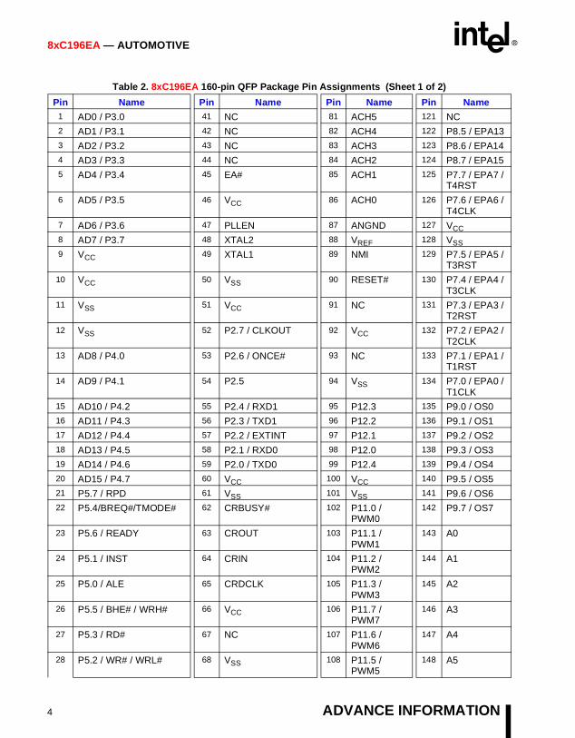
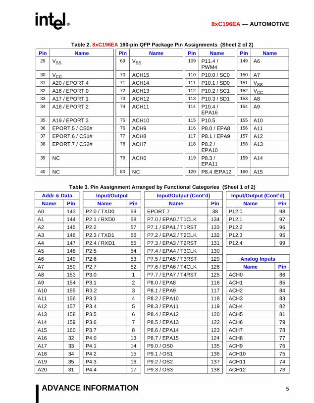
Table 2. 8xC196EA 160-pin QFP Package Pin Assignments (Sheet 1 of 2)
Pin Name Pin Name Pin Name Pin Name1 AD0 / P3.0 41 NC 81 ACH5 121 NC2 AD1 / P3.1 42 NC 82 ACH4 122 P8.5 / EPA133 AD2 / P3.2 43 NC 83 ACH3 123 P8.6 / EPA14 4 AD3 / P3.3 44 NC 84 ACH2 124 P8.7 / EPA15 5 AD4 / P3.4 45 EA# 85 ACH1 125 P7.7 / EPA7 /
T4RST
6 AD5 / P3.5 46 VCC 86 ACH0 126 P7.6 / EPA6 / T4CLK
7 AD6 / P3.6 47 PLLEN 87 ANGND 127 VCC
8 AD7 / P3.7 48 XTAL2 88 VREF 128 VSS
9 VCC 49 XTAL1 89 NMI 129 P7.5 / EPA5 / T3RST
10 VCC 50 VSS 90 RESET# 130 P7.4 / EPA4 / T3CLK
11 VSS 51 VCC 91 NC 131 P7.3 / EPA3 / T2RST
12 VSS 52 P2.7 / CLKOUT 92 VCC 132 P7.2 / EPA2 / T2CLK
13 AD8 / P4.0 53 P2.6 / ONCE# 93 NC 133 P7.1 / EPA1 / T1RST
14 AD9 / P4.1 54 P2.5 94 VSS 134 P7.0 / EPA0 / T1CLK
15 AD10 / P4.2 55 P2.4 / RXD1 95 P12.3 135 P9.0 / OS0 16 AD11 / P4.3 56 P2.3 / TXD1 96 P12.2 136 P9.1 / OS117 AD12 / P4.4 57 P2.2 / EXTINT 97 P12.1 137 P9.2 / OS218 AD13 / P4.5 58 P2.1 / RXD0 98 P12.0 138 P9.3 / OS319 AD14 / P4.6 59 P2.0 / TXD0 99 P12.4 139 P9.4 / OS420 AD15 / P4.7 60 VCC 100 VCC 140 P9.5 / OS521 P5.7 / RPD 61 VSS 101 VSS 141 P9.6 / OS622 P5.4/BREQ#/TMODE# 62 CRBUSY# 102 P11.0 /
PWM0 142 P9.7 / OS7
23 P5.6 / READY 63 CROUT 103 P11.1 / PWM1
143 A0
24 P5.1 / INST 64 CRIN 104 P11.2 / PWM2
144 A1
25 P5.0 / ALE 65 CRDCLK 105 P11.3 / PWM3
145 A2
26 P5.5 / BHE# / WRH# 66 VCC 106 P11.7 / PWM7
146 A3
27 P5.3 / RD# 67 NC 107 P11.6 / PWM6
147 A4
28 P5.2 / WR# / WRL# 68 VSS 108 P11.5 / PWM5
148 A5
4 ADVANCE INFORMATION
8xC196EA — AUTOMOTIVE
29 VSS 69 VSS 109 P11.4 / PWM4
149 A6
30 VCC 70 ACH15 110 P10.0 / SC0 150 A731 A20 / EPORT.4 71 ACH14 111 P10.1 / SD0 151 VSS
32 A16 / EPORT.0 72 ACH13 112 P10.2 / SC1 152 VCC
33 A17 / EPORT.1 73 ACH12 113 P10.3 / SD1 153 A834 A18 / EPORT.2 74 ACH11 114 P10.4 /
EPA16154 A9
35 A19 / EPORT.3 75 ACH10 115 P10.5 155 A1036 EPORT.5 / CS0# 76 ACH9 116 P8.0 / EPA8 156 A1137 EPORT.6 / CS1# 77 ACH8 117 P8.1 / EPA9 157 A1238 EPORT.7 / CS2# 78 ACH7 118 P8.2 /
EPA10 158 A13
39 NC 79 ACH6 119 P8.3 / EPA11
159 A14
40 NC 80 NC 120 P8.4 /EPA12 160 A15
Table 3. Pin Assignment Arranged by Functional Categories (Sheet 1 of 2)
Addr & Data Input/Output Input/Output (Cont’d) Input/Output (Cont’d)
Name Pin Name Pin Name Pin Name Pin
A0 143 P2.0 / TXD0 59 EPORT.7 38 P12.0 98
A1 144 P2.1 / RXD0 58 P7.0 / EPA0 / T1CLK 134 P12.1 97
A2 145 P2.2 57 P7.1 / EPA1 / T1RST 133 P12.2 96
A3 146 P2.3 / TXD1 56 P7.2 / EPA2 / T2CLK 132 P12.3 95
A4 147 P2.4 / RXD1 55 P7.3 / EPA3 / T2RST 131 P12.4 99
A5 148 P2.5 54 P7.4 / EPA4 / T3CLK 130
A6 149 P2.6 53 P7.5 / EPA5 / T3RST 129 Analog Inputs
A7 150 P2.7 52 P7.6 / EPA6 / T4CLK 126 Name Pin
A8 153 P3.0 1 P7.7 / EPA7 / T4RST 125 ACH0 86
A9 154 P3.1 2 P8.0 / EPA8 116 ACH1 85
A10 155 R3.2 3 P8.1 / EPA9 117 ACH2 84
A11 156 P3.3 4 P8.2 / EPA10 118 ACH3 83
A12 157 P3.4 5 P8.3 / EPA11 119 ACH4 82
A13 158 P3.5 6 P8.4 / EPA12 120 ACH5 81
A14 159 P3.6 7 P8.5 / EPA13 122 ACH6 79
A15 160 P3.7 8 P8.6 / EPA14 123 ACH7 78
A16 32 P4.0 13 P8.7 / EPA15 124 ACH8 77
A17 33 P4.1 14 P9.0 / OS0 135 ACH9 76
A18 34 P4.2 15 P9.1 / OS1 136 ACH10 75
A19 35 P4.3 16 P9.2 / OS2 137 ACH11 74
A20 31 P4.4 17 P9.3 / OS3 138 ACH12 73
Table 2. 8xC196EA 160-pin QFP Package Pin Assignments (Sheet 2 of 2)
Pin Name Pin Name Pin Name Pin Name
ADVANCE INFORMATION 5
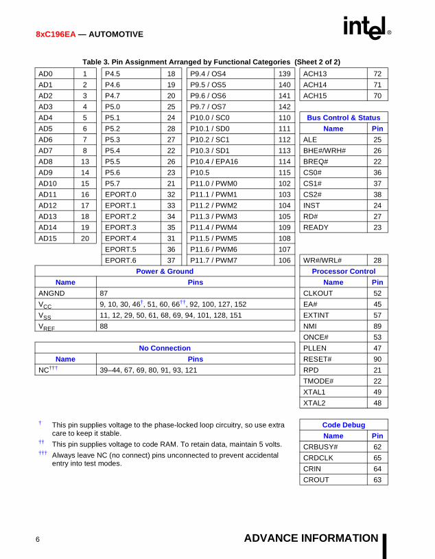
8xC196EA — AUTOMOTIVE
AD0 1 P4.5 18 P9.4 / OS4 139 ACH13 72
AD1 2 P4.6 19 P9.5 / OS5 140 ACH14 71
AD2 3 P4.7 20 P9.6 / OS6 141 ACH15 70
AD3 4 P5.0 25 P9.7 / OS7 142
AD4 5 P5.1 24 P10.0 / SC0 110 Bus Control & Status
AD5 6 P5.2 28 P10.1 / SD0 111 Name Pin
AD6 7 P5.3 27 P10.2 / SC1 112 ALE 25
AD7 8 P5.4 22 P10.3 / SD1 113 BHE#/WRH# 26
AD8 13 P5.5 26 P10.4 / EPA16 114 BREQ# 22
AD9 14 P5.6 23 P10.5 115 CS0# 36
AD10 15 P5.7 21 P11.0 / PWM0 102 CS1# 37
AD11 16 EPORT.0 32 P11.1 / PWM1 103 CS2# 38
AD12 17 EPORT.1 33 P11.2 / PWM2 104 INST 24
AD13 18 EPORT.2 34 P11.3 / PWM3 105 RD# 27
AD14 19 EPORT.3 35 P11.4 / PWM4 109 READY 23
AD15 20 EPORT.4 31 P11.5 / PWM5 108
EPORT.5 36 P11.6 / PWM6 107
EPORT.6 37 P11.7 / PWM7 106 WR#/WRL# 28
Power & Ground Processor Control
Name Pins Name Pin
ANGND 87 CLKOUT 52
VCC 9, 10, 30, 46†, 51, 60, 66††, 92, 100, 127, 152 EA# 45
VSS 11, 12, 29, 50, 61, 68, 69, 94, 101, 128, 151 EXTINT 57
VREF 88 NMI 89
ONCE# 53
No Connection PLLEN 47
Name Pins RESET# 90
NC††† 39–44, 67, 69, 80, 91, 93, 121 RPD 21
TMODE# 22
XTAL1 49
XTAL2 48
† This pin supplies voltage to the phase-locked loop circuitry, so use extra care to keep it stable.
†† This pin supplies voltage to code RAM. To retain data, maintain 5 volts.††† Always leave NC (no connect) pins unconnected to prevent accidental
entry into test modes.
Code Debug
Name Pin
CRBUSY# 62
CRDCLK 65
CRIN 64
CROUT 63
Table 3. Pin Assignment Arranged by Functional Categories (Sheet 2 of 2)
6 ADVANCE INFORMATION

8xC196EA — AUTOMOTIVE
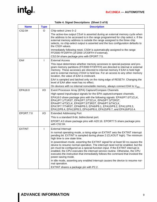
4.0 SIGNALS
Table 4. Signal Descriptions (Sheet 1 of 8)
Name Type Description
A15:0 O System Address BusThese address lines provide address bits 0–15 during the entire external mem-ory cycle during both multiplexed and demultiplexed bus modes.
A20:16 I/O Address Lines 16–20These address lines provide address bits 16–20 during the entire external memory cycle, supporting extended addressing of the 2 Mbyte address space.NOTE: Internally, there are 24 address bits; however, only 21 external
address pins (A20:0) are implemented. The internal address space is16 Mbytes (000000 FFFFFFH) and the external address space is2 Mbytes (00000 1FFFFFH). The device resets to FF2080H in internalmemory or 1F2080H in external memory.
A20:16 are multiplexed with EPORT.4:0.
ACH15:0 I Analog ChannelsThese pins are analog inputs to the A/D converter.
The ANGND and VREF pins must be connected for the A/D converter to function.
AD15:0 I/O Address/Data LinesThe function of these pins depend on the bus size and mode. When a bus access is not occurring, these pins revert to their I/O port function.16-bit Multiplexed Bus Mode:AD15:0 drive address bits 0–15 during the first half of the bus cycle and drive or receive data during the second half of the bus cycle.8-bit Multiplexed Bus Mode:AD15:8 drive address bits 8–15 during the entire bus cycle. AD7:0 drive address bits 0–7 during the first half of the bus cycle and drive or receive data during the second half of the bus cycle.16-bit Demultiplexed Mode:AD15:0 drive or receive data during the entire bus cycle.8-bit Demultiplexed Mode:AD7:0 drive or receive data during the entire bus cycle. AD15:8 drive the data that is currently on the high byte of the internal bus.AD7:0 share package pins P3.7:0. AD15:8 share package pins P4.7:0.
ALE O Address Latch EnableThis active-high output signal is asserted only during external memory cycles. ALE signals the start of an external bus cycle and indicates that valid address information is available on the system address/data bus (A20:16 and AD15:0 for a multiplexed bus; A20:0 for a demultiplexed bus). An external latch can use this signal to demultiplex address bits 0–15 from the address/data bus in multiplexed mode.ALE shares a package pin with P5.0.
ANGND GND Analog GroundANGND must be connected for A/D converter operation. ANGND and VSS should be nominally at the same potential.
ADVANCE INFORMATION 7

8xC196EA — AUTOMOTIVE
BHE# O Byte High Enable†
During 16-bit bus cycles, this active-low output signal is asserted for word and high-byte reads and writes to external memory. BHE# indicates that valid data is being transferred over the upper half of the system data bus. Use BHE#, in conjunction with AD0, to determine which memory byte is being transferred over the system bus:
BHE# AD0 Byte(s) Accessed
0 0 both bytes0 1 high byte only1 0 low byte only
BHE# shares a package pin with P5.5 and WRH#.† The chip configuration register 0 (CCR0) determines whether this pin func-
tions as BHE# or WRH#. CCR0.2 = 1 selects BHE#; CCR0.2 = 0 selects WRH#.
BREQ# O Bus RequestThis active-low output signal is asserted during a hold cycle when the bus con-troller has a pending external memory cycle.You must enable the bus-hold protocol before using this signal.BREQ# shares a package pin with P5.4.
CLKOUT O Clock OutputOutput of the internal clock generator. The CLKOUT frequency can be pro-grammed to one of five frequencies: the internal operating frequency (f) divided by a factor of two, four, eight, or sixteen, or the same frequency as the oscillator input (FXTAL1). CLKOUT has a 50% duty cycle.CLKOUT shares a package pin with P2.7
CRBUSY# O Code RAM BusyThis signal indicates that the serial debug unit (SDU) is not ready to conduct a transaction.
CRDCLK I Code RAM ClockProvides the clock signal for the serial debug unit (SDU). The maximum clock frequency equals the operating frequency (f) divided by two.
CRIN I Code RAM Data InputSerial input for test instructions and data into the serial debug unit (SDU). Data is transferred in 8-bit bytes with the most-significant bit (MSB) first. Each bit is sampled on the rising edge of CRDCLK.
CROUT O Code RAM Data OutputSerial output for data from the serial debug unit (SDU). Data is transferred in 8-bit bytes with the most-significant bit (MSB) first. Each bit is valid on the rising edge of CRDCLK.
Table 4. Signal Descriptions (Sheet 2 of 8)
Name Type Description
8 ADVANCE INFORMATION
8xC196EA — AUTOMOTIVE
CS2:0# O Chip-select Lines 0–2The active-low output CSx# is asserted during an external memory cycle when the address to be accessed is in the range programmed for chip select x. If the external memory address is outside the range assigned to the three chip selects, no chip-select output is asserted and the bus configuration defaults to the CS2# values.Immediately following reset, CS0# is automatically assigned to the range FF2000 FF20FFH (1F2000 1F20FFH if external).CS2:0# share package pins with EPORT.7:5.
EA# I External AccessThis input determines whether memory accesses to special-purpose and pro-gram memory partitions (FF2000 FF3FFFH) are directed to internal or external memory. These accesses are directed to internal memory if EA# is held high and to external memory if EA# is held low. For an access to any other memory location, the value of EA# is irrelevant.EA# is sampled and latched only on the rising edge of RESET#. Changing the level of EA# after reset has no effect. On devices with no internal nonvolatile memory, always connect EA# to VSS.
EPA16:0 I/O Event Processor Array (EPA) Capture/Compare ChannelsHigh-speed input/output signals for the EPA capture/compare channels. EPA16:0 share package pins with the following signals: EPA0/P7.0/T1CLK, EPA1/P7.1/T1RST, EPA2/P7.2/T2CLK, EPA3/P7.3/T2RST, EPA4/P7.4/T3CLK, EPA5/P7.5/T3RST, EPA6/P7.6/T4CLK, EPA7/P7.7/T4RST, EPA8/P8.0, EPA9/P8.1, EPA10/P8.2, EPA11/P8.3, EPA12/P8.4, EPA13/P8.5, EPA14/P8.6, EPA15/P8.7, and EPA16/P10.4.
EPORT.7:0 I/O Extended Addressing Port
This is a standard 8-bit, bidirectional port.
EPORT.4:0 share package pins with A20:16. EPORT7:5 share package pins with CS2:0#.
EXTINT I External InterruptIn normal operating mode, a rising edge on EXTINT sets the EXTINT interrupt pending bit. EXTINT is sampled during phase 2 (CLKOUT high). The minimum high time is one state time.In powerdown mode, asserting the EXTINT signal for at least 50 ns causes the device to resume normal operation. The interrupt need not be enabled, but the pin must be configured as a special-function input. If the EXTINT interrupt is enabled, the CPU executes the interrupt service routine. Otherwise, the CPU executes the instruction that immediately follows the command that invoked the power-saving mode.In idle mode, asserting any enabled interrupt causes the device to resume nor-mal operation.EXTINT shares a package pin with P2.2.
Table 4. Signal Descriptions (Sheet 3 of 8)
Name Type Description
ADVANCE INFORMATION 9
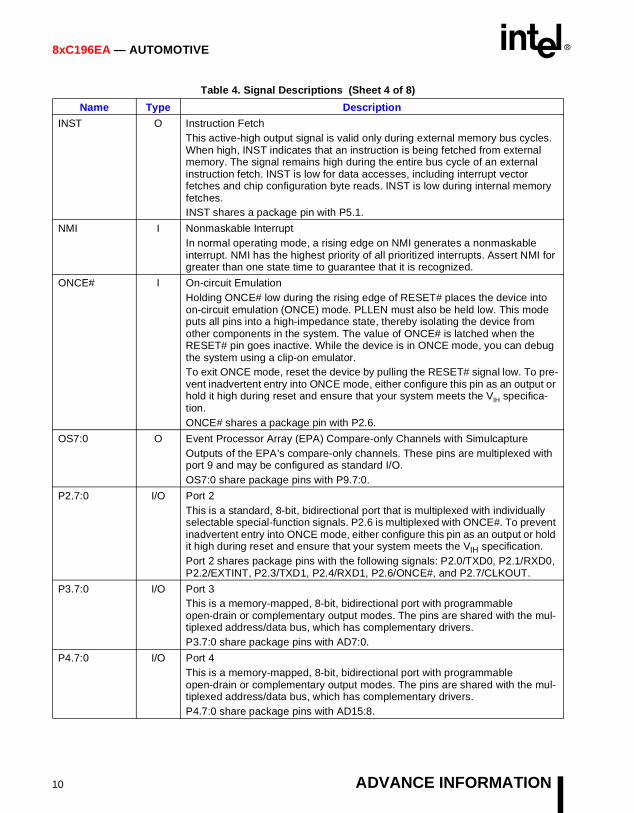
8xC196EA — AUTOMOTIVE
INST O Instruction FetchThis active-high output signal is valid only during external memory bus cycles. When high, INST indicates that an instruction is being fetched from external memory. The signal remains high during the entire bus cycle of an external instruction fetch. INST is low for data accesses, including interrupt vector fetches and chip configuration byte reads. INST is low during internal memory fetches.INST shares a package pin with P5.1.
NMI I Nonmaskable InterruptIn normal operating mode, a rising edge on NMI generates a nonmaskable interrupt. NMI has the highest priority of all prioritized interrupts. Assert NMI for greater than one state time to guarantee that it is recognized.
ONCE# I On-circuit EmulationHolding ONCE# low during the rising edge of RESET# places the device into on-circuit emulation (ONCE) mode. PLLEN must also be held low. This mode puts all pins into a high-impedance state, thereby isolating the device from other components in the system. The value of ONCE# is latched when the RESET# pin goes inactive. While the device is in ONCE mode, you can debug the system using a clip-on emulator. To exit ONCE mode, reset the device by pulling the RESET# signal low. To pre-vent inadvertent entry into ONCE mode, either configure this pin as an output or hold it high during reset and ensure that your system meets the VIH specifica-tion.ONCE# shares a package pin with P2.6.
OS7:0 O Event Processor Array (EPA) Compare-only Channels with SimulcaptureOutputs of the EPA’s compare-only channels. These pins are multiplexed with port 9 and may be configured as standard I/O.OS7:0 share package pins with P9.7:0.
P2.7:0 I/O Port 2This is a standard, 8-bit, bidirectional port that is multiplexed with individually selectable special-function signals. P2.6 is multiplexed with ONCE#. To prevent inadvertent entry into ONCE mode, either configure this pin as an output or hold it high during reset and ensure that your system meets the VIH specification.Port 2 shares package pins with the following signals: P2.0/TXD0, P2.1/RXD0, P2.2/EXTINT, P2.3/TXD1, P2.4/RXD1, P2.6/ONCE#, and P2.7/CLKOUT.
P3.7:0 I/O Port 3This is a memory-mapped, 8-bit, bidirectional port with programmable open-drain or complementary output modes. The pins are shared with the mul-tiplexed address/data bus, which has complementary drivers.P3.7:0 share package pins with AD7:0.
P4.7:0 I/O Port 4This is a memory-mapped, 8-bit, bidirectional port with programmable open-drain or complementary output modes. The pins are shared with the mul-tiplexed address/data bus, which has complementary drivers.P4.7:0 share package pins with AD15:8.
Table 4. Signal Descriptions (Sheet 4 of 8)
Name Type Description
10 ADVANCE INFORMATION

8xC196EA — AUTOMOTIVE
P5.7:0 I/O Port 5This is a memory-mapped, 8-bit, bidirectional port that is multiplexed with indi-vidually selectable control signals. P5.4 is multiplexed with TMODE#. If this pin is held low during reset, the device will enter a test mode. To prevent inadvert-ent entry into a reserved test mode, either configure this pin as an output or hold it high during reset and ensure that your system meets the VIH specifica-tion.Port 5 shares package pins with the following signals: P5.0/ALE, P5.1/INST, P5.2/WR#/WRL#, P5.3/RD#, P5.4/BREQ#/TMODE#, P5.5/BHE#/WRH#, P5.6/READY, and P5.7/RPD.
P7.7:0 I/O Port 7This is a standard, 8-bit, bidirectional port that is multiplexed with individually selectable special-function signals. Port 7 shares package pins with the following signals: P7.0/EPA0/T1CLK, P7.1/EPA1/T1RST, P7.2/EPA2/T2CLK, P7.3/EPA3/T2RST, P7.4/EPA4/T3CLK, P7.5/EPA5/T3RST, P7.6/EPA6/T4CLK, and P7.7/EPA7/T4RST.
P8.7:0 I/O Port 8This is a standard, 8-bit, bidirectional port that is multiplexed with individually selectable special-function signals. P8.7:0 share package pins with EPA15:8.
P9.7:0 I/O Port 9This is a standard, 8-bit, bidirectional port that is multiplexed with individually selectable special-function signals. P9.7:0 share package pins with OS7:0.
P10.5:0 I/O Port 10This is a standard, 6-bit, bidirectional port that is multiplexed with individually selectable special-function signals. Port 10 shares package pins with the following signals: P10.0/SC0, P10.1/SD0, P10.2/SC1, P10.3/SD1, P10.4/EPA16, and P10.5.
P11.7:0 I/O Port 11This is a standard, 8-bit, bidirectional port that is multiplexed with individually selectable special-function signals. P11.7:0 share package pins with PWM7:0.
P12.4:0 I/O Port 12This is a memory-mapped, 5-bit, bidirectional port. P12.2:0 select the test-ROM execution mode.
PLLEN I Phase-locked Loop EnableThis active-high input pin enables the on-chip clock doubler.This pin must be held low when entering on-circuit emulation (ONCE) mode.
PWM7:0 O Pulse Width Modulator OutputsThese are PWM output pins with high-current drive capability. PWM7:0 share package pins with P11.7:0.
Table 4. Signal Descriptions (Sheet 5 of 8)
Name Type Description
ADVANCE INFORMATION 11
8xC196EA — AUTOMOTIVE
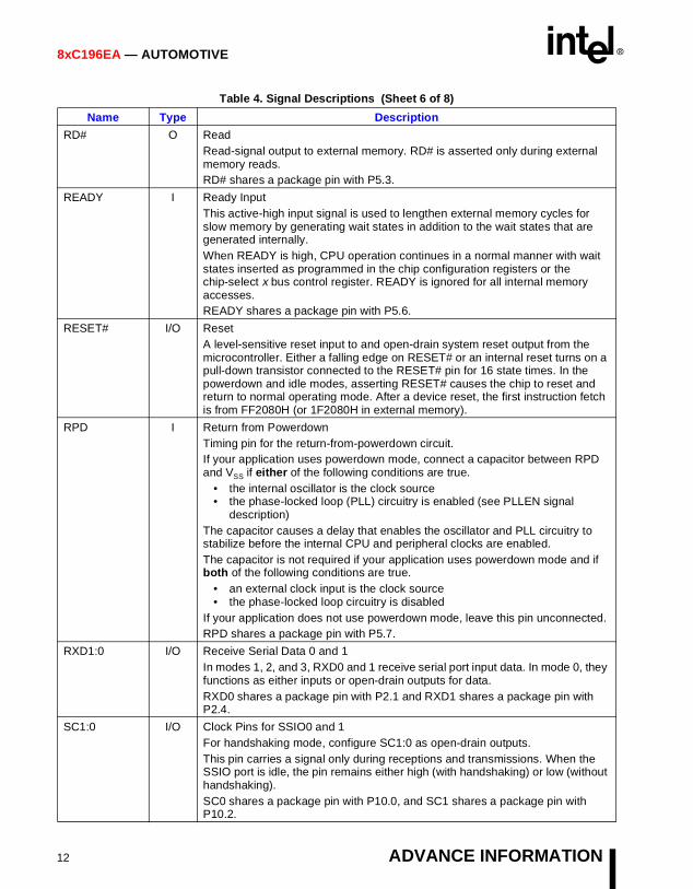
RD# O ReadRead-signal output to external memory. RD# is asserted only during external memory reads.RD# shares a package pin with P5.3.
READY I Ready InputThis active-high input signal is used to lengthen external memory cycles for slow memory by generating wait states in addition to the wait states that are generated internally. When READY is high, CPU operation continues in a normal manner with wait states inserted as programmed in the chip configuration registers or the chip-select x bus control register. READY is ignored for all internal memory accesses.READY shares a package pin with P5.6.
RESET# I/O ResetA level-sensitive reset input to and open-drain system reset output from the microcontroller. Either a falling edge on RESET# or an internal reset turns on a pull-down transistor connected to the RESET# pin for 16 state times. In the powerdown and idle modes, asserting RESET# causes the chip to reset and return to normal operating mode. After a device reset, the first instruction fetch is from FF2080H (or 1F2080H in external memory).
RPD I Return from PowerdownTiming pin for the return-from-powerdown circuit. If your application uses powerdown mode, connect a capacitor between RPD and VSS if either of the following conditions are true.
• the internal oscillator is the clock source • the phase-locked loop (PLL) circuitry is enabled (see PLLEN signal
description)The capacitor causes a delay that enables the oscillator and PLL circuitry to stabilize before the internal CPU and peripheral clocks are enabled. The capacitor is not required if your application uses powerdown mode and if both of the following conditions are true.
• an external clock input is the clock source • the phase-locked loop circuitry is disabled
If your application does not use powerdown mode, leave this pin unconnected.RPD shares a package pin with P5.7.
RXD1:0 I/O Receive Serial Data 0 and 1In modes 1, 2, and 3, RXD0 and 1 receive serial port input data. In mode 0, they functions as either inputs or open-drain outputs for data.RXD0 shares a package pin with P2.1 and RXD1 shares a package pin with P2.4.
SC1:0 I/O Clock Pins for SSIO0 and 1For handshaking mode, configure SC1:0 as open-drain outputs. This pin carries a signal only during receptions and transmissions. When the SSIO port is idle, the pin remains either high (with handshaking) or low (without handshaking).SC0 shares a package pin with P10.0, and SC1 shares a package pin with P10.2.
Table 4. Signal Descriptions (Sheet 6 of 8)
Name Type Description
12 ADVANCE INFORMATION

8xC196EA — AUTOMOTIVE
SD1:0 I/O Data Pins for SSIO0 and 1These pins are the data I/O pins for SSIO0 and 1.SD0 shares a package pin with P10.1, and SD1 shares a package pin with P10.1.
T1CLK I Timer 1 External ClockExternal clock for Timer 1.Timer 1 is programmable to increment or decement on the rising edge, the falling edge, or both rising and falling edges of T1CLK. T1CLK shares a package pin with P7.0 and EPA0.
T2CLK I Timer 2 External ClockExternal clock for timer 2. Timer 2 is programmable to increment or decement on the rising edge, the falling edge, or both rising and falling edges of T2CLK. External clock for the serial I/O baud-rate generator input (program selectable).T2CLK shares a package pin with P7.2 and EPA2.
T3CLK I Timer 3 External ClockExternal clock for timer 3. Timer 3 is programmable to increment or decement on the rising edge, the falling edge, or both rising and falling edges of T3CLK. T3CLK shares a package pin with P7.4 and EPA4.
T4CLK I Timer 4 External ClockExternal clock for timer 4. Timer 2 is programmable to increment or decement on the rising edge, the falling edge, or both rising and falling edges of T4CLK. T4CLK shares a package pin with P7.6 and EPA6.
T1RST I Timer 1 External ResetExternal reset for timer 1. Timer 1 is programmable to reset on the rising edge, the falling edge, or both rising and falling edges of T1RST. T1RST shares a package pin with P7.1 and EPA1.
T2RST I Timer 2 External ResetExternal reset for timer 2. Timer 2 is programmable to reset on the rising edge, the falling edge, or both rising and falling edges of T2RST. T2RST shares a package pin with P7.3 and EPA3.
T3RST I Timer 3 External ResetExternal reset for timer 3. Timer 3 is programmable to reset on the rising edge, the falling edge, or both rising and falling edges of T3RST. T3RST shares a package pin with P7.5 and EPA5.
T4RST I Timer 4 External ResetExternal reset for timer 4. Timer 4 is programmable to reset on the rising edge, the falling edge, or both rising and falling edges of T4RST. T4RST shares a package pin with P7.6 and EPA6.
TMODE# I Test-Mode EntryIf this pin is held low during reset, the device will enter a test mode. The value of several other pins defines the actual test mode. All test modes, except test-ROM execution, are reserved for Intel factory use. If you choose to config-ure this signal as an input, always hold it high during reset and ensure that your system meets the VIH specification to prevent inadvertent entry into test mode.TMODE# shares a package pin with P5.4 and BREQ#.
Table 4. Signal Descriptions (Sheet 7 of 8)
Name Type Description
ADVANCE INFORMATION 13

8xC196EA — AUTOMOTIVE
TXD1:0 O Transmit Serial Data 0 and 1In serial I/O modes 1, 2, and 3, TXD0 and 1 transmit serial port output data. In mode 0, they are the serial clock output.TXD0 shares a package pin with P2.0 and TXD1 shares a package pin with P2.3.
VCC PWR Digital Supply VoltageConnect each VCC pin to the digital supply voltage.
VREF PWR Reference Voltage for the A/D ConverterThis pin also supplies operating voltage to the analog portion of the A/D con-verter.
VSS GND Digital Circuit GroundThese pins supply ground for the digital circuitry. Connect each VSS pin to ground through the lowest possible impedance path.
WR# O Write†
This active-low output indicates that an external write is occurring. This signal is asserted only during external memory writes.WR# is multiplexed with P5.2 and WRL#.† The chip configuration register 0 (CCR0) determines whether this pin func-
tions as WR# or WRL#. CCR0.2 = 1 selects WR#; CCR0.2 = 0 selects WRL#.
WRH# O Write High†
During 16-bit bus cycles, this active-low output signal is asserted for high-byte writes and word writes to external memory. During 8-bit bus cycles, WRH# is asserted for all write operations.WRH# shares a package pin with P5.5 and BHE#.† The chip configuration register 0 (CCR0) determines whether this pin func-
tions as BHE# or WRH#. CCR0.2 = 1 selects BHE#; CCR0.2 = 0 selects WRH#.
WRL# O Write Low†
During 16-bit bus cycles, this active-low output signal is asserted for low-byte writes and word writes to external memory. During 8-bit bus cycles, WRL# is asserted for all write operations.WRL# shares a package pin with P5.2 and WR#.† The chip configuration register 0 (CCR0) determines whether this pin func-
tions as WR# or WRL#. CCR0.2 = 1 selects WR#; CCR0.2 = 0 selects WRL#.
XTAL1 I Input Crystal/Resonator or External Clock InputInput to the on-chip oscillator and the internal clock generators. The internal clock generators provide the peripheral clocks, CPU clock, and CLKOUT sig-nal. When using an external clock source instead of the on-chip oscillator, con-nect the clock input to XTAL1. The external clock signal must meet the VIH specification for XTAL1.
XTAL2 O Inverted Output for the Crystal/ResonatorOutput of the on-chip oscillator inverter. Leave XTAL2 floating when the design uses an external clock source instead of the on-chip oscillator.
Table 4. Signal Descriptions (Sheet 8 of 8)
Name Type Description
14 ADVANCE INFORMATION

8xC196EA — AUTOMOTIVE
5.0 ADDRESS MAP
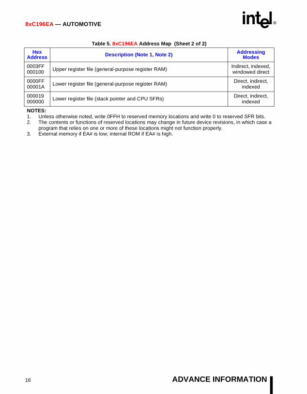
Table 5. 8xC196EA Address Map (Sheet 1 of 2)
HexAddress Description (Note 1, Note 2) Addressing
Modes
FFFFFFFF4000 External device (memory or I/O) connected to address/data bus Indirect, indexed,
extended
FF3FFFFF2400 Program memory (Note 3) Indirect, indexed,
extended
FF23FFFF2200 Program memory (Note 3) Indirect, indexed,
extended
FF21FFFF20C0 Special-purpose memory (PIH vectors; Note 3) Indirect, indexed,
extended
FF20BFFF2080
Program memory (Note 3); (After reset, the first instruction is fetched from FF2080H.)
Indirect, indexed, extended
FF207FFF2000 Special-purpose memory (CCBs, interrupt vectors, PTS vectors; Note 3) Indirect, indexed,
extended
FF1FFFFF1000 External device (memory or I/O) connected to address/data bus Indirect, indexed,
extended
FF0FFFFF0400 Internal code/data RAM (identically mapped from page 00H) Indirect, indexed,
extended
FF03FFFF0000 Reserved for in-circuit emulators —
FEFFFF1F0000
Overlaid memory (reserved for future devices);locations xF0000–xF03FFH are reserved for in-circuit emulators
Indirect, indexed, extended
1EFFFF004000 External device (memory or I/O) connected to address/data bus Indirect, indexed,
extended
003FFF002400
A copy of internal ROM (FF2400–FF3FFFH) if CCB1.2=0External memory if CCB1.2=1
Indirect, indexed, extended
0023FF002000 External device (memory or I/O) connected to address/data bus Indirect, indexed,
extended
001FFF001FE0 Memory-mapped special-function registers (SFRs) Indirect, indexed,
extended
001FDF001C00 Peripheral special-function registers (SFRs)
Indirect, indexed, extended,
windowed direct
001BFF001000 External device (memory or I/O) connected to address/data bus Indirect, indexed,
extended
000FFF000400 Internal code/data RAM (identically mapped into page FFH) Indirect, indexed,
extended
NOTES:1. Unless otherwise noted, write 0FFH to reserved memory locations and write 0 to reserved SFR bits.2. The contents or functions of reserved locations may change in future device revisions, in which case a
program that relies on one or more of these locations might not function properly. 3. External memory if EA# is low; internal ROM if EA# is high.
ADVANCE INFORMATION 15
8xC196EA — AUTOMOTIVE
0003FF000100 Upper register file (general-purpose register RAM) Indirect, indexed,
windowed direct
0000FF00001A Lower register file (general-purpose register RAM) Direct, indirect,
indexed
000019000000 Lower register file (stack pointer and CPU SFRs) Direct, indirect,
indexed
Table 5. 8xC196EA Address Map (Sheet 2 of 2)
HexAddress Description (Note 1, Note 2) Addressing
Modes
NOTES:1. Unless otherwise noted, write 0FFH to reserved memory locations and write 0 to reserved SFR bits.2. The contents or functions of reserved locations may change in future device revisions, in which case a
program that relies on one or more of these locations might not function properly. 3. External memory if EA# is low; internal ROM if EA# is high.
16 ADVANCE INFORMATION
8xC196EA — AUTOMOTIVE
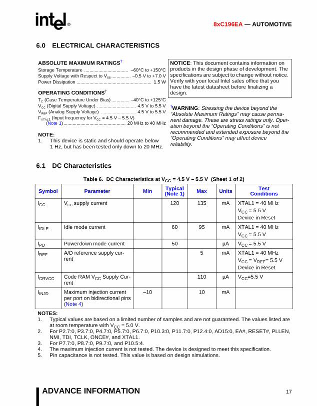
6.0 ELECTRICAL CHARACTERISTICS
6.1 DC Characteristics
ABSOLUTE MAXIMUM RATINGS†
Storage Temperature .................................. –60°C to +150°CSupply Voltage with Respect to VSS ............... –0.5 V to +7.0 VPower Dissipation .......................................................... 1.5 W
OPERATING CONDITIONS†
TC (Case Temperature Under Bias) .............. –40°C to +125°CVCC (Digital Supply Voltage) .............................. 4.5 V to 5.5 VVREF (Analog Supply Voltage) ........................... 4.5 V to 5.5 VFXTAL1 (Input frequency for VCC = 4.5 V – 5.5 V)
(Note 1) ................................................ 20 MHz to 40 MHz
NOTE:1. This device is static and should operate below
1 Hz, but has been tested only down to 20 MHz.
NOTICE: This document contains information on products in the design phase of development. The specifications are subject to change without notice. Verify with your local Intel sales office that you have the latest datasheet before finalizing a design.
†WARNING: Stressing the device beyond the “Absolute Maximum Ratings” may cause perma-nent damage. These are stress ratings only. Oper-ation beyond the “Operating Conditions” is not recommended and extended exposure beyond the “Operating Conditions” may affect device reliability.
Table 6. DC Characteristics at VCC = 4.5 V – 5.5 V (Sheet 1 of 2)
Symbol Parameter Min Typical (Note 1) Max Units Test
Conditions
ICC VCC supply current 120 135 mA XTAL1 = 40 MHzVCC = 5.5 VDevice in Reset
IIDLE Idle mode current 60 95 mA XTAL1 = 40 MHzVCC = 5.5 V
IPD Powerdown mode current 50 µA VCC = 5.5 V
IREF A/D reference supply cur-rent
5 mA XTAL1 = 40 MHzVCC = VREF= 5.5 VDevice in Reset
ICRVCC Code RAM VCC Supply Cur-rent
110 µA VCC=5.5 V
IINJD Maximum injection current per port on bidirectional pins (Note 4)
–10 10 mA
NOTES:1. Typical values are based on a limited number of samples and are not guaranteed. The values listed are
at room temperature with VCC = 5.0 V.2. For P2.7:0, P3.7:0, P4.7:0, P5.7:0, P6.7:0, P10.3:0, P11.7:0, P12.4:0, AD15:0, EA#, RESET#, PLLEN,
NMI, TDI, TCLK, ONCE#, and XTAL1.3. For P7.7:0, P8.7:0, P9.7:0, and P10.5:4.4. The maximum injection current is not tested. The device is designed to meet this specification.5. Pin capacitance is not tested. This value is based on design simulations.
ADVANCE INFORMATION 17
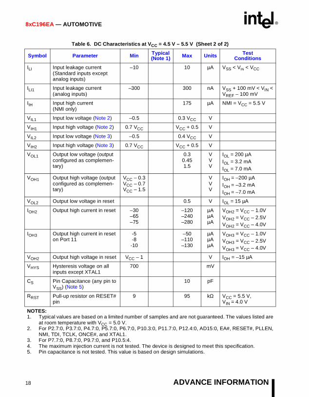
8xC196EA — AUTOMOTIVE
ILI Input leakage current (Standard inputs except analog inputs)
–10 10 µA VSS < VIN < VCC
ILI1 Input leakage current (analog inputs)
–300 300 nA VSS + 100 mV < VIN < VREF – 100 mV
IIH Input high current (NMI only)
175 µA NMI = VCC = 5.5 V
VIL1 Input low voltage (Note 2) –0.5 0.3 VCC V
VIH1 Input high voltage (Note 2) 0.7 VCC VCC + 0.5 V
VIL2 Input low voltage (Note 3) –0.5 0.4 VCC V
VIH2 Input high voltage (Note 3) 0.7 VCC VCC + 0.5 V
VOL1 Output low voltage (output configured as complemen-tary)
0.30.451.5
VVV
IOL = 200 µAIOL = 3.2 mAIOL = 7.0 mA
VOH1 Output high voltage (output configured as complemen-tary)
VCC – 0.3VCC – 0.7VCC – 1.5
VVV
IOH = –200 µAIOH = –3.2 mAIOH = –7.0 mA
VOL2 Output low voltage in reset 0.5 V IOL = 15 µA
IOH2 Output high current in reset –30–65–75
–120–240–280
µAµAµA
VOH2 = VCC – 1.0VVOH2 = VCC – 2.5VVOH2 = VCC – 4.0V
IOH3 Output high current in reset on Port 11
-5-8-10
–50–110–130
µAµAµA
VOH3 = VCC – 1.0VVOH3 = VCC – 2.5VVOH3 = VCC – 4.0V
VOH2 Output high voltage in reset VCC – 1 V IOH = –15 µA
VHYS Hysteresis voltage on all inputs except XTAL1
700 mV
CS Pin Capacitance (any pin to VSS) (Note 5)
10 pF
RRST Pull-up resistor on RESET# pin
9 95 kΩ VCC = 5.5 V, VIN = 4.0 V
Table 6. DC Characteristics at VCC = 4.5 V – 5.5 V (Sheet 2 of 2)
Symbol Parameter Min Typical (Note 1) Max Units Test
Conditions
NOTES:1. Typical values are based on a limited number of samples and are not guaranteed. The values listed are
at room temperature with VCC = 5.0 V.2. For P2.7:0, P3.7:0, P4.7:0, P5.7:0, P6.7:0, P10.3:0, P11.7:0, P12.4:0, AD15:0, EA#, RESET#, PLLEN,
NMI, TDI, TCLK, ONCE#, and XTAL1.3. For P7.7:0, P8.7:0, P9.7:0, and P10.5:4.4. The maximum injection current is not tested. The device is designed to meet this specification.5. Pin capacitance is not tested. This value is based on design simulations.
18 ADVANCE INFORMATION

8xC196EA — AUTOMOTIVE
6.2 AC Characteristics — Multiplexed Bus Mode
Test Conditions: Capacitive load on all pins = 50 pF, Rise and Fall Times = 3 ns.
Table 7. AC Characteristics, Multiplexed Bus Mode (Sheet 1 of 2)
Symbol Parameter Min Max Units
FXTAL1 Frequency on XTAL1, PLL in 1x mode 20 40 MHz (1, 8)
Frequency on XTAL1, PLL in 2x mode 10 20 MHz (8)
f Operating frequency, f = FXTAL1; PLL in 1x mode20 40 MHz (8)
Operating frequency, f = 2FXTAL1; PLL in 2x mode
t Period, t = 1/f 25 50 ns
TAVDV Address Valid to Input Data Valid 3t – 40 ns (2)
TRLDV RD# Low to Input Data Valid t – 18 ns (2)
TCHDV CLKOUT High to Input Data valid 2t – 35 ns (9)
TRHDZ RD# High to Input Data Float t + 5 ns
TRXDX Data Hold after RD# Inactive 0 ns
TXHCH XTAL1 Rising Edge to CLKOUT High or Low 3 50 ns (9)
TCLCL CLKOUT Cycle Time 2t ns (9)
TCHCL CLKOUT High Period t – 10 t + 10 ns (9)
TCLLH CLKOUT Falling to ALE Rising – 10 10 ns (9)
TLLCH ALE Falling to CLKOUT Rising – 10 10 ns (9)
TLHLH ALE Cycle Time 4t ns (2)
TLHLL ALE High Period t – 10 t + 10 ns
TAVLL Address Setup to ALE Low t – 15 ns
TLLAX Address Hold after ALE Low t – 15 ns
TLLRL ALE Low to RD# Low t – 15 ns
TRLCL RD# Low to CLKOUT Low – 10 10 ns (9)
TRLRH RD# Low to RD# High t – 12 ns (2)
TRHLH RD# High to ALE Rising t – 5 t + 15 ns (3)
NOTES:1. 20 MHz is the maximum input frequency when using an external crystal oscillator; however, 40 MHz
can be applied with an external clock source.2. If wait states are used, add 2t × n, where n = number of wait states.3. Assuming back-to-back bus cycles.4. When forcing wait states using the BUSCON register, add 2t × n.5. Exceeding the maximum specification causes additional wait states.6. 8-bit bus only.7. The first falling edge of READY is not synchronized to a CLKOUT edge; therefore, one programmed
wait state is required.8. Device is static by design but has been tested only down to 20 MHz.9. Assumes CLKOUT is operating in divide-by-two mode (f/2).
ADVANCE INFORMATION 19

8xC196EA — AUTOMOTIVE
TRLAZ RD# Low to Address Float 5 ns
TLLWL ALE Low to WR# Low t – 12 ns
TQVWH Data Stable to WR# Rising Edge t – 14 ns (2)
TCHWH CLKOUT High to WR# Rising Edge – 10 10 ns (9)
TWLWH WR# Low to WR# High t – 10 ns (2)
TWHQX Data Hold after WR# High t – 20 ns
TWHLH WR# High to ALE High t – 15 t + 10 ns
TWHBX BHE#, INST Hold after WR# High t – 4 ns
TWHAX AD15:8, CSx# Hold after WR# High t – 4 ns (6)
TRHBX BHE#, INST Hold after RD# High t – 5 ns
TRHAX AD15:8, CSx# Hold after RD# High t – 5 ns (6)
TWHSH A20:0, CSx# Hold after WR# High 0 ns
TRHSH A20:0, CSx# Hold after RD# High 0 ns
TAVYV AD15:0 Valid to READY Setup 2t – 40 ns (4)
TCLYX READY Hold after CLKOUT Low 0 2t – 40 ns (5, 7, 9)
TYLYH Non-READY Time No Upper Limit ns
Table 8. AC Timing Symbol Definitions
Signals Conditions
A† Address L ALE W WR#, WRH#, WRL# H High
B BHE# Q Output Data X XTAL1 L Low
C CLKOUT R RD# Y READY V Valid
D Input Data S CSx# X No Longer Valid
Z Floating† Address bus (demultiplexed mode) or address/data bus (multiplexed mode)
Table 7. AC Characteristics, Multiplexed Bus Mode (Sheet 2 of 2)
Symbol Parameter Min Max Units
NOTES:1. 20 MHz is the maximum input frequency when using an external crystal oscillator; however, 40 MHz
can be applied with an external clock source.2. If wait states are used, add 2t × n, where n = number of wait states.3. Assuming back-to-back bus cycles.4. When forcing wait states using the BUSCON register, add 2t × n.5. Exceeding the maximum specification causes additional wait states.6. 8-bit bus only.7. The first falling edge of READY is not synchronized to a CLKOUT edge; therefore, one programmed
wait state is required.8. Device is static by design but has been tested only down to 20 MHz.9. Assumes CLKOUT is operating in divide-by-two mode (f/2).
20 ADVANCE INFORMATION
8xC196EA — AUTOMOTIVE
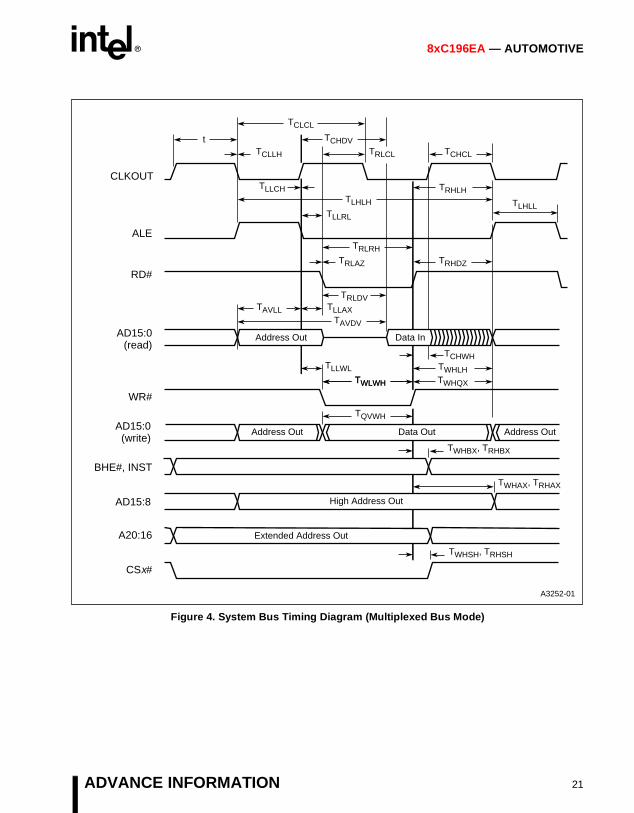
Figure 4. System Bus Timing Diagram (Multiplexed Bus Mode)
CLKOUT
ALE
RD#
A3252-01
AD15:0 (read)
WR#
AD15:0 (write)
BHE#, INST
AD15:8
A20:16
TLHLH
Address Out
Extended Address Out
tTCLLH
TCLCL
TCHDVTRLCL TCHCL
TLLCH
TLLRL
TRHLH
TRLRH
TRLDV
TRHDZ
Data In
TRLAZ
TLLAX
Address Out
TAVDV
TAVLL
TCHWHTWHLHTLLWL
TWLWH TWHQX
Data OutAddress Out
TWLWH
TQVWH
TWHBX, TRHBX
High Address Out
TWHSH, TRHSH
CSx#
TWHAX, TRHAX
TLHLL
ADVANCE INFORMATION 21

8xC196EA — AUTOMOTIVE
Figure 5. READY Timing Diagram (Multiplexed Bus Mode)
CLKOUT
READY
ALE
A3249-01
TCLYX (min)
TLHLH + 2t
TAVDV + 2t
RD#
AD15:0 (read)
AD15:0 (write)
BHE#, INST
A20:16
CSx#
TRLRH + 2t
TAVYV
Data Out
Extended Address Out
Address Out
TCLYX (max)
Data InAddress Out
TRLDV + 2t
TWLWH + 2t
TQVWH + 2t
WR#
22 ADVANCE INFORMATION

8xC196EA — AUTOMOTIVE
6.3 AC Characteristics — Demultiplexed Bus Mode
Test Conditions: Capacitive load on all pins = 50 pF, Rise and Fall Times = 3 ns.
Table 9. AC Characteristics, Demultiplexed Bus Mode (Sheet 1 of 2)
Symbol Parameter Min Max Units
FXTAL1 Frequency on XTAL1, PLL in 1x mode 20 40 MHz (1,8)
Frequency on XTAL1, PLL in 2x mode 10 20 MHz (8)
f Operating frequency, f = FXTAL1; PLL in 1x mode20 40 Mhz
Operating frequency, f = 2FXTAL1; PLL in 2x mode
t Period, t = 1/f 25 50 ns
TAVDV Address Valid to Input Data Valid 4t – 23 ns (2)
TRLDV RD# Low to Input Data Valid 3t – 25 ns (2)
TAVWL Address Valid to WR# Low t ns
TAVRL Address Valid to RD# Low t – 8 ns
TSLDV Chip Select Low to Data Valid 4t – 27 ns (2)
TCHDV CLKOUT Rising Edge to Input Data Valid 2t – 25 ns (9)
TRHDZ RD# High to Input Data Float t - 5 ns
TRHRL Read High to Next Read Low t – 5 ns
TRXDX Data Hold after RD# Inactive 0 ns
TXHCH XTAL1 High to CLKOUT High or Low 10 35 ns (9)
TCLCL CLKOUT Cycle Time 2t ns (9)
TCHCL CLKOUT High Period t – 10 t + 10 ns (9)
TCLLH CLKOUT Falling ALE Rising – 10 10 ns (9)
TRLCL RD# Low to CLKOUT Low – 5 5 ns (9)
TRLRH RD# Low to RD# High 3t – 12 ns (2)
TRHLH RD# Rising to ALE Rising t – 4 t + 12 ns (3)
TWLCL WR# Low to CLKOUT Falling – 12 5 ns (9)
TQVWH Data Stable to WR# Rising Edge 3t – 18 ns (3)
NOTES:1. 20 MHz is the maximum input frequency when using an external crystal oscillator; however, 40 MHz
can be applied with an external clock source.2. If wait states are used, add 2t × n, where n = number of wait states.3. Assuming back-to-back bus cycles.4. When forcing wait states using the BUSCON register, add 2t × n.5. Exceeding the maximum specification causes additional wait states.6. 8-bit bus only.7. The first falling edge of READY is not synchronized to a CLKOUT edge; therefore, one programmed
wait state is required.8. Device is static by design but has been tested only down to 20 MHz.9. Assumes CLKOUT is operating in divide-by-two mode (f/2).
ADVANCE INFORMATION 23
8xC196EA — AUTOMOTIVE
TCHWH CLKOUT High to WR# Rising Edge – 5 10 ns (9)
TWLWH WR# Low to WR# High 3t – 15 ns (2)
TWHQX Data Hold after WR# Rising Edge t t + 15 ns
TWHBX BHE#, INST Hold after WR# High t ns
TWHAX A20:0, CSx# Hold after WR# High 0 ns
TRHBX BHE#, INST Hold after RD# High t ns
TRHAX A20:0, CSx# Hold after RD# High 0 ns
TAVYV A20:0 Valid to READY Setup 3t – 25 ns (4)
TCLYX READY Hold after CLKOUT Low 0 2t – 28 ns(5, 7,9)
TYLYH Non READY Time No Upper Limit ns
Table 9. AC Characteristics, Demultiplexed Bus Mode (Sheet 2 of 2)
Symbol Parameter Min Max Units
NOTES:1. 20 MHz is the maximum input frequency when using an external crystal oscillator; however, 40 MHz
can be applied with an external clock source.2. If wait states are used, add 2t × n, where n = number of wait states.3. Assuming back-to-back bus cycles.4. When forcing wait states using the BUSCON register, add 2t × n.5. Exceeding the maximum specification causes additional wait states.6. 8-bit bus only.7. The first falling edge of READY is not synchronized to a CLKOUT edge; therefore, one programmed
wait state is required.8. Device is static by design but has been tested only down to 20 MHz.9. Assumes CLKOUT is operating in divide-by-two mode (f/2).
24 ADVANCE INFORMATION

8xC196EA — AUTOMOTIVE
Figure 6. System Bus Timing Diagram (Demultiplexed Bus Mode)
CLKOUT
ALE
RD#
A5397-01
AD15:0 (read)
WR#
AD15:0 (write)
BHE#, INST
A20:0 Address Out
TCHCL TCLCLTCHWH
TRHRLTRHDZ
Data In
TRLRH
TAVDV
TWHQXTWHAX
TWLCL
Data Out
TWLWH
TQVWH
TWHBX, TRHBX
CSx#
TCLLH
t
TRHLH
TAVRLTRHAX
TSLDV
TCHDVTRLDV
TAVWL
ADVANCE INFORMATION 25

8xC196EA — AUTOMOTIVE
Figure 7. READY Timing Diagram (Demultiplexed Bus Mode)
CLKOUT
READY
ALE
A5398-01
TCHYX (min)
TLHLH + 2t
TAVDV + 2t
RD#
AD15:0 (read)
AD15:0 (write)
BHE#, INST
A20:16
CSx#
TRLRH + 2t
TAVYV
Data Out
Extended Address Out
TCHYX (max)
Data In
TRLDV + 2t
TWLWH + 2t
TQVWH + 2t
WR#
26 ADVANCE INFORMATION

8xC196EA — AUTOMOTIVE
6.4 Deferred Bus Timing Mode
Deferred Bus Cycle Mode: This bus mode (enabledby setting CCB1.5) reduces bus contention whenusing the 8xC196EA in demultiplexed mode with
slow memories. As shown in Figure 8, a delay of 2toccurs in the first bus cycle following a chip-selectoutput change and the first write cycle following aread cycle.
Figure 8. Deferred Bus Mode Timing Diagram
CLKOUT
ALE
RD#
A3246-02
TWHLH + 2t
TRHLH + 2tTAVRL + 2t
TAVWL + 2tAD15:0
(read)
WR#
AD15:0 (write)
BHE#, INST
A20:0
CSx#
TAVDV+ 2t
TLHLH + 2t
Data InData In
Data Out
Valid Valid
Data Out
Address Out
Data Out
ADVANCE INFORMATION 27

8xC196EA — AUTOMOTIVE
6.5 AC Characteristics — Serial Port, Shift Register Mode
Figure 9. Serial Port Waveform — Shift Register Mode
Table 10. Serial Port Timing — Shift Register Mode
Symbol Parameter Min Max Units
TXLXL Serial Port Clock period
SP_BAUD ≥ x002HSP_BAUD = x001H†
6t4t
nsns
TXLXH Serial Port Clock falling edge to rising edge
SP_BAUD ≥ x002HSP_BAUD = x001H†
4t – 272t – 27
4t + 272t + 27
nsns
TQVXH Output data setup to clock high 4t – 30 ns
TXHQX Output data hold after clock high 2t – 30 ns
TXHQV Next output data valid after clock high 2t + 30 ns
TDVXH Input data setup to clock high 2t + 30 ns
TXHDX Input data hold after clock high 0 ns
TXHQZ Last clock high to output float t + 30 ns† The minimum baud-rate (SP_BAUD) register value for receive is x002H and the minimum baud-rate
(SP_BAUD) register value for transmit is x001H.
A2080-03
Valid Valid Valid Valid Valid Valid Valid ValidRXDx (In)
TXDx
0 1 2 3 4 5 6 7
TQVXH
TXLXL
TDVXH
TXHQVTXHQZ
TXHDX
TXHQXTXLXH
RXDx (Out)
28 ADVANCE INFORMATION

8xC196EA — AUTOMOTIVE
6.6 AC Characteristics — Synchronous Serial Port
Figure 10. Synchronous Serial Port
Table 11. Synchronous Serial Port Timing
Symbol Parameter Min Max Units
TCLCL Synchronous Serial Port Clock period 8t ns
TCLCH Synchronous Serial Port Clock falling edge to rising edge
4t ns
TD1DV Setup time for MSB output 2t ns
TCXDV Setup time for D6:0 output 3t + 20 ns
TCXDX Output data hold after clock low t 3t + 20 ns
TDVCX Setup time for input data 10 ns
TDXCX Input data hold after clock high t + 5 ns
A4512-01
D5 D4 D3 D2MSB D6 D1 D0
1 8765432
1 8765432
SCx (normal
transfers)
SDx (out)
SDx (in)
SCx(handshaking
transfers) Slave Receiver Pulls SCx low
TCLCL
TCLCH
STE Bit
TD1DV
TCXDX TCXDV
TDVCX TDXCX
valid valid valid valid valid valid valid valid
ADVANCE INFORMATION 29
8xC196EA — AUTOMOTIVE
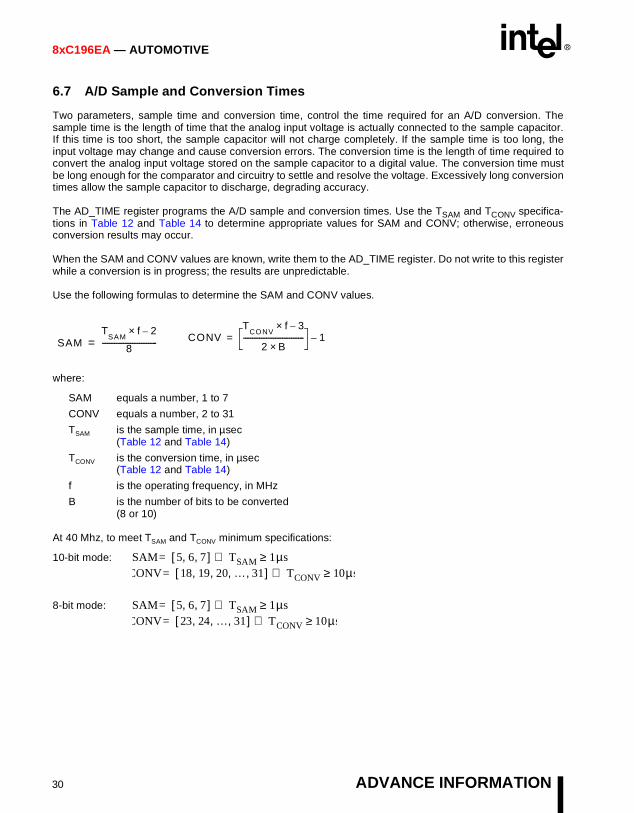
6.7 A/D Sample and Conversion Times
Two parameters, sample time and conversion time, control the time required for an A/D conversion. Thesample time is the length of time that the analog input voltage is actually connected to the sample capacitor.If this time is too short, the sample capacitor will not charge completely. If the sample time is too long, theinput voltage may change and cause conversion errors. The conversion time is the length of time required toconvert the analog input voltage stored on the sample capacitor to a digital value. The conversion time mustbe long enough for the comparator and circuitry to settle and resolve the voltage. Excessively long conversiontimes allow the sample capacitor to discharge, degrading accuracy.
The AD_TIME register programs the A/D sample and conversion times. Use the TSAM and TCONV specifica-tions in Table 12 and Table 14 to determine appropriate values for SAM and CONV; otherwise, erroneousconversion results may occur.
When the SAM and CONV values are known, write them to the AD_TIME register. Do not write to this registerwhile a conversion is in progress; the results are unpredictable.
Use the following formulas to determine the SAM and CONV values.
where:
SAM equals a number, 1 to 7
CONV equals a number, 2 to 31
TSAM is the sample time, in µsec (Table 12 and Table 14)
TCONV is the conversion time, in µsec (Table 12 and Table 14)
f is the operating frequency, in MHz
B is the number of bits to be converted(8 or 10)
At 40 Mhz, to meet TSAM and TCONV minimum specifications:
10-bit mode:
8-bit mode:
SAMT
SAMf 2–×
8-------------------------------= CONVT
CONVf× 3–
2 B×---------------------------------- 1–=
SAM 5 6 7, ,[ ]= TSAM 1µs≥⇒CONV 18 19 20 … 31, , , ,[ ]= TCONV 10µs≥⇒
SAM 5 6 7, ,[ ]= TSAM 1µs≥⇒CONV 23 24 … 31, , ,[ ]= TCONV 10µs≥⇒
30 ADVANCE INFORMATION

8xC196EA — AUTOMOTIVE
6.7.1 AC CHARACTERISTICS — A/D CONVERTER, 10-BIT MODE
Table 12. 10-bit A/D Operating Conditions ( 1)
Symbol Description Min Max Units Notes
TC Case Temperature – 40 + 125 °C
VCC Digital Supply Voltage 4.50 5.50 V
VREF Analog Supply Voltage 4.50 5.50 V 2
TSAM Sample Time 1.0 µs 3
TCONV Conversion Time 10.0 15.0 µs 3
NOTES:1. ANGND and VSS should nominally be at the same potential.2. VREF must not exceed VCC by more than + 0.5 V because VREF supplies both the resistor ladder and
the analog portion of the converter and input port pins.3. Program the AD_TIME register to meet the TSAM and TCONV specifications.
Table 13. 10-bit Mode A/D Characteristics Over Specified Operating Conditions (7) (Sheet 1 of 2)
Parameter Typical (2) Min Max Units (1) Notes
Resolution 102410
102410
Levels Bits
Absolute Error 0 ± 3.0 LSBs
Full-scale Error 0.25 ± 0.5 LSBs
Zero Offset Error 0.25 ± 0.5 LSBs
Nonlinearity 1.0 ± 2.0 ± 3.0 LSBs
Differential Nonlinearity – 0.75 + 0.75 LSBs
Channel-to-channel Matching ± 0.1 0 ± 1.0 LSBs
Repeatability ± 0.25 0 LSBs
Temperature Coefficients:OffsetFull-scaleDifferential Nonlinearity
0.0090.0090.009
LSB/CLSB/CLSB/C
Off-isolation – 60 dB 2, 3, 4
NOTES:1. An LSB, as used here, has a value of approximately 5 mV. 2. Most parts will meet these values at 25°C, but they are not tested or guaranteed.3. DC to 100 KHz.4. Multiplexer break-before-make guaranteed.5. Resistance from device pin, through internal multiplexer, to sample capacitor.6. Applying voltage beyond these specifications will degrade the accuracy of other channels being con-
verted.7. All conversions were performed with processor in idle mode.8. 100 mV < VIN < VREF – 100 mV.
ADVANCE INFORMATION 31
8xC196EA — AUTOMOTIVE
6.7.2 AC CHARACTERISTICS — A/D CONVERTER, 8-BIT MODE
Feedthrough – 60 dB 2, 3
VCC Power Supply Rejection – 60 dB 2, 3
Input Series Resistance 750 1.2K Ω 5
Voltage on Analog Input Pin ANGND VREF V 6
Sampling Capacitor 3.0 pF
DC Input Leakage ± 100 – 300 300 nA 8
Table 14. 8-bit A/D Operating Conditions (1)
Symbol Description Min Max Units Notes
TC Case Temperature – 40 + 125 °C
vCC Digital Supply Voltage 4.50 5.50 V
vREF Analog Supply Voltage 4.50 5.50 V 2
TSAM Sample Time 1.0 µs 3
TCONV Conversion Time 8.0 15.0 µs 3
NOTES:1. ANGND and VSS should nominally be at the same potential.2. VREF must not exceed VCC by more than + 0.5 V because VREF supplies both the resistor ladder and
the analog portion of the converter and input port pins.3. Program the AD_TIME register to meet the TSAM and TCONV specifications.
Table 13. 10-bit Mode A/D Characteristics Over Specified Operating Conditions (7) (Sheet 2 of 2)
Parameter Typical (2) Min Max Units (1) Notes
NOTES:1. An LSB, as used here, has a value of approximately 5 mV. 2. Most parts will meet these values at 25°C, but they are not tested or guaranteed.3. DC to 100 KHz.4. Multiplexer break-before-make guaranteed.5. Resistance from device pin, through internal multiplexer, to sample capacitor.6. Applying voltage beyond these specifications will degrade the accuracy of other channels being con-
verted.7. All conversions were performed with processor in idle mode.8. 100 mV < VIN < VREF – 100 mV.
32 ADVANCE INFORMATION

8xC196EA — AUTOMOTIVE
Table 15. 8-bit Mode A/D Characteristics Over Specified Operating Conditions (7)
Parameter Typical (2) Min Max Units (1) Notes
Resolution 2568
2568
Levels Bits
Absolute Error 0 ± 1.0 LSBs
Full-scale Error ± 0.5 LSBs
Zero Offset Error ± 0.5 LSBs
Nonlinearity 0 ± 1.0 LSBs
Differential Nonlinearity – 0.5 + 0.5 LSBs
Channel-to-channel Matching 0 ± 1.0 LSBs
Repeatability ± 0.25 0 LSBs
Temperature Coefficients:OffsetFull-scaleDifferential Nonlinearity
0.0030.0030.003
LSB/°CLSB/°CLSB/°C
Off Isolation – 60 dB 2, 3, 4
Feedthrough – 60 dB 2, 3
VCC Power Supply Rejection – 60 dB 2, 3
Input Series Resistance 750 1.2K Ω 5
Voltage on Analog Input Pin ANGND VREF V 6
Sampling Capacitor 3.0 pF
DC Input Leakage ±100 – 300 300 nA 8
NOTES:1. An LSB, as used here, has a value of approximately 20 mV. 2. Most parts will need these values at 25°C, but they are not tested or guaranteed.3. DC to 100 KHz.4. Multiplexer break-before-make guaranteed.5. Resistance from device pin, through internal multiplexer, to sample capacitor.6. Applying voltage beyond these specifications will degrade the accuracy of other channels being con-
verted.7. All conversions were performed with processor in idle mode.8. 100 mV < VIN < VREF – 100 mV.
ADVANCE INFORMATION 33
8xC196EA — AUTOMOTIVE
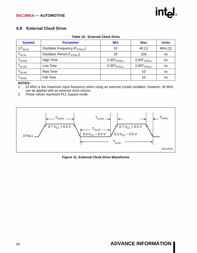
6.8 External Clock Drive
Figure 11. External Clock Drive Waveforms
Table 16. External Clock Drive
Symbol Parameter Min Max Units
1/TXLXL Oscillator Frequency (FXTAL1) 10 40 (1) MHz (2)
TXLXL Oscillator Period (TXTAL1) 25 100 ns
TXHXX High Time 0.35TXTAL1 0.65TXTAL1 ns
TXLXX Low Time 0.35TXTAL1 0.65TXTAL1 ns
TXLXH Rise Time 10 ns
TXHXL Fall Time 10 ns
NOTES:1. 20 MHz is the maximum input frequency when using an external crystal oscillator; however, 40 MHz
can be applied with an external clock source.2. These values represent PLL-bypass mode.
TXLXX
A2119-03
TXHXX TXHXL
TXLXL
0.3 VCC – 0.5 V
0.7 VCC + 0.5 V
TXLXH
0.7 VCC + 0.5 V
0.3 VCC – 0.5 VXTAL1
34 ADVANCE INFORMATION

8xC196EA — AUTOMOTIVE
6.9 Test Output Waveforms
Figure 12. AC Testing Output Waveforms
Figure 13. Float Waveforms During 5.0 Volt Testing
Test Points2.0 V
0.8 V
Note: AC testing inputs are driven at 3.5 V for a logic “1” and 0.45 V for a logic “0”. Timing measurements are made at 2.0 V for a logic “1” and 0.8 V for a logic “0”.
3.5 V
0.45 V
A2120-04
2.0 V
0.8 V
VLOAD
VLOAD – 0.15 V
VLOAD + 0.15 VTiming Reference
Points
VOH – 0.15 V
VOL + 0.15 V
Note: For timing purposes, a port pin is no longer floating when a 150 mV change from load voltage occurs and begins to float when a 150 mV change from the loading VOH/VOL level occurs with IOL/IOH ≤15 mA.
A2121-03
ADVANCE INFORMATION 35
8xC196EA — AUTOMOTIVE
7.0 THERMAL CHARACTERISTICS
All thermal impedance data is approximate for static air conditions at 1 W of power dissipation. Valueschange depending on operating conditions and the application. The Intel Packaging Handbook (order number240800) describes Intel’s thermal impedance test methodology. The Components Quality and ReliabilityHandbook (order number 210997) provides quality and reliability information.
7.1 8xC196EA Errata
The 8xC196EA may contain design defects or errors known as errata. Characterized errata that may causethe 8xC196EA’s behavior to deviate from published specifications are documented in a specification update.Specification updates can be obtained from your local Intel sales office or from the World Wide Web(www.intel.com).
Table 17. Thermal Characteristics
Package Type θJA θJC
160-pin QFP 34°C/W 5°C/W
36 ADVANCE INFORMATION
8xC196EA — AUTOMOTIVE
8.0 DATASHEET REVISION HISTORY
This datasheet is valid for devices with an “C” at the end of the topside field process order (FPO) number.Datasheets are changed as new device information becomes available. Verify with your local Intel salesoffice that you have the latest version before finalizing a design or ordering devices.
This is the -003 version of the datasheet. The following changes were made in this version:
Table 18. Revision History (rev. 002 - 003) (Sheet 1 of 2)
Item DescriptionData Sheet Added 80C196EA device to heading. All device references
changed to 8xC196EA.Figure 1 on page -1 Revised drawing to reflect “8xC196EA”.Table 4 on page -7 A15:0 - Type - Changed “I/O” to “O” only.
AD15:0 - Description - 8-bit Demultiplexed Mode: Added last para-graph “AD7:0 share package pins P3.7:0. AD15:8 share package pins P4.7:0.”CRIN - Description: Changed “byte” to “bit”.CROUT - Description: Changed “byte” to “bit”.ONCE# - Description - 1st paragraph: Added second sentence “PLLEN must also be held low.”PLLEN - Description: Added last paragraph “This pin must be held low when entering on-circuit emulation (ONCE) mode.”T1CLK - Description: Removed sentence “External clock for the serial I/O baud-rate generator input (program selectable).”T2CLK - Description: Added sentence “External clock for the serial I/O baud-rate generator input (program selectable).”XTAL1 - Description: Corrected spelling “sourcel” to “source”.
Table 6 on page -17 IPD:• Typical: Changed “20” to “50”• Max: Changed “50” to “blank”
IREF - Max: Changed TBD to “5”.ICRVCC - Added row.IHO2:
• Min: Changed VOH2=VCC-2.5 V to “-65”, VOH2=VCC-4.0 V to “-75”
• Units: Changed all from “mA” to “µA”IHO3:
• Parameter: Changed “Port 12”to “Port 11”• Min: Changed VOH3=VCC-1.0 V to “-5”, VOH3=VCC-2.5 V to
“-8”, VOH3=VCC-4.0 V to “-10”• Units: Changed all from “mA” to “µA”.
ADVANCE INFORMATION 37
8xC196EA — AUTOMOTIVE
Table 7 on page -19 FXTAL1 - Min:• 1x mode changed from “15” to “20”• 2x mode changed from “8” to “10”
f - Min: Changed from “15” to “20”.t - Max: Changed from “62.5” to “50”.TRLRH - Min: Changed from “t-10” to “t-12”.TCHWH - Max: Changed from “5” to “10”.TWHQX - Min: Changed from “t-15” to “t-20”.Note 1: “16 MHz” changed to “20 MHz”.
Table 9 on page -23 FXTAL1 - Min:• 1x mode changed from “15” to “20”• 2x mode changed from “8” to “10”
f - Min: Changed from “15” to “20”.t - Max: Changed from “62.5” to “50”.TCHCL - Min: Changed from “t-5” to “t-10”; Max: Changed from “t+5” to “t+10”.TCLLH - Min: Changed from “-5” to “-10”; Max: Changed from “5” to “10”.TRLRH - Min: Changed from “3t-10” to “3t-12”.TWLWH - Min: Changed from “3t-12” to “3t-15”.TAVYV - Max: Changed from “3t-23” to “3t-25”.Note 1: “16 MHz” changed to “20 MHz”.
Table 11 on page -29 TD1DV - Symbol: Changed TD1VD” to “TD1DV”.TD1DV - Min: Changed TBD to “2t”.
Figure 10 on page -29 Revised figure.Table 13 on page -31 DC Input Leakage
• Min - Changed “0” to “-300”• Max - Removed “±” from “300”
Note 2: Changed “need” to “meet”.Table 15 on page -33 DC Input Leakage:
• Typical: Added “±” to “100”• Min: Changed “0” to “-300”
Table 16 on page -34 1/TXLXL - Min: Changed “8” to “10”.TXLXL:
• Min: Changed “50” to “25”• Max: Changed “125” to “100”
Note 1:• Changed “16 MHz” to “20 MHz”• Changed “32 MHz” to “40 MHz”
Table 18. Revision History (rev. 002 - 003) (Sheet 2 of 2)
Item Description
38 ADVANCE INFORMATION

8xC196EA — AUTOMOTIVE
Table 19. Revision History (rev. 001 - 002)
Item Description
Data Sheet Status changed from “Product Preview” to “Advance Information”.
Cover The frequency designation was changed from 32 MHz to 40 MHz.
“DC Characteristics” on page -17 The following DC characteristics specifications were either changed or added:
• ICC (max)• IIDLE (max)
• IOH2 • IOH3
“AC Characteristics — Multiplexed Bus Mode” on page -19
The following AC characteristics multiplexed bus mode specifica-tions were changed:
• TCHCL (max)• TLLCH
(min/max)• TRLCL (max)• TCHWH (min)
• TWHLH (max)• TAVYV (max)• TCLYX (max)• TWHQX (min)
• TLLAX (min)• TRLDV (max)
“AC Characteristics — Demultiplexed Bus Mode” on page -23
The following AC characteristics demultiplexed bus mode speci-fications were changed:
• TAVDV (max)• TRLDV (max)• TSLDV (max)• TCHDV (max)• TXHCH
min/(max)• TCHCL
(min/max)• TCLLH
(min/max)
• TRLCL (min)• TRLRH (min)• TRHLH (max)• TWLCL (min)• TQVWH (min)• TCHWH (min)• TWLWH (min)
• TWHQX (max)• TWHBX (min)• TRHBX (min)• TAVYV (max)• TCLYX (max)
“AC Characteristics — Demultiplexed Bus Mode” on page -23
The following AC characteristics demultiplexed bus mode speci-fications were removed:
• TLLCH• TLHLH
• TLHLL • TWHLH
Figure 6 on page -25 Address out line in the System Bus Timing Diagram (Demulti-plexed Bus Mode) was corrected from A20:16 to A20:0.
Figure 5 on page -22 TCHYX (max) timing was corrected in the Ready Timing Diagram to show the rising edge of READY after the falling edge of CLKOUT.
HOLD#/HLDA# Timings Section was removed, and all references to either HOLD# or HLDA# were removed.
Table 11 on page -29 Synchronous Serial timing specifications changed in table.
“A/D Sample and Conversion Times” on page -30
A/D sample and conversion times example added.
Table 15 on page -33 Note 1 of the 8-bit mode A/D characteristics table changed to state 20 mV, instead of 5 mV.
ADVANCE INFORMATION 39

8xC196EA — AUTOMOTIVE
Table 20. Revision History (rev. 001)
Item Description
Table 17 Package thermal characteristics changed.
40 ADVANCE INFORMATION


![[XLS] · Web view6 16 5 6 16 5 6 16 5 6 16 5 6 16 5 6 16 5 6 16 5 6 16 5 6 16 5 6 16 5 6 16 5 6 16 5 6 16 5 6 16 5 6 16 5 616058570491 6 16 5 616056859737 6 16 5 616056143090 6 16](https://img.dokumen.tips/doc/110x75/5b2170327f8b9a86348b48ed/xls-web-view6-16-5-6-16-5-6-16-5-6-16-5-6-16-5-6-16-5-6-16-5-6-16-5-6-16-5.jpg)