Embed Size (px)
Citation preview

8-bit Microcontroller with 16K/32Kbytes In-SystemProgrammable Flash
ATmega16HVBATmega32HVB
8042E–AVR–09/2013
Features• High performance, low power Atmel® AVR® 8-bit Microcontroller• Advanced RISC architecture
– 131 powerful instructions - most single clock cycle execution– 32 × 8 general purpose working registers– Fully static operation– Up to eight MIPS throughput at 8MHz
• High endurance non-volatile memory segments– 16K/32Kbytes of in-system self-programmable flash (Atmel ATmega16HVB/32HVB)– 512/1Kbytes EEPROM– 1K/2Kbytes internal SRAM– Write/erase cycles 10,000 flash/100,000 EEPROM– Data retention: 20 years at 85°C/100 years at 25°C (1)
– Optional boot code section with independent lock bitsIn-system programming by on-chip boot programTrue read-while-write operation
– Programming lock for software security• Battery management features
– Two, three or four cells in series– High-current protection (charge and discharge)– Over-current protection (charge and discharge)– Short-circuit protection (discharge)– High-voltage outputs to drive N-channel charge/discharge FETs– Optional deep under voltage recovery mode - allowing 0-volt charging without
external precharge FET– Optional high-voltage open drain output - allowing 0-volt charging with external
precharge FET– Integrated cell balancing FETs
• Peripheral features– Two configurable 8-bit or 16-bit timers with separate prescaler, optional input
capture (IC), compare mode and CTC– SPI - serial peripheral interface– 12-bit voltage ADC, six external and one internal ADC input– High resolution coulomb counter ADC for current measurements– TWI serial interface supporting SMBus implementation– Programmable watchdog timer
• Special microcontroller features– debugWIRE on-chip debug system– In-system programmable via SPI ports– Power-on reset– On-chip voltage regulator with short-circuit monitoring interface– External and Internal interrupt sources– Sleep modes: idle, ADC noise reduction, power-save, and power-off
• Additional secure authentication features available only under NDA• Packages
– 44-pin TSSOP• Operating voltage: 4V -18V• Maximum withstand voltage (high-voltage pins): 35V• Temperature range: -40°C to 85°C• Speed grade: 1MHz - 8MHz
Note: 1. See ”Data retention” on page 8 for details.

1. Pin configurations
1.1 TSSOP
Figure 1-1. TSSOP - pinout the Atmel ATmega16HVB/32HVB.
1 44
3
PI
PPI
NV
PV1
PV2
PV3
PV4
PVT
VCC
GND
PC5
PC4(SCL)
PC3(INT3/SDA)
PC2(INT2)
PC1(INT1)
PC0(INT0/EXTPROT)
PB7(MISO/PCINT11)
NC
PB6(MOSI/PCINT10)
PB5(SCK/PCINT9)
PB4(SS/PCINT8)
PB3(PCINT7)
2
4
5
6
7
8
9
10
11
12
13
14
15
16
17
18
19
20
21
22
43
42
41
40
39
38
37
36
35
34
33
32
31
30
29
28
27
26
25
24
23
NI
NNI
VREFGND
VREF
GND
VREG
PA0(ADC0/SGND/PCINT0)
PA1(ADC1/SGND/PCINT1)
PA2(PCINT2/T0)
PA3(PCINT3/T1)
VCLMP10
VFET
BATT
VCC
GND
OD
NC
OC
RESET/dw
PB0(PCINT4/ICP00)
PB1(PCINT5/CKOUT)
PB2(PCINT6)
28042E–AVR–09/2013
ATmega16HVB/32HVB
ATmega16HVB/32HVB
1.2 Pin descriptions
1.2.1 VFET
High voltage supply pin. This pin is used as supply for the internal voltage regulator, described in”Voltage regulator” on page 129.
1.2.2 VCLMP10
Internal 10V clamping of VFET voltage for external decoupling.
1.2.3 VCC
Digital supply voltage. Normally connected to VREG.
1.2.4 VREG
Output from the internal voltage regulator. Used for external decoupling to ensure stable regula-tor operation. For details, see ”Voltage regulator” on page 129.
1.2.5 VREF
Internal voltage reference for external decoupling. For details, see ”Voltage reference and tem-perature sensor” on page 122.
1.2.6 VREFGND
Ground for decoupling of internal voltage reference. For details, see ”Voltage reference andtemperature sensor” on page 122. Do not connect to GND or SGND on PCB.
1.2.7 GND
Ground.
1.2.8 Port A (PA3..PA0)
Port A serves as a low-voltage 4-bit bi-directional I/O port with internal pull-up resistors (selectedfor each bit). As inputs, Port A pins that are externally pulled low will source current if the pull-upresistors are activated. The Port A pins are tri-stated when a reset condition becomes active,even if the clock is not running.
Port A also serves the functions of various special features of the Atmel ATmega16HVB/32HVBas listed in ”Alternate functions of Port A” on page 74.
1.2.9 Port B (PB7..PB0)
Port B is a low-voltage 8-bit bi-directional I/O port with internal pull-up resistors (selected foreach bit). As inputs, Port B pins that are externally pulled low will source current if the pull-upresistors are activated. The Port B pins are tri-stated when a reset condition becomes active,even if the clock is not running.
Port B also serves the functions of various special features of the ATmega16HVB/32HVB aslisted in ”Alternate functions of Port B” on page 75.
1.2.10 Port C (PC5)
Port C (PC5) is a high voltage Open Drain output port.
38042E–AVR–09/2013

1.2.11 Port C (PC4..PC0)
Port C is a 5-bit high voltage Open Drain bi-directional I/O port.
1.2.12 OC/OD
High voltage output to drive Charge/Discharge FET. For details, see ”FET driver” on page 145.
1.2.13 PI/NI
Filtered positive/negative input from external current sense resistor, used to by the CoulombCounter ADC to measure charge/discharge currents flowing in the battery pack. For details, see”Coulomb counter – Dedicated fuel gauging Sigma-Delta ADC” on page 108.
1.2.14 PPI/NNI
Unfiltered positive/negative input from external current sense resistor, used by the battery pro-tection circuit, for over-current and short-circuit detection. For details, see ”Battery protection” onpage 132.
1.2.15 NV/PV1/PV2/PV3/PV4
NV, PV1, PV2, PV3, and PV4 are the inputs for battery cells one, two, three and four, used bythe Voltage ADC to measure each cell voltage. For details, see ”Voltage ADC – 7-channel gen-eral purpose 12-bit Sigma-Delta ADC” on page 116.
1.2.16 PVT
Defines the source voltage level for the Charge FET driver. For details, see ”FET driver” on page145.
1.2.17 BATT
Input for detecting when a charger is connected. Defines the source voltage level for the Dis-charge FET driver. For details, see ”FET driver” on page 145.
1.2.18 RESET/dw
Reset input. A low level on this pin for longer than the minimum pulse length will generate areset, even if the clock is not running. The minimum pulse length is given in Table 32-3 on page227. Shorter pulses are not guaranteed to generate a reset. This pin is also used as debugWIREcommunication pin.
48042E–AVR–09/2013
ATmega16HVB/32HVB
ATmega16HVB/32HVB
2. Overview
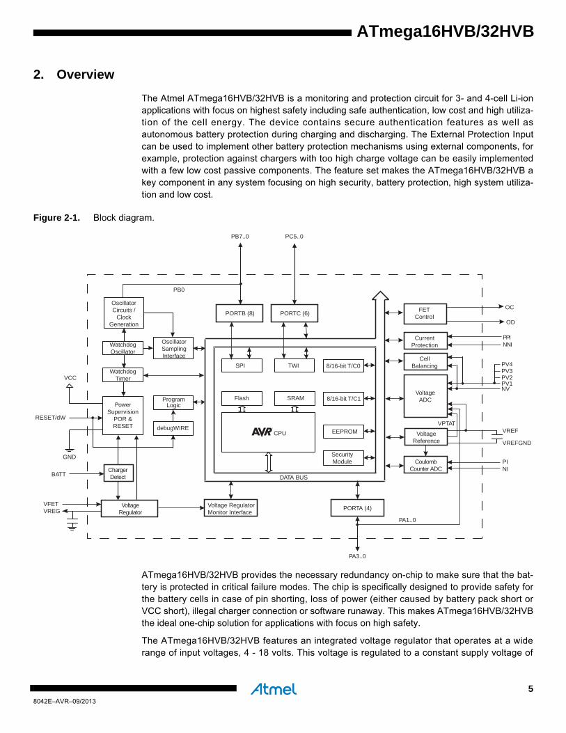
The Atmel ATmega16HVB/32HVB is a monitoring and protection circuit for 3- and 4-cell Li-ionapplications with focus on highest safety including safe authentication, low cost and high utiliza-tion of the cell energy. The device contains secure authentication features as well asautonomous battery protection during charging and discharging. The External Protection Inputcan be used to implement other battery protection mechanisms using external components, forexample, protection against chargers with too high charge voltage can be easily implementedwith a few low cost passive components. The feature set makes the ATmega16HVB/32HVB akey component in any system focusing on high security, battery protection, high system utiliza-tion and low cost.
Figure 2-1. Block diagram.
ATmega16HVB/32HVB provides the necessary redundancy on-chip to make sure that the bat-tery is protected in critical failure modes. The chip is specifically designed to provide safety forthe battery cells in case of pin shorting, loss of power (either caused by battery pack short orVCC short), illegal charger connection or software runaway. This makes ATmega16HVB/32HVBthe ideal one-chip solution for applications with focus on high safety.
The ATmega16HVB/32HVB features an integrated voltage regulator that operates at a widerange of input voltages, 4 - 18 volts. This voltage is regulated to a constant supply voltage of
PORTA (4)
SRAMFlash
CPU EEPROM
PV2
NV
OCFETControl
VoltageADC
VoltageReference
CoulombCounter ADC
GND
VCC
RESET/dW
PowerSupervision
POR &RESET
WatchdogOscillator
WatchdogTimer
OscillatorCircuits /
ClockGeneration
VREF
VREFGND
PINI
PA3..0
PA1..0
8/16-bit T/C1
8/16-bit T/C0
PORTB (8)
PB7..0
SPI
VoltageRegulator
ChargerDetect
VFETVREG
BATT
PV1
DATA BUS
VPTAT
CurrentProtection
SecurityModule
PORTC (6)
PC5..0
Voltage RegulatorMonitor Interface
PB0
OscillatorSamplingInterface
ProgramLogic
debugWIRE
CellBalancing
PV3PV4TWI
PPINNI
OD
58042E–AVR–09/2013

nominally 3.3 volts for the integrated logic and analog functions. The regulator capabilities, com-bined with an extremely low power consumption in the power saving modes, greatly enhancesthe cell energy utilization compared to existing solutions.
The chip utilizes the Atmel patented Deep Under-voltage Recovery (DUVR) mode that supportspre-charging of deeply discharged battery cells without using a separate Pre-charge FET. DUVRmode cannot be used in 2-cell applications. Optionally, Pre-charge FETs are supported for inte-gration into many existing battery charging schemes.
The battery protection monitors the charge and discharge current to detect illegal conditions andprotect the battery from these when required. A 12-bit Voltage ADC allows software to monitoreach cell voltage individually with high accuracy. The ADC also provides one internal input chan-nel to measure on-chip temperature and two input channels intended for external thermistors.An 18-bit ADC optimized for Coulomb Counting accumulates charge and discharge currents andreports accumulated current with high resolution and accuracy. It can also be used to provideinstantaneous current measurements with 13-bit resolution. Integrated Cell Balancing FETsallow cell balancing algorithms to be implemented in software.
The MCU provides the following features: 16K/32Kbytes of In-System Programmable Flash withRead-While-Write capabilities, 512/1Kbytes EEPROM, 1K/2Kbytes SRAM. 32 general purposeworking registers, 12 general purpose I/O lines, five general purpose high voltage open drain I/Olines, one general purpose super high voltage open drain output, debugWIRE for on-chip debug-ging and SPI for In-system Programming, a SM-Bus compliant TWI module, two flexibleTimer/Counters with Input Capture and compare modes.
Internal and external interrupts, a 12-bit Sigma Delta ADC for voltage and temperature measure-ments, a high resolution Sigma Delta ADC for Coulomb Counting and instantaneous currentmeasurements, integrated cell balancing FETs, Additional Secure Authentication Features, anautonomous Battery Protection module, a programmable Watchdog Timer with internal Oscilla-tor, and software selectable power saving modes.
The AVR core combines a rich instruction set with 32 general purpose working registers. All the32 registers are directly connected to the Arithmetic Logic Unit (ALU), allowing two independentregisters to be accessed in one single instruction executed in one clock cycle. The resultingarchitecture is more code efficient while achieving throughputs up to ten times faster than con-ventional CISC microcontrollers.
The device is manufactured using the Atmel high voltage high density non-volatile memory tech-nology. The On-chip ISP Flash allows the program memory to be reprogrammed In-System,through an SPI serial interface, by a conventional non-volatile memory programmer or by an On-chip Boot program running on the AVR core. The Boot program can use any interface to down-load the application program in the Application Flash memory. Software in the Boot Flashsection will continue to run while the Application Flash section is updated, providing true Read-While-Write operation. By combining an 8-bit RISC CPU with In-System Self-Programmable-Flash and highly accurate analog front-end in a monolithic chip.
The Atmel ATmega16HVB/32HVB is a powerful microcontroller that provides a highly flexibleand cost effective solution. It is part of the AVR Battery Management family that provides secureauthentication, highly accurate monitoring and autonomous protection for Lithium-ion batterycells.
The ATmega16HVB/32HVB AVR is supported with a full suite of program and system develop-ment tools including: C Compilers, Macro Assemblers, Program Debugger/Simulators, and On-chip Debugger.
68042E–AVR–09/2013
ATmega16HVB/32HVB
ATmega16HVB/32HVB
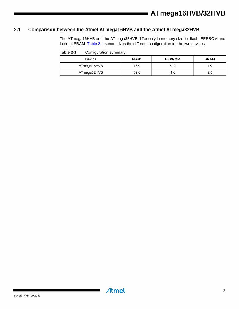
2.1 Comparison between the Atmel ATmega16HVB and the Atmel ATmega32HVB
The ATmega16HVB and the ATmega32HVB differ only in memory size for flash, EEPROM andinternal SRAM. Table 2-1 summarizes the different configuration for the two devices.
Table 2-1. Configuration summary.
Device Flash EEPROM SRAM
ATmega16HVB 16K 512 1K
ATmega32HVB 32K 1K 2K
78042E–AVR–09/2013

3. Disclaimer
All parameters contained in this datasheet are preliminary and based on characterization of theAtmel ATmega16/32HVB.
4. Resources
A comprehensive set of development tools, application notes and datasheets are available fordownload on http://www.atmel.com/avr.
Note: 1.
5. About code examples
This documentation contains simple code examples that briefly show how to use various parts ofthe device. These code examples assume that the part specific header file is included beforecompilation. Be aware that not all C compiler vendors include bit definitions in the header filesand interrupt handling in C is compiler dependent. Please confirm with the C compiler documen-tation for more details.
For I/O registers located in extended I/O map, “IN”, “OUT”, “SBIS”, “SBIC”, “CBI”, and “SBI”instructions must be replaced with instructions that allow access to extended I/O. Typically“LDS” and “STS” combined with “SBRS”, “SBRC”, “SBR”, and “CBR”.
6. Data retention
Reliability Qualification results show that the projected data retention failure rate is much lessthan one PPM over 20 years at 85°C or 100 years at 25°C.
88042E–AVR–09/2013
ATmega16HVB/32HVB

ATmega16HVB/32HVB
7. AVR CPU core
7.1 Overview
This section discusses the Atmel AVR core architecture in general. The main function of theCPU core is to ensure correct program execution. The CPU must therefore be able to accessmemories, perform calculations, control peripherals, and handle interrupts.
Figure 7-1. Block diagram of the AVR architecture.
In order to maximize performance and parallelism, the AVR uses a Harvard architecture – withseparate memories and buses for program and data. Instructions in the program memory areexecuted with a single level pipelining. While one instruction is being executed, the next instruc-tion is pre-fetched from the program memory. This concept enables instructions to be executedin every clock cycle. The program memory is In-System Reprogrammable Flash memory.
The fast-access Register File contains 32 × 8-bit general purpose working registers with a singleclock cycle access time. This allows single-cycle Arithmetic Logic Unit (ALU) operation. In a typ-
FlashProgramMemory
InstructionRegister
InstructionDecoder
ProgramCounter
Control Lines
32 x 8GeneralPurpose
Registrers
ALU
Statusand Control
I/O Lines
EEPROM
Data Bus 8-bit
DataSRAM
Dire
ct A
ddre
ssin
g
Indi
rect
Add
ress
ing
InterruptUnit
WatchdogTimer
I/O Module 2
I/O Module1
I/O Module n
98042E–AVR–09/2013

ical ALU operation, two operands are output from the Register File, the operation is executed,and the result is stored back in the Register File – in one clock cycle.
Six of the 32 registers can be used as three 16-bit indirect address register pointers for DataSpace addressing – enabling efficient address calculations. One of the these address pointerscan also be used as an address pointer for look up tables in Flash program memory. Theseadded function registers are the 16-bit X-register, Y-register, and Z-register, described later inthis section.
The ALU supports arithmetic and logic operations between registers or between a constant anda register. Single register operations can also be executed in the ALU. After an arithmetic opera-tion, the Status Register is updated to reflect information about the result of the operation.
Program flow is provided by conditional and unconditional jump and call instructions, able todirectly address the whole address space. Most AVR instructions have a single 16-bit word for-mat. Every program memory address contains a 16-bit or 32-bit instruction.
During interrupts and subroutine calls, the return address Program Counter (PC) is stored on theStack. The Stack is effectively allocated in the general data SRAM, and consequently the Stacksize is only limited by the total SRAM size and the usage of the SRAM. All user programs mustinitialize the SP in the Reset routine (before subroutines or interrupts are executed). The StackPointer (SP) is read/write accessible in the I/O space. The data SRAM can easily be accessedthrough the five different addressing modes supported in the AVR architecture.
The memory spaces in the AVR architecture are all linear and regular memory maps.
A flexible interrupt module has its control registers in the I/O space with an additional GlobalInterrupt Enable bit in the Status Register. All interrupts have a separate Interrupt Vector in theInterrupt Vector table. The interrupts have priority in accordance with their Interrupt Vector posi-tion. The lower the Interrupt Vector address, the higher the priority.
The I/O memory space contains 64 addresses for CPU peripheral functions as Control Regis-ters, SPI, and other I/O functions. The I/O Memory can be accessed directly, or as the DataSpace locations following those of the Register File, 0x20 - 0x5F. In addition, the AtmelATmega16HVB/32HVB has Extended I/O space from 0x60 - 0xFF in SRAM where only theST/STS/STD and LD/LDS/LDD instructions can be used.
7.2 ALU – Arithmetic Logic Unit
The high-performance AVR ALU operates in direct connection with all the 32 general purposeworking registers. Within a single clock cycle, arithmetic operations between general purposeregisters or between a register and an immediate are executed. The ALU operations are dividedinto three main categories – arithmetic, logical, and bit-functions. Some implementations of thearchitecture also provide a powerful multiplier supporting both signed/unsigned multiplicationand fractional format. See ”Instruction set summary” on page 259 for a detailed description.
7.3 Status Register
The Status Register contains information about the result of the most recently executed arithme-tic instruction. This information can be used for altering program flow in order to performconditional operations. Note that the Status Register is updated after all ALU operations, asspecified in the Instruction Set Reference. This will in many cases remove the need for using thededicated compare instructions, resulting in faster and more compact code.
108042E–AVR–09/2013
ATmega16HVB/32HVB
ATmega16HVB/32HVB
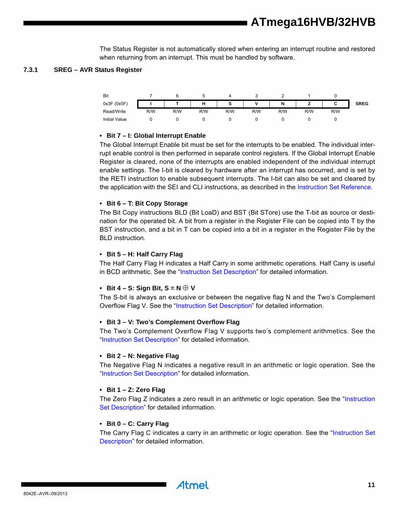
The Status Register is not automatically stored when entering an interrupt routine and restoredwhen returning from an interrupt. This must be handled by software.
7.3.1 SREG – AVR Status Register
• Bit 7 – I: Global Interrupt Enable
The Global Interrupt Enable bit must be set for the interrupts to be enabled. The individual inter-rupt enable control is then performed in separate control registers. If the Global Interrupt EnableRegister is cleared, none of the interrupts are enabled independent of the individual interruptenable settings. The I-bit is cleared by hardware after an interrupt has occurred, and is set bythe RETI instruction to enable subsequent interrupts. The I-bit can also be set and cleared bythe application with the SEI and CLI instructions, as described in the Instruction Set Reference.
• Bit 6 – T: Bit Copy Storage
The Bit Copy instructions BLD (Bit LoaD) and BST (Bit STore) use the T-bit as source or desti-nation for the operated bit. A bit from a register in the Register File can be copied into T by theBST instruction, and a bit in T can be copied into a bit in a register in the Register File by theBLD instruction.
• Bit 5 – H: Half Carry Flag
The Half Carry Flag H indicates a Half Carry in some arithmetic operations. Half Carry is usefulin BCD arithmetic. See the “Instruction Set Description” for detailed information.
• Bit 4 – S: Sign Bit, S = N V
The S-bit is always an exclusive or between the negative flag N and the Two’s ComplementOverflow Flag V. See the “Instruction Set Description” for detailed information.
• Bit 3 – V: Two’s Complement Overflow Flag
The Two’s Complement Overflow Flag V supports two’s complement arithmetics. See the“Instruction Set Description” for detailed information.
• Bit 2 – N: Negative Flag
The Negative Flag N indicates a negative result in an arithmetic or logic operation. See the“Instruction Set Description” for detailed information.
• Bit 1 – Z: Zero Flag
The Zero Flag Z indicates a zero result in an arithmetic or logic operation. See the “InstructionSet Description” for detailed information.
• Bit 0 – C: Carry Flag
The Carry Flag C indicates a carry in an arithmetic or logic operation. See the “Instruction SetDescription” for detailed information.
Bit 7 6 5 4 3 2 1 0
0x3F (0x5F) I T H S V N Z C SREG
Read/Write R/W R/W R/W R/W R/W R/W R/W R/W
Initial Value 0 0 0 0 0 0 0 0
118042E–AVR–09/2013
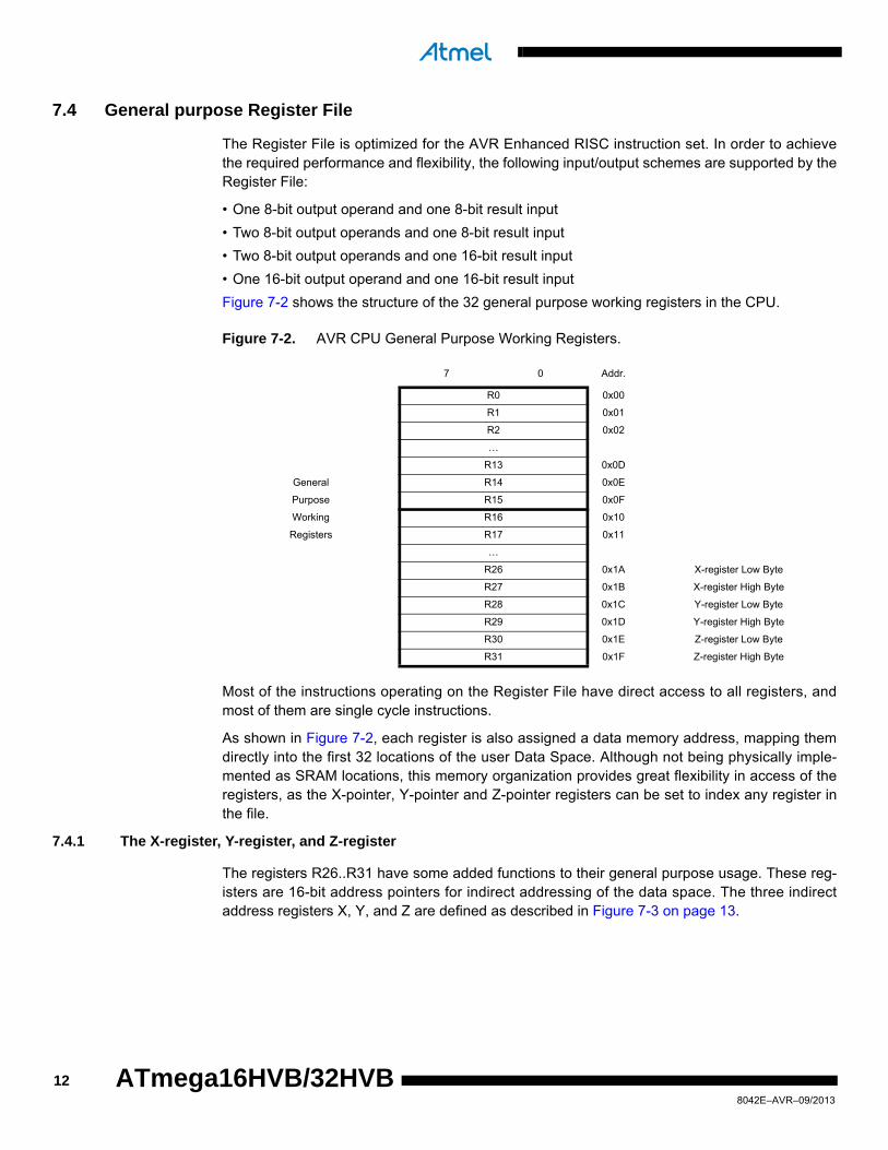
7.4 General purpose Register File
The Register File is optimized for the AVR Enhanced RISC instruction set. In order to achievethe required performance and flexibility, the following input/output schemes are supported by theRegister File:
• One 8-bit output operand and one 8-bit result input
• Two 8-bit output operands and one 8-bit result input
• Two 8-bit output operands and one 16-bit result input
• One 16-bit output operand and one 16-bit result input
Figure 7-2 shows the structure of the 32 general purpose working registers in the CPU.
Figure 7-2. AVR CPU General Purpose Working Registers.
Most of the instructions operating on the Register File have direct access to all registers, andmost of them are single cycle instructions.
As shown in Figure 7-2, each register is also assigned a data memory address, mapping themdirectly into the first 32 locations of the user Data Space. Although not being physically imple-mented as SRAM locations, this memory organization provides great flexibility in access of theregisters, as the X-pointer, Y-pointer and Z-pointer registers can be set to index any register inthe file.
7.4.1 The X-register, Y-register, and Z-register
The registers R26..R31 have some added functions to their general purpose usage. These reg-isters are 16-bit address pointers for indirect addressing of the data space. The three indirectaddress registers X, Y, and Z are defined as described in Figure 7-3 on page 13.
7 0 Addr.
R0 0x00
R1 0x01
R2 0x02
…
R13 0x0D
General R14 0x0E
Purpose R15 0x0F
Working R16 0x10
Registers R17 0x11
…
R26 0x1A X-register Low Byte
R27 0x1B X-register High Byte
R28 0x1C Y-register Low Byte
R29 0x1D Y-register High Byte
R30 0x1E Z-register Low Byte
R31 0x1F Z-register High Byte
128042E–AVR–09/2013
ATmega16HVB/32HVB

ATmega16HVB/32HVB
Figure 7-3. The X-register, Y-register, and Z-registers.
In the different addressing modes these address registers have functions as fixed displacement,automatic increment, and automatic decrement (see the Instruction Set Reference for details).
7.5 Stack Pointer
The Stack is mainly used for storing temporary data, for storing local variables and for storingreturn addresses after interrupts and subroutine calls. The Stack Pointer Register always pointsto the top of the Stack. Note that the Stack is implemented as growing from higher memory loca-tions to lower memory locations. This implies that a Stack PUSH command decreases the StackPointer.
The Stack Pointer points to the data SRAM Stack area where the Subroutine and InterruptStacks are located. This Stack space in the data SRAM must be defined by the program beforeany subroutine calls are executed or interrupts are enabled. The Stack Pointer must be set topoint above 0x100. The Stack Pointer is decremented by one when data is pushed onto theStack with the PUSH instruction, and it is decremented by two when the return address ispushed onto the Stack with subroutine call or interrupt. The Stack Pointer is incremented by onewhen data is popped from the Stack with the POP instruction, and it is incremented by two whendata is popped from the Stack with return from subroutine RET or return from interrupt RETI.
The AVR Stack Pointer is implemented as two 8-bit registers in the I/O space. The number ofbits actually used is implementation dependent. Note that the data space in some implementa-tions of the AVR architecture is so small that only SPL is needed. In this case, the SPH Registerwill not be present.
7.5.1 SPH and SPL – Stack Pointer High and Stack Pointer Low
15 XH XL 0
X-register 7 0 7 0
R27 (0x1B) R26 (0x1A)
15 YH YL 0
Y-register 7 0 7 0
R29 (0x1D) R28 (0x1C)
15 ZH ZL 0
Z-register 7 0 7 0
R31 (0x1F) R30 (0x1E)
Bit 15 14 13 12 11 10 9 8
0x3E (0x5E) SP15 SP14 SP13 SP12 SP11 SP10 SP9 SP8 SPH
0x3D (0x5D) SP7 SP6 SP5 SP4 SP3 SP2 SP1 SP0 SPL
7 6 5 4 3 2 1 0
Read/Write R/W R/W R/W R/W R/W R/W R/W R/W
R/W R/W R/W R/W R/W R/W R/W R/W
Initial Value RAM-END
RAM-END
RAM-END
RAM-END
RAM-END
RAM-END
RAM-END
RAM-END
RAM-END
RAM-END
RAM-END
RAM-END
RAM-END
RAM-END
RAM-END
RAM-END
138042E–AVR–09/2013

7.6 Instruction execution timing
This section describes the general access timing concepts for instruction execution. The AtmelAVR CPU is driven by the CPU clock clkCPU, directly generated from the selected clock sourcefor the chip. No internal clock division is used.
Figure 7-4 shows the parallel instruction fetches and instruction executions enabled by the Har-vard architecture and the fast-access Register File concept. This is the basic pipelining conceptto obtain up to one MIPS per MHz with the corresponding unique results for functions per cost,functions per clocks, and functions per power-unit.
Figure 7-4. The parallel instruction fetches and instruction executions.
Figure 7-5 shows the internal timing concept for the Register File. In a single clock cycle an ALUoperation using two register operands is executed, and the result is stored back to the destina-tion register.
Figure 7-5. Single cycle ALU pperation.
7.7 Reset and interrupt handling
The AVR provides several different interrupt sources. These interrupts and the separate ResetVector each have a separate program vector in the program memory space. All interrupts areassigned individual enable bits which must be written logic one together with the Global InterruptEnable bit in the Status Register in order to enable the interrupt.
The lowest addresses in the program memory space are by default defined as the Reset andInterrupt Vectors. The complete list of vectors is shown in ”Interrupts” on page 52. The list alsodetermines the priority levels of the different interrupts. The lower the address the higher is thepriority level. RESET has the highest priority.
clk
1st Instruction Fetch
1st Instruction Execute2nd Instruction Fetch
2nd Instruction Execute3rd Instruction Fetch
3rd Instruction Execute4th Instruction Fetch
T1 T2 T3 T4
CPU
Total Execution Time
Register Operands Fetch
ALU Operation Execute
Result Write Back
T1 T2 T3 T4
clkCPU
148042E–AVR–09/2013
ATmega16HVB/32HVB

ATmega16HVB/32HVB
When an interrupt occurs, the Global Interrupt Enable I-bit is cleared and all interrupts are dis-abled. The user software can write logic one to the I-bit to enable nested interrupts. All enabledinterrupts can then interrupt the current interrupt routine. The I-bit is automatically set when aReturn from Interrupt instruction – RETI – is executed.
There are basically two types of interrupts. The first type is triggered by an event that sets theinterrupt flag. For these interrupts, the Program Counter is vectored to the actual Interrupt Vectorin order to execute the interrupt handling routine, and hardware clears the corresponding inter-rupt flag. Interrupt flags can also be cleared by writing a logic one to the flag bit position(s) to becleared. If an interrupt condition occurs while the corresponding interrupt enable bit is cleared,the interrupt flag will be set and remembered until the interrupt is enabled, or the flag is clearedby software. Similarly, if one or more interrupt conditions occur while the Global Interrupt Enablebit is cleared, the corresponding interrupt flag(s) will be set and remembered until the GlobalInterrupt Enable bit is set, and will then be executed by order of priority.
The second type of interrupts will trigger as long as the interrupt condition is present. Theseinterrupts do not necessarily have interrupt flags. If the interrupt condition disappears before theinterrupt is enabled, the interrupt will not be triggered.
When the AVR exits from an interrupt, it will always return to the main program and execute onemore instruction before any pending interrupt is served.
Note that the Status Register is not automatically stored when entering an interrupt routine, norrestored when returning from an interrupt routine. This must be handled by software.
When using the CLI instruction to disable interrupts, the interrupts will be immediately disabled.No interrupt will be executed after the CLI instruction, even if it occurs simultaneously with theCLI instruction. The following example shows how this can be used to avoid interrupts during thetimed EEPROM write sequence.
Assembly code example
in r16, SREG ; store SREG value
cli ; disable interrupts during timed sequence
sbi EECR, EEMPE ; start EEPROM write
sbi EECR, EEPE
out SREG, r16 ; restore SREG value (I-bit)
C code example
char cSREG;
cSREG = SREG; /* store SREG value */
/* disable interrupts during timed sequence */
_CLI();
EECR |= (1<<EEMPE); /* start EEPROM write */
EECR |= (1<<EEPE);
SREG = cSREG; /* restore SREG value (I-bit) */
158042E–AVR–09/2013
When using the SEI instruction to enable interrupts, the instruction following SEI will be exe-cuted before any pending interrupts, as shown in this example.
7.7.1 Interrupt response time
The interrupt execution response for all the enabled AVR interrupts is four clock cycles mini-mum. After four clock cycles the program vector address for the actual interrupt handling routineis executed. During this four clock cycle period, the Program Counter is pushed onto the Stack.The vector is normally a jump to the interrupt routine, and this jump takes three clock cycles. Ifan interrupt occurs during execution of a multi-cycle instruction, this instruction is completedbefore the interrupt is served. If an interrupt occurs when the MCU is in sleep mode, the interruptexecution response time is increased by four clock cycles. This increase comes in addition to thestart-up time from the selected sleep mode.
A return from an interrupt handling routine takes four clock cycles. During these four clockcycles, the Program Counter (two bytes) is popped back from the Stack, the Stack Pointer isincremented by two, and the I-bit in SREG is set.
Assembly code example
sei ; set Global Interrupt Enable
sleep; enter sleep, waiting for interrupt
; note: will enter sleep before any pending
; interrupt(s)
C code example
_SEI(); /* set Global Interrupt Enable */
_SLEEP(); /* enter sleep, waiting for interrupt */
/* note: will enter sleep before any pending interrupt(s) */
168042E–AVR–09/2013
ATmega16HVB/32HVB

ATmega16HVB/32HVB
8. AVR memories
8.1 Overview
This section describes the different memories in the Atmel ATmega16HVB/32HVB. The AVRarchitecture has two main memory spaces, the Data Memory and the Program Memory space.In addition, the ATmega16HVB/32HVB features an EEPROM Memory for data storage. All threememory spaces are linear and regular.
8.2 In-system reprogrammable flash program memory
The ATmega16HVB/32HVB contains 16K/32Kbytes On-chip in-system reprogrammable flashmemory for program storage. Since all AVR instructions are 16-bits or 32-bits wide, the Flash isorganized as 8K/16K × 16.
The Flash memory has an endurance of at least 10,000 wri te/erase cycles. TheATmega16HVB/32HVB Program Counter (PC) is 13/14 bits wide, thus addressing the 8K/16Kprogram memory locations. The operation of Boot Program section and associated Boot Lockbits for software protection are described in detail in ”Boot loader support – Read-while-writeself-programming” on page 188. ”Memory programming” on page 204 contains a detaileddescription on Flash programming.
Constant tables can be allocated within the entire program memory address space (see the LPM– Load Program Memory instruction description).
Timing diagrams for instruction fetch and execution are presented in ”Instruction execution tim-ing” on page 14.
Figure 8-1. Program memory map.
8.3 SRAM data memory
Figure 8-2 on page 18 shows how the ATmega16HVB/32HVB SRAM Memory is organized.
0x0000
0x1FFF/0x3FFF
Program Memory
Application Flash Section
Boot Flash Section
178042E–AVR–09/2013

The Atmel ATmega16HVB/32HVB is a complex microcontroller with more peripheral units thancan be supported within the 64 locations reserved in the Opcode for the IN and OUT instruc-tions. For the Extended I/O space from 0x60 - 0xFF in SRAM, only the ST/STS/STD andLD/LDS/LDD instructions can be used.
The lower 1280/2304 data memory locations address both the Register File, the I/O memory,Extended I/O memory, and the internal data SRAM. The first 32 locations address the RegisterFile, the next 64 location the standard I/O memory, then 160 locations of Extended I/O memory,and the next 1K/2K locations address the internal data SRAM.
The five different addressing modes for the data memory cover: Direct, Indirect with Displace-ment, Indirect, Indirect with Pre-decrement, and Indirect with Post-increment. In the RegisterFile, registers R26 to R31 feature the indirect addressing pointer registers.
The direct addressing reaches the entire data space.
The Indirect with Displacement mode reaches 63 address locations from the base address givenby the Y-register or the Z-register.
When using register indirect addressing modes with automatic pre-decrement and post-incre-ment, the address registers X, Y, and Z are decremented or incremented.
The 32 general purpose working registers, 64 I/O Registers, 160 Extended I/O Registers, andthe 1K/2Kbytes of internal data SRAM in the ATmega16HVB/32HVB are all accessible throughall these addressing modes. The Register File is described in ”General purpose Register File” onpage 12.
Figure 8-2. Data memory map.
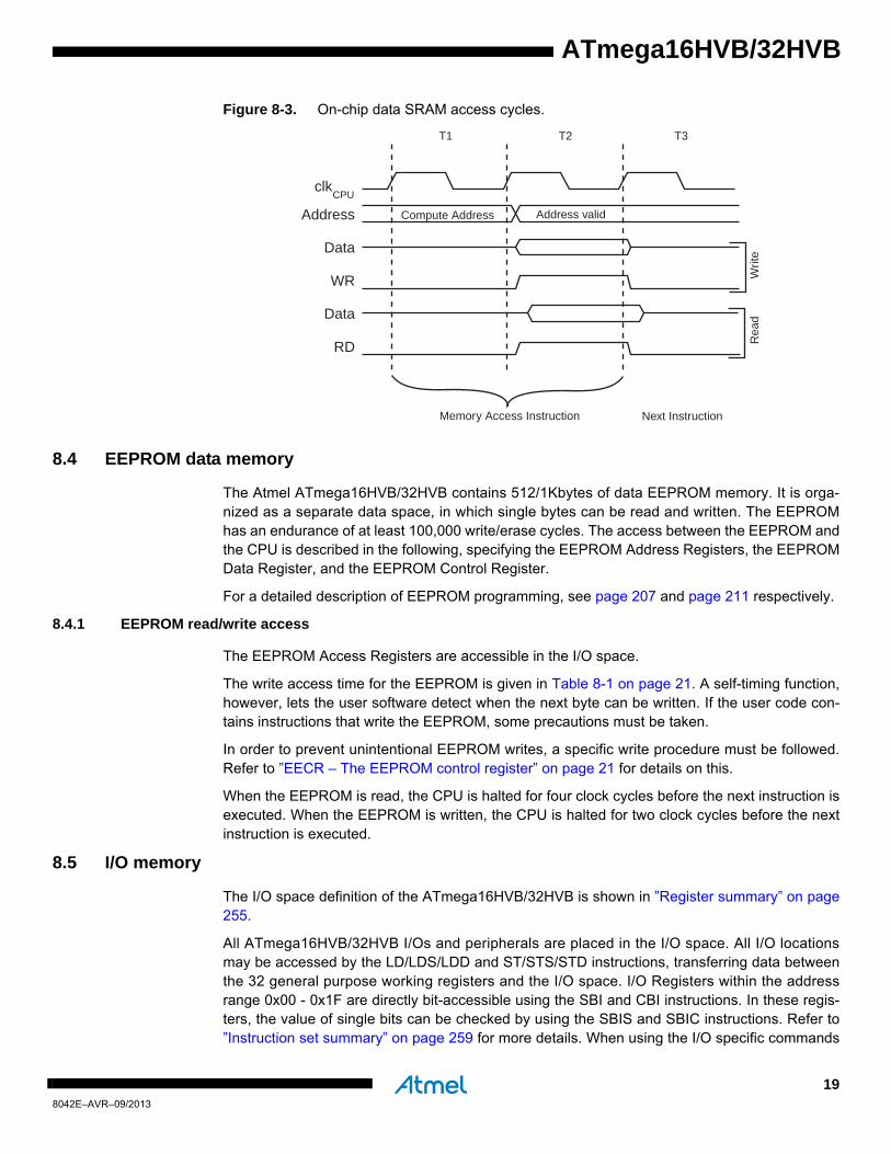
8.3.1 Data memory access times
This section describes the general access timing concepts for internal memory access. Theinternal data SRAM access is performed in two clkCPU cycles as described in Figure 8-3 on page19.
32 Registers64 I/O Registers
Internal SRAM(1K/2K x 8)
0x0000 - 0x001F0x0020 - 0x005F
0x04FF/0x08FF
0x0060 - 0x00FF
Data Memory
160 Ext I/O Reg.0x0100
188042E–AVR–09/2013
ATmega16HVB/32HVB
ATmega16HVB/32HVB
Figure 8-3. On-chip data SRAM access cycles.
8.4 EEPROM data memory
The Atmel ATmega16HVB/32HVB contains 512/1Kbytes of data EEPROM memory. It is orga-nized as a separate data space, in which single bytes can be read and written. The EEPROMhas an endurance of at least 100,000 write/erase cycles. The access between the EEPROM andthe CPU is described in the following, specifying the EEPROM Address Registers, the EEPROMData Register, and the EEPROM Control Register.
For a detailed description of EEPROM programming, see page 207 and page 211 respectively.
8.4.1 EEPROM read/write access
The EEPROM Access Registers are accessible in the I/O space.
The write access time for the EEPROM is given in Table 8-1 on page 21. A self-timing function,however, lets the user software detect when the next byte can be written. If the user code con-tains instructions that write the EEPROM, some precautions must be taken.
In order to prevent unintentional EEPROM writes, a specific write procedure must be followed.Refer to ”EECR – The EEPROM control register” on page 21 for details on this.
When the EEPROM is read, the CPU is halted for four clock cycles before the next instruction isexecuted. When the EEPROM is written, the CPU is halted for two clock cycles before the nextinstruction is executed.
8.5 I/O memory
The I/O space definition of the ATmega16HVB/32HVB is shown in ”Register summary” on page255.
All ATmega16HVB/32HVB I/Os and peripherals are placed in the I/O space. All I/O locationsmay be accessed by the LD/LDS/LDD and ST/STS/STD instructions, transferring data betweenthe 32 general purpose working registers and the I/O space. I/O Registers within the addressrange 0x00 - 0x1F are directly bit-accessible using the SBI and CBI instructions. In these regis-ters, the value of single bits can be checked by using the SBIS and SBIC instructions. Refer to”Instruction set summary” on page 259 for more details. When using the I/O specific commands
clk
WR
RD
Data
Data
Address Address valid
T1 T2 T3
Compute Address
Rea
dW
rite
CPU
Memory Access Instruction Next Instruction
198042E–AVR–09/2013
IN and OUT, the I/O addresses 0x00 - 0x3F must be used. When addressing I/O Registers asdata space using LD and ST instructions, 0x20 must be added to these addresses. The AtmelATmega16HVB/32HVB is a complex microcontroller with more peripheral units than can be sup-ported within the 64 location reserved in Opcode for the IN and OUT instructions. For theExtended I/O space from 0x60 - 0xFF in SRAM, only the ST/STS/STD and LD/LDS/LDD instruc-tions can be used.
For compatibility with future devices, reserved bits should be written to zero if accessed.Reserved I/O memory addresses should never be written.
Some of the status flags are cleared by writing a logical one to them. Note that the CBI and SBIinstructions will only operate on the specified bit, and can therefore be used on registers contain-ing such status flags. The CBI and SBI instructions work with registers 0x00 to 0x1F only.
The I/O and peripherals control registers are explained in later sections.
8.5.1 General purpose I/O registers
The ATmega16HVB/32HVB contains three General Purpose I/O Registers. These registers canbe used for storing any information, and they are particularly useful for storing global variablesand Status Flags. General Purpose I/O Registers within the address range 0x00 - 0x1F aredirectly bit-accessible using the SBI, CBI, SBIS, and SBIC instructions.
8.6 Register description
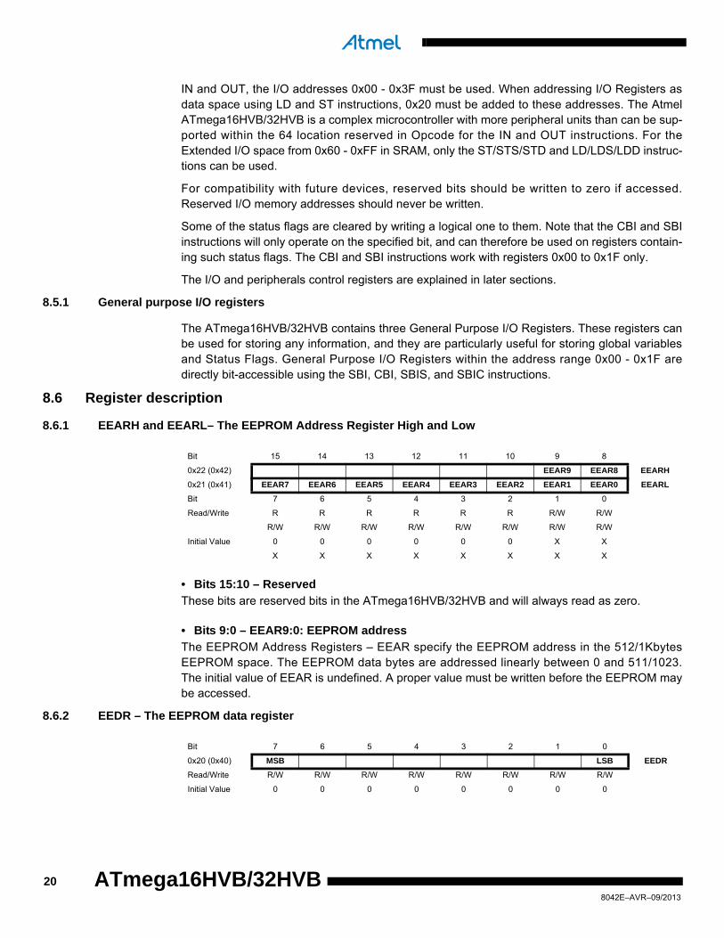
8.6.1 EEARH and EEARL– The EEPROM Address Register High and Low
• Bits 15:10 – Reserved
These bits are reserved bits in the ATmega16HVB/32HVB and will always read as zero.
• Bits 9:0 – EEAR9:0: EEPROM address
The EEPROM Address Registers – EEAR specify the EEPROM address in the 512/1KbytesEEPROM space. The EEPROM data bytes are addressed linearly between 0 and 511/1023.The initial value of EEAR is undefined. A proper value must be written before the EEPROM maybe accessed.
8.6.2 EEDR – The EEPROM data register
Bit 15 14 13 12 11 10 9 8
0x22 (0x42) EEAR9 EEAR8 EEARH
0x21 (0x41) EEAR7 EEAR6 EEAR5 EEAR4 EEAR3 EEAR2 EEAR1 EEAR0 EEARL
Bit 7 6 5 4 3 2 1 0
Read/Write R R R R R R R/W R/W
R/W R/W R/W R/W R/W R/W R/W R/W
Initial Value 0 0 0 0 0 0 X X
X X X X X X X X
Bit 7 6 5 4 3 2 1 0
0x20 (0x40) MSB LSB EEDR
Read/Write R/W R/W R/W R/W R/W R/W R/W R/W
Initial Value 0 0 0 0 0 0 0 0
208042E–AVR–09/2013
ATmega16HVB/32HVB
ATmega16HVB/32HVB
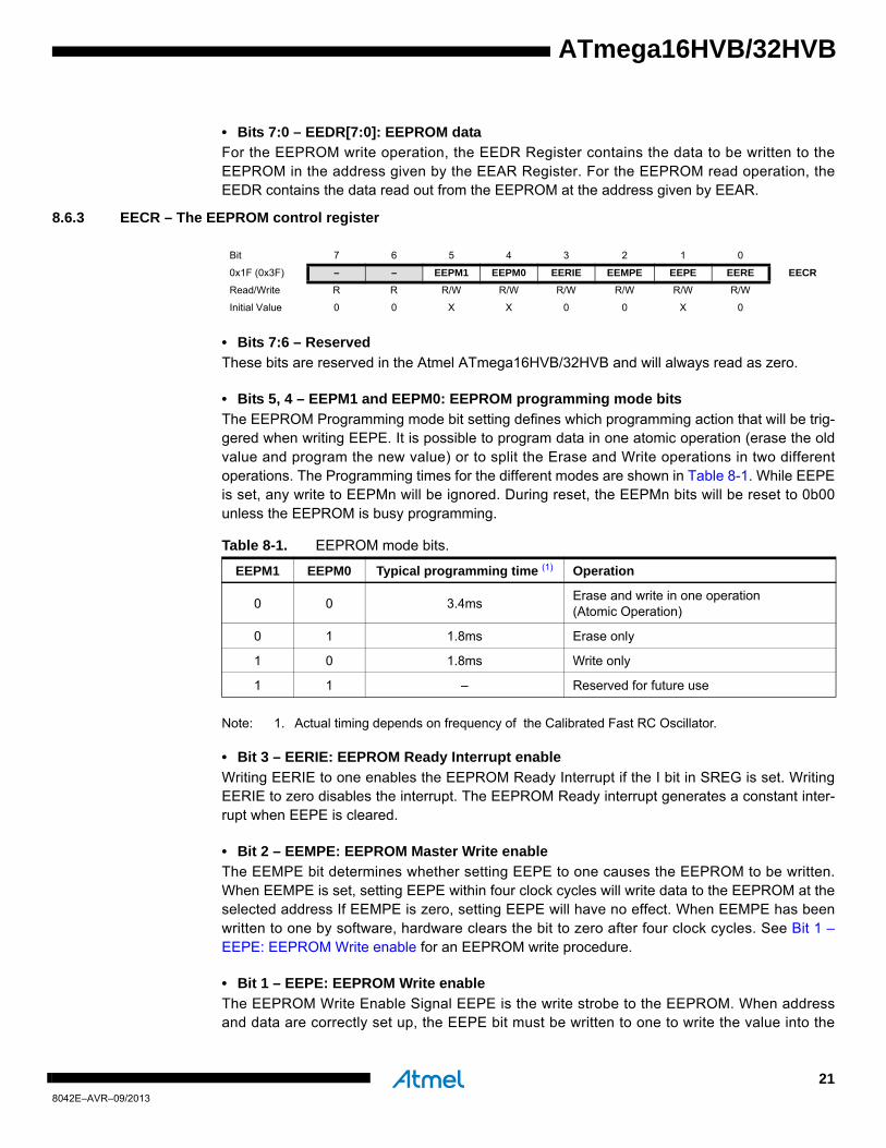
• Bits 7:0 – EEDR[7:0]: EEPROM data
For the EEPROM write operation, the EEDR Register contains the data to be written to theEEPROM in the address given by the EEAR Register. For the EEPROM read operation, theEEDR contains the data read out from the EEPROM at the address given by EEAR.
8.6.3 EECR – The EEPROM control register
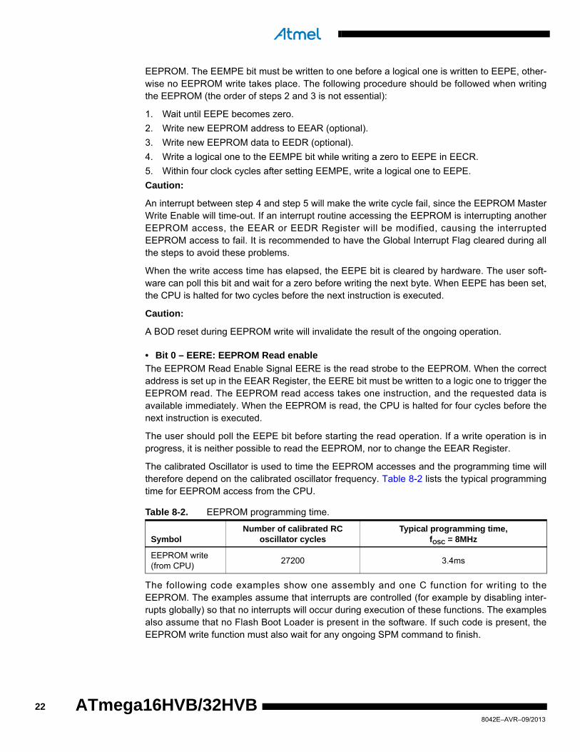
• Bits 7:6 – Reserved
These bits are reserved in the Atmel ATmega16HVB/32HVB and will always read as zero.
• Bits 5, 4 – EEPM1 and EEPM0: EEPROM programming mode bits
The EEPROM Programming mode bit setting defines which programming action that will be trig-gered when writing EEPE. It is possible to program data in one atomic operation (erase the oldvalue and program the new value) or to split the Erase and Write operations in two differentoperations. The Programming times for the different modes are shown in Table 8-1. While EEPEis set, any write to EEPMn will be ignored. During reset, the EEPMn bits will be reset to 0b00unless the EEPROM is busy programming.
Note: 1. Actual timing depends on frequency of the Calibrated Fast RC Oscillator.
• Bit 3 – EERIE: EEPROM Ready Interrupt enable
Writing EERIE to one enables the EEPROM Ready Interrupt if the I bit in SREG is set. WritingEERIE to zero disables the interrupt. The EEPROM Ready interrupt generates a constant inter-rupt when EEPE is cleared.
• Bit 2 – EEMPE: EEPROM Master Write enable
The EEMPE bit determines whether setting EEPE to one causes the EEPROM to be written.When EEMPE is set, setting EEPE within four clock cycles will write data to the EEPROM at theselected address If EEMPE is zero, setting EEPE will have no effect. When EEMPE has beenwritten to one by software, hardware clears the bit to zero after four clock cycles. See Bit 1 –EEPE: EEPROM Write enable for an EEPROM write procedure.
• Bit 1 – EEPE: EEPROM Write enable
The EEPROM Write Enable Signal EEPE is the write strobe to the EEPROM. When addressand data are correctly set up, the EEPE bit must be written to one to write the value into the
Bit 7 6 5 4 3 2 1 0
0x1F (0x3F) – – EEPM1 EEPM0 EERIE EEMPE EEPE EERE EECR
Read/Write R R R/W R/W R/W R/W R/W R/W
Initial Value 0 0 X X 0 0 X 0
Table 8-1. EEPROM mode bits.
EEPM1 EEPM0 Typical programming time (1) Operation
0 0 3.4msErase and write in one operation(Atomic Operation)
0 1 1.8ms Erase only
1 0 1.8ms Write only
1 1 – Reserved for future use
218042E–AVR–09/2013
EEPROM. The EEMPE bit must be written to one before a logical one is written to EEPE, other-wise no EEPROM write takes place. The following procedure should be followed when writingthe EEPROM (the order of steps 2 and 3 is not essential):
1. Wait until EEPE becomes zero.
2. Write new EEPROM address to EEAR (optional).
3. Write new EEPROM data to EEDR (optional).
4. Write a logical one to the EEMPE bit while writing a zero to EEPE in EECR.
5. Within four clock cycles after setting EEMPE, write a logical one to EEPE.
Caution:
An interrupt between step 4 and step 5 will make the write cycle fail, since the EEPROM MasterWrite Enable will time-out. If an interrupt routine accessing the EEPROM is interrupting anotherEEPROM access, the EEAR or EEDR Register will be modified, causing the interruptedEEPROM access to fail. It is recommended to have the Global Interrupt Flag cleared during allthe steps to avoid these problems.
When the write access time has elapsed, the EEPE bit is cleared by hardware. The user soft-ware can poll this bit and wait for a zero before writing the next byte. When EEPE has been set,the CPU is halted for two cycles before the next instruction is executed.
Caution:
A BOD reset during EEPROM write will invalidate the result of the ongoing operation.
• Bit 0 – EERE: EEPROM Read enable
The EEPROM Read Enable Signal EERE is the read strobe to the EEPROM. When the correctaddress is set up in the EEAR Register, the EERE bit must be written to a logic one to trigger theEEPROM read. The EEPROM read access takes one instruction, and the requested data isavailable immediately. When the EEPROM is read, the CPU is halted for four cycles before thenext instruction is executed.
The user should poll the EEPE bit before starting the read operation. If a write operation is inprogress, it is neither possible to read the EEPROM, nor to change the EEAR Register.
The calibrated Oscillator is used to time the EEPROM accesses and the programming time willtherefore depend on the calibrated oscillator frequency. Table 8-2 lists the typical programmingtime for EEPROM access from the CPU.
The following code examples show one assembly and one C function for writing to theEEPROM. The examples assume that interrupts are controlled (for example by disabling inter-rupts globally) so that no interrupts will occur during execution of these functions. The examplesalso assume that no Flash Boot Loader is present in the software. If such code is present, theEEPROM write function must also wait for any ongoing SPM command to finish.
Table 8-2. EEPROM programming time.
SymbolNumber of calibrated RC
oscillator cyclesTypical programming time,
fOSC = 8MHz
EEPROM write (from CPU)
27200 3.4ms
228042E–AVR–09/2013
ATmega16HVB/32HVB

ATmega16HVB/32HVB
The next code examples show assembly and C functions for reading the EEPROM. The exam-ples assume that interrupts are controlled so that no interrupts will occur during execution ofthese functions.
Assembly code example
EEPROM_write:
; Wait for completion of previous write
sbic EECR,EEPE
rjmp EEPROM_write
; Set up address (r18:r17) in address registerout EEARH, r18
out EEARL, r17
; Write data (r16) to data register
out EEDR,r16
; Write logical one to EEMPE
sbi EECR,EEMPE
; Start eeprom write by setting EEPE
sbi EECR,EEPE
ret
C code example
void EEPROM_write(unsigned int uiAddress, unsigned char ucData)
{
/* Wait for completion of previous write */
while(EECR & (1<<EEPE))
;
/* Set up address and data registers */
EEAR = uiAddress;
EEDR = ucData;
/* Write logical one to EEMPE */
EECR |= (1<<EEMPE);
/* Start eeprom write by setting EEPE */
EECR |= (1<<EEPE);
}
238042E–AVR–09/2013

8.6.4 GPIOR2 – General purpose I/O Register 2
8.6.5 GPIOR1 – General purpose I/O Register 1
8.6.6 GPIOR0 – General purpose I/O Register 0
Assembly code example
EEPROM_read:
; Wait for completion of previous write
sbic EECR,EEPE
rjmp EEPROM_read
; Set up address (r18:r17) in address register
out EEARH, r18
out EEARL, r17
; Start eeprom read by writing EERE
sbi EECR,EERE
; Read data from data register
in r16,EEDR
ret
C code example
unsigned char EEPROM_read(unsigned int uiAddress)
{
/* Wait for completion of previous write */
while(EECR & (1<<EEPE))
;
/* Set up address register */
EEAR = uiAddress;
/* Start eeprom read by writing EERE */
EECR |= (1<<EERE);
/* Return data from data register */
return EEDR;
}
Bit 7 6 5 4 3 2 1 0
0x2B (0x4B) MSB LSB GPIOR2
Read/Write R/W R/W R/W R/W R/W R/W R/W R/W
Initial Value 0 0 0 0 0 0 0 0
Bit 7 6 5 4 3 2 1 0
0x2A (0x4A) MSB LSB GPIOR1
Read/Write R/W R/W R/W R/W R/W R/W R/W R/W
Initial Value 0 0 0 0 0 0 0 0
Bit 7 6 5 4 3 2 1 0
0x1E (0x3E) MSB LSB GPIOR0
Read/Write R/W R/W R/W R/W R/W R/W R/W R/W
Initial Value 0 0 0 0 0 0 0 0
248042E–AVR–09/2013
ATmega16HVB/32HVB
ATmega16HVB/32HVB
9. System clock and clock options
9.1 Clock systems and their distribution
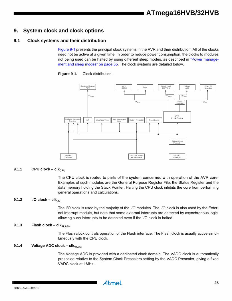
Figure 9-1 presents the principal clock systems in the AVR and their distribution. All of the clocksneed not be active at a given time. In order to reduce power consumption, the clocks to modulesnot being used can be halted by using different sleep modes, as described in ”Power manage-ment and sleep modes” on page 35. The clock systems are detailed below.
Figure 9-1. Clock distribution.
9.1.1 CPU clock – clkCPU
The CPU clock is routed to parts of the system concerned with operation of the AVR core.Examples of such modules are the General Purpose Register File, the Status Register and thedata memory holding the Stack Pointer. Halting the CPU clock inhibits the core from performinggeneral operations and calculations.
9.1.2 I/O clock – clkI/O
The I/O clock is used by the majority of the I/O modules. The I/O clock is also used by the Exter-nal Interrupt module, but note that some external interrupts are detected by asynchronous logic,allowing such interrupts to be detected even if the I/O clock is halted.
9.1.3 Flash clock – clkFLASH
The Flash clock controls operation of the Flash interface. The Flash clock is usually active simul-taneously with the CPU clock.
9.1.4 Voltage ADC clock – clkVADC
The Voltage ADC is provided with a dedicated clock domain. The VADC clock is automaticallyprescaled relative to the System Clock Prescalers setting by the VADC Prescaler, giving a fixedVADC clock at 1MHz.
Ultra Low Power RC Oscillator
Watchdog Timer Battery Protection Reset Logic
CPUCORE
RAMFLASH and
EEPROMVoltage
ADCOther I/OModules
Coulomb CounterADC
AVRClock Control
Fast RCOscillator
clkCPU
clkFLASH clk
VADC
clkI/O
1/4
System ClockPrescaler
VADCPrescaler
Oscillator SamplingInterface
Slow RCOscillator
clkCCADC
TWI Disconnect delay
258042E–AVR–09/2013
9.1.5 Coulomb counter ADC clock - clkCCADC
The Coulomb Counter ADC is provided with a dedicated clock domain. This allows operating theCoulomb Counter ADC in low power modes like Power-save for continuous currentmeasurements.
9.1.6 Watchdog timer and battery protection clock
The Watchdog Timer and Battery Protection are provided with a dedicated clock domain. Thisallows operation in all modes except Power-off. It also allows very low power operation by utiliz-ing an Ultra Low Power RC Oscillator dedicated to this purpose.
9.2 Clock sources
The following section describes the clock sources available in the device. The clocks are input tothe AVR clock generator, and routed to the appropriate modules.
The Atmel ATmega16HVB/32HVB has three on-board oscillators used to clock the internal logic.Table 9-1 shows the clock sources and their usage.
9.2.1 Calibrated Fast RC oscillator
The calibrated Fast RC Oscillator by default provides a 8.0MHz clock. The frequency is nominalvalue at 25C. This clock will operate with no external components. During reset, hardwareloads the calibration byte into the FOSCCAL Register and thereby automatically calibrates theFast RC Oscillator. At 25C, this calibration gives a frequency of 8MHz ±1%. The oscillator canbe calibrated to any frequency in the range 7.3MHz - 8.1MHz by changing the FOSCCAL regis-ter. For more information on the pre-programmed calibration value, see the section ”Reading thesignature row from software” on page 195. Note that the frequency of the system clock is givenby the ”System clock prescaler” on page 28.
When this Oscillator is selected, start-up times are determined by the SUT Fuses as shown inTable 9-2.
Table 9-1. Available clock sources.
Clock source Usage
Calibrated fast RC oscillator The clock source for the CPU, I/O, Flash, and Voltage ADC
Ultra low power RC oscillatorThe clock source for the Watchdog Timer, Battery Protection, Bandgap Buffer Short Circuit Detector, and SMBus Connect/Disconnect
Slow RC oscillatorUsed by the Coulomb Counter ADC and Oscillator Sampling Interface (OSI)
Table 9-2. Start-up times for the calibrated Fast RC Oscillator clock selection.
SUT2:0Start-up time from
power-save Additional delay from reset, typical values (2)
000 6 CK 14 CK + 4ms
001 6 CK 14 CK + 8ms
010 6 CK 14 CK + 16ms
011 6 CK 14 CK + 32ms
100 6 CK 14 CK + 64ms
268042E–AVR–09/2013
ATmega16HVB/32HVB

ATmega16HVB/32HVB
Notes: 1. The device is shipped with this option selected.2. The actual value of the added, selectable 4ms - 512ms delay depends on the actual frequency
of the “Ultra Low Power RC oscillator” . See Table 9-3 on page 28 and ”Electrical characteris-tics” on page 225.
9.2.2 Slow RC oscillator
The Slow RC Oscillator provides a 131kHz clock (typical value, refer to section ”Electrical char-acteristics” on page 225). This oscillator provides the clock for the CC-ADC module. It can alsobe used as a timing reference for run-time calibration of the Fast RC Oscillator and for accu-rately determining the actual ULP Oscillator frequency, refer to ”OSI – Oscillator samplinginterface” on page 29 for details.
To provide good accuracy when used as a timing reference, the Slow RC Oscillator has calibra-tion bytes stored in the signature address space, refer to section ”Reading the signature rowfrom software” on page 195 for details. The actual clock period of the Slow RC Oscillator in s asa function of temperature is given by:
where T is the die temperature in Kelvin and THOT is the calibration temperature stored in the sig-nature row. The die temperature can be found using the Voltage ADC, refer to section ”VoltageADC – 7-channel general purpose 12-bit Sigma-Delta ADC” on page 116 for details.
9.2.3 Ultra Low Power RC oscillator
The Ultra Low Power RC Oscillator (ULP Oscillator) provides a 128kHz clock (typical value, referto section ”Electrical characteristics” on page 225). This oscillator provides the clock for theWatchdog Timer and Battery Protection modules. The actual ULP Oscillator frequency dependson process variations and temperature, see ”Electrical characteristics” on page 225. The Oscilla-tor is automatically enabled in all operational modes. It is also enabled during reset. There arethree alternative methods for determining the actual clock period of the ULP Oscillator:
1. To determine the accurate clock period as a function of die temperature, if needed by the application, the Oscillator Sampling Interface should be used. Refer to section ”OSI – Oscillator sampling interface” on page 29 for details.
2. An alternative method to determine the accurate clock period as a function of die temper-ature, is to read calibration bytes from the signature address space and calculate the clock period as a function of die temperature, refer to section ”Reading the signature row from software” on page 195 for details. The actual clock period of the ULP RC Oscillator in μs as a function of temperature is given by:
101 6 CK 14 CK + 128ms
110 6 CK 14 CK + 256ms
111 (1) 6 CK 14 CK + 512ms
Table 9-2. Start-up times for the calibrated Fast RC Oscillator clock selection. (Continued)
SUT2:0Start-up time from
power-save Additional delay from reset, typical values (2)
Slow RC periodSlow RC word - Slow RC temp prediction word
(T THOT)–
64---------------------------
1024------------------------------------------------------------------------------------------------------------------------------------------------------------=
ULP RC periodULP RC word - ULP RC temp prediction word
(T THOT)–
64---------------------------
1024---------------------------------------------------------------------------------------------------------------------------------------------------------=
278042E–AVR–09/2013

where T is the die temperature in Kelvin and THOT is the calibration temperature stored inthe Signature row. The die temperature can be found using the Voltage ADC, refer to section”Voltage ADC – 7-channel general purpose 12-bit Sigma-Delta ADC” on page 116 fordetails.
3. To determine a fixed value for the actual clock period independent of the die temperature, for example to determine the best setting of the Battery Protection timing, use the calibra-tion byte ULP_RC_FRQ stored in the signature address space, refer to section ”Reading the signature row from software” on page 195 for details.
9.3 Clock startup sequence
When the CPU wakes up from Power-save, the CPU clock source is used to time the start-up,ensuring a stable clock before instruction execution starts. When the CPU starts from reset,there is an additional delay allowing the voltage regulator to reach a stable level before com-mencing normal operation. The Ultra Low Power RC Oscillator is used for timing this real-timepart of the start-up time. Start-up times are determined by the SUT Fuses as shown in Table 9-2on page 26. The number of Ultra Low Power RC Oscillator cycles used for each time-out isshown in Table 9-3.
Note: 1. The actual value depends on the actual clock period of the Ultra Low Power RC Oscillator, refer to ”Ultra Low Power RC oscillator” on page 27 for details.
9.4 Clock output
The CPU clock divided by two can be output to the PB1 pin. The CPU can enable the clock out-put function by setting the CKOE bit in the MCU Control Register. The clock will not run in anysleep modes.
9.5 System clock prescaler
The Atmel ATmega16HVB/32HVB has a System Clock Prescaler, used to prescale the Cali-brated Fast RC Oscillator. The system clock can be divided by setting the ”CLKPR – ClockPrescale Register” on page 32, and this enables the user to decrease or increase the systemclock frequency as the requirement for power consumption and processing power changes. Thissystem clock will affect the clock frequency of the CPU and all synchronous peripherals. clkI/O,clkCPU and clkFLASH are divided by a factor as shown in Table 9-4 on page 33.
When switching between prescaler settings, the System Clock Prescaler ensures that noglitches occurs in the clock system. It also ensures that no intermediate frequency is higher than
Table 9-3. Number of Ultra Low Power RC oscillator cycles.
Typical time-out (1) Number of cycles
4ms 512
8ms 1K
16ms 2K
32ms 4K
64ms 8K
128ms 16K
256ms 32K
512ms 64K
288042E–AVR–09/2013
ATmega16HVB/32HVB
ATmega16HVB/32HVB
neither the clock frequency corresponding to the previous setting, nor the clock frequency corre-sponding to the new setting.
The ripple counter that implements the prescaler runs at the frequency of the undivided clock,and may be faster than the CPU's clock frequency. It is not possible to determine the state of theprescaler, and the exact time it takes to switch from one clock division to the other cannot beexactly predicted. From the time the CLKPS values are written, it takes between T1 + T2 and T1+ 2×T2 before the new clock frequency is active. In this interval, two active clock edges are pro-duced. Here, T1 is the previous clock period, and T2 is the period corresponding to the newprescaler setting.
To avoid unintentional changes of clock frequency, a special write procedure must be followedto change the CLKPS bits:
1. Write the Clock Prescaler Change Enable (CLKPCE) bit to one and all other bits in CLKPR to zero.
2. Within four cycles, write the desired value to CLKPS while writing a zero to CLKPCE.
Interrupts must be disabled when changing prescaler setting to make sure the write procedure isnot interrupted.
9.6 VADC clock prescaler
The VADC clock will be automatically prescaled relative to the System Clock Prescaler settings,see ”System clock prescaler” on page 28. Depending on the Clock Prescale Select bits,CLKPS1..0, the VADC clock, clkVADC, will be prescaled by eight, four, two or one as shown inTable 9-5 on page 33.
9.7 OSI – Oscillator sampling interface
9.7.1 Features
• Runtime selectable oscillator input (Slow RC or ULP RC oscillator)
• Seven bit prescaling of the selected oscillator
• Software read access to the phase of the prescaled clock
• Input capture trigger source for Timer/Counter0
9.7.2 Overview
The Oscillator Sampling Interface (OSI) enables sampling of the Slow RC and Ultra Low PowerRC (ULP) oscillators in Atmel ATmega16HVB/32HVB. OSI can be used to calibrate the Fast RCOscillator runtime with high accuracy. OSI can also provide an accurate reference for compen-sating the ULP Oscillator frequency drift.
The prescaled oscillator phase can be continuously read by the CPU through the OSICSR regis-ter. In addition, the input capture function of Timer/Counter0 can be set up to trigger on the risingedge of the prescaled clock. This enables accurate measurements of the oscillator frequenciesrelative to the Fast RC Oscillator.
A simplified block diagram of the Oscillator Sampling Interface is shown in Figure 9-2 on page30.
298042E–AVR–09/2013

Figure 9-2. Oscillator sampling interface block diagram.
The osi_posedge signal pulses on each rising edge of the prescaled clock. This signal is notdirectly accessible by the CPU, but can be used to trigger the input capture function ofTimer/Counter0. Using OSI in combination with the input capture function of Timer/Counter0facilitates accurate measurement of the oscillator frequencies with a minimum of CPU calcula-tion. Refer to ”Timer/Counter (T/C0,T/C1)” on page 82 for details on how to enable the InputCapture function.
osi_posedge
Databus
Ultra Low Power RC Oscillator
Slow RC Oscillator
OS
CIL
LA
TO
R S
EL
EC
T
7 bit prescalerEdge
Detector
OSISEL0
OSICSR
Fast RC Oscillator
308042E–AVR–09/2013
ATmega16HVB/32HVB
ATmega16HVB/32HVB
9.7.3 Usage
The Slow RC oscillator represents a highly predictable and accurate clock source over the entiretemperature range and provides an excellent reference for calibrating the Fast RC oscillator run-time. Typically, runtime calibration is needed to provide an accurate Fast RC frequency forasynchronous serial communication in the complete temperature range.
The Slow RC frequency at 85C and the Slow RC temperature coefficient are stored in the sig-nature row. These characteristics can be used to calculate the actual Slow RC clock period at agiven temperature with high precision. Refer to ”Slow RC oscillator” on page 27 for details.
By measuring the number of CPU cycles of one or more prescaled Slow RC clock periods, theactual Fast RC oscillator clock period can be determined. The Fast RC clock period can then beadjusted by writing to the FOSCCAL register. The new Fast RC clock period after calibrationshould be verified by repeating the measurement and repeating the calibration if necessary. TheFast RC clock period as a function of the Slow RC clock period is given by:
where n is the number of prescaled Slow RC periods that is used in the measurement. Usingmore prescaled Slow RC periods decreases the measurement error, but increases the time con-sumed for calibration. Note that the Slow RC Oscillator needs very short time to stabilize afterbeing enabled by the OSI module. Hence, the calibration algorithm may use the time betweenthe first and second osi_posedge as time reference for calculations.
Another usage of OSI is determining the ULP frequency accurately. The ULP frequency at 85Cand the ULP temperature coefficient are stored in the signature row, allowing the ULP frequencyto be calculated directly. However, the ULP frequency is less predictable over temperature thanthe Slow RC oscillator frequency, therefore a more accurate result can be obtained by calculat-ing the ratio between the Slow RC and ULP oscillators. This is done by sampling both the ULPand Slow RC oscillators and comparing the results. When the ratio is known, the actual ULP fre-quency can be determined with high accuracy. The ULP RC clock period as a function of theSlow RC clock period is given by:
where n is the number of prescaled ULP RC and Slow RC periods that is used in the measure-ment. Using more prescaled ULP RC and Slow RC periods decreases the measurement error,but increases the time consumed for calibration. Note that the FOSCCAL register must be keptat a constant value during this operation to ensure accurate results.
These clock period calculations should be performed again when there is a significant change indie temperature since the previous calculation. The die temperature can be found using the Volt-age ADC, refer to section ”Voltage ADC – 7-channel general purpose 12-bit Sigma-Delta ADC”on page 116 for details.
TFastRC TSlowRC128 n
number of CPU cycles in n prescaled Slow RC periods-------------------------------------------------------------------------------------------------------------------------------------------------=
TULPRC TSlowRCnumber of CPU cycles in n prescaled ULP RC periodsnumber of CPU cycles in n prescaled Slow RC periods-------------------------------------------------------------------------------------------------------------------------------------------------=
318042E–AVR–09/2013
9.8 Register description
9.8.1 FOSCCAL – Fast RC oscillator Calibration Register
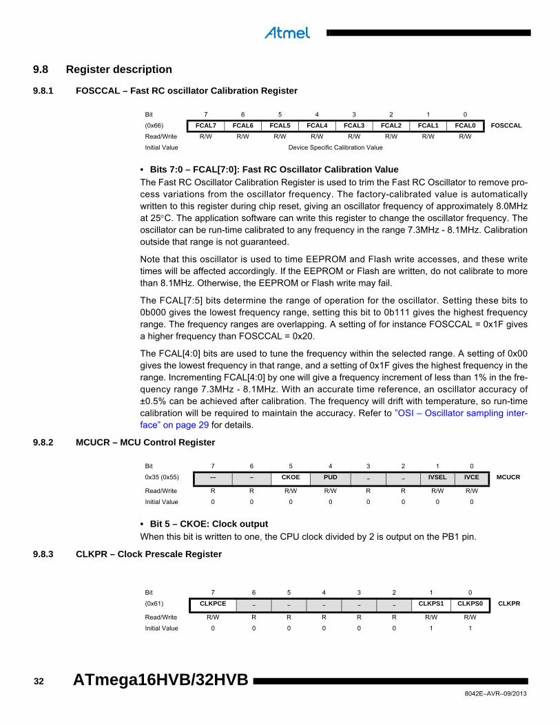
• Bits 7:0 – FCAL[7:0]: Fast RC Oscillator Calibration Value
The Fast RC Oscillator Calibration Register is used to trim the Fast RC Oscillator to remove pro-cess variations from the oscillator frequency. The factory-calibrated value is automaticallywritten to this register during chip reset, giving an oscillator frequency of approximately 8.0MHzat 25C. The application software can write this register to change the oscillator frequency. Theoscillator can be run-time calibrated to any frequency in the range 7.3MHz - 8.1MHz. Calibrationoutside that range is not guaranteed.
Note that this oscillator is used to time EEPROM and Flash write accesses, and these writetimes will be affected accordingly. If the EEPROM or Flash are written, do not calibrate to morethan 8.1MHz. Otherwise, the EEPROM or Flash write may fail.
The FCAL[7:5] bits determine the range of operation for the oscillator. Setting these bits to0b000 gives the lowest frequency range, setting this bit to 0b111 gives the highest frequencyrange. The frequency ranges are overlapping. A setting of for instance FOSCCAL = 0x1F givesa higher frequency than FOSCCAL = 0x20.
The FCAL[4:0] bits are used to tune the frequency within the selected range. A setting of 0x00gives the lowest frequency in that range, and a setting of 0x1F gives the highest frequency in therange. Incrementing FCAL[4:0] by one will give a frequency increment of less than 1% in the fre-quency range 7.3MHz - 8.1MHz. With an accurate time reference, an oscillator accuracy of±0.5% can be achieved after calibration. The frequency will drift with temperature, so run-timecalibration will be required to maintain the accuracy. Refer to ”OSI – Oscillator sampling inter-face” on page 29 for details.
9.8.2 MCUCR – MCU Control Register
• Bit 5 – CKOE: Clock output
When this bit is written to one, the CPU clock divided by 2 is output on the PB1 pin.
9.8.3 CLKPR – Clock Prescale Register
Bit 7 6 5 4 3 2 1 0
(0x66) FCAL7 FCAL6 FCAL5 FCAL4 FCAL3 FCAL2 FCAL1 FCAL0 FOSCCAL
Read/Write R/W R/W R/W R/W R/W R/W R/W R/W
Initial Value Device Specific Calibration Value
Bit 7 6 5 4 3 2 1 0
0x35 (0x55) -– – CKOE PUD – – IVSEL IVCE MCUCR
Read/Write R R R/W R/W R R R/W R/W
Initial Value 0 0 0 0 0 0 0 0
Bit 7 6 5 4 3 2 1 0
(0x61) CLKPCE – – – – – CLKPS1 CLKPS0 CLKPR
Read/Write R/W R R R R R R/W R/W
Initial Value 0 0 0 0 0 0 1 1
328042E–AVR–09/2013
ATmega16HVB/32HVB
ATmega16HVB/32HVB
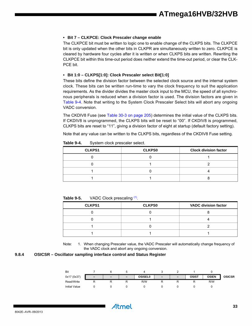
• Bit 7 – CLKPCE: Clock Prescaler change enable
The CLKPCE bit must be written to logic one to enable change of the CLKPS bits. The CLKPCEbit is only updated when the other bits in CLKPR are simultaneously written to zero. CLKPCE iscleared by hardware four cycles after it is written or when CLKPS bits are written. Rewriting theCLKPCE bit within this time-out period does neither extend the time-out period, or clear the CLK-PCE bit.
• Bit 1:0 – CLKPS[1:0]: Clock Prescaler select Bit[1:0]
These bits define the division factor between the selected clock source and the internal systemclock. These bits can be written run-time to vary the clock frequency to suit the applicationrequirements. As the divider divides the master clock input to the MCU, the speed of all synchro-nous peripherals is reduced when a division factor is used. The division factors are given inTable 9-4. Note that writing to the System Clock Prescaler Select bits will abort any ongoingVADC conversion.
The CKDIV8 Fuse (see Table 30-3 on page 205) determines the initial value of the CLKPS bits.If CKDIV8 is unprogrammed, the CLKPS bits will be reset to “00”. If CKDIV8 is programmed,CLKPS bits are reset to “11”, giving a division factor of eight at startup (default factory setting).
Note that any value can be written to the CLKPS bits, regardless of the CKDIV8 Fuse setting.
Note: 1. When changing Prescaler value, the VADC Prescaler will automatically change frequency of the VADC clock and abort any ongoing conversion.
9.8.4 OSICSR – Oscillator sampling interface control and Status Register
Table 9-4. System clock prescaler select.
CLKPS1 CLKPS0 Clock division factor
0 0 1
0 1 2
1 0 4
1 1 8
Table 9-5. VADC Clock prescaling (1).
CLKPS1 CLKPS0 VADC division factor
0 0 8
0 1 4
1 0 2
1 1 1
Bit 7 6 5 4 3 2 1 0
0x17 (0x37) – – – OSISEL0 – – OSIST OSIEN OSICSR
Read/Write R R R R/W R R R R/W
Initial Value 0 0 0 0 0 0 0 0
338042E–AVR–09/2013
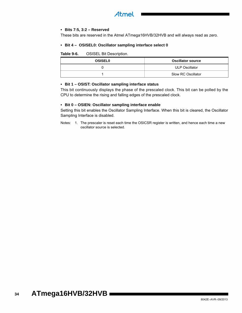
• Bits 7:5, 3:2 – Reserved
These bits are reserved in the Atmel ATmega16HVB/32HVB and will always read as zero.
• Bit 4 – OSISEL0: Oscillator sampling interface select 0
• Bit 1 – OSIST: Oscillator sampling interface status
This bit continuously displays the phase of the prescaled clock. This bit can be polled by theCPU to determine the rising and falling edges of the prescaled clock.
• Bit 0 – OSIEN: Oscillator sampling interface enable
Setting this bit enables the Oscillator Sampling Interface. When this bit is cleared, the OscillatorSampling Interface is disabled.
Notes: 1. The prescaler is reset each time the OSICSR register is written, and hence each time a new oscillator source is selected.
Table 9-6. OSISEL Bit Description.
OSISEL0 Oscillator source
0 ULP Oscillator
1 Slow RC Oscillator
348042E–AVR–09/2013
ATmega16HVB/32HVB

ATmega16HVB/32HVB
10. Power management and sleep modes
Sleep modes enable the application to shut down unused modules in the MCU, thereby savingpower. The AVR provides various sleep modes allowing the user to tailor the power consump-tion to the application’s requirements.
10.1 Sleep modes
Figure 9-1 on page 25 presents the different clock systems in the Atmel ATmega16HVB/32HVB,and their distribution. The figure is helpful in selecting an appropriate sleep mode. The differentsleep modes and their wake up sources is summarized in Table 10-1, and Figure 10-1 on page36 shows a sleep mode state diagram.
Notes: 1. Discharge FET must be switched off for Charge Detect to be active.2. When waking from Power-off the Charger Detect will generate a Power-on Reset (POR). From other sleep modes a charger
detect interrupt will wake-up chip.
To enter any of the sleep modes, the SE bit in SMCR, see ”SMCR – Sleep Mode Control Regis-ter” on page 39, must be written to logic one and a SLEEP instruction must be executed. TheSM2..0 bits in the SMCR Register select which sleep mode will be activated by the SLEEPinstruction. See Table 10-3 on page 40 for a summary.
If an enabled interrupt occurs while the MCU is in a sleep mode, the MCU wakes up. The MCUis then halted for four cycles in addition to the start-up time, executes the interrupt routine, andresumes execution from the instruction following SLEEP. The contents of the register file andSRAM are unaltered when the device wakes up from any sleep mode except Power-off. If areset occurs during sleep mode, the MCU wakes up and executes from the Reset Vector.
Table 10-1. Wake-up Sources for Sleep Modes.
Mode
Wake-up sources
Ban
dg
ap
bu
ffer
sho
rt c
ircu
it d
etec
tio
n
Wa
ke-u
p o
nre
gu
lar
curr
ent
Bat
tery
pro
tect
ion
inte
rru
pts
Ext
ern
al i
nte
rru
pts
WD
T
SP
M/E
EP
RO
M r
ead
y
CC
-AD
C
V-A
DC
Oth
er
I/O
Ch
arg
er d
etec
t (1
)(2)
SM
Bu
s ad
dre
ss m
atch
an
db
us
co
nn
ect/
dis
con
nec
t
Vo
ltag
e re
gu
lato
r w
arn
ing
Idle X X X X X X X X X X X X
ADC noise reduction X X X X X X X X X X X
Power-save X X X X X X X X
Power-off X
358042E–AVR–09/2013

Figure 10-1. Sleep mode state diagram.
.
RESET
Active
Power-off
Power-save
Interrupt
Sleep
Reset From all StatesExcept Power-on Reset
Reset Time-out
Sleepor
Black-outDetection
Charger Connected
Idle
Interrupt
Sleep
Black-outDetection
Black-outDetection
ADC NRM
Black-outDetection
SleepInterrupt
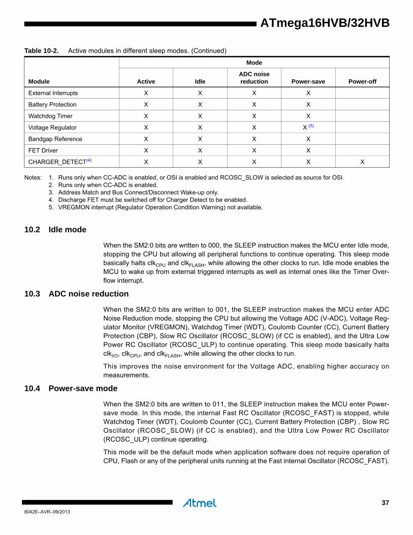
Table 10-2. Active modules in different sleep modes.
Module
Mode
Active IdleADC noisereduction Power-save Power-off
RCOSC_FAST X X X X
RCOSC_ULP X X X X
RCOSC_SLOW X (1) X (1) X (2) X (2)
OSI X X
CPU X
Flash X
8-bit Timer/16-bit Timer X X
TWI/SMBus X X X (3) X (3)
SPI X X
V-ADC X X X
CC-ADC X X X X
368042E–AVR–09/2013
ATmega16HVB/32HVB
ATmega16HVB/32HVB
Notes: 1. Runs only when CC-ADC is enabled, or OSI is enabled and RCOSC_SLOW is selected as source for OSI.2. Runs only when CC-ADC is enabled.3. Address Match and Bus Connect/Disconnect Wake-up only.4. Discharge FET must be switched off for Charger Detect to be enabled.5. VREGMON interrupt (Regulator Operation Condition Warning) not available.
10.2 Idle mode
When the SM2:0 bits are written to 000, the SLEEP instruction makes the MCU enter Idle mode,stopping the CPU but allowing all peripheral functions to continue operating. This sleep modebasically halts clkCPU and clkFLASH, while allowing the other clocks to run. Idle mode enables theMCU to wake up from external triggered interrupts as well as internal ones like the Timer Over-flow interrupt.
10.3 ADC noise reduction
When the SM2:0 bits are written to 001, the SLEEP instruction makes the MCU enter ADCNoise Reduction mode, stopping the CPU but allowing the Voltage ADC (V-ADC), Voltage Reg-ulator Monitor (VREGMON), Watchdog Timer (WDT), Coulomb Counter (CC), Current BatteryProtection (CBP), Slow RC Oscillator (RCOSC_SLOW) (if CC is enabled), and the Ultra LowPower RC Oscillator (RCOSC_ULP) to continue operating. This sleep mode basically haltsclkI/O, clkCPU, and clkFLASH, while allowing the other clocks to run.
This improves the noise environment for the Voltage ADC, enabling higher accuracy onmeasurements.
10.4 Power-save mode
When the SM2:0 bits are written to 011, the SLEEP instruction makes the MCU enter Power-save mode. In this mode, the internal Fast RC Oscillator (RCOSC_FAST) is stopped, whileWatchdog Timer (WDT), Coulomb Counter (CC), Current Battery Protection (CBP) , Slow RCOscillator (RCOSC_SLOW) (if CC is enabled), and the Ultra Low Power RC Oscillator(RCOSC_ULP) continue operating.
This mode will be the default mode when application software does not require operation ofCPU, Flash or any of the peripheral units running at the Fast internal Oscillator (RCOSC_FAST).
External Interrupts X X X X
Battery Protection X X X X
Watchdog Timer X X X X
Voltage Regulator X X X X (5)
Bandgap Reference X X X X
FET Driver X X X X
CHARGER_DETECT(4) X X X X X
Table 10-2. Active modules in different sleep modes. (Continued)
Module
Mode
Active IdleADC noisereduction Power-save Power-off
378042E–AVR–09/2013

If the current through the sense resistor is so small that the Coulomb Counter cannot measure itaccurately, Regular Current detection should be enabled to reduce power consumption. TheWDT keeps accurately track of the time so that battery self discharge can be calculated.
Note that if a level triggered interrupt is used for wake-up from Power-save mode, the changedlevel must be held for some time to wake up the MCU. Refer to ”External interrupts” on page 58for details.
When waking up from Power-save mode, there is a delay from the wake-up condition occursuntil the wake-up becomes effective. This allows the clock to restart and become stable afterhaving been stopped. The wake-up period is defined in ”Clock sources” on page 26.
10.5 Power-off mode
When the SM2..0 bits are written to 100 and the SE bit is set, the SLEEP instruction makes theCPU shut down the Voltage Regulator, leaving only the Charger Detect Circuitry operational. Toensure that the MCU enters Power-off mode only when intended, the SLEEP instruction must beexecuted within 4 clock cycles after the SM2..0 bits are written. The MCU will reset when return-ing from Power-off mode.
Note: 1. Before entering Power-off sleep mode, interrupts should be disabled by software. Otherwise interrupts may prevent the SLEEP instruction from being executed within the time limit.
10.6 Power Reduction Register
The Power Reduction Register (PRR), see ”PRR0 – Power Reduction Register 0” on page 40,provides a method to stop the clock to individual peripherals to reduce power consumption. Thecurrent state of the peripheral is frozen and the I/O registers can not be read or written.Resources used by the peripheral when stopping the clock will remain occupied, hence theperipheral should in most cases be disabled before stopping the clock. Waking up a module,which is done by clearing the bit in PRR, puts the module in the same state as before shutdown.
Module shutdown can be used in Idle mode and Active mode to significantly reduce the overallpower consumption. In all other sleep modes, the clock is already stopped.
10.7 Minimizing power consumption
There are several issues to consider when trying to minimize the power consumption in an AVRcontrolled system. In general, sleep modes should be used as much as possible, and the sleepmode should be selected so that as few as possible of the device’s functions are operating. Allfunctions not needed should be disabled. In particular, the following modules may need specialconsideration when trying to achieve the lowest possible power consumption.
10.7.1 Watchdog Timer
If the Watchdog Timer is not needed in the application, the module should be turned off. If theWatchdog Timer is enabled, it will be enabled in all sleep modes except Power-off. The Watch-dog Timer current consumption is significant only in Power-save mode. Refer to ”Watchdogtimer” on page 46 for details on how to configure the Watchdog Timer.
10.7.2 Port pins
When entering a sleep mode, all port pins should be configured to use minimum power. Themost important is then to ensure that no pins drive resistive loads. In sleep modes where boththe I/O clock (clkI/O) and the ADC clock (clkADC) are stopped, the input buffers of the device willbe disabled. This ensures that no power is consumed by the input logic when not needed. In
388042E–AVR–09/2013
ATmega16HVB/32HVB

ATmega16HVB/32HVB
some cases, the input logic is needed for detecting wake-up conditions, and it will then beenabled. Refer to the section ”Digital input enable and sleep modes” on page 71 for details onwhich pins are enabled. If the input buffer is enabled and the input signal is left floating or havean analog signal level close to VREG/2, the input buffer will use excessive power.
For analog input pins, the digital input buffer should be disabled at all times. An analog signallevel close to VREG/2 on an input pin can cause significant current even in active mode. Digitalinput buffers can be disabled by writing to the Digital Input Disable Register. Refer to ”DIDR0 –Digital Input Disable Register 0” on page 121 for details.
10.7.3 On-chip debug system
A programmed DWEN Fuse enables some parts of the clock system to be running in all sleepmodes. This will increase the power consumption while in sleep. Thus, the DWEN Fuse shouldbe disabled when debugWire is not used.
10.7.4 Battery protection
If one of the Battery Protection features is not needed by the application, this feature should bedisabled, see ”BPCR – Battery Protection Control Register” on page 138. The current consump-tion in the Battery Protection circuitry is only significant in Power-save mode. Disabling bothFETs will automatically disable the Battery Protection module in order to save power. The band-gap reference should always be enabled whenever Battery Protection is enabled.
10.7.5 Voltage ADC
If enabled, the V-ADC will consume power independent of sleep mode. To save power, the V-ADC should be disabled when not used, and before entering Power-save sleep mode. See”Voltage ADC – 7-channel general purpose 12-bit Sigma-Delta ADC” on page 116 for details onV-ADC operation.
10.7.6 Coulomb counter
If enabled, the CC-ADC will consume power independent of sleep mode. To save power, theCC-ADC should be disabled when not used, or set in Regular Current detection mode. See”Coulomb counter – Dedicated fuel gauging Sigma-Delta ADC” on page 108 for details on CC-ADC operation.
10.7.7 Bandgap voltage reference
If enabled, the Bandgap reference will consume power independent of sleep mode. To savepower, the Bandgap reference should be disabled when not used as reference for the VoltageADC, the Coloumb Counter or Battery Protection. See ”Voltage reference and temperature sen-sor” on page 122 for details.
10.8 Register description
10.8.1 SMCR – Sleep Mode Control Register
The Sleep Mode Control Register contains control bits for power management.
Bit 7 6 5 4 3 2 1 0
0x33 (0x53) – – – – SM2 SM1 SM0 SE SMCR
Read/Write R R R R R/W R/W R/W R/W
Initial Value 0 0 0 0 0 0 0 0
398042E–AVR–09/2013
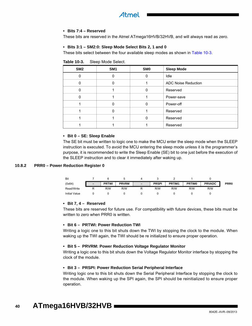
• Bits 7:4 – Reserved
These bits are reserved in the Atmel ATmega16HVB/32HVB, and will always read as zero.
• Bits 3:1 – SM2:0: Sleep Mode Select Bits 2, 1 and 0
These bits select between the four available sleep modes as shown in Table 10-3.
• Bit 0 – SE: Sleep Enable
The SE bit must be written to logic one to make the MCU enter the sleep mode when the SLEEPinstruction is executed. To avoid the MCU entering the sleep mode unless it is the programmer’spurpose, it is recommended to write the Sleep Enable (SE) bit to one just before the execution ofthe SLEEP instruction and to clear it immediately after waking up.
10.8.2 PRR0 – Power Reduction Register 0
• Bit 7, 4 – Reserved
These bits are reserved for future use. For compatibility with future devices, these bits must bewritten to zero when PRR0 is written.
• Bit 6 – PRTWI: Power Reduction TWI
Writing a logic one to this bit shuts down the TWI by stopping the clock to the module. Whenwaking up the TWI again, the TWI should be re initialized to ensure proper operation.
• Bit 5 – PRVRM: Power Reduction Voltage Regulator Monitor
Writing a logic one to this bit shuts down the Voltage Regulator Monitor interface by stopping theclock of the module.
• Bit 3 – PRSPI: Power Reduction Serial Peripheral Interface
Writing logic one to this bit shuts down the Serial Peripheral Interface by stopping the clock tothe module. When waking up the SPI again, the SPI should be reinitialized to ensure properoperation.
Table 10-3. Sleep Mode Select.
SM2 SM1 SM0 Sleep Mode
0 0 0 Idle
0 0 1 ADC Noise Reduction
0 1 0 Reserved
0 1 1 Power-save
1 0 0 Power-off
1 0 1 Reserved
1 1 0 Reserved
1 1 1 Reserved
Bit 7 6 5 4 3 2 1 0
(0x64) – PRTWI PRVRM – PRSPI PRTIM1 PRTIM0 PRVADC PRR0
Read/Write R R/W R/W R R/W R/W R/W R/W
Initial Value 0 0 0 0 0 0 0 0
408042E–AVR–09/2013
ATmega16HVB/32HVB
ATmega16HVB/32HVB
• Bit 2 – PRTIM1: Power Reduction Timer/Counter1
Writing a logic one to this bit shuts down the Timer/Counter1 module. When the Timer/Counter1is enabled, operation will continue like before the shutdown.
• Bit 1 – PRTIM0: Power Reduction Timer/Counter0
Writing a logic one to this bit shuts down the Timer/Counter0 module. When the Timer/Counter0is enabled, operation will continue like before the shutdown.
• Bit 0 – PRVADC: Power Reduction V-ADC
Writing a logic one to this bit shuts down the V-ADC. Before writing the PRVADC bit, make surethat the VADEN bit is cleared to minimize the power consumption.
Note: V-ADC control registers can be updated even if the PRVADC bit is set.
418042E–AVR–09/2013
11. System control and reset
11.1 Resetting the AVR
During reset, all I/O Registers are set to their initial values, and the program starts executionfrom the Reset Vector. The instruction placed at the Reset Vector must be a JMP – AbsoluteJump – instruction to the reset handling routine. If the program never enables an interruptsource, the Interrupt Vectors are not used, and regular program code can be placed at theselocations. The circuit diagram in ”Reset logic.” on page 43 shows the reset logic. Table 12-1 onpage 52 defines the electrical parameters of the reset circuitry.
The I/O ports of the AVR are immediately reset to their initial state when a reset source goesactive. This does not require any clock source to be running.
After all reset sources have gone inactive, a delay counter is invoked, stretching the internalreset. This allows the voltage regulator to reach a stable level before normal operation starts.The time-out period of the delay counter is defined by the user through the SUT Fuses. The dif-ferent selections for the delay period are presented in ”Clock sources” on page 26.
11.2 Reset sources
The Atmel ATmega16HVB/32HVB has five sources of reset:
• The Power-on Reset module generates a Power-on Reset when the Voltage Regulator starts up
• External Reset. The MCU is reset when a low level is present on the RESET pin for longer than the minimum pulse length
• Watchdog Reset. The MCU is reset when the Watchdog Timer period expires and the Watchdog is enabled
• Brown-out Reset. The MCU is reset when VREG is below the Brown-out Reset Threshold, VBOT. see ”Brown-out detection” on page 45
• debugWIRE Reset. In On-chip Debug mode, the debugWIRE resets the MCU when giving the Reset command
428042E–AVR–09/2013
ATmega16HVB/32HVB

ATmega16HVB/32HVB
Figure 11-1. Reset logic.
11.2.1 Power-on reset and charger connect
The Voltage Regulator will not start up until the Charger Detect module has enabled it. Beforethis happens the chip will be in Power-off mode and only the Charger Detect module is enabled.In order for the Charger Detect module to enable the Voltage Regulator, the voltage at the BATTpin must exceed the Power-On Threshold Voltage, VPOT. When the voltage at the BATT pinexceeds VPOT, the Voltage Regulator starts up and the chip enters RESET mode. When theDelay Counter times out, the chip will enter Active mode. See Figure 10-1 on page 36. Fordetails on Charger Detect, see ”Charger detect” on page 126.
MCU StatusRegister (MCUSR)
Reset Circuit
Delay Counters
CK
TIMEOUT
WD
RF
EX
TR
F
PO
RF
DATA BUS
ClockGenerator
SPIKEFILTER
Pull-up Resistor
BO
DR
F
Ultra Low PowerRC Oscillator
SUT[1:0]
Power-on ResetCircuit
WatchdogTimer
RESET/dW
POR
VREG
COUNTER RESET
Brown-outDetection
VCC
debugWIRE
OC
DR
F
438042E–AVR–09/2013
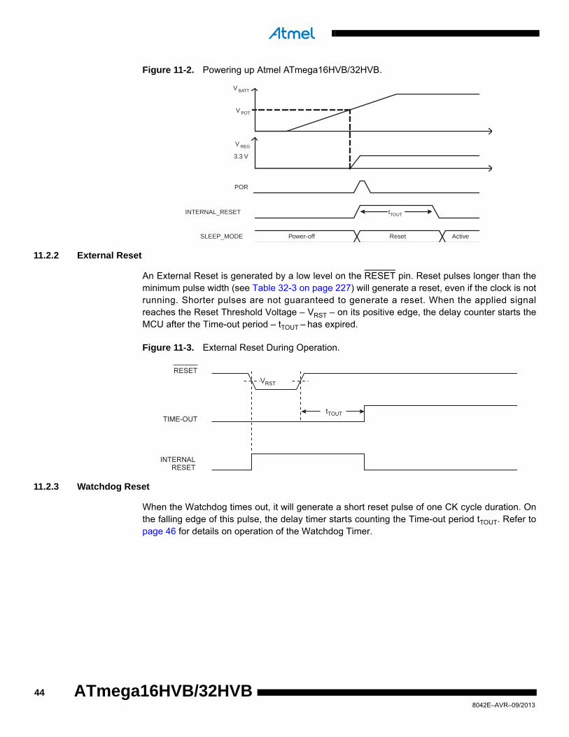
Figure 11-2. Powering up Atmel ATmega16HVB/32HVB.
11.2.2 External Reset
An External Reset is generated by a low level on the RESET pin. Reset pulses longer than theminimum pulse width (see Table 32-3 on page 227) will generate a reset, even if the clock is notrunning. Shorter pulses are not guaranteed to generate a reset. When the applied signalreaches the Reset Threshold Voltage – VRST – on its positive edge, the delay counter starts theMCU after the Time-out period – tTOUT – has expired.
Figure 11-3. External Reset During Operation.
11.2.3 Watchdog Reset
When the Watchdog times out, it will generate a short reset pulse of one CK cycle duration. Onthe falling edge of this pulse, the delay timer starts counting the Time-out period tTOUT. Refer topage 46 for details on operation of the Watchdog Timer.
Power-offSLEEP_MODE
POR
V BATT
INTERNAL_RESET tTOUT
Reset Active
V POT
V REG
3.3 V
448042E–AVR–09/2013
ATmega16HVB/32HVB
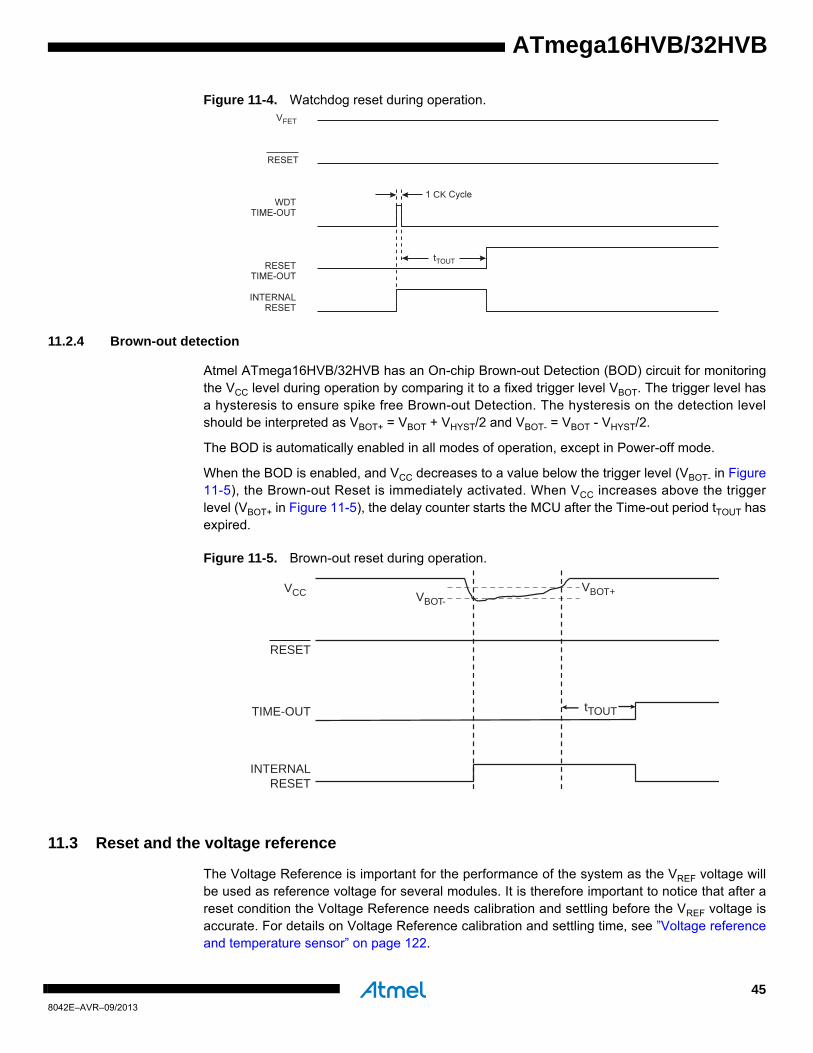
ATmega16HVB/32HVB
Figure 11-4. Watchdog reset during operation.
11.2.4 Brown-out detection
Atmel ATmega16HVB/32HVB has an On-chip Brown-out Detection (BOD) circuit for monitoringthe VCC level during operation by comparing it to a fixed trigger level VBOT. The trigger level hasa hysteresis to ensure spike free Brown-out Detection. The hysteresis on the detection levelshould be interpreted as VBOT+ = VBOT + VHYST/2 and VBOT- = VBOT - VHYST/2.
The BOD is automatically enabled in all modes of operation, except in Power-off mode.
When the BOD is enabled, and VCC decreases to a value below the trigger level (VBOT- in Figure11-5), the Brown-out Reset is immediately activated. When VCC increases above the triggerlevel (VBOT+ in Figure 11-5), the delay counter starts the MCU after the Time-out period tTOUT hasexpired.
Figure 11-5. Brown-out reset during operation.
11.3 Reset and the voltage reference
The Voltage Reference is important for the performance of the system as the VREF voltage willbe used as reference voltage for several modules. It is therefore important to notice that after areset condition the Voltage Reference needs calibration and settling before the VREF voltage isaccurate. For details on Voltage Reference calibration and settling time, see ”Voltage referenceand temperature sensor” on page 122.
CK
FET
VCC
RESET
TIME-OUT
INTERNALRESET
VBOT-VBOT+
tTOUT
458042E–AVR–09/2013
11.4 Watchdog timer
11.4.1 Features
• Clocked from separate nn-chip oscillator
• Three operating modes
– Interrupt
– System reset
– Interrupt and system reset
• Selectable time-out period from 16ms to 8s
• Possible hardware fuse watchdog always on (WDTON) for fail-safe mode
11.4.2 Overview
Atmel ATmega16HVB/32HVB has an Enhanced Watchdog Timer (WDT). The WDT countscycles of the Ultra Low Power RC Oscillator. The WDT gives an interrupt or a system reset whenthe counter reaches a given time-out value. In normal operation mode, it is required that the sys-tem uses the WDR - Watchdog Timer Reset - instruction to restart the counter before the time-out value is reached. If the system doesn't restart the counter, an interrupt or system reset willbe issued.
Figure 11-6. Watchdog timer.
In Interrupt mode, the WDT gives an interrupt when the timer expires. This interrupt can be usedto wake the device from sleep-modes, and also as a general system timer. One example is tolimit the maximum time allowed for certain operations, giving an interrupt when the operationhas run longer than expected. In System Reset mode, the WDT gives a reset when the timerexpires. This is typically used to prevent system hang-up in case of runaway code. The thirdmode, Interrupt and System Reset mode, combines the other two modes by first giving an inter-rupt and then switch to System Reset mode. This mode will for instance allow a safe shutdownby saving critical parameters before a system reset.
The Watchdog always on (WDTON) fuse, if programmed, will force the Watchdog Timer to Sys-tem Reset mode. With the fuse programmed the System Reset mode bit (WDE) and Interruptmode bit (WDIE) are locked to one and null respectively. To further ensure program security,alterations to the Watchdog set-up must follow timed sequences. The sequence for clearingWDE and changing time-out configuration is as follows:
Ultra Low Power RCOSCILLATOR
16 m
s 32
ms
64 m
s 0.
13s
0.26
s 0.
51s
1.0s
2.0s
4.
1s
8.2s
WDP0 WDP1WDP2WDP3
WATCHDOGRESET
WDE
WDIF
WDIE
MCU RESET
INTERRUPT
468042E–AVR–09/2013
ATmega16HVB/32HVB
ATmega16HVB/32HVB
1. In the same operation, write a logic one to the Watchdog change enable bit (WDCE) and WDE. A logic one must be written to WDE regardless of the previous value of the WDE bit.
2. Within the next four clock cycles, write the WDE and Watchdog prescaler bits (WDP) as desired, but with the WDCE bit cleared. This must be done in one operation.
The following code example shows one assembly and one C function for turning off the Watch-dog Timer. The example assumes that interrupts are controlled (for example by disablinginterrupts globally) so that no interrupts will occur during the execution of these functions.
Note: 1. See ”About code examples” on page 8.
Assembly code example (1)
WDT_off:
; Turn off global interrupt
cli
; Reset Watchdog Timer
wdr
; Clear WDRF in MCUSR
in r16, MCUSR
andi r16, (0xff & (0<<WDRF))
out MCUSR, r16
; Write logical one to WDCE and WDE
; Keep old prescaler setting to prevent unintentional time-out
in r16, WDTCSR
ori r16, (1<<WDCE) | (1<<WDE)
out WDTCSR, r16
; Turn off WDT
ldi r16, (0<<WDE)
out WDTCSR, r16
; Turn on global interrupt
sei
ret
C code example (1)
void WDT_off(void)
{
__disable_interrupt();
__watchdog_reset();
/* Clear WDRF in MCUSR */
MCUSR &= ~(1<<WDRF);
/* Write logical one to WDCE and WDE */
/* Keep old prescaler setting to prevent unintentional time-out */
WDTCSR |= (1<<WDCE) | (1<<WDE);
/* Turn off WDT */
WDTCSR = 0x00;
__enable_interrupt();
}
478042E–AVR–09/2013
Note: If the Watchdog is accidentally enabled, for example by a runaway pointer or brown-out condition, the device will be reset and the Watchdog Timer will stay enabled. If the code is not set up to han-dle the Watchdog, this might lead to an eternal loop of time-out resets. To avoid this situation, the application software should always clear the Watchdog System Reset Flag (WDRF) and the WDE control bit in the initialization routine, even if the Watchdog is not in use.
The following code example shows one assembly and one C function for changing the time-outvalue of the Watchdog Timer.
Note: 1. See ”About code examples” on page 8.
Note: The Watchdog Timer should be reset before any change of the WDP bits, since a changein the WDP bits can result in a time-out when switching to a shorter time-out period.
Assembly code example (1)
WDT_Prescaler_Change:
; Turn off global interrupt
cli
; Reset Watchdog Timer
wdr
; Start timed sequence
in r16, WDTCSR
ori r16, (1<<WDCE) | (1<<WDE)
out WDTCSR, r16
; -- Got four cycles to set the new values from here -
; Set new prescaler(time-out) value = 64K cycles (~0.5 s)
ldi r16, (1<<WDE) | (1<<WDP2) | (1<<WDP0)
out WDTCSR, r16
; -- Finished setting new values, used 2 cycles -
; Turn on global interrupt
sei
ret
C code example (1)
void WDT_Prescaler_Change(void)
{
__disable_interrupt();
__watchdog_reset();
/* Start timed equence */
WDTCSR |= (1<<WDCE) | (1<<WDE);
/* Set new prescaler(time-out) value = 64K cycles (~0.5 s) */
WDTCSR = (1<<WDE) | (1<<WDP2) | (1<<WDP0);
__enable_interrupt();
}
488042E–AVR–09/2013
ATmega16HVB/32HVB
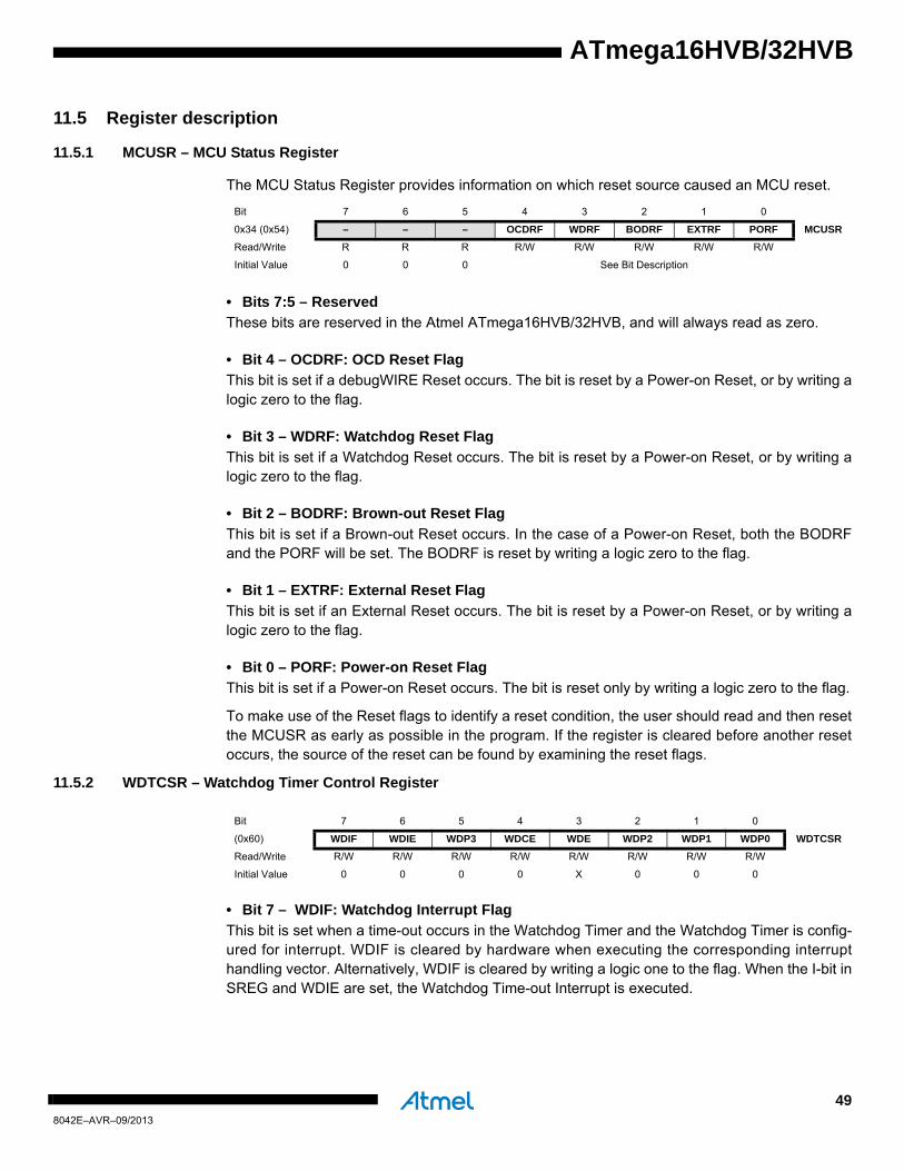
ATmega16HVB/32HVB
11.5 Register description
11.5.1 MCUSR – MCU Status Register
The MCU Status Register provides information on which reset source caused an MCU reset.
• Bits 7:5 – Reserved
These bits are reserved in the Atmel ATmega16HVB/32HVB, and will always read as zero.
• Bit 4 – OCDRF: OCD Reset Flag
This bit is set if a debugWIRE Reset occurs. The bit is reset by a Power-on Reset, or by writing alogic zero to the flag.
• Bit 3 – WDRF: Watchdog Reset Flag
This bit is set if a Watchdog Reset occurs. The bit is reset by a Power-on Reset, or by writing alogic zero to the flag.
• Bit 2 – BODRF: Brown-out Reset Flag
This bit is set if a Brown-out Reset occurs. In the case of a Power-on Reset, both the BODRFand the PORF will be set. The BODRF is reset by writing a logic zero to the flag.
• Bit 1 – EXTRF: External Reset Flag
This bit is set if an External Reset occurs. The bit is reset by a Power-on Reset, or by writing alogic zero to the flag.
• Bit 0 – PORF: Power-on Reset Flag
This bit is set if a Power-on Reset occurs. The bit is reset only by writing a logic zero to the flag.
To make use of the Reset flags to identify a reset condition, the user should read and then resetthe MCUSR as early as possible in the program. If the register is cleared before another resetoccurs, the source of the reset can be found by examining the reset flags.
11.5.2 WDTCSR – Watchdog Timer Control Register
• Bit 7 – WDIF: Watchdog Interrupt Flag
This bit is set when a time-out occurs in the Watchdog Timer and the Watchdog Timer is config-ured for interrupt. WDIF is cleared by hardware when executing the corresponding interrupthandling vector. Alternatively, WDIF is cleared by writing a logic one to the flag. When the I-bit inSREG and WDIE are set, the Watchdog Time-out Interrupt is executed.
Bit 7 6 5 4 3 2 1 0
0x34 (0x54) – – – OCDRF WDRF BODRF EXTRF PORF MCUSR
Read/Write R R R R/W R/W R/W R/W R/W
Initial Value 0 0 0 See Bit Description
Bit 7 6 5 4 3 2 1 0
(0x60) WDIF WDIE WDP3 WDCE WDE WDP2 WDP1 WDP0 WDTCSR
Read/Write R/W R/W R/W R/W R/W R/W R/W R/W
Initial Value 0 0 0 0 X 0 0 0
498042E–AVR–09/2013

• Bit 6 – WDIE: Watchdog Interrupt Enable
When this bit is written to one and the I-bit in the Status Register is set, the Watchdog Interrupt isenabled. If WDE is cleared in combination with this setting, the Watchdog Timer is in InterruptMode, and the corresponding interrupt is executed if time-out in the Watchdog Timer occurs.
If WDE is set, the Watchdog Timer is in Interrupt and System Reset Mode. The first time-out inthe Watchdog Timer will set WDIF. Executing the corresponding interrupt vector will clear WDIEand WDIF automatically by hardware (the Watchdog goes to System Reset Mode). This is use-ful for keeping the Watchdog Timer security while using the interrupt. To stay in Interrupt andSystem Reset Mode, WDIE must be set after each interrupt. This should however not be donewithin the interrupt service routine itself, as this might compromise the safety-function of theWatchdog System Reset mode. If the interrupt is not executed before the next time-out, a Sys-tem Reset will be applied.
Note: 1. WDTON fuse set to “0” means programmed, “1” means unprogrammed.
• Bit 5, 2:0 – WDP3:0 : Watchdog Timer Prescaler three, two, one, and null
The WDP3..0 bits determine the Watchdog Timer prescaling when the Watchdog Timer isenabled. The different prescaling values and their corresponding Timeout Periods are shown inTable 11-2 on page 51.
• Bit 4 – WDCE: Watchdog Change Enable
This bit is used in timed sequences for changing WDE and prescaler bits. To clear the WDE bit,and/or change the prescaler bits, WDCE must be set.
Once written to one, hardware will clear WDCE after four clock cycles.
• Bit 3 – WDE: Watchdog System Reset Enable
WDE is overridden by WDRF in MCUSR. This means that WDE is always set when WDRF isset. To clear WDE, WDRF must be cleared first. This feature ensures multiple resets during con-ditions causing failure, and a safe start-up after the failure.
• Bits 5, 2:0 – WDP3:0: Watchdog Timer Prescaler three, two, one, and null
The WDP3..0 bits determine the Watchdog Timer prescaling when the Watchdog Timer isenabled. The different prescaling values and their corresponding Timeout Periods are shown inTable 11-2 on page 51.
Table 11-1. Watchdog timer configuration.
WDTON (1) WDE WDIE Mode Action on timeout
1 0 0 Stopped None
1 0 1 Interrupt mode Interrupt
1 1 0 System Reset mode Reset
1 1 1Interrupt and System Reset mode
Interrupt, then go to System Reset mode
0 x x System Reset mode Reset
508042E–AVR–09/2013
ATmega16HVB/32HVB
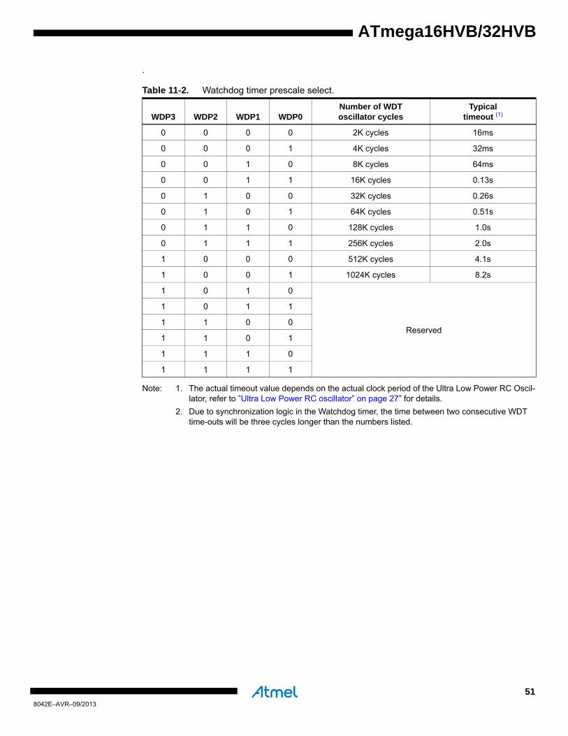
ATmega16HVB/32HVB
.
Note: 1. The actual timeout value depends on the actual clock period of the Ultra Low Power RC Oscil-lator, refer to ”Ultra Low Power RC oscillator” on page 27” for details.
2. Due to synchronization logic in the Watchdog timer, the time between two consecutive WDT time-outs will be three cycles longer than the numbers listed.
Table 11-2. Watchdog timer prescale select.
WDP3 WDP2 WDP1 WDP0Number of WDToscillator cycles
Typicaltimeout (1)
0 0 0 0 2K cycles 16ms
0 0 0 1 4K cycles 32ms
0 0 1 0 8K cycles 64ms
0 0 1 1 16K cycles 0.13s
0 1 0 0 32K cycles 0.26s
0 1 0 1 64K cycles 0.51s
0 1 1 0 128K cycles 1.0s
0 1 1 1 256K cycles 2.0s
1 0 0 0 512K cycles 4.1s
1 0 0 1 1024K cycles 8.2s
1 0 1 0
Reserved
1 0 1 1
1 1 0 0
1 1 0 1
1 1 1 0
1 1 1 1
518042E–AVR–09/2013

12. Interrupts
12.1 Overview
This section describes the specifics of the interrupt handling as performed in AtmelATmega16HVB/32HVB. For a general explanation of the AVR interrupt handling, refer to ”Resetand interrupt handling” on page 14.
12.2 Interrupt vectors in Atmel ATmega16HVB/32HVB
Table 12-1. Reset and interrupt vectors.
VectorNo.
Programaddress (1) Source Interrupt definition
1 0x0000 RESETExternal pin, power-on reset, brown-out reset, watchdog reset, and debugWIRE reset
2 0x0002 BPINT Battery protection interrupt
3 0x0004 VREGMON Voltage regulator monitor interrupt
4 0x0006 INT0 External Interrupt Request 0
5 0x0008 INT1 External Interrupt Request 1
6 0x000A INT2 External Interrupt Request 2
7 0x000C INT3 External Interrupt Request 3
8 0x000E PCINT0 Pin Change Interrupt 0
9 0x0010 PCINT1 Pin Change Interrupt 1
10 0x0012 WDT Watchdog timeout interrupt
11 0x0014 BGSCD Bandgap buffer short circuit detected
12 0x0016 CHDET Charger detect
13 0x0018 TIMER1 IC Timer/Counter 1 input capture
14 0x001A TIMER1 COMPA Timer/Counter 1 compare Match A
15 0x001C TIMER1 COMPB Timer/Counter 1 compare Match B
16 0x001E TIMER1 OVF Timer/Counter 1 overflow
17 0x0020 TIMER0 IC Timer/Counter 0 input capture
18 0x0022 TIMER0 COMPA Timer/Counter 0 compare Match A
19 0x0024 TIMER0 COMPB Timer /Counter0 compare Match B
20 0x0026 TIMER0 OVF Timer/Counter 0 overflow
21 0x0028 TWI BUS C/D Two-wire bus connect/disconnect
22 0x002A TWI Two-wire serial interface
23 0x002C SPI, STC SPI, Serial Transfer Complete
24 0x002E VADC Voltage ADC conversion complete
25 0x0030 CCADC CONV CC-ADC instantaneous current conversion complete
26 0x0032 CCADC REG CUR CC-ADC regular current
528042E–AVR–09/2013
ATmega16HVB/32HVB
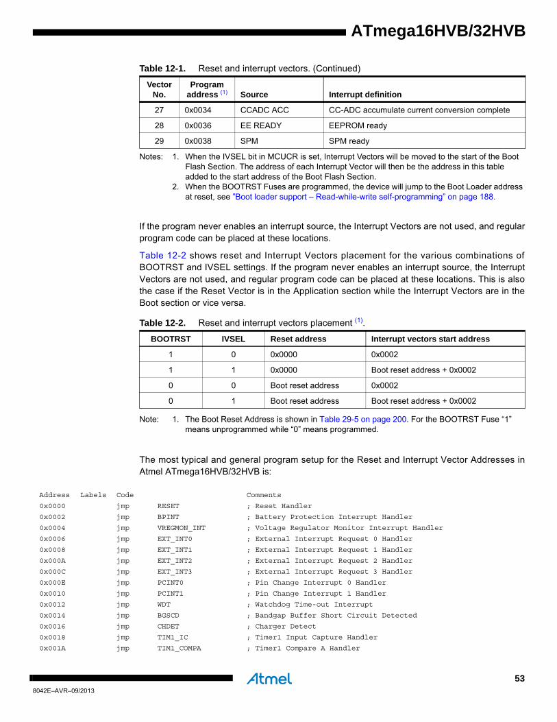
ATmega16HVB/32HVB
Notes: 1. When the IVSEL bit in MCUCR is set, Interrupt Vectors will be moved to the start of the Boot Flash Section. The address of each Interrupt Vector will then be the address in this table added to the start address of the Boot Flash Section.
2. When the BOOTRST Fuses are programmed, the device will jump to the Boot Loader address at reset, see ”Boot loader support – Read-while-write self-programming” on page 188.
If the program never enables an interrupt source, the Interrupt Vectors are not used, and regularprogram code can be placed at these locations.
Table 12-2 shows reset and Interrupt Vectors placement for the various combinations ofBOOTRST and IVSEL settings. If the program never enables an interrupt source, the InterruptVectors are not used, and regular program code can be placed at these locations. This is alsothe case if the Reset Vector is in the Application section while the Interrupt Vectors are in theBoot section or vice versa.
Note: 1. The Boot Reset Address is shown in Table 29-5 on page 200. For the BOOTRST Fuse “1” means unprogrammed while “0” means programmed.
The most typical and general program setup for the Reset and Interrupt Vector Addresses inAtmel ATmega16HVB/32HVB is:
27 0x0034 CCADC ACC CC-ADC accumulate current conversion complete
28 0x0036 EE READY EEPROM ready
29 0x0038 SPM SPM ready
Table 12-2. Reset and interrupt vectors placement (1).
BOOTRST IVSEL Reset address Interrupt vectors start address
1 0 0x0000 0x0002
1 1 0x0000 Boot reset address + 0x0002
0 0 Boot reset address 0x0002
0 1 Boot reset address Boot reset address + 0x0002
Table 12-1. Reset and interrupt vectors. (Continued)
VectorNo.
Programaddress (1) Source Interrupt definition
Address Labels Code Comments
0x0000 jmp RESET ; Reset Handler
0x0002 jmp BPINT ; Battery Protection Interrupt Handler
0x0004 jmp VREGMON_INT ; Voltage Regulator Monitor Interrupt Handler
0x0006 jmp EXT_INT0 ; External Interrupt Request 0 Handler
0x0008 jmp EXT_INT1 ; External Interrupt Request 1 Handler
0x000A jmp EXT_INT2 ; External Interrupt Request 2 Handler
0x000C jmp EXT_INT3 ; External Interrupt Request 3 Handler
0x000E jmp PCINT0 ; Pin Change Interrupt 0 Handler
0x0010 jmp PCINT1 ; Pin Change Interrupt 1 Handler
0x0012 jmp WDT ; Watchdog Time-out Interrupt
0x0014 jmp BGSCD ; Bandgap Buffer Short Circuit Detected
0x0016 jmp CHDET ; Charger Detect
0x0018 jmp TIM1_IC ; Timer1 Input Capture Handler
0x001A jmp TIM1_COMPA ; Timer1 Compare A Handler
538042E–AVR–09/2013

When the BOOTRST Fuse is unprogrammed, the Boot section size set to 4Kbytes and the IVSEL bit in the MCUCR Regis-ter is set before any interrupts are enabled, the most typical and general program setup for the Reset and Interrupt VectorAddresses is:
Address Labels Code Comments
0x0000 RESET: ldi r16,high(RAMEND); Main program start
0x0001 out SPH,r16 ; Set Stack Pointer to top of RAM
0x0002 ldi r16,low(RAMEND)
0x0003 out SPL,r160x0004 sei ; Enable interrupts
0x0005 <instr> xxx
;
.org 0x4C02
0x4C02 jmp BPINT ; Battery Protection Interrupt Handler
0x4C04 jmp EXT_INT0 ; External Interrupt Request 0 Handler
... ... ... ;
0x4C2C jmp SPM_RDY ; Store Program Memory Ready Handler
When the BOOTRST Fuse is programmed and the Boot section size set to 4Kbytes, the most typical and general programsetup for the Reset and Interrupt Vector Addresses is:
Address Labels Code Comments
.org 0x0002
0x0002 jmp BPINT ; Battery Protection Interrupt Handler
0x0004 jmp EXT_INT0 ; External Interrupt Request 0 Handler
0x001C jmp TIM1_COMPB ; Timer1 Compare B Handler
0x001E jmp TIM1_OVF ; Timer1 Overflow Handler
0X0020 jmp TIM0_IC ; Timer0 Input Capture Handler
0x0022 jmp TIM0_COMPA ; Timer0 CompareA Handler
0x0024 jmp TIM0_COMPB ; Timer0 CompareB Handler
0x0026 jmp TIM0_OVF ; Timer0 Overflow Handler
0x0028 jmp TWI_BUS_CD ; Two-wire Bus Connect/Disconnect Handler
0x002A jmp TWI ; Two-wire Serial Interface Handler
0x002C jmp SPI, STC ; SPI, Serial Transfer Complete
0x002E jmp VADC ; Voltage ADC Conversion Complete Handler
0x0030 jmp CCADC_CONV ; CC-ADC Instantaneous Current Conversion Complete Handler
0x0032 jmp CCADC_REC_CUR ; CC-ADC Regular Current Handler
0x0034 jmp CCADC_ACC ; CC-ADC Accumulate Current Conversion Complete Handler
0x0036 jmp EE_RDY ; EEPROM Ready Handler
0x0038 jmp SPM ; Store Program Memory Ready Handler
;
0x003A RESET: ldi r16, high(RAMEND) ; Main program start
0x003B out SPH,r16 ; Set Stack Pointer to top of RAM
0x003C ldi r16, low(RAMEND)
0x003D out SPL,r16
0x003E sei ; Enable interrupts
0x003F <instr> xxx
0x0040 ... ... ...
;
548042E–AVR–09/2013
ATmega16HVB/32HVB

ATmega16HVB/32HVB
... ... ... ;
0x002C jmp SPM_RDY ; Store Program Memory Ready Handler
;
.org 0x4C000x4C00 RESET: ldi r16,high(RAMEND); Main program start
0x4C01 out SPH,r16 ; Set Stack Pointer to top of RAM
0x4C02 ldi r16,low(RAMEND)
0x4C03 out SPL,r160x4C04 sei ; Enable interrupts
0x4C05 <instr> xxx
When the BOOTRST Fuse is programmed, the Boot section size set to 4Kbytes and the IVSEL bit in the MCUCR Registeris set before any interrupts are enabled, the most typical and general program setup for the Reset and Interrupt VectorAddresses is:
Address Labels Code Comments
;
.org 0x4C000x4C00 jmp RESET ; Reset handler0x4C02 jmp BPINT ; Battery Protection Interrupt Handler
0x4C04 jmp EXT_INT0 ; External Interrupt Request 0 Handler
... ... ... ;
0x4C2C jmp SPM_RDY ; Store Program Memory Ready Handler
;
0x4C2E RESET: ldi r16,high(RAMEND); Main program start
0x4C2F out SPH,r16 ; Set Stack Pointer to top of RAM
0x4C30 ldi r16,low(RAMEND)
0x4C31 out SPL,r160x4C32 sei ; Enable interrupts
0x4C33 <instr> xxx
558042E–AVR–09/2013

12.3 Moving interrupts between application and boot spaceThe General Interrupt Control Register controls the placement of the Interrupt Vector table.
12.4 Register description
12.4.1 MCUCR – MCU Control Register
• Bit 1 – IVSEL: Interrupt Vector Select
When the IVSEL bit is cleared (zero), the Interrupt Vectors are placed at the start of the Flashmemory. When this bit is set (one), the Interrupt Vectors are moved to the beginning of the BootLoader section of the Flash. The actual address of the start of the Boot Flash Section is deter-mined by the BOOTSZ Fuses. Refer to the section ”Boot loader support – Read-while-write self-programming” on page 188 for details. To avoid unintentional changes of Interrupt Vector tables,a special write procedure must be followed to change the IVSEL bit:
a. Write the Interrupt Vector Change Enable (IVCE) bit to one.
b. Within four cycles, write the desired value to IVSEL while writing a zero to IVCE.
Interrupts will automatically be disabled while this sequence is executed. Interrupts are disabledin the cycle IVCE is set, and they remain disabled until after the instruction following the write toIVSEL. If IVSEL is not written, interrupts remain disabled for four cycles. The I-bit in the StatusRegister is unaffected by the automatic disabling.
Note: If Interrupt Vectors are placed in the Boot Loader section and Boot Lock bit BLB02 is pro-grammed, interrupts are disabled while executing from the Application section. If Interrupt Vectors are placed in the Application section and Boot Lock bit BLB12 is programed, interrupts are dis-
Assembly code example
Move_interrupts:
; Enable change of Interrupt Vectors
ldi r16, (1<<IVCE)
out MCUCR, r16
; Move interrupts to Boot Flash section
ldi r16, (1<<IVSEL)
out MCUCR, r16
ret
C code example
void Move_interrupts(void)
{
/* Enable change of Interrupt Vectors */
MCUCR = (1<<IVCE);
/* Move interrupts to Boot Flash section */
MCUCR = (1<<IVSEL);
}
Bit 7 6 5 4 3 2 1 0
0x35 (0x55) JTD – – PUD – – IVSEL IVCE MCUCR
Read/Write R/W R R R/W R R R/W R/W
Initial Value 0 0 0 0 0 0 0 0
568042E–AVR–09/2013
ATmega16HVB/32HVB

ATmega16HVB/32HVB
abled while executing from the Boot Loader section. Refer to the section ”Boot loader support – Read-while-write self-programming” on page 188 for details on Boot Lock bits.
• Bit 0 – IVCE: Interrupt Vector Change Enable
The IVCE bit must be written to logic one to enable change of the IVSEL bit. IVCE is cleared byhardware four cycles after it is written or when IVSEL is written. Setting the IVCE bit will disableinterrupts, as explained in the IVSEL description above. See Code Example in ”Moving inter-rupts between application and boot space” on page 56.
578042E–AVR–09/2013

13. External interrupts
13.1 Overview
The External Interrupts are triggered by the INT3:0 pin or any of the PCINT11:0 pins. Observethat, if enabled, the interrupts will trigger even if the INT3:0 or PCINT11:0 pins are configured asoutputs. This feature provides a way of generating a software interrupt.
The External Interrupts can be triggered by a falling or rising edge or a low level. This is set upas indicated in the specification for the “EICRA – External Interrupt Control Register A” . Whenthe external interrupt is enabled and is configured as level triggered, the interrupt will trigger aslong as the pin is held low. Interrupts are detected asynchronously. This implies that these inter-rupts can be used for waking the part also from sleep modes other than Idle mode. The I/O clockis halted in all sleep modes except Idle mode.
The Pin change interrupt PCI1 will trigger if any enabled PCINT11:4 pin toggles and Pin changeinterrupts PCI0 will trigger if any enabled PCINT3:0 pin toggles. PCMSK1 and PCMSK0 Regis-ters control which pins contribute to the pin change interrupts. Pin change interrupts onPCINT11:0 are detected asynchronously. This implies that these interrupts can be used for wak-ing the part also from sleep modes other than Idle mode.
Note that if a level triggered interrupt is used for wake-up from Power-save, the required levelmust be held long enough for the MCU to complete the wake-up to trigger the level interrupt. Ifthe level disappears before the end of the Start-up Time, the MCU will still wake up, but no inter-rupt will be generated. The start-up time is defined by the SUT fuses as described in ”Clocksystems and their distribution” on page 25.
13.2 Register description
13.2.1 EICRA – External Interrupt Control Register A
• Bits 7:0 – ISCn: External Interrupt Sense Control Bits
The External Interrupts 3:0 are activated by the external pins INT3:0 if the SREG I-flag and thecorresponding interrupt mask in the EIMSK is set. The level and edges on the external pins thatactivate the interrupts are defined in Table 13-1 on page 59. Edges on INT3..INT0 are registeredasynchronously. Pulses on INT3:0 pins wider than the minimum pulse width given in Table 32-11 on page 230 will generate an interrupt. Shorter pulses are not guaranteed to generate aninterrupt. If low level interrupt is selected, the low level must be held until the completion of thecurrently executing instruction to generate an interrupt. If enabled, a level triggered interrupt willgenerate an interrupt request as long as the pin is held low. When changing the ISCn bit, aninterrupt can occur. Therefore, it is recommended to first disable INTn by clearing its InterruptEnable bit in the EIMSK Register. Then, the ISCn bit can be changed. Finally, the INTn interruptflag should be cleared by writing a logical one to its Interrupt Flag bit (INTFn) in the EIFR Regis-ter before the interrupt is re-enabled.
Bit 7 6 5 4 3 2 1 0
(0x69) ISC31 ISC30 ISC21 ISC20 ISC11 ISC10 ISC01 ISC00 EICRA
Read/Write R/W R/W R/W R/W R/W R/W R/W R/W
Initial Value 0 0 0 0 0 0 0 0
588042E–AVR–09/2013
ATmega16HVB/32HVB

ATmega16HVB/32HVB
Note: 1. n = 3, 2, 1, or 0.When changing the ISCn1/ISCn0 bits, the interrupt must be disabled by clearing its InterruptEnable bit in the EIMSK Register. Otherwise an interrupt can occur when the bits are changed.
13.2.2 EIMSK – External Interrupt Mask Register
• Bits 7:4 – Reserved
These bits are reserved ins the Atmel ATmega16HVB/32HVB, and will always read as zero.
• Bits 3:0 – INT3 – INT0: External Interrupt Request 3:0 enable
When an INT3 – INT0 bit is written to one and the I-bit in the Status Register (SREG) is set(one), the corresponding external pin interrupt is enabled. The Interrupt Sense Control bits in theExternal Interrupt Control Register – EICRA – defines whether the external interrupt is activatedon rising or falling edge or level sensed. Activity on any of these pins will trigger an interruptrequest even if the pin is enabled as an output. This provides a way of generating a softwareinterrupt.
13.2.3 EIFR – External Interrupt Flag Register
• Bits 7:4 – Reserved
These bits are reserved ins the ATmega16HVB/32HVB, and will always read as zero.
• Bits 3:0 – INTF3 – INTF0: External Interrupt Flags 3:0
When an edge or logic change on the INT3:0 pin triggers an interrupt request, INTF3:0 becomesset (one). If the I-bit in SREG and the corresponding interrupt enable bit, INT3:0 in EIMSK, areset (one), the MCU will jump to the interrupt vector. The flag is cleared when the interrupt routineis executed. Alternatively, the flag can be cleared by writing a logical one to it. These flags arealways cleared when INT3:0 are configured as level interrupt. Note that when entering sleepmode with the INT3:0 interrupts disabled, the input buffers on these pins will be disabled. Thismay cause a logic change in internal signals which will set the INTF3:0 flags. See ”Digital inputenable and sleep modes” on page 71 for more information.
Table 13-1. Interrupt sense control.
ISCn1 ISCn0 Description
0 0 The low level of INTn generates an interrupt request
0 1 Any logical change on INTn generates an interrupt request
1 0 The falling edge of INTn generates an interrupt request
1 1 The rising edge of INTn generates an interrupt request
Bit 7 6 5 4 3 2 1 0
0x1D (0x3D) – – – – INT3 INT2 INT1 INT0 EIMSK
Read/Write R R R R R/W R/W R/W R/W
Initial Value 0 0 0 0 0 0 0 0
Bit 7 6 5 4 3 2 1 0
0x1C (0x3C) – – – – INTF3 INTF2 INTF1 INTF0 EIFR
Read/Write R R R R R/W R/W R/W R/W
Initial Value 0 0 0 0 0 0 0 0
598042E–AVR–09/2013
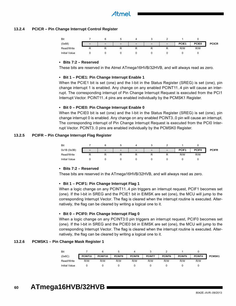
13.2.4 PCICR – Pin Change Interrupt Control Register
• Bits 7:2 – Reserved
These bits are reserved in the Atmel ATmega16HVB/32HVB, and will always read as zero.
• Bit 1 – PCIE1: Pin Change Interrupt Enable 1
When the PCIE1 bit is set (one) and the I-bit in the Status Register (SREG) is set (one), pinchange interrupt 1 is enabled. Any change on any enabled PCINT11..4 pin will cause an inter-rupt. The corresponding interrupt of Pin Change Interrupt Request is executed from the PCI1Interrupt Vector. PCINT11..4 pins are enabled individually by the PCMSK1 Register.
• Bit 0 – PCIE0: Pin Change Interrupt Enable 0
When the PCIE0 bit is set (one) and the I-bit in the Status Register (SREG) is set (one), pinchange interrupt 0 is enabled. Any change on any enabled PCINT3..0 pin will cause an interrupt.The corresponding interrupt of Pin Change Interrupt Request is executed from the PCI0 Inter-rupt Vector. PCINT3..0 pins are enabled individually by the PCMSK0 Register.
13.2.5 PCIFR – Pin Change Interrupt Flag Register
• Bits 7:2 – Reserved
These bits are reserved in the ATmega16HVB/32HVB, and will always read as zero.
• Bit 1 – PCIF1: Pin Change Interrupt Flag 1
When a logic change on any PCINT11..4 pin triggers an interrupt request, PCIF1 becomes set(one). If the I-bit in SREG and the PCIE1 bit in EIMSK are set (one), the MCU will jump to thecorresponding Interrupt Vector. The flag is cleared when the interrupt routine is executed. Alter-natively, the flag can be cleared by writing a logical one to it.
• Bit 0 – PCIF0: Pin Change Interrupt Flag 0
When a logic change on any PCINT3:0 pin triggers an interrupt request, PCIF0 becomes set(one). If the I-bit in SREG and the PCIE0 bit in EIMSK are set (one), the MCU will jump to thecorresponding Interrupt Vector. The flag is cleared when the interrupt routine is executed. Alter-natively, the flag can be cleared by writing a logical one to it.
13.2.6 PCMSK1 – Pin Change Mask Register 1
Bit 7 6 5 4 3 2 1 0
(0x68) – – – – – – PCIE1 PCIE0 PCICR
Read/Write R R R R R R R/W R/W
Initial Value 0 0 0 0 0 0 0 0
Bit 7 6 5 4 3 2 1 0
0x1B (0x3B) – – – – – – PCIF1 PCIF0 PCIFR
Read/Write R R R R R R R/W R/W
Initial Value 0 0 0 0 0 0 0 0
Bit 7 6 5 4 3 2 1 0
(0x6C) PCINT11 PCINT10 PCINT9 PCINT8 PCINT7 PCINT6 PCINT5 PCINT4 PCMSK1
Read/Write R/W R/W R/W R/W R/W R/W R/W R/W
Initial Value 0 0 0 0 0 0 0 0
608042E–AVR–09/2013
ATmega16HVB/32HVB
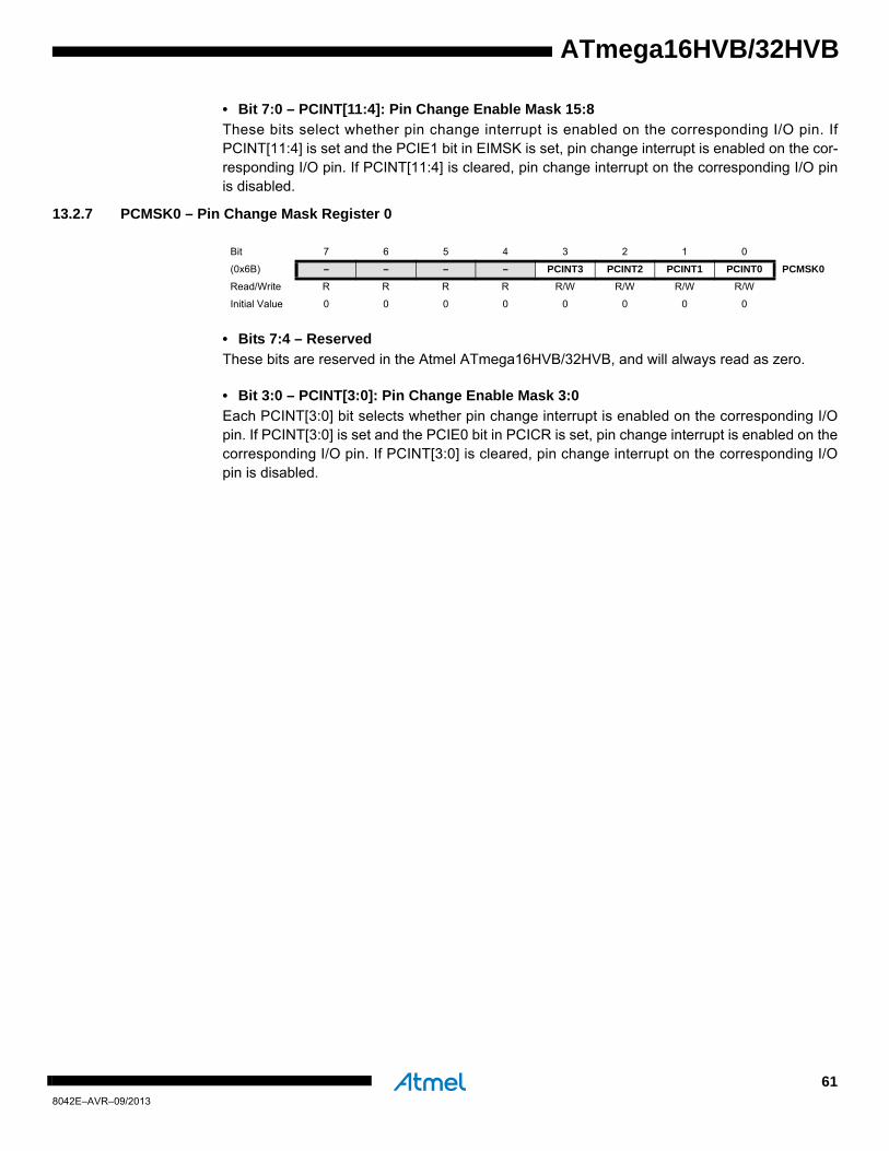
ATmega16HVB/32HVB
• Bit 7:0 – PCINT[11:4]: Pin Change Enable Mask 15:8
These bits select whether pin change interrupt is enabled on the corresponding I/O pin. IfPCINT[11:4] is set and the PCIE1 bit in EIMSK is set, pin change interrupt is enabled on the cor-responding I/O pin. If PCINT[11:4] is cleared, pin change interrupt on the corresponding I/O pinis disabled.
13.2.7 PCMSK0 – Pin Change Mask Register 0
• Bits 7:4 – Reserved
These bits are reserved in the Atmel ATmega16HVB/32HVB, and will always read as zero.
• Bit 3:0 – PCINT[3:0]: Pin Change Enable Mask 3:0
Each PCINT[3:0] bit selects whether pin change interrupt is enabled on the corresponding I/Opin. If PCINT[3:0] is set and the PCIE0 bit in PCICR is set, pin change interrupt is enabled on thecorresponding I/O pin. If PCINT[3:0] is cleared, pin change interrupt on the corresponding I/Opin is disabled.
Bit 7 6 5 4 3 2 1 0
(0x6B) – – – – PCINT3 PCINT2 PCINT1 PCINT0 PCMSK0
Read/Write R R R R R/W R/W R/W R/W
Initial Value 0 0 0 0 0 0 0 0
618042E–AVR–09/2013

14. High voltage I/O ports
14.1 Overview
All high voltage AVR ports have true Read-Modify-Write functionality when used as general dig-ital I/O ports. This means that the state of one port pin can be changed without unintentionallychanging the state of any other pin with the SBI and CBI instructions. All high voltage I/O pinshave protection Zener diodes to Ground as indicated in Figure 14-1. See ”Electrical characteris-tics” on page 225 for a complete list of parameters.
Figure 14-1. High voltage I/O pin equivalent schematic.
All registers and bit references in this section are written in general form. A lower case “x” repre-sents the numbering letter for the port, and a lower case “n” represents the bit number. However,when using the register or bit defines in a program, the precise form must be used. For example,PORTC3 for bit number three in Port C, here documented generally as PORTxn. The physicalI/O Registers and bit locations are listed in ”Register description” on page 66.
One I/O Memory address location is allocated for each high voltage port, the Data Register –PORTx. The Data Register is read/write.
Using the I/O port as General Digital Output is described in ”High voltage ports as general digitalI/O” on page 63.
Cpin
Logic
See Figure"General High Voltage Digital I/O" for Details
Pxn
628042E–AVR–09/2013
ATmega16HVB/32HVB

ATmega16HVB/32HVB
14.2 High voltage ports as general digital I/O
The high voltage ports are high voltage tolerant open collector output ports. In addition they canbe used as general digital inputs. Figure 14-2 shows a functional description of one output portpin, here generically called Pxn.
Figure 14-2. General high voltage digital I/O (1).
Notes: 1. WRx, RRx and RPx are common to all pins within the same port. clkI/O and SLEEP are com-mon to all ports.
2. The High Voltage Digital Input is not present on PC5.14.2.1 Configuring the pin
Each port pin consist of two register bits: PORTxn and PINxn. As shown in ”Register description”on page 66, the PORTxn bits are accesed at the PORTx I/O address, and the PINxn bits at thePINx I/O address.
If PORTxn is written logic one, the port pin is driven low (zero). If PORTxn is written logic zero,the port pin is tri-stated. The port pins are tri-stated when a reset condition becomes active, evenif no clocks are running.
14.2.2 Reading the pin
The port pin can be read through the PINxn Register bit. As shown in Figure 14-2, the PINxnRegister bit and the preceding latch constitute a synchronizer. This is needed to avoid metasta-bility if the physical pin changes value near the edge of the internal clock, but it also introduces adelay.
WRx
SLEEP: SLEEP CONTROLclkI/O: I/O CLOCK
SLEEP
Pxn
Q D
Q
PORTxn_
CLR
DAT
AB
US
RRx
SYNCHRONIZER
QD
CLR
PINxn
clkI/O
Q_
D
L
Q
Q
SET
CLR
_
RESET
RPx
RRx: READ PORTx REGISTERWRx: WRITE PORTx REGISTERRPx: READ PINx REGISTER
HIGH VOLTAGE DIGITAL INPUT(2)
638042E–AVR–09/2013

14.3 Overview
14.4 Alternate port functions
The High Voltage I/O has alternate port functions in addition to being general digital I/O. Figure14-3 shows how the port pin control signals from the simplified Figure 14-2 on page 63 can beoverridden by alternate functions.
Figure 14-3. High voltage digital I/O (1)(2).
Notes: 1. WRx, RRx and RPx are common to all pins within the same port. clkI/O and SLEEP are com-mon to all ports. All other signals are unique for each pin.
2. The High Voltage Digital Input is not present on PC5.
Table 14-1 on page 65 summarizes the function of the overriding signals. The pin and portindexes from Figure 14-3 are not shown in the succeeding tables. The overriding signals aregenerated internally in the modules having the alternate function.
WRx
PVOVxn
PVOExn
PVOExn: Pxn PORT VALUE OVERRIDE ENABLEPVOVxn: Pxn PORT VALUE OVERRIDE VALUEDIEOExn: Pxn DIGITAL INPUT-ENABLE OVERRIDE ENABLEDIEOVxn: Pxn DIGITAL INPUT-ENABLE OVERRIDE VALUE
SLEEP
Pxn
DIEOExn
DIEOVxn
Q D
Q
PORTxn_
CLR
1
0
1
0
DAT
AB
USRRx
SYNCHRONIZER
QD
CLR
PINxn
clkI/O
Q_
D
L
Q
Q
SET
CLR
_
RESET
RPx
DIxn
RRx: READ PORTx REGISTERWRx: WRITE PORTx REGISTERRPx: READ PINx REGISTERclkI/O: I/O CLOCKDIxn: DIGITAL INPUT PIN n ON PORTxSLEEP: SLEEP CONTROL
648042E–AVR–09/2013
ATmega16HVB/32HVB

ATmega16HVB/32HVB
14.4.1 Alternate functions of Port C
The Port C pins with alternate functions are shown in Table 14-2.
The alternate pin configuration is as follows:
• INT0/ EXTPROT – Port C, Bit0
INT0: External Interrupt Source 0. This pin can serve as external interrupt source. INT0 can beused as an interrupt pin regardless of whether another function is enabled or not.
EXTPROT: External Battery Protection Input. This pin can serve as external battery protectioninput to be able to override the FET controller externally.
• INT1 – Port C, Bit1
INT1: External Interrupt Source 1. This pin can serve as external interrupt source. INT1 can beused as an interrupt pin regardless of whether another function is enabled or not.
• INT2 – Port C, Bit2
INT2: External Interrupt Source 2. This pin can serve as external interrupt source. INT2 can beused as an interrupt pin regardless of whether another function is enabled or not.
Table 14-1. Generic description of overriding signals for alternate functions.
Signal name Full name Description
PVOEPort value override enable
If this signal is set and the Output Driver is enabled, the port value is controlled by the PVOV signal. If PVOE is cleared, and the Output Driver is enabled, the port Value is controlled by the PORTxn Register bit
PVOVPort value override value
If PVOE is set, the port value is set to PVOV, regardless of the setting of the PORTxn Register bit
DIEOEDigital input enable override enable
If this bit is set, the Digital Input Enable is controlled by the DIEOV signal. If this signal is cleared, the Digital Input Enable is determined by MCU state (Normal mode, sleep mode)
DIEOVDigital input enable override value
If DIEOE is set, the Digital Input is enabled/disabled when DIEOV is set/cleared, regardless of the MCU state (Normal mode, sleep mode)
DI Digital input
This is the Digital Input to alternate functions. In the figure, the signal is connected to the output of the schmitt trigger but before the synchronizer. Unless the Digital Input is used as a clock source, the module with the alternate function will use its own synchronizer
Table 14-2. Port C pins alternate functions.
Port pin Alternate function
PC0 INT0/ EXTPROT(External Interrupt 0 or External Battery Protection Input)
PC1 INT1 (External Interrupt 1)
PC2 INT1 (External Interrupt 2)
PC3 INT3/ SDA (External Interrupt 3 or SM bus data line)
PC4 SCL (SM Bus Clock line)
658042E–AVR–09/2013
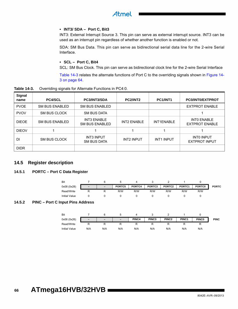
• INT3/ SDA – Port C, Bit3
INT3: External Interrupt Source 3. This pin can serve as external interrupt source. INT3 can beused as an interrupt pin regardless of whether another function is enabled or not.
SDA: SM Bus Data. This pin can serve as bidirectional serial data line for the 2-wire SerialInterface.
• SCL – Port C, Bit4
SCL: SM Bus Clock. This pin can serve as bidirectional clock line for the 2-wire Serial Interface
Table 14-3 relates the alternate functions of Port C to the overriding signals shown in Figure 14-3 on page 64.
14.5 Register description
14.5.1 PORTC – Port C Data Register
14.5.2 PINC – Port C Input Pins Address
Table 14-3. Overriding signals for Alternate Functions in PC4:0.
Signalname PC4/SCL PC3/INT3/SDA PC2/INT2 PC1/INT1 PC0/INT0/EXTPROT
PVOE SM BUS ENABLED SM BUS ENABLED EXTPROT ENABLE
PVOV SM BUS CLOCK SM BUS DATA 1
DIEOE SM BUS ENABLEDINT3 ENABLE
SM BUS ENABLEDINT2 ENABLE INT1ENABLE
INT0 ENABLEEXTPROT ENABLE
DIEOV 1 1 1 1 1
DI SM BUS CLOCKINT3 INPUT
SM BUS DATAINT2 INPUT INT1 INPUT
INT0 INPUTEXTPROT INPUT
DIDR
Bit 7 6 5 4 3 2 1 0
0x08 (0x28) – – PORTC5 PORTC4 PORTC3 PORTC2 PORTC1 PORTC0 PORTC
Read/Write R R R/W R/W R/W R/W R/W R/W
Initial Value 0 0 0 0 0 0 0 0
Bit 7 6 5 4 3 2 1 0
0x06 (0x26) – – – PINC4 PINC3 PINC2 PINC1 PINC0 PINC
Read/Write R R R R R R R R
Initial Value N/A N/A N/A N/A N/A N/A N/A N/A
668042E–AVR–09/2013
ATmega16HVB/32HVB

ATmega16HVB/32HVB
15. Low voltage I/O-Ports
15.1 Overview
All low voltage AVR ports have true Read-Modify-Write functionality when used as general digi-tal I/O ports. This means that the direction of one port pin can be changed without unintentionallychanging the direction of any other pin with the SBI and CBI instructions. The same applieswhen changing drive value (if configured as output) or enabling/disabling of pull-up resistors (ifconfigured as input). All low voltage port pins have individually selectable pull-up resistors with asupply-voltage invariant resistance. All I/O pins have protection diodes to both VREG and Groundas indicated in Figure 15-1. Refer to ”Electrical characteristics” on page 225 for a complete list ofparameters.
Figure 15-1. Low voltage I/O pin equivalent schematic.
All registers and bit references in this section are written in general form. A lower case “x” repre-sents the numbering letter for the port, and a lower case “n” represents the bit number. However,when using the register or bit defines in a program, the precise form must be used. For example,PORTB3 for bit no. 3 in Port B, here documented generally as PORTxn. The physical I/O Regis-ters and bit locations are listed in ”Register description” on page 78.
Three I/O memory address locations are allocated for each low voltage port, one each for theData Register – PORTx, Data Direction Register – DDRx, and the Port Input Pins – PINx. ThePort Input Pins I/O location is read only, while the Data Register and the Data Direction Registerare read/write. However, writing a logic one to a bit in the PINx Register, will result in a toggle inthe corresponding bit in the Data Register. In addition, the Pull-up Disable – PUD bit in MCUCRdisables the pull-up function for all low voltage pins in all ports when set.
Using the I/O port as General Digital I/O is described in ”Low voltage ports as general digital I/O”on page 68. Many low voltage port pins are multiplexed with alternate functions for the periph-eral features on the device. How each alternate function interferes with the port pin is describedin ”Alternate port functions” on page 72. Refer to the individual module sections for a full descrip-tion of the alternate functions.
Note that enabling the alternate function of some of the port pins does not affect the use of theother pins in the port as general digital I/O.
Cpin
Logic
Rpu
See Figure"General Digital I/O" for
Details
Pxn
678042E–AVR–09/2013

15.2 Low voltage ports as general digital I/O
The low voltage ports are bi-directional I/O ports with optional internal pull-ups. Figure 15-2shows a functional description of one I/O-port pin, here generically called Pxn.
Figure 15-2. General low voltage digital I/O (1).
Note: 1. WRx, WPx, WDx, RRx, RPx, and RDx are common to all pins within the same port. clkI/O, SLEEP, and PUD are common to all ports.
15.2.1 Configuring the pin
Each port pin consists of three register bits: DDxn, PORTxn, and PINxn. As shown in ”Registerdescription” on page 78, the DDxn bits are accessed at the DDRx I/O address, the PORTxn bitsat the PORTx I/O address, and the PINxn bits at the PINx I/O address.
The DDxn bit in the DDRx Register selects the direction of this pin. If DDxn is written logic one,Pxn is configured as an output pin. If DDxn is written logic zero, Pxn is configured as an inputpin.
If PORTxn is written logic one when the pin is configured as an input pin, the pull-up resistor isactivated. To switch the pull-up resistor off, PORTxn has to be written logic zero or the pin has tobe configured as an output pin. The port pins are tri-stated when reset condition becomes active,even if no clocks are running.
If PORTxn is written logic one when the pin is configured as an output pin, the port pin is drivenhigh (one). If PORTxn is written logic zero when the pin is configured as an output pin, the portpin is driven low (zero).
clk
RPx
RRx
RDx
WDx
PUD
SYNCHRONIZER
WDx: WRITE DDRx
WRx: WRITE PORTxRRx: READ PORTx REGISTERRPx: READ PORTx PIN
PUD: PULLUP DISABLE
clkI/O: I/O CLOCK
RDx: READ DDRx
D
L
Q
Q
RESET
RESET
Q
QD
Q
Q D
CLR
PORTxn
Q
Q D
CLR
DDxn
PINxn
DAT
A B
US
SLEEP
SLEEP: SLEEP CONTROL
Pxn
I/O
WPx
0
1
WRx
WPx: WRITE PINx REGISTER
688042E–AVR–09/2013
ATmega16HVB/32HVB

ATmega16HVB/32HVB
15.2.2 Toggling the pin
Writing a logic one to PINxn toggles the value of PORTxn, independent on the value of DDRxn.Note that the SBI instruction can be used to toggle one single bit in a port.
15.2.3 Switching between input and output
When switching between tri-state ({DDxn, PORTxn} = 0b00) and output high ({DDxn, PORTxn}= 0b11), an intermediate state with either pull-up enabled {DDxn, PORTxn} = 0b01) or outputlow ({DDxn, PORTxn} = 0b10) must occur. Normally, the pull-up enabled state is fully accept-able, as a high-impedant environment will not notice the difference between a strong high driverand a pull-up. If this is not the case, the PUD bit in the MCUCR Register can be set to disable allpull-ups in all ports.
Switching between input with pull-up and output low generates the same problem. The usermust use either the tri-state ({DDxn, PORTxn} = 0b00) or the output high state ({DDxn, PORTxn}= 0b11) as an intermediate step.
Table 15-1 summarizes the control signals for the pin value.
15.2.4 Reading the pin value
Independent of the setting of Data Direction bit DDxn, the port pin can be read through thePINxn Register bit. As shown in Figure 15-2 on page 68, the PINxn Register bit and the preced-ing latch constitute a synchronizer. This is needed to avoid metastability if the physical pinchanges value near the edge of the internal clock, but it also introduces a delay. Figure 15-3 onpage 70 shows a timing diagram of the synchronization when reading an externally applied pinvalue. The maximum and minimum propagation delays are denoted tpd,max and tpd,min
respectively.
Table 15-1. Port pin configurations.
DDxn PORTxnPUD
(in MCUCR) I/O Pull-up Comment
0 0 X Input No Tri-state (Hi-Z)
0 1 0 Input Yes Pxn will source current if ext. pulled low
0 1 1 Input No Tri-state (Hi-Z)
1 0 X Output No Output Low (Sink)
1 1 X Output No Output High (Source)
698042E–AVR–09/2013
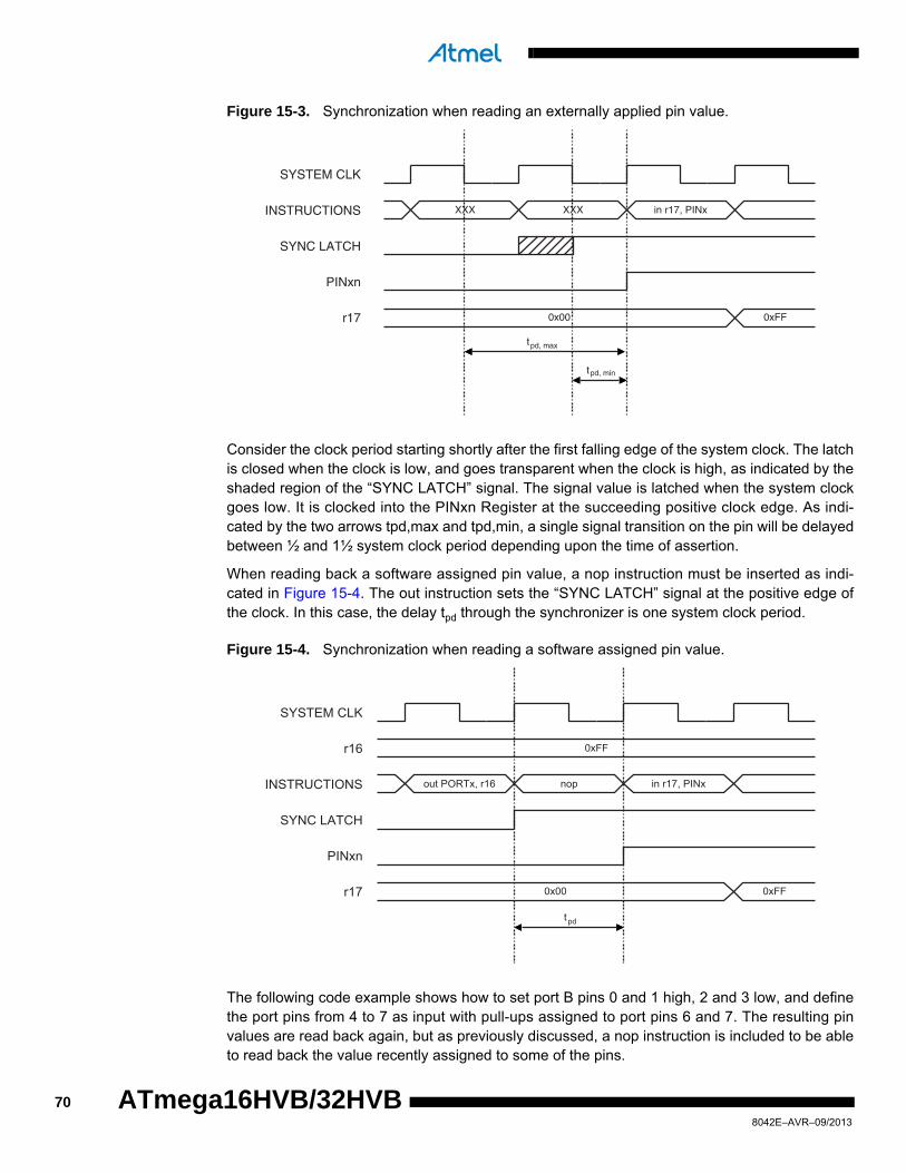
Figure 15-3. Synchronization when reading an externally applied pin value.
Consider the clock period starting shortly after the first falling edge of the system clock. The latchis closed when the clock is low, and goes transparent when the clock is high, as indicated by theshaded region of the “SYNC LATCH” signal. The signal value is latched when the system clockgoes low. It is clocked into the PINxn Register at the succeeding positive clock edge. As indi-cated by the two arrows tpd,max and tpd,min, a single signal transition on the pin will be delayedbetween ½ and 1½ system clock period depending upon the time of assertion.
When reading back a software assigned pin value, a nop instruction must be inserted as indi-cated in Figure 15-4. The out instruction sets the “SYNC LATCH” signal at the positive edge ofthe clock. In this case, the delay tpd through the synchronizer is one system clock period.
Figure 15-4. Synchronization when reading a software assigned pin value.
The following code example shows how to set port B pins 0 and 1 high, 2 and 3 low, and definethe port pins from 4 to 7 as input with pull-ups assigned to port pins 6 and 7. The resulting pinvalues are read back again, but as previously discussed, a nop instruction is included to be ableto read back the value recently assigned to some of the pins.
XXX in r17, PINx
0x00 0xFF
INSTRUCTIONS
SYNC LATCH
PINxn
r17
XXX
SYSTEM CLK
tpd, max
tpd, min
out PORTx, r16 nop in r17, PINx
0xFF
0x00 0xFF
SYSTEM CLK
r16
INSTRUCTIONS
SYNC LATCH
PINxn
r17
tpd
708042E–AVR–09/2013
ATmega16HVB/32HVB

ATmega16HVB/32HVB
Note: 1. For the assembly program, two temporary registers are used to minimize the time from pull-ups are set on pins 0, 1, 6, and 7, until the direction bits are correctly set, defining bit 2 and 3 as low and redefining bits 0 and 1 as strong high drivers.
15.2.5 Digital input enable and sleep modes
As shown in Figure 15-2 on page 68, the digital input signal can be clamped to ground at theinput of the schmiSchmidtt-trigger. The signal denoted SLEEP in the figure, is set by the MCUSleep Controller in Power-save mode to avoid high power consumption if some input signals areleft floating, or have an analog signal level close to VREG/2.
SLEEP is overridden for port pins enabled as external interrupt pins. If the external interruptrequest is not enabled, SLEEP is active also for these pins. SLEEP is also overridden by variousother alternate functions as described in ”Alternate port functions” on page 72.
If a logic high level (“one”) is present on an asynchronous external interrupt pin configured as“Interrupt on Rising Edge, Falling Edge, or Any Logic Change on Pin” while the external interruptis not enabled, the corresponding External Interrupt Flag will be set when resuming from theabove mentioned Sleep mode, as the clamping in these sleep mode produces the requestedlogic change.
Assembly code example (1)
...
; Define pull-ups and set outputs high
; Define directions for port pins
ldi r16,(1<<PB7)|(1<<PB6)|(1<<PB1)|(1<<PB0)
ldi r17,(1<<DDB3)|(1<<DDB2)|(1<<DDB1)|(1<<DDB0)
out PORTB,r16
out DDRB,r17
; Insert nop for synchronization
nop
; Read port pins
in r16,PINB
...
C code example
unsigned char i;
...
/* Define pull-ups and set outputs high */
/* Define directions for port pins */
PORTB = (1<<PB7)|(1<<PB6)|(1<<PB1)|(1<<PB0);
DDRB = (1<<DDB3)|(1<<DDB2)|(1<<DDB1)|(1<<DDB0);
/* Insert nop for synchronization*/
_NOP();
/* Read port pins */
i = PINB;
...
718042E–AVR–09/2013

15.2.6 Unconnected pins
If some pins are unused, it is recommended to ensure that these pins have a defined level. Eventhough most of the digital inputs are disabled in the deep sleep modes as described above, float-ing inputs should be avoided to reduce current consumption in all other modes where the digitalinputs are enabled (Reset, Active mode and Idle mode).
The simplest method to ensure a defined level of an unused pin, is to enable the internal pull-up.In this case, the pull-up will be disabled during reset. If low power consumption during reset isimportant, it is recommended to use an external pull-up or pull-down. Connecting unused pinsdirectly to VCC or GND is not recommended, since this may cause excessive currents if the pin isaccidentally configured as an output.
15.3 Alternate port functions
Many low voltage port pins have alternate functions in addition to being general digital I/Os. Fig-ure 15-5 shows how the port pin control signals from the simplified Figure 15-2 on page 68 canbe overridden by alternate functions. The overriding signals may not be present in all port pins,but the figure serves as a generic description applicable to all port pins in the AVR microcon-troller family.
Figure 15-5. Alternate port functions (1).
Note: 1. WRx, WPx, WDx, RRx, RPx, and RDx are common to all pins within the same port. clkI/O, SLEEP, and PUD are common to all ports. All other signals are unique for each pin.
clk
RPx
RRxWRx
RDx
WDx
PUD
SYNCHRONIZER
WDx: WRITE DDRx
WRx: WRITE PORTxRRx: READ PORTx REGISTER
RPx: READ PORTx PIN
PUD: PULLUP DISABLE
clkI/O: I/O CLOCK
RDx: READ DDRx
D
L
Q
Q
SET
CLR
0
1
0
1
0
1
DIxn
AIOxn
DIEOExn
PVOVxn
PVOExn
DDOVxn
DDOExn
PUOExn
PUOVxn
PUOExn: Pxn PULL-UP OVERRIDE ENABLEPUOVxn: Pxn PULL-UP OVERRIDE VALUEDDOExn: Pxn DATA DIRECTION OVERRIDE ENABLEDDOVxn: Pxn DATA DIRECTION OVERRIDE VALUEPVOExn: Pxn PORT VALUE OVERRIDE ENABLEPVOVxn: Pxn PORT VALUE OVERRIDE VALUE
DIxn: DIGITAL INPUT PIN n ON PORTxAIOxn: ANALOG INPUT/OUTPUT PIN n ON PORTx
RESET
RESET
Q
Q D
CLR
Q
Q D
CLR
Q
QD
CLR
PINxn
PORTxn
DDxn
DAT
A B
US
0
1DIEOVxn
SLEEP
DIEOExn: Pxn DIGITAL INPUT-ENABLE OVERRIDE ENABLEDIEOVxn: Pxn DIGITAL INPUT-ENABLE OVERRIDE VALUESLEEP: SLEEP CONTROL
Pxn
I/O
0
1
PTOExn
WPx
PTOExn: Pxn, PORT TOGGLE OVERRIDE ENABLE
WPx: WRITE PINx
728042E–AVR–09/2013
ATmega16HVB/32HVB
ATmega16HVB/32HVB
Table 15-2 summarizes the function of the overriding signals. The pin and port indexes from Fig-ure 15-5 on page 72 are not shown in the succeeding tables. The overriding signals aregenerated internally in the modules having the alternate function.
The following subsections shortly describe the alternate functions for each port, and relate theoverriding signals to the alternate function. Refer to the alternate function description for furtherdetails.
Table 15-2. Generic description of overriding signals for alternate functions.
Signal name Full name Description
PUOEPull-up override enable
If this signal is set, the pull-up enable is controlled by the PUOV signal. If this signal is cleared, the pull-up is enabled when {DDxn, PORTxn, PUD} = 0b010
PUOVPull-up override value
If PUOE is set, the pull-up is enabled/disabled when PUOV is set/cleared, regardless of the setting of the DDxn, PORTxn, and PUD Register bits
DDOEData direction override enable
If this signal is set, the Output Driver Enable is controlled by the DDOV signal. If this signal is cleared, the Output driver is enabled by the DDxn Register bit
DDOVData direction override value
If DDOE is set, the Output Driver is enabled/disabled when DDOV is set/cleared, regardless of the setting of the DDxn Register bit
PVOEPort value override enable
If this signal is set and the Output Driver is enabled, the port value is controlled by the PVOV signal. If PVOE is cleared, and the Output Driver is enabled, the port Value is controlled by the PORTxn Register bit
PVOVPort value override value
If PVOE is set, the port value is set to PVOV, regardless of the setting of the PORTxn Register bit
PTOEPort toggle override enable
If PTOE is set, the PORTxn Register bit is inverted
DIEOEDigital input enable override enable
If this bit is set, the Digital Input Enable is controlled by the DIEOV signal. If this signal is cleared, the Digital Input Enable is determined by MCU state (Normal mode, sleep mode)
DIEOVDigital input enable override value
If DIEOE is set, the Digital Input is enabled/disabled when DIEOV is set/cleared, regardless of the MCU state (Normal mode, sleep mode)
DI Digital input
This is the Digital Input to alternate functions. In the figure, the signal is connected to the output of the schmitt trigger but before the synchronizer. Unless the Digital Input is used as a clock source, the module with the alternate function will use its own synchronizer
AIOAnalog input/output
This is the Analog Input/output to/from alternate functions. The signal is connected directly to the pad, and can be used bi-directionally
738042E–AVR–09/2013

15.3.1 Alternate functions of Port A
The Port A pins with alternate functions are shown in Table 15-3.
The alternate pin configuration is as follows:
• ADC0/SGND/PCINT0 – Port A, Bit0
ADC0: Voltage ADC Channel0. This pin can serve as Channel 0 Input for the Voltage ADC.
SGND: Voltage ADC Signal Ground. This pin can serve as Channel 1 Signal Ground for theVoltage ADC.
PCINT0. Pin Change Interrupt 0. This pin can serve as external interrupt source.
• ADC1/SGND/PCINT1 – Port A, Bit1
ADC1: Voltage ADC Channel 1: This pin can serve as Channel 1 for the Voltage ADC.
SGND: Voltage ADC Signal Ground. This pin can serve as Channel 0 Signal Ground for theVoltage ADC.
PCINT1: Pin Change Interrupt 1. This pin can serve as external interrupt source.
• T0/PCINT2 – Port A, Bit2
T0: Timer/Counter0. This pin can serve as Timer/Counter0 clock source.
PCINT2: Pin Change Interrupt 2. This pin can serve as external interrupt source.
• T1/PCINT3 – Port A, Bit3
T1: Timer/Counter1. This pin can serve as Timer/Counter1 clock source.
PCINT3: Pin Change Interrupt 3.
These pins can serve as external interrupt source. Table 15-4 on page 75 relates the alternatefunctions of Port A to the overriding signals shown in Figure 15-5 on page 72.
Table 15-3. Port A pins alternate functions.
Port pin Alternate function
PA3 T1/PCINT3 (Timer/Counter1 Clock Input or Pin Change Interrupt 3)
PA2 T0/PCINT2 (Timer/Counter0 Clock Input or Pin Change Interrupt 2)
PA1ADC1/SGND/PCINT1(ADC Input Channel 1, Signal Ground or Pin Change Interrupt 1)
PA0ADC0/SGND/PCINT0(ADC Input Channel 0, Signal Ground or Pin Change Interrupt 0)
748042E–AVR–09/2013
ATmega16HVB/32HVB
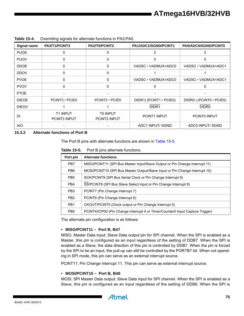
ATmega16HVB/32HVB
15.3.2 Alternate functions of Port B
The Port B pins with alternate functions are shown in Table 15-5.
The alternate pin configuration is as follows:
• MISO/PCINT11 – Port B, Bit7
MISO, Master Data input: Slave Data output pin for SPI channel. When the SPI is enabled as aMaster, this pin is configured as an input regardless of the setting of DDB7. When the SPI isenabled as a Slave, the data direction of this pin is controlled by DDB7. When the pin is forcedby the SPI to be an input, the pull-up can still be controlled by the PORTB7 bit. When not operat-ing in SPI mode, this pin can serve as an external interrupt source.
PCINT11: Pin Change Interrupt 11. This pin can serve as external interrupt source.
• MOSI/PCINT10 – Port B, Bit6
MOSI, SPI Master Data output: Slave Data input for SPI channel. When the SPI is enabled as aSlave, this pin is configured as an input regardless of the setting of DDB6. When the SPI is
Table 15-4. Overriding signals for alternate functions in PA3:PA0.
Signal name PA3/T1/PCINT3 PA2/T0/PCINT2 PA1/ADC1/SGND/PCINT1 PA0/ADC0/SGND/PCINT0
PUOE 0 0 0 0
PUOV 0 0 0 0
DDOE 0 0 VADSC • VADMUX=ADC0 VADSC • VADMUX=ADC1
DDOV 0 0 1 1
PVOE 0 0 VADSC • VADMUX=ADC0 VADSC • VADMUX=ADC1
PVOV 0 0 0 0
PTOE - - - -
DIEOE PCINT3 • PCIE0 PCINT2 • PCIE0 DIDR1| (PCINT1 • PCIE0) DIDR0 | (PCINT0 • PCIE0)
DIEOV 1 1 DIDR1 DIDR0
DIT1 INPUT
PCINT3 INPUT
T0 INPUT
PCINT2 INPUTPCINT1 INPUT PCINT0 INPUT
AIO - - ADC1 INPUT/ SGND ADC0 INPUT/ SGND
Table 15-5. Port B pins alternate functions.
Port pin Alternate functions
PB7 MISO/PCINT11 (SPI Bus Master Input/Slave Output or Pin Change Interrupt 11)
PB6 MOSI/PCINT10 (SPI Bus Master Output/Slave Input or Pin Change Interrupt 10)
PB5 SCK/PCINT9 (SPI Bus Serial Clock or Pin Change Interrupt 9)
PB4 SS/PCINT8 (SPI Bus Slave Select input or Pin Change Interrupt 8)
PB3 PCINT7 (Pin Change Interrupt 7)
PB2 PCINT6 (Pin Change Interrupt 6)
PB1 CKOUT/PCINT5 (Clock output or Pin Change Interrupt 5)
PB0 PCINT4/ICP00 (Pin Change Interrupt 4 or Timer/Counter0 Input Capture Trigger)
758042E–AVR–09/2013
enabled as a Master, the data direction of this pin is controlled by DDB6. When the pin is forcedby the SPI to be an input, the pull-up can still be controlled by the PORTB6 bit. When not operat-ing in SPI mode, this pin can serve as an external interrupt source.
PCINT10: Pin Change Interrupt 10. This pin can serve as external interrupt source.
• SCK/PCINT9 – Port B, Bit5
SCK, Master Clock output: Slave Clock input pin for SPI channel. When the SPI is enabled as aSlave, this pin is configured as an input regardless of the setting of DDB5. When the SPI isenabled as a Master, the data direction of this pin is controlled by DDB5. When the pin is forcedby the SPI to be an input, the pull-up can still be controlled by the PORTB5 bit.
PCINT9: Pin Change Interrupt 9. This pin can serve as external interrupt source.
• SS/PCINT8 – Port B, Bit4
SS, Slave Select input: When the SPI is enabled as a Slave, this pin is configured as an inputregardless of the setting of DDB4. As a Slave, the SPI is activated when this pin is driven low.When the SPI is enabled as a Master, the data direction of this pin is controlled by DDB4. Whenthe pin is forced by the SPI to be an input, the pull-up can still be controlled by the PORTB4 bit.When not operating in SPI mode, this pin can serve as Clock Output, CPU Clock divided by 2.See ”Clock output” on page 28.
PCINT8: Pin Change Interrupt 8. This pin can serve as external interrupt source.
• PCINT7 – Port B, Bit3
PCINT7: Pin Change Interrupt 7. This pin can serve as external interrupt source.
• PCINT6 – Port B, Bit2
PCINT6: Pin Change Interrupt 6. This pin can serve as external interrupt source.
• CKOUT/PCINT5 – Port B, Bit1
CKOUT: Clock output. This pin can serve as clock output pin.
PCINT5: Pin Change Interrupt 5. This pin can serve as external interrupt source.
• ICP00/PCINT4 – Port B, Bit0
ICP00: Input Capture Timer/Counter0. This pin can serve as Input Capture Trigger forTimer/Counter0.
PCINT4: Pin Change Interrupt 4. This pin can serve as external interrupt source.
768042E–AVR–09/2013
ATmega16HVB/32HVB
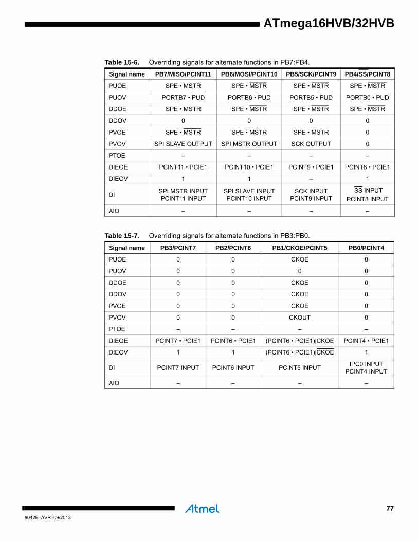
ATmega16HVB/32HVB
Table 15-6. Overriding signals for alternate functions in PB7:PB4.
Signal name PB7/MISO/PCINT11 PB6/MOSI/PCINT10 PB5/SCK/PCINT9 PB4/SS/PCINT8
PUOE SPE • MSTR SPE • MSTR SPE • MSTR SPE • MSTR
PUOV PORTB7 • PUD PORTB6 • PUD PORTB5 • PUD PORTB0 • PUD
DDOE SPE • MSTR SPE • MSTR SPE • MSTR SPE • MSTR
DDOV 0 0 0 0
PVOE SPE • MSTR SPE • MSTR SPE • MSTR 0
PVOV SPI SLAVE OUTPUT SPI MSTR OUTPUT SCK OUTPUT 0
PTOE – – – –
DIEOE PCINT11 • PCIE1 PCINT10 • PCIE1 PCINT9 • PCIE1 PCINT8 • PCIE1
DIEOV 1 1 – 1
DISPI MSTR INPUTPCINT11 INPUT
SPI SLAVE INPUTPCINT10 INPUT
SCK INPUTPCINT9 INPUT
SS INPUT
PCINT8 INPUT
AIO – – – –
Table 15-7. Overriding signals for alternate functions in PB3:PB0.
Signal name PB3/PCINT7 PB2/PCINT6 PB1/CKOE/PCINT5 PB0/PCINT4
PUOE 0 0 CKOE 0
PUOV 0 0 0 0
DDOE 0 0 CKOE 0
DDOV 0 0 CKOE 0
PVOE 0 0 CKOE 0
PVOV 0 0 CKOUT 0
PTOE – – – –
DIEOE PCINT7 • PCIE1 PCINT6 • PCIE1 (PCINT6 • PCIE1)|CKOE PCINT4 • PCIE1
DIEOV 1 1 (PCINT6 • PCIE1)|CKOE 1
DI PCINT7 INPUT PCINT6 INPUT PCINT5 INPUTIPC0 INPUT
PCINT4 INPUT
AIO – – – –
778042E–AVR–09/2013

15.4 Register description
15.4.1 MCUCR – MCU Control Register
• Bit 4 – PUD: Pull-up disable
When this bit is written to one, the pull-ups in the I/O ports are disabled even if the DDxn andPORTxn Registers are configured to enable the pull-ups ({DDxn, PORTxn} = 0b01). See ”Con-figuring the pin” on page 68 for more details about this feature.
15.4.2 PORTA – Port A Data Register
15.4.3 DDRA – Port A Data Direction Register
15.4.4 PINA – Port A Input Pins Address
15.4.5 PORTB – Port B Data Register
15.4.6 DDRB – Port B Data Direction Register
15.4.7 PINB – Port B Input Pins Address
Bit 7 6 5 4 3 2 1 0
0x35 (0x55) – – CKOE PUD – – IVSEL IVCE MCUCR
Read/Write R R R/W R/W R R R/W R/W
Initial Value 0 0 0 0 0 0 0 0
Bit 7 6 5 4 3 2 1 0
0x02 (0x22) – – – – PORTA3 PORTA2 PORTA1 PORTA0 PORTA
Read/Write R R R R R/W R/W R/W R/W
Initial Value 0 0 0 0 0 0 0 0
Bit 7 6 5 4 3 2 1 0
0x01 (0x21) – – – – DDA3 DDA2 DDA1 DDA0 DDRA
Read/Write R R R R R/W R/W R/W R/W
Initial Value 0 0 0 0 0 0 0 0
Bit 7 6 5 4 3 2 1 0
0x00 (0x20) – – – – PINA3 PINA2 PINA1 PINA0 PINA
Read/Write R R R R R/W R/W R/W R/W
Initial Value N/A N/A N/A N/A N/A N/A N/A N/A
Bit 7 6 5 4 3 2 1 0
0x05 (0x25) PORTB7 PORTB6 PORTB5 PORTB4 PORTB3 PORTB2 PORTB1 PORTB0 PORTB
Read/Write R/W R/W R/W R/W R/W R/W R/W R/W
Initial Value 0 0 0 0 0 0 0 0
Bit 7 6 5 4 3 2 1 0
0x04 (0x24) DDB7 DDB6 DDB5 DDB4 DDB3 DDB2 DDB1 DDB0 DDRB
Read/Write R/W R/W R/W R/W R/W R/W R/W R/W
Initial Value 0 0 0 0 0 0 0 0
Bit 7 6 5 4 3 2 1 0
0x03 (0x23) PINB7 PINB6 PINB5 PINB4 PINB3 PINB2 PINB1 PINB0 PINB
Read/Write R R R R R R R R
Initial Value N/A N/A N/A N/A N/A N/A N/A N/A
788042E–AVR–09/2013
ATmega16HVB/32HVB

ATmega16HVB/32HVB
16. Timer/Counter0 and Timer/Counter1 prescalers
16.1 Overview
Timer/Counter1 and Timer/Counter0 share the same prescaler module, but the Timer/Counterscan have different prescaler settings. The description below applies to both Timer/Counter1 andTimer/Counter0.
16.1.1 Internal clock source
The Timer/Counter can be clocked directly by the system clock (by setting the CSn2:0 = 1). Thisprovides the fastest operation, with a maximum Timer/Counter clock frequency equal to systemclock frequency (fCLK_I/O). Alternatively, one of four taps from the prescaler can be used as aclock source. The prescaled clock has a frequency of either fCLK_I/O/8, fCLK_I/O/64, fCLK_I/O/256, orfCLK_I/O/1024.
16.1.2 Prescaler reset
The prescaler is free running, that is, operates independently of the Clock Select logic of theTimer/Counter, and it is shared by Timer/Counter1 and Timer/Counter0. Since the prescaler isnot affected by the Timer/Counter’s clock select, the state of the prescaler will have implicationsfor situations where a prescaled clock is used. One example of prescaling artifacts occurs whenthe timer is enabled and clocked by the prescaler (6 > CSn2:0 > 1). The number of system clockcycles from when the timer is enabled to the first count occurs can be from 1 to N+1 systemclock cycles, where N equals the prescaler divisor (8, 64, 256, or 1024).
It is possible to use the prescaler reset for synchronizing the Timer/Counter to program execu-tion. However, care must be taken if the other Timer/Counter that shares the same prescaleralso uses prescaling. A prescaler reset will affect the prescaler period for all Timer/Counters it isconnected to.
Figure 16-1. Prescaler for timer/counter.
PSRSYNC
Clear
clkTn
Tn
clkI/O
Synchronization
CSn0
CSn1
CSn2
n
798042E–AVR–09/2013

16.2 External clock source
An external clock source applied to the Tn pin can be used as Timer/Counter clock (clkTn). TheTn pin is sampled once every system clock cycle by the pin synchronization logic. The synchro-nized (sampled) signal is then passed through the edge detector. Figure 16-2 shows a functionalequivalent block diagram of the Tn synchronization and edge detector logic. The registers areclocked at the positive edge of the internal system clock (clkI/O). The latch is transparent in thehigh period of the internal system clock.
The edge detector generates one clkTn pulse for each positive (CSn2:0 = 7) or negative (CSn2:0= 6) edge it detects. See Table 16-1 on page 81 for details.
Figure 16-2. Tn pin sampling.
The synchronization and edge detector logic introduces a delay of 2.5 to 3.5 system clock cyclesfrom an edge has been applied to the Tn pin to the counter is updated.
Enabling and disabling of the clock input must be done when Tn has been stable for at least onesystem clock cycle, otherwise it is a risk that a false Timer/Counter clock pulse is generated.
Each half period of the external clock applied must be longer than one system clock cycle toensure correct sampling. The external clock must be guaranteed to have less than half the sys-tem clock frequency (fExtClk < fclk_I/O/2) given a 50/50% duty cycle. Since the edge detector usessampling, the maximum frequency of an external clock it can detect is half the sampling fre-quency (Nyquist sampling theorem). However, due to variation of the system clock frequencyand duty cycle caused by Oscillator source (crystal, resonator, and capacitors) tolerances, it isrecommended that maximum frequency of an external clock source is less than fclk_I/O/2.5.
An external clock source can not be prescaled.
Note: The synchronization logic on the input pins (Tn) is shown in Figure 16-2.
Tn_sync(To ClockSelect Logic)
Edge DetectorSynchronization
D QD Q
LE
D QTn
clkI/O
808042E–AVR–09/2013
ATmega16HVB/32HVB

ATmega16HVB/32HVB
16.3 Register description
16.3.1 TCCRnB – Timer/Counter n Control Register B
• Bits 2, 1, 0 – CSn2, CSn1, CSn0: Clock Select0, Bit 2, 1, and 0
The Clock Select n bits 2, 1, and 0 define the prescaling source of Timer n.
If external pin modes are used for the Timer/Counter n, transitions on the Tn pin will clock thecounter even if the pin is configured as an output. This feature allows software control of thecounting.
16.3.2 General Timer/Counter Control Register – GTCCR
• Bit 7 – TSM: Timer/Counter Synchronization Mode
Writing the TSM bit to one activates the Timer/Counter Synchronization mode. In this mode, thevalue that is written to the PSRSYNC bit is kept, hence keeping the corresponding prescalerreset signals asserted. This ensures that the corresponding Timer/Counters are halted and canbe configured to the same value without the risk of one of them advancing during configuration.When the TSM bit is written to zero the PSRSYNC bit is cleared by hardware, and theTimer/Counters start counting simultaneously.
• Bit 0 – PSRSYNC: Prescaler Reset
When this bit is one, Timer/Counter1 and Timer/Counter0 prescaler will be Reset. This bit is nor-mally cleared immediately by hardware, except if the TSM bit is set. Note that Timer/Counter1and Timer/Counter0 share the same prescaler and a reset of this prescaler will affect bothtimers.
Bit 7 6 5 4 3 2 1 0
(0x80)(0x81) – – – – – CSn2 CSn1 CSn0 TCCRnB
Read/Write R R R R R R/W R/W R/W
Initial Value 0 0 0 0 0 0 0 0
Table 16-1. Clock Select Bit description.
CSn2 CSn1 CSn0 Description
0 0 0 No clock source (Timer/Counter stopped)
0 0 1 clkI/O/(No prescaling)
0 1 0 clkI/O/8 (From prescaler)
0 1 1 clkI/O/64 (From prescaler)
1 0 0 clkI/O/256 (From prescaler)
1 0 1 clkI/O/1024 (From prescaler)
1 1 0 External clock source on Tn pin. Clock on falling edge
1 1 1 External clock source on Tn pin. Clock on rising edge
Bit 7 6 5 4 3 2 1 0
0x23 (0x43) TSM – – – – – – PSRSYNC GTCCR
Read/Write R/W R R R R R R R/W
Initial Value 0 0 0 0 0 0 0 0
818042E–AVR–09/2013
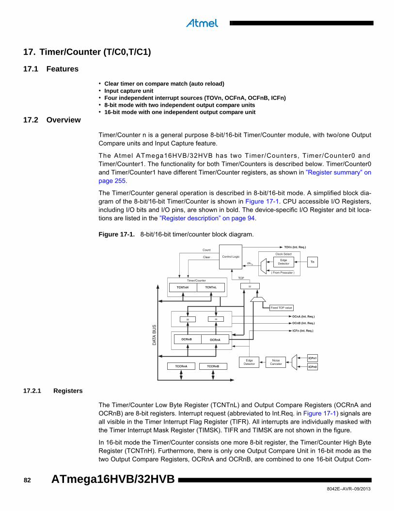
17. Timer/Counter (T/C0,T/C1)
17.1 Features
• Clear timer on compare match (auto reload)• Input capture unit• Four independent interrupt sources (TOVn, OCFnA, OCFnB, ICFn)• 8-bit mode with two independent output compare units• 16-bit mode with one independent output compare unit
17.2 Overview
Timer/Counter n is a general purpose 8-bit/16-bit Timer/Counter module, with two/one OutputCompare units and Input Capture feature.
The Atmel ATmega16HVB/32HVB has two Timer/Counters, Timer/Counter0 andTimer/Counter1. The functionality for both Timer/Counters is described below. Timer/Counter0and Timer/Counter1 have different Timer/Counter registers, as shown in ”Register summary” onpage 255.
The Timer/Counter general operation is described in 8-bit/16-bit mode. A simplified block dia-gram of the 8-bit/16-bit Timer/Counter is shown in Figure 17-1. CPU accessible I/O Registers,including I/O bits and I/O pins, are shown in bold. The device-specific I/O Register and bit loca-tions are listed in the ”Register description” on page 94.
Figure 17-1. 8-bit/16-bit timer/counter block diagram.
17.2.1 Registers
The Timer/Counter Low Byte Register (TCNTnL) and Output Compare Registers (OCRnA andOCRnB) are 8-bit registers. Interrupt request (abbreviated to Int.Req. in Figure 17-1) signals areall visible in the Timer Interrupt Flag Register (TIFR). All interrupts are individually masked withthe Timer Interrupt Mask Register (TIMSK). TIFR and TIMSK are not shown in the figure.
In 16-bit mode the Timer/Counter consists one more 8-bit register, the Timer/Counter High ByteRegister (TCNTnH). Furthermore, there is only one Output Compare Unit in 16-bit mode as thetwo Output Compare Registers, OCRnA and OCRnB, are combined to one 16-bit Output Com-
Clock Select
Timer/Counter
DAT
A B
US
OCRnB
=
TCNTnL
NoiseCanceler
ICPn0
=
EdgeDetector
Control Logic
TOP
Count
Clear
TOVn (Int. Req.)
OCnA (Int. Req.)
OCnB (Int. Req.)
ICFn (Int. Req.)
TCCRnA TCCRnB
TnEdge
Detector
( From Prescaler )
clkTn
=
OCRnA
TCNTnH
Fixed TOP value
ICPn1
828042E–AVR–09/2013
ATmega16HVB/32HVB

ATmega16HVB/32HVB
pare Register. OCRnA contains the low byte of the word and OCRnB contains the higher byte ofthe word. When accessing 16-bit registers, special procedures described in section ”Accessingregisters in 16-bit mode” on page 90 must be followed.
The Timer/Counter can be clocked internally, via the prescaler, or by an external clock source onthe Tn pin. The Clock Select logic block controls which clock source and edge the Timer/Counteruses to increment its value. The Timer/Counter is inactive when no clock source is selected. Theoutput from the Clock Select logic is referred to as the timer clock (clkTn).
17.2.2 Definitions
Many register and bit references in this section are written in general form. A lower case “n”replaces the module number, for example Timer/Counter number. A lower case “x” replaces theunit, for example OCRnx and ICPnx describes OCRnA/B and ICP1/0x . However, when usingthe register or bit defines in a program, the precise form must be used, that is, TCNT0L foraccessing Timer/Counter0 counter value and so on.
The definitions in Table 17-1 are also used extensively throughout the document.
17.3 Timer/Counter clock sources
The Timer/Counter can be clocked internally, via the prescaler, or by an external clock source.The Clock Select logic is controlled by the Clock Select (CSn2:0) bits located in the Timer/Coun-ter Control Register n B (TCCRnB), and controls which clock source and edge theTimer/Counter uses to increment its value. The Timer/Counter is inactive when no clock sourceis selected. The output from the Clock Select logic is referred to as the timer clock (clkTn). Fordetails on clock sources and prescaler, see ”Timer/Counter0 and Timer/Counter1 prescalers” onpage 79.
17.4 Counter unit
The main part of the 8-bit Timer/Counter is the counter unit. Figure 17-2 shows a block diagramof the counter and its surroundings.
Figure 17-2. Counter unit block diagram.
Table 17-1. Definitions.
BOTTOM The counter reaches the BOTTOM when it becomes 0
MAXThe counter reaches its MAXimum when it becomes 0xFF (decimal 255) in 8-bit mode or 0xFFFF (decimal 65535) in 16-bit mode
TOPThe counter reaches the TOP when it becomes equal to the highest value in the count sequence. The TOP value can be assigned to be the fixed value 0xFF/0xFFFF (MAX) or the value stored in the OCRnA Register
DATA BUS
TCNTn Control Logiccount
TOVn(Int.Req.)
Clock Select
top
TnEdge
Detector
( From Prescaler )
clkTn
838042E–AVR–09/2013
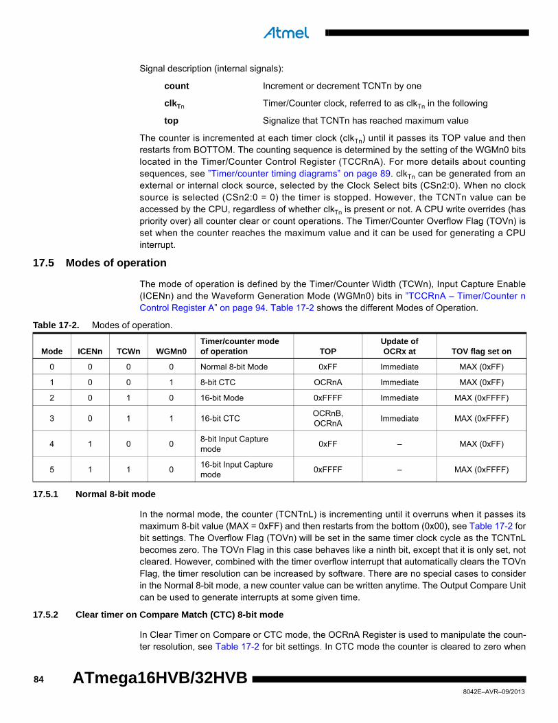
Signal description (internal signals):
count Increment or decrement TCNTn by one
clkTn Timer/Counter clock, referred to as clkTn in the following
top Signalize that TCNTn has reached maximum value
The counter is incremented at each timer clock (clkTn) until it passes its TOP value and thenrestarts from BOTTOM. The counting sequence is determined by the setting of the WGMn0 bitslocated in the Timer/Counter Control Register (TCCRnA). For more details about countingsequences, see ”Timer/counter timing diagrams” on page 89. clkTn can be generated from anexternal or internal clock source, selected by the Clock Select bits (CSn2:0). When no clocksource is selected (CSn2:0 = 0) the timer is stopped. However, the TCNTn value can beaccessed by the CPU, regardless of whether clkTn is present or not. A CPU write overrides (haspriority over) all counter clear or count operations. The Timer/Counter Overflow Flag (TOVn) isset when the counter reaches the maximum value and it can be used for generating a CPUinterrupt.
17.5 Modes of operation
The mode of operation is defined by the Timer/Counter Width (TCWn), Input Capture Enable(ICENn) and the Waveform Generation Mode (WGMn0) bits in ”TCCRnA – Timer/Counter nControl Register A” on page 94. Table 17-2 shows the different Modes of Operation.
17.5.1 Normal 8-bit mode
In the normal mode, the counter (TCNTnL) is incrementing until it overruns when it passes itsmaximum 8-bit value (MAX = 0xFF) and then restarts from the bottom (0x00), see Table 17-2 forbit settings. The Overflow Flag (TOVn) will be set in the same timer clock cycle as the TCNTnLbecomes zero. The TOVn Flag in this case behaves like a ninth bit, except that it is only set, notcleared. However, combined with the timer overflow interrupt that automatically clears the TOVnFlag, the timer resolution can be increased by software. There are no special cases to considerin the Normal 8-bit mode, a new counter value can be written anytime. The Output Compare Unitcan be used to generate interrupts at some given time.
17.5.2 Clear timer on Compare Match (CTC) 8-bit mode
In Clear Timer on Compare or CTC mode, the OCRnA Register is used to manipulate the coun-ter resolution, see Table 17-2 for bit settings. In CTC mode the counter is cleared to zero when
Table 17-2. Modes of operation.
Mode ICENn TCWn WGMn0Timer/counter mode of operation TOP
Update ofOCRx at TOV flag set on
0 0 0 0 Normal 8-bit Mode 0xFF Immediate MAX (0xFF)
1 0 0 1 8-bit CTC OCRnA Immediate MAX (0xFF)
2 0 1 0 16-bit Mode 0xFFFF Immediate MAX (0xFFFF)
3 0 1 1 16-bit CTCOCRnB, OCRnA
Immediate MAX (0xFFFF)
4 1 0 08-bit Input Capture mode
0xFF – MAX (0xFF)
5 1 1 016-bit Input Capture mode
0xFFFF – MAX (0xFFFF)
848042E–AVR–09/2013
ATmega16HVB/32HVB
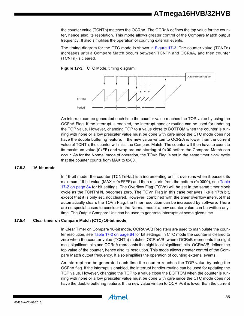
ATmega16HVB/32HVB
the counter value (TCNTn) matches the OCRnA. The OCRnA defines the top value for the coun-ter, hence also its resolution. This mode allows greater control of the Compare Match outputfrequency. It also simplifies the operation of counting external events.
The timing diagram for the CTC mode is shown in Figure 17-3. The counter value (TCNTn)increases until a Compare Match occurs between TCNTn and OCRnA, and then counter(TCNTn) is cleared.
Figure 17-3. CTC Mode, timing diagram.
An interrupt can be generated each time the counter value reaches the TOP value by using theOCFnA Flag. If the interrupt is enabled, the interrupt handler routine can be used for updatingthe TOP value. However, changing TOP to a value close to BOTTOM when the counter is run-ning with none or a low prescaler value must be done with care since the CTC mode does nothave the double buffering feature. If the new value written to OCRnA is lower than the currentvalue of TCNTn, the counter will miss the Compare Match. The counter will then have to count toits maximum value (0xFF) and wrap around starting at 0x00 before the Compare Match canoccur. As for the Normal mode of operation, the TOVn Flag is set in the same timer clock cyclethat the counter counts from MAX to 0x00.
17.5.3 16-bit mode
In 16-bit mode, the counter (TCNTnH/L) is a incrementing until it overruns when it passes itsmaximum 16-bit value (MAX = 0xFFFF) and then restarts from the bottom (0x0000), see Table17-2 on page 84 for bit settings. The Overflow Flag (TOVn) will be set in the same timer clockcycle as the TCNTnH/L becomes zero. The TOVn Flag in this case behaves like a 17th bit,except that it is only set, not cleared. However, combined with the timer overflow interrupt thatautomatically clears the TOVn Flag, the timer resolution can be increased by software. Thereare no special cases to consider in the Normal mode, a new counter value can be written any-time. The Output Compare Unit can be used to generate interrupts at some given time.
17.5.4 Clear timer on Compare Match (CTC) 16-bit mode
In Clear Timer on Compare 16-bit mode, OCRAnA/B Registers are used to manipulate the coun-ter resolution, see Table 17-2 on page 84 for bit settings. In CTC mode the counter is cleared tozero when the counter value (TCNTn) matches OCRnA/B, where OCRnB represents the eightmost significant bits and OCRnA represents the eight least significant bits. OCRnA/B defines thetop value of the counter, hence also its resolution. This mode allows greater control of the Com-pare Match output frequency. It also simplifies the operation of counting external events.
An interrupt can be generated each time the counter reaches the TOP value by using theOCFnA flag. If the interrupt is enabled, the interrupt handler routine can be used for updating theTOP value. However, changing the TOP to a value close the BOTTOM when the counter is run-ning with none or a low prescaler value must be done with care since the CTC mode does nothave the double buffering feature. If the new value written to OCRnA/B is lower than the current
TCNTn
OCnx Interrupt Flag Set
1 4Period 2 3
858042E–AVR–09/2013

value of TCNTn, the counter will miss the Compare Match. The counter will then have to count toits maximum value (0xFFFF) and wrap around starting at 0x0000 before Compare Match canoccur. As for the 16-bit Mode, the TOVn Flag is set in the same timer clock cycle that the countercounts from MAX to 0x0000.
17.5.5 8-bit Input capture mode
The Timer/Counter can be used in a 8-bit Input Capture mode, see Table 17-2 on page 84 for bitsettings. For full description, see “Input capture unit” .
17.5.6 16-bit input capture mode
The Timer/Counter can also be used in a 16-bit Input Capture mode, see Table 17-2 on page 84for bit settings. For full description, see “Input capture unit” .
17.6 Input capture unit
The Timer/Counter incorporates an Input Capture unit that can capture external events and givethem a time-stamp indicating time of occurrence. The external signal indicates an event, or mul-tiple events. For Timer/Counter0, the events can be applied via the PB0 pin (ICP00), oralternatively via the osi_posedge pin on the Oscillator Sampling Interface (ICP01). ForTimer/Counter1, the events can be applied by the Battery Protection Interrupt (ICP10) or alter-natively by the Voltage Regulator Interrupt (ICP11). The time-stamps can then be used tocalculate frequency, duty-cycle, and other features of the signal applied. Alternatively the time-stamps can be used for creating a log of the events.
The Input Capture unit is illustrated by the block diagram shown in Figure 17-4. The elements ofthe block diagram that are not directly a part of the Input Capture unit are gray shaded.
Figure 17-4. Input Capture Unit block diagram.
The Output Compare Register OCRnA is a dual-purpose register that is also used as an 8-bitInput Capture Register ICRn. In 16-bit Input Capture mode the Output Compare RegisterOCRnB serves as the high byte of the Input Capture Register ICRn. In 8-bit Input Capture modethe Output Compare Register OCRnB is free to be used as a normal Output Compare Register,but in 16-bit Input Capture mode the Output Compare Unit cannot be used as there are no freeOutput Compare Register(s). Even though the Input Capture register is called ICRn in this sec-
ICFn (Int.Req.)
WRITE ICRn (16-bit Register)
OCRnB (8-bit)
NoiseCanceler
ICPn0
EdgeDetector
TEMP (8-bit)
DATA BUS (8-bit)
OCRnA (8-bit)
TCNTn (16-bit Counter)
TCNTnH (8-bit) TCNTnL (8-bit)
ICNCn ICESn
ICPn1
ICSn
868042E–AVR–09/2013
ATmega16HVB/32HVB
ATmega16HVB/32HVB
tion, it is referring to the Output Compare Register(s). For more information on how to accessthe 16-bit registers refer to ”Accessing registers in 16-bit mode” on page 90.
When a change of the logic level (an event) occurs on the Input Capture pin (ICPx), and thischange confirms to the setting of the edge detector, a capture will be triggered. When a captureis triggered, the value of the counter (TCNTn) is written to the Input Capture Register (ICRn).The Input Capture Flag (ICFn) is set at the same system clock as the TCNTn value is copied intoInput Capture Register. If enabled (TICIEn=1), the Input Capture Flag generates an Input Cap-ture interrupt. The ICFn flag is automatically cleared when the interrupt is executed. Alternativelythe ICFn flag can be cleared by software by writing a logical one to its I/O bit location.
17.6.1 Input Capture trigger source
The default trigger source for the Input Capture unit is the I/O port PB0 in Timer/Counter0 andthe Battery Protection Interrupt in Timer/Counter1. Alternatively can the osi_posedge pin on theOscillator Sampling Interface in Timer/Counter0 and Voltage Regulator Interrupt inTimer/Counter1 be used as trigger sources. The osi_posedge pin in Timer/Counter0 ControlRegister A (TCCR0A) and the Voltage Regulator Interrupt bit in the Timer/Counter1 ControlRegister A (TCCR1A) is selected as trigger sources by setting the Input Capture Select (ICS0/1)bit. Be aware that changing trigger source can trigger a capture. The Input Capture Flag musttherefore be cleared after the change.
Both Input Capture inputs are sampled using the same technique. The edge detector is alsoidentical. However, when the noise canceler is enabled, additional logic is inserted before theedge detector, which increases the delay by four system clock cycles. An Input Capture onTimer/Counter0 can also be triggered by software by controlling the port of the PB0 pin.
17.6.2 Noise canceler
The noise canceler improves noise immunity by using a simple digital filtering scheme. Thenoise canceler input is monitored over four samples, and all four must be equal for changing theoutput that in turn is used by the edge detector.
The noise canceler is enabled by setting the Input Capture Noise Canceler (ICNCn) bit inTimer/Counter Control Register n B (TCCRnB). When enabled the noise canceler introducesadditional four system clock cycles of delay from a change applied to the input, to the update ofthe ICRn Register. The noise canceler uses the system clock and is therefore not affected by theprescaler.
17.6.3 Using the Input Capture unit
The main challenge when using the Input Capture unit is to assign enough processor capacityfor handling the incoming events. The time between two events is critical. If the processor hasnot read the captured value in the ICRn Register before the next event occurs, the ICRn will beoverwritten with a new value. In this case the result of the capture will be incorrect.
When using the Input Capture interrupt, the ICRn Register should be read as early in the inter-rupt handler routine as possible. The maximum interrupt response time is dependent on themaximum number of clock cycles it takes to handle any of the other interrupt requests.
Measurement of an external signal duty cycle requires that the trigger edge is changed aftereach capture. Changing the edge sensing must be done as early as possible after the ICRnRegister has been read. After a change of the edge, the Input Capture Flag (ICFn) must becleared by software (writing a logical one to the I/O bit location). For measuring frequency only,the trigger edge change is not required.
878042E–AVR–09/2013

Note: 1. See ”OSI – Oscillator sampling interface” on page 29 for details.
2. The noise canceler cannot be used with this source.
Note: 1. The noise canceller will filter out the input capture and it is therefore not recommended to use noise canceler with these sources.
17.7 Output compare unit
The comparator continuously compares the Timer/Counter (TCNTn) with the Output CompareRegisters (OCRnA and OCRnB), and whenever the Timer/Counter equals to the Output Com-pare Registers, the comparator signals a match. A match will set the Output Compare Flag atthe next timer clock cycle. In 8-bit mode the match can set either the Output Compare FlagOCFnA or OCFnB, but in 16-bit mode the match can set only the Output Compare Flag OCFnAas there is only one Output Compare Unit. If the corresponding interrupt is enabled, the OutputCompare Flag generates an Output Compare interrupt. The Output Compare Flag is automati-cally cleared when the interrupt is executed. Alternatively, the flag can be cleared by software bywriting a logical one to its I/O bit location. Figure 17-5 shows a block diagram of the Output Com-pare unit.
Figure 17-5. Output Compare Unit, block diagram.
17.7.1 Compare Match Blocking by TCNT0 write
All CPU write operations to the TCNTnH/L Register will block any Compare Match that occur inthe next timer clock cycle, even when the timer is stopped. This feature allows OCRnA/B to beinitialized to the same value as TCNTn without triggering an interrupt when the Timer/Counterclock is enabled.
Table 17-3. Timer/Counter0 Input Capture Source (ICS).
ICS0 Source
0 ICP00: Port PB0
1 ICP01: osi_posedge pin from OSI module (1)(2)
Table 17-4. Timer/Counter1 Input Capture Source (ICS).
ICS1 Source
0 ICP10: Battery Protection Interrupt (1)
1 ICP11: Voltage Regulator Interrupt (1)
OCFnx (Int.Req.)
= (8/16-bit Comparator )
OCRnx
DATA BUS
TCNTn
888042E–AVR–09/2013
ATmega16HVB/32HVB

ATmega16HVB/32HVB
17.7.2 Using the Output Compare Unit
Since writing TCNTnH/L will block all Compare Matches for one timer clock cycle, there are risksinvolved when changing TCNTnH/L when using the Output Compare Unit, independently ofwhether the Timer/Counter is running or not. If the value written to TCNTnH/L equals theOCRnA/B value, the Compare Match will be missed.
17.8 Timer/counter timing diagrams
The Timer/Counter is a synchronous design and the timer clock (clkTn) is therefore shown as aclock enable signal in the following figures. The figures include information on when InterruptFlags are set. Figure 17-6 contains timing data for basic Timer/Counter operation. The figureshows the count sequence close to the MAX value.
Figure 17-6. Timer/counter timing diagram, no prescaling.
Figure 17-7 shows the same timing data, but with the prescaler enabled.
Figure 17-7. Timer/counter timing diagram, with prescaler (fclk_I/O/8).
Figure 17-8 shows the setting of OCFnA and OCFnB in Normal mode.
Figure 17-8. Timer/counter timing diagram, setting of OCFnx, with prescaler (fclk_I/O/8).
clkTn(clkI/O/1)
TOVn
clkI/O
TCNTn MAX - 1 MAX BOTTOM BOTTOM + 1
TOVn
TCNTn MAX - 1 MAX BOTTOM BOTTOM + 1
clkI/O
clkTn(clkI/O/8)
OCFnx
OCRnx
TCNTn
OCRnx Value
OCRnx - 1 OCRnx OCRnx + 1 OCRnx + 2
clkI/O
clkTn(clkI/O/8)
898042E–AVR–09/2013

Figure 17-9 shows the setting of OCFnA and the clearing of TCNTn in CTC mode.
Figure 17-9. Timer/counter timing diagram, CTC mode, with prescaler (fclk_I/O/8).
17.9 Accessing registers in 16-bit mode
In 16-bit mode (the TCWn bit is set to one) the TCNTnH/L and OCRnA/B or TCNTnL/H andOCRnB/A are 16-bit registers that can be accessed by the AVR CPU via the 8-bit data bus. The16-bit register must be byte accessed using two read or write operations. The 16-bitTimer/Counter has a single 8-bit register for temporary storing of the high byte of the 16-bitaccess. The same temporary register is shared between all 16-bit registers. Accessing the lowbyte triggers the 16-bit read or write operation. When the low byte of a 16-bit register is writtenby the CPU, the high byte stored in the temporary register, and the low byte written are both cop-ied into the 16-bit register in the same clock cycle. When the low byte of a 16-bit register is readby the CPU, the high byte of the 16-bit register is copied into the temporary register in the sameclock cycle as the low byte is read.
There is one exception in the temporary register usage. In the Output Compare mode the 16-bitOutput Compare Register OCRnA/B is read without the temporary register, because the OutputCompare Register contains a fixed value that is only changed by CPU access. However, in 16-bit Input Capture mode the ICRn register formed by the OCRnA and OCRnB registers must beaccessed with the temporary register.
To do a 16-bit write, the high byte must be written before the low byte. For a 16-bit read, the lowbyte must be read before the high byte.
OCFnx
OCRnx
TCNTn(CTC)
TOP
TOP - 1 TOP BOTTOM BOTTOM + 1
clkPCK
clkTn(clkPCK /8)
908042E–AVR–09/2013
ATmega16HVB/32HVB

ATmega16HVB/32HVB
The following code examples show how to access the 16-bit timer registers assuming that nointerrupts updates the temporary register. The same principle can be used directly for accessingthe OCRnA/B registers.
Note: 1. See ”About code examples” on page 8.
The assembly code example returns the TCNTnH/L value in the r17:r16 register pair.
It is important to notice that accessing 16-bit registers are atomic operations. If an interruptoccurs between the two instructions accessing the 16-bit register, and the interrupt codeupdates the temporary register by accessing the same or any other of the 16-bit timer registers,then the result of the access outside the interrupt will be corrupted. Therefore, when both themain code and the interrupt code update the temporary register, the main code must disable theinterrupts during the 16-bit access.
Assembly code example
...
; Set TCNTn to 0x01FF
ldi r17,0x01
ldi r16,0xFF
out TCNTnH,r17
out TCNTnL,r16
; Read TCNTn into r17:r16
in r16,TCNTnL
in r17,TCNTnH
...
C code example
unsigned int i;
...
/* Set TCNTn to 0x01FF */
TCNTn = 0x1FF;
/* Read TCNTn into i */
i = TCNTn;
...
918042E–AVR–09/2013

The following code examples show how to do an atomic read of the TCNTn register contents.Reading any of the OCRn register can be done by using the same principle.
Note: 1. See ”About code examples” on page 8.
The assembly code example returns the TCNTnH/L value in the r17:r16 register pair.
Assembly code example
TIMn_ReadTCNTn:
; Save global interrupt flag
in r18,SREG
; Disable interrupts
cli
; Read TCNTn into r17:r16
in r16,TCNTnL
in r17,TCNTnH
; Restore global interrupt flag
out SREG,r18
ret
C code example
unsigned int TIMn_ReadTCNTn( void )
{
unsigned char sreg;
unsigned int i;
/* Save global interrupt flag */
sreg = SREG;
/* Disable interrupts */
_CLI();
/* Read TCNTn into i */
i = TCNTn;
/* Restore global interrupt flag */
SREG = sreg;
return i;
}
928042E–AVR–09/2013
ATmega16HVB/32HVB

ATmega16HVB/32HVB
The following code examples show how to do an atomic write of the TCNTnH/L register con-tents. Writing any of the OCRnA/B registers can be done by using the same principle.
Note: 1. See ”About code examples” on page 8.
The assembly code example requires that the r17:r16 register pair contains the value to be writ-ten to TCNTnH/L.
17.9.1 Reusing the temporary high byte register
If writing to more than one 16-bit register where the high byte is the same for all registers written,then the high byte only needs to be written once. However, note that the same rule of atomicoperation described previously also applies in this case.
Assembly code example
TIMn_WriteTCNTn:
; Save global interrupt flag
in r18,SREG
; Disable interrupts
cli
; Set TCNTn to r17:r16
out TCNTnH,r17
out TCNTnL,r16
; Restore global interrupt flag
out SREG,r18
ret
C code example
void TIMn_WriteTCNTn( unsigned int i )
{
unsigned char sreg;
unsigned int i;
/* Save global interrupt flag */
sreg = SREG;
/* Disable interrupts */
_CLI();
/* Set TCNTn to i */
TCNTn = i;
/* Restore global interrupt flag */
SREG = sreg;
}
938042E–AVR–09/2013

17.10 Register description
17.10.1 TCCRnA – Timer/Counter n Control Register A
• Bit 7 – TCWn: Timer/Counter Width
When this bit is written to one 16-bit mode is selected. Timer/Counter n width is set to 16-bitsand the Output Compare Registers OCRnA and OCRnB are combined to form one 16-bit OutputCompare Register. Because the 16-bit registers TCNTnH/L and OCRnB/A are accessed by theAVR CPU via the 8-bit data bus, special procedures must be followed. These procedures aredescribed in section ”Accessing registers in 16-bit mode” on page 90.
• Bit 6 – ICENn: Input Capture Mode Enable
The Input Capture Mode is enabled when this bit is written to one.
• Bit 5 – ICNCn: Input Capture Noise Canceler
Setting this bit activates the Input Capture Noise Canceler. When the noise canceler is acti-vated, the input from the Input Capture Source is filtered. The filter function requires foursuccessive equal valued samples of the Input Capture Source for changing its output. The InputCapture is therefore delayed by four System Clock cycles when the noise canceler is enabled.
• Bit 4 – ICESn: Input Capture Edge Select
This bit selects which edge on the Input Capture Source that is used to trigger a capture event.When the ICESn bit is written to zero, a falling (negative) edge is used as trigger, and when theICESn bit is written to one, a rising (positive) edge will trigger the capture. When a capture is trig-gered according to the ICESn setting, the counter value is copied into the Input CaptureRegister. The event will also set the Input Capture Flag (ICFn), and this can be used to cause anInput Capture Interrupt, if this interrupt is enabled.
• Bit 3 – ICSn: Input Capture Select
When written logic one, this bit enables the input capture function in Timer/Counter n to be trig-gered by the alternative Input Capture Source. To make the comparator trigger theTimer/Counter n Input Capture interrupt, the TICIEn bit in the Timer Interrupt Mask Register(TIMSK) must be set. See Table 17-3 on page 88 and Table 17-4 on page 88.
• Bits 2:1 – Reserved
These bits are reserved in the Atmel ATmega16HVB/32HVB and will always read as zero.
• Bit 0 – WGMn0: Waveform Generation Mode
This bit controls the counting sequence of the counter, the source for maximum (TOP) countervalue, see Figure 17-6 on page 89. Modes of operation supported by the Timer/Counter unit are:Normal mode (counter) and Clear Timer on Compare Match (CTC) mode (see ”Timer/countertiming diagrams” on page 89).
Bit 7 6 5 4 3 2 1 0
0x24 (0x44) TCWn ICENn ICNCn ICESn ICSn – – WGMn0 TCCRnA
Read/Write R/W R/W R/W R/W R/W R R R/W
Initial Value 0 0 0 0 0 0 0 0
948042E–AVR–09/2013
ATmega16HVB/32HVB

ATmega16HVB/32HVB
17.10.2 TCNTnL – Timer/Counter n Register Low Byte
The Timer/Counter Register TCNTnL gives direct access, both for read and write operations, tothe Timer/Counter unit 8-bit counter. Writing to the TCNTnL Register blocks (disables) the Com-pare Match on the following timer clock. Modifying the counter (TCNTnL) while the counter isrunning, introduces a risk of missing a Compare Match between TCNTnL and the OCRnx Regis-ters. In 16-bit mode the TCNTnL register contains the lower part of the 16-bit Timer/Counter nRegister.
17.10.3 TCNTnH – Timer/Counter n Register High Byte
When 16-bit mode is selected (the TCWn bit is set to one) the Timer/Counter Register TCNTnHcombined to the Timer/Counter Register TCNTnL gives direct access, both for read and writeoperations, to the Timer/Counter unit 16-bit counter. To ensure that both the high and low bytesare read and written simultaneously when the CPU accesses these registers, the access is per-formed using an 8-bit temporary high byte register (TEMP). This temporary register is shared byall the other 16-bit registers. See ”Accessing registers in 16-bit mode” on page 90.
17.10.4 OCRnA – Timer/Counter n Output Compare Register A
The Output Compare Register A contains an 8-bit value that is continuously compared with thecounter value (TCNTnL). A match can be used to generate an Output Compare interrupt.
In 16-bit mode the OCRnA register contains the low byte of the 16-bit Output Compare Register.To ensure that both the high and the low bytes are written simultaneously when the CPU writesto these registers, the access is performed using an 8-bit temporary high byte register (TEMP).This temporary register is shared by all the other 16-bit registers. See ”Accessing registers in 16-bit mode” on page 90.
17.10.5 OCRnB – Timer/Counter n Output Compare Register B
The Output Compare Register B contains an 8-bit value that is continuously compared with thecounter value (TCNTnL in 8-bit mode and TCNTnH in 16-bit mode). A match can be used togenerate an Output Compare interrupt.
Bit 7 6 5 4 3 2 1 0
0x26 (0x46) TCNTnL[7:0] TCNTnL
Read/Write R/W R/W R/W R/W R/W R/W R/W R/W
Initial Value 0 0 0 0 0 0 0 0
Bit 7 6 5 4 3 2 1 0
0x27 (0x47) TCNTnH[7:0] TCNTnH
Read/Write R/W R/W R/W R/W R/W R/W R/W R/W
Initial Value 0 0 0 0 0 0 0 0
Bit 7 6 5 4 3 2 1 0
0x28 (0x48) OCRnA[7:0] OCRnA
Read/Write R/W R/W R/W R/W R/W R/W R/W R/W
Initial Value 0 0 0 0 0 0 0 0
Bit 7 6 5 4 3 2 1 0
0x29 (0x49) OCRnB[7:0] OCRnB
Read/Write R/W R/W R/W R/W R/W R/W R/W R/W
Initial Value 0 0 0 0 0 0 0 0
958042E–AVR–09/2013
In 16-bit mode the OCRnB register contains the high byte of the 16-bit Output Compare Regis-ter. To ensure that both the high and the low bytes are written simultaneously when the CPUwrites to these registers, the access is performed using an 8-bit temporary high byte register(TEMP). This temporary register is shared by all the other 16-bit registers. See ”Accessing regis-ters in 16-bit mode” on page 90.
17.10.6 TIMSKn – Timer/Counter n Interrupt Mask Register
• Bit 3 – ICIEn: Timer/Counter n Input Capture Interrupt Enable
When this bit is written to one, and the I-flag in the Status Register is set (interrupts globallyenabled), the Timer/Counter n Input Capture interrupt is enabled. The corresponding InterruptVector (see ”Interrupts” on page 52) is executed when the ICFn flag, located in TIFRn, is set.
• Bit 2 – OCIEnB: Timer/Counter n Output Compare Match B Interrupt Enable
When the OCIEnB bit is written to one, and the I-bit in the Status Register is set, theTimer/Counter Compare Match B interrupt is enabled. The corresponding interrupt is executed ifa Compare Match in Timer/Counter occurs, that is, when the OCFnB bit is set in theTimer/Counter Interrupt Flag Register – TIFRn.
• Bit 1 – OCIEnA: Timer/Counter n Output Compare Match A Interrupt Enable
When the OCIEnA bit is written to one, and the I-bit in the Status Register is set, theTimer/Counter n Compare Match A interrupt is enabled. The corresponding interrupt is executedif a Compare Match in Timer/Counter n occurs, that is, when the OCFnA bit is set in theTimer/Counter n Interrupt Flag Register – TIFRn.
• Bit 0 – TOIEn: Timer/Counter n Overflow Interrupt Enable
When the TOIEn bit is written to one, and the I-bit in the Status Register is set, the Timer/Coun-ter n Overflow interrupt is enabled. The corresponding interrupt is executed if an overflow inTimer/Counter n occurs, that is, when the TOVn bit is set in the Timer/Counter n Interrupt FlagRegister – TIFRn.
17.10.7 TIFRn – Timer/Counter n Interrupt Flag Register
• Bits 3 – ICFn: Timer/Counter n Input Capture Flag
This flag is set when a capture event occurs, according to the setting of ICENn, ICESn and ICSnbits in the TCCRnA Register.
ICFn is automatically cleared when the Input Capture Interrupt Vector is executed. Alternatively,ICFn can be cleared by writing a logic one to its bit location.
Bit 7 6 5 4 3 2 1 0
(0x6E)(0x6F) – – – – ICIEn OCIEnB OCIEnA TOIEn TIMSKn
Read/Write R R R R R/W R/W R/W R
Initial Value 0 0 0 0 0 0 0 0
Bit 7 6 5 4 3 2 1 0
0x15 (0x35) – – – – ICFn OCFnB OCFnA TOVn TIFRn
Read/Write R R R R R/W R/W R/W R/W
Initial Value 0 0 0 0 0 0 0 0
968042E–AVR–09/2013
ATmega16HVB/32HVB

ATmega16HVB/32HVB
• Bit 2 – OCFnB: Output Compare Flag n B
The OCFnB bit is set when a Compare Match occurs between the Timer/Counter and the data inOCRnB – Output Compare Register n B. OCFnB is cleared by hardware when executing thecorresponding interrupt handling vector. Alternatively, OCFnB is cleared by writing a logic one tothe flag. When the I-bit in SREG, OCIEnB (Timer/Counter Compare B Match Interrupt Enable),and OCFnB are set, the Timer/Counter Compare Match Interrupt is executed.
The OCFnB is not set in 16-bit Output Compare mode when the Output Compare RegisterOCRnB is used as the high byte of the 16-bit Output Compare Register or in 16-bit Input Cap-ture mode when the Output Compare Register OCRnB is used as the high byte of the InputCapture Register.
• Bit 1 – OCFnA: Output Compare Flag n A
The OCFnA bit is set when a Compare Match occurs between the Timer/Counter n and the datain OCRnA – Output Compare Register n. OCFnA is cleared by hardware when executing thecorresponding interrupt handling vector. Alternatively, OCFnA is cleared by writing a logic one tothe flag. When the I-bit in SREG, OCIEnA (Timer/Counter n Compare Match Interrupt Enable),and OCFnA are set, the Timer/Counter n Compare Match Interrupt is executed.
The OCFnA is also set in 16-bit mode when a Compare Match occurs between the Timer/Coun-ter n and 16-bit data in OCRnB/A. The OCFnA is not set in Input Capture mode when the OutputCompare Register OCRnA is used as an Input Capture Register.
• Bit 0 – TOVn: Timer/Counter n Overflow Flag
The bit TOVn is set when an overflow occurs in Timer/Counter n. TOVn is cleared by hardwarewhen executing the corresponding interrupt handling vector. Alternatively, TOVn is cleared bywriting a logic one to the flag. When the SREG I-bit, TOIEn (Timer/Counter n Overflow InterruptEnable), and TOVn are set, the Timer/Counter n Overflow interrupt is executed.
978042E–AVR–09/2013

18. SPI – Serial Peripheral Interface
18.1 Features
• Full-duplex, three-wire synchronous data transfer
• Master or slave operation
• LSB first or MSB first data transfer
• Seven programmable bit rates
• End of transmission interrupt flag
• Write collision protection flag
• Wake-up from idle mode
• Double speed (CK/2) master SPI mode
18.2 Overview
The Serial Peripheral Interface (SPI) allows high-speed synchronous data transfer between theAtmel ATmega16HVB/32HVB and peripheral devices or between several AVR devices.
When the SPI is not used, power consumption can be minimized by writing the PRSPI bit inPRR0 to one. See ”PRR0 – Power Reduction Register 0” on page 40 for details on how to usethe PRSPI bit.
Figure 18-1. SPI block diagram (1).
Note: 1. Refer to ”Alternate port functions” on page 72 for SPI pin placement.
SP
I2X
SP
I2X
DIVIDER/2/4/8/16/32/64/128
988042E–AVR–09/2013
ATmega16HVB/32HVB
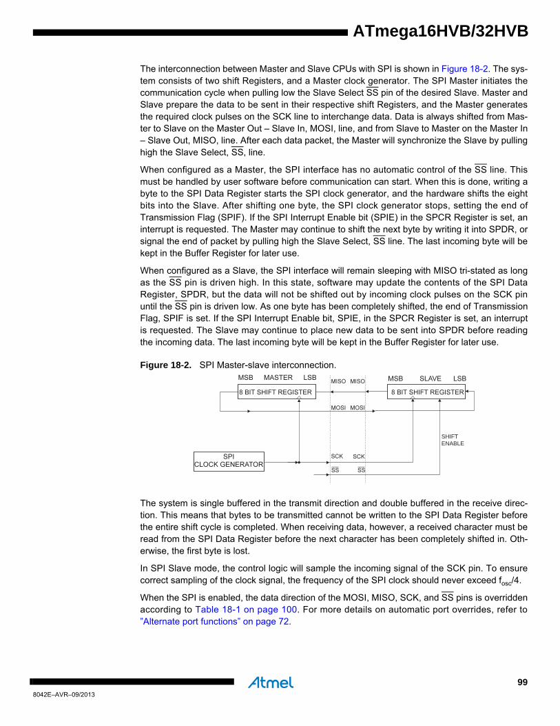
ATmega16HVB/32HVB
The interconnection between Master and Slave CPUs with SPI is shown in Figure 18-2. The sys-tem consists of two shift Registers, and a Master clock generator. The SPI Master initiates thecommunication cycle when pulling low the Slave Select SS pin of the desired Slave. Master andSlave prepare the data to be sent in their respective shift Registers, and the Master generatesthe required clock pulses on the SCK line to interchange data. Data is always shifted from Mas-ter to Slave on the Master Out – Slave In, MOSI, line, and from Slave to Master on the Master In– Slave Out, MISO, line. After each data packet, the Master will synchronize the Slave by pullinghigh the Slave Select, SS, line.
When configured as a Master, the SPI interface has no automatic control of the SS line. Thismust be handled by user software before communication can start. When this is done, writing abyte to the SPI Data Register starts the SPI clock generator, and the hardware shifts the eightbits into the Slave. After shifting one byte, the SPI clock generator stops, setting the end ofTransmission Flag (SPIF). If the SPI Interrupt Enable bit (SPIE) in the SPCR Register is set, aninterrupt is requested. The Master may continue to shift the next byte by writing it into SPDR, orsignal the end of packet by pulling high the Slave Select, SS line. The last incoming byte will bekept in the Buffer Register for later use.
When configured as a Slave, the SPI interface will remain sleeping with MISO tri-stated as longas the SS pin is driven high. In this state, software may update the contents of the SPI DataRegister, SPDR, but the data will not be shifted out by incoming clock pulses on the SCK pinuntil the SS pin is driven low. As one byte has been completely shifted, the end of TransmissionFlag, SPIF is set. If the SPI Interrupt Enable bit, SPIE, in the SPCR Register is set, an interruptis requested. The Slave may continue to place new data to be sent into SPDR before readingthe incoming data. The last incoming byte will be kept in the Buffer Register for later use.
Figure 18-2. SPI Master-slave interconnection.
The system is single buffered in the transmit direction and double buffered in the receive direc-tion. This means that bytes to be transmitted cannot be written to the SPI Data Register beforethe entire shift cycle is completed. When receiving data, however, a received character must beread from the SPI Data Register before the next character has been completely shifted in. Oth-erwise, the first byte is lost.
In SPI Slave mode, the control logic will sample the incoming signal of the SCK pin. To ensurecorrect sampling of the clock signal, the frequency of the SPI clock should never exceed fosc/4.
When the SPI is enabled, the data direction of the MOSI, MISO, SCK, and SS pins is overriddenaccording to Table 18-1 on page 100. For more details on automatic port overrides, refer to”Alternate port functions” on page 72.
SHIFTENABLE
998042E–AVR–09/2013

Note: 1. See ”Alternate functions of Port B” on page 75 for a detailed description of how to define the direction of the user defined SPI pins.
The following code examples show how to initialize the SPI as a Master and how to perform asimple transmission. DDR_SPI in the examples must be replaced by the actual Data DirectionRegister controlling the SPI pins. DD_MOSI, DD_MISO and DD_SCK must be replaced by theactual data direction bits for these pins, for example, if MOSI is placed on pin PB5, replaceDD_MOSI with DDB5 and DDR_SPI with DDRB.
Table 18-1. SPI pin overrides (1).
Pin Direction, Master SPI Direction, Slave SPI
MOSI User Defined Input
MISO Input User Defined
SCK User Defined Input
SS User Defined Input
1008042E–AVR–09/2013
ATmega16HVB/32HVB
ATmega16HVB/32HVB
Note: 1. See ”About code examples” on page 8.
Assembly code example (1)
SPI_MasterInit:
; Set MOSI and SCK output, all others input
ldi r17,(1<<DD_MOSI)|(1<<DD_SCK)
out DDR_SPI,r17
; Enable SPI, Master, set clock rate fck/16
ldi r17,(1<<SPE)|(1<<MSTR)|(1<<SPR0)
out SPCR,r17
ret
SPI_MasterTransmit:
; Start transmission of data (r16)
out SPDR,r16
Wait_Transmit:
; Wait for transmission complete
in r16,SPSR
sbrs r16,SPIF
rjmp Wait_Transmit
ret
C code example (1)
void SPI_MasterInit(void)
{
/* Set MOSI and SCK output, all others input */
DDR_SPI = (1<<DD_MOSI)|(1<<DD_SCK);
/* Enable SPI, Master, set clock rate fck/16 */
SPCR = (1<<SPE)|(1<<MSTR)|(1<<SPR0);
}
void SPI_MasterTransmit(char cData)
{
/* Start transmission */
SPDR = cData;
/* Wait for transmission complete */
while(!(SPSR & (1<<SPIF)))
;
}
1018042E–AVR–09/2013
The following code examples show how to initialize the SPI as a Slave and how to perform asimple reception.
Note: 1. See ”About code examples” on page 8.
Assembly code example (1)
SPI_SlaveInit:
; Set MISO output, all others input
ldi r17,(1<<DD_MISO)
out DDR_SPI,r17
; Enable SPI
ldi r17,(1<<SPE)
out SPCR,r17
ret
SPI_SlaveReceive:
; Wait for reception complete
in r16,SPSR
sbrs r16,SPIF
rjmp SPI_SlaveReceive
; Read received data and return
in r16,SPDR
ret
C code example (1)
void SPI_SlaveInit(void)
{
/* Set MISO output, all others input */
DDR_SPI = (1<<DD_MISO);
/* Enable SPI */
SPCR = (1<<SPE);
}
char SPI_SlaveReceive(void)
{
/* Wait for reception complete */
while(!(SPSR & (1<<SPIF)))
;
/* Return Data Register */
return SPDR;
}
1028042E–AVR–09/2013
ATmega16HVB/32HVB

ATmega16HVB/32HVB
18.3 SS pin functionality
18.3.1 Slave mode
When the SPI is configured as a Slave, the Slave Select (SS) pin is always input. When SS isheld low, the SPI is activated, and MISO becomes an output if configured so by the user. Allother pins are inputs. When SS is driven high, all pins are inputs, and the SPI is passive, whichmeans that it will not receive incoming data. Note that the SPI logic will be reset once the SS pinis driven high.
The SS pin is useful for packet/byte synchronization to keep the slave bit counter synchronouswith the master clock generator. When the SS pin is driven high, the SPI slave will immediatelyreset the send and receive logic, and drop any partially received data in the Shift Register.
18.3.2 Master mode
When the SPI is configured as a Master (MSTR in SPCR is set), the user can determine thedirection of the SS pin.
If SS is configured as an output, the pin is a general output pin which does not affect the SPIsystem. Typically, the pin will be driving the SS pin of the SPI Slave.
If SS is configured as an input, it must be held high to ensure Master SPI operation. If the SS pinis driven low by peripheral circuitry when the SPI is configured as a Master with the SS pindefined as an input, the SPI system interprets this as another master selecting the SPI as aslave and starting to send data to it. To avoid bus contention, the SPI system takes the followingactions:
1. The MSTR bit in SPCR is cleared and the SPI system becomes a Slave. As a result of the SPI becoming a Slave, the MOSI and SCK pins become inputs.
2. The SPIF Flag in SPSR is set, and if the SPI interrupt is enabled, and the I-bit in SREG is set, the interrupt routine will be executed.
Thus, when interrupt-driven SPI transmission is used in Master mode, and there exists a possi-bility that SS is driven low, the interrupt should always check that the MSTR bit is still set. If theMSTR bit has been cleared by a slave select, it must be set by the user to re-enable SPI Mastermode.
18.4 Data modes
There are four combinations of SCK phase and polarity with respect to serial data, which aredetermined by control bits CPHA and CPOL. The SPI data transfer formats are shown in Figure18-3 on page 104 and Figure 18-4 on page 104. Data bits are shifted out and latched in onopposite edges of the SCK signal, ensuring sufficient time for data signals to stabilize. This isclearly seen by summarizing Table 18-3 on page 105 and Table 18-4 on page 105, as done inTable 18-2.
Table 18-2. SPI modes.
SPI mode Conditions Leading edge Trailing edge
0 CPOL=0, CPHA=0 Sample (Rising) Setup (Falling)
1 CPOL=0, CPHA=1 Setup (Rising) Sample (Falling)
2 CPOL=1, CPHA=0 Sample (Falling) Setup (Rising)
3 CPOL=1, CPHA=1 Setup (Falling) Sample (Rising)
1038042E–AVR–09/2013

Figure 18-3. SPI transfer format with CPHA = 0.
Figure 18-4. SPI transfer format with CPHA = 1.
Bit 1Bit 6
LSBMSB
SCK (CPOL = 0)mode 0
SAMPLE IMOSI/MISO
CHANGE 0MOSI PIN
CHANGE 0MISO PIN
SCK (CPOL = 1)mode 2
SS
MSBLSB
Bit 6Bit 1
Bit 5Bit 2
Bit 4Bit 3
Bit 3Bit 4
Bit 2Bit 5
MSB first (DORD = 0)LSB first (DORD = 1)
SCK (CPOL = 0)mode 1
SAMPLE IMOSI/MISO
CHANGE 0MOSI PIN
CHANGE 0MISO PIN
SCK (CPOL = 1)mode 3
SS
MSBLSB
Bit 6Bit 1
Bit 5Bit 2
Bit 4Bit 3
Bit 3Bit 4
Bit 2Bit 5
Bit 1Bit 6
LSBMSB
MSB first (DORD = 0)LSB first (DORD = 1)
1048042E–AVR–09/2013
ATmega16HVB/32HVB

ATmega16HVB/32HVB
18.5 Register description
18.5.1 SPCR – SPI Control Register
• Bit 7 – SPIE: SPI Interrupt Enable
This bit causes the SPI interrupt to be executed if SPIF bit in the SPSR Register is set and the ifthe Global Interrupt Enable bit in SREG is set.
• Bit 6 – SPE: SPI Enable
When the SPE bit is written to one, the SPI is enabled. This bit must be set to enable any SPIoperations.
• Bit 5 – DORD: Data Order
When the DORD bit is written to one, the LSB of the data word is transmitted first.
When the DORD bit is written to zero, the MSB of the data word is transmitted first.
• Bit 4 – MSTR: Master/Slave Select
This bit selects Master SPI mode when written to one, and Slave SPI mode when written logiczero. If SS is configured as an input and is driven low while MSTR is set, MSTR will be cleared,and SPIF in SPSR will become set. The user will then have to set MSTR to re-enable SPI Mas-ter mode.
• Bit 3 – CPOL: Clock Polarity
When this bit is written to one, SCK is high when idle. When CPOL is written to zero, SCK is lowwhen idle. Refer to Figure 18-3 on page 104 and Figure 18-4 on page 104 for an example. TheCPOL functionality is summarized below:
• Bit 2 – CPHA: Clock Phase
The settings of the Clock Phase bit (CPHA) determine if data is sampled on the leading (first) ortrailing (last) edge of SCK. Refer to Figure 18-3 on page 104 and Figure 18-4 on page 104 for anexample. The CPOL functionality is summarized below:
Bit 7 6 5 4 3 2 1 0
0x2C (0x4C) SPIE SPE DORD MSTR CPOL CPHA SPR1 SPR0 SPCR
Read/Write R/W R/W R/W R/W R/W R/W R/W R/W
Initial Value 0 0 0 0 0 0 0 0
Table 18-3. CPOL functionality.
CPOL Leading edge Trailing edge
0 Rising Falling
1 Falling Rising
Table 18-4. CPHA functionality.
CPHA Leading edge Trailing edge
0 Sample Setup
1 Setup Sample
1058042E–AVR–09/2013

• Bits 1, 0 – SPR1, SPR0: SPI Clock Rate Select 1 and 0
These two bits control the SCK rate of the device configured as a Master. SPR1 and SPR0 haveno effect on the Slave. The relationship between SCK and the Oscillator Clock frequency fosc isshown in the following table:
18.5.2 SPSR – SPI Status Register
• Bit 7 – SPIF: SPI Interrupt Flag
When a serial transfer is complete, the SPIF Flag is set. An interrupt is generated if SPIE inSPCR is set and global interrupts are enabled. If SS is an input and is driven low when the SPI isin Master mode, this will also set the SPIF Flag. SPIF is cleared by hardware when executing thecorresponding interrupt handling vector. Alternatively, the SPIF bit is cleared by first reading theSPI Status Register with SPIF set, then accessing the SPI Data Register (SPDR).
• Bit 6 – WCOL: Write Collision Flag
The WCOL bit is set if the SPI Data Register (SPDR) is written during a data transfer. TheWCOL bit (and the SPIF bit) are cleared by first reading the SPI Status Register with WCOL set,and then accessing the SPI Data Register.
• Bit 5:1 – Reserved
These bits are reserved in the Atmel ATmega16HVB/32HVB and will always read as zero.
• Bit 0 – SPI2X: Double SPI Speed Bit
When this bit is written logic one the SPI speed (SCK Frequency) will be doubled when the SPIis in Master mode (see Table 18-5). This means that the minimum SCK period will be two CPUclock periods. When the SPI is configured as Slave, the SPI is only guaranteed to work at fosc/4or lower.
The SPI interface on the ATmega16HVB/32HVB is also used for program memory andEEPROM downloading or uploading. See ”Serial programming” on page 207 for serial program-ming and verification.
Table 18-5. Relationship between SCK and the oscillator frequency.
SPI2X SPR1 SPR0 SCK frequency
0 0 0 fosc/4
0 0 1 fosc/16
0 1 0 fosc/64
0 1 1 fosc/128
1 0 0 fosc/2
1 0 1 fosc/8
1 1 0 fosc/32
1 1 1 fosc/64
Bit 7 6 5 4 3 2 1 0
0x2D (0x4D) SPIF WCOL – – – – – SPI2X SPSR
Read/Write R R R R R R R R/W
Initial Value 0 0 0 0 0 0 0 0
1068042E–AVR–09/2013
ATmega16HVB/32HVB

ATmega16HVB/32HVB
18.5.3 SPDR – SPI Data Register
The SPI Data Register is a read/write register used for data transfer between the Register Fileand the SPI Shift Register. Writing to the register initiates data transmission. Reading the regis-ter causes the Shift Register Receive buffer to be read.
Bit 7 6 5 4 3 2 1 0
0x2E (0x4E) MSB LSB SPDR
Read/Write R/W R/W R/W R/W R/W R/W R/W R/W
Initial Value X X X X X X X X Undefined
1078042E–AVR–09/2013
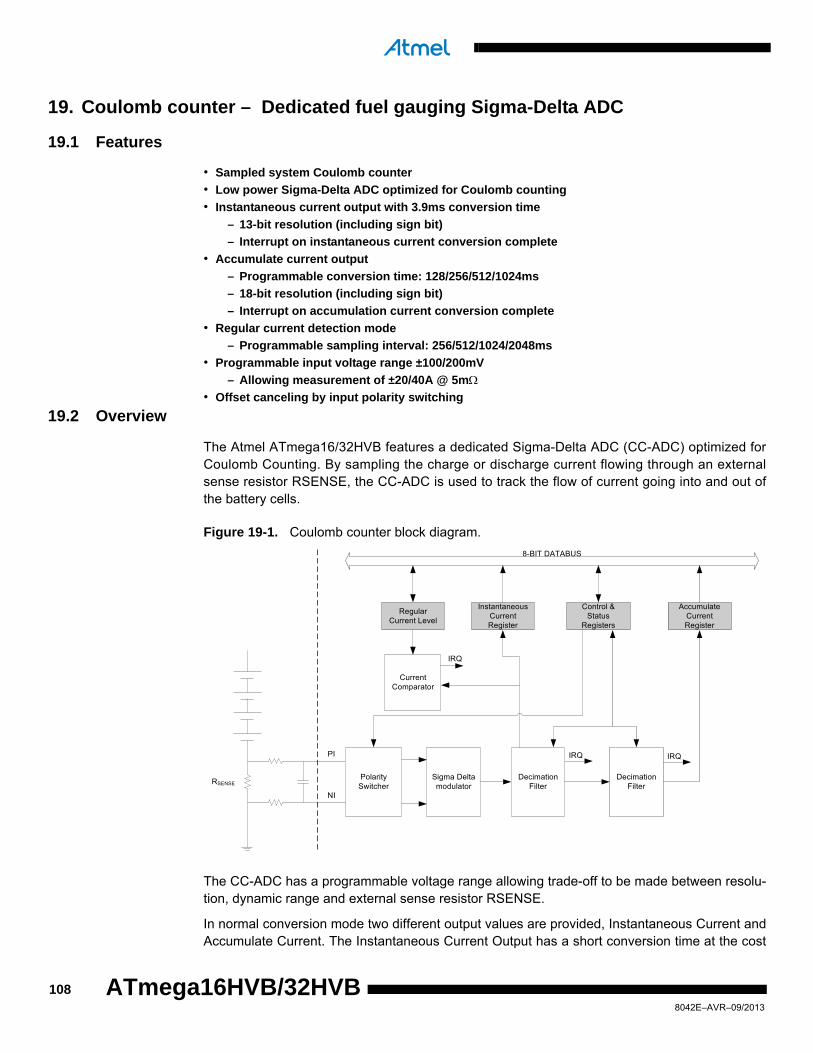
19. Coulomb counter – Dedicated fuel gauging Sigma-Delta ADC
19.1 Features
• Sampled system Coulomb counter
• Low power Sigma-Delta ADC optimized for Coulomb counting
• Instantaneous current output with 3.9ms conversion time
– 13-bit resolution (including sign bit)
– Interrupt on instantaneous current conversion complete
• Accumulate current output
– Programmable conversion time: 128/256/512/1024ms
– 18-bit resolution (including sign bit)
– Interrupt on accumulation current conversion complete
• Regular current detection mode
– Programmable sampling interval: 256/512/1024/2048ms
• Programmable input voltage range ±100/200mV
– Allowing measurement of ±20/40A @ 5m• Offset canceling by input polarity switching
19.2 Overview
The Atmel ATmega16/32HVB features a dedicated Sigma-Delta ADC (CC-ADC) optimized forCoulomb Counting. By sampling the charge or discharge current flowing through an externalsense resistor RSENSE, the CC-ADC is used to track the flow of current going into and out ofthe battery cells.
Figure 19-1. Coulomb counter block diagram.
The CC-ADC has a programmable voltage range allowing trade-off to be made between resolu-tion, dynamic range and external sense resistor RSENSE.
In normal conversion mode two different output values are provided, Instantaneous Current andAccumulate Current. The Instantaneous Current Output has a short conversion time at the cost
Sigma Delta modulator
Current Comparator
Control & Status
Registers
IRQ
8-BIT DATABUS
Regular Current Level
DecimationFilter
DecimationFilter
IRQ
IRQ
RSENSE
PI
NI
Polarity Switcher
Instantaneous Current Register
Accumulate Current Register
1088042E–AVR–09/2013
ATmega16HVB/32HVB

ATmega16HVB/32HVB
of lower resolution. The Accumulate Current Output provides a highly accurate current measure-ment for Coulomb Counting.
The CC-ADC also provides a special Regular Current detection mode. This allows ultra-lowpower operation in Power-save mode when small charge or discharge currents are flowing.
For offset cancellation the polarity of the input signal could be switched run time. Using this fea-ture, the internal CC-ADC offset could be removed. See the Atmel AVR352 application note.
19.3 Normal operation
When enabled the CC-ADC continuously measures the voltage over the external sense resistorRSENSE. Running in normal conversion mode, two data conversion outputs are provided.
• Instantaneous Conversion Result
• Accumulation Conversion Result
The Instantaneous Current conversion time is fixed to 3.9ms (typical value) allowing the outputvalue to closely follow the input. After each Instantaneous Current conversion an interrupt isgenerated if the interrupt is enabled. Data from conversion will be updated in the InstantaneousCurrent registers CADICL and CADICH simultaneously as the interrupt is given. To avoid losingconversion data, both the low and high byte must be read within a 3.9ms timing window after thecorresponding interrupt is given. When the low byte register is read, updating of the Instanta-neous Current registers and interrupts will be stopped until the high byte is read. Figure 19-2shows an Instantaneous Current conversion diagram, where DATA4 will be lost because DATA3reading is not completed within the limited period.
Figure 19-2. Instantaneous current conversions.
The Accumulate Current output is a high-resolution, high accuracy output with programmableconversion time selected by the CADAS bits in CADCSRA. The converted value is an accuratemeasurement of the average current flow during one conversion period. The CC-ADC generatesan interrupt each time a new Accumulate Current conversion has finished if the interrupt isenabled. Data from conversion will be updated in the Accumulation Current registers - CADAC0,CADAC1, CADAC2 and CADAC3 simultaneously as the interrupt is given. To avoid losing con-version data, all bytes must be read within the selected conversion period. When the lower byteregisters are read, updating of the Accumulation Current registers and interrupts will be stoppeduntil the highest byte is read. Figure 19-3 on page 110 shows an Accumulation Current conver-sion example, where DATA4 will be lost because DATA3 reading is not completed within thelimited period.
Enable
InstantaneousInterrupt
InstantaneousData
INVALID DATA DATA 1 DATA 2 DATA 3 DATA 5
Read high byte
3.9 ms 3.9 ms~12 ms settling 7.8 ms
Read low byte
1098042E–AVR–09/2013

Figure 19-3. Accumulation current conversions.
19.4 Regular current detection operation
By setting the CADSE bit in CADCSRA the CC-ADC will enter a special Regular Current Detec-tion Sampling Mode.
In this mode the CC-ADC will do one Instantaneous Current Conversion on regular samplingintervals while updating of the Accumulation Current Register is automatically disabled. Thesampling interval is controlled by writing to the CADSI bits in CADCSRA.
Each time a conversion is completed the result is compared with Regular Charge/DischargeThreshold levels specified in the CADRCC/CADRDC registers. If interrupt is enabled and thevoltage is above/below the specified limit a Regular Current Detection Interrupt will be issued.Figure 19-4 illustrates the Regular Current Detection Mode.
Figure 19-4. Regular current detection mode (CADSE=1).
19.5 Offset canceling by polarity switching
The CC-ADC offers Polarity Switching for internal offset canceling. By switching the polarity ofthe sampled input signal at selected time intervals, the internal voltage offset of the CC-ADC willcancel at the output. This feature prevents the CC-ADC from accumulating an offset error overtime.
Enable
Accumulation Interrupt
Accumulation Data
INVALID DATA DATA 1 DATA 2 DATA 3 DATA 5
Read byte 1
Read byte 2
Read byte 3
Read byte 4
125, 250, 500, or 1000 ms
125, 250, 500, or 1000 ms
1, 2, 3, or 4s settling250, 500,
1000, or 2000 ms
Measure Turn-off
~12ms ~250, 500, 1000, 2000ms
Measure
~12ms
Turn-off
~250, 500, 1000, 2000ms
Regular Current Detection Operation
Regular Current Detection Interupt
Regular Charge Current Threshold
Regular Discharge Current Threshold
Current through RSENSE
1108042E–AVR–09/2013
ATmega16HVB/32HVB

ATmega16HVB/32HVB
19.6 Configuration and usage
While the CC-ADC is converting, the CPU can enter sleep mode and wait for an interrupt. Afteradding the conversion data for the Coulomb Counting, the CPU can go back to sleep again. Thisreduces the CPU workload, and allows more time spent in low power modes, reducing powerconsumption.
To use the CC-ADC the bandgap voltage reference must be enabled separately, see ”Voltagereference and temperature sensor” on page 122.
The CC-ADC will not consume power when CADEN is cleared. It is therefore recommended toswitch off the CC-ADC whenever the Coulomb Counter or Regular Current Detection functionsare not used. The CC-ADC is automatically disabled in Power-off mode.
After the CC-ADC is enabled by setting the CADEN bit, the first four conversions do not containuseful data and should be ignored. This also applies after clearing the CADSE bit, or afterchanging the CADPOL or CADVSE bits.
The conversion times and sampling intervals are controlled by the Ultra Low Power RC Oscilla-tor (see ”Ultra Low Power RC oscillator” on page 27), and will depend on its actual frequency. Toobtain accurate coulomb counting results, the actual conversion time should be calculated.Refer to ”System clock and clock options” on page 25 for details.
19.7 Register description
19.7.1 CADCSRA – CC-ADC Control and Status Register A
• Bit 7 – CADEN: CC-ADC Enable
When the CADEN bit is cleared (zero), the CC-ADC is disabled, and any ongoing conversionswill be terminated. When the CADEN bit is set (one), the CC-ADC will continuously measure thevoltage drop over the external sense resistor RSENSE. In Power-off, the CC-ADC is alwaysdisabled.
Note that the bandgap voltage reference must be enabled separately, see ”Voltage referenceand temperature sensor” on page 122.
• Bit 6 – CADPOL: CC-ADC Polarity
The CADPOL bit is used to change input sampling polarity in the Sigma Delta Modulator. Writingthis bit to one, the polaritiy will be negative. When the bit is zero, the polarity will be positive.
• Bit 5 – CADUB: CC-ADC Update Busy
The CC-ADC operates in a different clock domain than the CPU. Whenever a new value is writ-ten to CADCSRA, CADCSRC, CADRCC or CADRDC, this value must be synchronized to theCC-ADC clock domain. Subsequent writes to these registers will be blocked during this synchro-nization. Synchronization of one of the registers will block updating of all the others. The CADUBbit will be read as one while any of these registers is being synchronized, and will be read aszero when neither register is being synchronized.
Bit 7 6 5 4 3 2 1 0
(0xE6) CADEN CADPOL CADUB CADAS1 CADAS0 CADSI1 CADSI0 CADSE CADCSRA
Read/Write R/W R/W R R/W R/W R/W R/W R/W
Initial Value 0 0 0 0 0 0 0 0
1118042E–AVR–09/2013

• Bits 4:3 – CADAS1:0: CC-ADC Accumulate Current Select
The CADAS bits select the conversion time for the Accumulate Current output as shown in theTable 19-1.
Note: 1. The actual value depends on the actual frequency of the ”Ultra Low Power RC oscillator” on page 27. See ”Electrical characteristics” on page 225.
• Bits 2:1 – CADSI1:0: CC-ADC Current Sampling Interval
The CADSI bits determine the current sampling interval for the Regular Current detection asshown in the Table 19-2.
Notes: 1. The actual value depends on the actual frequency of the ”Ultra Low Power RC oscillator” on page 27. See ”Electrical characteristics” on page 225.
2. Sampling time ~12ms.
• Bit 0 – CADSE: CC-ADC Sampling Enable
When the CADSE bit is written to one, the ongoing CC-ADC conversion is aborted and the CC-ADC enters Regular Current detection mode.
19.7.2 CADCSRB – CC-ADC Control and Status Register B
• Bits 7, 3 – Reserved
These bits are reserved in the Atmel ATmega16HVB/32HVB and will always read as zero.
• Bit 6 – CADACIE: CC-ADC Accumulate Current Interrupt Enable
When the CADACIE bit is set (one), and the I-bit in the Status Register is set (one), the CC-ADCAccumulate Current Interrupt is enabled.
Table 19-1. CC-ADC Accumulate Current Conversion Time.
CADAS1:0CC-ADC Accumulate Current
Conversion Time (1)Number of CC-ADC
clock cycles
00 128ms 4096
01 256ms 8192
10 512ms 16384
11 1s 32768
Table 19-2. CC-ADC Regular Current Sampling Interval.
CADSI1:0CC-ADC Regular Current
Sampling Interval (1)(2)Number of CC-ADC
clock cycles
00 256ms (+ sampling time) 8192 (+ sampling time)
01 512ms (+ sampling time) 16384 (+ sampling time)
10 1s (+ sampling time) 32768 (+ sampling time)
11 2s (+ sampling time) 65536 (+ sampling time)
Bit 7 6 5 4 3 2 1 0
(0xE7) – CADACIE CADRCIE CADICIE – CADACIF CADRCIF CADICIF CADCSRB
Read/Write R R/W R R/W R R/W R/W R/W
Initial Value 0 0 0 0 0 0 0 0
1128042E–AVR–09/2013
ATmega16HVB/32HVB
ATmega16HVB/32HVB
• Bit 5 – CADRCIE: CC-ADC Regular Current Interrupt Enable
When the CADRCIE bit is set (one), and the I-bit in the Status Register is set (one), the CC-ADCRegular Current Interrupt is enabled.
• Bit 4 – CADICIE: CC-ADC Instantaneous Current Interrupt Enable
When the CADICIE bit is set (one), and the I-bit in the Status Register is set (one), the CC-ADCInstantaneous Current Interrupt is enabled.
• Bit 2 – CADACIF: CC-ADC Accumulate Current Interrupt Flag
The CADACIF bit is set (one) after the Accumulate Current conversion has completed. The CC-ADC Accumulate Current Interrupt is executed if the CADACIE bit and the I-bit in SREG are set(one). CADACIF is cleared by hardware when executing the corresponding Interrupt HandlingVector. Alternatively, CADACIF is cleared by writing a logic one to the flag.
• Bit 1 – CADRCIF: CC-ADC Regular Current Interrupt Flag
The CADRCIF bit is set (one) when the absolute value of the result of the last CC-ADC conver-sion is greater than, or equal to, the compare values set by the CC-ADC RegularCharge/Discharge Current Level Registers. A positive value is compared to the Regular ChargeCurrent Level, and a negative value is compared to the Regular Discharge Current Level. TheCC-ADC Regular Current Interrupt is executed if the CADRCIE bit and the I-bit in SREG are set(one). CADRCIF is cleared by hardware when executing the corresponding Interrupt HandlingVector. Alternatively, CADRCIF is cleared by writing a logic one to the flag.
• Bit 0 – CADICIF: CC-ADC Instantaneous Current Interrupt Flag
The CADICIF bit is set (one) when a CC-ADC Instantaneous Current conversion is completed.The CC-ADC Instantaneous Current Interrupt is executed if the CADICIE bit and the I-bit inSREG are set (one). CADICIF is cleared by hardware when executing the corresponding Inter-rupt Handling vector. Alternatively, CADICIF is cleared by writing a logic one to the flag.
19.7.3 CADCSRC – CC-ADC Control and Status Register C
• Bit 7:1 – Reserved
These bits are reserved and will always read as zero.
• Bit 0 – CADVSE: CC-ADC Voltage Scaling Enable
Setting this bit enables the internal Voltage Scaling. When enabling the internal Voltage Scalingthe internal CC-ADC reference will be divided by 2, affecting the Input Voltage Range and theresulting step-size. Table 19-3 on page 113 shows the Input Voltage Range and the conversionvalue step-size for the CADVSE settings
Bit 7 6 5 4 3 2 1 0
(0xE8) – – – – – – – CADVSE CADCSRC
Read/Write R R R R R R R R/W
Initial Value 0 0 0 0 0 0 0 0
Table 19-3. Input voltage range and the conversion value step-size for the CADVSE settings.
CADVSE Voltage range Step-size CADAC Step-size CADIC
0 ±200mV 1.67µV 53.7µV
1 ±100mV 0.84µV 26.9µV
1138042E–AVR–09/2013
19.7.4 CADICH and CADICL – CC-ADC instantaneous current
When a CC-ADC Instantaneous Current conversion is complete, the result is found in these tworegisters. CADIC15:0 represents the converted result in 2's complement format. Bits 12:0 arethe 13-bit ADC result (including sign), while bit 15:13 are the sign extension bits.
When CADICL is read, the CC-ADC Instantaneous Current register is not updated until CADCHis read. Reading the registers in the sequence CADICL, CADICH will ensure that consistent val-ues are read. When a conversion is completed, both registers must be read before the nextconversion is completed, otherwise data will be lost.
19.7.5 CADAC3, CADAC2, CADAC1 and CADAC0 – CC-ADC accumulate current
The CADAC3, CADAC2, CADAC1 and CADAC0 Registers contain the Accumulate Currentmeasurements in 2’s complement format. Bits 17:0 are the 18-bit ADC result (including sign),while bit 31:18 are the sign extension bits.
When CADAC0 is read, the CC-ADC Accumulate Current register is not updated until CADAC3is read. Reading the registers in the sequence CADAC0, CADAC1, CADAC2, CADAC3 willensure that consistent values are read. When a conversion is completed, all four registers mustbe read before the next conversion is completed, otherwise data will be lost.
19.7.6 CADRCC – CC-ADC regular charge current
Bit 15 14 13 12 11 10 9 8
(0xE5) CADIC[15:8] CADICH
(0xE4) CADIC[7:0] CADICL
Bit 7 6 5 4 3 2 1 0
Read/Write R R R R R R R R
R R R R R R R R
Initial Value 0 0 0 0 0 0 0 0
0 0 0 0 0 0 0 0
Bit 31 30 29 28 27 26 25 24
23 22 21 20 19 18 17 16
15 14 13 12 11 10 9 8
7 6 5 4 3 2 1 0
(0xE3) CADAC[31:24] CADAC3
(0xE2) CADAC[23:16] CADAC2
(0xE1) CADAC[15:8] CADAC1
(0xE0) CADAC[7:0] CADAC0
Read/Write R R R R R R R R
R R R R R R R R
R R R R R R R R
Initial Value 0 0 0 0 0 0 0 0
0 0 0 0 0 0 0 0
0 0 0 0 0 0 0 0
Bit 7 6 5 4 3 2 1 0
(0xE9) CADRCC[7:0] CADRCC
Read/Write R/W R/W R/W R/W R/W R/W R/W R/W
Initial Value 0 0 0 0 0 0 0 0
1148042E–AVR–09/2013
ATmega16HVB/32HVB

ATmega16HVB/32HVB
The CC-ADC Regular Charge Current Register determines the threshold level for the RegularCharge Current detection. When the result of a CC-ADC Instantaneous Current conversion ispositive with a value greater than, or equal to, the Regular Charge Current level, the CC-ADCRegular Current Interrupt Flag is set.
The value in this register defines the eight least significant bits of the Regular Charge Currentlevel in 2's complement format, where the most significant bits of the Regular Charge Currentlevel are always zero. The programmable range for the Regular Charge Current level is given inthe Table 19-4.
Note: 1. Values in the table are shown with the CADVSE set to both 0 and 1.
The CC-ADC Regular Charge Current Register does not affect the setting of the CC-ADC Con-version Complete Interrupt Flag.
19.7.7 CADRDC – CC-ADC regular discharge current
The CC-ADC Regular Discharge Current Register determines the threshold level for the RegularDischarge Current detection. When the result of a CC-ADC Instantaneous Current conversion isnegative with an absolute value greater than, or equal to, the Regular Discharge Current level,the CC-ADC Regular Current Interrupt Flag is set.
The value in this register defines the eight least significant bits of the Regular Discharge Currentlevel in 2's complement format, where the most significant bits of the Regular Discharge Currentlevel are always one. The programmable range for the Regular Discharge Current level is givenin the Table 19-5 on page 115.
Note: Values in the table are shown with the CADVSE set to both 0 and 1.
The CC-ADC Regular Discharge Current Register does not affect the setting of the CC-ADCConversion Complete Interrupt Flag.
Table 19-4. Programmable range for the regular charge current level (1).
Minimum Maximum Step Size
Voltage (µV) 0 13696/6848 53.7/26.9
Current (mA)
RSENSE = 1m 0 13696/6848 53.7/26.9
RSENSE = 5m 0 2740/1370 10.7/5.4
RSENSE = 10m 0 1370/685 5.3/2.7
Bit 7 6 5 4 3 2 1 0
(0xEA) CADRDC[7:0] CADRDC
Read/Write R/W R/W R/W R/W R/W R/W R/W R/W
Initial Value 0 0 0 0 0 0 0 0
Table 19-5. Programmable range for the regular discharge current level.
Minimum Maximum Step size
Voltage (µV) 0 13696/6848 53.7/26.9
Current (mA)
RSENSE = 1m 0 13696/6848 53.7/26.9
RSENSE = 5m 0 2740/1370 10.7/5.4
RSENSE = 10m 0 1370/685 5.3/2.7
1158042E–AVR–09/2013

20. Voltage ADC – 7-channel general purpose 12-bit Sigma-Delta ADC
20.1 Features
• 12-bit resolution
• 519µs conversion time @ 1MHz clkVADC
• Four differential input channels for cell voltage measurements
• Three single ended input channels
• 0.2× pre-scaling of cell voltages
• Interrupt on V-ADC conversion complete
20.2 Overview
The Atmel ATmega16HVB/32HVB features a 12-bit Sigma-Delta ADC.
The Voltage ADC (V-ADC) is connected to seven different sources through the Input Multi-plexer. There are four differential channels for Cell Voltage measurements. These channels arescaled 0.2× to comply with the Full Scale range of the V-ADC. In addition there are three singleended channels referenced to SGND. One channel is for measuring the internal temperaturesensor VPTAT and two channels for measuring the voltage at ADC0 and ADC1.
When the V-ADC is not used, power consumption can be minimized by writing the PRVADC bitin PRR0 to one. See ”PRR0 – Power Reduction Register 0” on page 40 for details on how to usethe PRVADC bit.
Figure 20-1. Voltage ADC block schematic.
20.3 Operation
To enable V-ADC conversions, the V-ADC Enable bit, VADEN, in V-ADC Control and StatusRegister – VADCSR must be set. If this bit is cleared, the V-ADC will be switched off, and anyongoing conversions will be terminated. The V-ADC is automatically disabled in Power-save and
V-ADC CONVERSION COMPLETE IRQ
8-BIT DATA BUS
V-ADC MULTIPLEXERSEL. REG (VADMUX)
V-ADC CONTROL ANDSTATUS REG (VADCSR)
V-ADC DATA REGISTER(VADCL/ADCH)
VA
DC
CIE
VA
DC
CIF
12-BIT SIGMA-DELTA ADC
INPUTMUX
V-ADC CONTROL
ADC1/SGND
ADC0/SGND
VTEMP
PV2
PV1
NV
Note: The shaded signals are scaled by 0.2, other signals are scaled by 1.0 VREF SGND
PV3
PV4
1168042E–AVR–09/2013
ATmega16HVB/32HVB
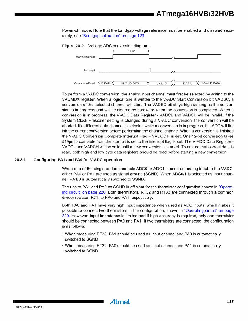
ATmega16HVB/32HVB
Power-off mode. Note that the bandgap voltage reference must be enabled and disabled sepa-rately, see ”Bandgap calibration” on page 123.
Figure 20-2. Voltage ADC conversion diagram.
To perform a V-ADC conversion, the analog input channel must first be selected by writing to theVADMUX register. When a logical one is written to the V-ADC Start Conversion bit VADSC, aconversion of the selected channel will start. The VADSC bit stays high as long as the conver-sion is in progress and will be cleared by hardware when the conversion is completed. When aconversion is in progress, the V-ADC Data Register - VADCL and VADCH will be invalid. If theSystem Clock Prescaler setting is changed during a V-ADC conversion, the conversion will beaborted. If a different data channel is selected while a conversion is in progress, the ADC will fin-ish the current conversion before performing the channel change. When a conversion is finishedthe V-ADC Conversion Complete Interrupt Flag – VADCCIF is set. One 12-bit conversion takes519µs to complete from the start bit is set to the interrupt flag is set. The V-ADC Data Register -VADCL and VADCH will be valid until a new conversion is started. To ensure that correct data isread, both high and low byte data registers should be read before starting a new conversion.
20.3.1 Configuring PA1 and PA0 for V-ADC operation
When one of the single ended channels ADC0 or ADC1 is used as analog input to the VADC,either PA0 or PA1 are used as signal ground (SGND). When ADC0/1 is selected as input chan-nel, PA1/0 is automatically switched to SGND.
The use of PA1 and PA0 as SGND is efficient for the thermistor configuration shown in ”Operat-ing circuit” on page 220. Both thermistors, RT32 and RT33 are connected through a commondivider resistor, R31, to PA0 and PA1 respectively.
Both PA0 and PA1 have very high input impedance when used as ADC inputs, which makes itpossible to connect two thermistors in the configuration, shown in ”Operating circuit” on page220. However, input impedance is limited and if high accuracy is required, only one thermistorshould be connected between PA0 and PA1. If two thermistors are connected, the configurationis as follows:
• When measuring RT33, PA1 should be used as input channel and PA0 is automatically switched to SGND
• When measuring RT32, PA0 should be used as input channel and PA1 is automatically switched to SGND
Start Conversion
Interrupt
Conversion Result INVALID DATAINVALID DATAOLD DATA VA L I D D ATA
519µs
1178042E–AVR–09/2013

20.3.2 Cell inputs
The V-ADC features one input channel for each battery cell to be able to measure each cell indi-vidually and to measure the total battery voltage through the input pins NV, PV1, PV2, PV3 andPV4. Note that the internal Cell Balancing uses the same pins to bypass balancing current (see”Cell balancing” on page 151) for details for balancing the battery cells. When balancing a cellthe V-ADC should not do conversion on the selected channel, as the internal Cell balancing willaffect the conversion result.
The V-ADC is designed to operate on PV1 pin voltages above 2V. If the battery cell voltage onPV1 input falls below 2V the upper cell voltage appears to be lower than the its actual value. Toavoid that cells get potentially overcharged software should keep the cells in balance using theinternal Cell Balancing. See ”Cell balancing” on page 151 for details.
When not using all the cell inputs, the unused cells should be connected to the cell below. Anexample external coupling in 3-cell mode is shown in Figure 20-3. Note that even if the input isnot used, it is recommended to connect the input through an external resistance to limit inversecoupling current. This is to be able to protect the battery if cells are reversed coupled duringproduction.
Figure 20-3. A 3-cell mode connection.
ATmega16HVB/32HVB
R
R
PV4
PV3
PV2
PV1
NV
R
C
C
C
R
R
1188042E–AVR–09/2013
ATmega16HVB/32HVB

ATmega16HVB/32HVB
20.4 Register description
20.4.1 VADMUX – V-ADC Multiplexer Selection Register
• Bit 7:4 – Reserved
These bits are reserved in the Atmel ATmega16HVB/32HVB and will always read as zero.
• Bit 3:0 – VADMUX[3:0]: V-ADC Channel Selection Bits
The VADMUX bits determine the V-ADC channel selection. See Table 20-1.
20.4.2 VADCSR – V-ADC Control and Status Register
• Bit 7:4 – Reserved
These bits are reserved in the ATmega16HVB/32HVB and will always read as zero.
• Bit 3 – VADEN: V-ADC Enable
Writing this bit to one enables V-ADC conversion. By writing it to zero, the V-ADC is turned off.Turning the V-ADC off while a conversion is in progress will terminate this conversion. Note thatthe bandgap voltage reference must be enabled separately, see ”Bandgap calibration” on page123.
Bit 7 6 5 4 3 2 1 0
(0x7C) – – – – VADMUX3 VADMUX2 VADMUX1 VADMUX0 VADMUX
Read/Write R R R R R/W R/W R/W R/W
Initial Value 0 0 0 0 0 0 0 0
Table 20-1. VADMUX channel selection.
VADMUX[3:0] Channel selected Scale
0000 RESERVED –
0001 CELL1 0.2
0010 CELL2 0.2
0011 CELL3 0.2
0100 CELL4 0.2
0101 VTEMP 1.0
0110 ADC0 1.0
0111 ADC1 1.0
1000...1111 RESERVED –
Bit 7 6 5 4 3 2 1 0
(0x7A) – – – – VADEN VADSC VADCCIF VADCCIE VADCSR
Read/Write R R R R R/W R/W R/W R/W
Initial Value 0 0 0 0 0 0 0 0
1198042E–AVR–09/2013

• Bit 2 – VADSC: Voltage ADC Start Conversion
Write this bit to one to start a new conversion of the selected channel.
VADSC will read as one as long as the conversion is not finished. When the conversion is com-plete, it returns to zero. Writing zero to this bit has no effect. VADSC will automatically becleared when the VADEN bit is written to zero.
• Bit 1 – VADCCIF: V-ADC Conversion Complete Interrupt Flag
This bit is set when a V-ADC conversion completes and the data registers are updated. The V-ADC Conversion Complete Interrupt is executed if the VADCCIE bit and the I-bit in SREG areset. VADCCIF is cleared by hardware when executing the corresponding interrupt handling vec-tor. Alternatively, VADCCIF is cleared by writing a logical one to the flag. Beware that if doing aRead-Modify-Write on VADCSR, a pending interrupt can be lost.
• Bit 0 – VADCCIE: V-ADC Conversion Complete Interrupt Enable
When this bit is written to one and the I-bit in SREG is set, the V-ADC Conversion CompleteInterrupt is activated.
20.4.3 VADCL and VADCH – V-ADC Data Register
When a V-ADC conversion is complete, the result is found in these two registers. To ensure thatcorrect data is read, both high and low byte data registers should be read before starting a newconversion.
• VADC11:0: V-ADC Conversion Result
These bits represent the result from the conversion.
To obtain the best absolute accuracy for the cell voltage measurements, gain and offset com-pensation is required. Factory calibration values are stored in the device signature row, refer tosection ”Reading the signature row from software” on page 195 for details. The cell voltage inmV is given by:
The voltage on the ADCn is given by:
Bit 15 14 13 12 11 10 9 8
(0x79) – – – – VADC[11:8] VADCH
(0x78) VADC[7:0] VADCL
7 6 5 4 3 2 1 0
Read/Write R R R R R R R R
R R R R R R R R
Initial Value 0 0 0 0 0 0 0 0
0 0 0 0 0 0 0 0
Celln[mV](VADCH/L VADC CellnOffset) VADC Celln Gain Calibration Word–
16384--------------------------------------------------------------------------------------------------------------------------------------------------------------------------------------=
ADCn[mV]1
10------
(VADCH/L VADC ADCn Offset) VADC ADCn Gain Calibration Word–16384
----------------------------------------------------------------------------------------------------------------------------------------------------------------------------------------------=
1208042E–AVR–09/2013
ATmega16HVB/32HVB
ATmega16HVB/32HVB
When performing a Vtemp conversion, the result must be adjusted by the factory calibrationvalue stored in the signature row, refer to section ”Reading the signature row from software” onpage 195 for details. The absolute temperature in Kelvin is given by:
20.4.4 DIDR0 – Digital Input Disable Register 0
• Bits 7:2 – Reserved
These bits are reserved for future use. To ensure compatibility with future devices, these bitsmust be written to zero when DIDR0 is written.
• Bit 1:0 – PA1DID:PA0DID: Digital Input Disable
When this bit is written logic one, the digital input buffer on the corresponding Port A pin is dis-abled. The corresponding PIN Register bit will always read as zero when this bit is set. When ananalog signal is applied to the PA1:0 pin and the digital input from this pin is not needed, this bitshould be written logic one to reduce power consumption in the digital input buffer.
T(K)VADCH/L VPTAT CAL
16384---------------------------------------------------------------=
Bit 7 6 5 4 3 2 1 0
(0x7E) – – – – – – PA1DID PA0DID DIDR0
Read/Write R R R R R R R/W R/W
Initial Value 0 0 0 0 0 0 0 0
1218042E–AVR–09/2013

21. Voltage reference and temperature sensor
21.1 Features
• Accurate voltage reference of 1.100V
• Voltage reference calibration interface
• Internal temperature sensor
• External decoupling for optimum noise performance
• Short circuit detection on the external decoupling pin
• Low power consumption
21.2 Overview
The Atmel ATmega16HVB/32HVB features a highly accurate low power On-chip Bandgap Ref-erence Voltage, VREF of 1.100V. This reference voltage is used as reference for the On-chipVoltage Regulator, the Brown-out Detector, the internal Cell Balancing, the Battery Protection,the V-ADC and the CC-ADC. Figure 21-1 shows an overview of the On-chip voltage reference.
Figure 21-1. Bandgap reference voltage.
In addition to the Bandgap Reference Voltage, the Voltage Reference includes a Calibration Unitthat enables run time calibration of the Reference Voltage, an On-chip temperature sensor formonitoring the die temperature, and a Bandgap Short Detector to detect short circuit conditionson the external VREF pin for highest safety.
21.3 Operation
When the device is in power-off state, the Voltage Reference will be switched off. After a Power-on reset condition the Voltage Reference will automatically be enabled.
BG CalibrationBG Control and Status
8-bit databus
Bangap Referencew/ temperature sensor
BG Short Detector
VREF
VREFGND
IRQ
VPTAT 1.1V BGBuffer
1228042E–AVR–09/2013
ATmega16HVB/32HVB
ATmega16HVB/32HVB
By default the Bandgap Buffer will be enabled as the buffered reference voltage is used as refer-ence for the Battery Protection, the internal Cell Balancing, the V-ADC and the CC-ADC. If anyof these modules are enabled the Bandgap Buffer must be enabled, otherwise it is recom-mended to disable the buffer by writing to the BGD bit in BGCSR to save power. Note that theBandgap Buffer needs settling time before the voltage is stable. For details on settling time, see“Bandgap buffer settling time” .
To ensure that the battery protection has safe operation condition, the Voltage Referenceincludes a Short-circuit Detector. The Bandgap Short Detector continuously monitors the internal1.100V reference voltage against the VREF pin voltage to detect potentially external short condi-tions to VCC or GND. If an external short condition is detected, the Bandgap Short CircuitDetection is capable of interrupting and waking up the CPU from any sleep mode. If a BandgapShort-circuit condition occurs software should immediately disable the C-FET and D-FET. If noexternal protection is provided to detect such a condition it is recommended to always enablethis feature, by setting the BGSCDE bit in the Bandgap Control and Status Register.
The Temperature Sensor generates a voltage Proportional-To-Absolute-Temperature, VPTAT.This voltage is connected to the multiplexer at the V-ADC input and it can be used for runtimecompensation of temperature drift in both the voltage reference and the On-chip Oscillator. Toget the absolute temperature in degrees Kelvin, the measured VPTAT voltage must be scaledwith the VPTAT factory calibration value stored in the signature row. See ”Reading the signaturerow from software” on page 195 for details. See ”Electrical characteristics” on page 225 fordetails on temperature accuracy.
21.4 Bandgap calibration
To guarantee ultra low temperature drift the Voltage Reference includes two calibration registersthat should be initialized by software after reset. See ”Register description” on page 124 fordetails. Changing values to the BGCCR IO register will change the nominal value of the Band-gap Reference Voltage, while changing values to the BGCRR IO register trims the temperaturegradient of the bandgap reference.
When the calibration registers are changed it will affect both the Voltage Regulator output andBOD-level. The BOD will react quickly to new detection levels, while the regulator will adjust thevoltage more slowly, depending on the size of the external decoupling capacitor. To avoid that aBOD-reset is issued when calibration is done, it is recommended to change the values of theBGCC and BGCR bits stepwise, with a step size of one, and with a hold-off time between eachstep. See ”Electrical characteristics” on page 225 for details on hold-off time.
Changing VREF will influence the conversion results for the V-ADC and CC-ADC. It is thereforenot recommended to do V-ADC and CC-ADC conversions while calibrating the bandgap.
21.5 Bandgap buffer settling time
After the Voltage Reference have been enabled it needs a settling time before the voltage is sta-ble. The settling time depends on the size of the external decoupling capacitor. With 1µFexternal capacitor a minimum settling time of 2ms should be used. Until settling is done it is notrecommended to enable the NFET driver (OC/OD or enter DUVR operation), Battery Protection,V-ADC or CC-ADC.
Settling time is needed when the Buffer is enabled by software, or after a reset condition.
1238042E–AVR–09/2013
21.6 Register description
21.6.1 BGCCR – Bandgap Calibration C Register
• Bits 7:6 – Reserved
These bits are reserved and will always read as zero.
• Bit 5:0 – BGCC[5:0]: BG Calibration of PTAT Current
These bits are used for trimming of the nominal value of the bandgap reference voltage. Thesebits are binary coded. Minimum VREF: 000000, maximum VREF: 111111. Step size is approxi-mately 2mV. The application software should read the Atmel factory calibration value and store itto the BGCCR register. See ”Reading the signature row from software” on page 195 for details.
21.6.2 BGCRR – Bandgap Calibration R Register
• Bit 7:0 – BGCR[7:0]: BG Calibration of Resistor ladder
These bits are used for temperature gradient adjustment of the bandgap reference. Figure 21-2on page 125 illustrates VREF as a function of temperature. VREF has a positive temperaturecoefficient at low temperatures and negative temperature coefficient at high temperatures.Depending on the process variations, the top of the VREF curve may be located at higher orlower temperatures. To minimize the temperature drift in the temperature range of interest,BGCRR is used to adjust the top of the curve towards the centre of the temperature range ofinterest. The BGCRR bits are thermometer coded, resulting in 9 possible settings: 00000000,00000001, 00000011, 00000111, … , 11111111. The value 00000000 shifts the top of the VREFcurve to the highest possible temperature, and the value 11111111 shifts the top of the VREFcurve to the lowest possible temperature. The application software should read the Atmel factorycalibration value and store it to the BGCRR register. See ”Reading the signature row from soft-ware” on page 195 for details.
Bit 7 6 5 4 3 2 1 0
(0xD0) – – BGCC5 BGCC4 BGCC3 BGCC2 BGCC1 BGCC0 BGCCR
Read/Write R R R/W R/W R/W R/W R/W R/W
Initial Value 0 0 0 0 0 0 0 0
Bit 7 6 5 4 3 2 1 0
(0xD1) BGCR7 BGCR6 BGCR5 BGCR4 BGCR3 BGCR2 BGCR1 BGCR0 BGCRR
Read/Write R/W R/W R/W R/W R/W R/W R/W R/W
Initial Value 0 0 0 0 1 1 1 1
1248042E–AVR–09/2013
ATmega16HVB/32HVB
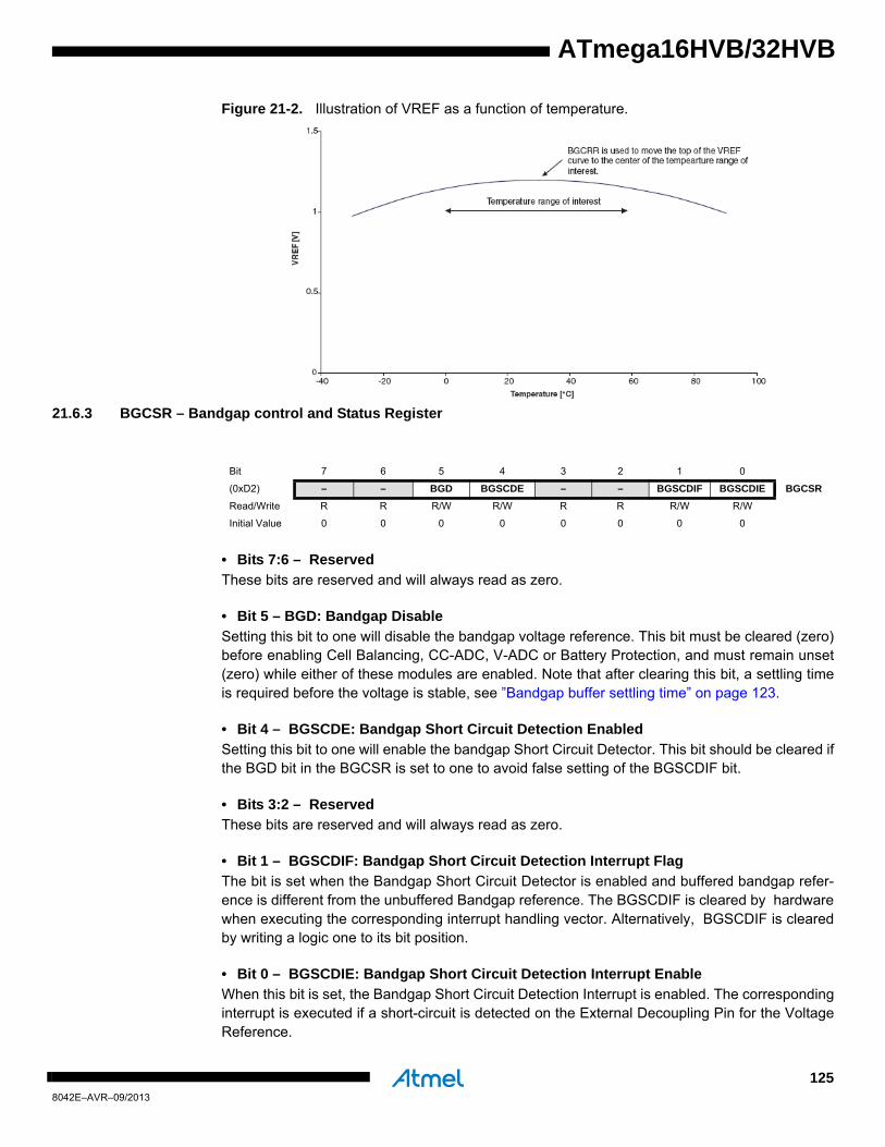
ATmega16HVB/32HVB
Figure 21-2. Illustration of VREF as a function of temperature.
21.6.3 BGCSR – Bandgap control and Status Register
• Bits 7:6 – Reserved
These bits are reserved and will always read as zero.
• Bit 5 – BGD: Bandgap Disable
Setting this bit to one will disable the bandgap voltage reference. This bit must be cleared (zero)before enabling Cell Balancing, CC-ADC, V-ADC or Battery Protection, and must remain unset(zero) while either of these modules are enabled. Note that after clearing this bit, a settling timeis required before the voltage is stable, see ”Bandgap buffer settling time” on page 123.
• Bit 4 – BGSCDE: Bandgap Short Circuit Detection Enabled
Setting this bit to one will enable the bandgap Short Circuit Detector. This bit should be cleared ifthe BGD bit in the BGCSR is set to one to avoid false setting of the BGSCDIF bit.
• Bits 3:2 – Reserved
These bits are reserved and will always read as zero.
• Bit 1 – BGSCDIF: Bandgap Short Circuit Detection Interrupt Flag
The bit is set when the Bandgap Short Circuit Detector is enabled and buffered bandgap refer-ence is different from the unbuffered Bandgap reference. The BGSCDIF is cleared by hardwarewhen executing the corresponding interrupt handling vector. Alternatively, BGSCDIF is clearedby writing a logic one to its bit position.
• Bit 0 – BGSCDIE: Bandgap Short Circuit Detection Interrupt Enable
When this bit is set, the Bandgap Short Circuit Detection Interrupt is enabled. The correspondinginterrupt is executed if a short-circuit is detected on the External Decoupling Pin for the VoltageReference.
Bit 7 6 5 4 3 2 1 0
(0xD2) – – BGD BGSCDE – – BGSCDIF BGSCDIE BGCSR
Read/Write R R R/W R/W R R R/W R/W
Initial Value 0 0 0 0 0 0 0 0
1258042E–AVR–09/2013

22. Charger detect
22.1 Features
• Operates directly from VFET supply
• Detects when a charger is connected or disconnected by monitoring the BATT pin
• Controls the operation state of the device by automatically enable/disable the internal voltage
regulator
• Automatically disabled when discharge FET is ON
• Interrupt wake-up from all sleep modes
22.2 Overview
The Charger Detect module has two main functions:
• Control the device operating state (power-off or normal operation)
• Detect when a charger is connected/disconnected
Figure 22-1 shows a block diagram of the Charger Detect module.
Figure 22-1. Charger Detect block diagram.
Charger Detectw/Power-on Reset
VFET
+
-
IRQ
POWER_OFF
POR
8-BIT DATABUS
DFET_EN
BLOD
SLEEP (power-off)
BATT
Charger Detect Interrupt Logic
CHARGER_PRESENT
1268042E–AVR–09/2013
ATmega16HVB/32HVB

ATmega16HVB/32HVB
22.3 Operation
The Charger Detect module is supplied directly from the VFET pin. When operating, the ChargerDetect will monitor the voltage of the BATT pin and detect whether a charger is present or not.When the voltage on the BATT pin is above the Charger Detect Threshold level VPOT (see ”Elec-trical characteristics” on page 225) the CHARGER_PRESENT signal will be high. This signal isedge detected to generate interrupt when a charger is connected or disconnected.
The Charger Detect module will operate as long as the Discharge FET is disabled and is able todetect a charger in all sleep modes including Power-off.
22.3.1 Device operating state
The Charger Detect module controls the operating state of the Atmel ATmega16HVB/32HVB byenabling/disabling the Voltage Regulator, which supplies the rest of the internal logic on thechip.
If the chip is in Power-off state the Charger Detect will keep the Voltage Regulator disabledallowing only the Charger Detect module itself to operate. To be able to start from a Power-offstate a charge voltage above VPOT has to be applied at the BATT pin. When a charger is con-nected the Charger Detect module will automatically start the Voltage Regulator. When theVREG voltage rises, a Power-on Reset (POR) is given and the chip enters normal operatingmode after a reset delay corresponding to TTOUT. For details on POR, see ”Power-on reset andcharger connect” on page 43.
When the ATmega16HVB/32HVB is running in normal operation mode software or hardwarecould take the chip into Power-off state. For details on entering power-off by software, see”Power-off mode” on page 38. To protect the device against software malfunctions theATmega16HVB/32HVB has a Black-out Detector (BLOD). When a Black-out condition occursthe Charger Detect will take the chip automatically into Power-off. For details on Black-outDetection, see ”Voltage regulator” on page 129.
Note that after a software power-off the BATT pin voltage has to fall below the Charger Detectthreshold limit, VPOT, before the chip is able to re-enable the Voltage Regulator and start-up thedevice.
22.3.2 Interrupt logic
When the ATmega16HVB/32HVB is running in normal operation mode, the Charger Detect iscapable of giving an interrupt to the CPU if a charger is connected/disconnected or both. Inter-rupt is enabled/disabled by writing to the CHGDIE bit in the ”CHGDCSR – Charger DetectControl and Status Register” on page 128.
Interrupt is given when a charger is connected, disconnected or both depending on interruptsense control settings. Selecting the correct interrupt sensing is done by writing to the CHGDISCbits in the ”CHGDCSR – Charger Detect Control and Status Register” on page 128.
Charger Detect interrupt works asynchronous and will wake the CPU from any sleep mode.
The Charger Detect is automatically disabled/enabled when changing the state of the DischargeFET, and any interrupt that occurs when enabling or disabling the Discharge FET has to becarefully interpreted.
• When enabling the Discharge-FET the Charger Detect module is automatically disabled. When disabling the charger detect module a charger appear to be disconnected even if a charger is present
1278042E–AVR–09/2013
• When disabling the Charge-FET the Charger Detect module is automatically enabled and a charger appear to be connected
22.4 Register description
22.4.1 CHGDCSR – Charger Detect Control and Status Register
• Bit 7:5 – Reserved
These bits are reserved and will always read as zero.
• Bit 4 – BATTPVL: BATT pin Voltage Level
BATTPVL will read one as long when the Charger Detect module is enabled and the BATT pinvoltage is above the VPOT level. Otherwise the BATTPVL will read zero.
• Bit 3:2 – CHGDISC[1:0]: Charger Detect Interrupt Sense Control
Edges in the CHARGER_PRESENT signal shown in Figure 22-1 on page 126 are used to acti-vate a Charger Detect Interrupt if the SREG I-flag and the interrupt enable bit in CHGDCSR areset. By writing the CHGDISC bits to the values shown in Table 22-1 the condition generatinginterrupt is configured. When changing the CHGDISC bits, an interrupt can occur. Therefore, it isrecommended to first disable the Interrupt by clearing its CHGDIE bit in the CHGDICSR Regis-ter. Finally, the Charger Detect interrupt flag should be cleared by writing a logical one toCHGDIF bit before the interrupt is re-enabled.
• Bit 1 – CHGDIF: Charger Detect Interrupt Flag
Depending on the configuration of the CHGDISC bits in the CHGDCSR, this bit is set when acharger is either connected or disconnected. The Charger Detect Interrupt is executed if theCHGDIE bit and the I-bit in SREG are set. This bit is cleared by hardware when executing thecorresponding interrupt handling vector or alternatively by writing a logical one to the CHGDIF. Itis recommended to write this bit to one when setting CHGDIE.
• Bit 0 – CHGDIE: Charger Detect Interrupt Enable
When the CHGDIE bit is set (one), and the I-bit in the Status Register is set (one), the ChargerDetect Interrupt is enabled.
Bit 7 6 5 4 3 2 1 0
(0xD4) – – – BATTPVL CHGDISC1 CHGDISC0 CHGDIF CHGDIE CHGDCSR
Read/Write R R R R R/W R/W R/W R/W
Initial Value 0 0 0 0 0 0 0 0
Table 22-1. Charger Detect Interrupt Sense Control.
CHGISC[1:0] Detection
00 Charger Connect
01 Charger Disconnect
10 Charger Connect/Disconnect
11 None
1288042E–AVR–09/2013
ATmega16HVB/32HVB

ATmega16HVB/32HVB
23. Voltage regulator
23.1 Features
• Input voltage from 4V - 18V
• Fixed output voltage of 3.3V
• Battery pack short detection
• Black-out detection (BLOD)
23.2 Overview
The Atmel ATmega16HVB/32HVB get its voltage supply through the VFET terminal. Operatingrange at the VFET terminal is 4V - 18V. The on-chip LDO regulator regulates the VFET terminaldown to 3.3V, which is a suitable supply voltage for the internal logic, I/O lines and analog cir-cuitry. Figure 23-1 illustrates the Voltage Regulator.
Figure 23-1. Voltage regulator.
To ensure safe operating condition the Voltage Regulator has built in protection mechanisms toprotect the internal circuitry if the voltage drops on either the input or output terminal. The Regu-lator Monitoring includes.
• Battery Pack Short Detector
• Black-out Detector
An external decoupling capacitor (CREG) of minimum 1µF is needed to ensure stable regulatoroperation. The same capacitor also serves as a reservoir capacitor to ensure that the chip isable to operate for some time without voltage at the VFET terminal.
Regulator Monitor and Control Interface
LDO Regulator
Databus
VFET
DISABLE VFET
IRQ
BLOD
POWER-OFF
CREG
VREG
Battery Short Detect
ROCR
Black-out Detect
EN
AB
LE
1298042E–AVR–09/2013
23.3 Regulator start-up
When the chip is in power-off mode the Voltage Regulator will be off and there will be no con-nection between VFET and VREG.
The regulator is started when the Charger Detect module detects that a charger is connected(for details on Charger Detect, see ”Charger detect” on page 126). When starting the regulatorthe Voltage Regulator will stay in a force mode where the VREG output is raised against theVFET input voltage. As VREG increases to the target voltage level the regulator will automati-cally enter regulation mode, with a stable output voltage of nominally 3.3V. Figure 11-2 on page44, in System Control and Reset illustrates the start-up sequence from power-off.
23.4 Battery pack short detection
The Voltage Regulator will continuously monitor the operating condition at the VFET terminal. Ifthe voltage at VFET drops below the Regulator Short-circuit Level (RSCL), see ”Electrical char-acteristics” on page 225, the Voltage Regulator enters the Battery Pack Short mode. In thismode, VFET is disconnected from VREG to avoid a quick drop in the voltage regulator output.When the voltage regulator enters this mode, the chip will be completely powered by the exter-nal reservoir capacitor (CREG). This allows the chip to operate a certain time without enteringBOD reset, even if the VFET voltage is too low for the voltage regulator to operate.
An interrupt is issued when the regulator enters Battery Pack Short mode, if the ROCWIE bit inROCR Register is set. This allows actions to be taken to reduce power consumption and henceprolonging the time that CREG can be used to power the chip.
In a typical short-circuit situation, VFET will drop as a consequence of high current consumption,and recover as soon as the Battery Protection module has disabled the FETs. Hence CREGshould be dimensioned so that the chip can sustain operation without entering BOD reset, untilthe FETs are disabled either by HW or SW.
To minimize power consumption when the Voltage Regulator enters the Battery Pack Shortmode, the chip should enter Power-save sleep mode as soon as possible after the ROCWIFinterrupt is detected. The Watchdog Timer should be configured to wake up the CPU after a timethat is considered safe, see application note AVR132 for use of enhanced Watchdog Timer.Software should then check the status of the ROC flag. If the ROCS flag is cleared, normal oper-ation may be resumed.
23.5 Black-out detection
To ensure that the internal logic has safe operating condition, the Voltage Regulator has built-inBlack-Out Detector (BLOD). If the voltage at the VREG pin drops below the Black-out DetectionLevel, VBLOT, the chip will automatically enter Power-off mode.
1308042E–AVR–09/2013
ATmega16HVB/32HVB
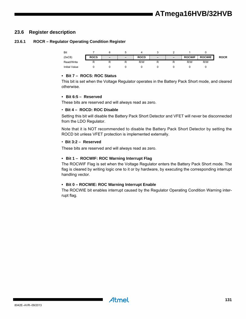
ATmega16HVB/32HVB
23.6 Register description
23.6.1 ROCR – Regulator Operating Condition Register
• Bit 7 – ROCS: ROC Status
This bit is set when the Voltage Regulator operates in the Battery Pack Short mode, and clearedotherwise.
• Bit 6:5 – Reserved
These bits are reserved and will always read as zero.
• Bit 4 – ROCD: ROC Disable
Setting this bit will disable the Battery Pack Short Detector and VFET will never be disconnectedfrom the LDO Regulator.
Note that it is NOT recommended to disable the Battery Pack Short Detector by setting theROCD bit unless VFET protection is implemented externally.
• Bit 3:2 – Reserved
These bits are reserved and will always read as zero.
• Bit 1 – ROCWIF: ROC Warning Interrupt Flag
The ROCWIF Flag is set when the Voltage Regulator enters the Battery Pack Short mode. Theflag is cleared by writing logic one to it or by hardware, by executing the corresponding interrupthandling vector.
• Bit 0 – ROCWIE: ROC Warning Interrupt Enable
The ROCWIE bit enables interrupt caused by the Regulator Operating Condition Warning inter-rupt flag.
Bit 7 6 5 4 3 2 1 0
(0xC8) ROCS – – ROCD – – ROCWIF ROCWIE ROCR
Read/Write R R R R/W R R R/W R/W
Initial Value 0 0 0 0 0 0 0 0
1318042E–AVR–09/2013
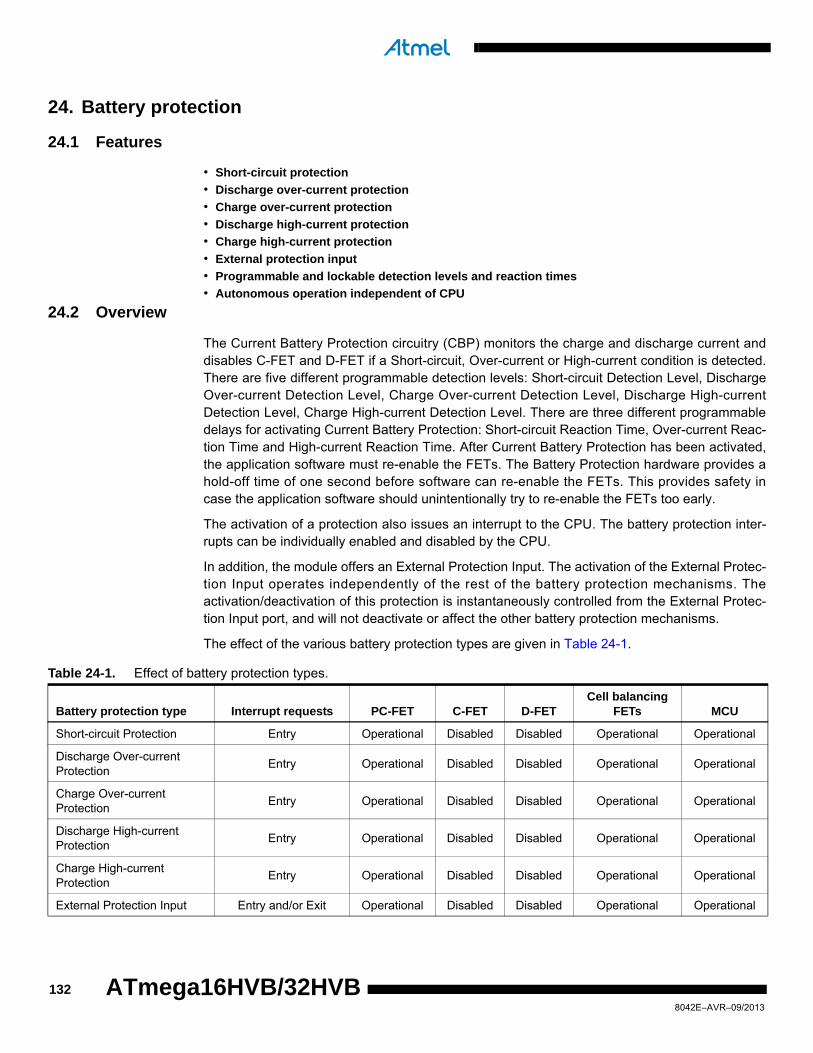
24. Battery protection
24.1 Features
• Short-circuit protection
• Discharge over-current protection
• Charge over-current protection
• Discharge high-current protection
• Charge high-current protection
• External protection input
• Programmable and lockable detection levels and reaction times
• Autonomous operation independent of CPU
24.2 Overview
The Current Battery Protection circuitry (CBP) monitors the charge and discharge current anddisables C-FET and D-FET if a Short-circuit, Over-current or High-current condition is detected.There are five different programmable detection levels: Short-circuit Detection Level, DischargeOver-current Detection Level, Charge Over-current Detection Level, Discharge High-currentDetection Level, Charge High-current Detection Level. There are three different programmabledelays for activating Current Battery Protection: Short-circuit Reaction Time, Over-current Reac-tion Time and High-current Reaction Time. After Current Battery Protection has been activated,the application software must re-enable the FETs. The Battery Protection hardware provides ahold-off time of one second before software can re-enable the FETs. This provides safety incase the application software should unintentionally try to re-enable the FETs too early.
The activation of a protection also issues an interrupt to the CPU. The battery protection inter-rupts can be individually enabled and disabled by the CPU.
In addition, the module offers an External Protection Input. The activation of the External Protec-tion Input operates independently of the rest of the battery protection mechanisms. Theactivation/deactivation of this protection is instantaneously controlled from the External Protec-tion Input port, and will not deactivate or affect the other battery protection mechanisms.
The effect of the various battery protection types are given in Table 24-1.
Table 24-1. Effect of battery protection types.
Battery protection type Interrupt requests PC-FET C-FET D-FETCell balancing
FETs MCU
Short-circuit Protection Entry Operational Disabled Disabled Operational Operational
Discharge Over-currentProtection
Entry Operational Disabled Disabled Operational Operational
Charge Over-currentProtection
Entry Operational Disabled Disabled Operational Operational
Discharge High-currentProtection
Entry Operational Disabled Disabled Operational Operational
Charge High-currentProtection
Entry Operational Disabled Disabled Operational Operational
External Protection Input Entry and/or Exit Operational Disabled Disabled Operational Operational
1328042E–AVR–09/2013
ATmega16HVB/32HVB

ATmega16HVB/32HVB
24.3 Operation
The Current Battery Protections (CBP) monitors the cell current by sampling the shunt resistorvoltage at the PPI/NNI input pins. A differential operational amplifier amplifies the voltage with asuitable gain. The output from the operational amplifier is compared to an accurate, programma-ble On-chip voltage reference by an Analog Comparator. If the shunt resistor voltage is abovethe Detection level for a time longer than the corresponding Protection Reaction Time, the chipactivates Current Protection. A sampled system clocked by the internal ULP Oscillator is usedfor Short-circuit, Over-current, and High-current Protection. This ensures a reliable clock source,offset cancellation and low power consumption.
24.3.1 Short-circuit protection
The Short-circuit detection is provided to enable a fast response time to very large dischargecurrents. If the voltage at the PPI/NNI pins is above the Short-circuit Detection Level for a periodlonger than Short-circuit Reaction Time, the Short-circuit Protection is activated.
When the Short-circuit Protection is activated, the external D-FET and C-FET are disabled and aCurrent Protection Timer is started. This timer ensures that the D-FET and C-FET are disabledfor at least one second. The application software must then set the DFE and CFE bits in the FETControl and Status Register to re-enable normal operation. If the D-FET is re-enabled before thecause of the short-circuit condition is removed, the Short-circuit Protection will be activatedagain.
24.3.2 Discharge over-current protection
If the voltage at the PPI/NNI pins is above the Discharge Over-current Detection level for a timelonger than Over-current Protection Reaction Time, the chip activates Discharge Over-currentProtection.
When the Discharge Over-current Protection is activated, the external D-FET and C-FET aredisabled and a Current Protection Timer is started. This timer ensures that the FETs are dis-abled for at least one second. The application software must then set the DFE and CFE bits inthe FET Control and Status Register to re-enable normal operation. If the D-FET is re-enabledwhile the loading of the battery still is too large, the Discharge Over-current Protection will beactivated again.
24.3.3 Charge over-current protection
If the voltage at the PPI/NNI pins is above the Charge Over-current Detection level for a timelonger than Over-current Protection Reaction Time, the chip activates Charge Over-currentProtection.
When the Charge Over-current Protection is activated, the external D-FET and C-FET are dis-abled and a Current Protection Timer is started. This timer ensures that the FETs are disabledfor at least one second. The application software must then set the DFE and CFE bits in the FETControl and Status Register to re-enable normal operation. If the C-FET is re-enabled and thecharger continues to supply too high currents, the Charge Over-current Protection will be acti-vated again.
24.3.4 Discharge high-current protection
If the voltage at the PPI/NNI pins is above the Discharge High-current Detection level for a timelonger than High-current Protection Reaction Time, the chip activates Discharge High-currentProtection.
1338042E–AVR–09/2013

When the Discharge High-current Protection is activated, the external D-FET and C-FET are dis-abled and a Current Protection Timer is started. This timer ensures that the FETs are disabledfor at least one second. The application software must then set the DFE and CFE bits in the FETControl and Status Register to re-enable normal operation. If the D-FET is re-enabled while theloading of the battery still is too large, the Discharge High-current Protection will be activatedagain.
24.3.5 Charge high-current protection
If the voltage at the PPI/NNI pins is above the Charge High-current Detection level for a time lon-ger than High-current Protection Reaction Time, the chip activates Charge High-currentProtection.
When the Charge High-current Protection is activated, the external D-FET and C-FET are dis-abled and a Current Protection Timer is started. This timer ensures that the FETs are disabledfor at least one second. The application software must then set the DFE and CFE bits in the FETControl and Status Register to re-enable normal operation. If the C-FET is re-enabled and thecharger continues to supply too high currents, the Charge High-current Protection will be acti-vated again.
The Short-circuit, Over-current and High-current Protection parameters are programmable toadapt to different types of batteries. The parameters are set by writing to I/O Registers. TheParameter Registers can be locked after the initial configuration, prohibiting any further updatesuntil the next Hardware Reset.
Refer to ”Register description” on page 137 for register descriptions of battery protection.
24.4 External protection input
The External Protection Input uses the alternate port function of the General Purpose High Vot-lage I/O to automatically disabling the external Charge and Discharge-FET. For details, see”High voltage I/O ports” on page 62.
Using this together with the External Interrupt (see ”External interrupt characteristics” on page230) features a highly flexible solution for the customer and it allows the user to customize anexternal protection scheme suitable for battery applications.
The External Protection Input disables both the C-FET and D-FET immediately when the voltageon EXTPROT pin is pulled high (logic ‘1’). It is also used to disable DUVR mode if DUVR modeis enabled. Note that, unlike a Battery Protection event, the External Protection input does notaffect the status of the FCSR (CFE, DFE, DUVRD, and CPS) bits. When the ‘high’ condition dis-appears, the FET disabling is released immediately. DUVR mode is automatically re-entered ifpreviously enabled.
The feature is automatically enabled when the chip starts up, and can be disabled before lockingthe BPCR register. When locking the BPCR register, the External Protection feature is alsolocked.
When External Protection Input is enabled, an override enable signal is set to EXTPROT pinconfiguring the pin as digital input. The port may be set up to give an interrupt when the pinvalue changes, and the protection status can be read from the port register.
Note that the External Protection Input is default enabled. This means that after reset (and dur-ing reset) the port is default overridden to digital input, independent of the port register setting.
1348042E–AVR–09/2013
ATmega16HVB/32HVB

ATmega16HVB/32HVB
The user must disable the External Protection Input in the BPCR register before the port can beused as a normal port.
Also during the reset sequence, the External Protection Input may disable the FETs. Conse-quently, if the External Protection feature is not used and DUVR mode is enabled in reset, theExternal Protection input must be held low until disabled by SW.
It is recommended that the external interrupt on the External Protection Input port is configuredto ‘any edge’ to generate an interrupt to the microcontroller when using this feature, indicatingthat the FET protection status has changed. By reading the pin register, the External Protectionstatus can be determined. If the pin register is set, it means that External Protection is triggedand the FET control signals in FCSR (CFE, DFE and DUVRD) are overridden and the FETs aredisabled. In the opposite case, External Protection violation is not present.
To ensure a safe exit from the External Protection Input condition, the FETs and DUVR modeshould be disabled by SW when an External Protection condition is detected. This enables soft-ware to completely control when the FETs are switched ON again.
Short pulses on the EXTPROT pin, for instance caused by temporary high voltages on the BATTpin when connecting a charger, may trigger the External Protection Input (refer to ”Operating cir-cuit” on page 220). However if the SW does not take any action, the C-FET and D-FET will bere-enabled automatically once the External Protection condition disappears.
Figure 24-1. External protection input example.
FCSR [CFE]
FCSR [DFE]
PC0
INT0
OC
OD
1358042E–AVR–09/2013

24.5 Optimizing usage for low power consumption
In order to reduce power consumption, Short-circuit, Discharge High-current and DischargeOver-current Protection are automatically deactivated when the D-FET is disabled. The ChargeOver-current and Charge High-current Protection are disabled when the C-FET is disabled. Notehowever that Charge Over-current Protection and Charge High-current Protection are neverautomatically disabled when the chip is operated in DUVR mode.
Also note that none of the current protections are deactivated by the External Protection Input.To save power during an External Protection event, DFE and CFE in the FCSR register shouldbe cleared and make sure that the chip is not operating in DUVR mode.
1368042E–AVR–09/2013
ATmega16HVB/32HVB

ATmega16HVB/32HVB
24.6 Battery protection CPU interface
The Battery Protection CPU Interface is illustrated in Figure 24-2.
Figure 24-2. Battery protection CPU interface.
Each protection originating from the Current Battery Protection module has an Interrupt Flag.Each Flag can be read and cleared by the CPU, and each flag has an individual interrupt enable.All enabled flags are combined into a single battery protection interrupt request to the CPU. Thisinterrupt can wake up the CPU from any operation mode, except Power-off. The interrupt flagsare cleared by writing a logic ‘1’ to their bit locations from the CPU. An interrupt event for theExternal Protection Input can be generated by enabling the external interrupt for the input port.
24.7 Register description
24.7.1 BPPLR – Battery Protection Parameter Lock Register
• Bit 7:2 – Reserved
These bits are reserved and will always read as zero.
• Bit 1 – BPPLE: Battery Protection Parameter Lock Enable
• Bit 0 – BPPL: Battery Protection Parameter Lock
The BPCR, BPHCTR, BPOCTR, BPSCTR, BPDHCD, BPCHCD, BPDOCD, BPCOCD andBPSCD Battery Protection registers can be locked from any further software updates. Once
5/
5/
10/
InterruptRequest
InterruptAcknowledge
FETControl
Current Battery
Protection
Battery ProtectionControl Register
Battery ProtectionTiming Register
Battery ProtectionLevel Register
Battery ProtectionParameter Lock
Register
PPI
NNI
LOCK? LOCK? LOCK?
8-BIT DATA BUS
Power-off
BatteryProtectionInterruptRegister
CurrentProtection
EXTPROT
Bit 7 6 5 4 3 2 1 0
(0xFE) – – – – – – BPPLE BPPL BPPLR
Read/Write R R R R R R R/W R/W
Initial Value 0 0 0 0 0 0 0 0
1378042E–AVR–09/2013
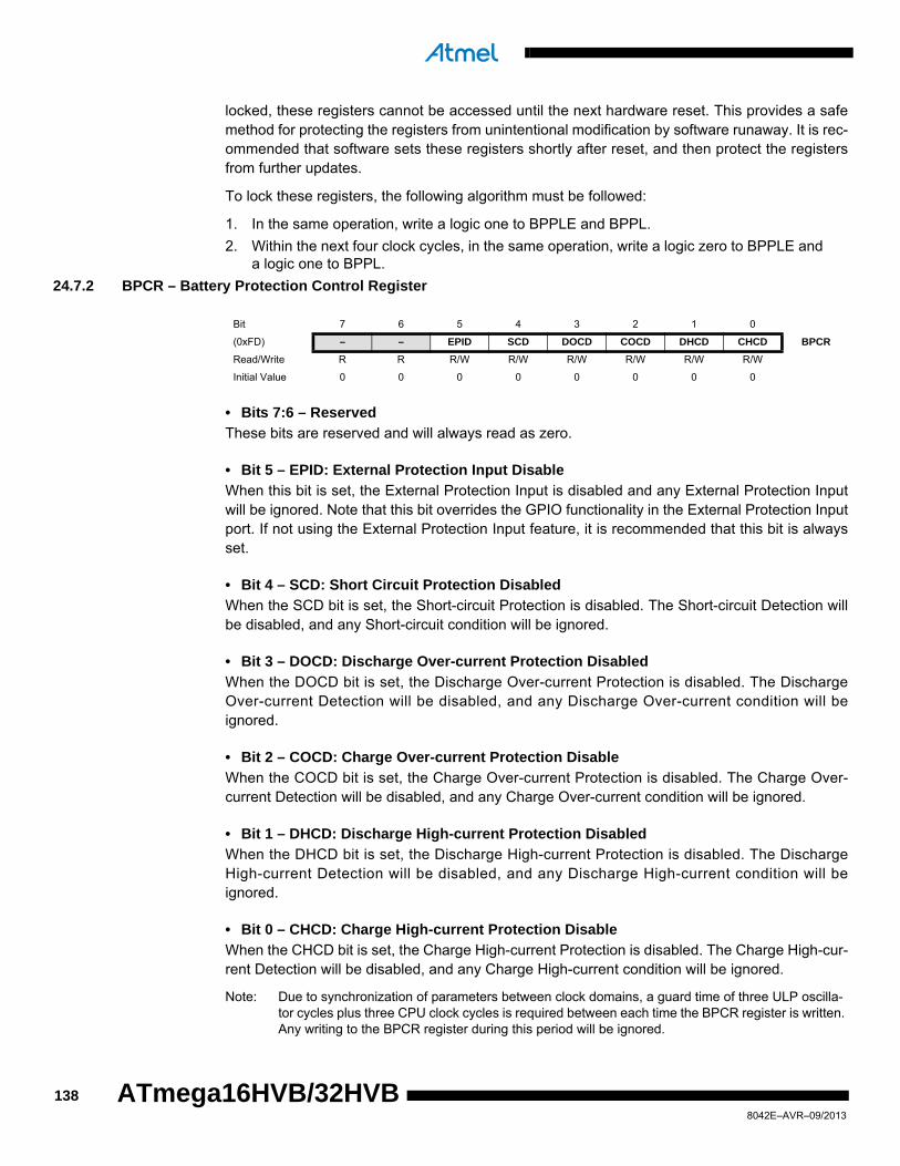
locked, these registers cannot be accessed until the next hardware reset. This provides a safemethod for protecting the registers from unintentional modification by software runaway. It is rec-ommended that software sets these registers shortly after reset, and then protect the registersfrom further updates.
To lock these registers, the following algorithm must be followed:
1. In the same operation, write a logic one to BPPLE and BPPL.
2. Within the next four clock cycles, in the same operation, write a logic zero to BPPLE and a logic one to BPPL.
24.7.2 BPCR – Battery Protection Control Register
• Bits 7:6 – Reserved
These bits are reserved and will always read as zero.
• Bit 5 – EPID: External Protection Input Disable
When this bit is set, the External Protection Input is disabled and any External Protection Inputwill be ignored. Note that this bit overrides the GPIO functionality in the External Protection Inputport. If not using the External Protection Input feature, it is recommended that this bit is alwaysset.
• Bit 4 – SCD: Short Circuit Protection Disabled
When the SCD bit is set, the Short-circuit Protection is disabled. The Short-circuit Detection willbe disabled, and any Short-circuit condition will be ignored.
• Bit 3 – DOCD: Discharge Over-current Protection Disabled
When the DOCD bit is set, the Discharge Over-current Protection is disabled. The DischargeOver-current Detection will be disabled, and any Discharge Over-current condition will beignored.
• Bit 2 – COCD: Charge Over-current Protection Disable
When the COCD bit is set, the Charge Over-current Protection is disabled. The Charge Over-current Detection will be disabled, and any Charge Over-current condition will be ignored.
• Bit 1 – DHCD: Discharge High-current Protection Disabled
When the DHCD bit is set, the Discharge High-current Protection is disabled. The DischargeHigh-current Detection will be disabled, and any Discharge High-current condition will beignored.
• Bit 0 – CHCD: Charge High-current Protection Disable
When the CHCD bit is set, the Charge High-current Protection is disabled. The Charge High-cur-rent Detection will be disabled, and any Charge High-current condition will be ignored.
Note: Due to synchronization of parameters between clock domains, a guard time of three ULP oscilla-tor cycles plus three CPU clock cycles is required between each time the BPCR register is written. Any writing to the BPCR register during this period will be ignored.
Bit 7 6 5 4 3 2 1 0
(0xFD) – – EPID SCD DOCD COCD DHCD CHCD BPCR
Read/Write R R R/W R/W R/W R/W R/W R/W
Initial Value 0 0 0 0 0 0 0 0
1388042E–AVR–09/2013
ATmega16HVB/32HVB
ATmega16HVB/32HVB
24.7.3 BPSCTR – Battery Protection Short-current Timing Register
• Bit 7 – Reserved
This bit is reserved in the Atmel ATmega16HVB/32HVB and will always read as zero.
• Bit 6:0 – SCPT[6:0]: Short-current Protection Timing
These bits control the delay of the Short-circuit Protection. The Short-circuit Timing can be setwith a step size of 62.5µs as shown in Table 24-2.
Notes: 1. The actual value depends on the actual frequency of the ”Ultra Low Power RC oscillator” on page 27. See ”Electrical characteristics” on page 225.
2. Initial value: SCPT[0x10](1ms).3. An additional delay Td can be expected after enabling the Discharge FET due to initialization
of the protection circuit. With nomial ULP frequency this delay is maximum 86µs.
Note: Due to synchronization of parameters between clock domains, a guard time of 3 ULP oscillator cycles + 3 CPU clock cycles is required between each time the BPSCTR register is written. Any writing to the BPSCTR register during this period will be ignored.
24.7.4 BPOCTR – Battery Protection Over-current Timing Register
• Bit 7:6 – Reserved
These bits are reserved in the ATmega16HVB/32HVB and will always read as zero.
• Bit 5:0 – OCPT[5:0]: Over-current Protection Timing
These bits control the delay of the Over-circuit Protection. The Over-current Timing can be setwith a step size of 0.5 ms as shown in Table 24-3 on page 140.
Bit 7 6 5 4 3 2 1 0
(0xFA) – SCPT[6:0] BPSCTR
Read/Write R R/W R/W R/W R/W R/W R/W R/W
Initial Value 0 0 0 1 0 0 0 0
Table 24-2. Short-circuit Protection Reaction Time. SCPT[6:0] with corresponding Short-cir-cuit Delay Time.
Short-circuit Protection Reaction Time (1)
SCPT[6:0] (2) Typ
0x00 (15.5µs - 70.5µs) + Td (3)
0x01 (15.5µs - 70.5µs) + Td (3)
0x02 (78.0µs - 133.0µs) + Td (3)
0x03 (140.5µs - 195.5µs) + Td (3)
... ...
0x7E (7.83ms - 7.88ms) + Td (3)
0x7F (7.89ms - 7.95ms) + Td (3)
Bit 7 6 5 4 3 2 1 0
(0xFB) – – OCPT[5:0] BPOCTR
Read/Write R R R/W R/W R/W R/W R/W R/W
Initial Value 0 0 0 0 0 0 1 0
1398042E–AVR–09/2013
Notes: 1. The actual value depends on the actual frequency of the ”Ultra Low Power RC oscillator” on page 27. See ”Electrical characteristics” on page 225.
2. Initial value.3. An additional delay Td can be expected after enabling the corresponding FET. This is related
to the initialization of the protection circuitry. For the Discharge Over-Current protection, this applies when enabling the Discharge FET. For Charge Over-Current protection, this applies when enabling the Charge FET. With nominal ULP frequency this delay is maximum 0.1ms.
Note: Due to synchronization of parameters between clock domains, a guard time of three ULP oscilla-tor cycles plus three CPU clock cycles is required between each time the BPOCTR register is written. Any writing to the BPOCTR register during this period will be ignored.
24.7.5 BPHCTR – Battery protection high-current timing register
• Bit 7:6 – Reserved
These bits are reserved in the Atmel ATmega16HVB/32HVB and will always read as zero.
• Bit 5:0 – HCPT[5:0]: High-current protection timing
These bits control the delay of the High-circuit Protection. The High-current Timing can be setwith a step size of 2 ms as shown in Table 24-4.
Table 24-3. Over-current protection reaction time. OCPT[5:0] with corresponding Over-cur-rent delay time.
Over-current protection reaction time (1)
OCPT[5:0] Typ
0x00 (0.0ms - 0.5ms) + Td (3)
0x01 (0.0ms - 0.5ms) + Td (3)
0x02 (2) (0.5ms - 1.0ms) + Td (3)
0x03 (1.0ms - 1.5ms) + Td (3)
... ...
0x3E (30.5ms - 31.0ms) + Td (3)
0x3F (31.0ms - 31.5ms) + Td (3)
Bit 7 6 5 4 3 2 1 0
(0xFC) – – HCPT[5:0] BPHCTR
Read/Write R R R/W R/W R/W R/W R/W R/W
Initial Value 0 0 0 0 0 0 0 1
Table 24-4. High-current protection reaction time. HCPT[5:0] with corresponding high-current delay time.
High-current protection reaction time (1)
HCPT[5:0] Typ
0x00 (0ms - 2ms) + Td (3)
0x01 (2) (0ms - 2ms) + Td (3)
0x02 (2ms - 4ms) + Td (3)
0x03 (4ms - 6ms) + Td (3)
1408042E–AVR–09/2013
ATmega16HVB/32HVB

ATmega16HVB/32HVB
Notes: 1. The actual value depends on the actual frequency of the ”Ultra Low Power RC oscillator” on page 27. See ”Electrical characteristics” on page 225.
2. Initial value.3. An additional delay Td can be expected after enabling the corresponding FET. This is related
to the initialization of the protection circuitry. For the Discharge High-Current protection, this applies when enabling the Discharge FET. For Charge High-Current protection, this applies when enabling the Charge FET. With nominal ULP frequency this delay is maximum 0.2ms.
Note: Due to synchronization of parameters between clock domains, a guard time of three ULP oscilla-tor cycles plus three CPU clock cycles is required between each time the BPHCTR register is written. Any writing to the BPHCTR register during this period will be ignored.
24.7.6 BPSCD – Battery Protection Short-circuit Detection Level Register
• Bits 7:0 – SCDL[7:0]: Short-circuit Detection Level
These bits sets the RSENSE voltage level for detection of Short-circuit in the Discharge Direction,as defined in Table 24-5 on page 142.
Note: Due to synchronization of parameters between clock domains, a guard time of three ULP oscilla-tor cycles plus three CPU clock cycles is required between each time the BPSCD register is written. Any writing to the BPSCD register during this period will be ignored.
24.7.7 BPDOCD – Battery Protection Discharge-Over-current Detection Level Register
• Bits 7:0 – DOCDL[7:0]: Discharge Over-current Detection Level
These bits sets the RSENSE voltage level for detection of Discharge Over-current, as defined inTable 24-5 on page 142.
Note: Due to synchronization of parameters between clock domains, a guard time of three ULP oscilla-tor cycles plus three CPU clock cycles is required between each time the BPDOCD register is written. Any writing to the BPDOCD register during this period will be ignored.
... ...
0x3E (122ms - 124ms) + Td (3)
0x3F (124ms - 126ms) + Td (3)
Table 24-4. High-current protection reaction time. HCPT[5:0] with corresponding high-current delay time. (Continued)
High-current protection reaction time (1)
Bit 7 6 5 4 3 2 1 0
(0xF5) SCDL[7:0] BPSCD
Read/Write R/W R/W R/W R/W R/W R/W R/W R/W
Initial Value 1 1 1 1 0 0 1 1
Bit 7 6 5 4 3 2 1 0
(0xF6) DOCDL[7:0] BPDOCD
Read/Write R/W R/W R/W R/W R/W R/W R/W R/W
Initial Value 1 1 1 1 0 0 1 1
1418042E–AVR–09/2013

24.7.8 BPCOCD – Battery Protection Charge-Over-current Detection Level Register
• Bits 7:0 –COCDL[7:0]: Charge Over-current Detection Level
These bits sets the RSENSE voltage level for detection of Charge Over-current, as defined inTable 24-5.
Note: Due to synchronization of parameters between clock domains, a guard time of three ULP oscilla-tor cycles plus three CPU clock cycles is required between each time the BPCOCD register is written. Any writing to the BPCOCD register during this period will be ignored.
24.7.9 BPDHCD – Battery Protection Discharge-High-current Detection Level Register
• Bits 7:0 – DHCDL[7:0]: Discharge High-current Detection Level
These bits sets the RSENSE voltage level for detection of DischargeHigh-current, as defined inTable 24-5.
Note: Due to synchronization of parameters between clock domains, a guard time of three ULP oscilla-tor cycles plus three CPU clock cycles is required between each time the BPDHCD register is written. Any writing to the BPDHCD register during this period will be ignored.
24.7.10 BPCHCD – Battery Protection Charge-High-current Detection Level Register
• Bits 7:0 –CHCDL[7:0]: Charge High-current Detection Level
These bits sets the RSENSE voltage level for detection of Charge High-current, as defined inTable 24-5.
Note: Due to synchronization of parameters between clock domains, a guard time of three ULP oscilla-tor cycles plus three CPU clock cycles is required between each time the BPCHCD register is written. Any writing to the BPCHCD register during this period will be ignored.
Bit 7 6 5 4 3 2 1 0
(0xF7) COCDL[7:0] BPCOCD
Read/Write R/W R/W R/W R/W R/W R/W R/W R/W
Initial Value 1 1 1 1 0 0 1 1
Bit 7 6 5 4 3 2 1 0
(0xF8) DHCDL[7:0] BPDHCD
Read/Write R/W R/W R/W R/W R/W R/W R/W R/W
Initial Value 1 1 1 1 0 0 1 1
Bit 7 6 5 4 3 2 1 0
(0xF9) CHCDL[7:0] BPCHCD
Read/Write R/W R/W R/W R/W R/W R/W R/W R/W
Initial Value 1 1 1 1 0 0 1 1
Table 24-5. DL[7:0] with corresponding RSENSE voltage levels for all current detection level registers (BPSCD, BPDOCD, BPCOCD, BPDHCD, BPCHCD).
Current protection detection levels
DL[7:0] Typical (mV)
0xF3 20
0xF4 25
0xF5 30
1428042E–AVR–09/2013
ATmega16HVB/32HVB

ATmega16HVB/32HVB
24.7.11 BPIMSK – Battery Protection Interrupt Mask Register
• Bit 7:5 – Reserved
These bits are reserved and will always read as zero.
• Bit 4 – SCIE: Short-circuit Protection Activated Interrupt
The SCIE bit enables interrupt caused by the Short-circuit Protection Activated Interrupt.
0xF6 35
0xF7 40
0xF8 45
0xF9 50
0xFA 55
0xFB 60
0xFC 65
0xFD 70
0x77 80
0x78 90
0x79 100
0x7A 110
0x7B 120
0x7C 130
0x7D 140
0x37 150
0x38 170
0x39 190
0x3A 210
0x3B 230
0x3C 250
0x3D 270
0x17 310
All other values Reserved
Table 24-5. DL[7:0] with corresponding RSENSE voltage levels for all current detection level registers (BPSCD, BPDOCD, BPCOCD, BPDHCD, BPCHCD). (Continued)
Current protection detection levels
Bit 7 6 5 4 3 2 1 0
(0xF2) – – – SCIE DOCIE COCIE DHCIE CHCIE BPIMSK
Read/Write R R R R/W R/W R/W R/W R/W
Initial Value 0 0 0 0 0 0 0 0
1438042E–AVR–09/2013

• Bit 3 – DOCIE: Discharge Over-current Protection Activated Interrupt
The DOCIE bit enables interrupt caused by the Discharge Over-current Protection ActivatedInterrupt.
• Bit 2 – COCIE: Charge Over-current Protection Activated Interrupt
The COCIE bit enables interrupt caused by the Charge Over-current Protection ActivatedInterrupt.
• Bit 1 – DHCIE : Discharger High-current Protection Activated Interrupt
The DHCIE bit enables interrupt caused by the Discharge High-current Protection ActivatedInterrupt.
• Bit 0 – CHCIE : Charger High-current Protection Activated Interrupt
The CHCIE bit enables interrupt caused by the Charge High-current Protection ActivatedInterrupt.
24.7.12 BPIFR – Battery Protection Interrupt Flag Register
• Bit 7:5 – Res: Reserved
These bits are reserved and will always read as zero.
• Bit 4 – SCIF: Short-circuit Protection Activated Interrupt
Once Short-circuit violation is detected, SCIF becomes set. The flag is cleared by writing a logicone to it.
• Bit 3 – DOCIF: Discharge Over-current Protection Activated Interrupt
Once Discharge Over-current violation is detected, DOCIF becomes set. The flag is cleared bywriting a logic one to it.
• Bit 2 – COCIF: Charge Over-current Protection Activated Interrupt
Once Charge Over-current violation is detected, COCIF becomes set. The flag is cleared bywriting a logic one to it.
• Bit 1 – DHCIF: Discharge High-current Protection Activated Interrupt
Once Discharge High-current violation is detected, DHCIF becomes set. The flag is cleared bywriting a logic one to it.
• Bit 0 – CHCIF: Charge High-current Protection Activated Interrupt
Once Charge High-current violation is detected, CHCIF becomes set. The flag is cleared by writ-ing a logic one to it.
Bit 7 6 5 4 3 2 1 0
(0xF3) – – – SCIF DOCIF COCIF DHCIF CHCIF BPIFR
Read/Write R R R R/W R/W R/W R/W R/W
Initial Value 0 0 0 0 0 0 0 0
1448042E–AVR–09/2013
ATmega16HVB/32HVB

ATmega16HVB/32HVB
25. FET driver
25.1 Features
• High side N-channel FET driver for controlling charge and discharge FETs in Li-ion battery
application
• Optional deep under-voltage recovery mode allowing normal operation while charging deeply
discharged battery cells from 0-volt without an external pre-charge FET
• Optional pre-charge FET mode that allows chargers without pre-charge functionality to charge a
deeply discharged battery from 0-volt
25.2 Overview
The Atmel ATmega16HVB/32HVB integrates an N-channel FET driver for turning on and offexternal high-side Charge and Discharge FETs in Li-ion battery packs. The FET driver isdesigned for outputting a high voltage gate overdrive of typically 13V during normal operation.
Figure 25-1. Simplified block diagram.
In normal operation FET is controlled by software. SW can enable and disable the Charge FETand the Discharge FET by writing to the FET Control and Status Register (FCSR).
RPC
ATmega16HVB/32HVB
VFETOC OD
+
-
BATT
RDFRCF RBATT
PC5
RPF
QDF
QPF
QCF
RPVT
PVT
FET CONTROL
FET DRIVER
DU
VR
_OF
F
CH
AR
GE
_EN
DIS
CH
AR
GE
_EN
PW
RO
N
CHARGER DETECT
OPTIONAL
2-4 Li-Ion Cells
BatteryPack
Device /
Charger
1458042E–AVR–09/2013

For safe operation the FET driver automatically turns off both the Charge and Discharge FET ifthe autonomous Battery Protection circuitry (see ”Battery protection” on page 132) detects anillegal current condition. If such conditions occur, software is not allowed to turn on the FETsuntil the current condition has normalized.
To charge deeply discharged cells the ATmega16HVB/32HVB can be configured to run in DeepUnder Voltage Recovery (DUVR) mode. Using chargers with pre-charge current functionality,this allows charging of deeply discharge cells without an additional pre-charge FET. For char-gers without a pre-charge limitation current, an optional pre-charge FET in parallel with a chargeFET is supported to be able to charge deeply discharge cells.
25.3 Operation and usage
25.3.1 Normal operation
In normal operation (DUVRD=1), the FET control is used to enable and disable the Charge FETand Discharge FET. Normally, the FETs are enabled and disabled by SW writing to the FETControl and Status Register (FCSR). However, the autonomous Battery Protection circuitry will ifnecessary override SW settings to protect the battery cells from too high Charge- or Dischargecurrents. Note that the CPU is never allowed to enable a FET that is disabled by the battery pro-tection circuitry. The FET control is shown in Figure 25-1 on page 145.
Figure 25-2. FET control module.
If Current Protection is activated by the Battery Protection circuitry both the Charge-FET andDischarge FET will be disabled by hardware. When the protection condition disappears the Cur-rent Protection Timer will ensure a hold-off time of 1 second before software can re-enable theexternal FETs.
To turn on the Charge and Discharge FET a minimum VFET supply voltage is required. Whenthe C-FET/D-FET is off with a total cell voltage lower than 6V, SW should not turn on the C-FET/D-FET unless a charger is connected. If the total cell voltage is higher than 6V, it is safe forSW to turn on C-FET or D-FET. Note however, if the FETs are already turned-on, the FET drivercan operate in the entire supply operating range of the device.
The C-FET/D-FETs is switched on by pumping the gate OC/OD above the source voltage(PVT/BATT) of the external FET. When the gate-source voltage has reached a level higher than
FET Control
and Status
RegisterDFE
CFE
CURRENT_PROTECTION
Power-off Mode
8-B
IT D
AT
A B
US
CHARGE_EN
DISCHARGE_EN
DUVRD
DUVR_OFF
Current Protection Timer
External_Protection_Input
1468042E–AVR–09/2013
ATmega16HVB/32HVB

ATmega16HVB/32HVB
typically 13V the pumping frequency is reduced and is regulated to maintain the high gate-source voltage. For low VFET voltages this level is never reached, thus the pumping frequencyis not reduced. Thus, increased power consumption from the FET driver is expected in this con-dition. The gate-source voltage for low VFET voltages is close to 2VFET-2V.
If the C-FET is disabled and D-FET enabled, discharge current will run through the body-draindiode of the C-FET and vice versa. To avoid the potential heat problem from this situation, soft-ware should ensure that the D-FET is not disabled when a large charge current is flowing, andthat the C-FET is not disabled when a large discharge current is flowing.
25.3.2 DUVR – Deep under voltage recovery mode without pre-charge FET
To allow charging of deeply discharged cells using chargers with pre-charge functionality, theFET Driver can be configured to operate in Deep Under-Voltage Recovery (DUVR) mode.DUVR mode allows charging of deeply discharged cells without using an additional pre-chargeFET. To enter Deep Under Voltage Recovery Mode, software should clear the DUVRD bit(DUVRD=0) in the FET Control and Status Register (FCSR). DUVR mode cannot be used in 2-cell applications, refer to ”Deep under voltage operation with pre-charge FET” on page 149.
In DUVR mode the FET Driver regulates the voltage at VFET quickly to typically 4.5V by partlyopening the C-FET. At this voltage the chip is fully operational. With the C-FET partly open thecharger is allowed to charge the battery with a pre-charge current. As the cell voltage starts toincrease above 4.5V the VFET voltage follows the cell voltage. When the total cell voltage hasbeen charged to a voltage higher than 5V, it is safe to exit DUVR mode and to turn-on the C-FETcompletely. Software should then set the DUVRD bit to exit DUVR and fully open the C-FET bysetting the CFET bit. Note that it is recommended that this is done in two steps.
1. Exit DUVR mode by setting the DUVRD bit.
2. Wait until register synchronization is complete (see guard time notice in ”Register description” on page 149), and enable the C-FET by setting the CFE bit.
To avoid potential heating of the C-FET and D-FET in DUVR mode, the charger should not beallowed to enter quick-charge until the FET has been completely enabled and the FET driverhas exit DUVR mode. It is therefore recommended to use the CC-ADC to continuously monitorthe current flowing during DUVR mode charging, and to turn-off the FETs if an illegal charge cur-rent is measured. For fast tracking, it is recommended to use the CC-ADC InstantaneousCurrent Output. For details on CC-ADC usage, see ”Coulomb counter – Dedicated fuel gaugingSigma-Delta ADC” on page 108.
Before entering DUVR-mode it is recommended to enable the D-FET. After enabling the D-FETit is recommended that SW add a hold-off time of 10ms before DUVR mode is entered. This is tomake sure that the D-FET is completely enabled.
To avoid that the charger enters quick-charge before the battery has exit DUVR mode, it is rec-ommended that either:
1. The battery controls when the charger is allowed to enter quick-charge. This is done by communicating to the charger over the SMBus line when the charger is allowed to enter increase the charge current.
2. The charger itself controls when to enter quick-charge by sensing the voltage at the Pack+ terminal. It is not recommended that the charger allows quick-charge until the charger senses a Pack+ voltage higher than 7V. To avoid potential heating problem SW need to ensure to exit DUVR mode and enable the C-FET before the charger sees this limit.
1478042E–AVR–09/2013
When the battery is started from a power-off condition by connecting a legal charger, SW shoulddetermine whether to allow charging or not before enabling the C-FET. Before allowing chargingit is recommended to use the V-ADC to measure the cell temperature and cell voltages. Depend-ing on the total cell voltage, the device should either start up in DUVR mode or in normalcharging mode with the C-FET and D-FET enabled.
• If the total cell voltage is below 4.5V, the battery should enter DUVR charging mode. This ensures safe operation voltage while allowing charging
• If the total cell voltage is above 4.5V, the battery should enter normal charging mode with both C-FET and D-FET enabled
The Figure 25-3 shows an example of charging three deeply discharged Li-ion cells in seriesusing DUVR mode.
Figure 25-3. DUVR mode charging in 3-cell mode configuration.
1. A charger with 12.6V charge voltage is plugged to the Pack+ pin and the Atmel ATmega16HVB/32HVB enters reset mode. Charger should be configured with a charge current limit (pre-charge current).
2. The ATmega16HVB/32HVB exit reset and initializes modules. To determine if charging should be allowed and if DUVR mode should be entered, cell temperature and cell volt-ages are measured by the V-ADC.
3. D-FET is enabled and the VFET voltage increase to the Pack+ level.
4. DUVR mode is entered by clearing the DUVRD bit in FCSR. The VFET voltage and the Pack+ voltage will now be regulated to approximately 4.5V.
5. The total cell voltage has reached the regulated VFET limit and VFET follows the cell voltage as the battery is charged.
6. The total cell voltage has reached 5V. DUVR mode is disabled and the C-FET can be fully enabled. DUVR mode should be disabled before the C-CFET is enabled. VFET and Pack+ will therefore rise to the charger voltage for a short period before the C-FET is enabled.
7. Battery voltage reached charger voltage.
1 2 3 4 5 6 7
0
2
4
6
8
10
12
14
Vo
ltag
e
RESET
DUVRD
CFE
DFE
PVT
VFETPack+
1488042E–AVR–09/2013
ATmega16HVB/32HVB

ATmega16HVB/32HVB
25.3.3 Deep under voltage operation with pre-charge FET
If a charger without pre-charge functionality is used, the Pre-charge FET will provide the currentpath and the pre-charge resistor will limit the charge current during charging of deeply over-dis-charged cells. After reaching sufficient battery voltage it is safe to turn on the Charge FET toincrease the charge current. Deep Under Voltage Operation with Pre-charge FET is supportedthrough PC5, which is a high voltage open drain pin. For configuration and usage of this pin, see”High voltage I/O ports” on page 62.
25.3.4 Operation in reset and power off
In reset and power-off the C-FET and D-FET will be automatically turned off. Safety is remainedby active pulling OC/OD hard to ground.
25.4 Register description
25.4.1 FCSR – FET Control and Status Register
• Bits 7:4 – Reserved
These bits are reserved in the Atmel ATmega16HVB/32HVB, and will always read as zero.
• Bit 3 – DUVRD: Deep Under-voltage Recovery Disabled
When the DUVRD is cleared (zero), the FET Driver will be forced to operate in Deep Under-volt-age Recovery DUVR mode. See ”DUVR – Deep under voltage recovery mode without pre-charge FET” on page 147 for details. To avoid that the FET driver tries to switch on the C-FETduring current protection or during internal reset, the DUVRD bit is overridden to one by hard-ware in these cases. When this bit is set (one), Deep Under-voltage Recovery mode of the FETDriver will be disabled. DUVR mode should not be used in 2-cell applications.
• Bit 2 – CPS: Current Protection Status
The CPS bit shows the status of the Current Protection. This bit is set (one) when a Current Pro-tection is active, and cleared (zero) otherwise.
• Bit 1 – DFE: Discharge FET Enable
When the DFE bit is cleared (zero), the Discharge FET will be disabled regardless of the state ofthe Battery Protection circuitry. When this bit is set (one), the Discharge FET is enabled. This bitwill automatically be cleared by the CBP circuitry when Current Protection is activated. Whenthis bit is cleared, Short-circuit, Discharge High-current and Discharge Over-current are disabledregardless of the settings in the BPCR Register.
• Bit 0 – CFE: Charge FET Enable
When the CFE bit is cleared (zero), the Charge FET will be disabled regardless of the state ofthe Battery Protection circuitry. When this bit is set (one), the Charge FET is enabled. This bitwill automatically be cleared by the CBP circuitry when Current Protection is activated. Whenthis bit is cleared and the DUVRD bit is set, Charge High-current Protection and Charge Over-current Protection are disabled regardless of the settings in the BPCR Register. When the
Bit 7 6 5 4 3 2 1 0
(0xF0) – – – – DUVRD CPS DFE CFE FCSR
Read/Write R R R R R/W R R/W R/W
Initial Value 0 0 0 0 1 0 0 0
1498042E–AVR–09/2013

DUVRD bit is cleared, the charge FET will be enabled by DUVR mode regardless of the CFEstatus.
Notes: 1. Due to synchronization of parameters between clock domains, a guard time of three ULP oscillator cycles plus three CPU clock cycles is required between each time the FCSR register is written. Any writing to the FCSR register during this period will be ignored.
2. The NFET drivers require a minimum total cell voltage of 6V or higher or a charger connected to turn-on the FETs. Note that this limit only applies if the FET is disabled in advanced. If the FET is already enabled, the FET will be fully operational in the entire voltage range of the device (4V - 18V).
1508042E–AVR–09/2013
ATmega16HVB/32HVB

ATmega16HVB/32HVB
26. Cell balancing
26.1 Overview
The Atmel ATmega16HVB/32HVB incorporates cell balancing FETs. The chip provides one cellbalancing FET for each battery cell in series. The FETs are directly controlled by the applicationsoftware, allowing the cell balancing algorithms to be implemented in software. The FETs areconnected in parallel with the individual battery cells. The cell balancing is illustrated in Figure26-1. The figure shows a four-cell configuration. The cell balancing FETs are disabled in thePower-off mode.
For typical current through the Cell Balancing FETs, see ”Electrical characteristics” on page 225.
The Cell Balancing FETs are controlled by the CBCR. Neighbouring FETs cannot be simultane-ously enabled. If trying to enable two neighbouring FETs, both will be disabled.
Figure 26-1. Cell balancing.
Cell Balancing Control Register
TCB
RP
RP
RP
RP
TCB
TCB
TCB
LevelShift
LevelShift
LevelShift
LevelShift
PV1
NV
PV2
PV3
PV4
8-B
IT D
AT
A B
US
RP
1518042E–AVR–09/2013

26.2 Register description
26.2.1 CBCR – Cell Balancing Control Register
• Bit 7:4 – Reserved
These bits are reserved in the Atmel ATmega16HVB/32HVB and will always read as zero.
• Bit 3 – CBE4: Cell Balancing Enable 4
When this bit is set, the integrated Cell Balancing FET between terminals PV4 and PV3 will beenabled. When the bit is cleared, the Cell Balancing FET will be disabled. The Cell BalancingFETs are always disabled in Power-off mode. CBE4 cannot be set if CBE3 is set.
• Bit 2 – CBE3: Cell Balancing Enable 3
When this bit is set, the integrated Cell Balancing FET between terminals PV3 and PV2 will beenabled. When the bit is cleared, the Cell Balancing FET will be disabled. The Cell BalancingFETs are always disabled in Power-off mode. CBE3 cannot be set if CBE2 or CBE4 is set.
• Bit 1 – CBE2: Cell Balancing Enable 2
When this bit is set, the integrated Cell Balancing FET between terminals PV2 and PV1 will beenabled. When the bit is cleared, the Cell Balancing FET will be disabled. The Cell BalancingFETs are always disabled in Power-off mode. CBE2 cannot be set if CBE1 or CBE3 is set.
• Bit 0 – CBE1: Cell Balancing Enable 1
When this bit is set (one), the integrated Cell Balancing FET between terminals PV1 and NV willbe enabled. When the bit is cleared (zero), the Cell Balancing FET will be disabled. The Cell Bal-ancing FETs are always disabled in Power-off mode. CBE1 cannot be set if CBE2 is set.
Bit 7 6 5 4 3 2 1 0
(0xF1) – – – – CBE4 CBE3 CBE2 CBE1 CBCR
Read/Write R R R R R/W R/W R/W R/W
Initial Value 0 0 0 0 0 0 0 0
1528042E–AVR–09/2013
ATmega16HVB/32HVB

ATmega16HVB/32HVB
27. 2-wire serial interface
27.1 Features
• Simple yet powerful and flexible communication interface, only two bus lines needed
• Both master and slave operation supported
• Device can operate as transmitter or receiver
• 7-bit address space allows up to 128 different slave addresses
• Multi-master arbitration support
• Supports SM bus transfer speeds from 10kHz to 100kHz
• Slew-rate limited output drivers
• Noise suppression circuitry rejects spikes on bus lines
• Fully programmable slave address with general call support
• Address recognition causes wake-up when AVR is in sleep mode
27.2 Two-wire serial interface bus definition
The Two-wire Serial Interface (TWI) is ideally suited for typical microcontroller applications. TheTWI protocol allows the systems designer to interconnect up to 128 different devices using onlytwo bi-directional bus lines, one for clock (SCL) and one for data (SDA). The only external hard-ware needed to implement the bus is a single pull-up resistor for each of the TWI bus lines. Alldevices connected to the bus have individual addresses, and mechanisms for resolving buscontention are inherent in the TWI protocol.
When the TWI is not used, power consumption can be minimized by writing the PRTWI bit inPRR0 to one. See ”PRR0 – Power Reduction Register 0” on page 40 for details on how to usethe PRTWI bit.
Figure 27-1. TWI bus interconnection.
Device 1 Device 2 Device 3 Device n
SDA
SCL
........ R1 R2
VBUS
1538042E–AVR–09/2013

27.2.1 TWI terminology
The following definitions are frequently encountered in this section.
27.2.2 Electrical interconnection
As depicted in Figure 27-1 on page 153, both bus lines are connected to the positive supply volt-age through pull-up resistors. The bus drivers of all TWI-compliant devices are open-drain oropen-collector. This implements a wired-AND function which is essential to the operation of theinterface. A low level on a TWI bus line is generated when one or more TWI devices output azero. A high level is output when all TWI devices tri-state their outputs, allowing the pull-up resis-tors to pull the line high. Note that all AVR devices connected to the TWI bus must be poweredin order to allow any bus operation.
The number of devices that can be connected to the bus is only limited by the bus capacitancelimit of 400pF and the 7-bit slave address space. A detailed specification of the electrical charac-teristics of the TWI is given in ”2-wire serial interface characteristics” on page 232.
27.3 Data transfer and frame format
27.3.1 Transferring bits
Each data bit transferred on the TWI bus is accompanied by a pulse on the clock line. The levelof the data line must be stable when the clock line is high. The only exception to this rule is forgenerating start and stop conditions.
Figure 27-2. Data validity.
Table 27-1. TWI terminology.
Term Description
MasterThe device that initiates and terminates a transmission. The Master also generates the SCL clock
Slave The device addressed by a Master
Transmitter The device placing data on the bus
Receiver The device reading data from the bus
SDA
SCL
Data Stable Data Stable
Data Change
1548042E–AVR–09/2013
ATmega16HVB/32HVB
ATmega16HVB/32HVB
27.3.2 START and STOP conditions
The Master initiates and terminates a data transmission. The transmission is initiated when theMaster issues a START condition on the bus, and it is terminated when the Master issues aSTOP condition. Between a START and a STOP condition, the bus is considered busy, and noother Master should try to seize control of the bus. A special case occurs when a new STARTcondition is issued between a START and STOP condition. This is referred to as a REPEATEDSTART condition, and is used when the Master wishes to initiate a new transfer without relin-quishing control of the bus. After a REPEATED START, the bus is considered busy until the nextSTOP. This is identical to the START behavior, and therefore START is used to describe bothSTART and REPEATED START for the remainder of this datasheet, unless otherwise noted. Asdepicted below, START and STOP conditions are signalled by changing the level of the SDAline when the SCL line is high.
Figure 27-3. START, REPEATED START, and STOP conditions.
27.3.3 Address packet format
All address packets transmitted on the TWI bus are nine bits long, consisting of seven addressbits, one READ/WRITE control bit and an acknowledge bit. If the READ/WRITE bit is set, a readoperation is to be performed, otherwise a write operation should be performed. When a slaverecognizes that it is being addressed, it should acknowledge by pulling SDA low in the ninth SCL(ACK) cycle. If the addressed Slave is busy, or for some other reason can not service the Mas-ter’s request, the SDA line should be left high in the ACK clock cycle. The Master can thentransmit a STOP condition, or a REPEATED START condition to initiate a new transmission. Anaddress packet consisting of a slave address and a READ or a WRITE bit is called SLA+R orSLA+W, respectively.
The MSB of the address byte is transmitted first. Slave addresses can freely be allocated by thedesigner, but the address 0000 000 is reserved for a general call.
When a general call is issued, all slaves should respond by pulling the SDA line low in the ACKcycle. A general call is used when a Master wishes to transmit the same message to severalslaves in the system. When the general call address followed by a write bit is transmitted on thebus, all slaves set up to acknowledge the general call will pull the SDA line low in the ack cycle.The following data packets will then be received by all the slaves that acknowledged the generalcall. Note that transmitting the general call address followed by a Read bit is meaningless, asthis would cause contention if several slaves started transmitting different data.
All addresses of the format 1111 xxx should be reserved for future purposes.
SDA
SCL
START STOPREPEATED STARTSTOP START
1558042E–AVR–09/2013

Figure 27-4. Address packet format.
27.3.4 Data packet format
All data packets transmitted on the TWI bus are nine bits long, consisting of one data byte andan acknowledge bit. During a data transfer, the Master generates the clock and the START andSTOP conditions, while the Receiver is responsible for acknowledging the reception. AnAcknowledge (ACK) is signalled by the Receiver pulling the SDA line low during the ninth SCLcycle. If the Receiver leaves the SDA line high, a NACK is signalled. When the Receiver hasreceived the last byte, or for some reason cannot receive any more bytes, it should inform theTransmitter by sending a NACK after the final byte. The MSB of the data byte is transmitted first.
Figure 27-5. Data packet format.
27.3.5 Combining address and data packets into a transmission
A transmission basically consists of a START condition, a SLA+R/W, one or more data packetsand a STOP condition. An empty message, consisting of a START followed by a STOP condi-tion, is illegal. Note that the wired-ANDing of the SCL line can be used to implementhandshaking between the Master and the Slave. The Slave can extend the SCL low period bypulling the SCL line low. This is useful if the clock speed set up by the Master is too fast for theSlave, or the Slave needs extra time for processing between the data transmissions. The Slaveextending the SCL low period will not affect the SCL high period, which is determined by theMaster. As a consequence, the Slave can reduce the TWI data transfer speed by prolonging theSCL duty cycle.
Figure 27-6 on page 157 shows a typical data transmission. Note that several data bytes can betransmitted between the SLA+R/W and the STOP condition, depending on the software protocolimplemented by the application software.
SDA
SCL
START
1 2 7 8 9
Addr MSB Addr LSB R/W ACK
1 2 7 8 9
Data MSB Data LSB ACK
AggregateSDA
SDA fromTransmitter
SDA fromReceiver
SCL fromMaster
SLA+R/W Data ByteSTOP, REPEATED
START, or NextData Byte
1568042E–AVR–09/2013
ATmega16HVB/32HVB

ATmega16HVB/32HVB
Figure 27-6. Typical data transmission.
27.4 Multi-master bus systems, arbitration and synchronization
The TWI protocol allows bus systems with several masters. Special concerns have been takenin order to ensure that transmissions will proceed as normal, even if two or more masters initiatea transmission at the same time. Two problems arise in multi-master systems:
• An algorithm must be implemented allowing only one of the masters to complete the transmission. All other masters should cease transmission when they discover that they have lost the selection process. This selection process is called arbitration. When a contending master discovers that it has lost the arbitration process, it should immediately switch to Slave mode to check whether it is being addressed by the winning master. The fact that multiple masters have started transmission at the same time should not be detectable to the slaves (thet is, the data being transferred on the bus must not be corrupted)
• Different masters may use different SCL frequencies. A scheme must be devised to synchronize the serial clocks from all masters, in order to let the transmission proceed in a lockstep fashion. This will facilitate the arbitration process
The wired-ANDing of the bus lines is used to solve both these problems. The serial clocks fromall masters will be wired-ANDed, yielding a combined clock with a high period equal to the onefrom the master with the shortest high period. The low period of the combined clock is equal tothe low period of the master with the longest low period. Note that all masters listen to the SCLline, effectively starting to count their SCL high and low Time-out periods when the combinedSCL line goes high or low, respectively.
Figure 27-7. SCL synchronization between multiple masters.
1 2 7 8 9
Data Byte
Data MSB Data LSB ACK
SDA
SCL
START
1 2 7 8 9
Addr MSB Addr LSB R/W ACK
SLA+R/W STOP
TA low TA high
SCL fromMaster A
SCL fromMaster B
SCL busLine
TB low TB high
Masters StartCounting Low Period
Masters StartCounting High Period
1578042E–AVR–09/2013

Arbitration is carried out by all masters continuously monitoring the SDA line after outputtingdata. If the value read from the SDA line does not match the value the master had output, it haslost the arbitration. Note that a master can only lose arbitration when it outputs a high SDA valuewhile another master outputs a low value. The losing master should immediately go to Slavemode, checking if it is being addressed by the winning master. The SDA line should be left high,but losing masters are allowed to generate a clock signal until the end of the current data oraddress packet. Arbitration will continue until only one master remains, and this may take manybits. If several masters are trying to address the same slave, arbitration will continue into thedata packet.
Figure 27-8. Arbitration between two masters.
Note that arbitration is not allowed between:
• A REPEATED START condition and a data bit
• A STOP condition and a data bit
• A REPEATED START and a STOP condition
It is the user software’s responsibility to ensure that these illegal arbitration conditions neveroccur. This implies that in multi-master systems, all data transfers must use the same composi-tion of SLA+R/W and data packets. In other words: All transmissions must contain the samenumber of data packets, otherwise the result of the arbitration is undefined.
SDA fromMaster A
SDA fromMaster B
SDA Line
SynchronizedSCL Line
STARTMaster A Loses
Arbitration, SDAA SDA
1588042E–AVR–09/2013
ATmega16HVB/32HVB

ATmega16HVB/32HVB
27.5 Overview of the TWI module
The TWI module is comprised of several submodules, as shown in Figure 27-9. The shaded reg-isters are accessible through the AVR data bus.
Figure 27-9. Overview of the TWI module.
27.5.1 SCL and SDA pins
These pins interface the AVR TWI with the rest of the MCU system. The output drivers contain aslew-rate limiter in order to conform to the TWI specification. The input stages contain a spikesuppression unit removing spikes shorter than 50ns.
TW
I Uni
t
Address Register(TWAR)
Address Match Unit
Address Comparator
Control Unit
Status Register(TWSR)
State Machine andStatus Control
SCL
Slew-rateControl
SpikeFilter
SDA
Slew-rateControl
SpikeFilter
Bit Rate Generator
Bit Rate Register(TWBR)
Prescaler
Bus Interface Unit
START / STOPControl
Arbitration Detection Ack
Spike Suppression
Address/Data ShiftRegister (TWDR)
Control Register(TWCR)
1598042E–AVR–09/2013
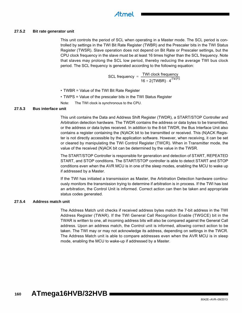
27.5.2 Bit rate generator unit
This unit controls the period of SCL when operating in a Master mode. The SCL period is con-trolled by settings in the TWI Bit Rate Register (TWBR) and the Prescaler bits in the TWI StatusRegister (TWSR). Slave operation does not depend on Bit Rate or Prescaler settings, but theCPU clock frequency in the slave must be at least 16 times higher than the SCL frequency. Notethat slaves may prolong the SCL low period, thereby reducing the average TWI bus clockperiod. The SCL frequency is generated according to the following equation:
• TWBR = Value of the TWI Bit Rate Register
• TWPS = Value of the prescaler bits in the TWI Status Register
Note: The TWI clock is synchronous to the CPU.
27.5.3 Bus interface unit
This unit contains the Data and Address Shift Register (TWDR), a START/STOP Controller andArbitration detection hardware. The TWDR contains the address or data bytes to be transmitted,or the address or data bytes received. In addition to the 8-bit TWDR, the Bus Interface Unit alsocontains a register containing the (N)ACK bit to be transmitted or received. This (N)ACK Regis-ter is not directly accessible by the application software. However, when receiving, it can be setor cleared by manipulating the TWI Control Register (TWCR). When in Transmitter mode, thevalue of the received (N)ACK bit can be determined by the value in the TWSR.
The START/STOP Controller is responsible for generation and detection of START, REPEATEDSTART, and STOP conditions. The START/STOP controller is able to detect START and STOPconditions even when the AVR MCU is in one of the sleep modes, enabling the MCU to wake upif addressed by a Master.
If the TWI has initiated a transmission as Master, the Arbitration Detection hardware continu-ously monitors the transmission trying to determine if arbitration is in process. If the TWI has lostan arbitration, the Control Unit is informed. Correct action can then be taken and appropriatestatus codes generated.
27.5.4 Address match unit
The Address Match unit checks if received address bytes match the 7-bit address in the TWIAddress Register (TWAR). If the TWI General Call Recognition Enable (TWGCE) bit in theTWAR is written to one, all incoming address bits will also be compared against the General Calladdress. Upon an address match, the Control unit is informed, allowing correct action to betaken. The TWI may or may not acknowledge its address, depending on settings in the TWCR.The Address Match unit is able to compare addresses even when the AVR MCU is in sleepmode, enabling the MCU to wake-up if addressed by a Master.
SCL frequencyTWI clock frequency
16 2(TWBR) 4TWPS+
-----------------------------------------------------------=
1608042E–AVR–09/2013
ATmega16HVB/32HVB

ATmega16HVB/32HVB
27.5.5 Control unit
The Control unit monitors the TWI bus and generates responses corresponding to settings in theTWI Control Register (TWCR). When an event requiring the attention of the application occurson the TWI bus, the TWI Interrupt Flag (TWINT) is asserted. In the next clock cycle, the TWI Sta-tus Register (TWSR) is updated with a status code identifying the event. The TWSR onlycontains relevant status information when the TWI interrupt flag is asserted. At all other times,the TWSR contains a special status code indicating that no relevant status information is avail-able. As long as the TWINT flag is set, the SCL line is held low. This allows the applicationsoftware to complete its tasks before allowing the TWI transmission to continue.
The TWINT flag is set in the following situations:
• After the TWI has transmitted a START/REPEATED START condition
• After the TWI has transmitted SLA+R/W
• After the TWI has transmitted an address byte
• After the TWI has lost arbitration
• After the TWI has been addressed by own slave address or general call
• After the TWI has received a data byte
• After a STOP or REPEATED START has been received while still addressed as a Slave
• When a bus error has occurred due to an illegal START or STOP condition
1618042E–AVR–09/2013
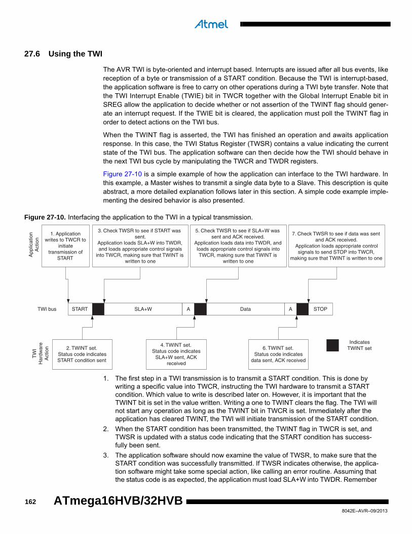
27.6 Using the TWI
The AVR TWI is byte-oriented and interrupt based. Interrupts are issued after all bus events, likereception of a byte or transmission of a START condition. Because the TWI is interrupt-based,the application software is free to carry on other operations during a TWI byte transfer. Note thatthe TWI Interrupt Enable (TWIE) bit in TWCR together with the Global Interrupt Enable bit inSREG allow the application to decide whether or not assertion of the TWINT flag should gener-ate an interrupt request. If the TWIE bit is cleared, the application must poll the TWINT flag inorder to detect actions on the TWI bus.
When the TWINT flag is asserted, the TWI has finished an operation and awaits applicationresponse. In this case, the TWI Status Register (TWSR) contains a value indicating the currentstate of the TWI bus. The application software can then decide how the TWI should behave inthe next TWI bus cycle by manipulating the TWCR and TWDR registers.
Figure 27-10 is a simple example of how the application can interface to the TWI hardware. Inthis example, a Master wishes to transmit a single data byte to a Slave. This description is quiteabstract, a more detailed explanation follows later in this section. A simple code example imple-menting the desired behavior is also presented.
Figure 27-10. Interfacing the application to the TWI in a typical transmission.
1. The first step in a TWI transmission is to transmit a START condition. This is done by writing a specific value into TWCR, instructing the TWI hardware to transmit a START condition. Which value to write is described later on. However, it is important that the TWINT bit is set in the value written. Writing a one to TWINT clears the flag. The TWI will not start any operation as long as the TWINT bit in TWCR is set. Immediately after the application has cleared TWINT, the TWI will initiate transmission of the START condition.
2. When the START condition has been transmitted, the TWINT flag in TWCR is set, and TWSR is updated with a status code indicating that the START condition has success-fully been sent.
3. The application software should now examine the value of TWSR, to make sure that the START condition was successfully transmitted. If TWSR indicates otherwise, the applica-tion software might take some special action, like calling an error routine. Assuming that the status code is as expected, the application must load SLA+W into TWDR. Remember
START SLA+W A Data A STOP
1. Applicationwrites to TWCR to
initiatetransmission of
START
2. TWINT set.Status code indicatesSTART condition sent
4. TWINT set.Status code indicates
SLA+W sent, ACKreceived
6. TWINT set.Status code indicates
data sent, ACK received
3. Check TWSR to see if START wassent.
Application loads SLA+W into TWDR,and loads appropriate control signals
into TWCR, making sure that TWINT iswritten to one
5. Check TWSR to see if SLA+W wassent and ACK received.
Application loads data into TWDR, andloads appropriate control signals intoTWCR, making sure that TWINT is
written to one
7. Check TWSR to see if data was sentand ACK received.
Application loads appropriate controlsignals to send STOP into TWCR,
making sure that TWINT is written to one
TWI bus
IndicatesTWINT set
App
licat
ion
Act
ion
TW
IH
ardw
are
Act
ion
1628042E–AVR–09/2013
ATmega16HVB/32HVB
ATmega16HVB/32HVB
that TWDR is used both for address and data. After TWDR has been loaded with the desired SLA+W, a specific value must be written to TWCR, instructing the TWI hardware to transmit the SLA+W present in TWDR. Which value to write is described later on. However, it is important that the TWINT bit is set in the value written. Writing a one to TWINT clears the flag. The TWI will not start any operation as long as the TWINT bit in TWCR is set. Immediately after the application has cleared TWINT, the TWI will initiate transmission of the address packet.
4. When the address packet has been transmitted, the TWINT flag in TWCR is set, and TWSR is updated with a status code indicating that the address packet has successfully been sent. The status code will also reflect whether a slave acknowledged the packet or not.
5. The application software should now examine the value of TWSR, to make sure that the address packet was successfully transmitted, and that the value of the ACK bit was as expected. If TWSR indicates otherwise, the application software might take some special action, like calling an error routine. Assuming that the status code is as expected, the application must load a data packet into TWDR. Subsequently, a specific value must be written to TWCR, instructing the TWI hardware to transmit the data packet present in TWDR. Which value to write is described later on. However, it is important that the TWINT bit is set in the value written. Writing a one to TWINT clears the flag. The TWI will not start any operation as long as the TWINT bit in TWCR is set. Immediately after the application has cleared TWINT, the TWI will initiate transmission of the data packet.
6. When the data packet has been transmitted, the TWINT flag in TWCR is set, and TWSR is updated with a status code indicating that the data packet has successfully been sent. The status code will also reflect whether a slave acknowledged the packet or not.
7. The application software should now examine the value of TWSR, to make sure that the data packet was successfully transmitted, and that the value of the ACK bit was as expected. If TWSR indicates otherwise, the application software might take some special action, like calling an error routine. Assuming that the status code is as expected, the application must write a specific value to TWCR, instructing the TWI hardware to transmit a STOP condition. Which value to write is described later on. However, it is important that the TWINT bit is set in the value written. Writing a one to TWINT clears the flag. The TWI will not start any operation as long as the TWINT bit in TWCR is set. Immediately after the application has cleared TWINT, the TWI will initiate transmission of the STOP condi-tion. Note that TWINT is NOT set after a STOP condition has been sent.
Even though this example is simple, it shows the principles involved in all TWI transmissions.These can be summarized as follows:
• When the TWI has finished an operation and expects application response, the TWINT flag is set. The SCL line is pulled low until TWINT is cleared
• When the TWINT flag is set, the user must update all TWI registers with the value relevant for the next TWI bus cycle. As an example, TWDR must be loaded with the value to be transmitted in the next bus cycle
• After all TWI Register updates and other pending application software tasks have been completed, TWCR is written. When writing TWCR, the TWINT bit should be set. Writing a one to TWINT clears the flag. The TWI will then commence executing whatever operation was specified by the TWCR setting
In the following an assembly and C implementation of the example is given. Note that the codebelow assumes that several definitions have been made for example by using include-files.
1638042E–AVR–09/2013

Note: 1. See ”About code examples” on page 8.
Assembly code example (1) C example (1) Comments
1
ldi r16, (1<<TWINT)|(1<<TWSTA)|
(1<<TWEN)
out TWCR, r16
TWCR = (1<<TWINT)|(1<<TWSTA)|
(1<<TWEN)Send START condition
2
wait1:
in r16,TWCR
sbrs r16,TWINT
rjmp wait1
while (!(TWCR & (1<<TWINT)))
; Wait for TWINT flag set. This indicates that the START condition has been transmitted
3
in r16,TWSR
andi r16, 0xF8
cpi r16, START
brne ERROR
if ((TWSR & 0xF8) != START)
ERROR();Check value of TWI Status Register. Mask prescaler bits. If status different from START go to ERROR
4
ldi r16, SLA_W
out TWDR, r16
ldi r16, (1<<TWINT) | (1<<TWEN)
out TWCR, r16
TWDR = SLA_W;
TWCR = (1<<TWINT) | (1<<TWEN);
Load SLA_W into TWDR Register. Clear TWINT bit in TWCR to start transmission of address
wait2:
in r16,TWCR
sbrs r16,TWINT
rjmp wait2
while (!(TWCR & (1<<TWINT)))
;Wait for TWINT flag set. This indicates that the SLA+W has been transmitted, and ACK/NACK has been received
5
in r16,TWSR
andi r16, 0xF8
cpi r16, MT_SLA_ACK
brne ERROR
if ((TWSR & 0xF8) != MT_SLA_ACK)
ERROR();
Check value of TWI Status Register. Mask prescaler bits. If status different from MT_SLA_ACK go to ERROR
ldi r16, DATA
out TWDR, r16
ldi r16, (1<<TWINT) | (1<<TWEN)
out TWCR, r16
TWDR = DATA;
TWCR = (1<<TWINT) | (1<<TWEN);
Load DATA into TWDR Register. Clear TWINT bit in TWCR to start transmission of data
6
wait3:
in r16,TWCR
sbrs r16,TWINT
rjmp wait3
while (!(TWCR & (1<<TWINT)))
;Wait for TWINT flag set. This indicates that the DATA has been transmitted, and ACK/NACK has been received
7
in r16,TWSR
andi r16, 0xF8
cpi r16, MT_DATA_ACK
brne ERROR
if ((TWSR & 0xF8) != MT_DATA_ACK)
ERROR();
Check value of TWI Status Register. Mask prescaler bits. If status different from MT_DATA_ACK go to ERROR
ldi r16, (1<<TWINT)|(1<<TWEN)|
(1<<TWSTO)
out TWCR, r16
TWCR = (1<<TWINT)|(1<<TWEN)|
(1<<TWSTO);Transmit STOP condition
1648042E–AVR–09/2013
ATmega16HVB/32HVB
ATmega16HVB/32HVB
27.7 Transmission modes
The TWI can operate in one of four major modes. These are named Master Transmitter (MT),Master Receiver (MR), Slave Transmitter (ST) and Slave Receiver (SR). Several of thesemodes can be used in the same application. As an example, the TWI can use MT mode to writedata into a TWI EEPROM, MR mode to read the data back from the EEPROM. If other mastersare present in the system, some of these might transmit data to the TWI, and then SR modewould be used. It is the application software that decides which modes are legal.
The following sections describe each of these modes. Possible status codes are describedalong with figures detailing data transmission in each of the modes. These figures contain thefollowing abbreviations:
S: START condition
Rs: REPEATED START condition
R: Read bit (high level at SDA)
W: Write bit (low level at SDA)
A: Acknowledge bit (low level at SDA)
A: Not acknowledge bit (high level at SDA)
Data: 8-bit data byte
P: STOP condition
SLA: Slave Address
In Figure 27-12 on page 168 to Figure 27-18 on page 177, circles are used to indicate that theTWINT flag is set. The numbers in the circles show the status code held in TWSR, with the pres-caler bits masked to zero. At these points, actions must be taken by the application to continueor complete the TWI transfer. The TWI transfer is suspended until the TWINT flag is cleared bysoftware.
When the TWINT flag is set, the status code in TWSR is used to determine the appropriate soft-ware action. For each status code, the required software action and details of the following serialtransfer are given in Table 27-2 on page 167 to Table 27-5 on page 176. Note that the prescalerbits are masked to zero in these tables.
27.7.1 Master Transmitter mode
In the Master Transmitter mode, a number of data bytes are transmitted to a slave receiver (seeFigure 27-11 on page 166). In order to enter a Master mode, a START condition must be trans-mitted. The format of the following address packet determines whether Master Transmitter orMaster Receiver mode is to be entered. If SLA+W is transmitted, MT mode is entered, if SLA+Ris transmitted, MR mode is entered. All the status codes mentioned in this section assume thatthe prescaler bits are zero or are masked to zero.
1658042E–AVR–09/2013
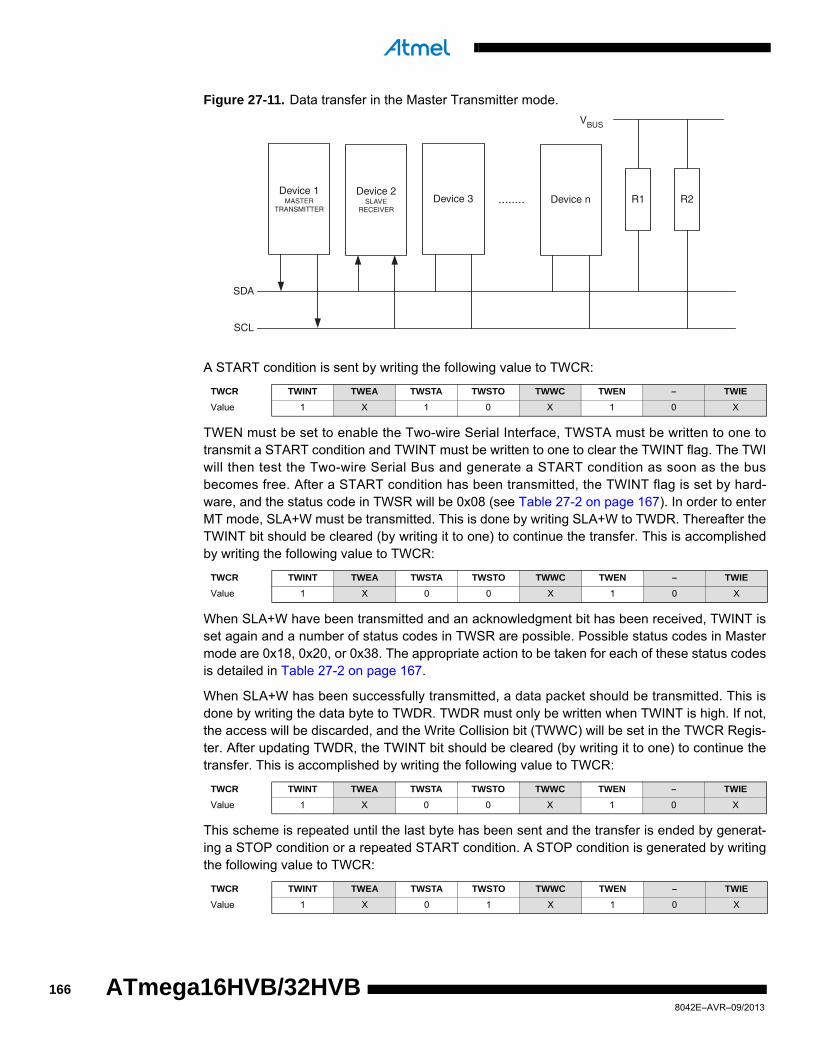
Figure 27-11. Data transfer in the Master Transmitter mode.
A START condition is sent by writing the following value to TWCR:
TWEN must be set to enable the Two-wire Serial Interface, TWSTA must be written to one totransmit a START condition and TWINT must be written to one to clear the TWINT flag. The TWIwill then test the Two-wire Serial Bus and generate a START condition as soon as the busbecomes free. After a START condition has been transmitted, the TWINT flag is set by hard-ware, and the status code in TWSR will be 0x08 (see Table 27-2 on page 167). In order to enterMT mode, SLA+W must be transmitted. This is done by writing SLA+W to TWDR. Thereafter theTWINT bit should be cleared (by writing it to one) to continue the transfer. This is accomplishedby writing the following value to TWCR:
When SLA+W have been transmitted and an acknowledgment bit has been received, TWINT isset again and a number of status codes in TWSR are possible. Possible status codes in Mastermode are 0x18, 0x20, or 0x38. The appropriate action to be taken for each of these status codesis detailed in Table 27-2 on page 167.
When SLA+W has been successfully transmitted, a data packet should be transmitted. This isdone by writing the data byte to TWDR. TWDR must only be written when TWINT is high. If not,the access will be discarded, and the Write Collision bit (TWWC) will be set in the TWCR Regis-ter. After updating TWDR, the TWINT bit should be cleared (by writing it to one) to continue thetransfer. This is accomplished by writing the following value to TWCR:
This scheme is repeated until the last byte has been sent and the transfer is ended by generat-ing a STOP condition or a repeated START condition. A STOP condition is generated by writingthe following value to TWCR:
TWCR TWINT TWEA TWSTA TWSTO TWWC TWEN – TWIE
Value 1 X 1 0 X 1 0 X
TWCR TWINT TWEA TWSTA TWSTO TWWC TWEN – TWIE
Value 1 X 0 0 X 1 0 X
TWCR TWINT TWEA TWSTA TWSTO TWWC TWEN – TWIE
Value 1 X 0 0 X 1 0 X
TWCR TWINT TWEA TWSTA TWSTO TWWC TWEN – TWIE
Value 1 X 0 1 X 1 0 X
Device 1MASTER
TRANSMITTER
Device 2SLAVE
RECEIVERDevice 3 Device n
SDA
SCL
........ R1 R2
VBUS
1668042E–AVR–09/2013
ATmega16HVB/32HVB

ATmega16HVB/32HVB
A REPEATED START condition is generated by writing the following value to TWCR:
After a repeated START condition (state 0x10) the Two-wire Serial Interface can access thesame slave again, or a new slave without transmitting a STOP condition. Repeated STARTenables the master to switch between slaves, Master Transmitter mode and Master Receivermode without losing control of the bus.
TWCR TWINT TWEA TWSTA TWSTO TWWC TWEN – TWIE
Value 1 X 1 0 X 1 0 X
Table 27-2. Status codes for Master Transmitter mode.
Status code(TWSR)prescaler bitsare 0
Status of the two-wire serialbus and two-wire serial inter-face hardware
Application software response
Next action taken by TWI hardwareTo/from TWDR
To TWCR
STA STO TWINT TWEA
0x08 A START condition has beentransmitted
Load SLA+W X 0 1 X SLA+W will be transmitted;ACK or NOT ACK will be received
0x10 A repeated START conditionhas been transmitted
Load SLA+W or
Load SLA+R
X
X
0
0
1
1
X
X
SLA+W will be transmitted;ACK or NOT ACK will be receivedSLA+R will be transmitted;Logic will switch to Master Receiver mode
0x18 SLA+W has been transmitted;ACK has been received
Load data byte or
No TWDR action orNo TWDR action or
No TWDR action
0
10
1
0
01
1
1
11
1
X
XX
X
Data byte will be transmitted and ACK or NOT ACK will be receivedRepeated START will be transmittedSTOP condition will be transmitted andTWSTO flag will be resetSTOP condition followed by a START condition will be transmitted and TWSTO flag will be reset
0x20 SLA+W has been transmitted;NOT ACK has been received
Load data byte or
No TWDR action orNo TWDR action or
No TWDR action
0
10
1
0
01
1
1
11
1
X
XX
X
Data byte will be transmitted and ACK or NOT ACK will be receivedRepeated START will be transmittedSTOP condition will be transmitted andTWSTO flag will be resetSTOP condition followed by a START condition will be transmitted and TWSTO flag will be reset
0x28 Data byte has been transmit-ted;ACK has been received
Load data byte or
No TWDR action orNo TWDR action or
No TWDR action
0
10
1
0
01
1
1
11
1
X
XX
X
Data byte will be transmitted and ACK or NOT ACK will be receivedRepeated START will be transmittedSTOP condition will be transmitted andTWSTO flag will be resetSTOP condition followed by a START condition will be transmitted and TWSTO flag will be reset
0x30 Data byte has been transmit-ted;NOT ACK has been received
Load data byte or
No TWDR action orNo TWDR action or
No TWDR action
0
10
1
0
01
1
1
11
1
X
XX
X
Data byte will be transmitted and ACK or NOT ACK will be receivedRepeated START will be transmittedSTOP condition will be transmitted andTWSTO flag will be resetSTOP condition followed by a START condition will be transmitted and TWSTO flag will be reset
0x38 Arbitration lost in SLA+W ordata bytes
No TWDR action or
No TWDR action
0
1
0
0
1
1
X
X
Two-wire Serial Bus will be released and not ad-dressed slave mode enteredA START condition will be transmitted when the bus becomes free
1678042E–AVR–09/2013
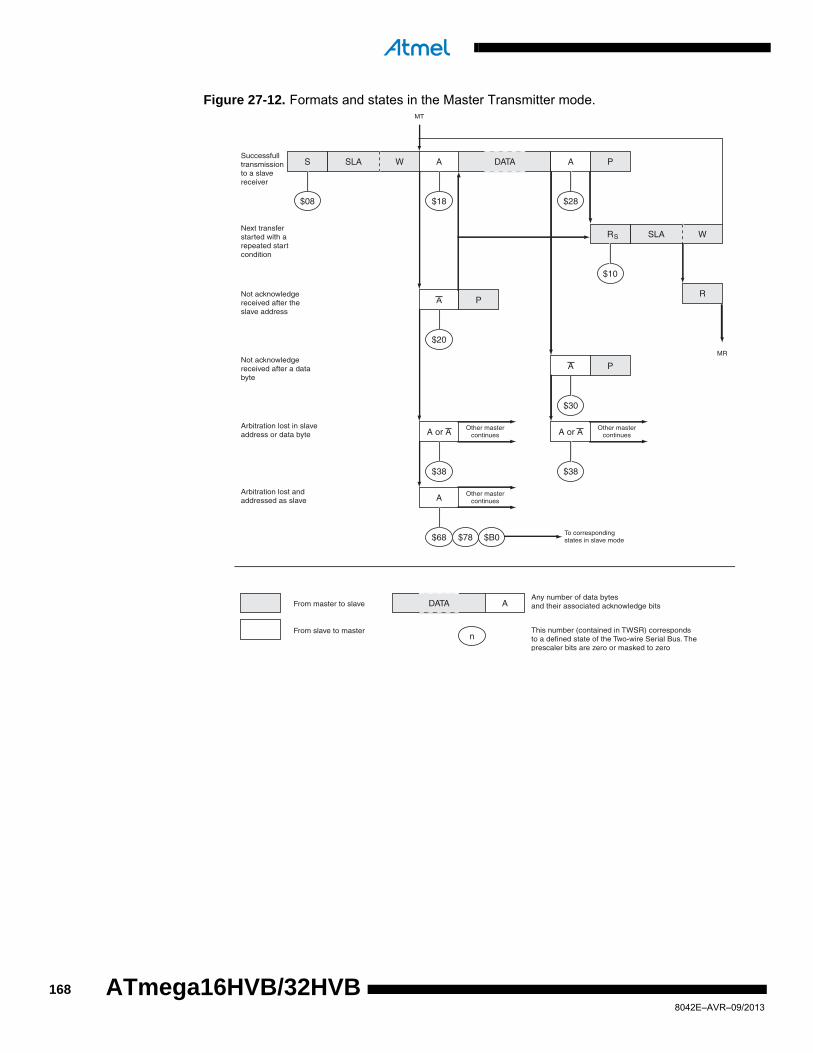
Figure 27-12. Formats and states in the Master Transmitter mode.
S SLA W A DATA A P
$08 $18 $28
R SLA W
$10
A P
$20
P
$30
A or A
$38
A
Other mastercontinues A or A
$38
Other mastercontinues
R
A
$68
Other mastercontinues
$78 $B0To correspondingstates in slave mode
MT
MR
Successfulltransmissionto a slavereceiver
Next transferstarted with arepeated startcondition
Not acknowledgereceived after theslave address
Not acknowledgereceived after a databyte
Arbitration lost in slaveaddress or data byte
Arbitration lost andaddressed as slave
DATA A
n
From master to slave
From slave to master
Any number of data bytesand their associated acknowledge bits
This number (contained in TWSR) correspondsto a defined state of the Two-wire Serial Bus. Theprescaler bits are zero or masked to zero
S
1688042E–AVR–09/2013
ATmega16HVB/32HVB

ATmega16HVB/32HVB
27.7.2 Master Receiver mode
In the Master Receiver mode, a number of data bytes are received from a slave transmitter (seeFigure 27-13). In order to enter a Master mode, a START condition must be transmitted. The for-mat of the following address packet determines whether Master Transmitter or Master Receivermode is to be entered. If SLA+W is transmitted, MT mode is entered, if SLA+R is transmitted,MR mode is entered. All the status codes mentioned in this section assume that the prescalerbits are zero or are masked to zero.
Figure 27-13. Data transfer in Master Receiver mode.
A START condition is sent by writing the following value to TWCR:
TWEN must be written to one to enable the Two-wire Serial Interface, TWSTA must be written toone to transmit a START condition and TWINT must be set to clear the TWINT flag. The TWI willthen test the Two-wire Serial Bus and generate a START condition as soon as the bus becomesfree. After a START condition has been transmitted, the TWINT flag is set by hardware, and thestatus code in TWSR will be 0x08 (see Table 27-2 on page 167). In order to enter MR mode,SLA+R must be transmitted. This is done by writing SLA+R to TWDR. Thereafter the TWINT bitshould be cleared (by writing it to one) to continue the transfer. This is accomplished by writingthe following value to TWCR:
When SLA+R have been transmitted and an acknowledgment bit has been received, TWINT isset again and a number of status codes in TWSR are possible. Possible status codes in Mastermode are 0x38, 0x40, or 0x48. The appropriate action to be taken for each of these status codesis detailed in Table 27-12 on page 168. Received data can be read from the TWDR Registerwhen the TWINT flag is set high by hardware. This scheme is repeated until the last byte hasbeen received. After the last byte has been received, the MR should inform the ST by sending aNACK after the last received data byte. The transfer is ended by generating a STOP condition ora repeated START condition.
TWCR TWINT TWEA TWSTA TWSTO TWWC TWEN – TWIE
Value 1 X 1 0 X 1 0 X
TWCR TWINT TWEA TWSTA TWSTO TWWC TWEN – TWIE
Value 1 X 0 0 X 1 0 X
Device 1MASTER
RECEIVER
Device 2SLAVE
TRANSMITTERDevice 3 Device n
SDA
SCL
........ R1 R2
VBUS
1698042E–AVR–09/2013
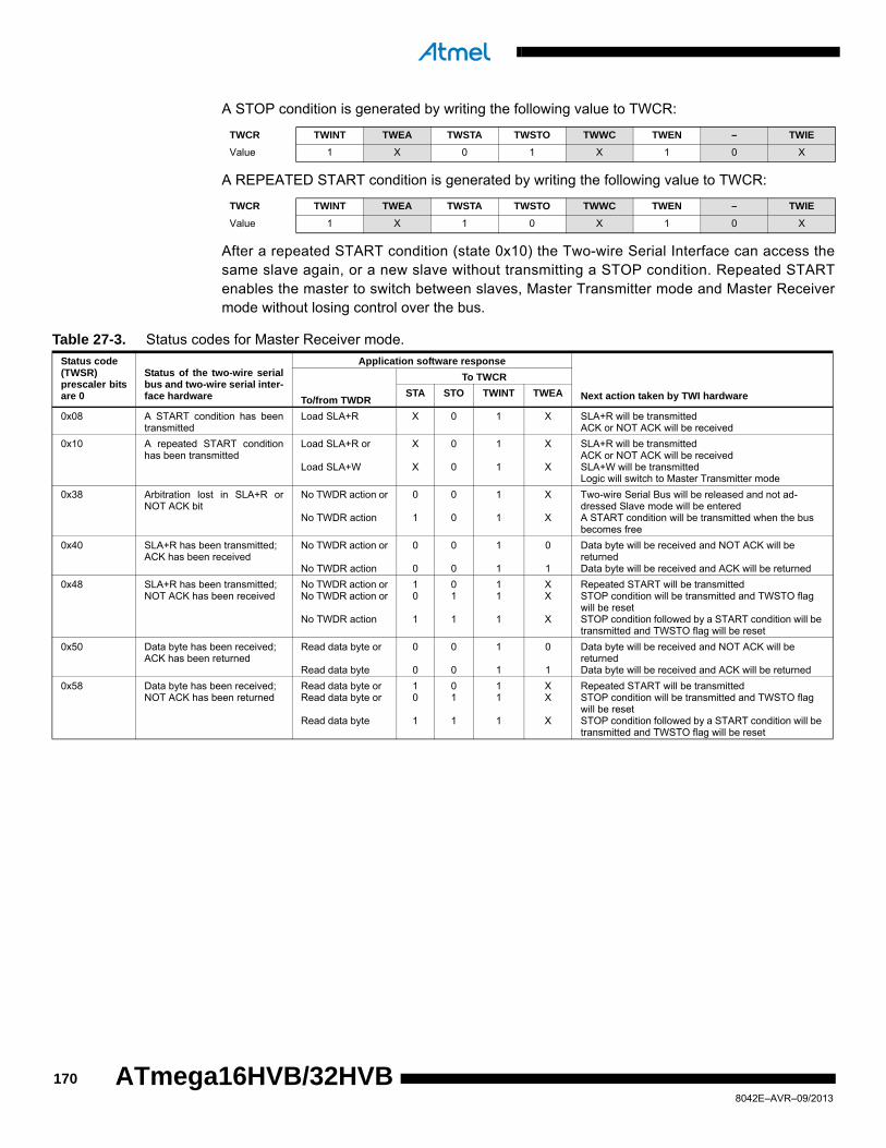
A STOP condition is generated by writing the following value to TWCR:
A REPEATED START condition is generated by writing the following value to TWCR:
After a repeated START condition (state 0x10) the Two-wire Serial Interface can access thesame slave again, or a new slave without transmitting a STOP condition. Repeated STARTenables the master to switch between slaves, Master Transmitter mode and Master Receivermode without losing control over the bus.
TWCR TWINT TWEA TWSTA TWSTO TWWC TWEN – TWIE
Value 1 X 0 1 X 1 0 X
TWCR TWINT TWEA TWSTA TWSTO TWWC TWEN – TWIE
Value 1 X 1 0 X 1 0 X
Table 27-3. Status codes for Master Receiver mode.
Status code(TWSR)prescaler bitsare 0
Status of the two-wire serialbus and two-wire serial inter-face hardware
Application software response
Next action taken by TWI hardwareTo/from TWDR
To TWCR
STA STO TWINT TWEA
0x08 A START condition has beentransmitted
Load SLA+R X 0 1 X SLA+R will be transmittedACK or NOT ACK will be received
0x10 A repeated START conditionhas been transmitted
Load SLA+R or
Load SLA+W
X
X
0
0
1
1
X
X
SLA+R will be transmittedACK or NOT ACK will be receivedSLA+W will be transmittedLogic will switch to Master Transmitter mode
0x38 Arbitration lost in SLA+R orNOT ACK bit
No TWDR action or
No TWDR action
0
1
0
0
1
1
X
X
Two-wire Serial Bus will be released and not ad-dressed Slave mode will be enteredA START condition will be transmitted when the busbecomes free
0x40 SLA+R has been transmitted;ACK has been received
No TWDR action or
No TWDR action
0
0
0
0
1
1
0
1
Data byte will be received and NOT ACK will be returnedData byte will be received and ACK will be returned
0x48 SLA+R has been transmitted;NOT ACK has been received
No TWDR action orNo TWDR action or
No TWDR action
10
1
01
1
11
1
XX
X
Repeated START will be transmittedSTOP condition will be transmitted and TWSTO flag will be resetSTOP condition followed by a START condition will be transmitted and TWSTO flag will be reset
0x50 Data byte has been received;ACK has been returned
Read data byte or
Read data byte
0
0
0
0
1
1
0
1
Data byte will be received and NOT ACK will be returnedData byte will be received and ACK will be returned
0x58 Data byte has been received;NOT ACK has been returned
Read data byte orRead data byte or
Read data byte
10
1
01
1
11
1
XX
X
Repeated START will be transmittedSTOP condition will be transmitted and TWSTO flag will be resetSTOP condition followed by a START condition will be transmitted and TWSTO flag will be reset
1708042E–AVR–09/2013
ATmega16HVB/32HVB
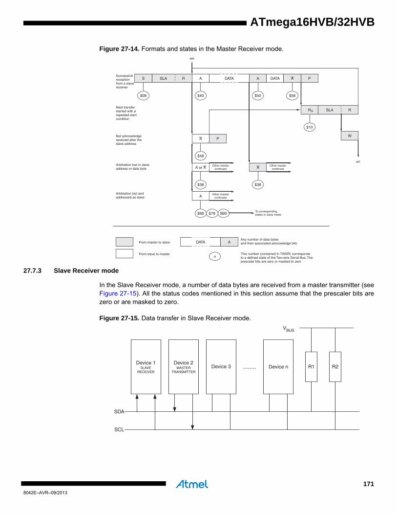
ATmega16HVB/32HVB
Figure 27-14. Formats and states in the Master Receiver mode.
27.7.3 Slave Receiver mode
In the Slave Receiver mode, a number of data bytes are received from a master transmitter (seeFigure 27-15). All the status codes mentioned in this section assume that the prescaler bits arezero or are masked to zero.
Figure 27-15. Data transfer in Slave Receiver mode.
S SLA R A DATA A
$08 $40 $50
SLA R
$10
A P
$48
A or A
$38
Other mastercontinues
$38
Other mastercontinues
W
A
$68
Other mastercontinues
$78 $B0To correspondingstates in slave mode
MR
MT
Successfullreceptionfrom a slavereceiver
Next transferstarted with arepeated startcondition
Not acknowledgereceived after theslave address
Arbitration lost in slaveaddress or data byte
Arbitration lost andaddressed as slave
DATA A
n
From master to slave
From slave to master
Any number of data bytesand their associated acknowledge bits
This number (contained in TWSR) correspondsto a defined state of the Two-wire Serial Bus. The prescaler bits are zero or masked to zero
PDATA A
$58
A
RS
Device 3 Device n
SDA
SCL
........ R1 R2
VBUS
Device 2MASTER
TRANSMITTER
Device 1SLAVE
RECEIVER
1718042E–AVR–09/2013

To initiate the Slave Receiver mode, TWAR and TWCR must be initialized as follows:
The upper seven bits are the address to which the Two-wire Serial Interface will respond whenaddressed by a master. If the LSB is set, the TWI will respond to the general call address (0x00),otherwise it will ignore the general call address.
TWEN must be written to one to enable the TWI. The TWEA bit must be written to one to enablethe acknowledgment of the device’s own slave address or the general call address. TWSTA andTWSTO must be written to zero.
When TWAR and TWCR have been initialized, the TWI waits until it is addressed by its ownslave address (or the general call address if enabled) followed by the data direction bit. If thedirection bit is “0” (write), the TWI will operate in SR mode, otherwise ST mode is entered. Afterits own slave address and the write bit have been received, the TWINT flag is set and a validstatus code can be read from TWSR. The status code is used to determine the appropriate soft-ware action. The appropriate action to be taken for each status code is detailed in Table 27-4 onpage 173. The Slave Receiver mode may also be entered if arbitration is lost while the TWI is inthe Master mode (see states 0x68 and 0x78).
If the TWEA bit is reset during a transfer, the TWI will return a “Not Acknowledge” (“1”) to SDAafter the next received data byte. This can be used to indicate that the slave is not able toreceive any more bytes. While TWEA is zero, the TWI does not acknowledge its own slaveaddress. However, the Two-wire Serial Bus is still monitored and address recognition mayresume at any time by setting TWEA. This implies that the TWEA bit may be used to temporarilyisolate the TWI from the Two-wire Serial Bus.
In all sleep modes other than Idle mode, the clock system to the TWI is turned off. If the TWEAbit is set, the interface can still acknowledge its own slave address or the general call address byusing the Two-wire Serial Bus clock as a clock source. The part will then wake-up from sleepand the TWI will hold the SCL clock low during the wake up and until the TWINT flag is cleared(by writing it to one). Further data reception will be carried out as normal, with the AVR clocksrunning as normal. Observe that if the AVR is set up with a long start-up time, the SCL line maybe held low for a long time, blocking other data transmissions.
Note that the Two-wire Serial Interface Data Register – TWDR does not reflect the last bytepresent on the bus when waking up from these Sleep modes.
TWAR TWA6 TWA5 TWA4 TWA3 TWA2 TWA1 TWA0 TWGCE
Value Device’s Own Slave Address
TWCR TWINT TWEA TWSTA TWSTO TWWC TWEN – TWIE
Value 0 1 0 0 0 1 0 X
1728042E–AVR–09/2013
ATmega16HVB/32HVB

ATmega16HVB/32HVB
Table 27-4. Status codes for Slave Receiver mode.
Status code(TWSR)prescaler bitsare 0
Status of the two-wire serialbus and two-wire serial inter-face hardware
Application software response
Next action taken by TWI hardwareTo/from TWDR
To TWCR
STA STO TWINT TWEA
0x60 Own SLA+W has been received;ACK has been returned
No TWDR action or
No TWDR action
X
X
0
0
1
1
0
1
Data byte will be received and NOT ACK will bereturnedData byte will be received and ACK will be returned
0x68 Arbitration lost in SLA+R/W asmaster; own SLA+W has beenreceived; ACK has been returned
No TWDR action or
No TWDR action
X
X
0
0
1
1
0
1
Data byte will be received and NOT ACK will bereturnedData byte will be received and ACK will be returned
0x70 General call address has beenreceived; ACK has been returned
No TWDR action or
No TWDR action
X
X
0
0
1
1
0
1
Data byte will be received and NOT ACK will bereturnedData byte will be received and ACK will be returned
0x78 Arbitration lost in SLA+R/W asmaster; General call address hasbeen received; ACK has beenreturned
No TWDR action or
No TWDR action
X
X
0
0
1
1
0
1
Data byte will be received and NOT ACK will bereturnedData byte will be received and ACK will be returned
0x80 Previously addressed with ownSLA+W; data has been received;ACK has been returned
Read data byte or
Read data byte
X
X
0
0
1
1
0
1
Data byte will be received and NOT ACK will bereturnedData byte will be received and ACK will be returned
0x88 Previously addressed with ownSLA+W; data has been received;NOT ACK has been returned
Read data byte or
Read data byte or
Read data byte or
Read data byte
0
0
1
1
0
0
0
0
1
1
1
1
0
1
0
1
Switched to the not addressed Slave mode;no recognition of own SLA or GCASwitched to the not addressed Slave mode;own SLA will be recognized;GCA will be recognized if TWGCE = “1”Switched to the not addressed Slave mode;no recognition of own SLA or GCA;a START condition will be transmitted when the busbecomes freeSwitched to the not addressed Slave mode;own SLA will be recognized;GCA will be recognized if TWGCE = “1”;a START condition will be transmitted when the busbecomes free
0x90 Previously addressed withgeneral call; data has been re-ceived; ACK has been returned
Read data byte or
Read data byte
X
X
0
0
1
1
0
1
Data byte will be received and NOT ACK will bereturnedData byte will be received and ACK will be returned
0x98 Previously addressed withgeneral call; data has beenreceived; NOT ACK has beenreturned
Read data byte or
Read data byte or
Read data byte or
Read data byte
0
0
1
1
0
0
0
0
1
1
1
1
0
1
0
1
Switched to the not addressed Slave mode;no recognition of own SLA or GCASwitched to the not addressed Slave mode;own SLA will be recognized;GCA will be recognized if TWGCE = “1”Switched to the not addressed Slave mode;no recognition of own SLA or GCA;a START condition will be transmitted when the busbecomes freeSwitched to the not addressed Slave mode;own SLA will be recognized;GCA will be recognized if TWGCE = “1”;a START condition will be transmitted when the busbecomes free
0xA0 A STOP condition or repeatedSTART condition has beenreceived while still addressed asslave
Read data byte or
Read data byte or
Read data byte or
Read data byte
0
0
1
1
0
0
0
0
1
1
1
1
0
1
0
1
Switched to the not addressed Slave mode;no recognition of own SLA or GCASwitched to the not addressed Slave mode;own SLA will be recognized;GCA will be recognized if TWGCE = “1”Switched to the not addressed Slave mode;no recognition of own SLA or GCA;a START condition will be transmitted when the busbecomes freeSwitched to the not addressed Slave mode;own SLA will be recognized;GCA will be recognized if TWGCE = “1”;a START condition will be transmitted when the busbecomes free
1738042E–AVR–09/2013

Figure 27-16. Formats and states in the Slave Receiver mode.
S SLA W A DATA A
$60 $80
$88
A
$68
Reception of the ownslave address and one ormore data bytes. All areacknowledged
Last data byte receivedis not acknowledged
Arbitration lost as masterand addressed as slave
Reception of the general calladdress and one or more databytes
Last data byte received isnot acknowledged
n
From master to slave
From slave to master
Any number of data bytesand their associated acknowledge bits
This number (contained in TWSR) correspondsto a defined state of the Two-wire Serial Bus. The prescaler bits are zero or masked to zero
P or SDATA A
$80 $A0
P or SA
A DATA A
$70 $90
$98
A
$78
P or SDATA A
$90 $A0
P or SA
General Call
Arbitration lost as master andaddressed as slave by general call
DATA A
1748042E–AVR–09/2013
ATmega16HVB/32HVB
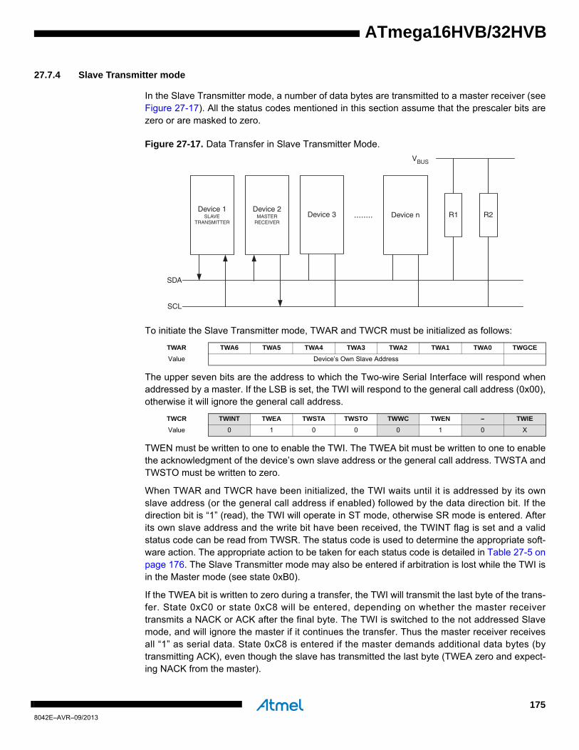
ATmega16HVB/32HVB
27.7.4 Slave Transmitter mode
In the Slave Transmitter mode, a number of data bytes are transmitted to a master receiver (seeFigure 27-17). All the status codes mentioned in this section assume that the prescaler bits arezero or are masked to zero.
Figure 27-17. Data Transfer in Slave Transmitter Mode.
To initiate the Slave Transmitter mode, TWAR and TWCR must be initialized as follows:
The upper seven bits are the address to which the Two-wire Serial Interface will respond whenaddressed by a master. If the LSB is set, the TWI will respond to the general call address (0x00),otherwise it will ignore the general call address.
TWEN must be written to one to enable the TWI. The TWEA bit must be written to one to enablethe acknowledgment of the device’s own slave address or the general call address. TWSTA andTWSTO must be written to zero.
When TWAR and TWCR have been initialized, the TWI waits until it is addressed by its ownslave address (or the general call address if enabled) followed by the data direction bit. If thedirection bit is “1” (read), the TWI will operate in ST mode, otherwise SR mode is entered. Afterits own slave address and the write bit have been received, the TWINT flag is set and a validstatus code can be read from TWSR. The status code is used to determine the appropriate soft-ware action. The appropriate action to be taken for each status code is detailed in Table 27-5 onpage 176. The Slave Transmitter mode may also be entered if arbitration is lost while the TWI isin the Master mode (see state 0xB0).
If the TWEA bit is written to zero during a transfer, the TWI will transmit the last byte of the trans-fer. State 0xC0 or state 0xC8 will be entered, depending on whether the master receivertransmits a NACK or ACK after the final byte. The TWI is switched to the not addressed Slavemode, and will ignore the master if it continues the transfer. Thus the master receiver receivesall “1” as serial data. State 0xC8 is entered if the master demands additional data bytes (bytransmitting ACK), even though the slave has transmitted the last byte (TWEA zero and expect-ing NACK from the master).
TWAR TWA6 TWA5 TWA4 TWA3 TWA2 TWA1 TWA0 TWGCE
Value Device’s Own Slave Address
TWCR TWINT TWEA TWSTA TWSTO TWWC TWEN – TWIE
Value 0 1 0 0 0 1 0 X
Device 3 Device n
SDA
SCL
........ R1 R2
VBUS
Device 2MASTER
RECEIVER
Device 1SLAVE
TRANSMITTER
1758042E–AVR–09/2013

While TWEA is zero, the TWI does not respond to its own slave address. However, the Two-wireSerial Bus is still monitored and address recognition may resume at any time by setting TWEA.This implies that the TWEA bit may be used to temporarily isolate the TWI from the Two-wireSerial Bus.
In all sleep modes other than Idle mode, the clock system to the TWI is turned off. If the TWEAbit is set, the interface can still acknowledge its own slave address or the general call address byusing the Two-wire Serial Bus clock as a clock source. The part will then wake up from sleepand the TWI will hold the SCL clock will low during the wake up and until the TWINT flag iscleared (by writing it to one). Further data transmission will be carried out as normal, with theAVR clocks running as normal. Observe that if the AVR is set up with a long start-up time, theSCL line may be held low for a long time, blocking other data transmissions.
Note that the Two-wire Serial Interface Data Register – TWDR – does not reflect the last bytepresent on the bus when waking up from these sleep modes.
Table 27-5. Status codes for Slave Transmitter mode.
Status code(TWSR)prescalerbits are 0
Status of the two-wire serialbus and two-wire serial inter-face hardware
Application software response
Next action taken by TWI hardwareTo/from TWDR
To TWCR
STA STO TWINT TWEA
0xA8 Own SLA+R has been received;ACK has been returned
Load data byte or
Load data byte
X
X
0
0
1
1
0
1
Last data byte will be transmitted and NOT ACK should be receivedData byte will be transmitted and ACK should be re-ceived
0xB0 Arbitration lost in SLA+R/W asmaster; own SLA+R has beenreceived; ACK has been returned
Load data byte or
Load data byte
X
X
0
0
1
1
0
1
Last data byte will be transmitted and NOT ACK should be receivedData byte will be transmitted and ACK should be re-ceived
0xB8 Data byte in TWDR has beentransmitted; ACK has beenreceived
Load data byte or
Load data byte
X
X
0
0
1
1
0
1
Last data byte will be transmitted and NOT ACK should be receivedData byte will be transmitted and ACK should be re-ceived
0xC0 Data byte in TWDR has beentransmitted; NOT ACK has beenreceived
No TWDR action or
No TWDR action or
No TWDR action or
No TWDR action
0
0
1
1
0
0
0
0
1
1
1
1
0
1
0
1
Switched to the not addressed Slave mode;no recognition of own SLA or GCASwitched to the not addressed Slave mode;own SLA will be recognized;GCA will be recognized if TWGCE = “1”Switched to the not addressed Slave mode;no recognition of own SLA or GCA;a START condition will be transmitted when the busbecomes freeSwitched to the not addressed Slave mode;own SLA will be recognized;GCA will be recognized if TWGCE = “1”;a START condition will be transmitted when the busbecomes free
0xC8 Last data byte in TWDR has beentransmitted (TWEA = “0”); ACKhas been received
No TWDR action or
No TWDR action or
No TWDR action or
No TWDR action
0
0
1
1
0
0
0
0
1
1
1
1
0
1
0
1
Switched to the not addressed Slave mode;no recognition of own SLA or GCASwitched to the not addressed Slave mode;own SLA will be recognized;GCA will be recognized if TWGCE = “1”Switched to the not addressed Slave mode;no recognition of own SLA or GCA;a START condition will be transmitted when the busbecomes freeSwitched to the not addressed Slave mode;own SLA will be recognized;GCA will be recognized if TWGCE = “1”;a START condition will be transmitted when the busbecomes free
1768042E–AVR–09/2013
ATmega16HVB/32HVB
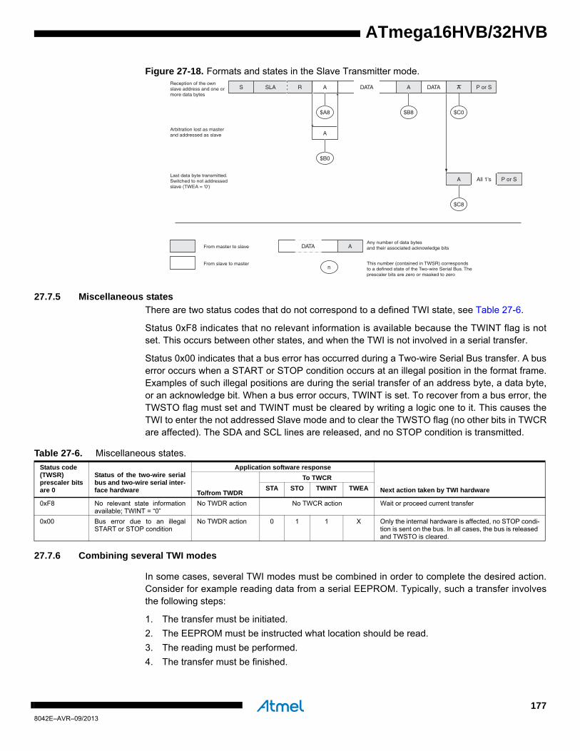
ATmega16HVB/32HVB
Figure 27-18. Formats and states in the Slave Transmitter mode.
27.7.5 Miscellaneous states
There are two status codes that do not correspond to a defined TWI state, see Table 27-6.
Status 0xF8 indicates that no relevant information is available because the TWINT flag is notset. This occurs between other states, and when the TWI is not involved in a serial transfer.
Status 0x00 indicates that a bus error has occurred during a Two-wire Serial Bus transfer. A buserror occurs when a START or STOP condition occurs at an illegal position in the format frame.Examples of such illegal positions are during the serial transfer of an address byte, a data byte,or an acknowledge bit. When a bus error occurs, TWINT is set. To recover from a bus error, theTWSTO flag must set and TWINT must be cleared by writing a logic one to it. This causes theTWI to enter the not addressed Slave mode and to clear the TWSTO flag (no other bits in TWCRare affected). The SDA and SCL lines are released, and no STOP condition is transmitted.
27.7.6 Combining several TWI modes
In some cases, several TWI modes must be combined in order to complete the desired action.Consider for example reading data from a serial EEPROM. Typically, such a transfer involvesthe following steps:
1. The transfer must be initiated.
2. The EEPROM must be instructed what location should be read.
3. The reading must be performed.
4. The transfer must be finished.
S SLA R A DATA A
$A8 $B8
A
$B0
Reception of the ownslave address and one ormore data bytes
Last data byte transmitted.Switched to not addressedslave (TWEA = '0')
Arbitration lost as masterand addressed as slave
n
From master to slave
From slave to master
Any number of data bytesand their associated acknowledge bits
This number (contained in TWSR) correspondsto a defined state of the Two-wire Serial Bus. The prescaler bits are zero or masked to zero
P or SDATA
$C0
DATA A
A
$C8
P or SAll 1's
A
Table 27-6. Miscellaneous states.
Status code(TWSR)prescaler bitsare 0
Status of the two-wire serialbus and two-wire serial inter-face hardware
Application software response
Next action taken by TWI hardwareTo/from TWDR
To TWCR
STA STO TWINT TWEA
0xF8 No relevant state informationavailable; TWINT = “0”
No TWDR action No TWCR action Wait or proceed current transfer
0x00 Bus error due to an illegalSTART or STOP condition
No TWDR action 0 1 1 X Only the internal hardware is affected, no STOP condi-tion is sent on the bus. In all cases, the bus is released and TWSTO is cleared.
1778042E–AVR–09/2013

Note that data is transmitted both from Master to Slave and vice versa. The Master must instructthe slave what location it wants to read, requiring the use of the MT mode. Subsequently, datamust be read from the slave, implying the use of the MR mode. Thus, the transfer direction mustbe changed. The Master must keep control of the bus during all these steps, and the stepsshould be carried out as an atomic operation. If this principle is violated in a multi-master sys-tem, another master can alter the data pointer in the EEPROM between steps 2 and 3, and themaster will read the wrong data location. Such a change in transfer direction is accomplished bytransmitting a REPEATED START between the transmission of the address byte and receptionof the data. After a REPEATED START, the master keeps ownership of the bus. The followingfigure shows the flow in this transfer.
Figure 27-19. Combining Several TWI Modes to Access a Serial EEPROM.
27.8 Multi-master systems and arbitration
If multiple masters are connected to the same bus, transmissions may be initiated simultane-ously by one or more of them. The TWI standard ensures that such situations are handled insuch a way that one of the masters will be allowed to proceed with the transfer, and that no datawill be lost in the process. An example of an arbitration situation is depicted below, where twomasters are trying to transmit data to a slave receiver.
Figure 27-20. An arbitration example.
Several different scenarios may arise during arbitration, as described below:
• Two or more masters are performing identical communication with the same slave. In this case, neither the slave nor any of the masters will know about the bus contention
• Two or more masters are accessing the same slave with different data or direction bit. In this case, arbitration will occur, either in the READ/WRITE bit or in the data bits. The masters trying
Master Transmitter Master Receiver
S = START Rs = REPEATED START P = STOP
Transmitted from master to slave Transmitted from slave to master
S SLA+W A ADDRESS A Rs SLA+R A DATA A P
Device 1MASTER
TRANSMITTER
Device 2MASTER
TRANSMITTER
Device 3SLAVE
RECEIVERDevice n
SDA
SCL
........ R1 R2
VBUS
1788042E–AVR–09/2013
ATmega16HVB/32HVB

ATmega16HVB/32HVB
to output a one on SDA while another master outputs a zero will lose the arbitration. Losing masters will switch to not addressed Slave mode or wait until the bus is free and transmit a new START condition, depending on application software action
• Two or more masters are accessing different slaves. In this case, arbitration will occur in the SLA bits. Masters trying to output a one on SDA while another master outputs a zero will lose the arbitration. Masters losing arbitration in SLA will switch to Slave mode to check if they are being addressed by the winning master. If addressed, they will switch to SR or ST mode, depending on the value of the READ/WRITE bit. If they are not being addressed, they will switch to not addressed Slave mode or wait until the bus is free and transmit a new START condition, depending on application software action
This is summarized in Figure 27-21. Possible status values are given in circles.
Figure 27-21. Possible status codes caused by arbitration.
27.9 Bus connect/disconnect for two-wire serial interface
The Bus Connect/Disconnect module is an addition to the TWI Interface. Based on a configura-tion bit, an interrupt can be generated either when the TWI bus is connected or disconnected.
Figure 27-22 on page 180 illustrates the Bus Connect/Disconnect logic, where SDA and SCLare the TWI data and clock lines, respectively.
When the TWI bus is connected, both the SDA and the SCL lines will become high simultane-ously. If the TWBCIP bit is cleared, the interrupt will be executed if enabled. Once the bus isconnected, the TWBCIP bit should be set. This enables detection of when the bus is discon-nected, and prevents repetitive interrupts every time both the SDA and SCL lines are high (forexample bus IDLE state).
When the TWI bus is disconnected, both the SDA and the SCL lines will become low simultane-ously. If the TWBCIP bit is set, the interrupt will be executed if enabled and if both lines remainlow for a configurable time period. By adding this time constraint, unwanted interrupts caused byboth lines going low during normal bus communication is prevented. Once the bus is discon-nected, the TWBCIP bit should be cleared. This enables detection of when the bus is connected,and prevents repetitive interrupts if the SCL and SDA lines remain low.
OwnAddress / General Call
received
Arbitration lost in SLA
TWI bus will be released and not addressed slave mode will be enteredA START condition will be transmitted when the bus becomes free
No
Arbitration lost in Data
Direction
Yes
Write Data byte will be received and NOT ACK will be returnedData byte will be received and ACK will be returned
Last data byte will be transmitted and NOT ACK should be receivedData byte will be transmitted and ACK should be received
ReadB0
68/78
38
SLASTART Data STOP
1798042E–AVR–09/2013
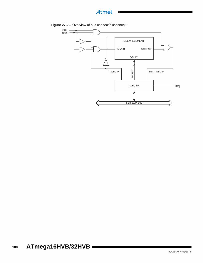
Figure 27-22. Overview of bus connect/disconnect.
DELAY ELEMENT
START OUTPUT
DELAY
TWBCSR
SDASCL
SET TWBCIF
IRQ
TW
BD
T
TWBCIP
8-BIT DATA BUS
1808042E–AVR–09/2013
ATmega16HVB/32HVB

ATmega16HVB/32HVB
27.10 Register description
27.10.1 TWBR – TWI Bit Rate Register
• Bits 7:0 – TWI Bit Rate Register
TWBR selects the division factor for the bit rate generator. The bit rate generator is a frequencydivider which generates the SCL clock frequency in the Master modes. See ”Bit rate generatorunit” on page 160 for calculating bit rates.
27.10.2 TWCR – TWI Control Register
The TWCR is used to control the operation of the TWI. It is used to enable the TWI, to initiate aMaster access by applying a START condition to the bus, to generate a Receiver acknowledge,to generate a stop condition, and to control halting of the bus while the data to be written to thebus are written to the TWDR. It also indicates a write collision if data is attempted written toTWDR while the register is inaccessible.
• Bit 7 – TWINT: TWI Interrupt Flag
This bit is set by hardware when the TWI has finished its current job and expects applicationsoftware response. If the I-bit in SREG and TWIE in TWCR are set, the MCU will jump to theTWI Interrupt Vector. While the TWINT flag is set, the SCL low period is stretched. The TWINTflag must be cleared by software by writing a logic one to it. Note that this flag is not automati-cally cleared by hardware when executing the interrupt routine. Also note that clearing this flagstarts the operation of the TWI, so all accesses to the TWI Address Register (TWAR), TWI Sta-tus Register (TWSR), and TWI Data Register (TWDR) must be complete before clearing thisflag.
• Bit 6 – TWEA: TWI Enable Acknowledge Bit
The TWEA bit controls the generation of the acknowledge pulse. If the TWEA bit is written toone, the ACK pulse is generated on the TWI bus if the following conditions are met:
1. The device’s own slave address has been received.
2. A general call has been received, while the TWGCE bit in the TWAR is set.
3. A data byte has been received in Master Receiver or Slave Receiver mode.
By writing the TWEA bit to zero, the device can be virtually disconnected from the Two-wireSerial Bus temporarily. Address recognition can then be resumed by writing the TWEA bit to oneagain.
Bit 7 6 5 4 3 2 1 0
(0xB8) TWBR7 TWBR6 TWBR5 TWBR4 TWBR3 TWBR2 TWBR1 TWBR0 TWBR
Read/Write R/W R/W R/W R/W R/W R/W R/W R/W
Initial Value 0 0 0 0 0 0 0 0
Bit 7 6 5 4 3 2 1 0
(0xBC) TWINT TWEA TWSTA TWSTO TWWC TWEN – TWIE TWCR
Read/Write R/W R/W R/W R/W R R/W R R/W
Initial Value 0 0 0 0 0 0 0 0
1818042E–AVR–09/2013
• Bit 5 – TWSTA: TWI START Condition Bit
The application writes the TWSTA bit to one when it desires to become a Master on the Two-wire Serial Bus. The TWI hardware checks if the bus is available, and generates a START con-dition on the bus if it is free. However, if the bus is not free, the TWI waits until a STOP conditionis detected, and then generates a new START condition to claim the Bus Master status. TWSTAis cleared by the TWI hardware when the START condition has been transmitted.
• Bit 4 – TWSTO: TWI STOP Condition Bit
Writing the TWSTO bit to one in Master mode will generate a STOP condition on the Two-wireSerial Bus. When the STOP condition is executed on the bus, the TWSTO bit is cleared auto-matically. In Slave mode, setting the TWSTO bit can be used to recover from an error condition.This will not generate a STOP condition, but the TWI returns to a well-defined unaddressedSlave mode and releases the SCL and SDA lines to a high impedance state.
• Bit 3 – TWWC: TWI Write Collision Flag
The TWWC bit is set when attempting to write to the TWI Data Register – TWDR when TWINT islow. This flag is cleared by writing the TWDR Register when TWINT is high.
• Bit 2 – TWEN: TWI Enable Bit
The TWEN bit enables TWI operation and activates the TWI interface. When TWEN is written toone, the TWI takes control over the I/O pins connected to the SCL and SDA pins, enabling theslew-rate limiters and spike filters. If this bit is written to zero, the TWI is switched off and all TWItransmissions are terminated, regardless of any ongoing operation.
• Bit 1 – Reserved
This bit is a reserved and will always read as zero.
• Bit 0 – TWIE: TWI Interrupt Enable
When this bit is written to one, and the I-bit in SREG is set, the TWI interrupt request will be acti-vated for as long as the TWINT flag is high.
27.10.3 TWSR – TWI Status Register
• Bits 7:3 – TWS: TWI Status
These five bits reflect the status of the TWI logic and the Two-wire Serial Bus. The different sta-tus codes are described in Table 27-2 on page 167 through Table 27-5 on page 176. Note thatthe value read from TWSR contains both the 5-bit status value and the 2-bit prescaler value. Theapplication designer should mask the prescaler bits to zero when checking the status bits. Thismakes status checking independent of prescaler setting. This approach is used in this data-sheet, unless otherwise noted.
• Bit 2 – Reserved
This bit is reserved and will always read as zero.
• Bits 1:0 – TWPS: TWI Prescaler Bits
These bits can be read and written, and control the bit rate prescaler.
Bit 7 6 5 4 3 2 1 0
(0xB9) TWS7 TWS6 TWS5 TWS4 TWS3 – TWPS1 TWPS0 TWSR
Read/Write R R R R R R R/W R/W
Initial Value 1 1 1 1 1 0 0 0
1828042E–AVR–09/2013
ATmega16HVB/32HVB
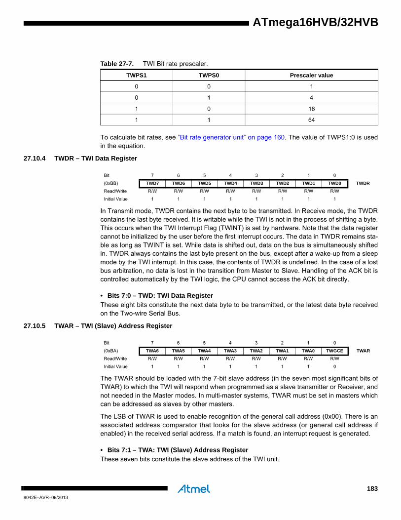
ATmega16HVB/32HVB
To calculate bit rates, see ”Bit rate generator unit” on page 160. The value of TWPS1:0 is usedin the equation.
27.10.4 TWDR – TWI Data Register
In Transmit mode, TWDR contains the next byte to be transmitted. In Receive mode, the TWDRcontains the last byte received. It is writable while the TWI is not in the process of shifting a byte.This occurs when the TWI Interrupt Flag (TWINT) is set by hardware. Note that the data registercannot be initialized by the user before the first interrupt occurs. The data in TWDR remains sta-ble as long as TWINT is set. While data is shifted out, data on the bus is simultaneously shiftedin. TWDR always contains the last byte present on the bus, except after a wake-up from a sleepmode by the TWI interrupt. In this case, the contents of TWDR is undefined. In the case of a lostbus arbitration, no data is lost in the transition from Master to Slave. Handling of the ACK bit iscontrolled automatically by the TWI logic, the CPU cannot access the ACK bit directly.
• Bits 7:0 – TWD: TWI Data Register
These eight bits constitute the next data byte to be transmitted, or the latest data byte receivedon the Two-wire Serial Bus.
27.10.5 TWAR – TWI (Slave) Address Register
The TWAR should be loaded with the 7-bit slave address (in the seven most significant bits ofTWAR) to which the TWI will respond when programmed as a slave transmitter or Receiver, andnot needed in the Master modes. In multi-master systems, TWAR must be set in masters whichcan be addressed as slaves by other masters.
The LSB of TWAR is used to enable recognition of the general call address (0x00). There is anassociated address comparator that looks for the slave address (or general call address ifenabled) in the received serial address. If a match is found, an interrupt request is generated.
• Bits 7:1 – TWA: TWI (Slave) Address Register
These seven bits constitute the slave address of the TWI unit.
Table 27-7. TWI Bit rate prescaler.
TWPS1 TWPS0 Prescaler value
0 0 1
0 1 4
1 0 16
1 1 64
Bit 7 6 5 4 3 2 1 0
(0xBB) TWD7 TWD6 TWD5 TWD4 TWD3 TWD2 TWD1 TWD0 TWDR
Read/Write R/W R/W R/W R/W R/W R/W R/W R/W
Initial Value 1 1 1 1 1 1 1 1
Bit 7 6 5 4 3 2 1 0
(0xBA) TWA6 TWA5 TWA4 TWA3 TWA2 TWA1 TWA0 TWGCE TWAR
Read/Write R/W R/W R/W R/W R/W R/W R/W R/W
Initial Value 1 1 1 1 1 1 1 0
1838042E–AVR–09/2013
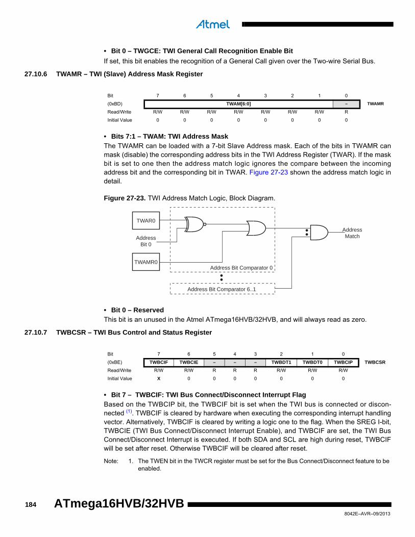
• Bit 0 – TWGCE: TWI General Call Recognition Enable Bit
If set, this bit enables the recognition of a General Call given over the Two-wire Serial Bus.
27.10.6 TWAMR – TWI (Slave) Address Mask Register
• Bits 7:1 – TWAM: TWI Address Mask
The TWAMR can be loaded with a 7-bit Slave Address mask. Each of the bits in TWAMR canmask (disable) the corresponding address bits in the TWI Address Register (TWAR). If the maskbit is set to one then the address match logic ignores the compare between the incomingaddress bit and the corresponding bit in TWAR. Figure 27-23 shown the address match logic indetail.
Figure 27-23. TWI Address Match Logic, Block Diagram.
• Bit 0 – Reserved
This bit is an unused in the Atmel ATmega16HVB/32HVB, and will always read as zero.
27.10.7 TWBCSR – TWI Bus Control and Status Register
• Bit 7 – TWBCIF: TWI Bus Connect/Disconnect Interrupt Flag
Based on the TWBCIP bit, the TWBCIF bit is set when the TWI bus is connected or discon-nected (1). TWBCIF is cleared by hardware when executing the corresponding interrupt handlingvector. Alternatively, TWBCIF is cleared by writing a logic one to the flag. When the SREG I-bit,TWBCIE (TWI Bus Connect/Disconnect Interrupt Enable), and TWBCIF are set, the TWI BusConnect/Disconnect Interrupt is executed. If both SDA and SCL are high during reset, TWBCIFwill be set after reset. Otherwise TWBCIF will be cleared after reset.
Note: 1. The TWEN bit in the TWCR register must be set for the Bus Connect/Disconnect feature to be enabled.
Bit 7 6 5 4 3 2 1 0
(0xBD) TWAM[6:0] – TWAMR
Read/Write R/W R/W R/W R/W R/W R/W R/W R
Initial Value 0 0 0 0 0 0 0 0
AddressMatch
Address Bit Comparator 0
Address Bit Comparator 6..1
TWAR0
TWAMR0
AddressBit 0
Bit 7 6 5 4 3 2 1 0
(0xBE) TWBCIF TWBCIE – – – TWBDT1 TWBDT0 TWBCIP TWBCSR
Read/Write R/W R/W R R R R/W R/W R/W
Initial Value X 0 0 0 0 0 0 0
1848042E–AVR–09/2013
ATmega16HVB/32HVB

ATmega16HVB/32HVB
• Bit 6 – TWBCIE: TWI Bus Connect/Disconnect Interrupt Enable
When the TWBCIE bit and the I-bit in the Status Register are set, the TWI Bus Connect/Discon-nect Interrupt is enabled. The corresponding interrupt is executed i f a TWI BusConnect/Disconnect occurs, that is, when the TWBCIE bit is set.
• Bit 5:3 – Reserved
These bits are reserved in the Atmel ATmega16HVB/32HVB and will always read as zero.
• Bit 2:1 – TWBDT1, TWBDT0: TWI Bus Disconnect Time-out Period
The TWBDT bits decides how long both the TWI data (SDA) and clock (SCL) signals must below before generating the TWI Bus Disconnect Interrupt. The different configuration values andtheir corresponding time-out periods are shown in Table 27-8.
• Bit 0 – TWBCIP: TWI Bus Connect/Disconnect Interrupt Polarity
The TWBCIP bit decide if the TWI Bus Connect/Disconnect Interrupt Flag (TWBCIF) should beset on a Bus Connect or a Bus Disconnect. If TWBCIP is cleared, the TWBCIF flag is set on aBus Connect. If TWBCIP is set, the TWBCIF flag is set on a Bus Disconnect.
Table 27-8. TW Bus disconnect time-out period.
TWBDT1 TWBDT0 TWI bus disconnect time-out period
0 0 250ms
0 1 500ms
1 0 1000ms
1 1 2000ms
1858042E–AVR–09/2013

28. debugWIRE on-chip debug system
28.1 Features
• Complete program flow control
• Emulates all øn-chip functions, both digital and analog, except RESET pin
• Real-time operation
• Symbolic debugging support (both at C and Assembler source level, or for other HLLs)
• Unlimited number of program break points (using software break points)
• Non-intrusive operation
• Electrical characteristics identical to real device
• Automatic configuration system
• High-speed operation
• Programming of non-volatile memories
28.2 Overview
The debugWIRE On-chip debug system uses a One-wire, bi-directional interface to control theprogram flow, execute AVR instructions in the CPU and to program the different non-volatilememories.
28.3 Physical interface
When the debugWIRE Enable (DWEN) Fuse is programmed and Lock bits are unprogrammed,the debugWIRE system within the target device is activated. The RESET port pin is configuredas a wire-AND (open-drain) bi-directional I/O pin with pull-up enabled and becomes the commu-nication gateway between target and emulator.
Figure 28-1. The debugWIRE setup.
Figure 28-1 shows the schematic of a target MCU, with debugWIRE enabled, and the emulatorconnector. The system clock is not affected by debugWIRE and will always be the clock sourceselected by the OSCSEL Fuses.
dW
GND
dW(RESET)
VCC
1.8 - 5.5V
dW
GND
dW(RESET)
VCC
3.0V - 4.5V
1868042E–AVR–09/2013
ATmega16HVB/32HVB

ATmega16HVB/32HVB
When designing a system where debugWIRE will be used, the following observations must bemade for correct operation:
• Pull-up resistors on the dW/(RESET) line must not be smaller than 10k. The pull-up resistor is not required for debugWIRE functionality
• Connecting the RESET pin directly to VCC will not work
• Capacitors connected to the RESET pin must be disconnected when using debugWire
• All external reset sources must be disconnected
28.4 Software break points
debugWIRE supports Program memory Break Points by the AVR Break instruction. Setting aBreak Point in AVR Studio® will insert a BREAK instruction in the Program memory. The instruc-tion replaced by the BREAK instruction will be stored. When program execution is continued, thestored instruction will be executed before continuing from the Program memory. A break can beinserted manually by putting the BREAK instruction in the program.
The Flash must be re-programmed each time a Break Point is changed. This is automaticallyhandled by AVR Studio through the debugWIRE interface. The use of Break Points will thereforereduce the Flash Data retention. Devices used for debugging purposes should not be shipped toend customers.
28.5 Limitations of debugWIRE
The debugWIRE communication pin (dW) is physically located on the same pin as ExternalReset (RESET). An External Reset source is therefore not supported when the debugWIRE isenabled.
A programmed DWEN Fuse enables some parts of the clock system to be running in all sleepmodes. This will increase the power consumption while in sleep. Thus, the DWEN Fuse shouldbe disabled when debugWire is not used.
When using debugWIRE to access the flash (reading/writing), one must make sure theSPMCSR register is not locked from before. If SPMCSR is locked the result of the operation maynot be as expected.
28.6 Register description
The following section describes the registers used with the debugWire.
28.6.1 DWDR – debugWire Data Register
The DWDR Register provides a communication channel from the running program in the MCUto the debugger. This register is only accessible by the debugWIRE and can therefore not beused as a general purpose register in the normal operations.
Bit 7 6 5 4 3 2 1 0
0x31 (0x51) DWDR[7:0] DWDR
Read/Write R/W R/W R/W R/W R/W R/W R/W R/W
Initial Value 0 0 0 0 0 0 0 0
1878042E–AVR–09/2013

29. Boot loader support – Read-while-write self-programming
29.1 Features• Read-while-write self-programming
• Flexible boot memory size
• High security (separate boot lock bits for a flexible protection)
• Separate fuse to select reset vector
• Optimized page (1) size
• Code efficient algorithm
• Efficient read-modify-write support
Note: 1. A page is a section in the Flash consisting of several bytes (see ”Page size” on page 207) used during programming. The page organization does not affect normal operation.
29.2 Overview
The Boot Loader Support provides a real Read-While-Write Self-Programming mechanism fordownloading and uploading program code by the MCU itself. This feature allows flexible applica-tion software updates controlled by the MCU using a Flash-resident Boot Loader program. TheBoot Loader program can use any available data interface and associated protocol to read codeand write (program) that code into the Flash memory, or read the code from the program mem-ory. The program code within the Boot Loader section has the capability to write into the entireFlash, including the Boot Loader memory. The Boot Loader can thus even modify itself, and itcan also erase itself from the code if the feature is not needed anymore. The size of the BootLoader memory is configurable with fuses and the Boot Loader has two separate sets of BootLock bits which can be set independently. This gives the user a unique flexibility to select differ-ent levels of protection.
29.3 Application and boot loader flash sectionsThe Flash memory is organized in two main sections, the Application section and the BootLoader section. The size of the different sections is configured by the BOOTSZ Fuses as shownin Table 29-5 on page 200 and Figure 29-2 on page 191. These two sections can have differentlevel of protection since they have different sets of Lock bits.
29.3.1 Application section
The Application section is the section of the Flash that is used for storing the application code.The protection level for the Application section can be selected by the application Boot Lock bits(Boot Lock bits 0), see Table 30-2 on page 204. The Application section can never store anyBoot Loader code since the SPM instruction is disabled when executed from the Applicationsection.
29.3.2 BLS – Boot loader section
While the Application section is used for storing the application code, the The Boot Loader soft-ware must be located in the BLS since the SPM instruction can initiate a programming whenexecuting from the BLS only. The SPM instruction can access the entire Flash, including theBLS itself. The protection level for the Boot Loader section can be selected by the Boot LoaderLock bits (Boot Lock bits 1), see Table 30-2 on page 204.
1888042E–AVR–09/2013
ATmega16HVB/32HVB

ATmega16HVB/32HVB
29.4 Read-while-write and no read-while-write flash sectionsWhether the CPU supports Read-While-Write or if the CPU is halted during a Boot Loader soft-ware update is dependent on which address that is being programmed. In addition to the twosections that are configurable by the BOOTSZ Fuses as described above, the Flash is alsodivided into two fixed sections, the Read-While-Write (RWW) section and the No Read-While-Write (NRWW) section. The limit between the RWW- and NRWW sections is given in Table 29-6 on page 200 and Figure 29-2 on page 191. The main difference between the two sections is:
• When erasing or writing a page located inside the RWW section, the NRWW section can be read during the operation
• When erasing or writing a page located inside the NRWW section, the CPU is halted during the entire operation
Note that the user software can never read any code that is located inside the RWW section dur-ing a Boot Loader software operation. The syntax “Read-While-Write section” refers to whichsection that is being programmed (erased or written), not which section that actually is beingread during a Boot Loader software update.
29.4.1 RWW – Read-while-write section
If a Boot Loader software update is programming a page inside the RWW section, it is possibleto read code from the Flash, but only code that is located in the NRWW section. During an on-going programming, the software must ensure that the RWW section never is being read. If theuser software is trying to read code that is located inside the RWW section (that is, by acall/jmp/lpm or an interrupt) during programming, the software might end up in an unknownstate. To avoid this, the interrupts should either be disabled or moved to the Boot Loader sec-tion. The Boot Loader section is always located in the NRWW section. The RWW Section Busybit (RWWSB) in the Store Program Memory Control and Status Register (SPMCSR) will be readas logical one as long as the RWW section is blocked for reading. After a programming is com-pleted, the RWWSB must be cleared by software before reading code located in the RWWsection. See ”SPMCSR – Store Program Memory Control and Status Register” on page 202 fordetails on how to clear RWWSB.
29.4.2 NRWW – No read-while-write section
The code located in the NRWW section can be read when the Boot Loader software is updatinga page in the RWW section. When the Boot Loader code updates the NRWW section, the CPUis halted during the entire Page Erase or Page Write operation.
Table 29-1. Read-while-write features.
Which section does the Z-pointer address during the programming?
Which section can be read during programming?
CPUhalted?
Read-while-writesupported?
RWW section NRWW section No Yes
NRWW section None Yes No
1898042E–AVR–09/2013
Figure 29-1. Read-while-write vs. no read-while-write.
Read-While-Write(RWW) Section
No Read-While-Write (NRWW) Section
Z-pointerAddresses RWWSection
Z-pointerAddresses NRWWSection
CPU is HaltedDuring the Operation
Code Located in NRWW SectionCan be Read Duringthe Operation
1908042E–AVR–09/2013
ATmega16HVB/32HVB

ATmega16HVB/32HVB
Figure 29-2. Memory sections.
Note: 1. The parameters in the figure above are given in Table 29-5 on page 200.
29.5 Boot loader lock bitsIf no Boot Loader capability is needed, the entire Flash is available for application code. TheBoot Loader has two separate sets of Boot Lock bits which can be set independently. This givesthe user a unique flexibility to select different levels of protection.
The user can select:
• To protect the entire Flash from a software update by the MCU
• To protect only the Boot Loader Flash section from a software update by the MCU
• To protect only the Application Flash section from a software update by the MCU
• Allow software update in the entire Flash
See Table 30-2 on page 204 for further details. The Boot Lock bits can be set in software and inSerial or Parallel Programming mode, but they can be cleared by a Chip Erase command only.The general Write Lock (Lock Bit mode 2) does not control the programming of the Flash mem-ory by SPM instruction. Similarly, the general Read/Write Lock (Lock Bit mode 1) does notcontrol reading nor writing by LPM/SPM, if it is attempted.
0x0000
Flashend
Program MemoryBOOTSZ = '11'
Application Flash Section
Boot Loader Flash SectionFlashend
Program MemoryBOOTSZ = '10'
0x0000
Program MemoryBOOTSZ = '01'
Program MemoryBOOTSZ = '00'
Application Flash Section
Boot Loader Flash Section
0x0000
Flashend
Application Flash Section
Flashend
End RWW
Start NRWW
Application Flash Section
Boot Loader Flash Section
Boot Loader Flash Section
End RWW
Start NRWW
End RWW
Start NRWW
0x0000
End RWW, End Application
Start NRWW, Start Boot Loader
Application Flash SectionApplication Flash Section
Application Flash Section
Rea
d-W
hile
-Writ
e S
ectio
nN
o R
ead-
Whi
le-W
rite
Sec
tion
Rea
d-W
hile
-Writ
e S
ectio
nN
o R
ead-
Whi
le-W
rite
Sec
tion
Rea
d-W
hile
-Writ
e S
ectio
nN
o R
ead-
Whi
le-W
rite
Sec
tion
Rea
d-W
hile
-Writ
e S
ectio
nN
o R
ead-
Whi
le-W
rite
Sec
tion
End Application
Start Boot Loader
End Application
Start Boot Loader
End Application
Start Boot Loader
1918042E–AVR–09/2013
29.6 Entering the boot loader programEntering the Boot Loader takes place by a jump or call from the application program. This maybe initiated by a trigger such as a command received via the TWI interface. Alternatively, theBoot Reset Fuse can be programmed so that the Reset Vector is pointing to the Boot Flash startaddress after a reset. In this case, the Boot Loader is started after a reset. After the applicationcode is loaded, the program can start executing the application code. Note that the fuses cannotbe changed by the MCU itself. This means that once the Boot Reset Fuse is programmed, theReset Vector will always point to the Boot Loader Reset and the fuse can only be changedthrough the serial or parallel programming interface.
Note: 1. “1” means unprogrammed, “0” means programmed.
29.7 Addressing the flash during self-programmingThe Z-pointer is used to address the SPM commands.
Since the Flash is organized in pages (see ”Fuse bits” on page 205), the Program Counter canbe treated as having two different sections. One section, consisting of the least significant bits, isaddressing the words within a page, while the most significant bits are addressing the pages.This is shown in Figure 29-3 on page 193. Note that the Page Erase and Page Write operationsare addressed independently. Therefore it is of major importance that the Boot Loader softwareaddresses the same page in both the Page Erase and Page Write operation. Once a program-ming operation is initiated, the address is latched and the Z-pointer can be used for otheroperations.
The only SPM operation that does not use the Z-pointer is Setting the Boot Loader Lock bits.The content of the Z-pointer is ignored and will have no effect on the operation. The LPMinstruction does also use the Z-pointer to store the address. Since this instruction addresses theFlash byte-by-byte, also the LSB (bit Z0) of the Z-pointer is used.
Table 29-2. Boot Reset Fuse (1).
BOOTRST Reset address
1 Reset vector = Application reset (address 0x0000)
0 Reset vector = Boot loader reset (see Table 29-5 on page 200)
Bit 15 14 13 12 11 10 9 8
ZH (R31) Z15 Z14 Z13 Z12 Z11 Z10 Z9 Z8
ZL (R30) Z7 Z6 Z5 Z4 Z3 Z2 Z1 Z0
7 6 5 4 3 2 1 0
1928042E–AVR–09/2013
ATmega16HVB/32HVB

ATmega16HVB/32HVB
Figure 29-3. Addressing the flash during SPM (1).
Note: 1. The different variables used in Figure 29-3 are listed in Table 29-7 on page 200 and Table 29-10 on page 201.
29.8 Self-programming the flashThe program memory is updated in a page by page fashion. Before programming a page withthe data stored in the temporary page buffer, the page must be erased. The temporary page buf-fer is filled one word at a time using SPM and the buffer can be filled either before the PageErase command or between a Page Erase and a Page Write operation:
Alternative one, fill the buffer before a Page Erase:
• Fill temporary page buffer
• Perform a Page Erase
• Perform a Page Write
Alternative two, fill the buffer after Page Erase:
• Perform a Page Erase
• Fill temporary page buffer
• Perform a Page Write
If only a part of the page needs to be changed, the rest of the page must be stored (for examplein the temporary page buffer) before the erase, and then be rewritten. When using alternative 1,the Boot Loader provides an effective Read-Modify-Write feature which allows the user softwareto first read the page, do the necessary changes, and then write back the modified data. If alter-native 2 is used, it is not possible to read the old data while loading since the page is alreadyerased. The temporary page buffer can be accessed in a random sequence. It is essential thatthe page address used in both the Page Erase and Page Write operation is addressing thesame page. See ”Simple assembly code example for a boot loader” on page 198 for an assem-bly code example.
PROGRAM MEMORY
0115
Z - REGISTER
BIT
0
ZPAGEMSB
WORD ADDRESSWITHIN A PAGE
PAGE ADDRESSWITHIN THE FLASH
ZPCMSB
INSTRUCTION WORD
PAGE PCWORD[PAGEMSB:0]:
00
01
02
PAGEEND
PAGE
PCWORDPCPAGE
PCMSB PAGEMSBPROGRAMCOUNTER
1938042E–AVR–09/2013

29.8.1 Performing page erase by SPM
To execute Page Erase, set up the address in the Z-pointer, write “X0000011” to SPMCSR andexecute SPM within four clock cycles after writing SPMCSR. The data in R1 and R0 is ignored.The page address must be written to PCPAGE in the Z-register. Other bits in the Z-pointer willbe ignored during this operation.
• Page Erase to the RWW section: The NRWW section can be read during the Page Erase
• Page Erase to the NRWW section: The CPU is halted during the operation
29.8.2 Filling the temporary buffer (page loading)
To write an instruction word, set up the address in the Z-pointer and data in R1:R0, write“X0000001” to SPMCSR and execute SPM within four clock cycles after writing SPMCSR. Thecontent of PCWORD in the Z-register is used to address the data in the temporary buffer. Thetemporary buffer will auto-erase after a Page Write operation or by writing the RWWSRE bit inSPMCSR. It is also erased after a system reset. Note that it is not possible to write more thanone time to each address without erasing the temporary buffer.
29.8.3 Performing a page write
To execute Page Write, set up the address in the Z-pointer, write “X0000101” to SPMCSR andexecute SPM within four clock cycles after writing SPMCSR. The data in R1 and R0 is ignored.The page address must be written to PCPAGE. Other bits in the Z-pointer will be ignored duringthis operation.
• Page Write to the RWW section: The NRWW section can be read during the Page Write
• Page Write to the NRWW section: The CPU is halted during the operation
29.8.4 Using the SPM interrupt
If the SPM interrupt is enabled, the SPM interrupt will generate a constant interrupt when theSPMEN bit in SPMCSR is cleared. This means that the interrupt can be used instead of pollingthe SPMCSR Register in software. When using the SPM interrupt, the Interrupt Vectors shouldbe moved to the BLS section to avoid that an interrupt is accessing the RWW section when it isblocked for reading. How to move the interrupts is described in ”Interrupts” on page 52.
29.8.5 Consideration while updating BLS
Special care must be taken if the user allows the Boot Loader section to be updated by leavingBoot Lock bit11 unprogrammed. An accidental write to the Boot Loader itself can corrupt theentire Boot Loader, and further software updates might be impossible. If it is not necessary tochange the Boot Loader software itself, it is recommended to program the Boot Lock bit11 toprotect the Boot Loader software from any internal software changes.
29.8.6 Prevent reading the RWW section during self-programming
During Self-Programming (either Page Erase or Page Write), the RWW section is alwaysblocked for reading. The user software itself must prevent that this section is addressed duringthe self programming operation. The RWWSB in the SPMCSR will be set as long as the RWWsection is busy. During Self-Programming the Interrupt Vector table should be moved to the BLSas described in ”Interrupts” on page 52, or the interrupts must be disabled. Before addressingthe RWW section after the programming is completed, the user software must clear theRWWSB by writing the RWWSRE. See ”Simple assembly code example for a boot loader” onpage 198 for an example.
1948042E–AVR–09/2013
ATmega16HVB/32HVB

ATmega16HVB/32HVB
29.8.7 Setting the lock bits by SPM
To set the Lock bits, write the desired data to R0, write “X0001001” to SPMCSR and executeSPM within four clock cycles after writing SPMCSR.
See Table 30-2 on page 204 for how the different settings of the Lock bits affect the Flashaccess.
If bits 5:0 in R0 are cleared (zero), the corresponding Lock bit will be programmed if an SPMinstruction is executed within four cycles after LBSET and SPMEN are set in SPMCSR. The Z-pointer is don’t care during this operation, but for future compatibility it is recommended to loadthe Z-pointer with 0x0001 (same as used for reading the lOck bits). For future compatibility it isalso recommended to set bits 7 and 6 in R0 to “1” when writing the Lock bits. When program-ming the Lock bits the entire Flash can be read during the operation.
29.8.8 Reading the fuse and lock bits from software
It is possible to read both the Fuse and Lock bits from software. To read the Lock bits, load theZ-pointer with 0x0001 and set the LBSET and SPMEN bits in SPMCSR. When an LPM instruc-tion is executed within three CPU cycles after the LBSET and SPMEN bits are set in SPMCSR,the value of the Lock bits will be loaded in the destination register. The LBSET and SPMEN bitswill auto-clear upon completion of reading the Lock bits. When LBSET and SPMEN are cleared,LPM will work as described in the ”AVR Instruction Set” description.
The algorithm for reading the Fuse Low byte is similar to the one described above for readingthe Lock bits. To read the Fuse Low byte, load the Z-pointer with 0x0000 and set the LBSET andSPMEN bits in SPMCSR. When an LPM instruction is executed within three cycles after theLBSET and SPMEN bits are set in the SPMCSR, the value of the Fuse Low byte (FLB) will beloaded in the destination register as shown below. Refer to Table 30-4 on page 206 for adetailed description and mapping of the Fuse Low byte.
Similarly, when reading the Fuse High byte, load 0x0003 in the Z-pointer. When an LPM instruc-tion is executed within three cycles after the LBSET and SPMEN bits are set in the SPMCSR,the value of the Fuse High byte (FHB) will be loaded in the destination register as shown below.Refer to Table 30-3 on page 205 for detailed description and mapping of the Fuse High byte.
Fuse and Lock bits that are programmed, will be read as zero. Fuse and Lock bits that areunprogrammed, will be read as one.
29.8.9 Reading the signature row from software
To read the Signature Row from software, load the Z-pointer with the signature byte addressgiven in Table 29-3 on page 196 and set the SIGRD and SPMEN bits in SPMCSR. When anLPM instruction is executed within three CPU cycles after the SIGRD and SPMEN bits are set inSPMCSR, the signature byte value will be loaded in the destination register. The SIGRD andSPMEN bits will auto-clear 6 cycles after writing to SPMCSR, which is locked for further writing
Bit 7 6 5 4 3 2 1 0
R0 1 1 BLB12 BLB11 BLB02 BLB01 LB2 LB1
Bit 7 6 5 4 3 2 1 0
Rd – – BLB12 BLB11 BLB02 BLB01 LB2 LB1
Bit 7 6 5 4 3 2 1 0
Rd FLB7 FLB6 FLB5 FLB4 FLB3 FLB2 FLB1 FLB0
Bit 7 6 5 4 3 2 1 0
Rd FHB7 FHB6 FHB5 FHB4 FHB3 FHB2 FHB1 FHB0
1958042E–AVR–09/2013

during these cycles. When SIGRD and SPMEN are cleared, LPM will work as described in theInstruction set Manual.
Table 29-3. Signature row addressing.
Signature byte description Z-pointer address
Device ID 0, manufacture ID 00H
Device ID 1, flash size 02H
Device ID 2, device 04H
FOSCCAL (1) 01H
FOSC SEGMENT (2) 03H
Reserved 05H
SLOW RC period L 06H
SLOW RC period H (3) 07H
SLOW RC temp prediction L 08H
SLOW RC temp prediction H (4) 09H
ULP RC FRQ (5) 0AH
SLOW RC FRQ (6) 0BH
ULP RC temp prediction coefficient L OCH
ULP RC temp prediction coefficient H (7) ODH
ULP RC period L OEH
ULP RC period H (8) OFH
BGCRR calibration byte 10H
BGCCR calibration byte 11H
Reserved 12H:17H
VPTAT CAL L 18H
VPTAT CAL H (9) 19H
V-ADC Cell1 gain calibration word L 1AH
V-ADC Cell1 gain calibration word H (10) 1BH
V-ADC Cell2 gain calibration word L 1CH
V-ADC Cell2 gain calibration word H (10) 1DH
V-ADC Cell3 gain calibration word L 1EH
V-ADC Cell3 gain calibration word H (10) 1FH
V-ADC Cell4 gain calibration word L 20H
V-ADC Cell4 gain calibration word H (10) 21H
V-ADC Cell1 offset (11) 22H
V-ADC Cell2 offset (11) 23H
V-ADC Cell3 offset (11) 24H
V-ADC Cell4 offset (11) 25H
V-ADC0 gain calibration word L 26H
1968042E–AVR–09/2013
ATmega16HVB/32HVB

ATmega16HVB/32HVB
Notes: 1. Default FOSCCAL value after reset.2. FOSCCAL setting used to smooth the transition from one segment to the next when calibrating
the Fast RC oscillator.3. 8 prescaled Slow RC periods in µs using the Oscillator Sampling Interface (@THOT°C).4. Slow RC oscillator frequency temperature drift prediction value.5. ULP RC oscillator frequency in kHz (@ THOT°C).6. Slow RC oscillator frequency in kHz (@THOT°C).7. ULP RC oscillator frequency temperature drift prediction value.8. 8 prescaled ULP RC periods in µs using the Oscillator Sampling Interface (@THOT°C).9. Calibration word used to calculate the absolute temperature in Kelvin from a VTEMP
conversion.10. Calibration word used to compensate for gain error in V-ADC Cells.11. Calibration byte used to compensate for offset in V-ADC Cells.12. Calibration word used to compensate for gain error in ADC0.13. Calibration word used to compensate for gain error in ADC1.14. Calibration byte used to compensate for offset in ADC0 and ADC1.15. Hot temperature used for factory calibration in °C.16. Atmel does not test that the combination of lot ID and position is unique.
All other addresses are reserved for future use.
29.8.10 SPMCSR writing restrictions
Writing any other combination than “100001”, “010001”, “001001”, “000101”, “000011” or“000001” in the lower six bits will have no effect.
SPMCSR is locked for writing under the following conditions:
• One or more of the bits 5:0 in SPMCSR is set to 1
• During EEPROM write (status bit EEWE in EECR is set)
SPMCSR will be cleared at the following events:
• on completion of successful execution the following instructions:
– LPM with LBSET and SPMEN set
– SPM with LBSET and SPMEN set
– SPM with PGERS and SPMEN set
– SPM with PGWRT and SPMEN set
– SPM with SPMEN set
• six cycles after writing SPMCSR if any other or no LPM/SPM is executed
V-ADC0 gain calibration word H (12) 27H
V-ADC1 gain calibration word L 28H
V-ADC1 gain calibration word H (13) 29H
V-ADC ADC0 offset (14) 2AH
V-ADC ADC1 offset (14) 2BH
Reserved 2CH:2FH
THOT (15) 30H
Device lot ID and position (16) 4AH:53H
Table 29-3. Signature row addressing. (Continued)
Signature byte description Z-pointer address
1978042E–AVR–09/2013

29.8.11 Programming time for flash when using SPM
The Fast RC Oscillator is used to time Flash accesses. Table 29-4 shows the typical program-ming time for Flash accesses from the CPU.
Note: 1. Minimum and maximum programming time is per individual operation.
29.8.12 Simple assembly code example for a boot loader;-the routine writes one page of data from RAM to Flash; the first data location in RAM is pointed to by the Y pointer; the first data location in Flash is pointed to by the Z-pointer;-error handling is not included;-the routine must be placed inside the Boot space; (at least the Do_spm sub routine). Only code inside NRWW section ; can be read during Self-Programming (Page Erase and Page Write).;-registers used: r0, r1, temp1 (r16), temp2 (r17), looplo (r24), ; loophi (r25), spmcrval (r20); storing and restoring of registers is not included in the routine; register usage can be optimized at the expense of code size;-It is assumed that either the interrupt table is moved to the ; Boot loader section or that the interrupts are disabled.
.equ PAGESIZEB = PAGESIZE*2 ;PAGESIZEB is page size in BYTES, not words
.org SMALLBOOTSTARTWrite_page:; Page Eraseldi spmcrval, (1<<PGERS) | (1<<SPMEN)call Do_spm
; re-enable the RWW sectionldi spmcrval, (1<<RWWSRE) | (1<<SPMEN)call Do_spm
; transfer data from RAM to Flash page bufferldi looplo, low(PAGESIZEB) ;init loop variableldi loophi, high(PAGESIZEB) ;not required for PAGESIZEB<=256
Wrloop:ld r0, Y+ld r1, Y+ldi spmcrval, (1<<SPMEN)call Do_spmadiw ZH:ZL, 2sbiw loophi:looplo, 2 ;use subi for PAGESIZEB<=256brne Wrloop
; execute Page Writesubi ZL, low(PAGESIZEB) ;restore pointersbci ZH, high(PAGESIZEB) ;not required for PAGESIZEB<=256ldi spmcrval, (1<<PGWRT) | (1<<SPMEN)call Do_spm
; re-enable the RWW sectionldi spmcrval, (1<<RWWSRE) | (1<<SPMEN)
Table 29-4. SPM Programming Time (1).
Symbol Min programming time Max programming time
Flash write (Page Erase, Page Write, and write Lock bits by SPM)
3.7ms 4.5ms
1988042E–AVR–09/2013
ATmega16HVB/32HVB

ATmega16HVB/32HVB
call Do_spm
; read back and check, optionalldi looplo, low(PAGESIZEB) ;init loop variableldi loophi, high(PAGESIZEB) ;not required for PAGESIZEB<=256subi YL, low(PAGESIZEB) ;restore pointersbci YH, high(PAGESIZEB)
Rdloop:lpm r0, Z+ld r1, Y+cpse r0, r1jmp Errorsbiw loophi:looplo, 1 ;use subi for PAGESIZEB<=256brne Rdloop; return to RWW section; verify that RWW section is safe to read
Return:in temp1, SPMCSRsbrs temp1, RWWSB ; If RWWSB is set, the RWW section is not ready yetret; re-enable the RWW sectionldi spmcrval, (1<<RWWSRE) | (1<<SPMEN)call Do_spmrjmp Return
Do_spm:; check for previous SPM complete
Wait_spm:in temp1, SPMCSRsbrc temp1, SPMENrjmp Wait_spm; input: spmcrval determines SPM action; disable interrupts if enabled, store statusin temp2, SREGcli; check that no EEPROM write access is present
Wait_ee:sbic EECR, EEWErjmp Wait_ee; SPM timed sequenceout SPMCSR, spmcrvalspm; restore SREG (to enable interrupts if originally enabled)out SREG, temp2ret
1998042E–AVR–09/2013
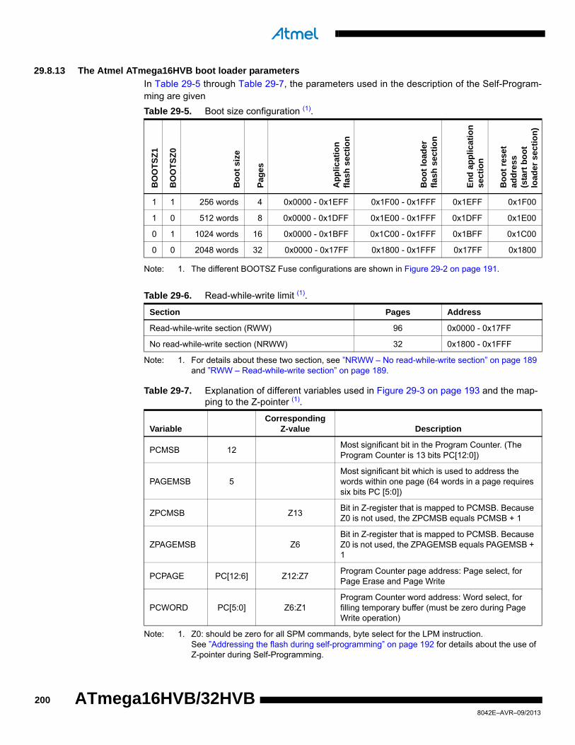
29.8.13 The Atmel ATmega16HVB boot loader parameters
In Table 29-5 through Table 29-7, the parameters used in the description of the Self-Program-ming are given
Note: 1. The different BOOTSZ Fuse configurations are shown in Figure 29-2 on page 191.
Note: 1. For details about these two section, see ”NRWW – No read-while-write section” on page 189 and ”RWW – Read-while-write section” on page 189.
Note: 1. Z0: should be zero for all SPM commands, byte select for the LPM instruction.See ”Addressing the flash during self-programming” on page 192 for details about the use of Z-pointer during Self-Programming.
Table 29-5. Boot size configuration (1).
BO
OT
SZ
1
BO
OT
SZ
0
Bo
ot
size
Pag
es
Ap
plic
atio
nfl
ash
se
ctio
n
Bo
ot
load
erfl
ash
se
ctio
n
En
d a
pp
lica
tio
nse
cti
on
Bo
ot
rese
tad
dre
ss(s
tart
bo
ot
load
er s
ect
ion
)
1 1 256 words 4 0x0000 - 0x1EFF 0x1F00 - 0x1FFF 0x1EFF 0x1F00
1 0 512 words 8 0x0000 - 0x1DFF 0x1E00 - 0x1FFF 0x1DFF 0x1E00
0 1 1024 words 16 0x0000 - 0x1BFF 0x1C00 - 0x1FFF 0x1BFF 0x1C00
0 0 2048 words 32 0x0000 - 0x17FF 0x1800 - 0x1FFF 0x17FF 0x1800
Table 29-6. Read-while-write limit (1).
Section Pages Address
Read-while-write section (RWW) 96 0x0000 - 0x17FF
No read-while-write section (NRWW) 32 0x1800 - 0x1FFF
Table 29-7. Explanation of different variables used in Figure 29-3 on page 193 and the map-ping to the Z-pointer (1).
VariableCorresponding
Z-value Description
PCMSB 12Most significant bit in the Program Counter. (The Program Counter is 13 bits PC[12:0])
PAGEMSB 5Most significant bit which is used to address the words within one page (64 words in a page requires six bits PC [5:0])
ZPCMSB Z13Bit in Z-register that is mapped to PCMSB. Because Z0 is not used, the ZPCMSB equals PCMSB + 1
ZPAGEMSB Z6Bit in Z-register that is mapped to PCMSB. Because Z0 is not used, the ZPAGEMSB equals PAGEMSB + 1
PCPAGE PC[12:6] Z12:Z7Program Counter page address: Page select, for Page Erase and Page Write
PCWORD PC[5:0] Z6:Z1Program Counter word address: Word select, for filling temporary buffer (must be zero during Page Write operation)
2008042E–AVR–09/2013
ATmega16HVB/32HVB

ATmega16HVB/32HVB
29.8.14 The Atmel ATmega32HVB boot loader parameters
In Table 29-8 through Table 29-10, the parameters used in the description of the Self-Program-ming are given
Note: 1. The different BOOTSZ Fuse configurations are shown in Figure 29-2 on page 191.
For details about these two section, see ”NRWW – No read-while-write section” on page 189 and ”RWW –
Read-while-write section” on page 189.
Note: 1. Z0: should be zero for all SPM commands, byte select for the LPM instruction.See ”Addressing the flash during self-programming” on page 192 for details about the use of Z-pointer during Self-Programming.
Table 29-8. Boot size configuration (1).
BO
OT
SZ
1
BO
OT
SZ
0
Bo
ot
size
Pag
es
Ap
plic
atio
nfl
ash
se
ctio
n
Bo
ot
load
erfl
ash
se
ctio
n
En
d a
pp
lica
tio
nse
cti
on
Bo
ot
rese
tad
dre
ss(s
tart
bo
ot
load
er s
ect
ion
)
1 1 256 words 4 0x0000 - 0x3EFF 0x3F00 - 0x3FFF 0x3EFF 0x3F00
1 0 512 words 8 0x0000 - 0x3DFF 0x3E00 - 0x3FFF 0x3DFF 0x3E00
0 1 1024 words 16 0x0000 - 0x3BFF 0x3C00 - 0x3FFF 0x3BFF 0x3C00
0 0 2048 words 32 0x0000 - 0x37FF 0x3800 - 0x3FFF 0x37FF 0x3800
Table 29-9. Read-while-write limit (1).
Section Pages Address
Read-while-write section (RWW) 224 0x0000 - 0x37FF
No read-while-write section (NRWW) 32 0x3800 - 0x3FFF
Table 29-10. Explanation of different variables used in Figure 29-3 on page 193 and the map-ping to the Z-pointer (1).
VariableCorresponding
Z-value Description
PCMSB 13Most significant bit in the Program Counter. (The Program Counter is 14 bits PC[13:0])
PAGEMSB 5Most significant bit which is used to address the words within one page (64 words in a page requires six bits PC [5:0])
ZPCMSB Z14Bit in Z-register that is mapped to PCMSB. Because Z0 is not used, the ZPCMSB equals PCMSB + 1
ZPAGEMSB Z6Bit in Z-register that is mapped to PCMSB. Because Z0 is not used, the ZPAGEMSB equals PAGEMSB + 1
PCPAGE PC[13:6] Z13:Z7Program Counter page address: Page select, for Page Erase and Page Write
PCWORD PC[5:0] Z6:Z1Program Counter word address: Word select, for filling temporary buffer (must be zero during Page Write operation)
2018042E–AVR–09/2013

29.9 Register description
29.9.1 SPMCSR – Store Program Memory Control and Status Register
The Store Program Memory Control and Status Register contains the control bits needed to con-trol the Boot Loader operations:
• Bit 7 – SPMIE: SPM Interrupt Enable
When the SPMIE bit is written to one, and the I-bit in the Status Register is set (one), the SPMready interrupt will be enabled. The SPM ready Interrupt will be executed as long as the SPMENbit in the SPMCSR Register is cleared.
• Bit 6 – RWWSB: Read-While-Write Section Busy
When a Self-Programming (Page Erase or Page Write) operation to the RWW section is initi-ated, the RWWSB will be set (one) by hardware. When the RWWSB bit is set, the RWW sectioncannot be accessed. The RWWSB bit will be cleared if the RWWSRE bit is written to one after aSelf-Programming operation is completed. Alternatively the RWWSB bit will automatically becleared if a page load operation is initiated.
• Bit 5 - SIGRD: Signature Row Read
If this bit is written to one at the same time as SPMEN, the next LPM instruction within threeclock cycles will read a byte from the signature row into the destination register. See ”Readingthe signature row from software” on page 195 for details.
An SPM instruction within four cycles after SIGRD and SPMEN are set will have no effect. Thisoperation is reserved for future use and should not be used.
• Bit 4 – RWWSRE: Read-While-Write Section Read Enable
When programming (Page Erase or Page Write) to the RWW section, the RWW section isblocked for reading (the RWWSB will be set by hardware). To re-enable the RWW section, theuser software must wait until the programming is completed (SPMEN will be cleared). Then, ifthe RWWSRE bit is written to one at the same time as SPMEN, the next SPM instruction withinfour clock cycles re-enables the RWW section. The RWW section cannot be re-enabled whilethe Flash is busy with a Page Erase or a Page Write (SPMEN is set). If the RWWSRE bit is writ-ten while the Flash is being loaded, the Flash load operation will abort and the data loaded willbe lost.
• Bit 3 – LBSET: Lock Bit Set
If this bit is written to one at the same time as SPMEN, the next SPM instruction within four clockcycles sets Lock bits, according to the data in R0. The data in R1 and the address in the Z-pointer are ignored. The LBSET bit will automatically be cleared upon completion of the Lock bitset, or after six cycles if no SPM instruction is executed within four clock cycles.
An LPM instruction within three cycles after LBSET and SPMEN are set in the SPMCSR Regis-ter, will read either the Lock bits or the Fuse bits (depending on Z0 in the Z-pointer) into thedestination register. See ”Reading the fuse and lock bits” on page 218 for details.
Bit 7 6 5 4 3 2 1 0
0x37 (0x57) SPMIE RWWSB SIGRD RWWSRE LBSET PGWRT PGERS SPMEN SPMCSR
Read/Write R/W R R/W R/W R/W R/W R/W R/W
Initial Value 0 0 0 0 0 0 0 0
2028042E–AVR–09/2013
ATmega16HVB/32HVB

ATmega16HVB/32HVB
• Bit 2 – PGWRT: Page Write
If this bit is written to one at the same time as SPMEN, the next SPM instruction within four clockcycles executes Page Write, with the data stored in the temporary buffer. The page address istaken from the high part of the Z-pointer. The data in R1 and R0 are ignored. The PGWRT bitwill auto-clear upon completion of a Page Write, or after six cycles if no SPM instruction is exe-cuted within four clock cycles. The CPU is halted during the entire Page Write operation if theNRWW section is addressed.
• Bit 1 – PGERS: Page Erase
If this bit is written to one at the same time as SPMEN, the next SPM instruction within four clockcycles executes Page Erase. The page address is taken from the high part of the Z-pointer. Thedata in R1 and R0 are ignored. The PGERS bit will auto-clear upon completion of a Page Erase,or after six cycles if no SPM instruction is executed within four clock cycles. The CPU is haltedduring the entire Page Write operation if the NRWW section is addressed.
• Bit 0 – SPMEN: Store Program Memory Enable
This bit enables the SPM instruction for the next four clock cycles. If written to one together witheither RWWSRE, LBSET, PGWRT’ or PGERS, the following SPM instruction will have a specialmeaning, see description above. If only SPMEN is written, the following SPM instruction willstore the value in R1:R0 in the temporary page buffer addressed by the Z-pointer. The LSB ofthe Z-pointer is ignored. The SPMEN bit will auto-clear upon completion of an SPM instruction,or after six cycles if no SPM instruction is executed within four clock cycles. During Page Eraseand Page Write, the SPMEN bit remains high until the operation is completed.
2038042E–AVR–09/2013

30. Memory programming
30.1 Program and data memory lock bitsThe Atmel ATmega16HVB/32HVB provides six Lock bits which can be left unprogrammed (“1”)or can be programmed (“0”) to obtain the additional features listed in Table 30-2. The Lock bitscan only be erased to “1” with the Chip Erase command
Note: 1. “1” means unprogrammed, “0” means programmed.
Table 30-1. Lock bit byte (1).
Lock bit byte Bit No Description Default value
7 – 1 (unprogrammed)
6 – 1 (unprogrammed)
BLB12 5 Boot lock bit 1 (unprogrammed)
BLB11 4 Boot lock bit 1 (unprogrammed)
BLB02 3 Boot lock bit 1 (unprogrammed)
BLB01 2 Boot lock bit 1 (unprogrammed)
LB2 1 Lock bit 1 (unprogrammed)
LB1 0 Lock bit 1 (unprogrammed)
Table 30-2. Lock bit protection modes (1)(2).
Memory lock bits Protection type
LB Mode LB2 LB1
1 1 1 No memory lock features enabled
2 1 0Further programming of the Flash and EEPROM is disabled in Parallel and Serial Programming mode. The Fuse bits are locked in both Serial and Parallel Programming mode (1)
3 0 0
Further programming and verification of the Flash and EEPROM is disabled in Parallel and Serial Programming mode. The Boot Lock bits and Fuse bits are locked in both Serial and Parallel Programming mode (1)
BLB0 Mode BLB02 BLB01
1 1 1 No restrictions for SPM or LPM accessing the Application section
2 1 0 SPM is not allowed to write to the Application section
3 0 0
SPM is not allowed to write to the Application section, and LPM executing from the Boot Loader section is not allowed to read from the Application section. If Interrupt Vectors are placed in the Boot Loader section, interrupts are disabled while executing from the Application section
4 0 1
LPM executing from the Boot Loader section is not allowed to read from the Application section. If Interrupt Vectors are placed in the Boot Loader section, interrupts are disabled while executing from the Application section
2048042E–AVR–09/2013
ATmega16HVB/32HVB

ATmega16HVB/32HVB
Notes: 1. Program the Fuse bits and Boot Lock bits before programming the LB1 and LB2.2. “1” means unprogrammed, “0” means programmed.
30.2 Fuse bits
The Atmel ATmega16HVB/32HVB has two Fuse bytes. Table 30-4 on page 206 and Table 30-3describe briefly the functionality of all the fuses and how they are mapped into the Fuse byte.Note that the fuses are read as logical zero, “0”, if they are programmed.
30.2.1 High byte
Notes: 1. The fuse controls the initial value of the System Clock prescaler, see ”System clock prescaler” on page 28 for details.
2. The default value of BOOTSZ1:0 results in maximum Boot Size.
BLB1 Mode BLB12 BLB11
1 1 1 No restrictions for SPM or LPM accessing the Boot Loader section
2 1 0 SPM is not allowed to write to the Boot Loader section
3 0 0
SPM is not allowed to write to the Boot Loader section, and LPM executing from the Application section is not allowed to read from the Boot Loader section. If Interrupt Vectors are placed in the Application section, interrupts are disabled while executing from the Boot Loader section
4 0 1
LPM executing from the Application section is not allowed to read from the Boot Loader section. If Interrupt Vectors are placed in the Application section, interrupts are disabled while executing from the Boot Loader section
Table 30-2. Lock bit protection modes (1)(2). (Continued)
Memory lock bits Protection type
Table 30-3. Fuse high byte.
Bit no Fuse high byte Description Default value
7:5 –
4 CKDIV8 (1) Divide system clock by 8 0 (programmed)
3 DWEN Enable debugWire 1 (unprogrammed)
2 BOOTSZ1 Select boot size 0 (programmed) (2)
1 BOOTSZ0 Select boot size 0 (programmed) (2)
0 BOOTRST Select reset vector 1 (unprogrammed)
2058042E–AVR–09/2013

30.2.2 Low byte
Notes: 1. The Watchdog is enabled/disabling by writing to the Watchdog Timer Control and Status Reg-ister (WDTCSR). But as a fail-safe, the WDTON fuse can be used to force the Watchdog to run in System Reset mode.
2. The SUTx fuse bits are used to configure the startup time from sleep or reset. By default the longest startup time is selected.
3. The default OSCSEL1:0 setting should not be changed. OSCSEL1:0="00" is reserved for test purpose. Other values are reserved for future use.
The status of the Fuse bits is not affected by Chip Erase. Note that the Fuse bits are locked ifLock bit1 (LB1) is programmed. Program the Fuse bits before programming the Lock bits.
30.2.3 Latching of fuses
The fuse values are latched when the device enters programming mode and changes of thefuse values will have no effect until the part leaves Programming mode. This does not apply tothe EESAVE Fuse which will take effect once it is programmed. The fuses are also latched onPower-up in Normal mode.
30.3 Signature bytes
All Atmel microcontrollers have a three-byte signature code which identifies the device. Thiscode can be read in both Programming mode, also when the device is locked. The three bytesreside in a separate address space. The signature bytes of the Atmel ATmega16HVB/32HVB isgiven in Table 30-5.
Table 30-4. Fuse low byte.
Bit no Fuse low byte Description Default value
7 WDTON Watchdog Timer always on 1 (unprogrammed) (1)
6 EESAVEEEPROM memory is preserved through the chip erase
1 (unprogrammed, EEPROM not preserved)
5 SPIENEnable serial programmable data downloading
0 (programmed, SPI programming enabled)
4 SUT2 Select start-up time 1 (unprogrammed) (2)
3 SUT1 Select start-up time 1 (unprogrammed) (2)
2 SUT0 Select start-up time 1 (unprogrammed) (2)
1 OSCSEL1 Oscillator select 0 (programmed) (3)
0 OSCSEL0 Oscillator select 1 (unprogrammed) (3)
Table 30-5. Device ID.
Part
Signature bytes address
0x000 0x001 0x002
The Atmel ATmega16HVB 0x1E 0x94 0x0D
The Atmel ATmega32HVB 0x1E 0x95 0x10
2068042E–AVR–09/2013
ATmega16HVB/32HVB

ATmega16HVB/32HVB
30.4 Calibration bytes
The Atmel ATmega16HVB/32HVB has calibration bytes for the RC Oscillators, internal voltagereference, internal temperature reference and each differential cell voltage input. These bytesreside in the signature address space. See ”Reading the signature row from software” on page195 for details.
30.5 Page size
30.6 Serial programming
Both the Flash and EEPROM memory arrays can be programmed using the serial SPI bus whileRESET is pulled to GND. The serial interface consists of pins SCK, MOSI (input) and MISO (out-put). After RESET is set low, the Programming Enable instruction needs to be executed firstbefore program/erase operations can be executed.
Note: In Table 30-10 on page 208, the pin mapping for SPI programming is listed. Not all parts use the SPI pins dedicated for the internal SPI interface.
Table 30-6. No. of words in a page and no. of pages in the flash, Atmel ATmega16HVB.
Flash size Page size PCWORD No. of pages PCPAGE PCMSB
8K words (16Kbytes) 64 words PC[5:0] 128 PC[12:6] 12
Table 30-7. No. of words in a page and no. of pages in the flash, Atmel ATmega32HVB.
Flash size Page size PCWORD No. of pages PCPAGE PCMSB
16K words (32Kbytes) 64 words PC[5:0] 256 PC[13:6] 13
Table 30-8. No. of words in a page and no. of pages in the EEPROM, ATmega16HVB.
EEPROM size Page size PCWORD No. of pages PCPAGE EEAMSB
512bytes 4bytes EEA[1:0] 128 EEA[8:2] 8
Table 30-9. No. of words in a page and no. of pages in the EEPROM, ATmega32HVB.
EEPROM size Page size PCWORD No. of pages PCPAGE EEAMSB
1Kbytes 4bytes EEA[1:0] 256 EEA[9:2] 9
2078042E–AVR–09/2013

Figure 30-1. Serial programming and verify.
When programming the EEPROM, an auto-erase cycle is built into the self-timed programmingoperation (in the Serial mode ONLY) and there is no need to first execute the Chip Eraseinstruction. The Chip Erase operation turns the content of every memory location in both theProgram and EEPROM arrays into 0xFF.
Depending on OSCSEL Fuses, a valid clock must be present. The minimum low and high peri-ods for the serial clock (SCK) input are defined as follows:
Low: > 2.2 CPU clock cycles for fck <12MHz, 3 CPU clock cycles for fck >=12MHz
High: > 2.2 CPU clock cycles for fck <12MHz, 3 CPU clock cycles for fck >=12MHz
30.6.1 Serial programming algorithm
When writing serial data to the Atmel ATmega16HVB/32HVB, data is clocked on the rising edgeof SCK.
When reading data from the ATmega16HVB/32HVB, data is clocked on the falling edge of SCK.See ”Serial programming characteristics” on page 234 for timing details.
To program and verify the ATmega16HVB/32HVB in the Serial Programming mode, the follow-ing sequence is recommended (see four byte instruction formats in Table 30-12 on page 210):
1. Power-up sequence:Make sure the chip is started as explained in Section 11.2.1 ”Power-on reset and charger connect” on page 43 while RESET and SCK are set to “0”. In some systems, the pro-grammer can not guarantee that SCK is held low during power-up. In this case, RESET must be given a positive pulse of at least two CPU clock cycles duration after SCK has been set to “0”.
2. Wait for at least 20ms and enable serial programming by sending the Programming Enable serial instruction to pin MOSI.
Table 30-10. Pin mapping serial programming.
Symbol Pins I/O Description
SCK PB5 I Serial Clock
MOSI PB6 I Serial Data in
MISO PB7 O Serial Data out
GND
SCK
MISO
MOSI
RESET
+4.0V - 25.0V
VFET
GND
SCK
MISO
MOSI
RESET
+4.0V - 25.0V
VFET
2088042E–AVR–09/2013
ATmega16HVB/32HVB
ATmega16HVB/32HVB
3. The serial programming instructions will not work if the communication is out of synchro-nization. When in sync. the second byte (0x53), will echo back when issuing the third byte of the Programming Enable instruction. Whether the echo is correct or not, all four bytes of the instruction must be transmitted. If the 0x53 did not echo back, give RESET a positive pulse and issue a new Programming Enable command.
4. The Flash is programmed one page at a time. The memory page is loaded one byte at a time by supplying the 5 LSB of the address and data together with the Load Program memory Page instruction. To ensure correct loading of the page, the data low byte must be loaded before data high byte is applied for a given address. The Program memory Page is stored by loading the Write Program memory Page instruction with the 7/8 MSB of the address (Atmel ATmega16HVB/ATmega32HVB). If polling (RDY/BSY) is not used, the user must wait at least tWD_FLASH before issuing the next page (see Table 30-11). Accessing the serial programming interface before the Flash write operation completes can result in incorrect programming.
5. A: The EEPROM array is programmed one byte at a time by supplying the address and data together with the appropriate Write instruction. An EEPROM memory location is first automatically erased before new data is written. If polling (RDY/BSY) is not used, the user must wait at least tWD_EEPROM before issuing the next byte (see Table 30-11). In a chip erased device, no 0xFFs in the data file(s) need to be programmed.B: The EEPROM array is programmed one page at a time. The Memory page is loaded one byte at a time by supplying the 2 LSB of the address and data together with the Load EEPROM Memory Page instruction. The EEPROM Memory Page is stored by loading the Write EEPROM Memory Page Instruction with the 7/8 MSB of the address (ATmega16HVB/ATmega32HVB). When using EEPROM page access only byte loca-tions loaded with the Load EEPROM Memory Page instruction is altered. The remaining locations remain unchanged. If polling (RDY/BSY) is not used, the used must wait at least tWD_EEPROM before issuing the next page (see Table 30-8 on page 207). In a chip erased device, no 0xFF in the data file(s) need to be programmed.
6. Any memory location can be verified by using the Read instruction which returns the con-tent at the selected address at serial output MISO.
7. At the end of the programming session, RESET can be set high to commence normal operation.
8. Power-off sequence (if needed):Set RESET to “1”.Turn VCC power off.
Table 30-11. Minimum wait delay before writing the next flash or EEPROM location.
Symbol Minimum wait delay
tWD_FLASH 4.5ms
tWD_EEPROM 4.0ms
tWD_ERASE 4.0ms
tWD_FUSE 4.5ms
2098042E–AVR–09/2013

30.6.2 Serial programming instruction set
Table 30-12 and Figure 30-2 on page 211 describes the instruction set.
Notes: 1. Not all instructions are applicable for all parts.2. adr = address.3. Bits are programmed ‘0’, unprogrammed ‘1’.4. To ensure future compatibility, unused Fuses and Lock bits should be unprogrammed (‘1’).5. Refer to the corresponding section for Fuse and Lock bits, Calibration and Signature bytes and Page size.6. Instructions accessing program memory use word address. This address may be random within the page range.7. See http://www.atmel.com/avr for Application Notes regarding programming and programmers.
Table 30-12. Serial programming instruction set.
Instruction/operation
Instruction format
Byte 1 Byte 2 Byte 3 Byte 4
Programming enable $AC $53 $00 $00
Chip erase (program memory/EEPROM) $AC $80 $00 $00
Poll RDY/BSY $F0 $00 $00 data byte out
Load instructions
Load extended address byte (1) $4D $00 Extended adr $00
Load program memory page, high byte $48 adr MSB adr LSB high data byte in
Load program memory page, low byte $40 adr MSB adr LSB low data byte in
Load EEPROM memory page (page access) $C1 adr MSB adr LSB data byte in
Read instructions
Read program memory, high byte $28 adr MSB adr LSB high data byte out
Read program memory, low byte $20 adr MSB adr LSB low data byte out
Read EEPROM memory $A0 adr MSB adr LSB data byte out
Read lock bits $58 $00 $00 data byte out
Read signature byte $30 $00 adr LSB data byte out
Read fuse bits $50 $00 $00 data byte out
Read fuse high bits $58 $08 $00 data byte out
Read extended fuse bits $50 $08 $00 data byte out
Read calibration byte $38 $00 $00 data byte out
Write instructions (6)
Write program memory page $4C adr MSB adr LSB $00
Write EEPROM memory $C0 adr MSB adr LSB data byte in
Write EEPROM memory page (page access) $C2 adr MSB adr LSB $00
Write lock bits $AC $E0 $00 data byte in
Write fuse bits $AC $A0 $00 data byte in
Write fuse high bits $AC $A8 $00 data byte in
Write extended fuse bits $AC $A4 $00 data byte in
2108042E–AVR–09/2013
ATmega16HVB/32HVB

ATmega16HVB/32HVB
If the LSB in RDY/BSY data byte out is ‘1’, a programming operation is still pending. Wait untilthis bit returns ‘0’ before the next instruction is carried out.
Within the same page, the low data byte must be loaded prior to the high data byte.
After data is loaded to the page buffer, program the EEPROM page, see Figure 30-2.
Figure 30-2. Serial programming instruction example.
30.7 Parallel programmingThis section describes parameters, pin mapping, and commands used to parallel program andverify Flash Program memory, EEPROM Data memory, Memory Lock bits, and Fuse bits in theAtmel ATmega16HVB/32HVB. Pulses are assumed to be at least 250 ns unless otherwisenoted.
30.7.1 Considerations for efficient programming
The loaded command and address are retained in the device during programming. For efficientprogramming, the following should be considered.
• The command needs only be loaded once when writing or reading multiple memory locations
• Skip writing the data value 0xFF, that is the contents of the entire EEPROM (unless the EESAVE Fuse is programmed) and Flash after a Chip Erase
Address high byte needs only be loaded before programming or reading a new 256 word win-dow in Flash or 256 byte EEPROM. This consideration also applies to Signature bytes reading.
Byte 1 Byte 2 Byte 3 Byte 4
Adr MSB Adr LSB
Bit 15 B 0
Serial Programming Instruction
Program Memory/EEPROM Memory
Page 0
Page 1
Page 2
Page N-1
Page Buffer
Write Program Memory Page/Write EEPROM Memory Page
Load Program Memory Page (High/Low Byte)/Load EEPROM Memory Page (page access)
Byte 1 Byte 2 Byte 3 Byte 4
Bit 15 B 0
Adr MSB Adr LSB
Page Offset
Page Number
Adrdr Mr MSSBA AAdrdr LS LSBSB
2118042E–AVR–09/2013

30.7.2 Signal names
In this section, some pins of the Atmel ATmega16HVB/32HVB are referenced by signal namesdescribing their functionality during parallel programming, see Figure 30-3 and Table 30-13.Pins not described in the following table are referenced by pin names.
The XA1/XA0 pins determine the action executed when the XTAL1 pin is given a positive pulse.The bit coding is shown in Table 30-15 on page 213.
When pulsing WR or OE, the command loaded determines the action executed. The differentCommands are shown in Table 30-16 on page 213. Table 32-18 on page 236 shows the Parallelprogramming characteristics.
Figure 30-3. Parallel programming.
Table 30-13. Pin name mapping.
Signal name in programming mode
Pin name I/O Function
RDY/BSY PA0 O0: Device is busy programming1: Device is ready for new command
BS1 PA1 I Byte select 1 (“0” selects low byte, “1” selects high byte)
BS2 PA2 I Byte select 2 (“0” selects low byte, “1” selects 2’nd high byte)
PAGEL PA3 I Program memory and EEPROM data page load
RESET RESET I
DATA PB[7:0] I/O Bi-directional data bus (output when OE is low)
WR PC0 I Write pulse (active low)
OE PC1 I Output enable (active low)
XTAL PC2 I
XA0 PC3 I XTAL action bit 0
XA1 PC4 I XTAL action bit 1
VFET
+4.0V - 18.0V
GND
DATA[7:0]
+11.5V - 12.5V
RESET
PAGEL
BS2
BS1
X1
X0
OE
XTAL1
WR
RDY/BSY
2128042E–AVR–09/2013
ATmega16HVB/32HVB

ATmega16HVB/32HVB
30.7.3 Enter programming mode
The following algorithm puts the device in parallel programming mode:
1. Make sure the chip is started as explained in ”Power-on reset and charger connect” on page 43.
2. Set RESET to “0” and toggle XTAL1 at least six times.
3. Set the Prog_enable pins listed in Table 30-14 to “0000” and wait at least 100ns.
4. Apply 11.5V - 12.5V to RESET. Any activity on Prog_enable pins within 100ns after +12V has been applied to RESET, will cause the device to fail entering programming mode.
5. Wait at least 50µs before sending a new command.
30.7.4 Chip erase
The Chip Erase will erase the Flash and EEPROM (1) memories plus Lock bits. The Lock bits arenot reset until the program memory has been completely erased. The Fuse bits are notchanged. A Chip Erase must be performed before the Flash and/or EEPROM arereprogrammed.
Note: 1. The EEPRPOM memory is preserved during Chip Erase if the EESAVE Fuse is programmed.
Table 30-14. Pin values used to enter programming mode.
Pin Symbol Value
PB3 Prog_enable[3] 0
PB2 Prog_enable[2] 0
PB1 Prog_enable[1] 0
PB0 Prog_enable[0] 0
Table 30-15. XA1 and XA0 coding.
XA1 XA0 Action when XTAL1 is pulsed
0 0 Load flash or EEPROM address (High or low address byte determined by BS1)
0 1 Load data (High or Low data byte for Flash determined by BS1)
1 0 Load command
1 1 No action, idle
Table 30-16. Command byte bit coding.
Command byte Command executed
1000 0000 Chip erase
0100 0000 Write fuse bits
0010 0000 Write lock bits
0001 0000 Write flash
0001 0001 Write EEPROM
0000 1000 Read signature bytes and calibration byte
0000 0100 Read fuse and lock bits
0000 0010 Read flash
0000 0011 Read EEPROM
2138042E–AVR–09/2013
Load command “Chip Erase”.
1. Set XA1, XA0 to “10”. This enables command loading.
2. Set BS1 to “0”.
3. Set DATA to “1000 0000”. This is the command for Chip Erase.
4. Give XTAL1 a positive pulse. This loads the command.
5. Give WR a negative pulse. This starts the Chip Erase. RDY/BSY goes low.
6. Wait until RDY/BSY goes high before loading a new command.
30.7.5 Programming the flash
The Flash is organized in pages, see Table 30-7 on page 207. When programming the Flash,the program data is latched into a page buffer. This allows one page of program data to be pro-grammed simultaneously. The following procedure describes how to program the entire Flashmemory:
A. Load Command “Write Flash”
1. Set XA1, XA0 to “10”. This enables command loading.
2. Set BS1 to “0”.
3. Set DATA to “0001 0000”. This is the command for Write Flash.
4. Give XTAL1 a positive pulse. This loads the command.
B. Load Address Low byte
1. Set XA1, XA0 to “00”. This enables address loading.
2. Set BS1 to “0”. This selects low address.
3. Set DATA = Address low byte (0x00 - 0xFF).
4. Give XTAL1 a positive pulse. This loads the address low byte.
C. Load Data Low Byte
1. Set XA1, XA0 to “01”. This enables data loading.
2. Set DATA = Data low byte (0x00 - 0xFF).
3. Give XTAL1 a positive pulse. This loads the data byte.
D. Load Data High Byte
1. Set BS1 to “1”. This selects high data byte.
2. Set XA1, XA0 to “01”. This enables data loading.
3. Set DATA = Data high byte (0x00 - 0xFF).
4. Give XTAL1 a positive pulse. This loads the data byte.
E. Latch Data
1. Set BS1 to “1”. This selects high data byte.
2. Give PAGEL a positive pulse. This latches the data bytes (see Figure 30-5 on page 216 for signal waveforms).
F. Repeat B through E until the entire buffer is filled or until all data within the page is loaded
While the lower bits in the address are mapped to words within the page, the higher bits addressthe pages within the FLASH. This is illustrated in Figure 30-4 on page 215. Note that if less thaneight bits are required to address words in the page (pagesize <256), the most significant bit(s)in the address low byte are used to address the page when performing a Page Write.
2148042E–AVR–09/2013
ATmega16HVB/32HVB
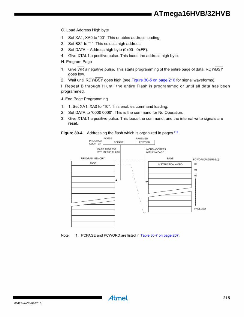
ATmega16HVB/32HVB
G. Load Address High byte
1. Set XA1, XA0 to “00”. This enables address loading.
2. Set BS1 to “1”. This selects high address.
3. Set DATA = Address high byte (0x00 - 0xFF).
4. Give XTAL1 a positive pulse. This loads the address high byte.
H. Program Page
1. Give WR a negative pulse. This starts programming of the entire page of data. RDY/BSY goes low.
2. Wait until RDY/BSY goes high (see Figure 30-5 on page 216 for signal waveforms).
I. Repeat B through H until the entire Flash is programmed or until all data has beenprogrammed.
J. End Page Programming
1. 1. Set XA1, XA0 to “10”. This enables command loading.
2. Set DATA to “0000 0000”. This is the command for No Operation.
3. Give XTAL1 a positive pulse. This loads the command, and the internal write signals are reset.
Figure 30-4. Addressing the flash which is organized in pages (1).
Note: 1. PCPAGE and PCWORD are listed in Table 30-7 on page 207.
PROGRAM MEMORY
WORD ADDRESSWITHIN A PAGE
PAGE ADDRESSWITHIN THE FLASH
INSTRUCTION WORD
PAGE PCWORD[PAGEMSB:0]:
00
01
02
PAGEEND
PAGE
PCWORDPCPAGE
PCMSB PAGEMSBPROGRAMCOUNTER
2158042E–AVR–09/2013

Figure 30-5. Programming the flash waveforms (1).
Note: 1. “XX” is don’t care. The letters refer to the programming description above.
30.7.6 Programming the EEPROM
The EEPROM is organized in pages, see Table 30-8 on page 207. When programming theEEPROM, the program data is latched into a page buffer. This allows one page of data to beprogrammed simultaneously. The programming algorithm for the EEPROM data memory is asfollows (refer to ”Programming the flash” on page 214 for details on Command, Address andData loading):
1. A: Load Command “0001 0001”.
2. G: Load Address High Byte (0x00 - 0xFF).
3. B: Load Address Low Byte (0x00 - 0xFF).
4. C: Load Data (0x00 - 0xFF).
5. E: Latch data (give PAGEL a positive pulse).
K: Repeat 3 through 5 until the entire buffer is filled
L: Program EEPROM page
1. Set BS to “0”.
2. Give WR a negative pulse. This starts programming of the EEPROM page. RDY/BSY goes low.
3. Wait until to RDY/BSY goes high before programming the next page (see Figure 30-6 on page 217 for signal waveforms).
RDY/BSY
WR
OE
RESET +12V
PAGEL
BS2
0x10 ADDR. LOW ADDR. HIGHDATADATA LOW DATA HIGH ADDR. LOW DATA LOW DATA HIGH
XA1
XA0
BS1
XTAL1
XX XX XX
A B C D E B C D E G H
F
2168042E–AVR–09/2013
ATmega16HVB/32HVB
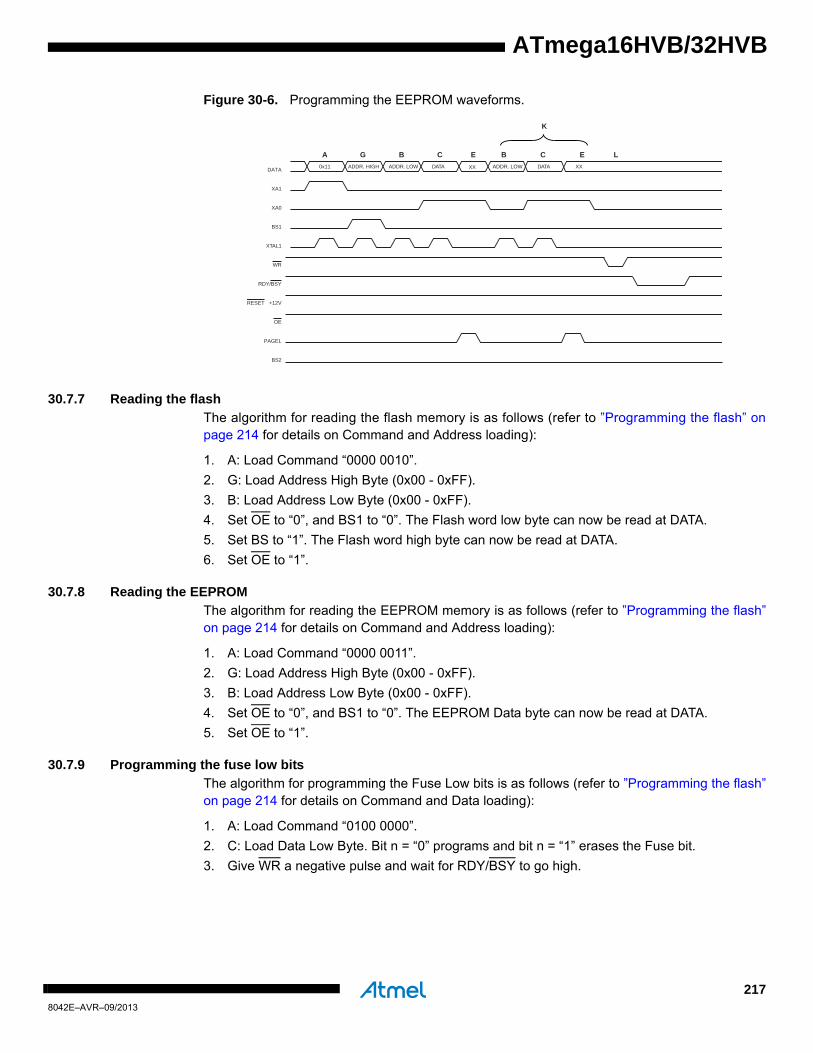
ATmega16HVB/32HVB
Figure 30-6. Programming the EEPROM waveforms.
30.7.7 Reading the flash
The algorithm for reading the flash memory is as follows (refer to ”Programming the flash” onpage 214 for details on Command and Address loading):
1. A: Load Command “0000 0010”.
2. G: Load Address High Byte (0x00 - 0xFF).
3. B: Load Address Low Byte (0x00 - 0xFF).
4. Set OE to “0”, and BS1 to “0”. The Flash word low byte can now be read at DATA.
5. Set BS to “1”. The Flash word high byte can now be read at DATA.
6. Set OE to “1”.
30.7.8 Reading the EEPROM
The algorithm for reading the EEPROM memory is as follows (refer to ”Programming the flash”on page 214 for details on Command and Address loading):
1. A: Load Command “0000 0011”.
2. G: Load Address High Byte (0x00 - 0xFF).
3. B: Load Address Low Byte (0x00 - 0xFF).
4. Set OE to “0”, and BS1 to “0”. The EEPROM Data byte can now be read at DATA.
5. Set OE to “1”.
30.7.9 Programming the fuse low bits
The algorithm for programming the Fuse Low bits is as follows (refer to ”Programming the flash”on page 214 for details on Command and Data loading):
1. A: Load Command “0100 0000”.
2. C: Load Data Low Byte. Bit n = “0” programs and bit n = “1” erases the Fuse bit.
3. Give WR a negative pulse and wait for RDY/BSY to go high.
RDY/BSY
WR
OE
RESET +12V
PAGEL
BS2
0x11 ADDR. HIGHDATA
ADDR. LOW DATA ADDR. LOW DATA XX
XA1
XA0
BS1
XTAL1
XX
A G B C E B C E L
K
2178042E–AVR–09/2013
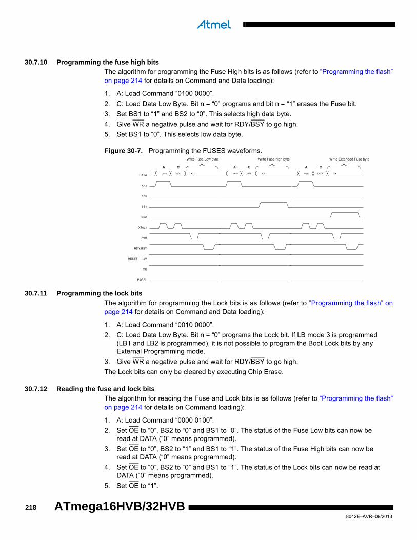
30.7.10 Programming the fuse high bits
The algorithm for programming the Fuse High bits is as follows (refer to ”Programming the flash”on page 214 for details on Command and Data loading):
1. A: Load Command “0100 0000”.
2. C: Load Data Low Byte. Bit n = “0” programs and bit n = “1” erases the Fuse bit.
3. Set BS1 to “1” and BS2 to “0”. This selects high data byte.
4. Give WR a negative pulse and wait for RDY/BSY to go high.
5. Set BS1 to “0”. This selects low data byte.
Figure 30-7. Programming the FUSES waveforms.
30.7.11 Programming the lock bits
The algorithm for programming the Lock bits is as follows (refer to ”Programming the flash” onpage 214 for details on Command and Data loading):
1. A: Load Command “0010 0000”.
2. C: Load Data Low Byte. Bit n = “0” programs the Lock bit. If LB mode 3 is programmed (LB1 and LB2 is programmed), it is not possible to program the Boot Lock bits by any External Programming mode.
3. Give WR a negative pulse and wait for RDY/BSY to go high.
The Lock bits can only be cleared by executing Chip Erase.
30.7.12 Reading the fuse and lock bits
The algorithm for reading the Fuse and Lock bits is as follows (refer to ”Programming the flash”on page 214 for details on Command loading):
1. A: Load Command “0000 0100”.
2. Set OE to “0”, BS2 to “0” and BS1 to “0”. The status of the Fuse Low bits can now be read at DATA (“0” means programmed).
3. Set OE to “0”, BS2 to “1” and BS1 to “1”. The status of the Fuse High bits can now be read at DATA (“0” means programmed).
4. Set OE to “0”, BS2 to “0” and BS1 to “1”. The status of the Lock bits can now be read at DATA (“0” means programmed).
5. Set OE to “1”.
RDY/BSY
WR
OE
RESET +12V
PAGEL
0x40DATA
DATA XX
XA1
XA0
BS1
XTAL1
A C
0x40 DATA XX
A C
Write Fuse Low byte Write Fuse high byte
0x40 DATA XX
A C
Write Extended Fuse byte
BS2
2188042E–AVR–09/2013
ATmega16HVB/32HVB

ATmega16HVB/32HVB
Figure 30-8. Mapping between BS1, BS2 and the fuse and lock bits during read.
30.7.13 Reading the Signature bytes
The algorithm for reading the Signature bytes is as follows (refer to ”Programming the flash” onpage 214 for details on Command and Address loading):
1. A: Load Command “0000 1000”.
2. B: Load Address Low Byte (0x00 - 0x02).
3. Set OE to “0”, and BS to “0”. The selected Signature byte can now be read at DATA.
4. Set OE to “1”.
30.7.14 Reading the Calibration byte
The algorithm for reading the Calibration byte is as follows (refer to ”Programming the flash” onpage 214 for details on Command and Address loading):
1. A: Load Command “0000 1000”.
2. B: Load Address Low Byte, 0x00.
3. Set OE to “0”, and BS1 to “1”. The Calibration byte can now be read at DATA.
4. Set OE to “1”.
Lock Bits 0
1
BS2
Fuse High Byte
0
1
BS1
DATA
Fuse Low Byte 0
1
BS2
Extended Fuse Byte
2198042E–AVR–09/2013
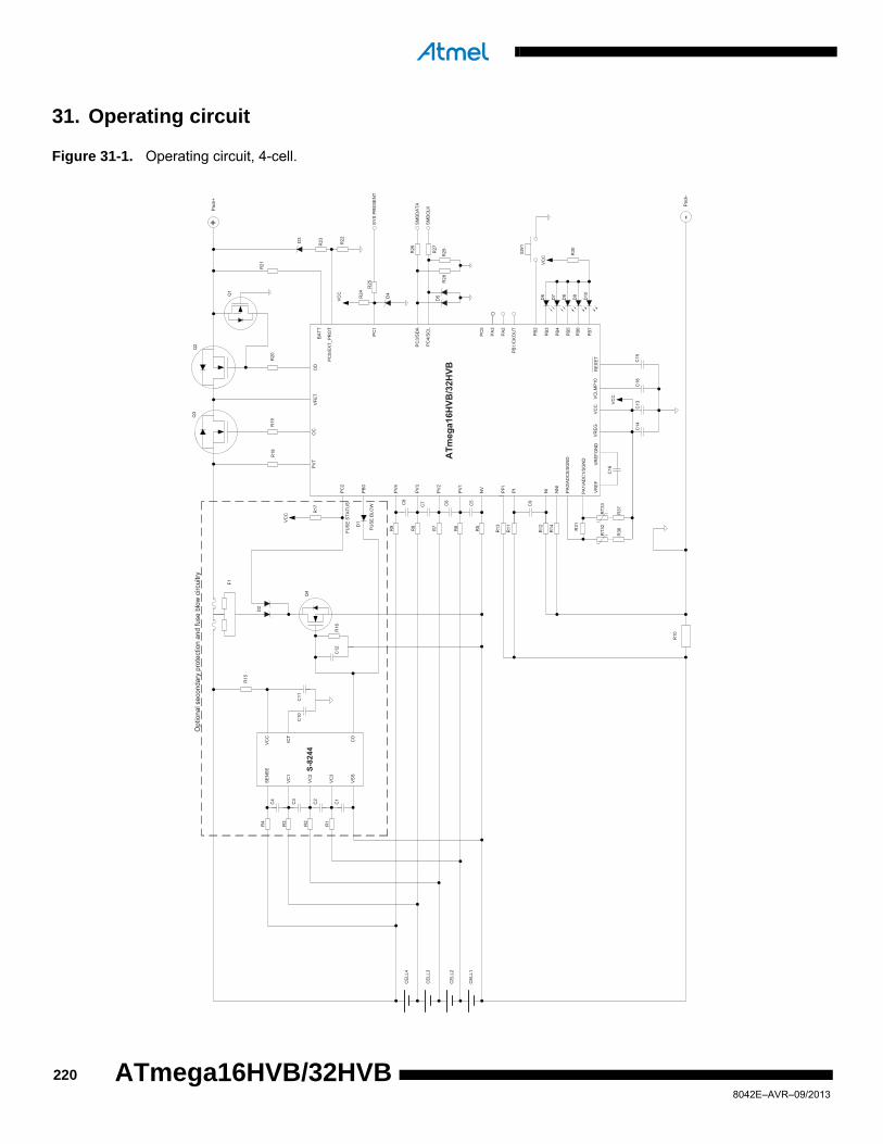
31. Operating circuit
Figure 31-1. Operating circuit, 4-cell.
R8
R6
D
6
D
7
D
8
D
9
D10
ATmega16HVB/32HVB
VFE
TO
CP
VT
OD
+
PV
4
PV
3
PV
2
PV
1
NV
PA
1/AD
C1/
SG
ND
PA
0/A
DC
0/S
GN
D
RE
SE
TV
RE
GPB
7
PB6
PB3
PB4
PB5
BA
TT
R7
VR
EF
VR
EFG
ND
SM
BD
ATA
SM
BC
LK
R28
R29
VC
C
R20
R19
R21
PA
2
PC
5
R27
PB
0
PB
1/C
KO
UT
PB
2
PC
3/S
DA
PC
4/S
CL
PC
0/E
XT_
PR
OT
D3
R22
R23
PC
2
R17
C14
C13
C15
PC
1
C7 C6
C5
R5
C16
C12
SW
1
D4
SY
S P
RE
SE
NT
R24
FUS
E B
LOW
FUS
E S
TATU
S
R25
R26
F1
D1
R16
Q2
Q3
Q4
PA
3
R9
R10
R11
R12
C9
PI
NI
NN
I
PP
IR
13
R14
R18
-
R3
R1
R2
R4
S-8244
R
15
SE
NS
E
VC
1
VC
2
VC
3
VS
S
VC
C
ICT
CO
C8
VC
C
VC
C
VC
C
VC
C
C10
C4
C3
C2
C1
C11
R30
Q1
D2
D5
RT3
3R
T32
CE
LL4
CE
LL3
CE
LL2
CE
LL1
Pack
+
Pack
-
C18
VC
LMP
10
Opt
iona
l sec
onda
ry p
rote
ctio
n an
d fu
se b
low
circ
uitry
R31
R36
R37
2208042E–AVR–09/2013
ATmega16HVB/32HVB

ATmega16HVB/32HVB
Figure 31-2. Operating circuit, 3-cell.
R8
R6
D
6
D
7
D
8
D
9
D10
ATm
ega16HVB/32HVB
VFE
TO
CP
VT
OD
+
PV4
PV3
PV2
PV1
NV
PA
1/A
DC
1/S
GN
D
PA0
/AD
C0/
SG
ND
RE
SET
VRE
GP
B7
PB6
PB3
PB4
PB5
BA
TT
R7
VRE
FV
RE
FGN
D
SM
BD
ATA
SM
BC
LK
R28
R29
VC
C
R20
R19
R21
PA2
PC
5
R27
PB0
PB1
/CK
OU
T
PB
2
PC
3/S
DA
PC4/
SC
L
PC
0/EX
T_P
RO
T
D3
R22
R23
PC
2
R17
C14
C13
C15
PC
1
C6
C5
R5
C12
SW1
D4
SY
S P
RE
SEN
T
R24
FUSE
BLO
W
FUS
E S
TATU
S
R25
R26
F1
D1
R16
Q2
Q3
Q4
PA3
R10
R11
R12
C9
PI
NI
NN
I
PPI
R13
R14
R18
-
R3
R2
R4
S-8244
R
15
SEN
SE
VC
1
VC
2
VC
3
VSS
VCC
ICT
CO
VC
C
VC
C
VCC
VC
C
C10
C4
C3
C2
C11
R30
Q1
D2
D5
CE
LL3
CE
LL2
CE
LL1
Pac
k+
Pack
-
C18
VC
LMP
10
Opt
iona
l sec
onda
ry p
rote
ctio
n an
d fu
se b
low
circ
uitry
R9
C7
C16
RT3
3R
T32
R31
R36
R37
2218042E–AVR–09/2013

Figure 31-3. Operating circuit, 2-cell.
R8
R6
D
6
D
7
D
8
D
9
D10
ATmega16HVB/32HVB
VFE
TO
CPV
TO
D
+
PV4
PV3
PV2
PV1
NV
PA1/
ADC
1/SG
ND
PA0/
AD
C0/
SGN
D
RE
SET
VR
EG
PB7
PB6
PB3
PB4
PB5
BAT
T
R7
VR
EF
VR
EFG
ND
SM
BD
ATA
SMBC
LK
R28
R29
VCC
R20
R19
R21
PA
2
PC5
R27
PB0
PB
1/C
KO
UT
PB2
PC
3/S
DA
PC
4/S
CL
PC0/
EXT_
PRO
T
D3
R22
R23
PC2
R17
C14
C13
C15
PC
1
C6
C5
R5
C12
SW
1
D4
SYS
PR
ESE
NT
R24
FUSE
BLO
W
FUS
E S
TATU
S
R25
R26
F1
D1
R16
Q2
Q3
Q4
PA
3
R10
R11
R12
C9
PI NI
NN
I
PPI
R13
R14
R18
-
R3
R4
S-8244
R
15
SEN
SE
VC1
VC2
VC3
VSS
VCC
ICT
CO
VC
C
VCC
VC
C
VC
C
C10
C4
C3
C11
R30
Q1
D2
D5
CEL
L2
CEL
L1
Pack
+
Pac
k-
C18
VC
LMP1
0
Opt
iona
l sec
onda
ry p
rote
ctio
n an
d fu
se b
low
circ
uitry
R9
Q5
R34
R35
C16
RT3
3R
T32
R31
R36
R37
2228042E–AVR–09/2013
ATmega16HVB/32HVB

ATmega16HVB/32HVB
Table 31-1. Bill of materials.
Symbol Number Description
C1-C4, C10, C11 6 Capacitor, ceramic, 0.1µF - 1.0µF , 50V, X7R
C5-C8 4 Capacitor, ceramic, 0.01µF - 0.5µF, 50V, X7R
C9, C12, C13, C15 4 Capacitor, ceramic, 0.1µF, 50V, X7R
C14 1 Capacitor, ceramic, 2.2µF - 4.7µF, 10V, X7R
C16 1 Capacitor, ceramic, 1µF - 22µF, 10V, X7R
C18 1 Capacitor, ceramic, 22nF, 50V, X7R
D1 1 Diode, signal
D2 1 Diode, double, Shottky
D4 1 Diode, signal
D3 1 Diode, Zener, value from design considerations
D4 1 Diode, Zener, 5V6
D5 1 Diode, double, Zener, 5V6
D6-D10 5 LEDs
F1 1 Chemical fuse
Q1 1 N-FET, 50V, 0.22A
Q2, Q3 2 N-FET, 30V, 10A
Q4 1 N-FET, 20V, 1.3A
Q5 1 P-FET, 30V, 10A
R1-R4 4 Resistor, chip, 1k - 10k, 1/16W, 5%
R5-R9 5 Resistor, chip, 10k - 1000, 1/16W, 5%
R10 1 Sense resistor, 1m - 10m, 1W, 1%
R11, R12 2 Resistor, chip, 10 - 500, 1/16W, 5%
R13, R14, R18, R19, R20, R21, R25 7 Resistor, chip 1k, 1/16W, 5%
R15 1 Resistor, chip, 100 - 1000, 1/16W, 5%
R16, R17 2 Resistor, chip 200k, 1/16W, 5%
R22 1 Resistor, value from design considerations
R23 1 Resistor, value from design considerations
R24 1 Resistor, chip 1k, 1/16W, 5%
R26, R27 2 Resistor, chip 100, 1/16W, 5%
R28, R29 2 Resistor, chip 1M, 1/16W, 5%
R30 1 Resistor, chip 820, 1/16W, 5%
R31 1 Resistor, chip 2.4k, 1/16W, 5%
R32, R33 2 NTC thermistor, 10k, B = 3000 - 4000
R34 1 Resistor, value determined by battery pack and charger requirements
R35 1 Resistor, chip 1M, 1/16W, 5%
2238042E–AVR–09/2013

R36, R37 2 Resistor, chip 5.1k, 1/16W, 5%
SW 1 Switch, push button
U1 1 Atmel ATmega32HVB
U2 1 S-8244 secondary protection device (Seiko Instruments)
Symbol Number Description
2248042E–AVR–09/2013
ATmega16HVB/32HVB

ATmega16HVB/32HVB
32. Electrical characteristics
32.1 Absolute maximum ratings*
32.2 Supply current characteristics
Operating temperature .................................... -40C to +85C *NOTICE: Stresses beyond those listed under “Absolute Maximum Ratings” may cause permanent dam-age to the device. This is a stress rating only and functional operation of the device at these or other conditions beyond those indicated in the operational sections of this specification is not implied. Exposure to absolute maximum rating conditions for extended periods may affect device reliability.
Storage temperature...................................... -65°C to +150°C
Voltage on PA0 - PA3, PI, NI, PPI and NNIwith respect to ground .............................. -0.5V to VREG +0.5V
Voltage on PB0 - PB7with respect to ground .............................. -0.5V to VCC +0.5V
Voltage on PC0 - PC4,PV1, and NV with respect to ground..................-0.5V to +6.0V
Voltage on OC and OD with respect to ground...-0.5V to +35V
Voltage on PC5, BATT, PVT, VFET, PV4, PV3, and PV2with respect to ground ........................................-0.5V to +25V
Voltage on PV4 with respect to PV3: ................. -0.5V to +10V
Voltage on PV3 with respect to PV2: ................. -0.5V to +10V
Voltage on PV2 with respect to PV1: ................. -0.5V to +10V
Voltage on PV1 with respect to NV: ................... -0.5V to +10V
Voltage on PVT with respect to VFET: .............................. 10V
Voltage on VCLMP10 and RESETwith respect to ground ........................................-0.5V to +13V
Maximum operating voltage on VREG and VCC.............. 4.5V
Maximum operating voltage on VFET ............................... 18V
Table 32-1. TA= 25°C unless otherwise noted.
Symbol Parameter Condition Minimum Typical Maximum Units
IVFET
Active currentVFET = 16V, CPU clock = 8MHz, All PRR bits set 3.75 5 mA
VFET = 16V, CPU clock = 1MHz, All PRR bits set 760 1000
µA
Idle current VFET = 16V, CPU clock = 1MHz, All PRR bits set 215 293
ADCNRM currentVFET = 16V, CPU clock = 1MHz, All PRR bits except PRVADC are set, VADC enabled
350
Power-save current
VFET = 16V, Only WDT enabled, DUVR mode disabled
28 46
VFET = 16V, WDT, CC-ADC, OC, OD and Battery Protection enabled, DUVR mode disabled
115 170
Power-off current VFET = 6V <1 2
2258042E–AVR–09/2013
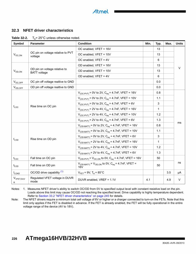
32.3 NFET driver characteristics
Notes: 1. Measures NFET driver’s ability to switch OC/OD from 0V to specified output level with constant resistive load on the pin. Loads above this limit may cause OC/OD not reaching the specified level. Drive capability is highly temperature dependent. Refer to Section 33.2 ”NFET driver characteristics” on page 245 for details.
Note: The NFET drivers require a minimum total cell voltage of 6V or higher or a charger connected to turn-on the FETs. Note that this limit only applies if the FET is disabled in advance. If the FET is already enabled, the FET will be fully operational in the entire voltage range of the device (4V to 18V).
Table 32-2. TA= 25°C unless otherwise noted.
Symbol Parameter Condition Min. Typ. Max. Units
VOC,ONOC pin on voltage relative to PVT voltage
OC enabled, VFET = 16V 13
V
OC enabled, VFET = 10V 13
OC enabled, VFET = 4V 6
VOD,ONOD pin on voltage relative to BATT voltage
OD enabled, VFET = 16V 13
OD enabled, VFET = 10V 13
OD enabled, VFET = 4V 6
VOC,OFF OC pin off voltage realtive to GND 0.0
VOD,OFF OD pin off voltage realtive to GND 0.0
tr,OC Rise time on OC pin
V(OC-PVT) = 0V to 2V, Ceq = 4.7nF, VFET = 16V 0.8
ms
V(OC-PVT) = 0V to 2V, Ceq = 4.7nF, VFET = 10V 1.1
V(OC-PVT) = 0V to 2V, Ceq = 4.7nF, VFET = 6V 3
V(OC-PVT) = 2V to 4V, Ceq = 4.7nF, VFET = 16V 1
V(OC-PVT) = 2V to 4V, Ceq = 4.7nF, VFET = 10V 1.2
V(OC-PVT) = 2V to 4V, Ceq = 4.7nF, VFET = 6V 1.3
tr,OD Rise time on OD pin
V(OD-BATT) = 0V to 2V, Ceq = 4.7nF, VFET = 16V 0.8
V(OD-BATT) = 0V to 2V, Ceq = 4.7nF, VFET = 10V 1.1
V(OD-BATT) = 0V to 2V, Ceq = 4.7nF, VFET = 6V 3
V(OD-BATT) = 2V to 4V, Ceq = 4.7nF, VFET = 16V 1
V(OD-BATT) = 2V to 4V, Ceq = 4.7nF, VFET = 10V 1.2
V(OD-BATT) = 2V to 4V, Ceq = 4.7nF, VFET = 6V 1.3
tf,OC Fall time on OC pin V(OD-PVT) = VOC,ON to 0V, Ceq = 4.7nF, VFET = 16V 50
nstf,OD Fall time on OD pin
V(OD-BATT) = VOD,ON to 0V, Ceq = 4.7nF, VFET = 16V
50
ILOAD OC/OD drive capability (1) VFET = 9V, TA = 85°C 3.5 µA
VVFET,DUV
R
Regulated VFET voltage in DUVR mode
DUVR enabled, VREF = 1.1V 4.1 4.9 V
2268042E–AVR–09/2013
ATmega16HVB/32HVB

ATmega16HVB/32HVB
32.4 Reset characteristics
Notes: 1. The voltage at the pack + terminal will be slightly higher than VPOT when the chip is enabled. This is because of an internal Pull-down current on the BATT pin in the range 50µA - 150µA and the RBATT resistor connected between the Pack + terminal and the BATT pin. RBATT = 1k gives a voltage drop 0.05V - 0.15V.
2. The power-on reset will not work unless the voltage has been below VPOT (falling) after a power-off condition.
32.5 Voltage regulator characteristics
32.6 Voltage reference and temperature sensor characteristics
Notes: 1. Calibration is done in Atmel factory test. Software should calibrate the VREF by writing the BGCRR and BGCCR registers with the calibration values stored in the signature row.
2. This value is not tested in production.3. The measured VPTAT voltage must be scaled with the calibration value stored in the VPTAT Calibration Register to get the
absolute temperature. The design target accuracy for this parameter assumes an exact calibration temperature. Actual accuracy of this parameter after calibration in Atmel factory test remains to be determined.
Table 32-3. TA= -40°C to +85°C unless otherwise noted.
Symbol Parameter Condition Min. Typ. Max. Units
VPOT
Power-on threshold voltage (rising) (1) 4.5 7V
Power-on threshold voltage (falling) (1)(2) 4.5 6.3
tRST Minimum pulse width on RESET Pin 900 ns
VBOT Brown-out detection (BOD) trigger level TA = 25°C 2.9 3.1 V
VHYST BOD level hysteresis TA = 25°C 50 mV
Table 32-4. TA= -40°C to +85°C unless otherwise noted.
Symbol Parameter Condition Min. Typ. Max. Unit
VVREG Regulator output voltage
VFET = 16.8V, IOUT = 20mA 3.1
V
VFET = 6V, IOUT = 20mA 3.1
VFET = 4V, IOUT = 7mA 3.1
VRSCL Voltage regulator short- circuit Level at VFET pin 3.3 3.8
VBLODVoltage Regulator Black-out Detection Level at VREG pin
TA = 25°C 2.65 2.75
Table 32-5. TA= -40°C to +85°C unless otherwise noted.
Parameter Condition Min. Typ. Max. Units
Reference voltage 1.100 V
Reference voltage accuracy (1) After factory calibration,TA = 25°C
±0.1 ±0.2 %
Temperature drift (1)(2)TA = -40C to +85C 60 90
ppm/KTA = 0C to +60C 25 50
VREF calibration
Hold Off Time
CREG = 2.2µF, BGCCR write 2µs
CREG = 2.2µf, BGCRR write 5
VPTAT, voltage proportional to absolute temperature (2) 0.6 mV/K
VPTAT absolute accuracy (3) ±5 K
2278042E–AVR–09/2013

32.7 ADC characteristics
32.7.1 Voltage ADC characteristics
Notes: 1. Value is after Atmel factory offset and gain compensation in production (for details, see Table 29-3, “Signature row address-ing.,” on page 196) and it includes drift over the whole temperature range.
2. Value not tested in production but guaranteed by design and characterization.
Table 32-6. TA= -40°C to +85°C unless otherwise noted.
Parameter Condition Min. Typ. Max. Units
Conversion time clkVADC = 1MHz 519 µs
Resolution 12 Bits
Gain ADC0/1 (un-scaled) 263 µV/LSB
Gain cell inputs (x0.2) 1.42 mV/LSB
INL (2)
ADC0, ADC1 ±1 ±3
LSBCELL1, CELL2, CELL3 ±1 ±3
CELL4 ±2 ±5
Input voltage range ADC0, ADC1, VTEMP 0 1
V
Input voltage range CELL1 1.8 5
Input voltage range CELL2 VPV1-GND>1.8V 0 5
Input voltage range CELL3 VPV2-GND>1.8V 0 5
Input voltage range CELL4 VPV3-GND>1.8V 0 5
Offset drift (1)(2)
ADC0, ADC1 1
LSBCELL1, CELL2, CELL3 1
CELL4 5
Gain drift (1)(2)
ADC0, ADC1 6
LSBCELL1, CELL2, CELL3 7
CELL4 15
2288042E–AVR–09/2013
ATmega16HVB/32HVB
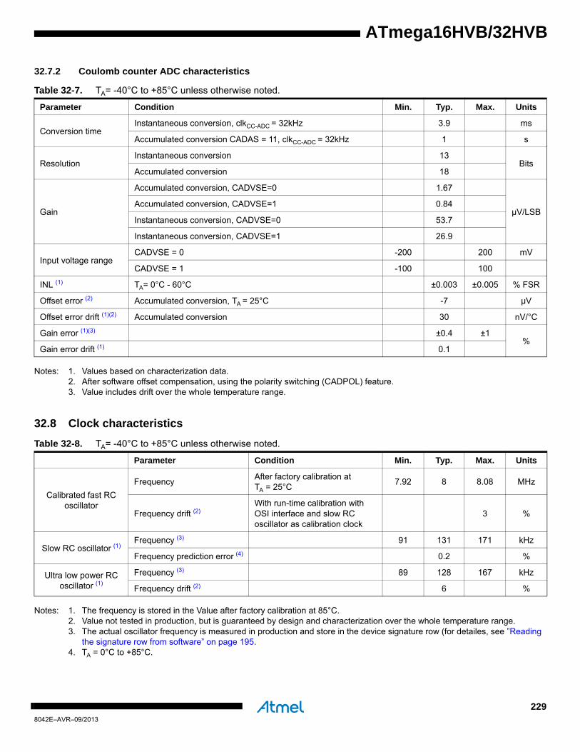
ATmega16HVB/32HVB
32.7.2 Coulomb counter ADC characteristics
Notes: 1. Values based on characterization data.2. After software offset compensation, using the polarity switching (CADPOL) feature.3. Value includes drift over the whole temperature range.
32.8 Clock characteristics
Notes: 1. The frequency is stored in the Value after factory calibration at 85°C.2. Value not tested in production, but is guaranteed by design and characterization over the whole temperature range.3. The actual oscillator frequency is measured in production and store in the device signature row (for detailes, see ”Reading
the signature row from software” on page 195.4. TA = 0°C to +85°C.
Table 32-7. TA= -40°C to +85°C unless otherwise noted.
Parameter Condition Min. Typ. Max. Units
Conversion timeInstantaneous conversion, clkCC-ADC = 32kHz 3.9 ms
Accumulated conversion CADAS = 11, clkCC-ADC = 32kHz 1 s
ResolutionInstantaneous conversion 13
BitsAccumulated conversion 18
Gain
Accumulated conversion, CADVSE=0 1.67
µV/LSBAccumulated conversion, CADVSE=1 0.84
Instantaneous conversion, CADVSE=0 53.7
Instantaneous conversion, CADVSE=1 26.9
Input voltage rangeCADVSE = 0 -200 200 mV
CADVSE = 1 -100 100
INL (1) TA= 0°C - 60°C ±0.003 ±0.005 % FSR
Offset error (2) Accumulated conversion, TA = 25°C -7 µV
Offset error drift (1)(2) Accumulated conversion 30 nV/°C
Gain error (1)(3) ±0.4 ±1%
Gain error drift (1) 0.1
Table 32-8. TA= -40°C to +85°C unless otherwise noted.
Parameter Condition Min. Typ. Max. Units
Calibrated fast RC oscillator
FrequencyAfter factory calibration atTA = 25°C
7.92 8 8.08 MHz
Frequency drift (2)With run-time calibration with OSI interface and slow RC oscillator as calibration clock
3 %
Slow RC oscillator (1)Frequency (3) 91 131 171 kHz
Frequency prediction error (4) 0.2 %
Ultra low power RC oscillator (1)
Frequency (3) 89 128 167 kHz
Frequency drift (2) 6 %
2298042E–AVR–09/2013

32.9 Cell balancing characteristic
32.10 Battery protection characteristics
Notes: 1. Levels in charge and discharge direction can be configured independent of each other.2. VSCD = VNNI - VPPI, VCOCD = VPPI - VNNI, VDOCD = VNNI - VPPI, VCHCD = VPPI - VNNI, VDHCD = VNNI - VPPI
32.11 External interrupt characteristics
Table 32-9. TA= 25°C unless otherwise noted.
Parameter Condition Min. Typ. Max. Unit
Balancing current Battery cell voltage VCELL = 4.2V, V-ADC filter resistance = 470 4 mA
Table 32-10. TA= -40°C to +85°C unless otherwise noted.
Parameter Condition Min. Max. Unit
Short circuit detection level error (1)
Charge/discharge over current detection level error (1)
Charge/discharge high current detection detection level error (1)
VSCD, VCOCD, VDOCD, VCHCD, and VDHCDfrom 20mV to 70mV (2) -10 +10
mV
VSCD, VCOCD, VDOCD, VCHCD, and VDHCDfrom 80mV to 140mV (2) -15 +15
VSCD, VCOCD, VDOCD, VCHCD, and VDHCDfrom 150mV to 270mV (2) -35 +35
VSCD, VCOCD, VDOCD, VCHCD, and VDHCDat 310mV (2) -50 +50
Table 32-11. Asynchronous external interrupt characteristics.
Symbol Parameter Condition Min. Typ. Max. Unit
tINTMinimum pulse width for asynchronous external interrupt
50 ns
2308042E–AVR–09/2013
ATmega16HVB/32HVB

ATmega16HVB/32HVB
32.12 General I/O lines characteristics
32.12.1 Port A and B characteristics
Notes: 1. “Max” means the highest value where the pin is guaranteed to be read as low.2. “Min” means the lowest value where the pin is guaranteed to be read as high.3. Although each I/O port can sink more than the test conditions (5mA at VCC = 3.3V) under steady state conditions (non-tran-
sient), the following must be observed:- The sum of all IOL should not exceed 20mAIf IOL exceeds the test condition, VOL may exceed the related specification. Pins are not guaranteed to sink current greater than the listed test condition.
4. Although each I/O port can source more than the test conditions (2mA at VCC = 3.3V) under steady state conditions (non-transient), the following must be observed:- The sum of all IOH should not exceed 2mAThis restriction is put because the device should be within spec throughout the whole operation range. The integrated volt-age regulator could have problems providing this output when supplying high currents at low VFET voltages.
5. The typical hysteresis on VIL/VIH is 300mV on all PA and PB pins except PA3. PA3 has a typical hysteresis of 50mV.
32.12.2 Port C characteristics
Note: 1. This values is based on characterization and is not tested in production.
Table 32-12. TA = -40°C to +85°C, VCC = 3.3V (unless otherwise noted).
Symbol Parameter Condition Min. Typ. Max. Units
VIL Input low voltage, Except RESET pin -0.5 0.3VCC (1)
V
VIL1 Input low voltage, RESET pin 0.3VCC (1)
VIH Input high voltage, Except RESET pin 0.6VCC (2) VCC + 0.5
VIH1 Input high voltage, RESET pin 0.9VCC (2) VCC + 0.5
VOL Output low voltage IOL = 5mA 0.5
VOH Output high voltage IOH = 2mA 2.3
IIL Input leakage current I/O Pin Pin low (absolute value) 1µA
IIH Input leakage current I/O Pin Pin high (absolute value) 1
RRST Reset pull-up resistor 30 60k
RPU I/O pin pull-up resistor 20 50
Table 32-13. PC0-PC4 characteristics.
Symbol Parameter Condition Min. Max. Unit
VIL Input low-voltage -0.5 0.8
VVIH Input high-voltage 2.1 5.5
VOL (1) Output low-voltage 350µA sink current 0 0.4
Table 32-14. PC5 characteristic.
Symbol Parameter Condition Min. Max. Unit
VOL Output low-voltage 500µA sink current 0 0.2 V
2318042E–AVR–09/2013

32.13 2-wire serial interface characteristicsTable 32-15 describes the requirements for devices connected to the Two-wire Serial Bus. TheAtmel ATmega16HVB/32HVB Two-wire Serial Interface meets or exceeds these requirementsunder the noted conditions.
Timing symbols refer to Figure 32-1 on page 233.
Notes: 1. In ATmega16HVB/32HVB, this parameter is characterized and not tested.2. Cb = capacitance of one bus line in pF.3. fCK = CPU clock frequency.4. This requirement applies to all ATmega16HVB/32HVB Two-wire Serial Interface operation. Other devices connected to the
Two-wire Serial Bus need only obey the general fSCL requirement.
Table 32-15. Two-wire serial bus requirements.
Symbol Parameter Condition Minimum Maximum Units
VIL Input low-voltage -0.5 0.8
VVIH Input high-voltage 2.1 5.5
VOL (1) Output low-voltage 350µA sink current 0 0.4
tr (1) Rise time for both SDA and SCL 300
nstof (1) Output fall time from VIHmin to VILmax Cb < 400pF (2) 250
tSP (1) Spikes suppressed by input filter 0 50
Ii Input current each I/O pin 0.1VBUS < Vi < 0.9VBUS -5 5 µA
Ci (1) Capacitance for each I/O pin – 10 pF
fSCL SCL clock frequency fCK (3) > max(16fSCL, 450Hz) (4) 0 100 kHz
Rp Value of pull-up resistorfSCL 100Hz
tHD;STA Hold time (repeated) START condition fSCL 100kHz 4.0 –
µs
tLOW Low period of the SCL clock fSCL 100kHz 4.7 –
tHIGH High period of the SCL clock fSCL 100kHz 4.0 –
tSU;STA Set-up time for a repeated START condition fSCL 100kHz 4.7 –
tHD;DAT Data hold time fSCL 100kHz 0.3 3.45
tSU;DAT Data setup time fSCL 100kHz 250 –
tSU;STO Setup time for STOP condition fSCL 100kHz 4.0 –
tBUFBus free time between a STOP and START condition
fSCL 100kHz 4.7 –
VBUS 0.4V–
350µA-------------------------------
VBUS 0.4V–
100µA-------------------------------
2328042E–AVR–09/2013
ATmega16HVB/32HVB

ATmega16HVB/32HVB
Figure 32-1. Two-wire serial bus timing.
32.14 SPI timing characteristics
See Figure 32-2 on page 234 and SPI interface timing requirements (Slave mode).234 fordetails.
Note: 1. Refer to ”Serial programming” on page 207 for serial programming requirements.
tSU;STA
tLOW
tHIGH
tLOW
tof
tHD;STA tHD;DAT tSU;DATtSU;STO
tBUF
SCL
SDA
tr
Table 32-16. SPI timing parameters.
Description Mode Minimum Typical Maximum Units
1 SCK period MasterSee Figure 18-5
on page 106
ns
2 SCK high/low Master 50% duty cycle
3 Rise/fall time Master 3.6
4 Setup Master 10
5 Hold Master 10
6 Out to SCK Master 0.5 • tsck
7 SCK to out Master 10
8 SCK to out high Master 10
9 SS low to out Slave 15
10 SCK period Slave 4 • tck + 40ns
11 SCK high/low (1) Slave 2 • tck + 20ns
12 Rise/fall time Slave 1.6 µs
13 Setup Slave 10
ns
14 Hold Slave tck
15 SCK to out Slave 15
16 SCK to SS high Slave 20
17 SS high to tri-state Slave 10
18 SS low to SCK Slave 20
2338042E–AVR–09/2013

Figure 32-2. SPI interface timing requirements (Master mode).
SPI interface timing requirements (Slave mode).
32.15 Serial programming characteristics
Figure 32-3. Serial programming timing.
MOSI(Data Output)
SCK(CPOL = 1)
MISO(Data Input)
SCK(CPOL = 0)
SS
MSB LSB
LSBMSB
...
...
6 1
2 2
34 5
87
MISO(Data Output)
SCK(CPOL = 1)
MOSI(Data Input)
SCK(CPOL = 0)
SS
MSB LSB
LSBMSB
...
...
10
11 11
1213 14
1715
9
X
16
MOSI
MISO
SCK
tOVSH
tSHSL
tSLSHtSHOX
tSLIV
2348042E–AVR–09/2013
ATmega16HVB/32HVB

ATmega16HVB/32HVB
Figure 32-4. Serial programming waveforms.
Note: 1. 2.2 tCLCL for fck < 12MHz, 3 tCLCL for fck >= 12MHz.
32.16 Parallel programming characteristics
Figure 32-5. Parallel programming timing, including some general timing requirements.
MSB
MSB
LSB
LSB
SERIAL CLOCK INPUT(SCK)
SERIAL DATA INPUT (MOSI)
(MISO)
SAMPLE
SERIAL DATA OUTPUT
Table 32-17. Serial programming characteristics, TA = -40C to +85C, VCC = 3.3V (unless otherwise stated).
Symbol Parameter Min. Typ. Max. Units
1/tCLCL Oscillator frequency (the Atmel ATmega16HVB/32HVB) 0 8 MHz
tCLCL Oscillator period (ATmega16HVB/32HVB) 125
ns
tSHSL SCK pulse width high 2.2 tCLCL (1)
tSLSH SCK pulse width low 2.2 tCLCL (1)
tOVSH MOSI setup to SCK high tCLCL
tSHOX MOSI Hold after SCK High 2 tCLCL
tSLIV SCK Low to MISO Valid 15
Data & Contol(DATA, XA0/1, BS1, BS2)
XTAL1tXHXL
tWLWH
tDVXH tXLDX
tPLWL
tWLRH
WR
RDY/BSY
PAGEL tPHPL
tPLBXtBVPH
tXLWL
tWLBXtBVWL
WLRL
2358042E–AVR–09/2013

Figure 32-6. Parallel programming timing, loading sequence with timing requirements(1).
Note: 1. The timing requirements shown in Figure 32-5 on page 235 (that is, tDVXH, tXHXL, and tXLDX) also apply to loading operation.
Figure 32-7. Parallel programming timing, reading sequence (within the same page) with tim-ing requirements (1).
Note: 1. The timing requirements shown in Figure 32-5 on page 235 (that is, tDVXH, tXHXL, and tXLDX) also apply to reading operation.
Table 32-18. Parallel programming characteristics.
Symbol Parameter Min. Typ. Max. Units
VPP Programming enable voltage (RESET input) 11.5 12.5 V
IPP Programming enable current 250 A
tDVXH Data and control valid before XTAL1 high 67
nstXLXH XTAL1 low to XTAL1 high 200
tXHXL XTAL1 pulse Width high 150
tXLDX Data and control hold after XTAL1 low 67
XTAL1
PAGEL
tPLXHXLXHt tXLPH
ADDR0 (Low Byte) DATA (Low Byte) DATA (High Byte) ADDR1 (Low Byte)DATA
BS1
XA0
XA1
LOAD ADDRESS(LOW BYTE)
LOAD DATA (LOW BYTE)
LOAD DATA(HIGH BYTE)
LOAD DATA LOAD ADDRESS(LOW BYTE)
XTAL1
OE
ADDR0 (Low Byte) DATA (Low Byte) DATA (High Byte) ADDR1 (Low Byte)DATA
BS1
XA0
XA1
LOAD ADDRESS(LOW BYTE)
READ DATA (LOW BYTE)
READ DATA(HIGH BYTE)
LOAD ADDRESS(LOW BYTE)
tBVDV
tOLDV
tXLOL
tOHDZ
2368042E–AVR–09/2013
ATmega16HVB/32HVB

ATmega16HVB/32HVB
Notes: 1. tWLRH is valid for the Write Flash, Write Fuse bits and Write Lock bits commands.2. is valid for the Write EEPROM command.3. tWLRH_CE is valid for the Chip Erase command.
tXLWL XTAL1 low to WR low 0
ns
tXLPH XTAL1 low to PAGEL high 0
tPLXH PAGEL low to XTAL1 high 150
tBVPH BS1 valid before PAGEL high 67
tPHPL PAGEL pulse width high 150
tPLBX BS1 hold after PAGEL low 67
tWLBX
BS2/1 hold after WR low. (Fuse programming) 3200
BS2/1 hold after WR low. (All other operations) 67
tPLWL PAGEL low to WR low 67
tBVWL BS1 valid to WR low 67
tWLWH WR pulse Width low 150
tWLRL WR low to RDY/BSY low 0 1 µs
tWLRH WR low to RDY/BSY high (1) 3.7 4.5
mstWLRH_EE WR low to RDY/BSY high (2) 2.8 3.6
tWLRH_CE WR low to RDY/BSY high for chip erase (3) 7.5 9.1
tXLOL XTAL1 low to OE low 0
nstBVDV BS1 valid to DATA valid 0 250
tOLDV OE low to DATA Valid 250
tOHDZ OE high to DATA Tri-stated 250
Table 32-18. Parallel programming characteristics. (Continued)
Symbol Parameter Min. Typ. Max. Units
2378042E–AVR–09/2013

33. Typical characteristics
All Typical Characteristics contained in this data sheet are based on characterization of theAtmel ATmega16/32HVB.
33.1 Supply current characteristics
33.1.1 Active supply current characteristics
Active mode current measurements with all bits in the PRR registers set and all I/O modulesturned off.
Figure 33-1. Active supply current vs. VVFET, internal RC oscillator, 8MHz.
85°C
25°C
-40°C
3.6
3.65
3.7
3.75
3.8
3.85
3.9
3.95
4
4 6 8 10 12 14 16 18 20
VVFET [V]
I
[mA
]V
FE
T
2388042E–AVR–09/2013
ATmega16HVB/32HVB
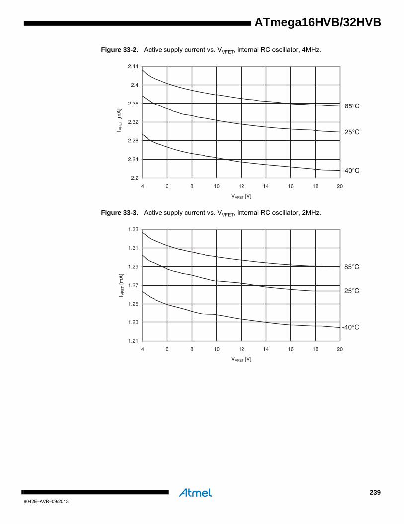
ATmega16HVB/32HVB
Figure 33-2. Active supply current vs. VVFET, internal RC oscillator, 4MHz.
Figure 33-3. Active supply current vs. VVFET, internal RC oscillator, 2MHz.
85°C
25°C
-40°C2.2
2.24
2.28
2.32
2.36
2.4
2.44
4 6 8 10 12 14 16 18 20
VVFET [V]
I
[mA
]V
FE
T
85°C
25°C
-40°C
1.21
1.23
1.25
1.27
1.29
1.31
1.33
4 6 8 10 12 14 16 18 20
VVFET [V]
I
[mA
]V
FE
T
2398042E–AVR–09/2013
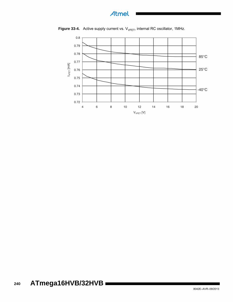
Figure 33-4. Active supply current vs. VVFET, internal RC oscillator, 1MHz.
85°C
25°C
-40°C
0.72
0.73
0.74
0.75
0.76
0.77
0.78
0.79
0.8
4 6 8 10 12 14 16 18 20
VVFET [V]
I
[mA
]V
FE
T
2408042E–AVR–09/2013
ATmega16HVB/32HVB

ATmega16HVB/32HVB
33.1.2 Idle supply current characteristics
Idle current consumption measurements with all bits in the PRR registers set and all I/O modulesare turned off.
Figure 33-5. Idle supply current vs. VVFET, internal RC oscillator, 8MHz.
Figure 33-6. Idle supply current vs. VVFET, internal RC oscillator, 4MHz.
85°C
25°C
-40°C
0.675
0.695
0.715
0.735
0.755
0.775
0.795
0.815
4 6 8 10 12 14 16 18 20
VVFET [V]
I
[mA
]V
FE
T
85°C
25°C
-40°C
0.42
0.43
0.44
0.45
0.46
0.47
0.48
4 6 8 10 12 14 16 18 20
VVFET [V]
I
[mA
]V
FE
T
2418042E–AVR–09/2013

Figure 33-7. Idle supply current vs. VVFET, internal RC oscillator, 2MHz.
Figure 33-8. Idle supply current vs. VVFET, internal RC oscillator, 1MHz.
85°C
25°C
-40°C
0.28
0.284
0.288
0.292
0.296
0.3
0.304
0.308
4 6 8 10 12 14 16 18 20
VVFET [V]
I
[mA
]V
FE
T
85°C
25°C
-40°C
0.205
0.209
0.213
0.217
0.221
0.225
4 6 8 10 12 14 16 18 20
VVFET [V]
I
[mA
]V
FE
T
2428042E–AVR–09/2013
ATmega16HVB/32HVB

ATmega16HVB/32HVB
33.1.3 Power-save current characteristics
Power-save current consumption with External Interrupt and SMBus connect/disconnect func-tionality enabled. The Watchdog Timer, CC-ADC, Current Battery Protection (CBP), VREF, andOC/OD are disabled.
Figure 33-9. Power-save supply current vs. VVFET, external interrupt and SMBus enabled, all other modules disabled.
Table 33-1 shows additional current consumption that needs to be added to the total power-bud-get when additional modules are enableds.
Note: 1. Default I/O register configuration used. PPI and NNI connected to GND.
2. Measurements done with Fairchild FDS6690A N-Channel MOSFET.
Figure 33-11 on page 245 shows Power-Save current consumption vs VFET with all moduleslisted in Table 33-1 enabled. The increased power consumption for low VFET voltage is causedby the NFET driver operation described in Section 25.3 ”Operation and usage” on page 146.
Table 33-1. Typical additional I/O modules current consumption in power-save.
I/O modules enabled Typical current consumption
WDT VREF CBP (1) OC/OD (2) CC-ADC (TA = 25°C and VVFET = 12V)
X 0.8µA
X X 12µA
X X X X 41µA
X X X X X 85µA
85°C
25°C-40°C
17
19
21
23
25
27
29
31
33
35
4 6 8 10 12 14 16 18 20
VVFET [V]
I
[µA
]V
FE
T
2438042E–AVR–09/2013

Figure 33-10. Power-save supply current vs. VVFET, WDT, VREF, CBP, OC/OD, and CC-ADC enabled.
100
120
140
160
180
200
220
240
4 6 8 10 12 14 16 18
VFET [V]
85°C 25°C-40°C
I
[µ
A]
VF
ET
2448042E–AVR–09/2013
ATmega16HVB/32HVB
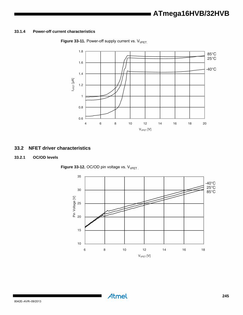
ATmega16HVB/32HVB
33.1.4 Power-off current characteristics
Figure 33-11. Power-off supply current vs. VVFET.
33.2 NFET driver characteristics
33.2.1 OC/OD levels
Figure 33-12. OC/OD pin voltage vs. VVFET .
85°C25°C
-40°C
0.6
0.8
1
1.2
1.4
1.6
1.8
4 6 8 10 12 14 16 18 20
VVFET [V]
I
[µA
]V
FE
T
85°C25°C
-40°C
6 8 10 12 14 16 18
VVFET [V]
10
15
20
25
30
35
Pin
Vol
tage
[V]
2458042E–AVR–09/2013

33.2.2 OC/OD rise time from 0V to 2V gate-source voltage with 4.7nF load
Figure 33-13. OC/OD rise time, VGS = 0V to 2V vs. VVFET .
33.2.3 OC/OD rise time from 2V to 4V gate-source voltage with 4.7nF load
Figure 33-14. OC/OD rise time, VGS = 2V to 4V vs. VVFET .
0
200
400
600
800
1000
1200
1400
1600
1800
6 8 10 12 14 16 18
VFET [V]
Tim
e [µ
s]
T =25°C
T =70°C
0
200
400
600
800
1000
1200
1400
1600
6 8 10 12 14 16 18
VFET [V]
Tim
e [µ
s] T =25°C
T =70°C
2468042E–AVR–09/2013
ATmega16HVB/32HVB

ATmega16HVB/32HVB
Figure 33-15. OC/OD drive capability vs temperature.
3
3.5
4
4.5
5
5.5
6
6.5
7
7.5
8
-10 10 30 50 70 90
Temperature [°C]
Max
Loa
d [µ
A]
VFET = 12VVFET = 9.5VVFET = 6V
2478042E–AVR–09/2013

33.3 Battery protection characteristics
Figure 33-16. Battery protection level.
33.4 Clock characteristics
33.4.1 Fast RC oscillator characteristics
Figure 33-17. Fast RC oscillator frequency vs. temperature (after factory calibration).
10
60
110
160
210
260
310
[m
V]
Det
ectio
n Le
vel
Max
TYP(25°C)
F3 F4 F5 F6 F7 F8 F9 FA FB FC FD 77 78 79 7A 7B 7C 7D 37 38 39 3A 3B 3C 3D 17
Min
Register Value
7.75
7.8
7.85
7.9
7.95
8
8.05
8.1
-40 -30 -20 -10 0 10 20 30 40 50 60 70 80 90
Temperature [°C]
[M
Hz]
Fre
quen
cy
2488042E–AVR–09/2013
ATmega16HVB/32HVB
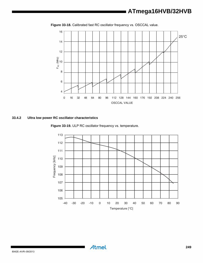
ATmega16HVB/32HVB
Figure 33-18. Calibrated fast RC oscillator frequency vs. OSCCAL value.
33.4.2 Ultra low power RC oscillator characteristics
Figure 33-19. ULP RC oscillator frequency vs. temperature.
25°C
16
14
12
10
8
6
4
0 16 32 48 64 80 96 112 128 144 160 176 192 208 224 240 256
OSCCAL VALUE
FR
C (
MH
z)
105
106
107
108
109
110
111
112
113
-40 -30 -20 -10 0 10 20 30 40 50 60 70 80 90
Temperature [°C]
Fre
quen
cy [k
Hz]
2498042E–AVR–09/2013
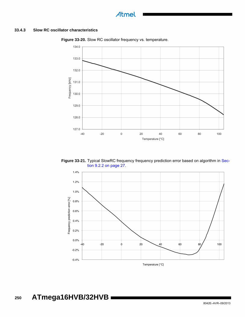
33.4.3 Slow RC oscillator characteristics
Figure 33-20. Slow RC oscillator frequency vs. temperature.
Figure 33-21. Typical SlowRC frequency frequency prediction error based on algorithm in Sec-tion 9.2.2 on page 27.
127.0
128.0
129.0
130.0
131.0
132.0
133.0
134.0
Temperature [°C]
Freq
uenc
y [k
Hz]
-40 -20 0 20 40 60 80 100
-0.4%
-0.2%
0.0%
0.2%
0.4%
0.6%
0.8%
1.0%
1.2%
1.4%
-40 -20 0 20 40 60 80 100
Temperature [°C]
Fre
quen
cy p
redi
ctio
n er
ror
[%]
2508042E–AVR–09/2013
ATmega16HVB/32HVB
ATmega16HVB/32HVB
33.5 Voltage reference characteristics
Figure 33-22. Typical VREF curve with Atmel factory calibration at 25°C and 85°C.
Figure 33-23. Typical VREF deviation curve with Atmel factory calibration at 25°C and 85°C.
Temperature [°C]
-40 -20 0 20 40 60 80
1.091
1.092
1.093
1.094
1.095
1.096
1.097
1.098
1.099
1.100
1.101
VR
EF [V
]
2518042E–AVR–09/2013

33.6 Voltage regulator characteristics
Figure 33-24. Voltage regulator vs. VVFET, ILOAD = 10mA.
Figure 33-25. Voltage regulator vs. VVFET, ILOAD = 20mA.
85°C25°C
-40°C
3.21
3.22
3.23
3.24
3.25
3.26
3.27
4 6 8 10 12 14 16 18 20 22 24 26
VVFET [V]
VR
EG [V
]
85°C25°C
-40°C
2.4
2.5
2.6
2.7
2.8
2.9
3
3.1
3.2
3.3
4 6 8 10 12 14 16 18 20 22 24 26
VVFET [V]
VR
EG [V
]
2528042E–AVR–09/2013
ATmega16HVB/32HVB
ATmega16HVB/32HVB
Figure 33-26. Voltage regulator short-circuit level at VVFET pin vs. temperature.
Figure 33-27. BLOD level.
3.45
3.5
3.55
3.6
3.65
3.7
3.75
-40 -30 -20 -10 0 10 20 30 40 50 60 70 80 90
Temperature [°C]
VR
SC
L [V
]
Rising
Falling
2.637
2.639
2.641
2.643
2.645
2.647
2.649
2.651
2.653
2.655
2.657
2.659
2.661
-40 -30 -20 -10 0 10 20 30 40 50 60 70 80 90
Temperature [°C]
VB
LOD
[V
]
2538042E–AVR–09/2013
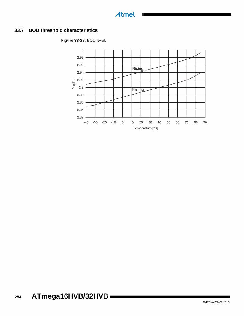
33.7 BOD threshold characteristics
Figure 33-28. BOD level.
Falling
Rising
2.82
2.84
2.86
2.88
2.9
2.92
2.94
2.96
2.98
3
-40 -30 -20 -10 0 10 20 30 40 50 60 70 80 90
Temperature [°C]
VC
C [V
]
2548042E–AVR–09/2013
ATmega16HVB/32HVB
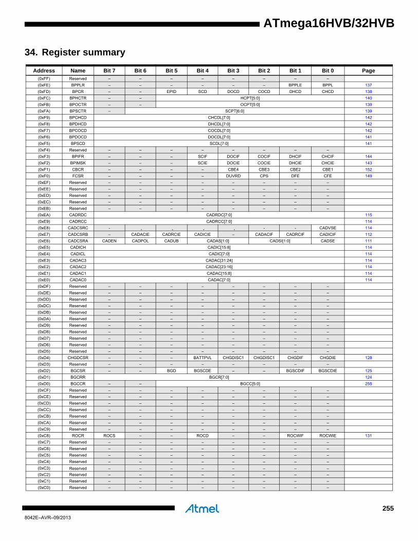
ATmega16HVB/32HVB
34. Register summary
Address Name Bit 7 Bit 6 Bit 5 Bit 4 Bit 3 Bit 2 Bit 1 Bit 0 Page(0xFF) Reserved – – – – – – – –
(0xFE) BPPLR – – – – – – BPPLE BPPL 137
(0xFD) BPCR – – EPID SCD DOCD COCD DHCD CHCD 138
(0xFC) BPHCTR – – HCPT[5:0] 140
(0xFB) BPOCTR – – OCPT[5:0] 139
(0xFA) BPSCTR – SCPT[6:0] 139
(0xF9) BPCHCD CHCDL[7:0] 142
(0xF8) BPDHCD DHCDL[7:0] 142
(0xF7) BPCOCD COCDL[7:0] 142
(0xF6) BPDOCD DOCDL[7:0] 141
(0xF5) BPSCD SCDL[7:0] 141
(0xF4) Reserved – – – – – – – –
(0xF3) BPIFR – – – SCIF DOCIF COCIF DHCIF CHCIF 144
(0xF2) BPIMSK – – – SCIE DOCIE COCIE DHCIE CHCIE 143
(0xF1) CBCR – – – – CBE4 CBE3 CBE2 CBE1 152
(0xF0) FCSR – – – – DUVRD CPS DFE CFE 149
(0xEF) Reserved – – – – – – – –
(0xEE) Reserved – – – – – – – –
(0xED) Reserved – – – – – – – –
(0xEC) Reserved – – – – – – – –
(0xEB) Reserved – – – – – – – –
(0xEA) CADRDC CADRDC[7:0] 115
(0xE9) CADRCC CADRCC[7:0] 114
(0xE8) CADCSRC - - - - - - - CADVSE 114
(0xE7) CADCSRB – CADACIE CADRCIE CADICIE – CADACIF CADRCIF CADICIF 112
(0xE6) CADCSRA CADEN CADPOL CADUB CADAS[1:0] CADSI[1:0] CADSE 111
(0xE5) CADICH CADIC[15:8] 114
(0xE4) CADICL CADIC[7:0] 114
(0xE3) CADAC3 CADAC[31:24] 114
(0xE2) CADAC2 CADAC[23:16] 114
(0xE1) CADAC1 CADAC[15:8] 114
(0xE0) CADAC0 CADAC[7:0] 114
(0xDF) Reserved – – – – – – – –
(0xDE) Reserved – – – – – – – –
(0xDD) Reserved – – – – – – – –
(0xDC) Reserved – – – – – – – –
(0xDB) Reserved – – – – – – – –
(0xDA) Reserved – – – – – – – –
(0xD9) Reserved – – – – – – – –
(0xD8) Reserved – – – – – – – –
(0xD7) Reserved – – – – – – – –
(0xD6) Reserved – – – – – – – –
(0xD5) Reserved – – – – – – – –
(0xD4) CHGDCSR – – – BATTPVL CHGDISC1 CHGDISC1 CHGDIF CHGDIE 128
(0xD3) Reserved – – – – – – – –
(0xD2) BGCSR – – BGD BGSCDE – – BGSCDIF BGSCDIE 125
(0xD1) BGCRR BGCR[7:0] 124
(0xD0) BGCCR – – BGCC[5:0] 255
(0xCF) Reserved – – – – – – – –
(0xCE) Reserved – – – – – – – –
(0xCD) Reserved – – – – – – – –
(0xCC) Reserved – – – – – – – –
(0xCB) Reserved – – – – – – – –
(0xCA) Reserved – – – – – – – –
(0xC9) Reserved – – – – – – – –
(0xC8) ROCR ROCS – – ROCD – – ROCWIF ROCWIE 131
(0xC7) Reserved – – – – – – – –
(0xC6) Reserved – – – – – – – –
(0xC5) Reserved – – – – – – – –
(0xC4) Reserved – – – – – – – –
(0xC3) Reserved – – – – – – – –
(0xC2) Reserved – – – – – – – –
(0xC1) Reserved – – – – – – – –
(0xC0) Reserved – – – – – – – –
2558042E–AVR–09/2013

(0xBF) Reserved – – – – – – – –
(0xBE) TWBCSR TWBCIF TWBCIE – – – TWBDT1 TWBDT0 TWBCIP 184
(0xBD) TWAMR TWAM[6:0] – 184
(0xBC) TWCR TWINT TWEA TWSTA TWSTO TWWC TWEN – TWIE 181
(0xBB) TWDR 2–wire Serial Interface Data Register 183
(0xBA) TWAR TWA[6:0] TWGCE 183
(0xB9) TWSR TWS[7:3] – TWPS1 TWPS0 182
(0xB8) TWBR 2–wire Serial Interface Bit Rate Register 181
(0xB7) Reserved – – – – – – –
(0xB6) Reserved – – – – – – – –
(0xB5) Reserved – – – – – – – –
(0xB4) Reserved – – – – – – – –
(0xB3) Reserved – – – – – – – –
(0xB2) Reserved – – – – – – – –
(0xB1) Reserved – – – – – – – –
(0xB0) Reserved – – – – – – – –
(0xAF) Reserved – – – – – – – –
(0xAE) Reserved – – – – – – – –
(0xAD) Reserved – – – – – – – –
(0xAC) Reserved – – – – – – – –
(0xAB) Reserved – – – – – – – –
(0xAA) Reserved – – – – – – – –
(0xA9) Reserved – – – – – – – –
(0xA8) Reserved – – – – – – – –
(0xA7) Reserved – – – – – – – –
(0xA6) Reserved – – – – – – – –
(0xA5) Reserved – – – – – – – –
(0xA4) Reserved – – – – – – – –
(0xA3) Reserved – – – – – – – –
(0xA2) Reserved – – – – – – – –
(0xA1) Reserved – – – – – – – –
(0xA0) Reserved – – – – – – – –
(0x9F) Reserved – – – – – – – –
(0x9E) Reserved – – – – – – – –
(0x9D) Reserved – – – – – – – –
(0x9C) Reserved – – – – – – – –
(0x9B) Reserved – – – – – – – –
(0x9A) Reserved – – – – – – – –
(0x99) Reserved – – – – – – – –
(0x98) Reserved – – – – – – – –
(0x97) Reserved – – – – – – – –
(0x96) Reserved – – – – – – – –
(0x95) Reserved – – – – – – – –
(0x94) Reserved – – – – – – – –
(0x93) Reserved – – – – – – – –
(0x92) Reserved – – – – – – – –
(0x91) Reserved – – – – – – – –
(0x90) Reserved – – – – – – – –
(0x8F) Reserved – – – – – – – –
(0x8E) Reserved – – – – – – – –
(0x8D) Reserved – – – – – – – –
(0x8C) Reserved – – – – – – – –
(0x8B) Reserved – – – – – – – –
(0x8A) Reserved – – – – – – – –
(0x89) OCR1B Timer/Counter1 – Output Compare Register B 95
(0x88) OCR1A Timer/Counter1 – Output Compare Register A 95
(0x87) Reserved – – – – – – – –
(0x86) Reserved – – – – – – – –
(0x85) TCNT1H Timer/Counter1 (8 Bit) High Byte 95
(0x84) TCNT1L Timer/Counter1 (8 Bit) Low Byte 95
(0x83) Reserved – – – – – – – –
(0x82) Reserved – – – – – – – –
(0x81) TCCR1B – – – – – CS12 CS11 CS10 81
(0x80) TCCR1A TCW1 ICEN1 ICNC1 ICES1 ICS1 – – WGM10 94
(0x7F) Reserved – – – – – – – –
(0x7E) DIDR0 – – – – – – PA1DID PA0DID 121
Address Name Bit 7 Bit 6 Bit 5 Bit 4 Bit 3 Bit 2 Bit 1 Bit 0 Page
2568042E–AVR–09/2013
ATmega16HVB/32HVB
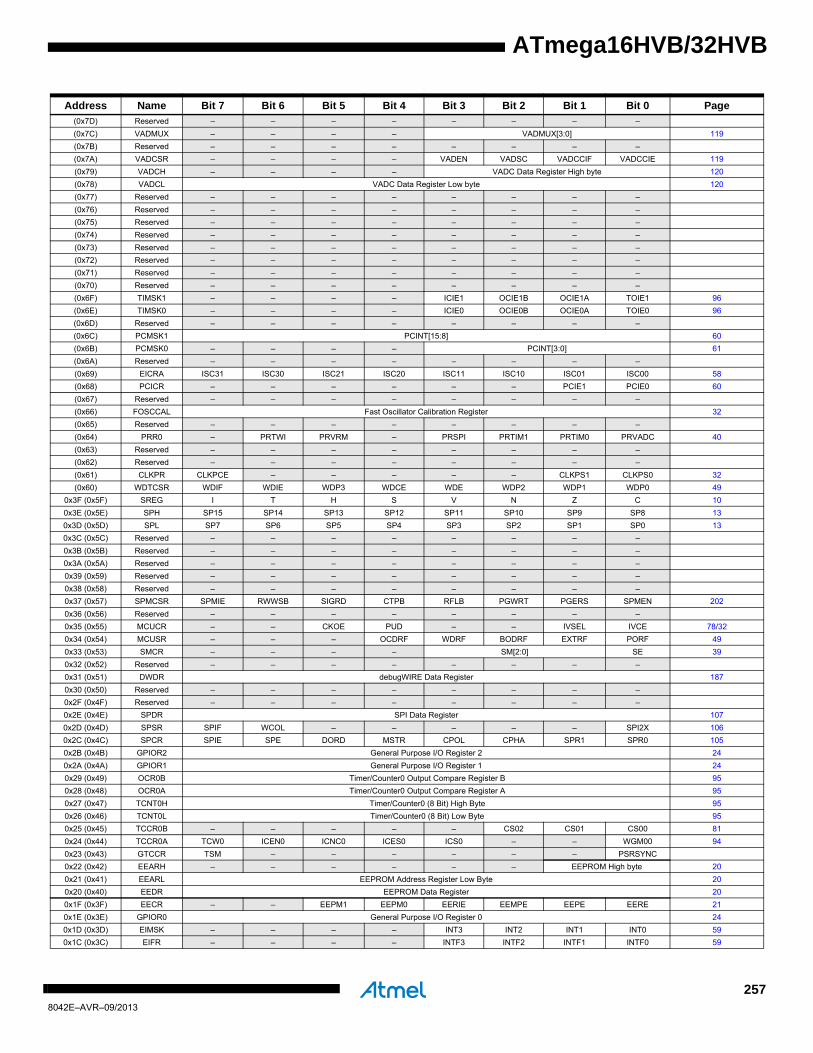
ATmega16HVB/32HVB
(0x7D) Reserved – – – – – – – –
(0x7C) VADMUX – – – – VADMUX[3:0] 119
(0x7B) Reserved – – – – – – – –
(0x7A) VADCSR – – – – VADEN VADSC VADCCIF VADCCIE 119
(0x79) VADCH – – – – VADC Data Register High byte 120
(0x78) VADCL VADC Data Register Low byte 120
(0x77) Reserved – – – – – – – –
(0x76) Reserved – – – – – – – –
(0x75) Reserved – – – – – – – –
(0x74) Reserved – – – – – – – –
(0x73) Reserved – – – – – – – –
(0x72) Reserved – – – – – – – –
(0x71) Reserved – – – – – – – –
(0x70) Reserved – – – – – – – –
(0x6F) TIMSK1 – – – – ICIE1 OCIE1B OCIE1A TOIE1 96
(0x6E) TIMSK0 – – – – ICIE0 OCIE0B OCIE0A TOIE0 96
(0x6D) Reserved – – – – – – – –
(0x6C) PCMSK1 PCINT[15:8] 60
(0x6B) PCMSK0 – – – – PCINT[3:0] 61
(0x6A) Reserved – – – – – – – –
(0x69) EICRA ISC31 ISC30 ISC21 ISC20 ISC11 ISC10 ISC01 ISC00 58
(0x68) PCICR – – – – – – PCIE1 PCIE0 60
(0x67) Reserved – – – – – – – –
(0x66) FOSCCAL Fast Oscillator Calibration Register 32
(0x65) Reserved – – – – – – – –
(0x64) PRR0 – PRTWI PRVRM – PRSPI PRTIM1 PRTIM0 PRVADC 40
(0x63) Reserved – – – – – – – –
(0x62) Reserved – – – – – – – –
(0x61) CLKPR CLKPCE – – – – – CLKPS1 CLKPS0 32
(0x60) WDTCSR WDIF WDIE WDP3 WDCE WDE WDP2 WDP1 WDP0 49
0x3F (0x5F) SREG I T H S V N Z C 10
0x3E (0x5E) SPH SP15 SP14 SP13 SP12 SP11 SP10 SP9 SP8 13
0x3D (0x5D) SPL SP7 SP6 SP5 SP4 SP3 SP2 SP1 SP0 13
0x3C (0x5C) Reserved – – – – – – – –
0x3B (0x5B) Reserved – – – – – – – –
0x3A (0x5A) Reserved – – – – – – – –
0x39 (0x59) Reserved – – – – – – – –
0x38 (0x58) Reserved – – – – – – – –
0x37 (0x57) SPMCSR SPMIE RWWSB SIGRD CTPB RFLB PGWRT PGERS SPMEN 202
0x36 (0x56) Reserved – – – – – – – –
0x35 (0x55) MCUCR – – CKOE PUD – – IVSEL IVCE 78/32
0x34 (0x54) MCUSR – – – OCDRF WDRF BODRF EXTRF PORF 49
0x33 (0x53) SMCR – – – – SM[2:0] SE 39
0x32 (0x52) Reserved – – – – – – – –
0x31 (0x51) DWDR debugWIRE Data Register 187
0x30 (0x50) Reserved – – – – – – – –
0x2F (0x4F) Reserved – – – – – – – –
0x2E (0x4E) SPDR SPI Data Register 107
0x2D (0x4D) SPSR SPIF WCOL – – – – – SPI2X 106
0x2C (0x4C) SPCR SPIE SPE DORD MSTR CPOL CPHA SPR1 SPR0 105
0x2B (0x4B) GPIOR2 General Purpose I/O Register 2 24
0x2A (0x4A) GPIOR1 General Purpose I/O Register 1 24
0x29 (0x49) OCR0B Timer/Counter0 Output Compare Register B 95
0x28 (0x48) OCR0A Timer/Counter0 Output Compare Register A 95
0x27 (0x47) TCNT0H Timer/Counter0 (8 Bit) High Byte 95
0x26 (0x46) TCNT0L Timer/Counter0 (8 Bit) Low Byte 95
0x25 (0x45) TCCR0B – – – – – CS02 CS01 CS00 81
0x24 (0x44) TCCR0A TCW0 ICEN0 ICNC0 ICES0 ICS0 – – WGM00 94
0x23 (0x43) GTCCR TSM – – – – – – PSRSYNC
0x22 (0x42) EEARH – – – – – – EEPROM High byte 20
0x21 (0x41) EEARL EEPROM Address Register Low Byte 20
0x20 (0x40) EEDR EEPROM Data Register 20
0x1F (0x3F) EECR – – EEPM1 EEPM0 EERIE EEMPE EEPE EERE 21
0x1E (0x3E) GPIOR0 General Purpose I/O Register 0 24
0x1D (0x3D) EIMSK – – – – INT3 INT2 INT1 INT0 59
0x1C (0x3C) EIFR – – – – INTF3 INTF2 INTF1 INTF0 59
Address Name Bit 7 Bit 6 Bit 5 Bit 4 Bit 3 Bit 2 Bit 1 Bit 0 Page
2578042E–AVR–09/2013
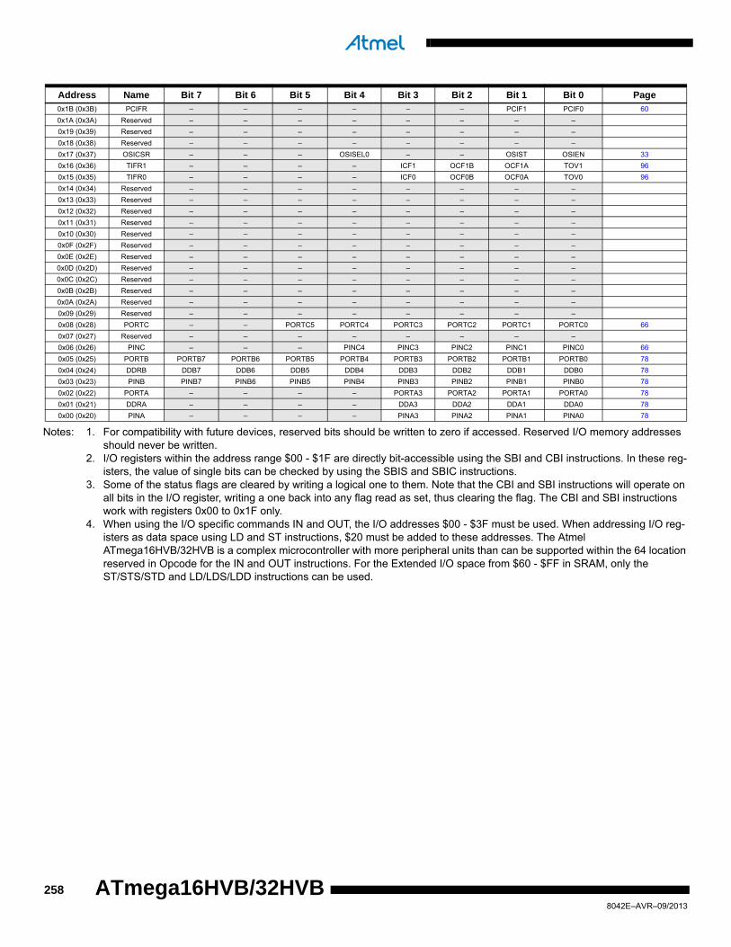
Notes: 1. For compatibility with future devices, reserved bits should be written to zero if accessed. Reserved I/O memory addresses should never be written.
2. I/O registers within the address range $00 - $1F are directly bit-accessible using the SBI and CBI instructions. In these reg-isters, the value of single bits can be checked by using the SBIS and SBIC instructions.
3. Some of the status flags are cleared by writing a logical one to them. Note that the CBI and SBI instructions will operate on all bits in the I/O register, writing a one back into any flag read as set, thus clearing the flag. The CBI and SBI instructions work with registers 0x00 to 0x1F only.
4. When using the I/O specific commands IN and OUT, the I/O addresses $00 - $3F must be used. When addressing I/O reg-isters as data space using LD and ST instructions, $20 must be added to these addresses. The Atmel ATmega16HVB/32HVB is a complex microcontroller with more peripheral units than can be supported within the 64 location reserved in Opcode for the IN and OUT instructions. For the Extended I/O space from $60 - $FF in SRAM, only the ST/STS/STD and LD/LDS/LDD instructions can be used.
0x1B (0x3B) PCIFR – – – – – – PCIF1 PCIF0 60
0x1A (0x3A) Reserved – – – – – – – –
0x19 (0x39) Reserved – – – – – – – –
0x18 (0x38) Reserved – – – – – – – –
0x17 (0x37) OSICSR – – – OSISEL0 – – OSIST OSIEN 33
0x16 (0x36) TIFR1 – – – – ICF1 OCF1B OCF1A TOV1 96
0x15 (0x35) TIFR0 – – – – ICF0 OCF0B OCF0A TOV0 96
0x14 (0x34) Reserved – – – – – – – –
0x13 (0x33) Reserved – – – – – – – –
0x12 (0x32) Reserved – – – – – – – –
0x11 (0x31) Reserved – – – – – – – –
0x10 (0x30) Reserved – – – – – – – –
0x0F (0x2F) Reserved – – – – – – – –
0x0E (0x2E) Reserved – – – – – – – –
0x0D (0x2D) Reserved – – – – – – – –
0x0C (0x2C) Reserved – – – – – – – –
0x0B (0x2B) Reserved – – – – – – – –
0x0A (0x2A) Reserved – – – – – – – –
0x09 (0x29) Reserved – – – – – – – –
0x08 (0x28) PORTC – – PORTC5 PORTC4 PORTC3 PORTC2 PORTC1 PORTC0 66
0x07 (0x27) Reserved – – – – – – – –
0x06 (0x26) PINC – – – PINC4 PINC3 PINC2 PINC1 PINC0 66
0x05 (0x25) PORTB PORTB7 PORTB6 PORTB5 PORTB4 PORTB3 PORTB2 PORTB1 PORTB0 78
0x04 (0x24) DDRB DDB7 DDB6 DDB5 DDB4 DDB3 DDB2 DDB1 DDB0 78
0x03 (0x23) PINB PINB7 PINB6 PINB5 PINB4 PINB3 PINB2 PINB1 PINB0 78
0x02 (0x22) PORTA – – – – PORTA3 PORTA2 PORTA1 PORTA0 78
0x01 (0x21) DDRA – – – – DDA3 DDA2 DDA1 DDA0 78
0x00 (0x20) PINA – – – – PINA3 PINA2 PINA1 PINA0 78
Address Name Bit 7 Bit 6 Bit 5 Bit 4 Bit 3 Bit 2 Bit 1 Bit 0 Page
2588042E–AVR–09/2013
ATmega16HVB/32HVB
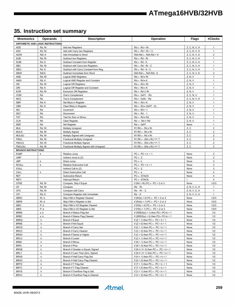
ATmega16HVB/32HVB
35. Instruction set summaryMnemonics Operands Description Operation Flags #Clocks
ARITHMETIC AND LOGIC INSTRUCTIONS
ADD Rd, Rr Add two Registers Rd Rd + Rr Z, C, N, V, H 1
ADC Rd, Rr Add with Carry two Registers Rd Rd + Rr + C Z, C, N, V, H 1
ADIW Rdl, K Add Immediate to Word Rdh:Rdl Rdh:Rdl + K Z, C, N, V, S 2
SUB Rd, Rr Subtract two Registers Rd Rd - Rr Z, C, N, V, H 1
SUBI Rd, K Subtract Constant from Register Rd Rd - K Z, C, N, V, H 1
SBC Rd, Rr Subtract with Carry two Registers Rd Rd - Rr - C Z, C, N, V, H 1
SBCI Rd, K Subtract with Carry Constant from Reg. Rd Rd - K - C Z, C, N, V, H 1
SBIW Rdl,K Subtract Immediate from Word Rdh:Rdl Rdh:Rdl - K Z, C, N, V, S 2
AND Rd, Rr Logical AND Registers Rd Rd Rr Z, N, V 1
ANDI Rd, K Logical AND Register and Constant Rd Rd K Z, N, V 1
OR Rd, Rr Logical OR Registers Rd Rd v Rr Z, N, V 1
ORI Rd, K Logical OR Register and Constant Rd Rd v K Z, N, V 1
EOR Rd, Rr Exclusive OR Registers Rd Rd Rr Z, N, V 1
COM Rd One’s Complement Rd 0xFF Rd Z, C, N, V 1
NEG Rd Two’s Complement Rd 0x00 Rd Z, C, N, V, H 1
SBR Rd, K Set Bit(s) in Register Rd Rd v K Z, N, V 1
CBR Rd, K Clear Bit(s) in Register Rd Rd (0xFF - K) Z, N, V 1
INC Rd Increment Rd Rd + 1 Z, N, V 1
DEC Rd Decrement Rd Rd 1 Z, N, V 1
TST Rd Test for Zero or Minus Rd Rd Rd Z, N, V 1
CLR Rd Clear Register Rd Rd Rd Z, N ,V 1
SER Rd Set Register Rd 0xFF None 1
MUL Rd, Rr Multiply Unsigned R1:R0 Rd x Rr Z, C 2
MULS Rd, Rr Multiply Signed R1:R0 Rd x Rr Z, C 2
MULSU Rd, Rr Multiply Signed with Unsigned R1:R0 Rd x Rr Z, C 2
FMUL Rd, Rr Fractional Multiply Unsigned R1:R0 (Rd x Rr) << 1 Z, C 2
FMULS Rd, Rr Fractional Multiply Signed R1:R0 (Rd x Rr) << 1 Z, C 2
FMULSU Rd, Rr Fractional Multiply Signed with Unsigned R1:R0 (Rd x Rr) << 1 Z, C 2
BRANCH INSTRUCTIONS
RJMP k Relative Jump PC PC + k + 1 None 2
IJMP Indirect Jump to (Z) PC Z None 2
JMP k Direct Jump PC k None 3
RCALL k Relative Subroutine Call PC PC + k + 1 None 3
ICALL Indirect Call to (Z) PC Z None 3
CALL k Direct Subroutine Call PC k None 4
RET Subroutine Return PC STACK None 4
RETI Interrupt Return PC STACK I 4
CPSE Rd, Rr Compare, Skip if Equal if (Rd = Rr) PC PC + 2 or 3 None 1/2/3
CP Rd, Rr Compare Rd Rr Z, N, V, C, H 1
CPC Rd, Rr Compare with Carry Rd Rr C Z, N, V, C, H 1
CPI Rd, K Compare Register with Immediate Rd K Z, N, V, C, H 1
SBRC Rr, b Skip if Bit in Register Cleared if (Rr(b) = 0) PC PC + 2 or 3 None 1/2/3
SBRS Rr, b Skip if Bit in Register is Set if (Rr(b) = 1) PC PC + 2 or 3 None 1/2/3
SBIC P, b Skip if Bit in I/O Register Cleared if (P(b) = 0) PC PC + 2 or 3 None 1/2/3
SBIS P, b Skip if Bit in I/O Register is Set if (P(b) = 1) PC PC + 2 or 3 None 1/2/3
BRBS s, k Branch if Status Flag Set if (SREG(s) = 1) then PCPC+k + 1 None 1/2
BRBC s, k Branch if Status Flag Cleared if (SREG(s) = 0) then PCPC+k + 1 None 1/2
BREQ k Branch if Equal if (Z = 1) then PC PC + k + 1 None 1/2
BRNE k Branch if Not Equal if (Z = 0) then PC PC + k + 1 None 1/2
BRCS k Branch if Carry Set if (C = 1) then PC PC + k + 1 None 1/2
BRCC k Branch if Carry Cleared if (C = 0) then PC PC + k + 1 None 1/2
BRSH k Branch if Same or Higher if (C = 0) then PC PC + k + 1 None 1/2
BRLO k Branch if Lower if (C = 1) then PC PC + k + 1 None 1/2
BRMI k Branch if Minus if (N = 1) then PC PC + k + 1 None 1/2
BRPL k Branch if Plus if (N = 0) then PC PC + k + 1 None 1/2
BRGE k Branch if Greater or Equal, Signed if (N V= 0) then PC PC + k + 1 None 1/2
BRLT k Branch if Less Than Zero, Signed if (N V= 1) then PC PC + k + 1 None 1/2
BRHS k Branch if Half Carry Flag Set if (H = 1) then PC PC + k + 1 None 1/2
BRHC k Branch if Half Carry Flag Cleared if (H = 0) then PC PC + k + 1 None 1/2
BRTS k Branch if T Flag Set if (T = 1) then PC PC + k + 1 None 1/2
BRTC k Branch if T Flag Cleared if (T = 0) then PC PC + k + 1 None 1/2
BRVS k Branch if Overflow Flag is Set if (V = 1) then PC PC + k + 1 None 1/2
BRVC k Branch if Overflow Flag is Cleared if (V = 0) then PC PC + k + 1 None 1/2
2598042E–AVR–09/2013

BRIE k Branch if Interrupt Enabled if ( I = 1) then PC PC + k + 1 None 1/2
BRID k Branch if Interrupt Disabled if ( I = 0) then PC PC + k + 1 None 1/2
BIT AND BIT-TEST INSTRUCTIONS
SBI P, b Set Bit in I/O Register I/O(P,b) 1 None 2
CBI P, b Clear Bit in I/O Register I/O(P,b) 0 None 2
LSL Rd Logical Shift Left Rd(n+1) Rd(n), Rd(0) 0 Z, C, N, V 1
LSR Rd Logical Shift Right Rd(n) Rd(n+1), Rd(7) 0 Z, C, N, V 1
ROL Rd Rotate Left Through Carry Rd(0)C,Rd(n+1) Rd(n),CRd(7) Z, C, N, V 1
ROR Rd Rotate Right Through Carry Rd(7)C,Rd(n) Rd(n+1),CRd(0) Z, C, N, V 1
ASR Rd Arithmetic Shift Right Rd(n) Rd(n+1), n=0..6 Z, C, N, V 1
SWAP Rd Swap Nibbles Rd(3..0)Rd(7..4),Rd(7..4)Rd(3..0) None 1
BSET s Flag Set SREG(s) 1 SREG(s) 1
BCLR s Flag Clear SREG(s) 0 SREG(s) 1
BST Rr, b Bit Store from Register to T T Rr(b) T 1
BLD Rd, b Bit load from T to Register Rd(b) T None 1
SEC Set Carry C 1 C 1
CLC Clear Carry C 0 C 1
SEN Set Negative Flag N 1 N 1
CLN Clear Negative Flag N 0 N 1
SEZ Set Zero Flag Z 1 Z 1
CLZ Clear Zero Flag Z 0 Z 1
SEI Global Interrupt Enable I 1 I 1
CLI Global Interrupt Disable I 0 I 1
SES Set Signed Test Flag S 1 S 1
CLS Clear Signed Test Flag S 0 S 1
SEV Set Twos Complement Overflow. V 1 V 1
CLV Clear Twos Complement Overflow V 0 V 1
SET Set T in SREG T 1 T 1
CLT Clear T in SREG T 0 T 1
SEH Set Half Carry Flag in SREG H 1 H 1
CLH Clear Half Carry Flag in SREG H 0 H 1
DATA TRANSFER INSTRUCTIONS
MOV Rd, Rr Move Between Registers Rd Rr None 1
MOVW Rd, Rr Copy Register Word Rd+1:Rd Rr+1:Rr None 1
LDI Rd, K Load Immediate Rd K None 1
LD Rd, X Load Indirect Rd (X) None 2
LD Rd, X+ Load Indirect and Post-Inc. Rd (X), X X + 1 None 2
LD Rd, - X Load Indirect and Pre-Dec. X X - 1, Rd (X) None 2
LD Rd, Y Load Indirect Rd (Y) None 2
LD Rd, Y+ Load Indirect and Post-Inc. Rd (Y), Y Y + 1 None 2
LD Rd, - Y Load Indirect and Pre-Dec. Y Y - 1, Rd (Y) None 2
LDD Rd, Y+q Load Indirect with Displacement Rd (Y + q) None 2
LD Rd, Z Load Indirect Rd (Z) None 2
LD Rd, Z+ Load Indirect and Post-Inc. Rd (Z), Z Z+1 None 2
LD Rd, -Z Load Indirect and Pre-Dec. Z Z - 1, Rd (Z) None 2
LDD Rd, Z+q Load Indirect with Displacement Rd (Z + q) None 2
LDS Rd, k Load Direct from SRAM Rd (k) None 2
ST X, Rr Store Indirect (X) Rr None 2
ST X+, Rr Store Indirect and Post-Inc. (X) Rr, X X + 1 None 2
ST - X, Rr Store Indirect and Pre-Dec. X X - 1, (X) Rr None 2
ST Y, Rr Store Indirect (Y) Rr None 2
ST Y+, Rr Store Indirect and Post-Inc. (Y) Rr, Y Y + 1 None 2
ST - Y, Rr Store Indirect and Pre-Dec. Y Y - 1, (Y) Rr None 2
STD Y+q, Rr Store Indirect with Displacement (Y + q) Rr None 2
ST Z, Rr Store Indirect (Z) Rr None 2
ST Z+, Rr Store Indirect and Post-Inc. (Z) Rr, Z Z + 1 None 2
ST -Z, Rr Store Indirect and Pre-Dec. Z Z - 1, (Z) Rr None 2
STD Z+q, Rr Store Indirect with Displacement (Z + q) Rr None 2
STS k, Rr Store Direct to SRAM (k) Rr None 2
LPM Load Program Memory R0 (Z) None 3
LPM Rd, Z Load Program Memory Rd (Z) None 3
LPM Rd, Z+ Load Program Memory and Post-Inc Rd (Z), Z Z+1 None 3
SPM Store Program Memory (Z) R1:R0 None -
IN Rd, P In Port Rd P None 1
35. Instruction set summary (Continued)Mnemonics Operands Description Operation Flags #Clocks
2608042E–AVR–09/2013
ATmega16HVB/32HVB

ATmega16HVB/32HVB
OUT P, Rr Out Port P Rr None 1
PUSH Rr Push Register on Stack STACK Rr None 2
POP Rd Pop Register from Stack Rd STACK None 2
MCU CONTROL INSTRUCTIONS
NOP No Operation None 1
SLEEP Sleep (see specific descr. for Sleep function) None 1
WDR Watchdog Reset (see specific descr. for WDR/timer) None 1
BREAK Break For On-chip Debug Only None N/A
35. Instruction set summary (Continued)Mnemonics Operands Description Operation Flags #Clocks
2618042E–AVR–09/2013
36. Ordering information
36.1 The Atmel ATmega16HVB
Speed (MHz) Power supply Ordering code Package Operation range
1MHz - 8MHz 4V - 18V ATMEGA16HVB-8X3 44X1 -40C to 85C
Package type
44X1 44-lead, 4.4mm body width, plastic thin shrink small outline package (TSSOP)
2628042E–AVR–09/2013
ATmega16HVB/32HVB

ATmega16HVB/32HVB
36.2 The Atmel ATmega32HVB
Speed (MHz) Power supply Ordering code Package Operation range
1MHz - 8MHz 4V - 18V ATMEGA32HVB-8X3 44X1 -40C to 85C
Package type
44X1 44-lead, 4.4mm body width, plastic thin shrink small outline package (TSSOP)
2638042E–AVR–09/2013

37. Packaging information
37.1 44X1
TITLE DRAWING NO.
R
REV.
Note: These drawings are for general information only. Refer to JEDEC Drawing MO-153BE.
2325 Orchard Parkway San Jose, CA 95131
5/16/07
44X1, 44-lead, 4.4 mm Body Width, Plastic Thin ShrinkSmall Outline Package (TSSOP) 44X1 A
COMMON DIMENSIONS(Unit of Measure = mm)
SYMBOL MIN NOM MAX NOTE
A – – 1.20
A1 0.05 –
b 0.17 – 0.27
C 0.09 – 0.20
D 10.90 11.00 11.10
E1 4.30 4.40 4.50
E 6.20 6.40 6.60
e 0.50 TYP
L 0.50 0.60 0.70
Ø 0o – 8o
Side View
Top View
End View
Ø
1
44
23
L
C
E1 E
D
e
b
A
A1
0.15
TITLE DRAWING NO.
R
REV.
Note: These drawings are for general information only. Refer to JEDEC Drawing MO-153BE.
2325 Orchard Parkway San Jose, CA 95131
5/16/07
44X1, 44-lead, 4.4mm Body Width, Plastic Thin ShrinkSmall Outline Package (TSSOP) 44X1 A
COMMON DIMENSIONS(Unit of Measure = mm)
SYMBOL MIN NOM MAX NOTE
A – – 1.20
A1 0.05 – 0.15
b 0.17 – 0.27
C 0.09 – 0.20
D 10.90 11.00 11.10
E1 4.30 4.40 4.50
E 6.20 6.40 6.60
e 0.50 TYP
L 0.50 0.60 0.70
Ø 0o – 8o
Side View
Top View
End View
Ø
1
44
23
L
C
E1 E
D
e
b
A
A1
2648042E–AVR–09/2013
ATmega16HVB/32HVB
ATmega16HVB/32HVB
38. Errata
38.1 The Atmel ATmega16HVB
38.1.1 Rev. E
TWI bus can get stuck if TWI STOP condition bit is set in slave mode
If the TWSTO bit in TWCR is set while the TWI starts to receive data in slave mode, it can resultin pulling the SCL pin low and then the TWI bus will get stuck. To release the SCL pin and getout of this situation the TWI module needs to be disabled and then re-enabled.
Problem fix/workaround
While in slave mode the TWSTO bit should be written only to recover from an error condition andthen cleared before a data transfer starts.
38.1.2 Rev. D
Not sampled.
38.1.3 Rev. C
TWI bus can get stuck if TWI STOP condition bit is set in slave mode
If the TWSTO bit in TWCR is set while the TWI starts to receive data in slave mode, it can resultin pulling the SCL pin low and then the TWI bus will get stuck. To release the SCL pin and getout of this situation the TWI module needs to be disabled and then re-enabled.
Problem fix/workaround
While in slave mode the TWSTO bit should be written only to recover from an error condition andthen cleared before a data transfer starts.
38.1.4 Rev. B
Stack pointer initial value
The stack pointer in ATmega16HVB is incorrectly initialized to 0x08ff instead of 0x04ff.
Problem fix/workaround
Initialize the stack pointer in software before the stack is used. Most C-compilers does initial-ize the stack pointer without manual intervention.
Assembly Code Example:
ldi r16,high(RAMEND); Main program start out SPH,r16 ; Set Stack Pointer to top of RAM ldir16,low(RAMEND) out SPL,r16 C Code Example (if required): SP = RAMEND;
TWI bus can get stuck if TWI STOP condition bit is set in slave mode
If the TWSTO bit in TWCR is set while the TWI starts to receive data in slave mode, it can resultin pulling the SCL pin low and then the TWI bus will get stuck. To release the SCL pin and getout of this situation the TWI module needs to be disabled and then re-enabled.
Problem fix/workaround
While in slave mode the TWSTO bit should be written only to recover from an error condition andthen cleared before a data transfer starts.
38.1.5 Rev. A
Not sampled.
2658042E–AVR–09/2013
38.2 The Atmel ATmega32HVB
38.2.1 Rev. E
TWI bus can get stuck if TWI STOP condition bit is set in slave mode
If the TWSTO bit in TWCR is set while the TWI starts to receive data in slave mode, it can resultin pulling the SCL pin low and then the TWI bus will get stuck. To release the SCL pin and getout of this situation the TWI module needs to be disabled and then re-enabled.
Problem fix/workaround
While in slave mode the TWSTO bit should be written only to recover from an error condition andthen cleared before a data transfer starts.
38.2.2 Rev. D
Not sampled.
38.2.3 Rev. C
TWI bus can get stuck if TWI STOP condition bit is set in slave mode
If the TWSTO bit in TWCR is set while the TWI starts to receive data in slave mode, it can resultin pulling the SCL pin low and then the TWI bus will get stuck. To release the SCL pin and getout of this situation the TWI module needs to be disabled and then re-enabled.
Problem fix/workaround
While in slave mode the TWSTO bit should be written only to recover from an error condition andthen cleared before a data transfer starts.
38.2.4 Rev. B
TWI bus can get stuck if TWI STOP condition bit is set in slave mode
If the TWSTO bit in TWCR is set while the TWI starts to receive data in slave mode, it can resultin pulling the SCL pin low and then the TWI bus will get stuck. To release the SCL pin and getout of this situation the TWI module needs to be disabled and then re-enabled.
Problem fix/workaround
While in slave mode the TWSTO bit should be written only to recover from an error condition andthen cleared before a data transfer starts.
38.2.5 Rev. A
Not sampled.
2668042E–AVR–09/2013
ATmega16HVB/32HVB

ATmega16HVB/32HVB
39. Revision history
Please note that the referring page numbers in this section are referring to this document. Thereferring revision in this section are referring to the document revision.
39.1 Rev. 8042E-09/2013
39.2 Rev. 8042D-10/2011
1. Updated ”Errata” on page 265:
ATmega16HVB: Added errata sections for “Rev. C” , “Rev. D” and “Rev. E” .
ATmega32HVB: Added errata sections for “Rev. B” , “Rev. C” , “Rev. D” and “Rev. E” .
1. Operating voltage has been changed from 4V - 25V to 4V - 18V
2. The methods for determing the actual clock period of the ULP Oscillator i Section 9.2.3 on page 27 have been changed
3. In ”Bit 1:0 – CLKPS[1:0]: Clock Prescaler select Bit[1:0]” on page 33 new text has been inserted in and the text “If CKDIBV8 is programmed” has been corrected to “If CKDIV8 is programmed”
4. Note 2 in ”Bit 0 – OSIEN: Oscillator sampling interface enable” on page 34 has been deleted
5. Figure 11-1 on page 43 has been corrected
6. New Note 2 has been added below Table 11-2 on page 51
7. The last sentence in Section 21.5 on page 123 has been corrected
8. The text in Section 25.3.1 on page 146 below Figure 25-2 has been corrected several places
9. VCC in Figure 28-1 on page 186 has been corrected
10. Bit no 4 in Table 30-3 on page 205 has been corrected
11. Note 1 below Table 30-3 on page 205 has been corrected
12. The text in point 4 and 5 in Section 30.6.1 on page 208 has been corrected
13. The VFET value in Figure 30-3 on page 212 has been corrected
14. The table in Section 32.1 on page 225 hase been updated with several new values
15. ILOAD in Table 32-2 on page 226 has been added
16. Note 1 below Table 32-2 on page 226 has been added
17. The maximum value for VBOT in Table 32-3 on page 227 has been added
18. In Table 32-4 on page 227 the maximum value for VRSCL has been corrected and the maximum value for VREG pin has been added
19. In Table 32-7 on page 229 the typical and maximum values for INL has been corrected
20. In Table 32-8 on page 229 the typical value for frequency prediction error (slow RC oscillator) has been corrected
21. In Table 32-10 on page 230 the text below “Parameter” has been corrected
22. In Table 32-12 on page 231 Note 5 has been added
2678042E–AVR–09/2013

39.3 Rev. 8042C-06/2011
23. In Table 32-18 on page 236 the maximum value for tWLRH_CE has been corrected
24. The former figure “Active supply current vs. VVFET, WDT, VREF, CBP, OC/OD and CC-ADC enabled” on page 238 has been removed
25. In Table 33-1 on page 243 the text “CC-OD” has benn changed to “OC-OD” and below “Typical current consumption” the value “55µA” has been changed to “85µA”
26. New text is added below the two notes for Table 33-1 on page 243
27. New Figure 33-11 on page 245 “Power-save supply current vs. VVFET, WDT, VREF, CBP, OC/OD, and CC-ADC enabled” is added
28. The plot in Figure 33-13 on page 246 has been updated
29. The plot in Figure 33-14 on page 246 has been updated
30. New Figure 33-15 on page 247 has been added
31. New Figure 33-21 on page 250 has been added
32. Heading in Figure 33-27 on page 253 has been corrected
33. The power supply voltage in the table in Section 36.1 on page 262 has been corrected
34. The power supply voltage in the table in Section 36.2 on page 263 has been corrected
35. The Section 38. on page 265 has been corrected by adding an errata for “all revisions”
36. The text “...clock period of the Slow RC Oscillator...” in point 2 in Section 9.2.3 on page 27 has been corrected to “...clock period of the ULP RC Oscillator...”
37. Note 1 below Table 19-1 on page 112 has been corrected
38. Note 1 below Table 19-2 on page 112 has been corrected
39. Figure 31-1 on page 220 has been updated
40. Figure 31-2 on page 221 has been updated
41. Figure 31-3 on page 222 has been updated
42. Table 31-1 on page 223 has been updated according to the changes in Figure 31-1 on page 220, Figure 31-2 on page 221, and Figure 31-3 on page 222
1. The columns “Minimum” and “Maximum” in Table 24-5 on page 142 are deleted
2. A new row (“Device lot ID and position”) in Table 29-3 on page 196 is added
3. A new note (“Note 16”) in Table 29-3 on page 196 is added
4. In ”Absolute maximum ratings*” on page 225 the following values have been changed: “Voltage on OC and OD with respect to ground”, “Voltage on PC5, BATT, PVT, VFET, PV4, PV3, and PV2 with respect to ground”, and “Maximum operating voltage on VFET”
5. In Table 32-1 on page 225 the values for “Typical” and “Maximum” in the row “VFET = 16V, WDT, CC-ADC, OC, OD, and battery protection enabled, DUVR mode disabled” are added
6. “Frequency drift” for “Slow RC oscillator” in Table 32-8 on page 229 is deleted
7. A new note (“Note 4”) in Table 32-8 on page 229 is added
8. Table 32-10 on page 230 is updated and corrected
2688042E–AVR–09/2013
ATmega16HVB/32HVB
ATmega16HVB/32HVB
39.4 Rev. 8042B-06/2010
39.5 Rev. 8042A-08/2009
9. The text “CEQ = 4.7nF, VFET = 16V” is added to “Condition” for tf,OC and tf,OD in Table 32-2 on page 226
10. New Figure 33-1 on page 238 is added
11. Corrected formula in Table 32-15 on page 232
12. Corrected and added some short-cuts in addition to general update and some minor corrections in text
1. Removed direction arrow in Figure 17-1 on page 82.
2. Updated ”Configuring PA1 and PA0 for V-ADC operation” on page 117.
3. Updated ”Operating circuit” on page 220, with correct naming convention for thermistors RT32 and RT33.
1. Initial revision
2698042E–AVR–09/2013

2708042E–AVR–09/2013
ATmega16HVB/32HVB
ATmega16HVB/32HVB
Table of Contents
Features ..................................................................................................... 1
1 Pin configurations .................................................................................... 2
1.1TSSOP ......................................................................................................................2
1.2Pin descriptions .........................................................................................................3
2 Overview ................................................................................................... 5
2.1Comparison between the Atmel ATmega16HVB and the Atmel ATmega32HVB .....7
3 Disclaimer ................................................................................................. 8
4 Resources ................................................................................................. 8
5 About code examples .............................................................................. 8
6 Data retention ........................................................................................... 8
7 AVR CPU core .......................................................................................... 9
7.1Overview ....................................................................................................................9
7.2ALU – Arithmetic Logic Unit .....................................................................................10
7.3Status Register ........................................................................................................10
7.4General purpose Register File .................................................................................12
7.5Stack Pointer ...........................................................................................................13
7.6Instruction execution timing .....................................................................................14
7.7Reset and interrupt handling ...................................................................................14
8 AVR memories ........................................................................................ 17
8.1Overview ..................................................................................................................17
8.2In-system reprogrammable flash program memory .................................................17
8.3SRAM data memory ................................................................................................17
8.4EEPROM data memory ...........................................................................................19
8.5I/O memory ..............................................................................................................19
8.6Register description .................................................................................................20
9 System clock and clock options ........................................................... 25
9.1Clock systems and their distribution ........................................................................25
9.2Clock sources ..........................................................................................................26
9.3Clock startup sequence ...........................................................................................28
9.4Clock output .............................................................................................................28
9.5System clock prescaler ............................................................................................28
18042E–AVR–09/2013

9.6VADC clock prescaler ..............................................................................................29
9.7OSI – Oscillator sampling interface .........................................................................29
9.8Register description .................................................................................................32
10 Power management and sleep modes ................................................. 35
10.1Sleep modes ..........................................................................................................35
10.2Idle mode ...............................................................................................................37
10.3ADC noise reduction ..............................................................................................37
10.4Power-save mode ..................................................................................................37
10.5Power-off mode .....................................................................................................38
10.6Power Reduction Register .....................................................................................38
10.7Minimizing power consumption .............................................................................38
10.8Register description ...............................................................................................39
11 System control and reset ...................................................................... 42
11.1Resetting the AVR .................................................................................................42
11.2Reset sources ........................................................................................................42
11.3Reset and the voltage reference ...........................................................................45
11.4Watchdog timer .....................................................................................................46
11.5Register description ...............................................................................................49
12 Interrupts ................................................................................................ 52
12.1Overview ................................................................................................................52
12.2Interrupt vectors in Atmel ATmega16HVB/32HVB ................................................52
12.3Moving interrupts between application and boot space .........................................56
12.4Register description ...............................................................................................56
13 External interrupts ................................................................................. 58
13.1Overview ................................................................................................................58
13.2Register description ...............................................................................................58
14 High voltage I/O ports ............................................................................ 62
14.1Overview ................................................................................................................62
14.2High voltage ports as general digital I/O ................................................................63
14.3Overview ................................................................................................................64
14.4Alternate port functions ..........................................................................................64
14.5Register description ...............................................................................................66
15 Low voltage I/O-Ports ............................................................................ 67
15.1Overview ................................................................................................................67
28042E–AVR–09/2013
ATmega16HVB/32HVB
ATmega16HVB/32HVB
15.2Low voltage ports as general digital I/O ................................................................68
15.3Alternate port functions ..........................................................................................72
15.4Register description ...............................................................................................78
16 Timer/Counter0 and Timer/Counter1 prescalers ................................. 79
16.1Overview ................................................................................................................79
16.2External clock source ............................................................................................80
16.3Register description ...............................................................................................81
17 Timer/Counter (T/C0,T/C1) ..................................................................... 82
17.1Features ................................................................................................................82
17.2Overview ................................................................................................................82
17.3Timer/Counter clock sources .................................................................................83
17.4Counter unit ...........................................................................................................83
17.5Modes of operation ................................................................................................84
17.6Input capture unit ...................................................................................................86
17.7Output compare unit ..............................................................................................88
17.8Timer/counter timing diagrams ..............................................................................89
17.9Accessing registers in 16-bit mode ........................................................................90
17.10Register description .............................................................................................94
18 SPI – Serial Peripheral Interface ........................................................... 98
18.1Features ................................................................................................................98
18.2Overview ................................................................................................................98
18.3SS pin functionality ..............................................................................................103
18.4Data modes .........................................................................................................103
18.5Register description .............................................................................................105
19 Coulomb counter – Dedicated fuel gauging Sigma-Delta ADC ...... 108
19.1Features ..............................................................................................................108
19.2Overview ..............................................................................................................108
19.3Normal operation .................................................................................................109
19.4Regular current detection operation ....................................................................110
19.5Offset canceling by polarity switching ..................................................................110
19.6Configuration and usage .....................................................................................111
19.7Register description .............................................................................................111
20 Voltage ADC – 7-channel general purpose 12-bit Sigma-Delta ADC 116
20.1Features ..............................................................................................................116
38042E–AVR–09/2013

20.2Overview ..............................................................................................................116
20.3Operation .............................................................................................................116
20.4Register description .............................................................................................119
21 Voltage reference and temperature sensor ....................................... 122
21.1Features ..............................................................................................................122
21.2Overview ..............................................................................................................122
21.3Operation .............................................................................................................122
21.4Bandgap calibration .............................................................................................123
21.5Bandgap buffer settling time ................................................................................123
21.6Register description .............................................................................................124
22 Charger detect ...................................................................................... 126
22.1Features ..............................................................................................................126
22.2Overview ..............................................................................................................126
22.3Operation .............................................................................................................127
22.4Register description .............................................................................................128
23 Voltage regulator .................................................................................. 129
23.1Features ..............................................................................................................129
23.2Overview ..............................................................................................................129
23.3Regulator start-up ................................................................................................130
23.4Battery pack short detection ................................................................................130
23.5Black-out detection ..............................................................................................130
23.6Register description .............................................................................................131
24 Battery protection ................................................................................ 132
24.1Features ..............................................................................................................132
24.2Overview ..............................................................................................................132
24.3Operation .............................................................................................................133
24.4External protection input ......................................................................................134
24.5Optimizing usage for low power consumption .....................................................136
24.6Battery protection CPU interface .........................................................................137
24.7Register description .............................................................................................137
25 FET driver ............................................................................................. 145
25.1Features ..............................................................................................................145
25.2Overview ..............................................................................................................145
25.3Operation and usage ...........................................................................................146
48042E–AVR–09/2013
ATmega16HVB/32HVB

ATmega16HVB/32HVB
25.4Register description .............................................................................................149
26 Cell balancing ....................................................................................... 151
26.1Overview ..............................................................................................................151
26.2Register description .............................................................................................152
27 2-wire serial interface .......................................................................... 153
27.1Features ..............................................................................................................153
27.2Two-wire serial interface bus definition ...............................................................153
27.3Data transfer and frame format ...........................................................................154
27.4Multi-master bus systems, arbitration and synchronization .................................157
27.5Overview of the TWI module ...............................................................................159
27.6Using the TWI ......................................................................................................162
27.7Transmission modes ...........................................................................................165
27.8Multi-master systems and arbitration ...................................................................178
27.9Bus connect/disconnect for two-wire serial interface ...........................................179
27.10Register description ...........................................................................................181
28 debugWIRE on-chip debug system .................................................... 186
28.1Features ..............................................................................................................186
28.2Overview ..............................................................................................................186
28.3Physical interface ................................................................................................186
28.4Software break points ..........................................................................................187
28.5Limitations of debugWIRE ...................................................................................187
28.6Register description .............................................................................................187
29 Boot loader support – Read-while-write self-programming ............. 188
29.1Features ..............................................................................................................188
29.2Overview ..............................................................................................................188
29.3Application and boot loader flash sections ..........................................................188
29.4Read-while-write and no read-while-write flash sections .....................................189
29.5Boot loader lock bits ............................................................................................191
29.6Entering the boot loader program ........................................................................192
29.7Addressing the flash during self-programming ....................................................192
29.8Self-programming the flash .................................................................................193
29.9Register description .............................................................................................202
30 Memory programming ......................................................................... 204
30.1Program and data memory lock bits ....................................................................204
58042E–AVR–09/2013
30.2Fuse bits ..............................................................................................................205
30.3Signature bytes ....................................................................................................206
30.4Calibration bytes ..................................................................................................207
30.5Page size .............................................................................................................207
30.6Serial programming .............................................................................................207
30.7Parallel programming ..........................................................................................211
31 Operating circuit .................................................................................. 220
32 Electrical characteristics ..................................................................... 225
32.1Absolute maximum ratings* .................................................................................225
32.2Supply current characteristics .............................................................................225
32.3NFET driver characteristics .................................................................................226
32.4Reset characteristics ...........................................................................................227
32.5Voltage regulator characteristics .........................................................................227
32.6Voltage reference and temperature sensor characteristics .................................227
32.7ADC characteristics .............................................................................................228
32.8Clock characteristics ............................................................................................229
32.9Cell balancing characteristic ................................................................................230
32.10Battery protection characteristics ......................................................................230
32.11External interrupt characteristics .......................................................................230
32.12General I/O lines characteristics ........................................................................231
32.132-wire serial interface characteristics ................................................................232
32.14SPI timing characteristics ..................................................................................233
32.15Serial programming characteristics ...................................................................234
32.16Parallel programming characteristics ................................................................235
33 Typical characteristics ........................................................................ 238
33.1Supply current characteristics .............................................................................238
33.2NFET driver characteristics .................................................................................245
33.3Battery protection characteristics ........................................................................248
33.4Clock characteristics ............................................................................................248
33.5Voltage reference characteristics ........................................................................251
33.6Voltage regulator characteristics .........................................................................252
33.7BOD threshold characteristics .............................................................................254
34 Register summary ................................................................................ 255
35 Instruction set summary ..................................................................... 259
68042E–AVR–09/2013
ATmega16HVB/32HVB
ATmega16HVB/32HVB
36 Ordering information ........................................................................... 262
36.1The Atmel ATmega16HVB ..................................................................................262
36.2The Atmel ATmega32HVB ..................................................................................263
37 Packaging information ........................................................................ 264
37.144X1 ....................................................................................................................264
38 Errata ..................................................................................................... 265
38.1The Atmel ATmega16HVB ..................................................................................265
38.2The Atmel ATmega32HVB ..................................................................................266
39 Revision history ................................................................................... 267
39.1Rev. 8042E-09/2013 ............................................................................................267
39.2Rev. 8042D-10/2011 ...........................................................................................267
39.3Rev. 8042C-06/2011 ...........................................................................................268
39.4Rev. 8042B-06/2010 ............................................................................................269
39.5Rev. 8042A-08/2009 ............................................................................................269
Table of Contents...................................................................................... 1
78042E–AVR–09/2013

Atmel Corporation
1600 Technology Drive
San Jose, CA 95110
USA
Tel: (+1) (408) 441-0311
Fax: (+1) (408) 487-2600
www.atmel.com
Atmel Asia Limited
Unit 01-5 & 16, 19F
BEA Tower, Millennium City 5
418 Kwun Tong Roa
Kwun Tong, Kowloon
HONG KONG
Tel: (+852) 2245-6100
Fax: (+852) 2722-1369
Atmel Munich GmbH
Business Campus
Parkring 4
D-85748 Garching b. Munich
GERMANY
Tel: (+49) 89-31970-0
Fax: (+49) 89-3194621
Atmel Japan G.K.
16F Shin-Osaki Kangyo Bldg
1-6-4 Osaki, Shinagawa-ku
Tokyo 141-0032
JAPAN
Tel: (+81) (3) 6417-0300
Fax: (+81) (3) 6417-0370
© 2013 Atmel Corporation. All rights reserved. / Rev.: 8042E–AVR–09/2013
Disclaimer: The information in this document is provided in connection with Atmel products. No license, express or implied, by estoppel or otherwise, to any intellectual property right is granted by this document or in connection with the sale of Atmel products. EXCEPT AS SET FORTH IN THE ATMEL TERMS AND CONDITIONS OF SALES LOCATED ON THE ATMEL WEBSITE, ATMEL ASSUMES NO LIABILITY WHATSOEVER AND DISCLAIMS ANY EXPRESS, IMPLIED OR STATUTORY WARRANTY RELATING TO ITS PRODUCTS INCLUDING, BUT NOT LIMITED TO, THE IMPLIED WARRANTY OF MERCHANTABILITY, FITNESS FOR A PARTICULAR PURPOSE, OR NON-INFRINGEMENT. IN NO EVENT SHALL ATMEL BE LIABLE FOR ANY DIRECT, INDIRECT, CONSEQUENTIAL, PUNITIVE, SPECIAL OR INCIDENTAL DAMAGES (INCLUDING, WITHOUT LIMITATION, DAMAGES FOR LOSS AND PROFITS, BUSINESS INTERRUPTION, OR LOSS OF INFORMATION) ARISING OUT OF THE USE OR INABILITY TO USE THIS DOCUMENT, EVEN IF ATMEL HAS BEEN ADVISED OF THE POSSIBILITY OF SUCH DAMAGES. Atmel makes no representations or warranties with respect to the accuracy or completeness of the contents of this document and reserves the right to make changes to specifications and products descriptions at any time without notice. Atmel does not make any commitment to update the information contained herein. Unless specifically provided otherwise, Atmel products are not suitable for, and shall not be used in,
Atmel®, Atmel logo and combinations thereof, Enabling Unlimited Possibilities®, AVR® and others are registered trademarks or trademarks of Atmel Corporation or its subsidiaries. Other terms and product names may be trademarks of others.
8042E–AVR–09/2013
automotive applications. Atmel products are not intended, authorized, or warranted for use as components in applications intended to support or sustain life.