Embed Size (px)
Citation preview

7647C–AVR–07/08
8-bit Microcontroller with 16K/32K/64K Bytes In-SystemProgrammable Flash
ATmega16M1ATmega32M1ATmega64M1ATmega32C1ATmega64C1
Automotive
Preliminary
Features• High Performance, Low Power AVR ® 8-bit Microcontroller• Advanced RISC Architecture
– 131 Powerful Instructions - Most Single Clock Cycle Execution– 32 x 8 General Purpose Working Registers– Fully Static Operation– Up to 1 MIPS throughput per MHz– On-chip 2-cycle Multiplier
• Data and Non-Volatile Program Memory– 16K/32K/64K Bytes Flash of In-System Programmable Program Memory
• Endurance: 10,000 Write/Erase Cycles– Optional Boot Code Section with Independent Lock Bits– In-System Programming by On-chip Boot Program
• True Read-While-Write Operation– 512/1024/2048 Bytes of In-System Programmable EEPROM
• Endurance: 50,000 Write/Erase Cycles• Programming Lock for Flash Program and EEPROM Data Security• 1024/2048/4096 Bytes Internal SRAM • On Chip Debug Interface (debugWIRE)• CAN 2.0A/B with 6 Message Objects - ISO 16845 Certified (1)
• LIN 2.1 and 1.3 Controller or 8-Bit UART• One 12-bit High Speed PSC (Power Stage Controller) (only ATmega16/32/64M1)
• Non Overlapping Inverted PWM Output Pins With Flexible Dead-Time • Variable PWM duty Cycle and Frequency• Synchronous Update of all PWM Registers• Auto Stop Function for Emergency Event
• Peripheral Features– One 8-bit General purpose Timer/Counter with Separate Prescaler, Compare Mode
and Capture Mode– One 16-bit General purpose Timer/Counter with Separate Prescaler, Compare
Mode and Capture Mode– One Master/Slave SPI Serial Interface– 10-bit ADC
• Up To 11 Single Ended Channels and 3 Fully Differential ADC Channel Pairs• Programmable Gain (5x, 10x, 20x, 40x) on Differential Channels• Internal Reference Voltage• Direct Power Supply Voltage Measurement
– 10-bit DAC for Variable Voltage Reference (Comparators, ADC)– Four Analog Comparators with Variable Threshold Detection– 100µA ±3% Current Source (LIN Node Identification)– Interrupt and Wake-up on Pin Change– Programmable Watchdog Timer with Separate On-Chip Oscillator– On-chipTemperature Sensor
• Special Microcontroller Features– Low Power Idle, Noise Reduction, and Power Down Modes– Power On Reset and Programmable Brown Out Detection– In-System Programmable via SPI Port– High Precision Crystal Oscillator for CAN Operations (16 MHz)
1. See certification on Atmel web site. And note on Section 16.4.3 on page 175.

– Internal Calibrated RC Oscillator ( 8 MHz)– On-chip PLL for fast PWM ( 32 MHz, 64 MHz) and CPU (16 MHz)
• Operating Voltage: 2.7V - 5.5V • Extended Operating Temperature:
– -40°C to +125°C• Core Speed Grade:
– 0 - 8MHz @ 2.7 - 4.5V– 0 - 16MHz @ 4.5 - 5.5V
ATmega32/64/M1/C1 Product Line-up
Part number ATmega32C1 ATmega64C1 ATmega16M1 ATmega32M1 ATmega64M1
Flash Size 32 Kbyte 64 Kbyte 16 Kbyte 32 Kbyte 64 Kbyte
RAM Size 2048 bytes 4096 bytes 1024 bytes 2048 bytes 4096 bytes
EEPROM Size 1024 bytes 2048 bytes 512 bytes 1024 bytes 2048 bytes
8-bit Timer Yes
16-bit Timer Yes
PSC No Yes
PWM Outputs 4 4 10 10 10
Fault Inputs (PSC) 0 0 3 3 3
PLL 32/64 MHz
10-bit ADC Channels 11 single3 Differential
10-bit DAC Yes
Analog Comparators 4
Current Source Yes
CAN Yes
LIN/UART Yes
On-Chip Temp. Sensor Yes
SPI Interface Yes
27647C–AVR–07/08
ATmega16/32/64/M1/C1

ATmega16/32/64/M1/C1
1. Pin Configurations
Figure 1-1. ATmega16/32/64M1 TQFP32/QFN32 (7*7 mm) Package.
Note: On the engineering samples (Parts marked AT90PWM324), the ACMPN3 alternate function is not located on PC4. It is located on PE2.
12345678
2423222120191817
(PCINT18/PSCIN2/OC1A/MISO_A) PD2(PCINT19/TXD/TXLIN/OC0A/SS/MOSI_A) PD3
(PCINT9/PSCIN1/OC1B/SS_A) PC1VCC
GND (PCINT10/T0/TXCAN) PC2
(PCINT11/T1/RXCAN/ICP1B) PC3(PCINT0/MISO/PSCOUT2A) PB0
PB4 (AMP0+/PCINT4) PB3 (AMP0-/PCINT3)PC6 (ADC10/ACMP1/PCINT14)AREF(ISRC)AGNDAVCCPC5 (ADC9/ACMP3/AMP1+/PCINT13)PC4 (ADC8/ACMPN3/AMP1-/PCINT12)
32 31 30 29 28 27 26 25
9 10 11 12 13 14 15 16
(PCI
NT1
/MO
SI/P
SCO
UT2
B) P
B1(P
CIN
T25/
OC0
B/XT
AL1
) PE1
(PCI
NT2
6/A
DC0
/XTA
L2) P
E2(P
CIN
T20/
AD
C1/R
XD/R
XLIN
/ICP
1A/S
CK_A
) PD
4(A
DC2
/ACM
P2/P
CIN
T21)
PD
5 (A
DC3
/ACM
PN2/
INT0
/PCI
NT2
2) P
D6
(ACM
P0/P
CIN
T23)
PD
7
(A
DC5
/IN
T1/A
CMPN
0/PC
INT2
) PB2
PD1(
PCIN
T17/
PSCI
N0/
CLKO
)PE
0 (P
CIN
T24/
RESE
T/O
CD)
PC0(
PCIN
T8/I
NT3
/PSC
OU
T1A
) PD
0 (P
CIN
T16/
PSCO
UT0
A)
PB7
(AD
C4/P
SCO
UT0
B/SC
K/PC
INT7
)PB
6 (A
DC7
/PSC
OU
T1B/
PCIN
T6)
PB5
(AD
C6/I
NT2
/ACM
PN1/
AM
P2-/
PCIN
T5)
PC7
(D2A
/AM
P2+
/PCI
NT1
5)
ATmega32/64M1 TQFP32/QFN32
37647C–AVR–07/08

Figure 1-2. ATmega32/64C1 TQFP32/QFN32 (7*7 mm) Package
Note: On the first engineering samples (Parts marked AT90PWM324), the ACMPN3 alternate function is not located on PC4. It is located on PE2.
12345678
2423222120191817
(PCINT18/OC1A/MISO_A) PD2(PCINT19/TXD/TXLIN/OC0A/SS/MOSI_A) PD3
(PCINT9/OC1B/SS_A) PC1VCCGND
(PCINT10/T0/TXCAN) PC2(PCINT11/T1/RXCAN/ICP1B) PC3
(PCINT0/MISO) PB0
PB4 (AMP0+/PCINT4) PB3 (AMP0-/PCINT3)PC6 (ADC10/ACMP1/PCINT14)AREF(ISRC)AGNDAVCCPC5 (ADC9/ACMP3/AMP1+/PCINT13)PC4 (ADC8/ACMPN3/AMP1-/PCINT12)
32 31 30 29 28 27 26 25
9 10 11 12 13 14 15 16
(PC
INT1
/MO
SI)
PB
1(P
CIN
T25/
OC
0B/X
TAL1
) PE
1(P
CIN
T26/
AD
C0/
XTA
L2) P
E2
(PC
INT2
0/A
DC
1/R
XD
/RX
LIN
/ICP
1A/S
CK
_A) P
D4
(AD
C2/
AC
MP
2/P
CIN
T21)
PD
5 (A
DC
3/A
CM
PN
2/IN
T0/P
CIN
T22)
PD
6 (A
CM
P0/
PC
INT2
3) P
D7
(A
DC
5/IN
T1/A
CM
PN
0/P
CIN
T2) P
B2
PD
1(P
CIN
T17/
CLK
O)
PE
0 (P
CIN
T24/
RE
SE
T/O
CD
)P
C0(
PC
INT8
/INT3
) P
D0
(PC
INT1
6)P
B7
(AD
C4/
SC
K/P
CIN
T7)
PB
6 (A
DC
7PC
INT6
)P
B5
(AD
C6/
INT2
/AC
MP
N1/
AM
P2-
/PC
INT5
)P
C7
(D2A
/AM
P2+
/PC
INT1
5)
ATmega32/64C1 TQFP32/QFN32
47647C–AVR–07/08
ATmega16/32/64/M1/C1

ATmega16/32/64/M1/C1
1.1 Pin Descriptions
: Table 1-1. Pin out description
QFN32 Pin Number Mnemonic Type Name, Function & Alternate Function
5 GND Power Ground: 0V reference
20 AGND Power Analog Ground: 0V reference for analog part
4 VCC Power Power Supply
19 AVCC PowerAnalog Power Supply: This is the power supply voltage for analog partFor a normal use this pin must be connected.
21 AREF Power
Analog Reference : reference for analog converter . This is the reference voltage of the A/D converter. As output, can be used by external analogISRC (Current Source Output)
8 PB0 I/OMISO (SPI Master In Slave Out)PSCOUT2A(1) (PSC Module 2 Output A)PCINT0 (Pin Change Interrupt 0)
9 PB1 I/OMOSI (SPI Master Out Slave In)PSCOUT2B(1) (PSC Module 2 Output B)PCINT1 (Pin Change Interrupt 1)
16 PB2 I/O
ADC5 (Analog Input Channel 5 )INT1 (External Interrupt 1 Input)ACMPN0 (Analog Comparator 0 Negative Input)PCINT2 (Pin Change Interrupt 2)
23 PB3 I/OAMP0- (Analog Differential Amplifier 0 Negative Input)PCINT3 (Pin Change Interrupt 3)
24 PB4 I/OAMP0+ (Analog Differential Amplifier 0 Positive Input)PCINT4 (Pin Change Interrupt 4)
26 PB5 I/O
ADC6 (Analog Input Channel 6)INT2 (External Interrupt 2 Input)ACMPN1 (Analog Comparator 1 Negative Input)AMP2- (Analog Differential Amplifier 2 Negative Input)PCINT5 (Pin Change Interrupt 5)
27 PB6 I/OADC7 (Analog Input Channel 7)PSCOUT1B(1) (PSC Module 1 Output A)PCINT6 (Pin Change Interrupt 6)
28 PB7 I/O
ADC4 (Analog Input Channel 4)PSCOUT0B(1) (PSC Module 0 Output B)SCK (SPI Clock)PCINT7 (Pin Change Interrupt 7)
30 PC0 I/OPSCOUT1A(1) (PSC Module 1 Output A) INT3 (External Interrupt 3 Input)PCINT8 (Pin Change Interrupt 8)
57647C–AVR–07/08

3 PC1 I/O
PSCIN1 (PSC Digital Input 1) OC1B (Timer 1 Output Compare B)SS_A (Alternate SPI Slave Select)PCINT9 (Pin Change Interrupt 9)
6 PC2 I/OT0 (Timer 0 clock input)TXCAN (CAN Transmit Output)PCINT10 (Pin Change Interrupt 10)
7 PC3 I/O
T1 (Timer 1 clock input)RXCAN (CAN Receive Input)ICP1B (Timer 1 input capture alternate B input)PCINT11 (Pin Change Interrupt 11)
17 PC4I/O
ADC8 (Analog Input Channel 8)AMP1- (Analog Differential Amplifier 1 Negative Input)ACMPN3 (Analog Comparator 3 Negative Input )PCINT12 (Pin Change Interrupt 12)
18 PC5 I/O
ADC9 (Analog Input Channel 9)AMP1+ (Analog Differential Amplifier 1 Positive Input)ACMP3 (Analog Comparator 3 Positive Input)PCINT13 (Pin Change Interrupt 13)
22 PC6 I/OADC10 (Analog Input Channel 10)ACMP1 (Analog Comparator 1 Positive Input )PCINT14 (Pin Change Interrupt 14)
25 PC7 I/OD2A (DAC output )AMP2+ (Analog Differential Amplifier 2 Positive Input)PCINT15 (Pin Change Interrupt 15)
29 PD0 I/OPSCOUT0A(1) (PSC Module 0 Output A)PCINT16 (Pin Change Interrupt 16)
32 PD1 I/OPSCIN0 (PSC Digital Input 0)CLKO (System Clock Output)PCINT17 (Pin Change Interrupt 17)
1 PD2 I/O
OC1A (Timer 1 Output Compare A)PSCIN2 (PSC Digital Input 2)MISO_A (Programming & alternate SPI Master In Slave Out)PCINT18 (Pin Change Interrupt 18)
2 PD3 I/O
TXD (UART Tx data)TXLIN (LIN Transmit Output)OC0A (Timer 0 Output Compare A)SS (SPI Slave Select)MOSI_A (Programming & alternate Master Out SPI Slave In)PCINT19 (Pin Change Interrupt 19)
Table 1-1. Pin out description (Continued)
QFN32 Pin Number Mnemonic Type Name, Function & Alternate Function
67647C–AVR–07/08
ATmega16/32/64/M1/C1

ATmega16/32/64/M1/C1
Note: 1. Only for ATmega32/64M1.2. On the first engineering samples (Parts marked AT90PWM324), the ACMPN3 alternate func-
tion is not located on PC4. It is located on PE2.
2. OverviewThe ATmega16/32/64/M1/C1 is a low-power CMOS 8-bit microcontroller based on the AVRenhanced RISC architecture. By executing powerful instructions in a single clock cycle, theATmega16/32/64/M1/C1 achieves throughputs approaching 1 MIPS per MHz allowing the sys-tem designer to optimize power consumption versus processing speed.
12 PD4 I/O
ADC1 (Analog Input Channel 1)RXD (UART Rx data)RXLIN (LIN Receive Input)ICP1A (Timer 1 input capture alternate A input)SCK_A (Programming & alternate SPI Clock)PCINT20 (Pin Change Interrupt 20)
13 PD5 I/OADC2 (Analog Input Channel 2)ACMP2 (Analog Comparator 2 Positive Input )PCINT21 (Pin Change Interrupt 21)
14 PD6 I/O
ADC3 (Analog Input Channel 3 )ACMPN2 (Analog Comparator 2 Negative Input)INT0 (External Interrupt 0 Input)PCINT22 (Pin Change Interrupt 22)
15 PD7 I/OACMP0 (Analog Comparator 0 Positive Input )PCINT23 (Pin Change Interrupt 23)
31 PE0 I/O or IRESET (Reset Input)OCD (On Chip Debug I/O)PCINT24 (Pin Change Interrupt 24)
10 PE1 I/OXTAL1 (XTAL Input)OC0B (Timer 0 Output Compare B)PCINT25 (Pin Change Interrupt 25)
11 PE2 I/OXTAL2 (XTAL Output)ADC0 (Analog Input Channel 0)PCINT26 (Pin Change Interrupt 26)
Table 1-1. Pin out description (Continued)
QFN32 Pin Number Mnemonic Type Name, Function & Alternate Function
77647C–AVR–07/08

2.1 Block Diagram
Figure 2-1. Block Diagram
The AVR core combines a rich instruction set with 32 general purpose working registers. All the32 registers are directly connected to the Arithmetic Logic Unit (ALU), allowing two independentregisters to be accessed in one single instruction executed in one clock cycle. The resultingarchitecture is more code efficient while achieving throughputs up to ten times faster than con-ventional CISC microcontrollers.
The ATmega16/32/64/M1/C1 provides the following features: 16K/32K/64K bytes of In-SystemProgrammable Flash with Read-While-Write capabilities, 512/1024/2048 bytes EEPROM,1024/2048/4096 bytes SRAM, 27 general purpose I/O lines, 32 general purpose working regis-ters, one Motor Power Stage Controller, two flexible Timer/Counters with compare modes andPWM, one UART with HW LIN, an 11-channel 10-bit ADC with two differential input stages withprogrammable gain, a 10-bit DAC, a programmable Watchdog Timer with Internal IndividualOscillator, an SPI serial port, an On-chip Debug system and four software selectable power sav-ing modes.
Flash ProgramMemory
InstructionRegister
InstructionDecoder
ProgramCounter
Control Lines
32 x 8GeneralPurpose
Registrers
ALU
Statusand Control
I/O Lines
EEPROM
Data Bus 8-bit
DataSRAM
Dire
ct A
ddre
ssin
g
Indi
rect
Add
ress
ing
InterruptUnit
SPIUnit
WatchdogTimer
4 AnalogComparators
DAC
ADC
MPSC
Timer 1
Timer 0
HW LIN/UART
CANCurrent Source
87647C–AVR–07/08
ATmega16/32/64/M1/C1

ATmega16/32/64/M1/C1
The Idle mode stops the CPU while allowing the SRAM, Timer/Counters, SPI ports, CAN,LIN/UART and interrupt system to continue functioning. The Power-down mode saves the regis-ter contents but freezes the Oscillator, disabling all other chip functions until the next interrupt orHardware Reset. The ADC Noise Reduction mode stops the CPU and all I/O modules exceptADC, to minimize switching noise during ADC conversions. In Standby mode, the Crystal/Reso-nator Oscillator is running while the rest of the device is sleeping. This allows very fast start-upcombined with low power consumption.
The device is manufactured using Atmel’s high-density nonvolatile memory technology. The On-chip ISP Flash allows the program memory to be reprogrammed in-system through an SPI serialinterface, by a conventional nonvolatile memory programmer, or by an On-chip Boot programrunning on the AVR core. The boot program can use any interface to download the applicationprogram in the application Flash memory. Software in the Boot Flash section will continue to runwhile the Application Flash section is updated, providing true Read-While-Write operation. Bycombining an 8-bit RISC CPU with In-System Self-Programmable Flash on a monolithic chip,the Atmel ATmega16/32/64/M1/C1 is a powerful microcontroller that provides a highly flexibleand cost effective solution to many embedded control applications.
The ATmega16/32/64/M1/C1 AVR is supported with a full suite of program and system develop-ment tools including: C compilers, macro assemblers, program debugger/simulators, in-circuitemulators, and evaluation kits.
2.2 Automotive Quality GradeThe ATmega16/32/64/M1/C1 have been developed and manufactured according to the moststringent requirements of the international standard ISO-TS-16949. This data sheet containslimit values extracted from the results of extensive characterization (Temperature and Voltage).The quality and reliability of the ATmega16/32/64/M1/C1 have been verified during regular prod-uct qualification as per AEC-Q100 grade 1.
As indicated in the ordering information paragraph, the products are available in only one tem-perature grade.
2.3 Pin Descriptions
2.3.1 VCCDigital supply voltage.
2.3.2 GNDGround.
Table 2-1. Temperature Grade Identification for Automotive Products
Temperature TemperatureIdentifier
Comments
-40 ; +125 Z Full AutomotiveTemperature Range
97647C–AVR–07/08

2.3.3 Port B (PB7..PB0)Port B is an 8-bit bi-directional I/O port with internal pull-up resistors (selected for each bit). ThePort B output buffers have symmetrical drive characteristics with both high sink and sourcecapability. As inputs, Port B pins that are externally pulled low will source current if the pull-upresistors are activated. The Port B pins are tri-stated when a reset condition becomes active,even if the clock is not running.
Port B also serves the functions of various special features of the ATmega16/32/64/M1/C1 aslisted on page 68.
2.3.4 Port C (PC7..PC0)Port C is an 8-bit bi-directional I/O port with internal pull-up resistors (selected for each bit). ThePort C output buffers have symmetrical drive characteristics with both high sink and sourcecapability. As inputs, Port C pins that are externally pulled low will source current if the pull-upresistors are activated. The Port C pins are tri-stated when a reset condition becomes active,even if the clock is not running.
Port C also serves the functions of special features of the ATmega16/32/64/M1/C1 as listed onpage 72.
2.3.5 Port D (PD7..PD0)Port D is an 8-bit bi-directional I/O port with internal pull-up resistors (selected for each bit). ThePort D output buffers have symmetrical drive characteristics with both high sink and sourcecapability. As inputs, Port D pins that are externally pulled low will source current if the pull-upresistors are activated. The Port D pins are tri-stated when a reset condition becomes active,even if the clock is not running.
Port D also serves the functions of various special features of the ATmega16/32/64/M1/C1 aslisted on page 75.
2.3.6 Port E (PE2..0) RESET/ XTAL1/XTAL2
Port E is an 3-bit bi-directional I/O port with internal pull-up resistors (selected for each bit). ThePort E output buffers have symmetrical drive characteristics with both high sink and sourcecapability. As inputs, Port E pins that are externally pulled low will source current if the pull-upresistors are activated. The Port E pins are tri-stated when a reset condition becomes active,even if the clock is not running.
If the RSTDISBL Fuse is programmed, PE0 is used as an I/O pin. Note that the electrical char-acteristics of PE0 differ from those of the other pins of Port E.
If the RSTDISBL Fuse is unprogrammed, PE0 is used as a Reset input. A low level on this pinfor longer than the minimum pulse length will generate a Reset, even if the clock is not running.The minimum pulse length is given in Table 7-1 on page 46. Shorter pulses are not guaranteedto generate a Reset.
Depending on the clock selection fuse settings, PE1 can be used as input to the inverting Oscil-lator amplifier and input to the internal clock operating circuit.
Depending on the clock selection fuse settings, PE2 can be used as output from the invertingOscillator amplifier.
107647C–AVR–07/08
ATmega16/32/64/M1/C1

ATmega16/32/64/M1/C1
The various special features of Port E are elaborated in “Alternate Functions of Port E” on page78 and “Clock Systems and their Distribution” on page 29.
2.3.7 AVCCAVCC is the supply voltage pin for the A/D Converter, D/A Converter, Current source. It shouldbe externally connected to VCC, even if the ADC, DAC are not used. If the ADC is used, it shouldbe connected to VCC through a low-pass filter.
2.3.8 AREFThis is the analog reference pin for the A/D Converter.
2.4 About Code Examples This documentation contains simple code examples that briefly show how to use various parts ofthe device. These code examples assume that the part specific header file is included beforecompilation. Be aware that not all C compiler vendors include bit definitions in the header filesand interrupt handling in C is compiler dependent. Please confirm with the C compiler documen-tation for more details.
117647C–AVR–07/08
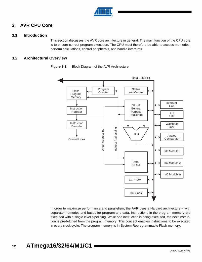
3. AVR CPU Core
3.1 IntroductionThis section discusses the AVR core architecture in general. The main function of the CPU coreis to ensure correct program execution. The CPU must therefore be able to access memories,perform calculations, control peripherals, and handle interrupts.
3.2 Architectural Overview
Figure 3-1. Block Diagram of the AVR Architecture
In order to maximize performance and parallelism, the AVR uses a Harvard architecture – withseparate memories and buses for program and data. Instructions in the program memory areexecuted with a single level pipelining. While one instruction is being executed, the next instruc-tion is pre-fetched from the program memory. This concept enables instructions to be executedin every clock cycle. The program memory is In-System Reprogrammable Flash memory.
FlashProgramMemory
InstructionRegister
InstructionDecoder
ProgramCounter
Control Lines
32 x 8GeneralPurpose
Registrers
ALU
Statusand Control
I/O Lines
EEPROM
Data Bus 8-bit
DataSRAM
Dire
ct A
ddre
ssin
g
Indi
rect
Add
ress
ing
InterruptUnit
SPIUnit
WatchdogTimer
AnalogComparator
I/O Module 2
I/O Module1
I/O Module n
127647C–AVR–07/08
ATmega16/32/64/M1/C1

ATmega16/32/64/M1/C1
The fast-access Register File contains 32 x 8-bit general purpose working registers with a singleclock cycle access time. This allows single-cycle Arithmetic Logic Unit (ALU) operation. In a typ-ical ALU operation, two operands are output from the Register File, the operation is executed,and the result is stored back in the Register File – in one clock cycle.
Six of the 32 registers can be used as three 16-bit indirect address register pointers for DataSpace addressing – enabling efficient address calculations. One of the these address pointerscan also be used as an address pointer for look up tables in Flash program memory. Theseadded function registers are the 16-bit X-, Y-, and Z-register, described later in this section.
The ALU supports arithmetic and logic operations between registers or between a constant anda register. Single register operations can also be executed in the ALU. After an arithmetic opera-tion, the Status Register is updated to reflect information about the result of the operation.
Program flow is provided by conditional and unconditional jump and call instructions, able todirectly address the whole address space. Most AVR instructions have a single 16-bit word for-mat. Every program memory address contains a 16- or 32-bit instruction.
Program Flash memory space is divided in two sections, the Boot Program section and theApplication Program section. Both sections have dedicated Lock bits for write and read/writeprotection. The SPM (Store Program Memory) instruction that writes into the Application Flashmemory section must reside in the Boot Program section.
During interrupts and subroutine calls, the return address Program Counter (PC) is stored on theStack. The Stack is effectively allocated in the general data SRAM, and consequently the Stacksize is only limited by the total SRAM size and the usage of the SRAM. All user programs mustinitialize the SP in the Reset routine (before subroutines or interrupts are executed). The StackPointer (SP) is read/write accessible in the I/O space. The data SRAM can easily be accessedthrough the five different addressing modes supported in the AVR architecture.
The memory spaces in the AVR architecture are all linear and regular memory maps.
A flexible interrupt module has its control registers in the I/O space with an additional GlobalInterrupt Enable bit in the Status Register. All interrupts have a separate Interrupt Vector in theInterrupt Vector table. The interrupts have priority in accordance with their Interrupt Vector posi-tion. The lower the Interrupt Vector address, the higher is the priority.
The I/O memory space contains 64 addresses for CPU peripheral functions as Control Regis-ters, SPI, and other I/O functions. The I/O Memory can be accessed directly, or as the DataSpace locations following those of the Register File, 0x20 - 0x5F. In addition, theATmega16/32/64/M1/C1 has Extended I/O space from 0x60 - 0xFF in SRAM where only theST/STS/STD and LD/LDS/LDD instructions can be used.
3.3 ALU – Arithmetic Logic UnitThe high-performance AVR ALU operates in direct connection with all the 32 general purposeworking registers. Within a single clock cycle, arithmetic operations between general purposeregisters or between a register and an immediate are executed. The ALU operations are dividedinto three main categories – arithmetic, logical, and bit-functions. Some implementations of thearchitecture also provide a powerful multiplier supporting both signed/unsigned multiplicationand fractional format. See the “Instruction Set” section for a detailed description.
137647C–AVR–07/08

3.4 Status RegisterThe Status Register contains information about the result of the most recently executed arith-metic instruction. This information can be used for altering program flow in order to performconditional operations. Note that the Status Register is updated after all ALU operations, asspecified in the Instruction Set Reference. This will in many cases remove the need for using thededicated compare instructions, resulting in faster and more compact code.
The Status Register is not automatically stored when entering an interrupt routine and restoredwhen returning from an interrupt. This must be handled by software.
The AVR Status Register – SREG – is defined as:
• Bit 7 – I: Global Interrupt EnableThe Global Interrupt Enable bit must be set to enabled the interrupts. The individual interruptenable control is then performed in separate control registers. If the Global Interrupt EnableRegister is cleared, none of the interrupts are enabled independent of the individual interruptenable settings. The I-bit is cleared by hardware after an interrupt has occurred, and is set bythe RETI instruction to enable subsequent interrupts. The I-bit can also be set and cleared bythe application with the SEI and CLI instructions, as described in the instruction set reference.
• Bit 6 – T: Bit Copy StorageThe Bit Copy instructions BLD (Bit LoaD) and BST (Bit STore) use the T-bit as source or desti-nation for the operated bit. A bit from a register in the Register File can be copied into T by theBST instruction, and a bit in T can be copied into a bit in a register in the Register File by theBLD instruction.
• Bit 5 – H: Half Carry Flag The Half Carry Flag H indicates a Half Carry in some arithmetic operations. Half Carry Is usefulin BCD arithmetic. See the “Instruction Set Description” for detailed information.
• Bit 4 – S: Sign Bit, S = N ⊕ VThe S-bit is always an exclusive or between the negative flag N and the Two’s ComplementOverflow Flag V. See the “Instruction Set Description” for detailed information.
• Bit 3 – V: Two’s Complement Overflow FlagThe Two’s Complement Overflow Flag V supports two’s complement arithmetics. See the“Instruction Set Description” for detailed information.
• Bit 2 – N: Negative FlagThe Negative Flag N indicates a negative result in an arithmetic or logic operation. See the“Instruction Set Description” for detailed information.
• Bit 1 – Z: Zero FlagThe Zero Flag Z indicates a zero result in an arithmetic or logic operation. See the “InstructionSet Description” for detailed information.
Bit 7 6 5 4 3 2 1 0
I T H S V N Z C SREGRead/Write R/W R/W R/W R/W R/W R/W R/W R/W
Initial Value 0 0 0 0 0 0 0 0
147647C–AVR–07/08
ATmega16/32/64/M1/C1

ATmega16/32/64/M1/C1
• Bit 0 – C: Carry FlagThe Carry Flag C indicates a carry in an arithmetic or logic operation. See the “Instruction SetDescription” for detailed information.
3.5 General Purpose Register FileThe Register File is optimized for the AVR Enhanced RISC instruction set. In order to achievethe required performance and flexibility, the following input/output schemes are supported by theRegister File:
• One 8-bit output operand and one 8-bit result input• Two 8-bit output operands and one 8-bit result input• Two 8-bit output operands and one 16-bit result input• One 16-bit output operand and one 16-bit result input
Figure 3-2 shows the structure of the 32 general purpose working registers in the CPU.
Figure 3-2. AVR CPU General Purpose Working Registers
Most of the instructions operating on the Register File have direct access to all registers, andmost of them are single cycle instructions.
As shown in Figure 3-2, each register is also assigned a data memory address, mapping themdirectly into the first 32 locations of the user Data Space. Although not being physically imple-mented as SRAM locations, this memory organization provides great flexibility in access of theregisters, as the X-, Y- and Z-pointer registers can be set to index any register in the file.
3.5.1 The X-register, Y-register, and Z-registerThe registers R26..R31 have some added functions to their general purpose usage. These reg-isters are 16-bit address pointers for indirect addressing of the data space. The three indirectaddress registers X, Y, and Z are defined as described in Figure 3-3.
7 0 Addr.
R0 0x00
R1 0x01
R2 0x02
…
R13 0x0D
General R14 0x0E
Purpose R15 0x0F
Working R16 0x10
Registers R17 0x11
…
R26 0x1A X-register Low Byte
R27 0x1B X-register High Byte
R28 0x1C Y-register Low Byte
R29 0x1D Y-register High Byte
R30 0x1E Z-register Low Byte
R31 0x1F Z-register High Byte
157647C–AVR–07/08

Figure 3-3. The X-, Y-, and Z-registers
In the different addressing modes these address registers have functions as fixed displacement,automatic increment, and automatic decrement (see the instruction set reference for details).
3.6 Stack PointerThe Stack is mainly used for storing temporary data, for storing local variables and for storingreturn addresses after interrupts and subroutine calls. The Stack Pointer Register always pointsto the top of the Stack. Note that the Stack is implemented as growing from higher memory loca-tions to lower memory locations. This implies that a Stack PUSH command decreases the StackPointer.
The Stack Pointer points to the data SRAM Stack area where the Subroutine and InterruptStacks are located. This Stack space in the data SRAM must be defined by the program beforeany subroutine calls are executed or interrupts are enabled. The Stack Pointer must be set topoint above 0x100. The Stack Pointer is decremented by one when data is pushed onto theStack with the PUSH instruction, and it is decremented by two when the return address ispushed onto the Stack with subroutine call or interrupt. The Stack Pointer is incremented by onewhen data is popped from the Stack with the POP instruction, and it is incremented by two whendata is popped from the Stack with return from subroutine RET or return from interrupt RETI.
The AVR Stack Pointer is implemented as two 8-bit registers in the I/O space. The number ofbits actually used is implementation dependent. Note that the data space in some implementa-tions of the AVR architecture is so small that only SPL is needed. In this case, the SPH Registerwill not be present.
3.7 Instruction Execution TimingThis section describes the general access timing concepts for instruction execution. The AVRCPU is driven by the CPU clock clkCPU, directly generated from the selected clock source for thechip. No internal clock division is used.
15 XH XL 0
X-register 7 0 7 0
R27 (0x1B) R26 (0x1A)
15 YH YL 0
Y-register 7 0 7 0
R29 (0x1D) R28 (0x1C)
15 ZH ZL 0
Z-register 7 0 7 0
R31 (0x1F) R30 (0x1E)
Bit 15 14 13 12 11 10 9 8
SP15 SP14 SP13 SP12 SP11 SP10 SP9 SP8 SPHSP7 SP6 SP5 SP4 SP3 SP2 SP1 SP0 SPL7 6 5 4 3 2 1 0
Read/Write R/W R/W R/W R/W R/W R/W R/W R/W
R/W R/W R/W R/W R/W R/W R/W R/W
Initial Value 0 0 0 0 0 0 0 0
0 0 0 0 0 0 0 0
167647C–AVR–07/08
ATmega16/32/64/M1/C1

ATmega16/32/64/M1/C1
Figure 3-4 shows the parallel instruction fetches and instruction executions enabled by the Har-vard architecture and the fast-access Register File concept. This is the basic pipelining conceptto obtain up to 1 MIPS per MHz with the corresponding unique results for functions per cost,functions per clocks, and functions per power-unit.
Figure 3-4. The Parallel Instruction Fetches and Instruction Executions
Figure 3-5 shows the internal timing concept for the Register File. In a single clock cycle an ALUoperation using two register operands is executed, and the result is stored back to the destina-tion register.
Figure 3-5. Single Cycle ALU Operation
3.8 Reset and Interrupt HandlingThe AVR provides several different interrupt sources. These interrupts and the separate ResetVector each have a separate program vector in the program memory space. All interrupts areassigned individual enable bits which must be written logic one together with the Global InterruptEnable bit in the Status Register in order to enable the interrupt. Depending on the ProgramCounter value, interrupts may be automatically disabled when Boot Lock bits BLB02 or BLB12are programmed. This feature improves software security. See the section “Memory Program-ming” on page 294 for details.
The lowest addresses in the program memory space are by default defined as the Reset andInterrupt Vectors. The complete list of vectors is shown in “Interrupts” on page 56. The list alsodetermines the priority levels of the different interrupts. The lower the address the higher is thepriority level. RESET has the highest priority, and next is ANACOMP0 – the Analog Comparator0 Interrupt. The Interrupt Vectors can be moved to the start of the Boot Flash section by settingthe IVSEL bit in the MCU Control Register (MCUCR). Refer to “Interrupts” on page 56 for moreinformation. The Reset Vector can also be moved to the start of the Boot Flash section by pro-
clk
1st Instruction Fetch
1st Instruction Execute2nd Instruction Fetch
2nd Instruction Execute3rd Instruction Fetch
3rd Instruction Execute4th Instruction Fetch
T1 T2 T3 T4
CPU
Total Execution Time
Register Operands Fetch
ALU Operation Execute
Result Write Back
T1 T2 T3 T4
clkCPU
177647C–AVR–07/08

gramming the BOOTRST Fuse, see “Boot Loader Support – Read-While-Write Self-Programming ATmega16/32/64/M1/C1” on page 275.
3.8.1 Interrupt BehaviorWhen an interrupt occurs, the Global Interrupt Enable I-bit is cleared and all interrupts are dis-abled. The user software can write logic one to the I-bit to enable nested interrupts. All enabledinterrupts can then interrupt the current interrupt routine. The I-bit is automatically set when aReturn from Interrupt instruction – RETI – is executed.
There are basically two types of interrupts. The first type is triggered by an event that sets theinterrupt flag. For these interrupts, the Program Counter is vectored to the actual Interrupt Vectorin order to execute the interrupt handling routine, and hardware clears the corresponding inter-rupt flag. Interrupt flags can also be cleared by writing a logic one to the flag bit position(s) to becleared. If an interrupt condition occurs while the corresponding interrupt enable bit is cleared,the interrupt flag will be set and remembered until the interrupt is enabled, or the flag is clearedby software. Similarly, if one or more interrupt conditions occur while the Global Interrupt Enablebit is cleared, the corresponding interrupt flag(s) will be set and remembered until the GlobalInterrupt Enable bit is set, and will then be executed by order of priority.
The second type of interrupts will trigger as long as the interrupt condition is present. Theseinterrupts do not necessarily have interrupt flags. If the interrupt condition disappears before theinterrupt is enabled, the interrupt will not be triggered.
When the AVR exits from an interrupt, it will always return to the main program and execute onemore instruction before any pending interrupt is served.
Note that the Status Register is not automatically stored when entering an interrupt routine, norrestored when returning from an interrupt routine. This must be handled by software.
When using the CLI instruction to disable interrupts, the interrupts will be immediately disabled.No interrupt will be executed after the CLI instruction, even if it occurs simultaneously with theCLI instruction. The following example shows how this can be used to avoid interrupts during thetimed EEPROM write sequence..
Assembly Code Examplein r16, SREG ; store SREG value
cli ; disable interrupts during timed sequence
sbi EECR, EEMWE ; start EEPROM write
sbi EECR, EEWE
out SREG, r16 ; restore SREG value (I-bit)
C Code Examplechar cSREG;
cSREG = SREG; /* store SREG value */
/* disable interrupts during timed sequence */
_CLI();
EECR |= (1<<EEMWE); /* start EEPROM write */
EECR |= (1<<EEWE);
SREG = cSREG; /* restore SREG value (I-bit) */
187647C–AVR–07/08
ATmega16/32/64/M1/C1

ATmega16/32/64/M1/C1
When using the SEI instruction to enable interrupts, the instruction following SEI will be exe-cuted before any pending interrupts, as shown in this example.
3.8.2 Interrupt Response TimeThe interrupt execution response for all the enabled AVR interrupts is four clock cycles mini-mum. After four clock cycles the program vector address for the actual interrupt handling routineis executed. During this four clock cycle period, the Program Counter is pushed onto the Stack.The vector is normally a jump to the interrupt routine, and this jump takes three clock cycles. Ifan interrupt occurs during execution of a multi-cycle instruction, this instruction is completedbefore the interrupt is served. If an interrupt occurs when the MCU is in sleep mode, the interruptexecution response time is increased by four clock cycles. This increase comes in addition to thestart-up time from the selected sleep mode.
A return from an interrupt handling routine takes four clock cycles. During these four clockcycles, the Program Counter (two bytes) is popped back from the Stack, the Stack Pointer isincremented by two, and the I-bit in SREG is set.
Assembly Code Examplesei ; set Global Interrupt Enable
sleep; enter sleep, waiting for interrupt
; note: will enter sleep before any pending
; interrupt(s)
C Code Example_SEI(); /* set Global Interrupt Enable */
_SLEEP(); /* enter sleep, waiting for interrupt */
/* note: will enter sleep before any pending interrupt(s) */
197647C–AVR–07/08

4. MemoriesThis section describes the different memories in the ATmega16/32/64/M1/C1. The AVR archi-tecture has two main memory spaces, the Data Memory and the Program Memory space. Inaddition, the ATmega16/32/64/M1/C1 features an EEPROM Memory for data storage. All threememory spaces are linear and regular.
4.1 In-System Reprogrammable Flash Program Memory The ATmega16/32/64/M1/C1 contains 16K/32K/64K bytes On-chip In-System ReprogrammableFlash memory for program storage. Since all AVR instructions are 16 or 32 bits wide, the Flashis organized as 8K x 16, 16K x 16 , 32K x 16. For software security, the Flash Program memoryspace is divided into two sections, Boot Program section and Application Program section.
The Flash memory has an endurance of at least 10,000 wri te/erase cycles. TheATmega16/32/64/M1/C1 Program Counter (PC) is 14/15 bits wide, thus addressing the8K/16K/32K program memory locations. The operation of Boot Program section and associatedBoot Lock bits for software protection are described in detail in “Boot Loader Support – Read-While-Write Self-Programming ATmega16/32/64/M1/C1” on page 275. “Memory Programming”on page 294 contains a detailed description on Flash programming in SPI or Parallel program-ming mode.
Constant tables can be allocated within the entire program memory address space (see the LPM– Load Program Memory.
Timing diagrams for instruction fetch and execution are presented in “Instruction Execution Tim-ing” on page 16.
Figure 4-1. Program Memory Map
0x0000
0x1FFF/0x3FFF/0x7FF
Program Memory
Application Flash Section
Boot Flash Section
207647C–AVR–07/08
ATmega16/32/64/M1/C1

ATmega16/32/64/M1/C1
4.2 SRAM Data MemoryFigure 4-2 shows how the ATmega16/32/64/M1/C1 SRAM Memory is organized.
The ATmega16/32/64/M1/C1 is a complex microcontroller with more peripheral units than canbe supported within the 64 locations reserved in the Opcode for the IN and OUT instructions. Forthe Extended I/O space from 0x60 - 0xFF in SRAM, only the ST/STS/STD and LD/LDS/LDDinstructions can be used.
The lower 2304 data memory locations address both the Register File, the I/O memory,Extended I/O memory, and the internal data SRAM. The first 32 locations address the RegisterFile, the next 64 location the standard I/O memory, then 160 locations of Extended I/O memory,and the next 1024/2048/4096 locations address the internal data SRAM.
The five different addressing modes for the data memory cover: Direct, Indirect with Displace-ment, Indirect, Indirect with Pre-decrement, and Indirect with Post-increment. In the RegisterFile, registers R26 to R31 feature the indirect addressing pointer registers.
The direct addressing reaches the entire data space.
The Indirect with Displacement mode reaches 63 address locations from the base address givenby the Y- or Z-register.
When using register indirect addressing modes with automatic pre-decrement and post-incre-ment, the address registers X, Y, and Z are decremented or incremented.
The 32 general purpose working registers, 64 I/O Registers, 160 Extended I/O Registers, andthe 1024/2048/4096 bytes of internal data SRAM in the ATmega16/32/64/M1/C1 are all accessi-ble through all these addressing modes. The Register File is described in “General PurposeRegister File” on page 15.
Figure 4-2. Data Memory Map for 1024/2048/4096 Internal SRAM
4.2.1 SRAM Data Access Times
This section describes the general access timing concepts for internal memory access. Theinternal data SRAM access is performed in two clkCPU cycles as described in Figure 4-3.
FFF
32 Registers64 I/O Registers
Internal SRAM (1024x8) (2048x8) (4096x8)
0x0000 - 0x001F0x0020 - 0x005F
0x04FF/0x08FF/0x10F
0x0060 - 0x00FF
Data Memory
160 Ext I/O Reg.0x0100
217647C–AVR–07/08

Figure 4-3. On-chip Data SRAM Access Cycles
4.3 EEPROM Data MemoryThe ATmega16/32/64/M1/C1 contains 512/1024/2048 bytes of data EEPROM memory. It isorganized as a separate data space, in which single bytes can be read and written. TheEEPROM has an endurance of at least 100,000 write/erase cycles. The access between theEEPROM and the CPU is described in the following, specifying the EEPROM Address Regis-ters, the EEPROM Data Register, and the EEPROM Control Register.
For a detailed description of SPI and Parallel data downloading to the EEPROM, see “SerialDownloading” on page 310 , and “Parallel Programming Parameters, Pin Mapping, and Com-mands” on page 298 respectively.
4.3.1 EEPROM Read/Write Access
The EEPROM Access Registers are accessible in the I/O space.
The write access time for the EEPROM is given in Table 4-2. A self-timing function, however,lets the user software detect when the next byte can be written. If the user code contains instruc-tions that write the EEPROM, some precautions must be taken. In heavily filtered powersupplies, VCC is likely to rise or fall slowly on power-up/down. This causes the device for someperiod of time to run at a voltage lower than specified as minimum for the clock frequency used.See “Preventing EEPROM Corruption” on page 27.for details on how to avoid problems in thesesituations.
In order to prevent unintentional EEPROM writes, a specific write procedure must be followed.Refer to the description of the EEPROM Control Register for details on this.
When the EEPROM is read, the CPU is halted for four clock cycles before the next instruction isexecuted. When the EEPROM is written, the CPU is halted for two clock cycles before the nextinstruction is executed.
clk
WR
RD
Data
Data
Address Address valid
T1 T2 T3
Compute Address
Rea
dW
rite
CPU
Memory Access Instruction Next Instruction
227647C–AVR–07/08
ATmega16/32/64/M1/C1
ATmega16/32/64/M1/C1
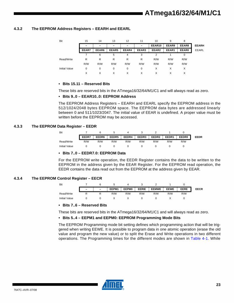
4.3.2 The EEPROM Address Registers – EEARH and EEARL
• Bits 15.11 – Reserved Bits
These bits are reserved bits in the ATmega16/32/64/M1/C1 and will always read as zero.• Bits 9..0 – EEAR10..0: EEPROM Address
The EEPROM Address Registers – EEARH and EEARL specify the EEPROM address in the512/1024/2048 bytes EEPROM space. The EEPROM data bytes are addressed linearlybetween 0 and 511/1023/2047. The initial value of EEAR is undefined. A proper value must bewritten before the EEPROM may be accessed.
4.3.3 The EEPROM Data Register – EEDR
• Bits 7..0 – EEDR7.0: EEPROM Data
For the EEPROM write operation, the EEDR Register contains the data to be written to theEEPROM in the address given by the EEAR Register. For the EEPROM read operation, theEEDR contains the data read out from the EEPROM at the address given by EEAR.
4.3.4 The EEPROM Control Register – EECR
• Bits 7..6 – Reserved Bits
These bits are reserved bits in the ATmega16/32/64/M1/C1 and will always read as zero.• Bits 5..4 – EEPM1 and EEPM0: EEPROM Programming Mode Bits
The EEPROM Programming mode bit setting defines which programming action that will be trig-gered when writing EEWE. It is possible to program data in one atomic operation (erase the oldvalue and program the new value) or to split the Erase and Write operations in two differentoperations. The Programming times for the different modes are shown in Table 4-1. While
Bit 15 14 13 12 11 10 9 8
– – – – – EEAR10 EEAR9 EEAR8 EEARHEEAR7 EEAR6 EEAR5 EEAR4 EEAR3 EEAR2 EEAR1 EEAR0 EEARL
7 6 5 4 3 2 1 0
Read/Write R R R R R R/W R/W R/W
R/W R/W R/W R/W R/W R/W R/W R/W
Initial Value 0 0 0 0 0 X X X
X X X X X X X X
Bit 7 6 5 4 3 2 1 0
EEDR7 EEDR6 EEDR5 EEDR4 EEDR3 EEDR2 EEDR1 EEDR0 EEDRRead/Write R/W R/W R/W R/W R/W R/W R/W R/W
Initial Value 0 0 0 0 0 0 0 0
Bit 7 6 5 4 3 2 1 0
– – EEPM1 EEPM0 EERIE EEMWE EEWE EERE EECRRead/Write R R R/W R/W R/W R/W R/W R/W
Initial Value 0 0 X X 0 0 X 0
237647C–AVR–07/08
EEWE is set, any write to EEPMn will be ignored. During reset, the EEPMn bits will be reset to0b00 unless the EEPROM is busy programming.
• Bit 3 – EERIE: EEPROM Ready Interrupt Enable
Writing EERIE to one enables the EEPROM Ready Interrupt if the I bit in SREG is set. WritingEERIE to zero disables the interrupt. The EEPROM Ready interrupt generates a constant inter-rupt when EEWE is cleared. The interrupt will not be generated during EEPROM write or SPM.• Bit 2 – EEMWE: EEPROM Master Write Enable
The EEMWE bit determines whether setting EEWE to one causes the EEPROM to be written.When EEMWE is set, setting EEWE within four clock cycles will write data to the EEPROM atthe selected address If EEMWE is zero, setting EEWE will have no effect. When EEMWE hasbeen written to one by software, hardware clears the bit to zero after four clock cycles. See thedescription of the EEWE bit for an EEPROM write procedure.• Bit 1 – EEWE: EEPROM Write Enable
The EEPROM Write Enable Signal EEWE is the write strobe to the EEPROM. When addressand data are correctly set up, the EEWE bit must be written to one to write the value into theEEPROM. The EEMWE bit must be written to one before a logical one is written to EEWE, oth-erwise no EEPROM write takes place. The following procedure should be followed when writingthe EEPROM (the order of steps 3 and 4 is not essential):1. Wait until EEWE becomes zero.2. Wait until SPMEN (Store Program Memory Enable) in SPMCSR (Store Program Memory
Control and Status Register) becomes zero.3. Write new EEPROM address to EEAR (optional).4. Write new EEPROM data to EEDR (optional).5. Write a logical one to the EEMWE bit while writing a zero to EEWE in EECR.6. Within four clock cycles after setting EEMWE, write a logical one to EEWE.
The EEPROM can not be programmed during a CPU write to the Flash memory. The softwaremust check that the Flash programming is completed before initiating a new EEPROM write.Step 2 is only relevant if the software contains a Boot Loader allowing the CPU to program theFlash. If the Flash is never being updated by the CPU, step 2 can be omitted. See “Boot LoaderSupport – Read-While-Write Self-Programming ATmega16/32/64/M1/C1” on page 275 fordetails about Boot programming.
Caution: An interrupt between step 5 and step 6 will make the write cycle fail, since theEEPROM Master Write Enable will time-out. If an interrupt routine accessing the EEPROM isinterrupting another EEPROM access, the EEAR or EEDR Register will be modified, causing theinterrupted EEPROM access to fail. It is recommended to have the Global Interrupt Flag clearedduring all the steps to avoid these problems.
Table 4-1. EEPROM Mode Bits
EEPM1 EEPM0Programming
Time Operation
0 0 3.4 ms Erase and Write in one operation (Atomic Operation)
0 1 1.8 ms Erase Only
1 0 1.8 ms Write Only
1 1 – Reserved for future use
247647C–AVR–07/08
ATmega16/32/64/M1/C1

ATmega16/32/64/M1/C1
When the write access time has elapsed, the EEWE bit is cleared by hardware. The user soft-ware can poll this bit and wait for a zero before writing the next byte. When EEWE has been set,the CPU is halted for two cycles before the next instruction is executed.• Bit 0 – EERE: EEPROM Read Enable
The EEPROM Read Enable Signal EERE is the read strobe to the EEPROM. When the correctaddress is set up in the EEAR Register, the EERE bit must be written to a logic one to trigger theEEPROM read. The EEPROM read access takes one instruction, and the requested data isavailable immediately. When the EEPROM is read, the CPU is halted for four cycles before thenext instruction is executed.
The user should poll the EEWE bit before starting the read operation. If a write operation is inprogress, it is neither possible to read the EEPROM, nor to change the EEAR Register.
The calibrated Oscillator is used to time the EEPROM accesses. Table 4-2 lists the typical pro-gramming time for EEPROM access from the CPU.
The following code examples show one assembly and one C function for writing to theEEPROM. The examples assume that interrupts are controlled (e.g. by disabling interrupts glo-bally) so that no interrupts will occur during execution of these functions. The examples alsoassume that no Flash Boot Loader is present in the software. If such code is present, theEEPROM write function must also wait for any ongoing SPM command to finish.
Table 4-2. EEPROM Programming Time.
Symbol Number of Calibrated RC Oscillator Cycles Typ Programming Time
EEPROM write (from CPU) 26368 3.3 ms
257647C–AVR–07/08

Assembly Code Example
EEPROM_write:
; Wait for completion of previous write
sbic EECR,EEWE
rjmp EEPROM_write
; Set up address (r18:r17) in address register
out EEARH, r18
out EEARL, r17
; Write data (r16) to data register
out EEDR,r16
; Write logical one to EEMWE
sbi EECR,EEMWE
; Start eeprom write by setting EEWE
sbi EECR,EEWE
ret
C Code Example
void EEPROM_write (unsigned int uiAddress, unsigned char ucData)
{
/* Wait for completion of previous write */
while(EECR & (1<<EEWE))
;
/* Set up address and data registers */
EEAR = uiAddress;
EEDR = ucData;
/* Write logical one to EEMWE */
EECR |= (1<<EEMWE);
/* Start eeprom write by setting EEWE */
EECR |= (1<<EEWE);
}
267647C–AVR–07/08
ATmega16/32/64/M1/C1

ATmega16/32/64/M1/C1
The next code examples show assembly and C functions for reading the EEPROM. The exam-ples assume that interrupts are controlled so that no interrupts will occur during execution ofthese functions.
4.3.5 Preventing EEPROM Corruption
During periods of low VCC, the EEPROM data can be corrupted because the supply voltage istoo low for the CPU and the EEPROM to operate properly. These issues are the same as forboard level systems using EEPROM, and the same design solutions should be applied.
An EEPROM data corruption can be caused by two situations when the voltage is too low. First,a regular write sequence to the EEPROM requires a minimum voltage to operate correctly. Sec-ondly, the CPU itself can execute instructions incorrectly, if the supply voltage is too low.
EEPROM data corruption can easily be avoided by following this design recommendation:
Keep the AVR RESET active (low) during periods of insufficient power supply voltage. This canbe done by enabling the internal Brown-out Detector (BOD). If the detection level of the internalBOD does not match the needed detection level, an external low VCC reset Protection circuit canbe used. If a reset occurs while a write operation is in progress, the write operation will be com-pleted provided that the power supply voltage is sufficient.
Assembly Code Example
EEPROM_read:
; Wait for completion of previous write
sbic EECR,EEWE
rjmp EEPROM_read
; Set up address (r18:r17) in address register
out EEARH, r18
out EEARL, r17
; Start eeprom read by writing EERE
sbi EECR,EERE
; Read data from data register
in r16,EEDR
ret
C Code Example
unsigned char EEPROM_read(unsigned int uiAddress)
{
/* Wait for completion of previous write */
while(EECR & (1<<EEWE))
;
/* Set up address register */
EEAR = uiAddress;
/* Start eeprom read by writing EERE */
EECR |= (1<<EERE);
/* Return data from data register */
return EEDR;
}
277647C–AVR–07/08

4.4 I/O MemoryThe I/O space definition of the ATmega16/32/64/M1/C1 is shown in “Register Summary” onpage 351.
All ATmega16/32/64/M1/C1 I/Os and peripherals are placed in the I/O space. All I/O locationsmay be accessed by the LD/LDS/LDD and ST/STS/STD instructions, transferring data betweenthe 32 general purpose working registers and the I/O space. I/O registers within the addressrange 0x00 - 0x1F are directly bit-accessible using the SBI and CBI instructions. In these regis-ters, the value of single bits can be checked by using the SBIS and SBIC instructions. Refer tothe instruction set section for more details. When using the I/O specific commands IN and OUT,the I/O addresses 0x00 - 0x3F must be used. When addressing I/O registers as data spaceus ing LD and ST ins t ruc t ions , 0x20 mus t be added to these addresses . TheATmega16/32/64/M1/C1 is a complex microcontroller with more peripheral units than can besupported within the 64 location reserved in Opcode for the IN and OUT instructions. For theExtended I/O space from 0x60 - 0xFF in SRAM, only the ST/STS/STD and LD/LDS/LDD instruc-tions can be used.
For compatibility with future devices, reserved bits should be written to zero if accessed.Reserved I/O memory addresses should never be written.
Some of the status flags are cleared by writing a logical one to them. Note that, unlike most otherAVR’s, the CBI and SBI instructions will only operate on the specified bit, and can therefore beused on registers containing such status flags. The CBI and SBI instructions work with registers0x00 to 0x1F only.
The I/O and peripherals control registers are explained in later sections.
4.5 General Purpose I/O RegistersThe ATmega16/32/64/M1/C1 contains four General Purpose I/O Registers. These registers canbe used for storing any information, and they are particularly useful for storing global variablesand status flags.
The General Purpose I/O Registers, within the address range 0x00 - 0x1F, are directly bit-accessible using the SBI, CBI, SBIS, and SBIC instructions.
4.5.1 General Purpose I/O Register 0 – GPIOR0
4.5.2 General Purpose I/O Register 1 – GPIOR1
4.5.3 General Purpose I/O Register 2 – GPIOR2
Bit 7 6 5 4 3 2 1 0
GPIOR07 GPIOR06 GPIOR05 GPIOR04 GPIOR03 GPIOR02 GPIOR01 GPIOR00 GPIOR0Read/Write R/W R/W R/W R/W R/W R/W R/W R/W
Initial Value 0 0 0 0 0 0 0 0
Bit 7 6 5 4 3 2 1 0
GPIOR17 GPIOR16 GPIOR15 GPIOR14 GPIOR13 GPIOR12 GPIOR11 GPIOR10 GPIOR1Read/Write R/W R/W R/W R/W R/W R/W R/W R/W
Initial Value 0 0 0 0 0 0 0 0
Bit 7 6 5 4 3 2 1 0
GPIOR27 GPIOR26 GPIOR25 GPIOR24 GPIOR23 GPIOR22 GPIOR21 GPIOR20 GPIOR2Read/Write R/W R/W R/W R/W R/W R/W R/W R/W
Initial Value 0 0 0 0 0 0 0 0
287647C–AVR–07/08
ATmega16/32/64/M1/C1

ATmega16/32/64/M1/C1
5. System Clock
5.1 Clock Systems and their DistributionFigure 5-1 presents the principal clock systems in the AVR and their distribution. All of the clocksneed not be active at a given time. In order to reduce power consumption, the clocks to unusedmodules can be halted by using different sleep modes, as described in “Power Management andSleep Modes” on page 40. The clock systems are detailed below.
Figure 5-1. Clock Distribution
5.1.1 CPU Clock – clkCPU
The CPU clock is routed to parts of the system concerned with operation of the AVR core.Examples of such modules are the General Purpose Register File, the Status Register and thedata memory holding the Stack Pointer. Halting the CPU clock inhibits the core from performinggeneral operations and calculations.
5.1.2 I/O Clock – clkI/O
The I/O clock is used by the majority of the I/O modules, like Timer/Counters, SPI, UART. TheI/O clock is also used by the External Interrupt module, but note that some external interruptsare detected by asynchronous logic, allowing such interrupts to be detected even if the I/O clockis halted.
General I/OModules
ADC CPU Core RAM
clk I/O AVR ClockControl Unit
clk CPU
Flash andEEPROM
clk FLASH
clk ADC
Source Clock
Watchdog Timer
WatchdogOscillator
Reset Logic
ClockMultiplexer
Watchdog Clock
Calibrated RCOscillator
(CrystalOscillator)
External Clock
Fast Peripherals
PLL
CLK PLL
MultiplexerPLL Input
297647C–AVR–07/08
5.1.3 Flash Clock – clkFLASH
The Flash clock controls operation of the Flash interface. The Flash clock is usually active simul-taneously with the CPU clock.
5.1.4 PLL Clock – clkPLL
The PLL clock allows the fast peripherals to be clocked directly from a 64/32 MHz clock. A 16MHz clock is also derived for the CPU.
5.1.5 ADC Clock – clkADC
The ADC is provided with a dedicated clock domain. This allows halting the CPU and I/O clocksin order to reduce noise generated by digital circuitry. This gives more accurate ADC conversionresults.
5.2 Clock SourcesThe device has the following clock source options, selectable by Flash Fuse bits as illustratedTable 5-1. The clock from the selected source is input to the AVR clock generator, and routed tothe appropriate modules.
Note: 1. For all fuses “1” means unprogrammed while “0” means programmed.2. Ext Osc : External Osc3. RC Osc : Internal RC Oscillator4. Ext Clk : External Clock Input
The various choices for each clocking option is given in the following sections. When the CPUwakes up from Power-down or Power-save, the selected clock source is used to time the start-up, ensuring stable Oscillator operation before instruction execution starts. When the CPU startsfrom reset, there is an additional delay allowing the power to reach a stable level before startingnormal operation. The Watchdog Oscillator is used for timing this real-time part of the start-uptime. The number of WDT Oscillator cycles used for each time-out is shown in Table 5-2. The
Table 5-1. Device Clocking Options Select(1)
Device Clocking Option System Clock PLL Input
CKSEL3..0
External Crystal/Ceramic Resonator Ext Osc RC Osc 1111 - 1000
PLL output divided by 4 : 16 MHz / PLL driven by External Crystal/Ceramic Resonator Ext Osc Ext Osc 0100
PLL output divided by 4 : 16 MHz / PLL driven by External Crystal/Ceramic Resonator PLL / 4 Ext Osc 0101
Reserved N/A N/A 0110
Reserved N/A N/A 0111
PLL output divided by 4 : 16 MHz PLL / 4 RC Osc 0011
Calibrated Internal RC Oscillator RC Osc RC Osc 0010
PLL output divided by 4 : 16 MHz / PLL driven by External clock PLL / 4 Ext Clk 0001
External Clock Ext Clk RC Osc 0000
307647C–AVR–07/08
ATmega16/32/64/M1/C1

ATmega16/32/64/M1/C1
frequency of the Watchdog Oscillator is voltage dependent as shown in “Watchdog OscillatorFrequency vs. VCC” on page 344.
5.3 Default Clock SourceThe device is shipped with CKSEL = “0010”, SUT = “10”, and CKDIV8 programmed. The defaultclock source setting is the Internal RC Oscillator with longest start-up time and an initial systemclock prescaling of 8. This default setting ensures that all users can make their desired clocksource setting using an In-System or Parallel programmer.
5.4 Low Power Crystal OscillatorXTAL1 and XTAL2 are input and output, respectively, of an inverting amplifier which can be con-figured for use as an On-chip Oscillator, as shown in Figure 5-2. Either a quartz crystal or aceramic resonator may be used.
This Crystal Oscillator is a low power oscillator, with reduced voltage swing on the XTAL2 out-put. It gives the lowest power consumption, but is not capable of driving other clock inputs.
C1 and C2 should always be equal for both crystals and resonators. The optimal value of thecapacitors depends on the crystal or resonator in use, the amount of stray capacitance, and theelectromagnetic noise of the environment. Some initial guidelines for choosing capacitors foruse with crystals are given in Table 5-3. For ceramic resonators, the capacitor values given bythe manufacturer should be used. For more information on how to choose capacitors and otherdetails on Oscillator operation, refer to the Multi-purpose Oscillator Application Note.
Figure 5-2. Crystal Oscillator Connections
The Oscillator can operate in three different modes, each optimized for a specific frequencyrange. The operating mode is selected by the fuses CKSEL3..1 as shown in Table 5-3.
Table 5-2. Number of Watchdog Oscillator Cycles
Typ Time-out (VCC = 5.0V) Typ Time-out (VCC = 3.0V) Number of Cycles
4.1 ms 4.3 ms 4K (4,096)
65 ms 69 ms 64K (65,536)
Table 5-3. Crystal Oscillator Operating Modes
CKSEL3..1 Frequency Range(1) (MHz)Recommended Range for Capacitors C1 and
C2 for Use with Crystals (pF)
100(2) 0.4 - 0.9 –
XTAL2
XTAL1
GND
C2
C1
317647C–AVR–07/08
Notes: 1. The frequency ranges are preliminary values. Actual values are TBD.2. This option should not be used with crystals, only with ceramic resonators.
The CKSEL0 Fuse together with the SUT1..0 Fuses select the start-up times as shown in Table5-4.
Notes: 1. These options should only be used when not operating close to the maximum frequency of thedevice, and only if frequency stability at start-up is not important for the application. Theseoptions are not suitable for crystals.
2. These options are intended for use with ceramic resonators and will ensure frequency stabilityat start-up. They can also be used with crystals when not operating close to the maximum fre-quency of the device, and if frequency stability at start-up is not important for the application.
5.5 Calibrated Internal RC OscillatorBy default, the Internal RC OScillator provides an approximate 8.0 MHz clock. Though voltageand temperature dependent, this clock can be very accurately calibrated by the user. The deviceis shipped with the CKDIV8 Fuse programmed. See “System Clock Prescaler” on page 37 formore details.
This clock may be selected as the system clock by programming the CKSEL Fuses as shown inTable 5-1. If selected, it will operate with no external components. During reset, hardware loadsthe pre-programmed calibration value into the OSCCAL Register and thereby automatically cal-
101 0.9 - 3.0 12 - 22
110 3.0 - 8.0 12 - 22
111 8.0 -16.0 12 - 22
Table 5-4. Start-up Times for the Oscillator Clock Selection
CKSEL0 SUT1..0
Start-up Time from Power-down and
Power-save
Additional Delay from Reset (VCC = 5.0V) Recommended Usage
0 00 258 CK(1) 14CK + 4.1 ms Ceramic resonator, fast rising power
0 01 258 CK(1) 14CK + 65 ms Ceramic resonator, slowly rising power
0 10 1K CK(2) 14CK Ceramic resonator, BOD enabled
0 11 1K CK(2) 14CK + 4.1 ms Ceramic resonator, fast rising power
1 00 1K CK(2) 14CK + 65 ms Ceramic resonator, slowly rising power
1 01 16K CK 14CK Crystal Oscillator, BOD enabled
1 10 16K CK 14CK + 4.1 ms Crystal Oscillator, fast rising power
1 11 16K CK 14CK + 65 ms Crystal Oscillator, slowly rising power
Table 5-3. Crystal Oscillator Operating Modes
CKSEL3..1 Frequency Range(1) (MHz)Recommended Range for Capacitors C1 and
C2 for Use with Crystals (pF)
327647C–AVR–07/08
ATmega16/32/64/M1/C1

ATmega16/32/64/M1/C1
ibrates the RC Oscillator. The accuracy of this calibration is shown as Factory calibration inTable 26-1 on page 317.
By changing the OSCCAL register from SW, see “Oscillator Calibration Register – OSCCAL” onpage 33, it is possible to get a higher calibration accuracy than by using the factory calibration.The accuracy of this calibration is shown as User calibration in “Clock Characteristics” on page317.
When this Oscillator is used as the chip clock, the Watchdog Oscillator will still be used for theWatchdog Timer and for the Reset Time-out. For more information on the pre-programmed cali-bration value, see the section .
Notes: 1. The device is shipped with this option selected.2. If 8 MHz frequency exceeds the specification of the device (depends on VCC), the CKDIV8
Fuse can be programmed in order to divide the internal frequency by 8.When this Oscillator is selected, start-up times are determined by the SUT Fuses as shown inTable 5-6 on page 33.
Note: 1. If the RSTDISBL fuse is programmed, this start-up time will be increased to 14CK + 4.1 ms to ensure programming mode can be entered.
2. The device is shipped with this option selected.
5.5.1 Oscillator Calibration Register – OSCCAL
• Bits 7..0 – CAL7..0: Oscillator Calibration Value
The Oscillator Calibration Register is used to trim the Calibrated Internal RC Oscillator toremove process variations from the oscillator frequency. The factory-calibrated value is automat-ically written to this register during chip reset, giving an oscillator frequency of 8.0 MHz at 25°C.The application software can write this register to change the oscillator frequency. The oscillatorcan be calibrated to any frequency in the range 7.3 - 8.1 MHz within ±1% accuracy. Calibrationoutside that range is not guaranteed.
Note that this oscillator is used to time EEPROM and Flash write accesses, and these writetimes will be affected accordingly. If the EEPROM or Flash are written, do not calibrate to morethan 8.8 MHz. Otherwise, the EEPROM or Flash write may fail.
Table 5-5. Internal Calibrated RC Oscillator Operating Modes(1)(2)
Frequency Range (MHz) CKSEL3..0
7.3 - 8.1 0010
Table 5-6. Start-up times for the internal calibrated RC Oscillator clock selection
Power ConditionsStart-up Time from Power-
down and Power-saveAdditional Delay from
Reset (VCC = 5.0V) SUT1..0
BOD enabled 6 CK 14CK(1) 00
Fast rising power 6 CK 14CK + 4.1 ms 01
Slowly rising power 6 CK 14CK + 65 ms(2) 10
Reserved 11
Bit 7 6 5 4 3 2 1 0
CAL7 CAL6 CAL5 CAL4 CAL3 CAL2 CAL1 CAL0 OSCCALRead/Write R/W R/W R/W R/W R/W R/W R/W R/W
Initial Value Device Specific Calibration Value
337647C–AVR–07/08

The CAL7 bit determines the range of operation for the oscillator. Setting this bit to 0 gives thelowest frequency range, setting this bit to 1 gives the highest frequency range. The two fre-quency ranges are overlapping, in other words a setting of OSCCAL = 0x7F gives a higherfrequency than OSCCAL = 0x80.
The CAL6..0 bits are used to tune the frequency within the selected range. A setting of 0x00gives the lowest frequency in that range, and a setting of 0x7F gives the highest frequency in therange. Incrementing CAL6..0 by 1 will give a frequency increment of less than 2% in the fre-quency range 7.3 - 8.1 MHz.
5.6 PLL
5.6.1 Internal PLL
The internal PLL in ATmega16/32/64/M1/C1 generates a clock frequency that is 64x multipliedfrom its nominal 1 MHz input. The source of the 1 MHz PLL input clock can be:
• the output of the internal RC Oscillator divided by 8.• the output of the Crystal Oscillator divided by 8• the external clock divided by 8
See the Figure 5-3 on page 35.
When the PLL is locked on the RC Oscillator, adjusting the RC Oscillator via OSCCAL Register,will also modify the PLL clock output. However, even if the possibly divided RC Oscillator istaken to a higher frequency than 8 MHz, the PLL output clock frequency saturates at 70 MHz(worst case) and remains oscillating at the maximum frequency. It should be noted that the PLLin this case is not locked any more with its 1MHz source clock.
Therefore it is recommended not to take the OSCCAL adjustments to a higher frequency than 8MHz in order to keep the PLL in the correct operating range.
The internal PLL is enabled only when the PLLE bit in the register PLLCSR is set. The bitPLOCK from the register PLLCSR is set when PLL is locked.
Both internal 8 MHz RC Oscillator, Crystal Oscillator and PLL are switched off in Power-downand Standby sleep modes.
.
Table 5-7. Start-up Times when the PLL is selected as system clock
CKSEL3..0 SUT1..0
Start-up Time from Power-down and Power-save
Additional Delay from Reset (VCC = 5.0V)
0011RC Osc
00 1K CK 14CK
01 1K CK 14CK + 4 ms
10 1K CK 14CK + 64 ms
11 16K CK 14CK
0101Ext Osc
00 1K CK 14CK
01 1K CK 14CK + 4 ms
10 16K CK 14CK + 4 ms
11 16K CK 14CK + 64 ms
347647C–AVR–07/08
ATmega16/32/64/M1/C1

ATmega16/32/64/M1/C1
Figure 5-3. PLL Clocking System
0001Ext Clk
00 6 CK (1) 14CK
01 6 CK (2) 14CK + 4 ms
10 6 CK (3) 14CK + 64 ms
11 Reserved
1. This value do not provide a proper restart ; do not use PD in this clock scheme2. This value do not provide a proper restart ; do not use PD in this clock scheme3. This value do not provide a proper restart ; do not use PD in this clock scheme
Table 5-7. Start-up Times when the PLL is selected as system clock
CKSEL3..0 SUT1..0
Start-up Time from Power-down and Power-save
Additional Delay from Reset (VCC = 5.0V)
8 MHz
RC OSCILLATOR
OSCCAL
XTAL1
XTAL2OSCILLATORS
DIVIDEBY 8
DIVIDEBY 2
CK
PLL64x
PLLE
Lock Detector
PLOCK
SOURCE
PLLF
DIVIDEBY 4
CLKPLL
CKSEL3..0
357647C–AVR–07/08
5.6.2 PLL Control and Status Register – PLLCSR
• Bit 7..3 – Res: Reserved Bits
These bits are reserved bits in the ATmega16/32/64/M1/C1 and always read as zero.• Bit 2 – PLLF: PLL Factor
The PLLF bit is used to select the division factor of the PLL.
If PLLF is set, the PLL output is 64MHz.
If PLLF is clear, the PLL output is 32MHz.• Bit 1 – PLLE: PLL Enable
When the PLLE is set, the PLL is started and if not yet started the internal RC Oscillator isstarted as PLL reference clock. If PLL is selected as a system clock source the value for this bitis always 1.• Bit 0 – PLOCK: PLL Lock Detector
When the PLOCK bit is set, the PLL is locked to the reference clock, and it is safe to enableCLKPLL for Fast Peripherals. After the PLL is enabled, it takes about 100 ms for the PLL to lock.
5.7 128 kHz Internal OscillatorThe 128 kHz internal Oscillator is a low power Oscillator providing a clock of 128 kHz. The fre-quency is nominal at 3V and 25°C. This clock is used by the Watchdog Oscillator.
5.8 External ClockTo drive the device from an external clock source, XTAL1 should be driven as shown in Figure5-4. To run the device on an external clock, the CKSEL Fuses must be programmed to “0000”.
Figure 5-4. External Clock Drive Configuration
Bit 7 6 5 4 3 2 1 0
$29 ($29) – – – – – PLLF PLLE PLOCK PLLCSRRead/Write R R R R R R/W R/W R
Initial Value 0 0 0 0 0 0 0/1 0
Table 5-8. External Clock Frequency
CKSEL3..0 Frequency Range
0000 0 - 16 MHz
XTAL2
XTAL1
GND
NC
ExternalClockSignal
367647C–AVR–07/08
ATmega16/32/64/M1/C1

ATmega16/32/64/M1/C1
When this clock source is selected, start-up times are determined by the SUT Fuses as shown inTable 5-9.
When applying an external clock, it is required to avoid sudden changes in the applied clock fre-quency to ensure stable operation of the MCU. A variation in frequency of more than 2% fromone clock cycle to the next can lead to unpredictable behavior. It is required to ensure that theMCU is kept in Reset during such changes in the clock frequency.
Note that the System Clock Prescaler can be used to implement run-time changes of the internalclock frequency while still ensuring stable operation. Refer to “System Clock Prescaler” on page37 for details.
5.9 Clock Output BufferWhen the CKOUT Fuse is programmed, the system Clock will be output on CLKO. This mode issuitable when chip clock is used to drive other circuits on the system. The clock will be outputalso during reset and the normal operation of I/O pin will be overridden when the fuse is pro-grammed. Any clock source, including internal RC Oscillator, can be selected when CLKOserves as clock output. If the System Clock Prescaler is used, it is the divided system clock thatis output (CKOUT Fuse programmed).
5.10 System Clock PrescalerThe ATmega16/32/64/M1/C1 system clock can be divided by setting the Clock Prescale Regis-ter – CLKPR. This feature can be used to decrease power consumption when the requirementfor processing power is low. This can be used with all clock source options, and it will affect theclock frequency of the CPU and all synchronous peripherals. clkI/O, clkADC, clkCPU, and clkFLASHare divided by a factor as shown in Table 5-10.
When switching between prescaler settings, the System Clock Prescaler ensures that noglitches occurs in the clock system. It also ensures that no intermediate frequency is higher thanneither the clock frequency corresponding to the previous setting, nor the clock frequency corre-sponding to the new setting. The ripple counter that implements the prescaler runs at thefrequency of the undivided clock, which may be faster than the CPU's clock frequency. Hence, itis not possible to determine the state of the prescaler - even if it were readable, and the exacttime it takes to switch from one clock division to the other cannot be exactly predicted. From thetime the CLKPS values are written, it takes between T1 + T2 and T1 + 2 * T2 before the newclock frequency is active. In this interval, 2 active clock edges are produced. Here, T1 is the pre-vious clock period, and T2 is the period corresponding to the new prescaler setting.
To avoid unintentional changes of clock frequency, a special write procedure must be followedto change the CLKPS bits:
Table 5-9. Start-up Times for the External Clock Selection
SUT1..0Start-up Time from Power-
down and Power-saveAdditional Delay from
Reset (VCC = 5.0V) Recommended Usage
00 6 CK 14CK BOD enabled
01 6 CK 14CK + 4.1 ms Fast rising power
10 6 CK 14CK + 65 ms Slowly rising power
11 Reserved
377647C–AVR–07/08

1. Write the Clock Prescaler Change Enable (CLKPCE) bit to one and all other bits inCLKPR to zero.
2. Within four cycles, write the desired value to CLKPS while writing a zero to CLKPCE.
Interrupts must be disabled when changing prescaler setting to make sure the write procedure isnot interrupted.
5.10.1 Clock Prescaler Register – CLKPR
• Bit 7 – CLKPCE: Clock Prescaler Change Enable
The CLKPCE bit must be written to logic one to enable change of the CLKPS bits. The CLKPCEbit is only updated when the other bits in CLKPR are simultaniosly written to zero. CLKPCE iscleared by hardware four cycles after it is written or when CLKPS bits are written. Rewriting theCLKPCE bit within this time-out period does neither extend the time-out period, nor clear theCLKPCE bit.• Bits 3..0 – CLKPS3..0: Clock Prescaler Select Bits 3 - 0
These bits define the division factor between the selected clock source and the internal systemclock. These bits can be written run-time to vary the clock frequency to suit the applicationrequirements. As the divider divides the master clock input to the MCU, the speed of all synchro-nous peripherals is reduced when a division factor is used. The division factors are given inTable 5-10.
The CKDIV8 Fuse determines the initial value of the CLKPS bits. If CKDIV8 is unprogrammed,the CLKPS bits will be reset to “0000”. If CKDIV8 is programmed, CLKPS bits are reset to“0011”, giving a division factor of 8 at start up. This feature should be used if the selected clocksource has a higher frequency than the maximum frequency of the device at the present operat-ing conditions. Note that any value can be written to the CLKPS bits regardless of the CKDIV8Fuse setting. The Application software must ensure that a sufficient division factor is chosen ifthe selcted clock source has a higher frequency than the maximum frequency of the device atthe present operating conditions. The device is shipped with the CKDIV8 Fuse programmed.
Bit 7 6 5 4 3 2 1 0
CLKPCE – – – CLKPS3 CLKPS2 CLKPS1 CLKPS0 CLKPRRead/Write R/W R R R R/W R/W R/W R/W
Initial Value 0 0 0 0 See Bit Description
Table 5-10. Clock Prescaler Select
CLKPS3 CLKPS2 CLKPS1 CLKPS0 Clock Division Factor
0 0 0 0 1
0 0 0 1 2
0 0 1 0 4
0 0 1 1 8
0 1 0 0 16
0 1 0 1 32
0 1 1 0 64
0 1 1 1 128
1 0 0 0 256
1 0 0 1 Reserved
1 0 1 0 Reserved
387647C–AVR–07/08
ATmega16/32/64/M1/C1

ATmega16/32/64/M1/C1
1 0 1 1 Reserved
1 1 0 0 Reserved
1 1 0 1 Reserved
1 1 1 0 Reserved
1 1 1 1 Reserved
Table 5-10. Clock Prescaler Select
CLKPS3 CLKPS2 CLKPS1 CLKPS0 Clock Division Factor
397647C–AVR–07/08

6. Power Management and Sleep ModesSleep modes enable the application to shut down unused modules in the MCU, thereby savingpower. The AVR provides various sleep modes allowing the user to tailor the power consump-tion to the application’s requirements.
To enter any of the five sleep modes, the SE bit in SMCR must be written to logic one and aSLEEP instruction must be executed. The SM2, SM1, and SM0 bits in the SMCR Register selectwhich sleep mode (Idle, ADC Noise Reduction, Power-down, Power-save, or Standby) will beactivated by the SLEEP instruction. See Table 6-1 for a summary. If an enabled interrupt occurswhile the MCU is in a sleep mode, the MCU wakes up. The MCU is then halted for four cycles inaddition to the start-up time, executes the interrupt routine, and resumes execution from theinstruction following SLEEP. The contents of the register file and SRAM are unaltered when thedevice wakes up from sleep. If a reset occurs during sleep mode, the MCU wakes up and exe-cutes from the Reset Vector.
Figure 5-1 on page 29 presents the different clock systems in the ATmega16/32/64/M1/C1, andtheir distribution. The figure is helpful in selecting an appropriate sleep mode.
6.1 Sleep Mode Control Register
6.1.1 Sleep Mode Control Register – SMCR
The Sleep Mode Control Register contains control bits for power management.
• Bits 3..1 – SM2..0: Sleep Mode Select Bits 2, 1, and 0
These bits select between the five available sleep modes as shown in Table 6-1.
Note: 1. Standby mode is only recommended for use with external crystals or resonators.• Bit 1 – SE: Sleep Enable
The SE bit must be written to logic one to make the MCU enter the sleep mode when the SLEEPinstruction is executed. To avoid the MCU entering the sleep mode unless it is the programmer’spurpose, it is recommended to write the Sleep Enable (SE) bit to one just before the execution ofthe SLEEP instruction and to clear it immediately after waking up.
Bit 7 6 5 4 3 2 1 0
– – – – SM2 SM1 SM0 SE SMCRRead/Write R R R R R/W R/W R/W R/W
Initial Value 0 0 0 0 0 0 0 0
Table 6-1. Sleep Mode Select
SM2 SM1 SM0 Sleep Mode
0 0 0 Idle
0 0 1 ADC Noise Reduction
0 1 0 Power-down
0 1 1 Reserved
1 0 0 Reserved
1 0 1 Reserved
1 1 0 Standby(1)
1 1 1 Reserved
407647C–AVR–07/08
ATmega16/32/64/M1/C1

ATmega16/32/64/M1/C1
6.2 Idle ModeWhen the SM2..0 bits are written to 000, the SLEEP instruction makes the MCU enter Idlemode, stopping the CPU but allowing SPI, UART, Analog Comparator, ADC, Timer/Counters,Watchdog, and the interrupt system to continue operating. This sleep mode basically halt clkCPUand clkFLASH, while allowing the other clocks to run.
Idle mode enables the MCU to wake up from external triggered interrupts as well as internalones like the Timer Overflow and UART Transmit Complete interrupts. If wake-up from the Ana-log Comparator interrupt is not required, the Analog Comparator can be powered down bysetting the ACD bit in the Analog Comparator Control and Status Register – ACSR. This willreduce power consumption in Idle mode. If the ADC is enabled, a conversion starts automati-cally when this mode is entered.
6.3 ADC Noise Reduction ModeWhen the SM2..0 bits are written to 001, the SLEEP instruction makes the MCU enter ADCNoise Reduction mode, stopping the CPU but allowing the ADC, the External Interrupts,Timer/Counter (if their clock source is external - T0 or T1) and the Watchdog to continueoperating (if enabled). This sleep mode basically halts clkI/O, clkCPU, and clkFLASH, while allowingthe other clocks to run.
This improves the noise environment for the ADC, enabling higher resolution measurements. Ifthe ADC is enabled, a conversion starts automatically when this mode is entered. Apart from theADC Conversion Complete interrupt, only an External Reset, a Watchdog Reset, a Brown-outReset, a Timer/Counter interrupt, an SPM/EEPROM ready interrupt, an External Level Interrupton INT3:0 can wake up the MCU from ADC Noise Reduction mode.
6.4 Power-down ModeWhen the SM2..0 bits are written to 010, the SLEEP instruction makes the MCU enter Power-down mode. In this mode, the External Oscillator is stopped, while the External Interrupts andthe Watchdog continue operating (if enabled). Only an External Reset, a Watchdog Reset, aBrown-out Reset, a PSC Interrupt, an External Level Interrupt on INT3:0 can wake up the MCU.This sleep mode basically halts all generated clocks, allowing operation of asynchronous mod-ules only.
Note that if a level triggered interrupt is used for wake-up from Power-down mode, the changedlevel must be held for some time to wake up the MCU. Refer to “External Interrupts” on page 82for details.
When waking up from Power-down mode, there is a delay from the wake-up condition occursuntil the wake-up becomes effective. This allows the clock to restart and become stable afterhaving been stopped. The wake-up period is defined by the same CKSEL fuses that define theReset Time-out period, as described in “Clock Sources” on page 30.
6.5 Standby ModeWhen the SM2..0 bits are 110 and an external crystal/resonator clock option is selected, theSLEEP instruction makes the MCU enter Standby mode. This mode is identical to Power-down
417647C–AVR–07/08

with the exception that the Oscillator is kept running. From Standby mode, the device wakes upin six clock cycles.
Notes: 1. Only recommended with external crystal or resonator selected as clock source.2. Only level interrupt.
6.6 Power Reduction RegisterThe Power Reduction Register, PRR, provides a method to stop the clock to individual peripher-als to reduce power consumption. The current state of the peripheral is frozen and the I/Oregisters can not be read or written. Resources used by the peripheral when stopping the clockwill remain occupied, hence the peripheral should in most cases be disabled before stopping theclock. Waking up a module, which is done by clearing the bit in PRR, puts the module in thesame state as before shutdown.
A full predictible behaviour of a peripheral is not guaranteed during and after a cycle of stoppingand starting of its clock. So its recommended to stop a peripheral before stopping its clock withPRR register.
Module shutdown can be used in Idle mode and Active mode to significantly reduce the overallpower consumption. In all other sleep modes, the clock is already stopped.
6.6.1 Power Reduction Register - PRR
• Bit 7 - Res: Reserved Bit
This bit is unused bit in the ATmega16/32/64/M1/C1, and will always read as zero.• Bit 6 - PRCAN: Power Reduction CAN
Writing a logic one to this bit reduces the consumption of the CAN by stopping the clock to thismodule. When waking up the CAN again, the CAN should be re initialized to ensure properoperation.• Bit 5 - PRPSC: Power Reduction PSC
Table 6-2. Active Clock Domains and Wake-up Sources in the Different Sleep Modes.
Active Clock DomainsOscillator
s Wake-up Sources
Sleep Mode
clk C
PU
clk F
LAS
H
clk I
O
clk A
DC
clk P
LL
Mai
n C
lock
So
urce
Ena
bled
INT3
..0
PS
C
SP
M/E
EP
RO
MR
eady
AD
C
WD
T
Oth
erI/O
Idle X X X X X X X X X X
ADC NoiseReduction
X X X X(2) X X X X
Power-down X(2) X
Standby(1) X X(2) X
Bit 7 6 5 4 3 2 1 0
- PRCAN PRPSC PRTIM1 PRTIM0 PRSPI PRLIN PRADC PRRRead/Write R R/W R/W R/W R/W R/W R/W R/W
Initial Value 0 0 0 0 0 0 0 0
427647C–AVR–07/08
ATmega16/32/64/M1/C1

ATmega16/32/64/M1/C1
Writing a logic one to this bit reduces the consumption of the PSC by stopping the clock to thismodule. When waking up the PSC again, the PSC should be re initialized to ensure properoperation.• Bit 4 - PRTIM1: Power Reduction Timer/Counter1
Writing a logic one to this bit reduces the consumption of the Timer/Counter1 module. When theTimer/Counter1 is enabled, operation will continue like before the setting of this bit.• Bit 3 - PRTIM0: Power Reduction Timer/Counter0
Writing a logic one to this bit reduces the consumption of the Timer/Counter0 module. When theTimer/Counter0 is enabled, operation will continue like before the setting of this bit.• Bit 2 - PRSPI: Power Reduction Serial Peripheral Interface
Writing a logic one to this bit reduces the consumption of the Serial Peripheral Interface by stop-ping the clock to this module. When waking up the SPI again, the SPI should be re initialized toensure proper operation.• Bit 1 - PRLIN: Power Reduction LIN
Writing a logic one to this bit reduces the consumption of the UART controller by stopping theclock to this module. When waking up the UART controller again, the UART controller should bere initialized to ensure proper operation.• Bit 0 - PRADC: Power Reduction ADC
Writing a logic one to this bit reduces the consumption of the ADC by stopping the clock to thismodule. The ADC must be disabled before using this function. The analog comparator cannotuse the ADC input MUX when the clock of ADC is stopped.
6.7 Minimizing Power ConsumptionThere are several issues to consider when trying to minimize the power consumption in an AVRcontrolled system. In general, sleep modes should be used as much as possible, and the sleepmode should be selected so that as few as possible of the device’s functions are operating. Allfunctions not needed should be disabled. In particular, the following modules may need specialconsideration when trying to achieve the lowest possible power consumption.
6.7.1 Analog to Digital Converter
If enabled, the ADC will be enabled in all sleep modes. To save power, the ADC should be dis-abled before entering any sleep mode. When the ADC is turned off and on again, the nextconversion will be an extended conversion. Refer to “Analog to Digital Converter - ADC” on page227 for details on ADC operation.
6.7.2 Analog Comparator
When entering Idle mode, the Analog Comparator should be disabled if not used. When enteringADC Noise Reduction mode, the Analog Comparator should be disabled. In other sleep modes,the Analog Comparator is automatically disabled. However, if the Analog Comparator is set upto use the Internal Voltage Reference as input, the Analog Comparator should be disabled in allsleep modes. Otherwise, the Internal Voltage Reference will be enabled, independent of sleepmode. Refer to “Analog Comparator” on page 259 for details on how to configure the AnalogComparator.
437647C–AVR–07/08

6.7.3 Brown-out Detector
If the Brown-out Detector is not needed by the application, this module should be turned off. Ifthe Brown-out Detector is enabled by the BODLEVEL Fuses, it will be enabled in all sleepmodes, and hence, always consume power. In the deeper sleep modes, this will contribute sig-nificantly to the total current consumption. Refer to “Brown-out Detection” on page 48 for detailson how to configure the Brown-out Detector.
6.7.4 Internal Voltage Reference
The Internal Voltage Reference will be enabled when needed by the Brown-out Detection, theAnalog Comparator or the ADC. If these modules are disabled as described in the sectionsabove, the internal voltage reference will be disabled and it will not be consuming power. Whenturned on again, the user must allow the reference to start up before the output is used. If thereference is kept on in sleep mode, the output can be used immediately. Refer to “Internal Volt-age Reference” on page 50 for details on the start-up time.
6.7.5 Watchdog Timer
If the Watchdog Timer is not needed in the application, the module should be turned off. If theWatchdog Timer is enabled, it will be enabled in all sleep modes, and hence, always consumepower. In the deeper sleep modes, this will contribute significantly to the total current consump-tion. Refer to “Watchdog Timer” on page 51 for details on how to configure the Watchdog Timer.
6.7.6 Port Pins
When entering a sleep mode, all port pins should be configured to use minimum power. Themost important is then to ensure that no pins drive resistive loads. In sleep modes where boththe I/O clock (clkI/O) and the ADC clock (clkADC) are stopped, the input buffers of the device willbe disabled. This ensures that no power is consumed by the input logic when not needed. Insome cases, the input logic is needed for detecting wake-up conditions, and it will then beenabled. Refer to the section “I/O-Ports” on page 61 for details on which pins are enabled. If theinput buffer is enabled and the input signal is left floating or have an analog signal level close toVCC/2, the input buffer will use excessive power.
For analog input pins, the digital input buffer should be disabled at all times. An analog signallevel close to VCC/2 on an input pin can cause significant current even in active mode. Digitalinput buffers can be disabled by writing to the Digital Input Disable Registers (DIDR1 andDIDR0). Refer to “Digital Input Disable Register 1– DIDR1” and “Digital Input Disable Register 0– DIDR0” on page 266 and page 246 for details.
6.7.7 On-chip Debug System
If the On-chip debug system is enabled by OCDEN Fuse and the chip enter sleep mode, themain clock source is enabled, and hence, always consumes power. In the deeper sleep modes,this will contribute significantly to the total current consumption.
447647C–AVR–07/08
ATmega16/32/64/M1/C1

ATmega16/32/64/M1/C1
7. System Control and Reset
7.1 Resetting the AVRDuring reset, all I/O Registers are set to their initial values, and the program starts executionfrom the Reset Vector. The instruction placed at the Reset Vector must be a JMP – AbsoluteJump – instruction to the reset handling routine. If the program never enables an interruptsource, the Interrupt Vectors are not used, and regular program code can be placed at theselocations. This is also the case if the Reset Vector is in the Application section while the InterruptVectors are in the Boot section or vice versa. The circuit diagram in Figure 7-1 shows the resetlogic. Table 7-1 defines the electrical parameters of the reset circuitry.
The I/O ports of the AVR are immediately reset to their initial state when a reset source goesactive. This does not require any clock source to be running.
After all reset sources have gone inactive, a delay counter is invoked, stretching the internalreset. This allows the power to reach a stable level before normal operation starts. The time-outperiod of the delay counter is defined by the user through the SUT and CKSEL Fuses. The dif-ferent selections for the delay period are presented in “Clock Sources” on page 30.
7.2 Reset SourcesThe ATmega16/32/64/M1/C1 has four sources of reset:• Power-on Reset. The MCU is reset when the supply voltage is below the Power-on Reset
threshold (VPOT).• External Reset. The MCU is reset when a low level is present on the RESET pin for longer
than the minimum pulse length.• Watchdog Reset. The MCU is reset when the Watchdog Timer period expires and the
Watchdog is enabled.• Brown-out Reset. The MCU is reset when the supply voltage VCC is below the Brown-out
Reset threshold (VBOT) and the Brown-out Detector is enabled.
457647C–AVR–07/08

Figure 7-1. Reset Logic
Note: 1. Before rising, the supply has to be between VPORMIN and VPORMAX to ensure a Reset.
7.2.1 Power-on Reset
A Power-on Reset (POR) pulse is generated by an On-chip detection circuit. The detection levelis defined in Table 7-1. The POR is activated whenever VCC is below the detection level. ThePOR circuit can be used to trigger the start-up Reset, as well as to detect a failure in supplyvoltage.
A Power-on Reset (POR) circuit ensures that the device is reset from Power-on. Reaching thePower-on Reset threshold voltage invokes the delay counter, which determines how long thedevice is kept in RESET after VCC rise. The RESET signal is activated again, without any delay,when VCC decreases below the detection level.
Table 7-1. Reset Characteristics
Symbol Parameter Min Typ Max Units
VPOT
Power-on Reset Threshold Voltage (rising) 1.1 1.4 1.7 V
Power-on Reset Threshold Voltage (falling)(1) 0.8 0.9 1.6 V
VPORMAXVCC Max. start voltage to ensure internal Power-on Reset signal 0.4 V
VPORMINVCC Min. start voltage to ensure internal Power-on Reset signal -0.1 V
VCCRR VCC Rise Rate to ensure Power-on Reset 0.01 V/ms
VRST RESET Pin Threshold Voltage 0.1 VCC 0.9VCC V
MCU StatusRegister (MCUSR)
Brown-outReset CircuitBODLEVEL [2..0]
Delay Counters
CKSEL[3:0]
CKTIMEOUT
WD
RF
BO
RF
EX
TR
F
PO
RF
DATA BUS
ClockGenerator
SpikeFilter
Pull-up Resistor
WatchdogOscillator
SUT[1:0]
Power-on ResetCircuit
467647C–AVR–07/08
ATmega16/32/64/M1/C1
ATmega16/32/64/M1/C1
Figure 7-2. MCU Start-up, RESET Tied to VCC
Figure 7-3. MCU Start-up, RESET Extended Externally
7.2.2 External Reset
An External Reset is generated by a low level on the RESET pin. Reset pulses longer than theminimum pulse width (see Table 7-1) will generate a reset, even if the clock is not running.Shorter pulses are not guaranteed to generate a reset. When the applied signal reaches theReset Threshold Voltage – VRST – on its positive edge, the delay counter starts the MCU afterthe Time-out period – tTOUT – has expired.
Figure 7-4. External Reset During Operation
RESET
TIME-OUT
INTERNALRESET
tTOUT
VRST
V
VCC
CCRRV
VPORMIN
PORMAX
RESET
TIME-OUT
INTERNALRESET
tTOUT
VPOT
VRST
VCC
CC
477647C–AVR–07/08

7.2.3 Brown-out Detection
ATmega16/32/64/M1/C1 has an On-chip Brown-out Detection (BOD) circuit for monitoring theVCC level during operation by comparing it to a fixed trigger level. The trigger level for the BODcan be selected by the BODLEVEL Fuses. The trigger level has a hysteresis to ensure spikefree Brown-out Detection. The hysteresis on the detection level should be interpreted as VBOT+ =VBOT + VHYST/2 and VBOT- = VBOT - VHYST/2.
Notes: 1. VBOT may be below nominal minimum operating voltage for some devices. For devices wherethis is the case, the device is tested down to VCC = VBOT during the production test. This guar-antees that a Brown-Out Reset will occur before VCC drops to a voltage where correctoperation of the microcontroller is no longer guaranteed. The test is performed usingBODLEVEL = 010 for Low Operating Voltage and BODLEVEL = 101 for High Operating Volt-age .
2. Values are guidelines only.
Notes: 1. Values are guidelines only.
When the BOD is enabled, and VCC decreases to a value below the trigger level (VBOT- in Figure7-5), the Brown-out Reset is immediately activated. When VCC increases above the trigger level(VBOT+ in Figure 7-5), the delay counter starts the MCU after the Time-out period tTOUT hasexpired.
The BOD circuit will only detect a drop in VCC if the voltage stays below the trigger level forlonger than tBOD given in Table 7-3.
Table 7-2. BODLEVEL Fuse Coding(1)(2)
BODLEVEL 2..0 Fuses Min VBOT Typ VBOT Max VBOT Units
111 2.6
110
RESERVED101
100
011 4.3 V
010 2.7 V
001 4.5 V
000 DISABLED
Table 7-3. Brown-out Characteristics(1)
Symbol Parameter Min. Typ. Max. Units
VHYST Brown-out Detector Hysteresis 50 mV
tBOD Min Pulse Width on Brown-out Reset 2 µs
487647C–AVR–07/08
ATmega16/32/64/M1/C1

ATmega16/32/64/M1/C1
Figure 7-5. Brown-out Reset During Operation
7.2.4 Watchdog Reset
When the Watchdog times out, it will generate a short reset pulse of one CK cycle duration. Onthe falling edge of this pulse, the delay timer starts counting the Time-out period tTOUT. Refer topage 51 for details on operation of the Watchdog Timer.
Figure 7-6. Watchdog Reset During Operation
7.2.5 MCU Status Register – MCUSR
The MCU Status Register provides information on which reset source caused an MCU reset.
• Bit 3 – WDRF: Watchdog Reset Flag
This bit is set if a Watchdog Reset occurs. The bit is reset by a Power-on Reset, or by writing alogic zero to the flag.• Bit 2 – BORF: Brown-out Reset Flag
This bit is set if a Brown-out Reset occurs. The bit is reset by a Power-on Reset, or by writing alogic zero to the flag.• Bit 1 – EXTRF: External Reset Flag
VCC
RESET
TIME-OUT
INTERNALRESET
VBOT-VBOT+
tTOUT
CK
CC
Bit 7 6 5 4 3 2 1 0
– – – – WDRF BORF EXTRF PORF MCUSRRead/Write R R R R R/W R/W R/W R/W
Initial Value 0 0 0 0 See Bit Description
497647C–AVR–07/08

This bit is set if an External Reset occurs. The bit is reset by a Power-on Reset, or by writing alogic zero to the flag.• Bit 0 – PORF: Power-on Reset Flag
This bit is set if a Power-on Reset occurs. The bit is reset only by writing a logic zero to the flag.
To make use of the Reset flags to identify a reset condition, the user should read and then resetthe MCUSR as early as possible in the program. If the register is cleared before another resetoccurs, the source of the reset can be found by examining the reset flags.
7.3 Internal Voltage ReferenceATmega16/32/64/M1/C1 features an internal bandgap reference. This reference is used forBrown-out DetectionDetection, and it can be used as an input to the Analog Comparators or theADC. The VREF 2.56V reference to the ADC, DAC or Analog Comparators is generated from theinternal bandgap reference.
7.3.1 Voltage Reference Enable Signals and Start-up Time
The voltage reference has a start-up time that may influence the way it should be used. Thestart-up time is given in Table 7-4. To save power, the reference is not always turned on. Thereference is on during the following situations:1. When the BOD is enabled (by programming the BODLEVEL [2..0] Fuse).2. When the bandgap reference is connected to the Analog Comparator (by setting the
ACBG bit in ACSR).3. When the ADC is enabled.4. When the DAC is enabled.
Thus, when the BOD is not enabled, after setting the ACBG bit or enabling the ADC or the DAC,the user must always allow the reference to start up before the output from the Analog Compar-ator or ADC or DAC is used. To reduce power consumption in Power-down mode, the user canavoid the three conditions above to ensure that the reference is turned off before enteringPower-down mode.
7.3.2 Voltage Reference Characteristics
Note: 1. Values are guidelines only.
Table 7-4. Internal Voltage Reference Characteristics(1)
Symbol Parameter Condition Min. Typ. Max. Units
VBG Bandgap reference voltage 1.1 V
tBG Bandgap reference start-up time 40 µs
IBGBandgap reference current consumption 15 µA
507647C–AVR–07/08
ATmega16/32/64/M1/C1

ATmega16/32/64/M1/C1
7.4 Watchdog TimerATmega16/32/64/M1/C1 has an Enhanced Watchdog Timer (WDT). The main features are:• Clocked from separate On-chip Oscillator• 3 Operating modes
– Interrupt– System Reset– Interrupt and System Reset
• Selectable Time-out period from 16ms to 8s• Possible Hardware fuse Watchdog always on (WDTON) for fail-safe mode
Figure 7-7. Watchdog Timer
The Watchdog Timer (WDT) is a timer counting cycles of a separate on-chip 128 kHz oscillator.The WDT gives an interrupt or a system reset when the counter reaches a given time-out value.In normal operation mode, it is required that the system uses the WDR - Watchdog Timer Reset- instruction to restart the counter before the time-out value is reached. If the system doesn'trestart the counter, an interrupt or system reset will be issued.
In Interrupt mode, the WDT gives an interrupt when the timer expires. This interrupt can be usedto wake the device from sleep-modes, and also as a general system timer. One example is tolimit the maximum time allowed for certain operations, giving an interrupt when the operationhas run longer than expected. In System Reset mode, the WDT gives a reset when the timerexpires. This is typically used to prevent system hang-up in case of runaway code. The thirdmode, Interrupt and System Reset mode, combines the other two modes by first giving an inter-rupt and then switch to System Reset mode. This mode will for instance allow a safe shutdownby saving critical parameters before a system reset.
The “Watchdog Timer Always On” (WDTON) fuse, if programmed, will force the Watchdog Timerto System Reset mode. With the fuse programmed the System Reset mode bit (WDE) and Inter-rupt mode bit (WDIE) are locked to 1 and 0 respectively. To further ensure program security,alterations to the Watchdog set-up must follow timed sequences. The sequence for clearingWDE and changing time-out configuration is as follows:1. In the same operation, write a logic one to the Watchdog change enable bit (WDCE) and
WDE. A logic one must be written to WDE regardless of the previous value of the WDEbit.
2. Within the next four clock cycles, write the WDE and Watchdog prescaler bits (WDP) asdesired, but with the WDCE bit cleared. This must be done in one operation.
128 KHz OSCILLATOR
MCU RESET
INTERRUPTWDIE
WDIF
OS
C/2
K
OS
C/4
K
OS
C/8
K
WDP3
517647C–AVR–07/08

The following code example shows one assembly and one C function for turning off the Watch-dog Timer. The example assumes that interrupts are controlled (e.g. by disabling interruptsglobally) so that no interrupts will occur during the execution of these functions.
Note: 1. The example code assumes that the part specific header file is included.
Note: If the Watchdog is accidentally enabled, for example by a runaway pointer or brown-outcondition, the device will be reset and the Watchdog Timer will stay enabled. If the code is notset up to handle the Watchdog, this might lead to an eternal loop of time-out resets. To avoid thissituation, the application software should always clear the Watchdog System Reset Flag(WDRF) and the WDE control bit in the initialisation routine, even if the Watchdog is not in use.
Assembly Code Example(1)
WDT_off:
; Turn off global interrupt
cli
; Reset Watchdog Timer
wdr
; Clear WDRF in MCUSR
in r16, MCUSR
andi r16, (0xff & (0<<WDRF))
out MCUSR, r16
; Write logical one to WDCE and WDE
; Keep old prescaler setting to prevent unintentional time-out
lds r16, WDTCSR
ori r16, (1<<WDCE) | (1<<WDE)
sts WDTCSR, r16
; Turn off WDT
ldi r16, (0<<WDE)
sts WDTCSR, r16
; Turn on global interrupt
sei
ret
C Code Example(1)
void WDT_off(void)
{
__disable_interrupt();
__watchdog_reset();
/* Clear WDRF in MCUSR */
MCUSR &= ~(1<<WDRF);
/* Write logical one to WDCE and WDE */
/* Keep old prescaler setting to prevent unintentional time-out */
WDTCSR |= (1<<WDCE) | (1<<WDE);
/* Turn off WDT */
WDTCSR = 0x00;
__enable_interrupt();
}
527647C–AVR–07/08
ATmega16/32/64/M1/C1

ATmega16/32/64/M1/C1
The following code example shows one assembly and one C function for changing the time-outvalue of the Watchdog Timer.
Note: 1. The example code assumes that the part specific header file is included.
Note: The Watchdog Timer should be reset before any change of the WDP bits, since a changein the WDP bits can result in a time-out when switching to a shorter time-out period;
7.4.1 Watchdog Timer Control Register - WDTCSR
• Bit 7 - WDIF: Watchdog Interrupt Flag
This bit is set when a time-out occurs in the Watchdog Timer and the Watchdog Timer is config-ured for interrupt. WDIF is cleared by hardware when executing the corresponding interrupthandling vector. Alternatively, WDIF is cleared by writing a logic one to the flag. When the I-bit inSREG and WDIE are set, the Watchdog Time-out Interrupt is executed.
Assembly Code Example(1)
WDT_Prescaler_Change:
; Turn off global interrupt
cli
; Reset Watchdog Timer
wdr
; Start timed sequence
lds r16, WDTCSR
ori r16, (1<<WDCE) | (1<<WDE)
sts WDTCSR, r16
; -- Got four cycles to set the new values from here -
; Set new prescaler(time-out) value = 64K cycles (~0.5 s)
ldi r16, (1<<WDE) | (1<<WDP2) | (1<<WDP0)
sts WDTCSR, r16
; -- Finished setting new values, used 2 cycles -
; Turn on global interrupt
sei
ret
C Code Example(1)
void WDT_Prescaler_Change(void)
{
__disable_interrupt();
__watchdog_reset();
/* Start timed equence */
WDTCSR |= (1<<WDCE) | (1<<WDE);
/* Set new prescaler(time-out) value = 64K cycles (~0.5 s) */
WDTCSR = (1<<WDE) | (1<<WDP2) | (1<<WDP0);
__enable_interrupt();
}
Bit 7 6 5 4 3 2 1 0
WDIF WDIE WDP3 WDCE WDE WDP2 WDP1 WDP0 WDTCSRRead/Write R/W R/W R/W R/W R/W R/W R/W R/W
Initial Value 0 0 0 0 X 0 0 0
537647C–AVR–07/08
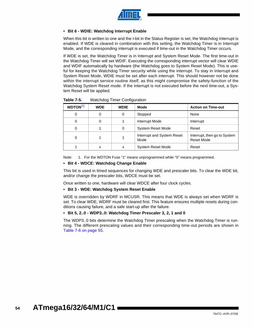
• Bit 6 - WDIE: Watchdog Interrupt Enable
When this bit is written to one and the I-bit in the Status Register is set, the Watchdog Interrupt isenabled. If WDE is cleared in combination with this setting, the Watchdog Timer is in InterruptMode, and the corresponding interrupt is executed if time-out in the Watchdog Timer occurs.
If WDE is set, the Watchdog Timer is in Interrupt and System Reset Mode. The first time-out inthe Watchdog Timer will set WDIF. Executing the corresponding interrupt vector will clear WDIEand WDIF automatically by hardware (the Watchdog goes to System Reset Mode). This is use-ful for keeping the Watchdog Timer security while using the interrupt. To stay in Interrupt andSystem Reset Mode, WDIE must be set after each interrupt. This should however not be donewithin the interrupt service routine itself, as this might compromise the safety-function of theWatchdog System Reset mode. If the interrupt is not executed before the next time-out, a Sys-tem Reset will be applied.
Note: 1. For the WDTON Fuse “1” means unprogrammed while “0” means programmed.• Bit 4 - WDCE: Watchdog Change Enable
This bit is used in timed sequences for changing WDE and prescaler bits. To clear the WDE bit,and/or change the prescaler bits, WDCE must be set.
Once written to one, hardware will clear WDCE after four clock cycles.• Bit 3 - WDE: Watchdog System Reset Enable
WDE is overridden by WDRF in MCUSR. This means that WDE is always set when WDRF isset. To clear WDE, WDRF must be cleared first. This feature ensures multiple resets during con-ditions causing failure, and a safe start-up after the failure.• Bit 5, 2..0 - WDP3..0: Watchdog Timer Prescaler 3, 2, 1 and 0
The WDP3..0 bits determine the Watchdog Timer prescaling when the Watchdog Timer is run-ning. The different prescaling values and their corresponding time-out periods are shown inTable 7-6 on page 55.
Table 7-5. Watchdog Timer Configuration
WDTON(1) WDE WDIE Mode Action on Time-out
0 0 0 Stopped None
0 0 1 Interrupt Mode Interrupt
0 1 0 System Reset Mode Reset
0 1 1 Interrupt and System Reset Mode
Interrupt, then go to System Reset Mode
1 x x System Reset Mode Reset
547647C–AVR–07/08
ATmega16/32/64/M1/C1

ATmega16/32/64/M1/C1
.
Table 7-6. Watchdog Timer Prescale Select
WDP3 WDP2 WDP1 WDP0Number of WDT Oscillator
CyclesTypical Time-out at
VCC = 5.0V
0 0 0 0 2K (2048) cycles 16 ms
0 0 0 1 4K (4096) cycles 32 ms
0 0 1 0 8K (8192) cycles 64 ms
0 0 1 1 16K (16384) cycles 0.125 s
0 1 0 0 32K (32768) cycles 0.25 s
0 1 0 1 64K (65536) cycles 0.5 s
0 1 1 0 128K (131072) cycles 1.0 s
0 1 1 1 256K (262144) cycles 2.0 s
1 0 0 0 512K (524288) cycles 4.0 s
1 0 0 1 1024K (1048576) cycles 8.0 s
1 0 1 0
Reserved
1 0 1 1
1 1 0 0
1 1 0 1
1 1 1 0
1 1 1 1
557647C–AVR–07/08

8. InterruptsThis sect ion descr ibes the spec i f ics o f the in terrupt handl ing as per formed inATmega16/32/64/M1/C1. For a general explanation of the AVR interrupt handling, refer to“Reset and Interrupt Handling” on page 17.
8.1 Interrupt Vectors in ATmega16/32/64/M1/C1
Table 8-1. Reset and Interrupt Vectors
VectorNo.
ProgramAddress Source Interrupt Definition
1 0x0000 RESET External Pin, Power-on Reset, Brown-out Reset, Watchdog Reset, and Emulation AVR Reset
2 0x0002 ANACOMP 0 Analog Comparator 0
3 0x0004 ANACOMP 1 Analog Comparator 1
4 0x0006 ANACOMP 2 Analog Comparator 2
5 0x0008 ANACOMP 3 Analog Comparator 3
6 0x000A PSC FAULT(3) PSC Fault
7 0x000C PSC EC(3) PSC End of Cycle
8 0x000E INT0 External Interrupt Request 0
9 0x0010 INT1 External Interrupt Request 1
10 0x0012 INT2 External Interrupt Request 2
11 0x0014 INT3 External Interrupt Request 3
12 0x0016 TIMER1 CAPT Timer/Counter1 Capture Event
13 0x0018 TIMER1 COMPA Timer/Counter1 Compare Match A
14 0x001A TIMER1 COMPB Timer/Counter1 Compare Match B
15 0x001C TIMER1 OVF Timer/Counter1 Overflow
16 0x001E TIMER0 COMPA Timer/Counter0 Compare Match A
17 0x0020 TIMER0 COMPB Timer/Counter0 Compare Match B
18 0x0022 TIMER0 OVF Timer/Counter0 Overflow
19 0x0024 CAN INT CAN MOB, Burst, General Errors
20 0x0026 CAN TOVF CAN Timer Overflow
21 0x0028 LIN TC LIN Transfer Complete
22 0x002A LIN ERR LIN Error
23 0x002C PCINT0 Pin Change Interrupt Request 0
24 0x002E PCINT1 Pin Change Interrupt Request 1
25 0x0030 PCINT2 Pin Change Interrupt Request 2
26 0x0032 PCINT3 Pin Change Interrupt Request 3
27 0x0034 SPI, STC SPI Serial Transfer Complete
28 0x0036 ADC ADC Conversion Complete
567647C–AVR–07/08
ATmega16/32/64/M1/C1

ATmega16/32/64/M1/C1
Notes: 1. When the BOOTRST Fuse is programmed, the device will jump to the Boot Loader address atreset, see “Boot Loader Support – Read-While-Write Self-ProgrammingATmega16/32/64/M1/C1” on page 275.
2. When the IVSEL bit in MCUCR is set, Interrupt Vectors will be moved to the start of the BootFlash Section. The address of each Interrupt Vector will then be the address in this tableadded to the start address of the Boot Flash Section.
3. These vectors are not used by ATmega32/64C1.
Table 8-2 shows reset and Interrupt Vectors placement for the various combinations ofBOOTRST and IVSEL settings. If the program never enables an interrupt source, the InterruptVectors are not used, and regular program code can be placed at these locations. This is alsothe case if the Reset Vector is in the Application section while the Interrupt Vectors are in theBoot section or vice versa.
Note: 1. The Boot Reset Address is shown in Table 24-4 on page 280. For the BOOTRST Fuse “1” means unprogrammed while “0” means programmed.
The most typical and general program setup for the Reset and Interrupt Vector Addresses inATmega16/32/64/M1/C1 is:
Address Labels Code Comments
0x000 jmp RESET ; Reset Handler
0x002 jmp ANA_COMP_0 ; Analog Comparator 0 Handler
0x004 jmp ANA_COMP_1 ; Analog Comparator 1 Handler
0x006 jmp ANA_COMP_2 ; Analog Comparator 2 Handler
0x008 jmp ANA_COMP_3 ; Analog Comparator 3 Handler
0x00A jmp PSC_FAULT ; PSC Fault Handler
0x00C jmp PSC_EC ; PSC End of Cycle Handler
0x00E jmp EXT_INT0 ; IRQ0 Handler
0x010 jmp EXT_INT1 ; IRQ1 Handler
0x012 jmp EXT_INT2 ; IRQ2 Handler
0x014 jmp EXT_INT3 ; IRQ3 Handler
0x016 jmp TIM1_CAPT ; Timer1 Capture Handler
0x018 jmp TIM1_COMPA ; Timer1 Compare A Handler
0x01A jmp TIM1_COMPB ; Timer1 Compare B Handler
0x01C jmp TIM1_OVF ; Timer1 Overflow Handler
29 0x0038 WDT Watchdog Time-Out Interrupt
30 0x003A EE READY EEPROM Ready
31 0x003C SPM READY Store Program Memory Ready
Table 8-2. Reset and Interrupt Vectors Placement in ATmega16/32/64/M1/C1(1)
BOOTRST IVSEL Reset Address Interrupt Vectors Start Address
1 0 0x000 0x001
1 1 0x000 Boot Reset Address + 0x002
0 0 Boot Reset Address 0x001
0 1 Boot Reset Address Boot Reset Address + 0x002
Table 8-1. Reset and Interrupt Vectors
VectorNo.
ProgramAddress Source Interrupt Definition
577647C–AVR–07/08

0x01E jmp TIM0_COMPA ; Timer0 Compare A Handler
0x020 jmp TIM0_COMPB ; Timer0 Compare B Handler
0x022 jmp TIM0_OVF ; Timer0 Overflow Handler
0x024 jmp CAN_INT ; CAN MOB,Burst,General Errors Handler
0x026 jmp CAN_TOVF ; CAN Timer Overflow Handler
0x028 jmp LIN_TC ; LIN Transfer Complete Handler
0x02A jmp LIN_ERR ; LIN Error Handler
0x02C jmp PCINT0 ; Pin Change Int Request 0 Handler
0x02E jmp PCINT1 ; Pin Change Int Request 1 Handler
0x030 jmp PCINT2 ; Pin Change Int Request 2 Handler
0x032 jmp PCINT3 ; Pin Change Int Request 3 Handler
0x034 jmp SPI_STC ; SPI Transfer Complete Handler
0x036 jmp ADC ; ADC Conversion Complete Handler
0x038 jmp WDT ; Watchdog Timer Handler
0x03A jmp EE_RDY ; EEPROM Ready Handler
0x03C jmp SPM_RDY ; Store Program Memory Ready Handler
;
0x03ERESET: ldi r16, high(RAMEND); Main program start
0x03F out SPH,r16 ; Set Stack Pointer to top of RAM
0x040 ldi r16, low(RAMEND)
0x041 out SPL,r160x042 sei ; Enable interrupts
0x043 <instr> xxx
... ... ... ...
When the BOOTRST Fuse is unprogrammed, the Boot section size set to 2K bytes and theIVSEL bit in the MCUCR Register is set before any interrupts are enabled, the most typical andgeneral program setup for the Reset and Interrupt Vector Addresses in ATmega16/32/64/M1/C1is:
Address Labels Code Comments
0x000 RESET: ldi r16,high(RAMEND); Main program start
0x001 out SPH,r16 ; Set Stack Pointer to top of RAM
0x002 ldi r16,low(RAMEND)
0x003 out SPL,r160x004 sei ; Enable interrupts
0x005 <instr> xxx
;
.org 0xC02
0xC02 jmp ANA_COMP_0 ; Analog Comparator 0 Handler
0xC04 jmp ANA_COMP_1 ; Analog Comparator 1 Handler
... ... ... ;
0xC3C jmp SPM_RDY ; Store Program Memory Ready Handler
When the BOOTRST Fuse is programmed and the Boot section size set to 2K bytes, the mosttypical and general program setup for the Reset and Interrupt Vector Addresses inATmega16/32/64/M1/C1 is:
Address Labels Code Comments
.org 0x002
0x002 jmp ANA_COMP_0 ; Analog Comparator 0 Handler
587647C–AVR–07/08
ATmega16/32/64/M1/C1

ATmega16/32/64/M1/C1
0x004 jmp ANA_COMP_1 ; Analog Comparator 1 Handler
... ... ... ;
0x03C jmp SPM_RDY ; Store Program Memory Ready Handler
;
.org 0xC000xC00 RESET: ldi r16,high(RAMEND); Main program start
0xC01 out SPH,r16 ; Set Stack Pointer to top of RAM
0xC02 ldi r16,low(RAMEND)
0xC03 out SPL,r160xC04 sei ; Enable interrupts
0xC05 <instr> xxx
When the BOOTRST Fuse is programmed, the Boot section size set to 2K bytes and the IVSELbit in the MCUCR Register is set before any interrupts are enabled, the most typical and generalprogram setup for the Reset and Interrupt Vector Addresses in ATmega16/32/64/M1/C116/32 is:
Address Labels Code Comments
;
.org 0xC000xC00 jmp RESET ; Reset handler
0xC02 jmp ANA_COMP_0 ; Analog Comparator 0 Handler
0xC04 jmp ANA_COMP_1 ; Analog Comparator 1 Handler
... ... ... ;
0xC3C jmp SPM_RDY ; Store Program Memory Ready Handler
;
0xC3E RESET: ldi r16,high(RAMEND); Main program start
0xC3F out SPH,r16 ; Set Stack Pointer to top of RAM
0xC40 ldi r16,low(RAMEND)
0xC41 out SPL,r160xC42 sei ; Enable interrupts
0xC43 <instr> xxx
8.1.1 Moving Interrupts Between Application and Boot Space
The MCU Control Register controls the placement of the Interrupt Vector table.
8.1.2 MCU Control Register – MCUCR
• Bit 1 – IVSEL: Interrupt Vector Select
When the IVSEL bit is cleared (zero), the Interrupt Vectors are placed at the start of the Flashmemory. When this bit is set (one), the Interrupt Vectors are moved to the beginning of the BootLoader section of the Flash. The actual address of the start of the Boot Flash Section is deter-mined by the BOOTSZ Fuses. Refer to the section “Boot Loader Support – Read-While-WriteSelf-Programming ATmega16/32/64/M1/C1” on page 275 for details. To avoid unintentional
Bit 7 6 5 4 3 2 1 0
SPIPS – – PUD – – IVSEL IVCE MCUCRRead/Write R/W R R R/W R R R/W R/W
Initial Value 0 0 0 0 0 0 0 0
597647C–AVR–07/08

changes of Interrupt Vector tables, a special write procedure must be followed to change theIVSEL bit:
1. Write the Interrupt Vector Change Enable (IVCE) bit to one.2. Within four cycles, write the desired value to IVSEL while writing a zero to IVCE.
Interrupts will automatically be disabled while this sequence is executed. Interrupts are disabledin the cycle IVCE is set, and they remain disabled until after the instruction following the write toIVSEL. If IVSEL is not written, interrupts remain disabled for four cycles. The I-bit in the StatusRegister is unaffected by the automatic disabling.Note: If Interrupt Vectors are placed in the Boot Loader section and Boot Lock bit BLB02 is pro-
grammed, interrupts are disabled while executing from the Application section. If Interrupt Vectorsare placed in the Application section and Boot Lock bit BLB12 is programed, interrupts are dis-abled while executing from the Boot Loader section. Refer to the section “Boot Loader Support –Read-While-Write Self-Programming ATmega16/32/64/M1/C1” on page 275 for details on BootLock bits.
• Bit 0 – IVCE: Interrupt Vector Change Enable
The IVCE bit must be written to logic one to enable change of the IVSEL bit. IVCE is cleared byhardware four cycles after it is written or when IVSEL is written. Setting the IVCE bit will disableinterrupts, as explained in the IVSEL description above. See Code Example below.
Assembly Code Example
Move_interrupts:
; Enable change of Interrupt Vectors
ldi r16, (1<<IVCE)
out MCUCR, r16
; Move interrupts to Boot Flash section
ldi r16, (1<<IVSEL)
out MCUCR, r16
ret
C Code Example
void Move_interrupts(void)
{
/* Enable change of Interrupt Vectors */
MCUCR = (1<<IVCE);
/* Move interrupts to Boot Flash section */
MCUCR = (1<<IVSEL);
}
607647C–AVR–07/08
ATmega16/32/64/M1/C1

ATmega16/32/64/M1/C1
9. I/O-Ports
9.1 IntroductionAll AVR ports have true Read-Modify-Write functionality when used as general digital I/O ports.This means that the direction of one port pin can be changed without unintentionally changingthe direction of any other pin with the SBI and CBI instructions. The same applies when chang-ing drive value (if configured as output) or enabling/disabling of pull-up resistors (if configured asinput). Each output buffer has symmetrical drive characteristics with both high sink and sourcecapability. All port pins have individually selectable pull-up resistors with a supply-voltage invari-ant resistance. All I/O pins have protection diodes to both VCC and Ground as indicated in Figure9-1. Refer to “Electrical Characteristics” on page 314 for a complete list of parameters.
Figure 9-1. I/O Pin Equivalent Schematic
All registers and bit references in this section are written in general form. A lower case “x” repre-sents the numbering letter for the port, and a lower case “n” represents the bit number. However,when using the register or bit defines in a program, the precise form must be used. For example,PORTB3 for bit no. 3 in Port B, here documented generally as PORTxn. The physical I/O Regis-ters and bit locations are listed in “Register Description for I/O-Ports”.
Three I/O memory address locations are allocated for each port, one each for the Data Register– PORTx, Data Direction Register – DDRx, and the Port Input Pins – PINx. The Port Input PinsI/O location is read only, while the Data Register and the Data Direction Register are read/write.However, writing a logic one to a bit in the PINx Register, will result in a toggle in the correspond-ing bit in the Data Register. In addition, the Pull-up Disable – PUD bit in MCUCR disables thepull-up function for all pins in all ports when set.
Using the I/O port as General Digital I/O is described in “Ports as General Digital I/O”. Most portpins are multiplexed with alternate functions for the peripheral features on the device. How eachalternate function interferes with the port pin is described in “Alternate Port Functions” on page66. Refer to the individual module sections for a full description of the alternate functions.
Note that enabling the alternate function of some of the port pins does not affect the use of theother pins in the port as general digital I/O.
Cpin
Logic
Rpu
See Figure"General Digital I/O" for
Details
Pxn
617647C–AVR–07/08

9.2 Ports as General Digital I/OThe ports are bi-directional I/O ports with optional internal pull-ups. Figure 9-2 shows a func-tional description of one I/O-port pin, here generically called Pxn.
Figure 9-2. General Digital I/O(1)
Note: 1. WRx, WPx, WDx, RRx, RPx, and RDx are common to all pins within the same port. clkI/O,SLEEP, and PUD are common to all ports.
9.2.1 Configuring the Pin
Each port pin consists of three register bits: DDxn, PORTxn, and PINxn. As shown in “RegisterDescription for I/O-Ports” on page 80, the DDxn bits are accessed at the DDRx I/O address, thePORTxn bits at the PORTx I/O address, and the PINxn bits at the PINx I/O address.
The DDxn bit in the DDRx Register selects the direction of this pin. If DDxn is written logic one,Pxn is configured as an output pin. If DDxn is written logic zero, Pxn is configured as an inputpin.
If PORTxn is written logic one when the pin is configured as an input pin, the pull-up resistor isactivated. To switch the pull-up resistor off, PORTxn has to be written logic zero or the pin has tobe configured as an output pin
The port pins are tri-stated when reset condition becomes active, even if no clocks are running.
clk
RPx
RRx
RDx
WDx
PUD
SYNCHRONIZER
WDx: WRITE DDRx
WRx: WRITE PORTxRRx: READ PORTx REGISTERRPx: READ PORTx PIN
PUD: PULLUP DISABLE
clkI/O: I/O CLOCK
RDx: READ DDRx
D
L
Q
Q
RESET
RESET
Q
QD
Q
Q D
CLR
PORTxn
Q
Q D
CLR
DDxn
PINxn
DAT
A B
US
SLEEP
SLEEP: SLEEP CONTROL
Pxn
I/O
WPx
0
1
WRx
WPx: WRITE PINx REGISTER
627647C–AVR–07/08
ATmega16/32/64/M1/C1

ATmega16/32/64/M1/C1
If PORTxn is written logic one when the pin is configured as an output pin, the port pin is drivenhigh (one). If PORTxn is written logic zero when the pin is configured as an output pin, the portpin is driven low (zero).
9.2.2 Toggling the Pin
Writing a logic one to PINxn toggles the value of PORTxn, independent on the value of DDRxn.Note that the SBI instruction can be used to toggle one single bit in a port.
9.2.3 Switching Between Input and Output
When switching between tri-state ({DDxn, PORTxn} = 0b00) and output high ({DDxn, PORTxn}= 0b11), an intermediate state with either pull-up enabled {DDxn, PORTxn} = 0b01) or outputlow ({DDxn, PORTxn} = 0b10) must occur. Normally, the pull-up enabled state is fully accept-able, as a high-impedant environment will not notice the difference between a strong high driverand a pull-up. If this is not the case, the PUD bit in the MCUCR Register can be set to disable allpull-ups in all ports.
Switching between input with pull-up and output low generates the same problem. The usermust use either the tri-state ({DDxn, PORTxn} = 0b00) or the output high state ({DDxn, PORTxn}= 0b11) as an intermediate step.
Table 9-1 summarizes the control signals for the pin value.
9.2.4 Reading the Pin Value
Independent of the setting of Data Direction bit DDxn, the port pin can be read through thePINxn Register bit. As shown in Figure 9-2, the PINxn Register bit and the preceding latch con-stitute a synchronizer. This is needed to avoid metastability if the physical pin changes valuenear the edge of the internal clock, but it also introduces a delay. Figure 9-3 shows a timing dia-gram of the synchronization when reading an externally applied pin value. The maximum andminimum propagation delays are denoted tpd,max and tpd,min respectively.
Table 9-1. Port Pin Configurations
DDxn PORTxnPUD
(in MCUCR) I/O Pull-up Comment
0 0 X Input NoDefault configuration after Reset.Tri-state (Hi-Z)
0 1 0 Input Yes Pxn will source current if ext. pulled low.
0 1 1 Input No Tri-state (Hi-Z)
1 0 X Output No Output Low (Sink)
1 1 X Output No Output High (Source)
637647C–AVR–07/08

Figure 9-3. Synchronization when Reading an Externally Applied Pin value
Consider the clock period starting shortly after the first falling edge of the system clock. The latchis closed when the clock is low, and goes transparent when the clock is high, as indicated by theshaded region of the “SYNC LATCH” signal. The signal value is latched when the system clockgoes low. It is clocked into the PINxn Register at the succeeding positive clock edge. As indi-cated by the two arrows tpd,max and tpd,min, a single signal transition on the pin will be delayedbetween ½ and 1½ system clock period depending upon the time of assertion.
When reading back a software assigned pin value, a nop instruction must be inserted as indi-cated in Figure 9-4. The out instruction sets the “SYNC LATCH” signal at the positive edge ofthe clock. In this case, the delay tpd through the synchronizer is 1 system clock period.
Figure 9-4. Synchronization when Reading a Software Assigned Pin Value
The following code example shows how to set port B pins 0 and 1 high, 2 and 3 low, and definethe port pins from 4 to 7 as input with pull-ups assigned to port pins 6 and 7. The resulting pin
XXX in r17, PINx
0x00 0xFF
INSTRUCTIONS
SYNC LATCH
PINxn
r17
XXX
SYSTEM CLK
tpd, max
tpd, min
out PORTx, r16 nop in r17, PINx
0xFF
0x00 0xFF
SYSTEM CLK
r16
INSTRUCTIONS
SYNC LATCH
PINxn
r17tpd
647647C–AVR–07/08
ATmega16/32/64/M1/C1

ATmega16/32/64/M1/C1
values are read back again, but as previously discussed, a nop instruction is included to be ableto read back the value recently assigned to some of the pins.
Note: 1. For the assembly program, two temporary registers are used to minimize the time from pull-ups are set on pins 0, 1, 6, and 7, until the direction bits are correctly set, defining bit 2 and 3as low and redefining bits 0 and 1 as strong high drivers.
9.2.5 Digital Input Enable and Sleep Modes
As shown in Figure 9-2, the digital input signal can be clamped to ground at the input of theschmitt-trigger. The signal denoted SLEEP in the figure, is set by the MCU Sleep Controller inPower-down mode, Power-save mode, and Standby mode to avoid high power consumption ifsome input signals are left floating, or have an analog signal level close to VCC/2.
SLEEP is overridden for port pins enabled as external interrupt pins. If the external interruptrequest is not enabled, SLEEP is active also for these pins. SLEEP is also overridden by variousother alternate functions as described in “Alternate Port Functions” on page 66.
If a logic high level (“one”) is present on an Asynchronous External Interrupt pin configured as“Interrupt on Rising Edge, Falling Edge, or Any Logic Change on Pin” while the external interruptis not enabled, the corresponding External Interrupt Flag will be set when resuming from theabove mentioned sleep modes, as the clamping in these sleep modes produces the requestedlogic change.
Assembly Code Example(1)
...
; Define pull-ups and set outputs high
; Define directions for port pins
ldi r16, (1<<PB7)|(1<<PB6)|(1<<PB1)|(1<<PB0)
ldi r17, (1<<DDB3)|(1<<DDB2)|(1<<DDB1)|(1<<DDB0)
out PORTB, r16
out DDRB, r17
; Insert nop for synchronization
nop
; Read port pins
in r16, PINB
...
C Code Example
unsigned char i;
...
/* Define pull-ups and set outputs high */
/* Define directions for port pins */
PORTB = (1<<PB7)|(1<<PB6)|(1<<PB1)|(1<<PB0);
DDRB = (1<<DDB3)|(1<<DDB2)|(1<<DDB1)|(1<<DDB0);
/* Insert nop for synchronization*/
_NOP();
/* Read port pins */
i = PINB;
...
657647C–AVR–07/08

9.3 Alternate Port FunctionsMost port pins have alternate functions in addition to being general digital I/Os. Figure 9-5 showshow the port pin control signals from the simplified Figure 9-2 can be overridden by alternatefunctions. The overriding signals may not be present in all port pins, but the figure serves as ageneric description applicable to all port pins in the AVR microcontroller family.
Figure 9-5. Alternate Port Functions(1)
Note: 1. WRx, WPx, WDx, RRx, RPx, and RDx are common to all pins within the same port. clkI/O,SLEEP, and PUD are common to all ports. All other signals are unique for each pin.
Table 9-2 summarizes the function of the overriding signals. The pin and port indexes from Fig-ure 9-5 are not shown in the succeeding tables. The overriding signals are generated internallyin the modules having the alternate function.
clk
RPx
RRxWRx
RDx
WDx
PUD
SYNCHRONIZER
WDx: WRITE DDRx
WRx: WRITE PORTxRRx: READ PORTx REGISTER
RPx: READ PORTx PIN
PUD: PULLUP DISABLE
clkI/O: I/O CLOCK
RDx: READ DDRx
D
L
Q
Q
SET
CLR
0
1
0
1
0
1
DIxn
AIOxn
DIEOExn
PVOVxn
PVOExn
DDOVxn
DDOExn
PUOExn
PUOVxn
PUOExn: Pxn PULL-UP OVERRIDE ENABLE
PUOVxn: Pxn PULL-UP OVERRIDE VALUEDDOExn: Pxn DATA DIRECTION OVERRIDE ENABLE
DDOVxn: Pxn DATA DIRECTION OVERRIDE VALUEPVOExn: Pxn PORT VALUE OVERRIDE ENABLEPVOVxn: Pxn PORT VALUE OVERRIDE VALUE
DIxn: DIGITAL INPUT PIN n ON PORTxAIOxn: ANALOG INPUT/OUTPUT PIN n ON PORTx
RESET
RESET
Q
Q D
CLR
Q
Q D
CLR
Q
QD
CLR
PINxn
PORTxn
DDxn
DAT
A B
US
0
1DIEOVxn
SLEEP
DIEOExn: Pxn DIGITAL INPUT-ENABLE OVERRIDE ENABLE
DIEOVxn: Pxn DIGITAL INPUT-ENABLE OVERRIDE VALUESLEEP: SLEEP CONTROL
Pxn
I/O
0
1
PTOExn
WPx
PTOExn: Pxn, PORT TOGGLE OVERRIDE ENABLE
WPx: WRITE PINx
667647C–AVR–07/08
ATmega16/32/64/M1/C1

ATmega16/32/64/M1/C1
The following subsections shortly describe the alternate functions for each port, and relate theoverriding signals to the alternate function. Refer to the alternate function description for furtherdetails.
Table 9-2. Generic Description of Overriding Signals for Alternate Functions
Signal Name Full Name Description
PUOE Pull-up Override Enable
If this signal is set, the pull-up enable is controlled by the PUOV signal. If this signal is cleared, the pull-up is enabled when {DDxn, PORTxn, PUD} = 0b010.
PUOV Pull-up Override Value
If PUOE is set, the pull-up is enabled/disabled when PUOV is set/cleared, regardless of the setting of the DDxn, PORTxn, and PUD Register bits.
DDOE Data Direction Override Enable
If this signal is set, the Output Driver Enable is controlled by the DDOV signal. If this signal is cleared, the Output driver is enabled by the DDxn Register bit.
DDOV Data Direction Override Value
If DDOE is set, the Output Driver is enabled/disabled when DDOV is set/cleared, regardless of the setting of the DDxn Register bit.
PVOE Port Value Override Enable
If this signal is set and the Output Driver is enabled, the port value is controlled by the PVOV signal. If PVOE is cleared, and the Output Driver is enabled, the port Value is controlled by the PORTxn Register bit.
PVOV Port Value Override Value
If PVOE is set, the port value is set to PVOV, regardless of the setting of the PORTxn Register bit.
PTOE Port Toggle Override Enable If PTOE is set, the PORTxn Register bit is inverted.
DIEOEDigital Input Enable Override Enable
If this bit is set, the Digital Input Enable is controlled by the DIEOV signal. If this signal is cleared, the Digital Input Enable is determined by MCU state (Normal mode, sleep mode).
DIEOVDigital Input Enable Override Value
If DIEOE is set, the Digital Input is enabled/disabled when DIEOV is set/cleared, regardless of the MCU state (Normal mode, sleep mode).
DI Digital Input
This is the Digital Input to alternate functions. In the figure, the signal is connected to the output of the schmitt trigger but before the synchronizer. Unless the Digital Input is used as a clock source, the module with the alternate function will use its own synchronizer.
AIO Analog Input/Output
This is the Analog Input/output to/from alternate functions. The signal is connected directly to the pad, and can be used bi-directionally.
677647C–AVR–07/08

9.3.1 MCU Control Register – MCUCR
• Bit 4 – PUD: Pull-up Disable
When this bit is written to one, the pull-ups in the I/O ports are disabled even if the DDxn andPORTxn Registers are configured to enable the pull-ups ({DDxn, PORTxn} = 0b01). Se
9.3.2 Alternate Functions of Port B
The Port B pins with alternate functions are shown in Table 9-3.
The alternate pin configuration is as follows:• ADC4/PSCOUT0B/SCK/PCINT7 – Bit 7
PSCOUT0B, Output 0B of PSC.
Bit 7 6 5 4 3 2 1 0
SPIPS – – PUD – – IVSEL IVCE MCUCRRead/Write R/W R R R/W R R R/W R/W
Initial Value 0 0 0 0 0 0 0 0
Table 9-3. Port B Pins Alternate Functions
Port Pin Alternate Functions
PB7
PSCOUT0B (PSC output 0B)ADC4 (Analog Input Channel 4)SCK (SPI Bus Serial Clock)PCINT7 (Pin Change Interrupt 7)
PB6ADC7 (Analog Input Channel 7)PSCOUT1B (PSC output 1B)PCINT6 (Pin Change Interrupt 6)
PB5
ADC6 (Analog Input Channel 6)INT2 (External Interrupt 2)ACMPN1 (Analog Comparator 1 Negative Input)AMP2- (Analog Differential Amplicator 2 Negative Input)PCINT5 (Pin Change Interrupt 5)
PB4AMP0+ (Analog Differential Amplifier 0 Positive Input)PCINT4 (Pin Change Interrupt 4)
PB3AMP0- (Analog Differential Amplifier 0 Negative Input)PCINT3 (Pin Change Interrupt 3)
PB2
ADC5 (Analog Input Channel5 )INT1 (External Interrupt 1)ACMPN0 (Analog Comparator 0 Negative Input)PCINT2 (Pin Change Interrupt 2)
PB1MOSI (SPI Master Out Slave In)PSCOUT2B (PSC output 2B)PCINT1 (Pin Change Interrupt 1)
PB0MISO (SPI Master In Slave Out)PSCOUT2A (PSC output 2A)PCINT0 (Pin Change Interrupt 0)
687647C–AVR–07/08
ATmega16/32/64/M1/C1

ATmega16/32/64/M1/C1
ADC4, Analog to Digital Converter, input channel 4.
SCK, Master Clock output, Slave Clock input pin for SPI channel. When the SPI is enabled as aslave, this pin is configured as an input regardless of the setting of DDB7. When the SPI isenabled as a master, the data direction of this pin is controlled by DDB7. When the pin is forcedto be an input, the pull-up can still be controlled by the PORTB7 bit.
PCINT7, Pin Change Interrupt 7.• ADC7/PSCOUT1B/PCINT6 – Bit 6
ADC7, Analog to Digital Converter, input channel 7.
PSCOUT1B, Output 1B of PSC.
PCINT6, Pin Change Interrupt 6.• ADC6/INT2/ACMPN1/AMP2-/PCINT5 – Bit 5
ADC6, Analog to Digital Converter, input channel 6.
INT2, External Interrupt source 2. This pin can serve as an External Interrupt source to the MCU.
ACMPN1, Analog Comparator 1 Negative Input. Configure the port pin as input with the internalpull-up switched off to avoid the digital port function from interfering with the function of the Ana-log Comparator.
PCINT5, Pin Change Interrupt 5.• APM0+/PCINT4 – Bit 4
AMP0+, Analog Differential Amplifier 0 Positive Input Channel.
PCINT4, Pin Change Interrupt 4.• AMP0-/PCINT3 – Bit 3
AMP0-, Analog Differential Amplifier 0 Negative Input Channel. Configure the port pin as inputwith the internal pull-up switched off to avoid the digital port function from interfering with thefunction of the Analog Amplifier.
PCINT3, Pin Change Interrupt 3.• ADC5/INT1/ACMPN0/PCINT2 – Bit 2
ADC5, Analog to Digital Converter, input channel 5.
INT1, External Interrupt source 1. This pin can serve as an external interrupt source to the MCU.
ACMPN0, Analog Comparator 0 Negative Input. Configure the port pin as input with the internalpull-up switched off to avoid the digital port function from interfering with the function of the Ana-log Comparator.
PCINT2, Pin Change Interrupt 2.• PCINT1/MOSI/PSCOUT2B – Bit 1
MOSI: SPI Master Data output, Slave Data input for SPI channel. When the SPI is enabled as aslave, this pin is configured as an input regardless of the setting of DDB1 When the SPI isenabled as a master, the data direction of this pin is controlled by DDB1. When the pin is forcedto be an input, the pull-up can still be controlled by the PORTB1 and PUD bits.
PSCOUT2B, Output 2B of PSC.
PCINT1, Pin Change Interrupt 1.• PCINT0/MISO/PSCOUT2A – Bit 0
697647C–AVR–07/08

MISO, Master Data input, Slave Data output pin for SPI channel. When the SPI is enabled as amaster, this pin is configured as an input regardless of the setting of DDB0. When the SPI isenabled as a slave, the data direction of this pin is controlled by DDB0. When the pin is forced tobe an input, the pull-up can still be controlled by the PORTB0 and PUD bits.
PSCOUT2A, Output 2A of PSC.
PCINT0, Pin Change Interrupt 0.
Table 9-4 and Table 9-5 relates the alternate functions of Port B to the overriding signals shownin Figure 9-5 on page 66.
Table 9-4. Overriding Signals for Alternate Functions in PB7..PB4
Signal Name
PB7/ADC4/PSCOUT0B/SCK/PCINT7
PB6/ADC7/PSCOUT1B/PCINT6
PB5/ADC6/INT2/ACMPN1/AMP2-/PCINT5
PB4/AMP0+/PCINT4
PUOE SPE • MSTR • SPIPS 0 0 0
PUOV PB7 • PUD • SPIPS 0 0 0
DDOESPE • MSTR • SPIPS+ PSCen01
PSCen11 0 0
DDOV PSCen01 1 0 0
PVOE SPE • MSTR • SPIPS PSCen11 0 0
PVOV
PSCout01 • SPIPS + PSCout01 • PSCen01 • SPIPS+ PSCout01 • PSCen01 • SPIPS
PSCOUT11 0 0
DIEOE ADC4D ADC7D ADC6D + In2en AMP0ND
DIEOV 0 0 In2en 0
DI SCKin • SPIPS • ireset ICP1B INT2
AIO ADC4 ADC7 ADC6 AMP0+
707647C–AVR–07/08
ATmega16/32/64/M1/C1

ATmega16/32/64/M1/C1
Table 9-5. Overriding Signals for Alternate Functions in PB3..PB0
Signal NamePB3/AMP0-/PCINT3
PB2/ADC5/INT1/ACMPN0/PCINT2
PB1/MOSI/PSCOUT2B/PCINT1
PB0/MISO/PSCOUT2A/PCINT0
PUOE 0 0 – –
PUOV 0 0 – –
DDOE 0 0 – –
DDOV 0 0 – –
PVOE 0 0 – –
PVOV 0 0 – –
DIEOE AMP0ND ADC5D + In1en 0 0
DIEOV 0 In1en 0 0
DI INT1 MOSI_IN • SPIPS • ireset
MISO_IN • SPIPS • ireset
AIO AMP0- ADC5 – –
717647C–AVR–07/08

9.3.3 Alternate Functions of Port C
The Port C pins with alternate functions are shown in Table 9-6.
Note: On the engineering samples (Parts marked AT90PWM324), the ACMPN3 alternate function is not located on PC4. It is located on PE2.
The alternate pin configuration is as follows:• D2A/AMP2+/PCINT15 – Bit 7
D2A, Digital to Analog output
AMP2+, Analog Differential Amplifier 2 Positive Input. Configure the port pin as input with theinternal pull-up switched off to avoid the digital port function from interfering with the function ofthe Amplifier.
PCINT15, Pin Change Interrupt 15.• ADC10/ACMP1/PCINT14 – Bit 6
ADC10, Analog to Digital Converter, input channel 10.
Table 9-6. Port C Pins Alternate Functions
Port Pin Alternate Function
PC7D2A (DAC output )AMP2+ (Analog Differential Amplifier 2 Positive Input)PCINT15 (Pin Change Interrupt 15)
PC6ADC10 (Analog Input Channel 10)ACMP1 (Analog Comparator 1 Positive Input )PCINT14 (Pin Change Interrupt 14)
PC5
ADC9 (Analog Input Channel 9)AMP1+ (Analog Differential Amplifier 1 Input Channel )ACMP3 (Analog Comparator 3 Positive Input )PCINT13 (Pin Change Interrupt 13)
PC4
ADC8 (Analog Input Channel 8)AMP1- (Analog Differential Amplifier 1 Input Channel )ACMPN3 (Analog Comparator 3 Negative Input)PCINT12 (Pin Change Interrupt 12)
PC3
T1 (Timer 1 clock input)RXCAN (CAN Rx Data)ICP1B (Timer 1 input capture alternate input)PCINT11 (Pin Change Interrupt 11)
PC2T0 (Timer 0 clock input)TXCAN (CAN Tx Data)PCINT10 (Pin Change Interrupt 10)
PC1
PSCIN1 (PSC 1 Digital Input)OC1B (Timer 1 Output Compare B)SS_A (Alternate SPI Slave Select)PCINT9 (Pin Change Interrupt 9)
PC0PSCOUT1A (PSC output 2A) INT3 (External Interrupt 3)PCINT8 (Pin Change Interrupt 8)
727647C–AVR–07/08
ATmega16/32/64/M1/C1

ATmega16/32/64/M1/C1
ACMP1, Analog Comparator 1 Positive Input. Configure the port pin as input with the internalpull-up switched off to avoid the digital port function from interfering with the function of the Ana-log Comparator.
PCINT14, Pin Change Interrupt 14.• ADC9/ACMP3/AMP1+/PCINT13 – Bit 5
ADC9, Analog to Digital Converter, input channel 9.
ACMP3, Analog Comparator 3 Positive Input. Configure the port pin as input with the internalpull-up switched off to avoid the digital port function from interfering with the function of the Ana-log Comparator.
AMP1+, Analog Differential Amplifier 1 Positive Input Channel. Configure the port pin as inputwith the internal pull-up switched off to avoid the digital port function from interfering with thefunction of the Analog Amplifier.
PCINT13, Pin Change Interrupt 13.• ADC8/AMP1-/ACMPN3/PCINT12 – Bit 4
ADC8, Analog to Digital Converter, input channel 8.
AMP1-, Analog Differential Amplifier 1 Negative Input Channel. Configure the port pin as inputwith the internal pull-up switched off to avoid the digital port function from interfering with thefunction of the Analog Amplifier.
ACMPN3, Analog Comparator 3 Negative Input. Configure the port pin as input with the internalpull-up switched off to avoid the digital port function from interfering with the function of the Ana-log Comparator.
PCINT12, Pin Change Interrupt 12.• PCINT11/T1/RXCAN/ICP1B – Bit 3
T1, Timer/Counter1 counter source.
RXCAN, CAN Rx Data.
ICP1B, Input Capture Pin: The PC3 pin can act as an Input Capture Pin for Timer/Counter1.
PCINT11, Pin Change Interrupt 11.• PCINT10/T0/TXCAN – Bit 2
T0, Timer/Counter0 counter source.
TXCAN, CAN Tx Data.
PCINT10, Pin Change Interrupt 10.• PCINT9/PSCIN1/OC1B/SS_A – Bit 1
PCSIN1, PSC 1 Digital Input.
OC1B, Output Compare Match B output: This pin can serve as an external output for theTimer/Counter1 Output Compare B. The pin has to be configured as an output (DDC1 set “one”)to serve this function. This pin is also the output pin for the PWM mode timer function.
SS_A: Slave Port Select input. When the SPI is enabled as a slave, this pin is configured as aninput regardless of the setting of DDD0. As a slave, the SPI is activated when this pin is drivenlow. When the SPI is enabled as a master, the data direction of this pin is controlled by DDD0.When the pin is forced to be an input, the pull-up can still be controlled by the PORTD0 bit.
PCINT9, Pin Change Interrupt 9.• PCINT8/PSCOUT1A/INT3 – Bit 0
737647C–AVR–07/08

PSCOUT1A, Output 1A of PSC.
INT3, External Interrupt source 3: This pin can serve as an external interrupt source to the MCU.
PCINT8, Pin Change Interrupt 8.
Table 9-7 and Table 9-8 relate the alternate functions of Port C to the overriding signals shownin Figure 9-5 on page 66.
Table 9-7. Overriding Signals for Alternate Functions in PC7..PC4
Signal NamePC7/D2A/AMP2+/PCINT15
PC6/ADC10/ACMP1/PCINT14
PC5/ADC9/AMP1+/ACMP3/PCINT13
PC4/ADC8/AMP1-/ACMPN3/PCINT12
PUOE 0 0 0
PUOV 0 0 0
DDOE DAEN 0 0 0
DDOV 0 0 0 0
PVOE 0 0 0 –
PVOV 0 0 0 –
DIEOE DAEN ADC10D ADC9D ADC8D
DIEOV 0 0 0 0
DI
AIO – ADC10 Amp1 ADC9 Amp1+ADC8 Amp1-ACMPN3
Table 9-8. Overriding Signals for Alternate Functions in PC3..PC0
Signal NamePC3/T1/RXCAN/ICP1B/PCINT11
PC2/T0/TXCAN/PCINT10
PC1/PSCIN1/OC1B/SS_A/PCINT9
PC0/INT3/PSCOUT1A/PCINT8
PUOE 0 0 0 0
PUOV 0 0 0 0
DDOE 0 PSCen10
DDOV 1 1 0 1
PVOE OC1Ben PSCen10
PVOV OC1B PSCout10
DIEOE In3en
DIEOV In3en
DI T1 T0PSCin1SS_A
INT3
AIO
747647C–AVR–07/08
ATmega16/32/64/M1/C1

ATmega16/32/64/M1/C1
9.3.4 Alternate Functions of Port D
The Port D pins with alternate functions are shown in Table 9-9.
The alternate pin configuration is as follows:
• ACMP0/PCINT23 – Bit 7
ACMP0, Analog Comparator 0 Positive Input. Configure the port pin as input with the internalpull-up switched off to avoid the digital port function from interfering with the function of the Ana-log Comparator.
PCINT23, Pin Change Interrupt 23.• ADC3/ACMPN2/INT0/PCINT22 – Bit 6
ADC3, Analog to Digital Converter, input channel 3.
Table 9-9. Port D Pins Alternate Functions
Port Pin Alternate Function
PD7ACMP0 (Analog Comparator 0 Positive Input )PCINT23 (Pin Change Interrupt 23)
PD6
ADC3 (Analog Input Channel 3 )ACMPN2 (Analog Comparator 2 Negative Input)INT0 (External Interrupt 0)PCINT22 (Pin Change Interrupt 22)
PD5ADC2 (Analog Input Channel 2)ACMP2 (Analog Comparator 2 Positive Input )PCINT21 (Pin Change Interrupt 21)
PD4
ADC1 (Analog Input Channel 1)RXD/RXLIN (LIN/UART Rx data)ICP1A (Timer 1 input capture)SCK_A (Programming & alternate SPI Clock)PCINT20 (Pin Change Interrupt 20)
PD3
TXD/TXLIN (LIN/UART Tx data)OC0A (Timer 0 Output Compare A)SS (SPI Slave Select)MOSI_A (Programming & alternate SPI Master Out Slave In)PCINT19 (Pin Change Interrupt 19)
PD2
PSCIN2 (PSC Digital Input 2) OC1A (Timer 1 Output Compare A)MISO_A (Programming & alternate Master In SPI Slave Out)PCINT18 (Pin Change Interrupt 18)
PD1PSCIN0 (PSC Digital Input 0)CLKO (System Clock Output)PCINT17 (Pin Change Interrupt 17)
PD0PSCOUT0A (PSC output 0A)PCINT16 (Pin Change Interrupt 16)
757647C–AVR–07/08

ACMPN2, Analog Comparator 2 Negative Input. Configure the port pin as input with the internalpull-up switched off to avoid the digital port function from interfering with the function of the Ana-log Comparator.
INT0, External Interrupt source 0. This pin can serve as an external interrupt source to the MCU.
PCINT22, Pin Change Interrupt 23.• ADC2/ACMP2/PCINT21 – Bit 5
ADC2, Analog to Digital Converter, input channel 2.
ACMP2, Analog Comparator 1 Positive Input. Configure the port pin as input with the internalpull-up switched off to avoid the digital port function from interfering with the function of the Ana-log Comparator.
PCINT21, Pin Change Interrupt 21.• PCINT20/ADC1/RXD/RXLIN/ICP1/SCK_A – Bit 4
ADC1, Analog to Digital Converter, input channel 1.
RXD/RXLIN, LIN/UART Receive Pin. Receive Data (Data input pin for the LIN/UART). When theLIN/UART receiver is enabled this pin is configured as an input regardless of the value ofDDRD4. When the UART forces this pin to be an input, a logical one in PORTD4 will turn on theinternal pull-up.
ICP1, Input Capture Pin1: This pin can act as an input capture pin for Timer/Counter1.
SCK_A: Master Clock output, Slave Clock input pin for SPI channel. When the SPI is enabled asa slave, this pin is configured as an input regardless of the setting of DDD4. When the SPI isenabled as a master, the data direction of this pin is controlled by DDD4. When the pin is forcedto be an input, the pull-up can still be controlled by the PORTD4 bit.
PCINT20, Pin Change Interrupt 20.• PCINT19/TXD/TXLIN/OC0A/SS/MOSI_A, Bit 3
TXD/TXLIN, LIN/UART Transmit pin. Data output pin for the LIN/UART. When the LIN/UARTTransmitter is enabled, this pin is configured as an output regardless of the value of DDD3.
OC0A, Output Compare Match A output: This pin can serve as an external output for theTimer/Counter0 Output Compare A. The pin has to be configured as an output (DDD3 set “one”)to serve this function. The OC0A pin is also the output pin for the PWM mode
SS: Slave Port Select input. When the SPI is enabled as a slave, this pin is configured as aninput regardless of the setting of DDD3. As a slave, the SPI is activated when this pin is drivenlow. When the SPI is enabled as a master, the data direction of this pin is controlled by DDD3.When the pin is forced to be an input, the pull-up can still be controlled by the PORTD3 bit.
MOSI_A: SPI Master Data output, Slave Data input for SPI channel. When the SPI is enabled asa slave, this pin is configured as an input regardless of the setting of DDD3 When the SPI isenabled as a master, the data direction of this pin is controlled by DDD3. When the pin is forcedto be an input, the pull-up can still be controlled by the PORTD3 bit.
PCINT19, Pin Change Interrupt 19.• PCINT18/PSCIN2/OC1A/MISO_A, Bit 2
PCSIN2, PSC Digital Input 2.
OC1A, Output Compare Match A output: This pin can serve as an external output for theTimer/Counter1 Output Compare A. The pin has to be configured as an output (DDD2 set “one”)to serve this function. The OC1A pin is also the output pin for the PWM mode timer function.
767647C–AVR–07/08
ATmega16/32/64/M1/C1

ATmega16/32/64/M1/C1
MISO_A: Master Data input, Slave Data output pin for SPI channel. When the SPI is enabled asa master, this pin is configured as an input regardless of the setting of DDD2. When the SPI isenabled as a slave, the data direction of this pin is controlled by DDD2. When the pin is forced tobe an input, the pull-up can still be controlled by the PORTD2 bit.
PCINT18, Pin Change Interrupt 18.• PCINT17/PSCIN0/CLKO – Bit 1
PCSIN0, PSC Digital Input 0.
CLKO, Divided System Clock: The divided system clock can be output on this pin. The dividedsystem clock will be output if the CKOUT Fuse is programmed, regardless of the PORTD1 andDDD1 settings. It will also be output during reset.
PCINT17, Pin Change Interrupt 17.• PCINT16/PSCOUT0A – Bit 0
PSCOUT0A: Output 0 of PSC 0.
PCINT16, Pin Change Interrupt 16.
Table 9-10 and Table 9-11 relates the alternate functions of Port D to the overriding signalsshown in Figure 9-5 on page 66.
Table 9-10. Overriding Signals for Alternate Functions PD7..PD4
Signal Name
PD7/ACMP0/PCINT23
PD6/ADC3/ACMPN2/INT0/PCINT22
PD5/ADC2/ACMP2/PCINT21
PD4/ADC1/RXD/RXLIN/ICP1A/SCK_A/PCINT20
PUOE 0 0 0RXEN + SPE •MSTR • SPIPS
PUOV 0 0 0PD4 •PUD
DDOE 0 0 0RXEN + SPE •MSTR • SPIPS
DDOV 0 0 0 0
PVOE 0 0 0 SPE • MSTR • SPIPS
PVOV 0 0 0 –
DIEOE ACMP0D ADC3D + In0en ADC2D ADC1D
DIEOV 0 In0en 0 0
DI – INT0 ICP1A
AIO ACOMP0ADC3ACMPM
ADC2ACOMP2
ADC1
777647C–AVR–07/08

9.3.5 Alternate Functions of Port E
The Port E pins with alternate functions are shown in Table 9-12.
Note: On the engineering samples (Parts marked AT90PWM324), the ACMPN3 alternate function is not located on PC4. It is located on PE2.
Table 9-11. Overriding Signals for Alternate Functions in PD3..PD0
Signal Name
PD3/TXD/TXLIN/OC0A/SS/MOSI_A/PCINT19
PD2/PSCIN2/OC1A/MISO_A/PCINT18
PD1/PSCIN0/CLKO/PCINT17
PD0/PSCOUT0A/XCK/PCINT16
PUOETXEN + SPE •MSTR • SPIPS
– 0SPE •MSTR • SPIPS
PUOV TXEN • SPE • MSTR • SPIPS • PD3 • PUD – 0 PD0 • PUD
DDOETXEN + SPE •MSTR • SPIPS
– 0PSCen00 + SPE •MSTR • SPIPS
DDOV TXEN 0 0 PSCen00
PVOETXEN + OC0en + SPE •MSTR • SPIPS
– 0 PSCen00 + UMSEL
PVOV
TXEN • TXD + TXEN • (OC0en • OC0 + OC0en • SPIPS • MOSI)
– 0 –
DIEOE 0 0 0 0
DIEOV 0 0 0 0
DISSMOSI_Ain
AIO
Table 9-12. Port E Pins Alternate Functions
Port Pin Alternate Function
PE2XTAL2 (XTAL Output)ADC0 (Analog Input Channel 0)PCINT26 (Pin Change Interrupt 26)
PE1XTAL1 (XTAL Input)OC0B (Timer 0 Output Compare B)PCINT25 (Pin Change Interrupt 25)
PE0RESET# (Reset Input)OCD (On Chip Debug I/O)PCINT24 (Pin Change Interrupt 24)
787647C–AVR–07/08
ATmega16/32/64/M1/C1

ATmega16/32/64/M1/C1
The alternate pin configuration is as follows:• PCINT26/XTAL2/ADC0 – Bit 2
XTAL2: Chip clock Oscillator pin 2. Used as clock pin for crystal Oscillator or Low-frequencycrystal Oscillator. When used as a clock pin, the pin can not be used as an I/O pin.
ADC0, Analog to Digital Converter, input channel 0.
PCINT26, Pin Change Interrupt 26.• PCINT25/XTAL1/OC0B – Bit 1
XTAL1: Chip clock Oscillator pin 1. Used for all chip clock sources except internal calibrated RCOscillator. When used as a clock pin, the pin can not be used as an I/O pin.
OC0B, Output Compare Match B output: This pin can serve as an external output for theTimer/Counter0 Output Compare B. The pin has to be configured as an output (DDE1 set “one”)to serve this function. This pin is also the output pin for the PWM mode timer function.
PCINT25, Pin Change Interrupt 25.• PCINT24/RESET/OCD – Bit 0
RESET, Reset pin: When the RSTDISBL Fuse is programmed, this pin functions as a normal I/Opin, and the part will have to rely on Power-on Reset and Brown-out Reset as its reset sources.When the RSTDISBL Fuse is unprogrammed, the reset circuitry is connected to the pin, and thepin can not be used as an I/O pin.
If PE0 is used as a reset pin, DDE0, PORTE0 and PINE0 will all read 0.
PCINT24, Pin Change Interrupt 24.
Table 9-13 relates the alternate functions of Port E to the overriding signals shown in Figure 9-5on page 66.
Table 9-13. Overriding Signals for Alternate Functions in PE2..PE0
Signal NamePE2/ADC0/XTAL2/PCINT26
PE1/XTAL1/OC0B/PCINT25
PE0/RESET/OCD/PCINT24
PUOE 0 0 0
PUOV 0 0 0
DDOE 0 0 0
DDOV 0 0 0
PVOE 0 OC0Ben 0
PVOV 0 OC0B 0
DIEOE ADC0D 0 0
DIEOV 0 0 0
DI
AIOOsc OutputADC0
Osc / Clock input
797647C–AVR–07/08

9.4 Register Description for I/O-Ports
9.4.1 Port B Data Register – PORTB
9.4.2 Port B Data Direction Register – DDRB
9.4.3 Port B Input Pins Address – PINB
9.4.4 Port C Data Register – PORTC
9.4.5 Port C Data Direction Register – DDRC
9.4.6 Port C Input Pins Address – PINC
9.4.7 Port D Data Register – PORTD
9.4.8 Port D Data Direction Register – DDRD
Bit 7 6 5 4 3 2 1 0
PORTB7 PORTB6 PORTB5 PORTB4 PORTB3 PORTB2 PORTB1 PORTB0 PORTBRead/Write R/W R/W R/W R/W R/W R/W R/W R/W
Initial Value 0 0 0 0 0 0 0 0
Bit 7 6 5 4 3 2 1 0
DDB7 DDB6 DDB5 DDB4 DDB3 DDB2 DDB1 DDB0 DDRBRead/Write R/W R/W R/W R/W R/W R/W R/W R/W
Initial Value 0 0 0 0 0 0 0 0
Bit 7 6 5 4 3 2 1 0
PINB7 PINB6 PINB5 PINB4 PINB3 PINB2 PINB1 PINB0 PINBRead/Write R/W R/W R/W R/W R/W R/W R/W R/W
Initial Value N/A N/A N/A N/A N/A N/A N/A N/A
Bit 7 6 5 4 3 2 1 0
PORTC7 PORTC6 PORTC5 PORTC4 PORTC3 PORTC2 PORTC1 PORTC0 PORTCRead/Write R/W R/W R/W R/W R/W R/W R/W R/W
Initial Value 0 0 0 0 0 0 0 0
Bit 7 6 5 4 3 2 1 0
DDC7 DDC6 DDC5 DDC4 DDC3 DDC2 DDC1 DDC0 DDRCRead/Write R/W R/W R/W R/W R/W R/W R/W R/W
Initial Value 0 0 0 0 0 0 0 0
Bit 7 6 5 4 3 2 1 0
PINC7 PINC6 PINC5 PINC4 PINC3 PINC2 PINC1 PINC0 PINCRead/Write R/W R/W R/W R/W R/W R/W R/W R/W
Initial Value N/A N/A N/A N/A N/A N/A N/A N/A
Bit 7 6 5 4 3 2 1 0
PORTD7 PORTD6 PORTD5 PORTD4 PORTD3 PORTD2 PORTD1 PORTD0 PORTDRead/Write R/W R/W R/W R/W R/W R/W R/W R/W
Initial Value 0 0 0 0 0 0 0 0
Bit 7 6 5 4 3 2 1 0
DDD7 DDD6 DDD5 DDD4 DDD3 DDD2 DDD1 DDD0 DDRDRead/Write R/W R/W R/W R/W R/W R/W R/W R/W
Initial Value 0 0 0 0 0 0 0 0
807647C–AVR–07/08
ATmega16/32/64/M1/C1

ATmega16/32/64/M1/C1
9.4.9 Port D Input Pins Address – PIND
9.4.10 Port E Data Register – PORTE
9.4.11 Port E Data Direction Register – DDRE
9.4.12 Port E Input Pins Address – PINE
Bit 7 6 5 4 3 2 1 0
PIND7 PIND6 PIND5 PIND4 PIND3 PIND2 PIND1 PIND0 PINDRead/Write R/W R/W R/W R/W R/W R/W R/W R/W
Initial Value N/A N/A N/A N/A N/A N/A N/A N/A
Bit 7 6 5 4 3 2 1 0
– – – – – PORTE2 PORTE1 PORTE0 PORTERead/Write R R R R R R/W R/W R/W
Initial Value 0 0 0 0 0 0 0 0
Bit 7 6 5 4 3 2 1 0
– – – – – DDE2 DDE1 DDE0 DDRERead/Write R R R R R R/W R/W R/W
Initial Value 0 0 0 0 0 0 0 0
Bit 7 6 5 4 3 2 1 0
– – – – – PINE2 PINE1 PINE0 PINERead/Write R R R R R R/W R/W R/W
Initial Value 0 0 0 0 0 N/A N/A N/A
817647C–AVR–07/08

10. External InterruptsThe External Interrupts are triggered by the INT3:0 pins or any of the PCINT23..0 pins. Observethat, if enabled, the interrupts will trigger even if the INT3:0 or PCINT23..0 pins are configured asoutputs. This feature provides a way of generating a software interrupt. The pin change interruptPCI2 will trigger if any enabled PCINT23..16 pin toggles. The pin change interrupt PCI1 will trig-ger if any enabled PCINT14..8 pin toggles. The pin change interrupt PCI0 will trigger if anyenabled PCINT7..0 pin toggles. The PCMSK3, PCMSK2, PCMSK1 and PCMSK0 Registerscontrol which pins contribute to the pin change interrupts. Pin change interrupts on PCINT26..0are detected asynchronously. This implies that these interrupts can be used for waking the partalso from sleep modes other than Idle mode.
The INT3:0 interrupts can be triggered by a falling or rising edge or a low level. This is set up asindicated in the specification for the External Interrupt Control Register A – EICRA. When theINT3:0 interrupts are enabled and are configured as level triggered, the interrupts will trigger aslong as the pin is held low. Note that recognition of falling or rising edge interrupts on INT3:0requires the presence of an I/O clock, described in “Clock Systems and their Distribution” onpage 29. Low level interrupt on INT3:0 is detected asynchronously. This implies that this inter-rupt can be used for waking the part also from sleep modes other than Idle mode. The I/O clockis halted in all sleep modes except Idle mode.
Note that if a level triggered interrupt is used for wake-up from Power-down, the required levelmust be held long enough for the MCU to complete the wake-up to trigger the level interrupt. Ifthe level disappears before the end of the Start-up Time, the MCU will still wake up, but no inter-rupt will be generated. The start-up time is defined by the SUT and CKSEL Fuses as describedin “Clock Systems and their Distribution” on page 29.
10.1 Pin Change Interrupt TimingAn example of timing of a pin change interrupt is schown in Figure 10-1.
Figure 10-1. Timing of a pin change interrupts
LE
D Q D Q
clk
pin_lat pin_sync pcint_in[i]PCINT[i]�pin
PCINT[i] bit�(of PCMSKn)
D Q D Q D Q
clk
pcint_sync pcint_set/flag0
7
PCIFn�(interrupt�
flag)
PCINT[i] pin
pin_lat
pin_sync
clk
pcint_in[i]
pcint_syn
pcint_set/flag
PCIFn
827647C–AVR–07/08
ATmega16/32/64/M1/C1

ATmega16/32/64/M1/C1
10.2 External Interrupt Control Register A – EICRAThe External Interrupt Control Register A contains control bits for interrupt sense control.
• Bit 7..0 – ISC31, ISC30 - ISC01, ISC00: Interrupt Sense Control 0 Bit 1 and Bit 0
The External Interrupts 3 - 0 are activated by the external pins INT3:0 if the SREG I-flag and thecorresponding interrupt mask in the EIMSK is set. The level and edges on the external pins thatactivate the interrupt are defined in Table 10-1. Edges on INT3..INT0 are registered asynchro-nously. The value on the INT3:0 pins are sampled before detecting edges. If edge or toggleinterrupt is selected, pulses that last longer than one clock period will generate an interrupt.Shorter pulses are not guaranteed to generate an interrupt. Observe that CPU clock frequencycan be lower than XTAL frequency if the XTAL divider is enabled. If low level interrupt isselected, the low level must be held until the completion of the currently executing instruction togenerate an interrupt. If enabled, a level triggered interrupt will generate an interrupt request aslong as the pin is held low.
Note: 1. n = 3, 2, 1 or 0.When changing the ISCn1/ISCn0 bits, the interrupt must be disabled by clearing its Interrupt Enable bit in the EIMSK Register. Otherwise an interrupt can occur when the bits are changed.
10.2.1 External Interrupt Mask Register – EIMSK
• Bit 7..4 – Res: Reserved Bits
These bits are unused bits in the ATmega16/32/64/M1/C1, and will always read as zero.• Bit 3..0 – INT3 - 0: External Interrupt Request 3:0 Enable
When an INT3 – INT0 bit is written to one and the I-bit in the Status Register (SREG) is set(one), the corresponding external pin interrupt is enabled. The Interrupt Sense Control bits in theExternal Interrupt Control Register A - EICRA defines whether the external interrupt is activatedon rising or falling edge or level sensed. Activity on any of these pins will trigger an interruptrequest even if the pin is enabled as an output. This provides a way of generating a softwareinterrupt.
Bit 7 6 5 4 3 2 1 0
ISC31 ISC30 ISC21 ISC20 ISC11 ISC10 ISC01 ISC00 EICRARead/Write R/W R/W R/W R/W R/W R/W R/W R/W
Initial Value 0 0 0 0 0 0 0 0
Table 10-1. Interrupt Sense Control(1)
ISCn1 ISCn0 Description
0 0 The low level of INTn generates an interrupt request.
0 1 Any logical change on INTn generates an interrupt request.
1 0 The falling edge between two samples of INTn generates an interrupt request.
1 1 The rising edge between two samples of INTn generates an interrupt request.
Bit 7 6 5 4 3 2 1 0
– – – – INT3 INT2 INT1 INT0 EIMSKRead/Write R R R R R R R/W R/W
Initial Value 0 0 0 0 0 0 0 0
837647C–AVR–07/08

10.2.2 External Interrupt Flag Register – EIFR
• Bit 7..4 – Res: Reserved Bits
These bits are unused bits in the ATmega16/32/64/M1/C1, and will always read as zero.• Bit 3..0 – INTF3 - INTF0: External Interrupt Flag 3 - 0
When an edge or logic change on the INT3:0 pin triggers an interrupt request, INTF3:0 becomesset (one). If the I-bit in SREG and the corresponding interrupt enable bit INT3:0 in EIMSK, areset (one), the MCU will jump to the interrupt vector. The flag is cleared when the interrupt routineis executed. Alternatively, the flag can be cleared by writing a logical one to it. These flags arealways cleared when INT3:0 are configured as a level interrupt.
10.2.3 Pin Change Interrupt Control Register - PCICR
• Bit 7..4 - Res: Reserved Bits
These bits are unused bits in the ATmega16/32/64/M1/C1, and will always read as zero.• Bit 3 - PCIE3: Pin Change Interrupt Enable 3
When the PCIE3 bit is set (one) and the I-bit in the Status Register (SREG) is set (one), pinchange interrupt 3 is enabled. Any change on any enabled PCINT26..24 pin will cause an inter-rupt. The corresponding interrupt of Pin Change Interrupt Request is executed from the PCI3Interrupt Vector. PCINT26..24 pins are enabled individually by the PCMSK3 Register.• Bit 2 - PCIE2: Pin Change Interrupt Enable 2
When the PCIE2 bit is set (one) and the I-bit in the Status Register (SREG) is set (one), pinchange interrupt 2 is enabled. Any change on any enabled PCINT23..16 pin will cause an inter-rupt. The corresponding interrupt of Pin Change Interrupt Request is executed from the PCI2Interrupt Vector. PCINT23..16 pins are enabled individually by the PCMSK2 Register.• Bit 1 - PCIE1: Pin Change Interrupt Enable 1
When the PCIE1 bit is set (one) and the I-bit in the Status Register (SREG) is set (one), pinchange interrupt 1 is enabled. Any change on any enabled PCINT15..8 pin will cause an inter-rupt. The corresponding interrupt of Pin Change Interrupt Request is executed from the PCI1Interrupt Vector. PCINT15..8 pins are enabled individually by the PCMSK1 Register.• Bit 0 - PCIE0: Pin Change Interrupt Enable 0
When the PCIE0 bit is set (one) and the I-bit in the Status Register (SREG) is set (one), pinchange interrupt 0 is enabled. Any change on any enabled PCINT7..0 pin will cause an interrupt.The corresponding interrupt of Pin Change Interrupt Request is executed from the PCI0 Inter-rupt Vector. PCINT7..0 pins are enabled individually by the PCMSK0 Register.
Bit 7 6 5 4 3 2 1 0
– – – – INTF3 INTF2 INTF1 INTF0 EIFRRead/Write R R R R R/W R/W R/W R/W
Initial Value 0 0 0 0 0 0 0 0
Bit 7 6 5 4 3 2 1 0
– – – – PCIE3 PCIE2 PCIE1 PCIE0 PCICRRead/Write R R R R R R/W R/W R/W
Initial Value 0 0 0 0 0 0 0 0
847647C–AVR–07/08
ATmega16/32/64/M1/C1

ATmega16/32/64/M1/C1
10.2.4 Pin Change Interrupt Flag Register - PCIFR
• Bit 7..4 - Res: Reserved Bits
These bits are unused bits in the ATmega16/32/64/M1/C1, and will always read as zero.• Bit 3 - PCIF3: Pin Change Interrupt Flag 3
When a logic change on any PCINT26..24 pin triggers an interrupt request, PCIF3 becomes set(one). If the I-bit in SREG and the PCIE3 bit in PCICR are set (one), the MCU will jump to thecorresponding Interrupt Vector. The flag is cleared when the interrupt routine is executed. Alter-natively, the flag can be cleared by writing a logical one to it.• Bit 2 - PCIF2: Pin Change Interrupt Flag 2
When a logic change on any PCINT23..16 pin triggers an interrupt request, PCIF2 becomes set(one). If the I-bit in SREG and the PCIE2 bit in PCICR are set (one), the MCU will jump to thecorresponding Interrupt Vector. The flag is cleared when the interrupt routine is executed. Alter-natively, the flag can be cleared by writing a logical one to it.• Bit 1 - PCIF1: Pin Change Interrupt Flag 1
When a logic change on any PCINT15..8 pin triggers an interrupt request, PCIF1 becomes set(one). If the I-bit in SREG and the PCIE1 bit in PCICR are set (one), the MCU will jump to thecorresponding Interrupt Vector. The flag is cleared when the interrupt routine is executed. Alter-natively, the flag can be cleared by writing a logical one to it.• Bit 0 - PCIF0: Pin Change Interrupt Flag 0
When a logic change on any PCINT7..0 pin triggers an interrupt request, PCIF0 becomes set(one). If the I-bit in SREG and the PCIE0 bit in PCICR are set (one), the MCU will jump to thecorresponding Interrupt Vector. The flag is cleared when the interrupt routine is executed. Alter-natively, the flag can be cleared by writing a logical one to it.
10.2.5 Pin Change Mask Register 3 – PCMSK3
• Bit 7..3 – Res: Reserved Bit
These bits are unused bits in the ATmega16/32/64/M1/C1, and will always read as zero.• Bit 2..0 – PCINT26..24: Pin Change Enable Mask 26..24
Each PCINT26..24-bit selects whether pin change interrupt is enabled on the corresponding I/Opin. If PCINT26..24 is set and the PCIE3 bit in PCICR is set, pin change interrupt is enabled onthe corresponding I/O pin. If PCINT23..24 is cleared, pin change interrupt on the correspondingI/O pin is disabled.
Bit 7 6 5 4 3 2 1 0
– – – – PCIF3 PCIF2 PCIF1 PCIF0 PCIFRRead/Write R R R R R R/W R/W R/W
Initial Value 0 0 0 0 0 0 0 0
Bit 7 6 5 4 3 2 1 0
- - - - - PCINT26 PCINT25 PCINT24 PCMSK3
Read/Write R/W R/W R/W R/W R/W R/W R/W R/W
Initial Value 0 0 0 0 0 0 0 0
857647C–AVR–07/08

10.2.6 Pin Change Mask Register 2 – PCMSK2
• Bit 7..0 – PCINT23..16: Pin Change Enable Mask 23..16
Each PCINT23..16-bit selects whether pin change interrupt is enabled on the corresponding I/Opin. If PCINT23..16 is set and the PCIE2 bit in PCICR is set, pin change interrupt is enabled onthe corresponding I/O pin. If PCINT23..16 is cleared, pin change interrupt on the correspondingI/O pin is disabled.
10.2.7 Pin Change Mask Register 1 – PCMSK1
• Bit 7 – Res: Reserved Bit
This bit is an unused bit in the ATmega16/32/64/M1/C1, and will always read as zero.• Bit 7..0 – PCINT15..8: Pin Change Enable Mask 15..8
Each PCINT15..8-bit selects whether pin change interrupt is enabled on the corresponding I/Opin. If PCINT15..8 is set and the PCIE1 bit in PCICR is set, pin change interrupt is enabled onthe corresponding I/O pin. If PCINT15..8 is cleared, pin change interrupt on the correspondingI/O pin is disabled.
10.2.8 Pin Change Mask Register 0 – PCMSK0
• Bit 7..0 – PCINT7..0: Pin Change Enable Mask 7..0
Each PCINT7..0 bit selects whether pin change interrupt is enabled on the corresponding I/Opin. If PCINT7..0 is set and the PCIE0 bit in PCICR is set, pin change interrupt is enabled on thecorresponding I/O pin. If PCINT7..0 is cleared, pin change interrupt on the corresponding I/O pinis disabled.
Bit 7 6 5 4 3 2 1 0
PCINT23 PCINT22 PCINT21 PCINT20 PCINT19 PCINT18 PCINT17 PCINT16 PCMSK2
Read/Write R/W R/W R/W R/W R/W R/W R/W R/W
Initial Value 0 0 0 0 0 0 0 0
Bit 7 6 5 4 3 2 1 0
PCINT15 PCINT14 PCINT13 PCINT12 PCINT11 PCINT10 PCINT9 PCINT8 PCMSK1
Read/Write R R/W R/W R/W R/W R/W R/W R/W
Initial Value 0 0 0 0 0 0 0 0
Bit 7 6 5 4 3 2 1 0
PCINT7 PCINT6 PCINT5 PCINT4 PCINT3 PCINT2 PCINT1 PCINT0 PCMSK0Read/Write R/W R/W R/W R/W R/W R/W R/W R/W
Initial Value 0 0 0 0 0 0 0 0
867647C–AVR–07/08
ATmega16/32/64/M1/C1

ATmega16/32/64/M1/C1
11. Timer/Counter0 and Timer/Counter1 PrescalersTimer/Counter1 and Timer/Counter0 share the same prescaler module, but the Timer/Counterscan have different prescaler settings. The description below applies to both Timer/Counter1 andTimer/Counter0.
11.1 Internal Clock SourceThe Timer/Counter can be clocked directly by the system clock (by setting the CSn2:0 = 1). Thisprovides the fastest operation, with a maximum Timer/Counter clock frequency equal to systemclock frequency (fCLK_I/O). Alternatively, one of four taps from the prescaler can be used as aclock source. The prescaled clock has a frequency of either fCLK_I/O/8, fCLK_I/O/64, fCLK_I/O/256, orfCLK_I/O/1024.
11.2 Prescaler ResetThe prescaler is free running, i.e., operates independently of the Clock Select logic of theTimer/Counter, and it is shared by Timer/Counter1 and Timer/Counter0. Since the prescaler isnot affected by the Timer/Counter’s clock select, the state of the prescaler will have implicationsfor situations where a prescaled clock is used. One example of prescaling artifacts occurs whenthe timer is enabled and clocked by the prescaler (6 > CSn2:0 > 1). The number of system clockcycles from when the timer is enabled to the first count occurs can be from 1 to N+1 systemclock cycles, where N equals the prescaler divisor (8, 64, 256, or 1024).
It is possible to use the prescaler reset for synchronizing the Timer/Counter to program execu-tion. However, care must be taken if the other Timer/Counter that shares the same prescaleralso uses prescaling. A prescaler reset will affect the prescaler period for all Timer/Counters it isconnected to.
11.3 External Clock SourceAn external clock source applied to the Tn pin can be used as Timer/Counter clock (clkT1/clkT0).The Tn pin is sampled once every system clock cycle by the pin synchronization logic. The syn-chronized (sampled) signal is then passed through the edge detector. Figure 11-1 shows afunctional equivalent block diagram of the Tn/T0 synchronization and edge detector logic. Theregisters are clocked at the positive edge of the internal system clock (clkI/O). The latch is trans-parent in the high period of the internal system clock.
The edge detector generates one clkT1/clkT0 pulse for each positive (CSn2:0 = 7) or negative(CSn2:0 = 6) edge it detects.
Figure 11-1. Tn Pin Sampling
The synchronization and edge detector logic introduces a delay of 2.5 to 3.5 system clock cyclesfrom an edge has been applied to the Tn/T0 pin to the counter is updated.
Enabling and disabling of the clock input must be done when Tn/T0 has been stable for at leastone system clock cycle, otherwise it is a risk that a false Timer/Counter clock pulse is generated.
Tn_sync(To ClockSelect Logic)
Edge DetectorSynchronization
D QD Q
LE
D QTn
clkI/O
877647C–AVR–07/08

Each half period of the external clock applied must be longer than one system clock cycle toensure correct sampling. The external clock must be guaranteed to have less than half the sys-tem clock frequency (fExtClk < fclk_I/O/2) given a 50/50% duty cycle. Since the edge detector usessampling, the maximum frequency of an external clock it can detect is half the sampling fre-quency (Nyquist sampling theorem). However, due to variation of the system clock frequencyand duty cycle caused by Oscillator source (crystal, resonator, and capacitors) tolerances, it isrecommended that maximum frequency of an external clock source is less than fclk_I/O/2.5.
An external clock source can not be prescaled.
Figure 11-2. Prescaler for Timer/Counter0 and Timer/Counter1(1)
Note: 1. The synchronization logic on the input pins (Tn) is shown in Figure 11-1.
11.3.1 General Timer/Counter Control Register – GTCCR
• Bit 7 – TSM: Timer/Counter Synchronization Mode
Writing the TSM bit to one activates the Timer/Counter Synchronization mode. In this mode, thevalue that is written to the PSRSYNC bit is kept, hence keeping the corresponding prescalerreset signals asserted. This ensures that the corresponding Timer/Counters are halted and canbe configured to the same value without the risk of one of them advancing during configuration.When the TSM bit is written to zero, the PSRSYNC bit is cleared by hardware, and theTimer/Counters start counting simultaneously.
PSRSYNC
Clear
clkT1 clkT0
T1
T0
clkI/O
Synchronization
Synchronization
Bit 7 6 5 4 3 2 1 0
TSM ICPSEL1 – – – – – PSRSYNC GTCCRRead/Write R/W R/W R R R R R R/W
Initial Value 0 0 0 0 0 0 0 0
887647C–AVR–07/08
ATmega16/32/64/M1/C1

ATmega16/32/64/M1/C1
• Bit6 – ICPSEL1: Timer 1 Input Capture selection
Timer 1 capture function has two possible inputs ICP1A (PD4) and ICP1B (PC3). The selectionis made thanks to ICPSEL1 bit as described in Table 11-1.
• Bit 0 – PSRSYNC: Prescaler Reset
When this bit is one, Timer/Counter1 and Timer/Counter0 prescaler will be Reset. This bit is nor-mally cleared immediately by hardware, except if the TSM bit is set. Note that Timer/Counter1and Timer/Counter0 share the same prescaler and a reset of this prescaler will affect bothtimers.
Table 11-1. ICPSEL1
ICPSEL1 Description
0 Select ICP1A as trigger for timer 1 input capture
1 Select ICP1B as trigger for timer 1 input capture
897647C–AVR–07/08

12. 8-bit Timer/Counter0 with PWMTimer/Counter0 is a general purpose 8-bit Timer/Counter module, with two independent OutputCompare Units, and with PWM support. It allows accurate program execution timing (event man-agement) and wave generation. The main features are:
• Two Independent Output Compare Units• Double Buffered Output Compare Registers• Clear Timer on Compare Match (Auto Reload)• Glitch Free, Phase Correct Pulse Width Modulator (PWM)• Variable PWM Period• Frequency Generator• Three Independent Interrupt Sources (TOV0, OCF0A, and OCF0B)
12.1 OverviewA simplified block diagram of the 8-bit Timer/Counter is shown in Figure 12-1. For the actualplacement of I/O pins, refer to “Pin Descriptions” on page 9. CPU accessible I/O Registers,including I/O bits and I/O pins, are shown in bold. The device-specific I/O Register and bit loca-tions are listed in the “8-bit Timer/Counter Register Description” on page 101.
The PRTIM0 bit in “Power Reduction Register” on page 42 must be written to zero to enableTimer/Counter0 module.
Figure 12-1. 8-bit Timer/Counter Block Diagram
12.1.1 Definitions
Many register and bit references in this section are written in general form. A lower case “n”replaces the Timer/Counter number, in this case 0. A lower case “x” replaces the Output Com-pare Unit, in this case Compare Unit A or Compare Unit B. However, when using the register orbit defines in a program, the precise form must be used, i.e., TCNT0 for accessingTimer/Counter0 counter value and so on.
Timer/Counter
DAT
A B
US
=
TCNTn
WaveformGeneration
OCnA
Control Logic
count
clear
direction
TOVn(Int.Req.)
OCRnx
TCCRnA
Clock Select
TnEdge
Detector
( From Prescaler )
clkTn
OCnA(Int.Req.)
=
OCRnx
WaveformGeneration
OCnB
OCnB(Int.Req.)
TCCRnB
=
FixedTOP
Values
= 0
TOP BOTTOM
907647C–AVR–07/08
ATmega16/32/64/M1/C1

ATmega16/32/64/M1/C1
The definitions in Table 12-1 are also used extensively throughout the document.
12.1.2 Registers
The Timer/Counter (TCNT0) and Output Compare Registers (OCR0A and OCR0B) are 8-bitregisters. Interrupt request (abbreviated to Int.Req. in the figure) signals are all visible in theTimer Interrupt Flag Register (TIFR0). All interrupts are individually masked with the Timer Inter-rupt Mask Register (TIMSK0). TIFR0 and TIMSK0 are not shown in the figure.
The Timer/Counter can be clocked internally, via the prescaler, or by an external clock source onthe T0 pin. The Clock Select logic block controls which clock source and edge the Timer/Counteruses to increment (or decrement) its value. The Timer/Counter is inactive when no clock sourceis selected. The output from the Clock Select logic is referred to as the timer clock (clkT0).
The double buffered Output Compare Registers (OCR0A and OCR0B) are compared with theTimer/Counter value at all times. The result of the compare can be used by the Waveform Gen-erator to generate a PWM or variable frequency output on the Output Compare pins (OC0A andOC0B). See “Using the Output Compare Unit” on page 117. for details. The compare matchevent will also set the Compare Flag (OCF0A or OCF0B) which can be used to generate an Out-put Compare interrupt request.
12.2 Timer/Counter Clock SourcesThe Timer/Counter can be clocked by an internal or an external clock source. The clock sourceis selected by the Clock Select logic which is controlled by the Clock Select (CS02:0) bitslocated in the Timer/Counter Control Register (TCCR0B). For details on clock sources and pres-caler, see “Timer/Counter0 and Timer/Counter1 Prescalers” on page 87.
12.3 Counter UnitThe main part of the 8-bit Timer/Counter is the programmable bi-directional counter unit. Figure12-2 shows a block diagram of the counter and its surroundings.
Figure 12-2. Counter Unit Block Diagram
Signal description (internal signals):
Table 12-1. DefinitionsBOTTOM The counter reaches the BOTTOM when it becomes 0x00.
MAX The counter reaches its MAXimum when it becomes 0xFF (decimal 255).
TOP The counter reaches the TOP when it becomes equal to the highest value in thecount sequence. The TOP value can be assigned to be the fixed value 0xFF(MAX) or the value stored in the OCR0A Register. The assignment is depen-dent on the mode of operation.
DATA BUS
TCNTn Control Logic
count
TOVn(Int.Req.)
Clock Select
top
TnEdge
Detector
( From Prescaler )
clkTn
bottom
direction
clear
917647C–AVR–07/08

count Increment or decrement TCNT0 by 1.
direction Select between increment and decrement.
clear Clear TCNT0 (set all bits to zero).
clkTn Timer/Counter clock, referred to as clkT0 in the following.
top Signalize that TCNT0 has reached maximum value.
bottom Signalize that TCNT0 has reached minimum value (zero).
Depending of the mode of operation used, the counter is cleared, incremented, or decrementedat each timer clock (clkT0). clkT0 can be generated from an external or internal clock source,selected by the Clock Select bits (CS02:0). When no clock source is selected (CS02:0 = 0) thetimer is stopped. However, the TCNT0 value can be accessed by the CPU, regardless ofwhether clkT0 is present or not. A CPU write overrides (has priority over) all counter clear orcount operations.
The counting sequence is determined by the setting of the WGM01 and WGM00 bits located inthe Timer/Counter Control Register (TCCR0A) and the WGM02 bit located in the Timer/CounterControl Register B (TCCR0B). There are close connections between how the counter behaves(counts) and how waveforms are generated on the Output Compare outputs OC0A and OC0B.For more details about advanced counting sequences and waveform generation, see “Modes ofOperation” on page 95.
The Timer/Counter Overflow Flag (TOV0) is set according to the mode of operation selected bythe WGM02:0 bits. TOV0 can be used for generating a CPU interrupt.
12.4 Output Compare UnitThe 8-bit comparator continuously compares TCNT0 with the Output Compare Registers(OCR0A and OCR0B). Whenever TCNT0 equals OCR0A or OCR0B, the comparator signals amatch. A match will set the Output Compare Flag (OCF0A or OCF0B) at the next timer clockcycle. If the corresponding interrupt is enabled, the Output Compare Flag generates an OutputCompare interrupt. The Output Compare Flag is automatically cleared when the interrupt is exe-cuted. Alternatively, the flag can be cleared by software by writing a logical one to its I/O bitlocation. The Waveform Generator uses the match signal to generate an output according tooperating mode set by the WGM02:0 bits and Compare Output mode (COM0x1:0) bits. The maxand bottom signals are used by the Waveform Generator for handling the special cases of theextreme values in some modes of operation (“Modes of Operation” on page 95).
Figure 12-3 shows a block diagram of the Output Compare unit.
927647C–AVR–07/08
ATmega16/32/64/M1/C1

ATmega16/32/64/M1/C1
Figure 12-3. Output Compare Unit, Block Diagram
The OCR0x Registers are double buffered when using any of the Pulse Width Modulation(PWM) modes. For the normal and Clear Timer on Compare (CTC) modes of operation, the dou-ble buffering is disabled. The double buffering synchronizes the update of the OCR0x CompareRegisters to either top or bottom of the counting sequence. The synchronization prevents theoccurrence of odd-length, non-symmetrical PWM pulses, thereby making the output glitch-free.
The OCR0x Register access may seem complex, but this is not case. When the double bufferingis enabled, the CPU has access to the OCR0x Buffer Register, and if double buffering is dis-abled the CPU will access the OCR0x directly.
12.4.1 Force Output Compare
In non-PWM waveform generation modes, the match output of the comparator can be forced bywriting a one to the Force Output Compare (FOC0x) bit. Forcing compare match will not set theOCF0x Flag or reload/clear the timer, but the OC0x pin will be updated as if a real comparematch had occurred (the COM0x1:0 bits settings define whether the OC0x pin is set, cleared ortoggled).
12.4.2 Compare Match Blocking by TCNT0 Write
All CPU write operations to the TCNT0 Register will block any compare match that occur in thenext timer clock cycle, even when the timer is stopped. This feature allows OCR0x to be initial-ized to the same value as TCNT0 without triggering an interrupt when the Timer/Counter clock isenabled.
12.4.3 Using the Output Compare Unit
Since writing TCNT0 in any mode of operation will block all compare matches for one timer clockcycle, there are risks involved when changing TCNT0 when using the Output Compare Unit,independently of whether the Timer/Counter is running or not. If the value written to TCNT0equals the OCR0x value, the compare match will be missed, resulting in incorrect waveformgeneration. Similarly, do not write the TCNT0 value equal to BOTTOM when the counter isdowncounting.
OCFnx (Int.Req.)
= (8-bit Comparator )
OCRnx
OCnx
DATA BUS
TCNTn
WGMn1:0
Waveform Generator
top
FOCn
COMnx1:0
bottom
937647C–AVR–07/08

The setup of the OC0x should be performed before setting the Data Direction Register for theport pin to output. The easiest way of setting the OC0x value is to use the Force Output Com-pare (FOC0x) strobe bits in Normal mode. The OC0x Registers keep their values even whenchanging between Waveform Generation modes.
Be aware that the COM0x1:0 bits are not double buffered together with the compare value.Changing the COM0x1:0 bits will take effect immediately.
12.5 Compare Match Output UnitThe Compare Output mode (COM0x1:0) bits have two functions. The Waveform Generator usesthe COM0x1:0 bits for defining the Output Compare (OC0x) state at the next compare match.Also, the COM0x1:0 bits control the OC0x pin output source. Figure 12-4 shows a simplifiedschematic of the logic affected by the COM0x1:0 bit setting. The I/O Registers, I/O bits, and I/Opins in the figure are shown in bold. Only the parts of the general I/O port control registers (DDRand PORT) that are affected by the COM0x1:0 bits are shown. When referring to the OC0xstate, the reference is for the internal OC0x Register, not the OC0x pin. If a system reset occur,the OC0x Register is reset to “0”.
Figure 12-4. Compare Match Output Unit, Schematic
The general I/O port function is overridden by the Output Compare (OC0x) from the WaveformGenerator if either of the COM0x1:0 bits are set. However, the OC0x pin direction (input or out-put) is still controlled by the Data Direction Register (DDR) for the port pin. The Data DirectionRegister bit for the OC0x pin (DDR_OC0x) must be set as output before the OC0x value is visi-ble on the pin. The port override function is independent of the Waveform Generation mode.
The design of the Output Compare pin logic allows initialization of the OC0x state before the out-put is enabled. Note that some COM0x1:0 bit settings are reserved for certain modes ofoperation. See “8-bit Timer/Counter Register Description” on page 101.
12.5.1 Compare Output Mode and Waveform Generation
The Waveform Generator uses the COM0x1:0 bits differently in Normal, CTC, and PWM modes.For all modes, setting the COM0x1:0 = 0 tells the Waveform Generator that no action on theOC0x Register is to be performed on the next compare match. For compare output actions in the
PORT
DDR
D Q
D Q
OCnxPinOCnx
D QWaveformGenerator
COMnx1
COMnx0
0
1
DAT
A B
US
FOCn
clkI/O
947647C–AVR–07/08
ATmega16/32/64/M1/C1

ATmega16/32/64/M1/C1
non-PWM modes refer to Table 12-2 on page 101. For fast PWM mode, refer to Table 12-3 onpage 101, and for phase correct PWM refer to Table 12-4 on page 101.
A change of the COM0x1:0 bits state will have effect at the first compare match after the bits arewritten. For non-PWM modes, the action can be forced to have immediate effect by using theFOC0x strobe bits.
12.6 Modes of OperationThe mode of operation, i.e., the behavior of the Timer/Counter and the Output Compare pins, isdefined by the combination of the Waveform Generation mode (WGM02:0) and Compare Outputmode (COM0x1:0) bits. The Compare Output mode bits do not affect the counting sequence,while the Waveform Generation mode bits do. The COM0x1:0 bits control whether the PWM out-put generated should be inverted or not (inverted or non-inverted PWM). For non-PWM modesthe COM0x1:0 bits control whether the output should be set, cleared, or toggled at a comparematch (See “Compare Match Output Unit” on page 94.).
For detailed timing information refer to “Timer/Counter Timing Diagrams” on page 99.
12.6.1 Normal Mode
The simplest mode of operation is the Normal mode (WGM02:0 = 0). In this mode the countingdirection is always up (incrementing), and no counter clear is performed. The counter simplyoverruns when it passes its maximum 8-bit value (TOP = 0xFF) and then restarts from the bot-tom (0x00). In normal operation the Timer/Counter Overflow Flag (TOV0) will be set in the sametimer clock cycle as the TCNT0 becomes zero. The TOV0 Flag in this case behaves like a ninthbit, except that it is only set, not cleared. However, combined with the timer overflow interruptthat automatically clears the TOV0 Flag, the timer resolution can be increased by software.There are no special cases to consider in the Normal mode, a new counter value can be writtenanytime.
The Output Compare unit can be used to generate interrupts at some given time. Using the Out-put Compare to generate waveforms in Normal mode is not recommended, since this willoccupy too much of the CPU time.
12.6.2 Clear Timer on Compare Match (CTC) Mode
In Clear Timer on Compare or CTC mode (WGM02:0 = 2), the OCR0A Register is used tomanipulate the counter resolution. In CTC mode the counter is cleared to zero when the countervalue (TCNT0) matches the OCR0A. The OCR0A defines the top value for the counter, hencealso its resolution. This mode allows greater control of the compare match output frequency. Italso simplifies the operation of counting external events.
The timing diagram for the CTC mode is shown in Figure 12-5. The counter value (TCNT0)increases until a compare match occurs between TCNT0 and OCR0A, and then counter(TCNT0) is cleared.
957647C–AVR–07/08

Figure 12-5. CTC Mode, Timing Diagram
An interrupt can be generated each time the counter value reaches the TOP value by using theOCF0A Flag. If the interrupt is enabled, the interrupt handler routine can be used for updatingthe TOP value. However, changing TOP to a value close to BOTTOM when the counter is run-ning with none or a low prescaler value must be done with care since the CTC mode does nothave the double buffering feature. If the new value written to OCR0A is lower than the currentvalue of TCNT0, the counter will miss the compare match. The counter will then have to count toits maximum value (0xFF) and wrap around starting at 0x00 before the compare match canoccur.
For generating a waveform output in CTC mode, the OC0A output can be set to toggle its logicallevel on each compare match by setting the Compare Output mode bits to toggle mode(COM0A1:0 = 1). The OC0A value will not be visible on the port pin unless the data direction forthe pin is set to output. The waveform generated will have a maximum frequency of fOC0 =fclk_I/O/2 when OCR0A is set to zero (0x00). The waveform frequency is defined by the followingequation:
The N variable represents the prescale factor (1, 8, 64, 256, or 1024).
As for the Normal mode of operation, the TOV0 Flag is set in the same timer clock cycle that thecounter counts from MAX to 0x00.
12.6.3 Fast PWM Mode
The fast Pulse Width Modulation or fast PWM mode (WGM02:0 = 3 or 7) provides a high fre-quency PWM waveform generation option. The fast PWM differs from the other PWM option byits single-slope operation. The counter counts from BOTTOM to TOP then restarts from BOT-TOM. TOP is defined as 0xFF when WGM2:0 = 3, and OCR0A when WGM2:0 = 7. In non-inverting Compare Output mode, the Output Compare (OC0x) is cleared on the compare matchbetween TCNT0 and OCR0x, and set at BOTTOM. In inverting Compare Output mode, the out-put is set on compare match and cleared at BOTTOM. Due to the single-slope operation, theoperating frequency of the fast PWM mode can be twice as high as the phase correct PWMmode that use dual-slope operation. This high frequency makes the fast PWM mode well suitedfor power regulation, rectification, and DAC applications. High frequency allows physically smallsized external components (coils, capacitors), and therefore reduces total system cost.
In fast PWM mode, the counter is incremented until the counter value matches the TOP value.The counter is then cleared at the following timer clock cycle. The timing diagram for the fastPWM mode is shown in Figure 12-6. The TCNT0 value is in the timing diagram shown as a his-togram for illustrating the single-slope operation. The diagram includes non-inverted and
TCNTn
OCn(Toggle)
OCnx Interrupt Flag Set
1 4Period 2 3
(COMnx1:0 = 1)
fOCnxfclk_I/O
2 N 1 OCRnx+( )⋅ ⋅--------------------------------------------------=
967647C–AVR–07/08
ATmega16/32/64/M1/C1

ATmega16/32/64/M1/C1
inverted PWM outputs. The small horizontal line marks on the TCNT0 slopes represent comparematches between OCR0x and TCNT0.
Figure 12-6. Fast PWM Mode, Timing Diagram
The Timer/Counter Overflow Flag (TOV0) is set each time the counter reaches TOP. If the inter-rupt is enabled, the interrupt handler routine can be used for updating the compare value.
In fast PWM mode, the compare unit allows generation of PWM waveforms on the OC0x pins.Setting the COM0x1:0 bits to two will produce a non-inverted PWM and an inverted PWM outputcan be generated by setting the COM0x1:0 to three: Setting the COM0A1:0 bits to one allowsthe OC0A pin to toggle on Compare Matches if the WGM02 bit is set. This option is not availablefor the OC0B pin (see Table 12-6 on page 102). The actual OC0x value will only be visible onthe port pin if the data direction for the port pin is set as output. The PWM waveform is gener-ated by setting (or clearing) the OC0x Register at the compare match between OCR0x andTCNT0, and clearing (or setting) the OC0x Register at the timer clock cycle the counter iscleared (changes from TOP to BOTTOM).
The PWM frequency for the output can be calculated by the following equation:
The N variable represents the prescale factor (1, 8, 64, 256, or 1024).
The extreme values for the OCR0A Register represents special cases when generating a PWMwaveform output in the fast PWM mode. If the OCR0A is set equal to BOTTOM, the output willbe a narrow spike for each MAX+1 timer clock cycle. Setting the OCR0A equal to MAX will resultin a constantly high or low output (depending on the polarity of the output set by the COM0A1:0bits.)
A frequency (with 50% duty cycle) waveform output in fast PWM mode can be achieved by set-ting OC0x to toggle its logical level on each compare match (COM0x1:0 = 1). The waveformgenerated will have a maximum frequency of fOC0 = fclk_I/O/2 when OCR0A is set to zero. Thisfeature is similar to the OC0A toggle in CTC mode, except the double buffer feature of the Out-put Compare unit is enabled in the fast PWM mode.
TCNTn
OCRnx Update and TOVn Interrupt Flag Set
1Period 2 3
OCn
OCn
(COMnx1:0 = 2)
(COMnx1:0 = 3)
OCRnx Interrupt Flag Set
4 5 6 7
fOCnxPWMfclk_I/ON 256⋅------------------=
977647C–AVR–07/08

12.6.4 Phase Correct PWM Mode
The phase correct PWM mode (WGM02:0 = 1 or 5) provides a high resolution phase correctPWM waveform generation option. The phase correct PWM mode is based on a dual-slopeoperation. The counter counts repeatedly from BOTTOM to TOP and then from TOP to BOT-TOM. TOP is defined as 0xFF when WGM2:0 = 1, and OCR0A when WGM2:0 = 5. In non-inverting Compare Output mode, the Output Compare (OC0x) is cleared on the compare matchbetween TCNT0 and OCR0x while upcounting, and set on the compare match while downcount-ing. In inverting Output Compare mode, the operation is inverted. The dual-slope operation haslower maximum operation frequency than single slope operation. However, due to the symmet-ric feature of the dual-slope PWM modes, these modes are preferred for motor controlapplications.
In phase correct PWM mode the counter is incremented until the counter value matches TOP.When the counter reaches TOP, it changes the count direction. The TCNT0 value will be equalto TOP for one timer clock cycle. The timing diagram for the phase correct PWM mode is shownon Figure 12-7. The TCNT0 value is in the timing diagram shown as a histogram for illustratingthe dual-slope operation. The diagram includes non-inverted and inverted PWM outputs. Thesmall horizontal line marks on the TCNT0 slopes represent compare matches between OCR0xand TCNT0.
Figure 12-7. Phase Correct PWM Mode, Timing Diagram
The Timer/Counter Overflow Flag (TOV0) is set each time the counter reaches BOTTOM. TheInterrupt Flag can be used to generate an interrupt each time the counter reaches the BOTTOMvalue.
In phase correct PWM mode, the compare unit allows generation of PWM waveforms on theOC0x pins. Setting the COM0x1:0 bits to two will produce a non-inverted PWM. An invertedPWM output can be generated by setting the COM0x1:0 to three: Setting the COM0A0 bits toone allows the OC0A pin to toggle on Compare Matches if the WGM02 bit is set. This option isnot available for the OC0B pin (see Table 12-7 on page 103). The actual OC0x value will only bevisible on the port pin if the data direction for the port pin is set as output. The PWM waveform isgenerated by clearing (or setting) the OC0x Register at the compare match between OCR0x andTCNT0 when the counter increments, and setting (or clearing) the OC0x Register at compare
TOVn Interrupt Flag Set
OCnx Interrupt Flag Set
1 2 3
TCNTn
Period
OCnx
OCnx
(COMnx1:0 = 2)
(COMnx1:0 = 3)
OCRnx Update
987647C–AVR–07/08
ATmega16/32/64/M1/C1

ATmega16/32/64/M1/C1
match between OCR0x and TCNT0 when the counter decrements. The PWM frequency for theoutput when using phase correct PWM can be calculated by the following equation:
The N variable represents the prescale factor (1, 8, 64, 256, or 1024).
The extreme values for the OCR0A Register represent special cases when generating a PWMwaveform output in the phase correct PWM mode. If the OCR0A is set equal to BOTTOM, theoutput will be continuously low and if set equal to MAX the output will be continuously high fornon-inverted PWM mode. For inverted PWM the output will have the opposite logic values.
At the very start of period 2 in Figure 12-7 OCnx has a transition from high to low even thoughthere is no Compare Match. The point of this transition is to guarantee symmetry around BOT-TOM. There are two cases that give a transition without Compare Match.• OCRnx changes its value from MAX, like in Figure 12-7. When the OCR0A value is MAX the
OCn pin value is the same as the result of a down-counting Compare Match. To ensure symmetry around BOTTOM the OCnx value at MAX must correspond to the result of an up-counting Compare Match.
• The timer starts counting from a value higher than the one in OCRnx, and for that reason misses the Compare Match and hence the OCnx change that would have happened on the way up.
12.7 Timer/Counter Timing DiagramsThe Timer/Counter is a synchronous design and the timer clock (clkT0) is therefore shown as aclock enable signal in the following figures. The figures include information on when interruptflags are set. Figure 12-8 contains timing data for basic Timer/Counter operation. The figureshows the count sequence close to the MAX value in all modes other than phase correct PWMmode.
Figure 12-8. Timer/Counter Timing Diagram, no Prescaling
Figure 12-9 shows the same timing data, but with the prescaler enabled.
fOCnxPCPWMfclk_I/ON 510⋅------------------=
clkTn(clkI/O/1)
TOVn
clkI/O
TCNTn MAX - 1 MAX BOTTOM BOTTOM + 1
997647C–AVR–07/08

Figure 12-9. Timer/Counter Timing Diagram, with Prescaler (fclk_I/O/8)
Figure 12-10 shows the setting of OCF0B in all modes and OCF0A in all modes except CTCmode and PWM mode, where OCR0A is TOP.
Figure 12-10. Timer/Counter Timing Diagram, Setting of OCF0x, with Prescaler (fclk_I/O/8)
Figure 12-11 shows the setting of OCF0A and the clearing of TCNT0 in CTC mode and fastPWM mode where OCR0A is TOP.
Figure 12-11. Timer/Counter Timing Diagram, Clear Timer on Compare Match mode, with Pres-caler (fclk_I/O/8)
TOVn
TCNTn MAX - 1 MAX BOTTOM BOTTOM + 1
clkI/O
clkTn(clkI/O/8)
OCFnx
OCRnx
TCNTn
OCRnx Value
OCRnx - 1 OCRnx OCRnx + 1 OCRnx + 2
clkI/O
clkTn(clkI/O/8)
OCFnx
OCRnx
TCNTn(CTC)
TOP
TOP - 1 TOP BOTTOM BOTTOM + 1
clkI/O
clkTn(clkI/O/8)
1007647C–AVR–07/08
ATmega16/32/64/M1/C1
ATmega16/32/64/M1/C1
12.8 8-bit Timer/Counter Register Description
12.8.1 Timer/Counter Control Register A – TCCR0A
• Bits 7:6 – COM0A1:0: Compare Match Output A Mode
These bits control the Output Compare pin (OC0A) behavior. If one or both of the COM0A1:0bits are set, the OC0A output overrides the normal port functionality of the I/O pin it is connectedto. However, note that the Data Direction Register (DDR) bit corresponding to the OC0A pinmust be set in order to enable the output driver.
When OC0A is connected to the pin, the function of the COM0A1:0 bits depends on theWGM02:0 bit setting. Table 12-2 shows the COM0A1:0 bit functionality when the WGM02:0 bitsare set to a normal or CTC mode (non-PWM).
Table 12-3 shows the COM0A1:0 bit functionality when the WGM01:0 bits are set to fast PWMmode.
Note: 1. A special case occurs when OCR0A equals TOP and COM0A1 is set. In this case, the Com-pare Match is ignored, but the set or clear is done at TOP. See “Fast PWM Mode” on page 96for more details.
Table 12-4 shows the COM0A1:0 bit functionality when the WGM02:0 bits are set to phase cor-rect PWM mode.
Bit 7 6 5 4 3 2 1 0
COM0A1 COM0A0 COM0B1 COM0B0 – – WGM01 WGM00 TCCR0A
Read/Write R/W R/W R/W R/W R R R/W R/W
Initial Value 0 0 0 0 0 0 0 0
Table 12-2. Compare Output Mode, non-PWM Mode
COM0A1 COM0A0 Description
0 0 Normal port operation, OC0A disconnected.
0 1 Toggle OC0A on Compare Match
1 0 Clear OC0A on Compare Match
1 1 Set OC0A on Compare Match
Table 12-3. Compare Output Mode, Fast PWM Mode(1)
COM0A1 COM0A0 Description
0 0 Normal port operation, OC0A disconnected.
0 1 WGM02 = 0: Normal Port Operation, OC0A Disconnected.WGM02 = 1: Toggle OC0A on Compare Match.
1 0 Clear OC0A on Compare Match, set OC0A at TOP
1 1 Set OC0A on Compare Match, clear OC0A at TOP
Table 12-4. Compare Output Mode, Phase Correct PWM Mode(1)
COM0A1 COM0A0 Description
0 0 Normal port operation, OC0A disconnected.
1017647C–AVR–07/08

Note: 1. A special case occurs when OCR0A equals TOP and COM0A1 is set. In this case, the Com-pare Match is ignored, but the set or clear is done at TOP. See “Phase Correct PWM Mode” onpage 122 for more details.
• Bits 5:4 – COM0B1:0: Compare Match Output B Mode
These bits control the Output Compare pin (OC0B) behavior. If one or both of the COM0B1:0bits are set, the OC0B output overrides the normal port functionality of the I/O pin it is connectedto. However, note that the Data Direction Register (DDR) bit corresponding to the OC0B pinmust be set in order to enable the output driver.
When OC0B is connected to the pin, the function of the COM0B1:0 bits depends on theWGM02:0 bit setting. Table 12-5 shows the COM0B1:0 bit functionality when the WGM02:0 bitsare set to a normal or CTC mode (non-PWM).
Table 12-6 shows the COM0B1:0 bit functionality when the WGM02:0 bits are set to fast PWMmode.
Note: 1. A special case occurs when OCR0B equals TOP and COM0B1 is set. In this case, the Com-pare Match is ignored, but the set or clear is done at TOP. See “Fast PWM Mode” on page 96for more details.
0 1 WGM02 = 0: Normal Port Operation, OC0A Disconnected.WGM02 = 1: Toggle OC0A on Compare Match.
1 0 Clear OC0A on Compare Match when up-counting. Set OC0A on Compare Match when down-counting.
1 1 Set OC0A on Compare Match when up-counting. Clear OC0A on Compare Match when down-counting.
Table 12-5. Compare Output Mode, non-PWM Mode
COM0B1 COM0B0 Description
0 0 Normal port operation, OC0B disconnected.
0 1 Toggle OC0B on Compare Match
1 0 Clear OC0B on Compare Match
1 1 Set OC0B on Compare Match
Table 12-6. Compare Output Mode, Fast PWM Mode(1)
COM0B1 COM0B0 Description
0 0 Normal port operation, OC0B disconnected.
0 1 Reserved
1 0 Clear OC0B on Compare Match, set OC0B at TOP
1 1 Set OC0B on Compare Match, clear OC0B at TOP
Table 12-4. Compare Output Mode, Phase Correct PWM Mode(1)
COM0A1 COM0A0 Description
1027647C–AVR–07/08
ATmega16/32/64/M1/C1

ATmega16/32/64/M1/C1
Table 12-7 shows the COM0B1:0 bit functionality when the WGM02:0 bits are set to phase cor-rect PWM mode.
Note: 1. A special case occurs when OCR0B equals TOP and COM0B1 is set. In this case, the Com-pare Match is ignored, but the set or clear is done at TOP. See “Phase Correct PWM Mode” onpage 98 for more details.
• Bits 3, 2 – Res: Reserved Bits
These bits are reserved bits in the ATmega16/32/64/M1/C1 and will always read as zero.• Bits 1:0 – WGM01:0: Waveform Generation Mode
Combined with the WGM02 bit found in the TCCR0B Register, these bits control the countingsequence of the counter, the source for maximum (TOP) counter value, and what type of wave-form generation to be used, see Table 12-8. Modes of operation supported by the Timer/Counterunit are: Normal mode (counter), Clear Timer on Compare Match (CTC) mode, and two types ofPulse Width Modulation (PWM) modes (see “Modes of Operation” on page 95).
Notes: 1. MAX = 0xFF2. BOTTOM = 0x00
12.8.2 Timer/Counter Control Register B – TCCR0B
Table 12-7. Compare Output Mode, Phase Correct PWM Mode(1)
COM0B1 COM0B0 Description
0 0 Normal port operation, OC0B disconnected.
0 1 Reserved
1 0 Clear OC0B on Compare Match when up-counting. Set OC0B on Compare Match when down-counting.
1 1 Set OC0B on Compare Match when up-counting. Clear OC0B on Compare Match when down-counting.
Table 12-8. Waveform Generation Mode Bit Description
Mode WGM02 WGM01 WGM00
Timer/Counter Mode of Operation TOP
Update ofOCRx at
TOV FlagSet on(1)(2)
0 0 0 0 Normal 0xFF Immediate MAX
1 0 0 1 PWM, Phase Correct 0xFF TOP BOTTOM
2 0 1 0 CTC OCRA Immediate MAX
3 0 1 1 Fast PWM 0xFF TOP MAX
4 1 0 0 Reserved – – –
5 1 0 1 PWM, Phase Correct OCRA TOP BOTTOM
6 1 1 0 Reserved – – –
7 1 1 1 Fast PWM OCRA TOP TOP
Bit 7 6 5 4 3 2 1 0
FOC0A FOC0B – – WGM02 CS02 CS01 CS00 TCCR0B
Read/Write W W R R R R R/W R/W
Initial Value 0 0 0 0 0 0 0 0
1037647C–AVR–07/08

• Bit 7 – FOC0A: Force Output Compare A
The FOC0A bit is only active when the WGM bits specify a non-PWM mode.
However, for ensuring compatibility with future devices, this bit must be set to zero whenTCCR0B is written when operating in PWM mode. When writing a logical one to the FOC0A bit,an immediate Compare Match is forced on the Waveform Generation unit. The OC0A output ischanged according to its COM0A1:0 bits setting. Note that the FOC0A bit is implemented as astrobe. Therefore it is the value present in the COM0A1:0 bits that determines the effect of theforced compare.
A FOC0A strobe will not generate any interrupt, nor will it clear the timer in CTC mode usingOCR0A as TOP.
The FOC0A bit is always read as zero.• Bit 6 – FOC0B: Force Output Compare B
The FOC0B bit is only active when the WGM bits specify a non-PWM mode.
However, for ensuring compatibility with future devices, this bit must be set to zero whenTCCR0B is written when operating in PWM mode. When writing a logical one to the FOC0B bit,an immediate Compare Match is forced on the Waveform Generation unit. The OC0B output ischanged according to its COM0B1:0 bits setting. Note that the FOC0B bit is implemented as astrobe. Therefore it is the value present in the COM0B1:0 bits that determines the effect of theforced compare.
A FOC0B strobe will not generate any interrupt, nor will it clear the timer in CTC mode usingOCR0B as TOP.
The FOC0B bit is always read as zero.• Bits 5:4 – Res: Reserved Bits
These bits are reserved bits in the ATmega16/32/64/M1/C1 and will always read as zero.• Bit 3 – WGM02: Waveform Generation Mode
See the description in the “Timer/Counter Control Register A – TCCR0A” on page 101.• Bits 2:0 – CS02:0: Clock Select
The three Clock Select bits select the clock source to be used by the Timer/Counter.
If external pin modes are used for the Timer/Counter0, transitions on the T0 pin will clock thecounter even if the pin is configured as an output. This feature allows software control of thecounting.
Table 12-9. Clock Select Bit Description
CS02 CS01 CS00 Description
0 0 0 No clock source (Timer/Counter stopped)
0 0 1 clkI/O/(No prescaling)
0 1 0 clkI/O/8 (From prescaler)
0 1 1 clkI/O/64 (From prescaler)
1 0 0 clkI/O/256 (From prescaler)
1 0 1 clkI/O/1024 (From prescaler)
1 1 0 External clock source on T0 pin. Clock on falling edge.
1 1 1 External clock source on T0 pin. Clock on rising edge.
1047647C–AVR–07/08
ATmega16/32/64/M1/C1

ATmega16/32/64/M1/C1
12.8.3 Timer/Counter Register – TCNT0
The Timer/Counter Register gives direct access, both for read and write operations, to theTimer/Counter unit 8-bit counter. Writing to the TCNT0 Register blocks (removes) the CompareMatch on the following timer clock. Modifying the counter (TCNT0) while the counter is running,introduces a risk of missing a Compare Match between TCNT0 and the OCR0x Registers.
12.8.4 Output Compare Register A – OCR0A
The Output Compare Register A contains an 8-bit value that is continuously compared with thecounter value (TCNT0). A match can be used to generate an Output Compare interrupt, or togenerate a waveform output on the OC0A pin.
12.8.5 Output Compare Register B – OCR0B
The Output Compare Register B contains an 8-bit value that is continuously compared with thecounter value (TCNT0). A match can be used to generate an Output Compare interrupt, or togenerate a waveform output on the OC0B pin.
12.8.6 Timer/Counter Interrupt Mask Register – TIMSK0
• Bits 7..3 – Res: Reserved Bits
These bits are reserved bits in the ATmega16/32/64/M1/C1 and will always read as zero.• Bit 2 – OCIE0B: Timer/Counter Output Compare Match B Interrupt Enable
When the OCIE0B bit is written to one, and the I-bit in the Status Register is set, theTimer/Counter Compare Match B interrupt is enabled. The corresponding interrupt is executed ifa Compare Match in Timer/Counter occurs, i.e., when the OCF0B bit is set in the Timer/CounterInterrupt Flag Register – TIFR0.• Bit 1 – OCIE0A: Timer/Counter0 Output Compare Match A Interrupt Enable
When the OCIE0A bit is written to one, and the I-bit in the Status Register is set, theTimer/Counter0 Compare Match A interrupt is enabled. The corresponding interrupt is executedif a Compare Match in Timer/Counter0 occurs, i.e., when the OCF0A bit is set in theTimer/Counter 0 Interrupt Flag Register – TIFR0.• Bit 0 – TOIE0: Timer/Counter0 Overflow Interrupt Enable
When the TOIE0 bit is written to one, and the I-bit in the Status Register is set, theTimer/Counter0 Overflow interrupt is enabled. The corresponding interrupt is executed if an
Bit 7 6 5 4 3 2 1 0
TCNT0[7:0] TCNT0Read/Write R/W R/W R/W R/W R/W R/W R/W R/W
Initial Value 0 0 0 0 0 0 0 0
Bit 7 6 5 4 3 2 1 0
OCR0A[7:0] OCR0ARead/Write R/W R/W R/W R/W R/W R/W R/W R/W
Initial Value 0 0 0 0 0 0 0 0
Bit 7 6 5 4 3 2 1 0
OCR0B[7:0] OCR0BRead/Write R/W R/W R/W R/W R/W R/W R/W R/W
Initial Value 0 0 0 0 0 0 0 0
Bit 7 6 5 4 3 2 1 0
– – – – – OCIE0B OCIE0A TOIE0 TIMSK0Read/Write R R R R R R/W R/W R/W
Initial Value 0 0 0 0 0 0 0 0
1057647C–AVR–07/08

overflow in Timer/Counter0 occurs, i.e., when the TOV0 bit is set in the Timer/Counter 0 Inter-rupt Flag Register – TIFR0.
12.8.7 Timer/Counter 0 Interrupt Flag Register – TIFR0
• Bits 7..3 – Res: Reserved Bits
These bits are reserved bits in the ATmega16/32/64/M1/C1 and will always read as zero.• Bit 2 – OCF0B: Timer/Counter 0 Output Compare B Match Flag
The OCF0B bit is set when a Compare Match occurs between the Timer/Counter and the data inOCR0B – Output Compare Register0 B. OCF0B is cleared by hardware when executing the cor-responding interrupt handling vector. Alternatively, OCF0B is cleared by writing a logic one tothe flag. When the I-bit in SREG, OCIE0B (Timer/Counter Compare B Match Interrupt Enable),and OCF0B are set, the Timer/Counter Compare Match Interrupt is executed.• Bit 1 – OCF0A: Timer/Counter 0 Output Compare A Match Flag
The OCF0A bit is set when a Compare Match occurs between the Timer/Counter0 and the datain OCR0A – Output Compare Register0. OCF0A is cleared by hardware when executing the cor-responding interrupt handling vector. Alternatively, OCF0A is cleared by writing a logic one tothe flag. When the I-bit in SREG, OCIE0A (Timer/Counter0 Compare Match Interrupt Enable),and OCF0A are set, the Timer/Counter0 Compare Match Interrupt is executed.• Bit 0 – TOV0: Timer/Counter0 Overflow Flag
The bit TOV0 is set when an overflow occurs in Timer/Counter0. TOV0 is cleared by hardwarewhen executing the corresponding interrupt handling vector. Alternatively, TOV0 is cleared bywriting a logic one to the flag. When the SREG I-bit, TOIE0 (Timer/Counter0 Overflow InterruptEnable), and TOV0 are set, the Timer/Counter0 Overflow interrupt is executed.
The setting of this flag is dependent of the WGM02:0 bit setting. Refer to Table 12-8, “WaveformGeneration Mode Bit Description” on page 103.
Bit 7 6 5 4 3 2 1 0
– – – – – OCF0B OCF0A TOV0 TIFR0Read/Write R R R R R R/W R/W R/W
Initial Value 0 0 0 0 0 0 0 0
1067647C–AVR–07/08
ATmega16/32/64/M1/C1

ATmega16/32/64/M1/C1
13. 16-bit Timer/Counter1 with PWMThe 16-bit Timer/Counter unit allows accurate program execution timing (event management),wave generation, and signal timing measurement. The main features are:• True 16-bit Design (i.e., Allows 16-bit PWM)• Two independent Output Compare Units• Double Buffered Output Compare Registers• One Input Capture Unit• Input Capture Noise Canceler• Retriggering Function by External Signal (ICP1A or ICP1B)• Clear Timer on Compare Match (Auto Reload)• Glitch-free, Phase Correct Pulse Width Modulator (PWM)• Variable PWM Period• Frequency Generator• External Event Counter• Four independent interrupt Sources (TOV1, OCF1A, OCF1B, and ICF1)
13.1 OverviewMost register and bit references in this section are written in general form. A lower case “n”replaces the Timer/Counter number, and a lower case “x” replaces the Output Compare unitchannel. However, when using the register or bit defines in a program, the precise form must beused, i.e., TCNT1 for accessing Timer/Counter1 counter value and so on.
A simplified block diagram of the 16-bit Timer/Counter is shown in Figure 13-1. For the actualplacement of I/O pins, refer to “Pin Descriptions” on page 5. CPU accessible I/O Registers,including I/O bits and I/O pins, are shown in bold. The device-specific I/O Register and bit loca-tions are listed in the “16-bit Timer/Counter Register Description” on page 127.
The PRTIM1 bit in “Power Reduction Register” on page 42 must be written to zero to enableTimer/Counter1 module.
1077647C–AVR–07/08

Figure 13-1. 16-bit Timer/Counter Block Diagram(1)
Note: 1. Refer toTable on page 5 for Timer/Counter1 pin placement and description.
13.1.1 Registers
The Timer/Counter (TCNTn), Output Compare Registers (OCRnx), and Input Capture Register(ICRn) are all 16-bit registers. Special procedures must be followed when accessing the 16-bitregisters. These procedures are described in the section “Accessing 16-bit Registers” on page109. The Timer/Counter Control Registers (TCCRnx) are 8-bit registers and have no CPUaccess restrictions. Interrupt requests (abbreviated to Int.Req. in the figure) signals are all visiblein the Timer Interrupt Flag Register (TIFRn). All interrupts are individually masked with the TimerInterrupt Mask Register (TIMSKn). TIFRn and TIMSKn are not shown in the figure.
The Timer/Counter can be clocked internally, via the prescaler, or by an external clock source onthe Tn pin. The Clock Select logic block controls which clock source and edge the Timer/Counteruses to increment (or decrement) its value. The Timer/Counter is inactive when no clock sourceis selected. The output from the Clock Select logic is referred to as the timer clock (clkTn).
The double buffered Output Compare Registers (OCRnx) are compared with the Timer/Countervalue at all time. The result of the compare can be used by the Waveform Generator to generatea PWM or variable frequency output on the Output Compare pin (OCnx). See “Output CompareUnits” on page 116. The compare match event will also set the Compare Match Flag (OCFnx)which can be used to generate an Output Compare interrupt request.
Clock Select
Timer/Counter
DAT
A B
US
OCRnA
OCRnB
ICRn
=
=
TCNTn
WaveformGeneration
WaveformGeneration
OCnA
OCnB
NoiseCanceler
ICPnB
=
FixedTOP
Values
EdgeDetector
Control Logic
= 0
TOP BOTTOM
Count
Clear
Direction
TOVn(Int.Req.)
OCnA(Int.Req.)
OCnB(Int.Req.)
ICFn (Int.Req.)
TCCRnA TCCRnB
TnEdge
Detector
( From Prescaler )
clkTn
ICPnA
ICPSEL1
0
1
RTG
AC1ICE
Analog Comparator 1Interrupt
1087647C–AVR–07/08
ATmega16/32/64/M1/C1

ATmega16/32/64/M1/C1
The Input Capture Register can capture the Timer/Counter value at a given external (edge trig-gered) event on either the Input Capture pin (ICPn). The Input Capture unit includes a digitalfiltering unit (Noise Canceler) for reducing the chance of capturing noise spikes.
The TOP value, or maximum Timer/Counter value, can in some modes of operation be definedby either the OCRnA Register, the ICRn Register, or by a set of fixed values. When usingOCRnA as TOP value in a PWM mode, the OCRnA Register can not be used for generating aPWM output. However, the TOP value will in this case be double buffered allowing the TOPvalue to be changed in run time. If a fixed TOP value is required, the ICRn Register can be usedas an alternative, freeing the OCRnA to be used as PWM output.
13.1.2 Definitions
The following definitions are used extensively throughout the section:
13.2 Accessing 16-bit RegistersThe TCNTn, OCRnx, and ICRn are 16-bit registers that can be accessed by the AVR CPU viathe 8-bit data bus. The 16-bit register must be byte accessed using two read or write operations.Each 16-bit timer has a single 8-bit register for temporary storing of the high byte of the 16-bitaccess. The same temporary register is shared between all 16-bit registers within each 16-bittimer. Accessing the low byte triggers the 16-bit read or write operation. When the low byte of a16-bit register is written by the CPU, the high byte stored in the temporary register, and the lowbyte written are both copied into the 16-bit register in the same clock cycle. When the low byte ofa 16-bit register is read by the CPU, the high byte of the 16-bit register is copied into the tempo-rary register in the same clock cycle as the low byte is read.
Not all 16-bit accesses uses the temporary register for the high byte. Reading the OCRnx 16-bitregisters does not involve using the temporary register.
To do a 16-bit write, the high byte must be written before the low byte. For a 16-bit read, the lowbyte must be read before the high byte.
The following code examples show how to access the 16-bit Timer Registers assuming that nointerrupts updates the temporary register. The same principle can be used directly for accessingthe OCRnx and ICRn Registers. Note that when using “C”, the compiler handles the 16-bitaccess.
BOTTOM The counter reaches the BOTTOM when it becomes 0x0000.
MAX The counter reaches its MAXimum when it becomes 0xFFFF (decimal 65535).
TOP
The counter reaches the TOP when it becomes equal to the highest value in the count sequence. The TOP value can be assigned to be one of the fixed values: 0x00FF, 0x01FF, or 0x03FF, or to the value stored in the OCRnA or ICRn Register. The assignment is dependent of the mode of operation.
1097647C–AVR–07/08

Note: 1. The example code assumes that the part specific header file is included.For I/O Registers located in extended I/O map, “IN”, “OUT”, “SBIS”, “SBIC”, “CBI”, and “SBI”instructions must be replaced with instructions that allow access to extended I/O. Typically“LDS” and “STS” combined with “SBRS”, “SBRC”, “SBR”, and “CBR”.
The assembly code example returns the TCNTn value in the r17:r16 register pair.
It is important to notice that accessing 16-bit registers are atomic operations. If an interruptoccurs between the two instructions accessing the 16-bit register, and the interrupt codeupdates the temporary register by accessing the same or any other of the 16-bit Timer Regis-ters, then the result of the access outside the interrupt will be corrupted. Therefore, when boththe main code and the interrupt code update the temporary register, the main code must disablethe interrupts during the 16-bit access.
Assembly Code Examples(1)
...
; Set TCNTn to 0x01FFldi r17,0x01
ldi r16,0xFF
out TCNTnH,r17out TCNTnL,r16; Read TCNTn into r17:r16in r16,TCNTnLin r17,TCNTnH...
C Code Examples(1)
unsigned int i;
...
/* Set TCNTn to 0x01FF */TCNTn = 0x1FF;/* Read TCNTn into i */i = TCNTn;...
1107647C–AVR–07/08
ATmega16/32/64/M1/C1

ATmega16/32/64/M1/C1
The following code examples show how to do an atomic read of the TCNTn Register contents.Reading any of the OCRnx or ICRn Registers can be done by using the same principle.
Note: 1. The example code assumes that the part specific header file is included.For I/O Registers located in extended I/O map, “IN”, “OUT”, “SBIS”, “SBIC”, “CBI”, and “SBI”instructions must be replaced with instructions that allow access to extended I/O. Typically“LDS” and “STS” combined with “SBRS”, “SBRC”, “SBR”, and “CBR”.
The assembly code example returns the TCNTn value in the r17:r16 register pair.
Assembly Code Example(1)
TIM16_ReadTCNTn:; Save global interrupt flag
in r18,SREG
; Disable interrupts
cli
; Read TCNTn into r17:r16in r16,TCNTnLin r17,TCNTnH; Restore global interrupt flag
out SREG,r18
ret
C Code Example(1)
unsigned int TIM16_ReadTCNTn( void ){
unsigned char sreg;
unsigned int i;
/* Save global interrupt flag */
sreg = SREG;
/* Disable interrupts */
_CLI();
/* Read TCNTn into i */i = TCNTn;/* Restore global interrupt flag */
SREG = sreg;
return i;
}
1117647C–AVR–07/08

The following code examples show how to do an atomic write of the TCNTn Register contents.Writing any of the OCRnx or ICRn Registers can be done by using the same principle.
Note: 1. The example code assumes that the part specific header file is included.For I/O Registers located in extended I/O map, “IN”, “OUT”, “SBIS”, “SBIC”, “CBI”, and “SBI”instructions must be replaced with instructions that allow access to extended I/O. Typically“LDS” and “STS” combined with “SBRS”, “SBRC”, “SBR”, and “CBR”.
The assembly code example requires that the r17:r16 register pair contains the value to be writ-ten to TCNTn.
13.2.1 Reusing the Temporary High Byte Register
If writing to more than one 16-bit register where the high byte is the same for all registers written,then the high byte only needs to be written once. However, note that the same rule of atomicoperation described previously also applies in this case.
13.3 Timer/Counter Clock SourcesThe Timer/Counter can be clocked by an internal or an external clock source. The clock sourceis selected by the Clock Select logic which is controlled by the Clock Select (CSn2:0) bitslocated in the Timer/Counter control Register B (TCCRnB). For details on clock sources andprescaler, see “Timer/Counter0 and Timer/Counter1 Prescalers” on page 87.
Assembly Code Example(1)
TIM16_WriteTCNTn:; Save global interrupt flag
in r18,SREG
; Disable interrupts
cli
; Set TCNTn to r17:r16out TCNTnH,r17out TCNTnL,r16; Restore global interrupt flag
out SREG,r18
ret
C Code Example(1)
void TIM16_WriteTCNTn( unsigned int i ){
unsigned char sreg;
unsigned int i;
/* Save global interrupt flag */
sreg = SREG;
/* Disable interrupts */
_CLI();
/* Set TCNTn to i */TCNTn = i;/* Restore global interrupt flag */
SREG = sreg;
}
1127647C–AVR–07/08
ATmega16/32/64/M1/C1

ATmega16/32/64/M1/C1
13.4 Counter UnitThe main part of the 16-bit Timer/Counter is the programmable 16-bit bi-directional counter unit.Figure 13-2 shows a block diagram of the counter and its surroundings.
Figure 13-2. Counter Unit Block Diagram
Signal description (internal signals):
Count Increment or decrement TCNTn by 1.
Direction Select between increment and decrement.
Clear Clear TCNTn (set all bits to zero).
clkTn Timer/Counter clock.
TOP Signalize that TCNTn has reached maximum value.
BOTTOM Signalize that TCNTn has reached minimum value (zero).
RTG An external event (ICP1A or ICP1B) asks for a TOP like action.
The 16-bit counter is mapped into two 8-bit I/O memory locations: Counter High (TCNTnH) con-taining the upper eight bits of the counter, and Counter Low (TCNTnL) containing the lower eightbits. The TCNTnH Register can only be indirectly accessed by the CPU. When the CPU does anaccess to the TCNTnH I/O location, the CPU accesses the high byte temporary register (TEMP).The temporary register is updated with the TCNTnH value when the TCNTnL is read, andTCNTnH is updated with the temporary register value when TCNTnL is written. This allows theCPU to read or write the entire 16-bit counter value within one clock cycle via the 8-bit data bus.It is important to notice that there are special cases of writing to the TCNTn Register when thecounter is counting that will give unpredictable results. The special cases are described in thesections where they are of importance.
Depending on the mode of operation used, the counter is cleared, incremented, or decrementedat each timer clock (clkTn). The clkTn can be generated from an external or internal clock source,selected by the Clock Select bits (CSn2:0). When no clock source is selected (CSn2:0 = 0) thetimer is stopped. However, the TCNTn value can be accessed by the CPU, independent ofwhether clkTn is present or not. A CPU write overrides (has priority over) all counter clear orcount operations.
The counting sequence is determined by the setting of the Waveform Generation mode bits(WGMn3:0) located in the Timer/Counter Control Registers A and B (TCCRnA and TCCRnB).There are close connections between how the counter behaves (counts) and how waveformsare generated on the Output Compare outputs OCnx. For more details about advanced countingsequences and waveform generation, see “16-bit Timer/Counter1 with PWM” on page 107.
The Timer/Counter Overflow Flag (TOVn) is set according to the mode of operation selected bythe WGMn3:0 bits. TOVn can be used for generating a CPU interrupt.
TEMP (8-bit)
DATA BUS (8-bit)
TCNTn (16-bit Counter)
TCNTnH (8-bit) TCNTnL (8-bit)Control Logic
Count
Clear
Direction
TOVn(Int.Req.)
Clock Select
TOP BOTTOM
TnEdge
Detector
( From Prescaler )
clkTn
RTG
1137647C–AVR–07/08

13.5 Input Capture UnitThe Timer/Counter incorporates an Input Capture unit that can capture external events and givethem a time-stamp indicating time of occurrence. The external signal indicating an event, or mul-tiple events, can be applied via the ICPn pin or alternatively, via the analog-comparator unit. Thetime-stamps can then be used to calculate frequency, duty-cycle, and other features of the sig-nal applied. Alternatively the time-stamps can be used for creating a log of the events.
The Input Capture unit is illustrated by the block diagram shown in Figure 13-3. The elements ofthe block diagram that are not directly a part of the Input Capture unit are gray shaded. Thesmall “n” in register and bit names indicates the Timer/Counter number.
Figure 13-3. Input Capture Unit Block Diagram
When a change of the logic level (an event) occurs on the Input Capture pin (ICPn), alternativelyon the Analog Comparator output (ACO), and this change confirms to the setting of the edgedetector, a capture will be triggered. When a capture is triggered, the 16-bit value of the counter(TCNTn) is written to the Input Capture Register (ICRn). The Input Capture Flag (ICFn) is set atthe same system clock as the TCNTn value is copied into ICRn Register. If enabled (ICIEn = 1),the Input Capture Flag generates an Input Capture interrupt. The ICFn Flag is automaticallycleared when the interrupt is executed. Alternatively the ICFn Flag can be cleared by softwareby writing a logical one to its I/O bit location.
Reading the 16-bit value in the Input Capture Register (ICRn) is done by first reading the lowbyte (ICRnL) and then the high byte (ICRnH). When the low byte is read the high byte is copiedinto the high byte temporary register (TEMP). When the CPU reads the ICRnH I/O location it willaccess the TEMP Register.
The ICRn Register can only be written when using a Waveform Generation mode that utilizesthe ICRn Register for defining the counter’s TOP value. In these cases the Waveform Genera-tion mode (WGMn3:0) bits must be set before the TOP value can be written to the ICRnRegister. When writing the ICRn Register the high byte must be written to the ICRnH I/O locationbefore the low byte is written to ICRnL.
ICFn (Int.Req.)
WRITE ICRn (16-bit Register)
ICRnH (8-bit)
NoiseCanceler
ICPnB
EdgeDetector
TEMP (8-bit)
DATA BUS (8-bit)
ICRnL (8-bit)
TCNTn (16-bit Counter)
TCNTnH (8-bit) TCNTnL (8-bit)
ICPSEL1 ICNC ICES
ICPnA
AC1ICE
Analog Comparator 1 Interrupt
1147647C–AVR–07/08
ATmega16/32/64/M1/C1

ATmega16/32/64/M1/C1
For more information on how to access the 16-bit registers refer to “Accessing 16-bit Registers”on page 109.
The ICF1 output can be used to retrigger the timer counter. It has the same effect than the TOPsignal.
13.5.1 Input Capture Trigger Source
The trigger sources for the Input Capture unit arethe Input Capture pin (ICP1A & ICP1B).
Be aware that changing trigger source can trigger a capture. The Input Capture Flag must there-fore be cleared after the change.
The Input Capture pin (ICPn) IS sampled using the same technique as for the Tn pin (Figure 11-1 on page 87). The edge detector is also identical. However, when the noise canceler isenabled, additional logic is inserted before the edge detector, which increases the delay by foursystem clock cycles. Note that the input of the noise canceler and edge detector is alwaysenabled unless the Timer/Counter is set in a Waveform Generation mode that uses ICRn todefine TOP.
An Input Capture can be triggered by software by controlling the port of the ICPn pin.
13.5.2 Noise Canceler
The noise canceler improves noise immunity by using a simple digital filtering scheme. Thenoise canceler input is monitored over four samples, and all four must be equal for changing theoutput that in turn is used by the edge detector.
The noise canceler is enabled by setting the Input Capture Noise Canceler (ICNCn) bit inTimer/Counter Control Register B (TCCRnB). When enabled the noise canceler introduces addi-tional four system clock cycles of delay from a change applied to the input, to the update of theICRn Register. The noise canceler uses the system clock and is therefore not affected by theprescaler.
13.5.3 Using the Input Capture Unit
The main challenge when using the Input Capture unit is to assign enough processor capacityfor handling the incoming events. The time between two events is critical. If the processor hasnot read the captured value in the ICRn Register before the next event occurs, the ICRn will beoverwritten with a new value. In this case the result of the capture will be incorrect.
When using the Input Capture interrupt, the ICRn Register should be read as early in the inter-rupt handler routine as possible. Even though the Input Capture interrupt has relatively highpriority, the maximum interrupt response time is dependent on the maximum number of clockcycles it takes to handle any of the other interrupt requests.
Using the Input Capture unit in any mode of operation when the TOP value (resolution) isactively changed during operation, is not recommended.
Measurement of an external signal’s duty cycle requires that the trigger edge is changed aftereach capture. Changing the edge sensing must be done as early as possible after the ICRnRegister has been read. After a change of the edge, the Input Capture Flag (ICFn) must becleared by software (writing a logical one to the I/O bit location). For measuring frequency only,the clearing of the ICFn Flag is not required (if an interrupt handler is used).
1157647C–AVR–07/08

13.5.4 Using the Input Capture Unit as TCNT1 Retrigger InputTCNT1 counts from BOTTOM to TOP. The TOP value can be a fixed value, ICR1, or OCR1A.When enabled the Retrigger Input forces to reach the TOP value. It means that ICF1 output isored with the TOP signal.
13.6 Output Compare UnitsThe 16-bit comparator continuously compares TCNTn with the Output Compare Register(OCRnx). If TCNT equals OCRnx the comparator signals a match. A match will set the OutputCompare Flag (OCFnx) at the next timer clock cycle. If enabled (OCIEnx = 1), the Output Com-pare Flag generates an Output Compare interrupt. The OCFnx Flag is automatically clearedwhen the interrupt is executed. Alternatively the OCFnx Flag can be cleared by software by writ-ing a logical one to its I/O bit location. The Waveform Generator uses the match signal togenerate an output according to operating mode set by the Waveform Generation mode(WGMn3:0) bits and Compare Output mode (COMnx1:0) bits. The TOP and BOTTOM signalsare used by the Waveform Generator for handling the special cases of the extreme values insome modes of operation (See “16-bit Timer/Counter1 with PWM” on page 107.)
A special feature of Output Compare unit A allows it to define the Timer/Counter TOP value (i.e.,counter resolution). In addition to the counter resolution, the TOP value defines the period timefor waveforms generated by the Waveform Generator.
Figure 13-4 shows a block diagram of the Output Compare unit. The small “n” in the register andbit names indicates the device number (n = n for Timer/Counter n), and the “x” indicates OutputCompare unit (x). The elements of the block diagram that are not directly a part of the OutputCompare unit are gray shaded.
Figure 13-4. Output Compare Unit, Block Diagram
The OCRnx Register is double buffered when using any of the twelve Pulse Width Modulation(PWM) modes. For the Normal and Clear Timer on Compare (CTC) modes of operation, the
OCFnx (Int.Req.)
= (16-bit Comparator )
OCRnx Buffer (16-bit Register)
OCRnxH Buf. (8-bit)
OCnx
TEMP (8-bit)
DATA BUS (8-bit)
OCRnxL Buf. (8-bit)
TCNTn (16-bit Counter)
TCNTnH (8-bit) TCNTnL (8-bit)
COMnx1:0WGMn3:0
OCRnx (16-bit Register)
OCRnxH (8-bit) OCRnxL (8-bit)
Waveform GeneratorTOP
BOTTOM
1167647C–AVR–07/08
ATmega16/32/64/M1/C1

ATmega16/32/64/M1/C1
double buffering is disabled. The double buffering synchronizes the update of the OCRnx Com-pare Register to either TOP or BOTTOM of the counting sequence. The synchronizationprevents the occurrence of odd-length, non-symmetrical PWM pulses, thereby making the out-put glitch-free.
The OCRnx Register access may seem complex, but this is not case. When the double bufferingis enabled, the CPU has access to the OCRnx Buffer Register, and if double buffering is dis-abled the CPU will access the OCRnx directly. The content of the OCR1x (Buffer or Compare)Register is only changed by a write operation (the Timer/Counter does not update this registerautomatically as the TCNT1 and ICR1 Register). Therefore OCR1x is not read via the high bytetemporary register (TEMP). However, it is a good practice to read the low byte first as whenaccessing other 16-bit registers. Writing the OCRnx Registers must be done via the TEMP Reg-ister since the compare of all 16 bits is done continuously. The high byte (OCRnxH) has to bewritten first. When the high byte I/O location is written by the CPU, the TEMP Register will beupdated by the value written. Then when the low byte (OCRnxL) is written to the lower eight bits,the high byte will be copied into the upper 8-bits of either the OCRnx buffer or OCRnx CompareRegister in the same system clock cycle.
For more information of how to access the 16-bit registers refer to “Accessing 16-bit Registers”on page 109.
13.6.1 Force Output Compare
In non-PWM Waveform Generation modes, the match output of the comparator can be forced bywriting a one to the Force Output Compare (FOCnx) bit. Forcing compare match will not set theOCFnx Flag or reload/clear the timer, but the OCnx pin will be updated as if a real comparematch had occurred (the COMn1:0 bits settings define whether the OCnx pin is set, cleared ortoggled).
13.6.2 Compare Match Blocking by TCNTn Write
All CPU writes to the TCNTn Register will block any compare match that occurs in the next timerclock cycle, even when the timer is stopped. This feature allows OCRnx to be initialized to thesame value as TCNTn without triggering an interrupt when the Timer/Counter clock is enabled.
13.6.3 Using the Output Compare Unit
Since writing TCNTn in any mode of operation will block all compare matches for one timer clockcycle, there are risks involved when changing TCNTn when using any of the Output Comparechannels, independent of whether the Timer/Counter is running or not. If the value written toTCNTn equals the OCRnx value, the compare match will be missed, resulting in incorrect wave-form generation. Do not write the TCNTn equal to TOP in PWM modes with variable TOPvalues. The compare match for the TOP will be ignored and the counter will continue to 0xFFFF.Similarly, do not write the TCNTn value equal to BOTTOM when the counter is downcounting.
The setup of the OCnx should be performed before setting the Data Direction Register for theport pin to output. The easiest way of setting the OCnx value is to use the Force Output Com-pare (FOCnx) strobe bits in Normal mode. The OCnx Register keeps its value even whenchanging between Waveform Generation modes.
Be aware that the COMnx1:0 bits are not double buffered together with the compare value.Changing the COMnx1:0 bits will take effect immediately.
13.7 Compare Match Output UnitThe Compare Output mode (COMnx1:0) bits have two functions. The Waveform Generator usesthe COMnx1:0 bits for defining the Output Compare (OCnx) state at the next compare match.
1177647C–AVR–07/08

Secondly the COMnx1:0 bits control the OCnx pin output source. Figure 13-5 shows a simplifiedschematic of the logic affected by the COMnx1:0 bit setting. The I/O Registers, I/O bits, and I/Opins in the figure are shown in bold. Only the parts of the general I/O Port Control Registers(DDR and PORT) that are affected by the COMnx1:0 bits are shown. When referring to theOCnx state, the reference is for the internal OCnx Register, not the OCnx pin. If a system resetoccur, the OCnx Register is reset to “0”.
Figure 13-5. Compare Match Output Unit, Schematic
The general I/O port function is overridden by the Output Compare (OCnx) from the WaveformGenerator if either of the COMnx1:0 bits are set. However, the OCnx pin direction (input or out-put) is still controlled by the Data Direction Register (DDR) for the port pin. The Data DirectionRegister bit for the OCnx pin (DDR_OCnx) must be set as output before the OCnx value is visi-ble on the pin. The port override function is generally independent of the Waveform Generationmode, but there are some exceptions. Refer to Table 13-1, Table 13-2 and Table 13-3 fordetails.
The design of the Output Compare pin logic allows initialization of the OCnx state before the out-put is enabled. Note that some COMnx1:0 bit settings are reserved for certain modes ofoperation. See “16-bit Timer/Counter Register Description” on page 127.
The COMnx1:0 bits have no effect on the Input Capture unit.
13.7.1 Compare Output Mode and Waveform Generation
The Waveform Generator uses the COMnx1:0 bits differently in normal, CTC, and PWM modes.For all modes, setting the COMnx1:0 = 0 tells the Waveform Generator that no action on theOCnx Register is to be performed on the next compare match. For compare output actions in thenon-PWM modes refer to Table 13-1 on page 128. For fast PWM mode refer to Table 13-2 onpage 128, and for phase correct and phase and frequency correct PWM refer to Table 13-3 onpage 128.
PORT
DDR
D Q
D Q
OCnxPinOCnx
D QWaveformGenerator
COMnx1
COMnx0
0
1
DAT
A B
US
FOCnx
clkI/O
1187647C–AVR–07/08
ATmega16/32/64/M1/C1

ATmega16/32/64/M1/C1
A change of the COMnx1:0 bits state will have effect at the first compare match after the bits arewritten. For non-PWM modes, the action can be forced to have immediate effect by using theFOCnx strobe bits.
13.8 Modes of OperationThe mode of operation, i.e., the behavior of the Timer/Counter and the Output Compare pins, isdefined by the combination of the Waveform Generation mode (WGMn3:0) and Compare Outputmode (COMnx1:0) bits. The Compare Output mode bits do not affect the counting sequence,while the Waveform Generation mode bits do. The COMnx1:0 bits control whether the PWM out-put generated should be inverted or not (inverted or non-inverted PWM). For non-PWM modesthe COMnx1:0 bits control whether the output should be set, cleared or toggle at a comparematch (See “Compare Match Output Unit” on page 117.)
For detailed timing information refer to “Timer/Counter Timing Diagrams” on page 126.
13.8.1 Normal Mode
The simplest mode of operation is the Normal mode (WGMn3:0 = 0). In this mode the countingdirection is always up (incrementing), and no counter clear is performed. The counter simplyoverruns when it passes its maximum 16-bit value (MAX = 0xFFFF) and then restarts from theBOTTOM (0x0000). In normal operation the Timer/Counter Overflow Flag (TOVn) will be set inthe same timer clock cycle as the TCNTn becomes zero. The TOVn Flag in this case behaveslike a 17th bit, except that it is only set, not cleared. However, combined with the timer overflowinterrupt that automatically clears the TOVn Flag, the timer resolution can be increased by soft-ware. There are no special cases to consider in the Normal mode, a new counter value can bewritten anytime.
The Input Capture unit is easy to use in Normal mode. However, observe that the maximuminterval between the external events must not exceed the resolution of the counter. If the intervalbetween events are too long, the timer overflow interrupt or the prescaler must be used toextend the resolution for the capture unit.
The Output Compare units can be used to generate interrupts at some given time. Using theOutput Compare to generate waveforms in Normal mode is not recommended, since this willoccupy too much of the CPU time.
13.8.2 Clear Timer on Compare Match (CTC) Mode
In Clear Timer on Compare or CTC mode (WGMn3:0 = 4 or 12), the OCRnA or ICRn Registerare used to manipulate the counter resolution. In CTC mode the counter is cleared to zero whenthe counter value (TCNTn) matches either the OCRnA (WGMn3:0 = 4) or the ICRn (WGMn3:0 =12). The OCRnA or ICRn define the top value for the counter, hence also its resolution. Thismode allows greater control of the compare match output frequency. It also simplifies the opera-tion of counting external events.
The timing diagram for the CTC mode is shown in Figure 13-6. The counter value (TCNTn)increases until a compare match occurs with either OCRnA or ICRn, and then counter (TCNTn)is cleared.
1197647C–AVR–07/08

Figure 13-6. CTC Mode, Timing Diagram
An interrupt can be generated at each time the counter value reaches the TOP value by eitherusing the OCFnA or ICFn Flag according to the register used to define the TOP value. If theinterrupt is enabled, the interrupt handler routine can be used for updating the TOP value. How-ever, changing the TOP to a value close to BOTTOM when the counter is running with none or alow prescaler value must be done with care since the CTC mode does not have the double buff-ering feature. If the new value written to OCRnA or ICRn is lower than the current value ofTCNTn, the counter will miss the compare match. The counter will then have to count to its max-imum value (0xFFFF) and wrap around starting at 0x0000 before the compare match can occur.In many cases this feature is not desirable. An alternative will then be to use the fast PWM modeusing OCRnA for defining TOP (WGMn3:0 = 15) since the OCRnA then will be double buffered.
For generating a waveform output in CTC mode, the OCnA output can be set to toggle its logicallevel on each compare match by setting the Compare Output mode bits to toggle mode(COMnA1:0 = 1). The OCnA value will not be visible on the port pin unless the data direction forthe pin is set to output (DDR_OCnA = 1). The waveform generated will have a maximum fre-quency of fOCnA = fclk_I/O/2 when OCRnA is set to zero (0x0000). The waveform frequency isdefined by the following equation:
The N variable represents the prescaler factor (1, 8, 64, 256, or 1024).
As for the Normal mode of operation, the TOVn Flag is set in the same timer clock cycle that thecounter counts from MAX to 0x0000.
13.8.3 Fast PWM Mode
The fast Pulse Width Modulation or fast PWM mode (WGMn3:0 = 5, 6, 7, 14, or 15) provides ahigh frequency PWM waveform generation option. The fast PWM differs from the other PWMoptions by its single-slope operation. The counter counts from BOTTOM to TOP then restartsfrom BOTTOM. In non-inverting Compare Output mode, the Output Compare (OCnx) is set onthe compare match between TCNTn and OCRnx, and cleared at TOP. In inverting CompareOutput mode output is cleared on compare match and set at TOP. Due to the single-slope oper-ation, the operating frequency of the fast PWM mode can be twice as high as the phase correctand phase and frequency correct PWM modes that use dual-slope operation. This high fre-quency makes the fast PWM mode well suited for power regulation, rectification, and DACapplications. High frequency allows physically small sized external components (coils, capaci-tors), hence reduces total system cost.
The PWM resolution for fast PWM can be fixed to 8-, 9-, or 10-bit, or defined by either ICRn orOCRnA. The minimum resolution allowed is 2-bit (ICRn or OCRnA set to 0x0003), and the max-
TCNTn
OCnA(Toggle)
OCnA Interrupt Flag Setor ICFn Interrupt Flag Set(Interrupt on TOP)
1 4Period 2 3
(COMnA1:0 = 1)
fOCnAfclk_I/O
2 N 1 OCRnA+( )⋅ ⋅---------------------------------------------------=
1207647C–AVR–07/08
ATmega16/32/64/M1/C1
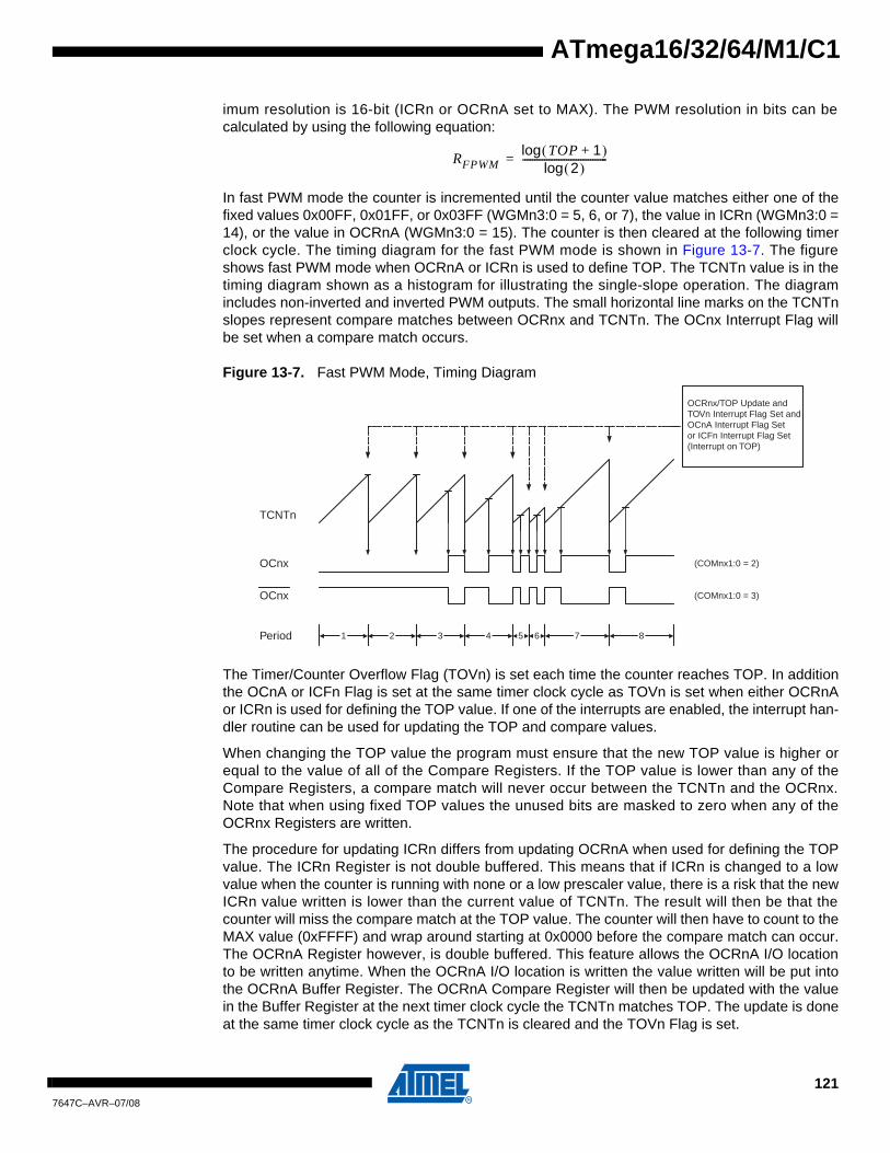
ATmega16/32/64/M1/C1
imum resolution is 16-bit (ICRn or OCRnA set to MAX). The PWM resolution in bits can becalculated by using the following equation:
In fast PWM mode the counter is incremented until the counter value matches either one of thefixed values 0x00FF, 0x01FF, or 0x03FF (WGMn3:0 = 5, 6, or 7), the value in ICRn (WGMn3:0 =14), or the value in OCRnA (WGMn3:0 = 15). The counter is then cleared at the following timerclock cycle. The timing diagram for the fast PWM mode is shown in Figure 13-7. The figureshows fast PWM mode when OCRnA or ICRn is used to define TOP. The TCNTn value is in thetiming diagram shown as a histogram for illustrating the single-slope operation. The diagramincludes non-inverted and inverted PWM outputs. The small horizontal line marks on the TCNTnslopes represent compare matches between OCRnx and TCNTn. The OCnx Interrupt Flag willbe set when a compare match occurs.
Figure 13-7. Fast PWM Mode, Timing Diagram
The Timer/Counter Overflow Flag (TOVn) is set each time the counter reaches TOP. In additionthe OCnA or ICFn Flag is set at the same timer clock cycle as TOVn is set when either OCRnAor ICRn is used for defining the TOP value. If one of the interrupts are enabled, the interrupt han-dler routine can be used for updating the TOP and compare values.
When changing the TOP value the program must ensure that the new TOP value is higher orequal to the value of all of the Compare Registers. If the TOP value is lower than any of theCompare Registers, a compare match will never occur between the TCNTn and the OCRnx.Note that when using fixed TOP values the unused bits are masked to zero when any of theOCRnx Registers are written.
The procedure for updating ICRn differs from updating OCRnA when used for defining the TOPvalue. The ICRn Register is not double buffered. This means that if ICRn is changed to a lowvalue when the counter is running with none or a low prescaler value, there is a risk that the newICRn value written is lower than the current value of TCNTn. The result will then be that thecounter will miss the compare match at the TOP value. The counter will then have to count to theMAX value (0xFFFF) and wrap around starting at 0x0000 before the compare match can occur.The OCRnA Register however, is double buffered. This feature allows the OCRnA I/O locationto be written anytime. When the OCRnA I/O location is written the value written will be put intothe OCRnA Buffer Register. The OCRnA Compare Register will then be updated with the valuein the Buffer Register at the next timer clock cycle the TCNTn matches TOP. The update is doneat the same timer clock cycle as the TCNTn is cleared and the TOVn Flag is set.
RFPWMTOP 1+( )log
2( )log-----------------------------------=
TCNTn
OCRnx/TOP Update andTOVn Interrupt Flag Set andOCnA Interrupt Flag Setor ICFn Interrupt Flag Set(Interrupt on TOP)
1 7Period 2 3 4 5 6 8
OCnx
OCnx
(COMnx1:0 = 2)
(COMnx1:0 = 3)
1217647C–AVR–07/08

Using the ICRn Register for defining TOP works well when using fixed TOP values. By usingICRn, the OCRnA Register is free to be used for generating a PWM output on OCnA. However,if the base PWM frequency is actively changed (by changing the TOP value), using the OCRnAas TOP is clearly a better choice due to its double buffer feature.
In fast PWM mode, the compare units allow generation of PWM waveforms on the OCnx pins.Setting the COMnx1:0 bits to two will produce a non-inverted PWM and an inverted PWM outputcan be generated by setting the COMnx1:0 to three (see Table on page 128). The actual OCnxvalue will only be visible on the port pin if the data direction for the port pin is set as output(DDR_OCnx). The PWM waveform is generated by setting (or clearing) the OCnx Register atthe compare match between OCRnx and TCNTn, and clearing (or setting) the OCnx Register atthe timer clock cycle the counter is cleared (changes from TOP to BOTTOM).
The PWM frequency for the output can be calculated by the following equation:
The N variable represents the prescaler divider (1, 8, 64, 256, or 1024).
The extreme values for the OCRnx Register represents special cases when generating a PWMwaveform output in the fast PWM mode. If the OCRnx is set equal to BOTTOM (0x0000) the out-put will be a narrow spike for each TOP+1 timer clock cycle. Setting the OCRnx equal to TOPwill result in a constant high or low output (depending on the polarity of the output set by theCOMnx1:0 bits.)
A frequency (with 50% duty cycle) waveform output in fast PWM mode can be achieved by set-ting OCnA to toggle its logical level on each compare match (COMnA1:0 = 1). This applies onlyif OCR1A is used to define the TOP value (WGM13:0 = 15). The waveform generated will havea maximum frequency of fOCnA = fclk_I/O/2 when OCRnA is set to zero (0x0000). This feature issimilar to the OCnA toggle in CTC mode, except the double buffer feature of the Output Com-pare unit is enabled in the fast PWM mode.
13.8.4 Phase Correct PWM Mode
The phase correct Pulse Width Modulation or phase correct PWM mode (WGMn3:0 = 1, 2, 3,10, or 11) provides a high resolution phase correct PWM waveform generation option. Thephase correct PWM mode is, like the phase and frequency correct PWM mode, based on a dual-slope operation. The counter counts repeatedly from BOTTOM (0x0000) to TOP and then fromTOP to BOTTOM. In non-inverting Compare Output mode, the Output Compare (OCnx) iscleared on the compare match between TCNTn and OCRnx while upcounting, and set on thecompare match while downcounting. In inverting Output Compare mode, the operation isinverted. The dual-slope operation has lower maximum operation frequency than single slopeoperation. However, due to the symmetric feature of the dual-slope PWM modes, these modesare preferred for motor control applications.
The PWM resolution for the phase correct PWM mode can be fixed to 8-, 9-, or 10-bit, or definedby either ICRn or OCRnA. The minimum resolution allowed is 2-bit (ICRn or OCRnA set to0x0003), and the maximum resolution is 16-bit (ICRn or OCRnA set to MAX). The PWM resolu-tion in bits can be calculated by using the following equation:
In phase correct PWM mode the counter is incremented until the counter value matches eitherone of the fixed values 0x00FF, 0x01FF, or 0x03FF (WGMn3:0 = 1, 2, or 3), the value in ICRn(WGMn3:0 = 10), or the value in OCRnA (WGMn3:0 = 11). The counter has then reached the
fOCnxPWMfclk_I/O
N 1 TOP+( )⋅-----------------------------------=
RPCPWMTOP 1+( )log
2( )log-----------------------------------=
1227647C–AVR–07/08
ATmega16/32/64/M1/C1

ATmega16/32/64/M1/C1
TOP and changes the count direction. The TCNTn value will be equal to TOP for one timer clockcycle. The timing diagram for the phase correct PWM mode is shown on Figure 13-8. The figureshows phase correct PWM mode when OCRnA or ICRn is used to define TOP. The TCNTnvalue is in the timing diagram shown as a histogram for illustrating the dual-slope operation. Thediagram includes non-inverted and inverted PWM outputs. The small horizontal line marks onthe TCNTn slopes represent compare matches between OCRnx and TCNTn. The OCnx Inter-rupt Flag will be set when a compare match occurs.
Figure 13-8. Phase Correct PWM Mode, Timing Diagram
The Timer/Counter Overflow Flag (TOVn) is set each time the counter reaches BOTTOM. Wheneither OCRnA or ICRn is used for defining the TOP value, the OCnA or ICFn Flag is set accord-ingly at the same timer clock cycle as the OCRnx Registers are updated with the double buffervalue (at TOP). The Interrupt Flags can be used to generate an interrupt each time the counterreaches the TOP or BOTTOM value.
When changing the TOP value the program must ensure that the new TOP value is higher orequal to the value of all of the Compare Registers. If the TOP value is lower than any of theCompare Registers, a compare match will never occur between the TCNTn and the OCRnx.Note that when using fixed TOP values, the unused bits are masked to zero when any of theOCRnx Registers are written. As the third period shown in Figure 13-8 illustrates, changing theTOP actively while the Timer/Counter is running in the phase correct mode can result in anunsymmetrical output. The reason for this can be found in the time of update of the OCRnx Reg-ister. Since the OCRnx update occurs at TOP, the PWM period starts and ends at TOP. Thisimplies that the length of the falling slope is determined by the previous TOP value, while thelength of the rising slope is determined by the new TOP value. When these two values differ thetwo slopes of the period will differ in length. The difference in length gives the unsymmetricalresult on the output.
It is recommended to use the phase and frequency correct mode instead of the phase correctmode when changing the TOP value while the Timer/Counter is running. When using a staticTOP value there are practically no differences between the two modes of operation.
In phase correct PWM mode, the compare units allow generation of PWM waveforms on theOCnx pins. Setting the COMnx1:0 bits to two will produce a non-inverted PWM and an invertedPWM output can be generated by setting the COMnx1:0 to three (See Table on page 128). The
OCRnx/TOP Update andOCnA Interrupt Flag Setor ICFn Interrupt Flag Set(Interrupt on TOP)
1 2 3 4
TOVn Interrupt Flag Set(Interrupt on Bottom)
TCNTn
Period
OCnx
OCnx
(COMnx1:0 = 2)
(COMnx1:0 = 3)
1237647C–AVR–07/08

actual OCnx value will only be visible on the port pin if the data direction for the port pin is set asoutput (DDR_OCnx). The PWM waveform is generated by setting (or clearing) the OCnx Regis-ter at the compare match between OCRnx and TCNTn when the counter increments, andclearing (or setting) the OCnx Register at compare match between OCRnx and TCNTn whenthe counter decrements. The PWM frequency for the output when using phase correct PWM canbe calculated by the following equation:
The N variable represents the prescaler divider (1, 8, 64, 256, or 1024).
The extreme values for the OCRnx Register represent special cases when generating a PWMwaveform output in the phase correct PWM mode. If the OCRnx is set equal to BOTTOM theoutput will be continuously low and if set equal to TOP the output will be continuously high fornon-inverted PWM mode. For inverted PWM the output will have the opposite logic values. IfOCR1A is used to define the TOP value (WGM13:0 = 11) and COM1A1:0 = 1, the OC1A outputwill toggle with a 50% duty cycle.
13.8.5 Phase and Frequency Correct PWM Mode
The phase and frequency correct Pulse Width Modulation, or phase and frequency correct PWMmode (WGMn3:0 = 8 or 9) provides a high resolution phase and frequency correct PWM wave-form generation option. The phase and frequency correct PWM mode is, like the phase correctPWM mode, based on a dual-slope operation. The counter counts repeatedly from BOTTOM(0x0000) to TOP and then from TOP to BOTTOM. In non-inverting Compare Output mode, theOutput Compare (OCnx) is cleared on the compare match between TCNTn and OCRnx whileupcounting, and set on the compare match while downcounting. In inverting Compare Outputmode, the operation is inverted. The dual-slope operation gives a lower maximum operation fre-quency compared to the single-slope operation. However, due to the symmetric feature of thedual-slope PWM modes, these modes are preferred for motor control applications.
The main difference between the phase correct, and the phase and frequency correct PWMmode is the time the OCRnx Register is updated by the OCRnx Buffer Register, (see Figure 13-8 and Figure 13-9).
The PWM resolution for the phase and frequency correct PWM mode can be defined by eitherICRn or OCRnA. The minimum resolution allowed is 2-bit (ICRn or OCRnA set to 0x0003), andthe maximum resolution is 16-bit (ICRn or OCRnA set to MAX). The PWM resolution in bits canbe calculated using the following equation:
In phase and frequency correct PWM mode the counter is incremented until the counter valuematches either the value in ICRn (WGMn3:0 = 8), or the value in OCRnA (WGMn3:0 = 9). Thecounter has then reached the TOP and changes the count direction. The TCNTn value will beequal to TOP for one timer clock cycle. The timing diagram for the phase correct and frequencycorrect PWM mode is shown on Figure 13-9. The figure shows phase and frequency correctPWM mode when OCRnA or ICRn is used to define TOP. The TCNTn value is in the timing dia-gram shown as a histogram for illustrating the dual-slope operation. The diagram includes non-inverted and inverted PWM outputs. The small horizontal line marks on the TCNTn slopes repre-sent compare matches between OCRnx and TCNTn. The OCnx Interrupt Flag will be set when acompare match occurs.
fOCnxPCPWMfclk_I/O
2 N TOP⋅ ⋅----------------------------=
RPFCPWMTOP 1+( )log
2( )log-----------------------------------=
1247647C–AVR–07/08
ATmega16/32/64/M1/C1

ATmega16/32/64/M1/C1
Figure 13-9. Phase and Frequency Correct PWM Mode, Timing Diagram
The Timer/Counter Overflow Flag (TOVn) is set at the same timer clock cycle as the OCRnxRegisters are updated with the double buffer value (at BOTTOM). When either OCRnA or ICRnis used for defining the TOP value, the OCnA or ICFn Flag is set when TCNTn has reachedTOP. The Interrupt Flags can then be used to generate an interrupt each time the counterreaches the TOP or BOTTOM value.
When changing the TOP value the program must ensure that the new TOP value is higher orequal to the value of all of the Compare Registers. If the TOP value is lower than any of theCompare Registers, a compare match will never occur between the TCNTn and the OCRnx.
As Figure 13-9 shows the output generated is, in contrast to the phase correct mode, symmetri-cal in all periods. Since the OCRnx Registers are updated at BOTTOM, the length of the risingand the falling slopes will always be equal. This gives symmetrical output pulses and is thereforefrequency correct.
Using the ICRn Register for defining TOP works well when using fixed TOP values. By usingICRn, the OCRnA Register is free to be used for generating a PWM output on OCnA. However,if the base PWM frequency is actively changed by changing the TOP value, using the OCRnA asTOP is clearly a better choice due to its double buffer feature.
In phase and frequency correct PWM mode, the compare units allow generation of PWM wave-forms on the OCnx pins. Setting the COMnx1:0 bits to two will produce a non-inverted PWM andan inverted PWM output can be generated by setting the COMnx1:0 to three (See Table onpage 128). The actual OCnx value will only be visible on the port pin if the data direction for theport pin is set as output (DDR_OCnx). The PWM waveform is generated by setting (or clearing)the OCnx Register at the compare match between OCRnx and TCNTn when the counter incre-ments, and clearing (or setting) the OCnx Register at compare match between OCRnx andTCNTn when the counter decrements. The PWM frequency for the output when using phaseand frequency correct PWM can be calculated by the following equation:
The N variable represents the prescaler divider (1, 8, 64, 256, or 1024).
OCRnx/TOP UpdateandTOVn Interrupt Flag Set(Interrupt on Bottom)
OCnA Interrupt Flag Setor ICFn Interrupt Flag Set(Interrupt on TOP)
1 2 3 4
TCNTn
Period
OCnx
OCnx
(COMnx1:0 = 2)
(COMnx1:0 = 3)
fOCnxPFCPWMfclk_I/O
2 N TOP⋅ ⋅----------------------------=
1257647C–AVR–07/08

The extreme values for the OCRnx Register represents special cases when generating a PWMwaveform output in the phase correct PWM mode. If the OCRnx is set equal to BOTTOM theoutput will be continuously low and if set equal to TOP the output will be set to high for non-inverted PWM mode. For inverted PWM the output will have the opposite logic values. If OCR1Ais used to define the TOP value (WGM13:0 = 9) and COM1A1:0 = 1, the OC1A output will togglewith a 50% duty cycle.
13.9 Timer/Counter Timing DiagramsThe Timer/Counter is a synchronous design and the timer clock (clkTn) is therefore shown as aclock enable signal in the following figures. The figures include information on when InterruptFlags are set, and when the OCRnx Register is updated with the OCRnx buffer value (only formodes utilizing double buffering). Figure 13-10 shows a timing diagram for the setting of OCFnx.
Figure 13-10. Timer/Counter Timing Diagram, Setting of OCFnx, no Prescaling
Figure 13-11 shows the same timing data, but with the prescaler enabled.
Figure 13-11. Timer/Counter Timing Diagram, Setting of OCFnx, with Prescaler (fclk_I/O/8)
Figure 13-12 shows the count sequence close to TOP in various modes. When using phase andfrequency correct PWM mode the OCRnx Register is updated at BOTTOM. The timing diagramswill be the same, but TOP should be replaced by BOTTOM, TOP-1 by BOTTOM+1 and so on.The same renaming applies for modes that set the TOVn Flag at BOTTOM.
clkTn(clkI/O/1)
OCFnx
clkI/O
OCRnx
TCNTn
OCRnx Value
OCRnx - 1 OCRnx OCRnx + 1 OCRnx + 2
OCFnx
OCRnx
TCNTn
OCRnx Value
OCRnx - 1 OCRnx OCRnx + 1 OCRnx + 2
clkI/O
clkTn(clkI/O/8)
1267647C–AVR–07/08
ATmega16/32/64/M1/C1
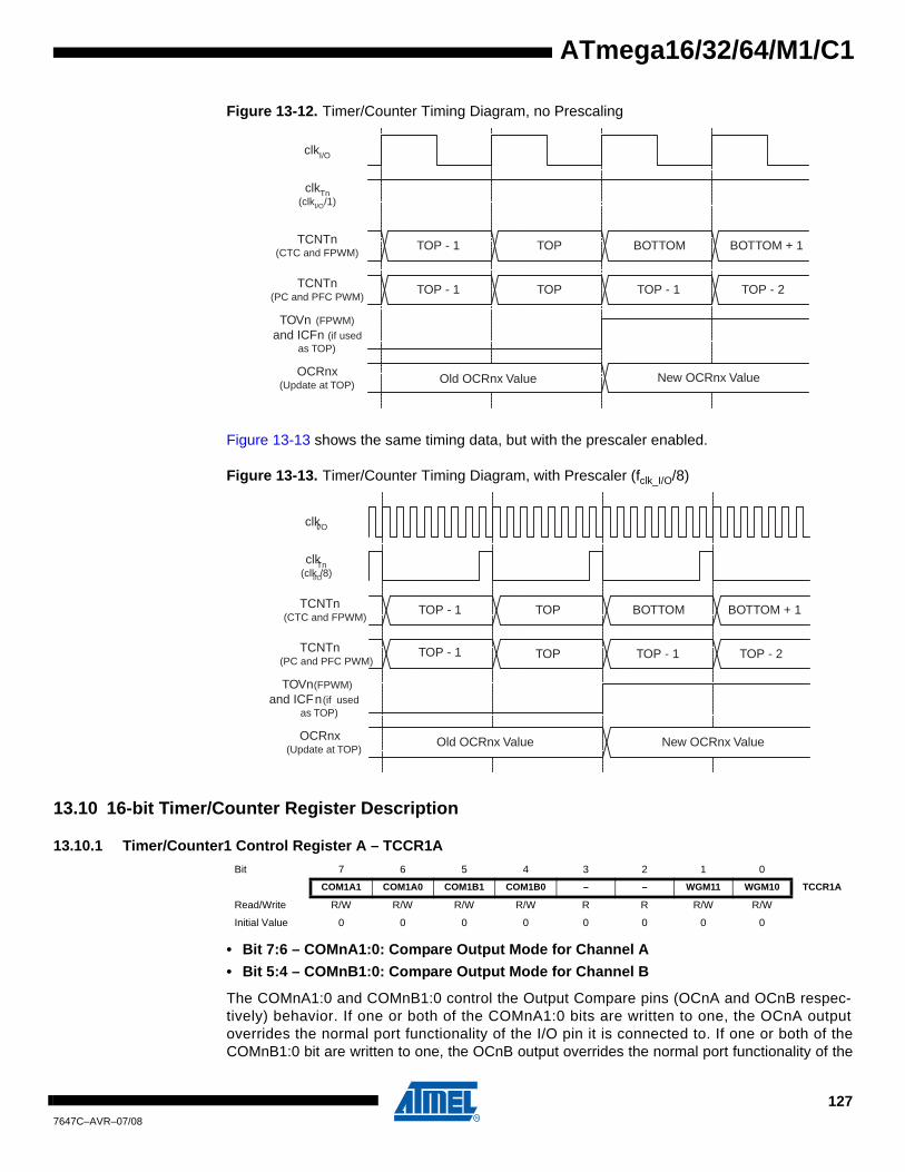
ATmega16/32/64/M1/C1
Figure 13-12. Timer/Counter Timing Diagram, no Prescaling
Figure 13-13 shows the same timing data, but with the prescaler enabled.
Figure 13-13. Timer/Counter Timing Diagram, with Prescaler (fclk_I/O/8)
13.10 16-bit Timer/Counter Register Description
13.10.1 Timer/Counter1 Control Register A – TCCR1A
• Bit 7:6 – COMnA1:0: Compare Output Mode for Channel A• Bit 5:4 – COMnB1:0: Compare Output Mode for Channel B
The COMnA1:0 and COMnB1:0 control the Output Compare pins (OCnA and OCnB respec-tively) behavior. If one or both of the COMnA1:0 bits are written to one, the OCnA outputoverrides the normal port functionality of the I/O pin it is connected to. If one or both of theCOMnB1:0 bit are written to one, the OCnB output overrides the normal port functionality of the
TOVn (FPWM)and ICFn (if used
as TOP)
OCRnx(Update at TOP)
TCNTn(CTC and FPWM)
TCNTn(PC and PFC PWM)
TOP - 1 TOP TOP - 1 TOP - 2
Old OCRnx Value New OCRnx Value
TOP - 1 TOP BOTTOM BOTTOM + 1
clkTn(clkI/O/1)
clkI/O
TOVn (FPWM)and ICFn (if used
as TOP)
OCRnx(Update at TOP)
TCNTn(CTC and FPWM)
TCNTn(PC and PFC PWM)
TOP - 1 TOP TOP - 1 TOP - 2
Old OCRnx Value New OCRnx Value
TOP - 1 TOP BOTTOM BOTTOM + 1
clkI/O
clkTn(clkI/O/8)
Bit 7 6 5 4 3 2 1 0
COM1A1 COM1A0 COM1B1 COM1B0 – – WGM11 WGM10 TCCR1A
Read/Write R/W R/W R/W R/W R R R/W R/W
Initial Value 0 0 0 0 0 0 0 0
1277647C–AVR–07/08

I/O pin it is connected to. However, note that the Data Direction Register (DDR) bit correspond-ing to the OCnA or OCnB pin must be set in order to enable the output driver.
When the OCnA or OCnB is connected to the pin, the function of the COMnx1:0 bits is depen-dent of the WGMn3:0 bits setting. Table 13-1 shows the COMnx1:0 bit functionality when theWGMn3:0 bits are set to a Normal or a CTC mode (non-PWM).
Table 13-2 shows the COMnx1:0 bit functionality when the WGMn3:0 bits are set to the fastPWM mode.
Note: 1. A special case occurs when OCRnA/OCRnB equals TOP and COMnA1/COMnB1 is set. Inthis case the compare match is ignored, but the set or clear is done at TOP. See “Fast PWMMode” on page 120. for more details.
Table 13-3 shows the COMnx1:0 bit functionality when the WGMn3:0 bits are set to the phasecorrect or the phase and frequency correct, PWM mode.
Table 13-1. Compare Output Mode, non-PWM
COMnA1/COMnB1 COMnA0/COMnB0 Description
0 0 Normal port operation, OCnA/OCnB disconnected.
0 1 Toggle OCnA/OCnB on Compare Match.
1 0 Clear OCnA/OCnB on Compare Match (Set output to low level).
1 1 Set OCnA/OCnB on Compare Match (Set output to high level).
Table 13-2. Compare Output Mode, Fast PWM(1)
COMnA1/COMnB1 COMnA0/COMnB0 Description
0 0 Normal port operation, OCnA/OCnB disconnected.
0 1
WGMn3:0 = 14 or 15: Toggle OC1A on Compare Match, OC1B disconnected (normal port operation). For all other WGM1 settings, normal port operation, OC1A/OC1B disconnected.
1 0 Clear OCnA/OCnB on Compare Match, set OCnA/OCnB at TOP
1 1 Set OCnA/OCnB on Compare Match, clear OCnA/OCnB at TOP
Table 13-3. Compare Output Mode, Phase Correct and Phase and Frequency Correct PWM(1)
COMnA1/COMnB1 COMnA0/COMnB0 Description
0 0 Normal port operation, OCnA/OCnB disconnected.
1287647C–AVR–07/08
ATmega16/32/64/M1/C1
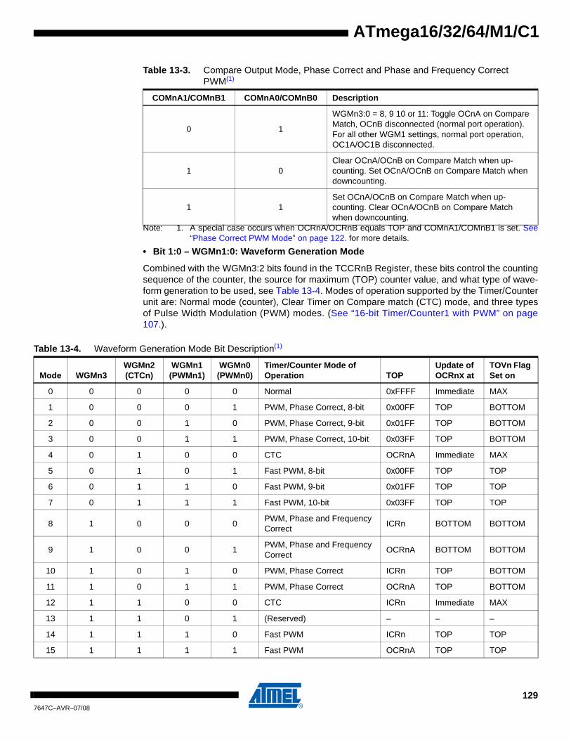
ATmega16/32/64/M1/C1
Note: 1. A special case occurs when OCRnA/OCRnB equals TOP and COMnA1/COMnB1 is set. See“Phase Correct PWM Mode” on page 122. for more details.
• Bit 1:0 – WGMn1:0: Waveform Generation Mode
Combined with the WGMn3:2 bits found in the TCCRnB Register, these bits control the countingsequence of the counter, the source for maximum (TOP) counter value, and what type of wave-form generation to be used, see Table 13-4. Modes of operation supported by the Timer/Counterunit are: Normal mode (counter), Clear Timer on Compare match (CTC) mode, and three typesof Pulse Width Modulation (PWM) modes. (See “16-bit Timer/Counter1 with PWM” on page107.).
0 1
WGMn3:0 = 8, 9 10 or 11: Toggle OCnA on Compare Match, OCnB disconnected (normal port operation). For all other WGM1 settings, normal port operation, OC1A/OC1B disconnected.
1 0Clear OCnA/OCnB on Compare Match when up-counting. Set OCnA/OCnB on Compare Match when downcounting.
1 1Set OCnA/OCnB on Compare Match when up-counting. Clear OCnA/OCnB on Compare Match when downcounting.
Table 13-3. Compare Output Mode, Phase Correct and Phase and Frequency Correct PWM(1)
COMnA1/COMnB1 COMnA0/COMnB0 Description
Table 13-4. Waveform Generation Mode Bit Description(1)
Mode WGMn3WGMn2(CTCn)
WGMn1(PWMn1)
WGMn0(PWMn0)
Timer/Counter Mode of Operation TOP
Update of OCRnx at
TOVn Flag Set on
0 0 0 0 0 Normal 0xFFFF Immediate MAX
1 0 0 0 1 PWM, Phase Correct, 8-bit 0x00FF TOP BOTTOM
2 0 0 1 0 PWM, Phase Correct, 9-bit 0x01FF TOP BOTTOM
3 0 0 1 1 PWM, Phase Correct, 10-bit 0x03FF TOP BOTTOM
4 0 1 0 0 CTC OCRnA Immediate MAX
5 0 1 0 1 Fast PWM, 8-bit 0x00FF TOP TOP
6 0 1 1 0 Fast PWM, 9-bit 0x01FF TOP TOP
7 0 1 1 1 Fast PWM, 10-bit 0x03FF TOP TOP
8 1 0 0 0 PWM, Phase and Frequency Correct ICRn BOTTOM BOTTOM
9 1 0 0 1 PWM, Phase and Frequency Correct OCRnA BOTTOM BOTTOM
10 1 0 1 0 PWM, Phase Correct ICRn TOP BOTTOM
11 1 0 1 1 PWM, Phase Correct OCRnA TOP BOTTOM
12 1 1 0 0 CTC ICRn Immediate MAX
13 1 1 0 1 (Reserved) – – –
14 1 1 1 0 Fast PWM ICRn TOP TOP
15 1 1 1 1 Fast PWM OCRnA TOP TOP
1297647C–AVR–07/08

Note: 1. The CTCn and PWMn1:0 bit definition names are obsolete. Use the WGMn2:0 definitions. However, the functionality andlocation of these bits are compatible with previous versions of the timer.
13.10.2 Timer/Counter1 Control Register B – TCCR1B
• Bit 7 – ICNCn: Input Capture Noise Canceler
Setting this bit (to one) activates the Input Capture Noise Canceler. When the noise canceler isactivated, the input from the Input Capture pin (ICPn) is filtered. The filter function requires foursuccessive equal valued samples of the ICPn pin for changing its output. The Input Capture istherefore delayed by four Oscillator cycles when the noise canceler is enabled.• Bit 6 – ICESn: Input Capture Edge Select
This bit selects which edge on the Input Capture pin (ICPn) that is used to trigger a captureevent. When the ICESn bit is written to zero, a falling (negative) edge is used as trigger, andwhen the ICESn bit is written to one, a rising (positive) edge will trigger the capture.
When a capture is triggered according to the ICESn setting, the counter value is copied into theInput Capture Register (ICRn). The event will also set the Input Capture Flag (ICFn), and thiscan be used to cause an Input Capture Interrupt, if this interrupt is enabled.
When the ICRn is used as TOP value (see description of the WGMn3:0 bits located in theTCCRnA and the TCCRnB Register), the ICPn is disconnected and consequently the Input Cap-ture function is disabled.• Bit 5 – RTGENSet this bit to enable the ICP1A as a timer/counter retrigger input.
(This bit is reserved for future use. For ensuring compatibility with future devices, this bit must bewritten to zero when TCCRnB is written.)• Bit 4:3 – WGMn3:2: Waveform Generation Mode
See TCCRnA Register description.• Bit 2:0 – CSn2:0: Clock Select
The three Clock Select bits select the clock source to be used by the Timer/Counter, see Figure13-10 and Figure 13-11.
Bit 7 6 5 4 3 2 1 0
ICNC1 ICES1 RTGEN WGM13 WGM12 CS12 CS11 CS10 TCCR1BRead/Write R/W R/W R R/W R/W R/W R/W R/W
Initial Value 0 0 0 0 0 0 0 0
Table 13-5. Clock Select Bit Description
CSn2 CSn1 CSn0 Description
0 0 0 No clock source (Timer/Counter stopped).
0 0 1 clkI/O/1 (No prescaling)
0 1 0 clkI/O/8 (From prescaler)
0 1 1 clkI/O/64 (From prescaler)
1 0 0 clkI/O/256 (From prescaler)
1 0 1 clkI/O/1024 (From prescaler)
1 1 0 External clock source on Tn pin. Clock on falling edge.
1 1 1 External clock source on Tn pin. Clock on rising edge.
1307647C–AVR–07/08
ATmega16/32/64/M1/C1

ATmega16/32/64/M1/C1
If external pin modes are used for the Timer/Countern, transitions on the Tn pin will clock thecounter even if the pin is configured as an output. This feature allows software control of thecounting.
13.10.3 Timer/Counter1 Control Register C – TCCR1C
• Bit 7 – FOCnA: Force Output Compare for Channel A• Bit 6 – FOCnB: Force Output Compare for Channel B
The FOCnA/FOCnB bits are only active when the WGMn3:0 bits specifies a non-PWM mode.However, for ensuring compatibility with future devices, these bits must be set to zero whenTCCRnA is written when operating in a PWM mode. When writing a logical one to theFOCnA/FOCnB bit, an immediate compare match is forced on the Waveform Generation unit.The OCnA/OCnB output is changed according to its COMnx1:0 bits setting. Note that theFOCnA/FOCnB bits are implemented as strobes. Therefore it is the value present in theCOMnx1:0 bits that determine the effect of the forced compare.
A FOCnA/FOCnB strobe will not generate any interrupt nor will it clear the timer in Clear Timeron Compare match (CTC) mode using OCRnA as TOP.
The FOCnA/FOCnB bits are always read as zero.
13.10.4 Timer/Counter1 – TCNT1H and TCNT1L
The two Timer/Counter I/O locations (TCNTnH and TCNTnL, combined TCNTn) give directaccess, both for read and for write operations, to the Timer/Counter unit 16-bit counter. Toensure that both the high and low bytes are read and written simultaneously when the CPUaccesses these registers, the access is performed using an 8-bit temporary High Byte Register(TEMP). This temporary register is shared by all the other 16-bit registers. See “Accessing 16-bitRegisters” on page 109.
Modifying the counter (TCNTn) while the counter is running introduces a risk of missing a com-pare match between TCNTn and one of the OCRnx Registers.
Writing to the TCNTn Register blocks (removes) the compare match on the following timer clockfor all compare units.
13.10.5 Output Compare Register 1 A – OCR1AH and OCR1AL
Bit 7 6 5 4 3 2 1 0
FOC1A FOC1B – – – – – – TCCR1CRead/Write R/W R/W R R R R R R
Initial Value 0 0 0 0 0 0 0 0
Bit 7 6 5 4 3 2 1 0
TCNT1[15:8] TCNT1HTCNT1[7:0] TCNT1L
Read/Write R/W R/W R/W R/W R/W R/W R/W R/W
Initial Value 0 0 0 0 0 0 0 0
Bit 7 6 5 4 3 2 1 0
OCR1A[15:8] OCR1AHOCR1A[7:0] OCR1AL
Read/Write R/W R/W R/W R/W R/W R/W R/W R/W
Initial Value 0 0 0 0 0 0 0 0
1317647C–AVR–07/08

13.10.6 Output Compare Register 1 B – OCR1BH and OCR1BL
The Output Compare Registers contain a 16-bit value that is continuously compared with thecounter value (TCNTn). A match can be used to generate an Output Compare interrupt, or togenerate a waveform output on the OCnx pin.
The Output Compare Registers are 16-bit in size. To ensure that both the high and low bytes arewritten simultaneously when the CPU writes to these registers, the access is performed using an8-bit temporary High Byte Register (TEMP). This temporary register is shared by all the other16-bit registers. See “Accessing 16-bit Registers” on page 109.
Bit 7 6 5 4 3 2 1 0
OCR1B[15:8] OCR1BHOCR1B[7:0] OCR1BL
Read/Write R/W R/W R/W R/W R/W R/W R/W R/W
Initial Value 0 0 0 0 0 0 0 0
1327647C–AVR–07/08
ATmega16/32/64/M1/C1

ATmega16/32/64/M1/C1
13.10.7 Input Capture Register 1 – ICR1H and ICR1L
The Input Capture is updated with the counter (TCNTn) value each time an event occurs on theICPn pin (or optionally on the Analog Comparator output for Timer/Counter1). The Input Capturecan be used for defining the counter TOP value.
The Input Capture Register is 16-bit in size. To ensure that both the high and low bytes are readsimultaneously when the CPU accesses these registers, the access is performed using an 8-bittemporary High Byte Register (TEMP). This temporary register is shared by all the other 16-bitregisters. See “Accessing 16-bit Registers” on page 109.
13.10.8 Timer/Counter1 Interrupt Mask Register – TIMSK1
• Bit 7, 6 – Res: Reserved Bits
These bits are unused bits in the ATmega16/32/64/M1/C1, and will always read as zero.• Bit 5 – ICIE1: Timer/Counter1, Input Capture Interrupt Enable
When this bit is written to one, and the I-flag in the Status Register is set (interrupts globallyenabled), the Timer/Counter1 Input Capture interrupt is enabled. The corresponding InterruptVector (see “Reset and Interrupt Vectors Placement in AT90PWM324(1)” on page 54) is exe-cuted when the ICF1 Flag, located in TIFR1, is set.• Bit 4, 3 – Res: Reserved Bits
These bits are unused bits in the ATmega16/32/64/M1/C1, and will always read as zero.• Bit 2 – OCIE1B: Timer/Counter1, Output Compare B Match Interrupt Enable
When this bit is written to one, and the I-flag in the Status Register is set (interrupts globallyenabled), the Timer/Counter1 Output Compare B Match interrupt is enabled. The correspondingInterrupt Vector (see “Reset and Interrupt Vectors Placement in AT90PWM324(1)” on page 54) isexecuted when the OCF1B Flag, located in TIFR1, is set.• Bit 1 – OCIE1A: Timer/Counter1, Output Compare A Match Interrupt Enable
When this bit is written to one, and the I-flag in the Status Register is set (interrupts globallyenabled), the Timer/Counter1 Output Compare A Match interrupt is enabled. The correspondingInterrupt Vector (see “Reset and Interrupt Vectors Placement in AT90PWM324(1)” on page 54) isexecuted when the OCF1A Flag, located in TIFR1, is set.• Bit 0 – TOIE1: Timer/Counter1, Overflow Interrupt Enable
When this bit is written to one, and the I-flag in the Status Register is set (interrupts globallyenabled), the Timer/Counter1 Overflow interrupt is enabled. The corresponding Interrupt Vector(see “Reset and Interrupt Vectors Placement in AT90PWM324(1)” on page 54) is executed whenthe TOV1 Flag, located in TIFR1, is set.
Bit 7 6 5 4 3 2 1 0
ICR1[15:8] ICR1HICR1[7:0] ICR1L
Read/Write R/W R/W R/W R/W R/W R/W R/W R/W
Initial Value 0 0 0 0 0 0 0 0
Bit 7 6 5 4 3 2 1 0
– – ICIE1 – – OCIE1B OCIE1A TOIE1 TIMSK1Read/Write R R R/W R R R/W R/W R/W
Initial Value 0 0 0 0 0 0 0 0
1337647C–AVR–07/08

13.10.9 Timer/Counter1 Interrupt Flag Register – TIFR1
• Bit 7, 6 – Res: Reserved Bits
These bits are unused bits in the ATmega16/32/64/M1/C1, and will always read as zero.• Bit 5 – ICF1: Timer/Counter1, Input Capture Flag
This flag is set when a capture event occurs on the ICP1 pin. When the Input Capture Register(ICR1) is set by the WGMn3:0 to be used as the TOP value, the ICF1 Flag is set when thecounter reaches the TOP value.
ICF1 is automatically cleared when the Input Capture Interrupt Vector is executed. Alternatively,ICF1 can be cleared by writing a logic one to its bit location.• Bit 4, 3 – Res: Reserved Bits
These bits are unused bits in the ATmega16/32/64/M1/C1, and will always read as zero.• Bit 2 – OCF1B: Timer/Counter1, Output Compare B Match Flag
This flag is set in the timer clock cycle after the counter (TCNT1) value matches the OutputCompare Register B (OCR1B).
Note that a Forced Output Compare (FOC1B) strobe will not set the OCF1B Flag.
OCF1B is automatically cleared when the Output Compare Match B Interrupt Vector is exe-cuted. Alternatively, OCF1B can be cleared by writing a logic one to its bit location.• Bit 1 – OCF1A: Timer/Counter1, Output Compare A Match Flag
This flag is set in the timer clock cycle after the counter (TCNT1) value matches the OutputCompare Register A (OCR1A).
Note that a Forced Output Compare (FOC1A) strobe will not set the OCF1A Flag.
OCF1A is automatically cleared when the Output Compare Match A Interrupt Vector is exe-cuted. Alternatively, OCF1A can be cleared by writing a logic one to its bit location.• Bit 0 – TOV1: Timer/Counter1, Overflow Flag
The setting of this flag is dependent of the WGMn3:0 bits setting. In Normal and CTC modes,the TOV1 Flag is set when the timer overflows. Refer to Table 13-4 on page 129 for the TOV1Flag behavior when using another WGMn3:0 bit setting.
TOV1 is automatically cleared when the Timer/Counter1 Overflow Interrupt Vector is executed.Alternatively, TOV1 can be cleared by writing a logic one to its bit location.
Bit 7 6 5 4 3 2 1 0
– – ICF1 – – OCF1B OCF1A TOV1 TIFR1Read/Write R R R/W R R R/W R/W R/W
Initial Value 0 0 0 0 0 0 0 0
1347647C–AVR–07/08
ATmega16/32/64/M1/C1

ATmega16/32/64/M1/C1
14. Power Stage Controller – (PSC) (only ATmega16/32/64M1)The Power Stage Controller is a high performance waveform controller.
14.1 Features• PWM waveform generation function with 6 complementary programmable outputs (able to
control 3 half-bridges)• Programmable dead time control• PWM up to 12 bit resolution• PWM clock frequency up to 64 MHz (via PLL)• Programmable ADC trigger• Automatic Overlap protection• Failsafe emergency inputs - 3 (to force all outputs to high impedance or in inactive state - fuse
configurable)• Center aligned and edge aligned modes synchronization
14.2 OverviewMany register and bit references in this section are written in general form.• A lower case “n” replaces the PSC module number, in this case 0, 1 or 2. However, when
using the register or bit defines in a program, the precise form must be used, i.e., POCR0SAH for accessing module 0 POCRnSAH register and so on.
• A lower case “x” replaces the PSC part , in this case A or B. However, when using the register or bit defines in a program, the precise form must be used, i.e., OCR0SAH for accessing part A OCR0SxH register and so on.
The purpose of the Power Stage Controller (PSC) is to control an external power interface. It hassix outputs to drive for example a 3 half-bridge. This feature allows you to generate three phasewaveforms for applications such as Asynchronous or BLDC motor drives, lighting systems...
The PSC also has 3 inputs, the purpose of which is to provide fast emergency stop capability.
The PSC outputs are programmable as “active high” or “active low”. All the timing diagrams inthe following examples are given in the “active high” polarity.
14.3 Accessing 16-bit RegistersSome PSC registers are 16-bit registers. These registers can be accessed by the AVR CPU viathe 8-bit data bus. The 16-bit registers must be byte accessed using two read or write opera-tions. The PSC has a single 8-bit register for temporary storing of the high byte of the 16-bitaccess. The same temporary register is shared between all PSC 16-bit registers. Accessing thelow byte triggers the 16-bit read or write operation. When the low byte of a 16-bit register is writ-ten by the CPU, the high byte stored in the temporary register, and the low byte written are bothcopied into the 16-bit register in the same clock cycle. When the low byte of a 16-bit register isread by the CPU, the high byte of the 16-bit register is copied into the temporary register in thesame clock cycle as the low byte is read.
To do a 16-bit write, the high byte must be written before the low byte. For a 16-bit read, the lowbyte must be read before the high byte.
1357647C–AVR–07/08

14.4 PSC Description
Figure 14-1. Power Stage Controller Block Diagram
DA
TAB
US
POCR0RB =
PSC Counter
WaveformGenerator B PSCOUT0B
PCTLn PFRCnA
PSOCn
(Analog Comparator 1 Ouput)
PCNFn PFRCnB
PSCIN1
PISEL1
PSC Input 1
POCR0SB =
POCR0RA =
POCR0SA =WaveformGenerator A PSCOUT0A
WaveformGenerator B PSCOUT1BPOCR1SB =
POCR1RA =
POCR1SA =WaveformGenerator A PSCOUT1A
WaveformGenerator B PSCOUT2BPOCR2SB =
POCR2RA =
POCR2SA =WaveformGenerator A PSCOUT2A
module 0
module 1
module 2
OverlapProtection
OverlapProtection
OverlapProtection
(Analog Comparator 0 Ouput)
PSCIN0
PISEL0
PSC Input 0
(Analog Comparator 2 Ouput)
PSCIN2
PISEL2
PSC Input 2
AC0O
AC1O
AC2O
Prescaler
CLKIO
CLKPLL
1367647C–AVR–07/08
ATmega16/32/64/M1/C1

ATmega16/32/64/M1/C1
The PSC is based on the use of a free-running 12-bit counter (PSC counter). This counter isable to count up to a top value determined by the contents of POCR_RB register and thenaccording to the selected running mode, count down or reset to zero for another cycle.
As can be seen from the block diagram Figure 14-1, the PSC is composed of 3 modules.
Each of the 3 PSC modules can be seen as two symetrical entities. One entity named part Awhich generates the output PSCOUTnA and the second one named part B which generates thePSCOUTnB output.
Each module has its own PSC Input circuitry which manages the corresponding input.
14.5 Functional Description
14.5.1 Generation of Control WaveformsIn general, the drive of a 3 phase motor requires the generation of 6 PWM signals. The dutycycle of these signals must be independently controlled to adjust the speed or torque of themotor or to produce the wanted waveform on the 3 voltage lines (trapezoidal, sinusoidal...)
In case of cross conduction or overtemperature, having inputs which can immediately disablethe waveform generator’s outputs is desirable.
These considerations are common for many systems which require PWM signals to drive powersystems such as lighting, DC/DC converters...
14.5.2 Waveform Cycles
Each of the 3 modules has 2 waveform generators which jointly compose the output signal.
The first part of the waveform is relative to part A or PSCOUTnA output. This waveform corre-sponds to sub-cycle A in the following figure.
The second part of the waveform is relative to part B or PSCOUTnB output. This waveform cor-responds to sub-cycle B in the following figure.
The complete waveform is terminated at the end of the sub-cycle B, whereupon any changes tothe settings of the waveform generator registers will be implemented, for the next cycle.
The PSC can be configured in one of two modes (1Ramp Mode or Centered Mode). This config-uration will affect the operation of all the waveform generators.
Figure 14-2. Cycle Presentation in One Ramp Mode
Sub-Cycle A Sub-Cycle B
One PSC Cycle
UPDATE
PSC Counter Value
1377647C–AVR–07/08

Figure 14-3. Cycle Presentation in Centered Mode
Figure 14-2 and Figure 14-3 graphically illustrate the values held in the PSC counter. CenteredMode is like One Ramp Mode which counts down and then up.
Notice that the update of the waveform generator registers is done regardless of ramp Mode atthe end of the PSC cycle.
14.5.3 Operation Mode Descriptions
Waveforms and duration of output signals are determined by parameters held in the registers(POCRnSA, POCRnRA, POCRnSB, POCR_RB) and by the running mode. Two modes are pos-sible :
– One Ramp Mode. In this mode, all the 3 PSCOUTnB outputs are edge-aligned and the 3 PSCOUTnA can be also edge-aligned when setting the same values in the dedicated registers.In this mode, the PWM frequency is twice the Center Aligned Mode PWM frequency.
– Center Aligned Mode. In this mode, all the 6 PSC outputs are aligned at the center of the period. Except when using the same duty cycles on the 3 modules, the edges of the outputs are not aligned. So the PSC outputs do not commute at the same time, thus the system which is driven by these outputs will generate less commutation noise.In this mode, the PWM frequency is twice slower than in One Ramp Mode.
14.5.3.1 One Ramp Mode (Edge-Aligned)
The following figure shows the resultant outputs PSCOUTnA and PSCOUTnB operating in oneramp mode over a PSC cycle.
One PSC Cycle
UPDATE
PSC Counter Value
1387647C–AVR–07/08
ATmega16/32/64/M1/C1

ATmega16/32/64/M1/C1
Figure 14-4. PSCOUTnA & PSCOUTnB Basic Waveforms in One Ramp mode
On-Time A = (POCRnRAH/L - POCRnSAH/L) * 1/Fclkpsc
On-Time B = (POCRnRBH/L - POCRnSBH/L) * 1/Fclkpsc
Dead-Time A = (POCRnSAH/L + 1) * 1/Fclkpsc
Dead-Time B = (POCRnSBH/L - POCRnRAH/L) * 1/FclkpscNote: Minimal value for Dead-Time A = 1/Fclkpsc
If the overlap protection is disabled, in One-Ramp mode, PSCOUTnA and PSCOUTnB outputscan be configured to overlap each other, though in normal use this is not desirable.
On-Time A On-Time B
PSCOUTnA
PSCOUTnB
Dead-Time BDead-Time A
PSC Cycle
POCRnRB
POCRnSB
POCRnRA
POCRnSA
PSC Counter
0
1397647C–AVR–07/08

Figure 14-5. Controlled Start and Stop Mechanism in One-Ramp Mode
Note: See “PSC Control Register – PCTL” on page 153. (PCCYC = 1)
14.5.3.2 Center Aligned Mode
In center aligned mode, the center of PSCOUTnA and PSCOUTnB signals are centered.
Figure 14-6. PSCOUTnA & PSCOUTnB Basic Waveforms in Center Aligned Mode
On-Time 0 = 2 * POCRnSAH/L * 1/Fclkpsc
On-Time 1 = 2 * (POCRnRBH/L - POCRnSBH/L + 1) * 1/Fclkpsc
Dead-Time = (POCRnSBH/L - POCRnSAH/L) * 1/Fclkpsc
PSCOUTnA
PSCOUTnB
PSC Counter
POCRnRB
POCRnRAPOCRnSB
0
Run
POCRnSA
On-Time 1
On-Time 0
PSCOUTnA
PSCOUTnB
PSC Cycle
Dead-Time
On-Time 1
Dead-Time
PSC CounterPOCRnRB
POCRnSA
POCRnSB
0
1407647C–AVR–07/08
ATmega16/32/64/M1/C1

ATmega16/32/64/M1/C1
PSC Cycle = 2 * (POCRnRBH/L + 1) * 1/FclkpscNote: Minimal value for PSC Cycle = 2 * 1/Fclkpsc
Note that in center aligned mode, POCRnRAH/L is not required (as it is in one-ramp mode) tocontrol PSC Output waveform timing. This allows POCRnRAH/L to be freely used to adjust ADCsynchronization (See “Analog Synchronization” on page 148.).
Figure 14-7. Controlled Start and Stop Mechanism in Centered Mode
Note: See “PSC Control Register – PCTL” on page 153.(PCCYC = 1)
14.6 Update of ValuesTo avoid unasynchronous and incoherent values in a cycle, if an update of one of several valuesis necessary, all values are updated at the same time at the end of the cycle by the PSC. Thenew set of values is calculated by sofware and the update is initiated by software.
Figure 14-8. Update at the end of complete PSC cycle.
The software can stop the cycle before the end to update the values and restart a new PSCcycle.
PSCOUTnA
PSCOUTnB
PSC Counter
POCRnRB
POCRnSA
POCRnSB
0
Run
Software
PSC
Regulation LoopCalculation
Writting inPSC Registers
CycleWith Set i
CycleWith Set i
CycleWith Set i
CycleWith Set i
CycleWith Set j
End of Cycle
Request foran Update
1417647C–AVR–07/08
14.6.1 Value Update Synchronization
New timing values or PSC output configuration can be written during the PSC cycle. Thanks toLOCK configuration bit, the new whole set of values can be taken into account after the end ofthe PSC cycle.
When LOCK configuration bit is set, there is no update. The update of the PSC internal registerswill be done at the end of the PSC cycle if the LOCK bit is released to zero.
The registers which update is synchronized thanks to LOCK are POC, POM2, POCRnSAH/L,POCRnRAH/L, POCRnSBH/L and POCRnRBH/L.
See these register’s description starting on page 151.
See “PSC Configuration Register – PCNF” on page 152.
14.7 Overlap ProtectionThanks to Overlap Protection two outputs on a same module cannot be active at the same time.So it cannot generate cross conduction. This feature can be disactivated thanks to POVEn (PSCOverlap Enable).
1427647C–AVR–07/08
ATmega16/32/64/M1/C1

ATmega16/32/64/M1/C1
14.8 Signal Description
Figure 14-9. PSC External Block View
14.8.1 Input DescriptionTable 14-1. Internal Inputs
POCRRB[11:0]
POCR0RA[11:0]
POCR0SA[11:0]
POCR0SB[11:0]
PSCIN2
AC1O
PSCOUT0A
PSCOUT1A
CLK
12
12
12
12
CLK
PSCOUT0B
PSCOUT1B
PSCASY
I/O
PLL
PSCOUT2A
PSCOUT2B
POCR1RA[11:0]
POCR1SA[11:0]
POCR1SB[11:0]
12
12
12
POCR2RA[11:0]
POCR2SA[11:0]
POCR2SB[11:0]
12
12
12
IRQ PSC
AC2O
PSCIN1
PSCIN0
AC0O
Name DescriptionTypeWidth
POCR_RB[11:0] Compare Value which Reset Signal on Part B (PSCOUTnB)Register12 bits
POCRnSB[11:0] Compare Value which Set Signal on Part B (PSCOUTnB)Register12 bits
POCRnRA[11:0] Compare Value which Reset Signal on Part A (PSCOUTnA)Register12 bits
POCRnSA[11:0] Compare Value which Set Signal on Part A (PSCOUTnA)Register12 bits
1437647C–AVR–07/08

Table 14-2. Block Inputs
14.8.2 Output Description
Table 14-3. Block Outputs
Table 14-4. Internal Outputs
Note: 1. See “Analog Synchronization” on page 148.
CLK I/O Clock Input from I/O clock Signal
CLK PLL Clock Input from PLL Signal
AC0O Analog Comparator 0 Output Signal
AC1O Analog Comparator 1 Output Signal
AC2O Analog Comparator 2 Output Signal
Name DescriptionTypeWidth
PSCIN0 Input 0 used for Fault function Signal
PSCIN1 Input 1 used for Fault function Signal
PSCIN2 Input 2 used for Fault function Signal
Name DescriptionTypeWidth
Name DescriptionTypeWidth
PSCOUT0A PSC Module 0 Output A Signal
PSCOUT0B PSC Module 0 Output B Signal
PSCOUT1A PSC Module 1 Output A Signal
PSCOUT1B PSC Module 1 Output B Signal
PSCOUT2A PSC Module 2 Output A Signal
PSCOUT2B PSC Module 2 Output B Signal
Name DescriptionTypeWidth
IRQPSCn PSC Interrupt Request : two souces, overflow, fault Signal
PSCASY ADC Synchronization (+ Amplifier Syncho. )(1) Signal
1447647C–AVR–07/08
ATmega16/32/64/M1/C1

ATmega16/32/64/M1/C1
14.9 PSC InputFor detailed information on the PSC, please refer to Application Note ‘AVR138: PSC Cookbook’,available on the Atmel web site.
Each module 0, 1 and 2 of PSC has its own system to take into account one PSC input. Accord-ing to PSC Module n Input Control Register (See “PSC Module n Input Control Register –PMICn” on page 154.), PSCINn input can act has a Retrigger or Fault input.
Each block A or B is also configured by this PSC Module n Input Control Register (PMICn).
Figure 14-10. PSC Input Module
14.9.1 PSC Input Configuration
The PSC Input Configuration is done by programming bits in configuration registers.
14.9.1.1 Filter Enable
If the “Filter Enable” bit is set, a digital filter of 4 cycles is inserted before evaluation of the signal.The disable of this function is mainly needed for prescaled PSC clock sources, where the noisecancellation gives too high latency.
Important: If the digital filter is active, the level sensitivity is true also with a disturbed PSC clockto deactivate the outputs (emergency protection of external component). Likewise when used asfault input, PSC Module n Input A or Input B have to go through PSC to act on PSCOUTn0/1/2outputs. This way needs that CLKPSC is running. So thanks to PSC Asynchronous Output Con-trol bit (PAOCnA/B), PSCINn input can desactivate directly the PSC outputs. Notice that in thiscase, input is still taken into account as usually by Input Module System as soon as CLKPSC isrunning.
AnalogComparatorn Output
PSCINnDigitalFilter
PISELnA(PISELnB)
PFLTEnA(PFLTEnB)
PAOCnA(PAOCnB)
InputProcessing(retriggering ...)
MPSC Core(Counter,WaveformGenerator, ...)
Controlof the6 outputs
1
0
0
1
PSCOUTnAPSCOUTnB
CLKPSC
CLKPSC
CLKPSC
PELEVnA /(PELEVnB)
PRFMnA3:0(PRFMnB3:0)
PCAEnA(PCAEnB)
2
4
1457647C–AVR–07/08

PSC Input Filterring
14.9.1.2 Signal Polarity
One can select the active edge (edge modes) or the active level (level modes) See PELEVnx bitdescription in Section "PSC Module n Input Control Register – PMICn", page 154.
If PELEVnx bit set, the significant edge of PSCn Input A or B is rising (edge modes) or the activelevel is high (level modes) and vice versa for unset/falling/low
- In 2- or 4-ramp mode, PSCn Input A is taken into account only during Dead-Time0 and On-Time0 period (respectively Dead-Time1 and On-Time1 for PSCn Input B).
- In 1-ramp-mode PSC Input A or PSC Input B act on the whole ramp.
14.9.1.3 Input Mode Operation
Thanks to 4 configuration bits (PRFM3:0), it’s possible to define the mode of the PSC inputs.
Table 14-5. PSC Input Mode Operation
Notice: All following examples are given with rising edge or high level active inputs.
14.10 PSC Input Modes 001b to 10xb: Deactivate outputs without changing timing.
DigitalFilter4 x CLK
PSC Input Module X
OuputStage
PSCOUTnXPIN
PSC Module n Input
CLKPSC
PSC
PRFMn2:0 Description
000b No action, PSC Input is ignored
001b Disactivate module n Outputs A
010b Disactivate module n Output B
011b Disactivate module n Output A & B
10x Disactivate all PSC Output
11xb Halt PSC and Wait for Software Action
1467647C–AVR–07/08
ATmega16/32/64/M1/C1

ATmega16/32/64/M1/C1
Figure 14-11. PSC behaviour versus PSCn Input in Mode 001b to 10xb
Figure 14-12. PSC behaviour versus PSCn Input A or Input B in Fault Mode 4
PSCn Input acts indifferently on On-Time0/Dead-Time0 or on On-Time1/Dead-Time1.
14.11 PSC Input Mode 11xb: Halt PSC and Wait for Software Action
Figure 14-13. PSC behaviour versus PSCn Input A in Fault Mode 11xb
Note: 1. Software action is the setting of the PRUNn bit in PCTLn register.
Used in Fault mode 7, PSCn Input A or PSCn Input B act indifferently on On-Time0/Dead-Time0or on On-Time1/Dead-Time1.
PSCOUTnA
PSCOUTnB
PSCn Input
DT0 OT0 DT1 OT1 DT0 OT0 DT1 OT1DT0 OT0 DT1 OT1
PSCOUTnA
PSCOUTnB
DT0 OT0 DT1 OT1 DT0 OT0 DT1 OT1DT0 OT0 DT1 OT1
PSCn Input
PSCOUTnA
PSCOUTnB
DT0 OT0DT1 OT1
DT0 OT0 DT0 OT0DT1 OT1
Software Action (1)
PSCn Input
1477647C–AVR–07/08

14.12 Analog SynchronizationEach PSC module generates a signal to synchronize the ADC sample and hold; synchronisationis mandatory for measurements.
This signal can be selected between all falling or rising edge of PSCOUTnA or PSCOUTnBoutputs.
In center aligned mode, OCRnRAH/L is not used, so it can be used to specified the synchroniza-tion of the ADC. It this case, it’s minimum value is 1.
14.13 Interrupt HandlingAs each PSC module can be dedicated for one function, each PSC has its own interrupt system(vector ...)
List of interrupt sources:• Counter reload (end of On Time 1)• PSC Input event (active edge or at the beginning of level configured event)• PSC Mutual Synchronization Error
14.14 PSC Clock SourcesEach PSC has two clock inputs:• CLK PLL from the PLL• CLK I/O
Figure 14-14. Clock selection
PCLKSELn bit in PSC Control Register (PCTL) is used to select the clock source.
PPREn1/0 bits in PSC Control Register (PCTL) are used to select the divide factor of the clock.
Table 14-6. Output Clock versus Selection and Prescaler
PCLKSELn PPREn1 PPREn0 CLKPSCn output
0 0 0 CLK I/O
0 0 1 CLK I/O / 4
0 1 0 CLK I/O / 32
CLK
CLK PSCn
CLKPLL
I/O
CK
CK
/4
CK
/32
CK
/256
PRESCALERCK
PPREn1/0
00 01 10 11
PCLKSEL
1
0
1487647C–AVR–07/08
ATmega16/32/64/M1/C1

ATmega16/32/64/M1/C1
14.15 InterruptsThis sect ion descr ibes the spec i f ics o f the in terrupt handl ing as per formed inATmega16/32/64/M1/C1.
14.15.1 Interrupt Vector
PSC provides 2 interrupt vectors:• PSC_End (End of Cycle): When enabled and when a match with POCR_RB occurs• PSC_Fault (Fault Event): When enabled and when a PSC input detects a Fault event.
14.15.2 PSC Interrupt Vectors in ATmega16/32/64/M1/C1
14.16 PSC Register DefinitionRegisters are explained for PSC module 0. They are identical for module 1 and module 2.
14.16.1 PSC Output Configuration – POC
• Bit 7 – not use
not use
0 1 1 CLK I/O / 256
1 0 0 CLK PLL
1 0 1 CLK PLL / 4
1 1 0 CLK PLL / 32
1 1 1 CLK PLL / 256
Table 14-6. Output Clock versus Selection and Prescaler
PCLKSELn PPREn1 PPREn0 CLKPSCn output
Table 14-7. PSC Interrupt Vectors
VectorNo.
ProgramAddress Source Interrupt Definition
- - - -
5 0x0004 PSC_Fault PSC Fault event
6 0x0005 PSC_End PSC End of Cycle
- - - -
- - - -
Bit 7 6 5 4 3 2 1 0
- - POEN2B POEN2A POEN1B POEN1A POEN0B POEN0A POC
Read/Write R/W R/W R/W R/W R/W R/W R/W R/W
Initial Value 0 0 0 0 0 0 0 0
1497647C–AVR–07/08

• Bit 6 – not use
not use
• Bit 5 – POEN2B: PSC Output 2B Enable
When this bit is clear, I/O pin affected to PSCOUT2B acts as a standard port.
When this bit is set, I/O pin affected to PSCOUT2B is connected to the PSC module 2 waveformgenerator B output and is set and clear according to the PSC operation.
• Bit 4 – POEN2A: PSC Output 2A Enable
When this bit is clear, I/O pin affected to PSCOUT2A acts as a standard port.
When this bit is set, I/O pin affected to PSCOUT2A is connected to the PSC module 2 waveformgenerator A output and is set and clear according to the PSC operation.
• Bit 3 – POEN1B: PSC Output 1B Enable
When this bit is clear, I/O pin affected to PSCOUT1B acts as a standard port.
When this bit is set, I/O pin affected to PSCOUT1B is connected to the PSC module 1 waveformgenerator B output and is set and clear according to the PSC operation.
• Bit 2 – POEN1A: PSC Output 1A Enable
When this bit is clear, I/O pin affected to PSCOUT1A acts as a standard port.
When this bit is set, I/O pin affected to PSCOUT1A is connected to the PSC module 1 waveformgenerator A output and is set and clear according to the PSC operation.
• Bit 1 – POEN0B: PSC Output 0B Enable
When this bit is clear, I/O pin affected to PSCOUT0B acts as a standard port.
When this bit is set, I/O pin affected to PSCOUT0B is connected to the PSC module 0 waveformgenerator B output and is set and clear according to the PSC operation.
• Bit 0 – POEN0A: PSC Output 0A Enable
When this bit is clear, I/O pin affected to PSCOUT0A acts as a standard port.
When this bit is set, I/O pin affected to PSCOUT0A is connected to the PSC module 0 waveformgenerator A output and is set and clear according to the PSC operation.
14.16.2 PSC Synchro Configuration – PSYNC
• Bit 7 – not use
not use
• Bit 6 – not use
not use
Bit 7 6 5 4 3 2 1 0
- - PSYNC21 PSYNC20 PSYNC11 PSYNC10 PSYNC01 PSYNC00 PSYNC
Read/Write R/W R/W R/W R/W R/W R/W R/W R/W
Initial Value 0 0 0 0 0 0 0 0
1507647C–AVR–07/08
ATmega16/32/64/M1/C1

ATmega16/32/64/M1/C1
• Bit 5:4 – PSYNC21:0: Synchronization Out for ADC Selection
Select the polarity and signal source for generating a signal which will be sent from module 2 tothe ADC for synchronization
• Bit 3:2 – PSYNC11:0: Synchronization Out for ADC Selection
Select the polarity and signal source for generating a signal which will be sent from module 1 tothe ADC for synchronization
• Bit 1:0 – PSYNC01:0: Synchronization Out for ADC Selection
Select the polarity and signal source for generating a signal which will be sent from module 0 tothe ADC for synchronization
.
14.16.3 PSC Output Compare SA Register – POCRnSAH and POCRnSAL
14.16.4 PSC Output Compare RA Register – POCRnRAH and POCRnRAL
Table 14-8. Synchronization Source Description in One Ramp Mode
PSYNCn1 PSYNCn0 Description
0 0 Send signal on leading edge of PSCOUTnA(match with OCRnSA)
0 1 Send signal on trailing edge of PSCOUTnA(match with OCRnRA or fault/retrigger on part A)
1 0 Send signal on leading edge of PSCOUTnB (match with OCRnSB)
1 1 Send signal on trailing edge of PSCOUTnB (match with OCRnRB or fault/retrigger on part B)
Table 14-9. Synchronization Source Description in Centered Mode
PSYNCn1 PSYNCn0 Description
0 0 Send signal on match with OCRnRA (during counting down of PSC). The min value of OCRnRA must be 1.
0 1 Send signal on match with OCRnRA (during counting up of PSC). The min value of OCRnRA must be 1.
1 0 no synchronization signal
1 1 no synchronization signal
Bit 7 6 5 4 3 2 1 0
– – – – POCRnSA[11:8] POCRnSAHPOCRnSA[7:0] POCRnSAL
Read/Write R/W R/W R/W R/W R/W R/W R/W R/W
Initial Value 0 0 0 0 0 0 0 0
Bit 7 6 5 4 3 2 1 0
– – – – POCRnRA[11:8] POCRnRAHPOCRnRA[7:0] POCRnRAL
Read/Write R/W R/W R/W R/W R/W R/W R/W R/W
Initial Value 0 0 0 0 0 0 0 0
1517647C–AVR–07/08

14.16.5 PSCOutput Compare SB Register – POCRnSBH and POCRnSBL
14.16.6 PSC Output Compare RB Register – POCR_RBH and POCR_RBL
Note : n = 0 to 2 according to module number.
The Output Compare Registers RA, RB, SA and SB contain a 12-bit value that is continuouslycompared with the PSC counter value. A match can be used to generate an Output Compareinterrupt, or to generate a waveform output on the associated pin.
The Output Compare Registers are 16bit and 12-bit in size. To ensure that both the high and lowbytes are written simultaneously when the CPU writes to these registers, the access is per-formed using an 8-bit temporary high byte register (TEMP). This temporary register is shared byall the other 16-bit registers.
14.16.7 PSC Configuration Register – PCNF
• Bit 7:6 - not use
not use
• Bit 5 – PULOCK: PSC Update Lock
When this bit is set, the Output Compare Registers POCRnRA, POCRnSA, POCRnSB,POCR_RB and the PSC Output Configuration Registers POC can be written without disturbingthe PSC cycles. The update of the PSC internal registers will be done if the PULOCK bit isreleased to zero.
• Bit 4 – PMODE PSC Mode
Select the mode of PSC.
Bit 7 6 5 4 3 2 1 0
– – – – POCRnSB[11:8] POCRnSBHPOCRnSB[7:0] OCRnSBL
Read/Write R/W R/W R/W R/W R/W R/W R/W R/W
Initial Value 0 0 0 0 0 0 0 0
Bit 7 6 5 4 3 2 1 0
– – – – POCRnRB[11:8] POCR_RBHPOCRnRB[7:0] POCR_RBL
Read/Write R/W R/W R/W R/W R/W R/W R/W R/W
Initial Value 0 0 0 0 0 0 0 0
Bit 7 6 5 4 3 2 1 0
- - PULOCK PMODE POPB POPA - - PCNF
Read/Write R R R/W R/W R/W R/W R R
Initial Value 0 0 0 0 0 0 0 0
Table 14-10. PSC Mode Selection
PMODE Description
0 One Ramp Mode (Edge Aligned)
1 Center Aligned Mode
1527647C–AVR–07/08
ATmega16/32/64/M1/C1

ATmega16/32/64/M1/C1
• Bit 3 – POPB: PSC B Output Polarity
If this bit is cleared, the PSC outputs B are active Low.
If this bit is set, the PSC outputs B are active High.
• Bit 2 – POPA: PSC A Output Polarity
If this bit is cleared, the PSC outputs A are active Low.
If this bit is set, the PSC outputs A are active High.
• Bit 1:0 – not use
not use
14.16.8 PSC Control Register – PCTL
• Bit 7:6 – PPRE1:0 : PSC Prescaler Select
This two bits select the PSC input clock division factor. All generated waveform will be modifiedby this factor.
• Bit 5 – PCLKSEL: PSC Input Clock Select
This bit is used to select between CLKPLL or CLKIO clocks.
Set this bit to select the fast clock input (CLKPLL).
Clear this bit to select the slow clock input (CLKIO).
• Bit 4:2 – not use
not use
• Bit 1 – PCCYC: PSC Complete Cycle
When this bit is set, the PSC completes the entire waveform cycle before halt operationrequested by clearing PRUN.
• Bit 0 – PRUN : PSC Run
Writing this bit to one starts the PSC.
Bit 7 6 5 4 3 2 1 0PPRE1 PPRE0 PCLKSEL - - - PCCYC PRUN PCTL
Read/Write R/W R/W R/W R R R R/W R/W
Initial Value 0 0 0 0 0 0 0 0
Table 14-11. PSC Prescaler Selection
PPRE1 PPRE0 Description
0 0 No divider on PSC input clock
0 1 Divide the PSC input clock by 4
1 0 Divide the PSC input clock by 32
1 1 Divide the PSC clock by 256
1537647C–AVR–07/08

14.16.9 PSC Module n Input Control Register – PMICn
The Input Control Registers are used to configure the 2 PSC’s Retrigger/Fault block A & B. The2 blocks are identical, so they are configured on the same way.
• Bit 7 – POVENn : PSC Module n Overlap Enable
Set this bit to disactivate the Overlap Protection. See the Section “Overlap Protection”,page 142.
• Bit 6 – PISELn : PSC Module n Input Select
Clear this bit to select PSCINn as module n input.
Set this bit to select Comparator n output as module n input.
• Bit 5 –PELEVn : PSC Module n Input Level Selector
When this bit is clear, the low level of selected input generates the significative event for faultfunction .
When this bit is set, the high level of selected input generates the significative event for faultfunction.
• Bit 4 – PFLTEn : PSC Module n Input Filter Enable
Setting this bit (to one) activates the Input Noise Canceler. When the noise canceler is activated,the input from the input pin is filtered. The filter function requires four successive equal valuedsamples of the input pin for changing its output. The Input is therefore delayed by four oscillatorcycles when the noise canceler is enabled.
• Bit 3 – PAOCn : PSC Module n 0 Asynchronous Output Control
When this bit is clear, Fault input can act directly to PSC module n outputs A & B. SeeSection “PSC Input Configuration”, page 145.
• Bit 2:0 – PRFMn2:0: PSC Module n Input Mode
These three bits define the mode of operation of the PSC inputs.
Table 14-12. Input Mode Operation
Bit 7 6 5 4 3 2 1 0
POVENn PISELn PELEVn PFLTEn PAOCn PRFMn2 PRFMn1 PRFMn0 PMICn
Read/Write R/W R/W R/W R/W R/W R/W R/W R/W
Initial Value 0 0 0 0 0 0 0 0
PRFMn2:0 Description
000b No action, PSC Input is ignored
001b Disactivate module n Outputs A
010b Disactivate module n Output B
1547647C–AVR–07/08
ATmega16/32/64/M1/C1
ATmega16/32/64/M1/C1
14.16.10 PSC Interrupt Mask Register – PIM
• Bit 7:4 – not use
not use.
• Bit 3 – PEVE2 : PSC External Event 2 Interrupt Enable
When this bit is set, an external event which can generates a a fault on module 2 generates alsoan interrupt.
• Bit 2 – PEVE1 : PSC External Event 1 Interrupt Enable
When this bit is set, an external event which can generates a fault on module 1 generates alsoan interrupt.
• Bit 1 – PEVE0 : PSC External Event 0 Interrupt Enable
When this bit is set, an external event which can generates a fault on module 0 generates alsoan interrupt.
• Bit 0 – PEOPE : PSC End Of Cycle Interrupt Enable
When this bit is set, an interrupt is generated when PSC reaches the end of the whole cycle.
14.16.11 PSC Interrupt Flag Register – PIFR
• Bit 7:4 – not use
not use.
• Bit 3 – PEV2 : PSC External Event 2 Interrupt
This bit is set by hardware when an external event which can generates a fault on module 2occurs.
Must be cleared by software by writing a one to its location.
This bit can be read even if the corresponding interrupt is not enabled (PEVE2 bit = 0).
011b Disactivate module n Output A & B
10x Disactivate all PSC Output
11xb Halt PSC and Wait for Software Action
PRFMn2:0 Description
Bit 7 6 5 4 3 2 1 0
- - - - PEVE2 PEVE1 PEVE0 PEOPE PIM
Read/Write R R R R R/W R/W R/W R/W
Initial Value 0 0 0 0 0 0 0 0
Bit 7 6 5 4 3 2 1 0
- - - - PEV2 PEV1 PEV0 PEOP PIFR
Read/Write R R R R R/W R/W R/W R/W
Initial Value 0 0 0 0 0 0 0 0
1557647C–AVR–07/08

• Bit 2 – PEV1 : PSC External Event 1 Interrupt
This bit is set by hardware when an external event which can generates a fault on module 1occurs.
Must be cleared by software by writing a one to its location.
This bit can be read even if the corresponding interrupt is not enabled (PEVE1 bit = 0).
• Bit 1 – PEV0 : PSC External Event 0 Interrupt
This bit is set by hardware when an external event which can generates a fault on module 0occurs.
Must be cleared by software by writing a one to its location.
This bit can be read even if the corresponding interrupt is not enabled (PEVE0 bit = 0).
• Bit 0 – PEOP : PSC End Of Cycle Interrupt
This bit is set by hardware when an “end of PSC cycle” occurs.
Must be cleared by software by writing a one to its location.
This bit can be read even if the corresponding interrupt is not enabled (PEOPE bit = 0).
1567647C–AVR–07/08
ATmega16/32/64/M1/C1

ATmega16/32/64/M1/C1
15. Serial Peripheral Interface – SPIThe Serial Peripheral Interface (SPI) allows high-speed synchronous data transfer between theATmega16/32/64/M1/C1 and peripheral devices or between several AVR devices.The ATmega16/32/64/M1/C1 SPI includes the following features:
15.1 Features• Full-duplex, Three-wire Synchronous Data Transfer• Master or Slave Operation• LSB First or MSB First Data Transfer• Seven Programmable Bit Rates• End of Transmission Interrupt Flag• Write Collision Flag Protection• Wake-up from Idle Mode• Double Speed (CK/2) Master SPI Mode
Figure 15-1. SPI Block Diagram(1)
Note: 1. Refer to Figure 1-1 on page 3, and Table 9-3 on page 68 for SPI pin placement.
The interconnection between Master and Slave CPUs with SPI is shown in Figure 15-2. The sys-tem consists of two shift Registers, and a Master clock generator. The SPI Master initiates thecommunication cycle when pulling low the Slave Select SS pin of the desired Slave. Master andSlave prepare the data to be sent in their respective shift Registers, and the Master generates
SP
I2X
SP
I2X
DIVIDER/2/4/8/16/32/64/128
clk IO
MISO
MISO_A
MOSI
MOSI_A
SCK
SCK_A
SS
SS_A
SPIPS
1577647C–AVR–07/08

the required clock pulses on the SCK line to interchange data. Data is always shifted from Mas-ter to Slave on the Master Out – Slave In, MOSI, line, and from Slave to Master on the Master In– Slave Out, MISO, line. After each data packet, the Master will synchronize the Slave by pullinghigh the Slave Select, SS, line.
When configured as a Master, the SPI interface has no automatic control of the SS line. Thismust be handled by user software before communication can start. When this is done, writing abyte to the SPI Data Register starts the SPI clock generator, and the hardware shifts the eightbits into the Slave. After shifting one byte, the SPI clock generator stops, setting the end oftransmission flag (SPIF). If the SPI Interrupt Enable bit (SPIE) in the SPCR Register is set, aninterrupt is requested. The Master may continue to shift the next byte by writing it into SPDR, orsignal the end of packet by pulling high the Slave Select, SS line. The last incoming byte will bekept in the Buffer Register for later use.
When configured as a Slave, the SPI interface will remain sleeping with MISO tri-stated as longas the SS pin is driven high. In this state, software may update the contents of the SPI DataRegister, SPDR, but the data will not be shifted out by incoming clock pulses on the SCK pinuntil the SS pin is driven low. As one byte has been completely shifted, the end of transmissionflag, SPIF is set. If the SPI Interrupt Enable bit, SPIE, in the SPCR Register is set, an interrupt isrequested. The Slave may continue to place new data to be sent into SPDR before reading theincoming data. The last incoming byte will be kept in the Buffer Register for later use.
Figure 15-2. SPI Master-slave Interconnection
The system is single buffered in the transmit direction and double buffered in the receive direc-tion. This means that bytes to be transmitted cannot be written to the SPI Data Register beforethe entire shift cycle is completed. When receiving data, however, a received character must beread from the SPI Data Register before the next character has been completely shifted in. Oth-erwise, the first byte is lost.
In SPI Slave mode, the control logic will sample the incoming signal of the SCK pin. To ensurecorrect sampling of the clock signal, the frequency of the SPI clock should never exceed fclkio/4.
When the SPI is enabled, the data direction of the MOSI, MISO, SCK, and SS pins is overriddenaccording to Table 15-1. For more details on automatic port overrides, refer to “Alternate PortFunctions” on page 66.
Table 15-1. SPI Pin Overrides(1)
Pin Direction, Master SPI Direction, Slave SPI
MOSI User Defined Input
SHIFTENABLE
1587647C–AVR–07/08
ATmega16/32/64/M1/C1

ATmega16/32/64/M1/C1
Note: 1. See “Alternate Functions of Port B” on page 68 for a detailed description of how to define thedirection of the user defined SPI pins.
The following code examples show how to initialize the SPI as a Master and how to perform asimple transmission.
DDR_SPI in the examples must be replaced by the actual Data Direction Register controlling theSPI pins. DD_MOSI, DD_MISO and DD_SCK must be replaced by the actual data direction bitsfor these pins. E.g. if MOSI is placed on pin PB2, replace DD_MOSI with DDB2 and DDR_SPIwith DDRB.
MISO Input User Defined
SCK User Defined Input
SS User Defined Input
Table 15-1. SPI Pin Overrides(1)
Pin Direction, Master SPI Direction, Slave SPI
1597647C–AVR–07/08

Note: 1. The example code assumes that the part specific header file is included.
The following code examples show how to initialize the SPI as a Slave and how to perform asimple reception.
Assembly Code Example(1)
SPI_MasterInit:
; Set MOSI and SCK output, all others input
ldi r17,(1<<DD_MOSI)|(1<<DD_SCK)
out DDR_SPI,r17
; Enable SPI, Master, set clock rate fck/16
ldi r17,(1<<SPE)|(1<<MSTR)|(1<<SPR0)
out SPCR,r17
ret
SPI_MasterTransmit:
; Start transmission of data (r16)
out SPDR,r16
Wait_Transmit:
; Wait for transmission complete
sbis SPSR,SPIF
rjmp Wait_Transmit
ret
C Code Example(1)
void SPI_MasterInit(void)
{
/* Set MOSI and SCK output, all others input */
DDR_SPI = (1<<DD_MOSI)|(1<<DD_SCK);
/* Enable SPI, Master, set clock rate fck/16 */
SPCR = (1<<SPE)|(1<<MSTR)|(1<<SPR0);
}
void SPI_MasterTransmit(char cData)
{
/* Start transmission */
SPDR = cData;
/* Wait for transmission complete */
while(!(SPSR & (1<<SPIF)))
;
}
1607647C–AVR–07/08
ATmega16/32/64/M1/C1

ATmega16/32/64/M1/C1
Note: 1. The example code assumes that the part specific header file is included.
Assembly Code Example(1)
SPI_SlaveInit:
; Set MISO output, all others input
ldi r17,(1<<DD_MISO)
out DDR_SPI,r17
; Enable SPI
ldi r17,(1<<SPE)
out SPCR,r17
ret
SPI_SlaveReceive:
; Wait for reception complete
sbis SPSR,SPIF
rjmp SPI_SlaveReceive
; Read received data and return
in r16,SPDR
ret
C Code Example(1)
void SPI_SlaveInit(void)
{
/* Set MISO output, all others input */
DDR_SPI = (1<<DD_MISO);
/* Enable SPI */
SPCR = (1<<SPE);
}
char SPI_SlaveReceive(void)
{
/* Wait for reception complete */
while(!(SPSR & (1<<SPIF)))
;
/* Return data register */
return SPDR;
}
1617647C–AVR–07/08

15.2 SS Pin Functionality
15.2.1 Slave Mode
When the SPI is configured as a Slave, the Slave Select (SS) pin is always input. When SS isheld low, the SPI is activated, and MISO becomes an output if configured so by the user. Allother pins are inputs. When SS is driven high, all pins are inputs, and the SPI is passive, whichmeans that it will not receive incoming data. Note that the SPI logic will be reset once the SS pinis driven high.
The SS pin is useful for packet/byte synchronization to keep the slave bit counter synchronouswith the master clock generator. When the SS pin is driven high, the SPI slave will immediatelyreset the send and receive logic, and drop any partially received data in the Shift Register.
15.2.2 Master Mode
When the SPI is configured as a Master (MSTR in SPCR is set), the user can determine thedirection of the SS pin.
If SS is configured as an output, the pin is a general output pin which does not affect the SPIsystem. Typically, the pin will be driving the SS pin of the SPI Slave.
If SS is configured as an input, it must be held high to ensure Master SPI operation. If the SS pinis driven low by peripheral circuitry when the SPI is configured as a Master with the SS pindefined as an input, the SPI system interprets this as another master selecting the SPI as aslave and starting to send data to it. To avoid bus contention, the SPI system takes the followingactions:1. The MSTR bit in SPCR is cleared and the SPI system becomes a Slave. As a result of
the SPI becoming a Slave, the MOSI and SCK pins become inputs.2. The SPIF flag in SPSR is set, and if the SPI interrupt is enabled, and the I-bit in SREG is
set, the interrupt routine will be executed.
Thus, when interrupt-driven SPI transmission is used in Master mode, and there exists a possi-bility that SS is driven low, the interrupt should always check that the MSTR bit is still set. If theMSTR bit has been cleared by a slave select, it must be set by the user to re-enable SPI Mastermode.
15.2.3 MCU Control Register – MCUCR
• Bit 7– SPIPS: SPI Pin Redirection
Thanks to SPIPS (SPI Pin Select) in MCUCR Sfr, SPI pins can be redirected.– When the SPIPS bit is written to zero, the SPI signals are directed on pins
MISO,MOSI, SCK and SS.– When the SPIPS bit is written to one,the SPI signals are directed on alternate SPI
pins, MISO_A, MOSI_A, SCK_A and SS_A.
Note that programming port are always located on alternate SPI port.
Bit 7 6 5 4 3 2 1 0
SPIPS – – PUD – – IVSEL IVCE MCUCRRead/Write R/W R R R/W R R R/W R/W
Initial Value 0 0 0 0 0 0 0 0
1627647C–AVR–07/08
ATmega16/32/64/M1/C1

ATmega16/32/64/M1/C1
15.2.4 SPI Control Register – SPCR
• Bit 7 – SPIE: SPI Interrupt Enable
This bit causes the SPI interrupt to be executed if SPIF bit in the SPSR Register is set and the ifthe Global Interrupt Enable bit in SREG is set.• Bit 6 – SPE: SPI Enable
When the SPE bit is written to one, the SPI is enabled. This bit must be set to enable any SPIoperations.• Bit 5 – DORD: Data Order
When the DORD bit is written to one, the LSB of the data word is transmitted first.
When the DORD bit is written to zero, the MSB of the data word is transmitted first.• Bit 4 – MSTR: Master/Slave Select
This bit selects Master SPI mode when written to one, and Slave SPI mode when written logiczero. If SS is configured as an input and is driven low while MSTR is set, MSTR will be cleared,and SPIF in SPSR will become set. The user will then have to set MSTR to re-enable SPI Mas-ter mode.• Bit 3 – CPOL: Clock Polarity
When this bit is written to one, SCK is high when idle. When CPOL is written to zero, SCK is lowwhen idle. Refer to Figure 15-3 and Figure 15-4 for an example. The CPOL functionality is sum-marized below:
• Bit 2 – CPHA: Clock Phase
The settings of the Clock Phase bit (CPHA) determine if data is sampled on the leading (first) ortrailing (last) edge of SCK. Refer to Figure 15-3 and Figure 15-4 for an example. The CPOLfunctionality is summarized below:
• Bits 1, 0 – SPR1, SPR0: SPI Clock Rate Select 1 and 0
Bit 7 6 5 4 3 2 1 0
SPIE SPE DORD MSTR CPOL CPHA SPR1 SPR0 SPCRRead/Write R/W R/W R/W R/W R/W R/W R/W R/W
Initial Value 0 0 0 0 0 0 0 0
Table 15-2. CPOL Functionality
CPOL Leading Edge Trailing Edge
0 Rising Falling
1 Falling Rising
Table 15-3. CPHA Functionality
CPHA Leading Edge Trailing Edge
0 Sample Setup
1 Setup Sample
1637647C–AVR–07/08

These two bits control the SCK rate of the device configured as a Master. SPR1 and SPR0 haveno effect on the Slave. The relationship between SCK and the clkIO frequency fclkio is shown inthe following table:
15.2.5 SPI Status Register – SPSR
• Bit 7 – SPIF: SPI Interrupt Flag
When a serial transfer is complete, the SPIF flag is set. An interrupt is generated if SPIE inSPCR is set and global interrupts are enabled. If SS is an input and is driven low when the SPI isin Master mode, this will also set the SPIF flag. SPIF is cleared by hardware when executing thecorresponding interrupt handling vector. Alternatively, the SPIF bit is cleared by first reading theSPI Status Register with SPIF set, then accessing the SPI Data Register (SPDR).• Bit 6 – WCOL: Write COLlision Flag
The WCOL bit is set if the SPI Data Register (SPDR) is written during a data transfer. TheWCOL bit (and the SPIF bit) are cleared by first reading the SPI Status Register with WCOL set,and then accessing the SPI Data Register.• Bit 5..1 – Res: Reserved Bits
These bits are reserved bits in the ATmega16/32/64/M1/C1 and will always read as zero.• Bit 0 – SPI2X: Double SPI Speed Bit
When this bit is written logic one the SPI speed (SCK Frequency) will be doubled when the SPIis in Master mode (see Table 15-4). This means that the minimum SCK period will be two CPUclock periods. When the SPI is configured as Slave, the SPI is only guaranteed to work at fclkio/4or lower.
The SPI interface on the ATmega16/32/64/M1/C1 is also used for program memory andEEPROM downloading or uploading. See Serial Programming Algorithm310 for serial program-ming and verification.
Table 15-4. Relationship Between SCK and the Oscillator Frequency
SPI2X SPR1 SPR0 SCK Frequency
0 0 0 fclkio/40 0 1 fclkio/16
0 1 0 fclkio/64
0 1 1 fclkio/128
1 0 0 fclkio/21 0 1 fclkio/81 1 0 fclkio/32
1 1 1 fclkio/64
Bit 7 6 5 4 3 2 1 0
SPIF WCOL – – – – – SPI2X SPSRRead/Write R R R R R R R R/W
Initial Value 0 0 0 0 0 0 0 0
1647647C–AVR–07/08
ATmega16/32/64/M1/C1

ATmega16/32/64/M1/C1
15.2.6 SPI Data Register – SPDR
• Bits 7:0 - SPD7:0: SPI Data
The SPI Data Register is a read/write register used for data transfer between the Register Fileand the SPI Shift Register. Writing to the register initiates data transmission. Reading the regis-ter causes the Shift Register Receive buffer to be read.
15.3 Data ModesThere are four combinations of SCK phase and polarity with respect to serial data, which aredetermined by control bits CPHA and CPOL. The SPI data transfer formats are shown in Figure15-3 and Figure 15-4. Data bits are shifted out and latched in on opposite edges of the SCK sig-nal, ensuring sufficient time for data signals to stabilize. This is clearly seen by summarizingTable 15-2 and Table 15-3, as done below:
Figure 15-3. SPI Transfer Format with CPHA = 0
Bit 7 6 5 4 3 2 1 0
SPD7 SPD6 SPD5 SPD4 SPD3 SPD2 SPD1 SPD0 SPDRRead/Write R/W R/W R/W R/W R/W R/W R/W R/W
Initial Value X X X X X X X X Undefined
Table 15-5. CPOL Functionality
Leading Edge Trailing eDge SPI Mode
CPOL=0, CPHA=0 Sample (Rising) Setup (Falling) 0
CPOL=0, CPHA=1 Setup (Rising) Sample (Falling) 1
CPOL=1, CPHA=0 Sample (Falling) Setup (Rising) 2
CPOL=1, CPHA=1 Setup (Falling) Sample (Rising) 3
Bit 1Bit 6
LSBMSB
SCK (CPOL = 0)mode 0
SAMPLE IMOSI/MISO
CHANGE 0MOSI PIN
CHANGE 0MISO PIN
SCK (CPOL = 1)mode 2
SS
MSBLSB
Bit 6Bit 1
Bit 5Bit 2
Bit 4Bit 3
Bit 3Bit 4
Bit 2Bit 5
MSB first (DORD = 0)LSB first (DORD = 1)
1657647C–AVR–07/08

Figure 15-4. SPI Transfer Format with CPHA = 1
SCK (CPOL = 0)mode 1
SAMPLE IMOSI/MISO
CHANGE 0MOSI PIN
CHANGE 0MISO PIN
SCK (CPOL = 1)mode 3
SS
MSBLSB
Bit 6Bit 1
Bit 5Bit 2
Bit 4Bit 3
Bit 3Bit 4
Bit 2Bit 5
Bit 1Bit 6
LSBMSB
MSB first (DORD = 0)LSB first (DORD = 1)
1667647C–AVR–07/08
ATmega16/32/64/M1/C1

ATmega16/32/64/M1/C1
16. Controller Area Network - CANThe Controller Area Network (CAN) protocol is a real-time, serial, broadcast protocol with a veryhigh level of security. The ATmega16/32/64/M1/C1 CAN controller is fully compatible with theCAN Specification 2.0 Part A and Part B. It delivers the features required to implement the ker-nel of the CAN bus protocol according to the ISO/OSI Reference Model:
• The Data Link Layer- the Logical Link Control (LLC) sublayer- the Medium Access Control (MAC) sublayer
• The Physical Layer- the Physical Signalling (PLS) sublayer- not supported - the Physical Medium Attach (PMA)- not supported - the Medium Dependent Interface (MDI)
The CAN controller is able to handle all types of frames (Data, Remote, Error and Overload) andachieves a bitrate of 1 Mbit/s.
16.1 Features• Full Can Controller• Fully Compliant with CAN Standard rev 2.0 A and rev 2.0 B• 6 MOb (Message Object) with their own:
– 11 bits of Identifier Tag (rev 2.0 A), 29 bits of Identifier Tag (rev 2.0 B) – 11 bits of Identifier Mask (rev 2.0 A), 29 bits of Identifier Mask (rev 2.0 B) – 8 Bytes Data Buffer (Static Allocation)– Tx, Rx, Frame Buffer or Automatic Reply Configuration– Time Stamping
• 1 Mbit/s Maximum Transfer Rate at 8 MHz• TTC Timer• Listening Mode (for Spying or Autobaud)
16.2 CAN ProtocolThe CAN protocol is an international standard defined in the ISO 11898 for high speed and ISO11519-2 for low speed.
16.2.1 PrinciplesCAN is based on a broadcast communication mechanism. This broadcast communication isachieved by using a message oriented transmission protocol. These messages are identified byusing a message identifier. Such a message identifier has to be unique within the whole networkand it defines not only the content but also the priority of the message.
The priority at which a message is transmitted compared to another less urgent message isspecified by the identifier of each message. The priorities are laid down during system design inthe form of corresponding binary values and cannot be changed dynamically. The identifier withthe lowest binary number has the highest priority.
Bus access conflicts are resolved by bit-wise arbitration on the identifiers involved by each nodeobserving the bus level bit for bit. This happens in accordance with the "wired and" mechanism,
1677647C–AVR–07/08

by which the dominant state overwrites the recessive state. The competition for bus allocation islost by all nodes with recessive transmission and dominant observation. All the "losers" automat-ically become receivers of the message with the highest priority and do not re-attempttransmission until the bus is available again.
16.2.2 Message FormatsThe CAN protocol supports two message frame formats, the only essential difference being inthe length of the identifier. The CAN standard frame, also known as CAN 2.0 A, supports alength of 11 bits for the identifier, and the CAN extended frame, also known as CAN 2.0 B, sup-ports a length of 29 bits for the identifier.
16.2.2.1 Can Standard Frame
Figure 16-1. CAN Standard Frames
A message in the CAN standard frame format begins with the "Start Of Frame (SOF)", this is fol-lowed by the "Arbitration field" which consist of the identifier and the "Remote TransmissionRequest (RTR)" bit used to distinguish between the data frame and the data request framecalled remote frame. The following "Control field" contains the "IDentifier Extension (IDE)" bitand the "Data Length Code (DLC)" used to indicate the number of following data bytes in the"Data field". In a remote frame, the DLC contains the number of requested data bytes. The "Datafield" that follows can hold up to 8 data bytes. The frame integrity is guaranteed by the following"Cyclic Redundant Check (CRC)" sum. The "ACKnowledge (ACK) field" compromises the ACKslot and the ACK delimiter. The bit in the ACK slot is sent as a recessive bit and is overwritten asa dominant bit by the receivers which have at this time received the data correctly. Correct mes-sages are acknowledged by the receivers regardless of the result of the acceptance test. Theend of the message is indicated by "End Of Frame (EOF)". The "Intermission Frame Space(IFS)" is the minimum number of bits separating consecutive messages. If there is no followingbus access by any node, the bus remains idle.
11-bit identifierID10..0
InterframeSpace
4-bit DLCDLC4..0
CRCdel.
ACKdel.15-bit CRC0 - 8 bytesSOFSOF RTR IDE r0 ACK 7 bits Intermission
3 bitsBus Idle Bus Idle
(Indefinite)
ArbitrationField
DataField
Data Frame
ControlField
End ofFrame
CRCField
ACKField
InterframeSpace
11-bit identifierID10..0
InterframeSpace
4-bit DLCDLC4..0
CRCdel.
ACKdel.15-bit CRCSOFSOF RTR IDE r0 ACK 7 bits Intermission
3 bitsBus Idle Bus Idle
(Indefinite)
ArbitrationField
Remote Frame
ControlField
End ofFrame
CRCField
ACKField
InterframeSpace
1687647C–AVR–07/08
ATmega16/32/64/M1/C1

ATmega16/32/64/M1/C1
16.2.2.2 CAN Extended Frame
Figure 16-2. CAN Extended Frames
A message in the CAN extended frame format is likely the same as a message in CAN standardframe format. The difference is the length of the identifier used. The identifier is made up of theexisting 11-bit identifier (base identifier) and an 18-bit extension (identifier extension). The dis-tinction between CAN standard frame format and CAN extended frame format is made by usingthe IDE bit which is transmitted as dominant in case of a frame in CAN standard frame format,and transmitted as recessive in the other case.
16.2.2.3 Format Co-existenceAs the two formats have to co-exist on one bus, it is laid down which message has higher priorityon the bus in the case of bus access collision with different formats and the same identifier /base identifier: The message in CAN standard frame format always has priority over the mes-sage in extended format.
There are three different types of CAN modules available:
– 2.0A - Considers 29 bit ID as an error– 2.0B Passive - Ignores 29 bit ID messages– 2.0B Active - Handles both 11 and 29 bit ID Messages
16.2.3 CAN Bit TimingTo ensure correct sampling up to the last bit, a CAN node needs to re-synchronize throughoutthe entire frame. This is done at the beginning of each message with the falling edge SOF andon each recessive to dominant edge.
16.2.3.1 Bit ConstructionOne CAN bit time is specified as four non-overlapping time segments. Each segment is con-structed from an integer multiple of the Time Quantum. The Time Quantum or TQ is the smallestdiscrete timing resolution used by a CAN node.
11-bit base identifierIDT28..18
InterframeSpace
CRCdel.
ACKdel.15-bit CRC0 - 8 bytesSOFSOF SRR IDE ACK 7 bits Intermission
3 bitsBus Idle Bus Idle
(Indefinite)
ArbitrationField
ArbitrationField
DataField
Data Frame
ControlField
ControlField
End ofFrame
CRCField
ACKField
InterframeSpace
11-bit base identifierIDT28..18
18-bit identifier extensionID17..0
18-bit identifier extensionID17..0
InterframeSpace
4-bit DLCDLC4..0
CRCdel.
ACKdel.15-bit CRCSOFSOF SRR IDE r0
4-bit DLCDLC4..0RTR
RTR
r0r1
r1 ACK 7 bits Intermission3 bits
Bus Idle Bus Idle(Indefinite)
Remote Frame
End ofFrame
CRCField
ACKField
InterframeSpace
1697647C–AVR–07/08

Figure 16-3. CAN Bit Construction
16.2.3.2 Synchronization SegmentThe first segment is used to synchronize the various bus nodes.
On transmission, at the start of this segment, the current bit level is output. If there is a bit statechange between the previous bit and the current bit, then the bus state change is expected tooccur within this segment by the receiving nodes.
16.2.3.3 Propagation Time SegmentThis segment is used to compensate for signal delays across the network.
This is necessary to compensate for signal propagation delays on the bus line and through thetransceivers of the bus nodes.
16.2.3.4 Phase Segment 1Phase Segment 1 is used to compensate for edge phase errors.
This segment may be lengthened during re-synchronization.
16.2.3.5 Sample PointThe sample point is the point of time at which the bus level is read and interpreted as the valueof the respective bit. Its location is at the end of Phase Segment 1 (between the two PhaseSegments).
16.2.3.6 Phase Segment 2This segment is also used to compensate for edge phase errors.
This segment may be shortened during re-synchronization, but the length has to be at least aslong as the Information Processing Time (IPT) and may not be more than the length of PhaseSegment 1.
16.2.3.7 Information Processing TimeIt is the time required for the logic to determine the bit level of a sampled bit.
Time Quantum(producer)
Nominal CAN Bit Time
Segments(producer) SYNC_SEG PROP_SEG PHASE_SEG_1 PHASE_SEG_2
propagationdelay
Segments(consumer)
SYNC_SEG PROP_SEG PHASE_SEG_1 PHASE_SEG_2
Sample Point
Transmission Point(producer)
CAN Frame(producer)
1707647C–AVR–07/08
ATmega16/32/64/M1/C1

ATmega16/32/64/M1/C1
The IPT begins at the sample point, is measured in TQ and is fixed at 2TQ for the Atmel CAN.Since Phase Segment 2 also begins at the sample point and is the last segment in the bit time,PS2 minimum shall not be less than the IPT.
16.2.3.8 Bit LengtheningAs a result of resynchronization, Phase Segment 1 may be lengthened or Phase Segment 2may be shortened to compensate for oscillator tolerances. If, for example, the transmitter oscilla-tor is slower than the receiver oscillator, the next falling edge used for resynchronization may bedelayed. So Phase Segment 1 is lengthened in order to adjust the sample point and the end ofthe bit time.
16.2.3.9 Bit ShorteningIf, on the other hand, the transmitter oscillator is faster than the receiver one, the next fallingedge used for resynchronization may be too early. So Phase Segment 2 in bit N is shortened inorder to adjust the sample point for bit N+1 and the end of the bit time
16.2.3.10 Synchronization Jump WidthThe limit to the amount of lengthening or shortening of the Phase Segments is set by the Resyn-chronization Jump Width.
This segment may not be longer than Phase Segment 2.
16.2.3.11 Programming the Sample PointProgramming of the sample point allows "tuning" of the characteristics to suit the bus.
Early sampling allows more Time Quanta in the Phase Segment 2 so the Synchronization JumpWidth can be programmed to its maximum. This maximum capacity to shorten or lengthen thebit time decreases the sensitivity to node oscillator tolerances, so that lower cost oscillators suchas ceramic resonators may be used.
Late sampling allows more Time Quanta in the Propagation Time Segment which allows apoorer bus topology and maximum bus length.
16.2.3.12 SynchronizationHard synchronization occurs on the recessive-to-dominant transition of the start bit. The bit timeis restarted from that edge.
Re-synchronization occurs when a recessive-to-dominant edge doesn't occur within the Syn-chronization Segment in a message.
16.2.4 ArbitrationThe CAN protocol handles bus accesses according to the concept called “Carrier Sense MultipleAccess with Arbitration on Message Priority”.
During transmission, arbitration on the CAN bus can be lost to a competing device with a higherpriority CAN Identifier. This arbitration concept avoids collisions of messages whose transmis-sion was started by more than one node simultaneously and makes sure the most importantmessage is sent first without time loss.
The bus access conflict is resolved during the arbitration field mostly over the identifier value. If adata frame and a remote frame with the same identifier are initiated at the same time, the dataframe prevails over the remote frame (c.f. RTR bit).
1717647C–AVR–07/08

Figure 16-4. Bus Arbitration
16.2.5 ErrorsThe CAN protocol signals any errors immediately as they occur. Three error detection mecha-nisms are implemented at the message level and two at the bit level:
16.2.5.1 Error at Message Level• Cyclic Redundancy Check (CRC)
The CRC safeguards the information in the frame by adding redundant check bits at the transmission end. At the receiver these bits are re-computed and tested against the received bits. If they do not agree there has been a CRC error.
• Frame CheckThis mechanism verifies the structure of the transmitted frame by checking the bit fields against the fixed format and the frame size. Errors detected by frame checks are designated "format errors".
• ACK ErrorsAs already mentioned frames received are acknowledged by all receivers through positive acknowledgement. If no acknowledgement is received by the transmitter of the message an ACK error is indicated.
16.2.5.2 Error at Bit Level• Monitoring
The ability of the transmitter to detect errors is based on the monitoring of bus signals. Each node which transmits also observes the bus level and thus detects differences between the bit sent and the bit received. This permits reliable detection of global errors and errors local to the transmitter.
• Bit StuffingThe coding of the individual bits is tested at bit level. The bit representation used by CAN is "Non Return to Zero (NRZ)" coding, which guarantees maximum efficiency in bit coding. The synchronization edges are generated by means of bit stuffing.
16.2.5.3 Error SignallingIf one or more errors are discovered by at least one node using the above mechanisms, the cur-rent transmission is aborted by sending an "error flag". This prevents other nodes accepting themessage and thus ensures the consistency of data throughout the network. After transmissionof an erroneous message that has been aborted, the sender automatically re-attemptstransmission.
node ATXCAN
node BTXCAN
ID10 ID9 ID8 ID7 ID6 ID5 ID4 ID3 ID2 ID1 ID0SOFSOF RTR IDE
CAN bus
- - - - - - - - -
Arbitration lost
Node A loses the bus
Node B wins the bus
1727647C–AVR–07/08
ATmega16/32/64/M1/C1

ATmega16/32/64/M1/C1
16.3 CAN ControllerThe CAN controller implemented into ATmega16/32/64/M1/C1 offers V2.0B Active.
This full-CAN controller provides the whole hardware for convenient acceptance filtering andmessage management. For each message to be transmitted or received this module containsone so called message object in which all information regarding the message (e.g. identifier,data bytes etc.) are stored.
During the initialization of the peripheral, the application defines which messages are to be sentand which are to be received. Only if the CAN controller receives a message whose identifiermatches with one of the identifiers of the programmed (receive-) message objects the messageis stored and the application is informed by interrupt. Another advantage is that incoming remoteframes can be answered automatically by the full-CAN controller with the corresponding dataframe. In this way, the CPU load is strongly reduced compared to a basic-CAN solution.
Using full-CAN controller, high baudrates and high bus loads with many messages can behandled.
Figure 16-5. CAN Controller Structure
CAN Channel
Gen. ControlGen. StatusEnable MObInterrupt
Bit TimingLine ErrorCAN Timer
LCC
MAC
PLS
InternalTxCANInternalRxCAN
Mailbox
Message Objets
MOb0
MOb1
MOb2
MOb i
ControlStatusIDtag+IDmaskTime Stamp
ControlStatusIDtag+IDmaskTime Stamp
ControlStatusIDtag+IDmaskTime Stamp
ControlStatusIDtag+IDmaskTime Stamp
Buffer MOb0
Buffer MOb1
Buffer MOb2
Buffer MOb i
CAN Data Buffers
Siz
e=12
0 B
ytes
Low priority
High priority
MObScanning
1737647C–AVR–07/08

16.4 CAN Channel
16.4.1 ConfigurationThe CAN channel can be in:
• Enabled modeIn this mode:
– the CAN channel (internal TxCAN & RxCAN) is enabled,– the input clock is enabled.
• Standby modeIn standby mode:
– the transmitter constantly provides a recessive level (on internal TxCAN) and the receiver is disabled,
– input clock is enabled,– the registers and pages remain accessible.
• Listening modeThis mode is transparent for the CAN channel:
– enables a hardware loop back, internal TxCAN on internal RxCAN– provides a recessive level on TXCAN output pin– does not disable RXCAN input pin– freezes TEC and REC error counters
Figure 16-6. Listening Mode
16.4.2 Bit TimingFSM’s (Finite State Machine) of the CAN channel need to be synchronous to the time quantum.So, the input clock for bit timing is the clock used into CAN channel FSM’s.
Field and segment abbreviations:
• BRP: Baud Rate Prescaler.• TQ: Time Quantum (output of Baud Rate Prescaler).• SYNS: SYNchronization Segment is 1 TQ long.• PRS: PRopagation time Segment is programmable to be 1, 2, ..., 8 TQ long.• PHS1: PHase Segment 1 is programmable to be 1, 2, ..., 8 TQ long.• PHS2: PHase Segment 2 is programmable to be ≤ PHS1 and ≥ INFORMATION
PROCESSING TIME.• INFORMATION PROCESSING TIME is 2 TQ.• SJW: (Re) Synchronization Jump Width is programmable between 1 and min(4, PHS1).
The total number of TQ in a bit time has to be programmed at least from 8 to 25.
1
0
PD5 TXCAN
PD6 RXCAN
internalTxCAN
internalRxCAN
LISTEN
1747647C–AVR–07/08
ATmega16/32/64/M1/C1
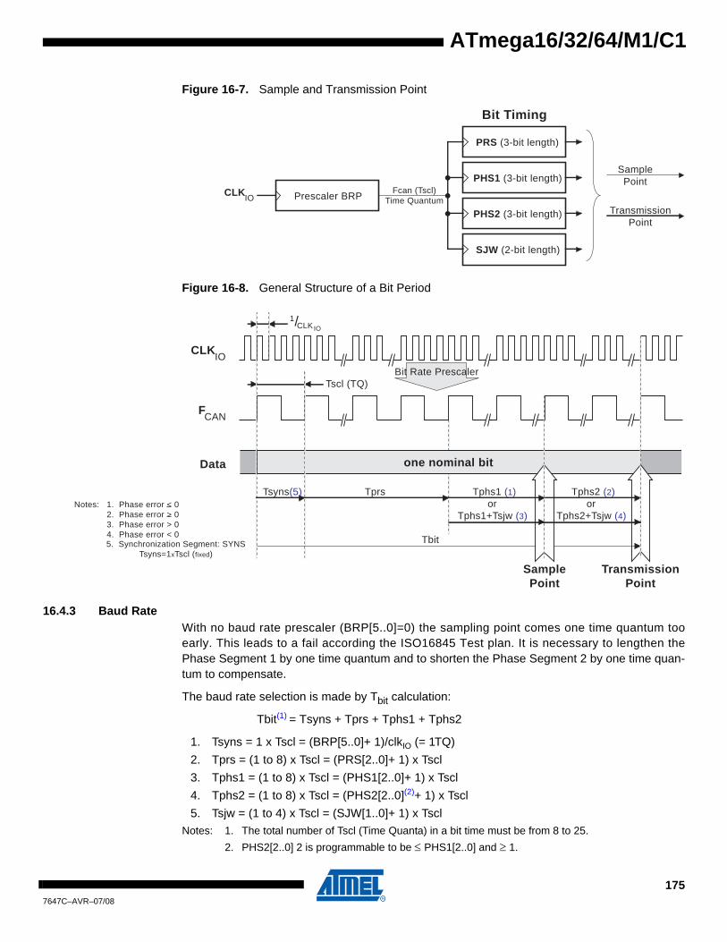
ATmega16/32/64/M1/C1
Figure 16-7. Sample and Transmission Point
Figure 16-8. General Structure of a Bit Period
16.4.3 Baud RateWith no baud rate prescaler (BRP[5..0]=0) the sampling point comes one time quantum tooearly. This leads to a fail according the ISO16845 Test plan. It is necessary to lengthen thePhase Segment 1 by one time quantum and to shorten the Phase Segment 2 by one time quan-tum to compensate.
The baud rate selection is made by Tbit calculation:
Tbit(1) = Tsyns + Tprs + Tphs1 + Tphs2
1. Tsyns = 1 x Tscl = (BRP[5..0]+ 1)/clkIO (= 1TQ) 2. Tprs = (1 to 8) x Tscl = (PRS[2..0]+ 1) x Tscl 3. Tphs1 = (1 to 8) x Tscl = (PHS1[2..0]+ 1) x Tscl 4. Tphs2 = (1 to 8) x Tscl = (PHS2[2..0](2)+ 1) x Tscl 5. Tsjw = (1 to 4) x Tscl = (SJW[1..0]+ 1) x Tscl
Notes: 1. The total number of Tscl (Time Quanta) in a bit time must be from 8 to 25.2. PHS2[2..0] 2 is programmable to be ≤ PHS1[2..0] and ≥ 1.
Bit Timing
SamplePoint
TransmissionPoint
Prescaler BRP
PRS (3-bit length)
SJW (2-bit length)
PHS1 (3-bit length)
PHS2 (3-bit length)
CLKIOFcan (Tscl)
Time Quantum
Bit Rate Prescaler
CLKIO
FCAN
Data
Tscl (TQ)
1/CLKIO
one nominal bit
Tsyns(5)
Tphs2+Tsjw (4)Tphs1+Tsjw (3)
Tbit
Tphs2 (2)Tphs1 (1)Tprs
SamplePoint
TransmissionPoint
5. Synchronization Segment: SYNSTsyns=1xTscl (fixed)
Notes: 1. Phase error < 02. Phase error > 03. Phase error > 04. Phase error < 0
or or
1757647C–AVR–07/08

16.4.4 Fault Confinement(c.f. Section 16.7 “Error Management” on page 180).
16.4.5 Overload FrameAn overload frame is sent by setting an overload request (OVRQ). After the next reception, theCAN channel sends an overload frame in accordance with the CAN specification. A status orflag is set (OVRF) as long as the overload frame is sent.
Figure 16-9. Overload Frame
16.5 Message ObjectsThe MOb is a CAN frame descriptor. It contains all information to handle a CAN frame. Thismeans that a MOb has been outlined to allow to describe a CAN message like an object. The setof MObs is the front end part of the “mailbox” where the messages to send and/or to receive arepre-defined as well as possible to decrease the work load of the software.
The MObs are independent but priority is given to the lower one in case of multi matching. Theoperating modes are:
– Disabled mode – Transmit mode– Receive mode– Automatic reply– Frame buffer receive mode
16.5.1 Number of MObsThis device has 6 MObs, they are numbered from 0 up to 5 (i=5).
16.5.2 Operating ModesThere is no default mode after RESET.Every MOb has its own fields to control the operating mode. Before enabling the CAN periph-eral, each MOb must be configured (ex: disabled mode - CONMOB=00).
Ident "A" Cmd Message Data "A" CRC InterframeA Ident "B"
Overload Frame
Overload FrameRXCDAN
Setting OVRQ bit
OVFG bit
Resetting OVRQ bit
TXCDAN
OVRQ bit
Instructions
Table 16-1. MOb Configuration
MOb Configuration Reply Valid RTR Tag Operating Mode
0 0 x x Disabled
0 1x 0 Tx Data Frame
x 1 Tx Remote Frame
1767647C–AVR–07/08
ATmega16/32/64/M1/C1

ATmega16/32/64/M1/C1
16.5.2.1 DisabledIn this mode, the MOb is “free”.
16.5.2.2 Tx Data & Remote Frame1. Several fields must be initialized before sending:
– Identifier tag (IDT)– Identifier extension (IDE)– Remote transmission request (RTRTAG)– Data length code (DLC)– Reserved bit(s) tag (RBnTAG)– Data bytes of message (MSG)
2. The MOb is ready to send a data or a remote frame when the MOb configuration is set (CONMOB).
3. Then, the CAN channel scans all the MObs in Tx configuration, finds the MOb having the highest priority and tries to send it.
4. When the transmission is completed the TXOK flag is set (interrupt).5. All the parameters and data are available in the MOb until a new initialization.
16.5.2.3 Rx Data & Remote Frame1. Several fields must be initialized before receiving:
– Identifier tag (IDT)– Identifier mask (IDMSK)– Identifier extension (IDE)– Identifier extension mask (IDEMSK)– Remote transmission request (RTRTAG)– Remote transmission request mask (RTRMSK)– Data length code (DLC)– Reserved bit(s) tag (RBnTAG)
2. The MOb is ready to receive a data or a remote frame when the MOb configuration is set (CONMOB).
3. When a frame identifier is received on CAN network, the CAN channel scans all the MObs in receive mode, tries to find the MOb having the highest priority which is matching.
4. On a hit, the IDT, the IDE and the DLC of the matched MOb are updated from the incoming (frame) values.
5. Once the reception is completed, the data bytes of the received message are stored (not for remote frame) in the data buffer of the matched MOb and the RXOK flag is set (interrupt).
6. All the parameters and data are available in the MOb until a new initialization.
1 0
x 0 Rx Data Frame
01
Rx Remote Frame
1 Rx Remote Frame then, Tx Data Frame (reply)
1 1 x x Frame Buffer Receive Mode
Table 16-1. MOb Configuration (Continued)
MOb Configuration Reply Valid RTR Tag Operating Mode
1777647C–AVR–07/08
16.5.2.4 Automatic ReplyA reply (data frame) to a remote frame can be automatically sent after reception of the expectedremote frame.
1. Several fields must be initialized before receiving the remote frame:– Reply valid (RPLV) in a identical flow to the one described in Section 16.5.2.3 “Rx
Data & Remote Frame” on page 177. 2. When a remote frame matches, automatically the RTRTAG and the reply valid bit
(RPLV) are reset. No flag (or interrupt) is set at this time. Since the CAN data buffer has not been used by the incoming remote frame, the MOb is then ready to be in transmit mode without any more setting. The IDT, the IDE, the other tags and the DLC of the received remote frame are used for the reply.
3. When the transmission of the reply is completed the TXOK flag is set (interrupt).4. All the parameters and data are available in the MOb until a new initialization.
16.5.2.5 Frame Buffer Receive ModeThis mode is useful to receive multi frames. The priority between MObs offers a management forthese incoming frames. One set MObs (including non-consecutive MObs) is created when theMObs are set in this mode. Due to the mode setting, only one set is possible. A frame buffercompleted flag (or interrupt) - BXOK - will rise only when all the MObs of the set will havereceived their dedicated CAN frame.
1. MObs in frame buffer receive mode need to be initialized as MObs in standard receive mode.2. The MObs are ready to receive data (or a remote) frames when their respective config-
urations are set (CONMOB).3. When a frame identifier is received on CAN network, the CAN channel scans all the
MObs in receive mode, tries to find the MOb having the highest priority which is matching.
4. On a hit, the IDT, the IDE and the DLC of the matched MOb are updated from the incoming (frame) values.
5. Once the reception is completed, the data bytes of the received message are stored (not for remote frame) in the data buffer of the matched MOb and the RXOK flag is set (interrupt).
6. When the reception in the last MOb of the set is completed, the frame buffer completed BXOK flag is set (interrupt). BXOK flag can be cleared only if all CONMOB fields of the set have been re-written before.
7. All the parameters and data are available in the MObs until a new initialization.
16.5.3 Acceptance FilterUpon a reception hit (i.e., a good comparison between the ID + RTR + RBn + IDE received and anIDT+ RTRTAG + RBnTAG + IDE specified while taking the comparison mask into account) the IDT+ RTRTAG + RBnTAG + IDE received are updated in the MOb (written over the registers).
1787647C–AVR–07/08
ATmega16/32/64/M1/C1

ATmega16/32/64/M1/C1
Figure 16-10. Acceptance Filter Block Diagram
Note: Examples:
Full filtering: to accept only ID = 0x317 in part A.- ID MSK = 111 1111 1111 b- ID TAG = 011 0001 0111 b
Partiel filtering: to accept ID from 0x310 up to 0x317 in part A.- ID MSK = 111 1111 1000 b- ID TAG = 011 0001 0xxx b
No filtering: to accept all ID’s from 0x000 up to 0x7FF in part A.- ID MSK = 000 0000 0000 b- ID TAG = xxx xxxx xxxx b
16.5.4 MOb PageEvery MOb is mapped into a page to save place. The page number is the MOb number. Thispage number is set in CANPAGE register. The other numbers are reserved for factory tests.
CANHPMOB register gives the MOb having the highest priority in CANSIT registers. It is format-ted to provide a direct entry for CANPAGE register. Because CANHPMOB codes CANSITregisters, it will be only updated if the corresponding enable bits (ENRX, ENTX, ENERR) areenabled (c.f. Figure 16-14).
16.5.5 CAN Data BuffersTo preserve register allocation, the CAN data buffer is seen such as a FIFO (with addresspointer accessible) into a MOb selection.This also allows to reduce the risks of un-controlledaccesses.
There is one FIFO per MOb. This FIFO is accessed into a MOb page thanks to the CAN mes-sage register.
The data index (INDX) is the address pointer to the required data byte. The data byte can beread or write. The data index is automatically incremented after every access if the AINC* bit isreset. A roll-over is implemented, after data index=7 it is data index=0.
The first byte of a CAN frame is stored at the data index=0, the second one at the data index=1,...
CANIDM Registers (MOb[i])
IDMSK RTRMSK IDEMSK
CANIDT Registers & CANCDMOB (MOb[i])
ID & RB RTRTAG IDE
internal RxDcan Rx Shift Register (internal)
ID & RB RTR IDE
=Hit MOb[i]
14(33)
13(31) - RB excluded
RB excluded
13(31)14(33)
WriteEnable
13(31)
1
1797647C–AVR–07/08

16.6 CAN TimerA programmable 16-bit timer is used for message stamping and time trigger communication(TTC).
Figure 16-11. CAN Timer Block Diagram
16.6.1 PrescalerAn 8-bit prescaler is initialized by CANTCON register. It receives the clkIO frequency divided by8. It provides clkCANTIM frequency to the CAN Timer if the CAN controller is enabled.
TclkCANTIM = TclkIO x 8 x (CANTCON [7:0] + 1)
16.6.2 16-bit TimerThis timer starts counting from 0x0000 when the CAN controller is enabled (ENFG bit). Whenthe timer rolls over from 0xFFFF to 0x0000, an interrupt is generated (OVRTIM).
16.6.3 Time TriggeringTwo synchronization modes are implemented for TTC (TTC bit):
– synchronization on Start of Frame (SYNCTTC=0),– synchronization on End of Frame (SYNCTTC=1).
In TTC mode, a frame is sent once, even if an error occurs.
16.6.4 Stamping MessageThe capture of the timer value is done in the MOb which receives or sends the frame. All man-aged MOb are stamped, the stamping of a received (sent) frame occurs on RxOk (TXOK).
16.7 Error Management
16.7.1 Fault ConfinementThe CAN channel may be in one of the three following states:
clk IO
clk CANTIM
CANTIM
CANTTCCANSTM[i]
CANTCON
TTC SYNCTTC
"EOF "
"SOF "
OVRTIM
TXOK[i]
RXOK[i]
overrun
ENFG8
1807647C–AVR–07/08
ATmega16/32/64/M1/C1
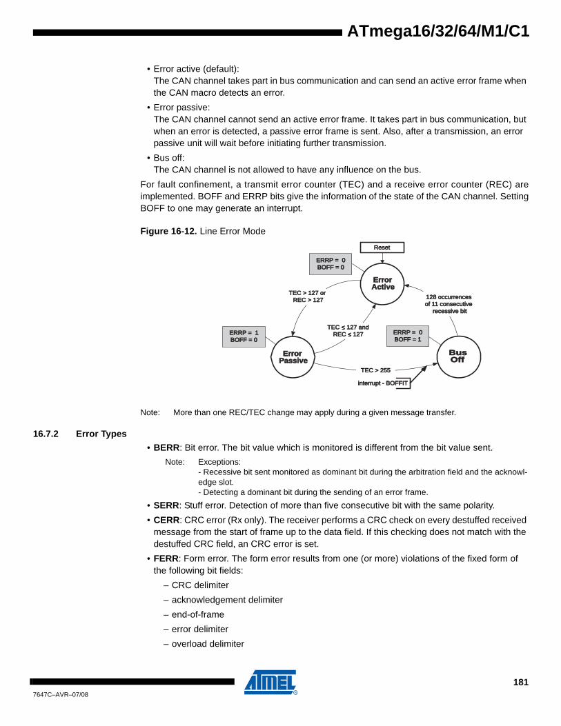
ATmega16/32/64/M1/C1
• Error active (default):The CAN channel takes part in bus communication and can send an active error frame when the CAN macro detects an error.
• Error passive:The CAN channel cannot send an active error frame. It takes part in bus communication, but when an error is detected, a passive error frame is sent. Also, after a transmission, an error passive unit will wait before initiating further transmission.
• Bus off:The CAN channel is not allowed to have any influence on the bus.
For fault confinement, a transmit error counter (TEC) and a receive error counter (REC) areimplemented. BOFF and ERRP bits give the information of the state of the CAN channel. SettingBOFF to one may generate an interrupt.
Figure 16-12. Line Error Mode
Note: More than one REC/TEC change may apply during a given message transfer.
16.7.2 Error Types• BERR: Bit error. The bit value which is monitored is different from the bit value sent.
Note: Exceptions:- Recessive bit sent monitored as dominant bit during the arbitration field and the acknowl-edge slot.- Detecting a dominant bit during the sending of an error frame.
• SERR: Stuff error. Detection of more than five consecutive bit with the same polarity.• CERR: CRC error (Rx only). The receiver performs a CRC check on every destuffed received
message from the start of frame up to the data field. If this checking does not match with the destuffed CRC field, an CRC error is set.
• FERR: Form error. The form error results from one (or more) violations of the fixed form of the following bit fields:
– CRC delimiter– acknowledgement delimiter– end-of-frame– error delimiter– overload delimiter
ERRP = 1BOFF = 0
ErrorActive
ErrorPassive
BusOff
TEC > 127 or REC > 127 128 occurrences
of 11 consecutive recessive bit
Reset
interrupt - BOFFIT
TEC > 255
TEC < 127 and REC < 127
ERRP = 0BOFF = 0
ERRP = 0BOFF = 1
1817647C–AVR–07/08

• AERR: Acknowledgment error (Tx only). No detection of the dominant bit in the acknowledge slot.
Figure 16-13. Error Detection Procedures in a Data Frame
16.7.3 Error SettingThe CAN channel can detect some errors on the CAN network.
• In transmission:The error is set at MOb level.
• In reception:- The identified has matched: The error is set at MOb level.- The identified has not or not yet matched:The error is set at general level.
After detecting an error, the CAN channel sends an error frame on network. If the CAN channeldetects an error frame on network, it sends its own error frame.
16.8 Interrupts
16.8.1 Interrupt organizationThe different interrupts are:
• Interrupt on receive completed OK,• Interrupt on transmit completed OK,• Interrupt on error (bit error, stuff error, CRC error, form error, acknowledge error),• Interrupt on frame buffer full,• Interrupt on “Bus Off” setting,• Interrupt on overrun of CAN timer.
The general interrupt enable is provided by ENIT bit and the specific interrupt enable for CANtimer overrun is provided by ENORVT bit.
Identifier Message DataRTR
ACK error
Form error
Stuff error
Bit error
CRC error
Form error
Stuff error
Bit error
ACK EOFSOF CRCdel.
ACKdel. inter.Control CRC
Tx
Rx
Arbitration
1827647C–AVR–07/08
ATmega16/32/64/M1/C1
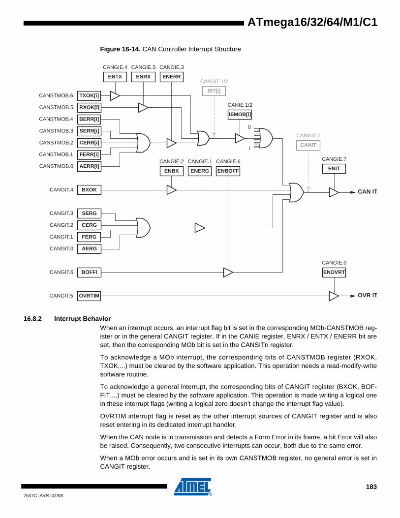
ATmega16/32/64/M1/C1
Figure 16-14. CAN Controller Interrupt Structure
16.8.2 Interrupt BehaviorWhen an interrupt occurs, an interrupt flag bit is set in the corresponding MOb-CANSTMOB reg-ister or in the general CANGIT register. If in the CANIE register, ENRX / ENTX / ENERR bit areset, then the corresponding MOb bit is set in the CANSITn register.
To acknowledge a MOb interrupt, the corresponding bits of CANSTMOB register (RXOK,TXOK,...) must be cleared by the software application. This operation needs a read-modify-writesoftware routine.
To acknowledge a general interrupt, the corresponding bits of CANGIT register (BXOK, BOF-FIT,...) must be cleared by the software application. This operation is made writing a logical onein these interrupt flags (writing a logical zero doesn’t change the interrupt flag value).
OVRTIM interrupt flag is reset as the other interrupt sources of CANGIT register and is alsoreset entering in its dedicated interrupt handler.
When the CAN node is in transmission and detects a Form Error in its frame, a bit Error will alsobe raised. Consequently, two consecutive interrupts can occur, both due to the same error.
When a MOb error occurs and is set in its own CANSTMOB register, no general error is set inCANGIT register.
TXOK[i]CANSTMOB.6
RXOK[i]CANSTMOB.5
BERR[i]CANSTMOB.4
SERR[i]CANSTMOB.3
CERR[i]CANSTMOB.2
FERR[i]CANSTMOB.1
AERR[i]CANSTMOB.0
BXOKCANGIT.4
SERGCANGIT.3
CERGCANGIT.2
FERGCANGIT.1
AERGCANGIT.0
BOFFICANGIT.6
ENTX
CANGIE.4
ENRX
CANGIE.5
ENERR
CANGIE.3
ENBX
CANGIE.2
ENERG
CANGIE.1
ENBOFF
CANGIE.6
IEMOB[i]
CANIE 1/2
ENIT
CANGIE.7
ENOVRT
CANGIE.0
SIT[i]
CANSIT 1/2
CANIT
CANGIT.7
CAN IT
OVR IT
0
i
OVRTIMCANGIT.5
1837647C–AVR–07/08

16.9 CAN Register Description
Figure 16-15. Registers Organization
General ControlGeneral Status
General Interrupt
Bit Timing 1Bit Timing 2Bit Timing 3
Enable MOb 2Enable MOb 1
Enable Interrupt
Status Interrupt MOb 2Status Interrupt MOb 1
Enable Interrupt MOb 2Enable Interrupt MOb 1
CAN Timer Control
CAN TTC LowCAN TTC High
CAN Timer LowCAN Timer High
TEC CounterREC Counter
Hightest Priority MOb
Page MObMOb Number Data Index
ID Tag 2ID Tag 1
ID Tag 4ID Tag 3
ID Mask 2ID Mask 1
ID Mask 4ID Mask 3
Time Stamp LowTime Stamp High
Message Data
MOb StatusMOb Control & DLC
Page MOb
MOb0 - ID Tag 2MOb0 - ID Tag 1
MOb0 - ID Tag 4MOb0 - ID Tag 3
MOb0 - ID Mask 2MOb0 - ID Mask 1
MOb0 - ID Mask 4MOb0 - ID Mask 3
MOb0 - Time Stamp LowMOb0 - Time Stamp High
MOb0 - MOb StatusMOb0 - MOb Ctrl & DLC
MOb0 - Mess. Data - byte 0
MOb(i) - ID Tag 2MOb(i) - ID Tag 1
MOb(i) - ID Tag 4MOb(i) - ID Tag 3
MOb(i) - ID Mask 2MOb(i) - ID Mask 1
MOb(i) - ID Mask 4MOb(i) - ID Mask 3
MOb(i) - Time Stamp LowMOb(i) - Time Stamp High
MOb(i) - MOb StatusMOb(i) - MOb Ctrl & DLC
MOb(i) - Mess. Data - byte 0
(i+1) Message Objects
8 bytes
AVR Registers Registers in Pages
1847647C–AVR–07/08
ATmega16/32/64/M1/C1

ATmega16/32/64/M1/C1
16.10 General CAN Registers
16.10.1 CAN General Control Register - CANGCON
• Bit 7 – ABRQ: Abort RequestThis is not an auto resettable bit.
– 0 - no request.– 1 - abort request: a reset of CANEN1 and CANEN2 registers is done. The pending
communications are immediately disabled and the on-going one will be normally terminated, setting the appropriate status flags. Note that CANCDMOB register remain unchanged.
• Bit 6 – OVRQ: Overload Frame RequestThis is not an auto resettable bit.
– 0 - no request.– 1 - overload frame request: send an overload frame after the next received frame.
The overload frame can be traced observing OVFG in CANGSTA register (c.f. Figure 16-9 onpage 176).
• Bit 5 – TTC: Time Trigger Communication– 0 - no TTC.– 1 - TTC mode.
• Bit 4 – SYNTTC: Synchronization of TTCThis bit is only used in TTC mode.
– 0 - the TTC timer is caught on SOF.– 1 - the TTC timer is caught on the last bit of the EOF.
• Bit 3 – LISTEN: Listening Mode– 0 - no listening mode.– 1 - listening mode.
• Bit 2 – TEST: Test Mode– 0 - no test mode– 1 - test mode: intend for factory testing and not for customer use.
Note: CAN may malfunction if this bit is set.
• Bit 1 – ENA/STB: Enable / Standby ModeBecause this bit is a command and is not immediately effective, the ENFG bit in CANGSTA reg-ister gives the true state of the chosen mode.
Bit 7 6 5 4 3 2 1 0
ABRQ OVRQ TTC SYNTTC LISTEN TEST ENA/STB SWRES CANGCONRead/Write R/W R/W R/W R/W R/W R/W R/W R/W
Initial Value 0 0 0 0 0 0 0 0
1857647C–AVR–07/08

– 0 - standby mode: The on-going transmission (if exists) is normally terminated and the CAN channel is frozen (the CONMOB bits of every MOb do not change). The transmitter constantly provides a recessive level. In this mode, the receiver is not enabled but all the registers and mailbox remain accessible from CPU. In this mode, the receiver is not enabled but all the registers and mailbox remain accessible from CPU.Note:A standby mode applied during a reception may corrupt the on-going reception or set the
controller in a wrong state. The controller will restart correctly from this state if a software reset (SWRES) is applied. If no reset is considered, a possible solution is to wait for a lake of a receiver busy (RXBSY) before to enter in stand-by mode. The best solution is first to apply an abort request command (ABRQ) and then wait for the lake of the receiver busy (RXBSY) before to enter in stand-by mode. In any cases, this standby mode behav-ior has no effect on the CAN bus integrity.
– 1 - enable mode: The CAN channel enters in enable mode once 11 recessive bits has been read.
• Bit 0 – SWRES: Software Reset RequestThis auto resettable bit only resets the CAN controller.
– 0 - no reset– 1 - reset: this reset is “ORed” with the hardware reset.
16.10.2 CAN General Status Register - CANGSTA
• Bit 7 – Reserved BitThis bit is reserved for future use.
• Bit 6 – OVRG: Overload Frame FlagThis flag does not generate an interrupt.
– 0 - no overload frame.– 1 - overload frame: set by hardware as long as the produced overload frame is sent.
• Bit 5 – Reserved BitThis bit is reserved for future use.
• Bit 4 – TXBSY: Transmitter BusyThis flag does not generate an interrupt.
– 0 - transmitter not busy.– 1 - transmitter busy: set by hardware as long as a frame (data, remote, overload or
error frame) or an ACK field is sent. Also set when an inter frame space is sent.
• Bit 3 – RXBSY: Receiver BusyThis flag does not generate an interrupt.
– 0 - receiver not busy– 1 - receiver busy: set by hardware as long as a frame is received or monitored.
Bit 7 6 5 4 3 2 1 0
- OVRG - TXBSY RXBSY ENFG BOFF ERRP CANGSTARead/Write - R - R R R R R
Initial Value - 0 - 0 0 0 0 0
1867647C–AVR–07/08
ATmega16/32/64/M1/C1

ATmega16/32/64/M1/C1
• Bit 2 – ENFG: Enable FlagThis flag does not generate an interrupt.
– 0 - CAN controller disable: because an enable/standby command is not immediately effective, this status gives the true state of the chosen mode.
– 1 - CAN controller enable.
• Bit 1 – BOFF: Bus Off ModeBOFF gives the information of the state of the CAN channel. Only entering in bus off mode gen-erates the BOFFIT interrupt.
– 0 - no bus off mode.– 1 - bus off mode.
• Bit 0 – ERRP: Error Passive ModeERRP gives the information of the state of the CAN channel. This flag does not generate aninterrupt.
– 0 - no error passive mode.– 1 - error passive mode.
16.10.3 CAN General Interrupt Register - CANGIT
• Bit 7 – CANIT: General Interrupt FlagThis is a read only bit.
– 0 - no interrupt.– 1 - CAN interrupt: image of all the CAN controller interrupts except for OVRTIM
interrupt. This bit can be used for polling method.
• Bit 6 – BOFFIT: Bus Off Interrupt FlagWriting a logical one resets this interrupt flag. BOFFIT flag is only set when the CAN enters inbus off mode (coming from error passive mode).
– 0 - no interrupt.– 1 - bus off interrupt when the CAN enters in bus off mode.
• Bit 5 – OVRTIM: Overrun CAN TimerWriting a logical one resets this interrupt flag. Entering in CAN timer overrun interrupt handleralso reset this interrupt flag
– 0 - no interrupt.– 1 - CAN timer overrun interrupt: set when the CAN timer switches from 0xFFFF to 0.
• Bit 4 – BXOK: Frame Buffer Receive InterruptWriting a logical one resets this interrupt flag. BXOK flag can be cleared only if all CONMOBfields of the MOb’s of the buffer have been re-written before.
Bit 7 6 5 4 3 2 1 0
CANIT BOFFIT OVRTIM BXOK SERG CERG FERG AERG CANGITRead/Write R R/W R/W R/W R/W R/W R/W R/W
Initial Value 0 0 0 0 0 0 0 0
1877647C–AVR–07/08

– 0 - no interrupt.– 1 - burst receive interrupt: set when the frame buffer receive is completed.
• Bit 3 – SERG: Stuff Error GeneralWriting a logical one resets this interrupt flag.
– 0 - no interrupt.– 1 - stuff error interrupt: detection of more than 5 consecutive bits with the same
polarity.
• Bit 2 – CERG: CRC Error GeneralWriting a logical one resets this interrupt flag.
– 0 - no interrupt.– 1 - CRC error interrupt: the CRC check on destuffed message does not fit with the
CRC field.
• Bit 1 – FERG: Form Error GeneralWriting a logical one resets this interrupt flag.
– 0 - no interrupt.– 1 - form error interrupt: one or more violations of the fixed form in the CRC delimiter,
acknowledgment delimiter or EOF.
• Bit 0 – AERG: Acknowledgment Error GeneralWriting a logical one resets this interrupt flag.
– 0 - no interrupt.– 1 - acknowledgment error interrupt: no detection of the dominant bit in acknowledge
slot.
16.10.4 CAN General Interrupt Enable Register - CANGIE
• Bit 7 – ENIT: Enable all Interrupts (Except for CAN Timer Overrun Interrupt)– 0 - interrupt disabled.– 1- CANIT interrupt enabled.
• Bit 6 – ENBOFF: Enable Bus Off Interrupt– 0 - interrupt disabled.– 1- bus off interrupt enabled.
• Bit 5 – ENRX: Enable Receive Interrupt– 0 - interrupt disabled.– 1- receive interrupt enabled.
• Bit 4 – ENTX: Enable Transmit Interrupt
Bit 7 6 5 4 3 2 1 0
ENIT ENBOFF ENRX ENTX ENERR ENBX ENERG ENOVRT CANGIERead/Write R/W R/W R/W R/W R/W R/W R/W R/W
Initial Value 0 0 0 0 0 0 0 0
1887647C–AVR–07/08
ATmega16/32/64/M1/C1

ATmega16/32/64/M1/C1
– 0 - interrupt disabled.– 1- transmit interrupt enabled.
• Bit 3 – ENERR: Enable MOb Errors Interrupt– 0 - interrupt disabled.– 1- MOb errors interrupt enabled.
• Bit 2 – ENBX: Enable Frame Buffer Interrupt– 0 - interrupt disabled.– 1- frame buffer interrupt enabled.
• Bit 1 – ENERG: Enable General Errors Interrupt– 0 - interrupt disabled.– 1- general errors interrupt enabled.
• Bit 0 – ENOVRT: Enable CAN Timer Overrun Interrupt– 0 - interrupt disabled.– 1- CAN timer interrupt overrun enabled.
16.10.5 CAN Enable MOb Registers - CANEN2 and CANEN1
• Bits 5:0 - ENMOB5:0: Enable MObThis bit provides the availability of the MOb.It is set to one when the MOb is enabled (i.e. CONMOB1:0 of CANCDMOB register).Once TXOK or RXOK is set to one (TXOK for automatic reply), the corresponding ENMOB isreset. ENMOB is also set to zero configuring the MOb in disabled mode, applying abortion orstandby mode.
– 0 - message object disabled: MOb available for a new transmission or reception.– 1 - message object enabled: MOb in use.
• Bit 15:6 – Reserved BitsThese bits are reserved for future use.
Bit 7 6 5 4 3 2 1 0
- - ENMOB5 ENMOB4 ENMOB3 ENMOB2 ENMOB1 ENMOB0 CANEN2- - - - - - - - CANEN1
Bit 15 14 13 12 11 10 9 8
Read/Write R R R R R R R R
Initial Value 0 0 0 0 0 0 0 0
Read/Write R R R R R R R R
Initial Value 0 0 0 0 0 0 0 0
1897647C–AVR–07/08

16.10.6 CAN Enable Interrupt MOb Registers - CANIE2 and CANIE1
• Bits 5:0 - IEMOB5:0: Interrupt Enable by MOb– 0 - interrupt disabled.– 1 - MOb interrupt enabled
Note: Example: CANIE2 = 0000 1100b : enable of interrupts on MOb 2 & 3.
• Bit 15:6 – Reserved BitsThese bits are reserved for future use. For compatibility with future devices, it must be written tozero when CANIE1 & CANIE2 are written.
16.10.7 CAN Status Interrupt MOb Registers - CANSIT2 and CANSIT1
• Bits 5:0 - SIT5:0: Status of Interrupt by MOb– 0 - no interrupt.– 1- MOb interrupt.
Note: Example: CANSIT2 = 0010 0001b : MOb 0 & 5 interrupts.
• Bit 15:6 – Reserved BitsThese bits are reserved for future use.
16.10.8 CAN Bit Timing Register 1 - CANBT1
• Bit 7– Reserved BitThis bit is reserved for future use. For compatibility with future devices, it must be written to zerowhen CANBT1 is written.
• Bit 6:1 – BRP5:0: Baud Rate Prescaler
Bit 7 6 5 4 3 2 1 0
- - IEMOB5 IEMOB4 IEMOB3 IEMOB2 IEMOB1 IEMOB0 CANIE2- - - - - - - - CANIE1
Bit 15 14 13 12 11 10 9 8
Read/Write R/W R/W R/W R/W R/W R/W R/W R/W
Initial Value 0 0 0 0 0 0 0 0
Read/Write R R/W R/W R/W R/W R/W R/W R/W
Initial Value 0 0 0 0 0 0 0 0
Bit 7 6 5 4 3 2 1 0
- - SIT5 SIT4 SIT3 SIT2 SIT1 SIT0 CANSIT2- - - - - - - - CANSIT1
Bit 15 14 13 12 11 10 9 8
Read/Write R R R R R R R R
Initial Value 0 0 0 0 0 0 0 0
Read/Write R R R R R R R R
Initial Value 0 0 0 0 0 0 0 0
Bit 7 6 5 4 3 2 1 0
- BRP5 BRP4 BRP3 BRP2 BRP1 BRP0 - CANBT1Read/Write - R/W R/W R/W R/W R/W R/W -
Initial Value - 0 0 0 0 0 0 -
1907647C–AVR–07/08
ATmega16/32/64/M1/C1

ATmega16/32/64/M1/C1
The period of the CAN controller system clock Tscl is programmable and determines the individ-ual bit timing.
If ‘BRP[5..0]=0’, see Section 16.4.3 “Baud Rate” on page 175 and Section • “Bit 0 – SMP: Sam-ple Point(s)” on page 192.
• Bit 0 – Reserved BitThis bit is reserved for future use. For compatibility with future devices, it must be written to zerowhen CANBT1 is written.
16.10.9 CAN Bit Timing Register 2 - CANBT2
• Bit 7– Reserved BitThis bit is reserved for future use. For compatibility with future devices, it must be written to zerowhen CANBT2 is written.
• Bit 6:5 – SJW1:0: Re-Synchronization Jump WidthTo compensate for phase shifts between clock oscillators of different bus controllers, the control-ler must re-synchronize on any relevant signal edge of the current transmission.The synchronization jump width defines the maximum number of clock cycles. A bit period maybe shortened or lengthened by a re-synchronization.
• Bit 4 – Reserved BitThis bit is reserved for future use. For compatibility with future devices, it must be written to zerowhen CANBT2 is written.
• Bit 3:1 – PRS2:0: Propagation Time SegmentThis part of the bit time is used to compensate for the physical delay times within the network. Itis twice the sum of the signal propagation time on the bus line, the input comparator delay andthe output driver delay.
• Bit 0 – Reserved BitThis bit is reserved for future use. For compatibility with future devices, it must be written to zerowhen CANBT2 is written.
Tscl =BRP[5:0] + 1clkIO frequency
Bit 7 6 5 4 3 2 1 0
- SJW1 SJW0 - PRS2 PRS1 PRS0 - CANBT2Read/Write - R/W R/W - R/W R/W R/W -
Initial Value - 0 0 - 0 0 0 -
Tsjw = Tscl x (SJW [1:0] +1)
Tprs = Tscl x (PRS [2:0] + 1)
1917647C–AVR–07/08

16.10.10 CAN Bit Timing Register 3 - CANBT3
• Bit 7– Reserved BitThis bit is reserved for future use. For compatibility with future devices, it must be written to zerowhen CANBT3 is written.
• Bit 6:4 – PHS22:0: Phase Segment 2This phase is used to compensate for phase edge errors. This segment may be shortened bythe re-synchronization jump width. PHS2[2..0] shall be ≥1 and ≤PHS1[2..0] (c.f. Section 16.2.3“CAN Bit Timing” on page 169 and Section 16.4.3 “Baud Rate” on page 175).
• Bit 3:1 – PHS12:0: Phase Segment 1This phase is used to compensate for phase edge errors. This segment may be lengthened bythe re-synchronization jump width.
• Bit 0 – SMP: Sample Point(s)This option allows to filter possible noise on TxCAN input pin.
– 0 - the sampling will occur once at the user configured sampling point - SP.– 1 - with three-point sampling configuration the first sampling will occur two TclkIO
clocks before the user configured sampling point - SP, again at one TclkIO clock before SP and finally at SP. Then the bit level will be determined by a majority vote of the three samples.
‘SMP=1’ configuration is not compatible with ‘BRP[5:0]=0’ because TQ = TclkIO.If BRP = 0, SMP must be cleared.
16.10.11 CAN Timer Control Register - CANTCON
• Bit 7:0 – TPRSC7:0: CAN Timer PrescalerPrescaler for the CAN timer upper counter range 0 to 255. It provides the clock to the CAN timerif the CAN controller is enabled.
TclkCANTIM = TclkIO x 8 x (CANTCON [7:0] + 1)
Bit 7 6 5 4 3 2 1 0
- PHS22 PHS21 PHS20 PHS12 PHS11 PHS10 SMP CANBT3Read/Write - R/W R/W R/W R/W R/W R/W R/W
Initial Value - 0 0 0 0 0 0 0
Tphs2 = Tscl x (PHS2 [2:0] + 1)
Tphs1 = Tscl x (PHS1 [2:0] + 1)
Bit 7 6 5 4 3 2 1 0
TPRSC7 TPRSC6 TPRSC5 TPRSC4 TPRSC3 TPRSC2 TRPSC1 TPRSC0 CANTCONRead/Write R/W R/W R/W R/W R/W R/W R/W R/W
Initial Value 0 0 0 0 0 0 0 0
1927647C–AVR–07/08
ATmega16/32/64/M1/C1

ATmega16/32/64/M1/C1
16.10.12 CAN Timer Registers - CANTIML and CANTIMH
• Bits 15:0 - CANTIM15:0: CAN Timer CountCAN timer counter range 0 to 65,535.
16.10.13 CAN TTC Timer Registers - CANTTCL and CANTTCH
• Bits 15:0 - TIMTTC15:0: TTC Timer CountCAN TTC timer counter range 0 to 65,535.
16.10.14 CAN Transmit Error Counter Register - CANTEC
• Bit 7:0 – TEC7:0: Transmit Error CountCAN transmit error counter range 0 to 255.
16.10.15 CAN Receive Error Counter Register - CANREC
• Bit 7:0 – REC7:0: Receive Error CountCAN receive error counter range 0 to 255.
16.10.16 CAN Highest Priority MOb Register - CANHPMOB
• Bit 7:4 – HPMOB3:0: Highest Priority MOb NumberMOb having the highest priority in CANSIT registers.If CANSIT = 0 (no MOb), the return value is 0xF.
Note: Do not confuse “MOb priority” and “Message ID priority”- See “Message Objects” on page 176.
Bit 7 6 5 4 3 2 1 0
CANTIM7 CANTIM6 CANTIM5 CANTIM4 CANTIM3 CANTIM2 CANTIM1 CANTIM0 CANTIMLCANTIM15 CANTIM14 CANTIM13 CANTIM12 CANTIM11 CANTIM10 CANTIM9 CANTIM8 CANTIMH
Bit 15 14 13 12 11 10 9 8
Read/Write R R R R R R R R
Initial Value 0 0 0 0 0 0 0 0
Bit 7 6 5 4 3 2 1 0
TIMTTC7 TIMTTC6 TIMTTC5 TIMTTC4 TIMTTC3 TIMTTC2 TIMTTC1 TIMTTC0 CANTTCLTIMTTC15 TIMTTC14 TIMTTC13 TIMTTC12 TIMTTC11 TIMTTC10 TIMTTC9 TIMTTC8 CANTTCH
Bit 15 14 13 12 11 10 9 8
Read/Write R R R R R R R R
Initial Value 0 0 0 0 0 0 0 0
Bit 7 6 5 4 3 2 1 0
TEC7 TEC6 TEC5 TEC4 TEC3 TEC2 TEC1 TEC0 CANTECRead/Write R R R R R R R R
Initial Value 0 0 0 0 0 0 0 0
Bit 7 6 5 4 3 2 1 0
REC7 REC6 REC5 REC4 REC3 REC2 REC1 REC0 CANRECRead/Write R R R R R R R R
Initial Value 0 0 0 0 0 0 0 0
Bit 7 6 5 4 3 2 1 0
HPMOB3 HPMOB2 HPMOB1 HPMOB0 CGP3 CGP2 CGP1 CGP0 CANHPMOBRead/Write R R R R R/W R/W R/W R/W
Initial Value 1 1 1 1 0 0 0 0
1937647C–AVR–07/08

• Bit 3:0 – CGP3:0: CAN General Purpose BitsThese bits can be pre-programmed to match with the wanted configuration of the CANPAGEregister (i.e., AINC and INDX2:0 setting).
16.10.17 CAN Page MOb Register - CANPAGE
• Bit 7:4 – MOBNB3:0: MOb NumberSelection of the MOb number, the available numbers are from 0 to 5.
Note: MOBNB3 always must be written to zero for compatibility with all AVR CAN devices.
• Bit 3 – AINC: Auto Increment of the FIFO CAN Data Buffer Index (Active Low)– 0 - auto increment of the index (default value).– 1- no auto increment of the index.
• Bit 2:0 – INDX2:0: FIFO CAN Data Buffer IndexByte location of the CAN data byte into the FIFO for the defined MOb.
16.11 MOb RegistersThe MOb registers has no initial (default) value after RESET.
16.11.1 CAN MOb Status Register - CANSTMOB
• Bit 7 – DLCW: Data Length Code WarningThe incoming message does not have the DLC expected. Whatever the frame type, the DLCfield of the CANCDMOB register is updated by the received DLC.
• Bit 6 – TXOK: Transmit OKThis flag can generate an interrupt. It must be cleared using a read-modify-write software routineon the whole CANSTMOB register.
The communication enabled by transmission is completed. TxOK rises at the end of EOF field.When the controller is ready to send a frame, if two or more message objects are enabled asproducers, the lower MOb index (0 to 14) is supplied first.
• Bit 5 – RXOK: Receive OKThis flag can generate an interrupt. It must be cleared using a read-modify-write software routineon the whole CANSTMOB register.
The communication enabled by reception is completed. RxOK rises at the end of the 6th bit ofEOF field. In case of two or more message object reception hits, the lower MOb index (0 to 14)is updated first.
Bit 7 6 5 4 3 2 1 0
MOBNB3 MOBNB2 MOBNB1 MOBNB0 AINC INDX2 INDX1 INDX0 CANPAGERead/Write R/W R/W R/W R/W R/W R/W R/W R/W
Initial Value 0 0 0 0 0 0 0 0
Bit 7 6 5 4 3 2 1 0
DLCW TXOK RXOK BERR SERR CERR FERR AERR CANSTMOBRead/Write R/W R/W R/W R/W R/W R/W R/W R/W
Initial Value - - - - - - - -
1947647C–AVR–07/08
ATmega16/32/64/M1/C1

ATmega16/32/64/M1/C1
• Bit 4 – BERR: Bit Error (Only in Transmission)This flag can generate an interrupt. It must be cleared using a read-modify-write software routineon the whole CANSTMOB register.
The bit value monitored is different from the bit value sent.
Exceptions: the monitored recessive bit sent as a dominant bit during the arbitration field and theacknowledge slot detecting a dominant bit during the sending of an error frame.
• Bit 3 – SERR: Stuff ErrorThis flag can generate an interrupt. It must be cleared using a read-modify-write software routineon the whole CANSTMOB register.
Detection of more than five consecutive bits with the same polarity. This flag can generate aninterrupt.
• Bit 2 – CERR: CRC ErrorThis flag can generate an interrupt. It must be cleared using a read-modify-write software routineon the whole CANSTMOB register.
The receiver performs a CRC check on every de-stuffed received message from the start offrame up to the data field. If this checking does not match with the de-stuffed CRC field, a CRCerror is set.
• Bit 1 – FERR: Form ErrorThis flag can generate an interrupt. It must be cleared using a read-modify-write software routineon the whole CANSTMOB register.
The form error results from one or more violations of the fixed form in the following bit fields:
• CRC delimiter.• Acknowledgment delimiter.• EOF
• Bit 0 – AERR: Acknowledgment ErrorThis flag can generate an interrupt. It must be cleared using a read-modify-write software routineon the whole CANSTMOB register.
No detection of the dominant bit in the acknowledge slot.
16.11.2 CAN MOb Control and DLC Register - CANCDMOB
• Bit 7:6 – CONMOB1:0: Configuration of Message ObjectThese bits set the communication to be performed (no initial value after RESET).
– 00 - disable.– 01 - enable transmission.– 10 - enable reception.– 11 - enable frame buffer reception
Bit 7 6 5 4 3 2 1 0
CONMOB1 CONMOB0 RPLV IDE DLC3 DLC2 DLC1 DLC0 CANCDMOBRead/Write R/W R/W R/W R/W R/W R/W R/W R/W
Initial Value - - - - - - - -
1957647C–AVR–07/08

These bits are not cleared once the communication is performed. The user must re-write theconfiguration to enable a new communication.
• This operation is necessary to be able to reset the BXOK flag.• This operation also set the corresponding bit in the CANEN registers.
• Bit 5 – RPLV: Reply ValidUsed in the automatic reply mode after receiving a remote frame.
– 0 - reply not ready.– 1 - reply ready and valid.
• Bit 4 – IDE: Identifier ExtensionIDE bit of the remote or data frame to send.This bit is updated with the corresponding value of the remote or data frame received.
– 0 - CAN standard rev 2.0 A (identifiers length = 11 bits).– 1 - CAN standard rev 2.0 B (identifiers length = 29 bits).
• Bit 3:0 – DLC3:0: Data Length CodeNumber of Bytes in the data field of the message.
DLC field of the remote or data frame to send. The range of DLC is from 0 up to 8. If DLC field >8then effective DLC=8.
This field is updated with the corresponding value of the remote or data frame received. If theexpected DLC differs from the incoming DLC, a DLC warning appears in the CANSTMOBregister.
16.11.3 CAN Identifier Tag Registers - CANIDT1, CANIDT2, CANIDT3, and CANIDT4
V2.0 part A
V2.0 part B
Bit 15/7 14/6 13/5 12/4 11/3 10/2 9/1 8/0
- - - - - RTRTAG - RB0TAG CANIDT4- - - - - - - - CANIDT3
IDT2 IDT1 IDT0 - - - - - CANIDT2IDT10 IDT9 IDT8 IDT7 IDT6 IDT5 IDT4 IDT3 CANIDT1
Bit 31/23 30/22 29/21 28/20 27/19 26/18 25/17 24/16
Read/Write R/W R/W R/W R/W R/W R/W R/W R/W
Initial Value - - - - - - - -
Bit 15/7 14/6 13/5 12/4 11/3 10/2 9/1 8/0
IDT4 IDT3 IDT2 IDT1 IDT0 RTRTAG RB1TAG RB0TAG CANIDT4IDT12 IDT11 IDT10 IDT9 IDT8 IDT7 IDT6 IDT5 CANIDT3IDT20 IDT19 IDT18 IDT17 IDT16 IDT15 IDT14 IDT13 CANIDT2IDT28 IDT27 IDT26 IDT25 IDT24 IDT23 IDT22 IDT21 CANIDT1
Bit 31/23 30/22 29/21 28/20 27/19 26/18 25/17 24/16
Read/Write R/W R/W R/W R/W R/W R/W R/W R/W
Initial Value - - - - - - - -
1967647C–AVR–07/08
ATmega16/32/64/M1/C1

ATmega16/32/64/M1/C1
V2.0 part A
• Bit 31:21 – IDT10:0: Identifier TagIdentifier field of the remote or data frame to send.
This field is updated with the corresponding value of the remote or data frame received.
• Bit 20:3 – Reserved BitsThese bits are reserved for future use. For compatibility with future devices, they must be writtento zero when CANIDTn are written.
When a remote or data frame is received, these bits do not operate in the comparison but theyare updated with un-predicted values.
• Bit 2 – RTRTAG: Remote Transmission Request TagRTR bit of the remote or data frame to send.
This tag is updated with the corresponding value of the remote or data frame received. In caseof Automatic Reply mode, this bit is automatically reset before sending the response.
• Bit 1 – Reserved BitThis bit is reserved for future use. For compatibility with future devices, it must be written to zerowhen CANIDTn are written.
When a remote or data frame is received, this bit does not operate in the comparison but it isupdated with un-predicted values.
• Bit 0 – RB0TAG: Reserved Bit 0 TagRB0 bit of the remote or data frame to send.
This tag is updated with the corresponding value of the remote or data frame received.
V2.0 part B
• Bit 31:3 – IDT28:0: Identifier TagIdentifier field of the remote or data frame to send.
This field is updated with the corresponding value of the remote or data frame received.
• Bit 2 – RTRTAG: Remote Transmission Request TagRTR bit of the remote or data frame to send.
This tag is updated with the corresponding value of the remote or data frame received. In caseof Automatic Reply mode, this bit is automatically reset before sending the response.
• Bit 1 – RB1TAG: Reserved Bit 1 TagRB1 bit of the remote or data frame to send.
This tag is updated with the corresponding value of the remote or data frame received.
• Bit 0 – RB0TAG: Reserved Bit 0 TagRB0 bit of the remote or data frame to send.
This tag is updated with the corresponding value of the remote or data frame received.
1977647C–AVR–07/08
16.11.4 CAN Identifier Mask Registers - CANIDM1, CANIDM2, CANIDM3, and CANIDM4
V2.0 part A
V2.0 part B
V2.0 part A
• Bit 31:21 – IDMSK10:0: Identifier Mask– 0 - comparison true forced - See “Acceptance Filter” on page 178.– 1 - bit comparison enabled - See “Acceptance Filter” on page 178.
• Bit 20:3 – Reserved BitsThese bits are reserved for future use. For compatibility with future devices, they must be writtento zero when CANIDMn are written.
• Bit 2 – RTRMSK: Remote Transmission Request Mask– 0 - comparison true forced– 1 - bit comparison enabled.
• Bit 1 – Reserved BitThis bit is reserved for future use. For compatibility with future devices, it must be written to zerowhen CANIDTn are written.
• Bit 0 – IDEMSK: Identifier Extension Mask– 0 - comparison true forced– 1 - bit comparison enabled.
V2.0 part B
• Bit 31:3 – IDMSK28:0: Identifier Mask– 0 - comparison true forced - See “Acceptance Filter” on page 178.– 1 - bit comparison enabled. - See “Acceptance Filter” on page 178.
• Bit 2 – RTRMSK: Remote Transmission Request Mask
Bit 15/7 14/6 13/5 12/4 11/3 10/2 9/1 8/0
- - - - - RTRMSK - IDEMSK CANIDM4- - - - - - - - CANIDM3
IDMSK2 IDMSK1 IDMSK0 - - - - - CANIDM2IDMSK10 IDMSK9 IDMSK8 IDMSK7 IDMSK6 IDMSK5 IDMSK4 IDMSK3 CANIDM1
Bit 31/23 30/22 29/21 28/20 27/19 26/18 25/17 24/16
Read/Write R/W R/W R/W R/W R/W R/W R/W R/W
Initial Value - - - - - - - -
Bit 15/7 14/6 13/5 12/4 11/3 10/2 9/1 8/0
IDMSK4 IDMSK3 IDMSK2 IDMSK1 IDMSK0 RTRMSK - IDEMSK CANIDM4IDMSK12 IDMSK11 IDMSK10 IDMSK9 IDMSK8 IDMSK7 IDMSK6 IDMSK5 CANIDM3IDMSK20 IDMSK19 IDMSK18 IDMSK17 IDMSK16 IDMSK15 IDMSK14 IDMSK13 CANIDM2IDMSK28 IDMSK27 IDMSK26 IDMSK25 IDMSK24 IDMSK23 IDMSK22 IDMSK21 CANIDM1
Bit 31/23 30/22 29/21 28/20 27/19 26/18 25/17 24/16
Read/Write R/W R/W R/W R/W R/W R/W R/W R/W
Initial Value - - - - - - - -
1987647C–AVR–07/08
ATmega16/32/64/M1/C1
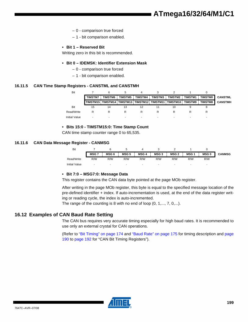
ATmega16/32/64/M1/C1
– 0 - comparison true forced– 1 - bit comparison enabled.
• Bit 1 – Reserved BitWriting zero in this bit is recommended.
• Bit 0 – IDEMSK: Identifier Extension Mask– 0 - comparison true forced– 1 - bit comparison enabled.
16.11.5 CAN Time Stamp Registers - CANSTML and CANSTMH
• Bits 15:0 - TIMSTM15:0: Time Stamp CountCAN time stamp counter range 0 to 65,535.
16.11.6 CAN Data Message Register - CANMSG
• Bit 7:0 – MSG7:0: Message DataThis register contains the CAN data byte pointed at the page MOb register.
After writing in the page MOb register, this byte is equal to the specified message location of thepre-defined identifier + index. If auto-incrementation is used, at the end of the data register writ-ing or reading cycle, the index is auto-incremented.The range of the counting is 8 with no end of loop (0, 1,..., 7, 0,...).
16.12 Examples of CAN Baud Rate SettingThe CAN bus requires very accurate timing especially for high baud rates. It is recommended touse only an external crystal for CAN operations.
(Refer to “Bit Timing” on page 174 and “Baud Rate” on page 175 for timing description and page190 to page 192 for “CAN Bit Timing Registers”).
Bit 7 6 5 4 3 2 1 0
TIMSTM7 TIMSTM6 TIMSTM5 TIMSTM4 TIMSTM3 TIMSTM2 TIMSTM1 TIMSTM0 CANSTMLTIMSTM15 TIMSTM14 TIMSTM13 TIMSTM12 TIMSTM11 TIMSTM10 TIMSTM9 TIMSTM8 CANSTMH
Bit 15 14 13 12 11 10 9 8
Read/Write R R R R R R R R
Initial Value - - - - - - - -
Bit 7 6 5 4 3 2 1 0
MSG 7 MSG 6 MSG 5 MSG 4 MSG 3 MSG 2 MSG 1 MSG 0 CANMSGRead/Write R/W R/W R/W R/W R/W R/W R/W R/W
Initial Value - - - - - - - -
1997647C–AVR–07/08

Table 16-2. Examples of CAN Baud Rate Settings for Commonly Frequencies
fCLKIO(MHz)
CANRate
(Kbps)
Description Segments Registers
SamplingPoint
TQ(µs)
Tbit(TQ)
Tprs(TQ)
Tph1(TQ)
Tph2(TQ)
Tsjw(TQ) CANBT1 CANBT2 CANBT3
16.000
100069 % (1) 0.0625 16 7 4 4 1 0x00 0x0C 0x36 (2)
75 % 0.125 8 3 2 2 1 0x02 0x04 0x13
500 75 %0.125 16 7 4 4 1 0x02 0x0C 0x37
0.250 8 3 2 2 1 0x06 0x04 0x13
250 75 %0.250 16 7 4 4 1 0x06 0x0C 0x37
0.500 8 3 2 2 1 0x0E 0x04 0x13
200 75 %0.3125 16 7 4 4 1 0x08 0x0C 0x37
0.625 8 3 2 2 1 0x12 0x04 0x13
125 75 %0.500 16 7 4 4 1 0x0E 0x0C 0x37
1.000 8 3 2 2 1 0x1E 0x04 0x13
100 75 %0.625 16 7 4 4 1 0x12 0x0C 0x37
1.250 8 3 2 2 1 0x26 0x04 0x13
12.000
1000 67 % (1)0.083333 12 5 3 3 1 0x00 0x08 0x24 (2)
x - - - n o d a t a - - -
500 75 %0.166666 12 5 3 3 1 0x02 0x08 0x25
0.250 8 3 2 2 1 0x04 0x04 0x13
250 75 %0.250 16 7 4 4 1 0x04 0x0C 0x37
0.500 8 3 2 2 1 0x0A 0x04 0x13
200 75 %0.250 20 8 6 5 1 0x04 0x0E 0x4B
0.416666 12 5 3 3 1 0x08 0x08 0x25
125 75 %0.500 16 7 4 4 1 0x0A 0x0C 0x37
1.000 8 3 2 2 1 0x16 0x04 0x13
100 75 %0.500 20 8 6 5 1 0x0A 0x0E 0x4B
0.833333 12 5 3 3 1 0x12 0x08 0x25
2007647C–AVR–07/08
ATmega16/32/64/M1/C1

ATmega16/32/64/M1/C1
Note: 1. See Section 16.4.3 “Baud Rate” on page 175.2. See Section • “Bit 0 – SMP: Sample Point(s)” on page 192
8.000
1000 63 % (1)x - - - n o d a t a - - -
0.125 8 3 2 2 1 0x00 0x04 0x12 (2)
50069 % (1) 0.125 16 7 4 4 1 0x00 0x0C 0x36 (2)
75 % 0.250 8 3 2 2 1 0x02 0x04 0x13
250 75 %0.250 16 7 4 4 1 0x02 0x0C 0x37
0.500 8 3 2 2 1 0x06 0x04 0x13
200 75 %0.250 20 8 6 5 1 0x02 0x0E 0x4B
0.625 8 3 2 2 1 0x08 0x04 0x13
125 75 %0.500 16 7 4 4 1 0x06 0x0C 0x37
1.000 8 3 2 2 1 0x0E 0x04 0x13
100 75 %0.625 16 7 4 4 1 0x08 0x0C 0x37
1.250 8 3 2 2 1 0x12 0x04 0x13
6.000
1000 - - - n o t a p p l i c a b l e - - -
500 67 % (1)0.166666 12 5 3 3 1 0x00 0x08 0x24 (2)
x - - - n o d a t a - - -
250 75 %0.333333 12 5 3 3 1 0x02 0x08 0x25
0.500 8 3 2 2 1 0x04 0x04 0x13
200 80 %0.333333 15 7 4 3 1 0x02 0x0C 0x35
0.500 10 4 3 2 1 0x04 0x06 0x23
125 75 %0.500 16 7 4 4 1 0x04 0x0C 0x37
1.000 8 3 2 2 1 0x0A 0x04 0x13
100 75 %0.500 20 8 6 5 1 0x04 0x0E 0x4B
0.833333 12 5 3 3 1 0x08 0x08 0x25
4.000
1000 - - - n o t a p p l i c a b l e - - -
500 63 % (1)x - - - n o d a t a - - -
0.250 8 3 2 2 1 0x00 0x04 0x12 (2)
25069 % (1) 0.250 16 7 4 4 1 0x00 0x0C 0x36 (2)
75 % 0.500 8 3 2 2 1 0x02 0x04 0x13
200 70 % (1)0.250 20 8 6 5 1 0x00 0x0E 0x4A (2)
x - - - n o d a t a - - -
125 75 %0.500 16 7 4 4 1 0x02 0x0C 0x37
1.000 8 3 2 2 1 0x06 0x04 0x13
100 75 %0.500 20 8 6 5 1 0x02 0x0E 0x4B
1.250 8 3 2 2 1 0x08 0x04 0x13
Table 16-2. Examples of CAN Baud Rate Settings for Commonly Frequencies (Continued)
fCLKIO(MHz)
CANRate
(Kbps)
Description Segments Registers
SamplingPoint
TQ(µs)
Tbit(TQ)
Tprs(TQ)
Tph1(TQ)
Tph2(TQ)
Tsjw(TQ) CANBT1 CANBT2 CANBT3
2017647C–AVR–07/08

17. LIN / UART - Local Interconnect Network Controller or UARTThe LIN (Local Interconnect Network) is a serial communications protocol which efficiently sup-ports the control of mechatronics nodes in distributed automotive applications. The mainproperties of the LIN bus are:
• Single master with multiple slaves concept• Low cost silicon implementation based on common UART/SCI interface• Self synchronization in slave node• Deterministic signal transmission with signal propagation time computable in advance• Low cost single-wire implementation• Speed up to 20 Kbit/s.
LIN provides a cost efficient bus communication where the bandwidth and versatility of CAN arenot required. The specification of the line driver/receiver needs to match the ISO9141 NRZ-standard.
If LIN is not required, the controller alternatively can be programmed as Universal Asynchronousserial Receiver and Transmitter (UART).
17.1 LIN Features• Hardware Implementation of LIN 2.1 (LIN 1.3 Compatibility)• Small, CPU Efficient and Independent Master/Slave Routines Based on “LIN Work Flow Concept”
of LIN 2.1 Specification • Automatic LIN Header Handling and Filtering of Irrelevant LIN Frames• Automatic LIN Response Handling• Extended LIN Error Detection and Signaling• Hardware Frame Time-out Detection• “Break-in-data” Support Capability• Automatic Re-synchronization to Ensure Proper Frame Integrity• Fully Flexible Extended Frames Support Capabilities
17.2 UART Features• Full Duplex Operation (Independent Serial Receive and Transmit Processes)• Asynchronous Operation• High Resolution Baud Rate Generator• Hardware Support of 8 Data Bits, Odd/Even/No Parity Bit, 1 Stop Bit Frames• Data Over-Run and Framing Error Detection
2027647C–AVR–07/08
ATmega16/32/64/M1/C1
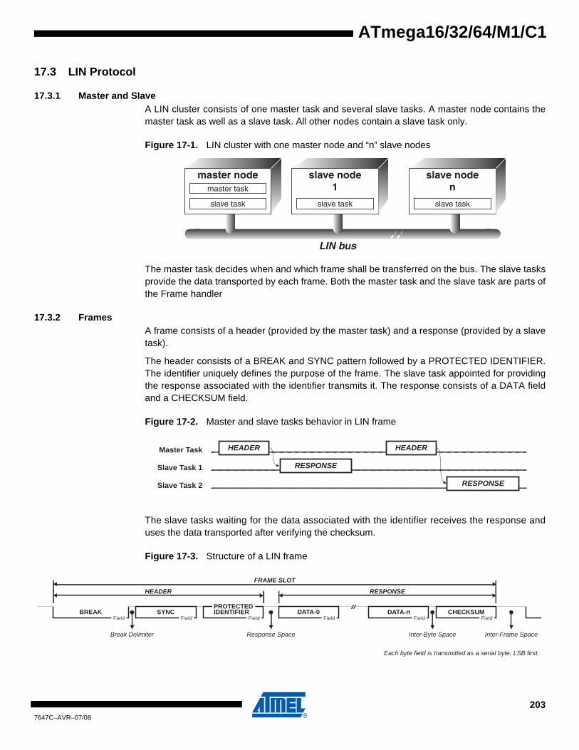
ATmega16/32/64/M1/C1
17.3 LIN Protocol
17.3.1 Master and SlaveA LIN cluster consists of one master task and several slave tasks. A master node contains themaster task as well as a slave task. All other nodes contain a slave task only.
Figure 17-1. LIN cluster with one master node and “n” slave nodes
The master task decides when and which frame shall be transferred on the bus. The slave tasksprovide the data transported by each frame. Both the master task and the slave task are parts ofthe Frame handler
17.3.2 FramesA frame consists of a header (provided by the master task) and a response (provided by a slavetask).
The header consists of a BREAK and SYNC pattern followed by a PROTECTED IDENTIFIER.The identifier uniquely defines the purpose of the frame. The slave task appointed for providingthe response associated with the identifier transmits it. The response consists of a DATA fieldand a CHECKSUM field.
Figure 17-2. Master and slave tasks behavior in LIN frame
The slave tasks waiting for the data associated with the identifier receives the response anduses the data transported after verifying the checksum.
Figure 17-3. Structure of a LIN frame
master task
slave task
master node
slave task
slave node1
slave task
slave noden
LIN bus
Master Task
Slave Task 1
Slave Task 2
HEADER
RESPONSE
HEADER
RESPONSE
BREAKField
SYNCField
CHECKSUMField
DATA-0FieldField
IDENTIFIERPROTECTED
DATA-nField
Break Delimiter Response Space Inter-Byte Space Inter-Frame Space
RESPONSEHEADER
FRAME SLOT
Each byte field is transmitted as a serial byte, LSB first.
2037647C–AVR–07/08

17.3.3 Data TransportTwo types of data may be transported in a frame; signals or diagnostic messages.
• SignalsSignals are scalar values or byte arrays that are packed into the data field of a frame. A sig-nal is always present at the same position in the data field for all frames with the same iden-tifier.
• Diagnostic messagesDiagnostic messages are transported in frames with two reserved identifiers. The interpreta-tion of the data field depends on the data field itself as well as the state of the communicat-ing nodes.
17.3.4 Schedule TableThe master task (in the master node) transmits frame headers based on a schedule table. Theschedule table specifies the identifiers for each header and the interval between the start of aframe and the start of the following frame. The master application may use different scheduletables and select among them.
17.3.5 Compatibility with LIN 1.3LIN 2.1 is a super-set of LIN 1.3.
A LIN 2.1 master node can handle clusters consisting of both LIN 1.3 slaves and/or LIN 2.1slaves. The master will then avoid requesting the new LIN 2.1 features from a LIN 1.3 slave:
• Enhanced checksum,• Re-configuration and diagnostics,• Automatic baud rate detection,• "Response error" status monitoring.LIN 2.1 slave nodes can not operate with a LIN 1.3 master node (e.g. the LIN1.3 master doesnot support the enhanced checksum).
The LIN 2.1 physical layer is backwards compatible with the LIN1.3 physical layer. But not theother way around. The LIN 2.1 physical layer sets greater requirements, i.e. a master nodeusing the LIN 2.1 physical layer can operate in a LIN 1.3 cluster.
17.4 LIN / UART ControllerThe LIN/UART controller is divided in three main functions:• Tx LIN Header function,• Rx LIN Header function,• LIN Response function.
These functions mainly use two services:• Rx service,• Tx service.Because these two services are basically UART services, the controller is also able to switchinto an UART function.
17.4.1 LIN OverviewThe LIN/UART controller is designed to match as closely as possible to the LIN software appli-cation structure. The LIN software application is developed as independent tasks, several slavetasks and one master task (c.f. Section 17.3.4 on page 204). The ATmega16/32/64/M1/C1 con-
2047647C–AVR–07/08
ATmega16/32/64/M1/C1

ATmega16/32/64/M1/C1
forms to this perspective. The only link between the master task and the slave task will be at thecross-over point where the interrupt routine is called once a new identifier is available. Thus, in amaster node, housing both master and slave task, the Tx LIN Header function will alert the slavetask of an identifier presence. In the same way, in a slave node, the Rx LIN Header function willalert the slave task of an identifier presence.
When the slave task is warned of an identifier presence, it has first to analyze it to know what todo with the response. Hardware flags identify the presence of one of the specific identifiers from60 (0x3C) up to 63 (0x3F).
For LIN communication, only four interrupts need to be managed: • LIDOK: New LIN identifier available,• LRXOK: LIN response received,• LTXOK: LIN response transmitted,• LERR: LIN Error(s).The wake-up management can be automated using the UART wake-up capability and a nodesending a minimum of 5 low bits (0xF0) for LIN 2.1 and 8 low bits (0x80) for LIN 1.3. Pin changeinterrupt on LIN wake-up signal can be also used to exit the device of one of its sleep modes.
Extended frame identifiers 62 (0x3E) and 63 (0x3F) are reserved to allow the embedding ofuser-defined message formats and future LIN formats. The byte transfer mode offered by theUART will ensure the upwards compatibility of LIN slaves with accommodation of the LINprotocol.
17.4.2 UART OverviewThe LIN/UART controller can also function as a conventional UART. By default, the UART oper-ates as a full duplex controller. It has local loop back circuitry for test purposes. The UART hasthe ability to buffer one character for transmit and two for receive. The receive buffer is made ofone 8-bit serial register followed by one 8-bit independent buffer register. Automatic flag man-agement is implemented when the application puts or gets characters, thus reducing thesoftware overhead. Because transmit and receive services are independent, the user can saveone device pin when one of the two services is not used. The UART has an enhanced baud rategenerator providing a maximum error of 2% whatever the clock frequency and the targeted baudrate.
2057647C–AVR–07/08

17.4.3 LIN/UART Controller Structure
Figure 17-4. LIN/UART Controller Block Diagram
17.4.4 LIN/UART Command Overview
Figure 17-5. LIN/UART Command Dependencies
BUFFER
FSM
RX Get Byte
Frame Time-out
Synchronization
Monitoring
RxDTX
Put Byte
Finite State Machine
TxD
BAUD_RATE Prescaler Sample /bit
CLK IO
Data FIFO
IDOK
RXOK
RecommendedWay
TXOK
Tx�Response
Tx Header
Rx Headeror
LIN Abort
ByteTransfer
RxByte
TxByte
Rx�Response
LIN
UART
FullDuplex
DISABLE
AutomaticReturn
PossibleWay
2067647C–AVR–07/08
ATmega16/32/64/M1/C1
ATmega16/32/64/M1/C1
17.4.5 Enable / DisableSetting the LENA bit in LINCR register enables the LIN/UART controller. To disable theLIN/UART controller, LENA bit must be written to 0. No wait states are implemented, so, the dis-able command is taken into account immediately.
17.4.6 LIN CommandsClearing the LCMD[2] bit in LINCR register enables LIN commands.
As shown in Table 17-1 on page 207, four functions controlled by the LCMD[1..0] bits of LINCRregister are available (c.f. Figure 17-5 on page 206).
17.4.6.1 Rx Header / LIN Abort FunctionThis function (or state) is mainly the withdrawal mode of the controller.
When the controller has to execute a master task, this state is the start point before enabling aTx Header command.
When the controller has only to execute slave tasks, LIN header detection/acquisition is enabledas background function. At the end of such an acquisition (Rx Header function), automaticallythe appropriate flags are set, and in LIN 1.3, the LINDLR register is set with the uncoded lengthvalue.
This state is also the start point before enabling the Tx or the Rx Response command.
A running function (i.e. Tx Header, Tx or Rx Response) can be aborted by clearing LCMD[1..0]bits in LINCR register. In this case, an abort flag - LABORT - in LINERR register will be set toinform the other software tasks. No wait states are implemented, so, the abort command is takeninto account immediately.
Rx Header function is responsible for:• The BREAK field detection,• The hardware re-synchronization analyzing the SYNCH field,• The reception of the PROTECTED IDENTIFIER field, the parity control and the update of
the LINDLR register in case of LIN 1.3,• The starting of the Frame_Time_Out,• The checking of the LIN communication integrity.
Table 17-1. LIN/UART Command List
LENA LCMD[2] LCMD[1] LCMD[0] Command Comment
0 x x x Disable peripheral
1
0
00 Rx Header - LIN abort LIN withdrawal
1 Tx Header LCMD[2..0]=000 after Tx
10 Rx Response LCMD[2..0]=000 after Rx
1 Tx Response LCMD[2..0]=000 after Tx
1
0 0 Byte transferno CRC, no Time out
LTXDL=LRXDL=0(LINDLR: read only register)
1 0 Rx Byte
0 1 Tx Byte
1 1 Full duplex
2077647C–AVR–07/08

17.4.6.2 Tx Header FunctionIn accordance with the LIN protocol, only the master task must enable this function. The headeris sent in the appropriate timed slots at the programmed baud rate (c.f. LINBRR & LINBTRregisters).
The controller is responsible for:• The transmission of the BREAK field - 13 dominant bits,• The transmission of the SYNCH field - character 0x55,• The transmission of the PROTECTED IDENTIFIER field. It is the full content of the LINIDR
register (automatic check bits included).At the end of this transmission, the controller automatically returns to Rx Header / LIN Abortstate (i.e. LCMD[1..0] = 00) after setting the appropriate flags. This function leaves the controllerin the same setting as after the Rx Header function. This means that, in LIN 1.3, the LINDLRregister is set with the uncoded length value at the end of the Tx Header function.
During this function, the controller is also responsible for:• The starting of the Frame_Time_Out,• The checking of the LIN communication integrity.
17.4.6.3 Rx & TX Response FunctionsThese functions are initiated by the slave task of a LIN node. They must be used after sendingan header (master task) or after receiving an header (considered as belonging to the slave task).When the TX Response order is sent, the transmission begins. A Rx Response order can besent up to the reception of the last serial bit of the first byte (before the stop-bit).
In LIN 1.3, the header slot configures the LINDLR register. In LIN 2.1, the user must configurethe LINDLR register, either LRXDL[3..0] for Rx Response either LTXDL[3..0] for Tx Response.
When the command starts, the controller checks the LIN13 bit of the LINCR register to apply theright rule for computing the checksum. Checksum calculation over the DATA bytes and thePROTECTED IDENTIFIER byte is called enhanced checksum and it is used for communicationwith LIN 2.1 slaves. Checksum calculation over the DATA bytes only is called classic checksumand it is used for communication with LIN 1.3 slaves. Note that identifiers 60 (0x3C) to 63 (0x3F)shall always use classic checksum.
At the end of this reception or transmission, the controller automatically returns to Rx Header /LIN Abort state (i.e. LCMD[1..0] = 00) after setting the appropriate flags.
If an LIN error occurs, the reception or the transmission is stopped, the appropriate flags are setand the LIN bus is left to recessive state.
During these functions, the controller is responsible for:• The initialization of the checksum operator,• The transmission or the reception of ‘n’ data with the update of the checksum calculation,• The transmission or the checking of the CHECKSUM field,• The checking of the Frame_Time_Out,• The checking of the LIN communication integrity.While the controller is sending or receiving a response, BREAK and SYNCH fields can bedetected and the identifier of this new header will be recorded. Of course, specific errors on theprevious response will be maintained with this identifier reception.
2087647C–AVR–07/08
ATmega16/32/64/M1/C1

ATmega16/32/64/M1/C1
17.4.6.4 Handling Data of LIN responseA FIFO data buffer is used for data of the LIN response. After setting all parameters in the LIN-SEL register, repeated accesses to the LINDAT register perform data read or data write (c.f.“Data Management” on page 218).
Note that LRXDL[3..0] and LTXDL[3..0] are not linked to the data access.
17.4.7 UART CommandsSetting the LCMD[2] bit in LINENR register enables UART commands.Tx Byte and Rx Byte services are independent as shown in Table 17-1 on page 207. • Byte Transfer: the UART is selected but both Rx and Tx services are disabled,• Rx Byte: only the Rx service is enable but Tx service is disabled,• Tx Byte: only the Tx service is enable but Rx service is disabled,• Full Duplex: the UART is selected and both Rx and Tx services are enabled.This combination of services is controlled by the LCMD[1..0] bits of LINENR register (c.f. Figure17-5 on page 206).
17.4.7.1 Data HandlingThe FIFO used for LIN communication is disabled during UART accesses. LRXDL[3..0] andLTXDL[3..0] values of LINDLR register are then irrelevant. LINDAT register is then used as dataregister and LINSEL register is not relevant.
17.4.7.2 Rx ServiceOnce this service is enabled, the user is warned of an in-coming character by the LRXOK flag ofLINSIR register. Reading LINDAT register automatically clears the flag and makes free the sec-ond stage of the buffer. If the user considers that the in-coming character is irrelevant withoutreading it, he directly can clear the flag (see specific flag management described in Section17.6.2 on page 221).
The intrinsic structure of the Rx service offers a 2-byte buffer. The fist one is used for serial toparallel conversion, the second one receives the result of the conversion. This second bufferbyte is reached reading LINDAT register. If the 2-byte buffer is full, a new in-coming characterwill overwrite the second one already recorded. An OVRERR error in LINERR register will thenaccompany this character when read.
A FERR error in LINERR register will be set in case of framing error.
17.4.7.3 Tx ServiceIf this service is enabled, the user sends a character by writing in LINDAT register. Automaticallythe LTXOK flag of LINSIR register is cleared. It will rise at the end of the serial transmission. Ifno new character has to be sent, LTXOK flag can be cleared separately (see specific flag man-agement described in Section 17.6.2 on page 221).
There is no transmit buffering.
No error is detected by this service.
2097647C–AVR–07/08

17.5 LIN / UART Description
17.5.1 ResetThe AVR core reset logic signal also resets the LIN/UART controller. Another form of resetexists, a software reset controlled by LSWRES bit in LINCR register. This self-reset bit performsa partial reset as shown in Table 17-2.
17.5.2 ClockThe I/O clock signal (clki/o) also clocks the LIN/UART controller. It is its unique clock.
17.5.3 LIN Protocol SelectionLIN13 bit in LINCR register is used to select the LIN protocol: • LIN13 = 0 (default): LIN 2.1 protocol,• LIN13 = 1: LIN 1.3 protocol.The controller checks the LIN13 bit in computing the checksum (enhanced checksum in LIN2.1 /classic checksum in LIN 1.3). See “Rx & TX Response Functions” on page 208.
This bit is irrelevant for UART commands.
17.5.4 ConfigurationDepending on the mode (LIN or UART), LCONF[1..0] bits of the LINCR register set the controllerin the following configuration (Table 17-3):
Table 17-2. Reset of LIN/UART Registers
Register Name Reset Value LSWRES Value Comment
LIN Control Reg. LINCR 0000 0000 b 0000 0000 b
x=unknown
u=unchanged
LIN Status & Interrupt Reg. LINSIR 0000 0000 b 0000 0000 bLIN Enable Interrupt Reg. LINENIR 0000 0000 b xxxx 0000 b
LIN Error Reg. LINERR 0000 0000 b 0000 0000 bLIN Bit Timing Reg. LINBTR 0010 0000 b 0010 0000 b
LIN Baud Rate Reg. Low LINBRRL 0000 0000 b uuuu uuuu bLIN Baud Rate Reg. High LINBRRH 0000 0000 b xxxx uuuu b
LIN Data Length Reg. LINDLR 0000 0000 b 0000 0000 bLIN Identifier Reg. LINIDR 1000 0000 b 1000 0000 b
LIN Data Buffer Selection LINSEL 0000 0000 b xxxx 0000 bLIN Data LINDAT 0000 0000 b 0000 0000 b
Table 17-3. Configuration Table versus Mode
Mode LCONF[1..0] Configuration
LIN
00 b LIN standard configuration (default)
01 b No CRC field detection or transmission
10 b Frame_Time_Out disable
11 b Listening mode
UART
00 b 8-bit data, no parity & 1 stop-bit
01 b 8-bit data, even parity & 1 stop-bit
10 b 8-bit data, odd parity & 1 stop-bit
11 b Listening mode, 8-bit data, no parity & 1 stop-bit
2107647C–AVR–07/08
ATmega16/32/64/M1/C1

ATmega16/32/64/M1/C1
The LIN configuration is independent of the programmed LIN protocol.
The listening mode connects the internal Tx LIN and the internal Rx LIN together. In this mode,the TXLIN output pin is disabled and the RXLIN input pin is always enabled. The same schemeis available in UART mode.
Figure 17-6. Listening Mode
17.5.5 Busy SignalLBUSY bit flag in LINSIR register is the image of the BUSY signal. It is set and cleared by hard-ware. It signals that the controller is busy with LIN or UART communication.
17.5.5.1 Busy Signal in LIN Mode
Figure 17-7. Busy Signal in LIN Mode
When the busy signal is set, some registers are locked, user writing is not allowed:• “LIN Control Register” - LINCR - except LCMD[2..0], LENA & LSWRES,• “LIN Baud Rate Registers” - LINBRRL & LINBRRH,• “LIN Data Length Register” - LINDLR,• “LIN Identifier Register” - LINIDR,• “LIN Data Register” - LINDAT.If the busy signal is set, the only available commands are:• LCMD[1..0] = 00 b, the abort command is taken into account at the end of the byte, • LENA = 0 and/or LCMD[2] = 0, the kill command is taken into account immediately, • LSWRES = 1, the reset command is taken into account immediately.Note that, if another command is entered during busy signal, the new command is not validatedand the LOVRERR bit flag of the LINERR register is set. The on-going transfer is notinterrupted.
17.5.5.2 Busy Signal in UART ModeDuring the byte transmission, the busy signal is set. This locks some registers from beingwritten:• “LIN Control Register” - LINCR - except LCMD[2..0], LENA & LSWRES,
1
0
TXLIN
RXLIN
internalTx LIN
internalRx LIN
LISTEN
BREAKField
SYNCField
CHECKSUMField
DATA-0FieldField
IDENTIFIERPROTECTED
DATA-nField
RESPONSEHEADER
FRAME SLOT
LIN bus
LIDOK
Node providing the master task
Node providing a slave task
LCMD=Tx Header LTXOK or LRXOKLCMD=Tx or Rx Response
1) LBUSY
3) LBUSY
2) LBUSY
Node providing neither the master task, neither a slave task
2117647C–AVR–07/08

• “LIN Data Register” - LINDAT.The busy signal is not generated during a byte reception.
17.5.6 Bit Timing
17.5.6.1 Baud rate GeneratorThe baud rate is defined to be the transfer rate in bits per second (bps):
• BAUD: Baud rate (in bps),• fclki/o: System I/O clock frequency,• LDIV[11..0]: Contents of LINBRRH & LINBRRL registers - (0-4095), the pre-scaler receives
clki/o as input clock.• LBT[5..0]: Least significant bits of - LINBTR register- (0-63) is the number of samplings in a
LIN or UART bit (default value 32). Equation for calculating baud rate:
BAUD = fclki/o / LBT[5..0] x (LDIV[11..0] + 1)
Equation for setting LINDIV value:
LDIV[11..0] = ( fclki/o / LBT[5..0] x BAUD ) - 1
Note that in reception a majority vote on three samplings is made.
17.5.6.2 Re-synchronization in LIN ModeWhen waiting for Rx Header, LBT[5..0] = 32 in LINBTR register. The re-synchronization beginswhen the BREAK is detected. If the BREAK size is not in the range (11 bits min., 28 bits max. —13 bits nominal), the BREAK is refused. The re-synchronization is done by adjusting LBT[5..0]value to the SYNCH field of the received header (0x55). Then the PROTECTED IDENTIFIER issampled using the new value of LBT[5..0]. The re-synchronization implemented in the controllertolerates a clock deviation of ± 20% and adjusts the baud rate in a ± 2% range.
The new LBT[5..0] value will be used up to the end of the response. Then, the LBT[5..0] will bereset to 32 for the next header.
The LINBTR register can be used to re-calibrate the clock oscillator.
The re-synchronization is not performed if the LIN node is enabled as a master.
17.5.6.3 Handling LBT[5..0] LDISR bit of LINBTR register is used to:
• To enable the setting of LBT[5..0] (to manually adjust the baud rate especially in the case of UART mode). A minimum of 8 is required for LBT[5..0] due to the sampling operation.
• Disable the re-synchronization in LIN Slave Mode for test purposes.Note that the LENA bit of LINCR register is important for this handling (see Figure 17-8 on page213).
2127647C–AVR–07/08
ATmega16/32/64/M1/C1
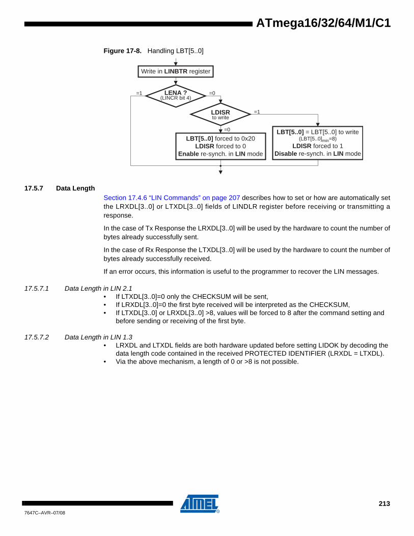
ATmega16/32/64/M1/C1
Figure 17-8. Handling LBT[5..0]
17.5.7 Data LengthSection 17.4.6 “LIN Commands” on page 207 describes how to set or how are automatically setthe LRXDL[3..0] or LTXDL[3..0] fields of LINDLR register before receiving or transmitting aresponse.
In the case of Tx Response the LRXDL[3..0] will be used by the hardware to count the number ofbytes already successfully sent.
In the case of Rx Response the LTXDL[3..0] will be used by the hardware to count the number ofbytes already successfully received.
If an error occurs, this information is useful to the programmer to recover the LIN messages.
17.5.7.1 Data Length in LIN 2.1• If LTXDL[3..0]=0 only the CHECKSUM will be sent,• If LRXDL[3..0]=0 the first byte received will be interpreted as the CHECKSUM,• If LTXDL[3..0] or LRXDL[3..0] >8, values will be forced to 8 after the command setting and
before sending or receiving of the first byte.
17.5.7.2 Data Length in LIN 1.3• LRXDL and LTXDL fields are both hardware updated before setting LIDOK by decoding the
data length code contained in the received PROTECTED IDENTIFIER (LRXDL = LTXDL). • Via the above mechanism, a length of 0 or >8 is not possible.
Write in LINBTR register
LENA ?(LINCR bit 4)
LDISRto write
=0
=0
=1
LBT[5..0] forced to 0x20LDISR forced to 0
Enable re-synch. in LIN mode
LBT[5..0] = LBT[5..0] to write(LBT[5..0]min=8)
LDISR forced to 1Disable re-synch. in LIN mode
=1
2137647C–AVR–07/08

17.5.7.3 Data Length in Rx Response
Figure 17-9. LIN2.1 - Rx Response - No error
• The user initializes LRXDL field before setting the Rx Response command,• After setting the Rx Response command, LTXDL is reset by hardware,• LRXDL field will remain unchanged during Rx (during busy signal),• LTXDL field will count the number of received bytes (during busy signal),• If an error occurs, Rx stops, the corresponding error flag is set and LTXDL will give the num-
ber of received bytes without error,• If no error occurs, LRXOK is set after the reception of the CHECKSUM, LRXDL will be
unchanged (and LTXDL = LRXDL).
17.5.7.4 Data Length in Tx Response
Figure 17-10. LIN1.3 - Tx Response - No error
• The user initializes LTXDL field before setting the Tx Response command,• After setting the Tx Response command, LRXDL is reset by hardware,• LTXDL will remain unchanged during Tx (during busy signal),• LRXDL will count the number of transmitted bytes (during busy signal),• If an error occurs, Tx stops, the corresponding error flag is set and LRXDL will give the num-
ber of transmitted bytes without error,• If no error occurs, LTXOK is set after the transmission of the CHECKSUM, LTXDL will be
unchanged (and LRXDL = LTXDL).
DATA-0 DATA-1 DATA-2 DATA-3 CHECKSUM
LINDLR=0x?4LCMD2..0=000b
LIN bus
LRXDL (*) 4
1? 0
LBUSY
LTXDL (*) 2 3 4
1st Byte 2 nd Byte 3 rd Byte 4 th ByteLIDOK LRXOK
LCMD=Rx Response
(*) : LRXDL & LTXDL updated by user
DATA-0 DATA-1 DATA-2 DATA-3 CHECKSUM
LCMD2..0=000b
LIN bus
LBUSY
1st Byte 2 nd Byte 3 rd Byte 4 th ByteLIDOK LTXOK
14 0LRXDL (*) 2 3 4
LCMD=Tx Response
(*) : LRXDL & LTXDL updated by Rx Response or Tx Response task
LTXDL (*) 4
2147647C–AVR–07/08
ATmega16/32/64/M1/C1

ATmega16/32/64/M1/C1
17.5.7.5 Data Length after Error
Figure 17-11. Tx Response - Error
Note: Information on response (ex: error on byte) is only available at the end of the serialization/de-seri-alization of the byte.
17.5.7.6 Data Length in UART Mode• The UART mode forces LRXDL and LTXDL to 0 and disables the writing in LINDLR register,• Note that after reset, LRXDL and LTXDL are also forced to 0.
17.5.8 xxOK Flags There are three xxOK flags in LINSIR register:
• LIDOK: LIN IDentifier OKIt is set at the end of the header, either by the Tx Header function or by the Rx Header. In LIN 1.3, before generating LIDOK, the controller updates the LRXDL & LTXDL fields in LINDLR register.It is not driven in UART mode.
• LRXOK: LIN RX response completeIt is set at the end of the response by the Rx Response function in LIN mode and once a character is received in UART mode.
• LTXOK: LIN TX response completeIt is set at the end of the response by the Tx Response function in LIN mode and once a character has been sent in UART mode.
These flags can generate interrupts if the corresponding enable interrupt bit is set in the LINE-NIR register (see Section 17.5.13 “Interrupts” on page 217).
17.5.9 xxERR FlagsLERR bit of the LINSIR register is an logical ‘OR’ of all the bits of LINERR register (see Section17.5.13 “Interrupts” on page 217). There are eight flags:
• LBERR = LIN Bit ERRor. A unit that is sending a bit on the bus also monitors the bus. A LIN bit error will be flagged when the bit value that is monitored is different from the bit value that is sent. After detection of a LIN bit error the transmission is aborted.
• LCERR = LIN Checksum ERRor.A LIN checksum error will be flagged if the inverted modulo-256 sum of all received data bytes (and the protected identifier in LIN 2.1) added to the checksum does not result in 0xFF.
• LPERR = LIN Parity ERRor (identifier).A LIN parity error in the IDENTIFIER field will be flagged if the value of the parity bits does not match with the identifier value. (See LP[1:0] bits in Section 17.6.8 “LIN Identifier Register - LINIDR” on page 225). A LIN slave application does not distinguish between corrupted par-ity bits and a corrupted identifier. The hardware does not undertake any correction. How-
DATA-0 DATA-1
LCMD2..0=000b
LIN bus
LBUSY
1st Byte 2 nd Byte 3 rd ByteLERR
14 0LRXDL 2
LCMD=Tx Response
LTXDL 4
DATA-2ERROR
2157647C–AVR–07/08

ever, the LIN slave application has to solve this as:- known identifier (parity bits corrupted),- or corrupted identifier to be ignored,- or new identifier.
• LSERR = LIN Synchronization ERRor.A LIN synchronization error will be flagged if a slave detects the edges of the SYNCH field outside the given tolerance.
• LFERR = LIN Framing ERRor.A framing error will be flagged if dominant STOP bit is sampled.Same function in UART mode.
• LTOERR = LIN Time Out ERRor.A time-out error will be flagged if the MESSAGE frame is not fully completed within the max-imum length T Frame_Maximum by any slave task upon transmission of the SYNCH and IDENTI-FIER fields (see Section 17.5.10 “Frame Time Out” on page 216).
• LOVERR = LIN OVerrun ERRor.Overrun error will be flagged if a new command (other than LIN Abort) is entered while ‘Busy signal’ is present.In UART mode, an overrun error will be flagged if a received byte overwrites the byte stored in the serial input buffer.
• LABORT LIN abort transfer reflects a previous LIN Abort command (LCMD[2..0] = 000) while ‘Busy signal’ is present.
After each LIN error, the LIN controller stops its previous activity and returns to its withdrawalmode (LCMD[2..0] = 000 b) as illustrated in Figure 17-11 on page 215.
Writing 1 in LERR of LINSIR register resets LERR bit and all the bits of the LINERR register.
17.5.10 Frame Time OutAccording to the LIN protocol, a frame time-out error is flagged if: T Frame > T Frame_Maximum. Thisfeature is implemented in the LIN/UART controller.
Figure 17-12. LIN timing and frame time-out
BREAKField
SYNCField
CHECKSUMField
DATA-0FieldField
IDENTIFIERPROTECTED
DATA-nField
T ResponseT Header
T Frame
T Header_Maximum
T Header_Maximum + T Response_Maximum
1.4 x T Header_Nominal
1.4 x T Response_NominalT Response_Maximum
T Frame_Maximum
=
=
=
Maximun before Time-out
T Header_Nominal
T Header_Nominal + T Response_Nominal
34 x T Bit
10 ( Number_of_Data + 1 ) x T BitT Response_Nominal
T Frame_Nominal
=
=
=
Nominal
2167647C–AVR–07/08
ATmega16/32/64/M1/C1

ATmega16/32/64/M1/C1
17.5.11 Break-in-dataAccording to the LIN protocol, the LIN/UART controller can detect the BREAK/SYNC fieldsequence even if the break is partially superimposed with a byte of the response. When aBREAK/SYNC field sequence happens, the transfer in progress is aborted and the processing ofthe new frame starts.
• On slave node(s), an error is generated (i.e. LBERR in case of Tx Response or LFERR in case of Rx Response). Information on data error is also available, refer to the Section 17.5.7.5.
• On master node, the user (code) is responsible for this aborting of frame. To do this, the master task has first to abort the on-going communication (clearing LCMD bits - LIN Abort command) and then to apply the Tx Header command. In this case, the abort error flag - LABORT - is set.
On the slave node, the BREAK detection is processed with the synchronization setting availablewhen the LIN/UART controller processed the (aborted) response. But the re-synchronizationrestarts as usual. Due to a possible difference of timing reference between the BREAK field andthe rest of the frame, the time-out values can be slightly inaccurate.
17.5.12 ChecksumThe last field of a frame is the checksum.
In LIN 2.1, the checksum contains the inverted eight bit sum with carry over all data bytes andthe protected identifier. This calculation is called enhanced checksum.
In LIN 1.3, the checksum contains the inverted eight bit sum with carry over all data bytes. Thiscalculation is called classic checksum.
Frame identifiers 60 (0x3C) to 61 (0x3D) shall always use classic checksum
17.5.13 InterruptsAs shown in Figure 17-13 on page 218, the four communication flags of the LINSIR register arecombined to drive two interrupts. Each of these flags have their respective enable interrupt bit inLINENIR register.
(see Section 17.5.8 “xxOK Flags” on page 215 and Section 17.5.9 “xxERR Flags” on page 215).
CHECKSUM 255 unsigned char DATA n0
n
∑⎝ ⎠⎜ ⎟⎜ ⎟⎛ ⎞
PROTECTED ID.+⎝ ⎠⎜ ⎟⎜ ⎟⎛ ⎞
unsigned char DATA n0
n
∑⎝ ⎠⎜ ⎟⎜ ⎟⎛ ⎞
PROTECTED ID.+⎝ ⎠⎜ ⎟⎜ ⎟⎛ ⎞
8»⎝ ⎠⎜ ⎟⎜ ⎟⎛ ⎞
+⎝ ⎠⎜ ⎟⎜ ⎟⎛ ⎞
–=
CHECKSUM 255 unsigned char DATA n0
n
∑⎝ ⎠⎜ ⎟⎜ ⎟⎛ ⎞
unsigned char DATA n0
n
∑⎝ ⎠⎜ ⎟⎜ ⎟⎛ ⎞
8»⎝ ⎠⎜ ⎟⎜ ⎟⎛ ⎞
+⎝ ⎠⎜ ⎟⎜ ⎟⎛ ⎞
–=
2177647C–AVR–07/08

Figure 17-13. LIN Interrupt Mapping
17.5.14 Message FilteringMessage filtering based upon the whole identifier is not implemented. Only a status for frameheaders having 0x3C, 0x3D, 0x3E and 0x3F as identifier is available in the LINSIR register.
The LIN protocol says that a message with an identifier from 60 (0x3C) up to 63 (0x3F) uses aclassic checksum (sum over the data bytes only). Software will be responsible for switching cor-rectly the LIN13 bit to provide/check this expected checksum (the insertion of the ID field in thecomputation of the CRC is set - or not - just after entering the Rx or Tx Response command).
17.5.15 Data Management
17.5.15.1 LIN FIFO Data BufferTo preserve register allocation, the LIN data buffer is seen as a FIFO (with address pointeraccessible). This FIFO is accessed via the LINDX[2..0] field of LINSEL register through the LIN-DAT register.
LINDX[2..0], the data index, is the address pointer to the required data byte. The data byte canbe read or written. The data index is automatically incremented after each LINDAT access if theLAINC (active low) bit is cleared. A roll-over is implemented, after data index=7 it is dataindex=0. Otherwise, if LAINC bit is set, the data index needs to be written (updated) before eachLINDAT access.
The first byte of a LIN frame is stored at the data index=0, the second one at the data index=1,and so on. Nevertheless, LINSEL must be initialized by the user before use.
LIDOKLINSIR.2
LTXOKLINSIR.1
LRXOKLINSIR.0
LABORTLINERR.7
LTOERRLINERR.6
LOVERRLINERR.5
LERRLINSIR.3
LIN IT
LENERR
LFERRLINERR.4
LSERRLINERR.3
LPERRLINERR.2
LCERRLINERR.1
LBERRLINERR.0
LIN ERR
LENIDOK
LINENIR.2
LENTXOK
LINENIR.1
LENRXOK
LINENIR.0LINENIR.3
Table 17-4. Frame Status
LIDST[2..0] Frame Status0xx b No specific identifier
100 b 60 (0x3C) identifier
101 b 61 (0x3D) identifier
110 b 62 (0x3E) identifier
111 b 63 (0x3F) identifier
2187647C–AVR–07/08
ATmega16/32/64/M1/C1

ATmega16/32/64/M1/C1
17.5.15.2 UART Data RegisterThe LINDAT register is the data register (no buffering - no FIFO). In write access, LINDAT will befor data out and in read access, LINDAT will be for data in.
In UART mode the LINSEL register is unused.
17.5.16 OCD SupportThis chapter describes the behavior of the LIN/UART controller stopped by the OCD (i.e. I/Oview behavior in AVR Studio)
1. LINCR:- LINCR[6..0] are R/W accessible,- LSWRES always is a self-reset bit (needs 1 micro-controller cycle to execute)
2. LINSIR:- LIDST[2..0] and LBUSY are always Read accessible,- LERR & LxxOK bit are directly accessible (unlike in execution, set or cleared directly by writing 1 or 0).- Note that clearing LERR resets all LINERR bits and setting LERR sets all LINERR bits.
3. LINENR:- All bits are R/W accessible.
4. LINERR:- All bits are R/W accessible,- Note that LINERR bits are ORed to provide the LERR interrupt flag of LINSIR.
5. LINBTR:- LBT[5..0] are R/W access only if LDISR is set,- If LDISR is reset, LBT[5..0] are unchangeable.
6. LINBRRH & LINBRRL:- All bits are R/W accessible.
7. LINDLR:- All bits are R/W accessible.
8. LINIDR:- LID[5..0] are R/W accessible,- LP[1..0] are Read accessible and are always updated on the fly.
9. LINSEL:- All bits are R/W accessible.
10. LINDAT:- All bits are in R/W accessible,- Note that LAINC has no more effect on the auto-incrementation and the access to the full FIFO is done setting LINDX[2..0] of LINSEL.
Note: When a debugger break occurs, the state machine of the LIN/UART controller is stopped (included frame time-out) and further communication may be corrupted.
2197647C–AVR–07/08

17.6 LIN / UART Register Description
17.6.1 LIN Control Register - LINCR
• Bit 7 - LSWRES: Software Reset– 0 = No action,– 1 = Software reset (this bit is self-reset at the end of the reset procedure).
• Bit 6 - LIN13: LIN 1.3 mode– 0 = LIN 2.1 (default),– 1 = LIN 1.3.
• Bit 5:4 - LCONF[1:0]: Configurationa. LIN mode (default = 00):
–00 = LIN Standard configuration (listen mode “off”, CRC “on” & Frame_Time_Out “on”,– 01 = No CRC, no Time out (listen mode “off”),
Table 17-5. LIN/UART Register Bits Summary
Name Bit 7 Bit 6 Bit 5 Bit 4 Bit 3 Bit 2 Bit 1 Bit 0
LINCRLSWRES LIN13 LCONF1 LCONF0 LENA LCMD2 LCMD1 LCMD0
0 R/W 0 R/W 0 R/W 0 R/W 0 R/W 0 R/W 0 R/W 0 R/W
LINSIRLIDST2 LIDST1 LIDST0 LBUSY LERR LIDOK LTXOK LRXOK
0 R 0 R 0 R 0 R 0 R/Wone 0 R/Wone 0 R/Wone 0 R/Wone
LINENIR— — — — LENERR LENIDOK LENTXOK LENRXOK
0 R 0 R 0 R 0 R 0 R/W 0 R/W 0 R/W 0 R/W
LINERRLABORT LTOERR LOVERR LFERR LSERR LPERR LCERR LBERR
0 R 0 R 0 R 0 R 0 R 0 R 0 R 0 R
LINBTRLDISR LBT5 LBT4 LBT3 LBT2 LBT1 LBT0
0 R/W 0 R 1 R/(W) 0 R/(W) 0 R/(W) 0 R/(W) 0 R/(W) 0 R/(W)
LINBRRLLDIV7 LDIV6 LDIV5 LDIV4 LDIV3 LDIV2 LDIV1 LDIV0
0 R/W 0 R/W 0 R/W 0 R/W 0 R/W 0 R/W 0 R/W 0 R/W
LINBRRH— — — — LDIV11 LDIV10 LDIV9 LDIV8
0 R 0 R 0 R 0 R 0 R/W 0 R/W 0 R/W 0 R/W
LINDLRLTXDL3 LTXDL2 LTXDL1 LTXDL0 LRXDL3 LRXDL2 LRXDL1 LRXDL0
0 R/W 0 R/W 0 R/W 0 R/W 0 R/W 0 R/W 0 R/W 0 R/W
LINIDRLP1 LP0 LID5/LDL1 LID4/LDL0 LID3 LID2 LID1 LID0
1 R 0 R 0 R/W 0 R/W 0 R/W 0 R/W 0 R/W 0 R/W
LINSEL— — — — LAINC LINDX2 LINDX1 LINDX0
0 R 0 R 0 R 0 R 0 R/W 0 R/W 0 R/W 0 R/W
LINDATLDATA7 LDATA6 LDATA5 LDATA4 LDATA3 LDATA2 LDATA1 LDATA0
0 R/W 0 R/W 0 R/W 0 R/W 0 R/W 0 R/W 0 R/W 0 R/W
Bit 7 6 5 4 3 2 1 0
LSWRES LIN13 LCONF1 LCONF0 LENA LCMD2 LCMD1 LCMD0 LINCRRead/Write R/W R/W R/W R/W R/W R/W R/W R/W
Initial Value 0 0 0 0 0 0 0 0
2207647C–AVR–07/08
ATmega16/32/64/M1/C1

ATmega16/32/64/M1/C1
– 10 = No Frame_Time_Out (listen mode “off” & CRC “on”),– 11 = Listening mode (CRC “on” & Frame_Time_Out “on”).
b. UART mode (default = 00):– 00 = 8-bit, no parity (listen mode “off”),– 01 = 8-bit, even parity (listen mode “off”),– 10 = 8-bit, odd parity (listen mode “off”),– 11 = Listening mode, 8-bit, no parity.
• Bit 3 - LENA: Enable– 0 = Disable (both LIN and UART modes),– 1 = Enable (both LIN and UART modes).
• Bit 2:0 - LCMD[2..0]: Command and modeThe command is only available if LENA is set.
–000 = LIN Rx Header - LIN abort,– 001 = LIN Tx Header,– 010 = LIN Rx Response,– 011 = LIN Tx Response,– 100 = UART Rx & Tx Byte disable,– 11x = UART Rx Byte enable,– 1x1 = UART Tx Byte enable.
17.6.2 LIN Status and Interrupt Register - LINSIR
• Bits 7:5 - LIDST[2:0]: Identifier Status– 0xx = no specific identifier,– 100 = Identifier 60 (0x3C),– 101 = Identifier 61 (0x3D),– 110 = Identifier 62 (0x3E),– 111 = Identifier 63 (0x3F).
• Bit 4 - LBUSY: Busy Signal– 0 = Not busy,– 1 = Busy (receiving or transmitting).
• Bit 3 - LERR: Error InterruptIt is a logical OR of LINERR register bits. This bit generates an interrupt if its respective
enable bit - LENERR - is set in LINENIR.
– 0 = No error,
Bit 7 6 5 4 3 2 1 0
LIDST2 LIDST1 LIDST0 LBUSY LERR LIDOK LTXOK LRXOK LINSIRRead/Write R R R R R/Wone R/Wone R/Wone R/Wone
Initial Value 0 0 0 0 0 0 0 0
2217647C–AVR–07/08

– 1 = An error has occurred.The user clears this bit by writing 1 in order to reset this interrupt. Resetting LERR also
resets all LINERR bits.
In UART mode, this bit is also cleared by reading LINDAT.
• Bit 2 - LIDOK: Identifier InterruptThis bit generates an interrupt if its respective enable bit - LENIDOK - is set in LINENIR.
– 0 = No identifier,– 1 = Slave task: Identifier present, master task: Tx Header complete.The user clears this bit by writing 1, in order to reset this interrupt.
• Bit 1 - LTXOK: Transmit Performed InterruptThis bit generates an interrupt if its respective enable bit - LENTXOK - is set in LINENIR.
– 0 = No Tx,– 1 = Tx Response complete.The user clears this bit by writing 1, in order to reset this interrupt.
In UART mode, this bit is also cleared by writing LINDAT.
• Bit 0 - LRXOK: Receive Performed InterruptThis bit generates an interrupt if its respective enable bit - LENRXOK - is set in LINENIR.
– 0 = No Rx – 1 = Rx Response complete.The user clears this bit by writing 1, in order to reset this interrupt.
In UART mode, this bit is also cleared by reading LINDAT.
17.6.3 LIN Enable Interrupt Register - LINENIR
• Bits 7:4 - Reserved BitsThese bits are reserved for future use. For compatibility with future devices, they must be
written to zero when LINENIR is written.
• Bit 3 - LENERR: Enable Error Interrupt– 0 = Error interrupt masked,– 1 = Error interrupt enabled.
• Bit 2 - LENIDOK: Enable Identifier Interrupt– 0 = Identifier interrupt masked,– 1 = Identifier interrupt enabled.
• Bit 1 - LENTXOK: Enable Transmit Performed Interrupt
Bit 7 6 5 4 3 2 1 0
- - - - LENERR LENIDOK LENTXOK LENRXOK LINENIRRead/Write R R R R R/W R/W R/W R/W
Initial Value 0 0 0 0 0 0 0 0
2227647C–AVR–07/08
ATmega16/32/64/M1/C1

ATmega16/32/64/M1/C1
– 0 = Transmit performed interrupt masked,– 1 = Transmit performed interrupt enabled.
• Bit 0 - LENRXOK: Enable Receive Performed Interrupt– 0 = Receive performed interrupt masked,– 1 = Receive performed interrupt enabled.
17.6.4 LIN Error Register - LINERR
• Bit 7 - LABORT: Abort Flag– 0 = No warning,– 1 = LIN abort command occurred.This bit is cleared when LERR bit in LINSIR is cleared.
• Bit 6 - LTOERR: Frame_Time_Out Error Flag– 0 = No error,– 1 = Frame_Time_Out error.This bit is cleared when LERR bit in LINSIR is cleared.
• Bit 5 - LOVERR: Overrun Error Flag– 0 = No error,– 1 = Overrun error.This bit is cleared when LERR bit in LINSIR is cleared.
• Bit 4 - LFERR: Framing Error Flag– 0 = No error,– 1 = Framing error.This bit is cleared when LERR bit in LINSIR is cleared.
• Bit 3 - LSERR: Synchronization Error Flag– 0 = No error,– 1 = Synchronization error.This bit is cleared when LERR bit in LINSIR is cleared.
• Bit 2 - LPERR: Parity Error Flag– 0 = No error,– 1 = Parity error.This bit is cleared when LERR bit in LINSIR is cleared.
• Bit 1 - LCERR: Checksum Error Flag– 0 = No error,
Bit 7 6 5 4 3 2 1 0
LABORT LTOERR LOVERR LFERR LSERR LPERR LCERR LBERR LINERRRead/Write R R R R R R R R
Initial Value 0 0 0 0 0 0 0 0
2237647C–AVR–07/08

– 1 = Checksum error.This bit is cleared when LERR bit in LINSIR is cleared.
• Bit 0 - LBERR: Bit Error Flag– 0 = no error,– 1 = Bit error.This bit is cleared when LERR bit in LINSIR is cleared.
17.6.5 LIN Bit Timing Register - LINBTR
• Bit 7 - LDISR: Disable Bit Timing Re synchronization– 0 = Bit timing re-synchronization enabled (default),– 1 = Bit timing re-synchronization disabled.
• Bits 5:0 - LBT[5:0]: LIN Bit TimingGives the number of samples of a bit.
sample-time = (1 / fclki/o ) x (LDIV[11..0] + 1)
Default value: LBT[6:0]=32 — Min. value: LBT[6:0]=8 — Max. value: LBT[6:0]=63
17.6.6 LIN Baud Rate Register - LINBRR
• Bits 15:12 - Reserved BitsThese bits are reserved for future use. For compatibility with future devices, they must be
written to zero when LINBRR is written.
• Bits 11:0 - LDIV[11:0]: Scaling of clki/o FrequencyThe LDIV value is used to scale the entering clki/o frequency to achieve appropriate LIN or
UART baud rate.
17.6.7 LIN Data Length Register - LINDLR
• Bits 7:4 - LTXDL[3:0]: LIN Transmit Data Length
Bit 7 6 5 4 3 2 1 0
LDISR - LBT5 LBT4 LBT3 LBT2 LBT1 LBT0 LINBTRRead/Write R/W R R/(W) R/(W) R/(W) R/(W) R/(W) R/(W)
Initial Value 0 0 1 0 0 0 0 0
Bit 7 6 5 4 3 2 1 0
LDIV7 LDIV6 LDIV5 LDIV4 LDIV3 LDIV2 LDIV1 LDIV0 LINBRRL- - - - LDIV11 LDIV10 LDIV9 LDIV8 LINBRRH
Bit 15 14 13 12 11 10 9 8
Read/Write R/W R/W R/W R/W R/W R/W R/W R/W
Initial Value 0 0 0 0 0 0 0 0
Bit 7 6 5 4 3 2 1 0
LTXDL3 LTXDL2 LTXDL1 LTXDL0 LRXDL3 LRXDL2 LRXDL1 LRXDL0 LINDLRRead/Write R/W R/W R/W R/W R/W R/W R/W R/W
Initial Value 0 0 0 0 0 0 0 0
2247647C–AVR–07/08
ATmega16/32/64/M1/C1
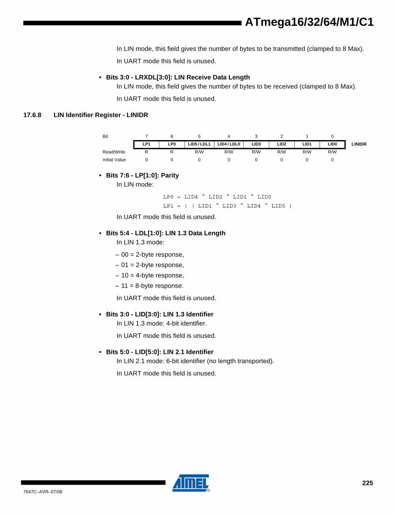
ATmega16/32/64/M1/C1
In LIN mode, this field gives the number of bytes to be transmitted (clamped to 8 Max).
In UART mode this field is unused.
• Bits 3:0 - LRXDL[3:0]: LIN Receive Data LengthIn LIN mode, this field gives the number of bytes to be received (clamped to 8 Max).
In UART mode this field is unused.
17.6.8 LIN Identifier Register - LINIDR
• Bits 7:6 - LP[1:0]: ParityIn LIN mode:
LP0 = LID4 ^ LID2 ^ LID1 ^ LID0
LP1 = ! ( LID1 ^ LID3 ^ LID4 ^ LID5 )
In UART mode this field is unused.
• Bits 5:4 - LDL[1:0]: LIN 1.3 Data LengthIn LIN 1.3 mode:
– 00 = 2-byte response,– 01 = 2-byte response,– 10 = 4-byte response,– 11 = 8-byte response.
In UART mode this field is unused.
• Bits 3:0 - LID[3:0]: LIN 1.3 IdentifierIn LIN 1.3 mode: 4-bit identifier.
In UART mode this field is unused.
• Bits 5:0 - LID[5:0]: LIN 2.1 IdentifierIn LIN 2.1 mode: 6-bit identifier (no length transported).
In UART mode this field is unused.
Bit 7 6 5 4 3 2 1 0
LP1 LP0 LID5 / LDL1 LID4 / LDL0 LID3 LID2 LID1 LID0 LINIDRRead/Write R R R/W R/W R/W R/W R/W R/W
Initial Value 0 0 0 0 0 0 0 0
2257647C–AVR–07/08

17.6.9 LIN Data Buffer Selection Register - LINSEL
• Bits 7:4 - Reserved BitsThese bits are reserved for future use. For compatibility with future devices, they must be
written to zero when LINSEL is written.
• Bit 3 - LAINC: Auto Increment of Data Buffer IndexIn LIN mode:
– 0 = Auto incrementation of FIFO data buffer index (default),– 1 = No auto incrementation.
In UART mode this field is unused.
• Bits 2:0 - LINDX 2:0: FIFO LIN Data Buffer IndexIn LIN mode: location (index) of the LIN response data byte into the FIFO data buffer. The
FIFO data buffer is accessed through LINDAT.
In UART mode this field is unused.
17.6.10 LIN Data Register - LINDAT
• Bits 7:0 - LDATA[7:0]: LIN Data In / Data outIn LIN mode: FIFO data buffer port.
In UART mode: data register (no data buffer - no FIFO).
– In Write access, data out.– In Read access, data in.
Bit 7 6 5 4 3 2 1 0
- - - - LAINC LINDX2 LINDX1 LINDX0 LINSELRead/Write - - - - R/W R/W R/W R/W
Initial Value - - - - 0 0 0 0
Bit 7 6 5 4 3 2 1 0
LDATA7 LDATA6 LDATA5 LDATA4 LDATA3 LDATA2 LDATA1 LDATA0 LINDATRead/Write R/W R/W R/W R/W R/W R/W R/W R/W
Initial Value 0 0 0 0 0 0 0 0
2267647C–AVR–07/08
ATmega16/32/64/M1/C1

ATmega16/32/64/M1/C1
18. Analog to Digital Converter - ADC
18.1 Features• 10-bit Resolution• 0.5 LSB Integral Non-linearity• ± 2 LSB Absolute Accuracy• 8- 250 µs Conversion Time• Up to 125 kSPS at Maximum Resolution• 11 Multiplexed Single Ended Input Channels• 3 Differential input channels with accurate (5%) programmable gain 5, 10, 20 and 40• Optional Left Adjustment for ADC Result Readout• 0 - VCC ADC Input Voltage Range• Selectable 2.56 V ADC Reference Voltage• Free Running or Single Conversion Mode• ADC Start Conversion by Auto Triggering on Interrupt Sources• Interrupt on ADC Conversion Complete• Sleep Mode Noise Canceler• Temperature Sensor• LiN Address Sense (ISRC Voltage Measurement)• Vcc Voltage Measurement
The ATmega16/32/64/M1/C1 features a 10-bit successive approximation ADC. The ADC is con-nected to an 15-channel Analog Multiplexer which allows eleven single-ended input. The single-ended voltage inputs refer to 0V (GND).
The device also supports 3 differential voltage input amplifiers which are equipped with a pro-grammable gain stage, providing amplification steps of 14dB (5x), 20 dB (10x), 26 dB (20x), or32dB (40x) on the differential input voltage before the A/D conversion. On the amplified chan-nels, 8-bit resolution can be expected.
The ADC contains a Sample and Hold circuit which ensures that the input voltage to the ADC isheld at a constant level during conversion. A block diagram of the ADC is shown in Figure 18-1.
The ADC has a separate analog supply voltage pin, AVCC. AVCC must not differ more than ±0.3V from VCC. See the paragraph “ADC Noise Canceler” on page 234 on how to connect thispin.
Internal reference voltages of nominally 2.56V or AVCC are provided On-chip. The voltage refer-ence may be externally decoupled at the AREF pin by a capacitor for better noise performance.
2277647C–AVR–07/08

Figure 18-1. Analog to Digital Converter Block Schematic
MUX2 MUX1 MUX0MUX3REFS1 REFS0 ADLAR MUX4 ADPS2 ADPS1 ADPS0ADIEADEN ADSC ADATE ADIF
ADMUX ADCSRA
ADTS2 ADTS1 ADTS0ADASCR- - -
ADCSRB
Edge Detector
Sou
rces
ADC0ADC1ADC2ADC3ADC4ADC5
AMP2-/ADC6ADC7
AMP1-/ADC8AMP1+/ADC9
ADC10AMP0-AMP0+
-+
AMP0CSR
-+
AMP1CSR
+
-SAR
10
10
ADCH
ADCL
Coarse/Fine DAC10
Internal 2.56VReference
REFS0 REFS1
AREF / ISRC
AVCC
PRESCALERCK
CKADC
CONTROL
CKADC
ADC CONVERSIONCOMPLETE IRQ
GNDBandgap
ADATE
ADTS3
Temp SensorVCC/4
ISRC
AMP2+-+
AMP2CSR
AREFEN
ISRCEN
CurrentSource
ISRC
2287647C–AVR–07/08
ATmega16/32/64/M1/C1

ATmega16/32/64/M1/C1
18.2 OperationThe ADC converts an analog input voltage to a 10-bit digital value through successive approxi-mation. The minimum value represents GND and the maximum value represents the voltage onthe AREF pin minus 1 LSB. Optionally, AVCC or an internal 2.56V reference voltage may be con-nected to the AREF pin by writing to the REFSn bits in the ADMUX Register. The internalvoltage reference may thus be decoupled by an external capacitor at the AREF pin to improvenoise immunity.
The analog input channel are selected by writing to the MUX bits in ADMUX. Any of the ADCinput pins, as well as GND and a fixed bandgap voltage reference, can be selected as singleended inputs to the ADC.
The ADC is enabled by setting the ADC Enable bit, ADEN in ADCSRA. Voltage reference is setby the REFS1 and REFS0 bits in ADMUX register, whatever the ADC is enabled or not. TheADC does not consume power when ADEN is cleared, so it is recommended to switch off theADC before entering power saving sleep modes.
The ADC generates a 10-bit result which is presented in the ADC Data Registers, ADCH andADCL. By default, the result is presented right adjusted, but can optionally be presented leftadjusted by setting the ADLAR bit in ADMUX.
If the result is left adjusted and no more than 8-bit precision is required, it is sufficient to readADCH. Otherwise, ADCL must be read first, then ADCH, to ensure that the content of the DataRegisters belongs to the same conversion. Once ADCL is read, ADC access to Data Registersis blocked. This means that if ADCL has been read, and a conversion completed before ADCHis read, neither register is updated and the result from the conversion is lost. When ADCH isread, ADC access to the ADCH and ADCL Registers is re-enabled.
The ADC has its own interrupt which can be triggered when a conversion completes. The ADCaccess to the Data Registers is prohibited between reading of ADCH and ADCL, the interruptwill trigger even if the result is lost.
18.3 Starting a ConversionA single conversion is started by writing a logical one to the ADC Start Conversion bit, ADSC.This bit stays high as long as the conversion is in progress and will be cleared by hardwarewhen the conversion is completed. If a different data channel is selected while a conversion is inprogress, the ADC will finish the current conversion before performing the channel change.
Alternatively, a conversion can be triggered automatically by various sources. Auto Triggering isenabled by setting the ADC Auto Trigger Enable bit, ADATE in ADCSRA. The trigger source isselected by setting the ADC Trigger Select bits, ADTS in ADCSRB (See description of the ADTSbits for a list of the trigger sources). When a positive edge occurs on the selected trigger signal,the ADC prescaler is reset and a conversion is started. This provides a method of starting con-versions at fixed intervals. If the trigger signal is still set when the conversion completes, a newconversion will not be started. If another positive edge occurs on the trigger signal during con-version, the edge will be ignored. Note that an interrupt flag will be set even if the specificinterrupt is disabled or the Global Interrupt Enable bit in SREG is cleared. A conversion can thusbe triggered without causing an interrupt. However, the interrupt flag must be cleared in order totrigger a new conversion at the next interrupt event.
2297647C–AVR–07/08

Figure 18-2. ADC Auto Trigger Logic
Using the ADC Interrupt Flag as a trigger source makes the ADC start a new conversion as soonas the ongoing conversion has finished. The ADC then operates in Free Running mode, con-stantly sampling and updating the ADC Data Register. The first conversion must be started bywriting a logical one to the ADSC bit in ADCSRA. In this mode the ADC will perform successiveconversions independently of whether the ADC Interrupt Flag, ADIF is cleared or not. The freerunning mode is not allowed on the amplified channels.
If Auto Triggering is enabled, single conversions can be started by writing ADSC in ADCSRA toone. ADSC can also be used to determine if a conversion is in progress. The ADSC bit will beread as one during a conversion, independently of how the conversion was started.
18.4 Prescaling and Conversion Timing
Figure 18-3. ADC Prescaler
By default, the successive approximation circuitry requires an input clock frequency between 50kHz and 2 MHz to get maximum resolution. If a lower resolution than 10 bits is needed, the inputclock frequency to the ADC can be higher than 2 MHz to get a higher sample rate.
The ADC module contains a prescaler, which generates an acceptable ADC clock frequencyfrom any CPU frequency above 100 kHz. The prescaling is set by the ADPS bits in ADCSRA.The prescaler starts counting from the moment the ADC is switched on by setting the ADEN bitin ADCSRA. The prescaler keeps running for as long as the ADEN bit is set, and is continuouslyreset when ADEN is low.
ADSC
ADIF
SOURCE 1
SOURCE n
ADTS[2:0]
CONVERSIONLOGIC
PRESCALER
START CLKADC
.
.
.
. EDGEDETECTOR
ADATE
7-BIT ADC PRESCALER
ADC CLOCK SOURCE
CK
ADPS0ADPS1ADPS2
CK
/128
CK
/2
CK
/4
CK
/8
CK
/16
CK
/32
CK
/64
ResetADENSTART
2307647C–AVR–07/08
ATmega16/32/64/M1/C1
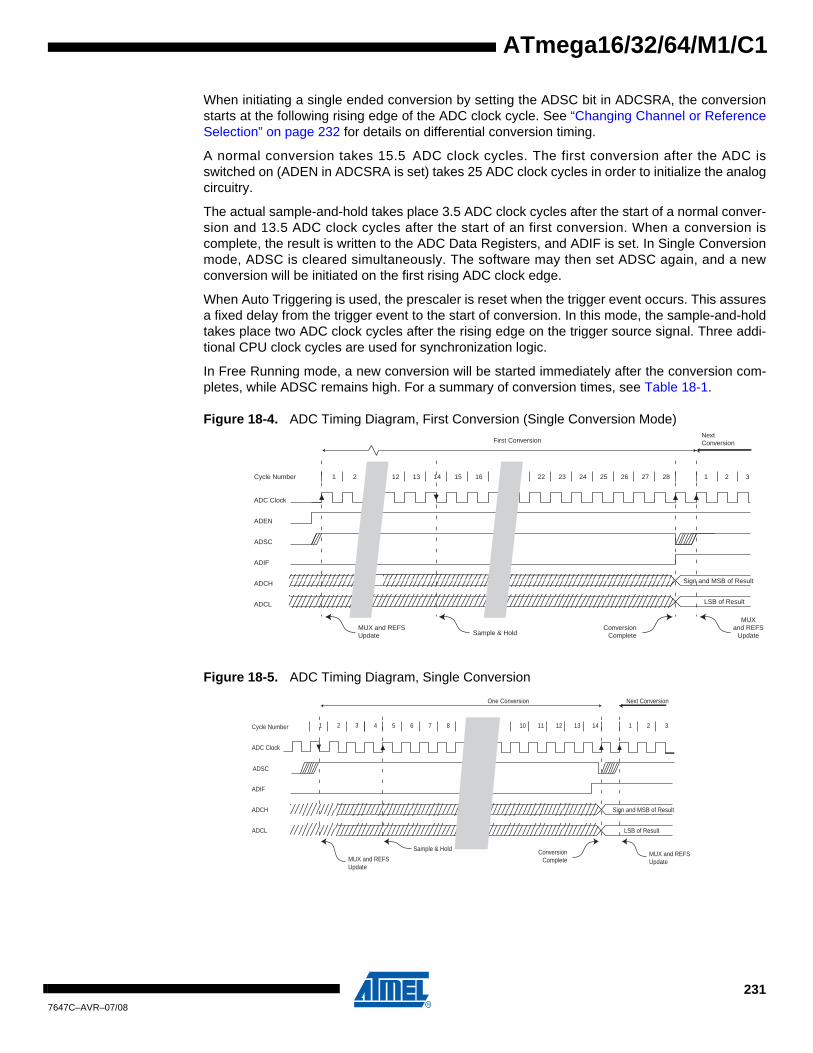
ATmega16/32/64/M1/C1
When initiating a single ended conversion by setting the ADSC bit in ADCSRA, the conversionstarts at the following rising edge of the ADC clock cycle. See “Changing Channel or ReferenceSelection” on page 232 for details on differential conversion timing.
A normal conversion takes 15.5 ADC clock cycles. The first conversion after the ADC isswitched on (ADEN in ADCSRA is set) takes 25 ADC clock cycles in order to initialize the analogcircuitry.
The actual sample-and-hold takes place 3.5 ADC clock cycles after the start of a normal conver-sion and 13.5 ADC clock cycles after the start of an first conversion. When a conversion iscomplete, the result is written to the ADC Data Registers, and ADIF is set. In Single Conversionmode, ADSC is cleared simultaneously. The software may then set ADSC again, and a newconversion will be initiated on the first rising ADC clock edge.
When Auto Triggering is used, the prescaler is reset when the trigger event occurs. This assuresa fixed delay from the trigger event to the start of conversion. In this mode, the sample-and-holdtakes place two ADC clock cycles after the rising edge on the trigger source signal. Three addi-tional CPU clock cycles are used for synchronization logic.
In Free Running mode, a new conversion will be started immediately after the conversion com-pletes, while ADSC remains high. For a summary of conversion times, see Table 18-1.
Figure 18-4. ADC Timing Diagram, First Conversion (Single Conversion Mode)
Figure 18-5. ADC Timing Diagram, Single Conversion
Sign and MSB of Result
LSB of Result
ADC Clock
ADSC
Sample & Hold
ADIF
ADCH
ADCL
Cycle Number
ADEN
1 2 12 13 14 15 16 22 23 24 25 26 27 28 1 2
First ConversionNextConversion
3
MUX and REFSUpdate
MUXand REFS
UpdateConversion
Complete
4 5 6 7 8 10 11 12 13 14
Sign and MSB of Result
LSB of Result
ADC Clock
ADSC
ADIF
ADCH
ADCL
Cycle Number 1 2
One Conversion Next Conversion
3
Sample & Hold
MUX and REFSUpdate
ConversionComplete
MUX and REFSUpdate
1 2 3
2317647C–AVR–07/08

Figure 18-6. ADC Timing Diagram, Auto Triggered Conversion
Figure 18-7. ADC Timing Diagram, Free Running Conversion
18.5 Changing Channel or Reference SelectionThe MUXn and REFS1:0 bits in the ADMUX Register are single buffered through a temporaryregister to which the CPU has random access. This ensures that the channels and referenceselection only takes place at a safe point during the conversion. The channel and referenceselection is continuously updated until a conversion is started. Once the conversion starts, thechannel and reference selection is locked to ensure a sufficient sampling time for the ADC. Con-tinuous updating resumes in the last eight ADC clock cycle before the conversion completes(ADIF in ADCSRA is set). Note that the conversion starts on the second following rising CPUclock edge after ADSC is written. The user is thus advised not to write new channel or referenceselection values to ADMUX until two ADC clock cycle after ADSC is written.
Table 18-1. ADC Conversion Time
Condition First Conversion
Normal Conversion,
Single EndedAuto Triggered
Conversion
Sample & Hold(Cycles from Start of Conversion) 13.5 3.5 2
Conversion Time(Cycles) 25 15.5 16
1 2 3 4 5 6 7 8 11 12 13 14
Sign and MSB of Result
LSB of Result
ADC Clock
TriggerSource
ADIF
ADCH
ADCL
Cycle Number 1 2
One Conversion Next Conversion
ConversionCompletePrescaler
Reset
ADATE
PrescalerReset
Sample &Hold
MUX and REFS Update
12 13 14
Sign and MSB of Result
LSB of Result
ADC Clock
ADSC
ADIF
ADCH
ADCL
Cycle Number1 2
One Conversion Next Conversion
3 4
ConversionComplete
Sample & Hold
MUX and REFSUpdate
5
2327647C–AVR–07/08
ATmega16/32/64/M1/C1

ATmega16/32/64/M1/C1
If Auto Triggering is used, the exact time of the triggering event can be indeterministic. Specialcare must be taken when updating the ADMUX Register, in order to control which conversionwill be affected by the new settings.
If both ADATE and ADEN is written to one, an interrupt event can occur at any time. If theADMUX Register is changed in this period, the user cannot tell if the next conversion is basedon the old or the new settings. ADMUX can be safely updated in the following ways:
1. When ADATE or ADEN is cleared.2. During conversion, with taking care of the trigger source event, when it is possible.3. After a conversion, before the interrupt flag used as trigger source is cleared.
When updating ADMUX in one of these conditions, the new settings will affect the next ADCconversion.
18.5.1 ADC Input Channels
When changing channel selections, the user should observe the following guidelines to ensurethat the correct channel is selected:• In Single Conversion mode, always select the channel before starting the conversion. The
channel selection may be changed one ADC clock cycle after writing one to ADSC. However, the simplest method is to wait for the conversion to complete before changing the channel selection.
• In Free Running mode, always select the channel before starting the first conversion. The channel selection may be changed one ADC clock cycle after writing one to ADSC. However, the simplest method is to wait for the first conversion to complete, and then change the channel selection. Since the next conversion has already started automatically, the next result will reflect the previous channel selection. Subsequent conversions will reflect the new channel selection.
• In Free Running mode, because the amplifier clear the ADSC bit at the end of an amplified conversion, it is not possible to use the free running mode, unless ADSC bit is set again by soft at the end of each conversion.
18.5.2 ADC Voltage Reference
The reference voltage for the ADC (VREF) indicates the conversion range for the ADC. Singleended channels that exceed VREF will result in codes close to 0x3FF. VREF can be selected aseither AVCC, internal 2.56V reference, or external AREF pin.
AVCC is connected to the ADC through a passive switch. The internal 2.56V reference is gener-ated from the internal bandgap reference (VBG) through an internal amplifier. In either case, theexternal AREF pin is directly connected to the ADC, and the reference voltage can be mademore immune to noise by connecting a capacitor between the AREF pin and ground. VREF canalso be measured at the AREF pin with a high impedant voltmeter. Note that VREF is a highimpedant source, and only a capacitive load should be connected in a system.
If the user has a fixed voltage source connected to the AREF pin, the user may not use the otherreference voltage options in the application, as they will be shorted to the external voltage. If noexternal voltage is applied to the AREF pin, the user may switch between AVCC and 2.56V asreference selection. The first ADC conversion result after switching reference voltage sourcemay be inaccurate, and the user is advised to discard this result.
AREF pin is alternate function with ISRC Current Source output. When current source isselected, the AREF pin is not connected to the internal reference voltage network. See AREFENand ISRCEN bits in Section “ADC Control and Status Register B– ADCSRB”, page 244.
2337647C–AVR–07/08

If differential channels are used, the selected reference should not be closer to AVCC than indi-cated in Table 25-3 on page 308.
18.6 ADC Noise CancelerThe ADC features a noise canceler that enables conversion during sleep mode to reduce noiseinduced from the CPU core and other I/O peripherals. The noise canceler can be used with ADCNoise Reduction and Idle mode. To make use of this feature, the following procedure should beused:
a. Make sure the ADATE bit is reset.b. Make sure that the ADC is enabled and is not busy converting. Single Conversion
mode must be selected and the ADC conversion complete interrupt must be enabled.
c. Enter ADC Noise Reduction mode (or Idle mode). The ADC will start a conversion once the CPU has been halted.
d. If no other interrupts occur before the ADC conversion completes, the ADC inter-rupt will wake up the CPU and execute the ADC Conversion Complete interrupt routine. If another interrupt wakes up the CPU before the ADC conversion is com-plete, that interrupt will be executed, and an ADC Conversion Complete interrupt request will be generated when the ADC conversion completes. The CPU will remain in active mode until a new sleep command is executed.
Note that the ADC will not be automatically turned off when entering other sleep modes than Idlemode and ADC Noise Reduction mode. The user is advised to write zero to ADEN before enter-ing such sleep modes to avoid excessive power consumption.
If the ADC is enabled in such sleep modes and the user wants to perform differential conver-sions, the user is advised to switch the ADC off and on after waking up from sleep to prompt anextended conversion to get a valid result.
18.6.1 Analog Input Circuitry
The analog input circuitry for single ended channels is illustrated in Figure 18-8. An analogsource applied to ADCn is subjected to the pin capacitance and input leakage of that pin, regard-less of whether that channel is selected as input for the ADC. When the channel is selected, thesource must drive the S/H capacitor through the series resistance (combined resistance in theinput path).
The ADC is optimized for analog signals with an output impedance of approximately 10 kΩ orless. If such a source is used, the sampling time will be negligible. If a source with higher imped-ance is used, the sampling time will depend on how long time the source needs to charge theS/H capacitor, with can vary widely. The user is recommended to only use low impedant sourceswith slowly varying signals, since this minimizes the required charge transfer to the S/Hcapacitor.
If differential gain channels are used, the input circuitry looks somewhat different, althoughsource impedances of a few hundred kΩ or less is recommended.
Signal components higher than the Nyquist frequency (fADC/2) should not be present for eitherkind of channels, to avoid distortion from unpredictable signal convolution. The user is advisedto remove high frequency components with a low-pass filter before applying the signals asinputs to the ADC.
2347647C–AVR–07/08
ATmega16/32/64/M1/C1

ATmega16/32/64/M1/C1
Figure 18-8. Analog Input Circuitry
18.6.2 Analog Noise Canceling Techniques
Digital circuitry inside and outside the device generates EMI which might affect the accuracy ofanalog measurements. If conversion accuracy is critical, the noise level can be reduced byapplying the following techniques:
1. Keep analog signal paths as short as possible. Make sure analog tracks run over theanalog ground plane, and keep them well away from high-speed switching digitaltracks.
2. The AVCC pin on the device should be connected to the digital VCC supply voltagevia an RC network.
3. Use the ADC noise canceler function to reduce induced noise from the CPU.4. If any ADC port pins are used as digital outputs, it is essential that these do not
switch while a conversion is in progress.
18.6.3 Offset Compensation Schemes
The gain stage has a built-in offset cancellation circuitry that nulls the offset of differential mea-surements as much as possible. The remaining offset in the analog path can be measureddirectly by shortening both differential inputs using the AMPxIS bit with both inputs unconnected.(See “Amplifier 0 Control and Status register – AMP0CSR” on page 251., See “Amplifier 1 Con-trol and Status register – AMP1CSR” on page 252.and See “Amplifier 1 Control and Statusregister – AMP1CSR” on page 252.). This offset residue can be then subtracted in software fromthe measurement results. Using this kind of software based offset correction, offset on any chan-nel can be reduced below one LSB.
18.6.4 ADC Accuracy Definitions
An n-bit single-ended ADC converts a voltage linearly between GND and VREF in 2n steps(LSBs). The lowest code is read as 0, and the highest code is read as 2n-1.
Several parameters describe the deviation from the ideal behavior:• Offset: The deviation of the first transition (0x000 to 0x001) compared to the ideal transition
(at 0.5 LSB). Ideal value: 0 LSB.
ADCn
IIH
1..100 kΩCS/H= 14 pF
VCC/2
IIL
2357647C–AVR–07/08

Figure 18-9. Offset Error
• Gain Error: After adjusting for offset, the Gain Error is found as the deviation of the last transition (0x3FE to 0x3FF) compared to the ideal transition (at 1.5 LSB below maximum). Ideal value: 0 LSB
Figure 18-10. Gain Error
• Integral Non-linearity (INL): After adjusting for offset and gain error, the INL is the maximum deviation of an actual transition compared to an ideal transition for any code. Ideal value: 0 LSB.
Output Code
VREF Input Voltage
Ideal ADC
Actual ADC
OffsetError
Output Code
VREF Input Voltage
Ideal ADC
Actual ADC
GainError
2367647C–AVR–07/08
ATmega16/32/64/M1/C1

ATmega16/32/64/M1/C1
Figure 18-11. Integral Non-linearity (INL)
• Differential Non-linearity (DNL): The maximum deviation of the actual code width (the interval between two adjacent transitions) from the ideal code width (1 LSB). Ideal value: 0 LSB.
Figure 18-12. Differential Non-linearity (DNL)
• Quantization Error: Due to the quantization of the input voltage into a finite number of codes, a range of input voltages (1 LSB wide) will code to the same value. Always ± 0.5 LSB.
• Absolute Accuracy: The maximum deviation of an actual (unadjusted) transition compared to an ideal transition for any code. This is the compound effect of offset, gain error, differential error, non-linearity, and quantization error. Ideal value: ± 0.5 LSB.
18.7 ADC Conversion ResultAfter the conversion is complete (ADIF is high), the conversion result can be found in the ADCResult Registers (ADCL, ADCH).
For single ended conversion, the result is:
Output Code
VREF Input Voltage
Ideal ADC
Actual ADC
INL
Output Code
0x3FF
0x000
0 VREF Input Voltage
DNL
1 LSB
2377647C–AVR–07/08

where VIN is the voltage on the selected input pin and VREF the selected voltage reference (seeTable 18-4 on page 242 and Table 18-5 on page 243). 0x000 represents analog ground, and0x3FF represents the selected reference voltage.
If differential channels are used, the result is:
where VPOS is the voltage on the positive input pin, VNEG the voltage on the negative input pin,GAIN the selected gain factor and VREF the selected voltage reference. The result is presentedin two’s complement form, from 0x200 (-512d) through 0x1FF (+511d). Note that if the userwants to perform a quick polarity check of the result, it is sufficient to read the MSB of the result(ADC9 in ADCH). If the bit is one, the result is negative, and if this bit is zero, the result is posi-tive. Figure 18-13 shows the decoding of the differential input range.
Table 82 shows the resulting output codes if the differential input channel pair (ADCn - ADCm) isselected with a reference voltage of VREF.
Figure 18-13. Differential Measurement Range
ADCVIN 1023⋅
VREF--------------------------=
ADCVPOS VNEG–( ) GAIN 512⋅ ⋅
VREF------------------------------------------------------------------------=
0
Output Code
0x1FF
0x000
VREFDifferential InputVoltage (Volts)
0x3FF
0x200
- VREF /Gain/Gain
2387647C–AVR–07/08
ATmega16/32/64/M1/C1
ATmega16/32/64/M1/C1
Example 1:– ADMUX = 0xED (ADC3 - ADC2, 10x gain, 2.56V reference, left adjusted result) – Voltage on ADC3 is 300 mV, voltage on ADC2 is 500 mV. – ADCR = 512 * 10 * (300 - 500) / 2560 = -400 = 0x270 – ADCL will thus read 0x00, and ADCH will read 0x9C.
Writing zero to ADLAR right adjusts the result: ADCL = 0x70, ADCH = 0x02.
Example 2:– ADMUX = 0xFB (ADC3 - ADC2, 1x gain, 2.56V reference, left adjusted result) – Voltage on ADC3 is 300 mV, voltage on ADC2 is 500 mV. – ADCR = 512 * 1 * (300 - 500) / 2560 = -41 = 0x029.– ADCL will thus read 0x40, and ADCH will read 0x0A.
Writing zero to ADLAR right adjusts the result: ADCL = 0x00, ADCH = 0x29.
18.8 Temperature MeasurementThe temperature measurement is based on an on-chip temperature sensor that is coupled to asingle ended ADC input. MUX[4..0] bits in ADMUX register enables the temperature sensor. Theinternal 2.56V voltage reference must also be selected for the ADC voltage reference source inthe temperature sensor measurement. When the temperature sensor is enabled, the ADC con-verter can be used in single conversion mode to measure the voltage over the temperaturesensor.
As shown Figure 18-14, the temperature sensor is followed by a driver. This driver is enabledwhen ADMUX value selects the temperature sensor as ADC input See “ADC Input ChannelSelection” on page 243. The propagation delay of this driver is approximatively 2µS. Thereforetwo successive conversions are required. The correct temperature measurement will be the sec-ond one.
One can also reduce this timing to one conversion by setting the ADMUX during the previousconversion. Indeed the ADMUX can be programmed to select the temperature sensor just afterthe beginning of the previous conversion start event and then the driver will be enabled 2 µSbefore sampling and hold phase of temperature sensor measurement. See “Changing Channelor Reference Selection” on page 232.
Table 18-2. Correlation Between Input Voltage and Output Codes
VADCn Read code Corresponding decimal value
VADCm + VREF /GAIN 0x1FF 511
VADCm + 0.999 VREF /GAIN 0x1FF 511
VADCm + 0.998 VREF /GAIN 0x1FE 510
... ... ...
VADCm + 0.001 VREF /GAIN 0x001 1
VADCm 0x000 0
VADCm - 0.001 VREF /GAIN 0x3FF -1
... ... ...
VADCm - 0.999 VREF /GAIN 0x201 -511
VADCm - VREF /GAIN 0x200 -512
2397647C–AVR–07/08

Figure 18-14. Temperature Sensor Block Diagram
The measured voltage has a linear relationship to the temperature as described in Table 18-3 onpage 240. The voltage sensitivity is approximately 1 mV/°C and the accuracy of the temperaturemeasurement is +/- 10°C after bandgap calibration.
The values described in Table 18-3 on page 240 are typical values. However, due to the processvariation the temperature sensor output voltage varies from one chip to another. To be capableof achieving more accurate results, the temperature measurement can be calibrated in the appli-cation software.
18.8.1 User CalibrationThe software calibration requires that a calibration value is measured and stored in a register orEEPROM for each chip. The software calibration can be done utilizing the formula:
T = { [ (ADCH << 8) | ADCL ] - TOS } / k
where ADCH & ADCL are the ADC data registers, k is a fixed coefficient and TOS is the temper-ature sensor offset value determined and stored into EEPROM.
18.8.2 Manufacturing CalibrationOne can also use the calibration values available in the signature row See “Reading the Signa-ture Row from Software” on page 286.
The calibration values are determined from values measured during test at room temperaturewhich is approximatively +25°C and during test at hot temperature which is approximatively+125°C. Calibration measures are done at Vcc = 3V and with ADC in internal Vref (2.56V) mode.
The temperature in Celsius degrees can be calculated utilizing the formula:
T = { [ (ADCH << 8) | ADCL ] -273 } *TSGAIN + TSOFFSET
Where:
Table 18-3. Temperature vs. Sensor Output Voltage (Typical Case)
Temperature / °C -40 °C +25 °C +125 °C
Voltage / mV 600 mV 762 mv 1012 mV
TemperatureSensor
ADCInputMultiplexer
ADMUX
to samplingand hold
G=1
Enable whenADMUX = Temp. Sensor input
2407647C–AVR–07/08
ATmega16/32/64/M1/C1

ATmega16/32/64/M1/C1
a. ADCH & ADCL are the ADC data registers,b. TSGAIN is the temperature sensor gain (constant 1, or unsigned fixed point num-
ber, 0x80 = decimal 1.0)c. TSOFFSET is the temperature sensor offset correction term (2. complement
signed byte)
18.9 ADC Register DescriptionThe ADC of the ATmega16/32/64/M1/C1 is controlled through 3 different registers. The ADC-SRA and The ADCSRB registers which are the ADC Control and Status registers, and theADMUX which allows to select the Vref source and the channel to be converted.
The conversion result is stored on ADCH and ADCL register which contain respectively the mostsignificant bits and the less significant bits.
2417647C–AVR–07/08

18.9.1 ADC Multiplexer Register – ADMUX
• Bit 7, 6 – REFS1, 0: ADC Vref Selection Bits
These 2 bits determine the voltage reference for the ADC.The different setting are shown in Table 18-4.
If bits REFS1 and REFS0 are changed during a conversion, the change will not take effect untilthis conversion is complete (it means while the ADIF bit in ADCSRA register is set). In case the internal Vref is selected, it is turned ON as soon as an analog feature needed it isset.• Bit 5 – ADLAR: ADC Left Adjust Result
Set this bit to left adjust the ADC result.Clear it to right adjust the ADC result.The ADLAR bit affects the configuration of the ADC result data registers. Changing this bitaffects the ADC data registers immediately regardless of any on going conversion. For a com-plete description of this bit, see Section “ADC Result Data Registers – ADCH and ADCL”,page 245.
Bit 7 6 5 4 3 2 1 0
REFS1 REFS0 ADLAR MUX4 MUX3 MUX2 MUX1 MUX0 ADMUX
Read/Write R/W R/W R/W - R/W R/W R/W R/W
Initial Value 0 0 0 0 0 0 0 0
Table 18-4. ADC Voltage Reference Selection
AREFEN ISRCEN REFS1 REFS0 Description
1 0 0 0 External Vref on AREF pin, Internal Vref is switched off
1 0 0 1 AVcc with external capacitor connected on the AREF pin
0 0 0 1 AVcc (no external capacitor connected on the AREF pin)
1 0 1 0 Reserved
1 0 1 1 Internal 2.56V Reference voltage with external capacitor connected on the AREF pin
0 x 1 1 Internal 2.56V Reference voltage
2427647C–AVR–07/08
ATmega16/32/64/M1/C1

ATmega16/32/64/M1/C1
• Bit 4, 2, 1, 0 – MUX4, MUX3, MUX2, MUX1, MUX0: ADC Channel Selection Bits
These 4 bits determine which analog inputs are connected to the ADC input. The different set-ting are shown in Table 18-5.
If these bits are changed during a conversion, the change will not take effect until this conversionis complete (it means while the ADIF bit in ADCSRA register is set).
18.9.2 ADC Control and Status Register A – ADCSRA
• Bit 7 – ADEN: ADC Enable Bit
Set this bit to enable the ADC.Clear this bit to disable the ADC.Clearing this bit while a conversion is running will take effect at the end of the conversion.
Table 18-5. ADC Input Channel Selection
MUX4 MUX3 MUX2 MUX1 MUX0 Description
0 0 0 0 0 ADC0
0 0 0 0 1 ADC1
0 0 0 1 0 ADC2
0 0 0 1 1 ADC3
0 0 1 0 0 ADC4
0 0 1 0 1 ADC5
0 0 1 1 0 ADC6
0 0 1 1 1 ADC7
0 1 0 0 0 ADC8
0 1 0 0 1 ADC9
0 1 0 1 0 ADC10
0 1 0 1 1 Temp Sensor
0 1 1 0 0 VCC/4
0 1 1 0 1 ISRC
0 1 1 1 0 AMP0
0 1 1 1 1 AMP1 (- is ADC8, + is ADC9)
1 0 0 0 0 AMP2 (- is ADC6)
1 0 0 0 1 Bandgap
1 0 0 1 0 GND
1 0 0 1 1 Reserved
1 0 1 x x Reserved
1 1 x x x Reserved
Bit 7 6 5 4 3 2 1 0
ADEN ADSC ADATE ADIF ADIE ADPS2 ADPS1 ADPS0 ADCSRA
Read/Write R/W R/W R/W R R/W R/W R/W R/W
Initial Value 0 0 0 0 0 0 0 0
2437647C–AVR–07/08

• Bit 6– ADSC: ADC Start Conversion Bit
Set this bit to start a conversion in single conversion mode or to start the first conversion in freerunning mode.Cleared by hardware when the conversion is complete. Writing this bit to zero has no effect.The first conversion performs the initialization of the ADC.• Bit 5 – ADATE: ADC Auto trigger Enable Bit
Set this bit to enable the auto triggering mode of the ADC.Clear it to return in single conversion mode.In auto trigger mode the trigger source is selected by the ADTS bits in the ADCSRB register.See Table 18-7 on page 245.• Bit 4– ADIF: ADC Interrupt Flag
Set by hardware as soon as a conversion is complete and the Data register are updated with theconversion result.Cleared by hardware when executing the corresponding interrupt handling vector.Alternatively, ADIF can be cleared by writing it to logical one.• Bit 3– ADIE: ADC Interrupt Enable Bit
Set this bit to activate the ADC end of conversion interrupt.Clear it to disable the ADC end of conversion interrupt.• Bit 2, 1, 0– ADPS2, ADPS1, ADPS0: ADC Prescaler Selection Bits
These 3 bits determine the division factor between the system clock frequency and input clock ofthe ADC.The different setting are shown in Table 18-6.
18.9.3 ADC Control and Status Register B– ADCSRB
• Bit 7 – ADHSM: ADC High Speed Mode
Writing this bit to one enables the ADC High Speed mode. Set this bit if you wish to convert withan ADC clock frequency higher than 200KHz.
Clear this bit to reduce the power consumption of the ADC when the ADC clock frequency islower than 200KHz.
Table 18-6. ADC Prescaler Selection
ADPS2 ADPS1 ADPS0 Division Factor
0 0 0 2
0 0 1 2
0 1 0 4
0 1 1 8
1 0 0 16
1 0 1 32
1 1 0 64
1 1 1 128
Bit 7 6 5 4 3 2 1 0
ADHSM ISRCEN AREFEN - ADTS3 ADTS2 ADTS1 ADTS0 ADCSRB
Read/Write R/W R/W R/W R R/W R/W R/W R/W
Initial Value 0 0 0 0 0 0 0 0
2447647C–AVR–07/08
ATmega16/32/64/M1/C1

ATmega16/32/64/M1/C1
• Bit 6 – ISRCEN: Current Source Enable
Set this bit to source a 100µA current to the AREF pin.Clear this bit to use AREF pin as Analog Reference pin.• Bit 5 – AREFEN: Analog Reference pin Enable
Set this bit to connect the internal AREF circuit to the AREF pin.Clear this bit to disconnect the internal AREF circuit from the AREF pin.• Bit 4 – Res: Reserved Bit
This bit is unused bit in the ATmega16/32/64/M1/C1, and will always read as zero.• Bit 3, 2, 1, 0– ADTS3:ADTS0: ADC Auto Trigger Source Selection Bits
These bits are only necessary in case the ADC works in auto trigger mode. It means if ADATEbit in ADCSRA register is set.
In accordance with the Table 18-7, these 3 bits select the interrupt event which will generate thetrigger of the start of conversion. The start of conversion will be generated by the rising edge ofthe selected interrupt flag whether the interrupt is enabled or not. In case of trig on PSCnASYevent, there is no flag. So in this case a conversion will start each time the trig event appearsand the previous conversion is completed..
18.9.4 ADC Result Data Registers – ADCH and ADCL
When an ADC conversion is complete, the conversion results are stored in these two result dataregisters.
When the ADCL register is read, the two ADC result data registers can’t be updated until theADCH register has also been read.Consequently, in 10-bit configuration, the ADCL register must be read first before the ADCH.
Table 18-7. ADC Auto Trigger Source Selection
ADTS3 ADTS2 ADTS1 ADTS0 Description
0 0 0 0 Free Running Mode
0 0 0 1 External Interrupt Request 0
0 0 1 0 Timer/Counter0 Compare Match
0 0 1 1 Timer/Counter0 Overflow
0 1 0 0 Timer/Counter1 Compare Match B
0 1 0 1 Timer/Counter1 Overflow
0 1 1 0 Timer/Counter1 Capture Event
0 1 1 1 PSC Module 0 Synchronization Signal
1 0 0 0 PSC Module 1 Synchronization Signal
1 0 0 1 PSC Module 2 Synchronization Signal
1 0 1 0 Analog comparator 0
1 0 1 1 Analog comparator 1
1 1 0 0 Analog comparator 2
1 1 0 1 Analog comparator 3
1 1 1 0 Reserved
1 1 1 1 Reserved
2457647C–AVR–07/08

Nevertheless, to work easily with only 8-bit precision, there is the possibility to left adjust theresult thanks to the ADLAR bit in the ADCSRA register. Like this, it is sufficient to only readADCH to have the conversion result.
18.9.4.1 ADLAR = 0
18.9.4.2 ADLAR = 1
18.9.5 Digital Input Disable Register 0 – DIDR0
• Bit 7:0 – ADC7D..ADC0D, ACMPN0D, ACMPN1D, ACMPN2D, ACMPN3D, ACMP2D, AMP2ND:ADC7:0, ACMPN0, ACMPN1, ACMPN2, ACMPN3, ACMP2, AMP2N Digital Input Disable
When this bit is written logic one, the digital input buffer on the corresponding ADC pin is dis-abled. The corresponding PIN Register bit will always read as zero when this bit is set. When ananalog signal is applied to the ADC7..0 pin and the digital input from this pin is not needed, thisbit should be written logic one to reduce power consumption in the digital input buffer.
18.9.6 Digital Input Disable Register 1– DIDR1
• Bit 6:0 – ADC10D..8D, ACMP0D, ACMP1D, ACMP3D, AMP0PD, AMP0ND, AMP1PD, AMP1ND, AMP2PD:ADC10..8, ACMP0, ACMP1, ACMP3, AMP0P, AMP0N, AMP1P, AMP1N, AMP2P Digital Input Disable
When this bit is written logic one, the digital input buffer on the corresponding ADC pin is dis-abled. The corresponding PIN Register bit will always read as zero when this bit is set. When an
Bit 7 6 5 4 3 2 1 0
- - - - - - ADC9 ADC8 ADCHADC7 ADC6 ADC5 ADC4 ADC3 ADC2 ADC1 ADC0 ADCL
Read/Write R R R R R R R R
R R R R R R R R
Initial Value 0 0 0 0 0 0 0 0
0 0 0 0 0 0 0 0
Bit 7 6 5 4 3 2 1 0
ADC9 ADC8 ADC7 ADC6 ADC5 ADC4 ADC3 ADC2 ADCHADC1 ADC0 - - - - - - ADCL
Read/Write R R R R R R R R
R R R R R R R R
Initial Value 0 0 0 0 0 0 0 0
0 0 0 0 0 0 0 0
Bit 7 6 5 4 3 2 1 0
ADC7D ADC6DACMPN1DAMP2ND
ADC5DACMPN0D
ADC4D ADC3DACMPN2D
ADC2DACMP2D
ADC1D ADC0DACMPN3D
DIDR0
Read/Write R/W R/W R/W R/W R/W R/W R/W R/W
Initial Value 0 0 0 0 0 0 0 0
Bit 7 6 5 4 3 2 1 0
- AMP2PD ACMP0D AMP0PD AMP0ND ADC10DACMP1D
ADC9DAMP1PDACMP3D
ADC8DAMP1ND
DIDR1
Read/Write - - R/W R/W R/W R/W R/W R/W
Initial Value 0 0 0 0 0 0 0 0
2467647C–AVR–07/08
ATmega16/32/64/M1/C1

ATmega16/32/64/M1/C1
analog signal is applied to an analog pin and the digital input from this pin is not needed, this bitshould be written logic one to reduce power consumption in the digital input buffer.
18.10 AmplifierThe ATmega16/32/64/M1/C1 features three differential amplified channels with programmable5, 10, 20, and 40 gain stage.
Because the amplifiers are switching capacitor amplifiers, they need to be clocked by a synchro-nization signal called in this document the amplifier synchronization clock. To ensure anaccurate result, the amplifier input needs to have a quite stable input value during at least 4Amplifier synchronization clock periods. The amplifiers can run with a clock frequency of up to250 kHz (typical value).
To ensure an accurate result, the amplifier input needs to have a quite stable input value at thesampling point during at least 4 amplifier synchronization clock periods.
Amplified conversions can be synchronized to PSC events (See “Synchronization SourceDescription in One Ramp Mode” on page 151 and “Synchronization Source Description in Cen-tered Mode” on page 151) or to the internal clock CKADC equal to eighth the ADC clockfrequency. In case the synchronization is done the ADC clock divided by 8, this synchronizationis done automatically by the ADC interface in such a way that the sample-and-hold occurs at aspecific phase of CKADC2. A conversion initiated by the user (i.e., all single conversions, and thefirst free running conversion) when CKADC2 is low will take the same amount of time as a singleended conversion (13 ADC clock cycles from the next prescaled clock cycle). A conversion initi-ated by the user when CKADC2 is high will take 14 ADC clock cycles due to the synchronizationmechanism.
The normal way to use the amplifier is to select a synchronization clock via the AMPxTS1:0 bitsin the AMPxCSR register. Then the amplifier can be switched on, and the amplification is doneon each synchronization event.
In order to start an amplified Analog to Digital Conversion on the amplified channel, the ADMUXmust be configured as specified on Table 18-5 on page 243.
The ADC starting requirement is done by setting the ADSC bit of the ADCSRA Register.
Until the conversion is not achieved, it is not possible to start a conversion on another channel.
In order to have a better understanding of the functioning of the amplifier synchronization, twotiming diagram examples are shown Figure 18-15 and Figure 18-16.
As soon as a conversion is requested thanks to the ADSC bit, the Analog to Digital Conversionis started. In case the amplifier output is modified during the sample phase of the ADC, the on-going conversion is aborted and restarted as soon as the output of the amplifier is stable. Thisensure a fast response time. The only precaution to take is to be sure that the trig signal (PSC)frequency is lower than ADCclk/4.
2477647C–AVR–07/08

Figure 18-15. Amplifier synchronization timing diagramWith change on analog input signal
Valid sample
Delta V4th stable sample
Signal to bemeasured
AMPLI_clk(Sync Clock)
CK ADC
PSCn_ASYPSCBlock
ADSC
ADCActivity
ADC
ADCSampling
ADCConv
ADCSampling
ADCConv
ADC ResultReady
ADC ResultReady
2487647C–AVR–07/08
ATmega16/32/64/M1/C1

ATmega16/32/64/M1/C1
Figure 18-16. Amplifier synchronization timing diagramADSC is set when the amplifier output is changing due to the amplifier clock switch
In order to have a better understanding of the functioning of the amplifier synchronization, a tim-ing diagram example is shown Figure 18-15.
It is also possible to auto trigger conversion on the amplified channel. In this case, the conver-sion is started at the next amplifier clock event following the last auto trigger event selectedthanks to the ADTS bits in the ADCSRB register. In auto trigger conversion, the free runningmode is not possible unless the ADSC bit in ADCSRA is set by soft after each conversion.
The block diagram of the two amplifiers is shown on Figure 18-17.
Valid sample
Signal to bemeasured
AMPLI_clk(Sync Clock)
CK ADC
PSCn_ASYPSCBlock
ADSC
ADCActivity
ADC
ADCSampling
ADCConv
ADCSampling
ADCConv
ADCSamplingAborted
ADC ResultReady
ADC ResultReady
2497647C–AVR–07/08

Figure 18-17. Amplifiers block diagram
AMP0TS1 AMP0TS0AMP0EN AMP0IS AMP0G1 AMP0G0
AMP0CSR
+
-SA
MP
LIN
GAMP0+
AMP0-
Toward ADC MUX(AMP0)
Amplifier 0Clock
011001
00
AMPCMP0 AMP0TS2
AMP1TS1 AMP1TS0AMP1EN AMP1IS AMP1G1 AMP1G0
AMP1CSR
+
-SA
MP
LIN
GAMP1+
AMP1-
Toward ADC MU(AMP1)
Amplifier 1Clock
011001
00
AMPCMP1 AMP1TS2
AMP2TS1 AMP2TS0AMP2EN AMP2IS AMP2G1 AMP2G0
AMP2CSR
+
-SA
MP
LIN
GAMP2+
AMP2-
Toward ADC MU(AMP2)
Amplifier 2Clock
ADCK/8
PSS0PSS1PSS2
AMPCMP2 AMP2TS2
Timer 0 Compare MatchTimer 0 OverflowTimer 1 Compare MatchTimer 1 Overflow
ADCK/8
PSS0PSS1PSS2
Timer 0 Compare MatchTimer 0 OverflowTimer 1 Compare MatchTimer 1 Overflow
ADCK/8
PSS0PSS1PSS2
Timer 0 Compare MatchTimer 0 OverflowTimer 1 Compare MatchTimer 1 Overflow
2507647C–AVR–07/08
ATmega16/32/64/M1/C1

ATmega16/32/64/M1/C1
18.11 Amplifier Control RegistersThe configuration of the amplifiers are controlled via two dedicated registers AMP0CSR andAMP1CSR. Then the start of conversion is done via the ADC control and status registers.
The conversion result is stored on ADCH and ADCL register which contain respectively the mostsignificant bits and the less significant bits.
18.11.1 Amplifier 0 Control and Status register – AMP0CSR
• Bit 7 – AMP0EN: Amplifier 0 Enable Bit
Set this bit to enable the Amplifier 0.Clear this bit to disable the Amplifier 0.Clearing this bit while a conversion is running will take effect at the end of the conversion.
Warning: Always clear AMP0TS0:1 when clearing AMP0EN.• Bit 6 – AMP0IS: Amplifier 0 Input Shunt
Set this bit to short-circuit the Amplifier 0 input.Clear this bit to normally use the Amplifier 0.• Bit 5, 4 – AMP0G1, 0: Amplifier 0 Gain Selection Bits
These 2 bits determine the gain of the amplifier 0.The different setting are shown in Table 18-8.
To ensure an accurate result, after the gain value has been changed, the amplifier input needsto have a quite stable input value during at least 4 Amplifier synchronization clock periods.• Bit 3 – AMPCMP0: Amplifier 0 - Comparator 0 connection
Set this bit to connect the amplifier 0 to the comparator 0 positive input. In this configuration thecomparator clock is twice the amplifier clock.Clear this bit to normally use the Amplifier 0.
• Bit 2:0 – AMP0TS2,AMP0TS1,AMP0TS0: Amplifier 0 Clock Source Selection Bits
Bit 7 6 5 4 3 2 1 0
AMP0EN AMP0IS AMP0G1 AMP0G0 AMPCMP0 AMP0TS2 AMP0TS1 AMP0TS0 AMP0CSR
Read/Write R/W R/W R/W R/W R/W R/W R/W R/W
Initial Value 0 0 0 0 0 0 0 0
Table 18-8. Amplifier 0 Gain Selection
AMP0G1 AMP0G0 Description
0 0 Gain 5
0 1 Gain 10
1 0 Gain 20
1 1 Gain 40
2517647C–AVR–07/08

In accordance with the Table 18-9, these 3 bits select the event which will generate the clock forthe amplifier 0. This clock source is necessary to start the conversion on the amplified channel.
18.11.2 Amplifier 1 Control and Status register – AMP1CSR
• Bit 7 – AMP1EN: Amplifier 1 Enable Bit
Set this bit to enable the Amplifier 1.Clear this bit to disable the Amplifier 1.Clearing this bit while a conversion is running will take effect at the end of the conversion.
Warning: Always clear AMP1TS0:1 when clearing AMP1EN.• Bit 6 – AMP1IS: Amplifier 1 Input Shunt
Set this bit to short-circuit the Amplifier 1 input.Clear this bit to normally use the Amplifier 1.• Bit 5, 4 – AMP1G1, 0: Amplifier 1 Gain Selection Bits
These 2 bits determine the gain of the amplifier 1.The different setting are shown in Table 18-10.
To ensure an accurate result, after the gain value has been changed, the amplifier input needsto have a quite stable input value during at least 4 Amplifier synchronization clock periods.• Bit 3 – AMPCMP1: Amplifier 1 - Comparator 1 connection
Table 18-9. AMP0 Clock Source Selection
AMP0TS2 AMP0TS1 AMP0TS0 Clock Source
0 0 0 ADC Clock/8
0 0 1 Timer/Counter0 Compare Match
0 1 0 Timer/Counter0 Overflow
0 1 1 Timer/Counter1 Compare Match B
1 0 0 Timer/Counter1 Overflow
1 0 1 PSC Module 0 Synchronization Signal (PSS0)
1 1 0 PSC Module 1 Synchronization Signal (PSS1)
1 1 1 PSC Module 2 Synchronization Signal (PSS2)
Bit 7 6 5 4 3 2 1 0
AMP1EN AMP1IS AMP1G1 AMP1G0 AMPCMP1 AMP1TS2 AMP1TS1 AMP1TS0 AMP1CSR
Read/Write R/W R/W R/W R/W R/W R/W R/W R/W
Initial Value 0 0 0 0 0 0 0 0
Table 18-10. Amplifier 1 Gain Selection
AMP1G1 AMP1G0 Description
0 0 Gain 5
0 1 Gain 10
1 0 Gain 20
1 1 Gain 40
2527647C–AVR–07/08
ATmega16/32/64/M1/C1

ATmega16/32/64/M1/C1
Set this bit to connect the amplifier 1 to the comparator 1 positive input. In this configuration thecomparator clock is twice amplifier clock.Clear this bit to normally use the Amplifier 1.• Bit 2:0 – AMP1TS2,AMP1TS1, AMP1TS0: Amplifier 1 Clock Source Selection Bits
In accordance with the Table 18-11, these 3 bits select the event which will generate the clockfor the amplifier 1. This clock source is necessary to start the conversion on the amplifiedchannel.
18.11.3 Amplifier 2 Control and Status register – AMP2CSR
• Bit 7 – AMP2EN: Amplifier 2 Enable Bit
Set this bit to enable the Amplifier 2.Clear this bit to disable the Amplifier 2.Clearing this bit while a conversion is running will take effect at the end of the conversion.
Warning: Always clear AMP2TS0:1 when clearing AMP2EN.• Bit 6 – AMP2IS: Amplifier 2 Input Shunt
Set this bit to short-circuit the Amplifier 2 input.Clear this bit to normally use the Amplifier 2.• Bit 5, 4 – AMP2G1, 0: Amplifier 2 Gain Selection Bits
These 2 bits determine the gain of the amplifier 2.The different setting are shown in Table 18-12.
Table 18-11. AMP1 Clock Source Selection
AMP1TS2 AMP1TS1 AMP1TS0 Clock Source
0 0 0 ADC Clock/8
0 0 1 Timer/Counter0 Compare Match
0 1 0 Timer/Counter0 Overflow
0 1 1 Timer/Counter1 Compare Match B
1 0 0 Timer/Counter1 Overflow
1 0 1 PSC Module 0 Synchronization Signal (PSS0)
1 1 0 PSC Module 1 Synchronization Signal (PSS1)
1 1 1 PSC Module 2 Synchronization Signal (PSS2)
Bit 7 6 5 4 3 2 1 0
AMP2EN AMP2IS AMP2G1 AMP2G0 AMPCMP2 AMP2TS2 AMP2TS1 AMP2TS0 AMP2CSR
Read/Write R/W R/W R/W R/W R/W R/W R/W R/W
Initial Value 0 0 0 0 0 0 0 0
Table 18-12. Amplifier 2 Gain Selection
AMP2G1 AMP2G0 Description
0 0 Gain 5
0 1 Gain 10
1 0 Gain 20
1 1 Gain 40
2537647C–AVR–07/08

To ensure an accurate result, after the gain value has been changed, the amplifier input needsto have a quite stable input value during at least 4 Amplifier synchronization clock periods.• Bit 3 – AMPCMP2: Amplifier 2 - Comparator 2 connection
Set this bit to connect the amplifier 2 to the comparator 2 positive input. In this configuration thecomparator clock is twice the amplifier clock.Clear this bit to normally use the Amplifier 2.• Bit 2:0 – AMP2TS2,AMP2TS1, AMP2TS0: Amplifier 2 Clock Source Selection Bits
In accordance with the Table 18-13, these 3 bits select the event which will generate the clockfor the amplifier 1. This clock source is necessary to start the conversion on the amplifiedchannel.
Table 18-13. AMP1 Clock Source Selection
AMP2TS2 AMP2TS1 AMP2TS0 Clock Source
0 0 0 ADC Clock/8
0 0 1 Timer/Counter0 Compare Match
0 1 0 Timer/Counter0 Overflow
0 1 1 Timer/Counter1 Compare Match B
1 0 0 Timer/Counter1 Overflow
1 0 1 PSC Module 0 Synchronization Signal (PSS0)
1 1 0 PSC Module 1 Synchronization Signal (PSS1)
1 1 1 PSC Module 2 Synchronization Signal (PSS2)
2547647C–AVR–07/08
ATmega16/32/64/M1/C1

ATmega16/32/64/M1/C1
19. ISRC - Current Source
19.1 Features• 100µA Constant current source• ± 3% Absolute Accuracy
The ATmega16/32/64/M1/C1 features a 100µA ±3% Current Source. After RESET or up onrequest, the current is flowing through an external resistor. The voltage can be measured on thededicated pin shared with the ADC. Using a resistor in serie with a ≤0.5% tolerance is recom-mended. To protect the device against big values, the ADC must be configured with AVcc asinternal reference to perform the first measurement. Afterwards, another internal reference canbe chosen according to the previous measured value to refine the result.
When ISRCEN bit is set, the ISRC pin sources 100µA. Otherwise this pin keeps its initialfunction.
Figure 19-1. Current Source Block Diagram
19.2 Typical applications
19.2.1 LIN Current SourceDuring the configuration of a LIN node in a cluster, it may be necessary to attribute dynamicallyan unique physical address to every cluster node. The way to do it is not described in the LINprotocol.
The Current Source offers an excellent solution to associate a physical address to the applica-tion supported by the LIN node. A full dynamic node configuration can be used to set-up the LINnodes in a cluster.
AVCC
AREF Internal Circuit
ExternalResistor
ISRCEN AREF / ISRC
100 uA
AREFEN
ADC Input
2557647C–AVR–07/08

ATmega16/32/64/M1/C1 proposes to have an external resistor used in conjunction with the Cur-rent Source. The device measures the voltage to the boundaries of the resistance via the Analogto Digital converter. The resulting voltage defines the physical address that the communicationhandler will use when the node will participate in LIN communication.
In automotive applications, distributed voltages are very disturbed. The internal Current Sourcesolution of ATmega16/32/64/M1/C1 immunizes the address detection against any kind of volt-age variations.
Table 19-1. Example of Resistor Values(±5%) for a 8-address System (AVcc = 5V(1))
Physical Address
Resistor ValueRload (Ohm)
Typical Measured Voltage (V)
Minimum Reading with
a 2.56V ref
Typical Reading with
a 2.56V ref
Maximum Reading with
a 2.56V ref
0 1 000 0.1 40
1 2 200 0.22 88
2 3 300 0.33 132
3 4 700 0.47 188
4 6 800 0.68 272
5 10 000 1 400
6 15 000 1.5 600
7 22 000 2.2 880
2567647C–AVR–07/08
ATmega16/32/64/M1/C1

ATmega16/32/64/M1/C1
Note: 1. 5V range: Max Rload 30KΩ3V range: Max Rload 15KΩ
19.2.2 Current Source for Low Cost TraducerAn external transducer based on variable resistor can be connected to the Current Source. Thisca be for instance:
• A thermistor, or temperature-sensitive resistor, used as a temperature sensor• A CdS photoconductive cell, or luminosity-sensitivity resistor, used as a luminosity sensor.
Using the Current Source with this type of transducer eliminates the need for additional partsotherwise required in resistor network or Wheatstone bridge.
19.2.3 Voltage Reference for External DevicesAn external resistor used in conjunction with the Current Source can be used as voltage refer-ence for external devices. Using a resistor in serie with a lower tolerance than the CurrentSource accuracy (≤2%) is recommended. Table 19-2 gives an example of voltage referencesusing standard values of resistors.
19.2.4 Threshold Reference for Internal Analog ComparatorAn external resistor used in conjunction with the Current Source can be used as threshold refer-ence for internal Analog Comparator (See ”Analog Comparator” on page 259.). This can beconnected to AIN0 (negative Analog Compare input pin) as well as AIN1 (positive Analog Com-
Table 19-2. Example of Resistor Values(±1%) for a 16-address System (AVcc = 5V(1))
Physical Address
Resistor ValueRload (Ohm)
Typical Measured Voltage (V)
Minimum Reading with
a 2.56V ref
Typical Reading with
a 2.56V ref
Miximum Reading with
a 2.56V ref
0 1 000 0.1 38 40 45
1 1 200 0.12 46 48 54
2 1500 0.15 57 60 68
3 1800 0.18 69 72 81
4 2200 0.22 84 88 99
5 2700 0.27 104 108 122
6 3300 0.33 127 132 149
7 4700 0.47 181 188 212
8 6 800 0.68 262 272 306
9 8 200 0.82 316 328 369
10 10 000 1.0 386 400 450
11 12 000 1.2 463 480 540
12 15 000 1.5 579 600 675
13 18 000 1.8 694 720 810
14 22 000 2.2 849 880 989
15 27 000 2.7 1023 1023 1023
2577647C–AVR–07/08

pare input pin). Using a resistor in serie with a lower tolerance than the Current Source accuracy(≤2%) is recommended. Table 19-2 gives an example of threshold references using standardvalues of resistors.
19.3 Control Register
19.3.1 ADC Control and Status Register B– ADCSRB
• Bit 6 – ISRCEN: Current Source Enable
Set this bit to source a 100µA current to the AREF pin.Clear this bit to disconnect .• Bit 5 – AREFEN: Analog Reference pin Enable
Set this bit to connect the internal AREF circuit to the AREF pin.Clear this bit to disconnect the internal AREF circuit from the AREF pin.
Bit 7 6 5 4 3 2 1 0
ADHSM ISRCEN AREFEN - ADTS3 ADTS2 ADTS1 ADTS0 ADCSRB
Read/Write R/W R/W R/W R R/W R/W R/W R/W
Initial Value 0 0 0 0 0 0 0 0
2587647C–AVR–07/08
ATmega16/32/64/M1/C1

ATmega16/32/64/M1/C1
20. Analog ComparatorThe Analog Comparator compares the input values on the positive pin ACMPx and negative pinACMPM or ACMPMx.
20.1 Features• 4 Analog Comparators• High Speed Clocked Comparators• 60mV (+/-30mV) Hysteresys• 4 reference levels• Generation of Configurable Interrupts
20.2 OverviewThe ATmega16/32/64/M1/C1 features 4 fast analog comparators.
Each comparator has a dedicated input on the positive input, and the negative input of eachcomparator can be configured as:• a steady value among the 4 internal reference levels defined by the Vref selected thanks to
the REFS1:0 bits in ADMUX register.• a value generated from the internal DAC• an external analog input ACMPMx.
When the voltage on the positive ACMPn pin is higher than the voltage selected by the ACnMmultiplexer on the negative input, the Analog Comparator output, ACnO, is set.
The comparator is a clocked comparator. The comparators can run with a clock frequency of upto 16MHz (typical value) when the supply voltage is in the 4.5V-5.5V range and with a clock fre-quency of up to 8MHz (typical value) otherwise.
Each comparator can trigger a separate interrupt, exclusive to the Analog Comparator. In addi-tion, the user can select Interrupt triggering on comparator output rise, fall or toggle.
The interrupt flags can also be used to synchronize ADC or DAC conversions.
Moreover, the comparator’s output of the comparator 1 can be set to trigger the Timer/Counter1Input Capture function.
A block diagram of the four comparators and their surrounding logic is shown in Figure 20-1.
2597647C–AVR–07/08

Figure 20-1. Analog Comparator Block Diagram(1)(2)
Notes: 1. ADC multiplexer output: see Table 18-5 on page 243.2. Refer to Figure 1-1 on page 3 and for Analog Comparator pin placement.3. The voltage on Vref is defined in 18-4 “ADC Voltage Reference Selection” on page 242
20.3 Use of ADC AmplifiersThanks to AMPCMP0 configuration bit, Comparator 0 positive input can be connected to Ampli-fier O output. In that case, the clock of comparator 0 is twice the amplifier 0 clock. See “Amplifier0 Control and Status register – AMP0CSR” on page 251.
Thanks to AMPCMP1 configuration bit, Comparator 1 positive input can be connected to Ampli-fier 1 output. In that case, the clock of comparator 1 is twice the amplifier 1 clock. See “Amplifier1 Control and Status register – AMP1CSR” on page 252.
Thanks to AMPCMP2 configuration bit, Comparator 2 positive input can be connected to Ampli-fier 2 output. In that case, the clock of comparator 2 is twice the amplifier 2 clock. See “Amplifier1 Control and Status register – AMP1CSR” on page 252.
+
-
Interrupt Sensitivity Control Analog Comparator 0 Interrupt
AC0IE
AC0IF
AC0O
AC0IS1 AC0IS0
+
-
Interrupt Sensitivity Control Analog Comparator 1 Interrupt
AC1IE
T1 Capture Trigger
AC1ICE
AC1IF
AC1O
AC1IS1 AC1IS0
+
-
Interrupt Sensitivity Control Analog Comparator 2 Interrupt
AC2IE
AC2IF
AC2O
AC2IS1 AC2IS0
ACMP0
ACMPN0
ACMP1
ACMP2
AC2EN
/3.20
/2.13
/1.60
/6.40
AMP2
AC0M2 1 0
DACResult
AC1EN
AC0EN
AC1M2 1 0
AC2M2 1 0
CLKI/O
CLKI/O
CLKI/O (/2)
(/2)
(/2)
Internal 2.56VReference
REFS1
REFS0
Aref
AVcc
ACMPN1
ACMPN2
+
-
Interrupt Sensitivity Control Analog Comparator 3 Interrupt
AC3IE
AC3IF
AC3O
AC3IS1 AC3IS0
ACMP3
AC3EN
AC3M2 1 0
CLKI/O (/2)
ACMPN3
+
-
AMPCMP2
AMP0+
-
AMPCMP0
AMP1+
-
AMPCMP1
AMPCMP0
AMPCMP1
AMPCMP2
ADC
ADC
ADC
Bandgap
2607647C–AVR–07/08
ATmega16/32/64/M1/C1
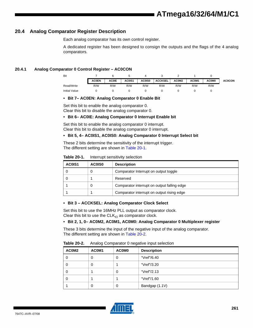
ATmega16/32/64/M1/C1
20.4 Analog Comparator Register DescriptionEach analog comparator has its own control register.
A dedicated register has been designed to consign the outputs and the flags of the 4 analogcomparators.
20.4.1 Analog Comparator 0 Control Register – AC0CON
• Bit 7– AC0EN: Analog Comparator 0 Enable Bit
Set this bit to enable the analog comparator 0.Clear this bit to disable the analog comparator 0.• Bit 6– AC0IE: Analog Comparator 0 Interrupt Enable bit
Set this bit to enable the analog comparator 0 interrupt.Clear this bit to disable the analog comparator 0 interrupt.• Bit 5, 4– AC0IS1, AC0IS0: Analog Comparator 0 Interrupt Select bit
These 2 bits determine the sensitivity of the interrupt trigger.The different setting are shown in Table 20-1.
• Bit 3 – ACCKSEL: Analog Comparator Clock Select
Set this bit to use the 16MHz PLL output as comparator clock.Clear this bit to use the CLKIO as comparator clock.• Bit 2, 1, 0– AC0M2, AC0M1, AC0M0: Analog Comparator 0 Multiplexer register
These 3 bits determine the input of the negative input of the analog comparator.The different setting are shown in Table 20-2.
Bit 7 6 5 4 3 2 1 0
AC0EN AC0IE AC0IS1 AC0IS0 ACCKSEL AC0M2 AC0M1 AC0M0 AC0CON
Read/Write R/W R/W R/W R/W R/W R/W R/W R/W
Initial Value 0 0 0 0 0 0 0 0
Table 20-1. Interrupt sensitivity selection
AC0IS1 AC0IS0 Description
0 0 Comparator Interrupt on output toggle
0 1 Reserved
1 0 Comparator interrupt on output falling edge
1 1 Comparator interrupt on output rising edge
Table 20-2. Analog Comparator 0 negative input selection
AC0M2 AC0M1 AC0M0 Description
0 0 0 “Vref”/6.40
0 0 1 “Vref”/3.20
0 1 0 “Vref”/2.13
0 1 1 “Vref”/1.60
1 0 0 Bandgap (1.1V)
2617647C–AVR–07/08

20.4.2 Analog Comparator 1Control Register – AC1CON
• Bit 7– AC1EN: Analog Comparator 1 Enable Bit
Set this bit to enable the analog comparator 1.Clear this bit to disable the analog comparator 1.• Bit 6– AC1IE: Analog Comparator 1 Interrupt Enable bit
Set this bit to enable the analog comparator 1 interrupt.Clear this bit to disable the analog comparator 1 interrupt.• Bit 5, 4– AC1IS1, AC1IS0: Analog Comparator 1 Interrupt Select bit
These 2 bits determine the sensitivity of the interrupt trigger.The different setting are shown in Table 20-1.
• Bit 3– AC1ICE: Analog Comparator 1 Interrupt Capture Enable bit
Set this bit to enable the input capture of the Timer/Counter1 on the analog comparator event.The comparator output is in this case directly connected to the input capture front-end logic,making the comparator uti l ize the noise canceler and edge select features of theTimer/Counter1 Input Capture interrupt. To make the comparator trigger the Timer/Counter1Input Capture interrupt, the ICIE1 bit in the Timer Interrupt Mask Register (TIMSK1) must be set.
In case ICES1 bit (“Timer/Counter1 Control Register B – TCCR1B” on page 130) is set high, therising edge of AC1O is the capture/trigger event of the Timer/Counter1, in case ICES1 is set tozero, it is the falling edge which is taken into account.
Clear this bit to disable this function. In this case, no connection between the Analog Compara-tor and the input capture function exists.• Bit 2, 1, 0– AC1M2, AC1M1, AC1M0: Analog Comparator 1 Multiplexer register
1 0 1 DAC result
1 1 0 Analog Comparator Negative Input (ACMPM pin)
1 1 1 Reserved
Table 20-2. Analog Comparator 0 negative input selection
AC0M2 AC0M1 AC0M0 Description
Bit 7 6 5 4 3 2 1 0
AC1EN AC1IE AC1IS1 AC1IS0 AC1ICE AC1M2 AC1M1 AC1M0 AC1CON
Read/Write R/W R/W R/W R/W R/W R/W R/W R/W
Initial Value 0 0 0 0 0 0 0 0
Table 20-3. Interrupt sensitivity selection
AC1IS1 AC1IS0 Description
0 0 Comparator Interrupt on output toggle
0 1 Reserved
1 0 Comparator interrupt on output falling edge
1 1 Comparator interrupt on output rising edge
2627647C–AVR–07/08
ATmega16/32/64/M1/C1

ATmega16/32/64/M1/C1
These 3 bits determine the input of the negative input of the analog comparator.The different setting are shown in Table 20-4.
20.4.3 Analog Comparator 2 Control Register – AC2CON
• Bit 7– AC2EN: Analog Comparator 2 Enable Bit
Set this bit to enable the analog comparator 2.Clear this bit to disable the analog comparator 2.• Bit 6– AC2IE: Analog Comparator 2 Interrupt Enable bit
Set this bit to enable the analog comparator 2 interrupt.Clear this bit to disable the analog comparator 2 interrupt. • Bit 5, 4– AC2IS1, AC2IS0: Analog Comparator 2 Interrupt Select bit
These 2 bits determine the sensitivity of the interrupt trigger.The different setting are shown in Table 20-1.
• Bit 3 – Res: Reserved Bit
This bit is an unused bit in the ATmega16/32/64/M1/C1, and will always read as zero.• Bit 2, 1, 0– AC2M2, AC2M1, AC2M0: Analog Comparator 2 Multiplexer register
Table 20-4. Analog Comparator 1 negative input selection
AC1M2 AC1M1 AC1M0 Description
0 0 0 “Vref”/6.40
0 0 1 “Vref”/3.20
0 1 0 “Vref”/2.13
0 1 1 “Vref”/1.60
1 0 0 Bandgap (1.1V)
1 0 1 DAC result
1 1 0 Analog Comparator Negative Input (ACMPM pin)
1 1 1 Reserved
Bit 7 6 5 4 3 2 1 0
AC2EN AC2IE AC2IS1 AC2IS0 - AC2M2 AC2M1 AC2M0 AC2CON
Read/Write R/W R/W R/W R/W - R/W R/W R/W
Initial Value 0 0 0 0 0 0 0 0
Table 20-5. Interrupt sensitivity selection
AC2IS1 AC2IS0 Description
0 0 Comparator Interrupt on output toggle
0 1 Reserved
1 0 Comparator interrupt on output falling edge
1 1 Comparator interrupt on output rising edge
2637647C–AVR–07/08

These 3 bits determine the input of the negative input of the analog comparator.The different setting are shown in Table 20-6.
20.4.4 Analog Comparator 3 Control Register – AC3CON
• Bit 7– AC3EN: Analog Comparator 3 Enable Bit
Set this bit to enable the analog comparator 3.Clear this bit to disable the analog comparator 3.• Bit 6– AC3IE: Analog Comparator 3 Interrupt Enable bit
Set this bit to enable the analog comparator 3 interrupt.Clear this bit to disable the analog comparator 3 interrupt. • Bit 5, 4– AC3IS1, AC3IS0: Analog Comparator 3 Interrupt Select bit
These 2 bits determine the sensitivity of the interrupt trigger.The different setting are shown in Table 20-1.
• Bit 3 – Res: Reserved Bit
This bit is an unused bit in the ATmega16/32/64/M1/C1, and will always read as zero.• Bit 2, 1, 0– AC3M2, AC3M1, AC3M0: Analog Comparator 3 Multiplexer register
Table 20-6. Analog Comparator 2 negative input selection
AC2M2 AC2M1 AC2M0 Description
0 0 0 “Vref”/6.40
0 0 1 “Vref”/3.20
0 1 0 “Vref”/2.13
0 1 1 “Vref”/1.60
1 0 0 Bandgap (1.1V)
1 0 1 DAC result
1 1 0 Analog Comparator Negative Input (ACMPM pin)
1 1 1 Reserved
Bit 7 6 5 4 3 2 1 0
AC3EN AC3IE AC3IS1 AC3IS0 - AC3M2 AC3M1 AC3M0 AC3CON
Read/Write R/W R/W R/W R/W - R/W R/W R/W
Initial Value 0 0 0 0 0 0 0 0
Table 20-7. Interrupt sensitivity selection
AC3IS1 AC3IS0 Description
0 0 Comparator Interrupt on output toggle
0 1 Reserved
1 0 Comparator interrupt on output falling edge
1 1 Comparator interrupt on output rising edge
2647647C–AVR–07/08
ATmega16/32/64/M1/C1

ATmega16/32/64/M1/C1
These 3 bits determine the input of the negative input of the analog comparator.The different setting are shown in Table 20-6.
20.4.5 Analog Comparator Status Register – ACSR
• Bit 7– AC3IF: Analog Comparator 3 Interrupt Flag Bit
This bit is set by hardware when comparator 3 output event triggers off the interrupt modedefined by AC3IS1 and AC3IS0 bits in AC2CON register.This bit is cleared by hardware when the corresponding interrupt vector is executed in case theAC3IE in AC3CON register is set. Anyway, this bit is cleared by writing a logical one on it.This bit can also be used to synchronize ADC or DAC conversions.• Bit 6– AC2IF: Analog Comparator 2 Interrupt Flag Bit
This bit is set by hardware when comparator 2 output event triggers off the interrupt modedefined by AC2IS1 and AC2IS0 bits in AC2CON register.This bit is cleared by hardware when the corresponding interrupt vector is executed in case theAC2IE in AC2CON register is set. Anyway, this bit is cleared by writing a logical one on it.This bit can also be used to synchronize ADC or DAC conversions.• Bit 5– AC1IF: Analog Comparator 1 Interrupt Flag Bit
This bit is set by hardware when comparator 1 output event triggers off the interrupt modedefined by AC1IS1 and AC1IS0 bits in AC1CON register.This bit is cleared by hardware when the corresponding interrupt vector is executed in case theAC1IE in AC1CON register is set. Anyway, this bit is cleared by writing a logical one on it.This bit can also be used to synchronize ADC or DAC conversions.• Bit 4– AC0IF: Analog Comparator 0 Interrupt Flag Bit
This bit is set by hardware when comparator 0 output event triggers off the interrupt modedefined by AC0IS1 and AC0IS0 bits in AC0CON register.This bit is cleared by hardware when the corresponding interrupt vector is executed in case theAC0IE in AC0CON register is set. Anyway, this bit is cleared by writing a logical one on it.This bit can also be used to synchronize ADC or DAC conversions.• Bit 3– AC3O: Analog Comparator 3 Output Bit
Table 20-8. Analog Comparator 3 negative input selection
AC3M2 AC3M1 AC3M0 Description
0 0 0 “Vref”/6.40
0 0 1 “Vref”/3.20
0 1 0 “Vref”/2.13
0 1 1 “Vref”/1.60
1 0 0 Bandgap (1.1V)
1 0 1 DAC result
1 1 0 Analog Comparator Negative Input (ACMPM pin)
1 1 1 Reserved
Bit 7 6 5 4 3 2 1 0
AC3IF AC2IF AC1IF AC0IF AC3O AC2O AC1O AC0O ACSR
Read/Write R/W R/W R/W R/W R R R R
Initial Value 0 0 0 0 0 0 0 0
2657647C–AVR–07/08

AC3O bit is directly the output of the Analog comparator 2.Set when the output of the comparator is high.Cleared when the output comparator is low.• Bit 2– AC2O: Analog Comparator 2 Output Bit
AC2O bit is directly the output of the Analog comparator 2.Set when the output of the comparator is high.Cleared when the output comparator is low.• Bit 1– AC1O: Analog Comparator 1 Output Bit
AC1O bit is directly the output of the Analog comparator 1.Set when the output of the comparator is high.Cleared when the output comparator is low.• Bit 0– AC0O: Analog Comparator 0 Output Bit
AC0O bit is directly the output of the Analog comparator 0.Set when the output of the comparator is high.Cleared when the output comparator is low.
20.4.6 Digital Input Disable Register 0 – DIDR0
• Bit 6, 5, 3, 2, 0 – ACMPN1D, ACMPN0D, ACMPN2D, ACMP2D and ACMPN3D:ACMPN1, ACMPN0, ACMPN2, ACMP2 and ACMPN3 Digital Input Disable
When this bit is written logic one, the digital input buffer on the corresponding Analog pin is dis-abled. The corresponding PIN Register bit will always read as zero when this bit is set. When ananalog signal is applied to one of these pins and the digital input from this pin is not needed, thisbit should be written logic one to reduce power consumption in the digital input buffer.
20.4.7 Digital Input Disable Register 1– DIDR1
• Bit 5, 2, 1: ACMP0D, ACMP1PD, ACMP3PD:ACMP0, ACMP1P, ACMP3P Digital Input Disable
When this bit is written logic one, the digital input buffer on the corresponding analog pin is dis-abled. The corresponding PIN Register bit will always read as zero when this bit is set. When ananalog signal is applied to one of these pins and the digital input from this pin is not needed, thisbit should be written logic one to reduce power consumption in the digital input buffer.
Bit 7 6 5 4 3 2 1 0
ADC7D ADC6DACMPN1DAMP2ND
ADC5DACMPN0D
ADC4D ADC3DACMPN2D
ADC2DACMP2D
ADC1D ADC0DACMPN3D
DIDR0
Read/Write R/W R/W R/W R/W R/W R/W R/W R/W
Initial Value 0 0 0 0 0 0 0 0
Bit 7 6 5 4 3 2 1 0
- AMP2PD ACMP0D AMP0PD AMP0ND ADC10DACMP1D
ADC9DAMP1PDACMP3D
ADC8DAMP1ND
DIDR1
Read/Write - - R/W R/W R/W R/W R/W R/W
Initial Value 0 0 0 0 0 0 0 0
2667647C–AVR–07/08
ATmega16/32/64/M1/C1

ATmega16/32/64/M1/C1
21. Digital to Analog Converter - DAC
21.1 Features• 10 bits resolution• 8 bits linearity• +/- 0.5 LSB accuracy between 150mV and AVcc-150mV• Vout = DAC*Vref/1023• The DAC could be connected to the negative inputs of the analog comparators and/or to a
dedicated output driver.• The output impedance of the driver is around 100 Ohms. So the driver is able to load a 1nF
capacitance in parallel with a resistor higher than 33K with a time constant around 1us.
The ATmega16/32/64/M1/C1 features a 10-bit Digital to Analog Converter. This DAC can beused for the analog comparators and/or can be output on the D2A pin of the microcontroller viaa dedicated driver.
The DAC has a separate analog supply voltage pin, AVCC. AVCC must not differ more than ±0.3V from VCC. See the paragraph “ADC Noise Canceler” on page 234 on how to connect thispin.
The reference voltage is the same as the one used for the ADC, See “ADC Multiplexer Register– ADMUX” on page 242.. These nominally 2.56V Vref or AVCC are provided On-chip. The volt-age reference may be externally decoupled at the AREF pin by a capacitor for better noiseperformance.
2677647C–AVR–07/08

Figure 21-1. Digital to Analog Converter Block Schematic
21.2 OperationThe Digital to Analog Converter generates an analog signal proportional to the value of the DACregisters value.
In order to have an accurate sampling frequency control, there is the possibility to update theDAC input values through different trigger events.
21.3 Starting a ConversionThe DAC is configured thanks to the DACON register. As soon as the DAEN bit in DACON reg-ister is set, the DAC converts the value present on the DACH and DACL registers in accordancewith the register DACON setting.
Alternatively, a conversion can be triggered automatically by various sources. Auto Triggering isenabled by setting the DAC Auto Trigger Enable bit, DAATE in DACON. The trigger source isselected by setting the DAC Trigger Select bits, DATS in DACON (See description of the DATSbits for a list of the trigger sources). When a positive edge occurs on the selected trigger signal,the DAC converts the value present on the DACH and DACL registers in accordance with theregister DACON setting. This provides a method of starting conversions at fixed intervals. If thetrigger signal is still set when the conversion completes, a new conversion will not be started. Ifanother positive edge occurs on the trigger signal during conversion, the edge will be ignored.Note that an interrupt flag will be set even if the specific interrupt is disabled or the Global Inter-
DAC OutputDriver
DALA DAOE DAEN-DAATE DATS2 DATS1 DATS0
10
DACH DACL
DACON
1010
1 0
VRefD2A pin
DACResult
Update DACTrigger
DAC Low bitsDAC High bits
Edge Detector
Sou
rces
2687647C–AVR–07/08
ATmega16/32/64/M1/C1

ATmega16/32/64/M1/C1
rupt Enable bit in SREG is cleared. A conversion can thus be triggered without causing aninterrupt. However, the interrupt flag must be cleared in order to trigger a new conversion at thenext interrupt event.
21.3.1 DAC Voltage Reference
The reference voltage for the ADC (VREF) indicates the conversion range for the DAC. VREF canbe selected as either AVCC, internal 2.56V reference, or external AREF pin.
AVCC is connected to the DAC through a passive switch. The internal 2.56V reference is gener-ated from the internal bandgap reference (VBG) through an internal amplifier. In either case, theexternal AREF pin is directly connected to the DAC, and the reference voltage can be mademore immune to noise by connecting a capacitor between the AREF pin and ground. VREF canalso be measured at the AREF pin with a high impedant voltmeter. Note that VREF is a highimpedant source, and only a capacitive load should be connected in a system.
If the user has a fixed voltage source connected to the AREF pin, the user may not use the otherreference voltage options in the application, as they will be shorted to the external voltage. If noexternal voltage is applied to the AREF pin, the user may switch between AVCC and 2.56V asreference selection. The first DAC conversion result after switching reference voltage sourcemay be inaccurate, and the user is advised to discard this result.
21.4 DAC Register DescriptionThe DAC is controlled via three dedicated registers:• The DACON register which is used for DAC configuration• DACH and DACL which are used to set the value to be converted.
21.4.1 Digital to Analog Conversion Control Register – DACON
• Bit 7 – DAATE: DAC Auto Trigger Enable bit
Set this bit to update the DAC input value on the positive edge of the trigger signal selected withthe DACTS2-0 bit in DACON register.Clear it to automatically update the DAC input when a value is written on DACH register.• Bit 6:4 – DATS2, DATS1, DATS0: DAC Trigger Selection bits
These bits are only necessary in case the DAC works in auto trigger mode. It means if DAATEbit is set.
In accordance with the Table 1, these 3 bits select the interrupt event which will generate theupdate of the DAC input values. The update will be generated by the rising edge of the selectedinterrupt flag whether the interrupt is enabled or not.
Bit 7 6 5 4 3 2 1 0
DAATE DATS2 DATS1 DATS0 - DALA DAOE DAEN DACONRead/Write R/W R/W R/W R/W - R/W R/W R/W
Initial Value 0 0 0 0 0 0 0 0
Table 1. DAC Auto Trigger source selection
DATS2 DATS1 DATS0 Description
0 0 0 Analog comparator 0
0 0 1 Analog comparator 1
0 1 0 External Interrupt Request 0
0 1 1 Timer/Counter0 Compare Match
2697647C–AVR–07/08

• Bit 2 – DALA: Digital to Analog Left Adjust
Set this bit to left adjust the DAC input data.Clear it to right adjust the DAC input data.The DALA bit affects the configuration of the DAC data registers. Changing this bit affects theDAC output on the next DACH writing.• Bit 1 – DAOE: Digital to Analog Output Enable bit
Set this bit to output the conversion result on D2A,Clear it to use the DAC internally. • Bit 0 – DAEN: Digital to Analog Enable bit
Set this bit to enable the DAC,Clear it to disable the DAC.
21.4.2 Digital to Analog Converter input Register – DACH and DACL
DACH and DACL registers contain the value to be converted into analog voltage.
Writing the DACL register prohibits the update of the input value until DACH has not been writ-ten too. So the normal way to write a 10-bit value in the DAC register is firstly to write DACL theDACH.
In order to work easily with only 8 bits, there is the possibility to left adjust the input value. Likethis it is sufficient to write DACH to update the DAC value.
21.4.2.1 DALA = 0
21.4.2.2 DALA = 1
1 0 0 Timer/Counter0 Overflow
1 0 1 Timer/Counter1 Compare Match B
1 1 0 Timer/Counter1 Overflow
1 1 1 Timer/Counter1 Capture Event
Table 1. DAC Auto Trigger source selection (Continued)
DATS2 DATS1 DATS0 Description
Bit 7 6 5 4 3 2 1 0
- - - - - - DAC9 DAC8 DACHDAC7 DAC6 DAC5 DAC4 DAC3 DAC2 DAC1 DAC0 DACL
Read/Write R/W R/W R/W R/W R/W R/W R/W R/W
R/W R/W R/W R/W R/W R/W R/W R/W
Initial Value 0 0 0 0 0 0 0 0
0 0 0 0 0 0 0 0
Bit 7 6 5 4 3 2 1 0
DAC9 DAC8 DAC7 DAC6 DAC5 DAC4 DAC3 DAC2 DACHDAC1 DAC0 - - - - - - DACL
Read/Write R/W R/W R/W R/W R/W R/W R/W R/W
R/W R/W R/W R/W R/W R/W R/W R/W
Initial Value 0 0 0 0 0 0 0 0
0 0 0 0 0 0 0 0
2707647C–AVR–07/08
ATmega16/32/64/M1/C1

ATmega16/32/64/M1/C1
To work with the 10-bit DAC, two registers have to be updated. In order to avoid intermediatevalue, the DAC input values which are really converted into analog signal are buffered intounreachable registers. In normal mode, the update of the shadow register is done when the reg-ister DACH is written.
In case DAATE bit is set, the DAC input values will be updated on the trigger event selectedthrough DATS bits.In order to avoid wrong DAC input values, the update can only be done after having writtenrespectively DACL and DACH registers. It is possible to work on 8-bit configuration by only writ-ing the DACH value. In this case, update is done each trigger event.
In case DAATE bit is cleared, the DAC is in an automatic update mode. Writing the DACH regis-ter automatically update the DAC input values with the DACH and DACL register values.
It means that whatever is the configuration of the DAATE bit, changing the DACL register has noeffect on the DAC output until the DACH register has also been updated. So, to work with 10bits, DACL must be written first before DACH. To work with 8-bit configuration, writing DACHallows the update of the DAC.
2717647C–AVR–07/08

22. Analog Feature Considerations
22.1 PurposeThe ATmega16/32/64/M1/C1 features several analog features such as ADC, DAC, Amplifiers,Comparators...
The purpose of this chapter is to describe the interaction between these features. This chapterexplains how to set the specific registers to get the system running.
Particularly the different peripheral clocks can interfere together, so special care has to beconsidered.
22.2 Use of an Amplifier as Comparator InputThe internal amplifiers provide differential amplification for ADC converter. To allow signed resultwith the ADC, the output level of the amplifiers is shifted up with a Vref/2 voltage.
For this reason, when used with a comparator, a Vref/2 voltage is added to the voltage of theamplifier outputs.
Figure 22-1. Amplifier and Comparator
The amplifier Clock comes from the ADC and is equal to the ADC Clock divided by 8.
22.3 Use of an Amplifier as Comparator Input and ADC InputThe amplifier can be used as ADC input while it is used as comparator input. In that case, eachtime the amplifier is selected as ADC input, the sampling and hold circuit of the ADC loads theamplifier output. It results a decrease of the amplifier output voltage which can toggle the com-parator output.
+
-
ACMPx
ACxEN
AMPx+
-
AMPCMPx
Analog ComparatorNegative Input
Analog ComparatorOutputAMPx+
AMPx-
ComparatorClock
AmplifierClock
2727647C–AVR–07/08
ATmega16/32/64/M1/C1

ATmega16/32/64/M1/C1
Figure 22-2. Amplifier, Comparator and ADC
22.4 Analog Peripheral Clock Sources
22.4.1 ADC ClockThe ADC clock comes from the clock system (CLKio) and it is divided by the ADC Prescaler.See “ADC Prescaler Selection” on page 244. The bits described in the ADC Prescaler Selectiondetermine the division factor between the system clock frequency and input clock of the ADC.
See “Prescaling and Conversion Timing” on page 230. for a complete description of the ADCclock system.
22.4.2 Comparator ClockWhile it is not connected to an amplifier, a comparator is clocked by the comparator clock whichis configured thanks to the ACCKSEL bit in AC0CON register See “Analog Comparator 0 Con-trol Register – AC0CON” on page 261. One can select between the 16MHz PLL output and theCLKio.
When it is connected to an amplifier, a comparator is clock by twice the amplifier clock.
22.4.3 Amplifier ClockWhen the Amplifier uses the ADC clock, this clock is divided by 8. This insures a maximum fre-quency of 250kHz for the amplifier when the ADC clock is 2MHz. When the ADC is clocked witha frequency higher than 2MHz the amplifier cannot be clocked by the ADC clock.
See “Amplifier” on page 247. for a complete description of the Amplifier clock system.
+
-
ACMPx
ACxEN
AMPx+
-
AMPCMPx
Analog ComparatorNegative Input
Analog ComparatorOutputAMPx+
AMPx-
ComparatorClock
AmplifierClock
ADCSampling& Hold
ADC Multiplexer
2737647C–AVR–07/08

23. debugWIRE On-chip Debug System
23.1 Features• Complete Program Flow Control• Emulates All On-chip Functions, Both Digital and Analog, except RESET Pin• Real-time Operation• Symbolic Debugging Support (Both at C and Assembler Source Level, or for Other HLLs)• Unlimited Number of Program Break Points (Using Software Break Points)• Non-intrusive Operation• Electrical Characteristics Identical to Real Device• Automatic Configuration System• High-Speed Operation• Programming of Non-volatile Memories
23.2 OverviewThe debugWIRE On-chip debug system uses a One-wire, bi-directional interface to control theprogram flow, execute AVR instructions in the CPU and to program the different non-volatilememories.
23.3 Physical InterfaceWhen the debugWIRE Enable (DWEN) Fuse is programmed and Lock bits are unprogrammed,the debugWIRE system within the target device is activated. The RESET port pin is configuredas a wire-AND (open-drain) bi-directional I/O pin with pull-up enabled and becomes the commu-nication gateway between target and emulator.
Figure 23-1. The debugWIRE Setup
Figure 23-1 shows the schematic of a target MCU, with debugWIRE enabled, and the emulatorconnector. The system clock is not affected by debugWIRE and will always be the clock sourceselected by the CKSEL Fuses.
When designing a system where debugWIRE will be used, the following observations must bemade for correct operation:
dW
GND
dW(RESET)
VCC
1.8 - 5.5V
2747647C–AVR–07/08
ATmega16/32/64/M1/C1

ATmega16/32/64/M1/C1
• Pull-up resistors on the dW/(RESET) line must not be smaller than 10kΩ. The pull-up resistor is not required for debugWIRE functionality.
• Connecting the RESET pin directly to VCC will not work.• Capacitors connected to the RESET pin must be disconnected when using debugWire.• All external reset sources must be disconnected.
23.4 Software Break PointsdebugWIRE supports Program memory Break Points by the AVR Break instruction. Setting aBreak Point in AVR Studio® will insert a BREAK instruction in the Program memory. The instruc-tion replaced by the BREAK instruction will be stored. When program execution is continued, thestored instruction will be executed before continuing from the Program memory. A break can beinserted manually by putting the BREAK instruction in the program.
The Flash must be re-programmed each time a Break Point is changed. This is automaticallyhandled by AVR Studio through the debugWIRE interface. The use of Break Points will thereforereduce the Flash Data retention. Devices used for debugging purposes should not be shipped toend customers.
23.5 Limitations of debugWIREThe debugWIRE communication pin (dW) is physically located on the same pin as ExternalReset (RESET). An External Reset source is therefore not supported when the debugWIRE isenabled.
The debugWIRE system accurately emulates all I/O functions when running at full speed, i.e.,when the program in the CPU is running. When the CPU is stopped, care must be taken whileaccessing some of the I/O Registers via the debugger (AVR Studio).
A programmed DWEN Fuse enables some parts of the clock system to be running in all sleepmodes. This will increase the power consumption while in sleep. Thus, the DWEN Fuse shouldbe disabled when debugWire is not used.
23.6 debugWIRE Related Register in I/O Memory The following section describes the registers used with the debugWire.
23.6.1 debugWire Data Register – DWDR
The DWDR Register provides a communication channel from the running program in the MCUto the debugger. This register is only accessible by the debugWIRE and can therefore not beused as a general purpose register in the normal operations.
24. Boot Loader Support – Read-While-Write Self-Programming ATmega16/32/64/M1/C1
In ATmega16/32/64/M1/C1, the Boot Loader Support provides a real Read-While-Write Self-Programming mechanism for downloading and uploading program code by the MCU itself. Thisfeature allows flexible application software updates controlled by the MCU using a Flash-resi-
Bit 7 6 5 4 3 2 1 0
DWDR[7:0] DWDRRead/Write R/W R/W R/W R/W R/W R/W R/W R/W
Initial Value 0 0 0 0 0 0 0 0
2757647C–AVR–07/08

dent Boot Loader program. The Boot Loader program can use any available data interface andassociated protocol to read code and write (program) that code into the Flash memory, or readthe code from the program memory. The program code within the Boot Loader section has thecapability to write into the entire Flash, including the Boot Loader memory. The Boot Loader canthus even modify itself, and it can also erase itself from the code if the feature is not needed any-more. The size of the Boot Loader memory is configurable with fuses and the Boot Loader hastwo separate sets of Boot Lock bits which can be set independently. This gives the user aunique flexibility to select different levels of protection.
24.1 Boot Loader Features• Read-While-Write Self-Programming• Flexible Boot Memory Size• High Security (Separate Boot Lock Bits for a Flexible Protection)• Separate Fuse to Select Reset Vector• Optimized Page(1) Size• Code Efficient Algorithm• Efficient Read-Modify-Write SupportNote: 1. A page is a section in the Flash consisting of several bytes (see Table 25-12 on page 300)
used during programming. The page organization does not affect normal operation.
24.2 Application and Boot Loader Flash SectionsThe Flash memory is organized in two main sections, the Application section and the BootLoader section (see Figure 24-2). The size of the different sections is configured by theBOOTSZ Fuses as shown in Table 24-7 on page 289 and Figure 24-2. These two sections canhave different level of protection since they have different sets of Lock bits.
24.2.1 Application Section
The Application section is the section of the Flash that is used for storing the application code.The protection level for the Application section can be selected by the application Boot Lock bits(Boot Lock bits 0), see Table 24-2 on page 280. The Application section can never store anyBoot Loader code since the SPM instruction is disabled when executed from the Applicationsection.
24.2.2 BLS – Boot Loader Section
While the Application section is used for storing the application code, the The Boot Loader soft-ware must be located in the BLS since the SPM instruction can initiate a programming whenexecuting from the BLS only. The SPM instruction can access the entire Flash, including theBLS itself. The protection level for the Boot Loader section can be selected by the Boot LoaderLock bits (Boot Lock bits 1), see Table 24-3 on page 280.
24.3 Read-While-Write and No Read-While-Write Flash SectionsWhether the CPU supports Read-While-Write or if the CPU is halted during a Boot Loader soft-ware update is dependent on which address that is being programmed. In addition to the twosections that are configurable by the BOOTSZ Fuses as described above, the Flash is alsodivided into two fixed sections, the Read-While-Write (RWW) section and the No Read-While-Write (NRWW) section. The limit between the RWW- and NRWW sections is given in Table 24-8 on page 289 and Figure 24-2 on page 279. The main difference between the two sections is:• When erasing or writing a page located inside the RWW section, the NRWW section can be
read during the operation.• When erasing or writing a page located inside the NRWW section, the CPU is halted during
the entire operation.
2767647C–AVR–07/08
ATmega16/32/64/M1/C1

ATmega16/32/64/M1/C1
Note that the user software can never read any code that is located inside the RWW section dur-ing a Boot Loader software operation. The syntax “Read-While-Write section” refers to whichsection that is being programmed (erased or written), not which section that actually is beingread during a Boot Loader software update.
24.3.1 RWW – Read-While-Write Section
If a Boot Loader software update is programming a page inside the RWW section, it is possibleto read code from the Flash, but only code that is located in the NRWW section. During an on-going programming, the software must ensure that the RWW section never is being read. If theuser software is trying to read code that is located inside the RWW section (i.e., by acall/jmp/lpm or an interrupt) during programming, the software might end up in an unknownstate. To avoid this, the interrupts should either be disabled or moved to the Boot Loader sec-tion. The Boot Loader section is always located in the NRWW section. The RWW Section Busybit (RWWSB) in the Store Program Memory Control and Status Register (SPMCSR) will be readas logical one as long as the RWW section is blocked for reading. After a programming is com-pleted, the RWWSB must be cleared by software before reading code located in the RWWsection. See “Store Program Memory Control and Status Register – SPMCSR” on page 281. fordetails on how to clear RWWSB.
24.3.2 NRWW – No Read-While-Write Section
The code located in the NRWW section can be read when the Boot Loader software is updatinga page in the RWW section. When the Boot Loader code updates the NRWW section, the CPUis halted during the entire Page Erase or Page Write operation.
Table 24-1. Read-While-Write Features
Which Section does the Z-pointer Address During the Programming?
Which Section Can be Read During Programming?
Is the CPU Halted?
Read-While-Write Supported?
RWW Section NRWW Section No Yes
NRWW Section None Yes No
2777647C–AVR–07/08
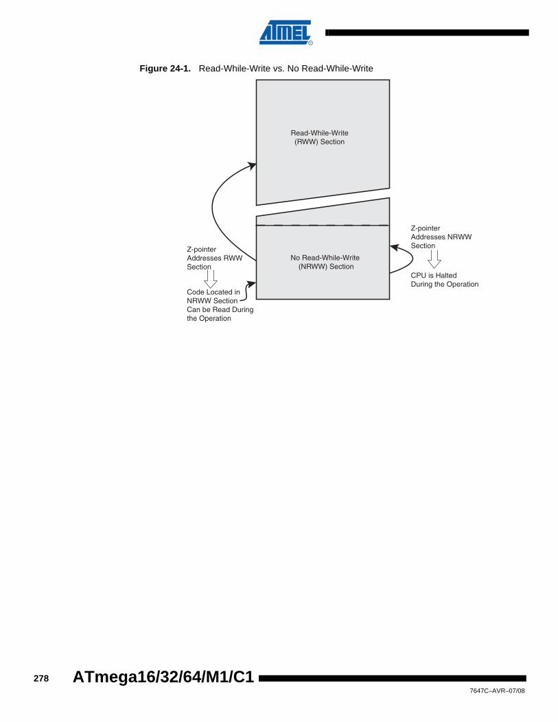
Figure 24-1. Read-While-Write vs. No Read-While-Write
Read-While-Write(RWW) Section
No Read-While-Write (NRWW) Section
Z-pointerAddresses RWWSection
Z-pointerAddresses NRWWSection
CPU is HaltedDuring the Operation
Code Located in NRWW SectionCan be Read Duringthe Operation
2787647C–AVR–07/08
ATmega16/32/64/M1/C1

ATmega16/32/64/M1/C1
Figure 24-2. Memory Sections
Note: 1. The parameters in the figure above are given in Table 24-7 on page 289.
24.4 Boot Loader Lock BitsIf no Boot Loader capability is needed, the entire Flash is available for application code. TheBoot Loader has two separate sets of Boot Lock bits which can be set independently. This givesthe user a unique flexibility to select different levels of protection.
The user can select:• To protect the entire Flash from a software update by the MCU.• To protect only the Boot Loader Flash section from a software update by the MCU.• To protect only the Application Flash section from a software update by the MCU.• Allow software update in the entire Flash.
See Table 24-2 and Table 24-3 for further details. The Boot Lock bits can be set in software andin Serial or Parallel Programming mode, but they can be cleared by a Chip Erase commandonly. The general Write Lock (Lock Bit mode 2) does not control the programming of the Flashmemory by SPM instruction. Similarly, the general Read/Write Lock (Lock Bit mode 1) does notcontrol reading nor writing by LPM/SPM, if it is attempted.
0x0000
Flashend
Program MemoryBOOTSZ = '11'
Application Flash Section
Boot Loader Flash SectionFlashend
Program MemoryBOOTSZ = '10'
0x0000
Program MemoryBOOTSZ = '01'
Program MemoryBOOTSZ = '00'
Application Flash Section
Boot Loader Flash Section
0x0000
Flashend
Application Flash Section
Flashend
End RWW
Start NRWW
Application Flash Section
Boot Loader Flash Section
Boot Loader Flash Section
End RWW
Start NRWW
End RWW
Start NRWW
0x0000
End RWW, End Application
Start NRWW, Start Boot Loader
Application Flash SectionApplication Flash Section
Application Flash Section
Rea
d-W
hile
-Writ
e S
ectio
nN
o R
ead-
Whi
le-W
rite
Sec
tion
Rea
d-W
hile
-Writ
e S
ectio
nN
o R
ead-
Whi
le-W
rite
Sec
tion
Rea
d-W
hile
-Writ
e S
ectio
nN
o R
ead-
Whi
le-W
rite
Sec
tion
Rea
d-W
hile
-Writ
e S
ectio
nN
o R
ead-
Whi
le-W
rite
Sec
tion
End Application
Start Boot Loader
End Application
Start Boot Loader
End Application
Start Boot Loader
2797647C–AVR–07/08
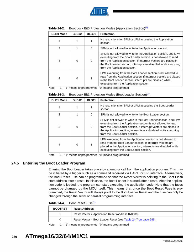
Note: 1. “1” means unprogrammed, “0” means programmed
Note: 1. “1” means unprogrammed, “0” means programmed
24.5 Entering the Boot Loader ProgramEntering the Boot Loader takes place by a jump or call from the application program. This maybe initiated by a trigger such as a command received via UART, or SPI interface. Alternatively,the Boot Reset Fuse can be programmed so that the Reset Vector is pointing to the Boot Flashstart address after a reset. In this case, the Boot Loader is started after a reset. After the applica-tion code is loaded, the program can start executing the application code. Note that the fusescannot be changed by the MCU itself. This means that once the Boot Reset Fuse is pro-grammed, the Reset Vector will always point to the Boot Loader Reset and the fuse can only bechanged through the serial or parallel programming interface.
Note: 1. “1” means unprogrammed, “0” means programmed
Table 24-2. Boot Lock Bit0 Protection Modes (Application Section)(1)
BLB0 Mode BLB02 BLB01 Protection
1 1 1 No restrictions for SPM or LPM accessing the Application section.
2 1 0 SPM is not allowed to write to the Application section.
3 0 0
SPM is not allowed to write to the Application section, and LPM executing from the Boot Loader section is not allowed to read from the Application section. If Interrupt Vectors are placed in the Boot Loader section, interrupts are disabled while executing from the Application section.
4 0 1
LPM executing from the Boot Loader section is not allowed to read from the Application section. If Interrupt Vectors are placed in the Boot Loader section, interrupts are disabled while executing from the Application section.
Table 24-3. Boot Lock Bit1 Protection Modes (Boot Loader Section)(1)
BLB1 Mode BLB12 BLB11 Protection
1 1 1 No restrictions for SPM or LPM accessing the Boot Loader section.
2 1 0 SPM is not allowed to write to the Boot Loader section.
3 0 0
SPM is not allowed to write to the Boot Loader section, and LPM executing from the Application section is not allowed to read from the Boot Loader section. If Interrupt Vectors are placed in the Application section, interrupts are disabled while executing from the Boot Loader section.
4 0 1
LPM executing from the Application section is not allowed to read from the Boot Loader section. If Interrupt Vectors are placed in the Application section, interrupts are disabled while executing from the Boot Loader section.
Table 24-4. Boot Reset Fuse(1)
BOOTRST Reset Address
1 Reset Vector = Application Reset (address 0x0000)
0 Reset Vector = Boot Loader Reset (see Table 24-7 on page 289)
2807647C–AVR–07/08
ATmega16/32/64/M1/C1

ATmega16/32/64/M1/C1
24.5.1 Store Program Memory Control and Status Register – SPMCSR
The Store Program Memory Control and Status Register contains the control bits needed to con-trol the Boot Loader operations.
• Bit 7 – SPMIE: SPM Interrupt Enable
When the SPMIE bit is written to one, and the I-bit in the Status Register is set (one), the SPMready interrupt will be enabled. The SPM ready Interrupt will be executed as long as the SPMENbit in the SPMCSR Register is cleared.• Bit 6 – RWWSB: Read-While-Write Section Busy
When a Self-Programming (Page Erase or Page Write) operation to the RWW section is initi-ated, the RWWSB will be set (one) by hardware. When the RWWSB bit is set, the RWW sectioncannot be accessed. The RWWSB bit will be cleared if the RWWSRE bit is written to one after aSelf-Programming operation is completed. Alternatively the RWWSB bit will automatically becleared if a page load operation is initiated.
• Bit 5 – SIGRD: Signature Row ReadIf this bit is written to one at the same time as SPMEN, the next LPM instruction within threeclock cycles will read a byte from the signature row into the destination register. see “Readingthe Signature Row from Software” on page 286 for details. An SPM instruction within four cyclesafter SIGRD and SPMEN are set will have no effect. This operation is reserved for future useand should not be used.
• Bit 4 – RWWSRE: Read-While-Write Section Read Enable
When programming (Page Erase or Page Write) to the RWW section, the RWW section isblocked for reading (the RWWSB will be set by hardware). To re-enable the RWW section, theuser software must wait until the programming is completed (SPMEN will be cleared). Then, ifthe RWWSRE bit is written to one at the same time as SPMEN, the next SPM instruction withinfour clock cycles re-enables the RWW section. The RWW section cannot be re-enabled whilethe Flash is busy with a Page Erase or a Page Write (SPMEN is set). If the RWWSRE bit is writ-ten while the Flash is being loaded, the Flash load operation will abort and the data loaded willbe lost.• Bit 3 – BLBSET: Boot Lock Bit Set
If this bit is written to one at the same time as SPMEN, the next SPM instruction within four clockcycles sets Boot Lock bits and Memory Lock bits, according to the data in R0. The data in R1and the address in the Z-pointer are ignored. The BLBSET bit will automatically be cleared uponcompletion of the Lock bit set, or if no SPM instruction is executed within four clock cycles.
An LPM instruction within three cycles after BLBSET and SPMEN are set in the SPMCSR Reg-ister, will read either the Lock bits or the Fuse bits (depending on Z0 in the Z-pointer) into thedestination register. See “Reading the Fuse and Lock Bits from Software” on page 285 fordetails.• Bit 2 – PGWRT: Page Write
If this bit is written to one at the same time as SPMEN, the next SPM instruction within four clockcycles executes Page Write, with the data stored in the temporary buffer. The page address istaken from the high part of the Z-pointer. The data in R1 and R0 are ignored. The PGWRT bitwill auto-clear upon completion of a Page Write, or if no SPM instruction is executed within four
Bit 7 6 5 4 3 2 1 0
SPMIE RWWSB SIGRD RWWSRE BLBSET PGWRT PGERS SPMEN SPMCSR
Read/Write R/W R R R/W R/W R/W R/W R/W
Initial Value 0 0 0 0 0 0 0 0
2817647C–AVR–07/08

clock cycles. The CPU is halted during the entire Page Write operation if the NRWW section isaddressed.• Bit 1 – PGERS: Page Erase
If this bit is written to one at the same time as SPMEN, the next SPM instruction within four clockcycles executes Page Erase. The page address is taken from the high part of the Z-pointer. Thedata in R1 and R0 are ignored. The PGERS bit will auto-clear upon completion of a Page Erase,or if no SPM instruction is executed within four clock cycles. The CPU is halted during the entirePage Write operation if the NRWW section is addressed.• Bit 0 – SPMEN: Self Programming Enable
This bit enables the SPM instruction for the next four clock cycles. If written to one together witheither RWWSRE, BLBSET, PGWRT or PGERS, the following SPM instruction will have a spe-cial meaning, see description above. If only SPMEN is written, the following SPM instruction willstore the value in R1:R0 in the temporary page buffer addressed by the Z-pointer. The LSB ofthe Z-pointer is ignored. The SPMEN bit will auto-clear upon completion of an SPM instruction,or if no SPM instruction is executed within four clock cycles. During Page Erase and Page Write,the SPMEN bit remains high until the operation is completed.
Writing any other combination than “10001”, “01001”, “00101”, “00011” or “00001” in the lowerfive bits will have no effect.
24.6 Addressing the Flash During Self-ProgrammingThe Z-pointer is used to address the SPM commands.
Since the Flash is organized in pages (see Table 25-12 on page 300), the Program Counter canbe treated as having two different sections. One section, consisting of the least significant bits, isaddressing the words within a page, while the most significant bits are addressing the pages.This is1 shown in Figure 24-3. Note that the Page Erase and Page Write operations areaddressed independently. Therefore it is of major importance that the Boot Loader softwareaddresses the same page in both the Page Erase and Page Write operation. Once a program-ming operation is initiated, the address is latched and the Z-pointer can be used for otheroperations.
The only SPM operation that does not use the Z-pointer is Setting the Boot Loader Lock bits.The content of the Z-pointer is ignored and will have no effect on the operation. The LPMinstruction does also use the Z-pointer to store the address. Since this instruction addresses theFlash byte-by-byte, also the LSB (bit Z0) of the Z-pointer is used.
Bit 15 14 13 12 11 10 9 8
ZH (R31) Z15 Z14 Z13 Z12 Z11 Z10 Z9 Z8ZL (R30) Z7 Z6 Z5 Z4 Z3 Z2 Z1 Z0
7 6 5 4 3 2 1 0
2827647C–AVR–07/08
ATmega16/32/64/M1/C1

ATmega16/32/64/M1/C1
Figure 24-3. Addressing the Flash During SPM(1)
Note: 1. The different variables used in Figure 24-3 are listed in Table 24-9 on page 289.
24.7 Self-Programming the FlashThe program memory is updated in a page by page fashion. Before programming a page withthe data stored in the temporary page buffer, the page must be erased. The temporary pagebuffer is filled one word at a time using SPM and the buffer can be filled either before the PageErase command or between a Page Erase and a Page Write operation:
Alternative 1, fill the buffer before a Page Erase• Fill temporary page buffer• Perform a Page Erase• Perform a Page Write
Alternative 2, fill the buffer after Page Erase• Perform a Page Erase• Fill temporary page buffer• Perform a Page Write
If only a part of the page needs to be changed, the rest of the page must be stored (for examplein the temporary page buffer) before the erase, and then be rewritten. When using alternative 1,the Boot Loader provides an effective Read-Modify-Write feature which allows the user softwareto first read the page, do the necessary changes, and then write back the modified data. If alter-native 2 is used, it is not possible to read the old data while loading since the page is alreadyerased. The temporary page buffer can be accessed in a random sequence. It is essential thatthe page address used in both the Page Erase and Page Write operation is addressing thesame page. See “Simple Assembly Code Example for a Boot Loader” on page 287 for anassembly code example.
PROGRAM MEMORY
0115
Z - REGISTER
BIT
0
ZPAGEMSB
WORD ADDRESSWITHIN A PAGE
PAGE ADDRESSWITHIN THE FLASH
ZPCMSB
INSTRUCTION WORD
PAGE PCWORD[PAGEMSB:0]:
00
01
02
PAGEEND
PAGE
PCWORDPCPAGE
PCMSB PAGEMSBPROGRAMCOUNTER
2837647C–AVR–07/08

24.7.1 Performing Page Erase by SPM
To execute Page Erase, set up the address in the Z-pointer, write “X0000011” to SPMCSR andexecute SPM within four clock cycles after writing SPMCSR. The data in R1 and R0 is ignored.The page address must be written to PCPAGE in the Z-register. Other bits in the Z-pointer willbe ignored during this operation.• Page Erase to the RWW section: The NRWW section can be read during the Page Erase.• Page Erase to the NRWW section: The CPU is halted during the operation.
24.7.2 Filling the Temporary Buffer (Page Loading)
To write an instruction word, set up the address in the Z-pointer and data in R1:R0, write“00000001” to SPMCSR and execute SPM within four clock cycles after writing SPMCSR. Thecontent of PCWORD in the Z-register is used to address the data in the temporary buffer. Thetemporary buffer will auto-erase after a Page Write operation or by writing the RWWSRE bit inSPMCSR. It is also erased after a system reset. Note that it is not possible to write more thanone time to each address without erasing the temporary buffer.
If the EEPROM is written in the middle of an SPM Page Load operation, all data loaded will belost.
24.7.3 Performing a Page Write
To execute Page Write, set up the address in the Z-pointer, write “X0000101” to SPMCSR andexecute SPM within four clock cycles after writing SPMCSR. The data in R1 and R0 is ignored.The page address must be written to PCPAGE. Other bits in the Z-pointer must be written tozero during this operation.• Page Write to the RWW section: The NRWW section can be read during the Page Write.• Page Write to the NRWW section: The CPU is halted during the operation.
24.7.4 Using the SPM Interrupt
If the SPM interrupt is enabled, the SPM interrupt will generate a constant interrupt when theSPMEN bit in SPMCSR is cleared. This means that the interrupt can be used instead of pollingthe SPMCSR Register in software. When using the SPM interrupt, the Interrupt Vectors shouldbe moved to the BLS section to avoid that an interrupt is accessing the RWW section when it isblocked for reading. How to move the interrupts is described in XXXXXXXX.
24.7.5 Consideration While Updating BLS
Special care must be taken if the user allows the Boot Loader section to be updated by leavingBoot Lock bit11 unprogrammed. An accidental write to the Boot Loader itself can corrupt theentire Boot Loader, and further software updates might be impossible. If it is not necessary tochange the Boot Loader software itself, it is recommended to program the Boot Lock bit11 toprotect the Boot Loader software from any internal software changes.
24.7.6 Prevent Reading the RWW Section During Self-Programming
During Self-Programming (either Page Erase or Page Write), the RWW section is alwaysblocked for reading. The user software itself must prevent that this section is addressed duringthe self programming operation. The RWWSB in the SPMCSR will be set as long as the RWWsection is busy. During Self-Programming the Interrupt Vector table should be moved to the BLSas described in XXXXXXX, or the interrupts must be disabled. Before addressing the RWW sec-tion after the programming is completed, the user software must clear the RWWSB by writingthe RWWSRE. See “Simple Assembly Code Example for a Boot Loader” on page 287 for anexample.
2847647C–AVR–07/08
ATmega16/32/64/M1/C1

ATmega16/32/64/M1/C1
24.7.7 Setting the Boot Loader Lock Bits by SPM
To set the Boot Loader Lock bits, write the desired data to R0, write “X0001001” to SPMCSRand execute SPM within four clock cycles after writing SPMCSR. The only accessible Lock bitsare the Boot Lock bits that may prevent the Application and Boot Loader section from any soft-ware update by the MCU.
See Table 24-2 and Table 24-3 for how the different settings of the Boot Loader bits affect theFlash access.
If bits 5..2 in R0 are cleared (zero), the corresponding Boot Lock bit will be programmed if anSPM instruction is executed within four cycles after BLBSET and SPMEN are set in SPMCSR.The Z-pointer is don’t care during this operation, but for future compatibility it is recommended toload the Z-pointer with 0x0001 (same as used for reading the lOck bits). For future compatibility itis also recommended to set bits 7, 6, 1, and 0 in R0 to “1” when writing the Lock bits. When pro-gramming the Lock bits the entire Flash can be read during the operation.
24.7.8 EEPROM Write Prevents Writing to SPMCSR
Note that an EEPROM write operation will block all software programming to Flash. Reading theFuses and Lock bits from software will also be prevented during the EEPROM write operation. Itis recommended that the user checks the status bit (EEWE) in the EECR Register and verifiesthat the bit is cleared before writing to the SPMCSR Register.
24.7.9 Reading the Fuse and Lock Bits from Software
It is possible to read both the Fuse and Lock bits from software. To read the Lock bits, load theZ-pointer with 0x0001 and set the BLBSET and SPMEN bits in SPMCSR. When an LPM instruc-tion is executed within three CPU cycles after the BLBSET and SPMEN bits are set in SPMCSR,the value of the Lock bits will be loaded in the destination register. The BLBSET and SPMENbits will auto-clear upon completion of reading the Lock bits or if no LPM instruction is executedwithin three CPU cycles or no SPM instruction is executed within four CPU cycles. When BLB-SET and SPMEN are cleared, LPM will work as described in the Instruction set Manual.
The algorithm for reading the Fuse Low byte is similar to the one described above for readingthe Lock bits. To read the Fuse Low byte, load the Z-pointer with 0x0000 and set the BLBSETand SPMEN bits in SPMCSR. When an LPM instruction is executed within three cycles after theBLBSET and SPMEN bits are set in the SPMCSR, the value of the Fuse Low byte (FLB) will beloaded in the destination register as shown below. Refer to Table 25-4 on page 295 for adetailed description and mapping of the Fuse Low byte.
Similarly, when reading the Fuse High byte, load 0x0003 in the Z-pointer. When an LPM instruc-tion is executed within three cycles after the BLBSET and SPMEN bits are set in the SPMCSR,the value of the Fuse High byte (FHB) will be loaded in the destination register as shown below.Refer to Table 25-6 on page 297 for detailed description and mapping of the Fuse High byte.
When reading the Extended Fuse byte, load 0x0002 in the Z-pointer. When an LPM instructionis executed within three cycles after the BLBSET and SPMEN bits are set in the SPMCSR, the
Bit 7 6 5 4 3 2 1 0
R0 1 1 BLB12 BLB11 BLB02 BLB01 1 1
Bit 7 6 5 4 3 2 1 0
Rd – – BLB12 BLB11 BLB02 BLB01 LB2 LB1
Bit 7 6 5 4 3 2 1 0
Rd FLB7 FLB6 FLB5 FLB4 FLB3 FLB2 FLB1 FLB0
Bit 7 6 5 4 3 2 1 0
Rd FHB7 FHB6 FHB5 FHB4 FHB3 FHB2 FHB1 FHB0
2857647C–AVR–07/08

value of the Extended Fuse byte (EFB) will be loaded in the destination register as shown below.Refer to Table 25-4 on page 295 for detailed description and mapping of the Extended Fusebyte.
Fuse and Lock bits that are programmed, will be read as zero. Fuse and Lock bits that areunprogrammed, will be read as one.
24.7.10 Reading the Signature Row from SoftwareTo read the Signature Row from software, load the Z-pointer with the signature byte addressgiven in Table 24-5 on page 286 and set the SIGRD and SPMEN bits in SPMCSR. When anLPM instruction is executed within three CPU cycles after the SIGRD and SPMEN bits are set inSPMCSR, the signature byte value will be loaded in the destination register. The SIGRD andSPMEN bits will auto-clear upon completion of reading the Signature Row Lock bits or if no LPMinstruction is executed within three CPU cycles. When SIGRD and SPMEN are cleared, LPM willwork as described in the Instruction set Manual.
Note: All other addresses are reserved for future use.
24.7.11 Preventing Flash Corruption
During periods of low VCC, the Flash program can be corrupted because the supply voltage istoo low for the CPU and the Flash to operate properly. These issues are the same as for boardlevel systems using the Flash, and the same design solutions should be applied.
A Flash program corruption can be caused by two situations when the voltage is too low. First, aregular write sequence to the Flash requires a minimum voltage to operate correctly. Secondly,the CPU itself can execute instructions incorrectly, if the supply voltage for executing instructionsis too low.
Flash corruption can easily be avoided by following these design recommendations (one issufficient):1. If there is no need for a Boot Loader update in the system, program the Boot Loader
Lock bits to prevent any Boot Loader software updates.2. Keep the AVR RESET active (low) during periods of insufficient power supply voltage.
This can be done by enabling the internal Brown-out Detector (BOD) if the operating volt-age matches the detection level. If not, an external low VCC reset protection circuit can beused. If a reset occurs while a write operation is in progress, the write operation will becompleted provided that the power supply voltage is sufficient.
Bit 7 6 5 4 3 2 1 0
Rd – – – – EFB3 EFB2 EFB1 EFB0
Table 24-5. Signature Row Addressing
Signature Byte Z-Pointer Address
Device Signature Byte 1 0x0000
Device Signature Byte 2 0x0002
Device Signature Byte 3 0x0004
RC Oscillator Calibration Byte 0x0001
TSOFFSET Temp Sensor Offset 0x0005
TSGAIN Temp Sensor Gain 0x0007
2867647C–AVR–07/08
ATmega16/32/64/M1/C1

ATmega16/32/64/M1/C1
3. Keep the AVR core in Power-down sleep mode during periods of low VCC. This will pre-vent the CPU from attempting to decode and execute instructions, effectively protectingthe SPMCSR Register and thus the Flash from unintentional writes.
24.7.12 Programming Time for Flash when Using SPM
The calibrated RC Oscillator is used to time Flash accesses. Table 24-6 shows the typical pro-gramming time for Flash accesses from the CPU.
24.7.13 Simple Assembly Code Example for a Boot Loader;-the routine writes one page of data from RAM to Flash; the first data location in RAM is pointed to by the Y pointer; the first data location in Flash is pointed to by the Z-pointer;-error handling is not included;-the routine must be placed inside the Boot space; (at least the Do_spm sub routine). Only code inside NRWW section can; be read during Self-Programming (Page Erase and Page Write).;-registers used: r0, r1, temp1 (r16), temp2 (r17), looplo (r24), ; loophi (r25), spmcrval (r20); storing and restoring of registers is not included in the routine; register usage can be optimized at the expense of code size;-It is assumed that either the interrupt table is moved to the Boot; loader section or that the interrupts are disabled.
.equ PAGESIZEB = PAGESIZE*2 ;PAGESIZEB is page size in BYTES, not words
.org SMALLBOOTSTARTWrite_page:; Page Eraseldi spmcrval, (1<<PGERS) | (1<<SPMEN)call Do_spm
; re-enable the RWW sectionldi spmcrval, (1<<RWWSRE) | (1<<SPMEN)call Do_spm
; transfer data from RAM to Flash page bufferldi looplo, low(PAGESIZEB) ;init loop variableldi loophi, high(PAGESIZEB) ;not required for PAGESIZEB<=256
Wrloop:ld r0, Y+ld r1, Y+ldi spmcrval, (1<<SPMEN)call Do_spmadiw ZH:ZL, 2sbiw loophi:looplo, 2 ;use subi for PAGESIZEB<=256brne Wrloop
; execute Page Writesubi ZL, low(PAGESIZEB) ;restore pointersbci ZH, high(PAGESIZEB) ;not required for PAGESIZEB<=256ldi spmcrval, (1<<PGWRT) | (1<<SPMEN)call Do_spm
Table 24-6. SPM Programming Time
Symbol Min Programming Time Max Programming Time
Flash write (Page Erase, Page Write, and write Lock bits by SPM) 3.7 ms 4.5 ms
2877647C–AVR–07/08

; re-enable the RWW sectionldi spmcrval, (1<<RWWSRE) | (1<<SPMEN)call Do_spm
; read back and check, optionalldi looplo, low(PAGESIZEB) ;init loop variableldi loophi, high(PAGESIZEB) ;not required for PAGESIZEB<=256subi YL, low(PAGESIZEB) ;restore pointersbci YH, high(PAGESIZEB)
Rdloop:lpm r0, Z+ld r1, Y+cpse r0, r1jmp Errorsbiw loophi:looplo, 1 ;use subi for PAGESIZEB<=256brne Rdloop
; return to RWW section; verify that RWW section is safe to read
Return:in temp1, SPMCSRsbrs temp1, RWWSB ; If RWWSB is set, the RWW section is not ready yetret; re-enable the RWW sectionldi spmcrval, (1<<RWWSRE) | (1<<SPMEN)call Do_spmrjmp Return
Do_spm:; check for previous SPM complete
Wait_spm:in temp1, SPMCSRsbrc temp1, SPMENrjmp Wait_spm; input: spmcrval determines SPM action; disable interrupts if enabled, store statusin temp2, SREGcli; check that no EEPROM write access is present
Wait_ee:sbic EECR, EEPErjmp Wait_ee; SPM timed sequenceout SPMCSR, spmcrvalspm; restore SREG (to enable interrupts if originally enabled)out SREG, temp2ret
2887647C–AVR–07/08
ATmega16/32/64/M1/C1

ATmega16/32/64/M1/C1
24.7.14 ATmega16/32/64/M1/C1 - 16K -Flash Boot Loader Parameters
In Table 24-7 through Table 24-9, the parameters used in the description of the self program-ming are given.
Note: 1. The different BOOTSZ Fuse configurations are shown in Figure 24-2.2. 1 word equals 2 bytes.
For details about these two section, see “NRWW – No Read-While-Write Section” on page 277and “RWW – Read-While-Write Section” on page 277
Note: Z15:Z13: always ignoredZ0: should be zero for all SPM commands, byte select for the LPM instruction.
Table 24-7. Boot Size Configuration, ATmega16/32/64/M1/C1 (16K product)
BOOTSZ1 BOOTSZ0Boot Size(2) Pages
ApplicationFlash Section
Boot LoaderFlash Section
EndApplicationSection
Boot Reset Address (Start Boot Loader Section)
1 1 256 words 4 0x0000 -
0x1EFF0x1F00 - 0x1FFF 0x1EFF 0x1F00
1 0 512 words 8 0x0000 -
0x1DFF0x1E00 - 0x1FFF 0x1DFF 0x1E00
0 1 1024 words 16 0x0000 -
0x1BFF0x1C00 - 0x1FFF 0x1BFF 0x1C00
0 0 2048 words 32 0x0000 -
0x17FF0x1800 - 0x1FFF 0x17FF 0x1800
Table 24-8. Read-While-Write Limit
Section Pages Address
Read-While-Write section (RWW) 96 0x0000 - 0x37FF
No Read-While-Write section (NRWW) 32 0x3800 - 0x3FFF
Table 24-9. Explanation of Different Variables used in Figure 24-3 and the Mapping to the Z-pointer
VariableCorresponding
Z-value(Note:) Description
PCMSB 12 Most significant bit in the Program Counter. (The Program Counter is 13 bits PC[2:0])
PAGEMSB 5Most significant bit which is used to address the words within one page (64 words in a page requires 6 bits PC [5:0]).
ZPCMSB Z13 Bit in Z-register that is mapped to PCMSB. Because Z0 is not used, the ZPCMSB equals PCMSB + 1.
ZPAGEMSB Z6 Bit in Z-register that is mapped to PAGEMSB. Because Z0 is not used, the ZPAGEMSB equals PAGEMSB + 1.
PCPAGE PC[13:6] Z13:Z7 Program counter page address: Page select, for page erase and page write
PCWORD PC[5:0] Z6:Z1Program counter word address: Word select, for filling temporary buffer (must be zero during page write operation)
2897647C–AVR–07/08

See “Addressing the Flash During Self-Programming” on page 282 for details about the use of Z-pointer during Self-Programming.
2907647C–AVR–07/08
ATmega16/32/64/M1/C1

ATmega16/32/64/M1/C1
24.7.15 ATmega16/32/64/M1/C1 - 32K -Flash Boot Loader Parameters
In Table 24-7 through Table 24-9, the parameters used in the description of the self program-ming are given.
Note: 1. The different BOOTSZ Fuse configurations are shown in Figure 24-2.2. 1 word equals 2 bytes.
For details about these two section, see “NRWW – No Read-While-Write Section” on page 277and “RWW – Read-While-Write Section” on page 277
Note: Z15:Z13: always ignoredZ0: should be zero for all SPM commands, byte select for the LPM instruction.
Table 24-10. Boot Size Configuration, ATmega16/32/64/M1/C1 (32K product)
BOOTSZ1 BOOTSZ0Boot Size(2) Pages
ApplicationFlash Section
Boot LoaderFlash Section
EndApplicationSection
Boot Reset Address (Start Boot Loader Section)
1 1 256 words 4 0x0000 -
0x3EFF0x3F00 - 0x3FFF 0x3EFF 0x3F00
1 0 512 words 8 0x0000 -
0x3DFF0x3E00 - 0x3FFF 0x3DFF 0x3E00
0 1 1024 words 16 0x0000 -
0x3BFF0x3C00 - 0x3FFF 0x3BFF 0x3C00
0 0 2048 words 32 0x0000 -
0x37FF0x3800 - 0x3FFF 0x37FF 0x3800
Table 24-11. Read-While-Write Limit
Section Pages Address
Read-While-Write section (RWW) 224 0x0000 - 0x37FF
No Read-While-Write section (NRWW) 32 0x3800 - 0x3FFF
Table 24-12. Explanation of Different Variables used in Figure 24-3 and the Mapping to the Z-pointer
VariableCorresponding
Z-value(Note:) Description
PCMSB 13 Most significant bit in the Program Counter. (The Program Counter is 14 bits PC[13:0])
PAGEMSB 5Most significant bit which is used to address the words within one page (64 words in a page requires 6 bits PC [5:0]).
ZPCMSB Z14 Bit in Z-register that is mapped to PCMSB. Because Z0 is not used, the ZPCMSB equals PCMSB + 1.
ZPAGEMSB Z6 Bit in Z-register that is mapped to PAGEMSB. Because Z0 is not used, the ZPAGEMSB equals PAGEMSB + 1.
PCPAGE PC[13:6] Z14:Z7 Program counter page address: Page select, for page erase and page write
PCWORD PC[5:0] Z6:Z1Program counter word address: Word select, for filling temporary buffer (must be zero during page write operation)
2917647C–AVR–07/08

See “Addressing the Flash During Self-Programming” on page 282 for details about the use of Z-pointer during Self-Programming.
2927647C–AVR–07/08
ATmega16/32/64/M1/C1

ATmega16/32/64/M1/C1
24.7.16 ATmega16/32/64/M1/C1 - 64K - Flash Boot Loader Parameters
In Table 24-7 through Table 24-9, the parameters used in the description of the self program-ming are given.
Note: 1. The different BOOTSZ Fuse configurations are shown in Figure 24-2.2. 1 word equals 2 bytes.
For details about these two section, see “NRWW – No Read-While-Write Section” on page 277and “RWW – Read-While-Write Section” on page 277
Note: Z15:Z13: always ignoredZ0: should be zero for all SPM commands, byte select for the LPM instruction.
Table 24-13. Boot Size Configuration, ATmega16/32/64/M1/C1 (64K product)
BOOTSZ1 BOOTSZ0Boot Size(2) Pages
ApplicationFlash Section
Boot LoaderFlash Section
EndApplicationSection
Boot Reset Address (Start Boot Loader Section)
1 1 512 words 4 0x0000 -
0x7DFF0x7E00 - 0x7FFF 0x7DFF 0x7E00
1 0 1024 words 8 0x0000 -
0x7BFF0x7C00 - 0x7FFF 0x7BFF 0x7C00
0 1 2048 words 16 0x0000 -
0x77FF0x7800 - 0x7FFF 0x77FF 0x7800
0 0 4096 words 32 0x0000 -
0x6FFF0x7000 - 0x7FFF 0x6FFF 0x7000
Table 24-14. Read-While-Write Limit
Section Pages Address
Read-While-Write section (RWW) 224 0x0000 - 0x37FF
No Read-While-Write section (NRWW) 32 0x3800 - 0x3FFF
Table 24-15. Explanation of Different Variables used in Figure 24-3 and the Mapping to the Z-pointer
VariableCorresponding
Z-value(Note:) Description
PCMSB 14 Most significant bit in the Program Counter. (The Program Counter is 15 bits PC[14:0])
PAGEMSB 7Most significant bit which is used to address the words within one page (128 words in a page requires seven bits PC [6:0]).
ZPCMSB Z15 Bit in Z-register that is mapped to PCMSB. Because Z0 is not used, the ZPCMSB equals PCMSB + 1.
ZPAGEMSB Z8 Bit in Z-register that is mapped to PAGEMSB. Because Z0 is not used, the ZPAGEMSB equals PAGEMSB + 1.
PCPAGE PC[14:7] Z15:Z7 Program counter page address: Page select, for page erase and page write
PCWORD PC[6:0] Z7:Z1Program counter word address: Word select, for filling temporary buffer (must be zero during page write operation)
2937647C–AVR–07/08

See “Addressing the Flash During Self-Programming” on page 282 for details about the use of Z-pointer during Self-Programming.
25. Memory Programming
25.1 Program And Data Memory Lock BitsThe ATmega16/32/64/M1/C1 provides six Lock bits which can be left unprogrammed (“1”) or canbe programmed (“0”) to obtain the additional features listed in Table 25-2. The Lock bits can onlybe erased to “1” with the Chip Erase command.
Notes: 1. “1” means unprogrammed, “0” means programmed.
Notes: 1. Program the Fuse bits and Boot Lock bits before programming the LB1 and LB2.2. “1” means unprogrammed, “0” means programmed
Table 25-1. Lock Bit Byte(1)
Lock Bit Byte Bit No Description Default Value
7 – 1 (unprogrammed)
6 – 1 (unprogrammed)
BLB12 5 Boot Lock bit 1 (unprogrammed)
BLB11 4 Boot Lock bit 1 (unprogrammed)
BLB02 3 Boot Lock bit 1 (unprogrammed)
BLB01 2 Boot Lock bit 1 (unprogrammed)
LB2 1 Lock bit 1 (unprogrammed)
LB1 0 Lock bit 1 (unprogrammed)
Table 25-2. Lock Bit Protection Modes(1)(2)
Memory Lock Bits Protection Type
LB Mode LB2 LB1
1 1 1 No memory lock features enabled.
2 1 0Further programming of the Flash and EEPROM is disabled in Parallel and Serial Programming mode. The Fuse bits are locked in both Serial and Parallel Programming mode.(1)
3 0 0
Further programming and verification of the Flash and EEPROM is disabled in Parallel and Serial Programming mode. The Boot Lock bits and Fuse bits are locked in both Serial and Parallel Programming mode.(1)
2947647C–AVR–07/08
ATmega16/32/64/M1/C1

ATmega16/32/64/M1/C1
Notes: 1. Program the Fuse bits and Boot Lock bits before programming the LB1 and LB2.2. “1” means unprogrammed, “0” means programmed
25.2 Fuse BitsThe ATmega16/32/64/M1/C1 has three Fuse bytes. Table 25-4 - Table 25-7 describe briefly thefunctionality of all the fuses and how they are mapped into the Fuse bytes. Note that the fusesare read as logical zero, “0”, if they are programmed.
Table 25-3. Lock Bit Protection Modes(1)(2).
BLB0 Mode BLB02 BLB01
1 1 1 No restrictions for SPM or LPM accessing the Application section.
2 1 0 SPM is not allowed to write to the Application section.
3 0 0
SPM is not allowed to write to the Application section, and LPM executing from the Boot Loader section is not allowed to read from the Application section. If Interrupt Vectors are placed in the Boot Loader section, interrupts are disabled while executing from the Application section.
4 0 1
LPM executing from the Boot Loader section is not allowed to read from the Application section. If Interrupt Vectors are placed in the Boot Loader section, interrupts are disabled while executing from the Application section.
BLB1 Mode BLB12 BLB11
1 1 1 No restrictions for SPM or LPM accessing the Boot Loader section.
2 1 0 SPM is not allowed to write to the Boot Loader section.
3 0 0
SPM is not allowed to write to the Boot Loader section, and LPM executing from the Application section is not allowed to read from the Boot Loader section. If Interrupt Vectors are placed in the Application section, interrupts are disabled while executing from the Boot Loader section.
4 0 1
LPM executing from the Application section is not allowed to read from the Boot Loader section. If Interrupt Vectors are placed in the Application section, interrupts are disabled while executing from the Boot Loader section.
Table 25-4. Extended Fuse Byte
Extended Fuse Byte Bit No Description Default Value
- 7 - 1 (unprogrammed)
- 6 - 1 (unprogrammed)
PSCRB 5 PSC Reset Behaviour 1 (unprogrammed)
PSCRVA 4 PSCOUTnA Reset Value 1 (unprogrammed)
PSCRVB 3 PSCOUTnB Reset Value 1 (unprogrammed)
2957647C–AVR–07/08

Note: 1. See Table 7-2 on page 48 for BODLEVEL Fuse decoding.
25.3 PSC Output Behavior During ResetFor external component safety reason, the state of PSC outputs during Reset can be pro-grammed by fuses PSCRB, PSCARV & PSCBRV.
These fuses are located in the Extended Fuse Byte ( see Table 25-4)
If PSCRB fuse equals 1 (unprogrammed), all PSC outputs keep a standard port behaviour. IfPSC0RB fuse equals 0 (programmed), all PSC outputs are forced at reset to low level or highlevel according to PSCARV and PSCBRV fuse bits. In this second case, the PSC outputs keepthe forced state until POC register is written. See “PSC Output Configuration – POC” on page149.
PSCARV (PSCOUTnA Reset Value) gives the state low or high which will be forced onPSCOUT0A, PSCOUT1A and PSCOUT2A outputs when PSCRB is programmed. If PSCARVfuse equals 0 (programmed), the PSCOUT0A, PSCOUT1A and PSCOUT2A outputs will beforced to high state. If PSCRV fuse equals 1 (unprogrammed), the PSCOUT0A, PSCOUT1Aand PSCOUT2A outputs will be forced to low state.
PSCBRV (PSCOUTnB Reset Value) gives the state low or high which will be forced onPSCOUT0B, PSCOUT1B and PSCOUT2B outputs when PSCRB is programmed. If PSCBRVfuse equals 0 (programmed), the PSCOUT0B, PSCOUT1B and PSCOUT2B outputs will beforced to high state. If PSCRV fuse equals 1 (unprogrammed), the PSCOUT0B, PSCOUT1Band PSCOUT2B outputs will be forced to low state.
BODLEVEL2(1) 2 Brown-out Detector trigger level 1 (unprogrammed)
BODLEVEL1(1) 1 Brown-out Detector trigger level 1 (unprogrammed)
BODLEVEL0(1) 0 Brown-out Detector trigger level 1 (unprogrammed)
Table 25-4. Extended Fuse Byte
Extended Fuse Byte Bit No Description Default Value
Table 25-5. PSC Output Behavior During and after Reset until POC register is written
PSCRB PSCARV PSCBRV PSCOUTnA PSCOUTnB
unprogrammed X X normal port normal port
programmed unprogrammed unprogrammed forced low forced low
programmed unprogrammed programmed forced low forced high
programmed programmed unprogrammed forced high forced low
programmed programmed programmed forced high forced high
BODLEVEL2(1) 2Brown-out Detector trigger level
1 (unprogrammed)
BODLEVEL1(1) 1Brown-out Detector trigger level
1 (unprogrammed)
BODLEVEL0(1) 0Brown-out Detector trigger level
1 (unprogrammed)
2967647C–AVR–07/08
ATmega16/32/64/M1/C1

ATmega16/32/64/M1/C1
Note: 1. See “Alternate Functions of Port C” on page 72 for description of RSTDISBL Fuse.2. The SPIEN Fuse is not accessible in serial programming mode.3. See “Watchdog Timer Configuration” on page 54 for details.4. The default value of BOOTSZ1..0 results in maximum Boot Size. See Table 25-8 on page 299
for details.
Note: 1. The default value of SUT1..0 results in maximum start-up time for the default clock source.See Table 5-9 on page 37 for details.
2. The default setting of CKSEL3..0 results in internal RC Oscillator @ 8 MHz. See Table 5-9 onpage 37 for details.
3. The CKOUT Fuse allows the system clock to be output on PORTB0. See “Clock OutputBuffer” on page 37 for details.
4. See “System Clock Prescaler” on page 37 for details.
The status of the Fuse bits is not affected by Chip Erase. Note that the Fuse bits are locked ifLock bit1 (LB1) is programmed. Program the Fuse bits before programming the Lock bits.
25.3.1 Latching of Fuses
The fuse values are latched when the device enters programming mode and changes of thefuse values will have no effect until the part leaves Programming mode. This does not apply to
Table 25-6. Fuse High Byte
High Fuse Byte Bit No Description Default Value
RSTDISBL(1) 7 External Reset Disable 1 (unprogrammed)
DWEN 6 debugWIRE Enable 1 (unprogrammed)
SPIEN(2) 5 Enable Serial Program and Data Downloading
0 (programmed, SPI programming enabled)
WDTON(3) 4 Watchdog Timer Always On 1 (unprogrammed)
EESAVE 3EEPROM memory is preserved through the Chip Erase
1 (unprogrammed), EEPROM not reserved
BOOTSZ1 2 Select Boot Size (see Table 113 for details) 0 (programmed)(4)
BOOTSZ0 1 Select Boot Size (see Table 113 for details) 0 (programmed)(4)
BOOTRST 0 Select Reset Vector 1 (unprogrammed)
Table 25-7. Fuse Low Byte
Low Fuse Byte Bit No Description Default Value
CKDIV8(4) 7 Divide clock by 8 0 (programmed)
CKOUT(3) 6 Clock output 1 (unprogrammed)
SUT1 5 Select start-up time 1 (unprogrammed)(1)
SUT0 4 Select start-up time 0 (programmed)(1)
CKSEL3 3 Select Clock source 0 (programmed)(2)
CKSEL2 2 Select Clock source 0 (programmed)(2)
CKSEL1 1 Select Clock source 1 (unprogrammed)(2)
CKSEL0 0 Select Clock source 0 (programmed)(2)
2977647C–AVR–07/08

the EESAVE Fuse which will take effect once it is programmed. The fuses are also latched onPower-up in Normal mode.
25.4 Signature BytesAll Atmel microcontrollers have a three-byte signature code which identifies the device. Thiscode can be read in both serial and parallel mode, also when the device is locked. The threebytes reside in a separate address space.
25.4.1 Signature Bytes
For the ATmega16M1 the signature bytes are:1. 0x000: 0x1E (indicates manufactured by Atmel).2. 0x001: 0x94 (indicates 16KB Flash memory).3. 0x002: 0x84 (indicates ATmega16M1 device when 0x001 is 0x94).
For the ATmega32M1 the signature bytes are:1. 0x000: 0x1E (indicates manufactured by Atmel).2. 0x001: 0x95 (indicates 32KB Flash memory).3. 0x002: 0x84 (indicates ATmega32M1 device when 0x001 is 0x95).
For the ATmega64M1 the signature bytes are:1. 0x000: 0x1E (indicates manufactured by Atmel).2. 0x001: 0x96 (indicates 64KB Flash memory).3. 0x002: 0x84 (indicates ATmega64M1 device when 0x001 is 0x96).
For the ATmega32C1 the signature bytes are:1. 0x000: 0x1E (indicates manufactured by Atmel).2. 0x001: 0x95 (indicates 32KB Flash memory).3. 0x002: 0x86 (indicates ATmega32C1 device when 0x001 is 0x95).
For the ATmega64C1 the signature bytes are:1. 0x000: 0x1E (indicates manufactured by Atmel).2. 0x001: 0x96 (indicates 32KB Flash memory).3. 0x002: 0x86 (indicates ATmega64C1 device when 0x001 is 0x96).
25.5 Calibration ByteThe ATmega16/32/64/M1/C1 has a byte calibration value for the internal RC Oscillator. Thisbyte resides in the high byte of address 0x000 in the signature address space. During reset, thisbyte is automatically written into the OSCCAL Register to ensure correct frequency of the cali-brated RC Oscillator.
25.6 Parallel Programming Parameters, Pin Mapping, and CommandsThis section describes how to parallel program and verify Flash Program memory, EEPROMData memory, Memory Lock bits, and Fuse bits in the ATmega16/32/64/M1/C1. Pulses areassumed to be at least 250 ns unless otherwise noted.
2987647C–AVR–07/08
ATmega16/32/64/M1/C1

ATmega16/32/64/M1/C1
25.6.1 Signal Names
In this section, some pins of the ATmega16/32/64/M1/C1 are referenced by signal namesdescribing their functionality during parallel programming, see Figure 25-1 and Table 25-8. Pinsnot described in the following table are referenced by pin names.
The XA1/XA0 pins determine the action executed when the XTAL1 pin is given a positive pulse.The bit coding is shown in Table 25-10.
When pulsing WR or OE, the command loaded determines the action executed. The differentCommands are shown in Table 25-11.
Figure 25-1. Parallel Programming
Table 25-8. Pin Name Mapping
Signal Name in Programming Mode Pin Name I/O Function
RDY/BSY PD1 O 0: Device is busy programming, 1: Device is ready for new command
OE PD2 I Output Enable (Active low)
WR PD3 I Write Pulse (Active low)
BS1 PD4 I Byte Select 1 (“0” selects Low byte, “1” selects High byte)
XA0 PD5 I XTAL Action Bit 0
XA1 PD6 I XTAL Action Bit 1
PAGEL PD7 I Program memory and EEPROM Data Page Load
BS2 PE2 I Byte Select 2 (“0” selects Low byte, “1” selects 2’nd High byte)
DATA PB[7:0] I/O Bi-directional Data bus (Output when OE is low)
VCC
GND
XTAL1
XA0
RDY/BSY
OE
RESET
+ 5V
AVCC
+ 5V
PD1
+ 12 V
PD7
PD6
PD5
PD4
PD3
PD2
PE2
WR
XA1
BS2
PAGEL
BS1
DATAPB[7:0]
2997647C–AVR–07/08
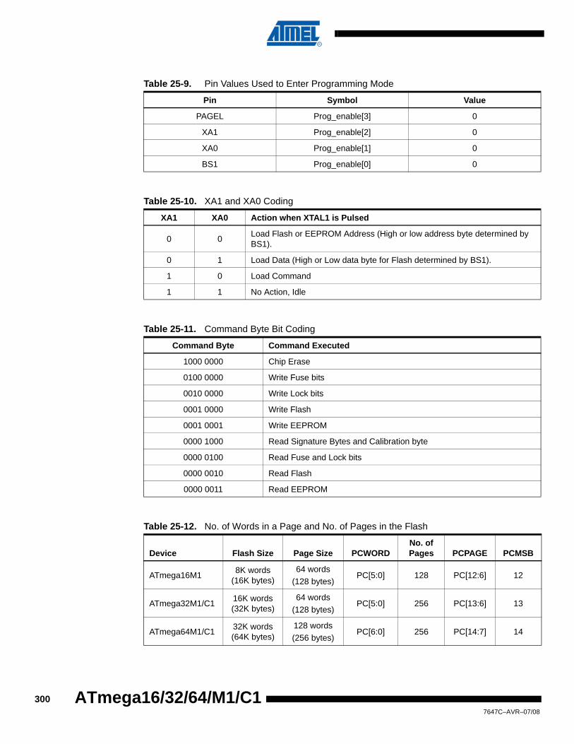
Table 25-9. Pin Values Used to Enter Programming Mode
Pin Symbol Value
PAGEL Prog_enable[3] 0
XA1 Prog_enable[2] 0
XA0 Prog_enable[1] 0
BS1 Prog_enable[0] 0
Table 25-10. XA1 and XA0 Coding
XA1 XA0 Action when XTAL1 is Pulsed
0 0 Load Flash or EEPROM Address (High or low address byte determined by BS1).
0 1 Load Data (High or Low data byte for Flash determined by BS1).
1 0 Load Command
1 1 No Action, Idle
Table 25-11. Command Byte Bit Coding
Command Byte Command Executed
1000 0000 Chip Erase
0100 0000 Write Fuse bits
0010 0000 Write Lock bits
0001 0000 Write Flash
0001 0001 Write EEPROM
0000 1000 Read Signature Bytes and Calibration byte
0000 0100 Read Fuse and Lock bits
0000 0010 Read Flash
0000 0011 Read EEPROM
Table 25-12. No. of Words in a Page and No. of Pages in the Flash
Device Flash Size Page Size PCWORDNo. of Pages PCPAGE PCMSB
ATmega16M1 8K words (16K bytes)
64 words(128 bytes)
PC[5:0] 128 PC[12:6] 12
ATmega32M1/C1 16K words (32K bytes)
64 words(128 bytes)
PC[5:0] 256 PC[13:6] 13
ATmega64M1/C1 32K words (64K bytes)
128 words(256 bytes)
PC[6:0] 256 PC[14:7] 14
3007647C–AVR–07/08
ATmega16/32/64/M1/C1

ATmega16/32/64/M1/C1
25.7 Serial Programming Pin Mapping
25.8 Parallel Programming
25.8.1 Enter Programming Mode
The following algorithm puts the device in Parallel (High-voltage) > Programming mode:1. Set Prog_enable pins listed in Table 25-9. to “0000”, RESET pin to “0” and Vcc to 0V.2. Apply 4.5 - 5.5V between VCC and GND. Ensure that Vcc reaches at least 1.8V within
the next 20µs.3. Wait 20 - 60µs, and apply 11.5 - 12.5V to RESET.4. Keep the Prog_enable pins unchanged for at least 10µs after the High-voltage has been
applied to ensure the Prog_enable Signature has been latched.5. Wait at least 300µs before giving any parallel programming commands.6. Exit Programming mode by power the device down or by bringing RESET pin to 0V.
If the rise time of the Vcc is unable to fulfill the requirements listed above, the following alterna-tive algorithm can be used.1. Set Prog_enable pins listed in Table 25-9. to “0000”, RESET pin to “0” and Vcc to 0V.2. Apply 4.5 - 5.5V between VCC and GND.3. Monitor Vcc, and as soon as Vcc reaches 0.9 - 1.1V, apply 11.5 - 12.5V to RESET.4. Keep the Prog_enable pins unchanged for at least 10µs after the High-voltage has been
applied to ensure the Prog_enable Signature has been latched.5. Wait until Vcc actually reaches 4.5 -5.5V before giving any parallel programming
commands.6. Exit Programming mode by power the device down or by bringing RESET pin to 0V.
25.8.2 Considerations for Efficient Programming
The loaded command and address are retained in the device during programming. For efficientprogramming, the following should be considered.• The command needs only be loaded once when writing or reading multiple memory
locations.
Table 25-13. No. of Words in a Page and No. of Pages in the EEPROM
DeviceEEPROM
SizePage Size PCWORD
No. of Pages PCPAGE EEAMSB
ATmega16M1 512 bytes 4 bytes EEA[1:0] 128 EEA[8:2] 9
ATmega32M1/C1 1024 bytes 4 bytes EEA[1:0] 256 EEA[9:2] 9
ATmega64M1/C1 2048 bytes 8 bytes EEA[2:0] 256 EEA[9:2] 9
Table 25-14. Pin Mapping Serial Programming
Symbol Pins I/O Description
MOSI_A PD3 I Serial Data in
MISO_A PD2 O Serial Data out
SCK_A PD4 I Serial Clock
3017647C–AVR–07/08

• Skip writing the data value 0xFF, that is the contents of the entire EEPROM (unless the EESAVE Fuse is programmed) and Flash after a Chip Erase.
• Address high byte needs only be loaded before programming or reading a new 256 word window in Flash or 256 byte EEPROM. This consideration also applies to Signature bytes reading.
25.8.3 Chip Erase
The Chip Erase will erase the Flash and EEPROM(1) memories plus Lock bits. The Lock bits arenot reset until the program memory has been completely erased. The Fuse bits are notchanged. A Chip Erase must be performed before the Flash and/or EEPROM arereprogrammed.Note: 1. The EEPRPOM memory is preserved during Chip Erase if the EESAVE Fuse is programmed.
Load Command “Chip Erase”1. Set XA1, XA0 to “10”. This enables command loading.2. Set BS1 to “0”.3. Set DATA to “1000 0000”. This is the command for Chip Erase.4. Give XTAL1 a positive pulse. This loads the command.5. Give WR a negative pulse. This starts the Chip Erase. RDY/BSY goes low.6. Wait until RDY/BSY goes high before loading a new command.
25.8.4 Programming the Flash
The Flash is organized in pages, see Table 25-12 on page 300. When programming the Flash,the program data is latched into a page buffer. This allows one page of program data to be pro-grammed simultaneously. The following procedure describes how to program the entire Flashmemory:
A. Load Command “Write Flash”1. Set XA1, XA0 to “10”. This enables command loading.2. Set BS1 to “0”.3. Set DATA to “0001 0000”. This is the command for Write Flash.4. Give XTAL1 a positive pulse. This loads the command.
B. Load Address Low byte1. Set XA1, XA0 to “00”. This enables address loading.2. Set BS1 to “0”. This selects low address.3. Set DATA = Address low byte (0x00 - 0xFF).4. Give XTAL1 a positive pulse. This loads the address low byte.
C. Load Data Low Byte1. Set XA1, XA0 to “01”. This enables data loading.2. Set DATA = Data low byte (0x00 - 0xFF).3. Give XTAL1 a positive pulse. This loads the data byte.
D. Load Data High Byte1. Set BS1 to “1”. This selects high data byte.2. Set XA1, XA0 to “01”. This enables data loading.3. Set DATA = Data high byte (0x00 - 0xFF).4. Give XTAL1 a positive pulse. This loads the data byte.
3027647C–AVR–07/08
ATmega16/32/64/M1/C1

ATmega16/32/64/M1/C1
E. Latch Data1. Set BS1 to “1”. This selects high data byte.2. Give PAGEL a positive pulse. This latches the data bytes. (See Figure 25-3 for signal
waveforms)
F. Repeat B through E until the entire buffer is filled or until all data within the page is loaded.
While the lower bits in the address are mapped to words within the page, the higher bits addressthe pages within the FLASH. This is illustrated in Figure 25-2 on page 303. Note that if less thaneight bits are required to address words in the page (pagesize < 256), the most significant bit(s)in the address low byte are used to address the page when performing a Page Write.
G. Load Address High byte1. Set XA1, XA0 to “00”. This enables address loading.2. Set BS1 to “1”. This selects high address.3. Set DATA = Address high byte (0x00 - 0xFF).4. Give XTAL1 a positive pulse. This loads the address high byte.
H. Program Page1. Give WR a negative pulse. This starts programming of the entire page of data. RDY/BSY
goes low.2. Wait until RDY/BSY goes high (See Figure 25-3 for signal waveforms).
I. Repeat B through H until the entire Flash is programmed or until all data has beenprogrammed.
J. End Page Programming1. 1. Set XA1, XA0 to “10”. This enables command loading.2. Set DATA to “0000 0000”. This is the command for No Operation.3. Give XTAL1 a positive pulse. This loads the command, and the internal write signals are
reset.
Figure 25-2. Addressing the Flash Which is Organized in Pages(1)
Note: 1. PCPAGE and PCWORD are listed in Table 25-12 on page 300.
PROGRAM MEMORY
WORD ADDRESSWITHIN A PAGE
PAGE ADDRESSWITHIN THE FLASH
INSTRUCTION WORD
PAGE PCWORD[PAGEMSB:0]:
00
01
02
PAGEEND
PAGE
PCWORDPCPAGE
PCMSB PAGEMSBPROGRAMCOUNTER
3037647C–AVR–07/08

Figure 25-3. Programming the Flash Waveforms(1)
Note: 1. “XX” is don’t care. The letters refer to the programming description above.
25.8.5 Programming the EEPROM
The EEPROM is organized in pages, see Table 25-13 on page 301. When programming theEEPROM, the program data is latched into a page buffer. This allows one page of data to beprogrammed simultaneously. The programming algorithm for the EEPROM data memory is asfollows (refer to “Programming the Flash” on page 302 for details on Command, Address andData loading):1. A: Load Command “0001 0001”.2. G: Load Address High Byte (0x00 - 0xFF).3. B: Load Address Low Byte (0x00 - 0xFF).4. C: Load Data (0x00 - 0xFF).5. E: Latch data (give PAGEL a positive pulse).
K: Repeat 3 through 5 until the entire buffer is filled.
L: Program EEPROM page1. Set BS1 to “0”.2. Give WR a negative pulse. This starts programming of the EEPROM page. RDY/BSY
goes low.3. Wait until to RDY/BSY goes high before programming the next page (See Figure 25-4 for
signal waveforms).
RDY/BSY
WR
OE
RESET +12V
PAGEL
BS2
0x10 ADDR. LOW ADDR. HIGHDATADATA LOW DATA HIGH ADDR. LOW DATA LOW DATA HIGH
XA1
XA0
BS1
XTAL1
XX XX XX
A B C D E B C D E G H
F
3047647C–AVR–07/08
ATmega16/32/64/M1/C1

ATmega16/32/64/M1/C1
Figure 25-4. Programming the EEPROM Waveforms
25.8.6 Reading the Flash
The algorithm for reading the Flash memory is as follows (refer to “Programming the Flash” onpage 302 for details on Command and Address loading):1. A: Load Command “0000 0010”.2. G: Load Address High Byte (0x00 - 0xFF).3. B: Load Address Low Byte (0x00 - 0xFF).4. Set OE to “0”, and BS1 to “0”. The Flash word low byte can now be read at DATA.5. Set BS1 to “1”. The Flash word high byte can now be read at DATA.6. Set OE to “1”.
25.8.7 Reading the EEPROM
The algorithm for reading the EEPROM memory is as follows (refer to “Programming the Flash”on page 302 for details on Command and Address loading):1. A: Load Command “0000 0011”.2. G: Load Address High Byte (0x00 - 0xFF).3. B: Load Address Low Byte (0x00 - 0xFF).4. Set OE to “0”, and BS1 to “0”. The EEPROM Data byte can now be read at DATA.5. Set OE to “1”.
25.8.8 Programming the Fuse Low Bits
The algorithm for programming the Fuse Low bits is as follows (refer to “Programming the Flash”on page 302 for details on Command and Data loading):1. A: Load Command “0100 0000”.2. C: Load Data Low Byte. Bit n = “0” programs and bit n = “1” erases the Fuse bit.3. Give WR a negative pulse and wait for RDY/BSY to go high.
25.8.9 Programming the Fuse High Bits
The algorithm for programming the Fuse High bits is as follows (refer to “Programming theFlash” on page 302 for details on Command and Data loading):
RDY/BSY
WR
OE
RESET +12V
PAGEL
BS2
0x11 ADDR. HIGHDATA
ADDR. LOW DATA ADDR. LOW DATA XX
XA1
XA0
BS1
XTAL1
XX
A G B C E B C E L
K
3057647C–AVR–07/08

1. A: Load Command “0100 0000”.2. C: Load Data Low Byte. Bit n = “0” programs and bit n = “1” erases the Fuse bit.3. Set BS1 to “1” and BS2 to “0”. This selects high data byte.4. Give WR a negative pulse and wait for RDY/BSY to go high.5. Set BS1 to “0”. This selects low data byte.
25.8.10 Programming the Extended Fuse Bits
The algorithm for programming the Extended Fuse bits is as follows (refer to “Programming theFlash” on page 302 for details on Command and Data loading):1. 1. A: Load Command “0100 0000”.2. 2. C: Load Data Low Byte. Bit n = “0” programs and bit n = “1” erases the Fuse bit.3. 3. Set BS1 to “0” and BS2 to “1”. This selects extended data byte.4. 4. Give WR a negative pulse and wait for RDY/BSY to go high.5. 5. Set BS2 to “0”. This selects low data byte.
Figure 25-5. Programming the FUSES Waveforms
25.8.11 Programming the Lock Bits
The algorithm for programming the Lock bits is as follows (refer to “Programming the Flash” onpage 302 for details on Command and Data loading):1. A: Load Command “0010 0000”.2. C: Load Data Low Byte. Bit n = “0” programs the Lock bit. If LB mode 3 is programmed
(LB1 and LB2 is programmed), it is not possible to program the Boot Lock bits by anyExternal Programming mode.
3. Give WR a negative pulse and wait for RDY/BSY to go high.
The Lock bits can only be cleared by executing Chip Erase.
25.8.12 Reading the Fuse and Lock Bits
The algorithm for reading the Fuse and Lock bits is as follows (refer to “Programming the Flash”on page 302 for details on Command loading):
RDY/BSY
WR
OE
RESET +12V
PAGEL
0x40DATA
DATA XX
XA1
XA0
BS1
XTAL1
A C
0x40 DATA XX
A C
Write Fuse Low byte Write Fuse high byte
0x40 DATA XX
A C
Write Extended Fuse byte
BS2
3067647C–AVR–07/08
ATmega16/32/64/M1/C1

ATmega16/32/64/M1/C1
1. A: Load Command “0000 0100”.2. Set OE to “0”, BS2 to “0” and BS1 to “0”. The status of the Fuse Low bits can now be
read at DATA (“0” means programmed).3. Set OE to “0”, BS2 to “1” and BS1 to “1”. The status of the Fuse High bits can now be
read at DATA (“0” means programmed).4. Set OE to “0”, BS2 to “1”, and BS1 to “0”. The status of the Extended Fuse bits can now
be read at DATA (“0” means programmed).5. Set OE to “0”, BS2 to “0” and BS1 to “1”. The status of the Lock bits can now be read at
DATA (“0” means programmed).6. Set OE to “1”.
Figure 25-6. Mapping Between BS1, BS2 and the Fuse and Lock Bits During Read
25.8.13 Reading the Signature Bytes
The algorithm for reading the Signature bytes is as follows (refer to “Programming the Flash” onpage 302 for details on Command and Address loading):1. A: Load Command “0000 1000”.2. B: Load Address Low Byte (0x00 - 0x02).3. Set OE to “0”, and BS1 to “0”. The selected Signature byte can now be read at DATA.4. Set OE to “1”.
25.8.14 Reading the Calibration Byte
The algorithm for reading the Calibration byte is as follows (refer to “Programming the Flash” onpage 302 for details on Command and Address loading):1. A: Load Command “0000 1000”.2. B: Load Address Low Byte, 0x00.3. Set OE to “0”, and BS1 to “1”. The Calibration byte can now be read at DATA.4. Set OE to “1”.
Lock Bits 0
1
BS2
Fuse High Byte
0
1
BS1
DATA
Fuse Low Byte 0
1
BS2
Extended Fuse Byte
3077647C–AVR–07/08

25.8.15 Parallel Programming Characteristics
Figure 25-7. Parallel Programming Timing, Including some General Timing Requirements
Figure 25-8. Parallel Programming Timing, Loading Sequence with Timing Requirements(1)
Note: 1. The timing requirements shown in Figure 25-7 (i.e., tDVXH, tXHXL, and tXLDX) also apply to load-ing operation.
Data & Contol(DATA, XA0/1, BS1, BS2)
XTAL1tXHXL
tWLWH
tDVXH tXLDX
tPLWL
tWLRH
WR
RDY/BSY
PAGEL tPHPL
tPLBXtBVPH
tXLWL
tWLBXtBVWL
WLRL
XTAL1
PAGEL
tPLXHXLXHt tXLPH
ADDR0 (Low Byte) DATA (Low Byte) DATA (High Byte) ADDR1 (Low Byte)DATA
BS1
XA0
XA1
LOAD ADDRESS(LOW BYTE)
LOAD DATA (LOW BYTE)
LOAD DATA(HIGH BYTE)
LOAD DATA LOAD ADDRESS(LOW BYTE)
3087647C–AVR–07/08
ATmega16/32/64/M1/C1

ATmega16/32/64/M1/C1
Figure 25-9. Parallel Programming Timing, Reading Sequence (within the Same Page) with Timing Requirements(1)
Note: 1. The timing requirements shown in Figure 25-7 (i.e., tDVXH, tXHXL, and tXLDX) also apply to read-ing operation.
Table 25-15. Parallel Programming Characteristics, VCC = 5V ± 10%
Symbol Parameter Min Typ Max Units
VPP Programming Enable Voltage 11.5 12.5 V
IPP Programming Enable Current 250 μA
tDVXH Data and Control Valid before XTAL1 High 67 ns
tXLXH XTAL1 Low to XTAL1 High 200 ns
tXHXL XTAL1 Pulse Width High 150 ns
tXLDX Data and Control Hold after XTAL1 Low 67 ns
tXLWL XTAL1 Low to WR Low 0 ns
tXLPH XTAL1 Low to PAGEL high 0 ns
tPLXH PAGEL low to XTAL1 high 150 ns
tBVPH BS1 Valid before PAGEL High 67 ns
tPHPL PAGEL Pulse Width High 150 ns
tPLBX BS1 Hold after PAGEL Low 67 ns
tWLBX BS2/1 Hold after WR Low 67 ns
tPLWL PAGEL Low to WR Low 67 ns
tBVWL BS1 Valid to WR Low 67 ns
tWLWH WR Pulse Width Low 150 ns
tWLRL WR Low to RDY/BSY Low 0 1 μs
tWLRH WR Low to RDY/BSY High(1) 3.7 4.5 ms
tWLRH_CE WR Low to RDY/BSY High for Chip Erase(2) 7.5 9 ms
tXLOL XTAL1 Low to OE Low 0 ns
XTAL1
OE
ADDR0 (Low Byte) DATA (Low Byte) DATA (High Byte) ADDR1 (Low Byte)DATA
BS1
XA0
XA1
LOAD ADDRESS(LOW BYTE)
READ DATA (LOW BYTE)
READ DATA(HIGH BYTE)
LOAD ADDRESS(LOW BYTE)
tBVDV
tOLDV
tXLOL
tOHDZ
3097647C–AVR–07/08

Notes: 1. tWLRH is valid for the Write Flash, Write EEPROM, Write Fuse bits and Write Lock bitscommands.
2. tWLRH_CE is valid for the Chip Erase command.
25.9 Serial DownloadingBoth the Flash and EEPROM memory arrays can be programmed using the serial SPI bus whileRESET is pulled to GND. The serial interface consists of pins SCK, MOSI (input) and MISO (out-put). After RESET is set low, the Programming Enable instruction needs to be executed firstbefore program/erase operations can be executed. NOTE, in Table 25-14 on page 301, the pinmapping for SPI programming is listed. Not all parts use the SPI pins dedicated for the internalSPI interface.
Figure 25-10. Serial Programming and Verify(1)
Notes: 1. If the device is clocked by the internal Oscillator, it is no need to connect a clock source to theXTAL1 pin.
2. VCC - 0.3V < AVCC < VCC + 0.3V, however, AVCC should always be within 1.8 - 5.5V
When programming the EEPROM, an auto-erase cycle is built into the self-timed programmingoperation (in the Serial mode ONLY) and there is no need to first execute the Chip Eraseinstruction. The Chip Erase operation turns the content of every memory location in both theProgram and EEPROM arrays into 0xFF.
Depending on CKSEL Fuses, a valid clock must be present. The minimum low and high periodsfor the serial clock (SCK) input are defined as follows:
Low:> 2 CPU clock cycles for fck < 12 MHz, 3 CPU clock cycles for fck >= 12 MHz
High:> 2 CPU clock cycles for fck < 12 MHz, 3 CPU clock cycles for fck >= 12 MHz
25.9.1 Serial Programming Algorithm
When writing serial data to the ATmega16/32/64/M1/C1, data is clocked on the rising edge ofSCK.
tBVDV BS1 Valid to DATA valid 0 250 ns
tOLDV OE Low to DATA Valid 250 ns
tOHDZ OE High to DATA Tri-stated 250 ns
Table 25-15. Parallel Programming Characteristics, VCC = 5V ± 10% (Continued)
Symbol Parameter Min Typ Max Units
VCC
GND
XTAL1
SCK_A
MISO_A
MOSI_A
RESET
+1.8 - 5.5V
AVCC
+1.8 - 5.5V(2)
3107647C–AVR–07/08
ATmega16/32/64/M1/C1

ATmega16/32/64/M1/C1
When reading data from the ATmega16/32/64/M1/C1, data is clocked on the falling edge ofSCK. See Figure 25-11 for timing details.
To program and verify the ATmega16/32/64/M1/C1 in the serial programming mode, the follow-ing sequence is recommended (See four byte instruction formats in Table 25-17):1. Power-up sequence:
Apply power between VCC and GND while RESET and SCK are set to “0”. In some sys-tems, the programmer can not guarantee that SCK is held low during power-up. In thiscase, RESET must be given a positive pulse of at least two CPU clock cycles durationafter SCK has been set to “0”.
2. Wait for at least 20 ms and enable serial programming by sending the ProgrammingEnable serial instruction to pin MOSI.
3. The serial programming instructions will not work if the communication is out of synchro-nization. When in sync. the second byte (0x53), will echo back when issuing the thirdbyte of the Programming Enable instruction. Whether the echo is correct or not, all fourbytes of the instruction must be transmitted. If the 0x53 did not echo back, give RESET apositive pulse and issue a new Programming Enable command.
4. The Flash is programmed one page at a time. The memory page is loaded one byte at atime by supplying the 6 LSB of the address and data together with the Load ProgramMemory Page instruction. To ensure correct loading of the page, the data low byte mustbe loaded before data high byte is applied for a given address. The Program MemoryPage is stored by loading the Write Program Memory Page instruction with the 8 MSB ofthe address. If polling is not used, the user must wait at least tWD_FLASH before issuing thenext page. (See Table 25-16.) Accessing the serial programming interface before theFlash write operation completes can result in incorrect programming.
5. The EEPROM array is programmed one byte at a time by supplying the address anddata together with the appropriate Write instruction. An EEPROM memory location is firstautomatically erased before new data is written. If polling is not used, the user must waitat least tWD_EEPROM before issuing the next byte. (See Table 25-16.) In a chip eraseddevice, no 0xFFs in the data file(s) need to be programmed.
6. Any memory location can be verified by using the Read instruction which returns the con-tent at the selected address at serial output MISO.
7. At the end of the programming session, RESET can be set high to commence normaloperation.
8. Power-off sequence (if needed):Set RESET to “1”.Turn VCC power off.
25.9.2 Data Polling Flash
When a page is being programmed into the Flash, reading an address location within the pagebeing programmed will give the value 0xFF. At the time the device is ready for a new page, theprogrammed value will read correctly. This is used to determine when the next page can be writ-ten. Note that the entire page is written simultaneously and any address within the page can beused for polling. Data polling of the Flash will not work for the value 0xFF, so when programmingthis value, the user will have to wait for at least tWD_FLASH before programming the next page. Asa chip-erased device contains 0xFF in all locations, programming of addresses that are meant tocontain 0xFF, can be skipped. See Table 25-16 for tWD_FLASH value.
25.9.3 Data Polling EEPROM
When a new byte has been written and is being programmed into EEPROM, reading theaddress location being programmed will give the value 0xFF. At the time the device is ready for
3117647C–AVR–07/08

a new byte, the programmed value will read correctly. This is used to determine when the nextbyte can be written. This will not work for the value 0xFF, but the user should have the followingin mind: As a chip-erased device contains 0xFF in all locations, programming of addresses thatare meant to contain 0xFF, can be skipped. This does not apply if the EEPROM is re-pro-grammed without chip erasing the device. In this case, data polling cannot be used for the value0xFF, and the user will have to wait at least tWD_EEPROM before programming the next byte. SeeTable 25-16 for tWD_EEPROM value.
Figure 25-11. Serial Programming Waveforms
Table 25-16. Minimum Wait Delay Before Writing the Next Flash or EEPROM Location
Symbol Minimum Wait Delay
tWD_FLASH 4.5 ms
tWD_EEPROM 3.6 ms
tWD_ERASE 9.0 ms
MSB
MSB
LSB
LSB
SERIAL CLOCK INPUT(SCK)
SERIAL DATA INPUT (MOSI)
(MISO)
SAMPLE
SERIAL DATA OUTPUT
Table 25-17. Serial Programming Instruction Set
Instruction
Instruction Format
OperationByte 1 Byte 2 Byte 3 Byte4
Programming Enable 1010 1100 0101 0011 xxxx xxxx xxxx xxxx Enable Serial Programming after RESET goes low.
Chip Erase 1010 1100 100x xxxx xxxx xxxx xxxx xxxx Chip Erase EEPROM and Flash.
Read Program Memory 0010 H000 000a aaaa bbbb bbbb oooo oooo Read H (high or low) data o from Program memory at word address a:b.
Load Program Memory Page
0100 H000 000x xxxx xxbb bbbb iiii iiii Write H (high or low) data i to Program Memory page at word address b. Data low byte must be loaded before Data high byte is applied within the same address.
Write Program Memory Page 0100 1100 000a aaaa bbxx xxxx xxxx xxxx Write Program Memory Page at address a:b.
Read EEPROM Memory 1010 0000 000x xxaa bbbb bbbb oooo oooo Read data o from EEPROM memory at address a:b.
Write EEPROM Memory 1100 0000 000x xxaa bbbb bbbb iiii iiii Write data i to EEPROM memory at address a:b.
3127647C–AVR–07/08
ATmega16/32/64/M1/C1

ATmega16/32/64/M1/C1
Note: a = address high bits, b = address low bits, H = 0 - Low byte, 1 - High Byte, o = data out, i = data in, x = don’t care
25.9.4 SPI Serial Programming Characteristics
For characteristics of the SPI module see “SPI Serial Programming Characteristics” on page313.
Load EEPROM Memory Page (page access)
1100 0001 0000 0000 0000 00bb iiii iiii Load data i to EEPROM memory page buffer. After data is loaded, program EEPROM page.
Write EEPROM Memory Page (page access)
1100 0010 00xx xxaa bbbb bb00 xxxx xxxx Write EEPROM page at address a:b.
Read Lock bits0101 1000 0000 0000 xxxx xxxx xxoo oooo Read Lock bits. “0” = programmed, “1”
= unprogrammed. See Table 25-1 on page 294 for details.
Write Lock bits1010 1100 111x xxxx xxxx xxxx 11ii iiii Write Lock bits. Set bits = “0” to
program Lock bits. See Table 25-1 on page 294 for details.
Read Signature Byte 0011 0000 000x xxxx xxxx xxbb oooo oooo Read Signature Byte o at address b.
Write Fuse bits1010 1100 1010 0000 xxxx xxxx iiii iiii Set bits = “0” to program, “1” to
unprogram. See Table XXX on page XXX for details.
Write Fuse High bits1010 1100 1010 1000 xxxx xxxx iiii iiii Set bits = “0” to program, “1” to
unprogram. See Table 25-6 on page 297 for details.
Write Extended Fuse Bits1010 1100 1010 0100 xxxx xxxx xxxx xxii Set bits = “0” to program, “1” to
unprogram. See Table 25-4 on page 295 for details.
Read Fuse bits0101 0000 0000 0000 xxxx xxxx oooo oooo Read Fuse bits. “0” = programmed, “1”
= unprogrammed. See Table XXX on page XXX for details.
Read Fuse High bits0101 1000 0000 1000 xxxx xxxx oooo oooo Read Fuse High bits. “0” = pro-
grammed, “1” = unprogrammed. See Table 25-6 on page 297 for details.
Read Extended Fuse Bits0101 0000 0000 1000 xxxx xxxx oooo oooo Read Extended Fuse bits. “0” = pro-
grammed, “1” = unprogrammed. See Table 25-4 on page 295 for details.
Read Calibration Byte 0011 1000 000x xxxx 0000 0000 oooo oooo Read Calibration Byte
Poll RDY/BSY1111 0000 0000 0000 xxxx xxxx xxxx xxxo If o = “1”, a programming operation is
still busy. Wait until this bit returns to “0” before applying another command.
Table 25-17. Serial Programming Instruction Set (Continued)
Instruction
Instruction Format
OperationByte 1 Byte 2 Byte 3 Byte4
3137647C–AVR–07/08

26. Electrical CharacteristicsAll DC/AC characteristics contained in this datasheet are based on simulations and character-ization of similar devices in the same process and design methods. These values arepreliminary representing design targets, and will be updated after characterization of actualautomotive silicon data.
26.1 Absolute Maximum Ratings*
Operating Temperature.................................. -40°C to +125°C *NOTICE: Stresses beyond those listed under “Absolute Maximum Ratings” may cause permanent dam-age to the device. This is a stress rating only and functional operation of the device at these or other conditions beyond those indicated in the operational sections of this specification is not implied. Exposure to absolute maximum rating conditions for extended periods may affect device reliability.
Storage Temperature ..................................... -65°C to +150°C
Voltage on any Pin except RESETwith respect to Ground ................................-0.5V to VCC+0.5V
Voltage on RESET with respect to Ground......-0.5V to +13.0V
Maximum Operating Voltage ............................................ 6.0V
DC Current per I/O Pin ............................................... 40.0 mA
DC Current VCC and GND Pins................................ 200.0 mA
3147647C–AVR–07/08
ATmega16/32/64/M1/C1
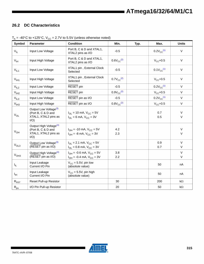
ATmega16/32/64/M1/C1
26.2 DC Characteristics
TA = -40°C to +125°C, VCC = 2.7V to 5.5V (unless otherwise noted)
Symbol Parameter Condition Min. Typ. Max. Units
VIL Input Low Voltage Port B, C & D and XTAL1, XTAL2 pins as I/O -0.5 0.2VCC
(1) V
VIH Input High Voltage Port B, C & D and XTAL1, XTAL2 pins as I/O 0.6VCC
(2) VCC+0.5 V
VIL1 Input Low Voltage XTAL1 pin , External Clock Selected -0.5 0.1VCC
(1) V
VIH1 Input High Voltage XTAL1 pin , External Clock Selected 0.7VCC
(2) VCC+0.5 V
VIL2 Input Low Voltage RESET pin -0.5 0.2VCC(1) V
VIH2 Input High Voltage RESET pin 0.9VCC(2) VCC+0.5 V
VIL3 Input Low Voltage RESET pin as I/O -0.5 0.2VCC(1) V
VIH3 Input High Voltage RESET pin as I/O 0.8VCC(2) VCC+0.5 V
VOL
Output Low Voltage(3)
(Port B, C & D and XTAL1, XTAL2 pins as I/O)
IOL = 10 mA, VCC = 5VIOL = 6 mA, VCC = 3V
0.70.5
VV
VOH
Output High Voltage(4)
(Port B, C & D and XTAL1, XTAL2 pins as I/O)
IOH = -10 mA, VCC = 5VIOH = -8 mA, VCC = 3V
4.22.3
VV
VOL3Output Low Voltage(3)
(RESET pin as I/O)IOL = 2.1 mA, VCC = 5VIOL = 0.8 mA, VCC = 3V
0.90.7
VV
VOH3Output High Voltage(4)
(RESET pin as I/O)IOH = -0.6 mA, VCC = 5VIOH = -0.4 mA, VCC = 3V
3.82.2
VV
IILInput LeakageCurrent I/O Pin
VCC = 5.5V, pin low(absolute value) 50 nA
IIHInput LeakageCurrent I/O Pin
VCC = 5.5V, pin high(absolute value) 50 nA
RRST Reset Pull-up Resistor 30 200 kΩ
Rpu I/O Pin Pull-up Resistor 20 50 kΩ
3157647C–AVR–07/08

Note: 1. “Max” means the highest value where the pin is guaranteed to be read as low2. “Min” means the lowest value where the pin is guaranteed to be read as high3. Although each I/O port can sink more than the test conditions (10 mA at VCC = 5V, 6 mA at VCC = 3V) under steady state
conditions (non-transient), the following must be observed:1] The sum of all IOL, for ports B0 - B1, C2 - C3, D4, E1 - E2 should not exceed 70 mA.2] The sum of all IOL, for ports B6 - B7, C0 - C1, D0 -D3, E0 should not exceed 70 mA.3] The sum of all IOL, for ports B2 - B5, C4 - C7, D5 - D7 should not exceed 70 mA.If IOL exceeds the test condition, VOL may exceed the related specification. Pins are not guaranteed to sink current greaterthan the listed test condition.
4. Although each I/O port can source more than the test conditions (10 mA at Vcc = 5V, 8 mA at Vcc = 3V) under steady stateconditions (non-transient), the following must be observed:1] The sum of all IOH, for ports B0 - B1, C2 - C3, D4, E1 - E2 should not exceed 100 mA.2] The sum of all IOH, for ports B6 - B7, C0 - C1, D0 -D3, E0 should not exceed 100 mA.3] The sum of all IOH, for ports B2 - B5, C4 - C7, D5 - D7 should not exceed 100 mA.If IOH exceeds the test condition, VOH may exceed the related specification. Pins are not guaranteed to source currentgreater than the listed test condition.
5. Minimum VCC for Power-down is 2.5V.6. The Analog Comparator Propogation Delay equals 1 comparator clock plus 30 nS. See “Analog Comparator” on page 259.
for comparator clock definition.
ICC
Power Supply Current
Active 8 MHz, VCC = 3V, RC osc, PRR = 0xFF 3.8 mA
Active 16 MHz, VCC = 5V, Ext Clock, PRR = 0xFF 14 mA
Idle 8 MHz, VCC = 3V, RC Osc 1.5 mA
Idle 16 MHz, VCC = 5V, Ext Clock 5.5 mA
Power-down mode(5)
WDT enabled, VCC = 3Vt0 < 90°C
5 µA
WDT enabled, VCC = 3Vt0 < 105°C
9 µA
WDT disabled, VCC = 3Vt0 < 90°C
2 µA
WDT disabled, VCC = 3Vt0 < 105°C
5 µA
VhysrAnalog Comparator Hysteresis Voltage
VCC = 5V, Vin = 3VRising EdgeFalling Edge
25-35
mVmV
IACLKAnalog Comparator Input Leakage Current
VCC = 5VVin = VCC/2 nA
tACIDAnalog Comparator Propagation Delay
VCC = 2.7VVCC = 5.0V
(6)(6) ns
ISRC Current Source Value VCC = 5V: Max Rload 30KΩVCC = 3V: Max Rload 15KΩ 97 100 103 µA
TA = -40°C to +125°C, VCC = 2.7V to 5.5V (unless otherwise noted) (Continued)
Symbol Parameter Condition Min. Typ. Max. Units
3167647C–AVR–07/08
ATmega16/32/64/M1/C1

ATmega16/32/64/M1/C1
26.3 Clock Characteristics
26.3.1 Calibrated Internal RC Oscillator Accuracy
26.4 External Clock Drive Characteristics
Figure 26-1. External Clock Drive Waveforms
26.5 Maximum Speed vs. VCC
Maximum frequency is depending on VCC. As shown in Figure 26-2 , the Maximum Frequencyequals 8MHz when VCC is between 2.7V and 4.5V and equals 16MHz when VCC is between 4.5Vand 5.5V.
Table 26-1. Calibration Accuracy of Internal RC Oscillator
Frequency VCC Temperature Calibration Accuracy
FactoryCalibration 8.0 MHz 3V 25°C ±1%
UserCalibration 7.3 - 8.1 MHz 2.7V - 5.5V -40°C - 125°C ±10%
Table 2. External Clock Drive
Symbol Parameter
VCC = 2.7 - 5.5V VCC = 4.5 - 5.5V
UnitsMin. Max. Min. Max.
1/tCLCL Oscillator Frequency 0 8 0 16 MHz
tCLCL Clock Period 125 62.5 ns
tCHCX High Time 50 25 ns
tCLCX Low Time 50 25 ns
tCLCH Rise Time 1.6 0.5 μs
tCHCL Fall Time 1.6 0.5 μs
ΔtCLCLChange in period from one clock cycle to the next 2 2 %
VIL1
VIH1
3177647C–AVR–07/08

Figure 26-2. Maximum Frequency vs. VCC, ATmega16/32/64/M1/C1
26.6 PLL Characteristics.
Note: While connected to external clock or external oscillator, PLL Input Frequency must be selected to provide outputs with frequency in accordance with driven parts of the circuit (CPU core, PSC...)
Safe Operating Area
16Mhz
8Mhz
2.7V 5.5V4.5V
Table 3. PLL Characteristics - VCC = 2.7V to 5.5V (unless otherwise noted)
Symbol Parameter Min. Typ. Max. Units
PLLIF Input Frequency 0.5 1 2 MHz
PLLF PLL Factor 64
PLLLT Lock-in Time 64 µS
3187647C–AVR–07/08
ATmega16/32/64/M1/C1

ATmega16/32/64/M1/C1
26.7 SPI Timing CharacteristicsSee Figure 26-3 and Figure 26-4 for details.
Note: In SPI Programming mode the minimum SCK high/low period is:- 2 tCLCL for fCK < 12 MHz- 3 tCLCL for fCK >12 MHz
Figure 26-3. SPI Interface Timing Requirements (Master Mode)
Table 4. SPI Timing Parameters
Description Mode Min. Typ. Max.
1 SCK period Master See Table 15-4
ns
2 SCK high/low Master 50% duty cycle
3 Rise/Fall time Master 3.6
4 Setup Master 10
5 Hold Master 10
6 Out to SCK Master 0.5 • tsck
7 SCK to out Master 10
8 SCK to out high Master 10
9 SS low to out Slave 15
10 SCK period Slave 4 • tck
11 SCK high/low (1) Slave 2 • tck
12 Rise/Fall time Slave 1600
13 Setup Slave 10
14 Hold Slave tck
15 SCK to out Slave 15
16 SCK to SS high Slave 20
17 SS high to tri-state Slave 10
18 SS low to SCK Slave 20
MOSI(Data Output)
SCK(CPOL = 1)
MISO(Data Input)
SCK(CPOL = 0)
SS
MSB LSB
LSBMSB
...
...
6 1
2 2
34 5
87
3197647C–AVR–07/08

Figure 26-4. SPI Interface Timing Requirements (Slave Mode)
MISO(Data Output)
SCK(CPOL = 1)
MOSI(Data Input)
SCK(CPOL = 0)
SS
MSB LSB
LSBMSB
...
...
10
11 11
1213 14
1715
9
X
16
3207647C–AVR–07/08
ATmega16/32/64/M1/C1
ATmega16/32/64/M1/C1
26.8 ADC Characteristics
Table 26-2. ADC Characteristics - TA = -40°C to +125°C, VCC = 2.7V to 5.5V (unless otherwise noted)
Symbol Parameter Condition Min Typ Max Units
ResolutionSingle Ended Conversion 10 Bits
Differential Conversion 8 Bits
Absolute accuracy
Single Ended ConversionVREF = 2.56VADC clock = 500 kHz
2.5 LSB
Single Ended ConversionVREF = 2.56VADC clock = 1MHz
6 LSB
Single Ended ConversionVREF = 2.56VADC clock = 2MHz
LSB
Differential ConversionVREF = 2.56VADC clock = 500 kHz
2 LSB
Differential ConversionVREF = 2.56VADC clock = 1MHz
3 LSB
Integral Non-linearity
Single Ended ConversionVCC = 4.5V, VREF = 2.56VADC clock = 1MHz
1.1 LSB
Single Ended ConversionVCC = 4.5V, VREF = 2.56VADC clock = 500 kHz
0.6 LSB
Differential ConversionVCC = 4.5V, VREF = 2.56VADC clock = 1MHz
1.5 LSB
Differential ConversionVCC = 4.5V, VREF = 2.56VADC clock = 500 kHz
1 LSB
Differential Non-linearity
Single Ended ConversionVCC = 4.5V, VREF = 4VADC clock = 1MHz
0.4 LSB
Single Ended ConversionVCC = 4.5V, VREF = 4VADC clock = 500 kHz
0.3 LSB
Differential ConversionVCC = 4.5V, VREF = 4VADC clock = 1MHz
0.5 LSB
Differential ConversionVCC = 4.5V, VREF = 4VADC clock = 500 kHz
0.4 LSB
3217647C–AVR–07/08

Zero Error (Offset)
Single Ended ConversionVCC = 4.5V, VREF = 4VADC clock = 1MHz
-4 0 LSB
Single Ended ConversionVCC = 4.5V, VREF = 4VADC clock = 500 kHz
-2 2.5 LSB
Differential ConversionVCC = 4.5V, VREF = 4VADC clock = 1MHz
-0.5 0.5 LSB
Differential ConversionVCC = 4.5V, VREF = 4VADC clock = 500 kHz
-0.5 0.5 LSB
Conversion Time Single Conversion 8 320 µs
Clock Frequency 50 2000 kHz
AVCC Analog Supply Voltage VCC - 0.3 VCC + 0.3 V
VREF Reference VoltageSingle Ended Conversion 2.0 AVCC V
Differential Conversion 2.0 AVCC - 0.2 V
VINInput voltage
Single Ended Conversion GND VREF
Differential Conversion -VREF/Gain +VREF/Gain
Input bandwidthSingle Ended Conversion 38.5 kHz
Differential Conversion 4 kHz
VINT Internal Voltage Reference 2.56 V
RREF Reference Input Resistance 30 kΩ
RAIN Analog Input Resistance 100 MΩ
IHSMIncreased Current Consumption
High Speed ModeSingle Ended Conversion
µA
Table 26-2. ADC Characteristics - TA = -40°C to +125°C, VCC = 2.7V to 5.5V (unless otherwise noted) (Continued)
Symbol Parameter Condition Min Typ Max Units
3227647C–AVR–07/08
ATmega16/32/64/M1/C1

ATmega16/32/64/M1/C1
26.9 Parallel Programming Characteristics
Figure 26-5. Parallel Programming Timing, Including some General Timing Requirements
Figure 26-6. Parallel Programming Timing, Loading Sequence with Timing Requirements(1)
Note: 1. The timing requirements shown in Figure 26-5 (i.e., tDVXH, tXHXL, and tXLDX) also apply to load-ing operation.
Data & Contol(DATA, XA0/1, BS1, BS2)
XTAL1tXHXL
tWLWH
tDVXH tXLDX
tPLWL
tWLRH
WR
RDY/BSY
PAGEL tPHPL
tPLBXtBVPH
tXLWL
tWLBXtBVWL
WLRL
XTAL1
PAGEL
tPLXHXLXHt tXLPH
ADDR0 (Low Byte) DATA (Low Byte) DATA (High Byte) ADDR1 (Low Byte)DATA
BS1
XA0
XA1
LOAD ADDRESS(LOW BYTE)
LOAD DATA (LOW BYTE)
LOAD DATA(HIGH BYTE)
LOAD DATA LOAD ADDRESS(LOW BYTE)
3237647C–AVR–07/08

Figure 26-7. Parallel Programming Timing, Reading Sequence (within the Same Page) with Timing Requirements(1)
Note: 1. ggThe timing requirements shown in Figure 26-5 (i.e., tDVXH, tXHXL, and tXLDX) also apply to reading operation.
XTAL1
OE
ADDR0 (Low Byte) DATA (Low Byte) DATA (High Byte) ADDR1 (Low Byte)DATA
BS1
XA0
XA1
LOAD ADDRESS(LOW BYTE)
READ DATA (LOW BYTE)
READ DATA(HIGH BYTE)
LOAD ADDRESS(LOW BYTE)
tBVDV
tOLDV
tXLOL
tOHDZ
Table 26-3. Parallel Programming Characteristics, VCC = 5V ± 10%
Symbol Parameter Min. Typ. Max. Units
VPP Programming Enable Voltage 11.5 12.5 V
IPP Programming Enable Current 250 μA
tDVXH Data and Control Valid before XTAL1 High 67 ns
tXLXH XTAL1 Low to XTAL1 High 200 ns
tXHXL XTAL1 Pulse Width High 150 ns
tXLDX Data and Control Hold after XTAL1 Low 67 ns
tXLWL XTAL1 Low to WR Low 0 ns
tXLPH XTAL1 Low to PAGEL high 0 ns
tPLXH PAGEL low to XTAL1 high 150 ns
tBVPH BS1 Valid before PAGEL High 67 ns
tPHPL PAGEL Pulse Width High 150 ns
tPLBX BS1 Hold after PAGEL Low 67 ns
tWLBX BS2/1 Hold after WR Low 67 ns
tPLWL PAGEL Low to WR Low 67 ns
tBVWL BS1 Valid to WR Low 67 ns
tWLWH WR Pulse Width Low 150 ns
tWLRL WR Low to RDY/BSY Low 0 1 μs
tWLRH WR Low to RDY/BSY High(1) 3.7 5 ms
tWLRH_CE WR Low to RDY/BSY High for Chip Erase(2) 7.5 10 ms
3247647C–AVR–07/08
ATmega16/32/64/M1/C1

ATmega16/32/64/M1/C1
Notes: 1. tWLRH is valid for the Write Flash, Write EEPROM, Write Fuse bits and Write Lock bitscommands.
2. tWLRH_CE is valid for the Chip Erase command.
27. ATmega16/32/64/M1/C1 Typical CharacteristicsAll DC characteristics contained in this datasheet are based on simulations and characterizationof similar devices in the same process and design methods. These values are preliminary repre-senting design targets, and will be updated after characterization of actual automotive silicondata.
The following charts show typical behavior. These figures are not tested during manufacturing.All current consumption measurements are performed with all I/O pins configured as inputs andwith internal pull-ups enabled. A sine wave generator with rail-to-rail output is used as clocksource.
All Active- and Idle current consumption measurements are done with all bits in the PRR registerset and thus, the corresponding I/O modules are turned off. Also the Analog Comparator is dis-abled during these measurements. Table 27-1 on page 330 and Table 27-2 on page 330 showthe additional current consumption compared to ICC Active and ICC Idle for every I/O module con-trolled by the Power Reduction Register. See “Power Reduction Register” on page 37 for details.
The power consumption in Power-down mode is independent of clock selection.
The current consumption is a function of several factors such as: operating voltage, operatingfrequency, loading of I/O pins, switching rate of I/O pins, code executed and ambient tempera-ture. The dominating factors are operating voltage and frequency.
The current drawn from capacitive loaded pins may be estimated (for one pin) as CL*VCC*f whereCL = load capacitance, VCC = operating voltage and f = average switching frequency of I/O pin.
The parts are characterized at frequencies higher than test limits. Parts are not guaranteed tofunction properly at frequencies higher than the ordering code indicates.
The difference between current consumption in Power-down mode with Watchdog Timerenabled and Power-down mode with Watchdog Timer disabled represents the differential cur-rent drawn by the Watchdog Timer.
tXLOL XTAL1 Low to OE Low 0 ns
tBVDV BS1 Valid to DATA valid 0 250 ns
tOLDV OE Low to DATA Valid 250 ns
tOHDZ OE High to DATA Tri-stated 250 ns
Table 26-3. Parallel Programming Characteristics, VCC = 5V ± 10% (Continued)
Symbol Parameter Min. Typ. Max. Units
3257647C–AVR–07/08

27.1 Active Supply Current
Figure 27-1. Active Supply Current vs. Frequency (0.1 - 1.0 MHz)
Figure 27-2. Active Supply Current vs. Frequency (1 - 24 MHz)
ACTIVE SUPPLY CURRENT vs. LOW FREQUENCY
5.5 V5.0 V4.5 V4.0 V
3.3 V3.0 V2.7 V
0
0.2
0.4
0.6
0.8
1
1.2
1.4
1.6
0 0.2 0.4 0.6 0.8 1Frequency (MHz)
I CC (m
A)
ACTIVE SUPPLY CURRENT vs. FREQUENCY
5.5 V
5.0 V
4.5 V
4.0 V
3.3 V3.0 V
2.7 V
0
5
10
15
20
25
30
0 5 10 15 20 25
Frequency (MHz)
I CC (m
A)
3267647C–AVR–07/08
ATmega16/32/64/M1/C1

ATmega16/32/64/M1/C1
Figure 27-3. Active Supply Current vs. VCC (Internal RC Oscillator, 8 MHz)
Figure 27-4. Active Supply Current vs. VCC (Internal PLL Oscillator, 16 MHz)
ACTIVE SUPPLY CURRENT vs. VCCINTERNAL RC OSCILLATOR, 8 MHz
105 °C85 °C25 °C-40 °C
0
1
2
3
4
5
6
7
8
9
2 2,5 3 3,5 4 4,5 5 5,5
VCC (V)
I CC (m
A)
ACTIVE SUPPLY CURRENT vs. VCCINTERNAL PLL OSCILLATOR, 16 MHz
105 °C85 °C25 °C-40 °C
0
2
4
6
8
10
12
14
16
18
20
2 2,5 3 3,5 4 4,5 5 5,5
VCC (V)
I CC (m
A)
3277647C–AVR–07/08

27.2 Idle Supply Current
Figure 27-5. Idle Supply Current vs. Frequency (0.1 - 1.0 MHz)
Figure 27-6. Idle Supply Current vs. Frequency (1 - 24 MHz)
IDLE SUPPLY CURRENT vs. LOW FREQUENCY
5.5 V
5.0 V
4.5 V
4.0 V
3.3 V3.0 V2.7 V
0
0,05
0,1
0,15
0,2
0,25
0,3
0,35
0,4
0,45
0 0,1 0,2 0,3 0,4 0,5 0,6 0,7 0,8 0,9 1
Frequency (MHz)
I CC (m
A)
IDLE SUPPLY CURRENT vs. FREQUENCY
5.5 V
5.0 V
4.5 V
4.0 V
3.3 V3.0 V
2.7 V
0
2
4
6
8
10
12
-1 1 3 5 7 9 11 13 15 17 19 21 23 25
Frequency (MHz)
I CC (m
A)
3287647C–AVR–07/08
ATmega16/32/64/M1/C1

ATmega16/32/64/M1/C1
Figure 27-7. IIdle Supply Current vs. VCC (Internal RC Oscillator, 8 MHz)
Figure 27-8. Idle Supply Current vs. VCC (Internal PLL Oscillator, 16 MHz)
27.2.1 Using the Power Reduction Register
The tables and formulas below can be used to calculate the additional current consumption forthe different I/O modules in Active and Idle mode. The enabling or disabling of the I/O modules
IDLE SUPPLY CURRENT vs. VCCINTERNAL RC OSCILLATOR, 8 MHz
105 °C85 °C25 °C-40 °C
0
0,5
1
1,5
2
2,5
3
3,5
4
2 2,5 3 3,5 4 4,5 5 5,5
VCC (V)
I CC (m
A)
IDLE SUPPLY CURRENT vs. VCCINTERNAL PLL OSCILLATOR, 16 MHz
105 °C85 °C25 °C-40 °C
0
1
2
3
4
5
6
7
8
9
2 2,5 3 3,5 4 4,5 5 5,5
VCC (V)
I CC (m
A)
3297647C–AVR–07/08

are controlled by the Power Reduction Register. See “Power Reduction Register” on page 42 fordetails.
It is possible to calculate the typical current consumption based on the numbers from Table 27-2for other VCC and frequency settings than listed in Table 27-1.
Table 27-1. Additional Current Consumption for the different I/O modules (absolute values)
PRR bit Typical numbers
VCC = 3V, F = 8MHz VCC = 5V, F = 16MHz
PRCAN
PRPSC
PRTIM1
PRTIM0
PRSPI
PRLIN
PRADC
Table 27-2. Additional Current Consumption (percentage) in Active and Idle mode
PRR bit
Additional Current consumption compared to Active with external clock (see Figure 27-1 and Figure 27-2)
Additional Current consumption compared to Idle with external clock (see Figure 27-5 and Figure 27-6)
PRCAN
PRPSC
PRTIM1
PRTIM0
PRSPI
PRLIN
PRADC
3307647C–AVR–07/08
ATmega16/32/64/M1/C1

ATmega16/32/64/M1/C1
27.3 Power-Down Supply Current
Figure 27-9. Power-Down Supply Current vs. VCC (Watchdog Timer Disabled)
Figure 27-10. Power-Down Supply Current vs. VCC (Watchdog Timer Enabled)
POWER-DOWN SUPPLY CURRENT vs. VCCWATCHDOG TIMER DISABLED
105 °C
85 °C
25 °C-40 °C
0
1
2
3
4
5
6
7
2 2,5 3 3,5 4 4,5 5 5,5
VCC (V)
I CC (u
A)
POWER-DOWN SUPPLY CURRENT vs. VCCWATCHDOG TIMER ENABLED
105 °C
85 °C
25 °C-40 °C
0
2
4
6
8
10
12
14
2 2,5 3 3,5 4 4,5 5 5,5
VCC (V)
I CC (u
A)
3317647C–AVR–07/08

27.4 Standby Supply Current
Figure 27-11. Standby Supply Current vs. VCC (Crystal Oscillator)
27.5 Pin Pull-up
Figure 27-12. I/O Pin Pull-Up Resistor Current vs. Input Voltage (VCC = 5V)
STANDBY SUPPLY CURRENT vs. VCC
Full Swing Crystal Oscillator
6 MHz Xtal (ckopt)
4 MHz Xtal (ckopt)
2 MHz Xtal(ckopt)
16 MHz Xtal
12 MHz Xtal
0
50
100
150
200
250
300
350
400
450
500
1.5 2 2.5 3 3.5 4 4.5 5 5.5
VCC (V)
I CC (
uA
) TEMPLATE
TO BE CHARACTERIZED
I/O PIN (including PE1 & PE2) PULL-UP RESISTOR CURRENT vs. INPUT VOLTAGEVcc = 5.0 V
105 °C85 °C25 °C
-40 °C
-20
0
20
40
60
80
100
120
140
160
0 1 2 3 4 5 6
VOP (V)
I OP
(uA
)
3327647C–AVR–07/08
ATmega16/32/64/M1/C1

ATmega16/32/64/M1/C1
Figure 27-13. I/O Pin Pull-Up Resistor Current vs. Input Voltage (VCC = 2.7V)
Figure 27-14. Reset Pull-Up Resistor Current vs. Reset Pin Voltage (VCC = 5V)
I/O PIN (including PE1 & PE2) PULL-UP RESISTOR CURRENT vs. INPUT VOLTAGEVcc = 2.7 V
105 °C85 °C25 °C
-40 °C
-10
0
10
20
30
40
50
60
70
80
90
0 0,5 1 1,5 2 2,5 3
VOP (V)
I OP
(uA)
PE0 and RESET PULL-UP RESISTOR CURRENT vs. INPUT VOLTAGEVcc = 5.0 V
105 °C85 °C
25 °C-40 °C
0
20
40
60
80
100
120
0 1 2 3 4 5 6
VOP (V)
I OP
(uA
)
3337647C–AVR–07/08

Figure 27-15. Reset Pull-Up Resistor Current vs. Reset Pin Voltage (VCC = 2.7V)
27.6 Pin Driver Strength
Figure 27-16. I/O Pin Source Current vs. Output Voltage (VCC = 5V)
PE0 and RESET PULL-UP RESISTOR CURRENT vs. INPUT VOLTAGEVcc = 2.7 V
105 °C85 °C
25 °C-40 °C
0
10
20
30
40
50
60
70
0 0,5 1 1,5 2 2,5 3
VOP (V)
I OP
(uA
)
I/O PIN (including PE1 & PE2) SOURCE CURRENT vs. OUTPUT VOLTAGEVcc = 5.0 V
105 °C
85 °C 25 °C -40 °C
0
5
10
15
20
25
4 4,2 4,4 4,6 4,8 5 5,2
VOH (V)
I OH
(mA
)
3347647C–AVR–07/08
ATmega16/32/64/M1/C1

ATmega16/32/64/M1/C1
Figure 27-17. I/O Pin Source Current vs. Output Voltage (VCC = 2.7V)
Figure 27-18. I/O Pin Sink Current vs. Output Voltage (VCC = 5V)
I/O PIN (including PE1 & PE2) SOURCE CURRENT vs. OUTPUT VOLTAGEVcc = 2.7 V
105 °C 85 °C 25 °C -40 °C
0
5
10
15
20
25
0 0,5 1 1,5 2 2,5 3
VOH (V)
I OH
(mA)
I/O PIN (including PE1 & PE2) SINK CURRENT vs. OUTPUT VOLTAGEVcc = 5.0 V
105 °C85 °C25 °C-40 °C
-5
0
5
10
15
20
25
0 0,2 0,4 0,6 0,8 1
VOL (V)
I OL (
mA
)
3357647C–AVR–07/08

Figure 27-19. I/O Pin Sink Current vs. Output Voltage (VCC = 2.7V)
27.7 Pin Thresholds and Hysteresis
Figure 27-20. I/O Pin Input Threshold Voltage vs. VCC (VIH, I/O Pin Read As '1')
I/O PIN (including PE1 & PE2) SINK CURRENT vs. OUTPUT VOLTAGEVcc = 2.7 V
105 °C85 °C25 °C-40 °C
-5
0
5
10
15
20
25
0 0,5 1 1,5 2 2,5 3
VOL (V)
I OL (
mA)
I/O PIN (including PE1 & PE2) INPUT THRESHOLD VOLTAGE vs. VCCVIH, IO PIN READ AS '1'
105 °C85 °C25 °C-40 °C
0
0,5
1
1,5
2
2,5
2 2,5 3 3,5 4 4,5 5 5,5
VCC (V)
Thre
shol
d (V
)
3367647C–AVR–07/08
ATmega16/32/64/M1/C1

ATmega16/32/64/M1/C1
Figure 27-21. I/O Pin Input Threshold Voltage vs. VCC (VIL, I/O Pin Read As '0')
Figure 27-22. I/O Pin Input HysteresisVoltage vs. VCC
I/O PIN (including PE1 & PE2) INPUT THRESHOLD VOLTAGE vs. VCCVIL, IO PIN READ AS '0'
105 °C85 °C25 °C-40 °C
0
0,5
1
1,5
2
2,5
2 2,5 3 3,5 4 4,5 5 5,5
VCC (V)
Thre
shol
d (V
)
I/O PIN INPUT HYSTERESIS vs. VCC
0
0.1
0.2
0.3
0.4
0.5
0.6
1.5 2 2.5 3 3.5 4 4.5 5 5.5
VCC (V)
Inpu
t Hys
tere
sis
(V)
85�C
25�C
-40�C
3377647C–AVR–07/08

Figure 27-23. Reset Input Threshold Voltage vs. VCC (VIH, Reset Pin Read As '1')
Figure 27-24. Reset Input Threshold Voltage vs. VCC (VIL, Reset Pin Read As '0')
RESET INPUT THRESHOLD VOLTAGE vs. VCCVIH, RESET PIN READ AS '1'
105 °C85 °C25 °C
-40 °C
0
0,5
1
1,5
2
2,5
2 2,5 3 3,5 4 4,5 5 5,5
VCC (V)
Thre
shol
d (V
)
RESET INPUT THRESHOLD VOLTAGE vs. VCCVIL, RESET PIN READ AS '0'
105 °C85 °C25 °C-40 °C
0
0,5
1
1,5
2
2,5
2 2,5 3 3,5 4 4,5 5 5,5
VCC (V)
Thre
shol
d (V
)
3387647C–AVR–07/08
ATmega16/32/64/M1/C1

ATmega16/32/64/M1/C1
Figure 27-25. Reset Input Pin Hysteresis vs. VCC
Figure 27-26. XTAL1 Input Threshold Voltage vs. VCC (XTAL1 Pin Read As '1')
RESET PIN INPUT HYSTERESIS vs. VCC
105 °C85 °C
25 °C
-40 °C
0
0,1
0,2
0,3
0,4
0,5
0,6
2 2,5 3 3,5 4 4,5 5 5,5
VCC (V)
Inpu
t Hys
tere
sis
(V)
XTAL1 INPUT THRESHOLD VOLTAGE vs. VCCXTAL1 PIN READ AS "1"
105 °C85 °C25 °C-40 °C
0
0,5
1
1,5
2
2,5
3
3,5
4
2 2,5 3 3,5 4 4,5 5 5,5
VCC (V)
Thre
shol
d (V
)
3397647C–AVR–07/08

Figure 27-27. XTAL1 Input Threshold Voltage vs. VCC (XTAL1 Pin Read As '0')
Figure 27-28. PE0 Input Threshold Voltage vs. VCC (PE0 Pin Read As '1')
XTAL1 INPUT THRESHOLD VOLTAGE vs. VCCXTAL1 PIN READ AS "0"
105 °C85 °C25 °C-40 °C
0
0,5
1
1,5
2
2,5
3
3,5
4
2 2,5 3 3,5 4 4,5 5 5,5
VCC (V)
Thre
shol
d (V
)
PE0 INPUT THRESHOLD VOLTAGE vs. VCCVIH, PE0 PIN READ AS '1'
105 °C85 °C25 °C-40 °C
0
0,5
1
1,5
2
2,5
3
3,5
4
2 2,5 3 3,5 4 4,5 5 5,5
VCC (V)
Thre
shol
d (V
)
3407647C–AVR–07/08
ATmega16/32/64/M1/C1

ATmega16/32/64/M1/C1
Figure 27-29. PE0 Input Threshold Voltage vs. VCC (PE0 Pin Read As '0')
27.8 BOD Thresholds and Analog Comparator Hysterisis
Figure 27-30. BOD Thresholds vs. Temperature (BODLEVEL Is 4.3V)
PE0 INPUT THRESHOLD VOLTAGE vs. VCCVIL, PE0 PIN READ AS '0'
105 °C85 °C25 °C-40 °C
0
0,5
1
1,5
2
2,5
2 2,5 3 3,5 4 4,5 5 5,5
VCC (V)
Thre
shol
d (V
)
BOD THRESHOLDS vs. TEMPERATUREBODLV IS 4.3 V
Rising Vcc
Falling Vcc
4,28
4,3
4,32
4,34
4,36
4,38
4,4
4,42
-50 -40 -30 -20 -10 0 10 20 30 40 50 60 70 80 90 100 110 120
Temperature (C)
Thre
shol
d (V
)
3417647C–AVR–07/08

Figure 27-31. BOD Thresholds vs. Temperature (BODLEVEL Is 2.7V)
Figure 27-32. TypicalAnalog Comparator Hysterisis Average Thresholds vs. Common Mode Voltage
BOD THRESHOLDS vs. TEMPERATUREBODLV IS 2.7 V
Rising Vcc
Falling Vcc
2,68
2,7
2,72
2,74
2,76
2,78
2,8
2,82
-50 -40 -30 -20 -10 0 10 20 30 40 50 60 70 80 90 100 110 120
Temperature (C)
Thre
shol
d (V
)
-60.00E-3
-50.00E-3
-40.00E-3
-30.00E-3
-20.00E-3
-10.00E-3
000.00E+0
10.00E-3
20.00E-3
30.00E-3
40.00E-3
0.5 1 1.35 1.5 2 2.5 2.6 2.75 3 3.5 4 4.5 5 5.4
Common voltage (v)
thre
shol
d va
lue
(V)
3427647C–AVR–07/08
ATmega16/32/64/M1/C1

ATmega16/32/64/M1/C1
27.9 Analog Reference
Figure 27-33. AREF Voltage vs. VCC
Figure 27-34. AREF Voltage vs. Temperature
AREF VOLTAGE vs. VCC
105 °C85 °C25 °C
-40 °C
2,3
2,35
2,4
2,45
2,5
2,55
2,6
2 2,5 3 3,5 4 4,5 5 5,5
Vcc (V)
Are
f (V
)
AREF VOLTAGE vs. TEMPERATURE
5.554.53
2.52
2.53
2.54
2.55
2.56
2.57
2.58
2.59
-60 -40 -20 0 20 40 60 80 100 120
Temperature
Aref
(V)
3437647C–AVR–07/08
27.10 Internal Oscillator Speed
Figure 27-35. Watchdog Oscillator Frequency vs. VCC
Figure 27-36. Calibrated 8 MHz RC Oscillator Frequency vs. Temperature
WATCHDOG OSCILLATOR FREQUENCY vs. OPERATING VOLTAGE
105 °C
85 °C
25 °C
-40 °C
96
98
100
102
104
106
108
110
2 2,5 3 3,5 4 4,5 5 5,5
VCC (V)
F RC (k
Hz)
CALIBRATED 8 MHz RC OSCILLATOR FREQUENCY vs. TEMPERATURE
5.0 V
2.7 V
1.8 V
7.4
7.5
7.6
7.7
7.8
7.9
8
8.1
8.2
8.3
8.4
-50 -40 -30 -20 -10 0 10 20 30 40 50 60 70 80 90 100
Temperature (C)
FR
C (
MH
z) TEMPLATE
TO BE CHARACTERIZED
3447647C–AVR–07/08
ATmega16/32/64/M1/C1

ATmega16/32/64/M1/C1
Figure 27-37. Calibrated 8 MHz RC Oscillator Frequency vs. VCC
Figure 27-38. Calibrated 8 MHz RC Oscillator Frequency vs. Osccal Value
CALIBRATED 8MHz RC OSCILLATOR FREQUENCY vs. V
85 ˚C
25 ˚C
-40 ˚C
7.4
7.6
7.8
8
8.2
8.4
8.6
1.5 2 2.5 3 3.5 4 4.5 5 5.5
VCC (V)
FR
C (
MH
z)
CC
TEMPLATE
TO BE CHARACTERIZED
CALIBRATED 8.0 MHz RC OSCILLATOR FREQUENCY vs. OSCCAL VALUE
105 °C85 °C25 °C-40 °C
0
2
4
6
8
10
12
14
16
-1 15 31 47 63 79 95 111 127 143 159 175 191 207 223 239 255
OSCCAL (X1)
F RC (M
Hz)
3457647C–AVR–07/08
27.11 Current Consumption of Peripheral Units
Figure 27-39. Brownout Detector Current vs. VCC
Figure 27-40. ADC Current vs. VCC (ADC at 50 kHz)
BROWNOUT DETECTOR CURRENT vs. VCC
105 °C85 °C25 °C-40 °C
0
5
10
15
20
25
30
35
40
45
2 2,5 3 3,5 4 4,5 5 5,5
VCC (V)
I CC (u
A)
AREF vs. VCC
ADC AT 50 KHz
85 °C
25 °C
-40 °C
150
200
250
300
350
400
450
500
1.5 2 2.5 3 3.5 4 4.5 5 5.5
VCC (V)
I CC (
uA)
TEMPLATE
TO BE CHARACTERIZED
3467647C–AVR–07/08
ATmega16/32/64/M1/C1

ATmega16/32/64/M1/C1
Figure 27-41. Aref Current vs. VCC (ADC at 1 MHz)
Figure 27-42. Analog Comparator Current vs. VCC
AREF vs. VCC
ADC AT 1 MHz
85 ˚C25 ˚C
-40 ˚C
0
20
40
60
80
100
120
140
160
180
1.5 2 2.5 3 3.5 4 4.5 5 5.5
VCC (V)
I CC (
uA)
ANALOG COMPARATOR CURRENT vs. VCC
105 °C85 °C25 °C
-40 °C
0
10
20
30
40
50
60
70
80
2 2,5 3 3,5 4 4,5 5 5,5
VCC (V)
I CC (u
A)
3477647C–AVR–07/08

Figure 27-43. Programming Current vs. VCC
27.12 Current Consumption in Reset and Reset Pulse width
Figure 27-44. Reset Supply Current vs. VCC (0.1 - 1.0 MHz, Excluding Current through the Reset Pull-up)
PROGRAMMING CURRENT vs. V
85 ˚C
25 ˚C
-40 ˚C
0
2
4
6
8
10
12
14
1.5 2 2.5 3 3.5 4 4.5 5 5.5
VCC (V)
I CC (
mA
)
cc
RESET SUPPLY CURRENT vs. VCCEXCLUDING CURRENT THROUGH THE RESET PULLUP
5.5 V
5.0 V
4.5 V
4.0 V
3.3 V3.0 V2.7 V
0
0,02
0,04
0,06
0,08
0,1
0,12
0,14
0,16
0,18
0 0,1 0,2 0,3 0,4 0,5 0,6 0,7 0,8 0,9 1
Frequency (MHz)
I CC (m
A)
3487647C–AVR–07/08
ATmega16/32/64/M1/C1

ATmega16/32/64/M1/C1
Figure 27-45. Reset Supply Current vs. VCC (1 - 24 MHz, Excluding Current through the Reset Pull-up)
Figure 27-46. Reset Supply Current vs. VCC (Clock Stopped, Excluding Current through the Reset Pull-up)
RESET SUPPLY CURRENT vs. VCCEXCLUDING CURRENT THROUGH THE RESET PULLUP
5.5 V
5.0 V
4.5 V
4.0 V
3.3 V3.0 V
2.7 V
0
0,5
1
1,5
2
2,5
3
3,5
4
0 5 10 15 20 25
Frequency (MHz)
I CC (m
A)
RESET CURRENT vs. VCC (CLOCK STOPPED)EXCLUDING CURRENT THROUGH THE RESET PULLUP
105 °C
85 °C25 °C
-40 °C
-0,01
0
0,01
0,02
0,03
0,04
0,05
2 2,5 3 3,5 4 4,5 5 5,5
VCC (V)
I CC (m
A)
3497647C–AVR–07/08

Figure 27-47. Reset Pulse Width vs. VCC
RESET PULSE WIDTH vs. VCCExt Clock 1 MHz
105 °C85 °C25 °C-40 °C
0
200
400
600
800
1000
1200
1400
1600
0 1 2 3 4 5 6
VCC (V)
Pul
sew
idth
(ns)
3507647C–AVR–07/08
ATmega16/32/64/M1/C1

ATmega16/32/64/M1/C1
28. Register SummaryAddress Name Bit 7 Bit 6 Bit 5 Bit 4 Bit 3 Bit 2 Bit 1 Bit 0 Page
(0xFF) Reserved – – – – – – – –(0xFE) Reserved – – – – – – – –(0xFD) Reserved – – – – – – – –(0xFC) Reserved – – – – – – – –(0xFB) Reserved – – – – – – – –(0xFA) CANMSG MSG 7 MSG 6 MSG 5 MSG 4 MSG 3 MSG 2 MSG 1 MSG 0 page 199(0xF9) CANSTMPH TIMSTM15 TIMSTM14 TIMSTM13 TIMSTM12 TIMSTM11 TIMSTM10 TIMSTM9 TIMSTM8 page 199(0xF8) CANSTMPL TIMSTM7 TIMSTM6 TIMSTM5 TIMSTM4 TIMSTM3 TIMSTM2 TIMSTM1 TIMSTM0 page 199(0xF7) CANIDM1 IDMSK28 IDMSK27 IDMSK26 IDMSK25 IDMSK24 IDMSK23 IDMSK22 IDMSK21 page 198(0xF6) CANIDM2 IDMSK20 IDMSK19 IDMSK18 IDMSK17 IDMSK16 IDMSK15 IDMSK14 IDMSK13 page 198(0xF5) CANIDM3 IDMSK12 IDMSK11 IDMSK10 IDMSK9 IDMSK8 IDMSK7 IDMSK6 IDMSK5 page 198(0xF4) CANIDM4 IDMSK4 IDMSK3 IDMSK2 IDMSK1 IDMSK0 RTRMSK – IDEMSK page 198(0xF3) CANIDT1 IDT28 IDT27 IDT26 IDT25 IDT24 IDT23 IDT22 IDT21 page 196(0xF2) CANIDT2 IDT20 IDT19 IDT18 IDT17 IDT16 IDT15 IDT14 IDT13 page 196(0xF1) CANIDT3 IDT12 IDT11 IDT10 IDT9 IDT8 IDT7 IDT6 IDT5 page 196(0xF0) CANIDT4 IDT4 IDT3 IDT2 IDT1 IDT0 RTRTAG RB1TAG RB0TAG page 196(0xEF) CANCDMOB CONMOB1 CONMOB0 RPLV IDE DLC3 DLC2 DLC1 DLC0 page 195(0xEE) CANSTMOB DLCW TXOK RXOK BERR SERR CERR FERR AERR page 194(0xED) CANPAGE MOBNB3 MOBNB2 MOBNB1 MOBNB0 AINC INDX2 INDX1 INDX0 page 194(0xEC) CANHPMOB HPMOB3 HPMOB2 HPMOB1 HPMOB0 CGP3 CGP2 CGP1 CGP0 page 193(0xEB) CANREC REC7 REC6 REC5 REC4 REC3 REC2 REC1 REC0 page 193(0xEA) CANTEC TEC7 TEC6 TEC5 TEC4 TEC3 TEC2 TEC1 TEC0 page 193(0xE9) CANTTCH TIMTTC15 TIMTTC14 TIMTTC13 TIMTTC12 TIMTTC11 TIMTTC10 TIMTTC9 TIMTTC8 page 193(0xE8) CANTTCL TIMTTC7 TIMTTC6 TIMTTC5 TIMTTC4 TIMTTC3 TIMTTC2 TIMTTC1 TIMTTC0 page 193(0xE7) CANTIMH CANTIM15 CANTIM14 CANTIM13 CANTIM12 CANTIM11 CANTIM10 CANTIM9 CANTIM8 page 193(0xE6) CANTIML CANTIM7 CANTIM6 CANTIM5 CANTIM4 CANTIM3 CANTIM2 CANTIM1 CANTIM0 page 193(0xE5) CANTCON TPRSC7 TPRSC6 TPRSC5 TPRSC4 TPRSC3 TPRSC2 TRPSC1 TPRSC0 page 192(0xE4) CANBT3 – PHS22 PHS21 PHS20 PHS12 PHS11 PHS10 SMP page 192(0xE3) CANBT2 – SJW1 SJW0 – PRS2 PRS1 PRS0 – page 191(0xE2) CANBT1 – BRP5 BRP4 BRP3 BRP2 BRP1 BRP0 – page 190(0xE1) CANSIT1 – – – – – – – – page 190(0xE0) CANSIT2 – – SIT5 SIT4 SIT3 SIT2 SIT1 SIT0 page 190(0xDF) CANIE1 – – – – – – – – page 190(0xDE) CANIE2 – – IEMOB5 IEMOB4 IEMOB3 IEMOB2 IEMOB1 IEMOB0 page 190(0xDD) CANEN1 – – – – – – – – page 189(0xDC) CANEN2 – – ENMOB5 ENMOB4 ENMOB3 ENMOB2 ENMOB1 ENMOB0 page 189(0xDB) CANGIE ENIT ENBOFF ENRX ENTX ENERR ENBX ENERG ENOVRT page 188(0xDA) CANGIT CANIT BOFFIT OVRTIM BXOK SERG CERG FERG AERG page 187(0xD9) CANGSTA – OVRG – TXBSY RXBSY ENFG BOFF ERRP page 186(0xD8) CANGCON ABRQ OVRQ TTC SYNTTC LISTEN TEST ENA/STB SWRES page 185(0xD7) Reserved – – – – – – – –(0xD6) Reserved – – – – – – – –(0xD5) Reserved – – – – – – – –(0xD4) Reserved – – – – – – – –(0xD3) Reserved – – – – – – – –(0xD2) LINDAT LDATA7 LDATA6 LDATA5 LDATA4 LDATA3 LDATA2 LDATA1 LDATA0 page 226(0xD1) LINSEL – – – – /LAINC LINDX2 LINDX1 LINDX0 page 226(0xD0) LINIDR LP1 LP0 LID5 / LDL1 LID4 / LDL0 LID3 LID2 LID1 LID0 page 225(0xCF) LINDLR LTXDL3 LTXDL2 LTXDL1 LTXDL0 LRXDL3 LRXDL2 LRXDL1 LRXDL0 page 224(0xCE) LINBRRH – – – – LDIV11 LDIV10 LDIV9 LDIV8 page 224(0xCD) LINBRRL LDIV7 LDIV6 LDIV5 LDIV4 LDIV3 LDIV2 LDIV1 LDIV0 page 224(0xCC) LINBTR LDISR – LBT5 LBT4 LBT3 LBT2 LBT1 LBT0 page 224(0xCB) LINERR LABORT LTOERR LOVERR LFERR LSERR LPERR LCERR LBERR page 223(0xCA) LINENIR – – – – LENERR LENIDOK LENTXOK LENRXOK page 222(0xC9) LINSIR LIDST2 LIDST1 LIDST0 LBUSY LERR LIDOK LTXOK LRXOK page 221(0xC8) LINCR LSWRES LIN13 LCONF1 LCONF0 LENA LCMD2 LCMD1 LCMD0 page 220(0xC7) Reserved – – – – – – – –(0xC6) Reserved – – – – – – – –(0xC5) Reserved – – – – – – – –(0xC4) Reserved – – – – – – – –(0xC3) Reserved – – – – – – – –(0xC2) Reserved – – – – – – – –(0xC1) Reserved – – – – – – – –(0xC0) Reserved – – – – – – – –(0xBF) Reserved – – – – – – – –
3517647C–AVR–07/08

(0xBE) Reserved – – – – – – – –(0xBD) Reserved – – – – – – – –
(0xBC)(5) PIFR – – – – PEV2 PEV1 PEV0 PEOP page 155(0xBB)(5) PIM – – – – PEVE2 PEVE1 PEVE0 PEOPE page 155(0xBA)(5) PMIC2 POVEN2 PISEL2 PELEV2 PFLTE2 PAOC2 PRFM22 PRFM21 PRFM20 page 154(0xB9)(5) PMIC1 POVEN1 PISEL1 PELEV1 PFLTE1 PAOC1 PRFM12 PRFM11 PRFM10 page 154(0xB8)(5) PMIC0 POVEN0 PISEL0 PELEV0 PFLTE0 PAOC0 PRFM02 PRFM01 PRFM00 page 154(0xB7)(5) PCTL PPRE1 PPRE0 PCLKSEL – – – PCCYC PRUN page 153(0xB6)(5) POC – – POEN2B POEN2A POEN1B POEN1A POEN0B POEN0A page 149(0xB5)(5) PCNF – – PULOCK PMODE POPB POPA – – page 152(0xB4)(5) PSYNC – – PSYNC21 PSYNC20 PSYNC11 PSYNC10 PSYNC01 PSYNC00 page 150(0xB3)(5) POCR_RBH – – – – POCR_RB11 POCR_RB10 POCR_RB9 POCR_RB8 page 152(0xB2)(5) POCR_RBL POCR_RB7 POCR_RB6 POCR_RB5 POCR_RB4 POCR_RB3 POCR_RB2 POCR_RB1 POCR_RB0 page 152(0xB1)(5) POCR2SBH – – – – POCR2SB11 POCR2SB10 POCR2SB9 POCR2SB8 page 152(0xB0)(5) POCR2SBL POCR2SB7 POCR2SB6 POCR2SB5 POCR2SB4 POCR2SB3 POCR2SB2 POCR2SB1 POCR2SB0 page 152(0xAF)(5) POCR2RAH – – – – POCR2RA11 POCR2RA10 POCR2RA9 POCR2RA8 page 151(0xAE)(5) POCR2RAL POCR2RA7 POCR2RA6 POCR2RA5 POCR2RA4 POCR2RA3 POCR2RA2 POCR2RA1 POCR2RA0 page 151(0xAD)(5) POCR2SAH – – – – POCR2SA11 POCR2SA10 POCR2SA9 POCR2SA8 page 151(0xAC)(5) POCR2SAL POCR2SA7 POCR2SA6 POCR2SA5 POCR2SA4 POCR2SA3 POCR2SA2 POCR2SA1 POCR2SA0 page 151(0xAB)(5) POCR1SBH – – – – POCR1SB11 POCR1SB10 POCR1SB9 POCR1SB8 page 152(0xAA)(5) POCR1SBL POCR1SB7 POCR1SB6 POCR1SB5 POCR1SB4 POCR1SB3 POCR1SB2 POCR1SB1 POCR1SB0 page 152(0xA9)(5) POCR1RAH – – – – POCR1RA11 POCR1RA10 POCR1RA9 POCR1RA8 page 151(0xA8)(5) POCR1RAL POCR1RA7 POCR1RA6 POCR1RA5 POCR1RA4 POCR1RA3 POCR1RA2 POCR1RA1 POCR1RA0 page 151(0xA7)(5) POCR1SAH – – – – POCR1SA11 POCR1SA10 POCR1SA9 POCR1SA8 page 151(0xA6)(5) POCR1SAL POCR1SA7 POCR1SA6 POCR1SA5 POCR1SA4 POCR1SA3 POCR1SA2 POCR1SA1 POCR1SA0 page 151(0xA5)(5) POCR0SBH – – – – POCR0SB11 POCR0SB10 POCR0SB9 POCR0SB8 page 152(0xA4)(5) POCR0SBL POCR0SB7 POCR0SB6 POCR0SB5 POCR0SB4 POCR0SB3 POCR0SB2 POCR0SB1 POCR0SB0 page 152(0xA3)(5) POCR0RAH – – – – POCR0RA11 POCR0RA10 POCR0RA9 POCR0RA8 page 151(0xA2)(5) POCR0RAL POCR0RA7 POCR0RA6 POCR0RA5 POCR0RA4 POCR0RA3 POCR0RA2 POCR0RA1 POCR0RA0 page 151(0xA1)(5) POCR0SAH – – – – POCR0SA11 POCR0SA10 POCR0SA9 POCR0SA8 page 151(0xA0)(5) POCR0SAL POCR0SA7 POCR0SA6 POCR0SA5 POCR0SA4 POCR0SA3 POCR0SA2 POCR0SA1 POCR0SA0 page 151(0x9F) Reserved – – – – – – – –(0x9E) Reserved – – – – – – – –(0x9D) Reserved – – – – – – – –(0x9C) Reserved – – – – – – – –(0x9B) Reserved – – – – – – – –(0x9A) Reserved – – – – – – – –(0x99) Reserved – – – – – – – –(0x98) Reserved – – – – – – – –(0x97) AC3CON AC3EN AC3IE AC3IS1 AC3IS0 – AC3M2 AC3M1 AC3M0 page 263(0x96) AC2CON AC2EN AC2IE AC2IS1 AC2IS0 – AC2M2 AC2M1 AC2M0 page 263(0x95) AC1CON AC1EN AC1IE AC1IS1 AC1IS0 AC1ICE AC1M2 AC1M1 AC1M0 page 262(0x94) AC0CON AC0EN AC0IE AC0IS1 AC0IS0 ACCKSEL AC0M2 AC0M1 AC0M0 page 261(0x93) Reserved – – – – – – – –(0x92) DACH - / DAC9 - / DAC8 - / DAC7 - / DAC6 - / DAC5 - / DAC4 DAC9 / DAC3 DAC8 / DAC2 page 270(0x91) DACL DAC7 / DAC1 DAC6 /DAC0 DAC5 / - DAC4 / - DAC3 / - DAC2 / - DAC1 / - DAC0 / page 270(0x90) DACON DAATE DATS2 DATS1 DATS0 – DALA DAOE DAEN page 269(0x8F) Reserved – – – – – – – –(0x8E) Reserved – – – – – – – –(0x8D) Reserved – – – – – – – –(0x8C) Reserved – – – – – – – –(0x8B) OCR1BH OCR1B15 OCR1B14 OCR1B13 OCR1B12 OCR1B11 OCR1B10 OCR1B9 OCR1B8 page 131 (0x8A) OCR1BL OCR1B7 OCR1B6 OCR1B5 OCR1B4 OCR1B3 OCR1B2 OCR1B1 OCR1B0 page 132(0x89) OCR1AH OCR1A15 OCR1A14 OCR1A13 OCR1A12 OCR1A11 OCR1A10 OCR1A9 OCR1A8 page 131(0x88) OCR1AL OCR1A7 OCR1A6 OCR1A5 OCR1A4 OCR1A3 OCR1A2 OCR1A1 OCR1A0 page 131(0x87) ICR1H ICR115 ICR114 ICR113 ICR112 ICR111 ICR110 ICR19 ICR18 page 133(0x86) ICR1L ICR17 ICR16 ICR15 ICR14 ICR13 ICR12 ICR11 ICR10 page 133(0x85) TCNT1H TCNT115 TCNT114 TCNT113 TCNT112 TCNT111 TCNT110 TCNT19 TCNT18 page 131(0x84) TCNT1L TCNT17 TCNT16 TCNT15 TCNT14 TCNT13 TCNT12 TCNT11 TCNT10 page 131(0x83) Reserved – – – – – – – –(0x82) TCCR1C FOC1A FOC1B – – – – – – page 131(0x81) TCCR1B ICNC1 ICES1 – WGM13 WGM12 CS12 CS11 CS10 page 130(0x80) TCCR1A COM1A1 COM1A0 COM1B1 COM1B0 – – WGM11 WGM10 page 127(0x7F) DIDR1 – AMP2PD ACMP0D AMP0PD AMP0ND ADC10D ADC9D ADC8D page 246(0x7E) DIDR0 ADC7D ADC6D ADC5D ADC4D ADC3D ADC2D ADC1D ADC0D page 246(0x7D) Reserved – – – – – – – –
Address Name Bit 7 Bit 6 Bit 5 Bit 4 Bit 3 Bit 2 Bit 1 Bit 0 Page
3527647C–AVR–07/08
ATmega16/32/64/M1/C1

ATmega16/32/64/M1/C1
(0x7C) ADMUX REFS1 REFS0 ADLAR – MUX3 MUX2 MUX1 MUX0 page 242(0x7B) ADCSRB ADHSM ISRCEN AREFEN – ADTS3 ADTS2 ADTS1 ADTS0 page 244(0x7A) ADCSRA ADEN ADSC ADATE ADIF ADIE ADPS2 ADPS1 ADPS0 page 243(0x79) ADCH - / ADC9 - / ADC8 - / ADC7 - / ADC6 - / ADC5 - / ADC4 ADC9 / ADC3 ADC8 / ADC2 page 245(0x78) ADCL ADC7 / ADC1 ADC6 / ADC0 ADC5 / - ADC4 / - ADC3 / - ADC2 / - ADC1 / - ADC0 / page 245(0x77) AMP2CSR AMP2EN AMP2IS AMP2G1 AMP2G0 AMPCMP2 AMP2TS2 AMP2TS1 AMP2TS0 page 252(0x76) AMP1CSR AMP1EN AMP1IS AMP1G1 AMP1G0 AMPCMP1 AMP1TS2 AMP1TS1 AMP1TS0 page 252(0x75) AMP0CSR AMP0EN AMP0IS AMP0G1 AMP0G0 AMPCMP0 AMP0TS2 AMP0TS1 AMP0TS0 page 251(0x74) Reserved – – – – – – – –(0x73) Reserved – – – – – – – –(0x72) Reserved – – – – – – – –(0x71) Reserved – – – – – – – –(0x70) Reserved – – – – – – – –(0x6F) TIMSK1 – – ICIE1 – – OCIE1B OCIE1A TOIE1 page 133(0x6E) TIMSK0 – – – – – OCIE0B OCIE0A TOIE0 page 105(0x6D) PCMSK3 – – – – – PCINT26 PCINT25 PCINT24 page 85(0x6C) PCMSK2 PCINT23 PCINT22 PCINT21 PCINT20 PCINT19 PCINT18 PCINT17 PCINT16 page 86(0x6B) PCMSK1 PCINT15 PCINT14 PCINT13 PCINT12 PCINT11 PCINT10 PCINT9 PCINT8 page 86(0x6A) PCMSK0 PCINT7 PCINT6 PCINT5 PCINT4 PCINT3 PCINT2 PCINT1 PCINT0 page 86(0x69) EICRA ISC31 ISC30 ISC21 ISC20 ISC11 ISC10 ISC01 ISC00 page 83(0x68) PCICR – – – – PCIE3 PCIE2 PCIE1 PCIE0 page 84(0x67) Reserved – – – – – – – –(0x66) OSCCAL – CAL6 CAL5 CAL4 CAL3 CAL2 CAL1 CAL0 page 33(0x65) Reserved – – – – – – – –(0x64) PRR – PRCAN PRPSC PRTIM1 PRTIM0 PRSPI PRLIN PRADC page 42(0x63) Reserved – – – – – – – –(0x62) Reserved – – – – – – – –(0x61) CLKPR CLKPCE – – – CLKPS3 CLKPS2 CLKPS1 CLKPS0 page 38(0x60) WDTCSR WDIF WDIE WDP3 WDCE WDE WDP2 WDP1 WDP0 page 53
0x3F (0x5F) SREG I T H S V N Z C page 140x3E (0x5E) SPH SP15 SP14 SP13 SP12 SP11 SP10 SP9 SP8 page 160x3D (0x5D) SPL SP7 SP6 SP5 SP4 SP3 SP2 SP1 SP0 page 160x3C (0x5C) Reserved – – – – – – – –0x3B (0x5B) Reserved – – – – – – – –0x3A (0x5A) Reserved – – – – – – – –0x39 (0x59) Reserved – – – – – – – –0x38 (0x58) Reserved – – – – – – – –0x37 (0x57) SPMCSR SPMIE RWWSB SIGRD RWWSRE BLBSET PGWRT PGERS SPMEN page 2810x36 (0x56) Reserved – – – – – – – –0x35 (0x55) MCUCR SPIPS – – PUD – – IVSEL IVCE page 59 & page 680x34 (0x54) MCUSR – – – – WDRF BORF EXTRF PORF page 490x33 (0x53) SMCR – – – – SM2 SM1 SM0 SE page 400x32 (0x52) MSMCR Monitor Stop Mode Control Register reserved0x31 (0x51) MONDR Monitor Data Register reserved0x30 (0x50) ACSR AC3IF AC2IF AC1IF AC0IF AC3O AC2O AC1O AC0O page 2650x2F (0x4F) Reserved – – – – – – – –0x2E (0x4E) SPDR SPD7 SPD6 SPD5 SPD4 SPD3 SPD2 SPD1 SPD0 page 1650x2D (0x4D) SPSR SPIF WCOL – – – – – SPI2X page 1640x2C (0x4C) SPCR SPIE SPE DORD MSTR CPOL CPHA SPR1 SPR0 page 1630x2B (0x4B) Reserved – – – – – – – –0x2A (0x4A) Reserved – – – – – – – –0x29 (0x49) PLLCSR - - - - - PLLF PLLE PLOCK page 360x28 (0x48) OCR0B OCR0B7 OCR0B6 OCR0B5 OCR0B4 OCR0B3 OCR0B2 OCR0B1 OCR0B0 page 1050x27 (0x47) OCR0A OCR0A7 OCR0A6 OCR0A5 OCR0A4 OCR0A3 OCR0A2 OCR0A1 OCR0A0 page 1050x26 (0x46) TCNT0 TCNT07 TCNT06 TCNT05 TCNT04 TCNT03 TCNT02 TCNT01 TCNT00 page 1050x25 (0x45) TCCR0B FOC0A FOC0B – – WGM02 CS02 CS01 CS00 page 1030x24 (0x44) TCCR0A COM0A1 COM0A0 COM0B1 COM0B0 – – WGM01 WGM00 page 1010x23 (0x43) GTCCR TSM ICPSEL1 – – – – – PSRSYNC page 880x22 (0x42) EEARH – – – – – – EEAR9 EEAR8 page 230x21 (0x41) EEARL EEAR7 EEAR6 EEAR5 EEAR4 EEAR3 EEAR2 EEAR1 EEAR0 page 230x20 (0x40) EEDR EEDR7 EEDR6 EEDR5 EEDR4 EEDR3 EEDR2 EEDR1 EEDR0 page 230x1F (0x3F) EECR – – – – EERIE EEMWE EEWE EERE page 230x1E (0x3E) GPIOR0 GPIOR07 GPIOR06 GPIOR05 GPIOR04 GPIOR03 GPIOR02 GPIOR01 GPIOR00 page 280x1D (0x3D) EIMSK – – – – INT3 INT2 INT1 INT0 page 830x1C (0x3C) EIFR – – – – INTF3 INTF2 INTF1 INTF0 page 840x1B (0x3B) PCIFR – – – – PCIF3 PCIF2 PCIF1 PCIF0 page 85
Address Name Bit 7 Bit 6 Bit 5 Bit 4 Bit 3 Bit 2 Bit 1 Bit 0 Page
3537647C–AVR–07/08

Note: 1. For compatibility with future devices, reserved bits should be written to zero if accessed. Reserved I/O memory addressesshould never be written.
2. I/O Registers within the address range 0x00 - 0x1F are directly bit-accessible using the SBI and CBI instructions. In theseregisters, the value of single bits can be checked by using the SBIS and SBIC instructions.
3. Some of the status flags are cleared by writing a logical one to them. Note that, unlike most other AVRs, the CBI and SBIinstructions will only operate on the specified bit, and can therefore be used on registers containing such status flags. TheCBI and SBI instructions work with registers 0x00 to 0x1F only.
4. When using the I/O specific commands IN and OUT, the I/O addresses 0x00 - 0x3F must be used. When addressing I/ORegisters as data space using LD and ST instructions, 0x20 must be added to these addresses. TheATmega16/32/64/M1/C1 is a complex microcontroller with more peripheral units than can be supported within the 64 loca-tion reserved in Opcode for the IN and OUT instructions. For the Extended I/O space from 0x60 - 0xFF in SRAM, only theST/STS/STD and LD/LDS/LDD instructions can be used.
5. These registers are only available on ATmega32/64M1. For other products described in this datasheet, these locations arereserved.
0x1A (0x3A) GPIOR2 GPIOR27 GPIOR26 GPIOR25 GPIOR24 GPIOR23 GPIOR22 GPIOR21 GPIOR20 page 280x19 (0x39) GPIOR1 GPIOR17 GPIOR16 GPIOR15 GPIOR14 GPIOR13 GPIOR12 GPIOR11 GPIOR10 page 280x18 (0x38) Reserved – – – – – – – –0x17 (0x37) Reserved – – – – – – – –0x16 (0x36) TIFR1 – – ICF1 – – OCF1B OCF1A TOV1 page 1340x15 (0x35) TIFR0 – – – – – OCF0B OCF0A TOV0 page 1060x14 (0x34) Reserved – – – – – – – –0x13 (0x33) Reserved – – – – – – – –0x12 (0x32) Reserved – – – – – – – –0x11 (0x31) Reserved – – – – – – – –0x10 (0x30) Reserved – – – – – – – –0x0F (0x2F) Reserved – – – – – – – –0x0E (0x2E) PORTE – – – – – PORTE2 PORTE1 PORTE0 page 810x0D (0x2D) DDRE – – – – – DDE2 DDE1 DDE0 page 810x0C (0x2C) PINE – – – – – PINE2 PINE1 PINE0 page 810x0B (0x2B) PORTD PORTD7 PORTD6 PORTD5 PORTD4 PORTD3 PORTD2 PORTD1 PORTD0 page 800x0A (0x2A) DDRD DDD7 DDD6 DDD5 DDD4 DDD3 DDD2 DDD1 DDD0 page 800x09 (0x29) PIND PIND7 PIND6 PIND5 PIND4 PIND3 PIND2 PIND1 PIND0 page 810x08 (0x28) PORTC PORTC7 PORTC6 PORTC5 PORTC4 PORTC3 PORTC2 PORTC1 PORTC0 page 800x07 (0x27) DDRC DDC7 DDC6 DDC5 DDC4 DDC3 DDC2 DDC1 DDC0 page 800x06 (0x26) PINC PINC7 PINC6 PINC5 PINC4 PINC3 PINC2 PINC1 PINC0 page 800x05 (0x25) PORTB PORTB7 PORTB6 PORTB5 PORTB4 PORTB3 PORTB2 PORTB1 PORTB0 page 800x04 (0x24) DDRB DDB7 DDB6 DDB5 DDB4 DDB3 DDB2 DDB1 DDB0 page 800x03 (0x23) PINB PINB7 PINB6 PINB5 PINB4 PINB3 PINB2 PINB1 PINB0 page 800x02 (0x22) Reserved – – – – – – – –0x01 (0x21) Reserved – – – – – – – –0x00 (0x20) Reserved – – – – – – – –
Address Name Bit 7 Bit 6 Bit 5 Bit 4 Bit 3 Bit 2 Bit 1 Bit 0 Page
3547647C–AVR–07/08
ATmega16/32/64/M1/C1

ATmega16/32/64/M1/C1
29. Instruction Set SummaryMnemonics Operands Description Operation Flags #Clocks
ARITHMETIC AND LOGIC INSTRUCTIONSADD Rd, Rr Add two Registers Rd ← Rd + Rr Z,C,N,V,H 1ADC Rd, Rr Add with Carry two Registers Rd ← Rd + Rr + C Z,C,N,V,H 1ADIW Rdl,K Add Immediate to Word Rdh:Rdl ← Rdh:Rdl + K Z,C,N,V,S 2SUB Rd, Rr Subtract two Registers Rd ← Rd - Rr Z,C,N,V,H 1SUBI Rd, K Subtract Constant from Register Rd ← Rd - K Z,C,N,V,H 1SBC Rd, Rr Subtract with Carry two Registers Rd ← Rd - Rr - C Z,C,N,V,H 1SBCI Rd, K Subtract with Carry Constant from Reg. Rd ← Rd - K - C Z,C,N,V,H 1SBIW Rdl,K Subtract Immediate from Word Rdh:Rdl ← Rdh:Rdl - K Z,C,N,V,S 2AND Rd, Rr Logical AND Registers Rd ← Rd • Rr Z,N,V 1ANDI Rd, K Logical AND Register and Constant Rd ← Rd • K Z,N,V 1OR Rd, Rr Logical OR Registers Rd ← Rd v Rr Z,N,V 1ORI Rd, K Logical OR Register and Constant Rd ← Rd v K Z,N,V 1EOR Rd, Rr Exclusive OR Registers Rd ← Rd ⊕ Rr Z,N,V 1COM Rd One’s Complement Rd ← 0xFF − Rd Z,C,N,V 1NEG Rd Two’s Complement Rd ← 0x00 − Rd Z,C,N,V,H 1SBR Rd,K Set Bit(s) in Register Rd ← Rd v K Z,N,V 1CBR Rd,K Clear Bit(s) in Register Rd ← Rd • (0xFF - K) Z,N,V 1INC Rd Increment Rd ← Rd + 1 Z,N,V 1DEC Rd Decrement Rd ← Rd − 1 Z,N,V 1TST Rd Test for Zero or Minus Rd ← Rd • Rd Z,N,V 1CLR Rd Clear Register Rd ← Rd ⊕ Rd Z,N,V 1SER Rd Set Register Rd ← 0xFF None 1MUL Rd, Rr Multiply Unsigned R1:R0 ← Rd x Rr Z,C 2
MULS Rd, Rr Multiply Signed R1:R0 ← Rd x Rr Z,C 2MULSU Rd, Rr Multiply Signed with Unsigned R1:R0 ← Rd x Rr Z,C 2FMUL Rd, Rr Fractional Multiply Unsigned R1:R0 ← (Rd x Rr) << 1 Z,C 2
FMULS Rd, Rr Fractional Multiply Signed R1:R0 ← (Rd x Rr) << 1 Z,C 2FMULSU Rd, Rr Fractional Multiply Signed with Unsigned R1:R0 ← (Rd x Rr) << 1 Z,C 2
BRANCH INSTRUCTIONSRJMP k Relative Jump PC ← PC + k + 1 None 2IJMP Indirect Jump to (Z) PC ← Z None 2
JMP(*) k Direct Jump PC ← k None 3RCALL k Relative Subroutine Call PC ← PC + k + 1 None 3ICALL Indirect Call to (Z) PC ← Z None 3
CALL(*) k Direct Subroutine Call PC ← k None 4RET Subroutine Return PC ← STACK None 4RETI Interrupt Return PC ← STACK I 4CPSE Rd,Rr Compare, Skip if Equal if (Rd = Rr) PC ← PC + 2 or 3 None 1/2/3
CP Rd,Rr Compare Rd − Rr Z, N,V,C,H 1 CPC Rd,Rr Compare with Carry Rd − Rr − C Z, N,V,C,H 1CPI Rd,K Compare Register with Immediate Rd − K Z, N,V,C,H 1
SBRC Rr, b Skip if Bit in Register Cleared if (Rr(b)=0) PC ← PC + 2 or 3 None 1/2/3SBRS Rr, b Skip if Bit in Register is Set if (Rr(b)=1) PC ← PC + 2 or 3 None 1/2/3SBIC P, b Skip if Bit in I/O Register Cleared if (P(b)=0) PC ← PC + 2 or 3 None 1/2/3SBIS P, b Skip if Bit in I/O Register is Set if (P(b)=1) PC ← PC + 2 or 3 None 1/2/3BRBS s, k Branch if Status Flag Set if (SREG(s) = 1) then PC←PC+k + 1 None 1/2BRBC s, k Branch if Status Flag Cleared if (SREG(s) = 0) then PC←PC+k + 1 None 1/2BREQ k Branch if Equal if (Z = 1) then PC ← PC + k + 1 None 1/2BRNE k Branch if Not Equal if (Z = 0) then PC ← PC + k + 1 None 1/2BRCS k Branch if Carry Set if (C = 1) then PC ← PC + k + 1 None 1/2BRCC k Branch if Carry Cleared if (C = 0) then PC ← PC + k + 1 None 1/2BRSH k Branch if Same or Higher if (C = 0) then PC ← PC + k + 1 None 1/2BRLO k Branch if Lower if (C = 1) then PC ← PC + k + 1 None 1/2BRMI k Branch if Minus if (N = 1) then PC ← PC + k + 1 None 1/2BRPL k Branch if Plus if (N = 0) then PC ← PC + k + 1 None 1/2BRGE k Branch if Greater or Equal, Signed if (N ⊕ V= 0) then PC ← PC + k + 1 None 1/2BRLT k Branch if Less Than Zero, Signed if (N ⊕ V= 1) then PC ← PC + k + 1 None 1/2BRHS k Branch if Half Carry Flag Set if (H = 1) then PC ← PC + k + 1 None 1/2BRHC k Branch if Half Carry Flag Cleared if (H = 0) then PC ← PC + k + 1 None 1/2BRTS k Branch if T Flag Set if (T = 1) then PC ← PC + k + 1 None 1/2BRTC k Branch if T Flag Cleared if (T = 0) then PC ← PC + k + 1 None 1/2BRVS k Branch if Overflow Flag is Set if (V = 1) then PC ← PC + k + 1 None 1/2BRVC k Branch if Overflow Flag is Cleared if (V = 0) then PC ← PC + k + 1 None 1/2
3557647C–AVR–07/08

BRIE k Branch if Interrupt Enabled if ( I = 1) then PC ← PC + k + 1 None 1/2BRID k Branch if Interrupt Disabled if ( I = 0) then PC ← PC + k + 1 None 1/2
BIT AND BIT-TEST INSTRUCTIONSSBI P,b Set Bit in I/O Register I/O(P,b) ← 1 None 2CBI P,b Clear Bit in I/O Register I/O(P,b) ← 0 None 2LSL Rd Logical Shift Left Rd(n+1) ← Rd(n), Rd(0) ← 0 Z,C,N,V 1LSR Rd Logical Shift Right Rd(n) ← Rd(n+1), Rd(7) ← 0 Z,C,N,V 1ROL Rd Rotate Left Through Carry Rd(0)←C,Rd(n+1)← Rd(n),C←Rd(7) Z,C,N,V 1ROR Rd Rotate Right Through Carry Rd(7)←C,Rd(n)← Rd(n+1),C←Rd(0) Z,C,N,V 1ASR Rd Arithmetic Shift Right Rd(n) ← Rd(n+1), n=0..6 Z,C,N,V 1
SWAP Rd Swap Nibbles Rd(3..0)←Rd(7..4),Rd(7..4)←Rd(3..0) None 1BSET s Flag Set SREG(s) ← 1 SREG(s) 1BCLR s Flag Clear SREG(s) ← 0 SREG(s) 1BST Rr, b Bit Store from Register to T T ← Rr(b) T 1BLD Rd, b Bit load from T to Register Rd(b) ← T None 1SEC Set Carry C ← 1 C 1CLC Clear Carry C ← 0 C 1SEN Set Negative Flag N ← 1 N 1CLN Clear Negative Flag N ← 0 N 1SEZ Set Zero Flag Z ← 1 Z 1CLZ Clear Zero Flag Z ← 0 Z 1SEI Global Interrupt Enable I ← 1 I 1CLI Global Interrupt Disable I ← 0 I 1SES Set Signed Test Flag S ← 1 S 1CLS Clear Signed Test Flag S ← 0 S 1SEV Set Twos Complement Overflow. V ← 1 V 1CLV Clear Twos Complement Overflow V ← 0 V 1SET Set T in SREG T ← 1 T 1CLT Clear T in SREG T ← 0 T 1SEH Set Half Carry Flag in SREG H ← 1 H 1CLH Clear Half Carry Flag in SREG H ← 0 H 1
DATA TRANSFER INSTRUCTIONSMOV Rd, Rr Move Between Registers Rd ← Rr None 1
MOVW Rd, Rr Copy Register Word Rd+1:Rd ← Rr+1:Rr None 1LDI Rd, K Load Immediate Rd ← K None 1LD Rd, X Load Indirect Rd ← (X) None 2LD Rd, X+ Load Indirect and Post-Inc. Rd ← (X), X ← X + 1 None 2LD Rd, - X Load Indirect and Pre-Dec. X ← X - 1, Rd ← (X) None 2LD Rd, Y Load Indirect Rd ← (Y) None 2LD Rd, Y+ Load Indirect and Post-Inc. Rd ← (Y), Y ← Y + 1 None 2LD Rd, - Y Load Indirect and Pre-Dec. Y ← Y - 1, Rd ← (Y) None 2
LDD Rd,Y+q Load Indirect with Displacement Rd ← (Y + q) None 2LD Rd, Z Load Indirect Rd ← (Z) None 2LD Rd, Z+ Load Indirect and Post-Inc. Rd ← (Z), Z ← Z+1 None 2LD Rd, -Z Load Indirect and Pre-Dec. Z ← Z - 1, Rd ← (Z) None 2
LDD Rd, Z+q Load Indirect with Displacement Rd ← (Z + q) None 2LDS Rd, k Load Direct from SRAM Rd ← (k) None 2ST X, Rr Store Indirect (X) ← Rr None 2ST X+, Rr Store Indirect and Post-Inc. (X) ← Rr, X ← X + 1 None 2ST - X, Rr Store Indirect and Pre-Dec. X ← X - 1, (X) ← Rr None 2ST Y, Rr Store Indirect (Y) ← Rr None 2ST Y+, Rr Store Indirect and Post-Inc. (Y) ← Rr, Y ← Y + 1 None 2ST - Y, Rr Store Indirect and Pre-Dec. Y ← Y - 1, (Y) ← Rr None 2
STD Y+q,Rr Store Indirect with Displacement (Y + q) ← Rr None 2ST Z, Rr Store Indirect (Z) ← Rr None 2ST Z+, Rr Store Indirect and Post-Inc. (Z) ← Rr, Z ← Z + 1 None 2ST -Z, Rr Store Indirect and Pre-Dec. Z ← Z - 1, (Z) ← Rr None 2
STD Z+q,Rr Store Indirect with Displacement (Z + q) ← Rr None 2STS k, Rr Store Direct to SRAM (k) ← Rr None 2LPM Load Program Memory R0 ← (Z) None 3LPM Rd, Z Load Program Memory Rd ← (Z) None 3LPM Rd, Z+ Load Program Memory and Post-Inc Rd ← (Z), Z ← Z+1 None 3SPM Store Program Memory (Z) ← R1:R0 None -
IN Rd, P In Port Rd ← P None 1OUT P, Rr Out Port P ← Rr None 1
PUSH Rr Push Register on Stack STACK ← Rr None 2
Mnemonics Operands Description Operation Flags #Clocks
3567647C–AVR–07/08
ATmega16/32/64/M1/C1

ATmega16/32/64/M1/C1
Note: 1. These Instructions are only available in “16K and 32K parts”
POP Rd Pop Register from Stack Rd ← STACK None 2MCU CONTROL INSTRUCTIONS
NOP No Operation None 1SLEEP Sleep (see specific descr. for Sleep function) None 1WDR Watchdog Reset (see specific descr. for WDR/timer) None 1
BREAK Break For On-chip Debug Only None N/A
Mnemonics Operands Description Operation Flags #Clocks
3577647C–AVR–07/08

30. Errata
30.1 Errata Summary
30.1.1 ATmega32M1/C1 Rev. A (Mask Revision)• Inopportune reset of the CANIDM registers.• The AMPCMPx bits return 0• No comparison when amplifier is used as comparator input and ADC input• CRC calculation of diagnostic frames in LIN 2.x.
30.2 Errata Description
1. Inopportune reset of the CANIDM registersAfter the reception of a CAN frame in a MOb, the ID mask registers are reset.Problem fix / workaroundBefore enabling a MOb in reception, re-initialize the ID mask registers - CANIDM[4..1].
2. The AMPCMPx bits return 0When they are read the AMPCMPx bits in AMPxCSR registers return 0.Problem fix / workaroundIf the reading of the AMPCMPx bits is required, store the AMPCMPx value in a variable inmemory before writing in the AMPxCSR register and read the variable when necessary.
3. No comparison when amplifier is used as comparator input and ADC inputWhen it is selected as ADC input, an amplifier receives no clock signal when the ADC isstopped. In that case, if the amplifier is also used as comparator input, no analog signal ispropagated and no comparison is done.Problem fix / workaroundSelect another ADC channel rather than the working amplified channel.
4. CRC calculation of diagnostic frames in LIN 2.x.Diagnostic frames of LIN 2.x use “classic checksum” calculation. Unfortunately, the settingof the checksum model is enabled when the HEADER is transmitted/received. Usually, inLIN 2.x the LIN/UART controller is initialized to process “enhanced checksums” and a slavetask does not know what kind of frame it will work on before checking the ID.Problem fix / workaroundThis workaround is to be implemented only in case of transmission/reception of diagnosticsframes.a. Slave task of master node:
Before enabling the HEADER, the master must set the appropriate LIN13 bit value inLINCR register.
b. For slaves nodes, the workaround is in 2 parts:– Before enabling the RESPONSE, use the following function:
void lin_wa_head(void) {unsigned char temp;
temp = LINBTR;LINCR = 0x00; // It is not a RESET !LINBTR = (1<<LDISR)|temp;LINCR = (1<<LIN13)|(1<<LENA)|(0<<LCMD2)|(0<<LCMD1)|(0<<LCMD0);LINDLR = 0x88; // If it isn't already done
}
3587647C–AVR–07/08
ATmega16/32/64/M1/C1

ATmega16/32/64/M1/C1
– Once the RESPONSE is received or sent (having RxOK or TxOK as well as LERR), use the following function:void lin_wa_tail(void) {
LINCR = 0x00; // It is not a RESET !LINBTR = 0x00;LINCR = (0<<LIN13)|(1<<LENA)|(0<<LCMD2)|(0<<LCMD1)|(0<<LCMD0);
}The time-out counter is disabled during the RESPONSE when the workaround is set.
3597647C–AVR–07/08

31. Ordering Information
Figure 31-1. ATmega32M1 engineering samples delivery only. Automotive qualification not yet fully completed.
Note: All packages are Pb free, fully LHF
Memory Size PSC Power Supply Ordering Code Package Operation Range32K No 2.7 - 5.5V MEGA32C1-15AZ MA -40°C to 125°C32K No 2.7 - 5.5V MEGA32C1-15MZ PV -40°C to 125°C32K No 2.7 - 5.5V MEGA32C1-ESAZ MA Engineering Samples
32K No 2.7 - 5.5V MEGA32C1-ESMZ PV Engineering Samples
32K Yes 2.7 - 5.5V MEGA32M1-15AZ MA -40°C to 125°C32K Yes 2.7 - 5.5V MEGA32M1-15MZ PV -40°C to 125°C32K Yes 2.7 - 5.5V MEGA32M1-ESAZ MA Engineering Samples
32K Yes 2.7 - 5.5V MEGA32M1-ESMZ PV Engineering Samples
3607647C–AVR–07/08
ATmega16/32/64/M1/C1

ATmega16/32/64/M1/C1
32. Package InformationPackage Type
MAMA, 32 - Lead, 7x7 mm Body Size, 1.0 mm Body Thickness0.5 mm Lead Pitch, Thin Profile Plastic Quad Flat Package (TQFP)
PVPV, 32-Lead, 5.0x5.0 mm Body, 0.50 mm PitchQuad Flat No Lead Package (QFN)
3617647C–AVR–07/08

32.1 TQFP32
3627647C–AVR–07/08
ATmega16/32/64/M1/C1

ATmega16/32/64/M1/C1
32.2 QFN32
3637647C–AVR–07/08

3647647C–AVR–07/08
ATmega16/32/64/M1/C1
33. Datasheet Revision History for ATmega16/32/64/M1/C1Please note that the referring page numbers in this section are referred to this document. Thereferring revision in this section are referring to the document revision.
33.1 7647A1. First document revision.
33.2 7647B1. Give the good signature for the CAN only product See “Signature Bytes” on page 298.2. Provide the PCICR address in the “Register Summary” on page 3513. Locate the SIGRD bit in SPMCSR in the “Register Summary” on page 3514. Give the maximum clock of amplifiers See “Amplifier” on page 247.5. Add ADHSM description. See “ADC Control and Status Register B– ADCSRB” on page
244.6. Give the frequency value selected with the ACCKSEL bit. See “Analog Comparator 0
Control Register – AC0CON” on page 261.7. Add some analog feature consideration See “Analog Feature Considerations” on page
272.8. Add errata 2, 3 and 4. See “Errata Description” on page 358.9. Update the Current Source resistor table See “LIN Current Source” on page 255.
33.3 7647C1. Added ATmega16M1 product offering.2. Modified Clock Distribution diagram, Figure 5-1 on page 29.3. Modified PLL Clocking Sytem diagram, Figure 5-3 on page 35.4. Modified Section 5.6.1 “Internal PLL” on page 34.5. Updated Analog Comparator Hysteresis Voltage, Section 26.2 “DC Characteristics” on
page 315. 6. Updated Current Source Value, Section 26.2 “DC Characteristics” on page 315. 7. Updated Table 25-12 on page 300.8. Updated Table 25-13 on page 301.9. Added PCICR definition “Register Summary” on page 351.

ATmega16/32/64/M1/C1
Features ..................................................................................................... 1
1 Pin Configurations ................................................................................... 31.1 Pin Descriptions .................................................................................................5
2 Overview ................................................................................................... 72.1 Block Diagram ...................................................................................................8
2.2 Automotive Quality Grade .................................................................................9
2.3 Pin Descriptions .................................................................................................9
2.4 About Code Examples .....................................................................................11
3 AVR CPU Core ........................................................................................ 123.1 Introduction ......................................................................................................12
3.2 Architectural Overview .....................................................................................12
3.3 ALU – Arithmetic Logic Unit .............................................................................13
3.4 Status Register ................................................................................................14
3.5 General Purpose Register File ........................................................................15
3.6 Stack Pointer ...................................................................................................16
3.7 Instruction Execution Timing ...........................................................................16
3.8 Reset and Interrupt Handling ...........................................................................17
4 Memories ................................................................................................ 204.1 In-System Reprogrammable Flash Program Memory .....................................20
4.2 SRAM Data Memory ........................................................................................20
4.3 EEPROM Data Memory ..................................................................................22
4.4 I/O Memory ......................................................................................................28
4.5 General Purpose I/O Registers .......................................................................28
5 System Clock ......................................................................................... 295.1 Clock Systems and their Distribution ...............................................................29
5.2 Clock Sources .................................................................................................30
5.3 Default Clock Source .......................................................................................31
5.4 Low Power Crystal Oscillator ...........................................................................31
5.5 Calibrated Internal RC Oscillator .....................................................................32
5.6 PLL ..................................................................................................................34
5.7 128 kHz Internal Oscillator ..............................................................................35
5.8 External Clock .................................................................................................35
5.9 Clock Output Buffer .........................................................................................36
5.10 System Clock Prescaler ..................................................................................36
3657647C–AVR–07/08

6 Power Management and Sleep Modes ................................................. 396.1 Sleep Mode Control Register ..........................................................................39
6.2 Idle Mode .........................................................................................................40
6.3 ADC Noise Reduction Mode ............................................................................40
6.4 Power-down Mode ...........................................................................................40
6.5 Standby Mode .................................................................................................40
6.6 Power Reduction Register ...............................................................................41
6.7 Minimizing Power Consumption ......................................................................42
7 System Control and Reset .................................................................... 447.1 Resetting the AVR ...........................................................................................44
7.2 Reset Sources .................................................................................................44
7.3 Internal Voltage Reference ..............................................................................49
7.4 Watchdog Timer ..............................................................................................50
8 Interrupts ................................................................................................ 558.1 Interrupt Vectors in ATmega32/64/M1/C1 .......................................................55
9 I/O-Ports .................................................................................................. 609.1 Introduction ......................................................................................................60
9.2 Ports as General Digital I/O .............................................................................61
9.3 Alternate Port Functions ..................................................................................65
9.4 Register Description for I/O-Ports ....................................................................79
10 External Interrupts ................................................................................. 8110.1 Pin Change Interrupt Timing ............................................................................81
10.2 External Interrupt Control Register A – EICRA ................................................82
11 Timer/Counter0 and Timer/Counter1 Prescalers ................................ 8611.1 Internal Clock Source ......................................................................................86
11.2 Prescaler Reset ...............................................................................................86
11.3 External Clock Source .....................................................................................86
12 8-bit Timer/Counter0 with PWM ............................................................ 8912.1 Overview ..........................................................................................................89
12.2 Timer/Counter Clock Sources .........................................................................90
12.3 Counter Unit ....................................................................................................90
12.4 Output Compare Unit .......................................................................................91
12.5 Compare Match Output Unit ............................................................................93
12.6 Modes of Operation .........................................................................................94
3667647C–AVR–07/08
ATmega16/32/64/M1/C1

ATmega16/32/64/M1/C1
12.7 Timer/Counter Timing Diagrams .....................................................................98
12.8 8-bit Timer/Counter Register Description ......................................................100
13 16-bit Timer/Counter1 with PWM ........................................................ 10613.1 Overview ........................................................................................................106
13.2 Accessing 16-bit Registers ............................................................................108
13.3 Timer/Counter Clock Sources .......................................................................111
13.4 Counter Unit ..................................................................................................112
13.5 Input Capture Unit .........................................................................................113
13.6 Output Compare Units ...................................................................................115
13.7 Compare Match Output Unit ..........................................................................116
13.8 Modes of Operation .......................................................................................118
13.9 Timer/Counter Timing Diagrams ...................................................................125
13.10 16-bit Timer/Counter Register Description ....................................................126
14 Power Stage Controller – (PSC) (only ATmega32/64M1) .................. 13414.1 Features ........................................................................................................134
14.2 Overview ........................................................................................................134
14.3 Accessing 16-bit Registers ............................................................................134
14.4 PSC Description ............................................................................................135
14.5 Functional Description ...................................................................................136
14.6 Update of Values ...........................................................................................140
14.7 Overlap Protection .........................................................................................141
14.8 Signal Description ..........................................................................................142
14.9 PSC Input ......................................................................................................144
14.10 PSC Input Modes 001b to 10xb: Deactivate outputs without changing timing. ...145
14.11 PSC Input Mode 11xb: Halt PSC and Wait for Software Action ....................146
14.12 Analog Synchronization .................................................................................147
14.13 Interrupt Handling ..........................................................................................147
14.14 PSC Clock Sources .......................................................................................147
14.15 Interrupts .......................................................................................................148
14.16 PSC Register Definition .................................................................................148
15 Serial Peripheral Interface – SPI ......................................................... 15615.1 Features ........................................................................................................156
15.2 SS Pin Functionality ......................................................................................161
15.3 Data Modes ...................................................................................................164
3677647C–AVR–07/08

16 Controller Area Network - CAN ........................................................... 16616.1 Features ........................................................................................................166
16.2 CAN Protocol .................................................................................................166
16.3 CAN Controller ..............................................................................................172
16.4 CAN Channel .................................................................................................173
16.5 Message Objects ...........................................................................................175
16.6 CAN Timer .....................................................................................................179
16.7 Error Management .........................................................................................179
16.8 Interrupts .......................................................................................................181
16.9 CAN Register Description ..............................................................................183
16.10 General CAN Registers .................................................................................184
16.11 MOb Registers ...............................................................................................193
16.12 Examples of CAN Baud Rate Setting ............................................................198
17 LIN / UART - Local Interconnect Network Controller or UART ........ 20117.1 LIN Features ..................................................................................................201
17.2 UART Features ..............................................................................................201
17.3 LIN Protocol ...................................................................................................202
17.4 LIN / UART Controller ....................................................................................203
17.5 LIN / UART Description .................................................................................209
17.6 LIN / UART Register Description ..................................................................219
18 Analog to Digital Converter - ADC ..................................................... 22618.1 Features ........................................................................................................226
18.2 Operation .......................................................................................................228
18.3 Starting a Conversion ....................................................................................228
18.4 Prescaling and Conversion Timing ................................................................229
18.5 Changing Channel or Reference Selection ...................................................231
18.6 ADC Noise Canceler .....................................................................................233
18.7 ADC Conversion Result .................................................................................237
18.8 Temperature Measurement ...........................................................................239
18.9 ADC Register Description ..............................................................................240
18.10 Amplifier .........................................................................................................246
18.11 Amplifier Control Registers ............................................................................250
19 ISRC - Current Source ......................................................................... 25419.1 Features ........................................................................................................254
19.2 Typical applications .......................................................................................254
3687647C–AVR–07/08
ATmega16/32/64/M1/C1

ATmega16/32/64/M1/C1
19.3 Control Register .............................................................................................257
20 Analog Comparator ............................................................................. 25820.1 Features ........................................................................................................258
20.2 Overview ........................................................................................................258
20.3 Use of ADC Amplifiers ...................................................................................259
20.4 Analog Comparator Register Description ......................................................260
21 Digital to Analog Converter - DAC ..................................................... 26621.1 Features ........................................................................................................266
21.2 Operation .......................................................................................................267
21.3 Starting a Conversion ....................................................................................267
21.4 DAC Register Description ..............................................................................268
22 Analog Feature Considerations .......................................................... 27222.1 Purpose .........................................................................................................272
22.2 Use of an Amplifier as Comparator Input ......................................................272
22.3 Use of an Amplifier as Comparator Input and ADC Input ..............................272
22.4 Analog Peripheral Clock Sources ..................................................................273
23 debugWIRE On-chip Debug System .................................................. 27423.1 Features ........................................................................................................274
23.2 Overview ........................................................................................................274
23.3 Physical Interface ..........................................................................................274
23.4 Software Break Points ...................................................................................275
23.5 Limitations of debugWIRE .............................................................................275
23.6 debugWIRE Related Register in I/O Memory ................................................275
24 Boot Loader Support – Read-While-Write Self-Programming ATmega32/64/M1/C1 275
24.1 Boot Loader Features ....................................................................................276
24.2 Application and Boot Loader Flash Sections .................................................276
24.3 Read-While-Write and No Read-While-Write Flash Sections ........................276
24.4 Boot Loader Lock Bits ...................................................................................279
24.5 Entering the Boot Loader Program ................................................................280
24.6 Addressing the Flash During Self-Programming ...........................................282
24.7 Self-Programming the Flash ..........................................................................283
25 Memory Programming ......................................................................... 29225.1 Program And Data Memory Lock Bits ...........................................................292
3697647C–AVR–07/08

25.2 Fuse Bits ........................................................................................................293
25.3 PSC Output Behavior During Reset ..............................................................294
25.4 Signature Bytes .............................................................................................296
25.5 Calibration Byte .............................................................................................296
25.6 Parallel Programming Parameters, Pin Mapping, and Commands ...............296
25.7 Serial Programming Pin Mapping ..................................................................299
25.8 Parallel Programming ....................................................................................299
25.9 Serial Downloading ........................................................................................308
26 Electrical Characteristics .................................................................... 31226.1 Absolute Maximum Ratings* .........................................................................312
26.2 DC Characteristics .........................................................................................313
26.3 Clock Characteristics .....................................................................................315
26.4 External Clock Drive Characteristics .............................................................315
26.5 Maximum Speed vs. VCC .................................................................................................................... 315
26.6 PLL Characteristics .......................................................................................316
26.7 SPI Timing Characteristics ............................................................................317
26.8 ADC Characteristics ......................................................................................319
26.9 Parallel Programming Characteristics ...........................................................321
27 ATmega32/64/M1/C1 Typical Characteristics .................................... 32327.1 Active Supply Current ....................................................................................324
27.2 Idle Supply Current ........................................................................................326
27.3 Power-Down Supply Current .........................................................................329
27.4 Standby Supply Current ................................................................................330
27.5 Pin Pull-up .....................................................................................................330
27.6 Pin Driver Strength ........................................................................................332
27.7 Pin Thresholds and Hysteresis ......................................................................334
27.8 BOD Thresholds and Analog Comparator Hysterisis ....................................339
27.9 Analog Reference ..........................................................................................341
27.10 Internal Oscillator Speed ...............................................................................342
27.11 Current Consumption of Peripheral Units ......................................................344
27.12 Current Consumption in Reset and Reset Pulse width .................................346
28 Register Summary ............................................................................... 349
29 Instruction Set Summary .................................................................... 353
30 Errata ..................................................................................................... 356
3707647C–AVR–07/08
ATmega16/32/64/M1/C1

ATmega16/32/64/M1/C1
30.1 Errata Summary ............................................................................................356
30.2 Errata Description ..........................................................................................356
31 Ordering Information ........................................................................... 358
32 Package Information ............................................................................ 35932.1 TQFP32 .........................................................................................................360
32.2 QFN32 ...........................................................................................................361
33 Datasheet Revision History for ATmega32/64/M1/C1 ....................... 36233.1 7647A ............................................................................................................362
33.2 7647B ............................................................................................................362
3717647C–AVR–07/08

Headquarters International
Atmel Corporation2325 Orchard ParkwaySan Jose, CA 95131USATel: 1(408) 441-0311Fax: 1(408) 487-2600
Atmel AsiaRoom 1219Chinachem Golden Plaza77 Mody Road TsimshatsuiEast KowloonHong KongTel: (852) 2721-9778Fax: (852) 2722-1369
Atmel EuropeLe Krebs8, Rue Jean-Pierre TimbaudBP 30978054 Saint-Quentin-en-Yvelines CedexFranceTel: (33) 1-30-60-70-00 Fax: (33) 1-30-60-71-11
Atmel Japan9F, Tonetsu Shinkawa Bldg.1-24-8 ShinkawaChuo-ku, Tokyo 104-0033JapanTel: (81) 3-3523-3551Fax: (81) 3-3523-7581
Product Contact
Web Sitewww.atmel.com
Technical SupportEnter Product Line E-mail
Sales Contactwww.atmel.com/contacts
Literature Requestswww.atmel.com/literature
Disclaimer: The information in this document is provided in connection with Atmel products. No license, express or implied, by estoppel or otherwise, to anyintellectual property right is granted by this document or in connection with the sale of Atmel products. EXCEPT AS SET FORTH IN ATMEL’S TERMS AND CONDI-TIONS OF SALE LOCATED ON ATMEL’S WEB SITE, ATMEL ASSUMES NO LIABILITY WHATSOEVER AND DISCLAIMS ANY EXPRESS, IMPLIED OR STATUTORYWARRANTY RELATING TO ITS PRODUCTS INCLUDING, BUT NOT LIMITED TO, THE IMPLIED WARRANTY OF MERCHANTABILITY, FITNESS FOR A PARTICULARPURPOSE, OR NON-INFRINGEMENT. IN NO EVENT SHALL ATMEL BE LIABLE FOR ANY DIRECT, INDIRECT, CONSEQUENTIAL, PUNITIVE, SPECIAL OR INCIDEN-TAL DAMAGES (INCLUDING, WITHOUT LIMITATION, DAMAGES FOR LOSS OF PROFITS, BUSINESS INTERRUPTION, OR LOSS OF INFORMATION) ARISING OUTOF THE USE OR INABILITY TO USE THIS DOCUMENT, EVEN IF ATMEL HAS BEEN ADVISED OF THE POSSIBILITY OF SUCH DAMAGES. Atmel makes norepresentations or warranties with respect to the accuracy or completeness of the contents of this document and reserves the right to make changes to specificationsand product descriptions at any time without notice. Atmel does not make any commitment to update the information contained herein. Unless specifically providedotherwise, Atmel products are not suitable for, and shall not be used in, automotive applications. Atmel’s products are not intended, authorized, or warranted for useas components in applications intended to support or sustain life.
© 2008 Atmel Corporation. All rights reserved. Atmel®, logo and combinations thereof, and others are registered trademarks or trademarks ofAtmel Corporation or its subsidiaries. Other terms and product names may be trademarks of others.
7647C–AVR–07/08