Embed Size (px)
Citation preview
2490I–AVR–11/04
8-bit Microcontroller with 64K Bytes In-SystemProgrammable Flash
ATmega64ATmega64L
Features• High-performance, Low-power AVR® 8-bit Microcontroller• Advanced RISC Architecture
– 130 Powerful Instructions – Most Single Clock Cycle Execution– 32 x 8 General Purpose Working Registers + Peripheral Control Registers– Fully Static Operation– Up to 16 MIPS Throughput at 16 MHz– On-chip 2-cycle Multiplier
• Non-volatile Program and Data Memories– 64K Bytes of In-System Reprogrammable Flash
Endurance: 10,000 Write/Erase Cycles– Optional Boot Code Section with Independent Lock Bits
In-System Programming by On-chip Boot ProgramTrue Read-While-Write Operation
– 2K Bytes EEPROMEndurance: 100,000 Write/Erase Cycles
– 4K Bytes Internal SRAM– Up to 64K Bytes Optional External Memory Space– Programming Lock for Software Security– SPI Interface for In-System Programming
• JTAG (IEEE std. 1149.1 Compliant) Interface– Boundary-scan Capabilities According to the JTAG Standard– Extensive On-chip Debug Support– Programming of Flash, EEPROM, Fuses, and Lock Bits through the JTAG Interface
• Peripheral Features– Two 8-bit Timer/Counters with Separate Prescalers and Compare Modes– Two Expanded 16-bit Timer/Counters with Separate Prescaler, Compare Mode, and
Capture Mode– Real Time Counter with Separate Oscillator– Two 8-bit PWM Channels– 6 PWM Channels with Programmable Resolution from 1 to 16 Bits– 8-channel, 10-bit ADC
8 Single-ended Channels7 Differential Channels2 Differential Channels with Programmable Gain (1x, 10x, 200x)
– Byte-oriented Two-wire Serial Interface– Dual Programmable Serial USARTs– Master/Slave SPI Serial Interface– Programmable Watchdog Timer with On-chip Oscillator– On-chip Analog Comparator
• Special Microcontroller Features– Power-on Reset and Programmable Brown-out Detection– Internal Calibrated RC Oscillator– External and Internal Interrupt Sources– Six Sleep Modes: Idle, ADC Noise Reduction, Power-save, Power-down, Standby
and Extended Standby– Software Selectable Clock Frequency– ATmega103 Compatibility Mode Selected by a Fuse– Global Pull-up Disable
• I/O and Packages– 53 Programmable I/O Lines– 64-lead TQFP and 64-pad MLF
• Operating Voltages– 2.7 - 5.5V for ATmega64L– 4.5 - 5.5V for ATmega64
• Speed Grades– 0 - 8 MHz for ATmega64L– 0 - 16 MHz for ATmega64
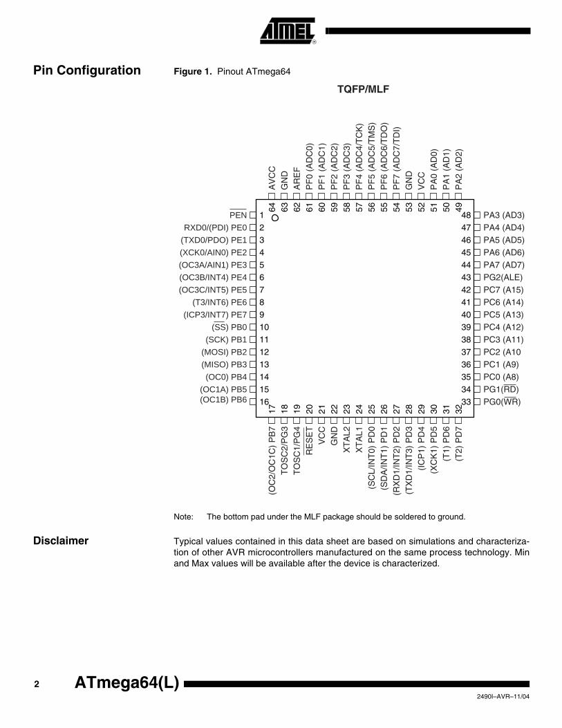
Pin Configuration Figure 1. Pinout ATmega64
Note: The bottom pad under the MLF package should be soldered to ground.
Disclaimer Typical values contained in this data sheet are based on simulations and characteriza-tion of other AVR microcontrollers manufactured on the same process technology. Minand Max values will be available after the device is characterized.
12345678910111213141516
48474645444342414039383736353433
PENRXD0/(PDI) PE0
(TXD0/PDO) PE1(XCK0/AIN0) PE2(OC3A/AIN1) PE3(OC3B/INT4) PE4(OC3C/INT5) PE5
(T3/INT6) PE6(ICP3/INT7) PE7
(SS) PB0(SCK) PB1
(MOSI) PB2(MISO) PB3(OC0) PB4
(OC1A) PB5(OC1B) PB6
PA3 (AD3)PA4 (AD4)PA5 (AD5)PA6 (AD6)PA7 (AD7)PG2(ALE)PC7 (A15)PC6 (A14)PC5 (A13)PC4 (A12)PC3 (A11)PC2 (A10PC1 (A9)PC0 (A8)PG1(RD)PG0(WR)
64 63 62 61 60 59 58 57 56 55 54 53 52 51 50 49
17 18 19 20 21 22 23 24 25 26 27 28 29 30 31 32
(OC
2/O
C1C
) P
B7
TO
SC
2/P
G3
TO
SC
1/P
G4
RE
SE
TV
CC
GN
DX
TA
L2X
TA
L1(S
CL/
INT
0) P
D0
(S
DA
/INT
1) P
D1
(RX
D1/
INT
2) P
D2
(TX
D1/
INT
3) P
D3
(IC
P1)
PD
4(X
CK
1) P
D5
(T1)
PD
6(T
2) P
D7
AV
CC
GN
DA
RE
FP
F0
(AD
C0)
PF
1 (A
DC
1)P
F2
(AD
C2)
PF
3 (A
DC
3)P
F4
(AD
C4/
TC
K)
PF
5 (A
DC
5/T
MS
)P
F6
(AD
C6/
TD
O)
PF
7 (A
DC
7/T
DI)
GN
DV
CC
PA
0 (A
D0)
P
A1
(AD
1)P
A2
(AD
2)
TQFP/MLF
2 ATmega64(L)2490I–AVR–11/04
ATmega64(L)
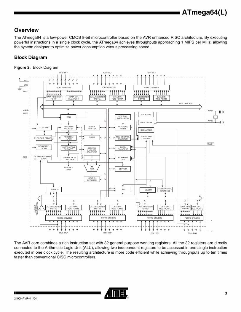
OverviewThe ATmega64 is a low-power CMOS 8-bit microcontroller based on the AVR enhanced RISC architecture. By executingpowerful instructions in a single clock cycle, the ATmega64 achieves throughputs approaching 1 MIPS per MHz, allowingthe system designer to optimize power consumption versus processing speed.
Block Diagram
Figure 2. Block Diagram
The AVR core combines a rich instruction set with 32 general purpose working registers. All the 32 registers are directlyconnected to the Arithmetic Logic Unit (ALU), allowing two independent registers to be accessed in one single instructionexecuted in one clock cycle. The resulting architecture is more code efficient while achieving throughputs up to ten timesfaster than conventional CISC microcontrollers.
PROGRAMCOUNTER
INTERNALOSCILLATOR
WATCHDOGTIMER
STACKPOINTER
PROGRAMFLASH
MCU CONTROLREGISTER
SRAM
GENERALPURPOSE
REGISTERS
INSTRUCTIONREGISTER
TIMER/COUNTERS
INSTRUCTIONDECODER
DATA DIR.REG. PORTB
DATA DIR.REG. PORTE
DATA DIR.REG. PORTA
DATA DIR.REG. PORTD
DATA REGISTERPORTB
DATA REGISTERPORTE
DATA REGISTERPORTA
DATA REGISTERPORTD
TIMING ANDCONTROL
OSCILLATOR
OSCILLATOR
INTERRUPTUNIT
EEPROM
SPIUSART0
STATUSREGISTER
Z
YX
ALU
PORTB DRIVERSPORTE DRIVERS
PORTA DRIVERSPORTF DRIVERS
PORTD DRIVERS
PORTC DRIVERS
PB0 - PB7PE0 - PE7
PA0 - PA7PF0 - PF7
RESET
VCC
AGND
GND
AREFXTAL1
XTAL2
CONTROLLINES
+ -
AN
ALO
GC
OM
PAR
AT
OR
PC0 - PC7
8-BIT DATA BUS
AVCC
USART1
CALIB. OSC
DATA DIR.REG. PORTC
DATA REGISTERPORTC
ON-CHIP DEBUG
JTAG TAP
PROGRAMMINGLOGICPEN
BOUNDARY- SCAN
DATA DIR.REG. PORTF
DATA REGISTERPORTF
ADC
PD0 - PD7
DATA DIR.REG. PORTG
DATA REG.PORTG
PORTG DRIVERS
PG0 - PG4
2-WIRE SERIALINTERFACE
32490I–AVR–11/04
The ATmega64 provides the following features: 64K bytes of In-System ProgrammableFlash with Read-While-Write capabilities, 2K bytes EEPROM, 4K bytes SRAM, 53 gen-eral purpose I/O lines, 32 general purpose working registers, Real Time Counter (RTC),four flexible Timer/Counters with compare modes and PWM, two USARTs, a byte ori-ented Two-wire Serial Interface, an 8-channel, 10-bit ADC with optional differential inputstage with programmable gain, programmable Watchdog Timer with internal Oscillator,an SPI serial port, IEEE std. 1149.1 compliant JTAG test interface, also used foraccessing the On-chip Debug system and programming, and six software selectablepower saving modes. The Idle mode stops the CPU while allowing the SRAM,Timer/Counters, SPI port, and interrupt system to continue functioning. The Power-down mode saves the register contents but freezes the Oscillator, disabling all otherchip functions until the next interrupt or Hardware Reset. In Power-save mode, the asyn-chronous timer continues to run, allowing the user to maintain a timer base while therest of the device is sleeping. The ADC Noise Reduction mode stops the CPU and allI/O modules except asynchronous timer and ADC, to minimize switching noise duringADC conversions. In Standby mode, the crystal/resonator Oscillator is running while therest of the device is sleeping. This allows very fast start-up combined with low powerconsumption. In Extended Standby mode, both the main Oscillator and the asynchro-nous timer continue to run.
The device is manufactured using Atmel’s high-density non-volatile memory technology.The On-chip ISP Flash allows the program memory to be reprogrammed In-Systemthrough an SPI serial interface, by a conventional non-volatile memory programmer, orby an On-chip Boot program running on the AVR core. The Boot Program can use anyinterface to download the Application Program in the Application Flash memory. Soft-ware in the Boot Flash section will continue to run while the Application Flash section isupdated, providing true Read-While-Write operation. By combining an 8-bit RISC CPUwith In-System Self-Programmable Flash on a monolithic chip, the Atmel ATmega64 isa powerful microcontroller that provides a highly-flexible and cost-effective solution tomany embedded control applications.
The ATmega64 AVR is supported with a full suite of program and system developmenttools including: C compilers, macro assemblers, program debugger/simulators, In-Cir-cuit Emulators, and evaluation kits.
ATmega103 and ATmega64 Compatibility
The ATmega64 is a highly complex microcontroller where the number of I/O locationssupersedes the 64 I/O location reserved in the AVR instruction set. To ensure backwardcompatibility with the ATmega103, all I/O locations present in ATmega103 have thesame location in ATmega64. Most additional I/O locations are added in an Extended I/Ospace starting from 0x60 to 0xFF (i.e., in the ATmega103 internal RAM space). Theselocation can be reached by using LD/LDS/LDD and ST/STS/STD instructions only, notby using IN and OUT instructions. The relocation of the internal RAM space may still bea problem for ATmega103 users. Also, the increased number of Interrupt Vectors mightbe a problem if the code uses absolute addresses. To solve these problems, anATmega103 compatibility mode can be selected by programming the fuse M103C. Inthis mode, none of the functions in the Extended I/O space are in use, so the internalRAM is located as in ATmega103. Also, the extended Interrupt Vectors are removed.
The ATmega64 is 100% pin compatible with ATmega103, and can replace theATmega103 on current printed circuit boards. The application notes “ReplacingATmega103 by ATmega128” and “Migration between ATmega64 and ATmega128”describes what the user should be aware of replacing the ATmega103 by anATmega128 or ATmega64.
4 ATmega64(L)2490I–AVR–11/04
ATmega64(L)
ATmega103 Compatibility Mode
By programming the M103C Fuse, the ATmega64 will be compatible with theATmega103 regards to RAM, I/O pins and Interrupt Vectors as described above. How-ever, some new features in ATmega64 are not available in this compatibility mode,these features are listed below:
• One USART instead of two, asynchronous mode only. Only the eight least significant bits of the Baud Rate Register is available.
• One 16 bits Timer/Counter with two compare registers instead of two 16 bits Timer/Counters with three compare registers.
• Two-wire serial interface is not supported.
• Port G serves alternate functions only (not a general I/O port).
• Port F serves as digital input only in addition to analog input to the ADC.
• Boot Loader capabilities is not supported.
• It is not possible to adjust the frequency of the internal calibrated RC Oscillator.
• The External Memory Interface can not release any Address pins for general I/O, neither configure different wait states to different External Memory Address sections.
• Only EXTRF and PORF exist in the MCUCSR Register.
• No timed sequence is required for Watchdog Timeout change.
• Only low-level external interrupts can be used on four of the eight External Interrupt sources.
• Port C is output only.
• USART has no FIFO buffer, so Data OverRun comes earlier.
• The user must have set unused I/O bits to 0 in ATmega103 programs.
Pin Descriptions
VCC Digital supply voltage.
GND Ground.
Port A (PA7..PA0) Port A is an 8-bit bi-directional I/O port with internal pull-up resistors (selected for eachbit). The Port A output buffers have symmetrical drive characteristics with both high sinkand source capability. As inputs, Port A pins that are externally pulled low will sourcecurrent if the pull-up resistors are activated. The Port A pins are tri-stated when a resetcondition becomes active, even if the clock is not running.
Port A also serves the functions of various special features of the ATmega64 as listedon page 72.
Port B (PB7..PB0) Port B is an 8-bit bi-directional I/O port with internal pull-up resistors (selected for eachbit). The Port B output buffers have symmetrical drive characteristics with both high sinkand source capability. As inputs, Port B pins that are externally pulled low will sourcecurrent if the pull-up resistors are activated. The Port B pins are tri-stated when a resetcondition becomes active, even if the clock is not running.
Port B also serves the functions of various special features of the ATmega64 as listedon page 73.
52490I–AVR–11/04
Port C (PC7..PC0) Port C is an 8-bit bi-directional I/O port with internal pull-up resistors (selected for eachbit). The Port C output buffers have symmetrical drive characteristics with both high sinkand source capability. As inputs, Port C pins that are externally pulled low will sourcecurrent if the pull-up resistors are activated. The Port C pins are tri-stated when a resetcondition becomes active, even if the clock is not running.
Port C also serves the functions of special features of the ATmega64 as listed on page76. In ATmega103 compatibility mode, Port C is output only, and the port C pins are nottri-stated when a reset condition becomes active.
Port D (PD7..PD0) Port D is an 8-bit bi-directional I/O port with internal pull-up resistors (selected for eachbit). The Port D output buffers have symmetrical drive characteristics with both high sinkand source capability. As inputs, Port D pins that are externally pulled low will sourcecurrent if the pull-up resistors are activated. The Port D pins are tri-stated when a resetcondition becomes active, even if the clock is not running.
Port D also serves the functions of various special features of the ATmega64 as listedon page 77.
Port E (PE7..PE0) Port E is an 8-bit bi-directional I/O port with internal pull-up resistors (selected for eachbit). The Port E output buffers have symmetrical drive characteristics with both high sinkand source capability. As inputs, Port E pins that are externally pulled low will sourcecurrent if the pull-up resistors are activated. The Port E pins are tri-stated when a resetcondition becomes active, even if the clock is not running.
Port E also serves the functions of various special features of the ATmega64 as listedon page 80.
Port F (PF7..PF0) Port F serves as the analog inputs to the A/D Converter.
Port F also serves as an 8-bit bi-directional I/O port, if the A/D Converter is not used.Port pins can provide internal pull-up resistors (selected for each bit). The Port F outputbuffers have symmetrical drive characteristics with both high sink and source capability.As inputs, Port F pins that are externally pulled low will source current if the pull-upresistors are activated. The Port F pins are tri-stated when a reset condition becomesactive, even if the clock is not running. If the JTAG interface is enabled, the pull-up resis-tors on pins PF7(TDI), PF5(TMS) and PF4(TCK) will be activated even if a reset occurs.
The TDO pin is tri-stated unless TAP states that shift out data are entered.
Port F also serves the functions of the JTAG interface.
In ATmega103 compatibility mode, Port F is an input port only.
Port G (PG4..PG0) Port G is a 5-bit bi-directional I/O port with internal pull-up resistors (selected for eachbit). The Port G output buffers have symmetrical drive characteristics with both high sinkand source capability. As inputs, Port G pins that are externally pulled low will sourcecurrent if the pull-up resistors are activated. The Port G pins are tri-stated when a resetcondition becomes active, even if the clock is not running.
Port G also serves the functions of various special features.
In ATmega103 compatibility mode, these pins only serves as strobes signals to theexternal memory as well as input to the 32 kHz Oscillator, and the pins are initialized toPG0 = 1, PG1 = 1, and PG2 = 0 asynchronously when a reset condition becomesactive, even if the clock is not running. PG3 and PG4 are Oscillator pins.
6 ATmega64(L)2490I–AVR–11/04
ATmega64(L)
RESET Reset input. A low level on this pin for longer than the minimum pulse length will gener-ate a reset, even if the clock is not running. The minimum pulse length is given in Table19 on page 51. Shorter pulses are not guaranteed to generate a reset.
XTAL1 Input to the inverting Oscillator amplifier and input to the internal clock operating circuit.
XTAL2 Output from the inverting Oscillator amplifier.
AVCC AVCC is the supply voltage pin for Port F and the A/D Converter. It should be externallyconnected to VCC, even if the ADC is not used. If the ADC is used, it should be con-nected to VCC through a low-pass filter.
AREF AREF is the analog reference pin for the A/D Converter.
PEN This is a programming enable pin for the SPI Serial Programming mode. By holding thispin low during a Power-on Reset, the device will enter the SPI Serial Programmingmode. PEN has no function during normal operation.
About Code Examples
This datasheet contains simple code examples that briefly show how to use variousparts of the device. These code examples assume that the part specific header file isincluded before compilation. Be aware that not all C compiler vendors include bit defini-tions in the header files and interrupt handling in C is compiler dependent. Pleaseconfirm with the C compiler documentation for more details.
72490I–AVR–11/04
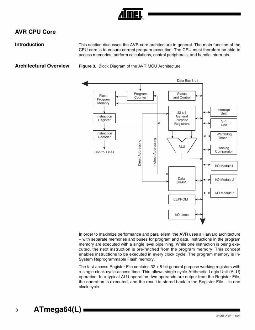
AVR CPU Core
Introduction This section discusses the AVR core architecture in general. The main function of theCPU core is to ensure correct program execution. The CPU must therefore be able toaccess memories, perform calculations, control peripherals, and handle interrupts.
Architectural Overview Figure 3. Block Diagram of the AVR MCU Architecture
In order to maximize performance and parallelism, the AVR uses a Harvard architecture– with separate memories and buses for program and data. Instructions in the programmemory are executed with a single level pipelining. While one instruction is being exe-cuted, the next instruction is pre-fetched from the program memory. This conceptenables instructions to be executed in every clock cycle. The program memory is In-System Reprogrammable Flash memory.
The fast-access Register File contains 32 x 8-bit general purpose working registers witha single clock cycle access time. This allows single-cycle Arithmetic Logic Unit (ALU)operation. In a typical ALU operation, two operands are output from the Register File,the operation is executed, and the result is stored back in the Register File – in oneclock cycle.
FlashProgramMemory
InstructionRegister
InstructionDecoder
ProgramCounter
Control Lines
32 x 8GeneralPurpose
Registrers
ALU
Statusand Control
I/O Lines
EEPROM
Data Bus 8-bit
DataSRAM
Dire
ct A
ddre
ssin
g
Indi
rect
Add
ress
ing
InterruptUnit
SPIUnit
WatchdogTimer
AnalogComparator
I/O Module 2
I/O Module1
I/O Module n
8 ATmega64(L)2490I–AVR–11/04
ATmega64(L)
Six of the 32 registers can be used as three 16-bit indirect address register pointers forData Space addressing – enabling efficient address calculations. One of the theseaddress pointers can also be used as an address pointer for look up tables in Flash pro-gram memory. These added function registers are the 16-bit X-, Y-, and Z-register,described later in this section.
The ALU supports arithmetic and logic operations between registers or between a con-stant and a register. Single register operations can also be executed in the ALU. Afteran arithmetic operation, the Status Register is updated to reflect information about theresult of the operation.
Program flow is provided by conditional and unconditional jump and call instructions,able to directly address the whole address space. Most AVR instructions have a single16-bit word format. Every program memory address contains a 16- or 32-bit instruction.
Program Flash memory space is divided in two sections, the Boot program section andthe Application program section. Both sections have dedicated Lock bits for write andread/write protection. The SPM instruction that writes into the Application Flash memorysection must reside in the Boot program section.
During interrupts and subroutine calls, the return address Program Counter (PC) isstored on the Stack. The Stack is effectively allocated in the general data SRAM, andconsequently the Stack size is only limited by the total SRAM size and the usage of theSRAM. All user programs must initialize the SP in the reset routine (before subroutinesor interrupts are executed). The Stack Pointer SP is read/write accessible in the I/Ospace. The data SRAM can easily be accessed through the five different addressingmodes supported in the AVR architecture.
The memory spaces in the AVR architecture are all linear and regular memory maps.
A flexible interrupt module has its control registers in the I/O space with an additionalGlobal Interrupt Enable bit in the Status Register. All interrupts have a separate InterruptVector in the Interrupt Vector table. The interrupts have priority in accordance with theirInterrupt Vector position. The lower the Interrupt Vector address, the higher the priority.
The I/O memory space contains 64 addresses which can be accessed directly, or as theData Space locations following those of the Register File, 0x20 - 0x5F. In addition, theATmega64 has Extended I/O space from 0x60 - 0xFF in SRAM where only theST/STS/STD and LD/LDS/LDD instructions can be used.
ALU – Arithmetic Logic Unit
The high-performance AVR ALU operates in direct connection with all the 32 generalpurpose working registers. Within a single clock cycle, arithmetic operations betweengeneral purpose registers or between a register and an immediate are executed. TheALU operations are divided into three main categories – arithmetic, logical, and bit-func-tions. Some implementations of the architecture also provide a powerful multipliersupporting both signed/unsigned multiplication and fractional format. See the “Instruc-tion Set” section for a detailed description.
92490I–AVR–11/04
Status Register The Status Register contains information about the result of the most recently executedarithmetic instruction. This information can be used for altering program flow in order toperform conditional operations. Note that the Status Register is updated after all ALUoperations, as specified in the Instruction Set Reference. This will in many casesremove the need for using the dedicated compare instructions, resulting in faster andmore compact code.
The Status Register is not automatically stored when entering an interrupt routine andrestored when returning from an interrupt. This must be handled by software.
The AVR Status Register – SREG – is defined as:
• Bit 7 – I: Global Interrupt Enable
The Global Interrupt Enable bit must be set for the interrupts to be enabled. The individ-ual interrupt enable control is then performed in separate control registers. If the GlobalInterrupt Enable Register is cleared, none of the interrupts are enabled independent ofthe individual interrupt enable settings. The I-bit is cleared by hardware after an interrupthas occurred, and is set by the RETI instruction to enable subsequent interrupts. The I-bit can also be set and cleared in software with the SEI and CLI instructions, asdescribed in the instruction set reference.
• Bit 6 – T: Bit Copy Storage
The Bit Copy instructions BLD (Bit LoaD) and BST (Bit STore) use the T-bit as source ordestination for the operated bit. A bit from a register in the Register File can be copiedinto T by the BST instruction, and a bit in T can be copied into a bit in a register in theRegister File by the BLD instruction.
• Bit 5 – H: Half Carry Flag
The Half Carry Flag H indicates a Half Carry in some arithmetic operations. Half Carry isuseful in BCD arithmetic. See the “Instruction Set Description” for detailed information.
• Bit 4 – S: Sign Bit, S = N ⊕ V
The S-bit is always an exclusive or between the Negative Flag N and the Two’s Comple-ment Overflow Flag V. See the “Instruction Set Description” for detailed information.
• Bit 3 – V: Two’s Complement Overflow Flag
The Two’s Complement Overflow Flag V supports two’s complement arithmetics. Seethe “Instruction Set Description” for detailed information.
• Bit 2 – N: Negative Flag
The Negative Flag N indicates a negative result in an arithmetic or logic operation. Seethe “Instruction Set Description” for detailed information.
• Bit 1 – Z: Zero Flag
The Zero Flag Z indicates a zero result in an arithmetic or logic operation. See the“Instruction Set Description” for detailed information.
Bit 7 6 5 4 3 2 1 0
I T H S V N Z C SREGRead/Write R/W R/W R/W R/W R/W R/W R/W R/W
Initial Value 0 0 0 0 0 0 0 0
10 ATmega64(L)2490I–AVR–11/04
ATmega64(L)
• Bit 0 – C: Carry Flag
The Carry Flag C indicates a carry in an arithmetic or logic operation. See the “Instruc-tion Set Description” for detailed information.
General Purpose Register File
The Register File is optimized for the AVR Enhanced RISC instruction set. In order toachieve the required performance and flexibility, the following input/output schemes aresupported by the Register File:
• One 8-bit output operand and one 8-bit result input.
• Two 8-bit output operands and one 8-bit result input.
• Two 8-bit output operands and one 16-bit result input.
• One 16-bit output operand and one 16-bit result input.
Figure 4 shows the structure of the 32 general purpose working registers in the CPU.
Figure 4. AVR CPU General Purpose Working Registers
Most of the instructions operating on the Register File have direct access to all registers,and most of them are single cycle instructions.
As shown in Figure 4, each register is also assigned a data memory address, mappingthem directly into the first 32 locations of the user data space. Although not being physi-cally implemented as SRAM locations, this memory organization provides greatflexibility in access of the registers, as the X-, Y-, and Z-pointer registers can be set toindex any register in the file.
7 0 Addr.
R0 0x00
R1 0x01
R2 0x02
…
R13 0x0D
General R14 0x0E
Purpose R15 0x0F
Working R16 0x10
Registers R17 0x11
…
R26 0x1A X-register Low Byte
R27 0x1B X-register High Byte
R28 0x1C Y-register Low Byte
R29 0x1D Y-register High Byte
R30 0x1E Z-register Low Byte
R31 0x1F Z-register High Byte
112490I–AVR–11/04
X-, Y-, and Z-register The registers R26..R31 have some added functions to their general purpose usage.These registers are 16-bit address pointers for indirect addressing of the data space.The three indirect address registers X, Y, and Z are defined as described in Figure 5.
Figure 5. The X-, Y-, and Z-Registers
In the different addressing modes these address registers have functions as fixed dis-placement, automatic increment, and automatic decrement (see the Instruction SetReference for details).
Stack Pointer The Stack is mainly used for storing temporary data, for storing local variables and forstoring return addresses after interrupts and subroutine calls. The Stack Pointer Regis-ter always points to the top of the Stack. Note that the Stack is implemented as growingfrom higher memory locations to lower memory locations. This implies that a StackPUSH command decreases the Stack Pointer. If software reads the Program Counterfrom the Stack after a call or an interrupt, unused bits (bit 15) should be masked out.
The Stack Pointer points to the data SRAM Stack area where the subroutine and inter-rupt Stacks are located. This Stack space in the data SRAM must be defined by theprogram before any subroutine calls are executed or interrupts are enabled. The StackPointer must be set to point above 0x60. The Stack Pointer is decremented by onewhen data is pushed onto the Stack with the PUSH instruction, and it is decremented bytwo when the return address is pushed onto the Stack with subroutine call or interrupt.The Stack Pointer is incremented by one when data is popped from the Stack with thePOP instruction, and it is incremented by two when data is popped from the Stack withreturn from subroutine RET or return from interrupt RETI.
The AVR Stack Pointer is implemented as two 8-bit registers in the I/O space. The num-ber of bits actually used is implementation dependent. Note that the data space in someimplementations of the AVR architecture is so small that only SPL is needed. In thiscase, the SPH Register will not be present.
15 XH XL 0
X - register 7 0 7 0
R27 (0x1B) R26 (0x1A)
15 YH YL 0
Y - register 7 0 7 0
R29 (0x1D) R28 (0x1C)
15 ZH ZL 0
Z - register 7 0 7 0
R31 (0x1F) R30 (0x1E)
Bit 15 14 13 12 11 10 9 8
SP15 SP14 SP13 SP12 SP11 SP10 SP9 SP8 SPHSP7 SP6 SP5 SP4 SP3 SP2 SP1 SP0 SPL
7 6 5 4 3 2 1 0
Read/Write R/W R/W R/W R/W R/W R/W R/W R/W
R/W R/W R/W R/W R/W R/W R/W R/W
Initial Value 0 0 0 0 0 0 0 0
0 0 0 0 0 0 0 0
12 ATmega64(L)2490I–AVR–11/04
ATmega64(L)
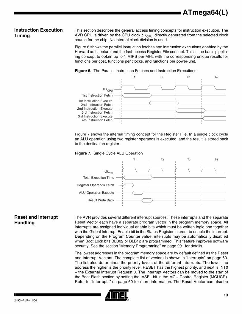
Instruction Execution Timing
This section describes the general access timing concepts for instruction execution. TheAVR CPU is driven by the CPU clock clkCPU, directly generated from the selected clocksource for the chip. No internal clock division is used.
Figure 6 shows the parallel instruction fetches and instruction executions enabled by theHarvard architecture and the fast-access Register File concept. This is the basic pipelin-ing concept to obtain up to 1 MIPS per MHz with the corresponding unique results forfunctions per cost, functions per clocks, and functions per power-unit.
Figure 6. The Parallel Instruction Fetches and Instruction Executions
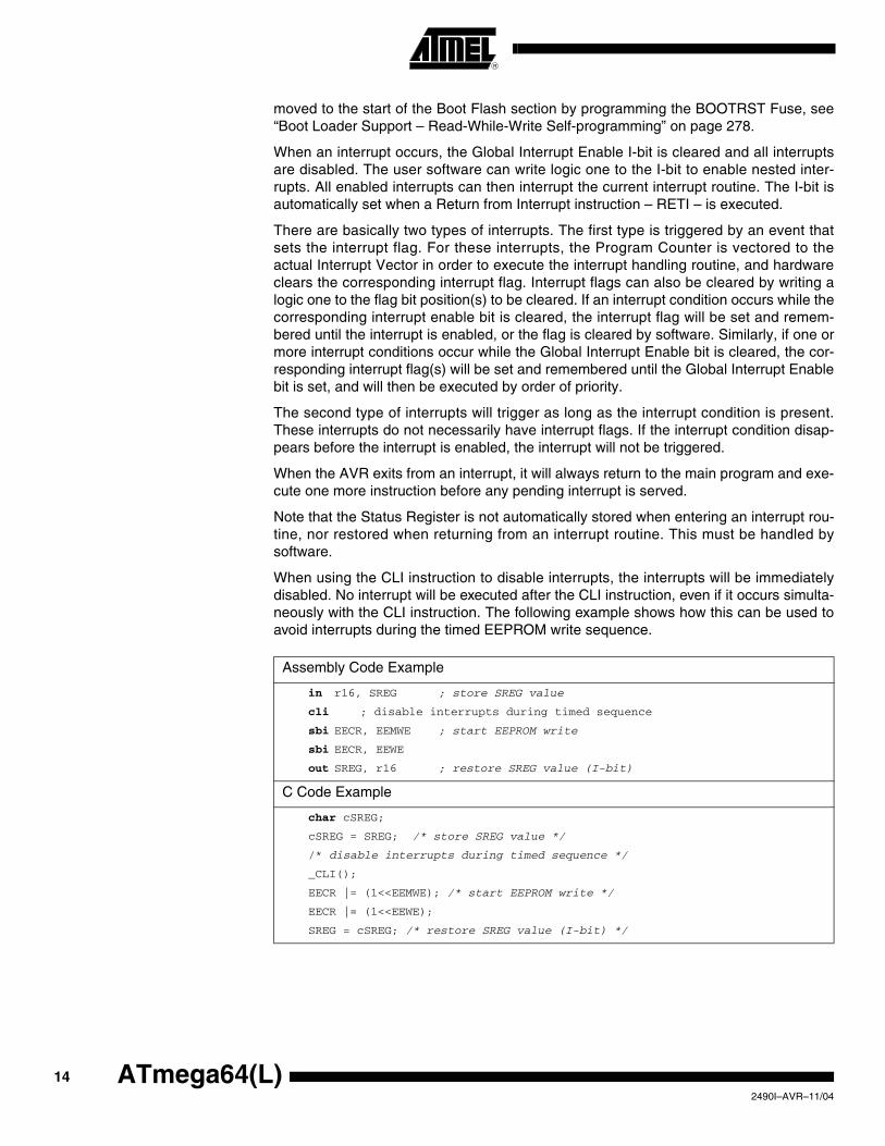
Figure 7 shows the internal timing concept for the Register File. In a single clock cyclean ALU operation using two register operands is executed, and the result is stored backto the destination register.
Figure 7. Single Cycle ALU Operation
Reset and Interrupt Handling
The AVR provides several different interrupt sources. These interrupts and the separateReset Vector each have a separate program vector in the program memory space. Allinterrupts are assigned individual enable bits which must be written logic one togetherwith the Global Interrupt Enable bit in the Status Register in order to enable the interrupt.Depending on the Program Counter value, interrupts may be automatically disabledwhen Boot Lock bits BLB02 or BLB12 are programmed. This feature improves softwaresecurity. See the section “Memory Programming” on page 291 for details.
The lowest addresses in the program memory space are by default defined as the Resetand Interrupt Vectors. The complete list of vectors is shown in “Interrupts” on page 60.The list also determines the priority levels of the different interrupts. The lower theaddress the higher is the priority level. RESET has the highest priority, and next is INT0– the External Interrupt Request 0. The Interrupt Vectors can be moved to the start ofthe Boot Flash section by setting the IVSEL bit in the MCU Control Register (MCUCR).Refer to “Interrupts” on page 60 for more information. The Reset Vector can also be
clk
1st Instruction Fetch
1st Instruction Execute2nd Instruction Fetch
2nd Instruction Execute3rd Instruction Fetch
3rd Instruction Execute4th Instruction Fetch
T1 T2 T3 T4
CPU
Total Execution Time
Register Operands Fetch
ALU Operation Execute
Result Write Back
T1 T2 T3 T4
clkCPU
132490I–AVR–11/04
moved to the start of the Boot Flash section by programming the BOOTRST Fuse, see“Boot Loader Support – Read-While-Write Self-programming” on page 278.
When an interrupt occurs, the Global Interrupt Enable I-bit is cleared and all interruptsare disabled. The user software can write logic one to the I-bit to enable nested inter-rupts. All enabled interrupts can then interrupt the current interrupt routine. The I-bit isautomatically set when a Return from Interrupt instruction – RETI – is executed.
There are basically two types of interrupts. The first type is triggered by an event thatsets the interrupt flag. For these interrupts, the Program Counter is vectored to theactual Interrupt Vector in order to execute the interrupt handling routine, and hardwareclears the corresponding interrupt flag. Interrupt flags can also be cleared by writing alogic one to the flag bit position(s) to be cleared. If an interrupt condition occurs while thecorresponding interrupt enable bit is cleared, the interrupt flag will be set and remem-bered until the interrupt is enabled, or the flag is cleared by software. Similarly, if one ormore interrupt conditions occur while the Global Interrupt Enable bit is cleared, the cor-responding interrupt flag(s) will be set and remembered until the Global Interrupt Enablebit is set, and will then be executed by order of priority.
The second type of interrupts will trigger as long as the interrupt condition is present.These interrupts do not necessarily have interrupt flags. If the interrupt condition disap-pears before the interrupt is enabled, the interrupt will not be triggered.
When the AVR exits from an interrupt, it will always return to the main program and exe-cute one more instruction before any pending interrupt is served.
Note that the Status Register is not automatically stored when entering an interrupt rou-tine, nor restored when returning from an interrupt routine. This must be handled bysoftware.
When using the CLI instruction to disable interrupts, the interrupts will be immediatelydisabled. No interrupt will be executed after the CLI instruction, even if it occurs simulta-neously with the CLI instruction. The following example shows how this can be used toavoid interrupts during the timed EEPROM write sequence.
Assembly Code Example
in r16, SREG ; store SREG value
cli ; disable interrupts during timed sequence
sbi EECR, EEMWE ; start EEPROM write
sbi EECR, EEWE
out SREG, r16 ; restore SREG value (I-bit)
C Code Example
char cSREG;
cSREG = SREG; /* store SREG value */
/* disable interrupts during timed sequence */
_CLI();
EECR |= (1<<EEMWE); /* start EEPROM write */
EECR |= (1<<EEWE);
SREG = cSREG; /* restore SREG value (I-bit) */
14 ATmega64(L)2490I–AVR–11/04
ATmega64(L)
When using the SEI instruction to enable interrupts, the instruction following SEI will beexecuted before any pending interrupts, as shown in this example.
Interrupt Response Time The interrupt execution response for all the enabled AVR interrupts is four clock cyclesminimum. After four clock cycles the program vector address for the actual interrupthandling routine is executed. During this four clock cycle period, the Program Counter ispushed onto the Stack. The vector is normally a jump to the interrupt routine, and thisjump takes three clock cycles. If an interrupt occurs during execution of a multi-cycleinstruction, this instruction is completed before the interrupt is served. If an interruptoccurs when the MCU is in sleep mode, the interrupt execution response time isincreased by four clock cycles. This increase comes in addition to the start-up time fromthe selected sleep mode.
A return from an interrupt handling routine takes four clock cycles. During these fourclock cycles, the Program Counter (two bytes) is popped back from the Stack, the StackPointer is incremented by two, and the I-bit in SREG is set.
Assembly Code Example
sei ; set global interrupt enable
sleep ; enter sleep, waiting for interrupt
; note: will enter sleep before any pending
; interrupt(s)
C Code Example
_SEI(); /* set global interrupt enable */
_SLEEP(); /* enter sleep, waiting for interrupt */
/* note: will enter sleep before any pending interrupt(s) */
152490I–AVR–11/04
AVR ATmega64
MemoriesThis section describes the different memories in the ATmega64. The AVR architecturehas two main memory spaces, the Data Memory and the Program Memory space. Inaddition, the ATmega64 features an EEPROM Memory for data storage. All three mem-ory spaces are linear and regular.
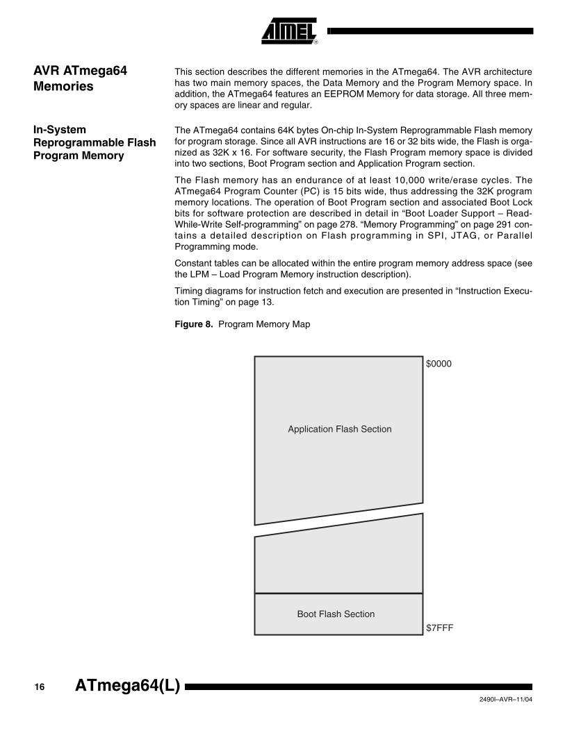
In-System Reprogrammable Flash Program Memory
The ATmega64 contains 64K bytes On-chip In-System Reprogrammable Flash memoryfor program storage. Since all AVR instructions are 16 or 32 bits wide, the Flash is orga-nized as 32K x 16. For software security, the Flash Program memory space is dividedinto two sections, Boot Program section and Application Program section.
The Flash memory has an endurance of at least 10,000 write/erase cycles. TheATmega64 Program Counter (PC) is 15 bits wide, thus addressing the 32K programmemory locations. The operation of Boot Program section and associated Boot Lockbits for software protection are described in detail in “Boot Loader Support – Read-While-Write Self-programming” on page 278. “Memory Programming” on page 291 con-tains a detailed description on Flash programming in SPI, JTAG, or ParallelProgramming mode.
Constant tables can be allocated within the entire program memory address space (seethe LPM – Load Program Memory instruction description).
Timing diagrams for instruction fetch and execution are presented in “Instruction Execu-tion Timing” on page 13.
Figure 8. Program Memory Map
$0000
$7FFF
Application Flash Section
Boot Flash Section
16 ATmega64(L)2490I–AVR–11/04
ATmega64(L)
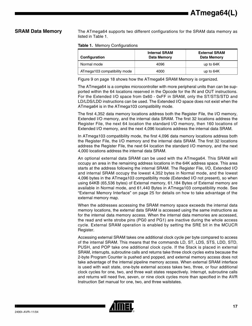
SRAM Data Memory The ATmega64 supports two different configurations for the SRAM data memory aslisted in Table 1.
Figure 9 on page 18 shows how the ATmega64 SRAM Memory is organized.
The ATmega64 is a complex microcontroller with more peripheral units than can be sup-ported within the 64 locations reserved in the Opcode for the IN and OUT instructions.For the Extended I/O space from 0x60 - 0xFF in SRAM, only the ST/STS/STD andLD/LDS/LDD instructions can be used. The Extended I/O space does not exist when theATmega64 is in the ATmega103 compatibility mode.
The first 4,352 data memory locations address both the Register File, the I/O memory,Extended I/O memory, and the internal data SRAM. The first 32 locations address theRegister File, the next 64 location the standard I/O memory, then 160 locations ofExtended I/O memory, and the next 4,096 locations address the internal data SRAM.
In ATmega103 compatibility mode, the first 4,096 data memory locations address boththe Register File, the I/O memory and the internal data SRAM. The first 32 locationsaddress the Register File, the next 64 location the standard I/O memory, and the next4,000 locations address the internal data SRAM.
An optional external data SRAM can be used with the ATmega64. This SRAM willoccupy an area in the remaining address locations in the 64K address space. This areastarts at the address following the internal SRAM. The Register File, I/O, Extended I/Oand internal SRAM occupy the lowest 4,352 bytes in Normal mode, and the lowest4,096 bytes in the ATmega103 compatibility mode (Extended I/O not present), so whenusing 64KB (65,536 bytes) of External memory, 61,184 Bytes of External memory areavailable in Normal mode, and 61,440 Bytes in ATmega103 compatibility mode. See“External Memory Interface” on page 25 for details on how to take advantage of theexternal memory map.
When the addresses accessing the SRAM memory space exceeds the internal datamemory locations, the external data SRAM is accessed using the same instructions asfor the internal data memory access. When the internal data memories are accessed,the read and write strobe pins (PG0 and PG1) are inactive during the whole accesscycle. External SRAM operation is enabled by setting the SRE bit in the MCUCRRegister.
Accessing external SRAM takes one additional clock cycle per byte compared to accessof the internal SRAM. This means that the commands LD, ST, LDS, STS, LDD, STD,PUSH, and POP take one additional clock cycle. If the Stack is placed in externalSRAM, interrupts, subroutine calls and returns take three clock cycles extra because the2-byte Program Counter is pushed and popped, and external memory access does nottake advantage of the internal pipeline memory access. When external SRAM interfaceis used with wait state, one-byte external access takes two, three, or four additionalclock cycles for one, two, and three wait states respectively. Interrupt, subroutine callsand returns will need five, seven, or nine clock cycles more than specified in the AVRInstruction Set manual for one, two, and three waitstates.
Table 1. Memory Configurations
ConfigurationInternal SRAM Data Memory
External SRAM Data Memory
Normal mode 4096 up to 64K
ATmega103 compatibility mode 4000 up to 64K
172490I–AVR–11/04
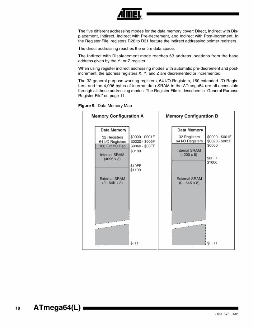
The five different addressing modes for the data memory cover: Direct, Indirect with Dis-placement, Indirect, Indirect with Pre-decrement, and Indirect with Post-increment. Inthe Register File, registers R26 to R31 feature the indirect addressing pointer registers.
The direct addressing reaches the entire data space.
The Indirect with Displacement mode reaches 63 address locations from the baseaddress given by the Y- or Z-register.
When using register indirect addressing modes with automatic pre-decrement and post-increment, the address registers X, Y, and Z are decremented or incremented.
The 32 general purpose working registers, 64 I/O Registers, 160 extended I/O Regis-ters, and the 4,096 bytes of internal data SRAM in the ATmega64 are all accessiblethrough all these addressing modes. The Register File is described in “General PurposeRegister File” on page 11.
Figure 9. Data Memory Map
Memory Configuration B
32 Registers64 I/O Registers
Internal SRAM(4000 x 8)
$0000 - $001F$0020 - $005F
$1000$0FFF
$FFFF
$0060
Data Memory
External SRAM(0 - 64K x 8)
Memory Configuration A
32 Registers64 I/O Registers
Internal SRAM(4096 x 8)
$0000 - $001F$0020 - $005F
$1100$10FF
$FFFF
$0060 - $00FF
Data Memory
External SRAM(0 - 64K x 8)
160 Ext I/O Reg.$0100
18 ATmega64(L)2490I–AVR–11/04
ATmega64(L)
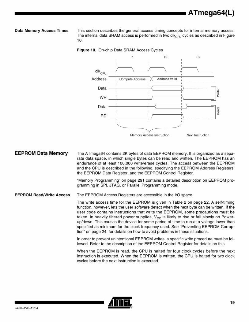
Data Memory Access Times This section describes the general access timing concepts for internal memory access.The internal data SRAM access is performed in two clkCPU cycles as described in Figure10.
Figure 10. On-chip Data SRAM Access Cycles
EEPROM Data Memory The ATmega64 contains 2K bytes of data EEPROM memory. It is organized as a sepa-rate data space, in which single bytes can be read and written. The EEPROM has anendurance of at least 100,000 write/erase cycles. The access between the EEPROMand the CPU is described in the following, specifying the EEPROM Address Registers,the EEPROM Data Register, and the EEPROM Control Register.
“Memory Programming” on page 291 contains a detailed description on EEPROM pro-gramming in SPI, JTAG, or Parallel Programming mode.
EEPROM Read/Write Access The EEPROM Access Registers are accessible in the I/O space.
The write access time for the EEPROM is given in Table 2 on page 22. A self-timingfunction, however, lets the user software detect when the next byte can be written. If theuser code contains instructions that write the EEPROM, some precautions must betaken. In heavily filtered power supplies, VCC is likely to rise or fall slowly on Power-up/down. This causes the device for some period of time to run at a voltage lower thanspecified as minimum for the clock frequency used. See “Preventing EEPROM Corrup-tion” on page 24. for details on how to avoid problems in these situations.
In order to prevent unintentional EEPROM writes, a specific write procedure must be fol-lowed. Refer to the description of the EEPROM Control Register for details on this.
When the EEPROM is read, the CPU is halted for four clock cycles before the nextinstruction is executed. When the EEPROM is written, the CPU is halted for two clockcycles before the next instruction is executed.
clk
WR
RD
Data
Data
Address Address Valid
T1 T2 T3
Compute Address
Rea
dW
rite
CPU
Memory Access Instruction Next Instruction
192490I–AVR–11/04
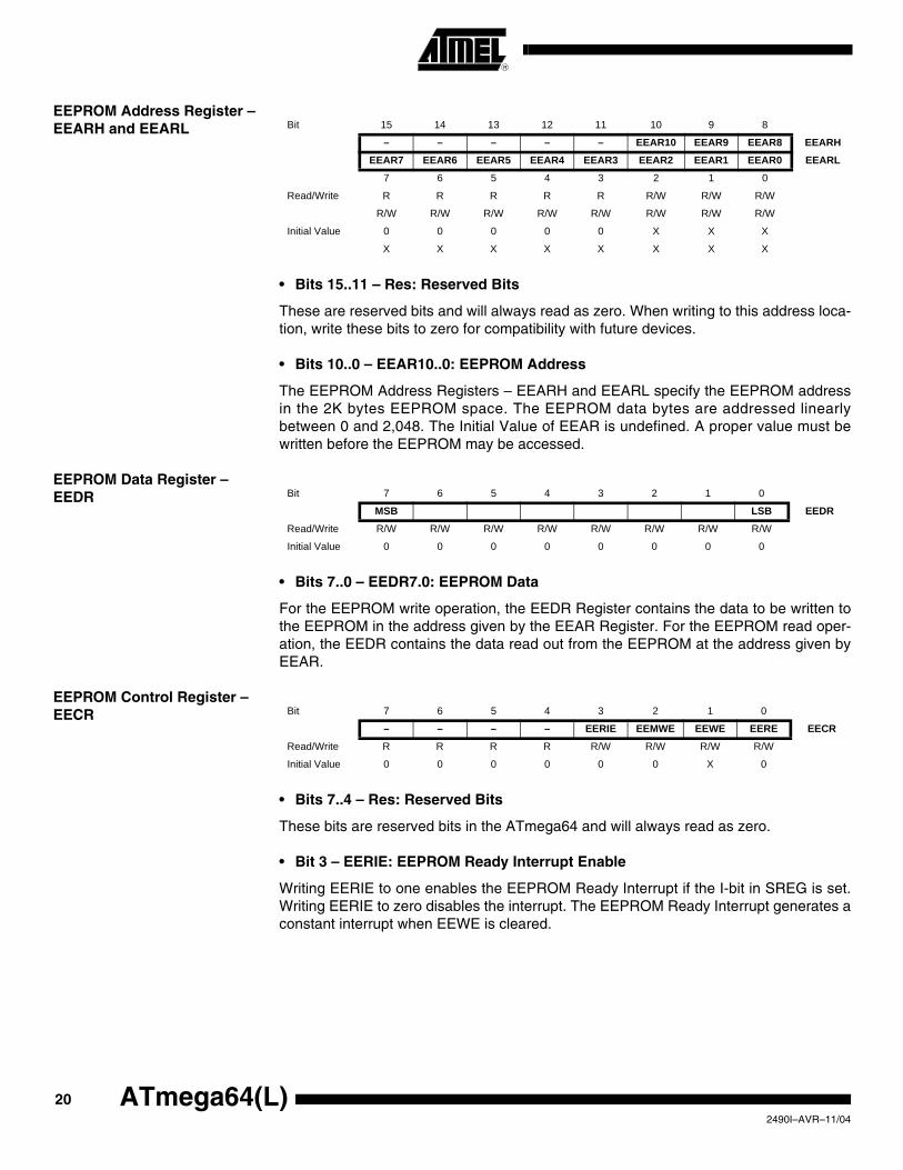
EEPROM Address Register – EEARH and EEARL
• Bits 15..11 – Res: Reserved Bits
These are reserved bits and will always read as zero. When writing to this address loca-tion, write these bits to zero for compatibility with future devices.
• Bits 10..0 – EEAR10..0: EEPROM Address
The EEPROM Address Registers – EEARH and EEARL specify the EEPROM addressin the 2K bytes EEPROM space. The EEPROM data bytes are addressed linearlybetween 0 and 2,048. The Initial Value of EEAR is undefined. A proper value must bewritten before the EEPROM may be accessed.
EEPROM Data Register – EEDR
• Bits 7..0 – EEDR7.0: EEPROM Data
For the EEPROM write operation, the EEDR Register contains the data to be written tothe EEPROM in the address given by the EEAR Register. For the EEPROM read oper-ation, the EEDR contains the data read out from the EEPROM at the address given byEEAR.
EEPROM Control Register – EECR
• Bits 7..4 – Res: Reserved Bits
These bits are reserved bits in the ATmega64 and will always read as zero.
• Bit 3 – EERIE: EEPROM Ready Interrupt Enable
Writing EERIE to one enables the EEPROM Ready Interrupt if the I-bit in SREG is set.Writing EERIE to zero disables the interrupt. The EEPROM Ready Interrupt generates aconstant interrupt when EEWE is cleared.
Bit 15 14 13 12 11 10 9 8
– – – – – EEAR10 EEAR9 EEAR8 EEARHEEAR7 EEAR6 EEAR5 EEAR4 EEAR3 EEAR2 EEAR1 EEAR0 EEARL
7 6 5 4 3 2 1 0
Read/Write R R R R R R/W R/W R/W
R/W R/W R/W R/W R/W R/W R/W R/W
Initial Value 0 0 0 0 0 X X X
X X X X X X X X
Bit 7 6 5 4 3 2 1 0
MSB LSB EEDRRead/Write R/W R/W R/W R/W R/W R/W R/W R/W
Initial Value 0 0 0 0 0 0 0 0
Bit 7 6 5 4 3 2 1 0
– – – – EERIE EEMWE EEWE EERE EECRRead/Write R R R R R/W R/W R/W R/W
Initial Value 0 0 0 0 0 0 X 0
20 ATmega64(L)2490I–AVR–11/04
ATmega64(L)
• Bit 2 – EEMWE: EEPROM Master Write Enable
The EEMWE bit determines whether setting EEWE to one causes the EEPROM to bewritten. When EEMWE is written to one, writing EEWE to one within four clock cycleswill write data to the EEPROM at the selected address. If EEMWE is zero, writing EEWEto one will have no effect. When EEMWE has been written to one by software, hardwareclears the bit to zero after four clock cycles. See the description of the EEWE bit for anEEPROM write procedure.
• Bit 1 – EEWE: EEPROM Write Enable
The EEPROM Write Enable Signal EEWE is the write strobe to the EEPROM. Whenaddress and data are correctly set up, the EEWE bit must be set to write the value intothe EEPROM. The EEMWE bit must be set when the logical one is written to EEWE,otherwise no EEPROM write takes place. The following procedure should be followedwhen writing the EEPROM (the order of steps 3 and 4 is not essential):
1. Wait until EEWE becomes zero.
2. Wait until SPMEN in SPMCSR becomes zero.
3. Write new EEPROM address to EEAR (optional).
4. Write new EEPROM data to EEDR (optional).
5. Write a logical one to the EEMWE bit while writing a zero to EEWE in EECR.
6. Within four clock cycles after setting EEMWE, write a logical one to EEWE.
The EEPROM can not be programmed during a CPU write to the Flash memory. Thesoftware must check that the Flash programming is completed before initiating a newEEPROM write. Step 2 is only relevant if the software contains a Boot Loader allowingthe CPU to program the Flash. If the Flash is never being updated by the CPU, step 2can be omitted. See “Boot Loader Support – Read-While-Write Self-programming” onpage 278 for details about Boot programming.
Caution: An interrupt between step 5 and step 6 will make the write cycle fail, since theEEPROM Master Write Enable will time-out. If an interrupt routine accessing theEEPROM is interrupting another EEPROM access, the EEAR or EEDR Register will bemodified, causing the interrupted EEPROM access to fail. It is recommended to havethe Global Interrupt Flag cleared during the four last steps to avoid these problems.
When the write access time has elapsed, the EEWE bit is cleared by hardware. Theuser software can poll this bit and wait for a zero before writing the next byte. WhenEEWE has been set, the CPU is halted for two cycles before the next instruction isexecuted.
• Bit 0 – EERE: EEPROM Read Enable
The EEPROM Read Enable Signal EERE is the read strobe to the EEPROM. When thecorrect address is set up in the EEAR Register, the EERE bit must be written to a logicone to trigger the EEPROM read. The EEPROM read access takes one instruction, andthe requested data is available immediately. When the EEPROM is read, the CPU ishalted for four cycles before the next instruction is executed.
The user should poll the EEWE bit before starting the read operation. If a write operationis in progress, it is neither possible to read the EEPROM, nor to change the EEARRegister.
The calibrated Oscillator is used to time the EEPROM accesses. Table 2 lists the typicalprogramming time for EEPROM access from the CPU.
212490I–AVR–11/04
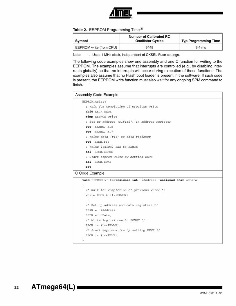
Note: 1. Uses 1 MHz clock, independent of CKSEL Fuse settings.
The following code examples show one assembly and one C function for writing to theEEPROM. The examples assume that interrupts are controlled (e.g., by disabling inter-rupts globally) so that no interrupts will occur during execution of these functions. Theexamples also assume that no Flash boot loader is present in the software. If such codeis present, the EEPROM write function must also wait for any ongoing SPM command tofinish.
Table 2. EEPROM Programming Time(1)
SymbolNumber of Calibrated RC
Oscillator Cycles Typ Programming Time
EEPROM write (from CPU) 8448 8.4 ms
Assembly Code Example
EEPROM_write:
; Wait for completion of previous write
sbic EECR,EEWE
rjmp EEPROM_write
; Set up address (r18:r17) in address register
out EEARH, r18
out EEARL, r17
; Write data (r16) to data register
out EEDR,r16
; Write logical one to EEMWE
sbi EECR,EEMWE
; Start eeprom write by setting EEWE
sbi EECR,EEWE
ret
C Code Example
void EEPROM_write(unsigned int uiAddress, unsigned char ucData)
/* Wait for completion of previous write */
while(EECR & (1<<EEWE))
;
/* Set up address and data registers */
EEAR = uiAddress;
EEDR = ucData;
/* Write logical one to EEMWE */
EECR |= (1<<EEMWE);
/* Start eeprom write by setting EEWE */
EECR |= (1<<EEWE);
22 ATmega64(L)2490I–AVR–11/04
ATmega64(L)
The next code examples show assembly and C functions for reading the EEPROM. Theexamples assume that interrupts are controlled so that no interrupts will occur duringexecution of these functions.
EEPROM Write During Power-down Sleep Mode
When entering Power-down Sleep mode while an EEPROM write operation is active,the EEPROM write operation will continue, and will complete before the Write Accesstime has passed. However, when the write operation is completed, the oscillator contin-ues running, and as a consequence, the device does not enter Power-down entirely. It istherefore recommended to verify that the EEPROM write operation is completed beforeentering Power-down.
Assembly Code Example
EEPROM_read:
; Wait for completion of previous write
sbic EECR,EEWE
rjmp EEPROM_read
; Set up address (r18:r17) in address register
out EEARH, r18
out EEARL, r17
; Start eeprom read by writing EERE
sbi EECR,EERE
; Read data from data register
in r16,EEDR
ret
C Code Example
unsigned char EEPROM_read(unsigned int uiAddress)
/* Wait for completion of previous write */
while(EECR & (1<<EEWE))
;
/* Set up address register */
EEAR = uiAddress;
/* Start eeprom read by writing EERE */
EECR |= (1<<EERE);
/* Return data from data register */
return EEDR;
232490I–AVR–11/04
Preventing EEPROM Corruption
During periods of low VCC, the EEPROM data can be corrupted because the supply volt-age is too low for the CPU and the EEPROM to operate properly. These issues are thesame as for board level systems using EEPROM, and the same design solutions shouldbe applied.
An EEPROM data corruption can be caused by two situations when the voltage is toolow. First, a regular write sequence to the EEPROM requires a minimum voltage tooperate correctly. Secondly, the CPU itself can execute instructions incorrectly, if thesupply voltage is too low.
EEPROM data corrupt ion can easi ly be avoided by fo l lowing th is designrecommendation:
Keep the AVR RESET active (low) during periods of insufficient power supply volt-age. This can be done by enabling the internal Brown-out Detector (BOD). If thedetection level of the internal BOD does not match the needed detection level, anexternal low VCC Reset Protection circuit can be used. If a reset occurs while a writeoperation is in progress, the write operation will be completed provided that thepower supply voltage is sufficient.
I/O Memory The I/O space definition of the ATmega64 is shown in “Register Summary” on page 372.
All ATmega64 I/Os and peripherals are placed in the I/O space. All I/O locations may beaccessed by the LD/LDS/LDD and ST/STS/STD instructions, transferring data betweenthe 32 general purpose working registers and the I/O space. I/O Registers within theaddress range 0x00 - 0x1F are directly bit-accessible using the SBI and CBI instruc-tions. In these registers, the value of single bits can be checked by using the SBIS andSBIC instructions. Refer to the instruction set section for more details. When using theI/O specific commands IN and OUT, the I/O addresses 0x00 - 0x3F must be used.When addressing I/O Registers as data space using LD and ST instructions, 0x20 mustbe added to these addresses. The ATmega64 is a complex microcontroller with moreperipheral units than can be supported within the 64 location reserved in Opcode for theIN and OUT instructions. For the Extended I/O space from 0x60 - 0xFF in SRAM, onlythe ST/STS/STD and LD/LDS/LDD instructions can be used. The Extended I/O space isreplaced with SRAM locations when the ATmega64 is in the ATmega103 compatibilitymode.
For compatibility with future devices, reserved bits should be written to zero if accessed.Reserved I/O memory addresses should never be written.
Some of the status flags are cleared by writing a logical one to them. Note that the CBIand SBI instructions will operate on all bits in the I/O Register, writing a one back intoany flag read as set, thus clearing the flag. The CBI and SBI instructions work with reg-isters 0x00 to 0x1F only.
The I/O and peripherals control registers are explained in later sections.
24 ATmega64(L)2490I–AVR–11/04
ATmega64(L)
External Memory Interface
With all the features that the External Memory Interface provides, it is well suited tooperate as an interface to memory devices such as external SRAM and Flash, andperipherals such as LCD-display, A/D, and D/A. The main features are:
• Four different wait-state settings (Including no wait-state).
• Independent wait-state setting for different external memory sectors (configurable sector size).
• The number of bits dedicated to address high byte is selectable.
• Bus Keepers on data lines to minimize current consumption (optional).
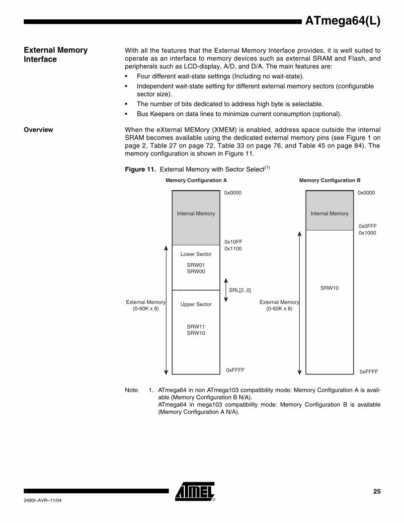
Overview When the eXternal MEMory (XMEM) is enabled, address space outside the internalSRAM becomes available using the dedicated external memory pins (see Figure 1 onpage 2, Table 27 on page 72, Table 33 on page 76, and Table 45 on page 84). Thememory configuration is shown in Figure 11.
Figure 11. External Memory with Sector Select(1)
Note: 1. ATmega64 in non ATmega103 compatibility mode: Memory Configuration A is avail-able (Memory Configuration B N/A).ATmega64 in mega103 compatibility mode: Memory Configuration B is available(Memory Configuration A N/A).
Memory Configuration A
0x0000
0x10FF
External Memory(0-60K x 8)
0xFFFF
Internal Memory
SRL[2..0]
SRW11SRW10
SRW01SRW00
Lower Sector
Upper Sector
0x1100
Memory Configuration B
0x0000
External Memory(0-60K x 8)
0xFFFF
Internal Memory
SRW10
0x0FFF0x1000
252490I–AVR–11/04
ATmega103 Compatibility Both External Memory Control Registers, XMCRA and XMCRB, are placed in ExtendedI/O space. In ATmega103 compatibility mode, these registers are not available, and thefeatures selected by these registers are not available. The device is still ATmega103compatible, as these features did not exist in ATmega103. The limitations inATmega103 compatibility mode are:
• Only two wait-state settings are available (SRW1n = 0b00 and SRW1n = 0b01).
• The number of bits that are assigned to address high byte are fixed.
• The external memory section cannot be divided into sectors with different wait-state settings.
• Bus Keeper is not available.
• RD, WR, and ALE pins are output only (Port G in ATmega64).
Using the External Memory Interface
The interface consists of:
• AD7:0: Multiplexed low-order address bus and data bus.
• A15:8: High-order address bus (configurable number of bits).
• ALE: Address latch enable.
• RD: Read strobe.
• WR: Write strobe.
The control bits for the External Memory Interface are located in three registers, theMCU Control Register – MCUCR, the External Memory Control Register A – XMCRA,and the External Memory Control Register B – XMCRB.
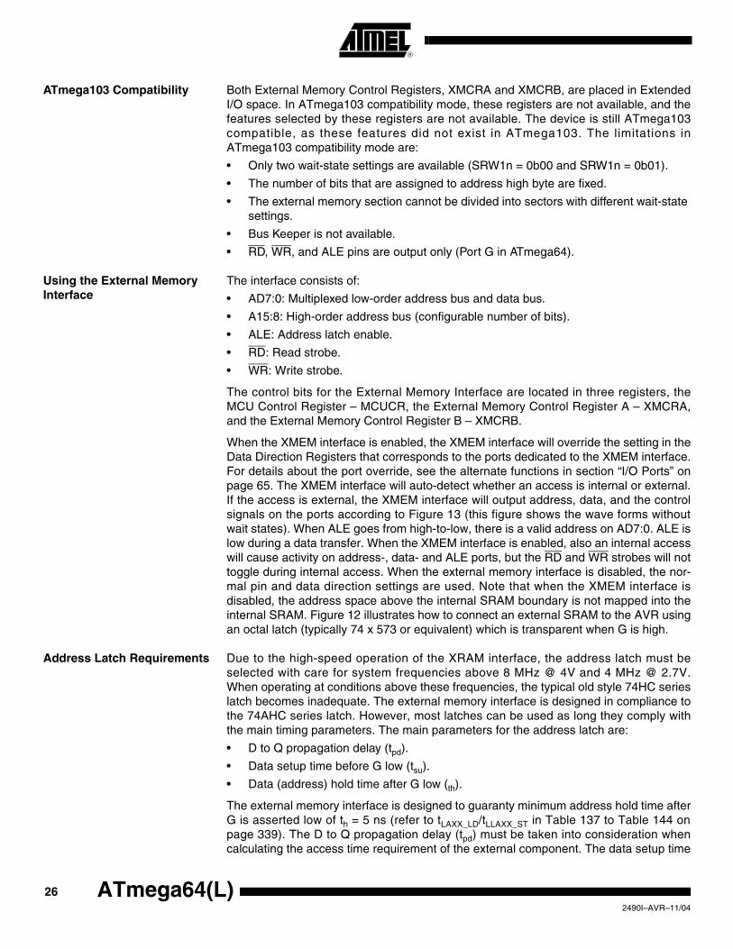
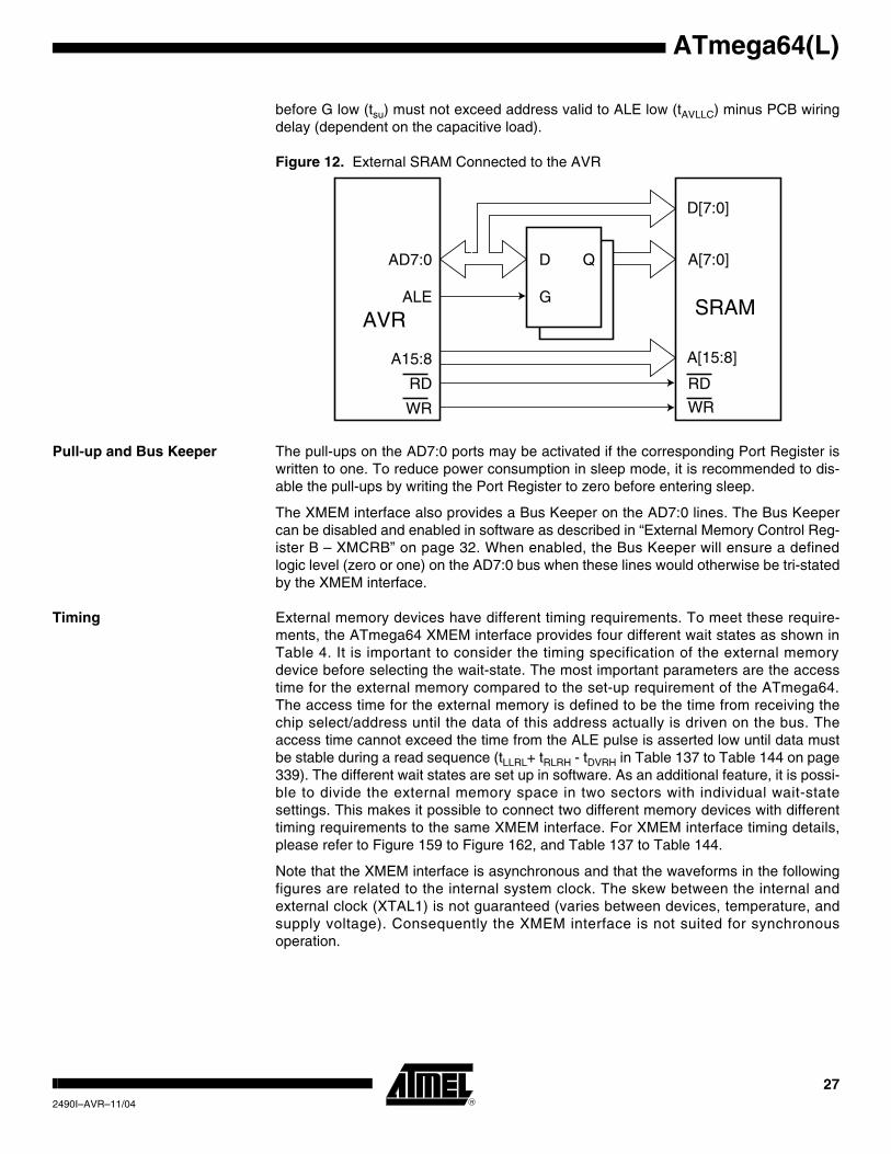
When the XMEM interface is enabled, the XMEM interface will override the setting in theData Direction Registers that corresponds to the ports dedicated to the XMEM interface.For details about the port override, see the alternate functions in section “I/O Ports” onpage 65. The XMEM interface will auto-detect whether an access is internal or external.If the access is external, the XMEM interface will output address, data, and the controlsignals on the ports according to Figure 13 (this figure shows the wave forms withoutwait states). When ALE goes from high-to-low, there is a valid address on AD7:0. ALE islow during a data transfer. When the XMEM interface is enabled, also an internal accesswill cause activity on address-, data- and ALE ports, but the RD and WR strobes will nottoggle during internal access. When the external memory interface is disabled, the nor-mal pin and data direction settings are used. Note that when the XMEM interface isdisabled, the address space above the internal SRAM boundary is not mapped into theinternal SRAM. Figure 12 illustrates how to connect an external SRAM to the AVR usingan octal latch (typically 74 x 573 or equivalent) which is transparent when G is high.
Address Latch Requirements Due to the high-speed operation of the XRAM interface, the address latch must beselected with care for system frequencies above 8 MHz @ 4V and 4 MHz @ 2.7V.When operating at conditions above these frequencies, the typical old style 74HC serieslatch becomes inadequate. The external memory interface is designed in compliance tothe 74AHC series latch. However, most latches can be used as long they comply withthe main timing parameters. The main parameters for the address latch are:
• D to Q propagation delay (tpd).
• Data setup time before G low (tsu).
• Data (address) hold time after G low (th).
The external memory interface is designed to guaranty minimum address hold time afterG is asserted low of th = 5 ns (refer to tLAXX_LD/tLLAXX_ST in Table 137 to Table 144 onpage 339). The D to Q propagation delay (tpd) must be taken into consideration whencalculating the access time requirement of the external component. The data setup time
26 ATmega64(L)2490I–AVR–11/04
ATmega64(L)
before G low (tsu) must not exceed address valid to ALE low (tAVLLC) minus PCB wiringdelay (dependent on the capacitive load).
Figure 12. External SRAM Connected to the AVR
Pull-up and Bus Keeper The pull-ups on the AD7:0 ports may be activated if the corresponding Port Register iswritten to one. To reduce power consumption in sleep mode, it is recommended to dis-able the pull-ups by writing the Port Register to zero before entering sleep.
The XMEM interface also provides a Bus Keeper on the AD7:0 lines. The Bus Keepercan be disabled and enabled in software as described in “External Memory Control Reg-ister B – XMCRB” on page 32. When enabled, the Bus Keeper will ensure a definedlogic level (zero or one) on the AD7:0 bus when these lines would otherwise be tri-statedby the XMEM interface.
Timing External memory devices have different timing requirements. To meet these require-ments, the ATmega64 XMEM interface provides four different wait states as shown inTable 4. It is important to consider the timing specification of the external memorydevice before selecting the wait-state. The most important parameters are the accesstime for the external memory compared to the set-up requirement of the ATmega64.The access time for the external memory is defined to be the time from receiving thechip select/address until the data of this address actually is driven on the bus. Theaccess time cannot exceed the time from the ALE pulse is asserted low until data mustbe stable during a read sequence (tLLRL+ tRLRH - tDVRH in Table 137 to Table 144 on page339). The different wait states are set up in software. As an additional feature, it is possi-ble to divide the external memory space in two sectors with individual wait-statesettings. This makes it possible to connect two different memory devices with differenttiming requirements to the same XMEM interface. For XMEM interface timing details,please refer to Figure 159 to Figure 162, and Table 137 to Table 144.
Note that the XMEM interface is asynchronous and that the waveforms in the followingfigures are related to the internal system clock. The skew between the internal andexternal clock (XTAL1) is not guaranteed (varies between devices, temperature, andsupply voltage). Consequently the XMEM interface is not suited for synchronousoperation.
D[7:0]
A[7:0]
A[15:8]
RD
WR
SRAM
D Q
G
AD7:0
ALE
A15:8
RD
WR
AVR
272490I–AVR–11/04
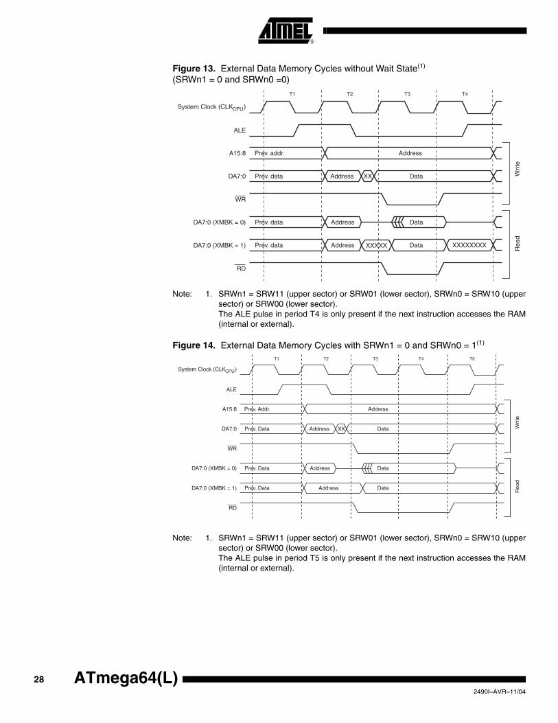
Figure 13. External Data Memory Cycles without Wait State(1) (SRWn1 = 0 and SRWn0 =0)
Note: 1. SRWn1 = SRW11 (upper sector) or SRW01 (lower sector), SRWn0 = SRW10 (uppersector) or SRW00 (lower sector).The ALE pulse in period T4 is only present if the next instruction accesses the RAM(internal or external).
Figure 14. External Data Memory Cycles with SRWn1 = 0 and SRWn0 = 1(1)
Note: 1. SRWn1 = SRW11 (upper sector) or SRW01 (lower sector), SRWn0 = SRW10 (uppersector) or SRW00 (lower sector).The ALE pulse in period T5 is only present if the next instruction accesses the RAM(internal or external).
ALE
T1 T2 T3
Writ
eR
ead
WR
T4
A15:8 AddressPrev. addr.
DA7:0 Address DataPrev. data XX
RD
DA7:0 (XMBK = 0) DataPrev. data Address
DataPrev. data AddressDA7:0 (XMBK = 1)
System Clock (CLKCPU)
XXXXX XXXXXXXX
ALE
T1 T2 T3
Writ
eR
ead
WR
T5
A15:8 AddressPrev. Addr.
DA7:0 Address DataPrev. Data XX
RD
DA7:0 (XMBK = 0) DataPrev. Data Address
DataPrev. Data AddressDA7:0 (XMBK = 1)
System Clock (CLKCPU)
T4
28 ATmega64(L)2490I–AVR–11/04
ATmega64(L)
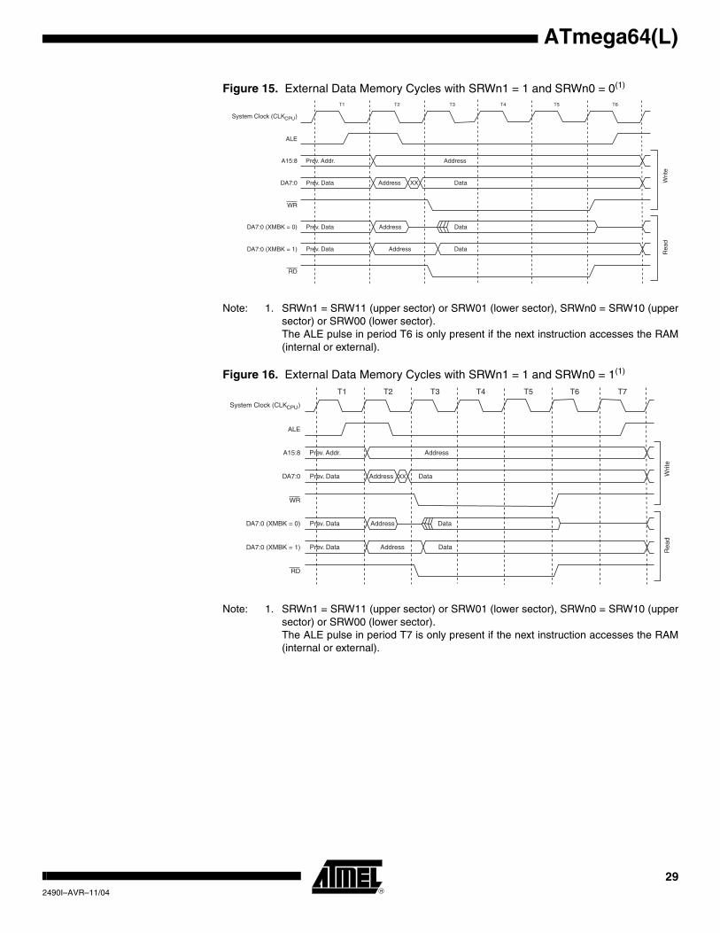
Figure 15. External Data Memory Cycles with SRWn1 = 1 and SRWn0 = 0(1)
Note: 1. SRWn1 = SRW11 (upper sector) or SRW01 (lower sector), SRWn0 = SRW10 (uppersector) or SRW00 (lower sector).The ALE pulse in period T6 is only present if the next instruction accesses the RAM(internal or external).
Figure 16. External Data Memory Cycles with SRWn1 = 1 and SRWn0 = 1(1)
Note: 1. SRWn1 = SRW11 (upper sector) or SRW01 (lower sector), SRWn0 = SRW10 (uppersector) or SRW00 (lower sector).The ALE pulse in period T7 is only present if the next instruction accesses the RAM(internal or external).
ALE
T1 T2 T3
Writ
eR
ead
WR
T6
A15:8 AddressPrev. Addr.
DA7:0 Address DataPrev. Data XX
RD
DA7:0 (XMBK = 0) DataPrev. Data Address
DataPrev. Data AddressDA7:0 (XMBK = 1)
System Clock (CLKCPU)
T4 T5
ALE
T1 T2 T3
Writ
eR
ead
WR
T7
A15:8 AddressPrev. Addr.
DA7:0 Address DataPrev. Data XX
RD
DA7:0 (XMBK = 0) DataPrev. Data Address
DataPrev. Data AddressDA7:0 (XMBK = 1)
System Clock (CLKCPU)
T4 T5 T6
292490I–AVR–11/04
XMEM Register Description
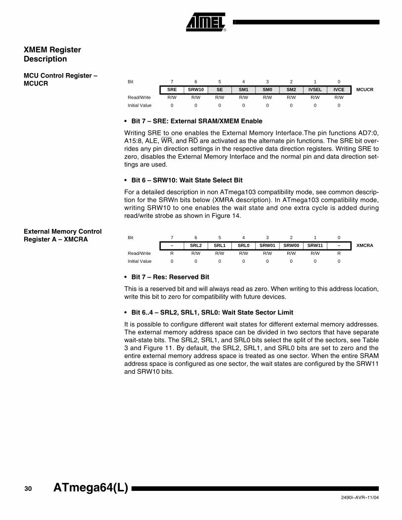
MCU Control Register – MCUCR
• Bit 7 – SRE: External SRAM/XMEM Enable
Writing SRE to one enables the External Memory Interface.The pin functions AD7:0,A15:8, ALE, WR, and RD are activated as the alternate pin functions. The SRE bit over-rides any pin direction settings in the respective data direction registers. Writing SRE tozero, disables the External Memory Interface and the normal pin and data direction set-tings are used.
• Bit 6 – SRW10: Wait State Select Bit
For a detailed description in non ATmega103 compatibility mode, see common descrip-tion for the SRWn bits below (XMRA description). In ATmega103 compatibility mode,writing SRW10 to one enables the wait state and one extra cycle is added duringread/write strobe as shown in Figure 14.
External Memory Control Register A – XMCRA
• Bit 7 – Res: Reserved Bit
This is a reserved bit and will always read as zero. When writing to this address location,write this bit to zero for compatibility with future devices.
• Bit 6..4 – SRL2, SRL1, SRL0: Wait State Sector Limit
It is possible to configure different wait states for different external memory addresses.The external memory address space can be divided in two sectors that have separatewait-state bits. The SRL2, SRL1, and SRL0 bits select the split of the sectors, see Table3 and Figure 11. By default, the SRL2, SRL1, and SRL0 bits are set to zero and theentire external memory address space is treated as one sector. When the entire SRAMaddress space is configured as one sector, the wait states are configured by the SRW11and SRW10 bits.
Bit 7 6 5 4 3 2 1 0
SRE SRW10 SE SM1 SM0 SM2 IVSEL IVCE MCUCRRead/Write R/W R/W R/W R/W R/W R/W R/W R/W
Initial Value 0 0 0 0 0 0 0 0
Bit 7 6 5 4 3 2 1 0
– SRL2 SRL1 SRL0 SRW01 SRW00 SRW11 – XMCRARead/Write R R/W R/W R/W R/W R/W R/W R
Initial Value 0 0 0 0 0 0 0 0
30 ATmega64(L)2490I–AVR–11/04
ATmega64(L)
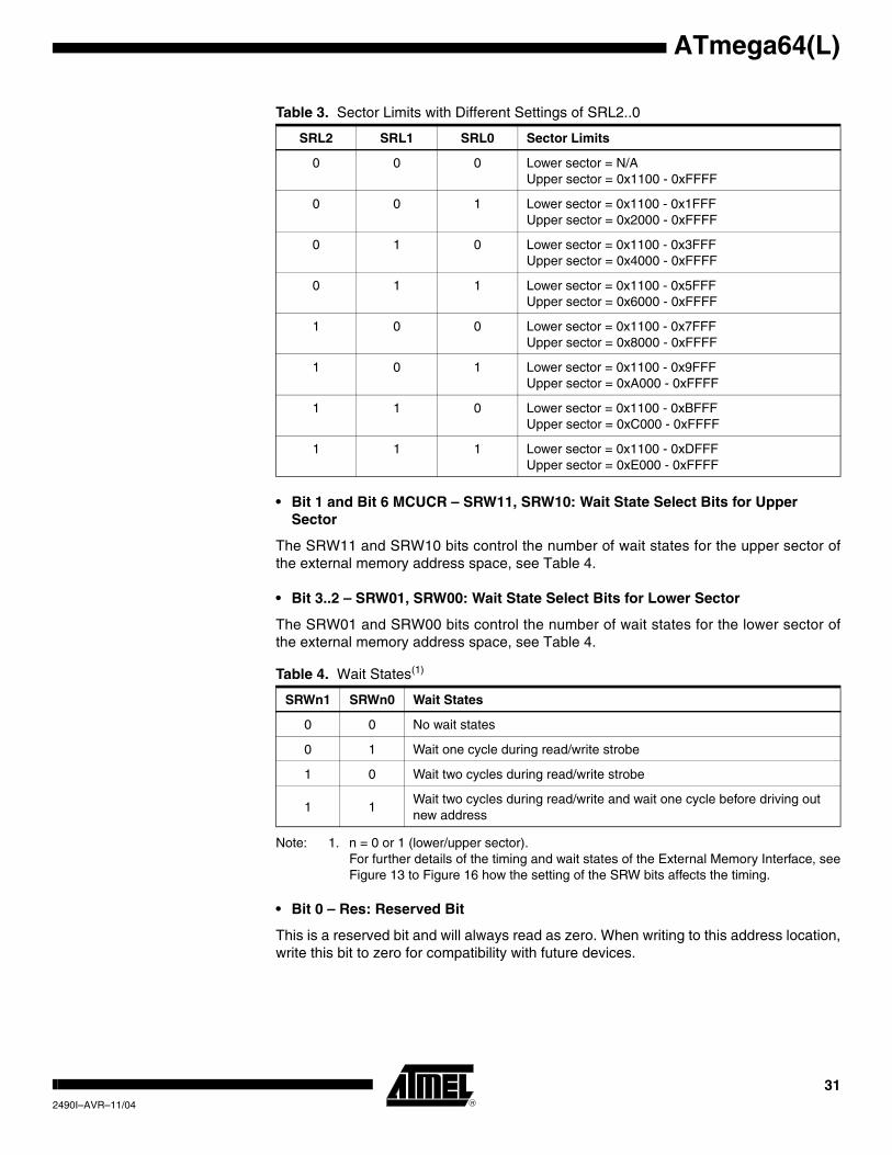
• Bit 1 and Bit 6 MCUCR – SRW11, SRW10: Wait State Select Bits for Upper Sector
The SRW11 and SRW10 bits control the number of wait states for the upper sector ofthe external memory address space, see Table 4.
• Bit 3..2 – SRW01, SRW00: Wait State Select Bits for Lower Sector
The SRW01 and SRW00 bits control the number of wait states for the lower sector ofthe external memory address space, see Table 4.
Note: 1. n = 0 or 1 (lower/upper sector).For further details of the timing and wait states of the External Memory Interface, seeFigure 13 to Figure 16 how the setting of the SRW bits affects the timing.
• Bit 0 – Res: Reserved Bit
This is a reserved bit and will always read as zero. When writing to this address location,write this bit to zero for compatibility with future devices.
Table 3. Sector Limits with Different Settings of SRL2..0
SRL2 SRL1 SRL0 Sector Limits
0 0 0 Lower sector = N/AUpper sector = 0x1100 - 0xFFFF
0 0 1 Lower sector = 0x1100 - 0x1FFFUpper sector = 0x2000 - 0xFFFF
0 1 0 Lower sector = 0x1100 - 0x3FFFUpper sector = 0x4000 - 0xFFFF
0 1 1 Lower sector = 0x1100 - 0x5FFFUpper sector = 0x6000 - 0xFFFF
1 0 0 Lower sector = 0x1100 - 0x7FFFUpper sector = 0x8000 - 0xFFFF
1 0 1 Lower sector = 0x1100 - 0x9FFFUpper sector = 0xA000 - 0xFFFF
1 1 0 Lower sector = 0x1100 - 0xBFFFUpper sector = 0xC000 - 0xFFFF
1 1 1 Lower sector = 0x1100 - 0xDFFFUpper sector = 0xE000 - 0xFFFF
Table 4. Wait States(1)
SRWn1 SRWn0 Wait States
0 0 No wait states
0 1 Wait one cycle during read/write strobe
1 0 Wait two cycles during read/write strobe
1 1Wait two cycles during read/write and wait one cycle before driving out new address
312490I–AVR–11/04
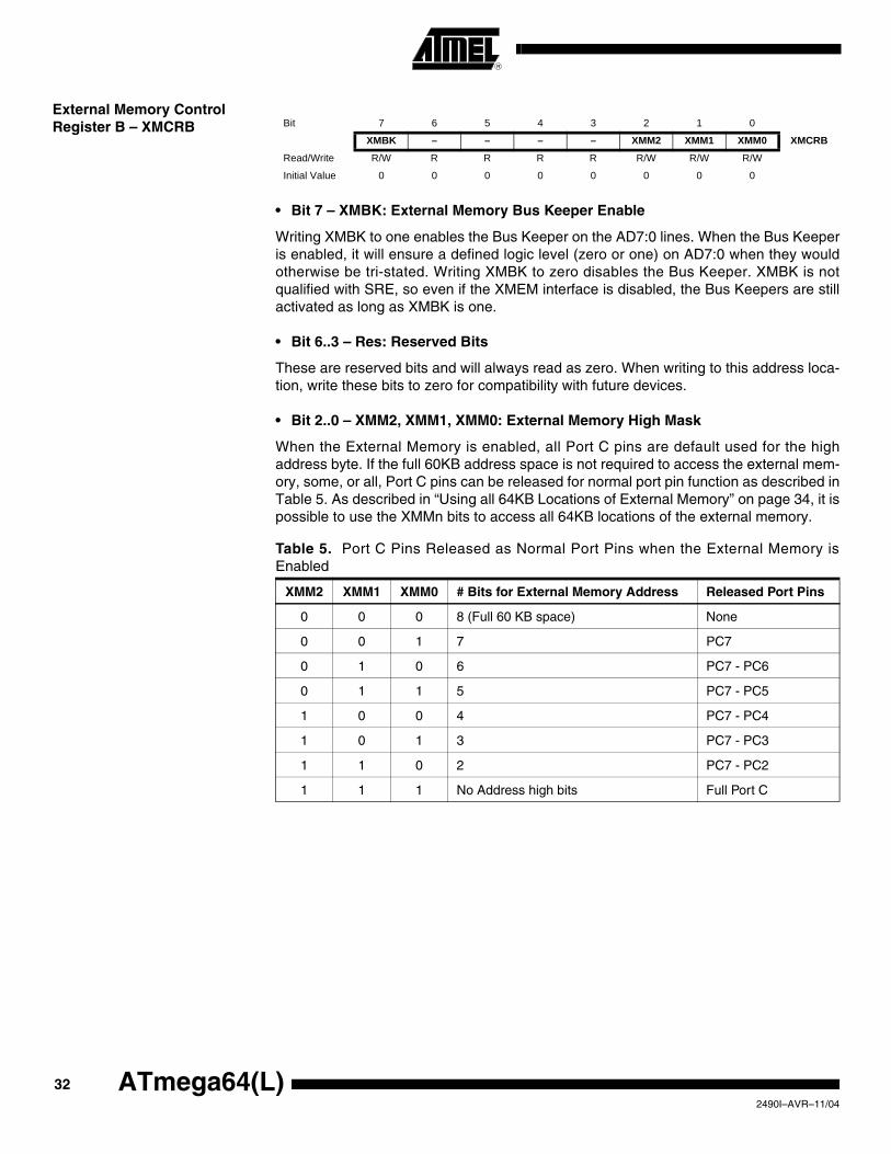
External Memory Control Register B – XMCRB
• Bit 7 – XMBK: External Memory Bus Keeper Enable
Writing XMBK to one enables the Bus Keeper on the AD7:0 lines. When the Bus Keeperis enabled, it will ensure a defined logic level (zero or one) on AD7:0 when they wouldotherwise be tri-stated. Writing XMBK to zero disables the Bus Keeper. XMBK is notqualified with SRE, so even if the XMEM interface is disabled, the Bus Keepers are stillactivated as long as XMBK is one.
• Bit 6..3 – Res: Reserved Bits
These are reserved bits and will always read as zero. When writing to this address loca-tion, write these bits to zero for compatibility with future devices.
• Bit 2..0 – XMM2, XMM1, XMM0: External Memory High Mask
When the External Memory is enabled, all Port C pins are default used for the highaddress byte. If the full 60KB address space is not required to access the external mem-ory, some, or all, Port C pins can be released for normal port pin function as described inTable 5. As described in “Using all 64KB Locations of External Memory” on page 34, it ispossible to use the XMMn bits to access all 64KB locations of the external memory.
Bit 7 6 5 4 3 2 1 0
XMBK – – – – XMM2 XMM1 XMM0 XMCRBRead/Write R/W R R R R R/W R/W R/W
Initial Value 0 0 0 0 0 0 0 0
Table 5. Port C Pins Released as Normal Port Pins when the External Memory isEnabled
XMM2 XMM1 XMM0 # Bits for External Memory Address Released Port Pins
0 0 0 8 (Full 60 KB space) None
0 0 1 7 PC7
0 1 0 6 PC7 - PC6
0 1 1 5 PC7 - PC5
1 0 0 4 PC7 - PC4
1 0 1 3 PC7 - PC3
1 1 0 2 PC7 - PC2
1 1 1 No Address high bits Full Port C
32 ATmega64(L)2490I–AVR–11/04
ATmega64(L)
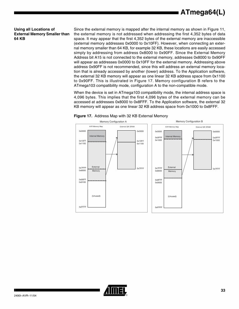
Using all Locations of External Memory Smaller than 64 KB
Since the external memory is mapped after the internal memory as shown in Figure 11,the external memory is not addressed when addressing the first 4,352 bytes of dataspace. It may appear that the first 4,352 bytes of the external memory are inaccessible(external memory addresses 0x0000 to 0x10FF). However, when connecting an exter-nal memory smaller than 64 KB, for example 32 KB, these locations are easily accessedsimply by addressing from address 0x8000 to 0x90FF. Since the External MemoryAddress bit A15 is not connected to the external memory, addresses 0x8000 to 0x90FFwill appear as addresses 0x0000 to 0x10FF for the external memory. Addressing aboveaddress 0x90FF is not recommended, since this will address an external memory loca-tion that is already accessed by another (lower) address. To the Application software,the external 32 KB memory will appear as one linear 32 KB address space from 0x1100to 0x90FF. This is illustrated in Figure 17. Memory configuration B refers to theATmega103 compatibility mode, configuration A to the non-compatible mode.
When the device is set in ATmega103 compatibility mode, the internal address space is4,096 bytes. This implies that the first 4,096 bytes of the external memory can beaccessed at addresses 0x8000 to 0x8FFF. To the Application software, the external 32KB memory will appear as one linear 32 KB address space from 0x1000 to 0x8FFF.
Figure 17. Address Map with 32 KB External Memory
0x0000
0x10FF
0xFFFF
0x1100
0x7FFF 0x8000
0x90FF 0x9100
0x0000
0x10FF 0x1100
0x7FFF
Memory Configuration A Memory Configuration B
Internal Memory
(Unused)
AVR Memory Map External 32K SRAM
External
Memory
0x0000
0x0FFF
0xFFFF
0x1000
0x7FFF 0x8000
0x8FFF 0x9000
0x0000
0x0FFF 0x1000
0x7FFF
Internal Memory
(Unused)
AVR Memory Map External 32K SRAM
External
Memory
332490I–AVR–11/04
Using all 64KB Locations of External Memory
Since the external memory is mapped after the internal memory as shown in Figure 11,only 60KB of external memory is available by default (address space 0x0000 to 0x10FFis reserved for internal memory). However, it is possible to take advantage of the entireexternal memory by masking the higher address bits to zero. This can be done by usingthe XMMn bits and controlled by software the most significant bits of the address. Bysetting Port C to output 0x00, and releasing the most significant bits for normal Port Pinoperation, the Memory Interface will address 0x0000 - 0x1FFF. See code examplesbelow.
Note: 1. The example code assumes that the part specific header file is included.
Care must be exercised using this option as most of the memory is masked away.
Assembly Code Example(1)
; OFFSET is defined to 0x2000 to ensure; external memory access; Configure Port C (address high byte) to; output 0x00 when the pins are released; for normal Port Pin operation
ldi r16, 0xFFout DDRC, r16ldi r16, 0x00out PORTC, r16; release PC7:5ldi r16, (1<<XMM1)|(1<<XMM0)sts XMCRB, r16; write 0xAA to address 0x0001 of external; memoryldi r16, 0xaasts 0x0001+OFFSET, r16; re-enable PC7:5 for external memoryldi r16, (0<<XMM1)|(0<<XMM0)sts XMCRB, r16; store 0x55 to address (OFFSET + 1) of; external memoryldi r16, 0x55sts 0x0001+OFFSET, r16
C Code Example(1)
#define OFFSET 0x2000
void XRAM_example(void)unsigned char *p = (unsigned char *) (OFFSET + 1);
DDRC = 0xFF;PORTC = 0x00;
XMCRB = (1<<XMM1) | (1<<XMM0);
*p = 0xaa;
XMCRB = 0x00;
*p = 0x55;
34 ATmega64(L)2490I–AVR–11/04
ATmega64(L)
System Clock and Clock Options
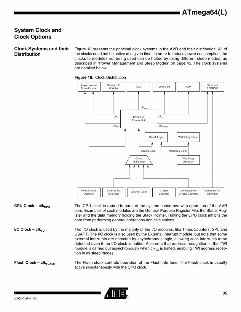
Clock Systems and their Distribution
Figure 18 presents the principal clock systems in the AVR and their distribution. All ofthe clocks need not be active at a given time. In order to reduce power consumption, theclocks to modules not being used can be halted by using different sleep modes, asdescribed in “Power Management and Sleep Modes” on page 45. The clock systemsare detailed below.
Figure 18. Clock Distribution
CPU Clock – clkCPU The CPU clock is routed to parts of the system concerned with operation of the AVRcore. Examples of such modules are the General Purpose Register File, the Status Reg-ister and the data memory holding the Stack Pointer. Halting the CPU clock inhibits thecore from performing general operations and calculations.
I/O Clock – clkI/O The I/O clock is used by the majority of the I/O modules, like Timer/Counters, SPI, andUSART. The I/O clock is also used by the External Interrupt module, but note that someexternal interrupts are detected by asynchronous logic, allowing such interrupts to bedetected even if the I/O clock is halted. Also note that address recognition in the TWImodule is carried out asynchronously when clkI/O is halted, enabling TWI address recep-tion in all sleep modes.
Flash Clock – clkFLASH The Flash clock controls operation of the Flash interface. The Flash clock is usuallyactive simultaneously with the CPU clock.
General I/OModules
AsynchronousTimer/Counter
ADC CPU Core RAM
clkI/O
clkASY
AVR ClockControl Unit
clkCPU
Flash andEEPROM
clkFLASH
clkADC
Source Clock
Watchdog Timer
WatchdogOscillator
Reset Logic
ClockMultiplexer
Watchdog Clock
Calibrated RCOscillator
Timer/CounterOscillator
CrystalOscillator
Low-frequencyCrystal Oscillator
External RCOscillator
External Clock
352490I–AVR–11/04
Asynchronous Timer Clock – clkASY
The Asynchronous Timer clock allows the Asynchronous Timer/Counter to be clockeddirectly from an external 32 kHz clock crystal. The dedicated clock domain allows usingthis Timer/Counter as a real-time counter even when the device is in sleep mode.
ADC Clock – clkADC The ADC is provided with a dedicated clock domain. This allows halting the CPU andI/O clocks in order to reduce noise generated by digital circuitry. This gives more accu-rate ADC conversion results.
Clock Sources The device has the following clock source options, selectable by Flash Fuse bits asshown below. The clock from the selected source is input to the AVR clock generator,and routed to the appropriate modules.
Note: 1. For all fuses “1” means unprogrammed while “0” means programmed.
The various choices for each clocking option is given in the following sections. When theCPU wakes up from Power-down or Power-save, the selected clock source is used totime the start-up, ensuring stable Oscillator operation before instruction execution starts.When the CPU starts from reset, there is as an additional delay allowing the power toreach a stable level before commencing normal operation. The Watchdog Oscillator isused for timing this real-time part of the start-up time. The number of WDT Oscillatorcycles used for each time-out is shown in Table 7. The frequency of the Watchdog Oscil-lator is voltage dependent as shown in the “ATmega64 Typical Characteristics” on page342.
Table 6. Device Clocking Options Select(1)
Device Clocking Option CKSEL3..0
External Crystal/Ceramic Resonator 1111 - 1010
External Low-frequency Crystal 1001
External RC Oscillator 1000 - 0101
Calibrated Internal RC Oscillator 0100 - 0001
External Clock 0000
Table 7. Number of Watchdog Oscillator Cycles
Typ Time-out (VCC = 5.0V) Typ Time-out (VCC = 3.0V) Number of Cycles
4.1 ms 4.3 ms 4K (4,096)
65 ms 69 ms 64K (65,536)
36 ATmega64(L)2490I–AVR–11/04
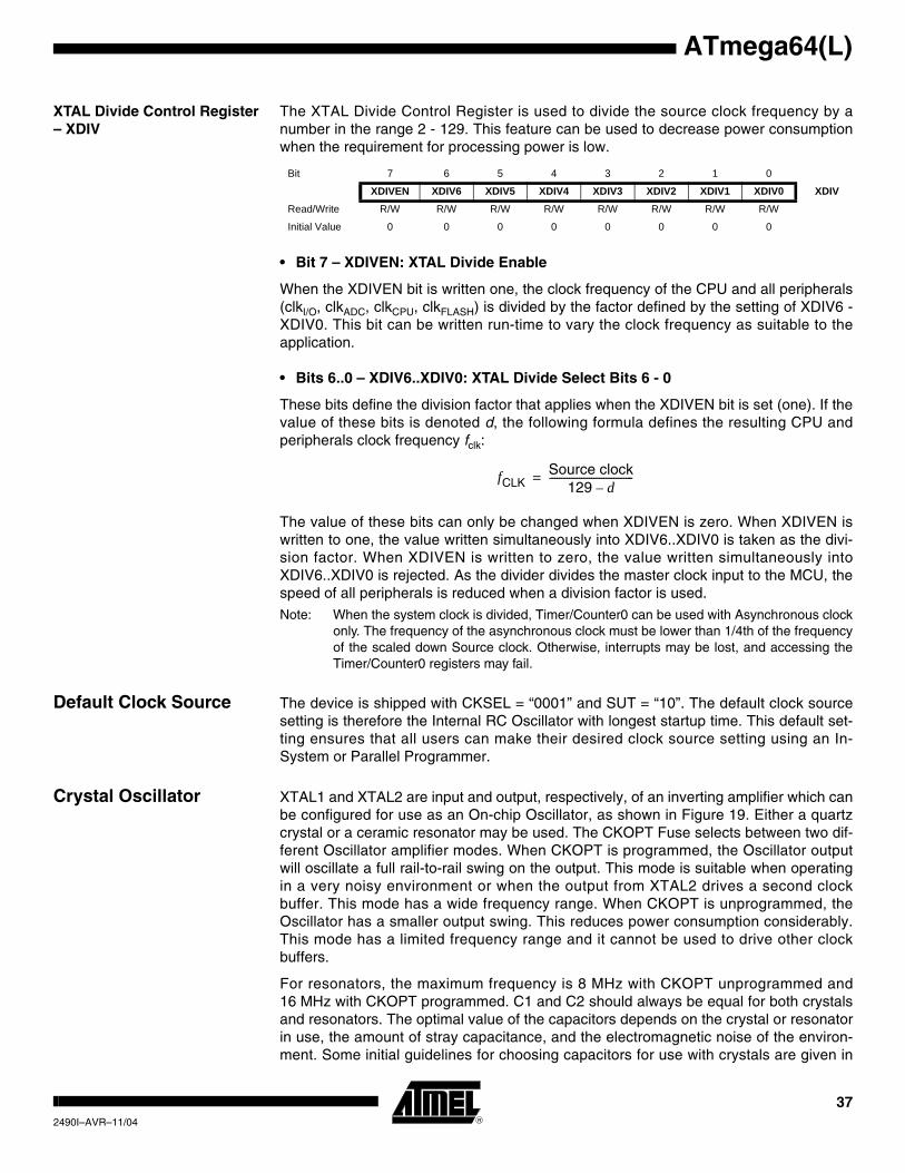
ATmega64(L)
XTAL Divide Control Register – XDIV
The XTAL Divide Control Register is used to divide the source clock frequency by anumber in the range 2 - 129. This feature can be used to decrease power consumptionwhen the requirement for processing power is low.
• Bit 7 – XDIVEN: XTAL Divide Enable
When the XDIVEN bit is written one, the clock frequency of the CPU and all peripherals(clkI/O, clkADC, clkCPU, clkFLASH) is divided by the factor defined by the setting of XDIV6 -XDIV0. This bit can be written run-time to vary the clock frequency as suitable to theapplication.
• Bits 6..0 – XDIV6..XDIV0: XTAL Divide Select Bits 6 - 0
These bits define the division factor that applies when the XDIVEN bit is set (one). If thevalue of these bits is denoted d, the following formula defines the resulting CPU andperipherals clock frequency fclk:
The value of these bits can only be changed when XDIVEN is zero. When XDIVEN iswritten to one, the value written simultaneously into XDIV6..XDIV0 is taken as the divi-sion factor. When XDIVEN is written to zero, the value written simultaneously intoXDIV6..XDIV0 is rejected. As the divider divides the master clock input to the MCU, thespeed of all peripherals is reduced when a division factor is used.Note: When the system clock is divided, Timer/Counter0 can be used with Asynchronous clock
only. The frequency of the asynchronous clock must be lower than 1/4th of the frequencyof the scaled down Source clock. Otherwise, interrupts may be lost, and accessing theTimer/Counter0 registers may fail.
Default Clock Source The device is shipped with CKSEL = “0001” and SUT = “10”. The default clock sourcesetting is therefore the Internal RC Oscillator with longest startup time. This default set-ting ensures that all users can make their desired clock source setting using an In-System or Parallel Programmer.
Crystal Oscillator XTAL1 and XTAL2 are input and output, respectively, of an inverting amplifier which canbe configured for use as an On-chip Oscillator, as shown in Figure 19. Either a quartzcrystal or a ceramic resonator may be used. The CKOPT Fuse selects between two dif-ferent Oscillator amplifier modes. When CKOPT is programmed, the Oscillator outputwill oscillate a full rail-to-rail swing on the output. This mode is suitable when operatingin a very noisy environment or when the output from XTAL2 drives a second clockbuffer. This mode has a wide frequency range. When CKOPT is unprogrammed, theOscillator has a smaller output swing. This reduces power consumption considerably.This mode has a limited frequency range and it cannot be used to drive other clockbuffers.
For resonators, the maximum frequency is 8 MHz with CKOPT unprogrammed and16 MHz with CKOPT programmed. C1 and C2 should always be equal for both crystalsand resonators. The optimal value of the capacitors depends on the crystal or resonatorin use, the amount of stray capacitance, and the electromagnetic noise of the environ-ment. Some initial guidelines for choosing capacitors for use with crystals are given in
Bit 7 6 5 4 3 2 1 0
XDIVEN XDIV6 XDIV5 XDIV4 XDIV3 XDIV2 XDIV1 XDIV0 XDIVRead/Write R/W R/W R/W R/W R/W R/W R/W R/W
Initial Value 0 0 0 0 0 0 0 0
fCLKSource clock
129 d–----------------------------------=
372490I–AVR–11/04
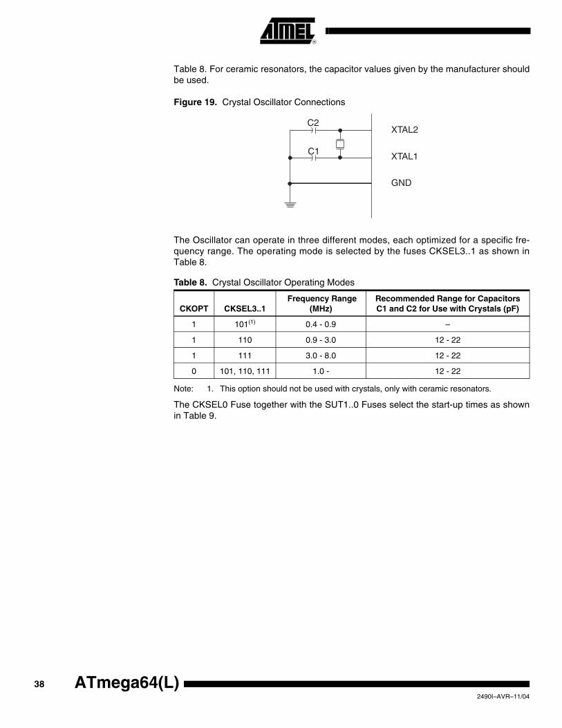
Table 8. For ceramic resonators, the capacitor values given by the manufacturer shouldbe used.
Figure 19. Crystal Oscillator Connections
The Oscillator can operate in three different modes, each optimized for a specific fre-quency range. The operating mode is selected by the fuses CKSEL3..1 as shown inTable 8.
Note: 1. This option should not be used with crystals, only with ceramic resonators.
The CKSEL0 Fuse together with the SUT1..0 Fuses select the start-up times as shownin Table 9.
Table 8. Crystal Oscillator Operating Modes
CKOPT CKSEL3..1 Frequency Range
(MHz)Recommended Range for Capacitors C1 and C2 for Use with Crystals (pF)
1 101(1) 0.4 - 0.9 –
1 110 0.9 - 3.0 12 - 22
1 111 3.0 - 8.0 12 - 22
0 101, 110, 111 1.0 - 12 - 22
XTAL2
XTAL1
GND
C2
C1
38 ATmega64(L)2490I–AVR–11/04
ATmega64(L)
Notes: 1. These options should only be used when not operating close to the maximum fre-quency of the device, and only if frequency stability at start-up is not important for theapplication. These options are not suitable for crystals.
2. These options are intended for use with ceramic resonators and will ensure fre-quency stability at start-up. They can also be used with crystals when not operatingclose to the maximum frequency of the device, and if frequency stability at start-up isnot important for the application.
Low-frequency Crystal Oscillator
To use a 32.768 kHz watch crystal as the clock source for the device, the Low-fre-quency crystal Oscillator must be selected by setting the CKSEL Fuses to “1001”. Thecrystal should be connected as shown in Figure 19. By programming the CKOPT Fuse,the user can enable internal capacitors on XTAL1 and XTAL2, thereby removing theneed for external capacitors. The internal capacitors have a nominal value of 36 pF.
When this Oscillator is selected, start-up times are determined by the SUT Fuses asshown in Table 10.
Note: 1. These options should only be used if frequency stability at start-up is not importantfor the application.
Table 9. Start-up Times for the Crystal Oscillator Clock Selection
CKSEL0 SUT1..0
Start-up Time from Power-down and
Power-save
Additional Delay from Reset(VCC = 5.0V) Recommended Usage
0 00 258 CK(1) 4.1 msCeramic resonator, fast rising power
0 01 258 CK(1) 65 msCeramic resonator, slowly rising power
0 10 1K CK(2) –Ceramic resonator, BOD enabled
0 11 1K CK(2) 4.1 msCeramic resonator, fast rising power
1 00 1K CK(2) 65 msCeramic resonator, slowly rising power
1 01 16K CK –Crystal Oscillator, BOD enabled
1 10 16K CK 4.1 msCrystal Oscillator, fast rising power
1 11 16K CK 65 msCrystal Oscillator, slowly rising power
Table 10. Start-up Times for the Low-frequency Crystal Oscillator Clock Selection
SUT1..0
Start-up Time from Power-down and Power-save
Additional Delay from Reset(VCC = 5.0V) Recommended Usage
00 1K CK(1) 4.1 ms Fast rising power or BOD enabled
01 1K CK(1) 65 ms Slowly rising power
10 32K CK 65 ms Stable frequency at start-up
11 Reserved
392490I–AVR–11/04
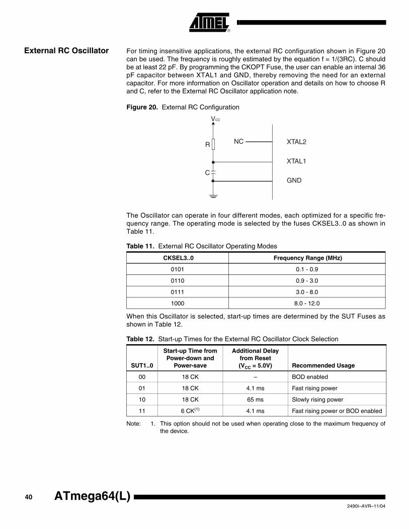
External RC Oscillator For timing insensitive applications, the external RC configuration shown in Figure 20can be used. The frequency is roughly estimated by the equation f = 1/(3RC). C shouldbe at least 22 pF. By programming the CKOPT Fuse, the user can enable an internal 36pF capacitor between XTAL1 and GND, thereby removing the need for an externalcapacitor. For more information on Oscillator operation and details on how to choose Rand C, refer to the External RC Oscillator application note.
Figure 20. External RC Configuration
The Oscillator can operate in four different modes, each optimized for a specific fre-quency range. The operating mode is selected by the fuses CKSEL3..0 as shown inTable 11.
When this Oscillator is selected, start-up times are determined by the SUT Fuses asshown in Table 12.
Note: 1. This option should not be used when operating close to the maximum frequency ofthe device.
Table 11. External RC Oscillator Operating Modes
CKSEL3..0 Frequency Range (MHz)
0101 0.1 - 0.9
0110 0.9 - 3.0
0111 3.0 - 8.0
1000 8.0 - 12.0
Table 12. Start-up Times for the External RC Oscillator Clock Selection
SUT1..0
Start-up Time from Power-down and
Power-save
Additional Delay from Reset (VCC = 5.0V) Recommended Usage
00 18 CK – BOD enabled
01 18 CK 4.1 ms Fast rising power
10 18 CK 65 ms Slowly rising power
11 6 CK(1) 4.1 ms Fast rising power or BOD enabled
XTAL2
XTAL1
GNDC
R
VCC
NC
40 ATmega64(L)2490I–AVR–11/04
ATmega64(L)
Calibrated Internal RC Oscillator
The calibrated internal RC Oscillator provides a fixed 1.0, 2.0, 4.0, or 8.0 MHz clock. Allfrequencies are nominal values at 5V and 25°C. This clock may be selected as the sys-tem clock by programming the CKSEL Fuses as shown in Table 13. If selected, it willoperate with no external components. The CKOPT Fuse should always be unpro-grammed when using this clock option. During reset, hardware loads the calibration byteinto the OSCCAL Register and thereby automatically calibrates the RC Oscillator. At 5V,25°C and 1.0 MHz Oscillator frequency selected, this calibration gives a frequencywithin ± 3% of the nominal frequency. Using run-time calibration methods as describedin application notes available at www.atmel.com/avr it is possible to achieve ± 1% accu-racy at any given VCC and Temperature. When this Oscillator is used as the chip clock,the Watchdog Oscillator will still be used for the Watchdog Timer and for the ResetTime-out. For more information on the preprogrammed calibration value, see the section“Calibration Byte” on page 294.
Note: 1. The device is shipped with this option selected.
When this Oscillator is selected, start-up times are determined by the SUT Fuses asshown in Table 14. XTAL1 and XTAL2 should be left unconnected (NC).
Note: 1. The device is shipped with this option selected.
Oscillator Calibration Register – OSCCAL(1)
Note: 1. The OSCCAL Register is not available in ATmega103 compatibility mode.
• Bits 7..0 – CAL7..0: Oscillator Calibration Value
Writing the calibration byte to this address will trim the internal Oscillator to remove pro-cess variations from the Oscillator frequency. During Reset, the 1 MHz calibration valuewhich is located in the signature row high byte (address 0x00) is automatically loadedinto the OSCCAL Register. If the internal RC is used at other frequencies, the calibrationvalues must be loaded manually. This can be done by first reading the signature row bya programmer, and then store the calibration values in the Flash or EEPROM. Then the
Table 13. Internal Calibrated RC Oscillator Operating Modes
CKSEL3..0 Nominal Frequency (MHz)
0001(1) 1.0
0010 2.0
0011 4.0
0100 8.0
Table 14. Start-up Times for the Internal Calibrated RC Oscillator Clock Selection
SUT1..0Start-up Time from Power-
down and Power-saveAdditional Delay from
Reset (VCC = 5.0V) Recommended Usage
00 6 CK – BOD enabled
01 6 CK 4.1 ms Fast rising power
10(1) 6 CK 65 ms Slowly rising power
11 Reserved
Bit 7 6 5 4 3 2 1 0
CAL7 CAL6 CAL5 CAL4 CAL3 CAL2 CAL1 CAL0 OSCCALRead/Write R/W R/W R/W R/W R/W R/W R/W R/W
Initial Value Device Specific Calibration Value
412490I–AVR–11/04
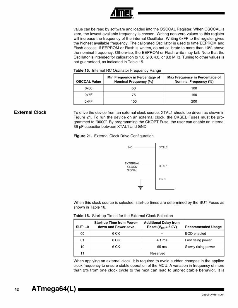
value can be read by software and loaded into the OSCCAL Register. When OSCCAL iszero, the lowest available frequency is chosen. Writing non-zero values to this registerwill increase the frequency of the internal Oscillator. Writing 0xFF to the register givesthe highest available frequency. The calibrated Oscillator is used to time EEPROM andFlash access. If EEPROM or Flash is written, do not calibrate to more than 10% abovethe nominal frequency. Otherwise, the EEPROM or Flash write may fail. Note that theOscillator is intended for calibration to 1.0, 2.0, 4.0, or 8.0 MHz. Tuning to other values isnot guaranteed, as indicated in Table 15.
External Clock To drive the device from an external clock source, XTAL1 should be driven as shown inFigure 21. To run the device on an external clock, the CKSEL Fuses must be pro-grammed to “0000”. By programming the CKOPT Fuse, the user can enable an internal36 pF capacitor between XTAL1 and GND.
Figure 21. External Clock Drive Configuration
When this clock source is selected, start-up times are determined by the SUT Fuses asshown in Table 16.
When applying an external clock, it is required to avoid sudden changes in the appliedclock frequency to ensure stable operation of the MCU. A variation in frequency of morethan 2% from one clock cycle to the next can lead to unpredictable behavior. It is
Table 15. Internal RC Oscillator Frequency Range
OSCCAL ValueMin Frequency in Percentage of
Nominal Frequency (%)Max Frequency in Percentage of
Nominal Frequency (%)
0x00 50 100
0x7F 75 150
0xFF 100 200
Table 16. Start-up Times for the External Clock Selection
SUT1..0Start-up Time from Power-
down and Power-saveAdditional Delay from
Reset (VCC = 5.0V) Recommended Usage
00 6 CK – BOD enabled
01 6 CK 4.1 ms Fast rising power
10 6 CK 65 ms Slowly rising power
11 Reserved
EXTERNALCLOCKSIGNAL
42 ATmega64(L)2490I–AVR–11/04

ATmega64(L)
required to ensure that the MCU is kept in Reset during such changes in the clockfrequency.
432490I–AVR–11/04

Timer/Counter Oscillator For AVR microcontrollers with Timer/Counter Oscillator pins (TOSC1 and TOSC2), thecrystal is connected directly between the pins. No external capacitors are needed. TheOscillator is optimized for use with a 32.768 kHz watch crystal. Applying an externalclock source to TOSC1 is not recommended.
44 ATmega64(L)2490I–AVR–11/04
ATmega64(L)
Power Management and Sleep Modes
Sleep modes enable the application to shut down unused modules in the MCU, therebysaving power. The AVR provides various sleep modes allowing the user to tailor thepower consumption to the application’s requirements.
To enter any of the six sleep modes, the SE-bit in MCUCR must be written to logic oneand a SLEEP instruction must be executed. The SM2, SM1, and SM0 bits in theMCUCR Register select which sleep mode (Idle, ADC Noise Reduction, Power-down,Power-save, Standby, or Extended Standby) will be activated by the SLEEP instruction.See Table 17 for a summary. If an enabled interrupt occurs while the MCU is in a sleepmode, the MCU wakes up. The MCU is then halted for four cycles in addition to thestart-up time, it executes the interrupt routine, and resumes execution from the instruc-tion following SLEEP. The contents of the Register File and SRAM are unaltered whenthe device wakes up from sleep. If a reset occurs during sleep mode, the MCU wakesup and executes from the Reset Vector.
Figure 18 on page 35 presents the different clock systems in the ATmega64, and theirdistribution. This figure is helpful in selecting an appropriate sleep mode.
MCU Control Register – MCUCR
The MCU Control Register contains control bits for power management.
• Bit 5 – SE: Sleep Enable
The SE bit must be written to logic one to make the MCU enter the sleep mode when theSLEEP instruction is executed. To avoid the MCU entering the sleep mode unless it isthe programmers purpose, it is recommended to write the Sleep Enable (SE) bit to onejust before the execution of the SLEEP instruction and to clear it immediately after wak-ing up.
• Bits 4..2 – SM2..0: Sleep Mode Select Bits 2, 1, and 0
These bits select between the six available sleep modes as shown in Table 17.
Note: 1. Standby mode and Extended Standby mode are only available with external crystalsor resonators.
Bit 7 6 5 4 3 2 1 0
SRE SRW10 SE SM1 SM0 SM2 IVSEL IVCE MCUCRRead/Write R/W R/W R/W R/W R/W R/W R/W R/W
Initial Value 0 0 0 0 0 0 0 0
Table 17. Sleep Mode Select
SM2 SM1 SM0 Sleep Mode
0 0 0 Idle
0 0 1 ADC Noise Reduction
0 1 0 Power-down
0 1 1 Power-save
1 0 0 Reserved
1 0 1 Reserved
1 1 0 Standby(1)
1 1 1 Extended Standby(1)
452490I–AVR–11/04
Idle Mode When the SM2..0 bits are written to 000, the SLEEP instruction makes the MCU enterIdle mode, stopping the CPU but allowing SPI, USART, Analog Comparator, ADC, Two-wire Serial Interface, Timer/Counters, Watchdog, and the interrupt system to continueoperating. This sleep mode basically halts clkCPU and clkFLASH, while allowing the otherclocks to run.
Idle mode enables the MCU to wake up from external triggered interrupts as well asinternal ones like the Timer Overflow and USART Transmit Complete interrupts. Ifwake-up from the Analog Comparator interrupt is not required, the Analog Comparatorcan be powered down by setting the ACD bit in the Analog Comparator Control and Sta-tus Register – ACSR. This will reduce power consumption in Idle mode. If the ADC isenabled, a conversion starts automatically when this mode is entered.
ADC Noise Reduction Mode
When the SM2..0 bits are written to 001, the SLEEP instruction makes the MCU enterADC Noise Reduction mode, stopping the CPU but allowing the ADC, the external inter-rupts, the Two-wire Serial Interface address watch, Timer/Counter0 and the Watchdogto continue operating (if enabled). This sleep mode basically halts clkI/O, clkCPU, andclk-FLASH, while allowing the other clocks to run.
This improves the noise environment for the ADC, enabling higher resolution measure-ments. If the ADC is enabled, a conversion starts automatically when this mode isentered. Apart form the ADC Conversion Complete interrupt, only an External Reset, aWatchdog Reset, a Brown-out Reset, a Two-wire Serial Interface address match inter-rupt, a Timer/Counter0 interrupt, an SPM/EEPROM ready interrupt, an external levelinterrupt on INT7:4, or an External Interrupt on INT3:0 can wake up the MCU from ADCNoise Reduction mode.
Power-down Mode When the SM2..0 bits are written to 010, the SLEEP instruction makes the MCU enterPower-down mode. In this mode, the external Oscillator is stopped, while the externalinterrupts, the Two-wire Serial Interface address watch, and the Watchdog continueoperating (if enabled). Only an External Reset, a Watchdog Reset, a Brown-out Reset, aTwo-wire Serial Interface address match interrupt, an external level interrupt on INT7:4,or an External Interrupt on INT3:0 can wake up the MCU. This sleep mode basicallyhalts all generated clocks, allowing operation of asynchronous modules only.
Note that if a level triggered interrupt is used for wake-up from Power-down mode, thechanged level must be held for some time to wake up the MCU. Refer to “External Inter-rupts” on page 89 for details.
When waking up from Power-down mode, there is a delay from the wake-up conditionoccurs until the wake-up becomes effective. This allows the clock to restart and becomestable after having been stopped. The wake-up period is defined by the same CKSELFuses that define the Reset Time-out period, as described in “Clock Sources” on page36.
Power-save Mode When the SM2..0 bits are written to 011, the SLEEP instruction makes the MCU enterPower-save mode. This mode is identical to Power-down, with one exception:
If Timer/Counter0 is clocked asynchronously (i.e., the AS0 bit in ASSR is set),Timer/Counter0 will run during sleep. The device can wake up from either Timer Over-f low or Output Compare event from Timer/Counter0 i f the correspondingTimer/Counter0 interrupt enable bits are set in TIMSK, and the Global Interrupt Enablebit in SREG is set.
If the asynchronous timer is NOT clocked asynchronously, Power-down mode is recom-mended instead of Power-save mode because the contents of the registers in the
46 ATmega64(L)2490I–AVR–11/04
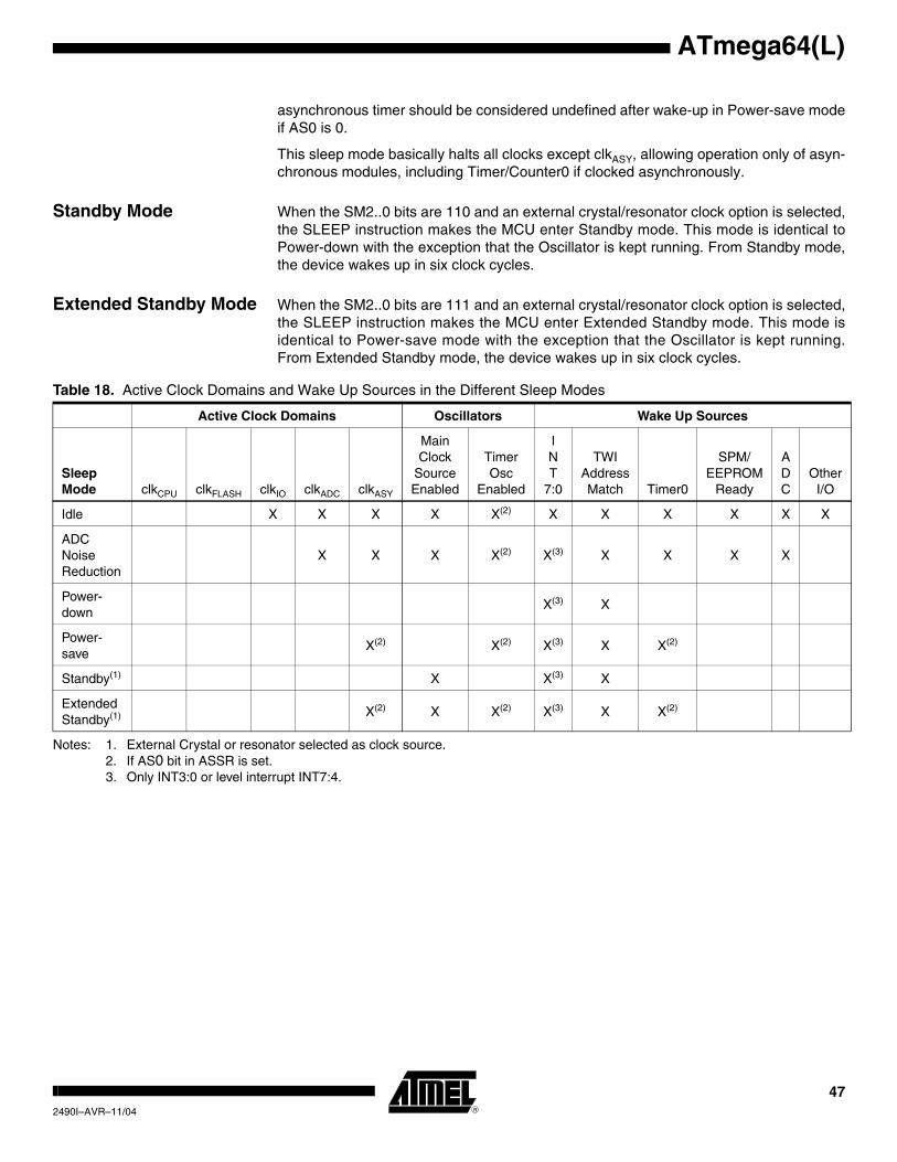
ATmega64(L)
asynchronous timer should be considered undefined after wake-up in Power-save modeif AS0 is 0.
This sleep mode basically halts all clocks except clkASY, allowing operation only of asyn-chronous modules, including Timer/Counter0 if clocked asynchronously.
Standby Mode When the SM2..0 bits are 110 and an external crystal/resonator clock option is selected,the SLEEP instruction makes the MCU enter Standby mode. This mode is identical toPower-down with the exception that the Oscillator is kept running. From Standby mode,the device wakes up in six clock cycles.
Extended Standby Mode When the SM2..0 bits are 111 and an external crystal/resonator clock option is selected,the SLEEP instruction makes the MCU enter Extended Standby mode. This mode isidentical to Power-save mode with the exception that the Oscillator is kept running.From Extended Standby mode, the device wakes up in six clock cycles.
Notes: 1. External Crystal or resonator selected as clock source.2. If AS0 bit in ASSR is set.3. Only INT3:0 or level interrupt INT7:4.
Table 18. Active Clock Domains and Wake Up Sources in the Different Sleep Modes
Active Clock Domains Oscillators Wake Up Sources
Sleep Mode clkCPU clkFLASH clkIO clkADC clkASY
MainClock
SourceEnabled
TimerOsc
Enabled
INT
7:0
TWIAddressMatch Timer0
SPM/EEPROM
Ready
ADC
OtherI/O
Idle X X X X X(2) X X X X X X
ADC NoiseReduction
X X X X(2) X(3) X X X X
Power-down
X(3) X
Power-save
X(2) X(2) X(3) X X(2)
Standby(1) X X(3) X
Extended Standby(1) X(2) X X(2) X(3) X X(2)
472490I–AVR–11/04
Minimizing Power Consumption
There are several issues to consider when trying to minimize the power consumption inan AVR controlled system. In general, sleep modes should be used as much as possi-ble, and the sleep mode should be selected so that as few as possible of the device’sfunctions are operating. All functions not needed should be disabled. In particular, thefollowing modules may need special consideration when trying to achieve the lowestpossible power consumption.
Analog to Digital Converter If enabled, the ADC will be enabled in all sleep modes. To save power, the ADC shouldbe disabled before entering any sleep mode. When the ADC is turned off and on again,the next conversion will be an extended conversion. Refer to “Analog to Digital Con-verter” on page 231 for details on ADC operation.
Analog Comparator When entering Idle mode, the Analog Comparator should be disabled if not used. Whenentering ADC Noise Reduction mode, the Analog Comparator should be disabled. In theother sleep modes, the Analog Comparator is automatically disabled. However, if theAnalog Comparator is set up to use the internal voltage reference as input, the AnalogComparator should be disabled in all sleep modes. Otherwise, the internal voltage refer-ence will be enabled, independent of sleep mode. Refer to “Analog Comparator” onpage 228 for details on how to configure the Analog Comparator.
Brown-out Detector If the Brown-out Detector is not needed in the application, this module should be turnedoff. If the Brown-out Detector is enabled by the BODEN Fuse, it will be enabled in allsleep modes, and hence, always consume power. In the deeper sleep modes, this willcontribute significantly to the total current consumption. Refer to “Brown-out Detector”on page 48 for details on how to configure the Brown-out Detector.
Internal Voltage Reference The internal voltage reference will be enabled when needed by the Brown-out Detector,the Analog Comparator or the ADC. If these modules are disabled as described in thesections above, the internal voltage reference will be disabled and it will not be consum-ing power. When turned on again, the user must allow the reference to start up beforethe output is used. If the reference is kept on in sleep mode, the output can be usedimmediately. Refer to “Internal Voltage Reference” on page 55 for details on the start-uptime.
Watchdog Timer If the Watchdog Timer is not needed in the application, this module should be turned off.If the Watchdog Timer is enabled, it will be enabled in all sleep modes, and hence,always consume power. In the deeper sleep modes, this will contribute significantly tothe total current consumption. Refer to “Watchdog Timer” on page 55 for details on howto configure the Watchdog Timer.
Port Pins When entering a sleep mode, all port pins should be configured to use minimum power.The most important thing is then to ensure that no pins drive resistive loads. In sleepmodes where the both the I/O clock (clkI/O) and the ADC clock (clkADC) are stopped, theinput buffers of the device will be disabled. This ensures that no power is consumed bythe input logic when not needed. In some cases, the input logic is needed for detectingwake-up conditions, and it will then be enabled. Refer to the section “Digital InputEnable and Sleep Modes” on page 69 for details on which pins are enabled. If the inputbuffer is enabled and the input signal is left floating or have an analog signal level closeto VCC/2, the input buffer will use excessive power.
48 ATmega64(L)2490I–AVR–11/04
ATmega64(L)
JTAG Interface and On-chip Debug System
If the On-chip debug system is enabled by the OCDEN Fuse and the chip enter Powerdown or Power save sleep mode, the main clock source remains enabled. In thesesleep modes, this will contribute significantly to the total current consumption. There arethree alternative ways to avoid this:
• Disable OCDEN Fuse.
• Disable JTAGEN Fuse.
• Write one to the JTD bit in MCUCSR.
The TDO pin is left floating when the JTAG interface is enabled while the JTAG TAPcontroller is not shifting data. If the hardware connected to the TDO pin does not pull upthe logic level, power consumption will increase. Note that the TDI pin for the nextdevice in the scan chain contains a pull-up that avoids this problem. Writing the JTD bitin the MCUCSR register to one or leaving the JTAG fuse unprogrammed disables theJTAG interface.
492490I–AVR–11/04
System Control and Reset
Resetting the AVR During Reset, all I/O Registers are set to their initial values, and the program starts exe-cution from the Reset Vector. The instruction placed at the Reset Vector must be a JMP– absolute jump – instruction to the Reset handling routine. If the program neverenables an interrupt source, the Interrupt Vectors are not used, and regular programcode can be placed at these locations. This is also the case if the Reset Vector is in theApplication section while the Interrupt Vectors are in the Boot section or vice versa. Thecircuit diagram in Figure 22 shows the Reset logic. Table 19 defines the electricalparameters of the Reset circuitry.
The I/O ports of the AVR are immediately Reset to their initial state when a reset sourcegoes active. This does not require any clock source to be running.
After all reset sources have gone inactive, a delay counter is invoked, stretching theInternal Reset. This allows the power to reach a stable level before normal operationstarts. The Time-out period of the delay counter is defined by the user through theCKSEL Fuses. The different selections for the delay period are presented in “ClockSources” on page 36.
Reset Sources The ATmega64 has five sources of reset:
• Power-on Reset. The MCU is reset when the supply voltage is below the Power-on Reset threshold (VPOT).
• External Reset. The MCU is reset when a low level is present on the RESET pin for longer than the minimum pulse length.
• Watchdog Reset. The MCU is reset when the Watchdog Timer period expires and the Watchdog is enabled.
• Brown-out Reset. The MCU is reset when the supply voltage VCC is below the Brown-out Reset threshold (VBOT) and the Brown-out Detector is enabled.
• JTAG AVR Reset. The MCU is reset as long as there is a logic one in the Reset Register, one of the scan chains of the JTAG system. Refer to the section “IEEE 1149.1 (JTAG) Boundary-scan” on page 255 for details.
50 ATmega64(L)2490I–AVR–11/04
ATmega64(L)
Figure 22. Reset Logic
Table 19. Reset Characteristics
Symbol Parameter Condition Min Typ Max Units
VPOT
Power-on Reset Threshold Voltage (rising)
1.4 2.3 V
Power-on Reset Threshold Voltage (falling)(1)
1.3 2.3 V
VRST RESET Pin Threshold Voltage
0.2 VCC 0.85 VCC V
tRSTMinimum pulse width on RESET Pin
1.5 µs
VBOT
Brown-out Reset Threshold Voltage(2)
BODLEVEL = 1 2.5 2.7 2.9V
BODLEVEL = 0 3.6 4.0 4.2
tBOD
Minimum low voltage period for Brown-out Detection
BODLEVEL = 1 2 µs
BODLEVEL = 0 2 µs
VHYSTBrown-out Detector hysteresis
120 mV
MCU Control and StatusRegister (MCUCSR)
Brown-OutReset Circuit
BODENBODLEVEL
Delay Counters
CKSEL[3:0]
CKTIMEOUT
WD
RF
BO
RF
EX
TR
F
PO
RF
DATA BUS
ClockGenerator
SPIKEFILTER
Pull-up Resistor
JTR
F
JTAG ResetRegister
WatchdogOscillator
SUT[1:0]
CO
UN
TE
R R
ES
ET
WatchdogTimer
RESET
Pull-up Resistor
PEN
Reset Circuit
L
D Q
Q
Power-On ResetCircuit
512490I–AVR–11/04
Notes: 1. The Power-on Reset will not work unless the supply voltage has been below VPOT(falling).
2. VBOT may be below nominal minimum operating voltage for some devices. Fordevices where this is the case, the device is tested down to VCC = VBOT during theproduction test. This guarantees that a Brown-out Reset will occur before VCC dropsto a voltage where correct operation of the microcontroller is no longer guaranteed.The test is performed using BODLEVEL=1 for ATmega64L and BODLEVEL=0 forATmega64. BODLEVEL=1 is not applicable for ATmega64.
Power-on Reset A Power-on Reset (POR) pulse is generated by an On-chip Detection circuit. The detec-tion level is defined in Table 19. The POR is activated whenever VCC is below thedetection level. The POR circuit can be used to trigger the Start-up Reset, as well as todetect a failure in supply voltage.
A Power-on Reset (POR) circuit ensures that the device is reset from Power-on. Reach-ing the Power-on Reset threshold voltage invokes the delay counter, which determineshow long the device is kept in RESET after VCC rise. The RESET signal is activatedagain, without any delay, when VCC decreases below the detection level.
Figure 23. MCU Start-up, RESET Tied to VCC
Figure 24. MCU Start-up, RESET Extended Externally
V
RESET
TIME-OUT
INTERNALRESET
tTOUT
VPOT
VRST
CC
RESET
TIME-OUT
INTERNALRESET
tTOUT
VPOT
VRST
VCC
52 ATmega64(L)2490I–AVR–11/04
ATmega64(L)
External Reset An External Reset is generated by a low level on the RESET pin. Reset pulses longerthan the minimum pulse width (see Table 19) will generate a reset, even if the clock isnot running. Shorter pulses are not guaranteed to generate a reset. When the appliedsignal reaches the Reset Threshold Voltage – VRST on its positive edge, the delaycounter starts the MCU after the Time-out period tTOUT has expired.
Figure 25. External Reset during Operation
Brown-out Detection ATmega64 has an On-chip Brown-out Detection (BOD) circuit for monitoring the VCClevel during operation by comparing it to a fixed trigger level. The trigger level for theBOD can be selected by the fuse BODLEVEL to be 2.7V (BODLEVEL unprogrammed),or 4.0V (BODLEVEL programmed). The trigger level has a hysteresis to ensure spikefree Brown-out Detection. The hysteresis on the detection level should be interpreted asVBOT+ = VBOT + VHYST/2 and VBOT- = VBOT - VHYST/2.
The BOD circuit can be enabled/disabled by the fuse BODEN. When the BOD isenabled (BODEN programmed), and VCC decreases to a value below the trigger level(VBOT- in Figure 26), the Brown-out Reset is immediately activated. When VCC increasesabove the trigger level (VBOT+ in Figure 26), the delay counter starts the MCU after theTime-out period tTOUT has expired.
The BOD circuit will only detect a drop in VCC if the voltage stays below the trigger levelfor longer than tBOD given in Table 19.
Figure 26. Borwn-out Reset During Operation
CC
VCC
RESET
TIME-OUT
INTERNALRESET
VBOT-VBOT+
tTOUT
532490I–AVR–11/04
Watchdog Reset When the Watchdog times out, it will generate a short reset pulse of one CK cycle dura-tion. On the falling edge of this pulse, the delay timer starts counting the Time-out periodtTOUT. Refer to page 55 for details on operation of the Watchdog Timer.
Figure 27. Watchdog Reset During Operation
MCU Control and Status Register – MCUCSR(1)
The MCU Control and Status Register provides information on which reset sourcecaused an MCU Reset.
Note: 1. Only EXTRF and PORF are available in mega103 compatibility mode.
• Bit 4 – JTRF: JTAG Reset Flag
This bit is set if a reset is being caused by a logic one in the JTAG Reset Registerselected by the JTAG instruction AVR_RESET. This bit is reset by a Brown-out Reset,or by writing a logic zero to the flag.
• Bit 3 – WDRF: Watchdog Reset Flag
This bit is set if a Watchdog Reset occurs. The bit is reset by a Power-on Reset, or bywriting a logic zero to the flag.
• Bit 2 – BORF: Brown-out Reset Flag
This bit is set if a Brown-out Reset occurs. The bit is reset by a Power-on Reset, or bywriting a logic zero to the flag.
• Bit 1 – EXTRF: External Reset Flag
This bit is set if an External Reset occurs. The bit is reset by a Power-on Reset, or bywriting a logic zero to the flag.
CK
CC
Bit 7 6 5 4 3 2 1 0
JTD – – JTRF WDRF BORF EXTRF PORF MCUCSRRead/Write R/W R R R/W R/W R/W R/W R/W
Initial Value 0 0 0 See Bit Description
54 ATmega64(L)2490I–AVR–11/04
ATmega64(L)
• Bit 0 – PORF: Power-on Reset Flag
This bit is set if a Power-on Reset occurs. The bit is reset only by writing a logic zero tothe flag.
To make use of the reset flags to identify a reset condition, the user should read andthen reset the MCUCSR as early as possible in the program. If the register is clearedbefore another reset occurs, the source of the reset can be found by examining theReset Flags.
Internal Voltage Reference
ATmega64 features an internal bandgap reference. This reference is used for Brown-out Detection, and it can be used as an input to the Analog Comparator or the ADC. The2.56V reference to the ADC is generated from the internal bandgap reference.
Voltage Reference Enable Signals and Start-up Time
The voltage reference has a start-up time that may influence the way it should be used.The start-up time is given in Table 20. To save power, the reference is not always turnedon. The reference is on during the following situations:
1. When the BOD is enabled (by programming the BODEN Fuse).
2. When the bandgap reference is connected to the Analog Comparator (by setting the ACBG bit in ACSR).
3. When the ADC is enabled.
Thus, when the BOD is not enabled, after setting the ACBG bit or enabling the ADC, theuser must always allow the reference to start up before the output from the Analog Com-parator or ADC is used. To reduce power consumption in Power-down mode, the usercan avoid the three conditions above to ensure that the reference is turned off beforeentering Power-down mode.
Watchdog Timer The Watchdog Timer is clocked from a separate On-chip Oscillator which runs at 1 Mhz.This is the typical value at VCC = 5V. See characterization data for typical values at otherVCC levels. By controlling the Watchdog Timer prescaler, the Watchdog Reset intervalcan be adjusted as shown in Table 22 on page 57. The WDR – Watchdog Reset –instruction resets the Watchdog Timer. The Watchdog Timer is also reset when it is dis-abled and when a Chip Reset occurs. Eight different clock cycle periods can be selectedto determine the reset period. If the reset period expires without another WatchdogReset, the ATmega64 resets and executes from the Reset Vector. For timing details onthe Watchdog Reset, refer to page 54.
To prevent unintentional disabling of the Watchdog or unintentional change of Time-outperiod, three different safety levels are selected by the fuses M103C and WDTON asshown in Table 21. Safety level 0 corresponds to the setting in ATmega103. There is norestriction on enabling the WDT in any of the safety levels. Refer to “Timed Sequencesfor Changing the Configuration of the Watchdog Timer” on page 59 for details.
Table 20. Internal Voltage Reference Characteristics
Symbol Parameter Min Typ Max Units
VBG Bandgap reference voltage 1.15 1.23 1.35 V
tBG Bandgap reference start-up time 40 70 µs
IBG Bandgap reference current consumption 10 µA
552490I–AVR–11/04
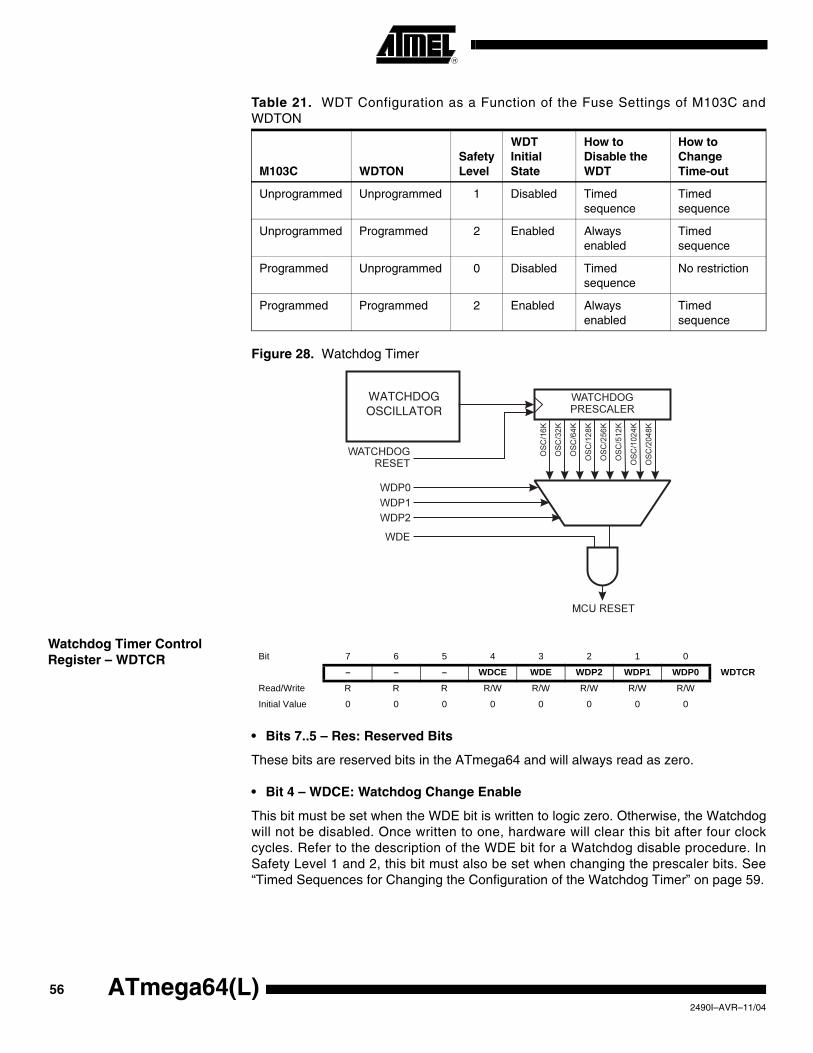
Figure 28. Watchdog Timer
Watchdog Timer Control Register – WDTCR
• Bits 7..5 – Res: Reserved Bits
These bits are reserved bits in the ATmega64 and will always read as zero.
• Bit 4 – WDCE: Watchdog Change Enable
This bit must be set when the WDE bit is written to logic zero. Otherwise, the Watchdogwill not be disabled. Once written to one, hardware will clear this bit after four clockcycles. Refer to the description of the WDE bit for a Watchdog disable procedure. InSafety Level 1 and 2, this bit must also be set when changing the prescaler bits. See“Timed Sequences for Changing the Configuration of the Watchdog Timer” on page 59.
Table 21. WDT Configuration as a Function of the Fuse Settings of M103C andWDTON
M103C WDTONSafety Level
WDT Initial State
How to Disable the WDT
How to Change Time-out
Unprogrammed Unprogrammed 1 Disabled Timed sequence
Timed sequence
Unprogrammed Programmed 2 Enabled Always enabled
Timed sequence
Programmed Unprogrammed 0 Disabled Timed sequence
No restriction
Programmed Programmed 2 Enabled Always enabled
Timed sequence
WATCHDOGOSCILLATOR
Bit 7 6 5 4 3 2 1 0
– – – WDCE WDE WDP2 WDP1 WDP0 WDTCRRead/Write R R R R/W R/W R/W R/W R/W
Initial Value 0 0 0 0 0 0 0 0
56 ATmega64(L)2490I–AVR–11/04
ATmega64(L)
• Bit 3 – WDE: Watchdog Enable
When the WDE is written to logic one, the Watchdog Timer is enabled, and if the WDE iswritten to logic zero, the Watchdog Timer function is disabled. WDE can only be clearedif the WDCE bit has logic level one. To disable an enabled Watchdog Timer, the follow-ing procedure must be followed:
1. In the same operation, write a logic one to WDCE and WDE. A logic one must be written to WDE even though it is set to one before the disable operation starts.
2. Within the next four clock cycles, write a logic 0 to WDE. This disables the Watchdog.
In safety level 2, it is not possible to disable the Watchdog Timer, even with the algo-rithm described above. See “Timed Sequences for Changing the Configuration of theWatchdog Timer” on page 59.
• Bits 2..0 – WDP2, WDP1, WDP0: Watchdog Timer Prescaler 2, 1, and 0
The WDP2, WDP1, and WDP0 bits determine the Watchdog Timer prescaling when theWatchdog Timer is enabled. The different prescaling values and their correspondingTimeout Periods are shown in Table 22.
Table 22. Watchdog Timer Prescale Select
WDP2 WDP1 WDP0Number of WDT Oscillator Cycles
Typical Time-out at VCC = 3.0V
Typical Time-out at VCC = 5.0V
0 0 0 16K (16,384) 17.1 ms 16.3 ms
0 0 1 32K (32,768) 34.3 ms 32.5 ms
0 1 0 64K (65,536) 68.5 ms 65 ms
0 1 1 128K (131,072) 0.14 s 0.13 s
1 0 0 256K (262,144) 0.27 s 0.26 s
1 0 1 512K (524,288) 0.55 s 0.52 s
1 1 0 1,024K (1,048,576) 1.1 s 1.0 s
1 1 1 2,048K (2,097,152) 2.2 s 2.1 s
572490I–AVR–11/04
The following code examples show one assembly and one C function for turning off theWDT. The examples assume that interrupts are controlled (e.g., by disabling interruptsglobally) so that no interrupts will occur during execution of these functions.
Assembly Code Example
WDT_off:
; reset WDT
wdr
in r16, WDTCR
ldi r16, (1<<WDCE)|(1<<WDE)
; Write logical one to WDCE and WDE
ori r16, (1<<WDCE)|(1<<WDE)
out WDTCR, r16
; Turn off WDT
ldi r16, (0<<WDE)
out WDTCR, r16
ret
C Code Example
void WDT_off(void)
/* Reset WDT*/
_WDRC();
/* Write logical one to WDCE and WDE */
WDTCR |= (1<<WDCE) | (1<<WDE);
/* Turn off WDT */
WDTCR = 0x00;
58 ATmega64(L)2490I–AVR–11/04
ATmega64(L)
Timed Sequences for Changing the Configuration of the Watchdog Timer
The sequence for changing configuration differs slightly between the three safety levels.Separate procedures are described for each level.
Safety Level 0 This mode is compatible with the Watchdog operation found in ATmega103. The Watch-dog Timer is initially disabled, but can be enabled by writing the WDE bit to 1 withoutany restriction. The Time-out period can be changed at any time without restriction. Todisable an enabled Watchdog Timer, the procedure described on page 57 (WDE bitdescription) must be followed.
Safety Level 1 In this mode, the Watchdog Timer is initially disabled, but can be enabled by writing theWDE bit to 1 without any restriction. A timed sequence is needed when changing theWatchdog Time-out period or disabling an enabled Watchdog Timer. To disable anenabled Watchdog Timer, and/or changing the Watchdog Time-out, the following proce-dure must be followed:
1. In the same operation, write a logic one to WDCE and WDE. A logic one must be written to WDE regardless of the previous value of the WDE bit.
2. Within the next four clock cycles, in the same operation, write the WDE and WDP bits as desired, but with the WDCE bit cleared.
Safety Level 2 In this mode, the Watchdog Timer is always enabled, and the WDE bit will always readas one. A timed sequence is needed when changing the Watchdog Time-out period. Tochange the Watchdog Time-out, the following procedure must be followed:
1. In the same operation, write a logical one to WDCE and WDE. Even though the WDE always is set, the WDE must be written to one to start the timed sequence.
2. Within the next four clock cycles, in the same operation, write the WDP bits as desired, but with the WDCE bit cleared. The value written to the WDE bit is irrelevant.
592490I–AVR–11/04
Interrupts This section describes the specifics of the interrupt handling as performed inATmega64. For a general explanation of the AVR interrupt handling, refer to “Reset andInterrupt Handling” on page 13.
Interrupt Vectors in ATmega64 Table 23. Reset and Interrupt Vectors
Vector No.
ProgramAddress(2) Source Interrupt Definition
1 0x0000(1) RESET External Pin, Power-on Reset, Brown-out Reset, Watchdog Reset, and JTAG AVR Reset
2 0x0002 INT0 External Interrupt Request 0
3 0x0004 INT1 External Interrupt Request 1
4 0x0006 INT2 External Interrupt Request 2
5 0x0008 INT3 External Interrupt Request 3
6 0x000A INT4 External Interrupt Request 4
7 0x000C INT5 External Interrupt Request 5
8 0x000E INT6 External Interrupt Request 6
9 0x0010 INT7 External Interrupt Request 7
10 0x0012 TIMER2 COMP Timer/Counter2 Compare Match
11 0x0014 TIMER2 OVF Timer/Counter2 Overflow
12 0x0016 TIMER1 CAPT Timer/Counter1 Capture Event
13 0x0018 TIMER1 COMPA Timer/Counter1 Compare Match A
14 0x001A TIMER1 COMPB Timer/Counter1 Compare Match B
15 0x001C TIMER1 OVF Timer/Counter1 Overflow
16 0x001E TIMER0 COMP Timer/Counter0 Compare Match
17 0x0020 TIMER0 OVF Timer/Counter0 Overflow
18 0x0022 SPI, STC SPI Serial Transfer Complete
19 0x0024 USART0, RX USART0, Rx Complete
20 0x0026 USART0, UDRE USART0 Data Register Empty
21 0x0028 USART0, TX USART0, Tx Complete
22 0x002A ADC ADC Conversion Complete
23 0x002C EE READY EEPROM Ready
24 0x002E ANALOG COMP Analog Comparator
25 0x0030(3) TIMER1 COMPC Timer/Countre1 Compare Match C
26 0x0032(3) TIMER3 CAPT Timer/Counter3 Capture Event
27 0x0034(3) TIMER3 COMPA Timer/Counter3 Compare Match A
28 0x0036(3) TIMER3 COMPB Timer/Counter3 Compare Match B
29 0x0038(3) TIMER3 COMPC Timer/Counter3 Compare Match C
30 0x003A(3) TIMER3 OVF Timer/Counter3 Overflow
31 0x003C(3) USART1, RX USART1, Rx Complete
60 ATmega64(L)2490I–AVR–11/04
ATmega64(L)
Notes: 1. When the BOOTRST Fuse is programmed, the device will jump to the Boot Loaderaddress at reset, see “Boot Loader Support – Read-While-Write Self-programming”on page 278.
2. When the IVSEL bit in MCUCR is set, Interrupt Vectors will be moved to the start ofthe Boot Flash section. The address of each Interrupt Vector will then be address inthis table added to the start address of the Boot Flash section.
3. The Interrupts on address 0x0030 - 0x0044 do not exist in ATmega103 compatibilitymode.
Table 24 shows Reset and Interrupt Vectors placement for the various combinations ofBOOTRST and IVSEL settings. If the program never enables an interrupt source, theInterrupt Vectors are not used, and regular program code can be placed at these loca-tions. This is also the case if the Reset Vector is in the Application section while theInterrupt Vectors are in the Boot section or vice versa.
Note: 1. The Boot Reset Address is shown in Table 112 on page 290. For the BOOTRSTFuse “1” means unprogrammed while “0” means programmed.
The most typical and general program setup for the Reset and Interrupt VectorAddresses in ATmega64 is:
Address Labels Code Comments
0x0000 jmp RESET ; Reset Handler
0x0002 jmp EXT_INT0 ; IRQ0 Handler
0x0004 jmp EXT_INT1 ; IRQ1 Handler
0x0006 jmp EXT_INT2 ; IRQ2 Handler
0x0008 jmp EXT_INT3 ; IRQ3 Handler
0x000A jmp EXT_INT4 ; IRQ4 Handler
0x000C jmp EXT_INT5 ; IRQ5 Handler
0x000E jmp EXT_INT6 ; IRQ6 Handler
0x0010 jmp EXT_INT7 ; IRQ7 Handler
0x0012 jmp TIM2_COMP ; Timer2 Compare Handler
0x0014 jmp TIM2_OVF ; Timer2 Overflow Handler
0x0016 jmp TIM1_CAPT ; Timer1 Capture Handler
0x0018 jmp TIM1_COMPA ; Timer1 CompareA Handler
0x001A jmp TIM1_COMPB ; Timer1 CompareB Handler
0x001C jmp TIM1_OVF ; Timer1 Overflow Handler
32 0x003E(3) USART1, UDRE USART1 Data Register Empty
33 0x0040(3) USART1, TX USART1, Tx Complete
34 0x0042(3) TWI Two-wire Serial Interface
35 0x0044(3) SPM READY Store Program Memory Ready
Table 24. Reset and Interrupt Vectors Placement(1)
BOOTRST IVSEL Reset Address Interrupt Vectors Start Address
1 0 0x0000 0x0002
1 1 0x0000 Boot Reset Address + 0x0002
0 0 Boot Reset Address 0x0002
0 1 Boot Reset Address Boot Reset Address + 0x0002
Table 23. Reset and Interrupt Vectors (Continued)
Vector No.
ProgramAddress(2) Source Interrupt Definition
612490I–AVR–11/04
0x001E jmp TIM0_COMP ; Timer0 Compare Handler
0x0020 jmp TIM0_OVF ; Timer0 Overflow Handler
0x0022 jmp SPI_STC ; SPI Transfer Complete Handler
0x0024 jmp USART0_RXC ; USART0 RX Complete Handler
0x0026 jmp USART0_DRE ; USART0,UDR Empty Handler
0x0028 jmp USART0_TXC ; USART0 TX Complete Handler
0x002A jmp ADC ; ADC Conversion Complete Handler
0x002C jmp EE_RDY ; EEPROM Ready Handler
0x002E jmp ANA_COMP ; Analog Comparator Handler
0x0030 jmp TIM1_COMPC ; Timer1 CompareC Handler
0x0032 jmp TIM3_CAPT ; Timer3 Capture Handler
0x0034 jmp TIM3_COMPA ; Timer3 CompareA Handler
0x0036 jmp TIM3_COMPB ; Timer3 CompareB Handler
0x0038 jmp TIM3_COMPC ; Timer3 CompareC Handler
0x003A jmp TIM3_OVF ; Timer3 Overflow Handler
0x003C jmp USART1_RXC ; USART1 RX Complete Handler
0x003E jmp USART1_DRE ; USART1,UDR Empty Handler
0x0040 jmp USART1_TXC ; USART1 TX Complete Handler
0x0042 jmp TWI ; Two-wire Serial Interface Handler
0x0044 jmp SPM_RDY ; SPM Ready Handler
;
0x0046 RESET: ldi r16, high(RAMEND); Main program start
0x0047 out SPH,r16 ; Set Stack Pointer to top of RAM
0x0048 ldi r16, low(RAMEND)
0x0049 out SPL,r160x004A sei ; Enable interrupts
0x004B <instr> xxx
... ... ... ...
When the BOOTRST Fuse is unprogrammed, the Boot section size set to 8K bytes andthe IVSEL bit in the MCUCR Register is set before any interrupts are enabled, the mosttypical and general program setup for the Reset and Interrupt Vector Addresses is:
Address Labels Code Comments
0x0000 RESET: ldi r16,high(RAMEND); Main program start
0x0001 out SPH,r16 ; Set Stack Pointer to top of RAM
0x0002 ldi r16,low(RAMEND)
0x0003 out SPL,r160x0004 sei ; Enable interrupts
0x0005 <instr> xxx
;
.org 0x7002
0x7002 jmp EXT_INT0 ; IRQ0 Handler
0x7004 jmp EXT_INT1 ; IRQ1 Handler
... ... ... ;
0x7044 jmp SPM_RDY ; Store Program Memory Ready Handler
62 ATmega64(L)2490I–AVR–11/04
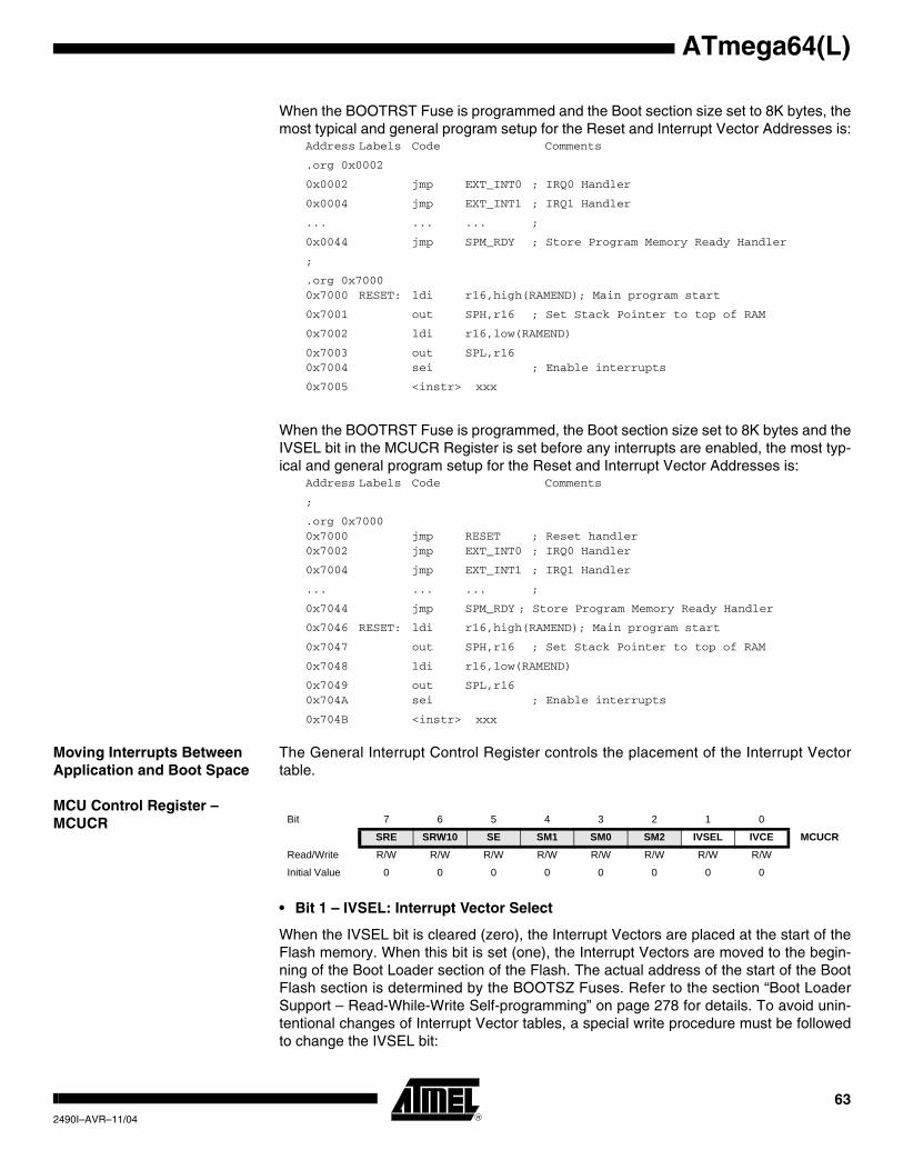
ATmega64(L)
When the BOOTRST Fuse is programmed and the Boot section size set to 8K bytes, themost typical and general program setup for the Reset and Interrupt Vector Addresses is:
Address Labels Code Comments
.org 0x0002
0x0002 jmp EXT_INT0 ; IRQ0 Handler
0x0004 jmp EXT_INT1 ; IRQ1 Handler
... ... ... ;
0x0044 jmp SPM_RDY ; Store Program Memory Ready Handler
;
.org 0x70000x7000 RESET: ldi r16,high(RAMEND); Main program start
0x7001 out SPH,r16 ; Set Stack Pointer to top of RAM
0x7002 ldi r16,low(RAMEND)
0x7003 out SPL,r160x7004 sei ; Enable interrupts
0x7005 <instr> xxx
When the BOOTRST Fuse is programmed, the Boot section size set to 8K bytes and theIVSEL bit in the MCUCR Register is set before any interrupts are enabled, the most typ-ical and general program setup for the Reset and Interrupt Vector Addresses is:
Address Labels Code Comments
;
.org 0x70000x7000 jmp RESET ; Reset handler0x7002 jmp EXT_INT0 ; IRQ0 Handler
0x7004 jmp EXT_INT1 ; IRQ1 Handler
... ... ... ;
0x7044 jmp SPM_RDY ; Store Program Memory Ready Handler
0x7046 RESET: ldi r16,high(RAMEND); Main program start
0x7047 out SPH,r16 ; Set Stack Pointer to top of RAM
0x7048 ldi r16,low(RAMEND)
0x7049 out SPL,r160x704A sei ; Enable interrupts
0x704B <instr> xxx
Moving Interrupts Between Application and Boot Space
The General Interrupt Control Register controls the placement of the Interrupt Vectortable.
MCU Control Register – MCUCR
• Bit 1 – IVSEL: Interrupt Vector Select
When the IVSEL bit is cleared (zero), the Interrupt Vectors are placed at the start of theFlash memory. When this bit is set (one), the Interrupt Vectors are moved to the begin-ning of the Boot Loader section of the Flash. The actual address of the start of the BootFlash section is determined by the BOOTSZ Fuses. Refer to the section “Boot LoaderSupport – Read-While-Write Self-programming” on page 278 for details. To avoid unin-tentional changes of Interrupt Vector tables, a special write procedure must be followedto change the IVSEL bit:
Bit 7 6 5 4 3 2 1 0
SRE SRW10 SE SM1 SM0 SM2 IVSEL IVCE MCUCRRead/Write R/W R/W R/W R/W R/W R/W R/W R/W
Initial Value 0 0 0 0 0 0 0 0
632490I–AVR–11/04
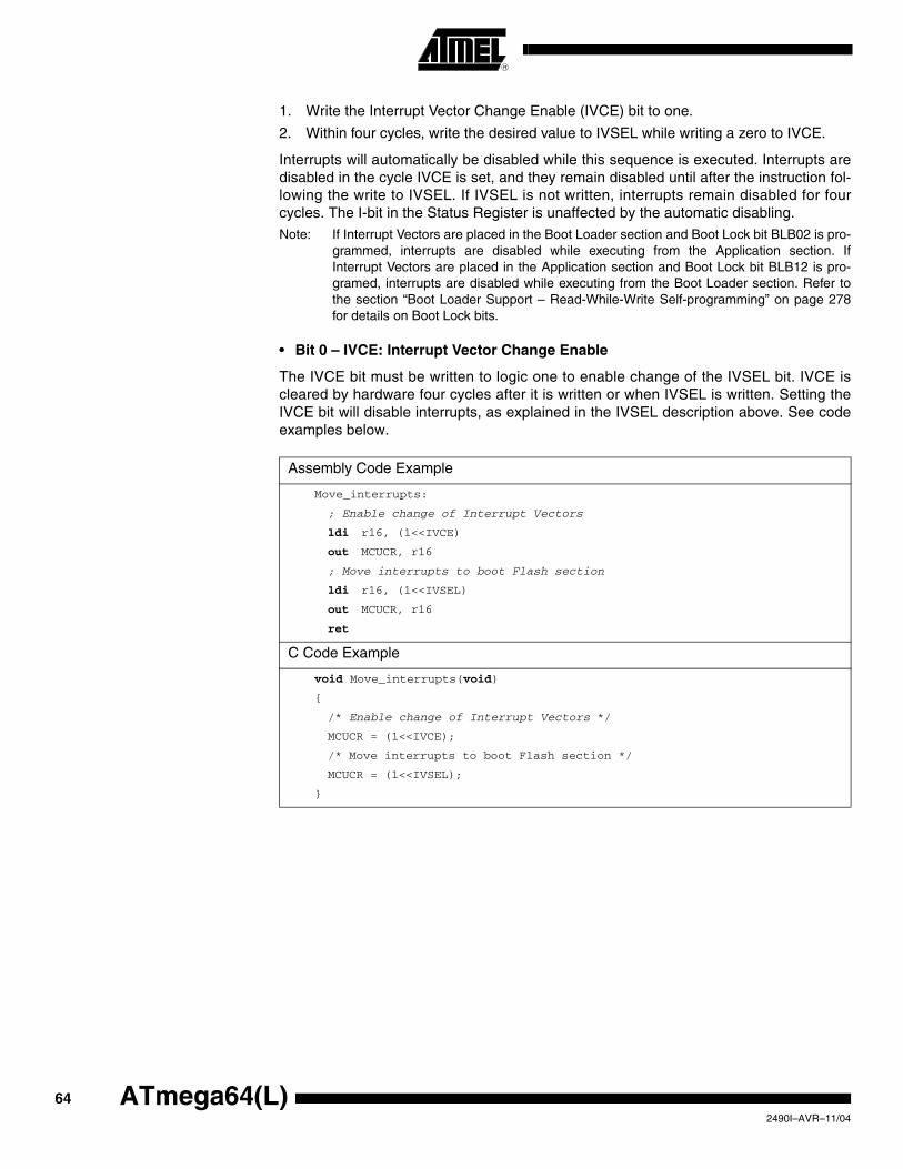
1. Write the Interrupt Vector Change Enable (IVCE) bit to one.
2. Within four cycles, write the desired value to IVSEL while writing a zero to IVCE.
Interrupts will automatically be disabled while this sequence is executed. Interrupts aredisabled in the cycle IVCE is set, and they remain disabled until after the instruction fol-lowing the write to IVSEL. If IVSEL is not written, interrupts remain disabled for fourcycles. The I-bit in the Status Register is unaffected by the automatic disabling.Note: If Interrupt Vectors are placed in the Boot Loader section and Boot Lock bit BLB02 is pro-
grammed, interrupts are disabled while executing from the Application section. IfInterrupt Vectors are placed in the Application section and Boot Lock bit BLB12 is pro-gramed, interrupts are disabled while executing from the Boot Loader section. Refer tothe section “Boot Loader Support – Read-While-Write Self-programming” on page 278for details on Boot Lock bits.
• Bit 0 – IVCE: Interrupt Vector Change Enable
The IVCE bit must be written to logic one to enable change of the IVSEL bit. IVCE iscleared by hardware four cycles after it is written or when IVSEL is written. Setting theIVCE bit will disable interrupts, as explained in the IVSEL description above. See codeexamples below.
Assembly Code Example
Move_interrupts:
; Enable change of Interrupt Vectors
ldi r16, (1<<IVCE)
out MCUCR, r16
; Move interrupts to boot Flash section
ldi r16, (1<<IVSEL)
out MCUCR, r16
ret
C Code Example
void Move_interrupts(void)
/* Enable change of Interrupt Vectors */
MCUCR = (1<<IVCE);
/* Move interrupts to boot Flash section */
MCUCR = (1<<IVSEL);
64 ATmega64(L)2490I–AVR–11/04
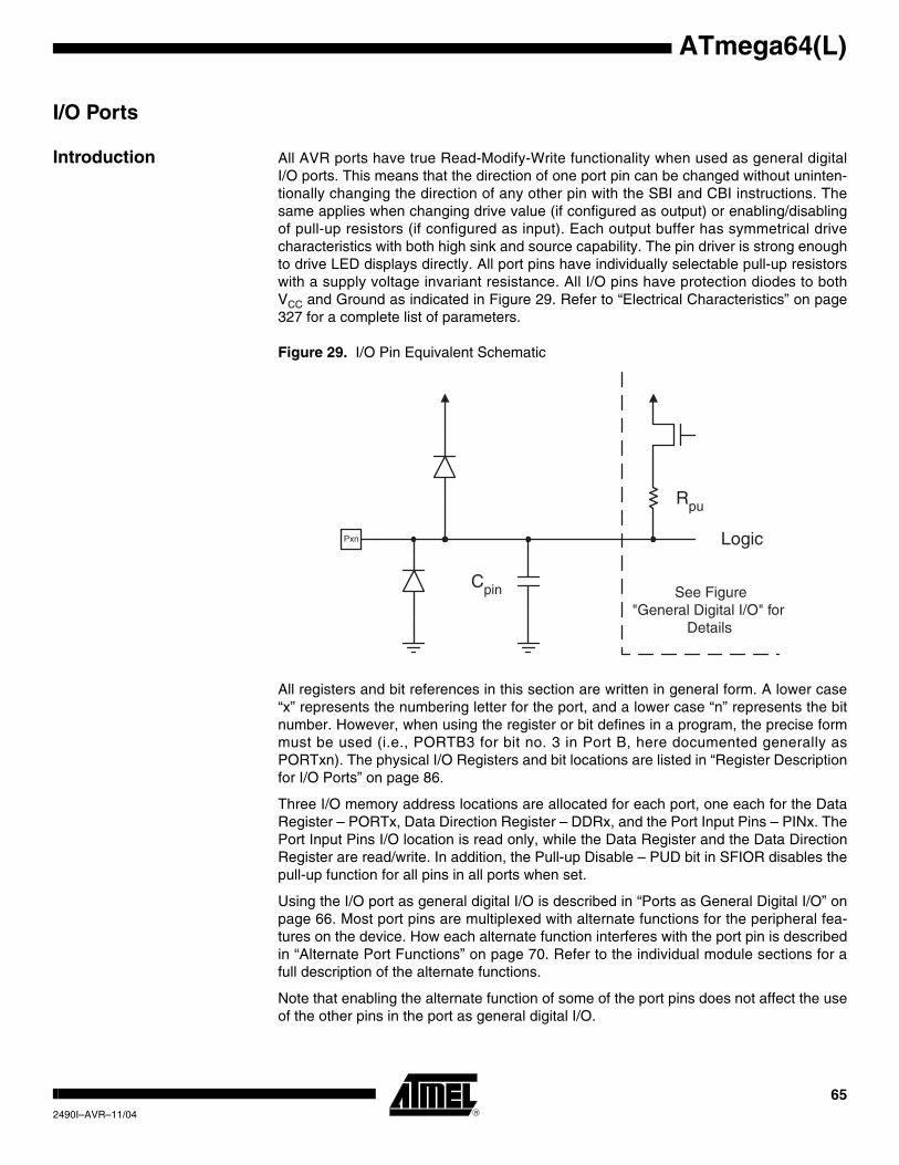
ATmega64(L)
I/O Ports
Introduction All AVR ports have true Read-Modify-Write functionality when used as general digitalI/O ports. This means that the direction of one port pin can be changed without uninten-tionally changing the direction of any other pin with the SBI and CBI instructions. Thesame applies when changing drive value (if configured as output) or enabling/disablingof pull-up resistors (if configured as input). Each output buffer has symmetrical drivecharacteristics with both high sink and source capability. The pin driver is strong enoughto drive LED displays directly. All port pins have individually selectable pull-up resistorswith a supply voltage invariant resistance. All I/O pins have protection diodes to bothVCC and Ground as indicated in Figure 29. Refer to “Electrical Characteristics” on page327 for a complete list of parameters.
Figure 29. I/O Pin Equivalent Schematic
All registers and bit references in this section are written in general form. A lower case“x” represents the numbering letter for the port, and a lower case “n” represents the bitnumber. However, when using the register or bit defines in a program, the precise formmust be used (i.e., PORTB3 for bit no. 3 in Port B, here documented generally asPORTxn). The physical I/O Registers and bit locations are listed in “Register Descriptionfor I/O Ports” on page 86.
Three I/O memory address locations are allocated for each port, one each for the DataRegister – PORTx, Data Direction Register – DDRx, and the Port Input Pins – PINx. ThePort Input Pins I/O location is read only, while the Data Register and the Data DirectionRegister are read/write. In addition, the Pull-up Disable – PUD bit in SFIOR disables thepull-up function for all pins in all ports when set.
Using the I/O port as general digital I/O is described in “Ports as General Digital I/O” onpage 66. Most port pins are multiplexed with alternate functions for the peripheral fea-tures on the device. How each alternate function interferes with the port pin is describedin “Alternate Port Functions” on page 70. Refer to the individual module sections for afull description of the alternate functions.
Note that enabling the alternate function of some of the port pins does not affect the useof the other pins in the port as general digital I/O.
Cpin
Logic
Rpu
See Figure"General Digital I/O" for
Details
Pxn
652490I–AVR–11/04
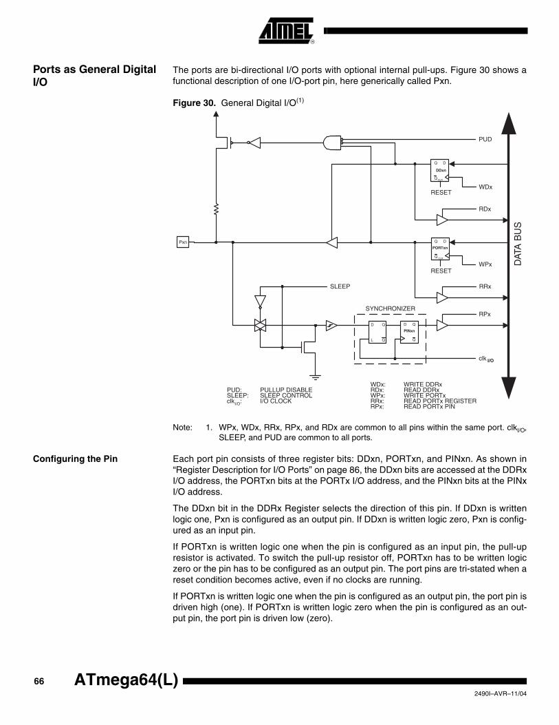
Ports as General Digital I/O
The ports are bi-directional I/O ports with optional internal pull-ups. Figure 30 shows afunctional description of one I/O-port pin, here generically called Pxn.
Figure 30. General Digital I/O(1)
Note: 1. WPx, WDx, RRx, RPx, and RDx are common to all pins within the same port. clkI/O,SLEEP, and PUD are common to all ports.
Configuring the Pin Each port pin consists of three register bits: DDxn, PORTxn, and PINxn. As shown in“Register Description for I/O Ports” on page 86, the DDxn bits are accessed at the DDRxI/O address, the PORTxn bits at the PORTx I/O address, and the PINxn bits at the PINxI/O address.
The DDxn bit in the DDRx Register selects the direction of this pin. If DDxn is writtenlogic one, Pxn is configured as an output pin. If DDxn is written logic zero, Pxn is config-ured as an input pin.
If PORTxn is written logic one when the pin is configured as an input pin, the pull-upresistor is activated. To switch the pull-up resistor off, PORTxn has to be written logiczero or the pin has to be configured as an output pin. The port pins are tri-stated when areset condition becomes active, even if no clocks are running.
If PORTxn is written logic one when the pin is configured as an output pin, the port pin isdriven high (one). If PORTxn is written logic zero when the pin is configured as an out-put pin, the port pin is driven low (zero).
clk
RPx
RRx
WPx
RDx
WDx
PUD
SYNCHRONIZER
WDx: WRITE DDRx
WPx: WRITE PORTxRRx: READ PORTx REGISTERRPx: READ PORTx PIN
PUD: PULLUP DISABLE
clkI/O: I/O CLOCK
RDx: READ DDRx
D
L
Q
Q
RESET
RESET
Q
QD
Q
Q D
CLR
PORTxn
Q
Q D
CLR
DDxn
PINxn
DAT
A B
US
SLEEP
SLEEP: SLEEP CONTROL
Pxn
I/O
66 ATmega64(L)2490I–AVR–11/04
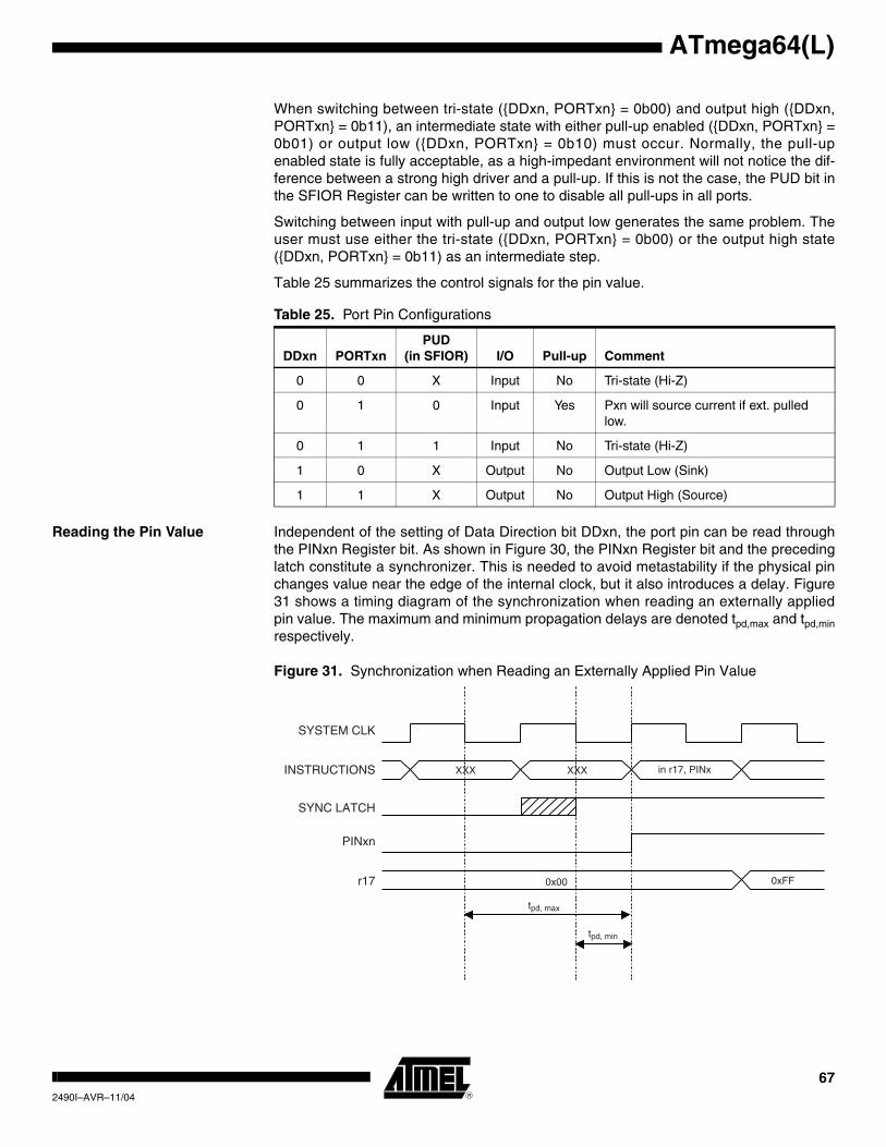
ATmega64(L)
When switching between tri-state (DDxn, PORTxn = 0b00) and output high (DDxn,PORTxn = 0b11), an intermediate state with either pull-up enabled (DDxn, PORTxn =0b01) or output low (DDxn, PORTxn = 0b10) must occur. Normally, the pull-upenabled state is fully acceptable, as a high-impedant environment will not notice the dif-ference between a strong high driver and a pull-up. If this is not the case, the PUD bit inthe SFIOR Register can be written to one to disable all pull-ups in all ports.
Switching between input with pull-up and output low generates the same problem. Theuser must use either the tri-state (DDxn, PORTxn = 0b00) or the output high state(DDxn, PORTxn = 0b11) as an intermediate step.
Table 25 summarizes the control signals for the pin value.
Reading the Pin Value Independent of the setting of Data Direction bit DDxn, the port pin can be read throughthe PINxn Register bit. As shown in Figure 30, the PINxn Register bit and the precedinglatch constitute a synchronizer. This is needed to avoid metastability if the physical pinchanges value near the edge of the internal clock, but it also introduces a delay. Figure31 shows a timing diagram of the synchronization when reading an externally appliedpin value. The maximum and minimum propagation delays are denoted tpd,max and tpd,minrespectively.
Figure 31. Synchronization when Reading an Externally Applied Pin Value
Table 25. Port Pin Configurations
DDxn PORTxnPUD
(in SFIOR) I/O Pull-up Comment
0 0 X Input No Tri-state (Hi-Z)
0 1 0 Input Yes Pxn will source current if ext. pulled low.
0 1 1 Input No Tri-state (Hi-Z)
1 0 X Output No Output Low (Sink)
1 1 X Output No Output High (Source)
SYSTEM CLK
INSTRUCTIONS
SYNC LATCH
PINxn
r17
in r17, PINx
0xFF0x00
tpd, max
XXXXXX
tpd, min
672490I–AVR–11/04
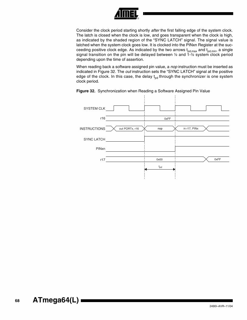
Consider the clock period starting shortly after the first falling edge of the system clock.The latch is closed when the clock is low, and goes transparent when the clock is high,as indicated by the shaded region of the “SYNC LATCH” signal. The signal value islatched when the system clock goes low. It is clocked into the PINxn Register at the suc-ceeding positive clock edge. As indicated by the two arrows tpd,max and tpd,min, a singlesignal transition on the pin will be delayed between ½ and 1-½ system clock perioddepending upon the time of assertion.
When reading back a software assigned pin value, a nop instruction must be inserted asindicated in Figure 32. The out instruction sets the “SYNC LATCH” signal at the positiveedge of the clock. In this case, the delay tpd through the synchronizer is one systemclock period.
Figure 32. Synchronization when Reading a Software Assigned Pin Value
nop in r17, PINx
0xFF
0x00 0xFF
tpd
out PORTx, r16
SYSTEM CLK
r16
INSTRUCTIONS
SYNC LATCH
PINxn
r17
68 ATmega64(L)2490I–AVR–11/04
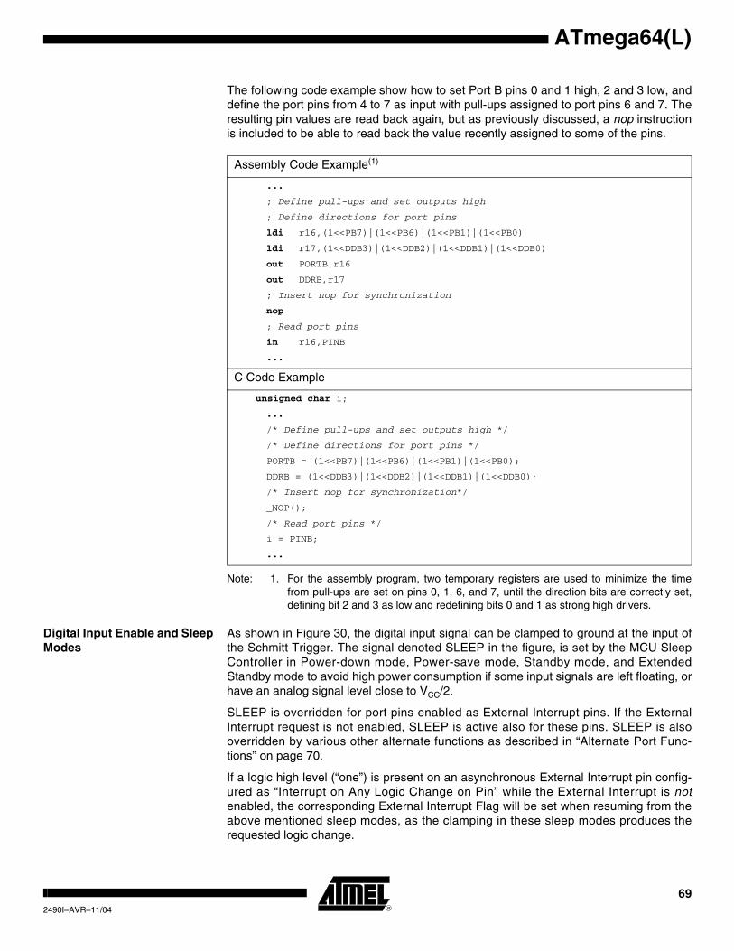
ATmega64(L)
The following code example show how to set Port B pins 0 and 1 high, 2 and 3 low, anddefine the port pins from 4 to 7 as input with pull-ups assigned to port pins 6 and 7. Theresulting pin values are read back again, but as previously discussed, a nop instructionis included to be able to read back the value recently assigned to some of the pins.
Note: 1. For the assembly program, two temporary registers are used to minimize the timefrom pull-ups are set on pins 0, 1, 6, and 7, until the direction bits are correctly set,defining bit 2 and 3 as low and redefining bits 0 and 1 as strong high drivers.
Digital Input Enable and Sleep Modes
As shown in Figure 30, the digital input signal can be clamped to ground at the input ofthe Schmitt Trigger. The signal denoted SLEEP in the figure, is set by the MCU SleepController in Power-down mode, Power-save mode, Standby mode, and ExtendedStandby mode to avoid high power consumption if some input signals are left floating, orhave an analog signal level close to VCC/2.
SLEEP is overridden for port pins enabled as External Interrupt pins. If the ExternalInterrupt request is not enabled, SLEEP is active also for these pins. SLEEP is alsooverridden by various other alternate functions as described in “Alternate Port Func-tions” on page 70.
If a logic high level (“one”) is present on an asynchronous External Interrupt pin config-ured as “Interrupt on Any Logic Change on Pin” while the External Interrupt is notenabled, the corresponding External Interrupt Flag will be set when resuming from theabove mentioned sleep modes, as the clamping in these sleep modes produces therequested logic change.
Assembly Code Example(1)
...
; Define pull-ups and set outputs high
; Define directions for port pins
ldi r16,(1<<PB7)|(1<<PB6)|(1<<PB1)|(1<<PB0)
ldi r17,(1<<DDB3)|(1<<DDB2)|(1<<DDB1)|(1<<DDB0)
out PORTB,r16
out DDRB,r17
; Insert nop for synchronization
nop
; Read port pins
in r16,PINB
...
C Code Example
unsigned char i;
...
/* Define pull-ups and set outputs high */
/* Define directions for port pins */
PORTB = (1<<PB7)|(1<<PB6)|(1<<PB1)|(1<<PB0);
DDRB = (1<<DDB3)|(1<<DDB2)|(1<<DDB1)|(1<<DDB0);
/* Insert nop for synchronization*/
_NOP();
/* Read port pins */
i = PINB;
...
692490I–AVR–11/04
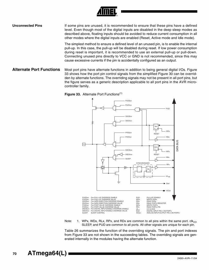
Unconnected Pins If some pins are unused, it is recommended to ensure that these pins have a definedlevel. Even though most of the digital inputs are disabled in the deep sleep modes asdescribed above, floating inputs should be avoided to reduce current consumption in allother modes where the digital inputs are enabled (Reset, Active mode and Idle mode).
The simplest method to ensure a defined level of an unused pin, is to enable the internalpull-up. In this case, the pull-up will be disabled during reset. If low power consumptionduring reset is important, it is recommended to use an external pull-up or pull-down.Connecting unused pins directly to VCC or GND is not recommended, since this maycause excessive currents if the pin is accidentally configured as an output.
Alternate Port Functions Most port pins have alternate functions in addition to being general digital I/Os. Figure33 shows how the port pin control signals from the simplified Figure 30 can be overrid-den by alternate functions. The overriding signals may not be present in all port pins, butthe figure serves as a generic description applicable to all port pins in the AVR micro-controller family.
Figure 33. Alternate Port Functions(1)
Note: 1. WPx, WDx, RLx, RPx, and RDx are common to all pins within the same port. clkI/O,SLEEP, and PUD are common to all ports. All other signals are unique for each pin.
Table 26 summarizes the function of the overriding signals. The pin and port indexesfrom Figure 33 are not shown in the succeeding tables. The overriding signals are gen-erated internally in the modules having the alternate function.
clk
RPx
RRx
WPx
RDx
WDx
PUD
SYNCHRONIZER
WDx: WRITE DDRx
WPx: WRITE PORTxRRx: READ PORTx REGISTER
RPx: READ PORTx PIN
PUD: PULLUP DISABLE
clkI/O: I/O CLOCK
RDx: READ DDRx
D
L
Q
Q
SET
CLR
0
1
0
1
0
1
DIxn
AIOxn
DIEOExn
PVOVxn
PVOExn
DDOVxn
DDOExn
PUOExn
PUOVxn
PUOExn: Pxn PULL-UP OVERRIDE ENABLEPUOVxn: Pxn PULL-UP OVERRIDE VALUEDDOExn: Pxn DATA DIRECTION OVERRIDE ENABLEDDOVxn: Pxn DATA DIRECTION OVERRIDE VALUEPVOExn: Pxn PORT VALUE OVERRIDE ENABLEPVOVxn: Pxn PORT VALUE OVERRIDE VALUE
DIxn: DIGITAL INPUT PIN n ON PORTxAIOxn: ANALOG INPUT/OUTPUT PIN n ON PORTx
RESET
RESET
Q
Q D
CLR
Q
Q D
CLR
Q
QD
CLR
PINxn
PORTxn
DDxn
DAT
A B
US
0
1DIEOVxn
SLEEP
DIEOExn: Pxn DIGITAL INPUT-ENABLE OVERRIDE ENABLEDIEOVxn: Pxn DIGITAL INPUT-ENABLE OVERRIDE VALUESLEEP: SLEEP CONTROL
Pxn
I/O
70 ATmega64(L)2490I–AVR–11/04
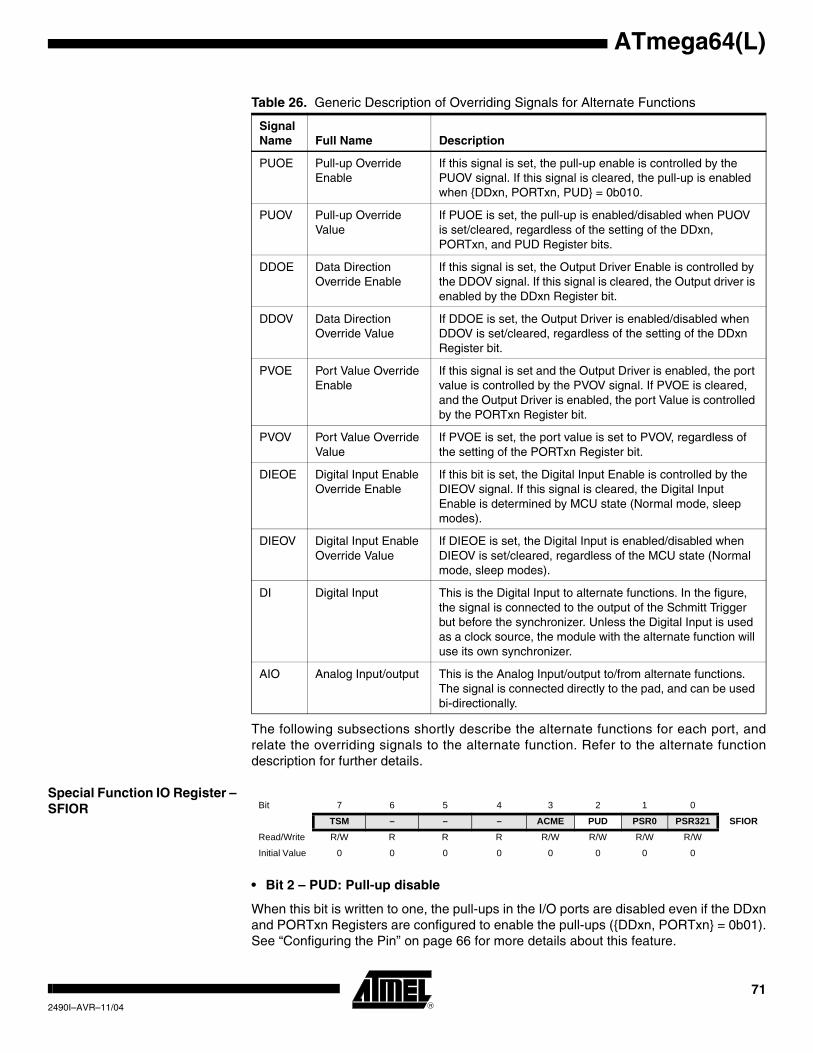
ATmega64(L)
The following subsections shortly describe the alternate functions for each port, andrelate the overriding signals to the alternate function. Refer to the alternate functiondescription for further details.
Special Function IO Register – SFIOR
• Bit 2 – PUD: Pull-up disable
When this bit is written to one, the pull-ups in the I/O ports are disabled even if the DDxnand PORTxn Registers are configured to enable the pull-ups (DDxn, PORTxn = 0b01).See “Configuring the Pin” on page 66 for more details about this feature.
Table 26. Generic Description of Overriding Signals for Alternate Functions
Signal Name Full Name Description
PUOE Pull-up Override Enable
If this signal is set, the pull-up enable is controlled by the PUOV signal. If this signal is cleared, the pull-up is enabled when DDxn, PORTxn, PUD = 0b010.
PUOV Pull-up Override Value
If PUOE is set, the pull-up is enabled/disabled when PUOV is set/cleared, regardless of the setting of the DDxn, PORTxn, and PUD Register bits.
DDOE Data Direction Override Enable
If this signal is set, the Output Driver Enable is controlled by the DDOV signal. If this signal is cleared, the Output driver is enabled by the DDxn Register bit.
DDOV Data Direction Override Value
If DDOE is set, the Output Driver is enabled/disabled when DDOV is set/cleared, regardless of the setting of the DDxn Register bit.
PVOE Port Value Override Enable
If this signal is set and the Output Driver is enabled, the port value is controlled by the PVOV signal. If PVOE is cleared, and the Output Driver is enabled, the port Value is controlled by the PORTxn Register bit.
PVOV Port Value Override Value
If PVOE is set, the port value is set to PVOV, regardless of the setting of the PORTxn Register bit.
DIEOE Digital Input Enable Override Enable
If this bit is set, the Digital Input Enable is controlled by the DIEOV signal. If this signal is cleared, the Digital Input Enable is determined by MCU state (Normal mode, sleep modes).
DIEOV Digital Input Enable Override Value
If DIEOE is set, the Digital Input is enabled/disabled when DIEOV is set/cleared, regardless of the MCU state (Normal mode, sleep modes).
DI Digital Input This is the Digital Input to alternate functions. In the figure, the signal is connected to the output of the Schmitt Trigger but before the synchronizer. Unless the Digital Input is used as a clock source, the module with the alternate function will use its own synchronizer.
AIO Analog Input/output This is the Analog Input/output to/from alternate functions. The signal is connected directly to the pad, and can be used bi-directionally.
Bit 7 6 5 4 3 2 1 0
TSM – – – ACME PUD PSR0 PSR321 SFIORRead/Write R/W R R R R/W R/W R/W R/W
Initial Value 0 0 0 0 0 0 0 0
712490I–AVR–11/04
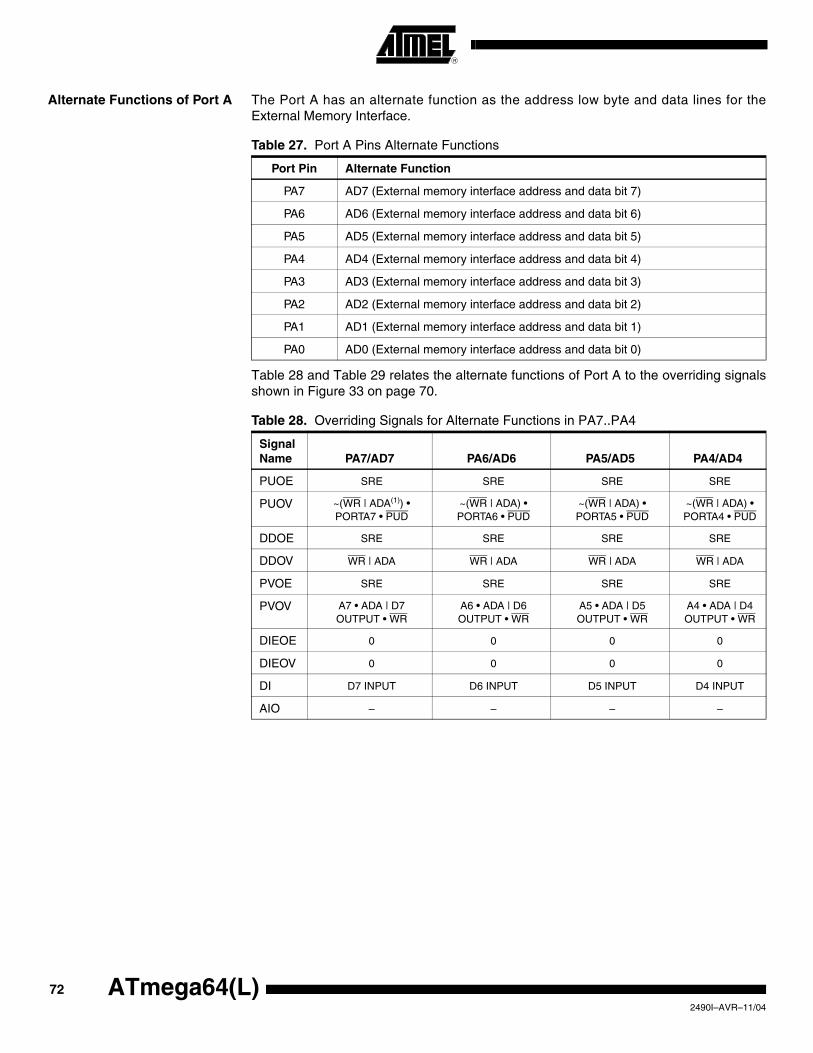
Alternate Functions of Port A The Port A has an alternate function as the address low byte and data lines for theExternal Memory Interface.
Table 28 and Table 29 relates the alternate functions of Port A to the overriding signalsshown in Figure 33 on page 70.
Table 27. Port A Pins Alternate Functions
Port Pin Alternate Function
PA7 AD7 (External memory interface address and data bit 7)
PA6 AD6 (External memory interface address and data bit 6)
PA5 AD5 (External memory interface address and data bit 5)
PA4 AD4 (External memory interface address and data bit 4)
PA3 AD3 (External memory interface address and data bit 3)
PA2 AD2 (External memory interface address and data bit 2)
PA1 AD1 (External memory interface address and data bit 1)
PA0 AD0 (External memory interface address and data bit 0)
Table 28. Overriding Signals for Alternate Functions in PA7..PA4
Signal Name PA7/AD7 PA6/AD6 PA5/AD5 PA4/AD4
PUOE SRE SRE SRE SRE
PUOV ~(WR | ADA(1)) • PORTA7 • PUD
~(WR | ADA) • PORTA6 • PUD
~(WR | ADA) • PORTA5 • PUD
~(WR | ADA) • PORTA4 • PUD
DDOE SRE SRE SRE SRE
DDOV WR | ADA WR | ADA WR | ADA WR | ADA
PVOE SRE SRE SRE SRE
PVOV A7 • ADA | D7 OUTPUT • WR
A6 • ADA | D6 OUTPUT • WR
A5 • ADA | D5 OUTPUT • WR
A4 • ADA | D4 OUTPUT • WR
DIEOE 0 0 0 0
DIEOV 0 0 0 0
DI D7 INPUT D6 INPUT D5 INPUT D4 INPUT
AIO – – – –
72 ATmega64(L)2490I–AVR–11/04
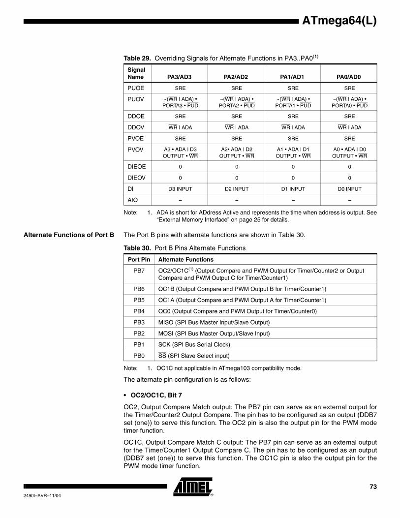
ATmega64(L)
Note: 1. ADA is short for ADdress Active and represents the time when address is output. See“External Memory Interface” on page 25 for details.
Alternate Functions of Port B The Port B pins with alternate functions are shown in Table 30.
Note: 1. OC1C not applicable in ATmega103 compatibility mode.
The alternate pin configuration is as follows:
• OC2/OC1C, Bit 7
OC2, Output Compare Match output: The PB7 pin can serve as an external output forthe Timer/Counter2 Output Compare. The pin has to be configured as an output (DDB7set (one)) to serve this function. The OC2 pin is also the output pin for the PWM modetimer function.
OC1C, Output Compare Match C output: The PB7 pin can serve as an external outputfor the Timer/Counter1 Output Compare C. The pin has to be configured as an output(DDB7 set (one)) to serve this function. The OC1C pin is also the output pin for thePWM mode timer function.
Table 29. Overriding Signals for Alternate Functions in PA3..PA0(1)
Signal Name PA3/AD3 PA2/AD2 PA1/AD1 PA0/AD0
PUOE SRE SRE SRE SRE
PUOV ~(WR | ADA) • PORTA3 • PUD
~(WR | ADA) • PORTA2 • PUD
~(WR | ADA) • PORTA1 • PUD
~(WR | ADA) • PORTA0 • PUD
DDOE SRE SRE SRE SRE
DDOV WR | ADA WR | ADA WR | ADA WR | ADA
PVOE SRE SRE SRE SRE
PVOV A3 • ADA | D3 OUTPUT • WR
A2• ADA | D2 OUTPUT • WR
A1 • ADA | D1 OUTPUT • WR
A0 • ADA | D0 OUTPUT • WR
DIEOE 0 0 0 0
DIEOV 0 0 0 0
DI D3 INPUT D2 INPUT D1 INPUT D0 INPUT
AIO – – – –
Table 30. Port B Pins Alternate Functions
Port Pin Alternate Functions
PB7 OC2/OC1C(1) (Output Compare and PWM Output for Timer/Counter2 or Output Compare and PWM Output C for Timer/Counter1)
PB6 OC1B (Output Compare and PWM Output B for Timer/Counter1)
PB5 OC1A (Output Compare and PWM Output A for Timer/Counter1)
PB4 OC0 (Output Compare and PWM Output for Timer/Counter0)
PB3 MISO (SPI Bus Master Input/Slave Output)
PB2 MOSI (SPI Bus Master Output/Slave Input)
PB1 SCK (SPI Bus Serial Clock)
PB0 SS (SPI Slave Select input)
732490I–AVR–11/04
• OC1B, Bit 6
OC1B, Output Compare Match B output: The PB6 pin can serve as an external outputfor the Timer/Counter1 Output Compare B. The pin has to be configured as an output(DDB6 set (one)) to serve this function. The OC1B pin is also the output pin for the PWMmode timer function.
• OC1A, Bit 5
OC1A, Output Compare Match A output: The PB5 pin can serve as an external outputfor the Timer/Counter1 Output Compare A. The pin has to be configured as an output(DDB5 set (one)) to serve this function. The OC1A pin is also the output pin for the PWMmode timer function.
• OC0, Bit 4
OC0, Output Compare Match output: The PB4 pin can serve as an external output forthe Timer/Counter0 Output Compare. The pin has to be configured as an output (DDB4set (one)) to serve this function. The OC0 pin is also the output pin for the PWM modetimer function.
• MISO – Port B, Bit 3
MISO: Master Data input, Slave Data output pin for SPI channel. When the SPI isenabled as a Master, this pin is configured as an input regardless of the setting ofDDB3. When the SPI is enabled as a Slave, the data direction of this pin is controlled byDDB3. When the pin is forced to be an input, the pull-up can still be controlled by thePORTB3 bit.
• MOSI – Port B, Bit 2
MOSI: SPI Master Data output, Slave Data input for SPI channel. When the SPI isenabled as a Slave, this pin is configured as an input regardless of the setting of DDB2.When the SPI is enabled as a Master, the data direction of this pin is controlled byDDB2. When the pin is forced to be an input, the pull-up can still be controlled by thePORTB2 bit.
• SCK – Port B, Bit 1
SCK: Master Clock output, Slave Clock input pin for SPI channel. When the SPI isenabled as a Slave, this pin is configured as an input regardless of the setting of DDB1.When the SPI is enabled as a Master, the data direction of this pin is controlled byDDB1. When the pin is forced to be an input, the pull-up can still be controlled by thePORTB1 bit.
• SS – Port B, Bit 0
SS: Slave Port Select input. When the SPI is enabled as a Slave, this pin is configuredas an input regardless of the setting of DDB0. As a Slave, the SPI is activated when thispin is driven low. When the SPI is enabled as a Master, the data direction of this pin iscontrolled by DDB0. When the pin is forced to be an input, the pull-up can still be con-trolled by the PORTB0 bit.
Table 31 and Table 32 relate the alternate functions of Port B to the overriding signalsshown in Figure 33 on page 70. SPI MSTR INPUT and SPI SLAVE OUTPUT constitutethe MISO signal, while MOSI is divided into SPI MSTR OUTPUT and SPI SLAVEINPUT.
74 ATmega64(L)2490I–AVR–11/04
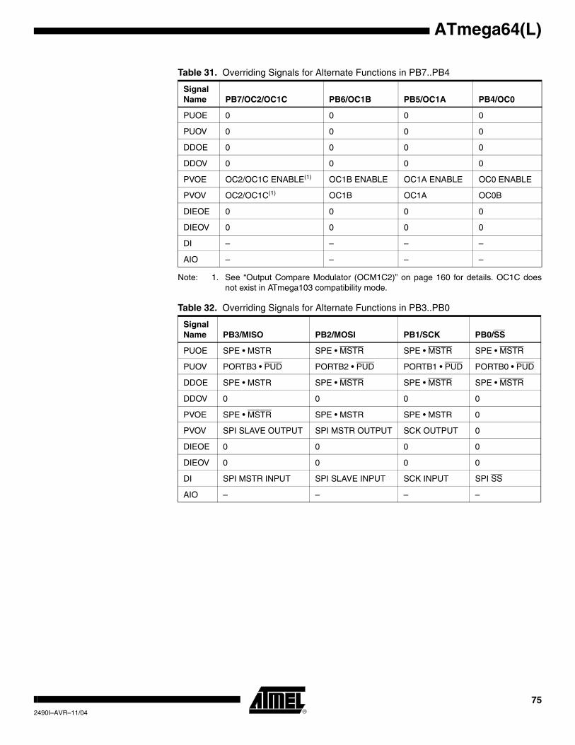
ATmega64(L)
Note: 1. See “Output Compare Modulator (OCM1C2)” on page 160 for details. OC1C doesnot exist in ATmega103 compatibility mode.
Table 31. Overriding Signals for Alternate Functions in PB7..PB4
Signal Name PB7/OC2/OC1C PB6/OC1B PB5/OC1A PB4/OC0
PUOE 0 0 0 0
PUOV 0 0 0 0
DDOE 0 0 0 0
DDOV 0 0 0 0
PVOE OC2/OC1C ENABLE(1) OC1B ENABLE OC1A ENABLE OC0 ENABLE
PVOV OC2/OC1C(1) OC1B OC1A OC0B
DIEOE 0 0 0 0
DIEOV 0 0 0 0
DI – – – –
AIO – – – –
Table 32. Overriding Signals for Alternate Functions in PB3..PB0
Signal Name PB3/MISO PB2/MOSI PB1/SCK PB0/SS
PUOE SPE • MSTR SPE • MSTR SPE • MSTR SPE • MSTR
PUOV PORTB3 • PUD PORTB2 • PUD PORTB1 • PUD PORTB0 • PUD
DDOE SPE • MSTR SPE • MSTR SPE • MSTR SPE • MSTR
DDOV 0 0 0 0
PVOE SPE • MSTR SPE • MSTR SPE • MSTR 0
PVOV SPI SLAVE OUTPUT SPI MSTR OUTPUT SCK OUTPUT 0
DIEOE 0 0 0 0
DIEOV 0 0 0 0
DI SPI MSTR INPUT SPI SLAVE INPUT SCK INPUT SPI SS
AIO – – – –
752490I–AVR–11/04
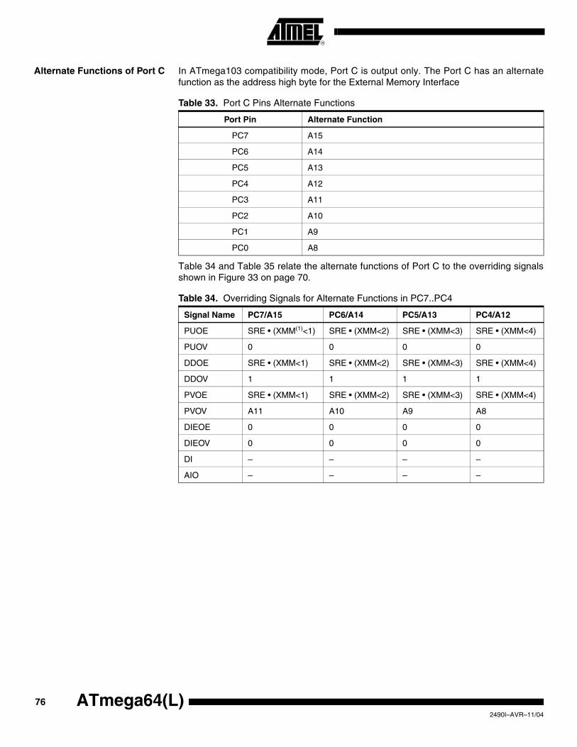
Alternate Functions of Port C In ATmega103 compatibility mode, Port C is output only. The Port C has an alternatefunction as the address high byte for the External Memory Interface
Table 34 and Table 35 relate the alternate functions of Port C to the overriding signalsshown in Figure 33 on page 70.
Table 33. Port C Pins Alternate Functions
Port Pin Alternate Function
PC7 A15
PC6 A14
PC5 A13
PC4 A12
PC3 A11
PC2 A10
PC1 A9
PC0 A8
Table 34. Overriding Signals for Alternate Functions in PC7..PC4
Signal Name PC7/A15 PC6/A14 PC5/A13 PC4/A12
PUOE SRE • (XMM(1)<1) SRE • (XMM<2) SRE • (XMM<3) SRE • (XMM<4)
PUOV 0 0 0 0
DDOE SRE • (XMM<1) SRE • (XMM<2) SRE • (XMM<3) SRE • (XMM<4)
DDOV 1 1 1 1
PVOE SRE • (XMM<1) SRE • (XMM<2) SRE • (XMM<3) SRE • (XMM<4)
PVOV A11 A10 A9 A8
DIEOE 0 0 0 0
DIEOV 0 0 0 0
DI – – – –
AIO – – – –
76 ATmega64(L)2490I–AVR–11/04
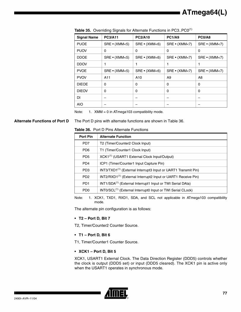
ATmega64(L)
Note: 1. XMM = 0 in ATmega103 compatibility mode.
Alternate Functions of Port D The Port D pins with alternate functions are shown in Table 36.
Note: 1. XCK1, TXD1, RXD1, SDA, and SCL not applicable in ATmega103 compatibilitymode.
The alternate pin configuration is as follows:
• T2 – Port D, Bit 7
T2, Timer/Counter2 Counter Source.
• T1 – Port D, Bit 6
T1, Timer/Counter1 Counter Source.
• XCK1 – Port D, Bit 5
XCK1, USART1 External Clock. The Data Direction Register (DDD5) controls whetherthe clock is output (DDD5 set) or input (DDD5 cleared). The XCK1 pin is active onlywhen the USART1 operates in synchronous mode.
Table 35. Overriding Signals for Alternate Functions in PC3..PC0(1)
Signal Name PC3/A11 PC2/A10 PC1/A9 PC0/A8
PUOE SRE • (XMM<5) SRE • (XMM<6) SRE • (XMM<7) SRE • (XMM<7)
PUOV 0 0 0 0
DDOE SRE • (XMM<5) SRE • (XMM<6) SRE • (XMM<7) SRE • (XMM<7)
DDOV 1 1 1 1
PVOE SRE • (XMM<5) SRE • (XMM<6) SRE • (XMM<7) SRE • (XMM<7)
PVOV A11 A10 A9 A8
DIEOE 0 0 0 0
DIEOV 0 0 0 0
DI – – – –
AIO – – – –
Table 36. Port D Pins Alternate Functions
Port Pin Alternate Function
PD7 T2 (Timer/Counter2 Clock Input)
PD6 T1 (Timer/Counter1 Clock Input)
PD5 XCK1(1) (USART1 External Clock Input/Output)
PD4 ICP1 (Timer/Counter1 Input Capture Pin)
PD3 INT3/TXD1(1) (External Interrupt3 Input or UART1 Transmit Pin)
PD2 INT2/RXD1(1) (External Interrupt2 Input or UART1 Receive Pin)
PD1 INT1/SDA(1) (External Interrupt1 Input or TWI Serial DAta)
PD0 INT0/SCL(1) (External Interrupt0 Input or TWI Serial CLock)
772490I–AVR–11/04
• ICP1 – Port D, Bit 4
ICP1 – Input Capture Pin1: The PD4 pin can act as an Input Capture pin forTimer/Counter1.
• INT3/TXD1 – Port D, Bit 3
INT3, External Interrupt Source 3: The PD3 pin can serve as an External Interruptsource to the MCU.
TXD1, Transmit Data (Data output pin for the USART1). When the USART1 transmitteris enabled, this pin is configured as an output regardless of the value of DDD3.
• INT2/RXD1 – Port D, Bit 2
INT2, External Interrupt source 2. The PD2 pin can serve as an External Interruptsource to the MCU.
RXD1, Receive Data (Data input pin for the USART1). When the USART1 receiver isenabled this pin is configured as an input regardless of the value of DDD2. When theUSART forces this pin to be an input, the pull-up can still be controlled by the PORTD2bit.
• INT1/SDA – Port D, Bit 1
INT1, External Interrupt Source 1. The PD1 pin can serve as an External Interruptsource to the MCU.
SDA, Two-wire Serial Interface Data: When the TWEN bit in TWCR is set (one) toenable the Two-wire Serial Interface, pin PD1 is disconnected from the port andbecomes the serial data I/O pin for the Two-wire Serial Interface. In this mode, there is aspike filter on the pin to suppress spikes shorter than 50 ns on the input signal, and thepin is driven by an open drain driver with slew-rate limitation.
• INT0/SCL – Port D, Bit 0
INT0, External Interrupt Source 0. The PD0 pin can serve as an External Interruptsource to the MCU.
SCL, Two-wire Serial Interface Clock: When the TWEN bit in TWCR is set (one) toenable the Two-wire Serial Interface, pin PD0 is disconnected from the port andbecomes the serial clock I/O pin for the Two-wire Serial Interface. In this mode, there isa spike filter on the pin to suppress spikes shorter than 50 ns on the input signal, and thepin is driven by an open drain driver with slew-rate limitation.
Table 37 and Table 38 relates the alternate functions of Port D to the overriding signalsshown in Figure 33 on page 70.
78 ATmega64(L)2490I–AVR–11/04
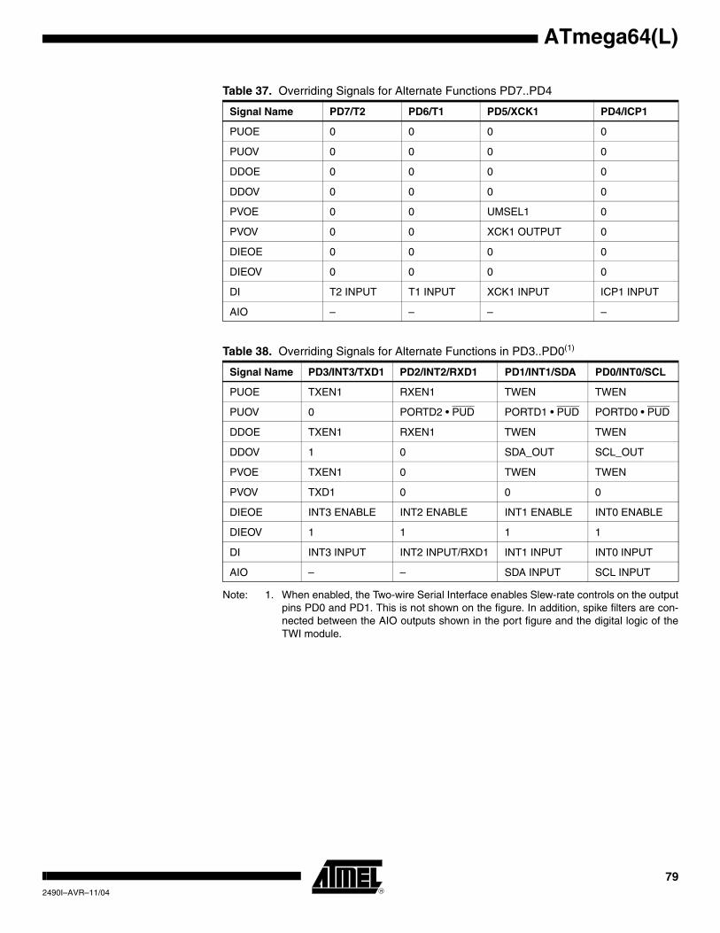
ATmega64(L)
Note: 1. When enabled, the Two-wire Serial Interface enables Slew-rate controls on the outputpins PD0 and PD1. This is not shown on the figure. In addition, spike filters are con-nected between the AIO outputs shown in the port figure and the digital logic of theTWI module.
Table 37. Overriding Signals for Alternate Functions PD7..PD4
Signal Name PD7/T2 PD6/T1 PD5/XCK1 PD4/ICP1
PUOE 0 0 0 0
PUOV 0 0 0 0
DDOE 0 0 0 0
DDOV 0 0 0 0
PVOE 0 0 UMSEL1 0
PVOV 0 0 XCK1 OUTPUT 0
DIEOE 0 0 0 0
DIEOV 0 0 0 0
DI T2 INPUT T1 INPUT XCK1 INPUT ICP1 INPUT
AIO – – – –
Table 38. Overriding Signals for Alternate Functions in PD3..PD0(1)
Signal Name PD3/INT3/TXD1 PD2/INT2/RXD1 PD1/INT1/SDA PD0/INT0/SCL
PUOE TXEN1 RXEN1 TWEN TWEN
PUOV 0 PORTD2 • PUD PORTD1 • PUD PORTD0 • PUD
DDOE TXEN1 RXEN1 TWEN TWEN
DDOV 1 0 SDA_OUT SCL_OUT
PVOE TXEN1 0 TWEN TWEN
PVOV TXD1 0 0 0
DIEOE INT3 ENABLE INT2 ENABLE INT1 ENABLE INT0 ENABLE
DIEOV 1 1 1 1
DI INT3 INPUT INT2 INPUT/RXD1 INT1 INPUT INT0 INPUT
AIO – – SDA INPUT SCL INPUT
792490I–AVR–11/04
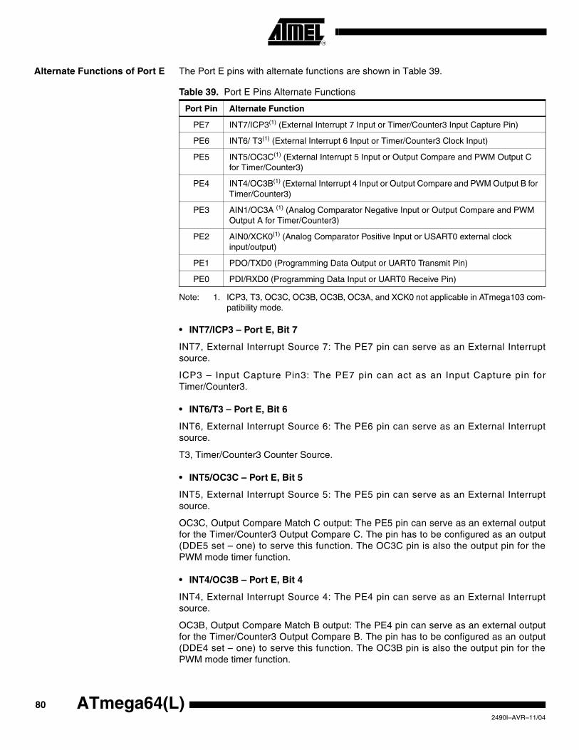
Alternate Functions of Port E The Port E pins with alternate functions are shown in Table 39.
Note: 1. ICP3, T3, OC3C, OC3B, OC3B, OC3A, and XCK0 not applicable in ATmega103 com-patibility mode.
• INT7/ICP3 – Port E, Bit 7
INT7, External Interrupt Source 7: The PE7 pin can serve as an External Interruptsource.
ICP3 – Input Capture Pin3: The PE7 pin can act as an Input Capture pin forTimer/Counter3.
• INT6/T3 – Port E, Bit 6
INT6, External Interrupt Source 6: The PE6 pin can serve as an External Interruptsource.
T3, Timer/Counter3 Counter Source.
• INT5/OC3C – Port E, Bit 5
INT5, External Interrupt Source 5: The PE5 pin can serve as an External Interruptsource.
OC3C, Output Compare Match C output: The PE5 pin can serve as an external outputfor the Timer/Counter3 Output Compare C. The pin has to be configured as an output(DDE5 set – one) to serve this function. The OC3C pin is also the output pin for thePWM mode timer function.
• INT4/OC3B – Port E, Bit 4
INT4, External Interrupt Source 4: The PE4 pin can serve as an External Interruptsource.
OC3B, Output Compare Match B output: The PE4 pin can serve as an external outputfor the Timer/Counter3 Output Compare B. The pin has to be configured as an output(DDE4 set – one) to serve this function. The OC3B pin is also the output pin for thePWM mode timer function.
Table 39. Port E Pins Alternate Functions
Port Pin Alternate Function
PE7 INT7/ICP3(1) (External Interrupt 7 Input or Timer/Counter3 Input Capture Pin)
PE6 INT6/ T3(1) (External Interrupt 6 Input or Timer/Counter3 Clock Input)
PE5 INT5/OC3C(1) (External Interrupt 5 Input or Output Compare and PWM Output C for Timer/Counter3)
PE4 INT4/OC3B(1) (External Interrupt 4 Input or Output Compare and PWM Output B for Timer/Counter3)
PE3 AIN1/OC3A (1) (Analog Comparator Negative Input or Output Compare and PWM Output A for Timer/Counter3)
PE2 AIN0/XCK0(1) (Analog Comparator Positive Input or USART0 external clock input/output)
PE1 PDO/TXD0 (Programming Data Output or UART0 Transmit Pin)
PE0 PDI/RXD0 (Programming Data Input or UART0 Receive Pin)
80 ATmega64(L)2490I–AVR–11/04
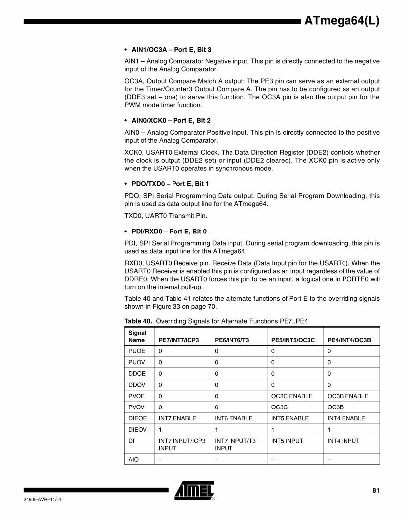
ATmega64(L)
• AIN1/OC3A – Port E, Bit 3
AIN1 – Analog Comparator Negative input. This pin is directly connected to the negativeinput of the Analog Comparator.
OC3A, Output Compare Match A output: The PE3 pin can serve as an external outputfor the Timer/Counter3 Output Compare A. The pin has to be configured as an output(DDE3 set – one) to serve this function. The OC3A pin is also the output pin for thePWM mode timer function.
• AIN0/XCK0 – Port E, Bit 2
AIN0 – Analog Comparator Positive input. This pin is directly connected to the positiveinput of the Analog Comparator.
XCK0, USART0 External Clock. The Data Direction Register (DDE2) controls whetherthe clock is output (DDE2 set) or input (DDE2 cleared). The XCK0 pin is active onlywhen the USART0 operates in synchronous mode.
• PDO/TXD0 – Port E, Bit 1
PDO, SPI Serial Programming Data output. During Serial Program Downloading, thispin is used as data output line for the ATmega64.
TXD0, UART0 Transmit Pin.
• PDI/RXD0 – Port E, Bit 0
PDI, SPI Serial Programming Data input. During serial program downloading, this pin isused as data input line for the ATmega64.
RXD0, USART0 Receive pin. Receive Data (Data Input pin for the USART0). When theUSART0 Receiver is enabled this pin is configured as an input regardless of the value ofDDRE0. When the USART0 forces this pin to be an input, a logical one in PORTE0 willturn on the internal pull-up.
Table 40 and Table 41 relates the alternate functions of Port E to the overriding signalsshown in Figure 33 on page 70.
Table 40. Overriding Signals for Alternate Functions PE7..PE4
Signal Name PE7/INT7/ICP3 PE6/INT6/T3 PE5/INT5/OC3C PE4/INT4/OC3B
PUOE 0 0 0 0
PUOV 0 0 0 0
DDOE 0 0 0 0
DDOV 0 0 0 0
PVOE 0 0 OC3C ENABLE OC3B ENABLE
PVOV 0 0 OC3C OC3B
DIEOE INT7 ENABLE INT6 ENABLE INT5 ENABLE INT4 ENABLE
DIEOV 1 1 1 1
DI INT7 INPUT/ICP3 INPUT
INT7 INPUT/T3 INPUT
INT5 INPUT INT4 INPUT
AIO – – – –
812490I–AVR–11/04
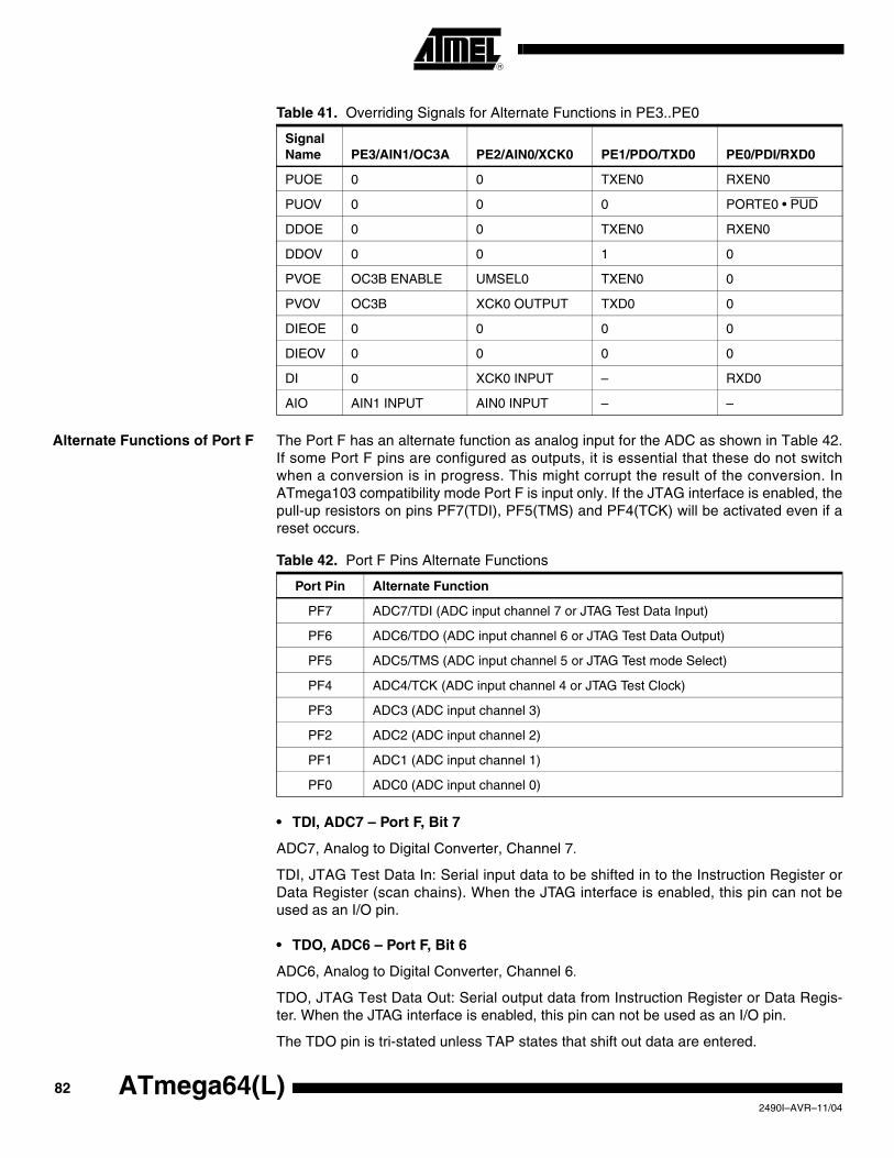
Alternate Functions of Port F The Port F has an alternate function as analog input for the ADC as shown in Table 42.If some Port F pins are configured as outputs, it is essential that these do not switchwhen a conversion is in progress. This might corrupt the result of the conversion. InATmega103 compatibility mode Port F is input only. If the JTAG interface is enabled, thepull-up resistors on pins PF7(TDI), PF5(TMS) and PF4(TCK) will be activated even if areset occurs.
• TDI, ADC7 – Port F, Bit 7
ADC7, Analog to Digital Converter, Channel 7.
TDI, JTAG Test Data In: Serial input data to be shifted in to the Instruction Register orData Register (scan chains). When the JTAG interface is enabled, this pin can not beused as an I/O pin.
• TDO, ADC6 – Port F, Bit 6
ADC6, Analog to Digital Converter, Channel 6.
TDO, JTAG Test Data Out: Serial output data from Instruction Register or Data Regis-ter. When the JTAG interface is enabled, this pin can not be used as an I/O pin.
The TDO pin is tri-stated unless TAP states that shift out data are entered.
Table 41. Overriding Signals for Alternate Functions in PE3..PE0
Signal Name PE3/AIN1/OC3A PE2/AIN0/XCK0 PE1/PDO/TXD0 PE0/PDI/RXD0
PUOE 0 0 TXEN0 RXEN0
PUOV 0 0 0 PORTE0 • PUD
DDOE 0 0 TXEN0 RXEN0
DDOV 0 0 1 0
PVOE OC3B ENABLE UMSEL0 TXEN0 0
PVOV OC3B XCK0 OUTPUT TXD0 0
DIEOE 0 0 0 0
DIEOV 0 0 0 0
DI 0 XCK0 INPUT – RXD0
AIO AIN1 INPUT AIN0 INPUT – –
Table 42. Port F Pins Alternate Functions
Port Pin Alternate Function
PF7 ADC7/TDI (ADC input channel 7 or JTAG Test Data Input)
PF6 ADC6/TDO (ADC input channel 6 or JTAG Test Data Output)
PF5 ADC5/TMS (ADC input channel 5 or JTAG Test mode Select)
PF4 ADC4/TCK (ADC input channel 4 or JTAG Test Clock)
PF3 ADC3 (ADC input channel 3)
PF2 ADC2 (ADC input channel 2)
PF1 ADC1 (ADC input channel 1)
PF0 ADC0 (ADC input channel 0)
82 ATmega64(L)2490I–AVR–11/04
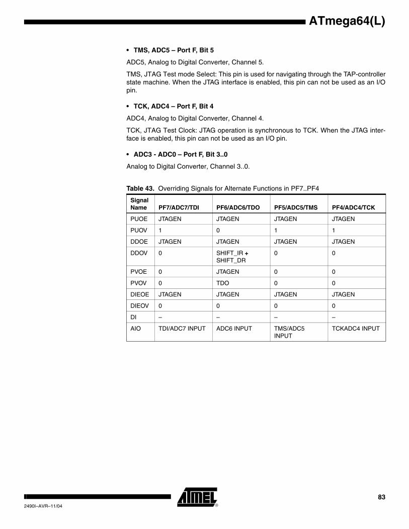
ATmega64(L)
• TMS, ADC5 – Port F, Bit 5
ADC5, Analog to Digital Converter, Channel 5.
TMS, JTAG Test mode Select: This pin is used for navigating through the TAP-controllerstate machine. When the JTAG interface is enabled, this pin can not be used as an I/Opin.
• TCK, ADC4 – Port F, Bit 4
ADC4, Analog to Digital Converter, Channel 4.
TCK, JTAG Test Clock: JTAG operation is synchronous to TCK. When the JTAG inter-face is enabled, this pin can not be used as an I/O pin.
• ADC3 - ADC0 – Port F, Bit 3..0
Analog to Digital Converter, Channel 3..0.
Table 43. Overriding Signals for Alternate Functions in PF7..PF4
Signal Name PF7/ADC7/TDI PF6/ADC6/TDO PF5/ADC5/TMS PF4/ADC4/TCK
PUOE JTAGEN JTAGEN JTAGEN JTAGEN
PUOV 1 0 1 1
DDOE JTAGEN JTAGEN JTAGEN JTAGEN
DDOV 0 SHIFT_IR + SHIFT_DR
0 0
PVOE 0 JTAGEN 0 0
PVOV 0 TDO 0 0
DIEOE JTAGEN JTAGEN JTAGEN JTAGEN
DIEOV 0 0 0 0
DI – – – –
AIO TDI/ADC7 INPUT ADC6 INPUT TMS/ADC5 INPUT
TCKADC4 INPUT
832490I–AVR–11/04
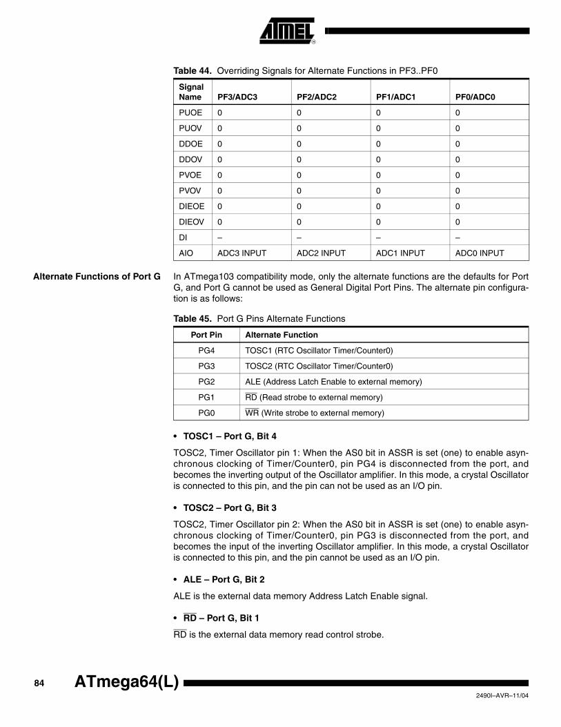
Alternate Functions of Port G In ATmega103 compatibility mode, only the alternate functions are the defaults for PortG, and Port G cannot be used as General Digital Port Pins. The alternate pin configura-tion is as follows:
• TOSC1 – Port G, Bit 4
TOSC2, Timer Oscillator pin 1: When the AS0 bit in ASSR is set (one) to enable asyn-chronous clocking of Timer/Counter0, pin PG4 is disconnected from the port, andbecomes the inverting output of the Oscillator amplifier. In this mode, a crystal Oscillatoris connected to this pin, and the pin can not be used as an I/O pin.
• TOSC2 – Port G, Bit 3
TOSC2, Timer Oscillator pin 2: When the AS0 bit in ASSR is set (one) to enable asyn-chronous clocking of Timer/Counter0, pin PG3 is disconnected from the port, andbecomes the input of the inverting Oscillator amplifier. In this mode, a crystal Oscillatoris connected to this pin, and the pin cannot be used as an I/O pin.
• ALE – Port G, Bit 2
ALE is the external data memory Address Latch Enable signal.
• RD – Port G, Bit 1
RD is the external data memory read control strobe.
Table 44. Overriding Signals for Alternate Functions in PF3..PF0
Signal Name PF3/ADC3 PF2/ADC2 PF1/ADC1 PF0/ADC0
PUOE 0 0 0 0
PUOV 0 0 0 0
DDOE 0 0 0 0
DDOV 0 0 0 0
PVOE 0 0 0 0
PVOV 0 0 0 0
DIEOE 0 0 0 0
DIEOV 0 0 0 0
DI – – – –
AIO ADC3 INPUT ADC2 INPUT ADC1 INPUT ADC0 INPUT
Table 45. Port G Pins Alternate Functions
Port Pin Alternate Function
PG4 TOSC1 (RTC Oscillator Timer/Counter0)
PG3 TOSC2 (RTC Oscillator Timer/Counter0)
PG2 ALE (Address Latch Enable to external memory)
PG1 RD (Read strobe to external memory)
PG0 WR (Write strobe to external memory)
84 ATmega64(L)2490I–AVR–11/04
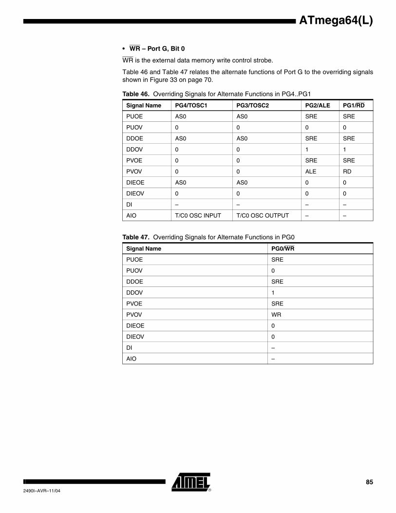
ATmega64(L)
• WR – Port G, Bit 0
WR is the external data memory write control strobe.
Table 46 and Table 47 relates the alternate functions of Port G to the overriding signalsshown in Figure 33 on page 70.
Table 46. Overriding Signals for Alternate Functions in PG4..PG1
Signal Name PG4/TOSC1 PG3/TOSC2 PG2/ALE PG1/RD
PUOE AS0 AS0 SRE SRE
PUOV 0 0 0 0
DDOE AS0 AS0 SRE SRE
DDOV 0 0 1 1
PVOE 0 0 SRE SRE
PVOV 0 0 ALE RD
DIEOE AS0 AS0 0 0
DIEOV 0 0 0 0
DI – – – –
AIO T/C0 OSC INPUT T/C0 OSC OUTPUT – –
Table 47. Overriding Signals for Alternate Functions in PG0
Signal Name PG0/WR
PUOE SRE
PUOV 0
DDOE SRE
DDOV 1
PVOE SRE
PVOV WR
DIEOE 0
DIEOV 0
DI –
AIO –
852490I–AVR–11/04
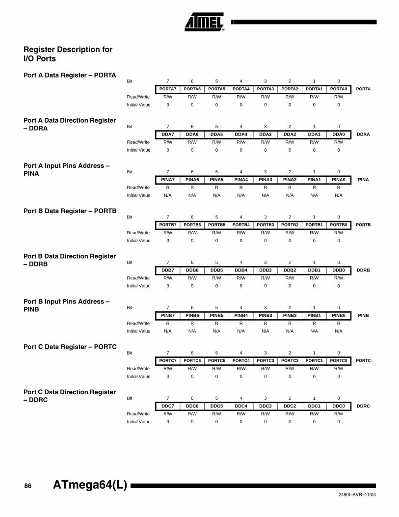
Register Description for I/O Ports
Port A Data Register – PORTA
Port A Data Direction Register – DDRA
Port A Input Pins Address – PINA
Port B Data Register – PORTB
Port B Data Direction Register – DDRB
Port B Input Pins Address – PINB
Port C Data Register – PORTC
Port C Data Direction Register – DDRC
Bit 7 6 5 4 3 2 1 0
PORTA7 PORTA6 PORTA5 PORTA4 PORTA3 PORTA2 PORTA1 PORTA0 PORTA
Read/Write R/W R/W R/W R/W R/W R/W R/W R/W
Initial Value 0 0 0 0 0 0 0 0
Bit 7 6 5 4 3 2 1 0
DDA7 DDA6 DDA5 DDA4 DDA3 DDA2 DDA1 DDA0 DDRARead/Write R/W R/W R/W R/W R/W R/W R/W R/W
Initial Value 0 0 0 0 0 0 0 0
Bit 7 6 5 4 3 2 1 0
PINA7 PINA6 PINA5 PINA4 PINA3 PINA2 PINA1 PINA0 PINARead/Write R R R R R R R R
Initial Value N/A N/A N/A N/A N/A N/A N/A N/A
Bit 7 6 5 4 3 2 1 0
PORTB7 PORTB6 PORTB5 PORTB4 PORTB3 PORTB2 PORTB1 PORTB0 PORTB
Read/Write R/W R/W R/W R/W R/W R/W R/W R/W
Initial Value 0 0 0 0 0 0 0 0
Bit 7 6 5 4 3 2 1 0
DDB7 DDB6 DDB5 DDB4 DDB3 DDB2 DDB1 DDB0 DDRBRead/Write R/W R/W R/W R/W R/W R/W R/W R/W
Initial Value 0 0 0 0 0 0 0 0
Bit 7 6 5 4 3 2 1 0
PINB7 PINB6 PINB5 PINB4 PINB3 PINB2 PINB1 PINB0 PINB
Read/Write R R R R R R R R
Initial Value N/A N/A N/A N/A N/A N/A N/A N/A
Bit 7 6 5 4 3 2 1 0
PORTC7 PORTC6 PORTC5 PORTC4 PORTC3 PORTC2 PORTC1 PORTC0 PORTC
Read/Write R/W R/W R/W R/W R/W R/W R/W R/W
Initial Value 0 0 0 0 0 0 0 0
Bit 7 6 5 4 3 2 1 0
DDC7 DDC6 DDC5 DDC4 DDC3 DDC2 DDC1 DDC0 DDRCRead/Write R/W R/W R/W R/W R/W R/W R/W R/W
Initial Value 0 0 0 0 0 0 0 0
86 ATmega64(L)2490I–AVR–11/04
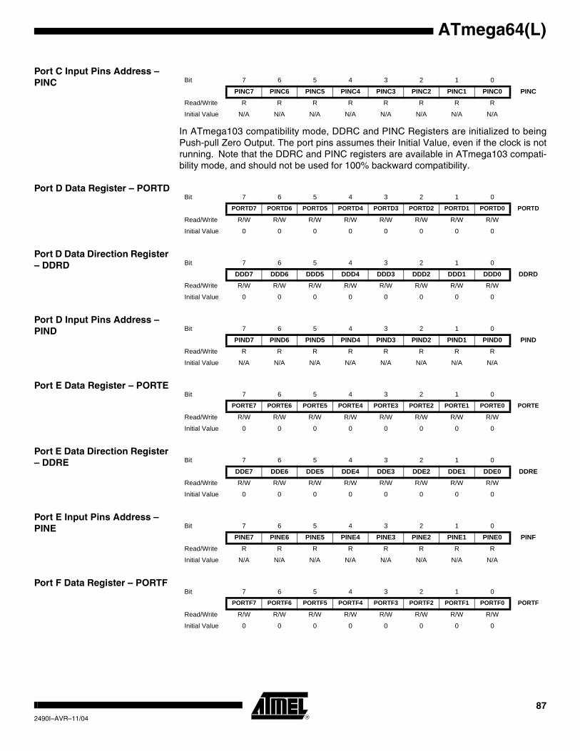
ATmega64(L)
Port C Input Pins Address – PINC
In ATmega103 compatibility mode, DDRC and PINC Registers are initialized to beingPush-pull Zero Output. The port pins assumes their Initial Value, even if the clock is notrunning. Note that the DDRC and PINC registers are available in ATmega103 compati-bility mode, and should not be used for 100% backward compatibility.
Port D Data Register – PORTD
Port D Data Direction Register – DDRD
Port D Input Pins Address – PIND
Port E Data Register – PORTE
Port E Data Direction Register – DDRE
Port E Input Pins Address – PINE
Port F Data Register – PORTF
Bit 7 6 5 4 3 2 1 0
PINC7 PINC6 PINC5 PINC4 PINC3 PINC2 PINC1 PINC0 PINCRead/Write R R R R R R R R
Initial Value N/A N/A N/A N/A N/A N/A N/A N/A
Bit 7 6 5 4 3 2 1 0
PORTD7 PORTD6 PORTD5 PORTD4 PORTD3 PORTD2 PORTD1 PORTD0 PORTD
Read/Write R/W R/W R/W R/W R/W R/W R/W R/W
Initial Value 0 0 0 0 0 0 0 0
Bit 7 6 5 4 3 2 1 0
DDD7 DDD6 DDD5 DDD4 DDD3 DDD2 DDD1 DDD0 DDRDRead/Write R/W R/W R/W R/W R/W R/W R/W R/W
Initial Value 0 0 0 0 0 0 0 0
Bit 7 6 5 4 3 2 1 0
PIND7 PIND6 PIND5 PIND4 PIND3 PIND2 PIND1 PIND0 PINDRead/Write R R R R R R R R
Initial Value N/A N/A N/A N/A N/A N/A N/A N/A
Bit 7 6 5 4 3 2 1 0
PORTE7 PORTE6 PORTE5 PORTE4 PORTE3 PORTE2 PORTE1 PORTE0 PORTE
Read/Write R/W R/W R/W R/W R/W R/W R/W R/W
Initial Value 0 0 0 0 0 0 0 0
Bit 7 6 5 4 3 2 1 0
DDE7 DDE6 DDE5 DDE4 DDE3 DDE2 DDE1 DDE0 DDRERead/Write R/W R/W R/W R/W R/W R/W R/W R/W
Initial Value 0 0 0 0 0 0 0 0
Bit 7 6 5 4 3 2 1 0
PINE7 PINE6 PINE5 PINE4 PINE3 PINE2 PINE1 PINE0 PINFRead/Write R R R R R R R R
Initial Value N/A N/A N/A N/A N/A N/A N/A N/A
Bit 7 6 5 4 3 2 1 0
PORTF7 PORTF6 PORTF5 PORTF4 PORTF3 PORTF2 PORTF1 PORTF0 PORTF
Read/Write R/W R/W R/W R/W R/W R/W R/W R/W
Initial Value 0 0 0 0 0 0 0 0
872490I–AVR–11/04
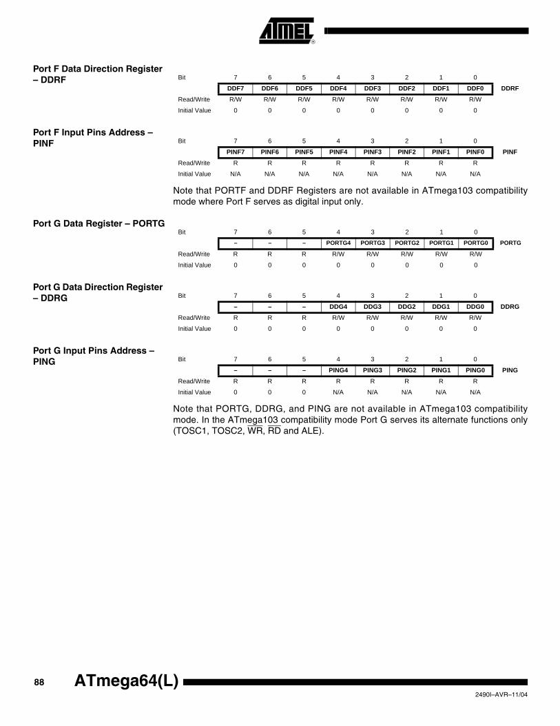
Port F Data Direction Register – DDRF
Port F Input Pins Address – PINF
Note that PORTF and DDRF Registers are not available in ATmega103 compatibilitymode where Port F serves as digital input only.
Port G Data Register – PORTG
Port G Data Direction Register – DDRG
Port G Input Pins Address – PING
Note that PORTG, DDRG, and PING are not available in ATmega103 compatibilitymode. In the ATmega103 compatibility mode Port G serves its alternate functions only(TOSC1, TOSC2, WR, RD and ALE).
Bit 7 6 5 4 3 2 1 0
DDF7 DDF6 DDF5 DDF4 DDF3 DDF2 DDF1 DDF0 DDRFRead/Write R/W R/W R/W R/W R/W R/W R/W R/W
Initial Value 0 0 0 0 0 0 0 0
Bit 7 6 5 4 3 2 1 0
PINF7 PINF6 PINF5 PINF4 PINF3 PINF2 PINF1 PINF0 PINFRead/Write R R R R R R R R
Initial Value N/A N/A N/A N/A N/A N/A N/A N/A
Bit 7 6 5 4 3 2 1 0
– – – PORTG4 PORTG3 PORTG2 PORTG1 PORTG0 PORTG
Read/Write R R R R/W R/W R/W R/W R/W
Initial Value 0 0 0 0 0 0 0 0
Bit 7 6 5 4 3 2 1 0
– – – DDG4 DDG3 DDG2 DDG1 DDG0 DDRGRead/Write R R R R/W R/W R/W R/W R/W
Initial Value 0 0 0 0 0 0 0 0
Bit 7 6 5 4 3 2 1 0
– – – PING4 PING3 PING2 PING1 PING0 PINGRead/Write R R R R R R R R
Initial Value 0 0 0 N/A N/A N/A N/A N/A
88 ATmega64(L)2490I–AVR–11/04
ATmega64(L)
External Interrupts The External Interrupts are triggered by the INT7:0 pins. Observe that, if enabled, theinterrupts will trigger even if the INT7:0 pins are configured as outputs. This feature pro-vides a way of generating a software interrupt. The external interrupts can be triggeredby a falling or rising edge or a low level. This is set up as indicated in the specification forthe External Interrupt Control Registers – EICRA (INT3:0) and EICRB (INT7:4). Whenthe External Interrupt is enabled and is configured as level triggered, the interrupt willtrigger as long as the pin is held low. Note that recognition of falling or rising edge inter-rupts on INT7:4 requires the presence of an I/O clock, described in “Clock Systems andtheir Distribution” on page 35. Low level interrupts and the edge interrupt on INT3:0 aredetected asynchronously. This implies that these interrupts can be used for waking thepart also from sleep modes other than Idle mode. The I/O clock is halted in all sleepmodes except Idle mode.
Note that if a level triggered interrupt is used for wake-up from Power-down mode, thechanged level must be held for some time to wake up the MCU. This makes the MCUless sensitive to noise. The changed level is sampled twice by the Watchdog Oscillatorclock. The period of the Watchdog Oscillator is 1 µs (nominal) at 5.0V and 25°C. Thefrequency of the Watchdog Oscillator is voltage dependent as shown in the “ElectricalCharacteristics” on page 327. The MCU will wake up if the input has the required levelduring this sampling or if it is held until the end of the start-up time. The start-up time isdefined by the SUT Fuses as described in “Clock Systems and their Distribution” onpage 35. If the level is sampled twice by the Watchdog Oscillator clock but disappearsbefore the end of the start-up time, the MCU will still wake up, but no interrupt will begenerated. The required level must be held long enough for the MCU to complete thewake up to trigger the level interrupt.
External Interrupt Control Register A – EICRA
This Register can not be reached in ATmega103 compatibility mode, but the InitialValue defines INT3:0 as low level interrupts, as in ATmega103.
• Bits 7..0 – ISC31, ISC30 - ISC00, ISC00: External Interrupt 3 - 0 Sense Control Bits
The External Interrupts 3 - 0 are activated by the external pins INT3:0 if the SREG I-flagand the corresponding interrupt mask in the EIMSK is set. The level and edges on theexternal pins that activate the interrupts are defined in Table 48. Edges on INT3..INT0are registered asynchronously. Pulses on INT3:0 pins wider than the minimum pulsewidth given in Table 49 will generate an interrupt. Shorter pulses are not guaranteed togenerate an interrupt. If low level interrupt is selected, the low level must be held untilthe completion of the currently executing instruction to generate an interrupt. If enabled,a level triggered interrupt will generate an interrupt request as long as the pin is heldlow. When changing the ISCn bit, an interrupt can occur. Therefore, it is recommendedto first disable INTn by clearing its Interrupt Enable bit in the EIMSK Register. Then, theISCn bit can be changed. Finally, the INTn interrupt flag should be cleared by writing alogical one to its Interrupt Flag bit (INTFn) in the EIFR Register before the interrupt is re-enabled.
Bit 7 6 5 4 3 2 1 0
ISC31 ISC30 ISC21 ISC20 ISC11 ISC10 ISC01 ISC00 EICRARead/Write R/W R/W R/W R/W R/W R/W R/W R/W
Initial Value 0 0 0 0 0 0 0 0
892490I–AVR–11/04
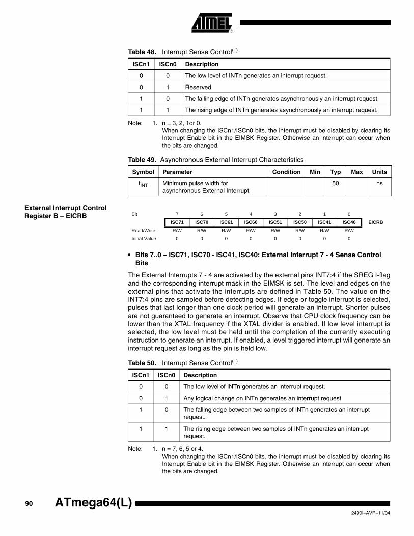
Note: 1. n = 3, 2, 1or 0.When changing the ISCn1/ISCn0 bits, the interrupt must be disabled by clearing itsInterrupt Enable bit in the EIMSK Register. Otherwise an interrupt can occur whenthe bits are changed.
External Interrupt Control Register B – EICRB
• Bits 7..0 – ISC71, ISC70 - ISC41, ISC40: External Interrupt 7 - 4 Sense Control Bits
The External Interrupts 7 - 4 are activated by the external pins INT7:4 if the SREG I-flagand the corresponding interrupt mask in the EIMSK is set. The level and edges on theexternal pins that activate the interrupts are defined in Table 50. The value on theINT7:4 pins are sampled before detecting edges. If edge or toggle interrupt is selected,pulses that last longer than one clock period will generate an interrupt. Shorter pulsesare not guaranteed to generate an interrupt. Observe that CPU clock frequency can belower than the XTAL frequency if the XTAL divider is enabled. If low level interrupt isselected, the low level must be held until the completion of the currently executinginstruction to generate an interrupt. If enabled, a level triggered interrupt will generate aninterrupt request as long as the pin is held low.
Note: 1. n = 7, 6, 5 or 4.When changing the ISCn1/ISCn0 bits, the interrupt must be disabled by clearing itsInterrupt Enable bit in the EIMSK Register. Otherwise an interrupt can occur whenthe bits are changed.
Table 48. Interrupt Sense Control(1)
ISCn1 ISCn0 Description
0 0 The low level of INTn generates an interrupt request.
0 1 Reserved
1 0 The falling edge of INTn generates asynchronously an interrupt request.
1 1 The rising edge of INTn generates asynchronously an interrupt request.
Table 49. Asynchronous External Interrupt Characteristics
Symbol Parameter Condition Min Typ Max Units
tINT Minimum pulse width for asynchronous External Interrupt
50 ns
Bit 7 6 5 4 3 2 1 0
ISC71 ISC70 ISC61 ISC60 ISC51 ISC50 ISC41 ISC40 EICRBRead/Write R/W R/W R/W R/W R/W R/W R/W R/W
Initial Value 0 0 0 0 0 0 0 0
Table 50. Interrupt Sense Control(1)
ISCn1 ISCn0 Description
0 0 The low level of INTn generates an interrupt request.
0 1 Any logical change on INTn generates an interrupt request
1 0 The falling edge between two samples of INTn generates an interrupt request.
1 1 The rising edge between two samples of INTn generates an interrupt request.
90 ATmega64(L)2490I–AVR–11/04
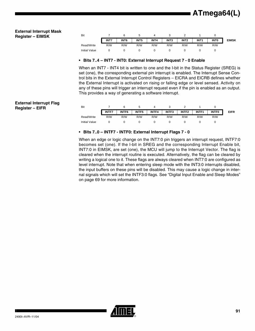
ATmega64(L)
External Interrupt Mask Register – EIMSK
• Bits 7..4 – INT7 - INT0: External Interrupt Request 7 - 0 Enable
When an INT7 - INT4 bit is written to one and the I-bit in the Status Register (SREG) isset (one), the corresponding external pin interrupt is enabled. The Interrupt Sense Con-trol bits in the External Interrupt Control Registers – EICRA and EICRB defines whetherthe External Interrupt is activated on rising or falling edge or level sensed. Activity onany of these pins will trigger an interrupt request even if the pin is enabled as an output.This provides a way of generating a software interrupt.
External Interrupt Flag Register – EIFR
• Bits 7..0 – INTF7 - INTF0: External Interrupt Flags 7 - 0
When an edge or logic change on the INT7:0 pin triggers an interrupt request, INTF7:0becomes set (one). If the I-bit in SREG and the corresponding Interrupt Enable bit,INT7:0 in EIMSK, are set (one), the MCU will jump to the Interrupt Vector. The flag iscleared when the interrupt routine is executed. Alternatively, the flag can be cleared bywriting a logical one to it. These flags are always cleared when INT7:0 are configured aslevel interrupt. Note that when entering sleep mode with the INT3:0 interrupts disabled,the input buffers on these pins will be disabled. This may cause a logic change in inter-nal signals which will set the INTF3:0 flags. See “Digital Input Enable and Sleep Modes”on page 69 for more information.
Bit 7 6 5 4 3 2 1 0
INT7 INT6 INT5 INT4 INT3 INT2 INT1 INT0 EIMSKRead/Write R/W R/W R/W R/W R/W R/W R/W R/W
Initial Value 0 0 0 0 0 0 0 0
Bit 7 6 5 4 3 2 1 0
INTF7 INTF6 INTF5 INTF4 INTF3 INTF2 INTF1 INTF0 EIFRRead/Write R/W R/W R/W R/W R/W R/W R/W R/W
Initial Value 0 0 0 0 0 0 0 0
912490I–AVR–11/04
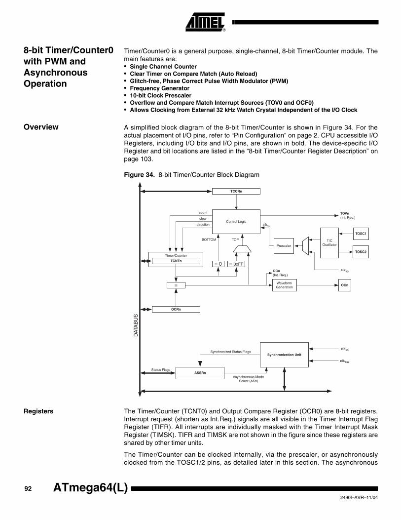
8-bit Timer/Counter0 with PWM and Asynchronous Operation
Timer/Counter0 is a general purpose, single-channel, 8-bit Timer/Counter module. Themain features are:• Single Channel Counter• Clear Timer on Compare Match (Auto Reload)• Glitch-free, Phase Correct Pulse Width Modulator (PWM)• Frequency Generator• 10-bit Clock Prescaler• Overflow and Compare Match Interrupt Sources (TOV0 and OCF0)• Allows Clocking from External 32 kHz Watch Crystal Independent of the I/O Clock
Overview A simplified block diagram of the 8-bit Timer/Counter is shown in Figure 34. For theactual placement of I/O pins, refer to “Pin Configuration” on page 2. CPU accessible I/ORegisters, including I/O bits and I/O pins, are shown in bold. The device-specific I/ORegister and bit locations are listed in the “8-bit Timer/Counter Register Description” onpage 103.
Figure 34. 8-bit Timer/Counter Block Diagram
Registers The Timer/Counter (TCNT0) and Output Compare Register (OCR0) are 8-bit registers.Interrupt request (shorten as Int.Req.) signals are all visible in the Timer Interrupt FlagRegister (TIFR). All interrupts are individually masked with the Timer Interrupt MaskRegister (TIMSK). TIFR and TIMSK are not shown in the figure since these registers areshared by other timer units.
The Timer/Counter can be clocked internally, via the prescaler, or asynchronouslyclocked from the TOSC1/2 pins, as detailed later in this section. The asynchronous
Timer/Counter
DAT
AB
US
=
TCNTn
WaveformGeneration
OCn
= 0
Control Logic
= 0xFF
TOPBOTTOM
count
clear
direction
TOVn(Int. Req.)
OCn(Int. Req.)
Synchronization Unit
OCRn
TCCRn
ASSRnStatus Flags
clkI/O
clkASY
Synchronized Status Flags
Asynchronous ModeSelect (ASn)
TOSC1
T/COscillator
TOSC2
Prescaler
clkTn
clkI/O
92 ATmega64(L)2490I–AVR–11/04
ATmega64(L)
operation is controlled by the Asynchronous Status Register (ASSR). The Clock Selectlogic block controls which clock source the Timer/Counter uses to increment (or decre-ment) its value. The Timer/Counter is inactive when no clock source is selected. Theoutput from the Clock Select logic is referred to as the timer clock (clkT0).
The double buffered Output Compare Register (OCR0) is compared with theTimer/Counter value at all times. The result of the compare can be used by the Wave-form Generator to generate a PWM or variable frequency output on the Output Comparepin (OC0). See “Output Compare Unit” on page 94. for details. The Compare Matchevent will also set the Compare Flag (OCF0) which can be used to generate an OutputCompare interrupt request.
Definitions Many register and bit references in this datasheet are written in general form. A lowercase “n” replaces the Timer/Counter number, in this case 0. However, when using theregister or bit defines in a program, the precise form must be used i.e. TCNT0 foraccessing Timer/Counter0 counter value and so on.
The definitions in Table 51 are also used extensively throughout this section.
Timer/Counter Clock Sources
The Timer/Counter can be clocked by an internal synchronous or an external asynchro-nous clock source. The clock source clkT0 is by default equal to the MCU clock, clkI/O.When the AS0 bit in the ASSR Register is written to logic one, the clock source is takenfrom the Timer/Counter Oscillator connected to TOSC1 and TOSC2. For details onasynchronous operation, see “Asynchronous Status Register – ASSR” on page 106. Fordetails on clock sources and prescaler, see “Timer/Counter Prescaler” on page 109.
Table 51. Definitions
BOTTOM The counter reaches the BOTTOM when it becomes zero (0x00).
MAX The counter reaches its MAXimum when it becomes 0xFF (decimal 255).
TOP The counter reaches the TOP when it becomes equal to the highestvalue in the count sequence. The TOP value can be assigned to be thefixed value 0xFF (MAX) or the value stored in the OCR0 Register. Theassignment is dependent on the mode of operation.
932490I–AVR–11/04
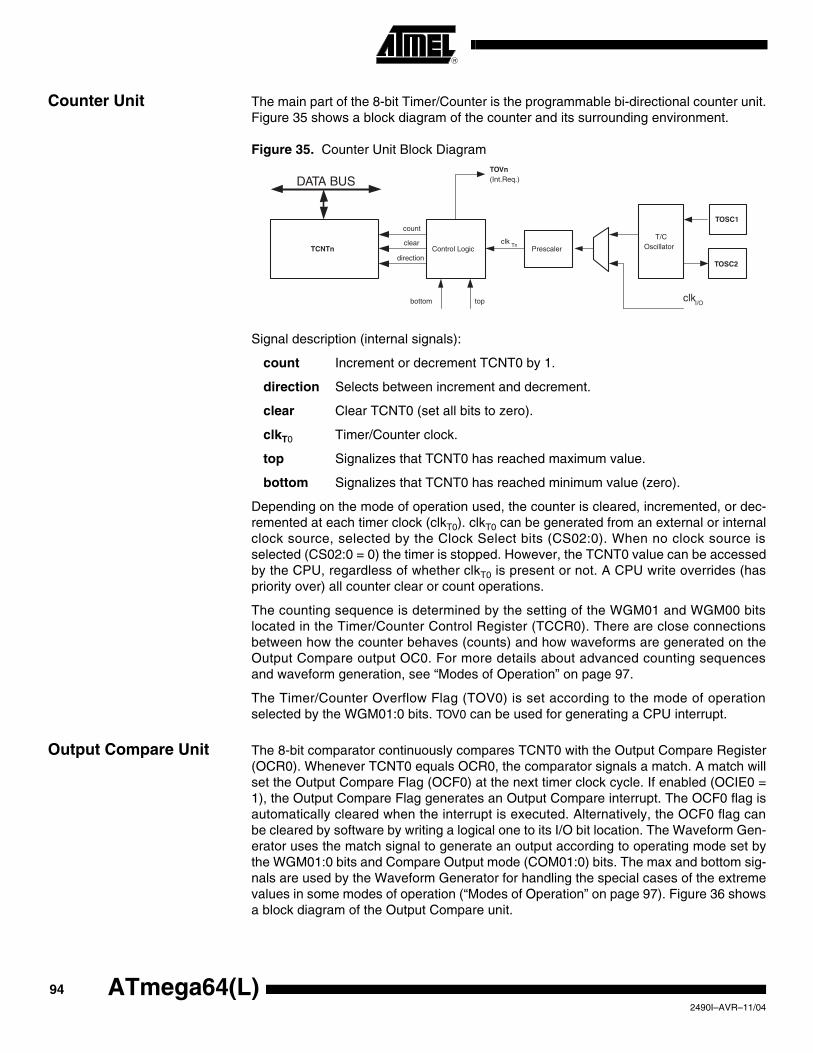
Counter Unit The main part of the 8-bit Timer/Counter is the programmable bi-directional counter unit.Figure 35 shows a block diagram of the counter and its surrounding environment.
Figure 35. Counter Unit Block Diagram
Signal description (internal signals):
count Increment or decrement TCNT0 by 1.
direction Selects between increment and decrement.
clear Clear TCNT0 (set all bits to zero).
clkT0 Timer/Counter clock.
top Signalizes that TCNT0 has reached maximum value.
bottom Signalizes that TCNT0 has reached minimum value (zero).
Depending on the mode of operation used, the counter is cleared, incremented, or dec-remented at each timer clock (clkT0). clkT0 can be generated from an external or internalclock source, selected by the Clock Select bits (CS02:0). When no clock source isselected (CS02:0 = 0) the timer is stopped. However, the TCNT0 value can be accessedby the CPU, regardless of whether clkT0 is present or not. A CPU write overrides (haspriority over) all counter clear or count operations.
The counting sequence is determined by the setting of the WGM01 and WGM00 bitslocated in the Timer/Counter Control Register (TCCR0). There are close connectionsbetween how the counter behaves (counts) and how waveforms are generated on theOutput Compare output OC0. For more details about advanced counting sequencesand waveform generation, see “Modes of Operation” on page 97.
The Timer/Counter Overflow Flag (TOV0) is set according to the mode of operationselected by the WGM01:0 bits. TOV0 can be used for generating a CPU interrupt.
Output Compare Unit The 8-bit comparator continuously compares TCNT0 with the Output Compare Register(OCR0). Whenever TCNT0 equals OCR0, the comparator signals a match. A match willset the Output Compare Flag (OCF0) at the next timer clock cycle. If enabled (OCIE0 =1), the Output Compare Flag generates an Output Compare interrupt. The OCF0 flag isautomatically cleared when the interrupt is executed. Alternatively, the OCF0 flag canbe cleared by software by writing a logical one to its I/O bit location. The Waveform Gen-erator uses the match signal to generate an output according to operating mode set bythe WGM01:0 bits and Compare Output mode (COM01:0) bits. The max and bottom sig-nals are used by the Waveform Generator for handling the special cases of the extremevalues in some modes of operation (“Modes of Operation” on page 97). Figure 36 showsa block diagram of the Output Compare unit.
DATA BUS
TCNTn Control Logic
count
TOVn(Int.Req.)
topbottom
direction
clear
TOSC1
T/COscillator
TOSC2
Prescaler
clkI/O
clkTn
94 ATmega64(L)2490I–AVR–11/04
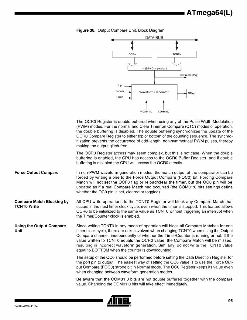
ATmega64(L)
Figure 36. Output Compare Unit, Block Diagram
The OCR0 Register is double buffered when using any of the Pulse Width Modulation(PWM) modes. For the normal and Clear Timer on Compare (CTC) modes of operation,the double buffering is disabled. The double buffering synchronizes the update of theOCR0 Compare Register to either top or bottom of the counting sequence. The synchro-nization prevents the occurrence of odd-length, non-symmetrical PWM pulses, therebymaking the output glitch-free.
The OCR0 Register access may seem complex, but this is not case. When the doublebuffering is enabled, the CPU has access to the OCR0 Buffer Register, and if doublebuffering is disabled the CPU will access the OCR0 directly.
Force Output Compare In non-PWM waveform generation modes, the match output of the comparator can beforced by writing a one to the Force Output Compare (FOC0) bit. Forcing CompareMatch will not set the OCF0 flag or reload/clear the timer, but the OC0 pin will beupdated as if a real Compare Match had occurred (the COM01:0 bits settings definewhether the OC0 pin is set, cleared or toggled).
Compare Match Blocking by TCNT0 Write
All CPU write operations to the TCNT0 Register will block any Compare Match thatoccurs in the next timer clock cycle, even when the timer is stopped. This feature allowsOCR0 to be initialized to the same value as TCNT0 without triggering an interrupt whenthe Timer/Counter clock is enabled.
Using the Output Compare Unit
Since writing TCNT0 in any mode of operation will block all Compare Matches for onetimer clock cycle, there are risks involved when changing TCNT0 when using the OutputCompare channel, independently of whether the Timer/Counter is running or not. If thevalue written to TCNT0 equals the OCR0 value, the Compare Match will be missed,resulting in incorrect waveform generation. Similarly, do not write the TCNT0 valueequal to BOTTOM when the counter is downcounting.
The setup of the OC0 should be performed before setting the Data Direction Register forthe port pin to output. The easiest way of setting the OC0 value is to use the Force Out-put Compare (FOC0) strobe bit in Normal mode. The OC0 Register keeps its value evenwhen changing between waveform generation modes.
Be aware that the COM01:0 bits are not double buffered together with the comparevalue. Changing the COM01:0 bits will take effect immediately.
OCFn (Int.Req.)
= (8-bit Comparator )
OCRn
OCxy
DATA BUS
TCNTn
WGMn1:0
Waveform Generator
top
FOCn
COMn1:0
bottom
952490I–AVR–11/04
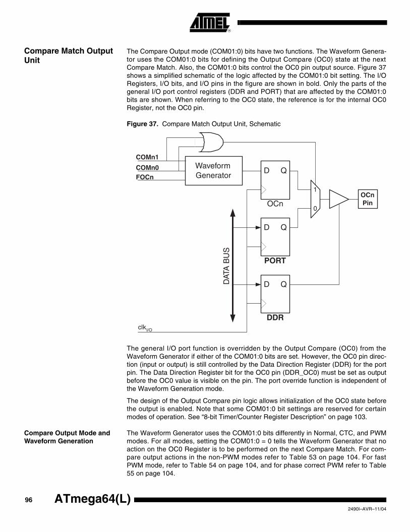
Compare Match Output Unit
The Compare Output mode (COM01:0) bits have two functions. The Waveform Genera-tor uses the COM01:0 bits for defining the Output Compare (OC0) state at the nextCompare Match. Also, the COM01:0 bits control the OC0 pin output source. Figure 37shows a simplified schematic of the logic affected by the COM01:0 bit setting. The I/ORegisters, I/O bits, and I/O pins in the figure are shown in bold. Only the parts of thegeneral I/O port control registers (DDR and PORT) that are affected by the COM01:0bits are shown. When referring to the OC0 state, the reference is for the internal OC0Register, not the OC0 pin.
Figure 37. Compare Match Output Unit, Schematic
The general I/O port function is overridden by the Output Compare (OC0) from theWaveform Generator if either of the COM01:0 bits are set. However, the OC0 pin direc-tion (input or output) is still controlled by the Data Direction Register (DDR) for the portpin. The Data Direction Register bit for the OC0 pin (DDR_OC0) must be set as outputbefore the OC0 value is visible on the pin. The port override function is independent ofthe Waveform Generation mode.
The design of the Output Compare pin logic allows initialization of the OC0 state beforethe output is enabled. Note that some COM01:0 bit settings are reserved for certainmodes of operation. See “8-bit Timer/Counter Register Description” on page 103.
Compare Output Mode and Waveform Generation
The Waveform Generator uses the COM01:0 bits differently in Normal, CTC, and PWMmodes. For all modes, setting the COM01:0 = 0 tells the Waveform Generator that noaction on the OC0 Register is to be performed on the next Compare Match. For com-pare output actions in the non-PWM modes refer to Table 53 on page 104. For fastPWM mode, refer to Table 54 on page 104, and for phase correct PWM refer to Table55 on page 104.
PORT
DDR
D Q
D Q
OCnPinOCn
D QWaveformGenerator
COMn1
COMn0
0
1
DAT
A B
US
FOCn
clkI/O
96 ATmega64(L)2490I–AVR–11/04
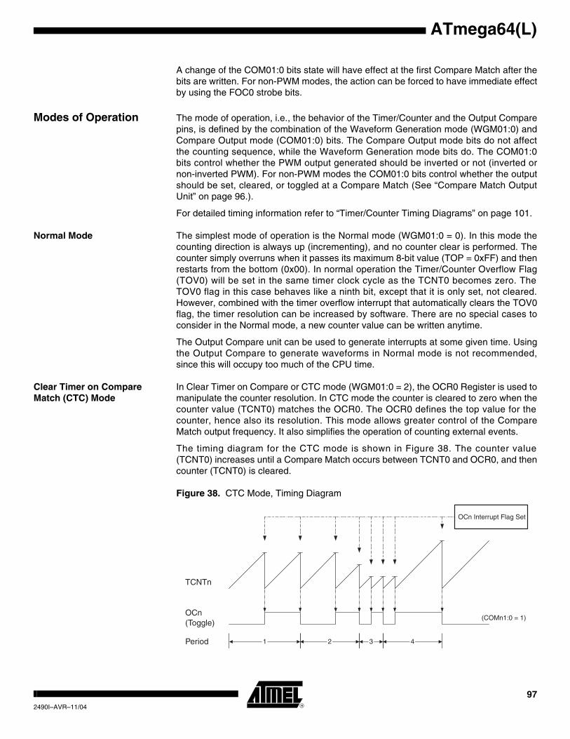
ATmega64(L)
A change of the COM01:0 bits state will have effect at the first Compare Match after thebits are written. For non-PWM modes, the action can be forced to have immediate effectby using the FOC0 strobe bits.
Modes of Operation The mode of operation, i.e., the behavior of the Timer/Counter and the Output Comparepins, is defined by the combination of the Waveform Generation mode (WGM01:0) andCompare Output mode (COM01:0) bits. The Compare Output mode bits do not affectthe counting sequence, while the Waveform Generation mode bits do. The COM01:0bits control whether the PWM output generated should be inverted or not (inverted ornon-inverted PWM). For non-PWM modes the COM01:0 bits control whether the outputshould be set, cleared, or toggled at a Compare Match (See “Compare Match OutputUnit” on page 96.).
For detailed timing information refer to “Timer/Counter Timing Diagrams” on page 101.
Normal Mode The simplest mode of operation is the Normal mode (WGM01:0 = 0). In this mode thecounting direction is always up (incrementing), and no counter clear is performed. Thecounter simply overruns when it passes its maximum 8-bit value (TOP = 0xFF) and thenrestarts from the bottom (0x00). In normal operation the Timer/Counter Overflow Flag(TOV0) will be set in the same timer clock cycle as the TCNT0 becomes zero. TheTOV0 flag in this case behaves like a ninth bit, except that it is only set, not cleared.However, combined with the timer overflow interrupt that automatically clears the TOV0flag, the timer resolution can be increased by software. There are no special cases toconsider in the Normal mode, a new counter value can be written anytime.
The Output Compare unit can be used to generate interrupts at some given time. Usingthe Output Compare to generate waveforms in Normal mode is not recommended,since this will occupy too much of the CPU time.
Clear Timer on Compare Match (CTC) Mode
In Clear Timer on Compare or CTC mode (WGM01:0 = 2), the OCR0 Register is used tomanipulate the counter resolution. In CTC mode the counter is cleared to zero when thecounter value (TCNT0) matches the OCR0. The OCR0 defines the top value for thecounter, hence also its resolution. This mode allows greater control of the CompareMatch output frequency. It also simplifies the operation of counting external events.
The timing diagram for the CTC mode is shown in Figure 38. The counter value(TCNT0) increases until a Compare Match occurs between TCNT0 and OCR0, and thencounter (TCNT0) is cleared.
Figure 38. CTC Mode, Timing Diagram
TCNTn
OCn(Toggle)
OCn Interrupt Flag Set
1 4Period 2 3
(COMn1:0 = 1)
972490I–AVR–11/04
An interrupt can be generated each time the counter value reaches the TOP value byusing the OCF0 flag. If the interrupt is enabled, the interrupt handler routine can be usedfor updating the TOP value. However, changing the TOP to a value close to BOTTOMwhen the counter is running with none or a low prescaler value must be done with caresince the CTC mode does not have the double buffering feature. If the new value writtento OCR0 is lower than the current value of TCNT0, the counter will miss the CompareMatch. The counter will then have to count to its maximum value (0xFF) and wraparound starting at 0x00 before the Compare Match can occur.
For generating a waveform output in CTC mode, the OC0 output can be set to toggle itslogical level on each Compare Match by setting the Compare Output mode bits to togglemode (COM01:0 = 1). The OC0 value will not be visible on the port pin unless the datadirection for the pin is set to output. The waveform generated will have a maximum fre-quency of fOC0 = fclk_I/O/2 when OCR0 is set to zero (0x00). The waveform frequency isdefined by the following equation:
The N variable represents the prescale factor (1, 8, 32, 64, 128, 256, or 1024).
As for the Normal mode of operation, the TOV0 flag is set in the same timer clock cyclethat the counter counts from MAX to 0x00.
Fast PWM Mode The fast Pulse Width Modulation or fast PWM mode (WGM01:0 = 3) provides a high fre-quency PWM waveform generation option. The fast PWM differs from the other PWMoption by its single-slope operation. The counter counts from BOTTOM to MAX thenrestarts from BOTTOM. In non-inverting Compare Output mode, the Output Compare(OC0) is cleared on the Compare Match between TCNT0 and OCR0, and set at BOT-TOM. In inverting Compare Output mode, the output is set on Compare Match andcleared at BOTTOM. Due to the single-slope operation, the operating frequency of thefast PWM mode can be twice as high as the phase correct PWM mode that uses dual-slope operation. This high frequency makes the fast PWM mode well suited for powerregulation, rectification, and DAC applications. High frequency allows physically smallsized external components (coils, capacitors), and therefore reduces total system cost.
In fast PWM mode, the counter is incremented until the counter value matches the MAXvalue. The counter is then cleared at the following timer clock cycle. The timing diagramfor the fast PWM mode is shown in Figure 39. The TCNT0 value is in the timing diagramshown as a histogram for illustrating the single-slope operation. The diagram includesnon-inverted and inverted PWM outputs. The small horizontal line marks on the TCNT0slopes represent Compare Matches between OCR0 and TCNT0.
fOCnfclk_I/O
2 N 1 OCRn+( )⋅ ⋅-----------------------------------------------=
98 ATmega64(L)2490I–AVR–11/04
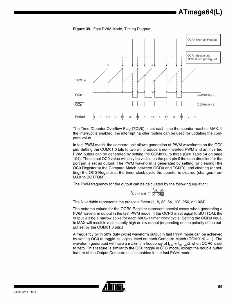
ATmega64(L)
Figure 39. Fast PWM Mode, Timing Diagram
The Timer/Counter Overflow Flag (TOV0) is set each time the counter reaches MAX. Ifthe interrupt is enabled, the interrupt handler routine can be used for updating the com-pare value.
In fast PWM mode, the compare unit allows generation of PWM waveforms on the OC0pin. Setting the COM01:0 bits to two will produce a non-inverted PWM and an invertedPWM output can be generated by setting the COM01:0 to three (See Table 54 on page104). The actual OC0 value will only be visible on the port pin if the data direction for theport pin is set as output. The PWM waveform is generated by setting (or clearing) theOC0 Register at the Compare Match between OCR0 and TCNT0, and clearing (or set-ting) the OC0 Register at the timer clock cycle the counter is cleared (changes fromMAX to BOTTOM).
The PWM frequency for the output can be calculated by the following equation:
The N variable represents the prescale factor (1, 8, 32, 64, 128, 256, or 1024).
The extreme values for the OCR0 Register represent special cases when generating aPWM waveform output in the fast PWM mode. If the OCR0 is set equal to BOTTOM, theoutput will be a narrow spike for each MAX+1 timer clock cycle. Setting the OCR0 equalto MAX will result in a constantly high or low output (depending on the polarity of the out-put set by the COM01:0 bits.)
A frequency (with 50% duty cycle) waveform output in fast PWM mode can be achievedby setting OC0 to toggle its logical level on each Compare Match (COM01:0 = 1). Thewaveform generated will have a maximum frequency of foc0 = fclk_I/O/2 when OCR0 is setto zero. This feature is similar to the OC0 toggle in CTC mode, except the double bufferfeature of the Output Compare unit is enabled in the fast PWM mode.
TCNTn
OCRn Update andTOVn Interrupt Flag Set
1Period 2 3
OCn
OCn
(COMn1:0 = 2)
(COMn1:0 = 3)
OCRn Interrupt Flag Set
4 5 6 7
fOCnPWMfclk_I/O
N 256⋅------------------=
992490I–AVR–11/04
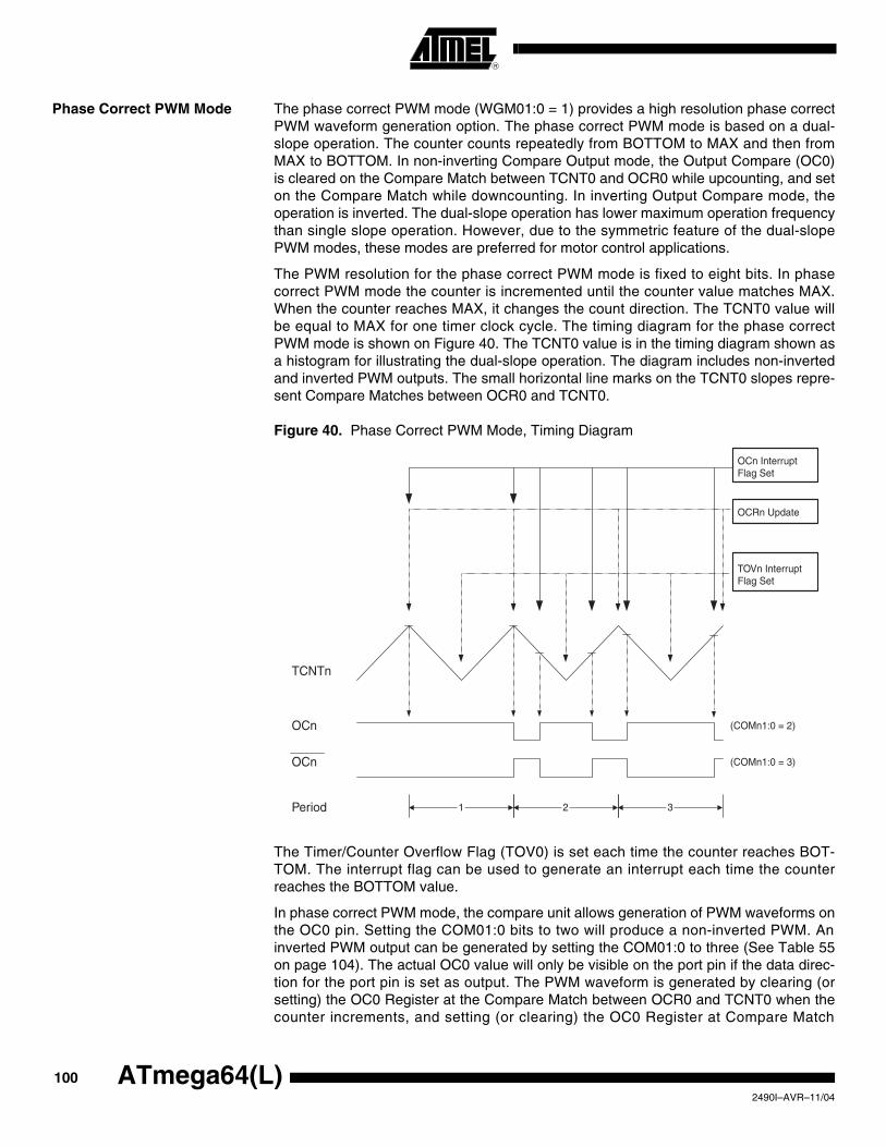
Phase Correct PWM Mode The phase correct PWM mode (WGM01:0 = 1) provides a high resolution phase correctPWM waveform generation option. The phase correct PWM mode is based on a dual-slope operation. The counter counts repeatedly from BOTTOM to MAX and then fromMAX to BOTTOM. In non-inverting Compare Output mode, the Output Compare (OC0)is cleared on the Compare Match between TCNT0 and OCR0 while upcounting, and seton the Compare Match while downcounting. In inverting Output Compare mode, theoperation is inverted. The dual-slope operation has lower maximum operation frequencythan single slope operation. However, due to the symmetric feature of the dual-slopePWM modes, these modes are preferred for motor control applications.
The PWM resolution for the phase correct PWM mode is fixed to eight bits. In phasecorrect PWM mode the counter is incremented until the counter value matches MAX.When the counter reaches MAX, it changes the count direction. The TCNT0 value willbe equal to MAX for one timer clock cycle. The timing diagram for the phase correctPWM mode is shown on Figure 40. The TCNT0 value is in the timing diagram shown asa histogram for illustrating the dual-slope operation. The diagram includes non-invertedand inverted PWM outputs. The small horizontal line marks on the TCNT0 slopes repre-sent Compare Matches between OCR0 and TCNT0.
Figure 40. Phase Correct PWM Mode, Timing Diagram
The Timer/Counter Overflow Flag (TOV0) is set each time the counter reaches BOT-TOM. The interrupt flag can be used to generate an interrupt each time the counterreaches the BOTTOM value.
In phase correct PWM mode, the compare unit allows generation of PWM waveforms onthe OC0 pin. Setting the COM01:0 bits to two will produce a non-inverted PWM. Aninverted PWM output can be generated by setting the COM01:0 to three (See Table 55on page 104). The actual OC0 value will only be visible on the port pin if the data direc-tion for the port pin is set as output. The PWM waveform is generated by clearing (orsetting) the OC0 Register at the Compare Match between OCR0 and TCNT0 when thecounter increments, and setting (or clearing) the OC0 Register at Compare Match
TOVn Interrupt Flag Set
OCn Interrupt Flag Set
1 2 3
TCNTn
Period
OCn
OCn
(COMn1:0 = 2)
(COMn1:0 = 3)
OCRn Update
100 ATmega64(L)2490I–AVR–11/04
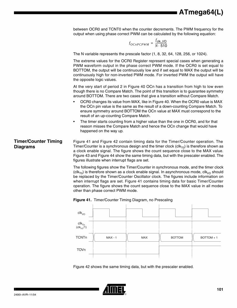
ATmega64(L)
between OCR0 and TCNT0 when the counter decrements. The PWM frequency for theoutput when using phase correct PWM can be calculated by the following equation:
The N variable represents the prescale factor (1, 8, 32, 64, 128, 256, or 1024).
The extreme values for the OCR0 Register represent special cases when generating aPWM waveform output in the phase correct PWM mode. If the OCR0 is set equal toBOTTOM, the output will be continuously low and if set equal to MAX the output will becontinuously high for non-inverted PWM mode. For inverted PWM the output will havethe opposite logic values.
At the very start of period 2 in Figure 40 OCn has a transition from high to low eventhough there is no Compare Match. The point of this transition is to guarantee symmetryaround BOTTOM. There are two cases that give a transition without Compare Match.
• OCR0 changes its value from MAX, like in Figure 40. When the OCR0 value is MAX the OCn pin value is the same as the result of a down-counting Compare Match. To ensure symmetry around BOTTOM the OCn value at MAX must correspond to the result of an up-counting Compare Match.
• The timer starts counting from a higher value than the one in OCR0, and for that reason misses the Compare Match and hence the OCn change that would have happened on the way up.
Timer/Counter Timing Diagrams
Figure 41 and Figure 42 contain timing data for the Timer/Counter operation. TheTimer/Counter is a synchronous design and the timer clock (clkT0) is therefore shown asa clock enable signal. The figure shows the count sequence close to the MAX value.Figure 43 and Figure 44 show the same timing data, but with the prescaler enabled. Thefigures illustrate when interrupt flags are set.
The following figures show the Timer/Counter in synchronous mode, and the timer clock(clkT0) is therefore shown as a clock enable signal. In asynchronous mode, clkI/O shouldbe replaced by the Timer/Counter Oscillator clock. The figures include information onwhen interrupt flags are set. Figure 41 contains timing data for basic Timer/Counteroperation. The figure shows the count sequence close to the MAX value in all modesother than phase correct PWM mode.
Figure 41. Timer/Counter Timing Diagram, no Prescaling
Figure 42 shows the same timing data, but with the prescaler enabled.
fOCnPCPWMfclk_I/O
N 510⋅------------------=
clkTn(clkI/O/1)
TOVn
clkI/O
TCNTn MAX - 1 MAX BOTTOM BOTTOM + 1
1012490I–AVR–11/04
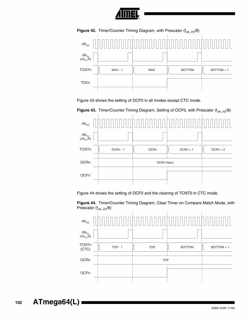
Figure 42. Timer/Counter Timing Diagram, with Prescaler (fclk_I/O/8)
Figure 43 shows the setting of OCF0 in all modes except CTC mode.
Figure 43. Timer/Counter Timing Diagram, Setting of OCF0, with Prescaler (fclk_I/O/8)
Figure 44 shows the setting of OCF0 and the clearing of TCNT0 in CTC mode.
Figure 44. Timer/Counter Timing Diagram, Clear Timer on Compare Match Mode, withPrescaler (fclk_I/O/8)
TOVn
TCNTn MAX - 1 MAX BOTTOM BOTTOM + 1
clkI/O
clkTn(clkI/O/8)
OCFn
OCRn
TCNTn
OCRn Value
OCRn - 1 OCRn OCRn + 1 OCRn + 2
clkI/O
clkTn(clkI/O/8)
OCFn
OCRn
TCNTn(CTC)
TOP
TOP - 1 TOP BOTTOM BOTTOM + 1
clkI/O
clkTn(clkI/O/8)
102 ATmega64(L)2490I–AVR–11/04
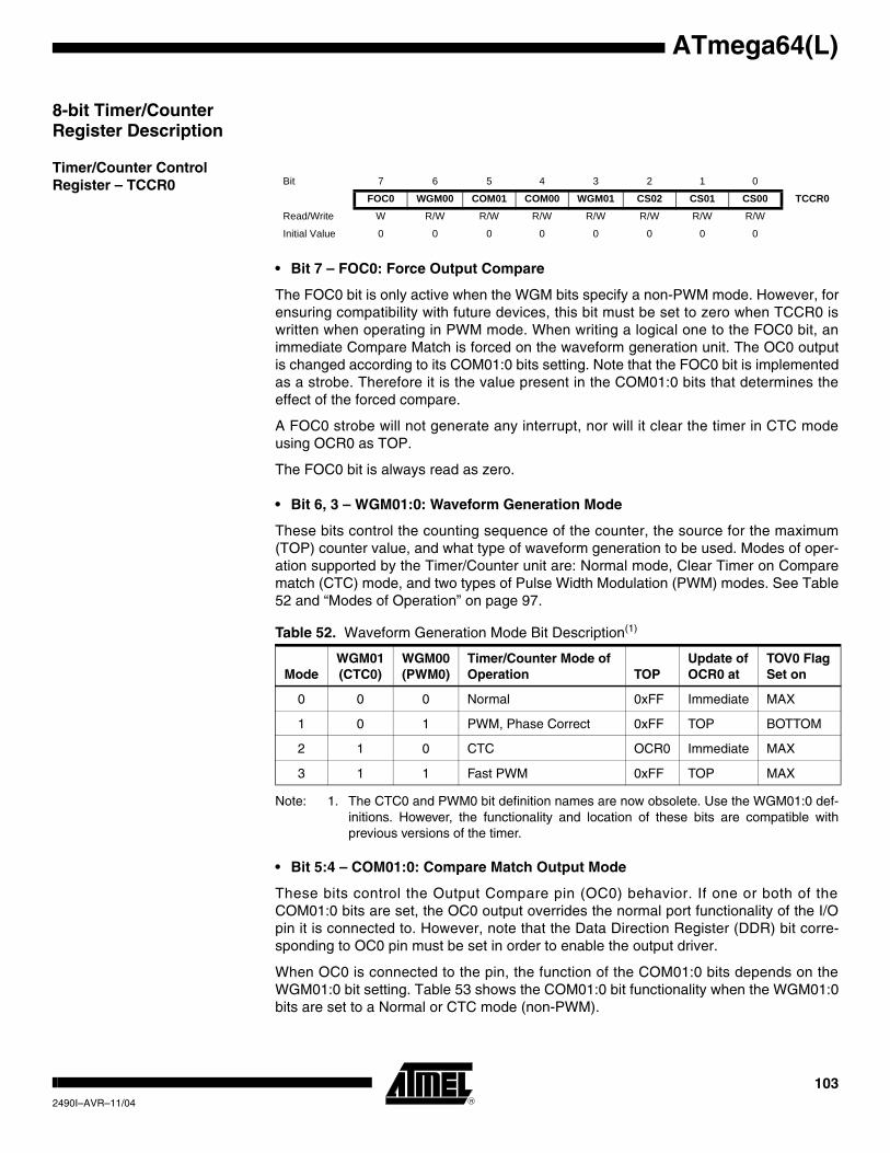
ATmega64(L)
8-bit Timer/Counter Register Description
Timer/Counter Control Register – TCCR0
• Bit 7 – FOC0: Force Output Compare
The FOC0 bit is only active when the WGM bits specify a non-PWM mode. However, forensuring compatibility with future devices, this bit must be set to zero when TCCR0 iswritten when operating in PWM mode. When writing a logical one to the FOC0 bit, animmediate Compare Match is forced on the waveform generation unit. The OC0 outputis changed according to its COM01:0 bits setting. Note that the FOC0 bit is implementedas a strobe. Therefore it is the value present in the COM01:0 bits that determines theeffect of the forced compare.
A FOC0 strobe will not generate any interrupt, nor will it clear the timer in CTC modeusing OCR0 as TOP.
The FOC0 bit is always read as zero.
• Bit 6, 3 – WGM01:0: Waveform Generation Mode
These bits control the counting sequence of the counter, the source for the maximum(TOP) counter value, and what type of waveform generation to be used. Modes of oper-ation supported by the Timer/Counter unit are: Normal mode, Clear Timer on Comparematch (CTC) mode, and two types of Pulse Width Modulation (PWM) modes. See Table52 and “Modes of Operation” on page 97.
Note: 1. The CTC0 and PWM0 bit definition names are now obsolete. Use the WGM01:0 def-initions. However, the functionality and location of these bits are compatible withprevious versions of the timer.
• Bit 5:4 – COM01:0: Compare Match Output Mode
These bits control the Output Compare pin (OC0) behavior. If one or both of theCOM01:0 bits are set, the OC0 output overrides the normal port functionality of the I/Opin it is connected to. However, note that the Data Direction Register (DDR) bit corre-sponding to OC0 pin must be set in order to enable the output driver.
When OC0 is connected to the pin, the function of the COM01:0 bits depends on theWGM01:0 bit setting. Table 53 shows the COM01:0 bit functionality when the WGM01:0bits are set to a Normal or CTC mode (non-PWM).
Bit 7 6 5 4 3 2 1 0
FOC0 WGM00 COM01 COM00 WGM01 CS02 CS01 CS00 TCCR0Read/Write W R/W R/W R/W R/W R/W R/W R/W
Initial Value 0 0 0 0 0 0 0 0
Table 52. Waveform Generation Mode Bit Description(1)
ModeWGM01(CTC0)
WGM00(PWM0)
Timer/Counter Mode of Operation TOP
Update ofOCR0 at
TOV0 FlagSet on
0 0 0 Normal 0xFF Immediate MAX
1 0 1 PWM, Phase Correct 0xFF TOP BOTTOM
2 1 0 CTC OCR0 Immediate MAX
3 1 1 Fast PWM 0xFF TOP MAX
1032490I–AVR–11/04
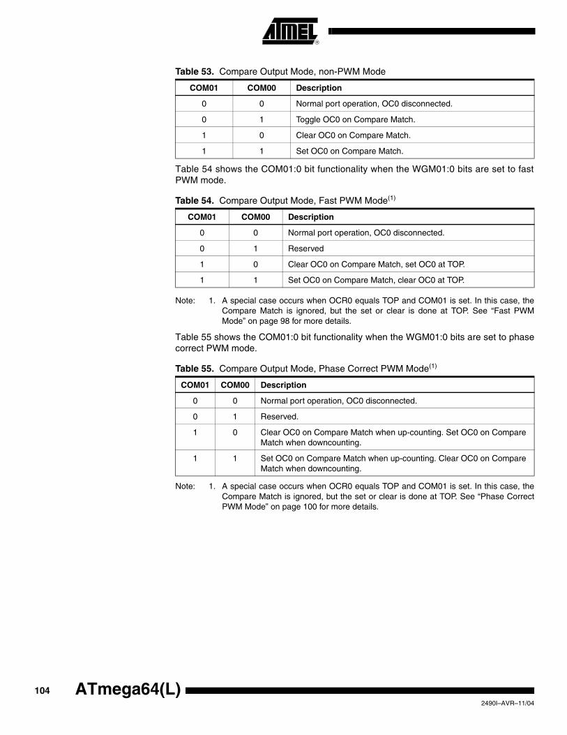
Table 54 shows the COM01:0 bit functionality when the WGM01:0 bits are set to fastPWM mode.
Note: 1. A special case occurs when OCR0 equals TOP and COM01 is set. In this case, theCompare Match is ignored, but the set or clear is done at TOP. See “Fast PWMMode” on page 98 for more details.
Table 55 shows the COM01:0 bit functionality when the WGM01:0 bits are set to phasecorrect PWM mode.
Note: 1. A special case occurs when OCR0 equals TOP and COM01 is set. In this case, theCompare Match is ignored, but the set or clear is done at TOP. See “Phase CorrectPWM Mode” on page 100 for more details.
Table 53. Compare Output Mode, non-PWM Mode
COM01 COM00 Description
0 0 Normal port operation, OC0 disconnected.
0 1 Toggle OC0 on Compare Match.
1 0 Clear OC0 on Compare Match.
1 1 Set OC0 on Compare Match.
Table 54. Compare Output Mode, Fast PWM Mode(1)
COM01 COM00 Description
0 0 Normal port operation, OC0 disconnected.
0 1 Reserved
1 0 Clear OC0 on Compare Match, set OC0 at TOP.
1 1 Set OC0 on Compare Match, clear OC0 at TOP.
Table 55. Compare Output Mode, Phase Correct PWM Mode(1)
COM01 COM00 Description
0 0 Normal port operation, OC0 disconnected.
0 1 Reserved.
1 0 Clear OC0 on Compare Match when up-counting. Set OC0 on Compare Match when downcounting.
1 1 Set OC0 on Compare Match when up-counting. Clear OC0 on Compare Match when downcounting.
104 ATmega64(L)2490I–AVR–11/04
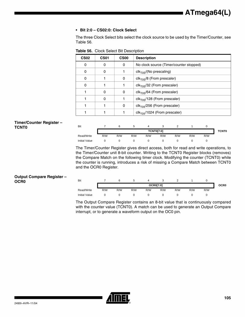
ATmega64(L)
• Bit 2:0 – CS02:0: Clock Select
The three Clock Select bits select the clock source to be used by the Timer/Counter, seeTable 56.
Timer/Counter Register – TCNT0
The Timer/Counter Register gives direct access, both for read and write operations, tothe Timer/Counter unit 8-bit counter. Writing to the TCNT0 Register blocks (removes)the Compare Match on the following timer clock. Modifying the counter (TCNT0) whilethe counter is running, introduces a risk of missing a Compare Match between TCNT0and the OCR0 Register.
Output Compare Register – OCR0
The Output Compare Register contains an 8-bit value that is continuously comparedwith the counter value (TCNT0). A match can be used to generate an Output Compareinterrupt, or to generate a waveform output on the OC0 pin.
Table 56. Clock Select Bit Description
CS02 CS01 CS00 Description
0 0 0 No clock source (Timer/counter stopped)
0 0 1 clkT0S/(No prescaling)
0 1 0 clkT0S/8 (From prescaler)
0 1 1 clkT0S/32 (From prescaler)
1 0 0 clkT0S/64 (From prescaler)
1 0 1 clkT0S/128 (From prescaler)
1 1 0 clkT0S/256 (From prescaler)
1 1 1 clkT0S/1024 (From prescaler)
Bit 7 6 5 4 3 2 1 0
TCNT0[7:0] TCNT0Read/Write R/W R/W R/W R/W R/W R/W R/W R/W
Initial Value 0 0 0 0 0 0 0 0
Bit 7 6 5 4 3 2 1 0
OCR0[7:0] OCR0Read/Write R/W R/W R/W R/W R/W R/W R/W R/W
Initial Value 0 0 0 0 0 0 0 0
1052490I–AVR–11/04
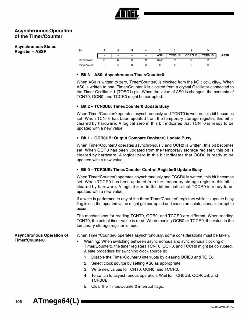
Asynchronous Operation of the Timer/Counter
Asynchronous Status Register – ASSR
• Bit 3 – AS0: Asynchronous Timer/Counter0
When AS0 is written to zero, Timer/Counter0 is clocked from the I/O clock, clkI/O. WhenAS0 is written to one, Timer/Counter 0 is clocked from a crystal Oscillator connected tothe Timer Oscillator 1 (TOSC1) pin. When the value of AS0 is changed, the contents ofTCNT0, OCR0, and TCCR0 might be corrupted.
• Bit 2 – TCN0UB: Timer/Counter0 Update Busy
When Timer/Counter0 operates asynchronously and TCNT0 is written, this bit becomesset. When TCNT0 has been updated from the temporary storage register, this bit iscleared by hardware. A logical zero in this bit indicates that TCNT0 is ready to beupdated with a new value.
• Bit 1 – OCR0UB: Output Compare Register0 Update Busy
When Timer/Counter0 operates asynchronously and OCR0 is written, this bit becomesset. When OCR0 has been updated from the temporary storage register, this bit iscleared by hardware. A logical zero in this bit indicates that OCR0 is ready to beupdated with a new value.
• Bit 0 – TCR0UB: Timer/Counter Control Register0 Update Busy
When Timer/Counter0 operates asynchronously and TCCR0 is written, this bit becomesset. When TCCR0 has been updated from the temporary storage register, this bit iscleared by hardware. A logical zero in this bit indicates that TCCR0 is ready to beupdated with a new value.
If a write is performed to any of the three Timer/Counter0 registers while its update busyflag is set, the updated value might get corrupted and cause an unintentional interrupt tooccur.
The mechanisms for reading TCNT0, OCR0, and TCCR0 are different. When readingTCNT0, the actual timer value is read. When reading OCR0 or TCCR0, the value in thetemporary storage register is read.
Asynchronous Operation of Timer/Counter0
When Timer/Counter0 operates asynchronously, some considerations must be taken.
• Warning: When switching between asynchronous and synchronous clocking of Timer/Counter0, the timer registers TCNT0, OCR0, and TCCR0 might be corrupted. A safe procedure for switching clock source is:
1. Disable the Timer/Counter0 interrupts by clearing OCIE0 and TOIE0.
2. Select clock source by setting AS0 as appropriate.
3. Write new values to TCNT0, OCR0, and TCCR0.
4. To switch to asynchronous operation: Wait for TCN0UB, OCR0UB, and TCR0UB.
5. Clear the Timer/Counter0 interrupt flags.
Bit 7 6 5 4 3 2 1 0
– – – – AS0 TCN0UB OCR0UB TCR0UB ASSRRead/Write R R R R R/W R R R
Initial Value 0 0 0 0 0 0 0 0
106 ATmega64(L)2490I–AVR–11/04
ATmega64(L)
6. Enable interrupts, if needed.
• The Oscillator is optimized for use with a 32.768 kHz watch crystal. Applying an external clock to the TOSC1 pin may result in incorrect Timer/Counter0 operation. The CPU main clock frequency must be more than four times the Oscillator frequency.
• When writing to one of the registers TCNT0, OCR0, or TCCR0, the value is transferred to a temporary register, and latched after two positive edges on TOSC1. The user should not write a new value before the contents of the temporary register have been transferred to its destination. Each of the three mentioned registers have their individual temporary register, for example, writing to TCNT0 does not disturb an OCR0 write in progress. To detect that a transfer to the destination register has taken place, the Asynchronous Status Register – ASSR has been implemented.
• When entering Power-save or Extended Standby mode after having written to TCNT0, OCR0, or TCCR0, the user must wait until the written register has been updated if Timer/Counter0 is used to wake up the device. Otherwise, the MCU will enter sleep mode before the changes are effective. This is particularly important if the Output Compare0 interrupt is used to wake up the device, since the Output Compare function is disabled during writing to OCR0 or TCNT0. If the write cycle is not finished, and the MCU enters sleep mode before the OCR0UB bit returns to zero, the device will never receive a Compare Match interrupt, and the MCU will not wake up.
• If Timer/Counter0 is used to wake the device up from Power-save or Extended Standby mode, precautions must be taken if the user wants to reenter one of these modes: The interrupt logic needs one TOSC1 cycle to be reset. If the time between wake-up and re-entering sleep mode is less than one TOSC1 cycle, the interrupt will not occur, and the device will fail to wake up. If the user is in doubt whether the time before re-entering Power-save or Extended Standby mode is sufficient, the following algorithm can be used to ensure that one TOSC1 cycle has elapsed:
1. Write a value to TCCR0, TCNT0, or OCR0.
2. Wait until the corresponding Update Busy flag in ASSR returns to zero.
3. Enter Power-save or Extended Standby mode.
• When the asynchronous operation is selected, the 32.768 kHz Oscillator for Timer/Counter0 is always running, except in Power-down and Standby modes. After a Power-up Reset or wake-up from Power-down or Standby mode, the user should be aware of the fact that this Oscillator might take as long as one second to stabilize. The user is advised to wait for at least one second before using Timer/Counter0 after Power-up or wake-up from Power-down or Standby mode. The contents of all Timer/Counter0 registers must be considered lost after a wake-up from Power-down or Standby mode due to unstable clock signal upon start-up, no matter whether the Oscillator is in use or a clock signal is applied to the TOSC1 pin.
• Description of wake up from Power-save or Extended Standby mode when the timer is clocked asynchronously: When the interrupt condition is met, the wake up process is started on the following cycle of the timer clock, that is, the timer is always advanced by at least one before the processor can read the counter value. After wake-up, the MCU is halted for four cycles, it executes the interrupt routine, and resumes execution from the instruction following SLEEP.
• Reading of the TCNT0 Register shortly after wake-up from Power-save may give an incorrect result. Since TCNT0 is clocked on the asynchronous TOSC clock, reading TCNT0 must be done through a register synchronized to the internal I/O clock domain. Synchronization takes place for every rising TOSC1 edge. When waking up from Power-save mode, and the I/O clock (clkI/O) again becomes active, TCNT0 will
1072490I–AVR–11/04
read as the previous value (before entering sleep) until the next rising TOSC1 edge. The phase of the TOSC clock after waking up from Power-save mode is essentially unpredictable, as it depends on the wake-up time. The recommended procedure for reading TCNT0 is thus as follows:
1. Write any value to either of the registers OCR0 or TCCR0.
2. Wait for the corresponding Update Busy Flag to be cleared.
3. Read TCNT0.
• During asynchronous operation, the synchronization of the interrupt flags for the asynchronous timer takes three processor cycles plus one timer cycle. The timer is therefore advanced by at least one before the processor can read the timer value causing the setting of the interrupt flag. The Output Compare pin is changed on the timer clock and is not synchronized to the processor clock.
Timer/Counter Interrupt Mask Register – TIMSK
• Bit 1 – OCIE0: Timer/Counter0 Output Compare Match Interrupt Enable
When the OCIE0 bit is written to one, and the I-bit in the Status Register is set (one), theTimer/Counter0 Compare Match interrupt is enabled. The corresponding interrupt isexecuted if a Compare Match in Timer/Counter0 occurs, i.e., when the OCF0 bit is set inthe Timer/Counter Interrupt Flag Register – TIFR.
• Bit 0 – TOIE0: Timer/Counter0 Overflow Interrupt Enable
When the TOIE0 bit is written to one, and the I-bit in the Status Register is set (one), theTimer/Counter0 Overflow interrupt is enabled. The corresponding interrupt is executed ifan overflow in Timer/Counter0 occurs, i.e., when the TOV0 bit is set in theTimer/Counter Interrupt Flag Register – TIFR.
Timer/Counter Interrupt Flag Register – TIFR
• Bit 1 – OCF0: Output Compare Flag 0
The OCF0 bit is set (one) when a Compare Match occurs between the Timer/Counter0and the data in OCR0 – Output Compare Register0. OCF0 is cleared by hardware whenexecuting the corresponding interrupt handling vector. Alternatively, OCF0 is cleared bywriting a logic one to the flag. When the I-bit in SREG, OCIE0 (Timer/Counter0 Com-pare Match Interrupt Enable), and OCF0 are set (one), the Timer/Counter0 CompareMatch Interrupt is executed.
Bit 7 6 5 4 3 2 1 0
OCIE2 TOIE2 TICIE1 OCIE1A OCIE1B TOIE1 OCIE0 TOIE0 TIMSK
Read/Write R/W R/W R/W R/W R/W R/W R/W R/W
Initial Value 0 0 0 0 0 0 0 0
Bit 7 6 5 4 3 2 1 0
OCF2 TOV2 ICF1 OCF1A OCF1B TOV1 OCF0 TOV0 TIFRRead/Write R/W R/W R/W R/W R/W R/W R/W R/W
Initial Value 0 0 0 0 0 0 0 0
108 ATmega64(L)2490I–AVR–11/04
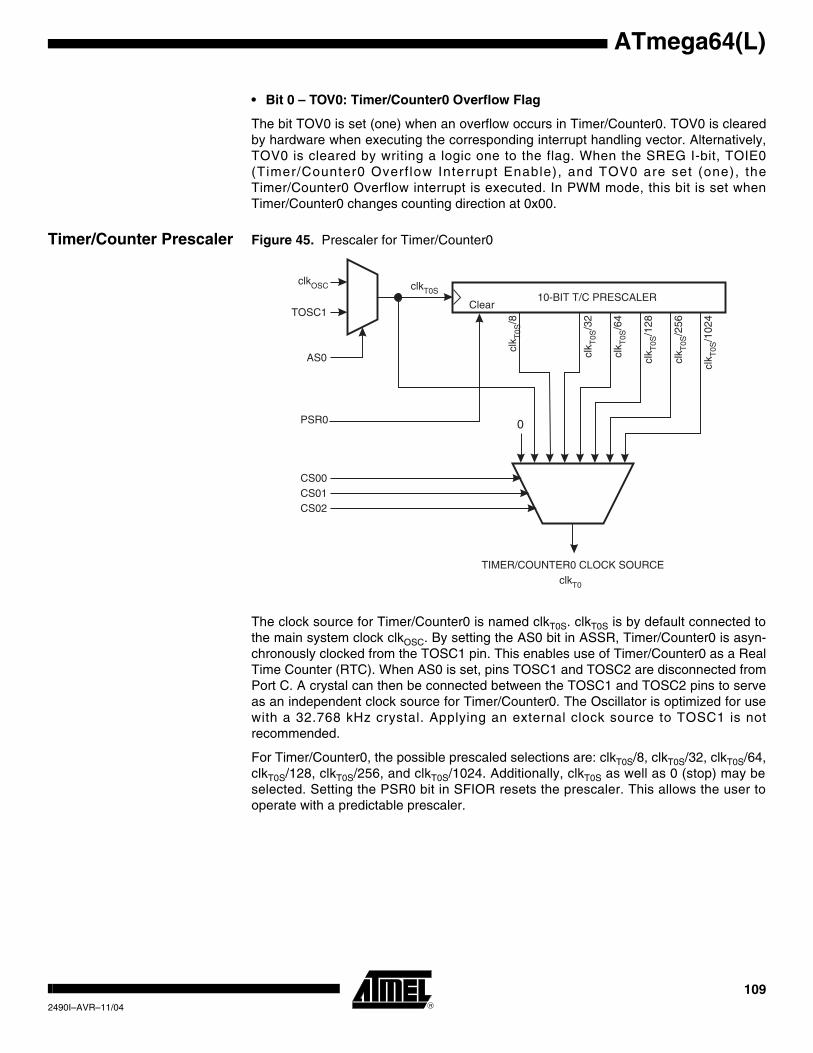
ATmega64(L)
• Bit 0 – TOV0: Timer/Counter0 Overflow Flag
The bit TOV0 is set (one) when an overflow occurs in Timer/Counter0. TOV0 is clearedby hardware when executing the corresponding interrupt handling vector. Alternatively,TOV0 is cleared by writing a logic one to the flag. When the SREG I-bit, TOIE0(Timer/Counter0 Overf low Interrupt Enable), and TOV0 are set (one), theTimer/Counter0 Overflow interrupt is executed. In PWM mode, this bit is set whenTimer/Counter0 changes counting direction at 0x00.
Timer/Counter Prescaler Figure 45. Prescaler for Timer/Counter0
The clock source for Timer/Counter0 is named clkT0S. clkT0S is by default connected tothe main system clock clkOSC. By setting the AS0 bit in ASSR, Timer/Counter0 is asyn-chronously clocked from the TOSC1 pin. This enables use of Timer/Counter0 as a RealTime Counter (RTC). When AS0 is set, pins TOSC1 and TOSC2 are disconnected fromPort C. A crystal can then be connected between the TOSC1 and TOSC2 pins to serveas an independent clock source for Timer/Counter0. The Oscillator is optimized for usewith a 32.768 kHz crystal. Applying an external clock source to TOSC1 is notrecommended.
For Timer/Counter0, the possible prescaled selections are: clkT0S/8, clkT0S/32, clkT0S/64,clkT0S/128, clkT0S/256, and clkT0S/1024. Additionally, clkT0S as well as 0 (stop) may beselected. Setting the PSR0 bit in SFIOR resets the prescaler. This allows the user tooperate with a predictable prescaler.
10-BIT T/C PRESCALER
TIMER/COUNTER0 CLOCK SOURCE
clkOSC clkT0S
TOSC1
AS0
CS00CS01CS02
clk T
0S/8
clk T
0S/6
4
clk T
0S/1
28
clk T
0S/1
024
clk T
0S/2
56
clk T
0S/3
2
0PSR0
Clear
clkT0
1092490I–AVR–11/04
Special Function IO Register – SFIOR
• Bit 7 – TSM: Timer/Counter Synchronization Mode
Writing TSM bit to one activates the Timer/Counter Synchronization mode. In this mode,the value that is written to PSR0 and PSR321 bits is kept, hence keeping the corre-sponding prescaler reset signals asserted. This ensures that the correspondingTimer/Counters are halted and can be configured to the same value without the risk ofone of them advancing during configuration. When the TSM bit written zero, the PSR0and PSR321 bits are cleared by hardware, and the Timer/Counters start countingsimultaneously.
• Bit 1 – PSR0: Prescaler Reset Timer/Counter0
When this bit is one, the Timer/Counter0 prescaler will be reset. The bit is normallycleared immediately by hardware. If this bit is written when Timer/Counter0 is operatingin Asynchronous mode, the bit will remain one until the prescaler has been reset. The bitwill not be cleared by hardware if the TSM bit is set.
Bit 7 6 5 4 3 2 1 0
TSM – – – ACME PUD PSR0 PSR321 SFIORRead/Write R/W R R R R/W R/W R/W R/W
Initial Value 0 0 0 0 0 0 0 0
110 ATmega64(L)2490I–AVR–11/04
ATmega64(L)
16-bit Timer/Counter (Timer/Counter1 and Timer/Counter3)
The 16-bit Timer/Counter unit allows accurate program execution timing (event man-agement), wave generation, and signal timing measurement. The main features are:• True 16-bit Design (i.e., Allows 16-bit PWM)• Three Independent Output Compare Units• Double Buffered Output Compare Registers• One Input Capture Unit• Input Capture Noise Canceler• Clear Timer on Compare Match (Auto Reload)• Glitch-free, Phase Correct Pulse Width Modulator (PWM)• Variable PWM Period• Frequency Generator• External Event Counter• Ten Independent Interrupt Sources (TOV1, OCF1A, OCF1B, OCF1C, ICF1, TOV3, OCF3A,
OCF3B, OCF3C, and ICF3)
Restrictions in ATmega103 Compatibility Mode
Note that in ATmega103 compatibility mode, only one 16-bit Timer/Counter is available(Timer/Counter1). Also note that in ATmega103 compatibility mode, the Timer/Counter1has two compare registers (Compare A and Compare B) only.
Overview Most register and bit references in this datasheet are written in general form. A lowercase “n” replaces the Timer/Counter number, and a lower case “x” replaces the OutputCompare unit channel. However, when using the register or bit defines in a program, theprecise form must be used (i.e,. TCNT1 for accessing Timer/Counter1 counter valueand so on). The physical I/O Register and bit locations for ATmega64 are listed in the“16-bit Timer/Counter Register Description” on page 132.
A simplified block diagram of the 16-bit Timer/Counter is shown in Figure 46. CPUaccessible I/O Registers, including I/O bits and I/O pins, are shown in bold.
1112490I–AVR–11/04

Figure 46. 16-bit Timer/Counter Block Diagram(1)
Note: 1. Refer to Figure 1 on page 2, Table 30 on page 73, and Table 39 on page 80 forTimer/Counter1 and 3 pin placement and description.
Registers The Timer/Counter (TCNTn), Output Compare Registers (OCRnA/B/C), and Input Cap-ture Register (ICRn) are all 16-bit registers. Special procedures must be followed whenaccessing the 16-bit registers. These procedures are described in the section “Access-ing 16-bit Registers” on page 114. The Timer/Counter Control Registers (TCCRnA/B/C)are 8-bit registers and have no CPU access restrictions. Interrupt requests (shorten asInt.Req.) signals are all visible in the Timer Interrupt Flag Register (TIFR) and ExtendedTimer Interrupt Flag Register (ETIFR). All interrupts are individually masked with theTimer Interrupt Mask Register (TIMSK) and Extended Timer Interrupt Mask Register(ETIMSK). (E)TIFR and (E)TIMSK are not shown in the figure since these registers areshared by other timer units.
The Timer/Counter can be clocked internally, via the prescaler, or by an external clocksource on the Tn pin. The Clock Select logic block controls which clock source and edgethe Timer/Counter uses to increment (or decrement) its value. The Timer/Counter isinactive when no clock source is selected. The output from the Clock Select logic isreferred to as the timer clock (clkTn).
ICFx (Int.Req.)
TOVx(Int.Req.)
Clock Select
Timer/Counter
DA
TA B
US
OCRxA
OCRxB
OCRxC
ICRx
=
=
=
TCNTx
WaveformGeneration
WaveformGeneration
WaveformGeneration
OCxA
OCxB
OCxC
NoiseCanceler
ICPx
=
FixedTOP
Values
EdgeDetector
Control Logic
= 0
TOP BOTTOM
Count
Clear
Direction
OCFxA(Int.Req.)
OCFxB(Int.Req.)
OCFxC(Int.Req.)
TCCRxA TCCRxB TCCRxC
( From AnalogComparator Ouput )
TxEdgeDetector
( From Prescaler )
TCLK
112 ATmega64(L)2490I–AVR–11/04
ATmega64(L)
The double buffered Output Compare Registers (OCRnA/B/C) are compared with theTimer/Counter value at all time. The result of the compare can be used by the WaveformGenerator to generate a PWM or variable frequency output on the Output Compare Pin(OCnA/B/C). See “Output Compare Units” on page 120. The Compare Match event willalso set the Compare Match Flag (OCFnA/B/C) which can be used to generate an Out-put Compare interrupt request.
The Input Capture Register can capture the Timer/Counter value at a given external(edge triggered) event on either the Input Capture pin (ICPn) or on the Analog Compar-ator pins (See “Analog Comparator” on page 228.) The Input Capture unit includes adigital filtering unit (Noise Canceler) for reducing the chance of capturing noise spikes.
The TOP value, or maximum Timer/Counter value, can in some modes of operation bedefined by either the OCRnA Register, the ICRn Register, or by a set of fixed values.When using OCRnA as TOP value in a PWM mode, the OCRnA Register can not beused for generating a PWM output. However, the TOP value will in this case be doublebuffered allowing the TOP value to be changed in run time. If a fixed TOP value isrequired, the ICRn Register can be used as an alternative, freeing the OCRnA to beused as PWM output.
Definitions The following definitions are used extensively throughout this section:
Compatibility The 16-bit Timer/Counter has been updated and improved from previous versions of the16-bit AVR Timer/Counter. This 16-bit Timer/Counter is fully compatible with the earlierversion regarding:
• All 16-bit Timer/Counter related I/O Register address locations, including Timer Interrupt Registers.
• Bit locations inside all 16-bit Timer/Counter registers, including Timer Interrupt Registers.
• Interrupt Vectors.
The following control bits have changed name, but have same functionality and registerlocation:
• PWMn0 is changed to WGMn0.
• PWMn1 is changed to WGMn1.
• CTCn is changed to WGMn2.
The following registers are added to the 16-bit Timer/Counter:
• Timer/Counter Control Register C (TCCRnC).
• Output Compare Register C, OCRnCH and OCRnCL, combined OCRnC.
The following bits are added to the 16-bit Timer/Counter control registers:
• COM1C1:0 are added to TCCR1A.
Table 57. Definitions
BOTTOM The counter reaches the BOTTOM when it becomes 0x0000.
MAX The counter reaches its MAXimum when it becomes 0xFFFF (decimal65535).
TOP The counter reaches the TOP when it becomes equal to the highestvalue in the count sequence. The TOP value can be assigned to be oneof the fixed values: 0x00FF, 0x01FF, or 0x03FF, or to the value stored inthe OCRnA or ICRn Register. The assignment is dependent of the modeof operation.
1132490I–AVR–11/04
• FOCnA, FOCnB, and FOCnC are added in the new TCCRnC Register.
• WGMn3 is added to TCCRnB.
Interrupt flag and mask bits for Output Compare unit C are added.
The 16-bit Timer/Counter has improvements that will affect the compatibility in somespecial cases.
Accessing 16-bit Registers
The TCNTn, OCRnA/B/C, and ICRn are 16-bit registers that can be accessed by theAVR CPU via the 8-bit data bus. The 16-bit register must be byte accessed using tworead or write operations. Each 16-bit timer has a single 8-bit register for temporary stor-ing of the high byte of the 16-bit access. The same temporary register is sharedbetween all 16-bit registers within each 16-bit timer. Accessing the low byte triggers the16-bit read or write operation. When the low byte of a 16-bit register is written by theCPU, the high byte stored in the temporary register, and the low byte written are bothcopied into the 16-bit register in the same clock cycle. When the low byte of a 16-bit reg-ister is read by the CPU, the high byte of the 16-bit register is copied into the temporaryregister in the same clock cycle as the low byte is read.
Not all 16-bit accesses uses the temporary register for the high byte. Reading theOCRnA/B/C 16-bit registers does not involve using the temporary register.
To do a 16-bit write, the high byte must be written before the low byte. For a 16-bit read,the low byte must be read before the high byte.
The following code examples show how to access the 16-bit timer registers assumingthat no interrupts updates the temporary register. The same principle can be useddirectly for accessing the OCRnA/B/C and ICRn Registers. Note that when using “C”,the compiler handles the 16-bit access.
Note: 1. The example code assumes that the part specific header file is included.For I/O Registers located in extended I/O map, “IN”, “OUT”, “SBIS”, “SBIC”, “CBI”,and “SBI” instructions must be replaced with instructions that allow access to
Assembly Code Examples(1)
...
; Set TCNTn to 0x01FFldi r17,0x01
ldi r16,0xFF
out TCNTnH,r17out TCNTnL,r16; Read TCNTn into r17:r16in r16,TCNTnLin r17,TCNTnH...
C Code Examples(1)
unsigned int i;
...
/* Set TCNTn to 0x01FF */TCNTn = 0x1FF;/* Read TCNTn into i */i = TCNTn;...
114 ATmega64(L)2490I–AVR–11/04
ATmega64(L)
extended I/O. Typically “LDS” and “STS” combined with “SBRS”, “SBRC”, “SBR”, and“CBR”.
The assembly code example returns the TCNTn value in the r17:r16 register pair.
It is important to notice that accessing 16-bit registers are atomic operations. If an inter-rupt occurs between the two instructions accessing the 16-bit register, and the interruptcode updates the temporary register by accessing the same or any other of the 16-bittimer registers, then the result of the access outside the interrupt will be corrupted.Therefore, when both the main code and the interrupt code update the temporary regis-ter, the main code must disable the interrupts during the 16-bit access.
The following code examples show how to do an atomic read of the TCNTn Registercontents. Reading any of the OCRnA/B/C or ICRn Registers can be done by using thesame principle.
Note: 1. The example code assumes that the part specific header file is included.For I/O Registers located in extended I/O map, “IN”, “OUT”, “SBIS”, “SBIC”, “CBI”,and “SBI” instructions must be replaced with instructions that allow access toextended I/O. Typically “LDS” and “STS” combined with “SBRS”, “SBRC”, “SBR”, and“CBR”.
The assembly code example returns the TCNTn value in the r17:r16 register pair.
Assembly Code Example(1)
TIM16_ReadTCNTn:; Save global interrupt flag
in r18,SREG
; Disable interrupts
cli
; Read TCNTn into r17:r16in r16,TCNTnLin r17,TCNTnH; Restore global interrupt flag
out SREG,r18
ret
C Code Example(1)
unsigned int TIM16_ReadTCNTn( void )
unsigned char sreg;
unsigned int i;
/* Save global interrupt flag */
sreg = SREG;
/* Disable interrupts */
_CLI();
/* Read TCNTn into i */i = TCNTn;/* Restore global interrupt flag */
SREG = sreg;
return i;
1152490I–AVR–11/04
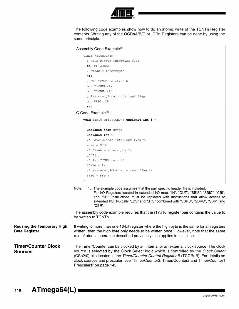
The following code examples show how to do an atomic write of the TCNTn Registercontents. Writing any of the OCRnA/B/C or ICRn Registers can be done by using thesame principle.
Note: 1. The example code assumes that the part specific header file is included.For I/O Registers located in extended I/O map, “IN”, “OUT”, “SBIS”, “SBIC”, “CBI”,and “SBI” instructions must be replaced with instructions that allow access toextended I/O. Typically “LDS” and “STS” combined with “SBRS”, “SBRC”, “SBR”, and“CBR”.
The assembly code example requires that the r17:r16 register pair contains the value tobe written to TCNTn.
Reusing the Temporary High Byte Register
If writing to more than one 16-bit register where the high byte is the same for all registerswritten, then the high byte only needs to be written once. However, note that the samerule of atomic operation described previously also applies in this case.
Timer/Counter Clock Sources
The Timer/Counter can be clocked by an internal or an external clock source. The clocksource is selected by the Clock Select logic which is controlled by the Clock Select(CSn2:0) bits located in the Timer/Counter Control Register B (TCCRnB). For details onclock sources and prescaler, see “Timer/Counter3, Timer/Counter2 and Timer/Counter1Prescalers” on page 143.
Assembly Code Example(1)
TIM16_WriteTCNTn:; Save global interrupt flag
in r18,SREG
; Disable interrupts
cli
; Set TCNTn to r17:r16out TCNTnH,r17out TCNTnL,r16; Restore global interrupt flag
out SREG,r18
ret
C Code Example(1)
void TIM16_WriteTCNTn( unsigned int i )
unsigned char sreg;
unsigned int i;
/* Save global interrupt flag */
sreg = SREG;
/* Disable interrupts */
_CLI();
/* Set TCNTn to i */TCNTn = i;/* Restore global interrupt flag */
SREG = sreg;
116 ATmega64(L)2490I–AVR–11/04
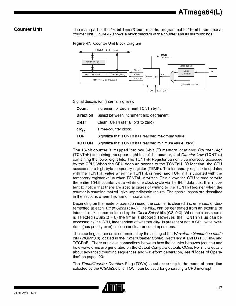
ATmega64(L)
Counter Unit The main part of the 16-bit Timer/Counter is the programmable 16-bit bi-directionalcounter unit. Figure 47 shows a block diagram of the counter and its surroundings.
Figure 47. Counter Unit Block Diagram
Signal description (internal signals):
Count Increment or decrement TCNTn by 1.
Direction Select between increment and decrement.
Clear Clear TCNTn (set all bits to zero).
clkTn Timer/counter clock.
TOP Signalize that TCNTn has reached maximum value.
BOTTOM Signalize that TCNTn has reached minimum value (zero).
The 16-bit counter is mapped into two 8-bit I/O memory locations: Counter High(TCNTnH) containing the upper eight bits of the counter, and Counter Low (TCNTnL)containing the lower eight bits. The TCNTnH Register can only be indirectly accessedby the CPU. When the CPU does an access to the TCNTnH I/O location, the CPUaccesses the high byte temporary register (TEMP). The temporary register is updatedwith the TCNTnH value when the TCNTnL is read, and TCNTnH is updated with thetemporary register value when TCNTnL is written. This allows the CPU to read or writethe entire 16-bit counter value within one clock cycle via the 8-bit data bus. It is impor-tant to notice that there are special cases of writing to the TCNTn Register when thecounter is counting that will give unpredictable results. The special cases are describedin the sections where they are of importance.
Depending on the mode of operation used, the counter is cleared, incremented, or dec-remented at each Timer Clock (clkTn). The clkTn can be generated from an external orinternal clock source, selected by the Clock Select bits (CSn2:0). When no clock sourceis selected (CSn2:0 = 0) the timer is stopped. However, the TCNTn value can beaccessed by the CPU, independent of whether clkTn is present or not. A CPU write over-rides (has priority over) all counter clear or count operations.
The counting sequence is determined by the setting of the Waveform Generation modebits (WGMn3:0) located in the Timer/Counter Control Registers A and B (TCCRnA andTCCRnB). There are close connections between how the counter behaves (counts) andhow waveforms are generated on the Output Compare outputs OCnx. For more detailsabout advanced counting sequences and waveform generation, see “Modes of Opera-tion” on page 123.
The Timer/Counter Overflow Flag (TOVn) is set according to the mode of operationselected by the WGMn3:0 bits. TOVn can be used for generating a CPU interrupt.
TEMP (8-bit)
DATA BUS (8-bit)
TCNTn (16-bit Counter)
TCNTnH (8-bit) TCNTnL (8-bit)Control Logic
Count
Clear
Direction
TOVn(Int.Req.)
Clock Select
TOP BOTTOM
TnEdge
Detector
( From Prescaler )
clkTn
1172490I–AVR–11/04
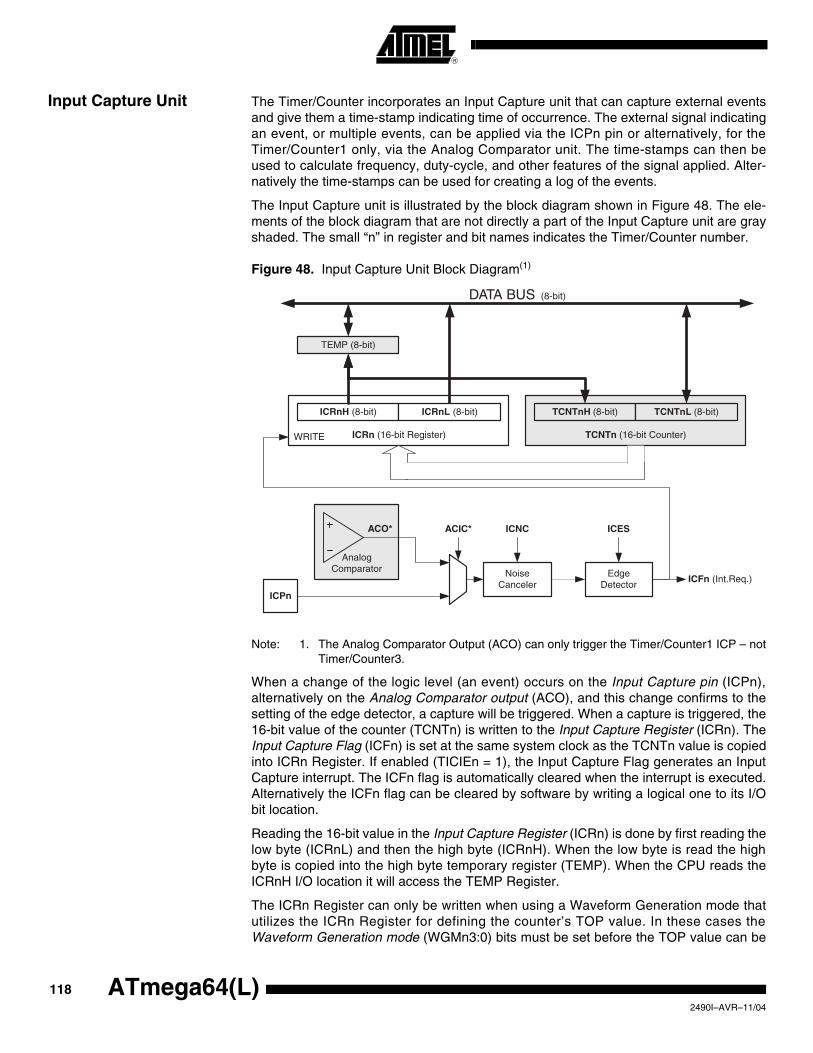
Input Capture Unit The Timer/Counter incorporates an Input Capture unit that can capture external eventsand give them a time-stamp indicating time of occurrence. The external signal indicatingan event, or multiple events, can be applied via the ICPn pin or alternatively, for theTimer/Counter1 only, via the Analog Comparator unit. The time-stamps can then beused to calculate frequency, duty-cycle, and other features of the signal applied. Alter-natively the time-stamps can be used for creating a log of the events.
The Input Capture unit is illustrated by the block diagram shown in Figure 48. The ele-ments of the block diagram that are not directly a part of the Input Capture unit are grayshaded. The small “n” in register and bit names indicates the Timer/Counter number.
Figure 48. Input Capture Unit Block Diagram(1)
Note: 1. The Analog Comparator Output (ACO) can only trigger the Timer/Counter1 ICP – notTimer/Counter3.
When a change of the logic level (an event) occurs on the Input Capture pin (ICPn),alternatively on the Analog Comparator output (ACO), and this change confirms to thesetting of the edge detector, a capture will be triggered. When a capture is triggered, the16-bit value of the counter (TCNTn) is written to the Input Capture Register (ICRn). TheInput Capture Flag (ICFn) is set at the same system clock as the TCNTn value is copiedinto ICRn Register. If enabled (TICIEn = 1), the Input Capture Flag generates an InputCapture interrupt. The ICFn flag is automatically cleared when the interrupt is executed.Alternatively the ICFn flag can be cleared by software by writing a logical one to its I/Obit location.
Reading the 16-bit value in the Input Capture Register (ICRn) is done by first reading thelow byte (ICRnL) and then the high byte (ICRnH). When the low byte is read the highbyte is copied into the high byte temporary register (TEMP). When the CPU reads theICRnH I/O location it will access the TEMP Register.
The ICRn Register can only be written when using a Waveform Generation mode thatutilizes the ICRn Register for defining the counter’s TOP value. In these cases theWaveform Generation mode (WGMn3:0) bits must be set before the TOP value can be
ICFn (Int.Req.)
AnalogComparator
WRITE ICRn (16-bit Register)
ICRnH (8-bit)
NoiseCanceler
ICPn
EdgeDetector
TEMP (8-bit)
DATA BUS (8-bit)
ICRnL (8-bit)
TCNTn (16-bit Counter)
TCNTnH (8-bit) TCNTnL (8-bit)
ACIC* ICNC ICESACO*
118 ATmega64(L)2490I–AVR–11/04
ATmega64(L)
written to the ICRn Register. When writing the ICRn Register the high byte must be writ-ten to the ICRnH I/O location before the low byte is written to ICRnL.
For more information on how to access the 16-bit registers refer to “Accessing 16-bitRegisters” on page 114.
Input Capture Source The main trigger source for the Input Capture unit is the Input Capture pin (ICPn).Timer/Counter1 can alternatively use the Analog Comparator output as trigger sourcefor the Input Capture unit. The Analog Comparator is selected as trigger source by set-ting the Analog Comparator Input Capture (ACIC) bit in the Analog Comparator Controland Status Register (ACSR). Be aware that changing trigger source can trigger a cap-ture. The Input Capture Flag must therefore be cleared after the change.
Both the Input Capture pin (ICPn) and the Analog Comparator output (ACO) inputs aresampled using the same technique as for the Tn pin (Figure 59 on page 143). The edgedetector is also identical. However, when the noise canceler is enabled, additional logicis inserted before the edge detector, which increases the delay by four system clockcycles. Note that the input of the noise canceler and edge detector is always enabledunless the Timer/Counter is set in a Waveform Generation mode that uses ICRn todefine TOP.
An Input Capture can be triggered by software by controlling the port of the ICPn pin.
Noise Canceler The Noise Canceler improves noise immunity by using a simple digital filtering scheme.The Noise Canceler input is monitored over four samples, and all four must be equal forchanging the output that in turn is used by the edge detector.
The Noise Canceler is enabled by setting the Input Capture Noise Canceler (ICNCn) bitin Timer/Counter Control Register B (TCCRnB). When enabled the Noise Cancelerintroduces additional four system clock cycles of delay from a change applied to theinput, to the update of the ICRn Register. The Noise Canceler uses the system clockand is therefore not affected by the prescaler.
Using the Input Capture Unit The main challenge when using the Input Capture unit is to assign enough processorcapacity for handling the incoming events. The time between two events is critical. If theprocessor has not read the captured value in the ICRn Register before the next eventoccurs, the ICRn will be overwritten with a new value. In this case the result of the cap-ture will be incorrect.
When using the Input Capture interrupt, the ICRn Register should be read as early in theinterrupt handler routine as possible. Even though the Input Capture interrupt has rela-tively high priority, the maximum interrupt response time is dependent on the maximumnumber of clock cycles it takes to handle any of the other interrupt requests.
Using the Input Capture unit in any mode of operation when the TOP value (resolution)is actively changed during operation, is not recommended.
Measurement of an external signal’s duty cycle requires that the trigger edge is changedafter each capture. Changing the edge sensing must be done as early as possible afterthe ICRn Register has been read. After a change of the edge, the Input Capture Flag(ICFn) must be cleared by software (writing a logical one to the I/O bit location). Formeasuring frequency only, the clearing of the ICFn flag is not required (if an interrupthandler is used).
1192490I–AVR–11/04
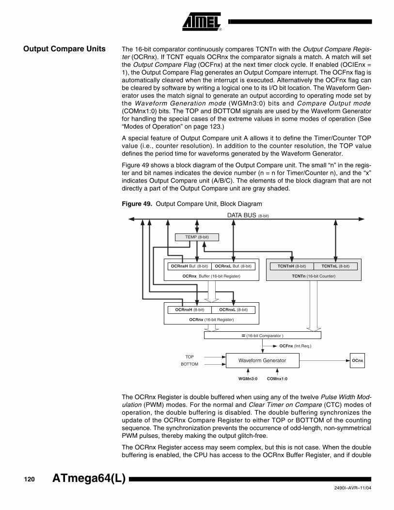
Output Compare Units The 16-bit comparator continuously compares TCNTn with the Output Compare Regis-ter (OCRnx). If TCNT equals OCRnx the comparator signals a match. A match will setthe Output Compare Flag (OCFnx) at the next timer clock cycle. If enabled (OCIEnx =1), the Output Compare Flag generates an Output Compare interrupt. The OCFnx flag isautomatically cleared when the interrupt is executed. Alternatively the OCFnx flag canbe cleared by software by writing a logical one to its I/O bit location. The Waveform Gen-erator uses the match signal to generate an output according to operating mode set bythe Waveform Generation mode (WGMn3:0) bits and Compare Output mode(COMnx1:0) bits. The TOP and BOTTOM signals are used by the Waveform Generatorfor handling the special cases of the extreme values in some modes of operation (See“Modes of Operation” on page 123.)
A special feature of Output Compare unit A allows it to define the Timer/Counter TOPvalue (i.e., counter resolution). In addition to the counter resolution, the TOP valuedefines the period time for waveforms generated by the Waveform Generator.
Figure 49 shows a block diagram of the Output Compare unit. The small “n” in the regis-ter and bit names indicates the device number (n = n for Timer/Counter n), and the “x”indicates Output Compare unit (A/B/C). The elements of the block diagram that are notdirectly a part of the Output Compare unit are gray shaded.
Figure 49. Output Compare Unit, Block Diagram
The OCRnx Register is double buffered when using any of the twelve Pulse Width Mod-ulation (PWM) modes. For the normal and Clear Timer on Compare (CTC) modes ofoperation, the double buffering is disabled. The double buffering synchronizes theupdate of the OCRnx Compare Register to either TOP or BOTTOM of the countingsequence. The synchronization prevents the occurrence of odd-length, non-symmetricalPWM pulses, thereby making the output glitch-free.
The OCRnx Register access may seem complex, but this is not case. When the doublebuffering is enabled, the CPU has access to the OCRnx Buffer Register, and if double
OCFnx (Int.Req.)
= (16-bit Comparator )
OCRnx Buffer (16-bit Register)
OCRnxH Buf. (8-bit)
OCnx
TEMP (8-bit)
DATA BUS (8-bit)
OCRnxL Buf. (8-bit)
TCNTn (16-bit Counter)
TCNTnH (8-bit) TCNTnL (8-bit)
COMnx1:0WGMn3:0
OCRnx (16-bit Register)
OCRnxH (8-bit) OCRnxL (8-bit)
Waveform GeneratorTOP
BOTTOM
120 ATmega64(L)2490I–AVR–11/04
ATmega64(L)
buffering is disabled the CPU will access the OCRnx directly. The content of the OCR1x(Buffer or Compare) Register is only changed by a write operation (the Timer/Counterdoes not update this register automatically as the TCNTn – and ICRn Register). There-fore OCRnx is not read via the high byte temporary register (TEMP). However, it is agood practice to read the low byte first as when accessing other 16-bit registers. Writingthe OCRnx registers must be done via the TEMP Register since the compare of all 16bits is done continuously. The high byte (OCRnxH) has to be written first. When the highbyte I/O location is written by the CPU, the TEMP Register will be updated by the valuewritten. Then when the low byte (OCRnxL) is written to the lower eight bits, the high bytewill be copied into the upper eight bits of either the OCRnx Buffer or OCRnx CompareRegister in the same system clock cycle.
For more information of how to access the 16-bit registers refer to “Accessing 16-bitRegisters” on page 114.
Force Output Compare In non-PWM waveform generation modes, the match output of the comparator can beforced by writing a one to the Force Output Compare (FOCnx) bit. Forcing CompareMatch will not set the OCFnx flag or reload/clear the timer, but the OCnx pin will beupdated as if a real Compare Match had occurred (the COMn1:0 bits settings definewhether the OCnx pin is set, cleared or toggled).
Compare Match Blocking by TCNTn Write
All CPU writes to the TCNTn Register will block any Compare Match that occurs in thenext timer clock cycle, even when the timer is stopped. This feature allows OCRnx to beinitialized to the same value as TCNTn without triggering an interrupt when theTimer/Counter clock is enabled.
Using the Output Compare Unit
Since writing TCNTn in any mode of operation will block all Compare Matches for onetimer clock cycle, there are risks involved when changing TCNTn when using any of theOutput Compare channels, independent of whether the Timer/Counter is running or not.If the value written to TCNTn equals the OCRnx value, the Compare Match will bemissed, resulting in incorrect waveform generation. Do not write the TCNTn equal toTOP in PWM modes with variable TOP values. The Compare Match for the TOP will beignored and the counter will continue to 0xFFFF. Similarly, do not write the TCNTn valueequal to BOTTOM when the counter is downcounting.
The setup of the OCnx should be performed before setting the Data Direction Registerfor the port pin to output. The easiest way of setting the OCnx value is to use the ForceOutput Compare (FOCnx) strobe bits in Normal mode. The OCnx Register keeps itsvalue even when changing between waveform generation modes.
Be aware that the COMnx1:0 bits are not double buffered together with the comparevalue. Changing the COMnx1:0 bits will take effect immediately.
Compare Match Output Unit
The Compare Output mode (COMnx1:0) bits have two functions. The Waveform Gener-ator uses the COMnx1:0 bits for defining the Output Compare (OCnx) state at the nextCompare Match. Secondly the COMnx1:0 bits control the OCnx pin output source. Fig-ure 50 shows a simplified schematic of the logic affected by the COMnx1:0 bit setting.The I/O Registers, I/O bits, and I/O pins in the figure are shown in bold. Only the parts ofthe general I/O port control registers (DDR and PORT) that are affected by theCOMnx1:0 bits are shown. When referring to the OCnx state, the reference is for theinternal OCnx Register, not the OCnx pin. If a System Reset occur, the OCnx Register isreset to “0”.
1212490I–AVR–11/04
Figure 50. Compare Match Output Unit, Schematic
The general I/O port function is overridden by the Output Compare (OCnx) from theWaveform Generator if either of the COMnx1:0 bits are set. However, the OCnx pindirection (input or output) is still controlled by the Data Direction Register (DDR) for theport pin. The Data Direction Register bit for the OCnx pin (DDR_OCnx) must be set asoutput before the OCnx value is visible on the pin. The port override function is generallyindependent of the Waveform Generation mode, but there are some exceptions. Referto Table 58, Table 59 and Table 60 for details.
The design of the Output Compare pin logic allows initialization of the OCnx state beforethe output is enabled. Note that some COMnx1:0 bit settings are reserved for certainmodes of operation. See “16-bit Timer/Counter Register Description” on page 132.
The COMnx1:0 bits have no effect on the Input Capture unit.
Compare Output Mode and Waveform Generation
The Waveform Generator uses the COMnx1:0 bits differently in Normal, CTC, and PWMmodes. For all modes, setting the COMnx1:0 = 0 tells the Waveform Generator that noaction on the OCnx Register is to be performed on the next Compare Match. For com-pare output actions in the non-PWM modes refer to Table 58 on page 133. For fastPWM mode refer to Table 59 on page 133, and for phase correct and phase and fre-quency correct PWM refer to Table 60 on page 134.
A change of the COMnx1:0 bits state will have effect at the first Compare Match afterthe bits are written. For non-PWM modes, the action can be forced to have immediateeffect by using the FOCnx strobe bits.
PORT
DDR
D Q
D Q
OCnxPinOCnx
D QWaveformGenerator
COMnx1
COMnx0
0
1
DAT
A B
US
FOCnx
clkI/O
122 ATmega64(L)2490I–AVR–11/04
ATmega64(L)
Modes of Operation The mode of operation, i.e., the behavior of the Timer/Counter and the Output Comparepins, is defined by the combination of the Waveform Generation mode (WGMn3:0) andCompare Output mode (COMnx1:0) bits. The Compare Output mode bits do not affectthe counting sequence, while the Waveform Generation mode bits do. The COMnx1:0bits control whether the PWM output generated should be inverted or not (inverted ornon-inverted PWM). For non-PWM modes the COMnx1:0 bits control whether the out-put should be set, cleared or toggle at a Compare Match (See “Compare Match OutputUnit” on page 121.)
For detailed timing information refer to “Timer/Counter Timing Diagrams” on page 130.
Normal Mode The simplest mode of operation is the Normal mode (WGMn3:0 = 0). In this mode thecounting direction is always up (incrementing), and no counter clear is performed. Thecounter simply overruns when it passes its maximum 16-bit value (MAX = 0xFFFF) andthen restarts from the BOTTOM (0x0000). In normal operation the Timer/Counter Over-flow Flag (TOVn) will be set in the same timer clock cycle as the TCNTn becomes zero.The TOVn flag in this case behaves like a 17th bit, except that it is only set, not cleared.However, combined with the timer overflow interrupt that automatically clears the TOVnflag, the timer resolution can be increased by software. There are no special cases toconsider in the Normal mode, a new counter value can be written anytime.
The Input Capture unit is easy to use in Normal mode. However, observe that the maxi-mum interval between the external events must not exceed the resolution of the counter.If the interval between events are too long, the timer overflow interrupt or the prescalermust be used to extend the resolution for the capture unit.
The Output Compare units can be used to generate interrupts at some given time. Usingthe Output Compare to generate waveforms in Normal mode is not recommended,since this will occupy too much of the CPU time.
Clear Timer on Compare Match (CTC) Mode
In Clear Timer on Compare or CTC mode (WGMn3:0 = 4 or 12), the OCRnA or ICRnRegister are used to manipulate the counter resolution. In CTC mode the counter iscleared to zero when the counter value (TCNTn) matches either the OCRnA (WGMn3:0= 4) or the ICRn (WGMn3:0 = 12). The OCRnA or ICRn define the top value for thecounter, hence also its resolution. This mode allows greater control of the CompareMatch output frequency. It also simplifies the operation of counting external events.
The timing diagram for the CTC mode is shown in Figure 51. The counter value(TCNTn) increases until a Compare Match occurs with either OCRnA or ICRn, and thencounter (TCNTn) is cleared.
1232490I–AVR–11/04
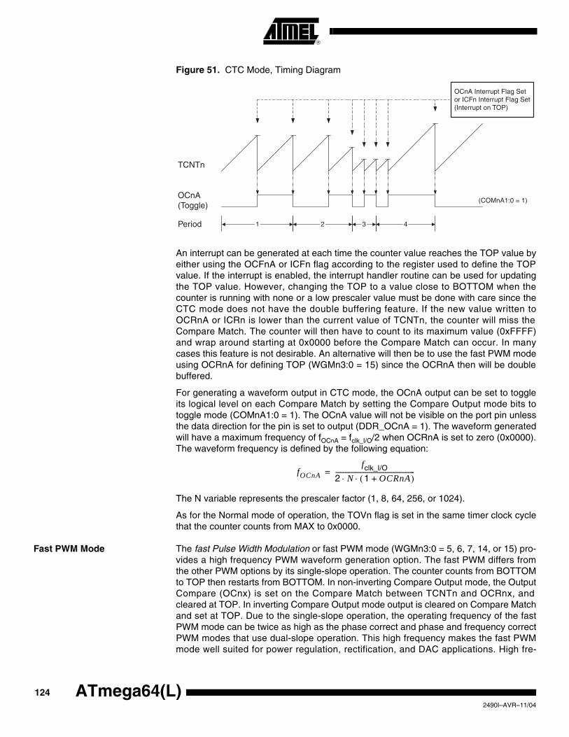
Figure 51. CTC Mode, Timing Diagram
An interrupt can be generated at each time the counter value reaches the TOP value byeither using the OCFnA or ICFn flag according to the register used to define the TOPvalue. If the interrupt is enabled, the interrupt handler routine can be used for updatingthe TOP value. However, changing the TOP to a value close to BOTTOM when thecounter is running with none or a low prescaler value must be done with care since theCTC mode does not have the double buffering feature. If the new value written toOCRnA or ICRn is lower than the current value of TCNTn, the counter will miss theCompare Match. The counter will then have to count to its maximum value (0xFFFF)and wrap around starting at 0x0000 before the Compare Match can occur. In manycases this feature is not desirable. An alternative will then be to use the fast PWM modeusing OCRnA for defining TOP (WGMn3:0 = 15) since the OCRnA then will be doublebuffered.
For generating a waveform output in CTC mode, the OCnA output can be set to toggleits logical level on each Compare Match by setting the Compare Output mode bits totoggle mode (COMnA1:0 = 1). The OCnA value will not be visible on the port pin unlessthe data direction for the pin is set to output (DDR_OCnA = 1). The waveform generatedwill have a maximum frequency of fOCnA = fclk_I/O/2 when OCRnA is set to zero (0x0000).The waveform frequency is defined by the following equation:
The N variable represents the prescaler factor (1, 8, 64, 256, or 1024).
As for the Normal mode of operation, the TOVn flag is set in the same timer clock cyclethat the counter counts from MAX to 0x0000.
Fast PWM Mode The fast Pulse Width Modulation or fast PWM mode (WGMn3:0 = 5, 6, 7, 14, or 15) pro-vides a high frequency PWM waveform generation option. The fast PWM differs fromthe other PWM options by its single-slope operation. The counter counts from BOTTOMto TOP then restarts from BOTTOM. In non-inverting Compare Output mode, the OutputCompare (OCnx) is set on the Compare Match between TCNTn and OCRnx, andcleared at TOP. In inverting Compare Output mode output is cleared on Compare Matchand set at TOP. Due to the single-slope operation, the operating frequency of the fastPWM mode can be twice as high as the phase correct and phase and frequency correctPWM modes that use dual-slope operation. This high frequency makes the fast PWMmode well suited for power regulation, rectification, and DAC applications. High fre-
TCNTn
OCnA(Toggle)
OCnA Interrupt Flag Setor ICFn Interrupt Flag Set(Interrupt on TOP)
1 4Period 2 3
(COMnA1:0 = 1)
fOCnAfclk_I/O
2 N 1 OCRnA+( )⋅ ⋅---------------------------------------------------=
124 ATmega64(L)2490I–AVR–11/04
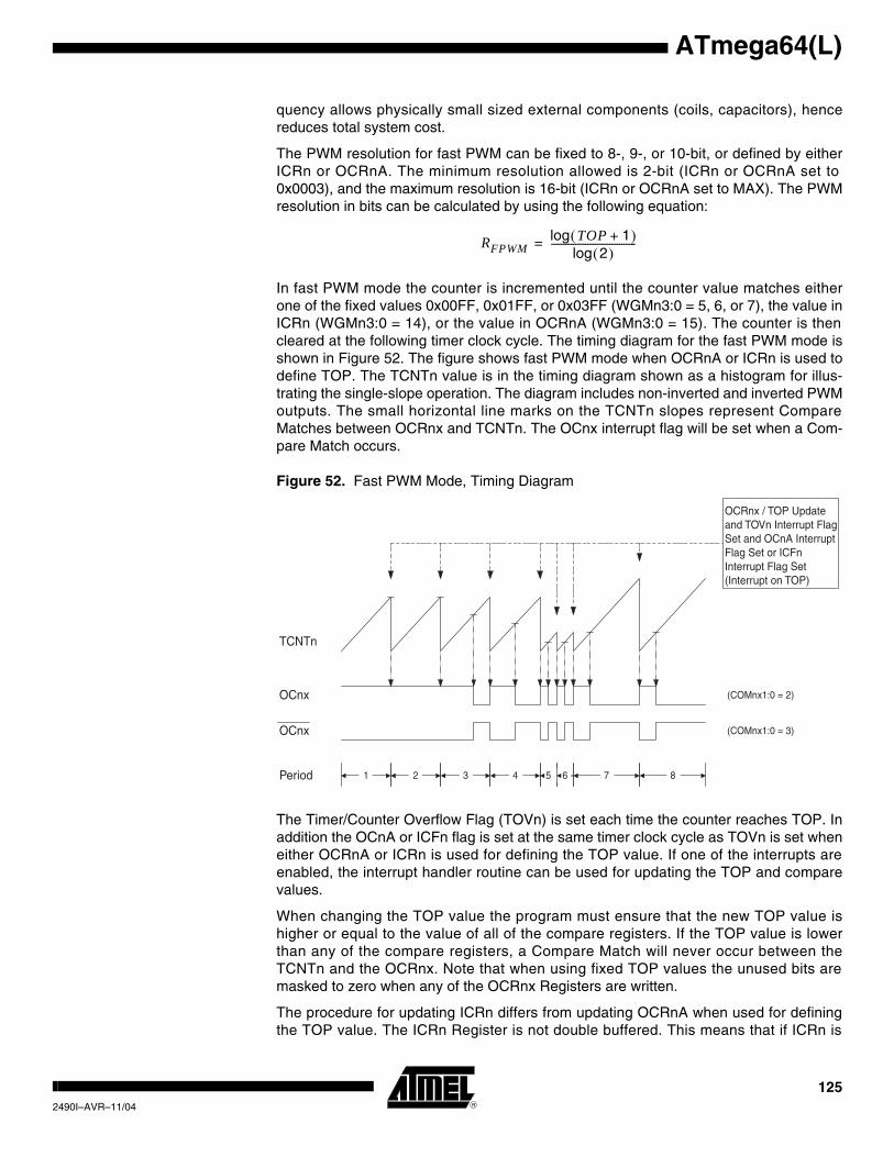
ATmega64(L)
quency allows physically small sized external components (coils, capacitors), hencereduces total system cost.
The PWM resolution for fast PWM can be fixed to 8-, 9-, or 10-bit, or defined by eitherICRn or OCRnA. The minimum resolution allowed is 2-bit (ICRn or OCRnA set to0x0003), and the maximum resolution is 16-bit (ICRn or OCRnA set to MAX). The PWMresolution in bits can be calculated by using the following equation:
In fast PWM mode the counter is incremented until the counter value matches eitherone of the fixed values 0x00FF, 0x01FF, or 0x03FF (WGMn3:0 = 5, 6, or 7), the value inICRn (WGMn3:0 = 14), or the value in OCRnA (WGMn3:0 = 15). The counter is thencleared at the following timer clock cycle. The timing diagram for the fast PWM mode isshown in Figure 52. The figure shows fast PWM mode when OCRnA or ICRn is used todefine TOP. The TCNTn value is in the timing diagram shown as a histogram for illus-trating the single-slope operation. The diagram includes non-inverted and inverted PWMoutputs. The small horizontal line marks on the TCNTn slopes represent CompareMatches between OCRnx and TCNTn. The OCnx interrupt flag will be set when a Com-pare Match occurs.
Figure 52. Fast PWM Mode, Timing Diagram
The Timer/Counter Overflow Flag (TOVn) is set each time the counter reaches TOP. Inaddition the OCnA or ICFn flag is set at the same timer clock cycle as TOVn is set wheneither OCRnA or ICRn is used for defining the TOP value. If one of the interrupts areenabled, the interrupt handler routine can be used for updating the TOP and comparevalues.
When changing the TOP value the program must ensure that the new TOP value ishigher or equal to the value of all of the compare registers. If the TOP value is lowerthan any of the compare registers, a Compare Match will never occur between theTCNTn and the OCRnx. Note that when using fixed TOP values the unused bits aremasked to zero when any of the OCRnx Registers are written.
The procedure for updating ICRn differs from updating OCRnA when used for definingthe TOP value. The ICRn Register is not double buffered. This means that if ICRn is
RFPWMTOP 1+( )log
2( )log-----------------------------------=
TCNTn
OCRnx / TOP Update and TOVn Interrupt Flag Set and OCnA Interrupt Flag Set or ICFn Interrupt Flag Set (Interrupt on TOP)
1 7Period 2 3 4 5 6 8
OCnx
OCnx
(COMnx1:0 = 2)
(COMnx1:0 = 3)
1252490I–AVR–11/04
changed to a low value when the counter is running with none or a low prescaler value,there is a risk that the new ICRn value written is lower than the current value of TCNTn.The result will then be that the counter will miss the Compare Match at the TOP value.The counter will then have to count to the MAX value (0xFFFF) and wrap around start-ing at 0x0000 before the Compare Match can occur. The OCRnA Register however, isdouble buffered. This feature allows the OCRnA I/O location to be written anytime.When the OCRnA I/O location is written the value written will be put into the OCRnABuffer Register. The OCRnA Compare Register will then be updated with the value inthe buffer register at the next timer clock cycle the TCNTn matches TOP. The update isdone at the same timer clock cycle as the TCNTn is cleared and the TOVn flag is set.
Using the ICRn Register for defining TOP works well when using fixed TOP values. Byusing ICRn, the OCRnA Register is free to be used for generating a PWM output onOCnA. However, if the base PWM frequency is actively changed (by changing the TOPvalue), using the OCRnA as TOP is clearly a better choice due to its double bufferfeature.
In fast PWM mode, the compare units allow generation of PWM waveforms on theOCnx pins. Setting the COMnx1:0 bits to two will produce a non-inverted PWM and aninverted PWM output can be generated by setting the COMnx1:0 to three (See Table 59on page 133). The actual OCnx value will only be visible on the port pin if the data direc-tion for the port pin is set as output (DDR_OCnx). The PWM waveform is generated bysetting (or clearing) the OCnx Register at the Compare Match between OCRnx andTCNTn, and clearing (or setting) the OCnx Register at the timer clock cycle the counteris cleared (changes from TOP to BOTTOM).
The PWM frequency for the output can be calculated by the following equation:
The N variable represents the prescaler divider (1, 8, 64, 256, or 1024).
The extreme values for the OCRnx Register represents special cases when generatinga PWM waveform output in the fast PWM mode. If the OCRnx is set equal to BOTTOM(0x0000) the output will be a narrow spike for each TOP+1 timer clock cycle. Setting theOCRnx equal to TOP will result in a constant high or low output (depending on the polar-ity of the output set by the COMnx1:0 bits.)
A frequency (with 50% duty cycle) waveform output in fast PWM mode can be achievedby setting OCnA to toggle its logical level on each Compare Match (COMnA1:0 = 1).This applies only if OCRnA is used to define the TOP value (WGMn3:0 = 15). The wave-form generated will have a maximum frequency of fOCnA = fclk_I/O/2 when OCRnA is set tozero (0x0000). This feature is similar to the OCnA toggle in CTC mode, except the dou-ble buffer feature of the Output Compare unit is enabled in the fast PWM mode.
Phase Correct PWM Mode The phase correct Pulse Width Modulation or phase correct PWM mode (WGMn3:0 = 1,2, 3, 10, or 11) provides a high resolution phase correct PWM waveform generationoption. The phase correct PWM mode is, like the phase and frequency correct PWMmode, based on a dual-slope operation. The counter counts repeatedly from BOTTOM(0x0000) to TOP and then from TOP to BOTTOM. In non-inverting Compare Outputmode, the Output Compare (OCnx) is cleared on the Compare Match between TCNTnand OCRnx while upcounting, and set on the Compare Match while downcounting. Ininverting Output Compare mode, the operation is inverted. The dual-slope operation haslower maximum operation frequency than single slope operation. However, due to thesymmetric feature of the dual-slope PWM modes, these modes are preferred for motorcontrol applications.
fOCnxPWMfclk_I/O
N 1 TOP+( )⋅-----------------------------------=
126 ATmega64(L)2490I–AVR–11/04
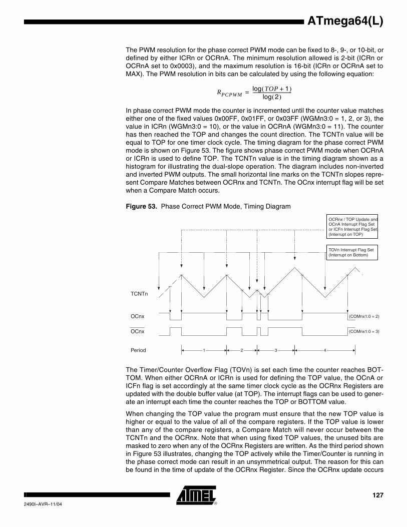
ATmega64(L)
The PWM resolution for the phase correct PWM mode can be fixed to 8-, 9-, or 10-bit, ordefined by either ICRn or OCRnA. The minimum resolution allowed is 2-bit (ICRn orOCRnA set to 0x0003), and the maximum resolution is 16-bit (ICRn or OCRnA set toMAX). The PWM resolution in bits can be calculated by using the following equation:
In phase correct PWM mode the counter is incremented until the counter value matcheseither one of the fixed values 0x00FF, 0x01FF, or 0x03FF (WGMn3:0 = 1, 2, or 3), thevalue in ICRn (WGMn3:0 = 10), or the value in OCRnA (WGMn3:0 = 11). The counterhas then reached the TOP and changes the count direction. The TCNTn value will beequal to TOP for one timer clock cycle. The timing diagram for the phase correct PWMmode is shown on Figure 53. The figure shows phase correct PWM mode when OCRnAor ICRn is used to define TOP. The TCNTn value is in the timing diagram shown as ahistogram for illustrating the dual-slope operation. The diagram includes non-invertedand inverted PWM outputs. The small horizontal line marks on the TCNTn slopes repre-sent Compare Matches between OCRnx and TCNTn. The OCnx interrupt flag will be setwhen a Compare Match occurs.
Figure 53. Phase Correct PWM Mode, Timing Diagram
The Timer/Counter Overflow Flag (TOVn) is set each time the counter reaches BOT-TOM. When either OCRnA or ICRn is used for defining the TOP value, the OCnA orICFn flag is set accordingly at the same timer clock cycle as the OCRnx Registers areupdated with the double buffer value (at TOP). The interrupt flags can be used to gener-ate an interrupt each time the counter reaches the TOP or BOTTOM value.
When changing the TOP value the program must ensure that the new TOP value ishigher or equal to the value of all of the compare registers. If the TOP value is lowerthan any of the compare registers, a Compare Match will never occur between theTCNTn and the OCRnx. Note that when using fixed TOP values, the unused bits aremasked to zero when any of the OCRnx Registers are written. As the third period shownin Figure 53 illustrates, changing the TOP actively while the Timer/Counter is running inthe phase correct mode can result in an unsymmetrical output. The reason for this canbe found in the time of update of the OCRnx Register. Since the OCRnx update occurs
RPCPWMTOP 1+( )log
2( )log-----------------------------------=
OCRnx / TOP Update andOCnA Interrupt Flag Setor ICFn Interrupt Flag Set(Interrupt on TOP)
1 2 3 4
TOVn Interrupt Flag Set(Interrupt on Bottom)
TCNTn
Period
OCnx
OCnx
(COMnx1:0 = 2)
(COMnx1:0 = 3)
1272490I–AVR–11/04
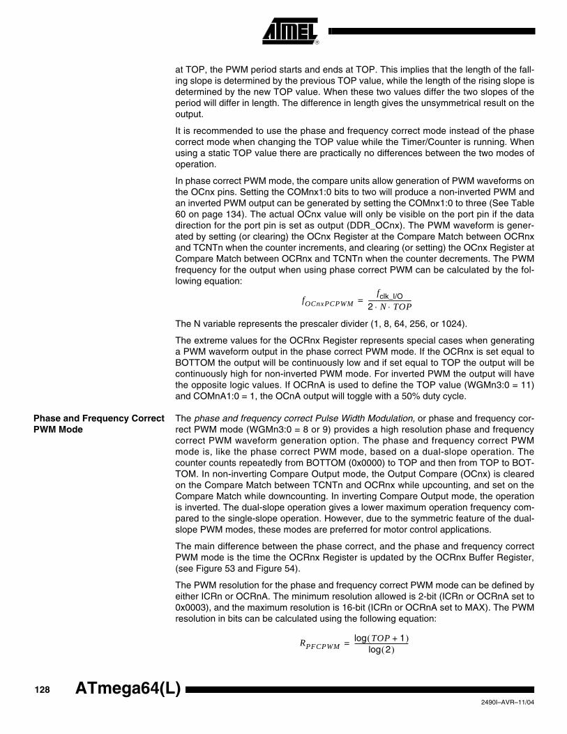
at TOP, the PWM period starts and ends at TOP. This implies that the length of the fall-ing slope is determined by the previous TOP value, while the length of the rising slope isdetermined by the new TOP value. When these two values differ the two slopes of theperiod will differ in length. The difference in length gives the unsymmetrical result on theoutput.
It is recommended to use the phase and frequency correct mode instead of the phasecorrect mode when changing the TOP value while the Timer/Counter is running. Whenusing a static TOP value there are practically no differences between the two modes ofoperation.
In phase correct PWM mode, the compare units allow generation of PWM waveforms onthe OCnx pins. Setting the COMnx1:0 bits to two will produce a non-inverted PWM andan inverted PWM output can be generated by setting the COMnx1:0 to three (See Table60 on page 134). The actual OCnx value will only be visible on the port pin if the datadirection for the port pin is set as output (DDR_OCnx). The PWM waveform is gener-ated by setting (or clearing) the OCnx Register at the Compare Match between OCRnxand TCNTn when the counter increments, and clearing (or setting) the OCnx Register atCompare Match between OCRnx and TCNTn when the counter decrements. The PWMfrequency for the output when using phase correct PWM can be calculated by the fol-lowing equation:
The N variable represents the prescaler divider (1, 8, 64, 256, or 1024).
The extreme values for the OCRnx Register represents special cases when generatinga PWM waveform output in the phase correct PWM mode. If the OCRnx is set equal toBOTTOM the output will be continuously low and if set equal to TOP the output will becontinuously high for non-inverted PWM mode. For inverted PWM the output will havethe opposite logic values. If OCRnA is used to define the TOP value (WGMn3:0 = 11)and COMnA1:0 = 1, the OCnA output will toggle with a 50% duty cycle.
Phase and Frequency Correct PWM Mode
The phase and frequency correct Pulse Width Modulation, or phase and frequency cor-rect PWM mode (WGMn3:0 = 8 or 9) provides a high resolution phase and frequencycorrect PWM waveform generation option. The phase and frequency correct PWMmode is, like the phase correct PWM mode, based on a dual-slope operation. Thecounter counts repeatedly from BOTTOM (0x0000) to TOP and then from TOP to BOT-TOM. In non-inverting Compare Output mode, the Output Compare (OCnx) is clearedon the Compare Match between TCNTn and OCRnx while upcounting, and set on theCompare Match while downcounting. In inverting Compare Output mode, the operationis inverted. The dual-slope operation gives a lower maximum operation frequency com-pared to the single-slope operation. However, due to the symmetric feature of the dual-slope PWM modes, these modes are preferred for motor control applications.
The main difference between the phase correct, and the phase and frequency correctPWM mode is the time the OCRnx Register is updated by the OCRnx Buffer Register,(see Figure 53 and Figure 54).
The PWM resolution for the phase and frequency correct PWM mode can be defined byeither ICRn or OCRnA. The minimum resolution allowed is 2-bit (ICRn or OCRnA set to0x0003), and the maximum resolution is 16-bit (ICRn or OCRnA set to MAX). The PWMresolution in bits can be calculated using the following equation:
fOCnxPCPWMfclk_I/O
2 N TOP⋅ ⋅----------------------------=
RPFCPWMTOP 1+( )log
2( )log-----------------------------------=
128 ATmega64(L)2490I–AVR–11/04
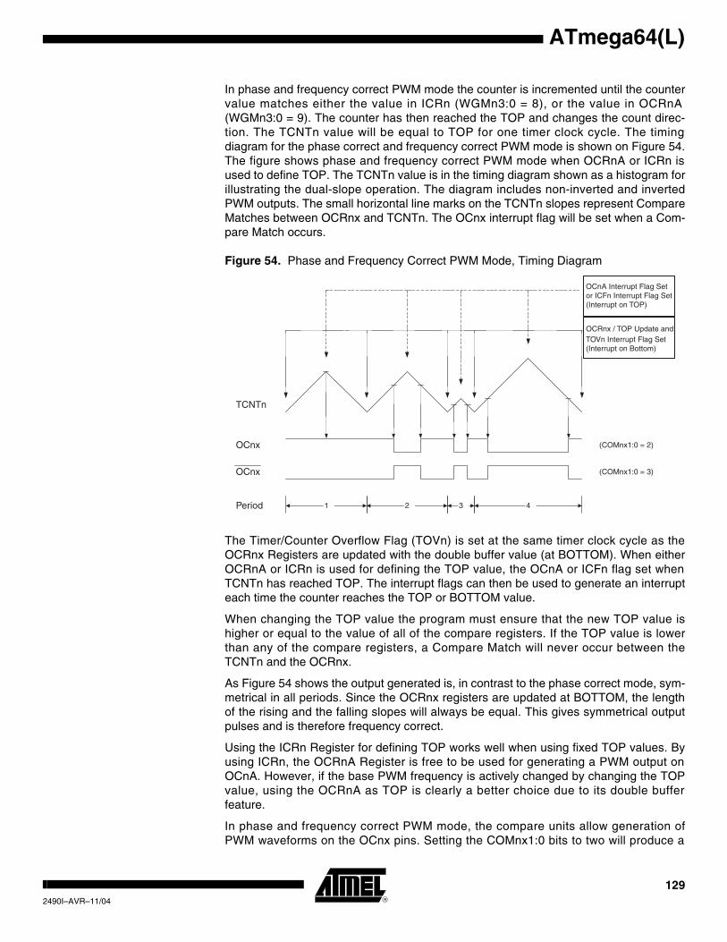
ATmega64(L)
In phase and frequency correct PWM mode the counter is incremented until the countervalue matches either the value in ICRn (WGMn3:0 = 8), or the value in OCRnA(WGMn3:0 = 9). The counter has then reached the TOP and changes the count direc-tion. The TCNTn value will be equal to TOP for one timer clock cycle. The timingdiagram for the phase correct and frequency correct PWM mode is shown on Figure 54.The figure shows phase and frequency correct PWM mode when OCRnA or ICRn isused to define TOP. The TCNTn value is in the timing diagram shown as a histogram forillustrating the dual-slope operation. The diagram includes non-inverted and invertedPWM outputs. The small horizontal line marks on the TCNTn slopes represent CompareMatches between OCRnx and TCNTn. The OCnx interrupt flag will be set when a Com-pare Match occurs.
Figure 54. Phase and Frequency Correct PWM Mode, Timing Diagram
The Timer/Counter Overflow Flag (TOVn) is set at the same timer clock cycle as theOCRnx Registers are updated with the double buffer value (at BOTTOM). When eitherOCRnA or ICRn is used for defining the TOP value, the OCnA or ICFn flag set whenTCNTn has reached TOP. The interrupt flags can then be used to generate an interrupteach time the counter reaches the TOP or BOTTOM value.
When changing the TOP value the program must ensure that the new TOP value ishigher or equal to the value of all of the compare registers. If the TOP value is lowerthan any of the compare registers, a Compare Match will never occur between theTCNTn and the OCRnx.
As Figure 54 shows the output generated is, in contrast to the phase correct mode, sym-metrical in all periods. Since the OCRnx registers are updated at BOTTOM, the lengthof the rising and the falling slopes will always be equal. This gives symmetrical outputpulses and is therefore frequency correct.
Using the ICRn Register for defining TOP works well when using fixed TOP values. Byusing ICRn, the OCRnA Register is free to be used for generating a PWM output onOCnA. However, if the base PWM frequency is actively changed by changing the TOPvalue, using the OCRnA as TOP is clearly a better choice due to its double bufferfeature.
In phase and frequency correct PWM mode, the compare units allow generation ofPWM waveforms on the OCnx pins. Setting the COMnx1:0 bits to two will produce a
OCRnx / TOP Update andTOVn Interrupt Flag Set(Interrupt on Bottom)
OCnA Interrupt Flag Setor ICFn Interrupt Flag Set(Interrupt on TOP)
1 2 3 4
TCNTn
Period
OCnx
OCnx
(COMnx1:0 = 2)
(COMnx1:0 = 3)
1292490I–AVR–11/04
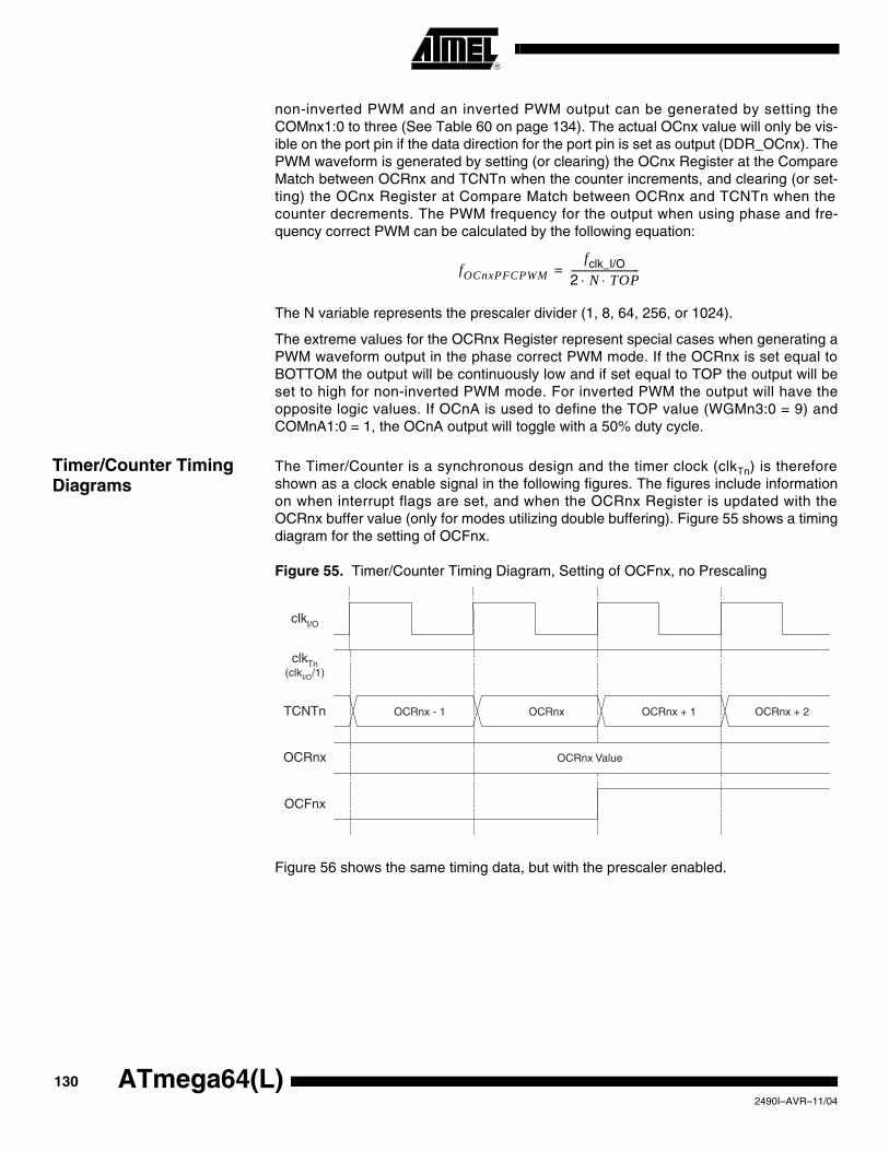
non-inverted PWM and an inverted PWM output can be generated by setting theCOMnx1:0 to three (See Table 60 on page 134). The actual OCnx value will only be vis-ible on the port pin if the data direction for the port pin is set as output (DDR_OCnx). ThePWM waveform is generated by setting (or clearing) the OCnx Register at the CompareMatch between OCRnx and TCNTn when the counter increments, and clearing (or set-ting) the OCnx Register at Compare Match between OCRnx and TCNTn when thecounter decrements. The PWM frequency for the output when using phase and fre-quency correct PWM can be calculated by the following equation:
The N variable represents the prescaler divider (1, 8, 64, 256, or 1024).
The extreme values for the OCRnx Register represent special cases when generating aPWM waveform output in the phase correct PWM mode. If the OCRnx is set equal toBOTTOM the output will be continuously low and if set equal to TOP the output will beset to high for non-inverted PWM mode. For inverted PWM the output will have theopposite logic values. If OCnA is used to define the TOP value (WGMn3:0 = 9) andCOMnA1:0 = 1, the OCnA output will toggle with a 50% duty cycle.
Timer/Counter Timing Diagrams
The Timer/Counter is a synchronous design and the timer clock (clkTn) is thereforeshown as a clock enable signal in the following figures. The figures include informationon when interrupt flags are set, and when the OCRnx Register is updated with theOCRnx buffer value (only for modes utilizing double buffering). Figure 55 shows a timingdiagram for the setting of OCFnx.
Figure 55. Timer/Counter Timing Diagram, Setting of OCFnx, no Prescaling
Figure 56 shows the same timing data, but with the prescaler enabled.
fOCnxPFCPWMfclk_I/O
2 N TOP⋅ ⋅----------------------------=
clkTn(clkI/O/1)
OCFnx
clkI/O
OCRnx
TCNTn
OCRnx Value
OCRnx - 1 OCRnx OCRnx + 1 OCRnx + 2
130 ATmega64(L)2490I–AVR–11/04
ATmega64(L)
Figure 56. Timer/Counter Timing Diagram, Setting of OCFnx, with Prescaler (fclk_I/O/8)
Figure 57 shows the count sequence close to TOP in various modes. When using phaseand frequency correct PWM mode the OCRnx Register is updated at BOTTOM. Thetiming diagrams will be the same, but TOP should be replaced by BOTTOM, TOP-1 byBOTTOM+1 and so on. The same renaming applies for modes that set the TOVn flag atBOTTOM.
Figure 57. Timer/Counter Timing Diagram, no Prescaling
Figure 58 shows the same timing data, but with the prescaler enabled.
OCFnx
OCRnx
TCNTn
OCRnx Value
OCRnx - 1 OCRnx OCRnx + 1 OCRnx + 2
clkI/O
clkTn(clkI/O/8)
TOVn (FPWM)and ICFn (if used
as TOP)
OCRnx(Update at TOP)
TCNTn(CTC and FPWM)
TCNTn(PC and PFC PWM)
TOP - 1 TOP TOP - 1 TOP - 2
Old OCRnx Value New OCRnx Value
TOP - 1 TOP BOTTOM BOTTOM + 1
clkTn(clkI/O/1)
clkI/O
1312490I–AVR–11/04
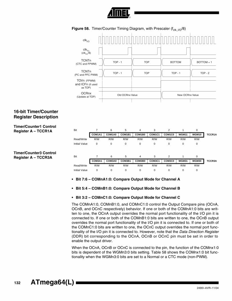
Figure 58. Timer/Counter Timing Diagram, with Prescaler (fclk_I/O/8)
16-bit Timer/Counter Register Description
Timer/Counter1 Control Register A – TCCR1A
Timer/Counter3 Control Register A – TCCR3A
• Bit 7:6 – COMnA1:0: Compare Output Mode for Channel A
• Bit 5:4 – COMnB1:0: Compare Output Mode for Channel B
• Bit 3:2 – COMnC1:0: Compare Output Mode for Channel C
The COMnA1:0, COMnB1:0, and COMnC1:0 control the Output Compare pins (OCnA,OCnB, and OCnC respectively) behavior. If one or both of the COMnA1:0 bits are writ-ten to one, the OCnA output overrides the normal port functionality of the I/O pin it isconnected to. If one or both of the COMnB1:0 bits are written to one, the OCnB outputoverrides the normal port functionality of the I/O pin it is connected to. If one or both ofthe COMnC1:0 bits are written to one, the OCnC output overrides the normal port func-tionality of the I/O pin it is connected to. However, note that the Data Direction Register(DDR) bit corresponding to the OCnA, OCnB or OCnC pin must be set in order toenable the output driver.
When the OCnA, OCnB or OCnC is connected to the pin, the function of the COMnx1:0bits is dependent of the WGMn3:0 bits setting. Table 58 shows the COMnx1:0 bit func-tionality when the WGMn3:0 bits are set to a Normal or a CTC mode (non-PWM).
TOVn (FPWM)and ICFn (if used
as TOP)
OCRnx(Update at TOP)
TCNTn(CTC and FPWM)
TCNTn(PC and PFC PWM)
TOP - 1 TOP TOP - 1 TOP - 2
Old OCRnx Value New OCRnx Value
TOP - 1 TOP BOTTOM BOTTOM + 1
clkI/O
clkTn(clkI/O/8)
Bit 7 6 5 4 3 2 1 0
COM1A1 COM1A0 COM1B1 COM1B0 COM1C1 COM1C0 WGM11 WGM10 TCCR1A
Read/Write R/W R/W R/W R/W R/W R/W R/W R/W
Initial Value 0 0 0 0 0 0 0 0
Bit 7 6 5 4 3 2 1 0
COM3A1 COM3A0 COM3B1 COM3B0 COM3C1 COM3C0 WGM31 WGM30 TCCR3A
Read/Write R/W R/W R/W R/W R/W R/W R/W R/W
Initial Value 0 0 0 0 0 0 0 0
132 ATmega64(L)2490I–AVR–11/04
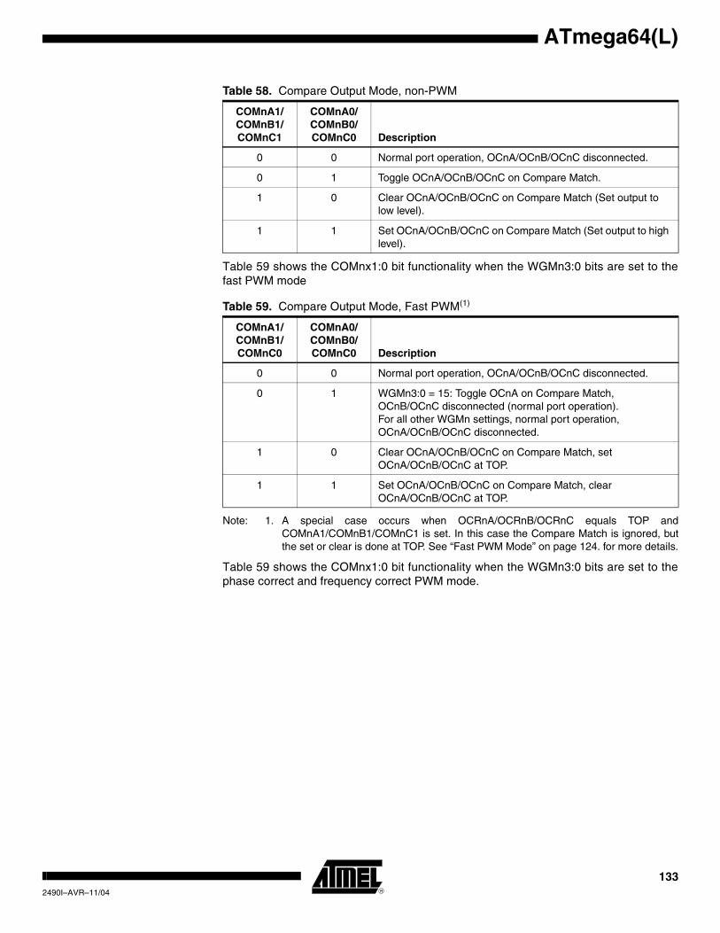
ATmega64(L)
Table 59 shows the COMnx1:0 bit functionality when the WGMn3:0 bits are set to thefast PWM mode
Note: 1. A special case occurs when OCRnA/OCRnB/OCRnC equals TOP andCOMnA1/COMnB1/COMnC1 is set. In this case the Compare Match is ignored, butthe set or clear is done at TOP. See “Fast PWM Mode” on page 124. for more details.
Table 59 shows the COMnx1:0 bit functionality when the WGMn3:0 bits are set to thephase correct and frequency correct PWM mode.
Table 58. Compare Output Mode, non-PWM
COMnA1/ COMnB1/ COMnC1
COMnA0/ COMnB0/ COMnC0 Description
0 0 Normal port operation, OCnA/OCnB/OCnC disconnected.
0 1 Toggle OCnA/OCnB/OCnC on Compare Match.
1 0 Clear OCnA/OCnB/OCnC on Compare Match (Set output to low level).
1 1 Set OCnA/OCnB/OCnC on Compare Match (Set output to high level).
Table 59. Compare Output Mode, Fast PWM(1)
COMnA1/ COMnB1/ COMnC0
COMnA0/ COMnB0/ COMnC0 Description
0 0 Normal port operation, OCnA/OCnB/OCnC disconnected.
0 1 WGMn3:0 = 15: Toggle OCnA on Compare Match, OCnB/OCnC disconnected (normal port operation).For all other WGMn settings, normal port operation, OCnA/OCnB/OCnC disconnected.
1 0 Clear OCnA/OCnB/OCnC on Compare Match, set OCnA/OCnB/OCnC at TOP.
1 1 Set OCnA/OCnB/OCnC on Compare Match, clear OCnA/OCnB/OCnC at TOP.
1332490I–AVR–11/04
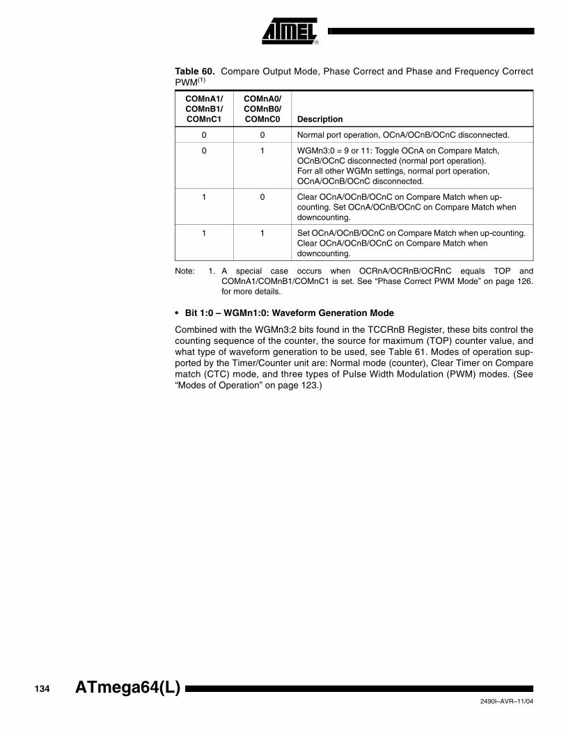
Note: 1. A special case occurs when OCRnA/OCRnB/OCRnC equals TOP andCOMnA1/COMnB1/COMnC1 is set. See “Phase Correct PWM Mode” on page 126.for more details.
• Bit 1:0 – WGMn1:0: Waveform Generation Mode
Combined with the WGMn3:2 bits found in the TCCRnB Register, these bits control thecounting sequence of the counter, the source for maximum (TOP) counter value, andwhat type of waveform generation to be used, see Table 61. Modes of operation sup-ported by the Timer/Counter unit are: Normal mode (counter), Clear Timer on Comparematch (CTC) mode, and three types of Pulse Width Modulation (PWM) modes. (See“Modes of Operation” on page 123.)
Table 60. Compare Output Mode, Phase Correct and Phase and Frequency CorrectPWM(1)
COMnA1/ COMnB1/ COMnC1
COMnA0/ COMnB0/ COMnC0 Description
0 0 Normal port operation, OCnA/OCnB/OCnC disconnected.
0 1 WGMn3:0 = 9 or 11: Toggle OCnA on Compare Match, OCnB/OCnC disconnected (normal port operation).Forr all other WGMn settings, normal port operation, OCnA/OCnB/OCnC disconnected.
1 0 Clear OCnA/OCnB/OCnC on Compare Match when up-counting. Set OCnA/OCnB/OCnC on Compare Match when downcounting.
1 1 Set OCnA/OCnB/OCnC on Compare Match when up-counting. Clear OCnA/OCnB/OCnC on Compare Match when downcounting.
134 ATmega64(L)2490I–AVR–11/04
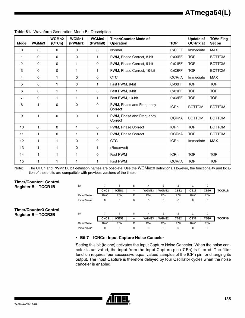
ATmega64(L)
Note: The CTCn and PWMn1:0 bit definition names are obsolete. Use the WGMn2:0 definitions. However, the functionality and loca-tion of these bits are compatible with previous versions of the timer.
Timer/Counter1 Control Register B – TCCR1B
Timer/Counter3 Control Register B – TCCR3B
• Bit 7 – ICNCn: Input Capture Noise Canceler
Setting this bit (to one) activates the Input Capture Noise Canceler. When the noise can-celer is activated, the input from the Input Capture pin (ICPn) is filtered. The filterfunction requires four successive equal valued samples of the ICPn pin for changing itsoutput. The Input Capture is therefore delayed by four Oscillator cycles when the noisecanceler is enabled.
Table 61. Waveform Generation Mode Bit Description
Mode WGMn3WGMn2(CTCn)
WGMn1(PWMn1)
WGMn0(PWMn0)
Timer/Counter Mode of Operation TOP
Update ofOCRnx at
TOVn FlagSet on
0 0 0 0 0 Normal 0xFFFF Immediate MAX
1 0 0 0 1 PWM, Phase Correct, 8-bit 0x00FF TOP BOTTOM
2 0 0 1 0 PWM, Phase Correct, 9-bit 0x01FF TOP BOTTOM
3 0 0 1 1 PWM, Phase Correct, 10-bit 0x03FF TOP BOTTOM
4 0 1 0 0 CTC OCRnA Immediate MAX
5 0 1 0 1 Fast PWM, 8-bit 0x00FF TOP TOP
6 0 1 1 0 Fast PWM, 9-bit 0x01FF TOP TOP
7 0 1 1 1 Fast PWM, 10-bit 0x03FF TOP TOP
8 1 0 0 0 PWM, Phase and Frequency Correct
ICRn BOTTOM BOTTOM
9 1 0 0 1 PWM, Phase and Frequency Correct
OCRnA BOTTOM BOTTOM
10 1 0 1 0 PWM, Phase Correct ICRn TOP BOTTOM
11 1 0 1 1 PWM, Phase Correct OCRnA TOP BOTTOM
12 1 1 0 0 CTC ICRn Immediate MAX
13 1 1 0 1 (Reserved) – – –
14 1 1 1 0 Fast PWM ICRn TOP TOP
15 1 1 1 1 Fast PWM OCRnA TOP TOP
Bit 7 6 5 4 3 2 1 0
ICNC1 ICES1 – WGM13 WGM12 CS12 CS11 CS10 TCCR1BRead/Write R/W R/W R R/W R/W R/W R/W R/W
Initial Value 0 0 0 0 0 0 0 0
Bit 7 6 5 4 3 2 1 0
ICNC3 ICES3 – WGM33 WGM32 CS32 CS31 CS30 TCCR3BRead/Write R/W R/W R R/W R/W R/W R/W R/W
Initial Value 0 0 0 0 0 0 0 0
1352490I–AVR–11/04
• Bit 6 – ICESn: Input Capture Edge Select
This bit selects which edge on the Input Capture pin (ICPn) that is used to trigger a cap-ture event. When the ICESn bit is written to zero, a falling (negative) edge is used astrigger, and when the ICESn bit is written to one, a rising (positive) edge will trigger thecapture.
When a capture is triggered according to the ICESn setting, the counter value is copiedinto the Input Capture Register (ICRn). The event will also set the Input Capture Flag(ICFn), and this can be used to cause an Input Capture Interrupt, if this interrupt isenabled.
When the ICRn is used as TOP value (see description of the WGMn3:0 bits located inthe TCCRnA and the TCCRnB Register), the ICPn is disconnected and consequentlythe Input Capture function is disabled.
• Bit 5 – Reserved Bit
This bit is reserved for future use. For ensuring compatibility with future devices, this bitmust be written to zero when TCCRnB is written.
• Bit 4:3 – WGMn3:2: Waveform Generation Mode
See TCCRnA Register description.
• Bit 2:0 – CSn2:0: Clock Select
The three Clock Select bits select the clock source to be used by the Timer/Counter, seeFigure 55 and Figure 56.
If external pin modes are used for the Timer/Countern, transitions on the Tn pin willclock the counter even if the pin is configured as an output. This feature allows softwarecontrol of the counting.
Timer/Counter1 Control Register C – TCCR1C
Table 62. Clock Select Bit Description
CSn2 CSn1 CSn0 Description
0 0 0 No clock source (Timer/counter stopped).
0 0 1 clkI/O/1 (No prescaling)
0 1 0 clkI/O/8 (From prescaler)
0 1 1 clkI/O/64 (From prescaler)
1 0 0 clkI/O/256 (From prescaler)
1 0 1 clkI/O/1024 (From prescaler)
1 1 0 External clock source on Tn pin. Clock on falling edge.
1 1 1 External clock source on Tn pin. Clock on rising edge.
Bit 7 6 5 4 3 2 1 0
FOC1A FOC1B FOC1C – – – – – TCCR1CRead/Write W W W R R R R R
Initial Value 0 0 0 0 0 0 0 0
136 ATmega64(L)2490I–AVR–11/04
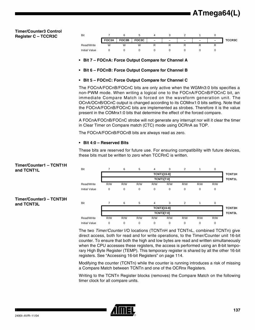
ATmega64(L)
Timer/Counter3 Control Register C – TCCR3C
• Bit 7 – FOCnA: Force Output Compare for Channel A
• Bit 6 – FOCnB: Force Output Compare for Channel B
• Bit 5 – FOCnC: Force Output Compare for Channel C
The FOCnA/FOCnB/FOCnC bits are only active when the WGMn3:0 bits specifies anon-PWM mode. When writing a logical one to the FOCnA/FOCnB/FOCnC bit, animmediate Compare Match is forced on the waveform generation unit. TheOCnA/OCnB/OCnC output is changed according to its COMnx1:0 bits setting. Note thatthe FOCnA/FOCnB/FOCnC bits are implemented as strobes. Therefore it is the valuepresent in the COMnx1:0 bits that determine the effect of the forced compare.
A FOCnA/FOCnB/FOCnC strobe will not generate any interrupt nor will it clear the timerin Clear Timer on Compare match (CTC) mode using OCRnA as TOP.
The FOCnA/FOCnB/FOCnB bits are always read as zero.
• Bit 4:0 – Reserved Bits
These bits are reserved for future use. For ensuring compatibility with future devices,these bits must be written to zero when TCCRnC is written.
Timer/Counter1 – TCNT1H and TCNT1L
Timer/Counter3 – TCNT3H and TCNT3L
The two Timer/Counter I/O locations (TCNTnH and TCNTnL, combined TCNTn) givedirect access, both for read and for write operations, to the Timer/Counter unit 16-bitcounter. To ensure that both the high and low bytes are read and written simultaneouslywhen the CPU accesses these registers, the access is performed using an 8-bit tempo-rary High Byte Register (TEMP). This temporary register is shared by all the other 16-bitregisters. See “Accessing 16-bit Registers” on page 114.
Modifying the counter (TCNTn) while the counter is running introduces a risk of missinga Compare Match between TCNTn and one of the OCRnx Registers.
Writing to the TCNTn Register blocks (removes) the Compare Match on the followingtimer clock for all compare units.
Bit 7 6 5 4 3 2 1 0
FOC3A FOC3B FOC3C – – – – – TCCR3CRead/Write W W W R R R R R
Initial Value 0 0 0 0 0 0 0 0
Bit 7 6 5 4 3 2 1 0
TCNT1[15:8] TCNT1HTCNT1[7:0] TCNT1L
Read/Write R/W R/W R/W R/W R/W R/W R/W R/W
Initial Value 0 0 0 0 0 0 0 0
Bit 7 6 5 4 3 2 1 0
TCNT3[15:8] TCNT3HTCNT3[7:0] TCNT3L
Read/Write R/W R/W R/W R/W R/W R/W R/W R/W
Initial Value 0 0 0 0 0 0 0 0
1372490I–AVR–11/04
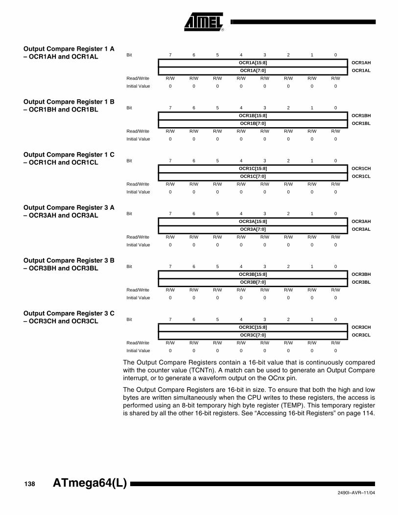
Output Compare Register 1 A – OCR1AH and OCR1AL
Output Compare Register 1 B – OCR1BH and OCR1BL
Output Compare Register 1 C – OCR1CH and OCR1CL
Output Compare Register 3 A – OCR3AH and OCR3AL
Output Compare Register 3 B – OCR3BH and OCR3BL
Output Compare Register 3 C – OCR3CH and OCR3CL
The Output Compare Registers contain a 16-bit value that is continuously comparedwith the counter value (TCNTn). A match can be used to generate an Output Compareinterrupt, or to generate a waveform output on the OCnx pin.
The Output Compare Registers are 16-bit in size. To ensure that both the high and lowbytes are written simultaneously when the CPU writes to these registers, the access isperformed using an 8-bit temporary high byte register (TEMP). This temporary registeris shared by all the other 16-bit registers. See “Accessing 16-bit Registers” on page 114.
Bit 7 6 5 4 3 2 1 0
OCR1A[15:8] OCR1AHOCR1A[7:0] OCR1AL
Read/Write R/W R/W R/W R/W R/W R/W R/W R/W
Initial Value 0 0 0 0 0 0 0 0
Bit 7 6 5 4 3 2 1 0
OCR1B[15:8] OCR1BHOCR1B[7:0] OCR1BL
Read/Write R/W R/W R/W R/W R/W R/W R/W R/W
Initial Value 0 0 0 0 0 0 0 0
Bit 7 6 5 4 3 2 1 0
OCR1C[15:8] OCR1CHOCR1C[7:0] OCR1CL
Read/Write R/W R/W R/W R/W R/W R/W R/W R/W
Initial Value 0 0 0 0 0 0 0 0
Bit 7 6 5 4 3 2 1 0
OCR3A[15:8] OCR3AHOCR3A[7:0] OCR3AL
Read/Write R/W R/W R/W R/W R/W R/W R/W R/W
Initial Value 0 0 0 0 0 0 0 0
Bit 7 6 5 4 3 2 1 0
OCR3B[15:8] OCR3BHOCR3B[7:0] OCR3BL
Read/Write R/W R/W R/W R/W R/W R/W R/W R/W
Initial Value 0 0 0 0 0 0 0 0
Bit 7 6 5 4 3 2 1 0
OCR3C[15:8] OCR3CHOCR3C[7:0] OCR3CL
Read/Write R/W R/W R/W R/W R/W R/W R/W R/W
Initial Value 0 0 0 0 0 0 0 0
138 ATmega64(L)2490I–AVR–11/04
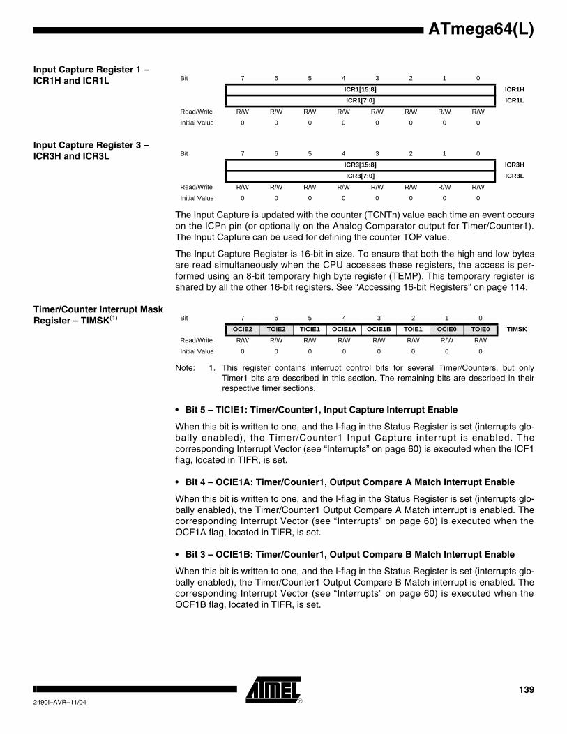
ATmega64(L)
Input Capture Register 1 – ICR1H and ICR1L
Input Capture Register 3 – ICR3H and ICR3L
The Input Capture is updated with the counter (TCNTn) value each time an event occurson the ICPn pin (or optionally on the Analog Comparator output for Timer/Counter1).The Input Capture can be used for defining the counter TOP value.
The Input Capture Register is 16-bit in size. To ensure that both the high and low bytesare read simultaneously when the CPU accesses these registers, the access is per-formed using an 8-bit temporary high byte register (TEMP). This temporary register isshared by all the other 16-bit registers. See “Accessing 16-bit Registers” on page 114.
Timer/Counter Interrupt Mask Register – TIMSK(1)
Note: 1. This register contains interrupt control bits for several Timer/Counters, but onlyTimer1 bits are described in this section. The remaining bits are described in theirrespective timer sections.
• Bit 5 – TICIE1: Timer/Counter1, Input Capture Interrupt Enable
When this bit is written to one, and the I-flag in the Status Register is set (interrupts glo-bally enabled), the Timer/Counter1 Input Capture interrupt is enabled. Thecorresponding Interrupt Vector (see “Interrupts” on page 60) is executed when the ICF1flag, located in TIFR, is set.
• Bit 4 – OCIE1A: Timer/Counter1, Output Compare A Match Interrupt Enable
When this bit is written to one, and the I-flag in the Status Register is set (interrupts glo-bally enabled), the Timer/Counter1 Output Compare A Match interrupt is enabled. Thecorresponding Interrupt Vector (see “Interrupts” on page 60) is executed when theOCF1A flag, located in TIFR, is set.
• Bit 3 – OCIE1B: Timer/Counter1, Output Compare B Match Interrupt Enable
When this bit is written to one, and the I-flag in the Status Register is set (interrupts glo-bally enabled), the Timer/Counter1 Output Compare B Match interrupt is enabled. Thecorresponding Interrupt Vector (see “Interrupts” on page 60) is executed when theOCF1B flag, located in TIFR, is set.
Bit 7 6 5 4 3 2 1 0
ICR1[15:8] ICR1HICR1[7:0] ICR1L
Read/Write R/W R/W R/W R/W R/W R/W R/W R/W
Initial Value 0 0 0 0 0 0 0 0
Bit 7 6 5 4 3 2 1 0
ICR3[15:8] ICR3HICR3[7:0] ICR3L
Read/Write R/W R/W R/W R/W R/W R/W R/W R/W
Initial Value 0 0 0 0 0 0 0 0
Bit 7 6 5 4 3 2 1 0
OCIE2 TOIE2 TICIE1 OCIE1A OCIE1B TOIE1 OCIE0 TOIE0 TIMSKRead/Write R/W R/W R/W R/W R/W R/W R/W R/W
Initial Value 0 0 0 0 0 0 0 0
1392490I–AVR–11/04
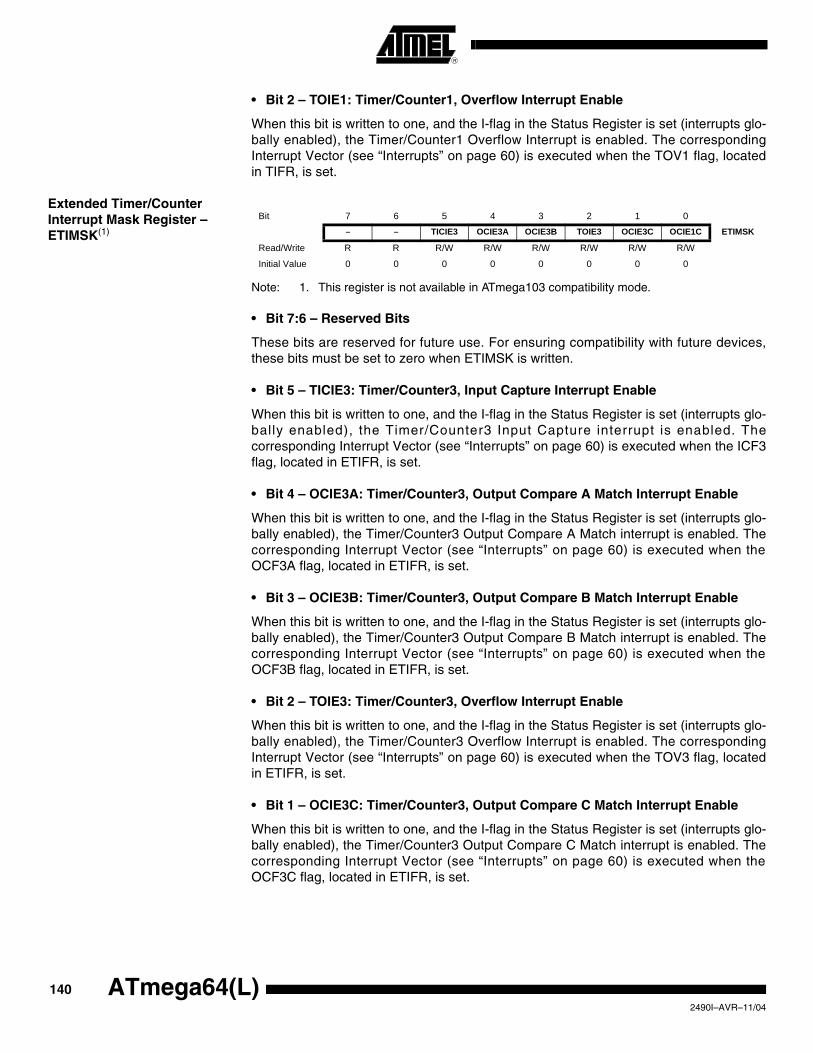
• Bit 2 – TOIE1: Timer/Counter1, Overflow Interrupt Enable
When this bit is written to one, and the I-flag in the Status Register is set (interrupts glo-bally enabled), the Timer/Counter1 Overflow Interrupt is enabled. The correspondingInterrupt Vector (see “Interrupts” on page 60) is executed when the TOV1 flag, locatedin TIFR, is set.
Extended Timer/Counter Interrupt Mask Register – ETIMSK(1)
Note: 1. This register is not available in ATmega103 compatibility mode.
• Bit 7:6 – Reserved Bits
These bits are reserved for future use. For ensuring compatibility with future devices,these bits must be set to zero when ETIMSK is written.
• Bit 5 – TICIE3: Timer/Counter3, Input Capture Interrupt Enable
When this bit is written to one, and the I-flag in the Status Register is set (interrupts glo-bally enabled), the Timer/Counter3 Input Capture interrupt is enabled. Thecorresponding Interrupt Vector (see “Interrupts” on page 60) is executed when the ICF3flag, located in ETIFR, is set.
• Bit 4 – OCIE3A: Timer/Counter3, Output Compare A Match Interrupt Enable
When this bit is written to one, and the I-flag in the Status Register is set (interrupts glo-bally enabled), the Timer/Counter3 Output Compare A Match interrupt is enabled. Thecorresponding Interrupt Vector (see “Interrupts” on page 60) is executed when theOCF3A flag, located in ETIFR, is set.
• Bit 3 – OCIE3B: Timer/Counter3, Output Compare B Match Interrupt Enable
When this bit is written to one, and the I-flag in the Status Register is set (interrupts glo-bally enabled), the Timer/Counter3 Output Compare B Match interrupt is enabled. Thecorresponding Interrupt Vector (see “Interrupts” on page 60) is executed when theOCF3B flag, located in ETIFR, is set.
• Bit 2 – TOIE3: Timer/Counter3, Overflow Interrupt Enable
When this bit is written to one, and the I-flag in the Status Register is set (interrupts glo-bally enabled), the Timer/Counter3 Overflow Interrupt is enabled. The correspondingInterrupt Vector (see “Interrupts” on page 60) is executed when the TOV3 flag, locatedin ETIFR, is set.
• Bit 1 – OCIE3C: Timer/Counter3, Output Compare C Match Interrupt Enable
When this bit is written to one, and the I-flag in the Status Register is set (interrupts glo-bally enabled), the Timer/Counter3 Output Compare C Match interrupt is enabled. Thecorresponding Interrupt Vector (see “Interrupts” on page 60) is executed when theOCF3C flag, located in ETIFR, is set.
Bit 7 6 5 4 3 2 1 0
– – TICIE3 OCIE3A OCIE3B TOIE3 OCIE3C OCIE1C ETIMSK
Read/Write R R R/W R/W R/W R/W R/W R/W
Initial Value 0 0 0 0 0 0 0 0
140 ATmega64(L)2490I–AVR–11/04
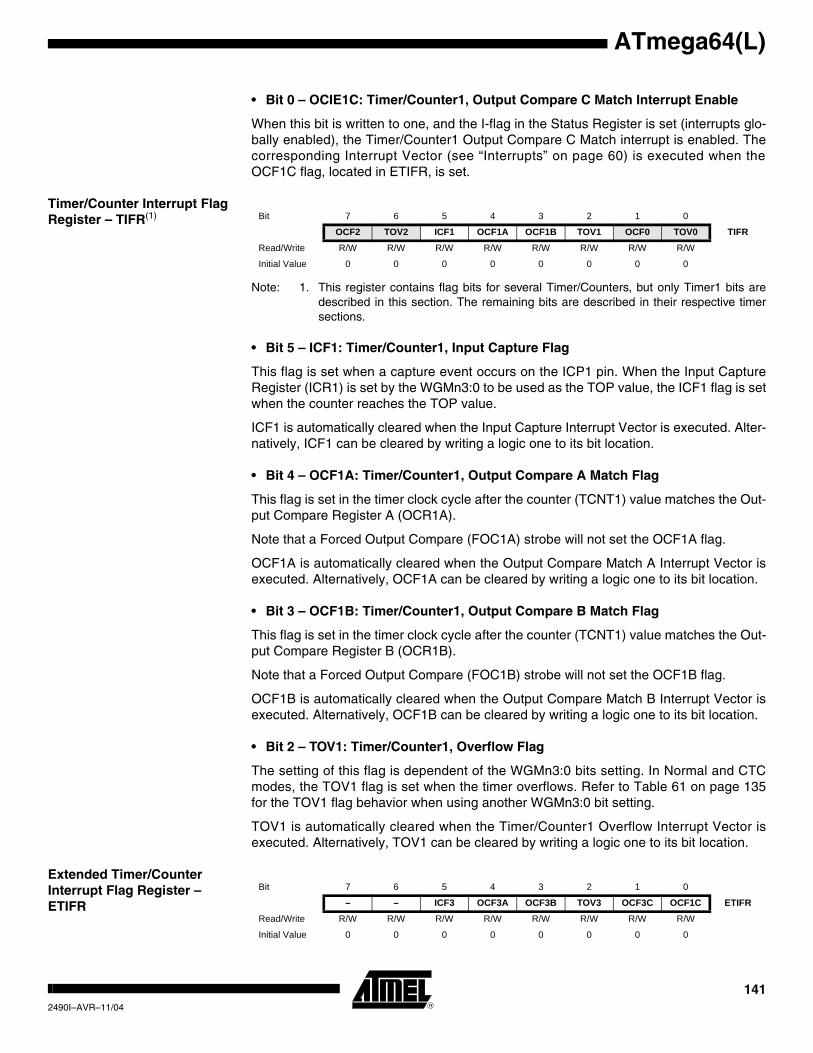
ATmega64(L)
• Bit 0 – OCIE1C: Timer/Counter1, Output Compare C Match Interrupt Enable
When this bit is written to one, and the I-flag in the Status Register is set (interrupts glo-bally enabled), the Timer/Counter1 Output Compare C Match interrupt is enabled. Thecorresponding Interrupt Vector (see “Interrupts” on page 60) is executed when theOCF1C flag, located in ETIFR, is set.
Timer/Counter Interrupt Flag Register – TIFR(1)
Note: 1. This register contains flag bits for several Timer/Counters, but only Timer1 bits aredescribed in this section. The remaining bits are described in their respective timersections.
• Bit 5 – ICF1: Timer/Counter1, Input Capture Flag
This flag is set when a capture event occurs on the ICP1 pin. When the Input CaptureRegister (ICR1) is set by the WGMn3:0 to be used as the TOP value, the ICF1 flag is setwhen the counter reaches the TOP value.
ICF1 is automatically cleared when the Input Capture Interrupt Vector is executed. Alter-natively, ICF1 can be cleared by writing a logic one to its bit location.
• Bit 4 – OCF1A: Timer/Counter1, Output Compare A Match Flag
This flag is set in the timer clock cycle after the counter (TCNT1) value matches the Out-put Compare Register A (OCR1A).
Note that a Forced Output Compare (FOC1A) strobe will not set the OCF1A flag.
OCF1A is automatically cleared when the Output Compare Match A Interrupt Vector isexecuted. Alternatively, OCF1A can be cleared by writing a logic one to its bit location.
• Bit 3 – OCF1B: Timer/Counter1, Output Compare B Match Flag
This flag is set in the timer clock cycle after the counter (TCNT1) value matches the Out-put Compare Register B (OCR1B).
Note that a Forced Output Compare (FOC1B) strobe will not set the OCF1B flag.
OCF1B is automatically cleared when the Output Compare Match B Interrupt Vector isexecuted. Alternatively, OCF1B can be cleared by writing a logic one to its bit location.
• Bit 2 – TOV1: Timer/Counter1, Overflow Flag
The setting of this flag is dependent of the WGMn3:0 bits setting. In Normal and CTCmodes, the TOV1 flag is set when the timer overflows. Refer to Table 61 on page 135for the TOV1 flag behavior when using another WGMn3:0 bit setting.
TOV1 is automatically cleared when the Timer/Counter1 Overflow Interrupt Vector isexecuted. Alternatively, TOV1 can be cleared by writing a logic one to its bit location.
Extended Timer/Counter Interrupt Flag Register – ETIFR
Bit 7 6 5 4 3 2 1 0
OCF2 TOV2 ICF1 OCF1A OCF1B TOV1 OCF0 TOV0 TIFRRead/Write R/W R/W R/W R/W R/W R/W R/W R/W
Initial Value 0 0 0 0 0 0 0 0
Bit 7 6 5 4 3 2 1 0
– – ICF3 OCF3A OCF3B TOV3 OCF3C OCF1C ETIFRRead/Write R/W R/W R/W R/W R/W R/W R/W R/W
Initial Value 0 0 0 0 0 0 0 0
1412490I–AVR–11/04
• Bit 7:6 – Reserved Bits
These bits are reserved for future use. For ensuring compatibility with future devices,these bits must be set to zero when ETIFR is written.
• Bit 5 – ICF3: Timer/Counter3, Input Capture Flag
This flag is set when a capture event occurs on the ICP3 pin. When the Input CaptureRegister (ICR3) is set by the WGM3:0 to be used as the TOP value, the ICF3 flag is setwhen the counter reaches the TOP value.
ICF3 is automatically cleared when the Input Capture 3 Interrupt Vector is executed.Alternatively, ICF3 can be cleared by writing a logic one to its bit location.
• Bit 4 – OCF3A: Timer/Counter3, Output Compare A Match Flag
This flag is set in the timer clock cycle after the counter (TCNT3) value matches the Out-put Compare Register A (OCR3A).
Note that a Forced Output Compare (FOC3A) strobe will not set the OCF3A flag.
OCF3A is automatically cleared when the Output Compare Match 3 A Interrupt Vector isexecuted. Alternatively, OCF3A can be cleared by writing a logic one to its bit location.
• Bit 3 – OCF3B: Timer/Counter3, Output Compare B Match Flag
This flag is set in the timer clock cycle after the counter (TCNT3) value matches the Out-put Compare Register B (OCR3B).
Note that a Forced Output Compare (FOC3B) strobe will not set the OCF3B flag.
OCF3B is automatically cleared when the Output Compare Match 3 B Interrupt Vector isexecuted. Alternatively, OCF3B can be cleared by writing a logic one to its bit location.
• Bit 2 – TOV3: Timer/Counter3, Overflow Flag
The setting of this flag is dependent of the WGM3:0 bits setting. In Normal and CTCmodes, the TOV3 flag is set when the timer overflows. Refer to Table 52 on page 103for the TOV3 flag behavior when using another WGM3:0 bit setting.
TOV3 is automatically cleared when the Timer/Counter3 Overflow Interrupt Vector isexecuted. Alternatively, OCF3B can be cleared by writing a logic one to its bit location.
• Bit 1 – OCF3C: Timer/Counter3, Output Compare C Match Flag
This flag is set in the timer clock cycle after the counter (TCNT3) value matches the Out-put Compare Register C (OCR3C).
Note that a Forced Output Compare (FOC3C) strobe will not set the OCF3C flag.
OCF3C is automatically cleared when the Output Compare Match 3 C Interrupt Vector isexecuted. Alternatively, OCF3C can be cleared by writing a logic one to its bit location.
• Bit 0 – OCF1C: Timer/Counter1, Output Compare C Match Flag
This flag is set in the timer clock cycle after the counter (TCNT1) value matches the Out-put Compare Register C (OCR1C).
Note that a Forced Output Compare (FOC1C) strobe will not set the OCF1C flag.
OCF1C is automatically cleared when the Output Compare Match 1 C Interrupt Vector isexecuted. Alternatively, OCF1C can be cleared by writing a logic one to its bit location.
142 ATmega64(L)2490I–AVR–11/04
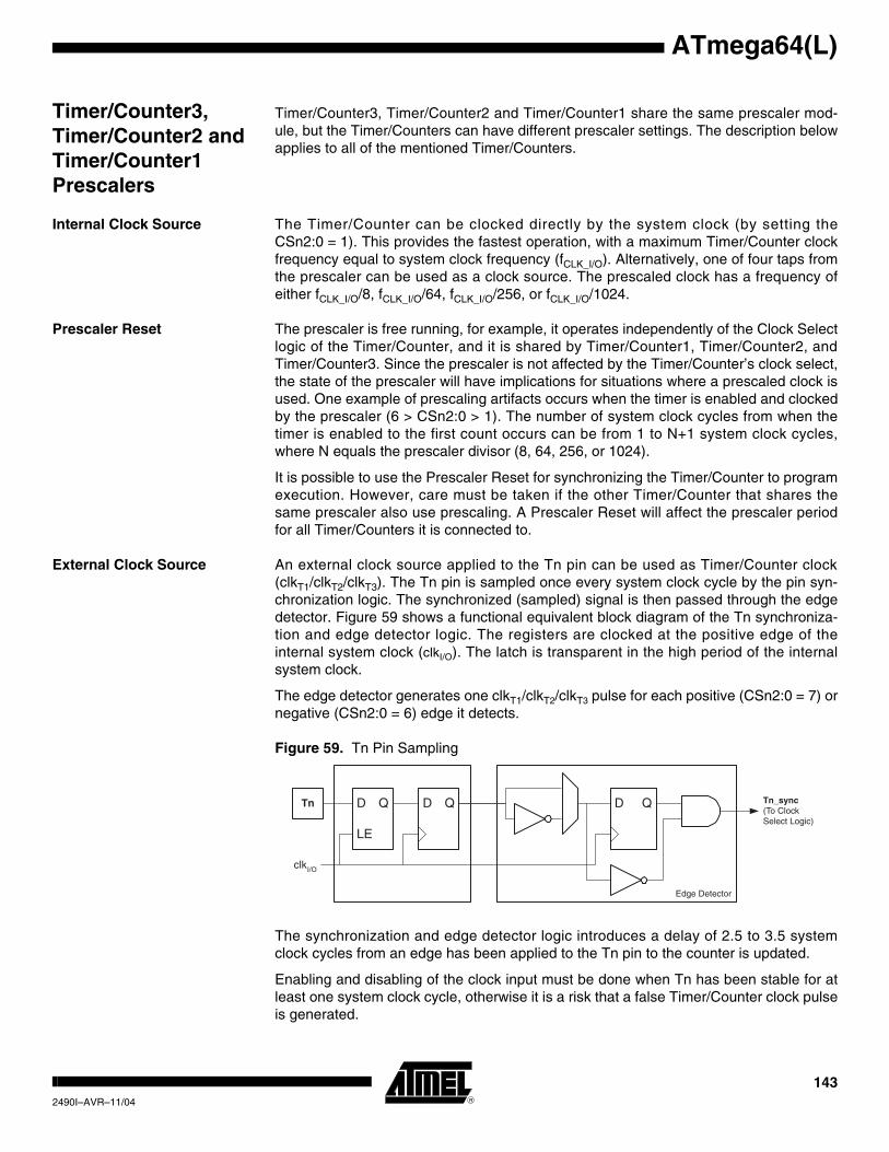
ATmega64(L)
Timer/Counter3, Timer/Counter2 and Timer/Counter1 Prescalers
Timer/Counter3, Timer/Counter2 and Timer/Counter1 share the same prescaler mod-ule, but the Timer/Counters can have different prescaler settings. The description belowapplies to all of the mentioned Timer/Counters.
Internal Clock Source The Timer/Counter can be clocked directly by the system clock (by setting theCSn2:0 = 1). This provides the fastest operation, with a maximum Timer/Counter clockfrequency equal to system clock frequency (fCLK_I/O). Alternatively, one of four taps fromthe prescaler can be used as a clock source. The prescaled clock has a frequency ofeither fCLK_I/O/8, fCLK_I/O/64, fCLK_I/O/256, or fCLK_I/O/1024.
Prescaler Reset The prescaler is free running, for example, it operates independently of the Clock Selectlogic of the Timer/Counter, and it is shared by Timer/Counter1, Timer/Counter2, andTimer/Counter3. Since the prescaler is not affected by the Timer/Counter’s clock select,the state of the prescaler will have implications for situations where a prescaled clock isused. One example of prescaling artifacts occurs when the timer is enabled and clockedby the prescaler (6 > CSn2:0 > 1). The number of system clock cycles from when thetimer is enabled to the first count occurs can be from 1 to N+1 system clock cycles,where N equals the prescaler divisor (8, 64, 256, or 1024).
It is possible to use the Prescaler Reset for synchronizing the Timer/Counter to programexecution. However, care must be taken if the other Timer/Counter that shares thesame prescaler also use prescaling. A Prescaler Reset will affect the prescaler periodfor all Timer/Counters it is connected to.
External Clock Source An external clock source applied to the Tn pin can be used as Timer/Counter clock(clkT1/clkT2/clkT3). The Tn pin is sampled once every system clock cycle by the pin syn-chronization logic. The synchronized (sampled) signal is then passed through the edgedetector. Figure 59 shows a functional equivalent block diagram of the Tn synchroniza-tion and edge detector logic. The registers are clocked at the positive edge of theinternal system clock (clkI/O). The latch is transparent in the high period of the internalsystem clock.
The edge detector generates one clkT1/clkT2/clkT3 pulse for each positive (CSn2:0 = 7) ornegative (CSn2:0 = 6) edge it detects.
Figure 59. Tn Pin Sampling
The synchronization and edge detector logic introduces a delay of 2.5 to 3.5 systemclock cycles from an edge has been applied to the Tn pin to the counter is updated.
Enabling and disabling of the clock input must be done when Tn has been stable for atleast one system clock cycle, otherwise it is a risk that a false Timer/Counter clock pulseis generated.
Tn_sync(To ClockSelect Logic)
Edge Detector
D QD Q
LE
D QTn
clkI/O
1432490I–AVR–11/04
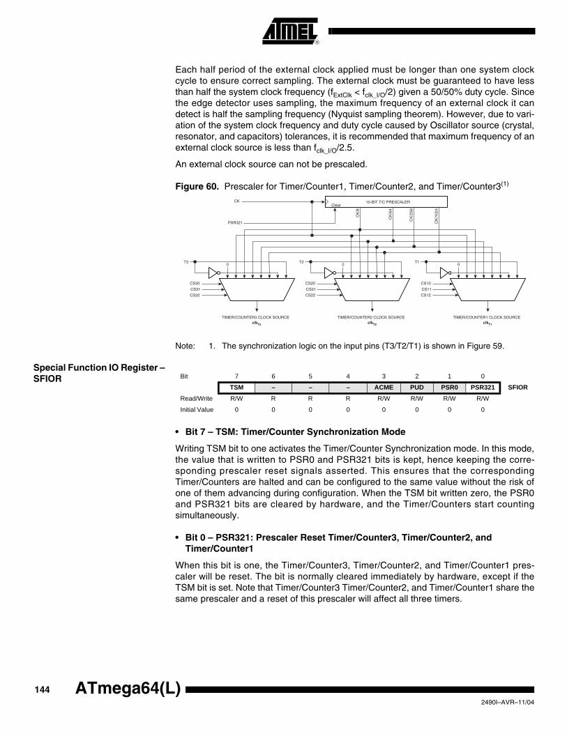
Each half period of the external clock applied must be longer than one system clockcycle to ensure correct sampling. The external clock must be guaranteed to have lessthan half the system clock frequency (fExtClk < fclk_I/O/2) given a 50/50% duty cycle. Sincethe edge detector uses sampling, the maximum frequency of an external clock it candetect is half the sampling frequency (Nyquist sampling theorem). However, due to vari-ation of the system clock frequency and duty cycle caused by Oscillator source (crystal,resonator, and capacitors) tolerances, it is recommended that maximum frequency of anexternal clock source is less than fclk_I/O/2.5.
An external clock source can not be prescaled.
Figure 60. Prescaler for Timer/Counter1, Timer/Counter2, and Timer/Counter3(1)
Note: 1. The synchronization logic on the input pins (T3/T2/T1) is shown in Figure 59.
Special Function IO Register – SFIOR
• Bit 7 – TSM: Timer/Counter Synchronization Mode
Writing TSM bit to one activates the Timer/Counter Synchronization mode. In this mode,the value that is written to PSR0 and PSR321 bits is kept, hence keeping the corre-sponding prescaler reset signals asserted. This ensures that the correspondingTimer/Counters are halted and can be configured to the same value without the risk ofone of them advancing during configuration. When the TSM bit written zero, the PSR0and PSR321 bits are cleared by hardware, and the Timer/Counters start countingsimultaneously.
• Bit 0 – PSR321: Prescaler Reset Timer/Counter3, Timer/Counter2, and Timer/Counter1
When this bit is one, the Timer/Counter3, Timer/Counter2, and Timer/Counter1 pres-caler will be reset. The bit is normally cleared immediately by hardware, except if theTSM bit is set. Note that Timer/Counter3 Timer/Counter2, and Timer/Counter1 share thesame prescaler and a reset of this prescaler will affect all three timers.
PSR321
Clear
clkT2
TIMER/COUNTER2 CLOCK SOURCE
0
CS20
CS21
CS22
T2
clkT1
TIMER/COUNTER1 CLOCK SOURCE
0
CS10
CS11
CS12
T1
clkT3
TIMER/COUNTER3 CLOCK SOURCE
0
CS30
CS31
CS32
T3
10-BIT T/C PRESCALERCK
CK
/8
CK
/64
CK
/256
CK
/102
4
Bit 7 6 5 4 3 2 1 0
TSM – – – ACME PUD PSR0 PSR321 SFIORRead/Write R/W R R R R/W R/W R/W R/W
Initial Value 0 0 0 0 0 0 0 0
144 ATmega64(L)2490I–AVR–11/04
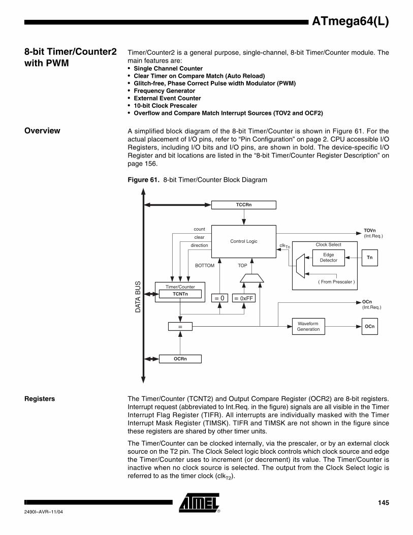
ATmega64(L)
8-bit Timer/Counter2 with PWM
Timer/Counter2 is a general purpose, single-channel, 8-bit Timer/Counter module. Themain features are:• Single Channel Counter• Clear Timer on Compare Match (Auto Reload)• Glitch-free, Phase Correct Pulse width Modulator (PWM)• Frequency Generator• External Event Counter• 10-bit Clock Prescaler• Overflow and Compare Match Interrupt Sources (TOV2 and OCF2)
Overview A simplified block diagram of the 8-bit Timer/Counter is shown in Figure 61. For theactual placement of I/O pins, refer to “Pin Configuration” on page 2. CPU accessible I/ORegisters, including I/O bits and I/O pins, are shown in bold. The device-specific I/ORegister and bit locations are listed in the “8-bit Timer/Counter Register Description” onpage 156.
Figure 61. 8-bit Timer/Counter Block Diagram
Registers The Timer/Counter (TCNT2) and Output Compare Register (OCR2) are 8-bit registers.Interrupt request (abbreviated to Int.Req. in the figure) signals are all visible in the TimerInterrupt Flag Register (TIFR). All interrupts are individually masked with the TimerInterrupt Mask Register (TIMSK). TIFR and TIMSK are not shown in the figure sincethese registers are shared by other timer units.
The Timer/Counter can be clocked internally, via the prescaler, or by an external clocksource on the T2 pin. The Clock Select logic block controls which clock source and edgethe Timer/Counter uses to increment (or decrement) its value. The Timer/Counter isinactive when no clock source is selected. The output from the Clock Select logic isreferred to as the timer clock (clkT2).
Timer/Counter
DAT
A B
US
=
TCNTn
WaveformGeneration
OCn
= 0
Control Logic
= 0xFF
BOTTOM
count
clear
direction
TOVn(Int.Req.)
OCRn
TCCRn
Clock Select
TnEdge
Detector
( From Prescaler )
clkTn
TOP
OCn(Int.Req.)
1452490I–AVR–11/04
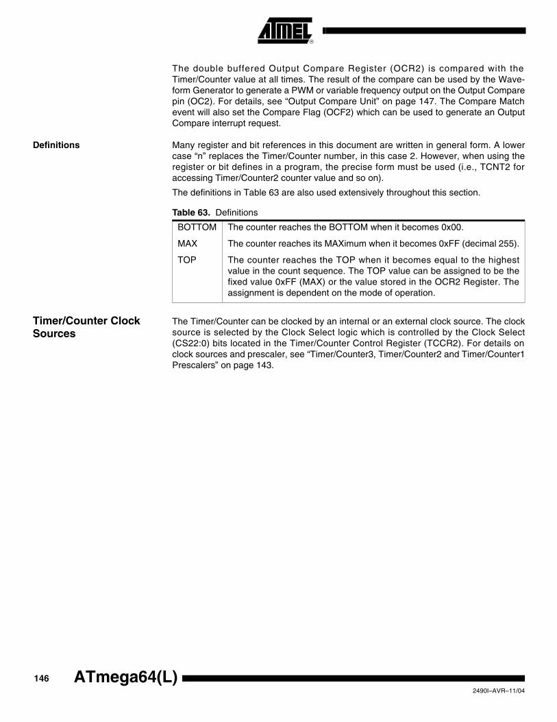
The double buffered Output Compare Register (OCR2) is compared with theTimer/Counter value at all times. The result of the compare can be used by the Wave-form Generator to generate a PWM or variable frequency output on the Output Comparepin (OC2). For details, see “Output Compare Unit” on page 147. The Compare Matchevent will also set the Compare Flag (OCF2) which can be used to generate an OutputCompare interrupt request.
Definitions Many register and bit references in this document are written in general form. A lowercase “n” replaces the Timer/Counter number, in this case 2. However, when using theregister or bit defines in a program, the precise form must be used (i.e., TCNT2 foraccessing Timer/Counter2 counter value and so on).
The definitions in Table 63 are also used extensively throughout this section.
Timer/Counter Clock Sources
The Timer/Counter can be clocked by an internal or an external clock source. The clocksource is selected by the Clock Select logic which is controlled by the Clock Select(CS22:0) bits located in the Timer/Counter Control Register (TCCR2). For details onclock sources and prescaler, see “Timer/Counter3, Timer/Counter2 and Timer/Counter1Prescalers” on page 143.
Table 63. Definitions
BOTTOM The counter reaches the BOTTOM when it becomes 0x00.
MAX The counter reaches its MAXimum when it becomes 0xFF (decimal 255).
TOP The counter reaches the TOP when it becomes equal to the highestvalue in the count sequence. The TOP value can be assigned to be thefixed value 0xFF (MAX) or the value stored in the OCR2 Register. Theassignment is dependent on the mode of operation.
146 ATmega64(L)2490I–AVR–11/04
ATmega64(L)
Counter Unit The main part of the 8-bit Timer/Counter is the programmable bi-directional counter unit.Figure 62 shows a block diagram of the counter and its surroundings.
Figure 62. Counter Unit Block Diagram
Signal description (internal signals):
count Increment or decrement TCNT2 by 1.
direction Select between increment and decrement.
clear Clear TCNT2 (set all bits to zero).
clkTn Timer/counter clock, referred to as clkT0 in the following.
top Signalize that TCNT2 has reached maximum value.
bottom Signalize that TCNT2 has reached minimum value (zero).
Depending of the mode of operation used, the counter is cleared, incremented, or dec-remented at each timer clock (clkT2). clkT2 can be generated from an external or internalclock source, selected by the Clock Select bits (CS22:0). When no clock source isselected (CS22:0 = 0) the timer is stopped. However, the TCNT2 value can be accessedby the CPU, regardless of whether clkT2 is present or not. A CPU write overrides (haspriority over) all counter clear or count operations.
The counting sequence is determined by the setting of the WGM01 and WGM00 bitslocated in the Timer/Counter Control Register (TCCR2). There are close connectionsbetween how the counter behaves (counts) and how waveforms are generated on theOutput Compare output OC2. For more details about advanced counting sequencesand waveform generation, see “Modes of Operation” on page 150.
The Timer/Counter Overflow Flag (TOV2) is set according to the mode of operationselected by the WGM21:0 bits. TOV2 can be used for generating a CPU interrupt.
Output Compare Unit The 8-bit comparator continuously compares TCNT2 with the Output Compare Register(OCR2). Whenever TCNT2 equals OCR2, the comparator signals a match. A match willset the Output Compare Flag (OCF2) at the next timer clock cycle. If enabled (OCIE2 =1 and Global Interrupt Flag in SREG is set), the Output Compare Flag generates anOutput Compare interrupt. The OCF2 flag is automatically cleared when the interrupt isexecuted. Alternatively, the OCF2 flag can be cleared by software by writing a logicalone to its I/O bit location. The Waveform Generator uses the match signal to generatean output according to operating mode set by the WGM21:0 bits and Compare Outputmode (COM21:0) bits. The max and bottom signals are used by the Waveform Genera-tor for handling the special cases of the extreme values in some modes of operation
DATA BUS
TCNTn Control Logic
count
TOVn(Int.Req.)
Clock Select
top
TnEdge
Detector
( From Prescaler )
clkTn
bottom
direction
clear
1472490I–AVR–11/04
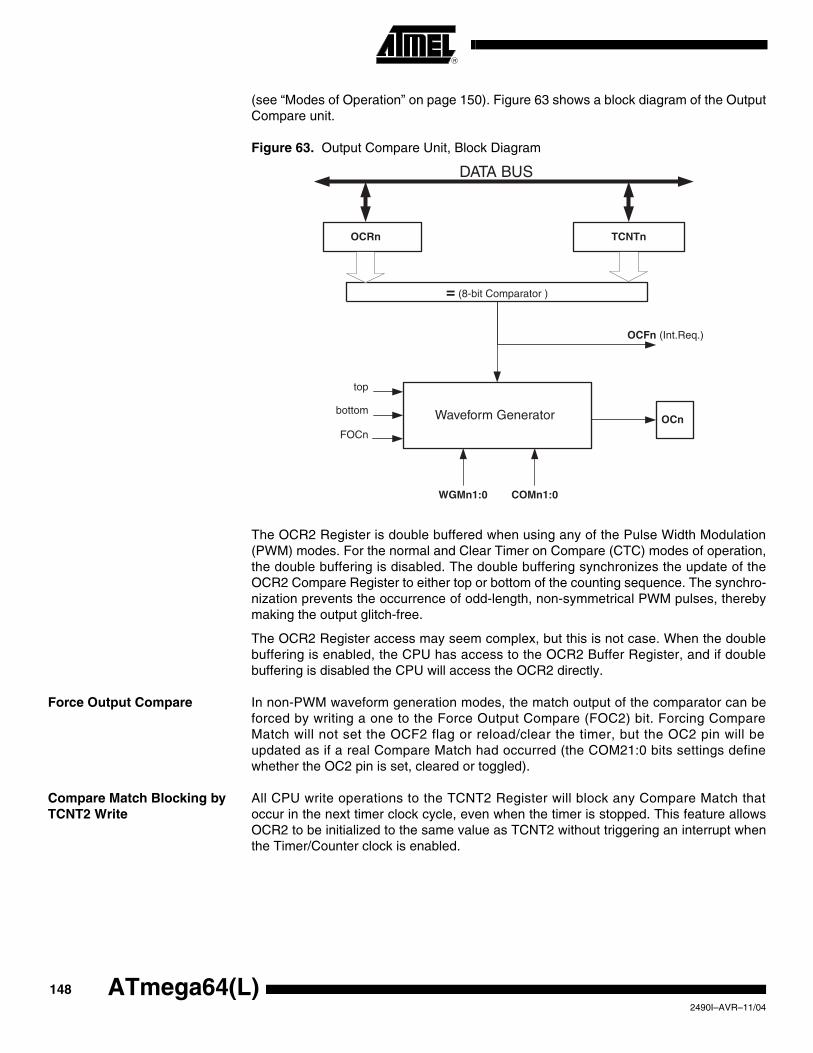
(see “Modes of Operation” on page 150). Figure 63 shows a block diagram of the OutputCompare unit.
Figure 63. Output Compare Unit, Block Diagram
The OCR2 Register is double buffered when using any of the Pulse Width Modulation(PWM) modes. For the normal and Clear Timer on Compare (CTC) modes of operation,the double buffering is disabled. The double buffering synchronizes the update of theOCR2 Compare Register to either top or bottom of the counting sequence. The synchro-nization prevents the occurrence of odd-length, non-symmetrical PWM pulses, therebymaking the output glitch-free.
The OCR2 Register access may seem complex, but this is not case. When the doublebuffering is enabled, the CPU has access to the OCR2 Buffer Register, and if doublebuffering is disabled the CPU will access the OCR2 directly.
Force Output Compare In non-PWM waveform generation modes, the match output of the comparator can beforced by writing a one to the Force Output Compare (FOC2) bit. Forcing CompareMatch will not set the OCF2 flag or reload/clear the timer, but the OC2 pin will beupdated as if a real Compare Match had occurred (the COM21:0 bits settings definewhether the OC2 pin is set, cleared or toggled).
Compare Match Blocking by TCNT2 Write
All CPU write operations to the TCNT2 Register will block any Compare Match thatoccur in the next timer clock cycle, even when the timer is stopped. This feature allowsOCR2 to be initialized to the same value as TCNT2 without triggering an interrupt whenthe Timer/Counter clock is enabled.
OCFn (Int.Req.)
= (8-bit Comparator )
OCRn
OCn
DATA BUS
TCNTn
WGMn1:0
Waveform Generator
top
FOCn
COMn1:0
bottom
148 ATmega64(L)2490I–AVR–11/04
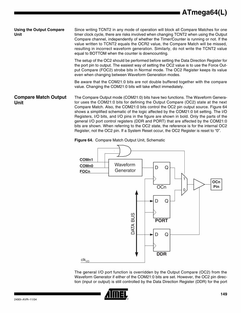
ATmega64(L)
Using the Output Compare Unit
Since writing TCNT2 in any mode of operation will block all Compare Matches for onetimer clock cycle, there are risks involved when changing TCNT2 when using the OutputCompare channel, independently of whether the Timer/Counter is running or not. If thevalue written to TCNT2 equals the OCR2 value, the Compare Match will be missed,resulting in incorrect waveform generation. Similarly, do not write the TCNT2 valueequal to BOTTOM when the counter is downcounting.
The setup of the OC2 should be performed before setting the Data Direction Register forthe port pin to output. The easiest way of setting the OC2 value is to use the Force Out-put Compare (FOC2) strobe bits in Normal mode. The OC2 Register keeps its valueeven when changing between Waveform Generation modes.
Be aware that the COM21:0 bits are not double buffered together with the comparevalue. Changing the COM21:0 bits will take effect immediately.
Compare Match Output Unit
The Compare Output mode (COM21:0) bits have two functions. The Waveform Genera-tor uses the COM21:0 bits for defining the Output Compare (OC2) state at the nextCompare Match. Also, the COM21:0 bits control the OC2 pin output source. Figure 64shows a simplified schematic of the logic affected by the COM21:0 bit setting. The I/ORegisters, I/O bits, and I/O pins in the figure are shown in bold. Only the parts of thegeneral I/O port control registers (DDR and PORT) that are affected by the COM21:0bits are shown. When referring to the OC2 state, the reference is for the internal OC2Register, not the OC2 pin. If a System Reset occur, the OC2 Register is reset to “0”.
Figure 64. Compare Match Output Unit, Schematic
The general I/O port function is overridden by the Output Compare (OC2) from theWaveform Generator if either of the COM21:0 bits are set. However, the OC2 pin direc-tion (input or output) is still controlled by the Data Direction Register (DDR) for the port
PORT
DDR
D Q
D Q
OCnPinOCn
D QWaveformGenerator
COMn1
COMn0
0
1
DAT
A B
US
FOCn
clkI/O
1492490I–AVR–11/04
pin. The Data Direction Register bit for the OC2 pin (DDR_OC2) must be set as outputbefore the OC2 value is visible on the pin. The port override function is independent ofthe Waveform Generation mode.
The design of the Output Compare pin logic allows initialization of the OC2 state beforethe output is enabled. Note that some COM21:0 bit settings are reserved for certainmodes of operation. See “8-bit Timer/Counter Register Description” on page 156.
Compare Output Mode and Waveform Generation
The Waveform Generator uses the COM21:0 bits differently in Normal, CTC, and PWMmodes. For all modes, setting the COM21:0 = 0 tells the Waveform Generator that noaction on the OC2 Register is to be performed on the next Compare Match. For com-pare output actions in the non-PWM modes refer to Table 65 on page 157. For fastPWM mode, refer to Table 66 on page 157, and for phase correct PWM refer to Table67 on page 158.
A change of the COM21:0 bits state will have effect at the first Compare Match after thebits are written. For non-PWM modes, the action can be forced to have immediate effectby using the FOC2 strobe bits.
Modes of Operation The mode of operation, i.e., the behavior of the Timer/Counter and the Output Comparepins, is defined by the combination of the Waveform Generation mode (WGM21:0) andCompare Output mode (COM21:0) bits. The Compare Output mode bits do not affectthe counting sequence, while the Waveform Generation mode bits do. The COM21:0bits control whether the PWM output generated should be inverted or not (inverted ornon-inverted PWM). For non-PWM modes the COM21:0 bits control whether the outputshould be set, cleared, or toggled at a Compare Match (see “Compare Match OutputUnit” on page 149).
For detailed timing information refer to Figure 68, Figure 69, Figure 70, and Figure 71 in“Timer/Counter Timing Diagrams” on page 154.
Normal Mode The simplest mode of operation is the Normal mode (WGM21:0 = 0). In this mode thecounting direction is always up (incrementing), and no counter clear is performed. Thecounter simply overruns when it passes its maximum 8-bit value (TOP = 0xFF) and thenrestarts from the bottom (0x00). In normal operation the Timer/Counter Overflow Flag(TOV2) will be set in the same timer clock cycle as the TCNT2 becomes zero. TheTOV2 flag in this case behaves like a ninth bit, except that it is only set, not cleared.However, combined with the timer overflow interrupt that automatically clears the TOV2flag, the timer resolution can be increased by software. There are no special cases toconsider in the Normal mode, a new counter value can be written anytime.
The Output Compare unit can be used to generate interrupts at some given time. Usingthe Output Compare to generate waveforms in Normal mode is not recommended,since this will occupy too much of the CPU time.
Clear Timer on Compare Match (CTC) Mode
In Clear Timer on Compare or CTC mode (WGM21:0 = 2), the OCR2 Register is used tomanipulate the counter resolution. In CTC mode the counter is cleared to zero when thecounter value (TCNT2) matches the OCR2. The OCR2 defines the top value for thecounter, hence also its resolution. This mode allows greater control of the CompareMatch output frequency. It also simplifies the operation of counting external events.
The timing diagram for the CTC mode is shown in Figure 65. The counter value(TCNT2) increases until a Compare Match occurs between TCNT2 and OCR2, and thencounter (TCNT2) is cleared.
150 ATmega64(L)2490I–AVR–11/04
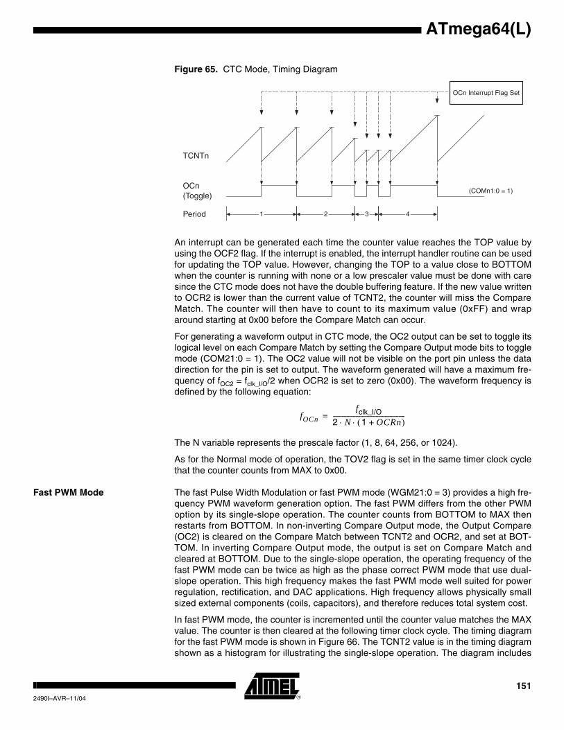
ATmega64(L)
Figure 65. CTC Mode, Timing Diagram
An interrupt can be generated each time the counter value reaches the TOP value byusing the OCF2 flag. If the interrupt is enabled, the interrupt handler routine can be usedfor updating the TOP value. However, changing the TOP to a value close to BOTTOMwhen the counter is running with none or a low prescaler value must be done with caresince the CTC mode does not have the double buffering feature. If the new value writtento OCR2 is lower than the current value of TCNT2, the counter will miss the CompareMatch. The counter will then have to count to its maximum value (0xFF) and wraparound starting at 0x00 before the Compare Match can occur.
For generating a waveform output in CTC mode, the OC2 output can be set to toggle itslogical level on each Compare Match by setting the Compare Output mode bits to togglemode (COM21:0 = 1). The OC2 value will not be visible on the port pin unless the datadirection for the pin is set to output. The waveform generated will have a maximum fre-quency of fOC2 = fclk_I/O/2 when OCR2 is set to zero (0x00). The waveform frequency isdefined by the following equation:
The N variable represents the prescale factor (1, 8, 64, 256, or 1024).
As for the Normal mode of operation, the TOV2 flag is set in the same timer clock cyclethat the counter counts from MAX to 0x00.
Fast PWM Mode The fast Pulse Width Modulation or fast PWM mode (WGM21:0 = 3) provides a high fre-quency PWM waveform generation option. The fast PWM differs from the other PWMoption by its single-slope operation. The counter counts from BOTTOM to MAX thenrestarts from BOTTOM. In non-inverting Compare Output mode, the Output Compare(OC2) is cleared on the Compare Match between TCNT2 and OCR2, and set at BOT-TOM. In inverting Compare Output mode, the output is set on Compare Match andcleared at BOTTOM. Due to the single-slope operation, the operating frequency of thefast PWM mode can be twice as high as the phase correct PWM mode that use dual-slope operation. This high frequency makes the fast PWM mode well suited for powerregulation, rectification, and DAC applications. High frequency allows physically smallsized external components (coils, capacitors), and therefore reduces total system cost.
In fast PWM mode, the counter is incremented until the counter value matches the MAXvalue. The counter is then cleared at the following timer clock cycle. The timing diagramfor the fast PWM mode is shown in Figure 66. The TCNT2 value is in the timing diagramshown as a histogram for illustrating the single-slope operation. The diagram includes
TCNTn
OCn(Toggle)
OCn Interrupt Flag Set
1 4Period 2 3
(COMn1:0 = 1)
fOCnfclk_I/O
2 N 1 OCRn+( )⋅ ⋅-----------------------------------------------=
1512490I–AVR–11/04
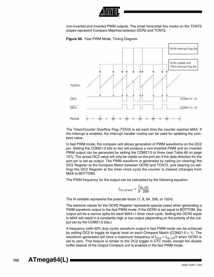
non-inverted and inverted PWM outputs. The small horizontal line marks on the TCNT2slopes represent Compare Matches between OCR2 and TCNT2.
Figure 66. Fast PWM Mode, Timing Diagram
The Timer/Counter Overflow Flag (TOV2) is set each time the counter reaches MAX. Ifthe interrupt is enabled, the interrupt handler routine can be used for updating the com-pare value.
In fast PWM mode, the compare unit allows generation of PWM waveforms on the OC2pin. Setting the COM21:0 bits to two will produce a non-inverted PWM and an invertedPWM output can be generated by setting the COM21:0 to three (see Table 66 on page157). The actual OC2 value will only be visible on the port pin if the data direction for theport pin is set as output. The PWM waveform is generated by setting (or clearing) theOC2 Register at the Compare Match between OCR2 and TCNT2, and clearing (or set-ting) the OC2 Register at the timer clock cycle the counter is cleared (changes fromMAX to BOTTOM).
The PWM frequency for the output can be calculated by the following equation:
The N variable represents the prescale factor (1, 8, 64, 256, or 1024).
The extreme values for the OCR2 Register represents special cases when generating aPWM waveform output in the fast PWM mode. If the OCR2 is set equal to BOTTOM, theoutput will be a narrow spike for each MAX+1 timer clock cycle. Setting the OCR2 equalto MAX will result in a constantly high or low output (depending on the polarity of the out-put set by the COM21:0 bits.)
A frequency (with 50% duty cycle) waveform output in fast PWM mode can be achievedby setting OC2 to toggle its logical level on each Compare Match (COM21:0 = 1). Thewaveform generated will have a maximum frequency of fOC2 = fclk_I/O/2 when OCR2 isset to zero. This feature is similar to the OC2 toggle in CTC mode, except the doublebuffer feature of the Output Compare unit is enabled in the fast PWM mode.
TCNTn
OCRn Update and
TOVn Interrupt Flag Set
1Period 2 3
OCn
OCn
(COMn1:0 = 2)
(COMn1:0 = 3)
OCRn Interrupt Flag Set
4 5 6 7
fOCnPWMfclk_I/O
N 256⋅------------------=
152 ATmega64(L)2490I–AVR–11/04
ATmega64(L)
Phase Correct PWM Mode The phase correct PWM mode (WGM21:0 = 1) provides a high resolution phase correctPWM waveform generation option. The phase correct PWM mode is based on a dual-slope operation. The counter counts repeatedly from BOTTOM to MAX and then fromMAX to BOTTOM. In non-inverting Compare Output mode, the Output Compare (OC2)is cleared on the Compare Match between TCNT2 and OCR2 while upcounting, and seton the Compare Match while downcounting. In inverting Output Compare mode, theoperation is inverted. The dual-slope operation has lower maximum operation frequencythan single slope operation. However, due to the symmetric feature of the dual-slopePWM modes, these modes are preferred for motor control applications.
The PWM resolution for the phase correct PWM mode is fixed to eight bits. In phasecorrect PWM mode the counter is incremented until the counter value matches MAX.When the counter reaches MAX, it changes the count direction. The TCNT2 value willbe equal to MAX for one timer clock cycle. The timing diagram for the phase correctPWM mode is shown on Figure 67. The TCNT2 value is in the timing diagram shown asa histogram for illustrating the dual-slope operation. The diagram includes non-invertedand inverted PWM outputs. The small horizontal line marks on the TCNT2 slopes repre-sent Compare Matches between OCR2 and TCNT2.
Figure 67. Phase Correct PWM Mode, Timing Diagram
The Timer/Counter Overflow Flag (TOV2) is set each time the counter reaches BOT-TOM. The interrupt flag can be used to generate an interrupt each time the counterreaches the BOTTOM value.
In phase correct PWM mode, the compare unit allows generation of PWM waveforms onthe OC2 pin. Setting the COM21:0 bits to two will produce a non-inverted PWM. Aninverted PWM output can be generated by setting the COM21:0 to three (see Table 67on page 158). The actual OC2 value will only be visible on the port pin if the data direc-tion for the port pin is set as output. The PWM waveform is generated by clearing (orsetting) the OC2 Register at the Compare Match between OCR2 and TCNT2 when thecounter increments, and setting (or clearing) the OC2 Register at Compare Match
TOVn Interrupt Flag Set
OCn Interrupt Flag Set
1 2 3
TCNTn
Period
OCn
OCn
(COMn1:0 = 2)
(COMn1:0 = 3)
OCRn Update
1532490I–AVR–11/04
between OCR2 and TCNT2 when the counter decrements. The PWM frequency for theoutput when using phase correct PWM can be calculated by the following equation:
The N variable represents the prescale factor (1, 8, 64, 256, or 1024).
The extreme values for the OCR2 Register represent special cases when generating aPWM waveform output in the phase correct PWM mode. If the OCR2 is set equal toBOTTOM, the output will be continuously low and if set equal to MAX the output will becontinuously high for non-inverted PWM mode. For inverted PWM the output will havethe opposite logic values.
At the very start of period 2 in Figure 67 OCn has a transition from high to low eventhough there is no Compare Match. The point of this transition is to guarantee symmetryaround BOTTOM. There are two cases that give a transition without a Compare Match.
• OCR2 changes its value from MAX, like in Figure 67. When the OCR2 value is MAX the OCn pin value is the same as the result of a down-counting Compare Match. To ensure symmetry around BOTTOM the OCn value at MAX must correspond to the result of an up-counting Compare Match.
• The timer starts counting from a higher value than the one in OCR2, and for that reason misses the Compare Match and hence the OCn change that would have happened on the way up.
Timer/Counter Timing Diagrams
The Timer/Counter is a synchronous design and the timer clock (clkT2) is thereforeshown as a clock enable signal in the following figures. The figures include informationon when interrupt flags are set. Figure 68 contains timing data for basic Timer/Counteroperation. The figure shows the count sequence close to the MAX value in all modesother than phase correct PWM mode.
Figure 68. Timer/Counter Timing Diagram, no Prescaling
Figure 69 shows the same timing data, but with the prescaler enabled.
fOCnPCPWMfclk_I/O
N 510⋅------------------=
clkTn(clkI/O/1)
TOVn
clkI/O
TCNTn MAX - 1 MAX BOTTOM BOTTOM + 1
154 ATmega64(L)2490I–AVR–11/04
ATmega64(L)
Figure 69. Timer/Counter Timing Diagram, with Prescaler (fclk_I/O/8)
Figure 70 shows the setting of OCF2 in all modes except CTC mode.
Figure 70. Timer/Counter Timing Diagram, Setting of OCF2, with Prescaler (fclk_I/O/8)
Figure 71 shows the setting of OCF2 and the clearing of TCNT2 in CTC mode.
TOVn
TCNTn MAX - 1 MAX BOTTOM BOTTOM + 1
clkI/O
clkTn(clkI/O/8)
OCFn
OCRn
TCNTn
OCRn Value
OCRn - 1 OCRn OCRn + 1 OCRn + 2
clkI/O
clkTn(clkI/O/8)
1552490I–AVR–11/04
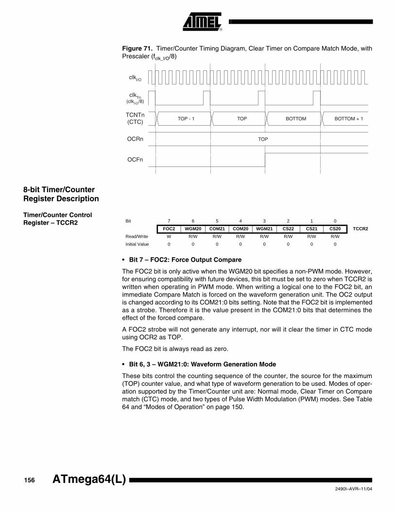
Figure 71. Timer/Counter Timing Diagram, Clear Timer on Compare Match Mode, withPrescaler (fclk_I/O/8)
8-bit Timer/Counter Register Description
Timer/Counter Control Register – TCCR2
• Bit 7 – FOC2: Force Output Compare
The FOC2 bit is only active when the WGM20 bit specifies a non-PWM mode. However,for ensuring compatibility with future devices, this bit must be set to zero when TCCR2 iswritten when operating in PWM mode. When writing a logical one to the FOC2 bit, animmediate Compare Match is forced on the waveform generation unit. The OC2 outputis changed according to its COM21:0 bits setting. Note that the FOC2 bit is implementedas a strobe. Therefore it is the value present in the COM21:0 bits that determines theeffect of the forced compare.
A FOC2 strobe will not generate any interrupt, nor will it clear the timer in CTC modeusing OCR2 as TOP.
The FOC2 bit is always read as zero.
• Bit 6, 3 – WGM21:0: Waveform Generation Mode
These bits control the counting sequence of the counter, the source for the maximum(TOP) counter value, and what type of waveform generation to be used. Modes of oper-ation supported by the Timer/Counter unit are: Normal mode, Clear Timer on Comparematch (CTC) mode, and two types of Pulse Width Modulation (PWM) modes. See Table64 and “Modes of Operation” on page 150.
OCFn
OCRn
TCNTn(CTC)
TOP
TOP - 1 TOP BOTTOM BOTTOM + 1
clkI/O
clkTn(clkI/O/8)
Bit 7 6 5 4 3 2 1 0
FOC2 WGM20 COM21 COM20 WGM21 CS22 CS21 CS20 TCCR2Read/Write W R/W R/W R/W R/W R/W R/W R/W
Initial Value 0 0 0 0 0 0 0 0
156 ATmega64(L)2490I–AVR–11/04
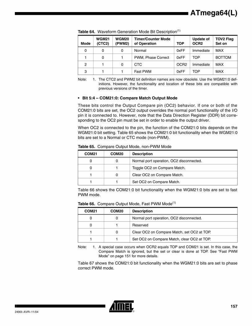
ATmega64(L)
Note: 1. The CTC2 and PWM2 bit definition names are now obsolete. Use the WGM21:0 def-initions. However, the functionality and location of these bits are compatible withprevious versions of the timer.
• Bit 5:4 – COM21:0: Compare Match Output Mode
These bits control the Output Compare pin (OC2) behavior. If one or both of theCOM21:0 bits are set, the OC2 output overrides the normal port functionality of the I/Opin it is connected to. However, note that the Data Direction Register (DDR) bit corre-sponding to the OC2 pin must be set in order to enable the output driver.
When OC2 is connected to the pin, the function of the COM21:0 bits depends on theWGM21:0 bit setting. Table 65 shows the COM21:0 bit functionality when the WGM21:0bits are set to a Normal or CTC mode (non-PWM).
Table 66 shows the COM21:0 bit functionality when the WGM21:0 bits are set to fastPWM mode.
Note: 1. A special case occurs when OCR2 equals TOP and COM21 is set. In this case, theCompare Match is ignored, but the set or clear is done at TOP. See “Fast PWMMode” on page 151 for more details.
Table 67 shows the COM21:0 bit functionality when the WGM21:0 bits are set to phasecorrect PWM mode.
Table 64. Waveform Generation Mode Bit Description(1)
ModeWGM21(CTC2)
WGM20(PWM2)
Timer/Counter Mode of Operation TOP
Update ofOCR2
TOV2 FlagSet on
0 0 0 Normal 0xFF Immediate MAX
1 0 1 PWM, Phase Correct 0xFF TOP BOTTOM
2 1 0 CTC OCR2 Immediate MAX
3 1 1 Fast PWM 0xFF TOP MAX
Table 65. Compare Output Mode, non-PWM Mode
COM21 COM20 Description
0 0 Normal port operation, OC2 disconnected.
0 1 Toggle OC2 on Compare Match.
1 0 Clear OC2 on Compare Match.
1 1 Set OC2 on Compare Match.
Table 66. Compare Output Mode, Fast PWM Mode(1)
COM21 COM20 Description
0 0 Normal port operation, OC2 disconnected.
0 1 Reserved
1 0 Clear OC2 on Compare Match, set OC2 at TOP.
1 1 Set OC2 on Compare Match, clear OC2 at TOP.
1572490I–AVR–11/04
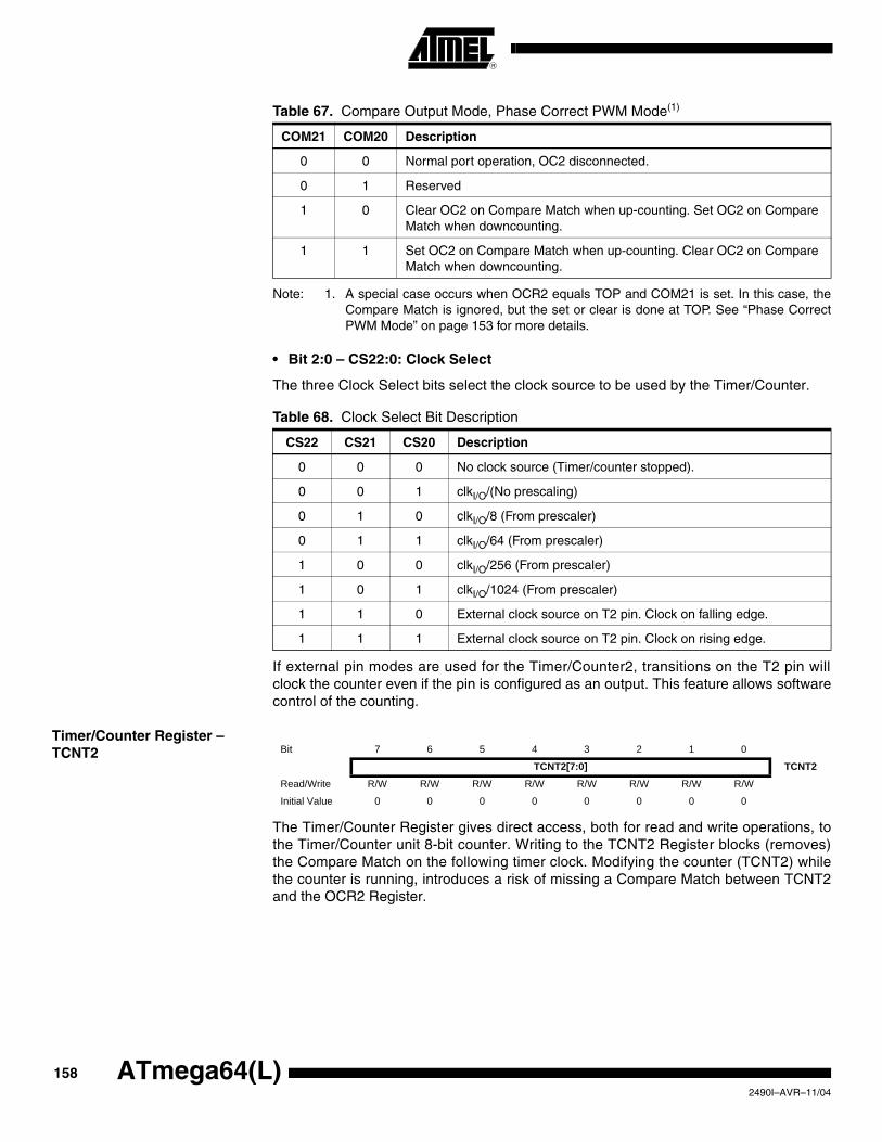
Note: 1. A special case occurs when OCR2 equals TOP and COM21 is set. In this case, theCompare Match is ignored, but the set or clear is done at TOP. See “Phase CorrectPWM Mode” on page 153 for more details.
• Bit 2:0 – CS22:0: Clock Select
The three Clock Select bits select the clock source to be used by the Timer/Counter.
If external pin modes are used for the Timer/Counter2, transitions on the T2 pin willclock the counter even if the pin is configured as an output. This feature allows softwarecontrol of the counting.
Timer/Counter Register – TCNT2
The Timer/Counter Register gives direct access, both for read and write operations, tothe Timer/Counter unit 8-bit counter. Writing to the TCNT2 Register blocks (removes)the Compare Match on the following timer clock. Modifying the counter (TCNT2) whilethe counter is running, introduces a risk of missing a Compare Match between TCNT2and the OCR2 Register.
Table 67. Compare Output Mode, Phase Correct PWM Mode(1)
COM21 COM20 Description
0 0 Normal port operation, OC2 disconnected.
0 1 Reserved
1 0 Clear OC2 on Compare Match when up-counting. Set OC2 on Compare Match when downcounting.
1 1 Set OC2 on Compare Match when up-counting. Clear OC2 on Compare Match when downcounting.
Table 68. Clock Select Bit Description
CS22 CS21 CS20 Description
0 0 0 No clock source (Timer/counter stopped).
0 0 1 clkI/O/(No prescaling)
0 1 0 clkI/O/8 (From prescaler)
0 1 1 clkI/O/64 (From prescaler)
1 0 0 clkI/O/256 (From prescaler)
1 0 1 clkI/O/1024 (From prescaler)
1 1 0 External clock source on T2 pin. Clock on falling edge.
1 1 1 External clock source on T2 pin. Clock on rising edge.
Bit 7 6 5 4 3 2 1 0
TCNT2[7:0] TCNT2Read/Write R/W R/W R/W R/W R/W R/W R/W R/W
Initial Value 0 0 0 0 0 0 0 0
158 ATmega64(L)2490I–AVR–11/04
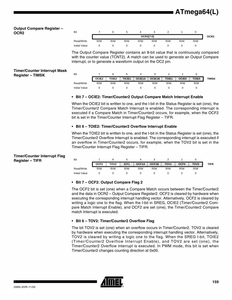
ATmega64(L)
Output Compare Register – OCR2
The Output Compare Register contains an 8-bit value that is continuously comparedwith the counter value (TCNT2). A match can be used to generate an Output Compareinterrupt, or to generate a waveform output on the OC2 pin.
Timer/Counter Interrupt Mask Register – TIMSK
• Bit 7 – OCIE2: Timer/Counter2 Output Compare Match Interrupt Enable
When the OCIE2 bit is written to one, and the I-bit in the Status Register is set (one), theTimer/Counter2 Compare Match Interrupt is enabled. The corresponding interrupt isexecuted if a Compare Match in Timer/Counter2 occurs, for example, when the OCF2bit is set in the Timer/Counter Interrupt Flag Register – TIFR.
• Bit 6 – TOIE2: Timer/Counter2 Overflow Interrupt Enable
When the TOIE2 bit is written to one, and the I-bit in the Status Register is set (one), theTimer/Counter2 Overflow Interrupt is enabled. The corresponding interrupt is executed ifan overflow in Timer/Counter2 occurs, for example, when the TOV2 bit is set in theTimer/Counter Interrupt Flag Register – TIFR.
Timer/Counter Interrupt Flag Register – TIFR
• Bit 7 – OCF2: Output Compare Flag 2
The OCF2 bit is set (one) when a Compare Match occurs between the Timer/Counter2and the data in OCR2 – Output Compare Register2. OCF2 is cleared by hardware whenexecuting the corresponding interrupt handling vector. Alternatively, OCF2 is cleared bywriting a logic one to the flag. When the I-bit in SREG, OCIE2 (Timer/Counter2 Com-pare Match Interrupt Enable), and OCF2 are set (one), the Timer/Counter2 Comparematch Interrupt is executed.
• Bit 6 – TOV2: Timer/Counter2 Overflow Flag
The bit TOV2 is set (one) when an overflow occurs in Timer/Counter2. TOV2 is clearedby hardware when executing the corresponding interrupt handling vector. Alternatively,TOV2 is cleared by writing a logic one to the flag. When the SREG I-bit, TOIE2(Timer/Counter2 Overf low Interrupt Enable), and TOV2 are set (one), theTimer/Counter2 Overflow interrupt is executed. In PWM mode, this bit is set whenTimer/Counter2 changes counting direction at 0x00.
Bit 7 6 5 4 3 2 1 0
OCR2[7:0] OCR2Read/Write R/W R/W R/W R/W R/W R/W R/W R/W
Initial Value 0 0 0 0 0 0 0 0
Bit 7 6 5 4 3 2 1 0
OCIE2 TOIE2 TICIE1 OCIE1A OCIE1B TOIE1 OCIE0 TOIE0 TIMSKRead/Write R/W R/W R/W R/W R/W R/W R/W R/W
Initial Value 0 0 0 0 0 0 0 0
Bit 7 6 5 4 3 2 1 0
OCF2 TOV2 ICF1 OCF1A OCF1B TOV1 OCF0 TOV0 TIFRRead/Write R/W R/W R/W R/W R/W R/W R/W R/W
Initial Value 0 0 0 0 0 0 0 0
1592490I–AVR–11/04
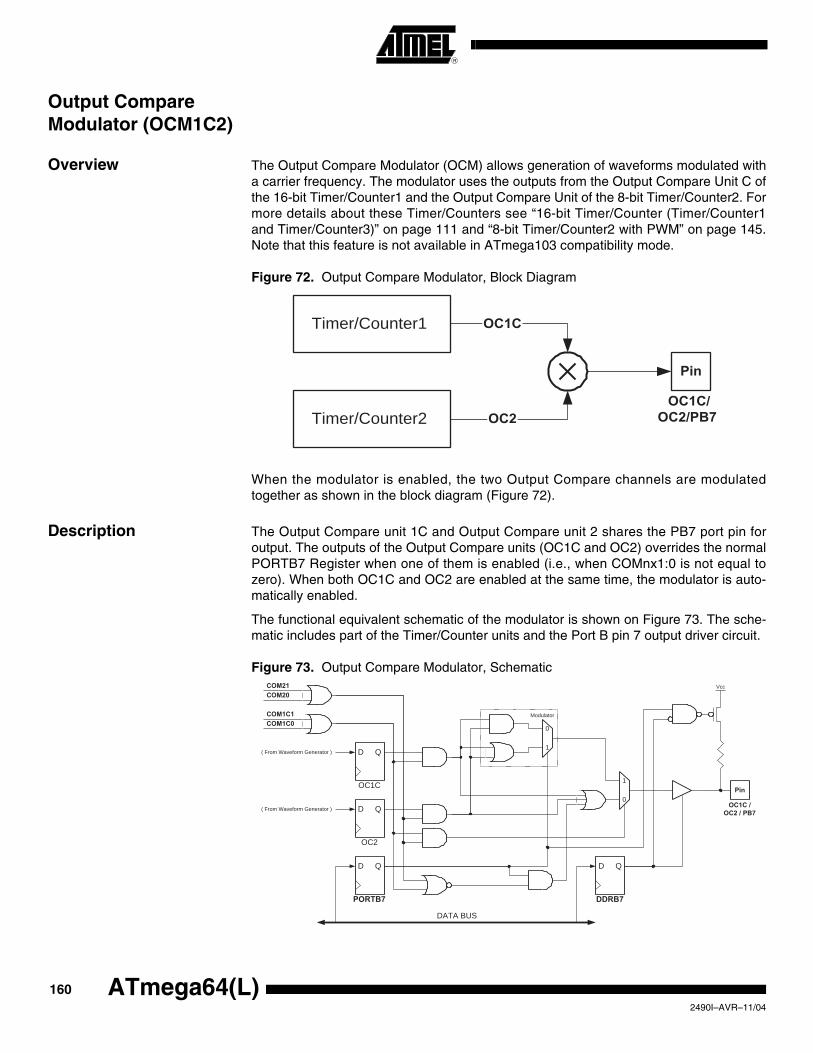
Output Compare Modulator (OCM1C2)
Overview The Output Compare Modulator (OCM) allows generation of waveforms modulated witha carrier frequency. The modulator uses the outputs from the Output Compare Unit C ofthe 16-bit Timer/Counter1 and the Output Compare Unit of the 8-bit Timer/Counter2. Formore details about these Timer/Counters see “16-bit Timer/Counter (Timer/Counter1and Timer/Counter3)” on page 111 and “8-bit Timer/Counter2 with PWM” on page 145.Note that this feature is not available in ATmega103 compatibility mode.
Figure 72. Output Compare Modulator, Block Diagram
When the modulator is enabled, the two Output Compare channels are modulatedtogether as shown in the block diagram (Figure 72).
Description The Output Compare unit 1C and Output Compare unit 2 shares the PB7 port pin foroutput. The outputs of the Output Compare units (OC1C and OC2) overrides the normalPORTB7 Register when one of them is enabled (i.e., when COMnx1:0 is not equal tozero). When both OC1C and OC2 are enabled at the same time, the modulator is auto-matically enabled.
The functional equivalent schematic of the modulator is shown on Figure 73. The sche-matic includes part of the Timer/Counter units and the Port B pin 7 output driver circuit.
Figure 73. Output Compare Modulator, Schematic
OC1C
Pin
OC1C/OC2/PB7
Timer/Counter1
Timer/Counter2 OC2
PORTB7 DDRB7
D QD Q
Pin
COM21COM20
DATA BUS
OC1C /OC2 / PB7
COM1C1COM1C0
Modulator
1
0
OC1C
D Q
OC2
D Q
( From Waveform Generator )
( From Waveform Generator )
0
1
Vcc
160 ATmega64(L)2490I–AVR–11/04
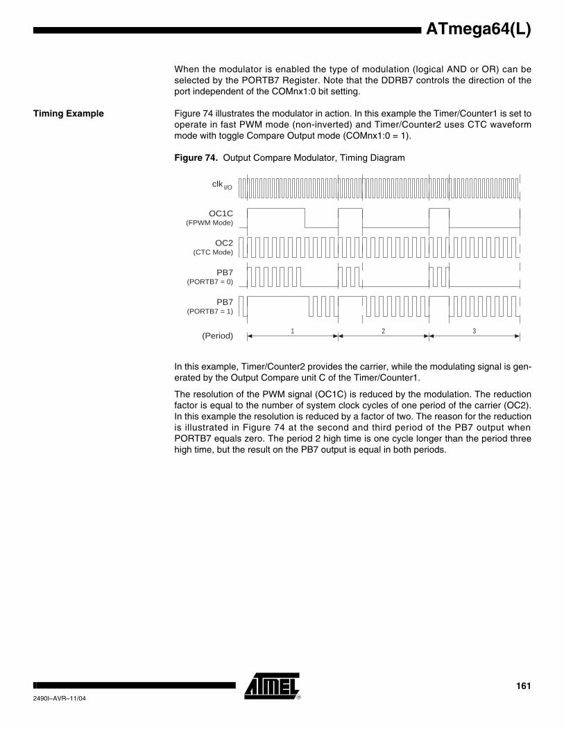
ATmega64(L)
When the modulator is enabled the type of modulation (logical AND or OR) can beselected by the PORTB7 Register. Note that the DDRB7 controls the direction of theport independent of the COMnx1:0 bit setting.
Timing Example Figure 74 illustrates the modulator in action. In this example the Timer/Counter1 is set tooperate in fast PWM mode (non-inverted) and Timer/Counter2 uses CTC waveformmode with toggle Compare Output mode (COMnx1:0 = 1).
Figure 74. Output Compare Modulator, Timing Diagram
In this example, Timer/Counter2 provides the carrier, while the modulating signal is gen-erated by the Output Compare unit C of the Timer/Counter1.
The resolution of the PWM signal (OC1C) is reduced by the modulation. The reductionfactor is equal to the number of system clock cycles of one period of the carrier (OC2).In this example the resolution is reduced by a factor of two. The reason for the reductionis illustrated in Figure 74 at the second and third period of the PB7 output whenPORTB7 equals zero. The period 2 high time is one cycle longer than the period threehigh time, but the result on the PB7 output is equal in both periods.
1 2
OC2(CTC Mode)
OC1C(FPWM Mode)
PB7(PORTB7 = 0)
PB7(PORTB7 = 1)
(Period) 3
clk I/O
1612490I–AVR–11/04
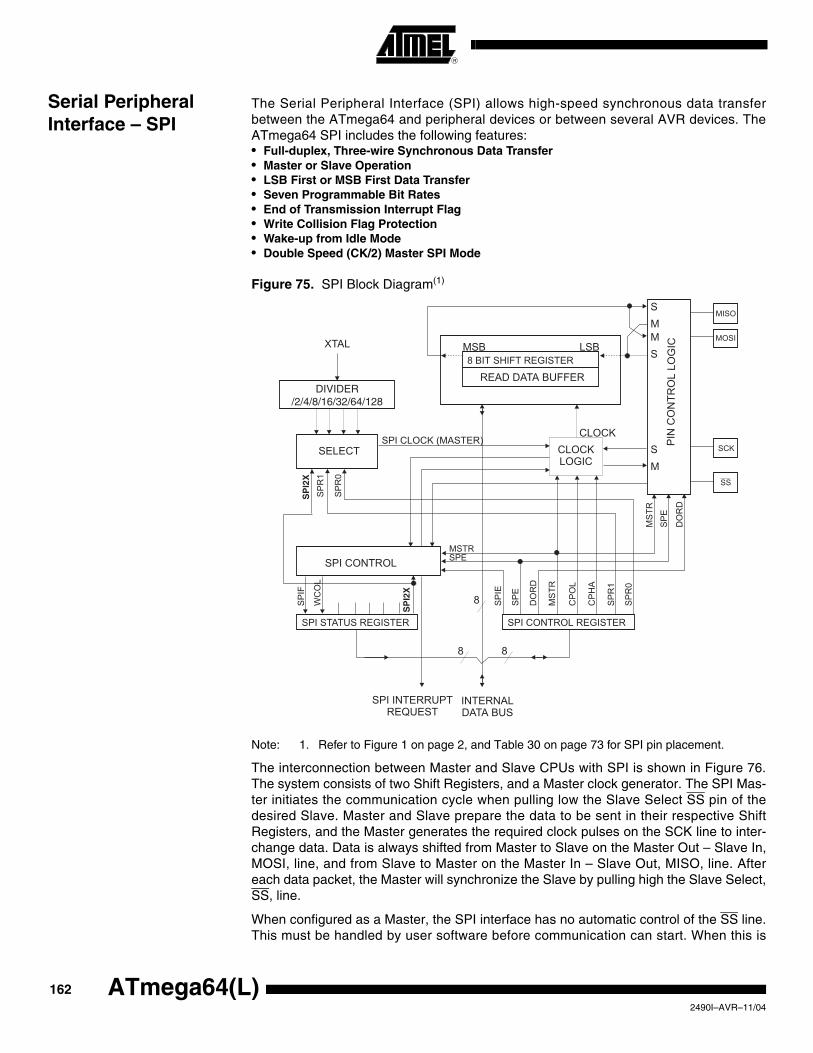
Serial Peripheral Interface – SPI
The Serial Peripheral Interface (SPI) allows high-speed synchronous data transferbetween the ATmega64 and peripheral devices or between several AVR devices. TheATmega64 SPI includes the following features:• Full-duplex, Three-wire Synchronous Data Transfer• Master or Slave Operation• LSB First or MSB First Data Transfer• Seven Programmable Bit Rates• End of Transmission Interrupt Flag• Write Collision Flag Protection• Wake-up from Idle Mode• Double Speed (CK/2) Master SPI Mode
Figure 75. SPI Block Diagram(1)
Note: 1. Refer to Figure 1 on page 2, and Table 30 on page 73 for SPI pin placement.
The interconnection between Master and Slave CPUs with SPI is shown in Figure 76.The system consists of two Shift Registers, and a Master clock generator. The SPI Mas-ter initiates the communication cycle when pulling low the Slave Select SS pin of thedesired Slave. Master and Slave prepare the data to be sent in their respective ShiftRegisters, and the Master generates the required clock pulses on the SCK line to inter-change data. Data is always shifted from Master to Slave on the Master Out – Slave In,MOSI, line, and from Slave to Master on the Master In – Slave Out, MISO, line. Aftereach data packet, the Master will synchronize the Slave by pulling high the Slave Select,SS, line.
When configured as a Master, the SPI interface has no automatic control of the SS line.This must be handled by user software before communication can start. When this is
SP
I2X
SP
I2X
DIVIDER/2/4/8/16/32/64/128
162 ATmega64(L)2490I–AVR–11/04
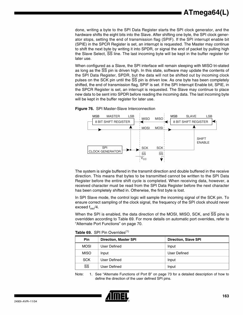
ATmega64(L)
done, writing a byte to the SPI Data Register starts the SPI clock generator, and thehardware shifts the eight bits into the Slave. After shifting one byte, the SPI clock gener-ator stops, setting the end of transmission flag (SPIF). If the SPI interrupt enable bit(SPIE) in the SPCR Register is set, an interrupt is requested. The Master may continueto shift the next byte by writing it into SPDR, or signal the end of packet by pulling highthe Slave Select, SS line. The last incoming byte will be kept in the buffer register forlater use.
When configured as a Slave, the SPI interface will remain sleeping with MISO tri-statedas long as the SS pin is driven high. In this state, software may update the contents ofthe SPI Data Register, SPDR, but the data will not be shifted out by incoming clockpulses on the SCK pin until the SS pin is driven low. As one byte has been completelyshifted, the end of transmission flag, SPIF is set. If the SPI Interrupt Enable bit, SPIE, inthe SPCR Register is set, an interrupt is requested. The Slave may continue to placenew data to be sent into SPDR before reading the incoming data. The last incoming bytewill be kept in the buffer register for later use.
Figure 76. SPI Master-Slave Interconnection
The system is single buffered in the transmit direction and double buffered in the receivedirection. This means that bytes to be transmitted cannot be written to the SPI DataRegister before the entire shift cycle is completed. When receiving data, however, areceived character must be read from the SPI Data Register before the next characterhas been completely shifted in. Otherwise, the first byte is lost.
In SPI Slave mode, the control logic will sample the incoming signal of the SCK pin. Toensure correct sampling of the clock signal, the frequency of the SPI clock should neverexceed fosc/4.
When the SPI is enabled, the data direction of the MOSI, MISO, SCK, and SS pins isoverridden according to Table 69. For more details on automatic port overrides, refer to“Alternate Port Functions” on page 70.
Note: 1. See “Alternate Functions of Port B” on page 73 for a detailed description of how todefine the direction of the user defined SPI pins.
Table 69. SPI Pin Overrides(1)
Pin Direction, Master SPI Direction, Slave SPI
MOSI User Defined Input
MISO Input User Defined
SCK User Defined Input
SS User Defined Input
MSB MASTER LSB
8 BIT SHIFT REGISTER
MSB SLAVE LSB
8 BIT SHIFT REGISTERMISO
MOSI
SPICLOCK GENERATOR
SCK
SS
MISO
MOSI
SCK
SSVCC
SHIFTENABLE
1632490I–AVR–11/04
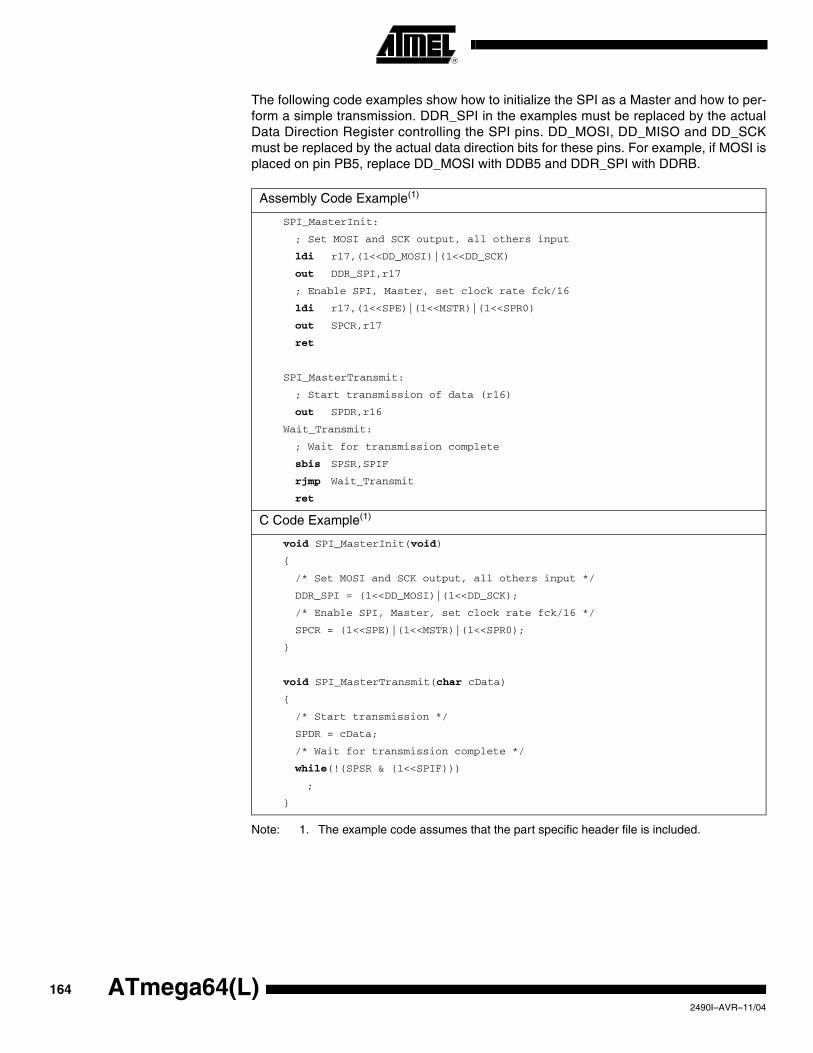
The following code examples show how to initialize the SPI as a Master and how to per-form a simple transmission. DDR_SPI in the examples must be replaced by the actualData Direction Register controlling the SPI pins. DD_MOSI, DD_MISO and DD_SCKmust be replaced by the actual data direction bits for these pins. For example, if MOSI isplaced on pin PB5, replace DD_MOSI with DDB5 and DDR_SPI with DDRB.
Note: 1. The example code assumes that the part specific header file is included.
Assembly Code Example(1)
SPI_MasterInit:
; Set MOSI and SCK output, all others input
ldi r17,(1<<DD_MOSI)|(1<<DD_SCK)
out DDR_SPI,r17
; Enable SPI, Master, set clock rate fck/16
ldi r17,(1<<SPE)|(1<<MSTR)|(1<<SPR0)
out SPCR,r17
ret
SPI_MasterTransmit:
; Start transmission of data (r16)
out SPDR,r16
Wait_Transmit:
; Wait for transmission complete
sbis SPSR,SPIF
rjmp Wait_Transmit
ret
C Code Example(1)
void SPI_MasterInit(void)
/* Set MOSI and SCK output, all others input */
DDR_SPI = (1<<DD_MOSI)|(1<<DD_SCK);
/* Enable SPI, Master, set clock rate fck/16 */
SPCR = (1<<SPE)|(1<<MSTR)|(1<<SPR0);
void SPI_MasterTransmit(char cData)
/* Start transmission */
SPDR = cData;
/* Wait for transmission complete */
while(!(SPSR & (1<<SPIF)))
;
164 ATmega64(L)2490I–AVR–11/04
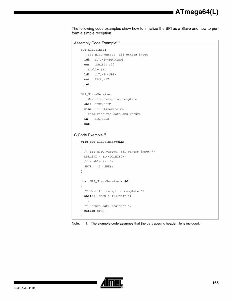
ATmega64(L)
The following code examples show how to initialize the SPI as a Slave and how to per-form a simple reception.
Note: 1. The example code assumes that the part specific header file is included.
Assembly Code Example(1)
SPI_SlaveInit:
; Set MISO output, all others input
ldi r17,(1<<DD_MISO)
out DDR_SPI,r17
; Enable SPI
ldi r17,(1<<SPE)
out SPCR,r17
ret
SPI_SlaveReceive:
; Wait for reception complete
sbis SPSR,SPIF
rjmp SPI_SlaveReceive
; Read received data and return
in r16,SPDR
ret
C Code Example(1)
void SPI_SlaveInit(void)
/* Set MISO output, all others input */
DDR_SPI = (1<<DD_MISO);
/* Enable SPI */
SPCR = (1<<SPE);
char SPI_SlaveReceive(void)
/* Wait for reception complete */
while(!(SPSR & (1<<SPIF)))
;
/* Return data register */
return SPDR;
1652490I–AVR–11/04
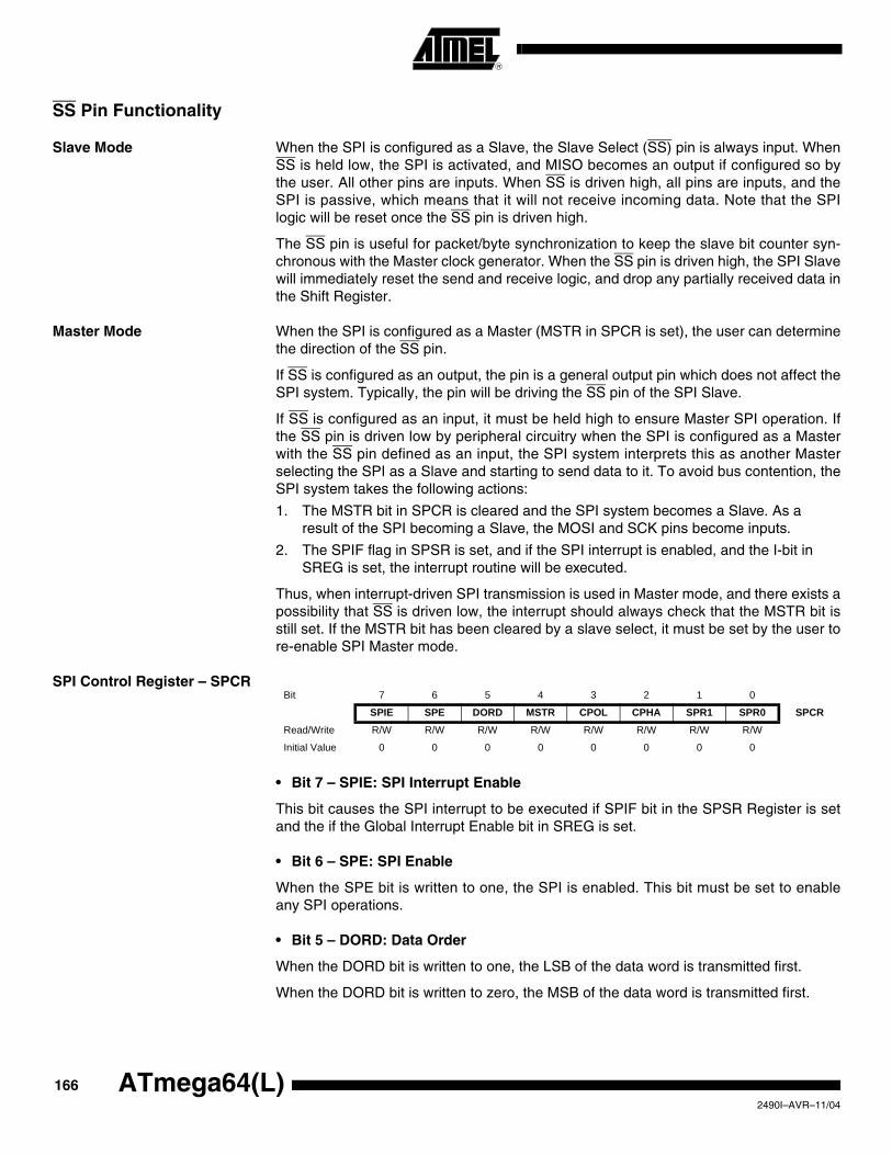
SS Pin Functionality
Slave Mode When the SPI is configured as a Slave, the Slave Select (SS) pin is always input. WhenSS is held low, the SPI is activated, and MISO becomes an output if configured so bythe user. All other pins are inputs. When SS is driven high, all pins are inputs, and theSPI is passive, which means that it will not receive incoming data. Note that the SPIlogic will be reset once the SS pin is driven high.
The SS pin is useful for packet/byte synchronization to keep the slave bit counter syn-chronous with the Master clock generator. When the SS pin is driven high, the SPI Slavewill immediately reset the send and receive logic, and drop any partially received data inthe Shift Register.
Master Mode When the SPI is configured as a Master (MSTR in SPCR is set), the user can determinethe direction of the SS pin.
If SS is configured as an output, the pin is a general output pin which does not affect theSPI system. Typically, the pin will be driving the SS pin of the SPI Slave.
If SS is configured as an input, it must be held high to ensure Master SPI operation. Ifthe SS pin is driven low by peripheral circuitry when the SPI is configured as a Masterwith the SS pin defined as an input, the SPI system interprets this as another Masterselecting the SPI as a Slave and starting to send data to it. To avoid bus contention, theSPI system takes the following actions:
1. The MSTR bit in SPCR is cleared and the SPI system becomes a Slave. As a result of the SPI becoming a Slave, the MOSI and SCK pins become inputs.
2. The SPIF flag in SPSR is set, and if the SPI interrupt is enabled, and the I-bit in SREG is set, the interrupt routine will be executed.
Thus, when interrupt-driven SPI transmission is used in Master mode, and there exists apossibility that SS is driven low, the interrupt should always check that the MSTR bit isstill set. If the MSTR bit has been cleared by a slave select, it must be set by the user tore-enable SPI Master mode.
SPI Control Register – SPCR
• Bit 7 – SPIE: SPI Interrupt Enable
This bit causes the SPI interrupt to be executed if SPIF bit in the SPSR Register is setand the if the Global Interrupt Enable bit in SREG is set.
• Bit 6 – SPE: SPI Enable
When the SPE bit is written to one, the SPI is enabled. This bit must be set to enableany SPI operations.
• Bit 5 – DORD: Data Order
When the DORD bit is written to one, the LSB of the data word is transmitted first.
When the DORD bit is written to zero, the MSB of the data word is transmitted first.
Bit 7 6 5 4 3 2 1 0
SPIE SPE DORD MSTR CPOL CPHA SPR1 SPR0 SPCRRead/Write R/W R/W R/W R/W R/W R/W R/W R/W
Initial Value 0 0 0 0 0 0 0 0
166 ATmega64(L)2490I–AVR–11/04
ATmega64(L)
• Bit 4 – MSTR: Master/Slave Select
This bit selects Master SPI mode when written to one, and Slave SPI mode when writtenlogic zero. If SS is configured as an input and is driven low while MSTR is set, MSTR willbe cleared, and SPIF in SPSR will become set. The user will then have to set MSTR tore-enable SPI Master mode.
• Bit 3 – CPOL: Clock Polarity
When this bit is written to one, SCK is high when idle. When CPOL is written to zero,SCK is low when idle. Refer to Figure 77 and Figure 78 for an example. The CPOL func-tionality is summarized below:
• Bit 2 – CPHA: Clock Phase
The settings of the Clock Phase bit (CPHA) determine if data is sampled on the leading(first) or trailing (last) edge of SCK. Refer to Figure 77 and Figure 78 for an example.The CPHA functionality is summarized below:
• Bits 1, 0 – SPR1, SPR0: SPI Clock Rate Select 1 and 0
These two bits control the SCK rate of the device configured as a master. SPR1 andSPR0 have no effect on the slave. The relationship between SCK and the OscillatorClock frequency fosc is shown in Table 72.
Table 70. CPOL Functionality
CPOL Leading Edge Trailing Edge
0 Rising Falling
1 Falling Rising
Table 71. CPHA Functionality
CPHA Leading Edge Trailing Edge
0 Sample Setup
1 Setup Sample
Table 72. Relationship Between SCK and the Oscillator Frequency
SPI2X SPR1 SPR0 SCK Frequency
0 0 0 fosc/4
0 0 1 fosc/16
0 1 0 fosc/64
0 1 1 fosc/128
1 0 0 fosc/2
1 0 1 fosc/8
1 1 0 fosc/32
1 1 1 fosc/64
1672490I–AVR–11/04
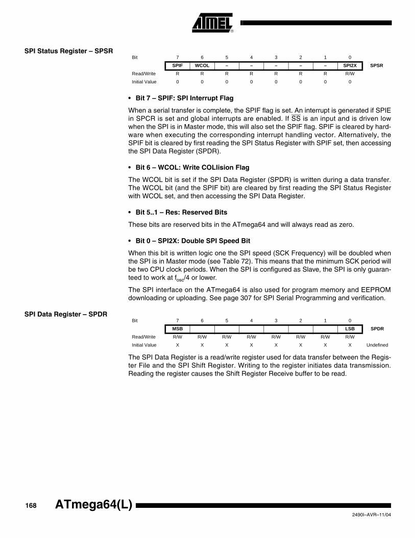
SPI Status Register – SPSR
• Bit 7 – SPIF: SPI Interrupt Flag
When a serial transfer is complete, the SPIF flag is set. An interrupt is generated if SPIEin SPCR is set and global interrupts are enabled. If SS is an input and is driven lowwhen the SPI is in Master mode, this will also set the SPIF flag. SPIF is cleared by hard-ware when executing the corresponding interrupt handling vector. Alternatively, theSPIF bit is cleared by first reading the SPI Status Register with SPIF set, then accessingthe SPI Data Register (SPDR).
• Bit 6 – WCOL: Write COLlision Flag
The WCOL bit is set if the SPI Data Register (SPDR) is written during a data transfer.The WCOL bit (and the SPIF bit) are cleared by first reading the SPI Status Registerwith WCOL set, and then accessing the SPI Data Register.
• Bit 5..1 – Res: Reserved Bits
These bits are reserved bits in the ATmega64 and will always read as zero.
• Bit 0 – SPI2X: Double SPI Speed Bit
When this bit is written logic one the SPI speed (SCK Frequency) will be doubled whenthe SPI is in Master mode (see Table 72). This means that the minimum SCK period willbe two CPU clock periods. When the SPI is configured as Slave, the SPI is only guaran-teed to work at fosc/4 or lower.
The SPI interface on the ATmega64 is also used for program memory and EEPROMdownloading or uploading. See page 307 for SPI Serial Programming and verification.
SPI Data Register – SPDR
The SPI Data Register is a read/write register used for data transfer between the Regis-ter File and the SPI Shift Register. Writing to the register initiates data transmission.Reading the register causes the Shift Register Receive buffer to be read.
Bit 7 6 5 4 3 2 1 0
SPIF WCOL – – – – – SPI2X SPSRRead/Write R R R R R R R R/W
Initial Value 0 0 0 0 0 0 0 0
Bit 7 6 5 4 3 2 1 0
MSB LSB SPDRRead/Write R/W R/W R/W R/W R/W R/W R/W R/W
Initial Value X X X X X X X X Undefined
168 ATmega64(L)2490I–AVR–11/04
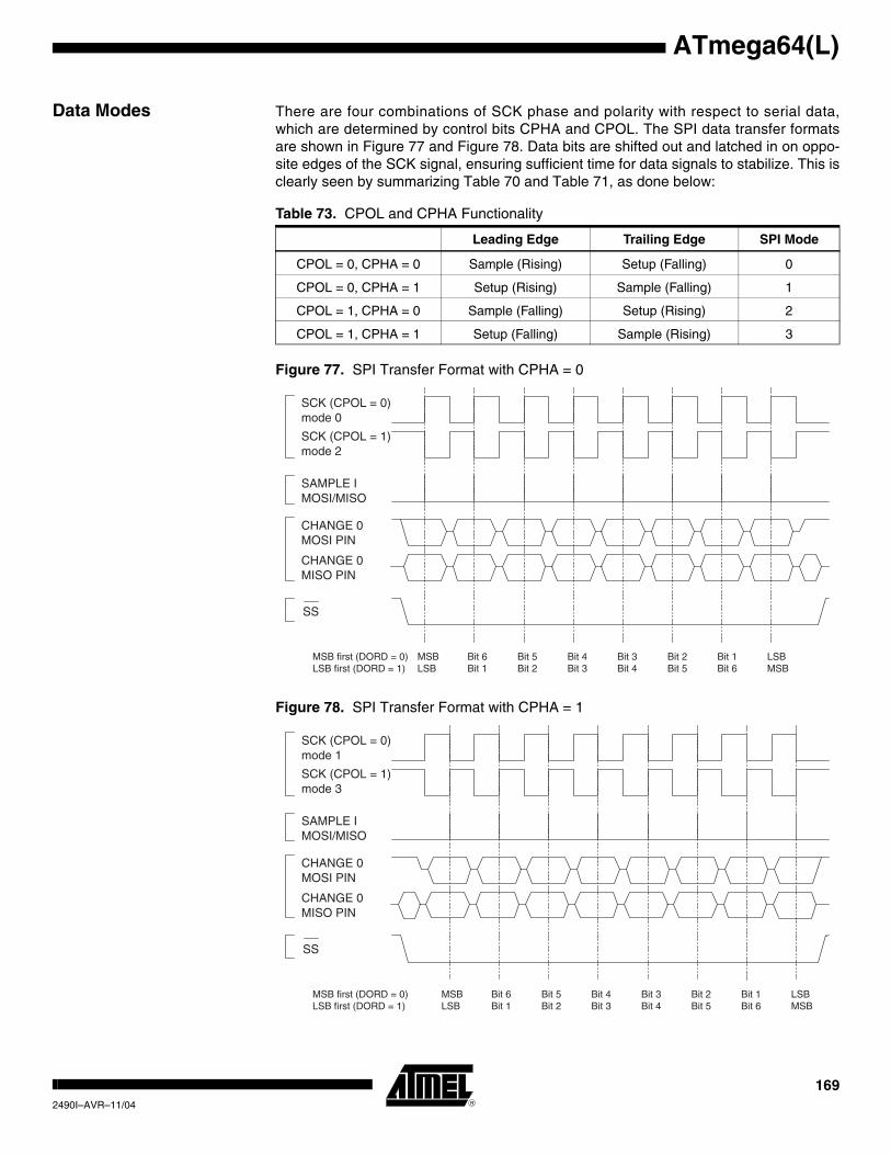
ATmega64(L)
Data Modes There are four combinations of SCK phase and polarity with respect to serial data,which are determined by control bits CPHA and CPOL. The SPI data transfer formatsare shown in Figure 77 and Figure 78. Data bits are shifted out and latched in on oppo-site edges of the SCK signal, ensuring sufficient time for data signals to stabilize. This isclearly seen by summarizing Table 70 and Table 71, as done below:
Figure 77. SPI Transfer Format with CPHA = 0
Figure 78. SPI Transfer Format with CPHA = 1
Table 73. CPOL and CPHA Functionality
Leading Edge Trailing Edge SPI Mode
CPOL = 0, CPHA = 0 Sample (Rising) Setup (Falling) 0
CPOL = 0, CPHA = 1 Setup (Rising) Sample (Falling) 1
CPOL = 1, CPHA = 0 Sample (Falling) Setup (Rising) 2
CPOL = 1, CPHA = 1 Setup (Falling) Sample (Rising) 3
Bit 1Bit 6
LSBMSB
SCK (CPOL = 0)mode 0
SAMPLE IMOSI/MISO
CHANGE 0MOSI PIN
CHANGE 0MISO PIN
SCK (CPOL = 1)mode 2
SS
MSBLSB
Bit 6Bit 1
Bit 5Bit 2
Bit 4Bit 3
Bit 3Bit 4
Bit 2Bit 5
MSB first (DORD = 0)LSB first (DORD = 1)
SCK (CPOL = 0)mode 1
SAMPLE IMOSI/MISO
CHANGE 0MOSI PIN
CHANGE 0MISO PIN
SCK (CPOL = 1)mode 3
SS
MSBLSB
Bit 6Bit 1
Bit 5Bit 2
Bit 4Bit 3
Bit 3Bit 4
Bit 2Bit 5
Bit 1Bit 6
LSBMSB
MSB first (DORD = 0)LSB first (DORD = 1)
1692490I–AVR–11/04
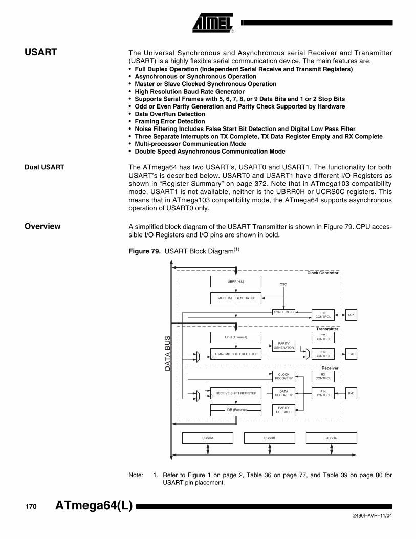
USART The Universal Synchronous and Asynchronous serial Receiver and Transmitter(USART) is a highly flexible serial communication device. The main features are:• Full Duplex Operation (Independent Serial Receive and Transmit Registers)• Asynchronous or Synchronous Operation• Master or Slave Clocked Synchronous Operation• High Resolution Baud Rate Generator• Supports Serial Frames with 5, 6, 7, 8, or 9 Data Bits and 1 or 2 Stop Bits• Odd or Even Parity Generation and Parity Check Supported by Hardware• Data OverRun Detection• Framing Error Detection• Noise Filtering Includes False Start Bit Detection and Digital Low Pass Filter• Three Separate Interrupts on TX Complete, TX Data Register Empty and RX Complete• Multi-processor Communication Mode• Double Speed Asynchronous Communication Mode
Dual USART The ATmega64 has two USART’s, USART0 and USART1. The functionality for bothUSART’s is described below. USART0 and USART1 have different I/O Registers asshown in “Register Summary” on page 372. Note that in ATmega103 compatibilitymode, USART1 is not available, neither is the UBRR0H or UCRS0C registers. Thismeans that in ATmega103 compatibility mode, the ATmega64 supports asynchronousoperation of USART0 only.
Overview A simplified block diagram of the USART Transmitter is shown in Figure 79. CPU acces-sible I/O Registers and I/O pins are shown in bold.
Figure 79. USART Block Diagram(1)
Note: 1. Refer to Figure 1 on page 2, Table 36 on page 77, and Table 39 on page 80 forUSART pin placement.
PARITYGENERATOR
UBRR[H:L]
UDR (Transmit)
UCSRA UCSRB UCSRC
BAUD RATE GENERATOR
TRANSMIT SHIFT REGISTER
RECEIVE SHIFT REGISTER RxD
TxDPIN
CONTROL
UDR (Receive)
PINCONTROL
XCK
DATARECOVERY
CLOCKRECOVERY
PINCONTROL
TXCONTROL
RXCONTROL
PARITYCHECKER
DA
TA
BU
S
OSC
SYNC LOGIC
Clock Generator
Transmitter
Receiver
170 ATmega64(L)2490I–AVR–11/04
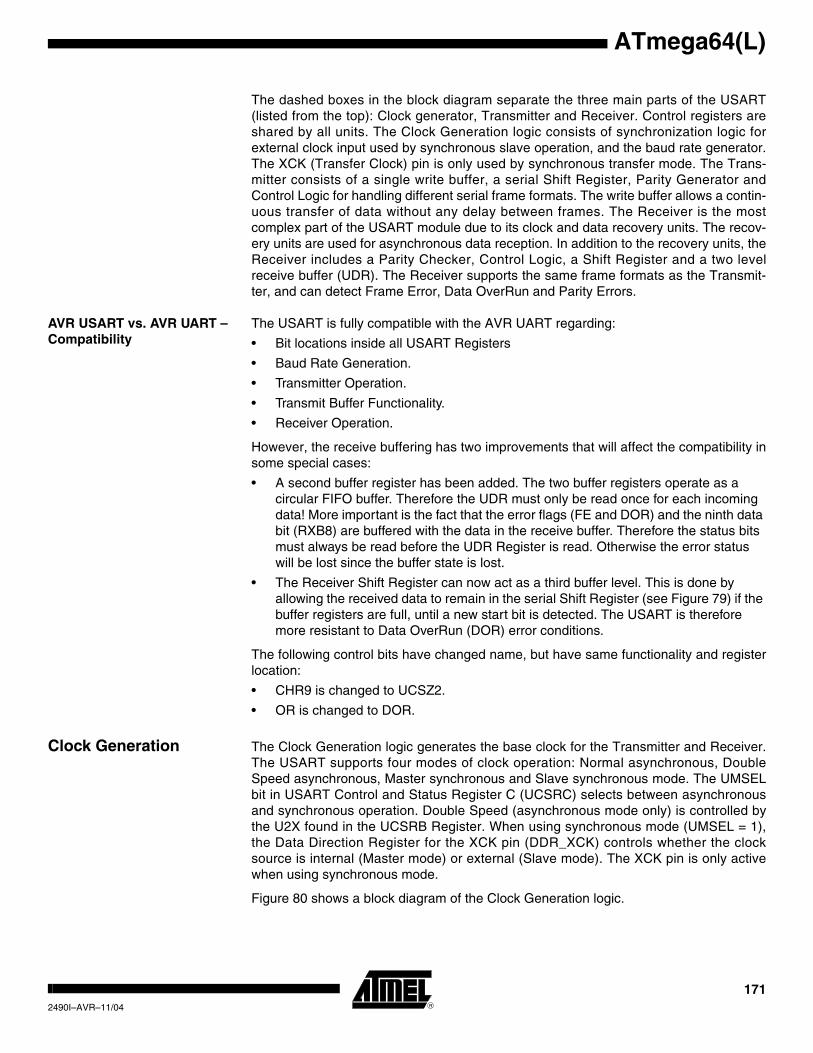
ATmega64(L)
The dashed boxes in the block diagram separate the three main parts of the USART(listed from the top): Clock generator, Transmitter and Receiver. Control registers areshared by all units. The Clock Generation logic consists of synchronization logic forexternal clock input used by synchronous slave operation, and the baud rate generator.The XCK (Transfer Clock) pin is only used by synchronous transfer mode. The Trans-mitter consists of a single write buffer, a serial Shift Register, Parity Generator andControl Logic for handling different serial frame formats. The write buffer allows a contin-uous transfer of data without any delay between frames. The Receiver is the mostcomplex part of the USART module due to its clock and data recovery units. The recov-ery units are used for asynchronous data reception. In addition to the recovery units, theReceiver includes a Parity Checker, Control Logic, a Shift Register and a two levelreceive buffer (UDR). The Receiver supports the same frame formats as the Transmit-ter, and can detect Frame Error, Data OverRun and Parity Errors.
AVR USART vs. AVR UART – Compatibility
The USART is fully compatible with the AVR UART regarding:
• Bit locations inside all USART Registers
• Baud Rate Generation.
• Transmitter Operation.
• Transmit Buffer Functionality.
• Receiver Operation.
However, the receive buffering has two improvements that will affect the compatibility insome special cases:
• A second buffer register has been added. The two buffer registers operate as a circular FIFO buffer. Therefore the UDR must only be read once for each incoming data! More important is the fact that the error flags (FE and DOR) and the ninth data bit (RXB8) are buffered with the data in the receive buffer. Therefore the status bits must always be read before the UDR Register is read. Otherwise the error status will be lost since the buffer state is lost.
• The Receiver Shift Register can now act as a third buffer level. This is done by allowing the received data to remain in the serial Shift Register (see Figure 79) if the buffer registers are full, until a new start bit is detected. The USART is therefore more resistant to Data OverRun (DOR) error conditions.
The following control bits have changed name, but have same functionality and registerlocation:
• CHR9 is changed to UCSZ2.
• OR is changed to DOR.
Clock Generation The Clock Generation logic generates the base clock for the Transmitter and Receiver.The USART supports four modes of clock operation: Normal asynchronous, DoubleSpeed asynchronous, Master synchronous and Slave synchronous mode. The UMSELbit in USART Control and Status Register C (UCSRC) selects between asynchronousand synchronous operation. Double Speed (asynchronous mode only) is controlled bythe U2X found in the UCSRB Register. When using synchronous mode (UMSEL = 1),the Data Direction Register for the XCK pin (DDR_XCK) controls whether the clocksource is internal (Master mode) or external (Slave mode). The XCK pin is only activewhen using synchronous mode.
Figure 80 shows a block diagram of the Clock Generation logic.
1712490I–AVR–11/04
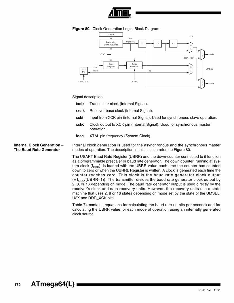
Figure 80. Clock Generation Logic, Block Diagram
Signal description:
txclk Transmitter clock (Internal Signal).
rxclk Receiver base clock (Internal Signal).
xcki Input from XCK pin (internal Signal). Used for synchronous slave operation.
xcko Clock output to XCK pin (Internal Signal). Used for synchronous masteroperation.
fosc XTAL pin frequency (System Clock).
Internal Clock Generation – The Baud Rate Generator
Internal clock generation is used for the asynchronous and the synchronous mastermodes of operation. The description in this section refers to Figure 80.
The USART Baud Rate Register (UBRR) and the down-counter connected to it functionas a programmable prescaler or baud rate generator. The down-counter, running at sys-tem clock (fOSC), is loaded with the UBRR value each time the counter has counteddown to zero or when the UBRRL Register is written. A clock is generated each time thecounter reaches zero. This clock is the baud rate generator clock output(= fOSC/(UBRR+1)). The transmitter divides the baud rate generator clock output by2, 8, or 16 depending on mode. The baud rate generator output is used directly by thereceiver’s clock and data recovery units. However, the recovery units use a statemachine that uses 2, 8 or 16 states depending on mode set by the state of the UMSEL,U2X and DDR_XCK bits.
Table 74 contains equations for calculating the baud rate (in bits per second) and forcalculating the UBRR value for each mode of operation using an internally generatedclock source.
PrescalingDown-Counter / 2
UBRR
/ 4 / 2
fosc
UBRR+1
SyncRegister
OSC
XCKPin
txclk
U2X
UMSEL
DDR_XCK
0
1
0
1
xcki
xcko
DDR_XCKrxclk
0
1
1
0Edge
Detector
UCPOL
172 ATmega64(L)2490I–AVR–11/04
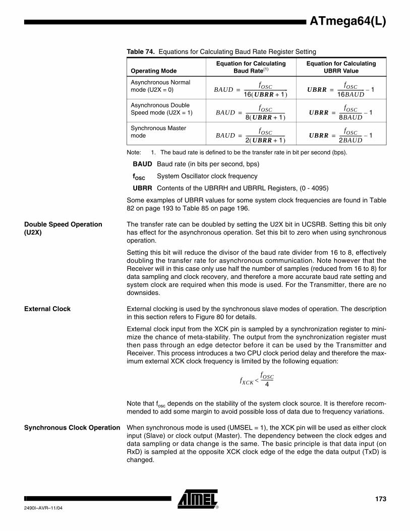
ATmega64(L)
Note: 1. The baud rate is defined to be the transfer rate in bit per second (bps).
BAUD Baud rate (in bits per second, bps)
fOSC System Oscillator clock frequency
UBRR Contents of the UBRRH and UBRRL Registers, (0 - 4095)
Some examples of UBRR values for some system clock frequencies are found in Table82 on page 193 to Table 85 on page 196.
Double Speed Operation (U2X)
The transfer rate can be doubled by setting the U2X bit in UCSRB. Setting this bit onlyhas effect for the asynchronous operation. Set this bit to zero when using synchronousoperation.
Setting this bit will reduce the divisor of the baud rate divider from 16 to 8, effectivelydoubling the transfer rate for asynchronous communication. Note however that theReceiver will in this case only use half the number of samples (reduced from 16 to 8) fordata sampling and clock recovery, and therefore a more accurate baud rate setting andsystem clock are required when this mode is used. For the Transmitter, there are nodownsides.
External Clock External clocking is used by the synchronous slave modes of operation. The descriptionin this section refers to Figure 80 for details.
External clock input from the XCK pin is sampled by a synchronization register to mini-mize the chance of meta-stability. The output from the synchronization register mustthen pass through an edge detector before it can be used by the Transmitter andReceiver. This process introduces a two CPU clock period delay and therefore the max-imum external XCK clock frequency is limited by the following equation:
Note that fosc depends on the stability of the system clock source. It is therefore recom-mended to add some margin to avoid possible loss of data due to frequency variations.
Synchronous Clock Operation When synchronous mode is used (UMSEL = 1), the XCK pin will be used as either clockinput (Slave) or clock output (Master). The dependency between the clock edges anddata sampling or data change is the same. The basic principle is that data input (onRxD) is sampled at the opposite XCK clock edge of the edge the data output (TxD) ischanged.
Table 74. Equations for Calculating Baud Rate Register Setting
Operating ModeEquation for Calculating
Baud Rate(1)Equation for Calculating
UBRR Value
Asynchronous Normal mode (U2X = 0)
Asynchronous Double Speed mode (U2X = 1)
Synchronous Master mode
BAUDfOSC
16 UBRR 1+( )---------------------------------------= UBRR
fOSC16BAUD------------------------ 1–=
BAUDfOSC
8 UBRR 1+( )-----------------------------------= UBRR
fOSC8BAUD-------------------- 1–=
BAUDfOSC
2 UBRR 1+( )-----------------------------------= UBRR
fOSC2BAUD-------------------- 1–=
fXCKfOSC
4-----------<
1732490I–AVR–11/04
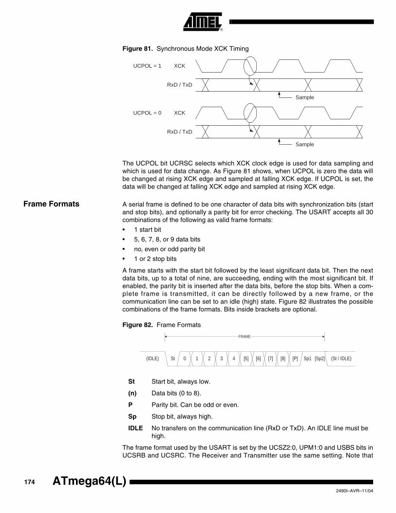
Figure 81. Synchronous Mode XCK Timing
The UCPOL bit UCRSC selects which XCK clock edge is used for data sampling andwhich is used for data change. As Figure 81 shows, when UCPOL is zero the data willbe changed at rising XCK edge and sampled at falling XCK edge. If UCPOL is set, thedata will be changed at falling XCK edge and sampled at rising XCK edge.
Frame Formats A serial frame is defined to be one character of data bits with synchronization bits (startand stop bits), and optionally a parity bit for error checking. The USART accepts all 30combinations of the following as valid frame formats:
• 1 start bit
• 5, 6, 7, 8, or 9 data bits
• no, even or odd parity bit
• 1 or 2 stop bits
A frame starts with the start bit followed by the least significant data bit. Then the nextdata bits, up to a total of nine, are succeeding, ending with the most significant bit. Ifenabled, the parity bit is inserted after the data bits, before the stop bits. When a com-plete frame is transmitted, it can be directly followed by a new frame, or thecommunication line can be set to an idle (high) state. Figure 82 illustrates the possiblecombinations of the frame formats. Bits inside brackets are optional.
Figure 82. Frame Formats
St Start bit, always low.
(n) Data bits (0 to 8).
P Parity bit. Can be odd or even.
Sp Stop bit, always high.
IDLE No transfers on the communication line (RxD or TxD). An IDLE line must behigh.
The frame format used by the USART is set by the UCSZ2:0, UPM1:0 and USBS bits inUCSRB and UCSRC. The Receiver and Transmitter use the same setting. Note that
RxD / TxD
XCK
RxD / TxD
XCKUCPOL = 0
UCPOL = 1
Sample
Sample
10 2 3 4 [5] [6] [7] [8] [P]St Sp1 [Sp2] (St / IDLE)(IDLE)
FRAME
174 ATmega64(L)2490I–AVR–11/04
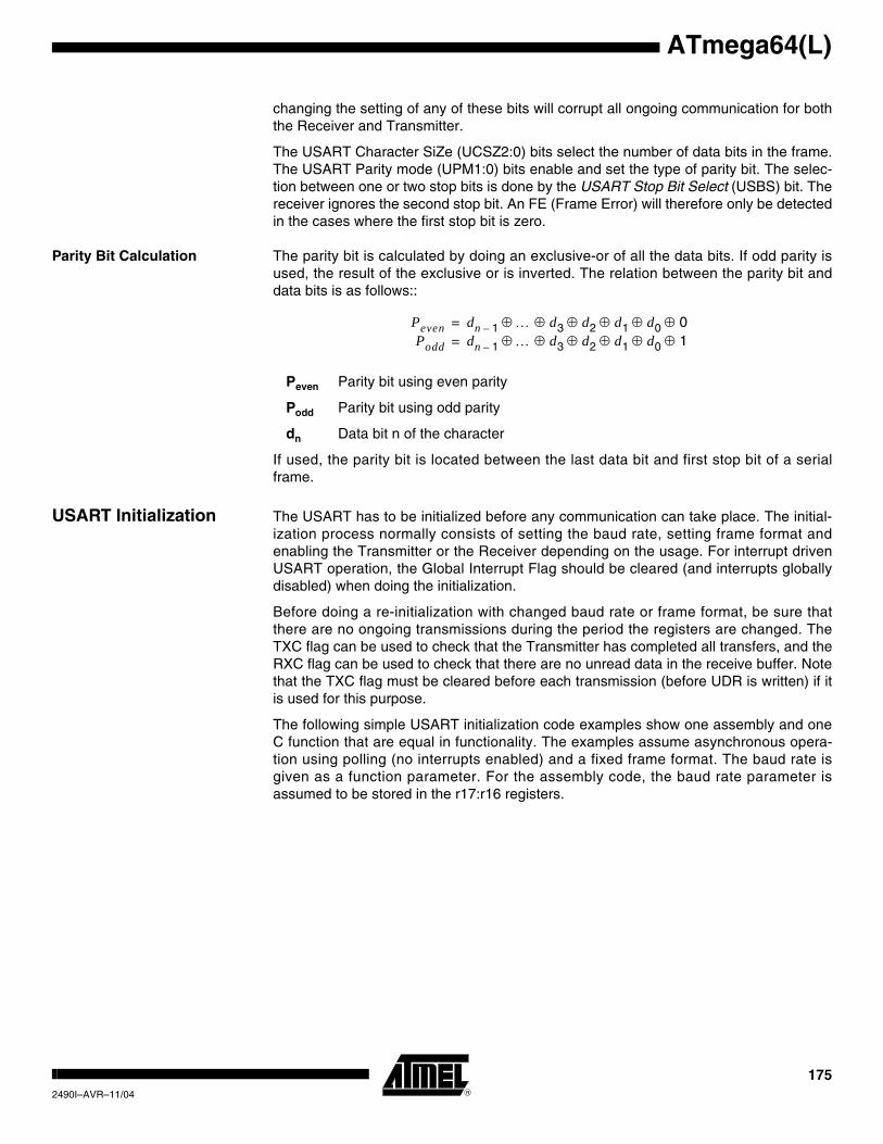
ATmega64(L)
changing the setting of any of these bits will corrupt all ongoing communication for boththe Receiver and Transmitter.
The USART Character SiZe (UCSZ2:0) bits select the number of data bits in the frame.The USART Parity mode (UPM1:0) bits enable and set the type of parity bit. The selec-tion between one or two stop bits is done by the USART Stop Bit Select (USBS) bit. Thereceiver ignores the second stop bit. An FE (Frame Error) will therefore only be detectedin the cases where the first stop bit is zero.
Parity Bit Calculation The parity bit is calculated by doing an exclusive-or of all the data bits. If odd parity isused, the result of the exclusive or is inverted. The relation between the parity bit anddata bits is as follows::
Peven Parity bit using even parity
Podd Parity bit using odd parity
dn Data bit n of the character
If used, the parity bit is located between the last data bit and first stop bit of a serialframe.
USART Initialization The USART has to be initialized before any communication can take place. The initial-ization process normally consists of setting the baud rate, setting frame format andenabling the Transmitter or the Receiver depending on the usage. For interrupt drivenUSART operation, the Global Interrupt Flag should be cleared (and interrupts globallydisabled) when doing the initialization.
Before doing a re-initialization with changed baud rate or frame format, be sure thatthere are no ongoing transmissions during the period the registers are changed. TheTXC flag can be used to check that the Transmitter has completed all transfers, and theRXC flag can be used to check that there are no unread data in the receive buffer. Notethat the TXC flag must be cleared before each transmission (before UDR is written) if itis used for this purpose.
The following simple USART initialization code examples show one assembly and oneC function that are equal in functionality. The examples assume asynchronous opera-tion using polling (no interrupts enabled) and a fixed frame format. The baud rate isgiven as a function parameter. For the assembly code, the baud rate parameter isassumed to be stored in the r17:r16 registers.
Peven dn 1– … d3 d2 d1 d0 0Podd
⊕ ⊕ ⊕ ⊕ ⊕ ⊕dn 1– … d3 d2 d1 d0 1⊕ ⊕ ⊕ ⊕ ⊕ ⊕
==
1752490I–AVR–11/04
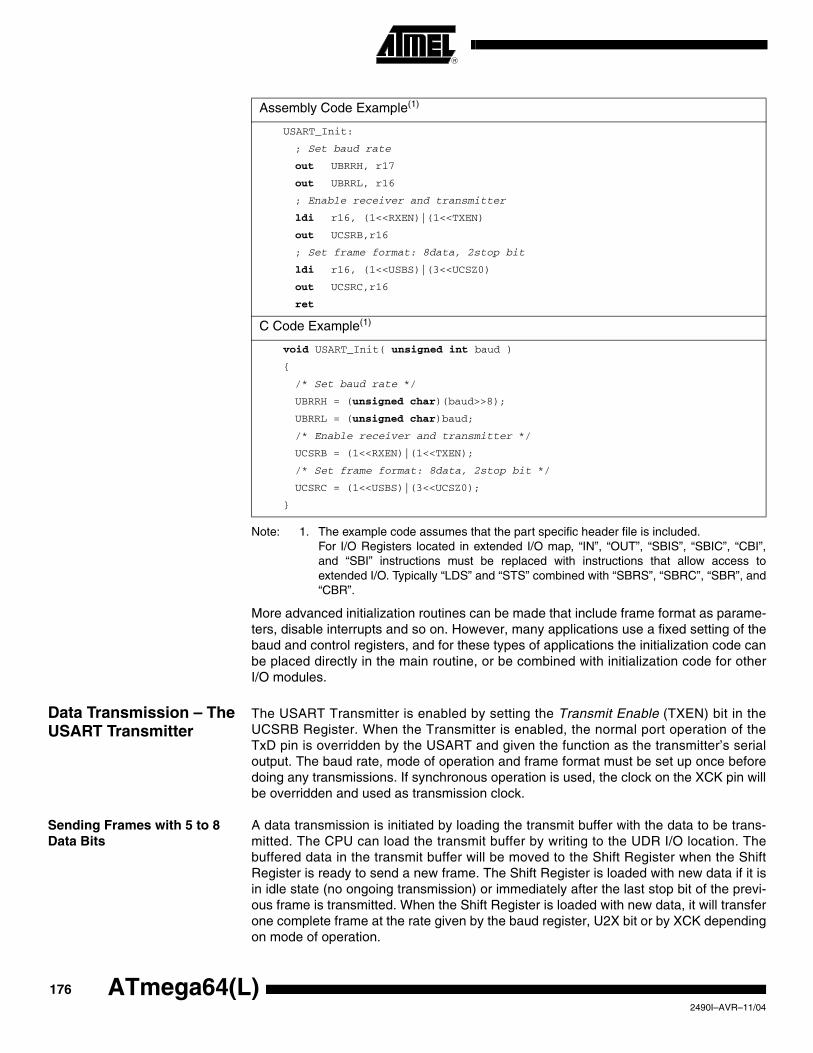
Note: 1. The example code assumes that the part specific header file is included.For I/O Registers located in extended I/O map, “IN”, “OUT”, “SBIS”, “SBIC”, “CBI”,and “SBI” instructions must be replaced with instructions that allow access toextended I/O. Typically “LDS” and “STS” combined with “SBRS”, “SBRC”, “SBR”, and“CBR”.
More advanced initialization routines can be made that include frame format as parame-ters, disable interrupts and so on. However, many applications use a fixed setting of thebaud and control registers, and for these types of applications the initialization code canbe placed directly in the main routine, or be combined with initialization code for otherI/O modules.
Data Transmission – The USART Transmitter
The USART Transmitter is enabled by setting the Transmit Enable (TXEN) bit in theUCSRB Register. When the Transmitter is enabled, the normal port operation of theTxD pin is overridden by the USART and given the function as the transmitter’s serialoutput. The baud rate, mode of operation and frame format must be set up once beforedoing any transmissions. If synchronous operation is used, the clock on the XCK pin willbe overridden and used as transmission clock.
Sending Frames with 5 to 8 Data Bits
A data transmission is initiated by loading the transmit buffer with the data to be trans-mitted. The CPU can load the transmit buffer by writing to the UDR I/O location. Thebuffered data in the transmit buffer will be moved to the Shift Register when the ShiftRegister is ready to send a new frame. The Shift Register is loaded with new data if it isin idle state (no ongoing transmission) or immediately after the last stop bit of the previ-ous frame is transmitted. When the Shift Register is loaded with new data, it will transferone complete frame at the rate given by the baud register, U2X bit or by XCK dependingon mode of operation.
Assembly Code Example(1)
USART_Init:
; Set baud rate
out UBRRH, r17
out UBRRL, r16
; Enable receiver and transmitter
ldi r16, (1<<RXEN)|(1<<TXEN)
out UCSRB,r16
; Set frame format: 8data, 2stop bit
ldi r16, (1<<USBS)|(3<<UCSZ0)
out UCSRC,r16
ret
C Code Example(1)
void USART_Init( unsigned int baud )
/* Set baud rate */
UBRRH = (unsigned char)(baud>>8);
UBRRL = (unsigned char)baud;
/* Enable receiver and transmitter */
UCSRB = (1<<RXEN)|(1<<TXEN);
/* Set frame format: 8data, 2stop bit */
UCSRC = (1<<USBS)|(3<<UCSZ0);
176 ATmega64(L)2490I–AVR–11/04
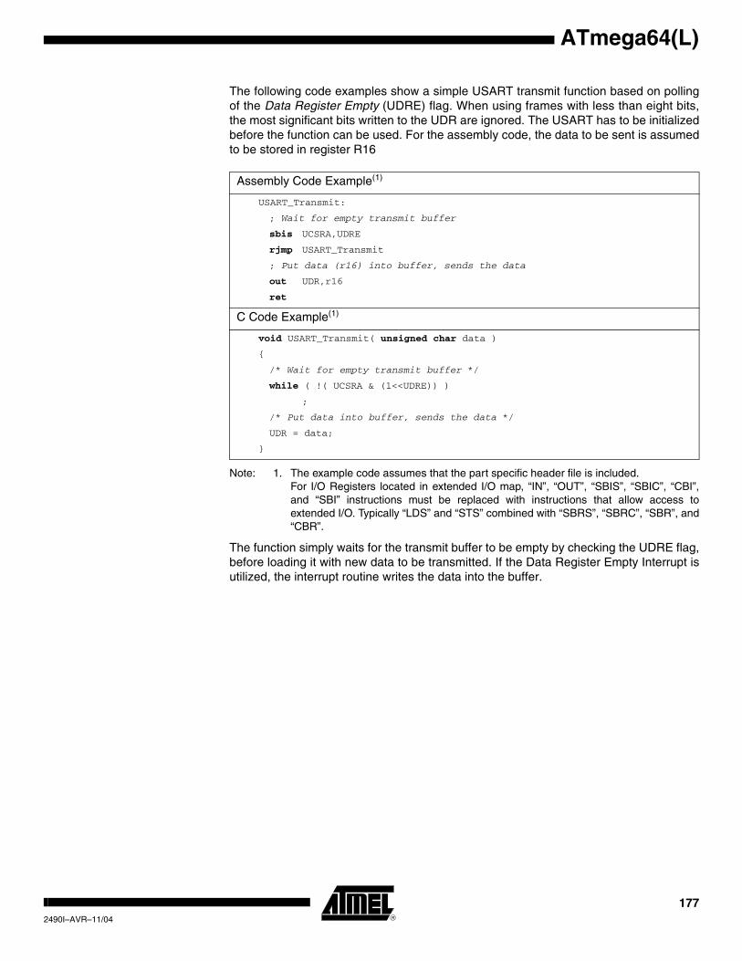
ATmega64(L)
The following code examples show a simple USART transmit function based on pollingof the Data Register Empty (UDRE) flag. When using frames with less than eight bits,the most significant bits written to the UDR are ignored. The USART has to be initializedbefore the function can be used. For the assembly code, the data to be sent is assumedto be stored in register R16
Note: 1. The example code assumes that the part specific header file is included.For I/O Registers located in extended I/O map, “IN”, “OUT”, “SBIS”, “SBIC”, “CBI”,and “SBI” instructions must be replaced with instructions that allow access toextended I/O. Typically “LDS” and “STS” combined with “SBRS”, “SBRC”, “SBR”, and“CBR”.
The function simply waits for the transmit buffer to be empty by checking the UDRE flag,before loading it with new data to be transmitted. If the Data Register Empty Interrupt isutilized, the interrupt routine writes the data into the buffer.
Assembly Code Example(1)
USART_Transmit:
; Wait for empty transmit buffer
sbis UCSRA,UDRE
rjmp USART_Transmit
; Put data (r16) into buffer, sends the data
out UDR,r16
ret
C Code Example(1)
void USART_Transmit( unsigned char data )
/* Wait for empty transmit buffer */
while ( !( UCSRA & (1<<UDRE)) )
;
/* Put data into buffer, sends the data */
UDR = data;
1772490I–AVR–11/04
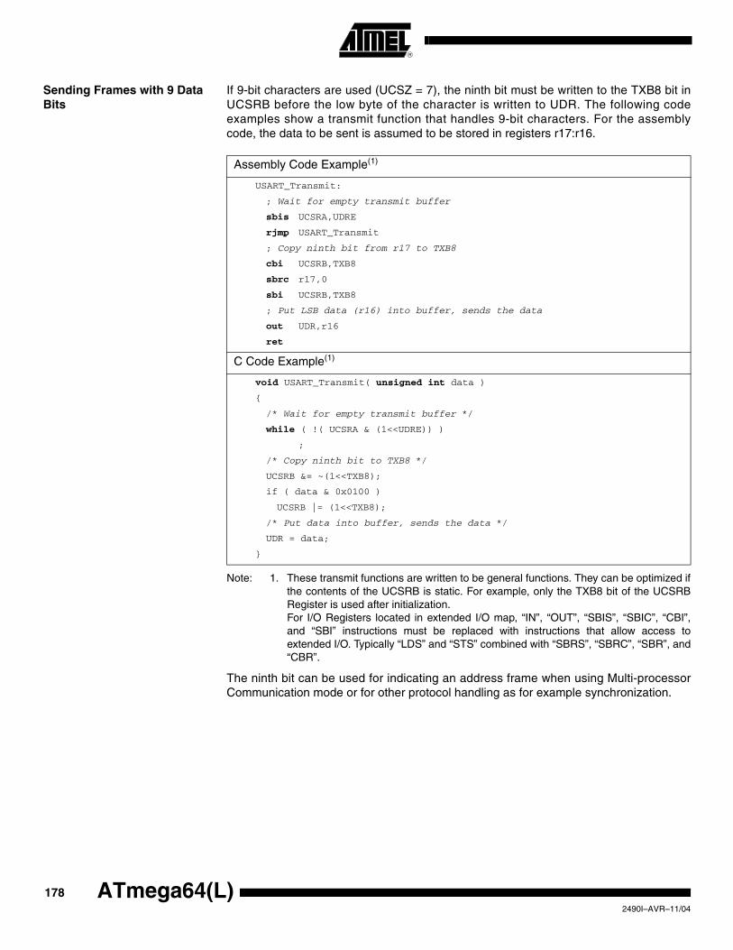
Sending Frames with 9 Data Bits
If 9-bit characters are used (UCSZ = 7), the ninth bit must be written to the TXB8 bit inUCSRB before the low byte of the character is written to UDR. The following codeexamples show a transmit function that handles 9-bit characters. For the assemblycode, the data to be sent is assumed to be stored in registers r17:r16.
Note: 1. These transmit functions are written to be general functions. They can be optimized ifthe contents of the UCSRB is static. For example, only the TXB8 bit of the UCSRBRegister is used after initialization.For I/O Registers located in extended I/O map, “IN”, “OUT”, “SBIS”, “SBIC”, “CBI”,and “SBI” instructions must be replaced with instructions that allow access toextended I/O. Typically “LDS” and “STS” combined with “SBRS”, “SBRC”, “SBR”, and“CBR”.
The ninth bit can be used for indicating an address frame when using Multi-processorCommunication mode or for other protocol handling as for example synchronization.
Assembly Code Example(1)
USART_Transmit:
; Wait for empty transmit buffer
sbis UCSRA,UDRE
rjmp USART_Transmit
; Copy ninth bit from r17 to TXB8
cbi UCSRB,TXB8
sbrc r17,0
sbi UCSRB,TXB8
; Put LSB data (r16) into buffer, sends the data
out UDR,r16
ret
C Code Example(1)
void USART_Transmit( unsigned int data )
/* Wait for empty transmit buffer */
while ( !( UCSRA & (1<<UDRE)) )
;
/* Copy ninth bit to TXB8 */
UCSRB &= ~(1<<TXB8);
if ( data & 0x0100 )
UCSRB |= (1<<TXB8);
/* Put data into buffer, sends the data */
UDR = data;
178 ATmega64(L)2490I–AVR–11/04
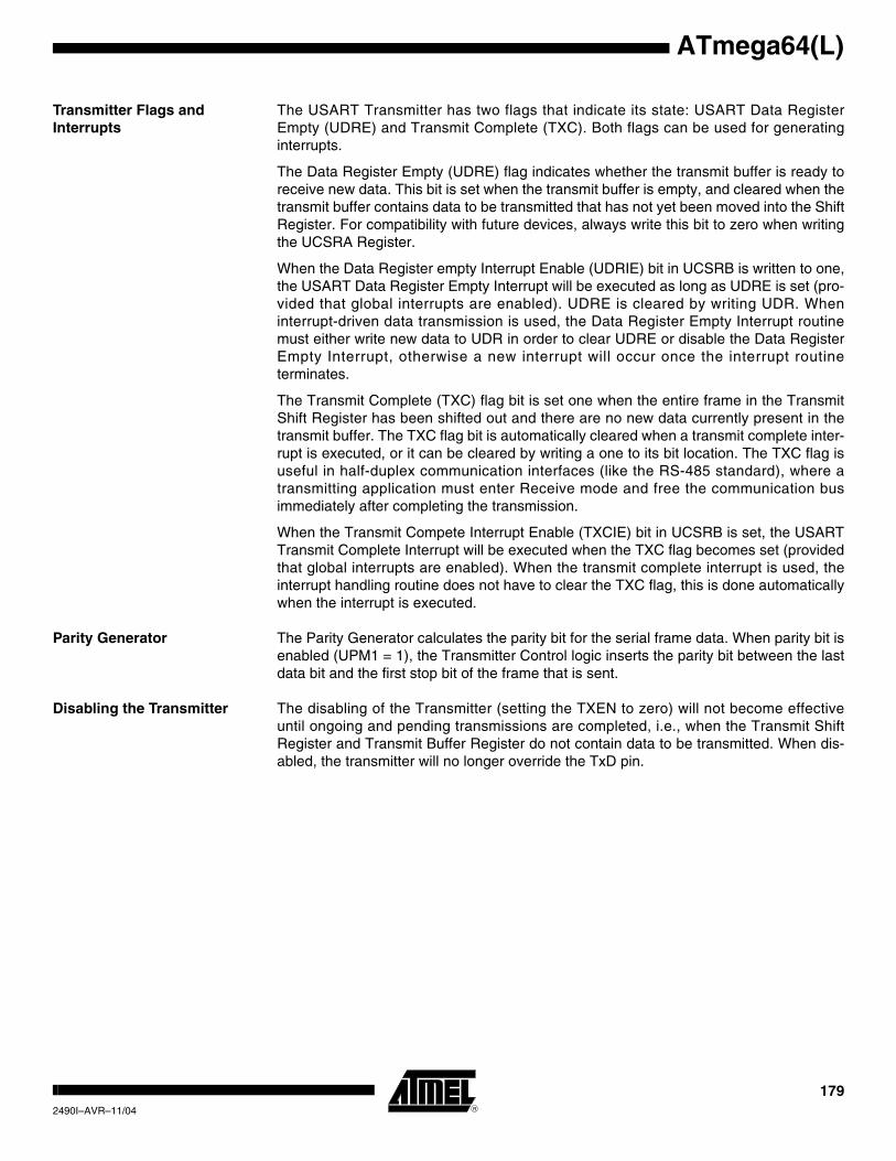
ATmega64(L)
Transmitter Flags and Interrupts
The USART Transmitter has two flags that indicate its state: USART Data RegisterEmpty (UDRE) and Transmit Complete (TXC). Both flags can be used for generatinginterrupts.
The Data Register Empty (UDRE) flag indicates whether the transmit buffer is ready toreceive new data. This bit is set when the transmit buffer is empty, and cleared when thetransmit buffer contains data to be transmitted that has not yet been moved into the ShiftRegister. For compatibility with future devices, always write this bit to zero when writingthe UCSRA Register.
When the Data Register empty Interrupt Enable (UDRIE) bit in UCSRB is written to one,the USART Data Register Empty Interrupt will be executed as long as UDRE is set (pro-vided that global interrupts are enabled). UDRE is cleared by writing UDR. Wheninterrupt-driven data transmission is used, the Data Register Empty Interrupt routinemust either write new data to UDR in order to clear UDRE or disable the Data RegisterEmpty Interrupt, otherwise a new interrupt will occur once the interrupt routineterminates.
The Transmit Complete (TXC) flag bit is set one when the entire frame in the TransmitShift Register has been shifted out and there are no new data currently present in thetransmit buffer. The TXC flag bit is automatically cleared when a transmit complete inter-rupt is executed, or it can be cleared by writing a one to its bit location. The TXC flag isuseful in half-duplex communication interfaces (like the RS-485 standard), where atransmitting application must enter Receive mode and free the communication busimmediately after completing the transmission.
When the Transmit Compete Interrupt Enable (TXCIE) bit in UCSRB is set, the USARTTransmit Complete Interrupt will be executed when the TXC flag becomes set (providedthat global interrupts are enabled). When the transmit complete interrupt is used, theinterrupt handling routine does not have to clear the TXC flag, this is done automaticallywhen the interrupt is executed.
Parity Generator The Parity Generator calculates the parity bit for the serial frame data. When parity bit isenabled (UPM1 = 1), the Transmitter Control logic inserts the parity bit between the lastdata bit and the first stop bit of the frame that is sent.
Disabling the Transmitter The disabling of the Transmitter (setting the TXEN to zero) will not become effectiveuntil ongoing and pending transmissions are completed, i.e., when the Transmit ShiftRegister and Transmit Buffer Register do not contain data to be transmitted. When dis-abled, the transmitter will no longer override the TxD pin.
1792490I–AVR–11/04
Data Reception – The USART Receiver
The USART Receiver is enabled by writing the Receive Enable (RXEN) bit in theUCSRB Register to one. When the Receiver is enabled, the normal pin operation of theRxD pin is overridden by the USART and given the function as the receiver’s serialinput. The baud rate, mode of operation and frame format must be set up once beforeany serial reception can be done. If synchronous operation is used, the clock on theXCK pin will be used as transfer clock.
Receiving Frames with 5 to 8 Data Bits
The Receiver starts data reception when it detects a valid start bit. Each bit that followsthe start bit will be sampled at the baud rate or XCK clock, and shifted into the ReceiveShift Register until the first stop bit of a frame is received. A second stop bit will beignored by the Receiver. When the first stop bit is received, i.e., a complete serial frameis present in the Receive Shift Register, the contents of the Shift Register will be movedinto the receive buffer. The receive buffer can then be read by reading the UDR I/Olocation.
The following code example shows a simple USART receive function based on pollingof the Receive Complete (RXC) flag. When using frames with less than eight bits themost significant bits of the data read from the UDR will be masked to zero. The USARThas to be initialized before the function can be used.
Note: 1. The example code assumes that the part specific header file is included.For I/O Registers located in extended I/O map, “IN”, “OUT”, “SBIS”, “SBIC”, “CBI”,and “SBI” instructions must be replaced with instructions that allow access toextended I/O. Typically “LDS” and “STS” combined with “SBRS”, “SBRC”, “SBR”, and“CBR”.
The function simply waits for data to be present in the receive buffer by checking theRXC flag, before reading the buffer and returning the value.
Assembly Code Example(1)
USART_Receive:
; Wait for data to be received
sbis UCSRA, RXC
rjmp USART_Receive
; Get and return received data from buffer
in r16, UDR
ret
C Code Example(1)
unsigned char USART_Receive( void )
/* Wait for data to be received */
while ( !(UCSRA & (1<<RXC)) )
;
/* Get and return received data from buffer */
return UDR;
180 ATmega64(L)2490I–AVR–11/04
ATmega64(L)
Receiving Frames with 9 Data Bits
If 9-bit characters are used (UCSZ=7) the ninth bit must be read from the RXB8 bit inUCSRB before reading the low bits from the UDR. This rule applies to the FE, DOR,and UPE status flags as well. Read status from UCSRA, then data from UDR. Readingthe UDR I/O location will change the state of the receive buffer FIFO and consequentlythe TXB8, FE, DOR, and UPE bits, which all are stored in the FIFO, will change. The fol-lowing code example shows a simple USART receive function that handles both nine bitcharacters and the status bits.
Note: 1. The code assumes that the part specific header file is included. For I/O Registerslocated in extended I/O map, “IN”, “OUT”, “SBIS”, “SBIC”, “CBI”, and “SBI” instruc-
Assembly Code Example(1)
USART_Receive:
; Wait for data to be received
sbis UCSRA, RXC
rjmp USART_Receive
; Get status and ninth bit, then data from buffer
in r18, UCSRA
in r17, UCSRB
in r16, UDR
; If error, return -1
andi r18,(1<<FE)|(1<<DOR)|(1<<UPE)
breq USART_ReceiveNoError
ldi r17, HIGH(-1)
ldi r16, LOW(-1)
USART_ReceiveNoError:
; Filter the ninth bit, then return
lsr r17
andi r17, 0x01
ret
C Code Example(1)
unsigned int USART_Receive( void )
unsigned char status, resh, resl;
/* Wait for data to be received */
while ( !(UCSRA & (1<<RXC)) )
;
/* Get status and ninth bit, then data */
/* from buffer */
status = UCSRA;
resh = UCSRB;
resl = UDR;
/* If error, return -1 */
if ( status & (1<<FE)|(1<<DOR)|(1<<UPE) )
return -1;
/* Filter the ninth bit, then return */
resh = (resh >> 1) & 0x01;
return ((resh << 8) | resl);
1812490I–AVR–11/04
tions must be replaced with instructions that allow access to extended I/O. Typically“LDS” and “STS” combined with “SBRS”, “SBRC”, “SBR”, and “CBR”.
The receive function example reads all the I/O Registers into the Register File beforeany computation is done. This gives an optimal receive buffer utilization since the bufferlocation read will be free to accept new data as early as possible.
Receive Compete Flag and Interrupt
The USART Receiver has one flag that indicates the receiver state.
The Receive Complete (RXC) flag indicates if there are unread data present in thereceive buffer. This flag is one when unread data exist in the receive buffer, and zerowhen the receive buffer is empty (i.e. does not contain any unread data). If the receiveris disabled (RXEN = 0), the receive buffer will be flushed and consequently the RXC bitwill become zero.
When the Receive Complete Interrupt Enable (RXCIE) in UCSRB is set, the USARTReceive Complete Interrupt will be executed as long as the RXC flag is set (providedthat global interrupts are enabled). When interrupt-driven data reception is used, thereceive complete routine must read the received data from UDR in order to clear theRXC flag, otherwise a new interrupt will occur once the interrupt routine terminates.
Receiver Error Flags The USART Receiver has three error flags: Frame Error (FE), Data OverRun (DOR) andUSART Parity Error (UPE). All can be accessed by reading UCSRA. Common for theerror flags is that they are located in the receive buffer together with the frame for whichthey indicate the error status. Due to the buffering of the error flags, the UCSRA must beread before the receive buffer (UDR), since reading the UDR I/O location changes thebuffer read location. Another equality for the error flags is that they can not be altered bysoftware doing a write to the flag location. However, all flags must be set to zero whenthe UCSRA is written for upward compatibility of future USART implementations. Noneof the error flags can generate interrupts.
The Frame Error (FE) flag indicates the state of the first stop bit of the next readableframe stored in the receive buffer. The FE flag is zero when the stop bit was correctlyread (as one), and the FE flag will be one when the stop bit was incorrect (zero). Thisflag can be used for detecting out-of-sync conditions, detecting break conditions andprotocol handling. The FE flag is not affected by the setting of the USBS bit in UCSRCsince the Receiver ignores all, except for the first, stop bits. For compatibility with futuredevices, always set this bit to zero when writing to UCSRA.
The Data OverRun (DOR) flag indicates data loss due to a receiver buffer full condition.A Data OverRun occurs when the receive buffer is full (two characters), it is a new char-acter waiting in the Receive Shift Register, and a new start bit is detected. If the DORflag is set there was one or more serial frame lost between the frame last read fromUDR, and the next frame read from UDR. For compatibility with future devices, alwayswrite this bit to zero when writing to UCSRA. The DOR flag is cleared when the framereceived was successfully moved from the Shift Register to the receive buffer.
The USART Parity Error (UPE) flag indicates that the next frame in the receive bufferhad a Parity Error when received. If parity check is not enabled the UPE bit will alwaysbe read zero. For compatibility with future devices, always set this bit to zero when writ-ing to UCSRA. For more details see “Parity Bit Calculation” on page 175 and “ParityChecker” on page 182.
Parity Checker The Parity Checker is active when the high USART Parity mode (UPM1) bit is set. Typeof parity check to be performed (odd or even) is selected by the UPM0 bit. Whenenabled, the Parity Checker calculates the parity of the data bits in incoming frames andcompares the result with the parity bit from the serial frame. The result of the check is
182 ATmega64(L)2490I–AVR–11/04
ATmega64(L)
stored in the receive buffer together with the received data and stop bits. The ParityError (UPE) flag can then be read by software to check if the frame had a Parity Error.
The UPE bit is set if the next character that can be read from the receive buffer had aParity Error when received and the parity checking was enabled at that point(UPM1 = 1). This bit is valid until the receive buffer (UDR) is read.
Disabling the Receiver In contrast to the Transmitter, disabling of the Receiver will be immediate. Data fromongoing receptions will therefore be lost. When disabled (i.e. the RXEN is set to zero)the receiver will no longer override the normal function of the RxD port pin. The receiverbuffer FIFO will be flushed when the Receiver is disabled. Remaining data in the bufferwill be lost
Flushing the Receive Buffer The receiver buffer FIFO will be flushed when the Receiver is disabled, i.e., the bufferwill be emptied of its contents. Unread data will be lost. If the buffer has to be flushedduring normal operation, due to for instance an error condition, read the UDR I/O loca-tion until the RXC flag is cleared. The following code examples show how to flush thereceive buffer.
Note: 1. The example code assumes that the part specific header file is included.For I/O Registers located in extended I/O map, “IN”, “OUT”, “SBIS”, “SBIC”, “CBI”,and “SBI” instructions must be replaced with instructions that allow access toextended I/O. Typically “LDS” and “STS” combined with “SBRS”, “SBRC”, “SBR”, and“CBR”.
Asynchronous Data Reception
The USART includes a clock recovery and a data recovery unit for handling asynchro-nous data reception. The clock recovery logic is used for synchronizing the internallygenerated baud rate clock to the incoming asynchronous serial frames at the RxD pin.The data recovery logic samples and low pass filters each incoming bit, thereby improv-ing the noise immunity of the Receiver. The asynchronous reception operational rangedepends on the accuracy of the internal baud rate clock, the rate of the incomingframes, and the frame size in number of bits.
Asynchronous Clock Recovery
The Clock Recovery logic synchronizes internal clock to the incoming serial frames. Fig-ure 83 illustrates the sampling process of the start bit of an incoming frame. The samplerate is 16 times the baud rate for Normal mode, and eight times the baud rate for DoubleSpeed mode. The horizontal arrows illustrate the synchronization variation due to thesampling process. Note the larger time variation when using the Double Speed mode
Assembly Code Example(1)
USART_Flush:
sbis UCSRA, RXC
ret
in r16, UDR
rjmp USART_Flush
C Code Example(1)
void USART_Flush( void )
unsigned char dummy;
while ( UCSRA & (1<<RXC) ) dummy = UDR;
1832490I–AVR–11/04
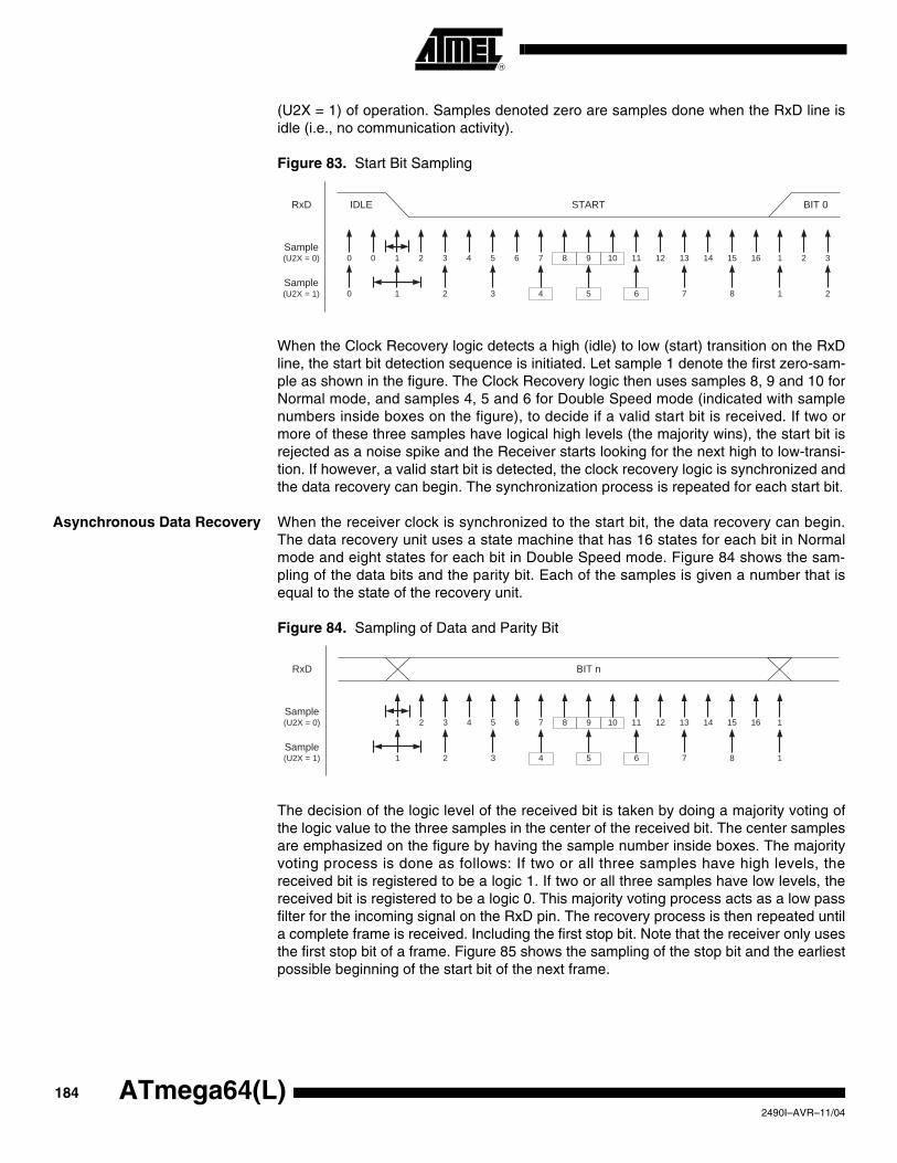
(U2X = 1) of operation. Samples denoted zero are samples done when the RxD line isidle (i.e., no communication activity).
Figure 83. Start Bit Sampling
When the Clock Recovery logic detects a high (idle) to low (start) transition on the RxDline, the start bit detection sequence is initiated. Let sample 1 denote the first zero-sam-ple as shown in the figure. The Clock Recovery logic then uses samples 8, 9 and 10 forNormal mode, and samples 4, 5 and 6 for Double Speed mode (indicated with samplenumbers inside boxes on the figure), to decide if a valid start bit is received. If two ormore of these three samples have logical high levels (the majority wins), the start bit isrejected as a noise spike and the Receiver starts looking for the next high to low-transi-tion. If however, a valid start bit is detected, the clock recovery logic is synchronized andthe data recovery can begin. The synchronization process is repeated for each start bit.
Asynchronous Data Recovery When the receiver clock is synchronized to the start bit, the data recovery can begin.The data recovery unit uses a state machine that has 16 states for each bit in Normalmode and eight states for each bit in Double Speed mode. Figure 84 shows the sam-pling of the data bits and the parity bit. Each of the samples is given a number that isequal to the state of the recovery unit.
Figure 84. Sampling of Data and Parity Bit
The decision of the logic level of the received bit is taken by doing a majority voting ofthe logic value to the three samples in the center of the received bit. The center samplesare emphasized on the figure by having the sample number inside boxes. The majorityvoting process is done as follows: If two or all three samples have high levels, thereceived bit is registered to be a logic 1. If two or all three samples have low levels, thereceived bit is registered to be a logic 0. This majority voting process acts as a low passfilter for the incoming signal on the RxD pin. The recovery process is then repeated untila complete frame is received. Including the first stop bit. Note that the receiver only usesthe first stop bit of a frame. Figure 85 shows the sampling of the stop bit and the earliestpossible beginning of the start bit of the next frame.
1 2 3 4 5 6 7 8 9 10 11 12 13 14 15 16 1 2
STARTIDLE
00
BIT 0
3
1 2 3 4 5 6 7 8 1 20
RxD
Sample(U2X = 0)
Sample(U2X = 1)
1 2 3 4 5 6 7 8 9 10 11 12 13 14 15 16 1
BIT n
1 2 3 4 5 6 7 8 1
RxD
Sample(U2X = 0)
Sample(U2X = 1)
184 ATmega64(L)2490I–AVR–11/04
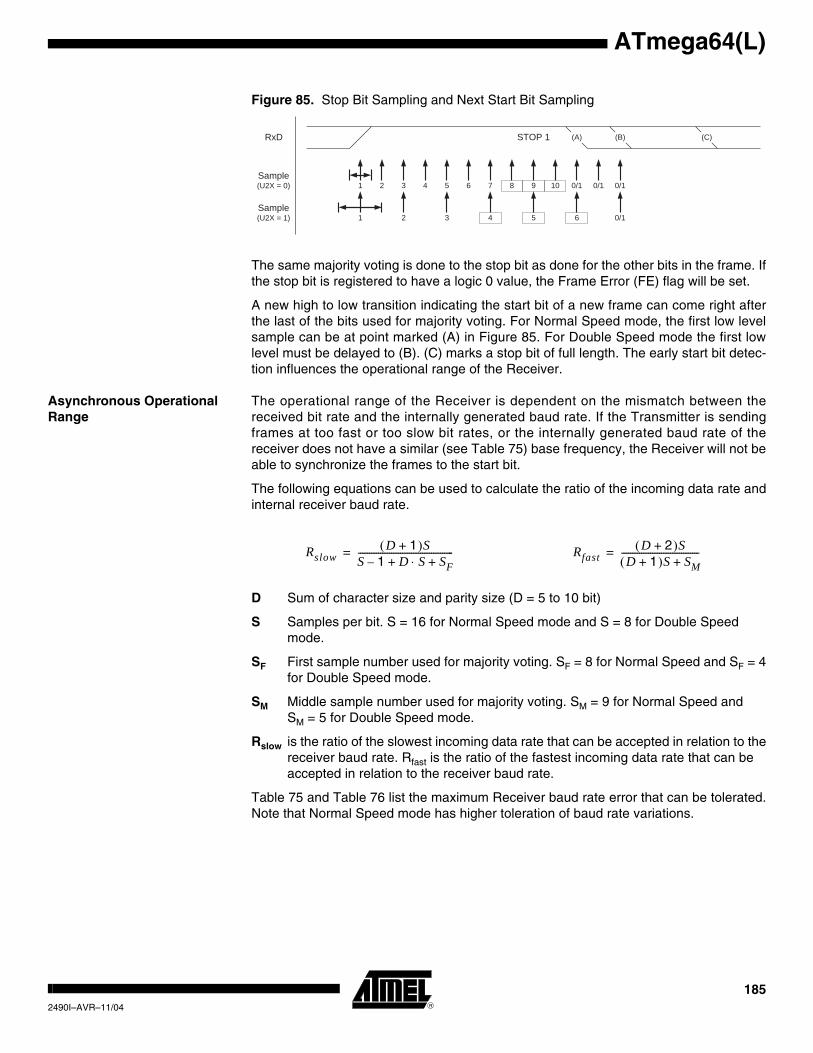
ATmega64(L)
Figure 85. Stop Bit Sampling and Next Start Bit Sampling
The same majority voting is done to the stop bit as done for the other bits in the frame. Ifthe stop bit is registered to have a logic 0 value, the Frame Error (FE) flag will be set.
A new high to low transition indicating the start bit of a new frame can come right afterthe last of the bits used for majority voting. For Normal Speed mode, the first low levelsample can be at point marked (A) in Figure 85. For Double Speed mode the first lowlevel must be delayed to (B). (C) marks a stop bit of full length. The early start bit detec-tion influences the operational range of the Receiver.
Asynchronous Operational Range
The operational range of the Receiver is dependent on the mismatch between thereceived bit rate and the internally generated baud rate. If the Transmitter is sendingframes at too fast or too slow bit rates, or the internally generated baud rate of thereceiver does not have a similar (see Table 75) base frequency, the Receiver will not beable to synchronize the frames to the start bit.
The following equations can be used to calculate the ratio of the incoming data rate andinternal receiver baud rate.
D Sum of character size and parity size (D = 5 to 10 bit)
S Samples per bit. S = 16 for Normal Speed mode and S = 8 for Double Speedmode.
SF First sample number used for majority voting. SF = 8 for Normal Speed and SF = 4for Double Speed mode.
SM Middle sample number used for majority voting. SM = 9 for Normal Speed and SM = 5 for Double Speed mode.
Rslow is the ratio of the slowest incoming data rate that can be accepted in relation to thereceiver baud rate. Rfast is the ratio of the fastest incoming data rate that can beaccepted in relation to the receiver baud rate.
Table 75 and Table 76 list the maximum Receiver baud rate error that can be tolerated.Note that Normal Speed mode has higher toleration of baud rate variations.
1 2 3 4 5 6 7 8 9 10 0/1 0/1 0/1
STOP 1
1 2 3 4 5 6 0/1
RxD
Sample(U2X = 0)
Sample(U2X = 1)
(A) (B) (C)
RslowD 1+( )S
S 1– D S⋅ SF+ +-------------------------------------------= Rfast
D 2+( )SD 1+( )S SM+
-----------------------------------=
1852490I–AVR–11/04
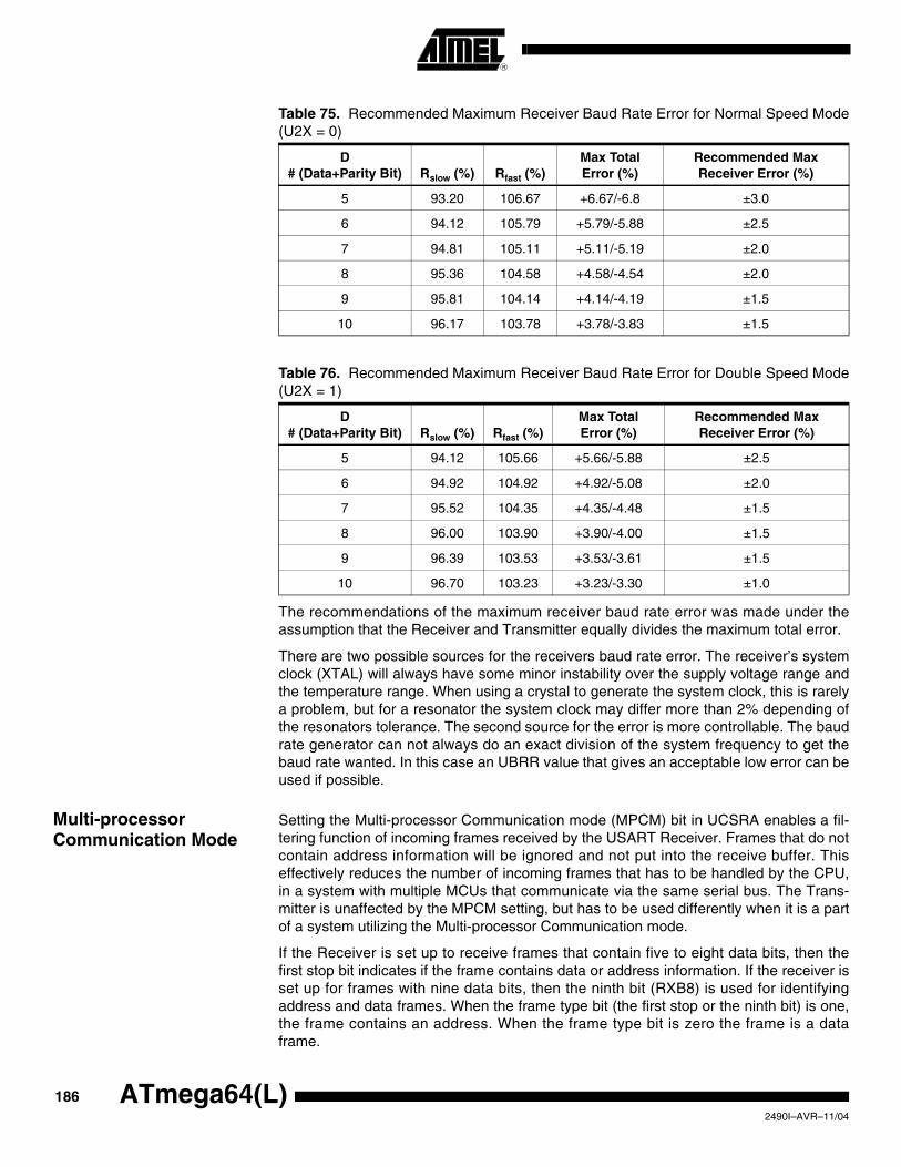
The recommendations of the maximum receiver baud rate error was made under theassumption that the Receiver and Transmitter equally divides the maximum total error.
There are two possible sources for the receivers baud rate error. The receiver’s systemclock (XTAL) will always have some minor instability over the supply voltage range andthe temperature range. When using a crystal to generate the system clock, this is rarelya problem, but for a resonator the system clock may differ more than 2% depending ofthe resonators tolerance. The second source for the error is more controllable. The baudrate generator can not always do an exact division of the system frequency to get thebaud rate wanted. In this case an UBRR value that gives an acceptable low error can beused if possible.
Multi-processor Communication Mode
Setting the Multi-processor Communication mode (MPCM) bit in UCSRA enables a fil-tering function of incoming frames received by the USART Receiver. Frames that do notcontain address information will be ignored and not put into the receive buffer. Thiseffectively reduces the number of incoming frames that has to be handled by the CPU,in a system with multiple MCUs that communicate via the same serial bus. The Trans-mitter is unaffected by the MPCM setting, but has to be used differently when it is a partof a system utilizing the Multi-processor Communication mode.
If the Receiver is set up to receive frames that contain five to eight data bits, then thefirst stop bit indicates if the frame contains data or address information. If the receiver isset up for frames with nine data bits, then the ninth bit (RXB8) is used for identifyingaddress and data frames. When the frame type bit (the first stop or the ninth bit) is one,the frame contains an address. When the frame type bit is zero the frame is a dataframe.
Table 75. Recommended Maximum Receiver Baud Rate Error for Normal Speed Mode(U2X = 0)
D# (Data+Parity Bit) Rslow (%) Rfast (%)
Max Total Error (%)
Recommended Max Receiver Error (%)
5 93.20 106.67 +6.67/-6.8 ±3.0
6 94.12 105.79 +5.79/-5.88 ±2.5
7 94.81 105.11 +5.11/-5.19 ±2.0
8 95.36 104.58 +4.58/-4.54 ±2.0
9 95.81 104.14 +4.14/-4.19 ±1.5
10 96.17 103.78 +3.78/-3.83 ±1.5
Table 76. Recommended Maximum Receiver Baud Rate Error for Double Speed Mode(U2X = 1)
D# (Data+Parity Bit) Rslow (%) Rfast (%)
Max Total Error (%)
Recommended Max Receiver Error (%)
5 94.12 105.66 +5.66/-5.88 ±2.5
6 94.92 104.92 +4.92/-5.08 ±2.0
7 95.52 104.35 +4.35/-4.48 ±1.5
8 96.00 103.90 +3.90/-4.00 ±1.5
9 96.39 103.53 +3.53/-3.61 ±1.5
10 96.70 103.23 +3.23/-3.30 ±1.0
186 ATmega64(L)2490I–AVR–11/04
ATmega64(L)
The Multi-processor Communication mode enables several Slave MCUs to receive datafrom a Master MCU. This is done by first decoding an address frame to find out whichMCU has been addressed. If a particular Slave MCU has been addressed, it will receivethe following data frames as normal, while the other slave MCUs will ignore the receivedframes until another address frame is received.
Using MPCM For an MCU to act as a Master MCU, it can use a 9-bit character frame format(UCSZ = 7). The ninth bit (TXB8) must be set when an address frame (TXB8 = 1) orcleared when a data frame (TXB = 0) is being transmitted. The Slave MCUs must in thiscase be set to use a 9-bit character frame format.
The following procedure should be used to exchange data in Multi-processor Communi-cation mode:
1. All Slave MCUs are in Multi-processor Communication mode (MPCM in UCSRA is set).
2. The Master MCU sends an address frame, and all slaves receive and read this frame. In the Slave MCUs, the RXC flag in UCSRA will be set as normal.
3. Each Slave MCU reads the UDR Register and determines if it has been selected. If so, it clears the MPCM bit in UCSRA, otherwise it waits for the next address byte and keeps the MPCM setting.
4. The addressed MCU will receive all data frames until a new address frame is received. The other Slave MCUs, which still have the MPCM bit set, will ignore the data frames.
5. When the last data frame is received by the addressed MCU, the addressed MCU sets the MPCM bit and waits for a new address frame from Master. The process then repeats from 2.
Using any of the 5- to 8-bit character frame formats is possible, but impractical since theReceiver must change between using n and n+1 character frame formats. This makesfull duplex operation difficult since the Transmitter and Receiver uses the same charac-ter size setting. If 5- to 8-bit character frames are used, the Transmitter must be set touse two stop bit (USBS = 1) since the first stop bit is used for indicating the frame type.
Do not use Read-Modify-Write instructions (SBI and CBI) to set or clear the MPCM bit.The MPCM bit shares the same I/O location as the TXC flag and this might accidentallybe cleared when using SBI or CBI instructions.
USART Register Description
USART I/O Data Register – UDR
The USART Transmit Data Buffer Register and USART Receive Data Buffer Registersshare the same I/O address referred to as USART Data Register or UDR. The TransmitData Buffer Register (TXB) will be the destination for data written to the UDR Registerlocation. Reading the UDR Register location will return the contents of the Receive DataBuffer Register (RXB).
For 5-, 6-, or 7-bit characters the upper unused bits will be ignored by the Transmitterand set to zero by the Receiver.
Bit 7 6 5 4 3 2 1 0
RXB[7:0] UDR (Read)TXB[7:0] UDR (Write)
Read/Write R/W R/W R/W R/W R/W R/W R/W R/W
Initial Value 0 0 0 0 0 0 0 0
1872490I–AVR–11/04
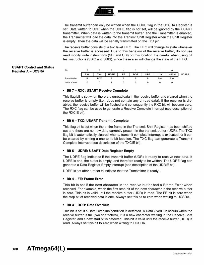
The transmit buffer can only be written when the UDRE flag in the UCSRA Register isset. Data written to UDR when the UDRE flag is not set, will be ignored by the USARTtransmitter. When data is written to the transmit buffer, and the Transmitter is enabled,the Transmitter will load the data into the Transmit Shift Register when the Shift Registeris empty. Then the data will be serially transmitted on the TxD pin.
The receive buffer consists of a two level FIFO. The FIFO will change its state wheneverthe receive buffer is accessed. Due to this behavior of the receive buffer, do not useread modify write instructions (SBI and CBI) on this location. Be careful when using bittest instructions (SBIC and SBIS), since these also will change the state of the FIFO.
USART Control and Status Register A – UCSRA
• Bit 7 – RXC: USART Receive Complete
This flag bit is set when there are unread data in the receive buffer and cleared when thereceive buffer is empty (i.e., does not contain any unread data). If the receiver is dis-abled, the receive buffer will be flushed and consequently the RXC bit will become zero.The RXC flag can be used to generate a Receive Complete interrupt (see description ofthe RXCIE bit).
• Bit 6 – TXC: USART Transmit Complete
This flag bit is set when the entire frame in the Transmit Shift Register has been shiftedout and there are no new data currently present in the transmit buffer (UDR). The TXCflag bit is automatically cleared when a transmit complete interrupt is executed, or it canbe cleared by writing a one to its bit location. The TXC flag can generate a TransmitComplete interrupt (see description of the TXCIE bit).
• Bit 5 – UDRE: USART Data Register Empty
The UDRE flag indicates if the transmit buffer (UDR) is ready to receive new data. IfUDRE is one, the buffer is empty, and therefore ready to be written. The UDRE flag cangenerate a Data Register Empty interrupt (see description of the UDRIE bit).
UDRE is set after a reset to indicate that the Transmitter is ready.
• Bit 4 – FE: Frame Error
This bit is set if the next character in the receive buffer had a Frame Error whenreceived. For example, when the first stop bit of the next character in the receive bufferis zero. This bit is valid until the receive buffer (UDR) is read. The FE bit is zero whenthe stop bit of received data is one. Always set this bit to zero when writing to UCSRA.
• Bit 3 – DOR: Data OverRun
This bit is set if a Data OverRun condition is detected. A Data OverRun occurs when thereceive buffer is full (two characters), it is a new character waiting in the Receive ShiftRegister, and a new start bit is detected. This bit is valid until the receive buffer (UDR) isread. Always set this bit to zero when writing to UCSRA.
Bit 7 6 5 4 3 2 1 0
RXC TXC UDRE FE DOR UPE U2X MPCM UCSRARead/Write R R/W R R R R R/W R/W
Initial Value 0 0 1 0 0 0 0 0
188 ATmega64(L)2490I–AVR–11/04
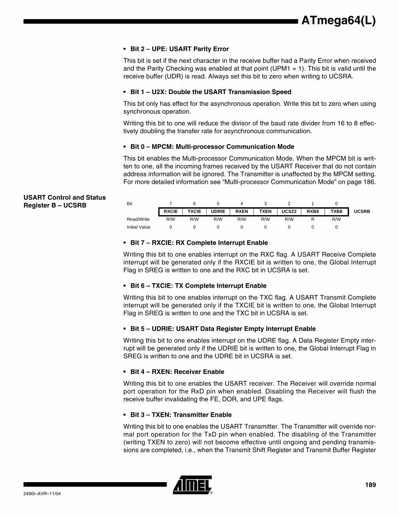
ATmega64(L)
• Bit 2 – UPE: USART Parity Error
This bit is set if the next character in the receive buffer had a Parity Error when receivedand the Parity Checking was enabled at that point (UPM1 = 1). This bit is valid until thereceive buffer (UDR) is read. Always set this bit to zero when writing to UCSRA.
• Bit 1 – U2X: Double the USART Transmission Speed
This bit only has effect for the asynchronous operation. Write this bit to zero when usingsynchronous operation.
Writing this bit to one will reduce the divisor of the baud rate divider from 16 to 8 effec-tively doubling the transfer rate for asynchronous communication.
• Bit 0 – MPCM: Multi-processor Communication Mode
This bit enables the Multi-processor Communication Mode. When the MPCM bit is writ-ten to one, all the incoming frames received by the USART Receiver that do not containaddress information will be ignored. The Transmitter is unaffected by the MPCM setting.For more detailed information see “Multi-processor Communication Mode” on page 186.
USART Control and Status Register B – UCSRB
• Bit 7 – RXCIE: RX Complete Interrupt Enable
Writing this bit to one enables interrupt on the RXC flag. A USART Receive Completeinterrupt will be generated only if the RXCIE bit is written to one, the Global InterruptFlag in SREG is written to one and the RXC bit in UCSRA is set.
• Bit 6 – TXCIE: TX Complete Interrupt Enable
Writing this bit to one enables interrupt on the TXC flag. A USART Transmit Completeinterrupt will be generated only if the TXCIE bit is written to one, the Global InterruptFlag in SREG is written to one and the TXC bit in UCSRA is set.
• Bit 5 – UDRIE: USART Data Register Empty Interrupt Enable
Writing this bit to one enables interrupt on the UDRE flag. A Data Register Empty inter-rupt will be generated only if the UDRIE bit is written to one, the Global Interrupt Flag inSREG is written to one and the UDRE bit in UCSRA is set.
• Bit 4 – RXEN: Receiver Enable
Writing this bit to one enables the USART receiver. The Receiver will override normalport operation for the RxD pin when enabled. Disabling the Receiver will flush thereceive buffer invalidating the FE, DOR, and UPE flags.
• Bit 3 – TXEN: Transmitter Enable
Writing this bit to one enables the USART Transmitter. The Transmitter will override nor-mal port operation for the TxD pin when enabled. The disabling of the Transmitter(writing TXEN to zero) will not become effective until ongoing and pending transmis-sions are completed, i.e., when the Transmit Shift Register and Transmit Buffer Register
Bit 7 6 5 4 3 2 1 0
RXCIE TXCIE UDRIE RXEN TXEN UCSZ2 RXB8 TXB8 UCSRBRead/Write R/W R/W R/W R/W R/W R/W R R/W
Initial Value 0 0 0 0 0 0 0 0
1892490I–AVR–11/04
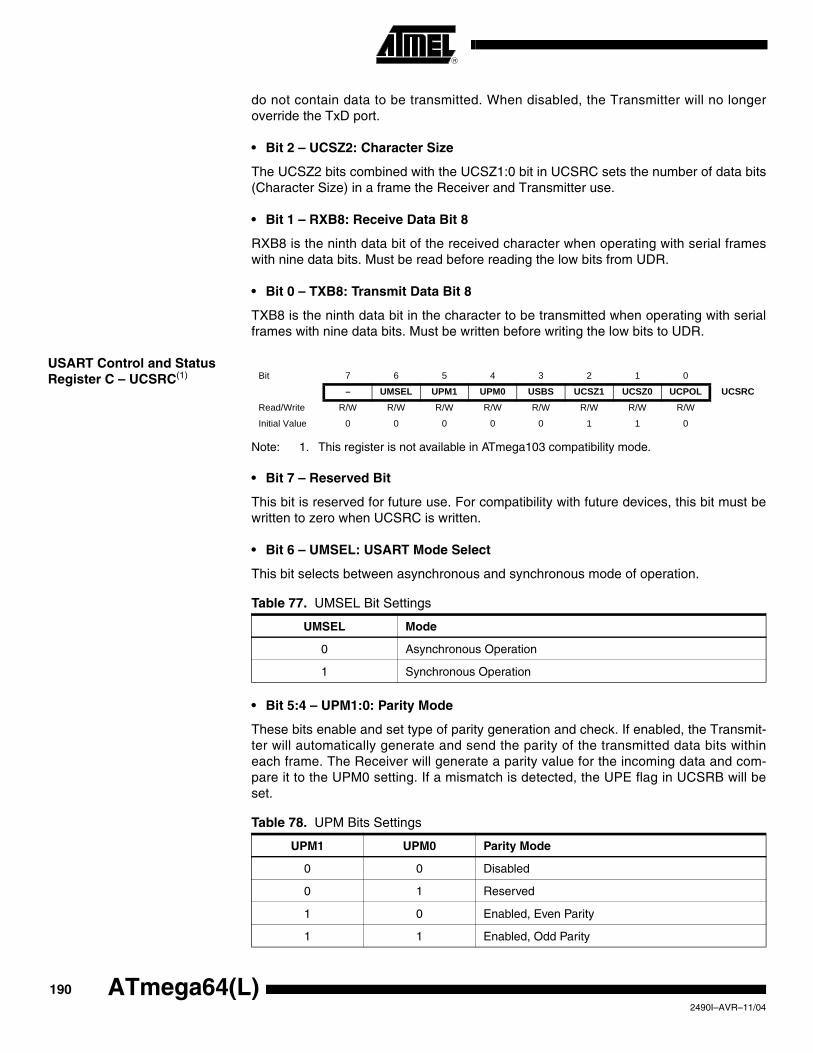
do not contain data to be transmitted. When disabled, the Transmitter will no longeroverride the TxD port.
• Bit 2 – UCSZ2: Character Size
The UCSZ2 bits combined with the UCSZ1:0 bit in UCSRC sets the number of data bits(Character Size) in a frame the Receiver and Transmitter use.
• Bit 1 – RXB8: Receive Data Bit 8
RXB8 is the ninth data bit of the received character when operating with serial frameswith nine data bits. Must be read before reading the low bits from UDR.
• Bit 0 – TXB8: Transmit Data Bit 8
TXB8 is the ninth data bit in the character to be transmitted when operating with serialframes with nine data bits. Must be written before writing the low bits to UDR.
USART Control and Status Register C – UCSRC(1)
Note: 1. This register is not available in ATmega103 compatibility mode.
• Bit 7 – Reserved Bit
This bit is reserved for future use. For compatibility with future devices, this bit must bewritten to zero when UCSRC is written.
• Bit 6 – UMSEL: USART Mode Select
This bit selects between asynchronous and synchronous mode of operation.
• Bit 5:4 – UPM1:0: Parity Mode
These bits enable and set type of parity generation and check. If enabled, the Transmit-ter will automatically generate and send the parity of the transmitted data bits withineach frame. The Receiver will generate a parity value for the incoming data and com-pare it to the UPM0 setting. If a mismatch is detected, the UPE flag in UCSRB will beset.
Bit 7 6 5 4 3 2 1 0
– UMSEL UPM1 UPM0 USBS UCSZ1 UCSZ0 UCPOL UCSRCRead/Write R/W R/W R/W R/W R/W R/W R/W R/W
Initial Value 0 0 0 0 0 1 1 0
Table 77. UMSEL Bit Settings
UMSEL Mode
0 Asynchronous Operation
1 Synchronous Operation
Table 78. UPM Bits Settings
UPM1 UPM0 Parity Mode
0 0 Disabled
0 1 Reserved
1 0 Enabled, Even Parity
1 1 Enabled, Odd Parity
190 ATmega64(L)2490I–AVR–11/04
ATmega64(L)
• Bit 3 – USBS: Stop Bit Select
This bit selects the number of stop bits to be inserted by the Transmitter. The Receiverignores this setting.
• Bit 2:1 – UCSZ1:0: Character Size
The UCSZ1:0 bits combined with the UCSZ2 bit in UCSRB sets the number of data bits(Character Size) in a frame the Receiver and Transmitter use.
• Bit 0 – UCPOL: Clock Polarity
This bit is used for synchronous mode only. Write this bit to zero when asynchronousmode is used. The UCPOL bit sets the relationship between data output change anddata input sample, and the synchronous clock (XCK).
Table 79. USBS Bit Settings
USBS Stop Bit(s)
0 1-bit
1 2-bit
Table 80. UCSZ Bits Settings
UCSZ2 UCSZ1 UCSZ0 Character Size
0 0 0 5-bit
0 0 1 6-bit
0 1 0 7-bit
0 1 1 8-bit
1 0 0 Reserved
1 0 1 Reserved
1 1 0 Reserved
1 1 1 9-bit
Table 81. UCPOL Bit Settings
UCPOLTransmitted Data Changed (Output of TxD Pin)
Received Data Sampled (Input on RxD Pin)
0 Rising XCK Edge Falling XCK Edge
1 Falling XCK Edge Rising XCK Edge
1912490I–AVR–11/04
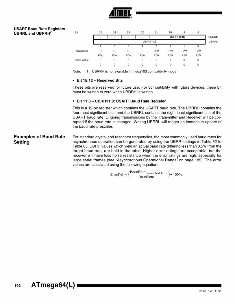
USART Baud Rate Registers – UBRRL and UBRRH(1)
Note: 1. UBRRH is not available in mega103 compatibility mode
• Bit 15:12 – Reserved Bits
These bits are reserved for future use. For compatibility with future devices, these bitmust be written to zero when UBRRH is written.
• Bit 11:0 – UBRR11:0: USART Baud Rate Register
This is a 12-bit register which contains the USART baud rate. The UBRRH contains thefour most significant bits, and the UBRRL contains the eight least significant bits of theUSART baud rate. Ongoing transmissions by the Transmitter and Receiver will be cor-rupted if the baud rate is changed. Writing UBRRL will trigger an immediate update ofthe baud rate prescaler.
Examples of Baud Rate Setting
For standard crystal and resonator frequencies, the most commonly used baud rates forasynchronous operation can be generated by using the UBRR settings in Table 82 toTable 85. UBRR values which yield an actual baud rate differing less than 0.5% from thetarget baud rate, are bold in the table. Higher error ratings are acceptable, but thereceiver will have less noise resistance when the error ratings are high, especially forlarge serial frames (see “Asynchronous Operational Range” on page 185). The errorvalues are calculated using the following equation:
Bit 15 14 13 12 11 10 9 8
– – – – UBRR[11:8] UBRRHUBRR[7:0] UBRRL
7 6 5 4 3 2 1 0
Read/Write R R R R R/W R/W R/W R/W
R/W R/W R/W R/W R/W R/W R/W R/W
Initial Value 0 0 0 0 0 0 0 0
0 0 0 0 0 0 0 0
Error[%]BaudRateClosest Match
BaudRate-------------------------------------------------------- 1–⎝ ⎠
⎛ ⎞ 100%•=
192 ATmega64(L)2490I–AVR–11/04
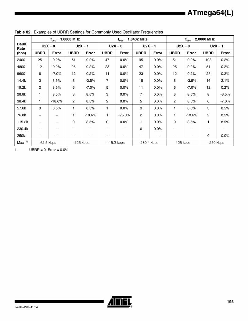
ATmega64(L)
Table 82. Examples of UBRR Settings for Commonly Used Oscillator Frequencies
Baud Rate (bps)
fosc = 1.0000 MHz fosc = 1.8432 MHz fosc = 2.0000 MHz
U2X = 0 U2X = 1 U2X = 0 U2X = 1 U2X = 0 U2X = 1
UBRR Error UBRR Error UBRR Error UBRR Error UBRR Error UBRR Error
2400 25 0.2% 51 0.2% 47 0.0% 95 0.0% 51 0.2% 103 0.2%
4800 12 0.2% 25 0.2% 23 0.0% 47 0.0% 25 0.2% 51 0.2%
9600 6 -7.0% 12 0.2% 11 0.0% 23 0.0% 12 0.2% 25 0.2%
14.4k 3 8.5% 8 -3.5% 7 0.0% 15 0.0% 8 -3.5% 16 2.1%
19.2k 2 8.5% 6 -7.0% 5 0.0% 11 0.0% 6 -7.0% 12 0.2%
28.8k 1 8.5% 3 8.5% 3 0.0% 7 0.0% 3 8.5% 8 -3.5%
38.4k 1 -18.6% 2 8.5% 2 0.0% 5 0.0% 2 8.5% 6 -7.0%
57.6k 0 8.5% 1 8.5% 1 0.0% 3 0.0% 1 8.5% 3 8.5%
76.8k – – 1 -18.6% 1 -25.0% 2 0.0% 1 -18.6% 2 8.5%
115.2k – – 0 8.5% 0 0.0% 1 0.0% 0 8.5% 1 8.5%
230.4k – – – – – – 0 0.0% – – – –
250k – – – – – – – – – – 0 0.0%
Max (1) 62.5 kbps 125 kbps 115.2 kbps 230.4 kbps 125 kbps 250 kbps
1. UBRR = 0, Error = 0.0%
1932490I–AVR–11/04
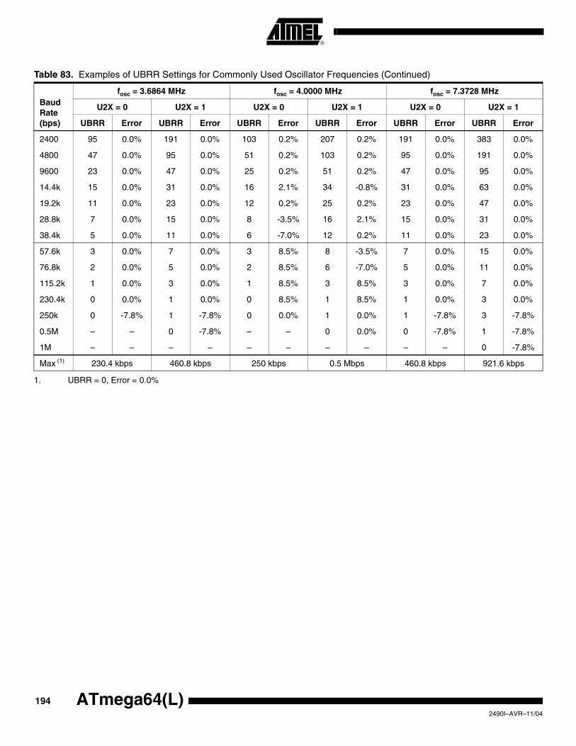
Table 83. Examples of UBRR Settings for Commonly Used Oscillator Frequencies (Continued)
Baud Rate (bps)
fosc = 3.6864 MHz fosc = 4.0000 MHz fosc = 7.3728 MHz
U2X = 0 U2X = 1 U2X = 0 U2X = 1 U2X = 0 U2X = 1
UBRR Error UBRR Error UBRR Error UBRR Error UBRR Error UBRR Error
2400 95 0.0% 191 0.0% 103 0.2% 207 0.2% 191 0.0% 383 0.0%
4800 47 0.0% 95 0.0% 51 0.2% 103 0.2% 95 0.0% 191 0.0%
9600 23 0.0% 47 0.0% 25 0.2% 51 0.2% 47 0.0% 95 0.0%
14.4k 15 0.0% 31 0.0% 16 2.1% 34 -0.8% 31 0.0% 63 0.0%
19.2k 11 0.0% 23 0.0% 12 0.2% 25 0.2% 23 0.0% 47 0.0%
28.8k 7 0.0% 15 0.0% 8 -3.5% 16 2.1% 15 0.0% 31 0.0%
38.4k 5 0.0% 11 0.0% 6 -7.0% 12 0.2% 11 0.0% 23 0.0%
57.6k 3 0.0% 7 0.0% 3 8.5% 8 -3.5% 7 0.0% 15 0.0%
76.8k 2 0.0% 5 0.0% 2 8.5% 6 -7.0% 5 0.0% 11 0.0%
115.2k 1 0.0% 3 0.0% 1 8.5% 3 8.5% 3 0.0% 7 0.0%
230.4k 0 0.0% 1 0.0% 0 8.5% 1 8.5% 1 0.0% 3 0.0%
250k 0 -7.8% 1 -7.8% 0 0.0% 1 0.0% 1 -7.8% 3 -7.8%
0.5M – – 0 -7.8% – – 0 0.0% 0 -7.8% 1 -7.8%
1M – – – – – – – – – – 0 -7.8%
Max (1) 230.4 kbps 460.8 kbps 250 kbps 0.5 Mbps 460.8 kbps 921.6 kbps
1. UBRR = 0, Error = 0.0%
194 ATmega64(L)2490I–AVR–11/04
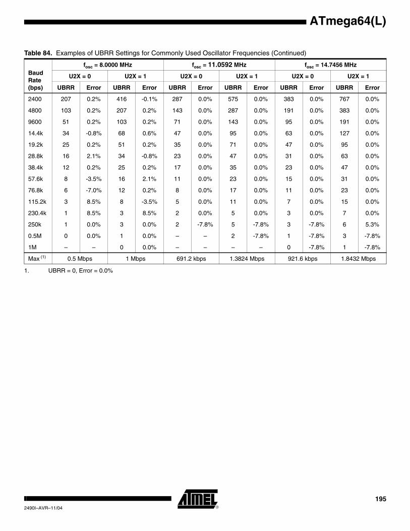
ATmega64(L)
Table 84. Examples of UBRR Settings for Commonly Used Oscillator Frequencies (Continued)
Baud Rate (bps)
fosc = 8.0000 MHz fosc = 11.0592 MHz fosc = 14.7456 MHz
U2X = 0 U2X = 1 U2X = 0 U2X = 1 U2X = 0 U2X = 1
UBRR Error UBRR Error UBRR Error UBRR Error UBRR Error UBRR Error
2400 207 0.2% 416 -0.1% 287 0.0% 575 0.0% 383 0.0% 767 0.0%
4800 103 0.2% 207 0.2% 143 0.0% 287 0.0% 191 0.0% 383 0.0%
9600 51 0.2% 103 0.2% 71 0.0% 143 0.0% 95 0.0% 191 0.0%
14.4k 34 -0.8% 68 0.6% 47 0.0% 95 0.0% 63 0.0% 127 0.0%
19.2k 25 0.2% 51 0.2% 35 0.0% 71 0.0% 47 0.0% 95 0.0%
28.8k 16 2.1% 34 -0.8% 23 0.0% 47 0.0% 31 0.0% 63 0.0%
38.4k 12 0.2% 25 0.2% 17 0.0% 35 0.0% 23 0.0% 47 0.0%
57.6k 8 -3.5% 16 2.1% 11 0.0% 23 0.0% 15 0.0% 31 0.0%
76.8k 6 -7.0% 12 0.2% 8 0.0% 17 0.0% 11 0.0% 23 0.0%
115.2k 3 8.5% 8 -3.5% 5 0.0% 11 0.0% 7 0.0% 15 0.0%
230.4k 1 8.5% 3 8.5% 2 0.0% 5 0.0% 3 0.0% 7 0.0%
250k 1 0.0% 3 0.0% 2 -7.8% 5 -7.8% 3 -7.8% 6 5.3%
0.5M 0 0.0% 1 0.0% – – 2 -7.8% 1 -7.8% 3 -7.8%
1M – – 0 0.0% – – – – 0 -7.8% 1 -7.8%
Max (1) 0.5 Mbps 1 Mbps 691.2 kbps 1.3824 Mbps 921.6 kbps 1.8432 Mbps
1. UBRR = 0, Error = 0.0%
1952490I–AVR–11/04
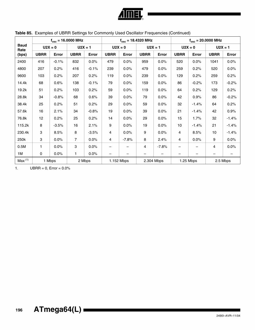
Table 85. Examples of UBRR Settings for Commonly Used Oscillator Frequencies (Continued)
Baud Rate (bps)
fosc = 16.0000 MHz fosc = 18.4320 MHz fosc = 20.0000 MHz
U2X = 0 U2X = 1 U2X = 0 U2X = 1 U2X = 0 U2X = 1
UBRR Error UBRR Error UBRR Error UBRR Error UBRR Error UBRR Error
2400 416 -0.1% 832 0.0% 479 0.0% 959 0.0% 520 0.0% 1041 0.0%
4800 207 0.2% 416 -0.1% 239 0.0% 479 0.0% 259 0.2% 520 0.0%
9600 103 0.2% 207 0.2% 119 0.0% 239 0.0% 129 0.2% 259 0.2%
14.4k 68 0.6% 138 -0.1% 79 0.0% 159 0.0% 86 -0.2% 173 -0.2%
19.2k 51 0.2% 103 0.2% 59 0.0% 119 0.0% 64 0.2% 129 0.2%
28.8k 34 -0.8% 68 0.6% 39 0.0% 79 0.0% 42 0.9% 86 -0.2%
38.4k 25 0.2% 51 0.2% 29 0.0% 59 0.0% 32 -1.4% 64 0.2%
57.6k 16 2.1% 34 -0.8% 19 0.0% 39 0.0% 21 -1.4% 42 0.9%
76.8k 12 0.2% 25 0.2% 14 0.0% 29 0.0% 15 1.7% 32 -1.4%
115.2k 8 -3.5% 16 2.1% 9 0.0% 19 0.0% 10 -1.4% 21 -1.4%
230.4k 3 8.5% 8 -3.5% 4 0.0% 9 0.0% 4 8.5% 10 -1.4%
250k 3 0.0% 7 0.0% 4 -7.8% 8 2.4% 4 0.0% 9 0.0%
0.5M 1 0.0% 3 0.0% – – 4 -7.8% – – 4 0.0%
1M 0 0.0% 1 0.0% – – – – – – – –
Max (1) 1 Mbps 2 Mbps 1.152 Mbps 2.304 Mbps 1.25 Mbps 2.5 Mbps
1. UBRR = 0, Error = 0.0%
196 ATmega64(L)2490I–AVR–11/04
ATmega64(L)
Two-wire Serial Interface
Features • Simple yet Powerful and Flexible Communication Interface, Only Two Bus Lines Needed• Both Master and Slave Operation Supported• Device can Operate as Transmitter or Receiver• 7-bit Address Space allows up to 128 Different Slave Addresses• Multi-master Arbitration Support• Up to 400 kHz Data Transfer Speed• Slew-rate Limited Output Drivers• Noise Suppression Circuitry Rejects Spikes on Bus Lines• Fully Programmable Slave Address with General Call Support• Address Recognition Causes Wake-up when AVR is in Sleep Mode
Two-wire Serial Interface Bus Definition
The Two-wire Serial Interface (TWI) is ideally suited for typical microcontroller applica-tions. The TWI protocol allows the systems designer to interconnect up to 128 differentdevices using only two bi-directional bus lines, one for clock (SCL) and one for data(SDA). The only external hardware needed to implement the bus is a single pull-upresistor for each of the TWI bus lines. All devices connected to the bus have individualaddresses, and mechanisms for resolving bus contention are inherent in the TWIprotocol.
Figure 86. TWI Bus Interconnection
TWI Terminology The following definitions are frequently encountered in this section.
Device 1 Device 2 Device 3 Device n
SDA
SCL
........ R1 R2
VCC
Table 86. TWI Terminology
Term Description
Master The device that initiates and terminates a transmission. The Master also generates the SCL clock.
Slave The device addressed by a Master.
Transmitter The device placing data on the bus.
Receiver The device reading data from the bus.
1972490I–AVR–11/04
Electrical Interconnection As depicted in Figure 86, both bus lines are connected to the positive supply voltagethrough pull-up resistors. The bus drivers of all TWI-compliant devices are open-drain oropen-collector. This implements a wired-AND function which is essential to the opera-tion of the interface. A low level on a TWI bus line is generated when one or more TWIdevices output a zero. A high level is output when all TWI devices tri-state their outputs,allowing the pull-up resistors to pull the line high. Note that all AVR devices connected tothe TWI bus must be powered in order to allow any bus operation.
The number of devices that can be connected to the bus is only limited by the buscapacitance limit of 400 pF and the 7-bit slave address space. A detailed specification ofthe electrical characteristics of the TWI is given in “Two-wire Serial Interface Character-istics” on page 330. Two different sets of specifications are presented there, onerelevant for bus speeds below 100 kHz, and one valid for bus speeds up to 400 kHz.
Data Transfer and Frame Format
Transferring Bits Each data bit transferred on the TWI bus is accompanied by a pulse on the clock line.The level of the data line must be stable when the clock line is high. The only exceptionto this rule is for generating start and stop conditions.
Figure 87. Data Validity
START and STOP Conditions The Master initiates and terminates a data transmission. The transmission is initiatedwhen the Master issues a START condition on the bus, and it is terminated when theMaster issues a STOP condition. Between a START and a STOP condition, the bus isconsidered busy, and no other Master should try to seize control of the bus. A specialcase occurs when a new START condition is issued between a START and STOP con-dition. This is referred to as a REPEATED START condition, and is used when theMaster wishes to initiate a new transfer without relinquishing control of the bus. After aREPEATED START, the bus is considered busy until the next STOP. This is identical tothe START behavior, and therefore START is used to describe both START andREPEATED START for the remainder of this data sheet, unless otherwise noted. Asdepicted below, START and STOP conditions are signalled by changing the level of theSDA line when the SCL line is high.
SDA
SCL
Data Stable Data Stable
Data Change
198 ATmega64(L)2490I–AVR–11/04
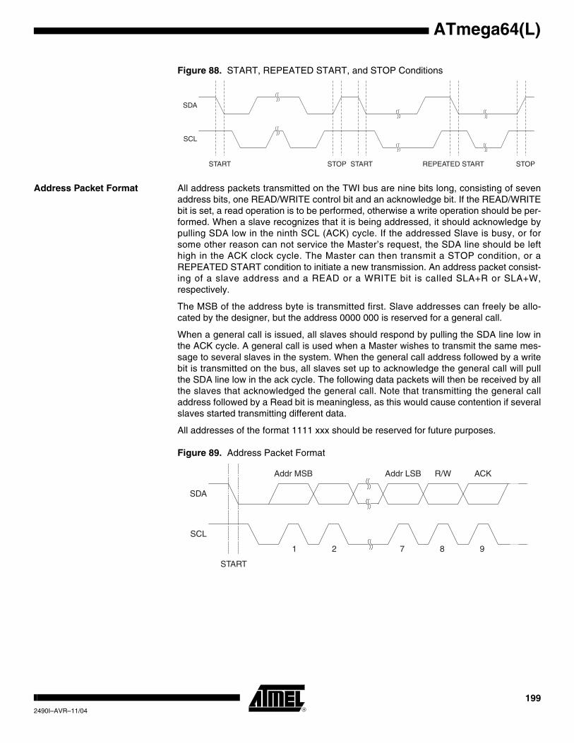
ATmega64(L)
Figure 88. START, REPEATED START, and STOP Conditions
Address Packet Format All address packets transmitted on the TWI bus are nine bits long, consisting of sevenaddress bits, one READ/WRITE control bit and an acknowledge bit. If the READ/WRITEbit is set, a read operation is to be performed, otherwise a write operation should be per-formed. When a slave recognizes that it is being addressed, it should acknowledge bypulling SDA low in the ninth SCL (ACK) cycle. If the addressed Slave is busy, or forsome other reason can not service the Master’s request, the SDA line should be lefthigh in the ACK clock cycle. The Master can then transmit a STOP condition, or aREPEATED START condition to initiate a new transmission. An address packet consist-ing of a slave address and a READ or a WRITE bit is called SLA+R or SLA+W,respectively.
The MSB of the address byte is transmitted first. Slave addresses can freely be allo-cated by the designer, but the address 0000 000 is reserved for a general call.
When a general call is issued, all slaves should respond by pulling the SDA line low inthe ACK cycle. A general call is used when a Master wishes to transmit the same mes-sage to several slaves in the system. When the general call address followed by a writebit is transmitted on the bus, all slaves set up to acknowledge the general call will pullthe SDA line low in the ack cycle. The following data packets will then be received by allthe slaves that acknowledged the general call. Note that transmitting the general calladdress followed by a Read bit is meaningless, as this would cause contention if severalslaves started transmitting different data.
All addresses of the format 1111 xxx should be reserved for future purposes.
Figure 89. Address Packet Format
SDA
SCL
START STOPREPEATED STARTSTOP START
SDA
SCL
START
1 2 7 8 9
Addr MSB Addr LSB R/W ACK
1992490I–AVR–11/04
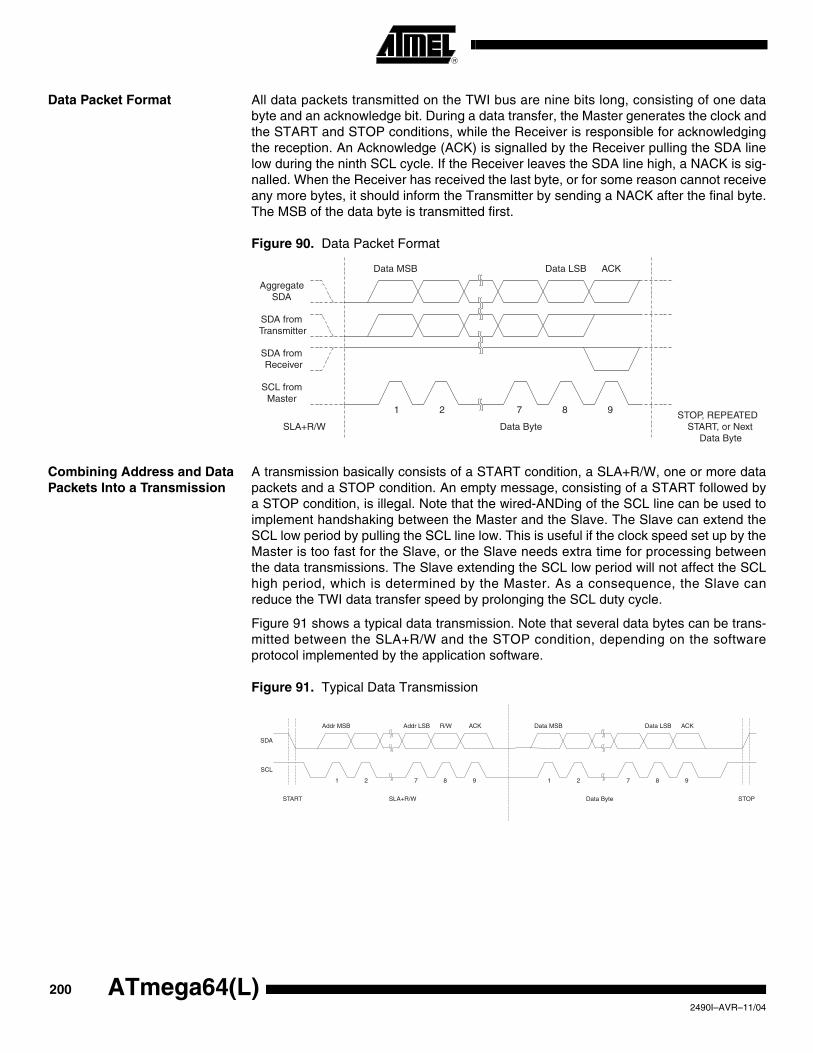
Data Packet Format All data packets transmitted on the TWI bus are nine bits long, consisting of one databyte and an acknowledge bit. During a data transfer, the Master generates the clock andthe START and STOP conditions, while the Receiver is responsible for acknowledgingthe reception. An Acknowledge (ACK) is signalled by the Receiver pulling the SDA linelow during the ninth SCL cycle. If the Receiver leaves the SDA line high, a NACK is sig-nalled. When the Receiver has received the last byte, or for some reason cannot receiveany more bytes, it should inform the Transmitter by sending a NACK after the final byte.The MSB of the data byte is transmitted first.
Figure 90. Data Packet Format
Combining Address and Data Packets Into a Transmission
A transmission basically consists of a START condition, a SLA+R/W, one or more datapackets and a STOP condition. An empty message, consisting of a START followed bya STOP condition, is illegal. Note that the wired-ANDing of the SCL line can be used toimplement handshaking between the Master and the Slave. The Slave can extend theSCL low period by pulling the SCL line low. This is useful if the clock speed set up by theMaster is too fast for the Slave, or the Slave needs extra time for processing betweenthe data transmissions. The Slave extending the SCL low period will not affect the SCLhigh period, which is determined by the Master. As a consequence, the Slave canreduce the TWI data transfer speed by prolonging the SCL duty cycle.
Figure 91 shows a typical data transmission. Note that several data bytes can be trans-mitted between the SLA+R/W and the STOP condition, depending on the softwareprotocol implemented by the application software.
Figure 91. Typical Data Transmission
1 2 7 8 9
Data MSB Data LSB ACK
AggregateSDA
SDA fromTransmitter
SDA fromReceiver
SCL fromMaster
SLA+R/W Data ByteSTOP, REPEATED
START, or NextData Byte
1 2 7 8 9
Data Byte
Data MSB Data LSB ACK
SDA
SCL
START
1 2 7 8 9
Addr MSB Addr LSB R/W ACK
SLA+R/W STOP
200 ATmega64(L)2490I–AVR–11/04
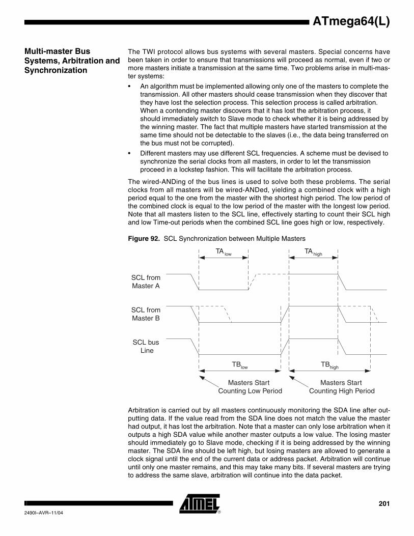
ATmega64(L)
Multi-master Bus Systems, Arbitration and Synchronization
The TWI protocol allows bus systems with several masters. Special concerns havebeen taken in order to ensure that transmissions will proceed as normal, even if two ormore masters initiate a transmission at the same time. Two problems arise in multi-mas-ter systems:
• An algorithm must be implemented allowing only one of the masters to complete the transmission. All other masters should cease transmission when they discover that they have lost the selection process. This selection process is called arbitration. When a contending master discovers that it has lost the arbitration process, it should immediately switch to Slave mode to check whether it is being addressed by the winning master. The fact that multiple masters have started transmission at the same time should not be detectable to the slaves (i.e., the data being transferred on the bus must not be corrupted).
• Different masters may use different SCL frequencies. A scheme must be devised to synchronize the serial clocks from all masters, in order to let the transmission proceed in a lockstep fashion. This will facilitate the arbitration process.
The wired-ANDing of the bus lines is used to solve both these problems. The serialclocks from all masters will be wired-ANDed, yielding a combined clock with a highperiod equal to the one from the master with the shortest high period. The low period ofthe combined clock is equal to the low period of the master with the longest low period.Note that all masters listen to the SCL line, effectively starting to count their SCL highand low Time-out periods when the combined SCL line goes high or low, respectively.
Figure 92. SCL Synchronization between Multiple Masters
Arbitration is carried out by all masters continuously monitoring the SDA line after out-putting data. If the value read from the SDA line does not match the value the masterhad output, it has lost the arbitration. Note that a master can only lose arbitration when itoutputs a high SDA value while another master outputs a low value. The losing mastershould immediately go to Slave mode, checking if it is being addressed by the winningmaster. The SDA line should be left high, but losing masters are allowed to generate aclock signal until the end of the current data or address packet. Arbitration will continueuntil only one master remains, and this may take many bits. If several masters are tryingto address the same slave, arbitration will continue into the data packet.
TA low TA high
SCL fromMaster A
SCL fromMaster B
SCL busLine
TBlow TBhigh
Masters StartCounting Low Period
Masters StartCounting High Period
2012490I–AVR–11/04
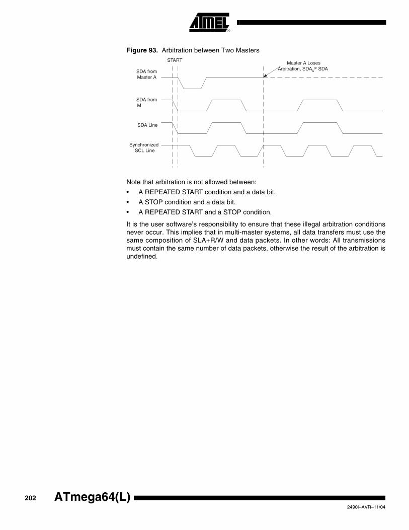
Figure 93. Arbitration between Two Masters
Note that arbitration is not allowed between:
• A REPEATED START condition and a data bit.
• A STOP condition and a data bit.
• A REPEATED START and a STOP condition.
It is the user software’s responsibility to ensure that these illegal arbitration conditionsnever occur. This implies that in multi-master systems, all data transfers must use thesame composition of SLA+R/W and data packets. In other words: All transmissionsmust contain the same number of data packets, otherwise the result of the arbitration isundefined.
SDA fromMaster A
SDA fromM
SDA Line
SynchronizedSCL Line
STARTMaster A Loses
Arbitration, SDAA SDA
202 ATmega64(L)2490I–AVR–11/04
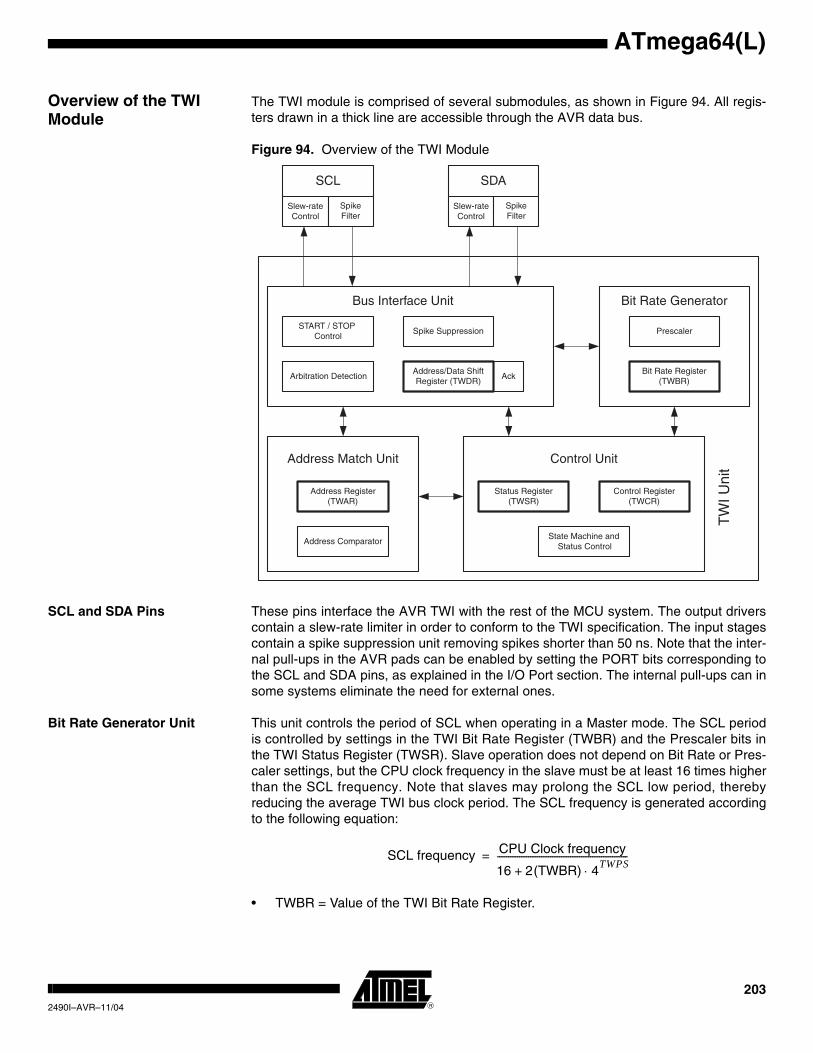
ATmega64(L)
Overview of the TWI Module
The TWI module is comprised of several submodules, as shown in Figure 94. All regis-ters drawn in a thick line are accessible through the AVR data bus.
Figure 94. Overview of the TWI Module
SCL and SDA Pins These pins interface the AVR TWI with the rest of the MCU system. The output driverscontain a slew-rate limiter in order to conform to the TWI specification. The input stagescontain a spike suppression unit removing spikes shorter than 50 ns. Note that the inter-nal pull-ups in the AVR pads can be enabled by setting the PORT bits corresponding tothe SCL and SDA pins, as explained in the I/O Port section. The internal pull-ups can insome systems eliminate the need for external ones.
Bit Rate Generator Unit This unit controls the period of SCL when operating in a Master mode. The SCL periodis controlled by settings in the TWI Bit Rate Register (TWBR) and the Prescaler bits inthe TWI Status Register (TWSR). Slave operation does not depend on Bit Rate or Pres-caler settings, but the CPU clock frequency in the slave must be at least 16 times higherthan the SCL frequency. Note that slaves may prolong the SCL low period, therebyreducing the average TWI bus clock period. The SCL frequency is generated accordingto the following equation:
• TWBR = Value of the TWI Bit Rate Register.
TW
I Uni
t
Address Register(TWAR)
Address Match Unit
Address Comparator
Control Unit
Control Register(TWCR)
Status Register(TWSR)
State Machine andStatus Control
SCL
Slew-rateControl
SpikeFilter
SDA
Slew-rateControl
SpikeFilter
Bit Rate Generator
Bit Rate Register(TWBR)
Prescaler
Bus Interface Unit
START / STOPControl
Arbitration Detection Ack
Spike Suppression
Address/Data ShiftRegister (TWDR)
SCL frequency CPU Clock frequency
16 2(TWBR) 4TWPS⋅+
-----------------------------------------------------------=
2032490I–AVR–11/04
• TWPS = Value of the prescaler bits in the TWI Status Register.Note: TWBR should be 10 or higher if the TWI operates in Master mode. If TWBR is lower than
10, the master may produce an incorrect output on SDA and SCL for the reminder of thebyte. The problem occurs when operating the TWI in Master mode, sending Start + SLA+ R/W to a slave (a slave does not need to be connected to the bus for the condition tohappen).
Bus Interface Unit This unit contains the Data and Address Shift Register (TWDR), a START/STOP Con-troller and Arbitration detection hardware. The TWDR contains the address or databytes to be transmitted, or the address or data bytes received. In addition to the 8-bitTWDR, the Bus Interface Unit also contains a register containing the (N)ACK bit to betransmitted or received. This (N)ACK Register is not directly accessible by the applica-tion software. However, when receiving, it can be set or cleared by manipulating theTWI Control Register (TWCR). When in Transmitter mode, the value of the received(N)ACK bit can be determined by the value in the TWSR.
The START/STOP Controller is responsible for generation and detection of START,REPEATED START, and STOP conditions. The START/STOP controller is able todetect START and STOP conditions even when the AVR MCU is in one of the sleepmodes, enabling the MCU to wake up if addressed by a Master.
If the TWI has initiated a transmission as Master, the Arbitration Detection hardwarecontinuously monitors the transmission trying to determine if arbitration is in process. Ifthe TWI has lost an arbitration, the Control Unit is informed. Correct action can then betaken and appropriate status codes generated.
Address Match Unit The Address Match unit checks if received address bytes match the 7-bit address in theTWI Address Register (TWAR). If the TWI General Call Recognition Enable (TWGCE)bit in the TWAR is written to one, all incoming address bits will also be comparedagainst the General Call address. Upon an address match, the Control unit is informed,allowing correct action to be taken. The TWI may or may not acknowledge its address,depending on settings in the TWCR. The Address Match unit is able to compareaddresses even when the AVR MCU is in sleep mode, enabling the MCU to wake-up ifaddressed by a Master.
Control Unit The Control unit monitors the TWI bus and generates responses corresponding to set-tings in the TWI Control Register (TWCR). When an event requiring the attention of theapplication occurs on the TWI bus, the TWI Interrupt Flag (TWINT) is asserted. In thenext clock cycle, the TWI Status Register (TWSR) is updated with a status code identify-ing the event. The TWSR only contains relevant status information when the TWIinterrupt flag is asserted. At all other times, the TWSR contains a special status codeindicating that no relevant status information is available. As long as the TWINT flag isset, the SCL line is held low. This allows the application software to complete its tasksbefore allowing the TWI transmission to continue.
The TWINT flag is set in the following situations:
• After the TWI has transmitted a START/REPEATED START condition.
• After the TWI has transmitted SLA+R/W.
• After the TWI has transmitted an address byte.
• After the TWI has lost arbitration.
• After the TWI has been addressed by own slave address or general call.
• After the TWI has received a data byte.
• After a STOP or REPEATED START has been received while still addressed as a Slave.
204 ATmega64(L)2490I–AVR–11/04

ATmega64(L)
• When a bus error has occurred due to an illegal START or STOP condition.
2052490I–AVR–11/04
TWI Register Description
TWI Bit Rate Register – TWBR
• Bits 7..0 – TWI Bit Rate Register
TWBR selects the division factor for the bit rate generator. The bit rate generator is afrequency divider which generates the SCL clock frequency in the Master modes. See“Bit Rate Generator Unit” on page 203 for calculating bit rates.
TWI Control Register – TWCR
The TWCR is used to control the operation of the TWI. It is used to enable the TWI, toinitiate a Master access by applying a START condition to the bus, to generate aReceiver acknowledge, to generate a stop condition, and to control halting of the buswhile the data to be written to the bus are written to the TWDR. It also indicates a writecollision if data is attempted written to TWDR while the register is inaccessible.
• Bit 7 – TWINT: TWI Interrupt Flag
This bit is set by hardware when the TWI has finished its current job and expects appli-cation software response. If the I-bit in SREG and TWIE in TWCR are set, the MCU willjump to the TWI Interrupt Vector. While the TWINT flag is set, the SCL low period isstretched. The TWINT flag must be cleared by software by writing a logic one to it. Notethat this flag is not automatically cleared by hardware when executing the interrupt rou-tine. Also note that clearing this flag starts the operation of the TWI, so all accesses tothe TWI Address Register (TWAR), TWI Status Register (TWSR), and TWI Data Regis-ter (TWDR) must be complete before clearing this flag.
• Bit 6 – TWEA: TWI Enable Acknowledge Bit
The TWEA bit controls the generation of the acknowledge pulse. If the TWEA bit is writ-ten to one, the ACK pulse is generated on the TWI bus if the following conditions aremet:
1. The device’s own slave address has been received.
2. A general call has been received, while the TWGCE bit in the TWAR is set.
3. A data byte has been received in Master Receiver or Slave Receiver mode.
By writing the TWEA bit to zero, the device can be virtually disconnected from the Two-wire Serial Bus temporarily. Address recognition can then be resumed by writing theTWEA bit to one again.
• Bit 5 – TWSTA: TWI START Condition Bit
The application writes the TWSTA bit to one when it desires to become a Master on theTwo-wire Serial Bus. The TWI hardware checks if the bus is available, and generates aSTART condition on the bus if it is free. However, if the bus is not free, the TWI waitsuntil a STOP condition is detected, and then generates a new START condition to claim
Bit 7 6 5 4 3 2 1 0
TWBR7 TWBR6 TWBR5 TWBR4 TWBR3 TWBR2 TWBR1 TWBR0 TWBRRead/Write R/W R/W R/W R/W R/W R/W R/W R/W
Initial Value 0 0 0 0 0 0 0 0
Bit 7 6 5 4 3 2 1 0
TWINT TWEA TWSTA TWSTO TWWC TWEN – TWIE TWCRRead/Write R/W R/W R/W R/W R R/W R R/W
Initial Value 0 0 0 0 0 0 0 0
206 ATmega64(L)2490I–AVR–11/04
ATmega64(L)
the Bus Master status. TWSTA must be cleared by software when the START conditionhas been transmitted.
• Bit 4 – TWSTO: TWI STOP Condition Bit
Writing the TWSTO bit to one in Master mode will generate a STOP condition on theTwo-wire Serial Bus. When the STOP condition is executed on the bus, the TWSTO bitis cleared automatically. In Slave mode, setting the TWSTO bit can be used to recoverfrom an error condition. This will not generate a STOP condition, but the TWI returns toa well-defined unaddressed Slave mode and releases the SCL and SDA lines to a highimpedance state.
• Bit 3 – TWWC: TWI Write Collision Flag
The TWWC bit is set when attempting to write to the TWI Data Register – TWDR whenTWINT is low. This flag is cleared by writing the TWDR Register when TWINT is high.
• Bit 2 – TWEN: TWI Enable Bit
The TWEN bit enables TWI operation and activates the TWI interface. When TWEN iswritten to one, the TWI takes control over the I/O pins connected to the SCL and SDApins, enabling the slew-rate limiters and spike filters. If this bit is written to zero, the TWIis switched off and all TWI transmissions are terminated, regardless of any ongoingoperation.
• Bit 1 – Res: Reserved Bit
This bit is a reserved bit and will always read as zero.
• Bit 0 – TWIE: TWI Interrupt Enable
When this bit is written to one, and the I-bit in SREG is set, the TWI interrupt request willbe activated for as long as the TWINT flag is high.
TWI Status Register – TWSR
• Bits 7..3 – TWS: TWI Status
These five bits reflect the status of the TWI logic and the Two-wire Serial Bus. The dif-ferent status codes are described later in this section. Note that the value read fromTWSR contains both the 5-bit status value and the 2-bit prescaler value. The applicationdesigner should mask the prescaler bits to zero when checking the status bits. Thismakes status checking independent of prescaler setting. This approach is used in thisdatasheet, unless otherwise noted.
• Bit 2 – Res: Reserved Bit
This bit is reserved and will always read as zero.
Bit 7 6 5 4 3 2 1 0
TWS7 TWS6 TWS5 TWS4 TWS3 – TWPS1 TWPS0 TWSRRead/Write R R R R R R R/W R/W
Initial Value 1 1 1 1 1 0 0 0
2072490I–AVR–11/04
• Bits 1..0 – TWPS: TWI Prescaler Bits
These bits can be read and written, and control the bit rate prescaler.
To calculate bit rates, see “Bit Rate Generator Unit” on page 203. The value ofTWPS1..0 is used in the equation.
TWI Data Register – TWDR
In Transmit mode, TWDR contains the next byte to be transmitted. In Receive mode, theTWDR contains the last byte received. It is writable while the TWI is not in the process ofshifting a byte. This occurs when the TWI Interrupt Flag (TWINT) is set by hardware.Note that the data register cannot be initialized by the user before the first interruptoccurs. The data in TWDR remains stable as long as TWINT is set. While data is shiftedout, data on the bus is simultaneously shifted in. TWDR always contains the last bytepresent on the bus, except after a wake-up from a sleep mode by the TWI interrupt. Inthis case, the contents of TWDR is undefined. In the case of a lost bus arbitration, nodata is lost in the transition from Master to Slave. Handling of the ACK bit is controlledautomatically by the TWI logic, the CPU cannot access the ACK bit directly.
• Bits 7..0 – TWD: TWI Data Register
These eight bits constitute the next data byte to be transmitted, or the latest data bytereceived on the Two-wire Serial Bus.
TWI (Slave) Address Register – TWAR
The TWAR should be loaded with the 7-bit slave address (in the seven most significantbits of TWAR) to which the TWI will respond when programmed as a slave transmitter orReceiver, and not needed in the Master modes. In multimaster systems, TWAR must beset in masters which can be addressed as slaves by other masters.
The LSB of TWAR is used to enable recognition of the general call address (0x00).There is an associated address comparator that looks for the slave address (or generalcall address if enabled) in the received serial address. If a match is found, an interruptrequest is generated.
• Bits 7..1 – TWA: TWI (Slave) Address Register
These seven bits constitute the slave address of the TWI unit.
Table 87. TWI Bit Rate Prescaler
TWPS1 TWPS0 Prescaler Value
0 0 1
0 1 4
1 0 16
1 1 64
Bit 7 6 5 4 3 2 1 0
TWD7 TWD6 TWD5 TWD4 TWD3 TWD2 TWD1 TWD0 TWDRRead/Write R/W R/W R/W R/W R/W R/W R/W R/W
Initial Value 1 1 1 1 1 1 1 1
Bit 7 6 5 4 3 2 1 0
TWA6 TWA5 TWA4 TWA3 TWA2 TWA1 TWA0 TWGCE TWARRead/Write R/W R/W R/W R/W R/W R/W R/W R/W
Initial Value 1 1 1 1 1 1 1 0
208 ATmega64(L)2490I–AVR–11/04
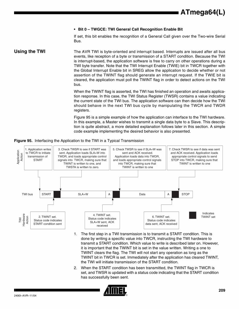
ATmega64(L)
• Bit 0 – TWGCE: TWI General Call Recognition Enable Bit
If set, this bit enables the recognition of a General Call given over the Two-wire SerialBus.
Using the TWI The AVR TWI is byte-oriented and interrupt based. Interrupts are issued after all busevents, like reception of a byte or transmission of a START condition. Because the TWIis interrupt-based, the application software is free to carry on other operations during aTWI byte transfer. Note that the TWI Interrupt Enable (TWIE) bit in TWCR together withthe Global Interrupt Enable bit in SREG allow the application to decide whether or notassertion of the TWINT flag should generate an interrupt request. If the TWIE bit iscleared, the application must poll the TWINT flag in order to detect actions on the TWIbus.
When the TWINT flag is asserted, the TWI has finished an operation and awaits applica-tion response. In this case, the TWI Status Register (TWSR) contains a value indicatingthe current state of the TWI bus. The application software can then decide how the TWIshould behave in the next TWI bus cycle by manipulating the TWCR and TWDRregisters.
Figure 95 is a simple example of how the application can interface to the TWI hardware.In this example, a Master wishes to transmit a single data byte to a Slave. This descrip-tion is quite abstract, a more detailed explanation follows later in this section. A simplecode example implementing the desired behavior is also presented.
Figure 95. Interfacing the Application to the TWI in a Typical Transmission
1. The first step in a TWI transmission is to transmit a START condition. This is done by writing a specific value into TWCR, instructing the TWI hardware to transmit a START condition. Which value to write is described later on. However, it is important that the TWINT bit is set in the value written. Writing a one to TWINT clears the flag. The TWI will not start any operation as long as the TWINT bit in TWCR is set. Immediately after the application has cleared TWINT, the TWI will initiate transmission of the START condition.
2. When the START condition has been transmitted, the TWINT flag in TWCR is set, and TWSR is updated with a status code indicating that the START condition has successfully been sent.
START SLA+W A Data A STOP
1. Application writesto TWCR to initiate
transmission of START
2. TWINT set.Status code indicatesSTART condition sent
4. TWINT set.Status code indicates
SLA+W sent, ACKreceived
6. TWINT set.Status code indicates
data sent, ACK received
3. Check TWSR to see if START was sent. Application loads SLA+W into
TWDR, and loads appropriate control signals into TWCR, making sure that
TWINT is written to one, and TWSTA is written to zero.
5. Check TWSR to see if SLA+W was sent and ACK received.
Application loads data into TWDR, and loads appropriate control signals
into TWCR, making sure that TWINT is written to one
7. Check TWSR to see if data was sent and ACK received. Application loads appropriate control signals to send STOP into TWCR, making sure that
TWINT is written to one
TWI bus
IndicatesTWINT set
App
licat
ion
Act
ion
TW
IH
ardw
are
Act
ion
2092490I–AVR–11/04
3. The application software should now examine the value of TWSR, to make sure that the START condition was successfully transmitted. If TWSR indicates other-wise, the application software might take some special action, like calling an error routine. Assuming that the status code is as expected, the application must load SLA+W into TWDR. Remember that TWDR is used both for address and data. After TWDR has been loaded with the desired SLA+W, a specific value must be written to TWCR, instructing the TWI hardware to transmit the SLA+W present in TWDR. Which value to write is described later on. However, it is important that the TWINT bit is set in the value written. Writing a one to TWINT clears the flag. The TWI will not start any operation as long as the TWINT bit in TWCR is set. Immediately after the application has cleared TWINT, the TWI will initiate transmission of the address packet.
4. When the address packet has been transmitted, the TWINT flag in TWCR is set, and TWSR is updated with a status code indicating that the address packet has successfully been sent. The status code will also reflect whether a slave acknowledged the packet or not.
5. The application software should now examine the value of TWSR, to make sure that the address packet was successfully transmitted, and that the value of the ACK bit was as expected. If TWSR indicates otherwise, the application software might take some special action, like calling an error routine. Assuming that the status code is as expected, the application must load a data packet into TWDR. Subsequently, a specific value must be written to TWCR, instructing the TWI hardware to transmit the data packet present in TWDR. Which value to write is described later on. However, it is important that the TWINT bit is set in the value written. Writing a one to TWINT clears the flag. The TWI will not start any opera-tion as long as the TWINT bit in TWCR is set. Immediately after the application has cleared TWINT, the TWI will initiate transmission of the data packet.
6. When the data packet has been transmitted, the TWINT flag in TWCR is set, and TWSR is updated with a status code indicating that the data packet has success-fully been sent. The status code will also reflect whether a slave acknowledged the packet or not.
7. The application software should now examine the value of TWSR, to make sure that the data packet was successfully transmitted, and that the value of the ACK bit was as expected. If TWSR indicates otherwise, the application software might take some special action, like calling an error routine. Assuming that the status code is as expected, the application must write a specific value to TWCR, instructing the TWI hardware to transmit a STOP condition. Which value to write is described later on. However, it is important that the TWINT bit is set in the value written. Writing a one to TWINT clears the flag. The TWI will not start any operation as long as the TWINT bit in TWCR is set. Immediately after the appli-cation has cleared TWINT, the TWI will initiate transmission of the STOP condition. Note that TWINT is NOT set after a STOP condition has been sent.
Even though this example is simple, it shows the principles involved in all TWI transmis-sions. These can be summarized as follows:
• When the TWI has finished an operation and expects application response, the TWINT flag is set. The SCL line is pulled low until TWINT is cleared.
• When the TWINT flag is set, the user must update all TWI registers with the value relevant for the next TWI bus cycle. As an example, TWDR must be loaded with the value to be transmitted in the next bus cycle.
• After all TWI Register updates and other pending application software tasks have been completed, TWCR is written. When writing TWCR, the TWINT bit should be
210 ATmega64(L)2490I–AVR–11/04

ATmega64(L)
set. Writing a one to TWINT clears the flag. The TWI will then commence executing whatever operation was specified by the TWCR setting.
In the following an assembly and C implementation of the example is given. Note thatthe code below assumes that several definitions have been made for example by usinginclude-files.
2112490I–AVR–11/04
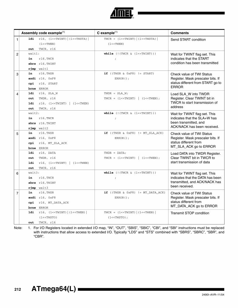
Note: 1. For I/O Registers located in extended I/O map, “IN”, “OUT”, “SBIS”, “SBIC”, “CBI”, and “SBI” instructions must be replacedwith instructions that allow access to extended I/O. Typically “LDS” and “STS” combined with “SBRS”, “SBRC”, “SBR”, and“CBR”.
Assembly code example(1) C example(1) Comments
1 ldi r16, (1<<TWINT)|(1<<TWSTA)|
(1<<TWEN)
out TWCR, r16
TWCR = (1<<TWINT)|(1<<TWSTA)|
(1<<TWEN)Send START condition
2 wait1:
in r16,TWCR
sbrs r16,TWINT
rjmp wait1
while (!(TWCR & (1<<TWINT)))
;Wait for TWINT flag set. This indicates that the START condition has been transmitted
3 in r16,TWSR
andi r16, 0xF8
cpi r16, START
brne ERROR
if ((TWSR & 0xF8) != START)
ERROR();Check value of TWI Status Register. Mask prescaler bits. If status different from START go to ERROR
4 ldi r16, SLA_W
out TWDR, r16
ldi r16, (1<<TWINT) | (1<<TWEN)
out TWCR, r16
TWDR = SLA_W;
TWCR = (1<<TWINT) | (1<<TWEN);Load SLA_W into TWDR Register. Clear TWINT bit in TWCR to start transmission of address
wait2:
in r16,TWCR
sbrs r16,TWINT
rjmp wait2
while (!(TWCR & (1<<TWINT)))
;Wait for TWINT flag set. This indicates that the SLA+W has been transmitted, and ACK/NACK has been received.
5 in r16,TWSR
andi r16, 0xF8
cpi r16, MT_SLA_ACK
brne ERROR
if ((TWSR & 0xF8) != MT_SLA_ACK)
ERROR();Check value of TWI Status Register. Mask prescaler bits. If status different from MT_SLA_ACK go to ERROR
ldi r16, DATA
out TWDR, r16
ldi r16, (1<<TWINT) | (1<<TWEN)
out TWCR, r16
TWDR = DATA;
TWCR = (1<<TWINT) | (1<<TWEN);Load DATA into TWDR Register. Clear TWINT bit in TWCR to start transmission of data
6 wait3:
in r16,TWCR
sbrs r16,TWINT
rjmp wait3
while (!(TWCR & (1<<TWINT)))
;Wait for TWINT flag set. This indicates that the DATA has been transmitted, and ACK/NACK has been received.
7 in r16,TWSR
andi r16, 0xF8
cpi r16, MT_DATA_ACK
brne ERROR
if ((TWSR & 0xF8) != MT_DATA_ACK)
ERROR();Check value of TWI Status Register. Mask prescaler bits. If status different from MT_DATA_ACK go to ERROR
ldi r16, (1<<TWINT)|(1<<TWEN)|
(1<<TWSTO)
out TWCR, r16
TWCR = (1<<TWINT)|(1<<TWEN)|
(1<<TWSTO);Transmit STOP condition
212 ATmega64(L)2490I–AVR–11/04
ATmega64(L)
Transmission Modes The TWI can operate in one of four major modes. These are named Master Transmitter(MT), Master Receiver (MR), Slave Transmitter (ST) and Slave Receiver (SR). Severalof these modes can be used in the same application. As an example, the TWI can useMT mode to write data into a TWI EEPROM, MR mode to read the data back from theEEPROM. If other masters are present in the system, some of these might transmit datato the TWI, and then SR mode would be used. It is the application software that decideswhich modes are legal.
The following sections describe each of these modes. Possible status codes aredescribed along with figures detailing data transmission in each of the modes. These fig-ures contain the following abbreviations:
S: START condition
Rs: REPEATED START condition
R: Read bit (high level at SDA)
W: Write bit (low level at SDA)
A: Acknowledge bit (low level at SDA)
A: Not acknowledge bit (high level at SDA)
Data: 8-bit data byte
P: STOP condition
SLA: Slave Address
In Figure 97 to Figure 103, circles are used to indicate that the TWINT flag is set. Thenumbers in the circles show the status code held in TWSR, with the prescaler bitsmasked to zero. At these points, actions must be taken by the application to continue orcomplete the TWI transfer. The TWI transfer is suspended until the TWINT flag iscleared by software.
When the TWINT flag is set, the status code in TWSR is used to determine the appropri-ate software action. For each status code, the required software action and details of thefollowing serial transfer are given in Table 88 to Table 91. Note that the prescaler bitsare masked to zero in these tables.
2132490I–AVR–11/04
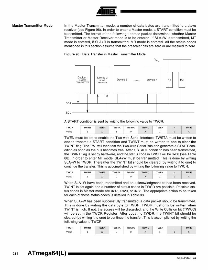
Master Transmitter Mode In the Master Transmitter mode, a number of data bytes are transmitted to a slavereceiver (see Figure 96). In order to enter a Master mode, a START condition must betransmitted. The format of the following address packet determines whether MasterTransmitter or Master Receiver mode is to be entered. If SLA+W is transmitted, MTmode is entered, if SLA+R is transmitted, MR mode is entered. All the status codesmentioned in this section assume that the prescaler bits are zero or are masked to zero.
Figure 96. Data Transfer in Master Transmitter Mode
A START condition is sent by writing the following value to TWCR:
TWEN must be set to enable the Two-wire Serial Interface, TWSTA must be written toone to transmit a START condition and TWINT must be written to one to clear theTWINT flag. The TWI will then test the Two-wire Serial Bus and generate a START con-dition as soon as the bus becomes free. After a START condition has been transmitted,the TWINT flag is set by hardware, and the status code in TWSR will be 0x08 (see Table88). In order to enter MT mode, SLA+W must be transmitted. This is done by writingSLA+W to TWDR. Thereafter the TWINT bit should be cleared (by writing it to one) tocontinue the transfer. This is accomplished by writing the following value to TWCR:
When SLA+W have been transmitted and an acknowledgment bit has been received,TWINT is set again and a number of status codes in TWSR are possible. Possible sta-tus codes in Master mode are 0x18, 0x20, or 0x38. The appropriate action to be takenfor each of these status codes is detailed in Table 88.
When SLA+W has been successfully transmitted, a data packet should be transmitted.This is done by writing the data byte to TWDR. TWDR must only be written whenTWINT is high. If not, the access will be discarded, and the Write Collision bit (TWWC)will be set in the TWCR Register. After updating TWDR, the TWINT bit should becleared (by writing it to one) to continue the transfer. This is accomplished by writing thefollowing value to TWCR:
TWCR TWINT TWEA TWSTA TWSTO TWWC TWEN – TWIEValue 1 X 1 0 X 1 0 X
TWCR TWINT TWEA TWSTA TWSTO TWWC TWEN – TWIEValue 1 X 0 0 X 1 0 X
TWCR TWINT TWEA TWSTA TWSTO TWWC TWEN – TWIEValue 1 X 0 0 X 1 0 X
Device 1MASTER
TRANSMITTER
Device 2SLAVE
RECEIVERDevice 3 Device n
SDA
SCL
........ R1 R2
VCC
214 ATmega64(L)2490I–AVR–11/04
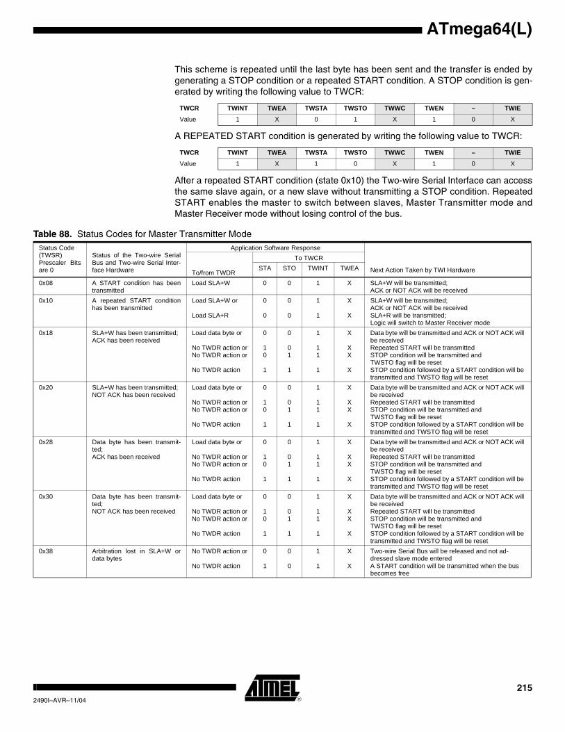
ATmega64(L)
This scheme is repeated until the last byte has been sent and the transfer is ended bygenerating a STOP condition or a repeated START condition. A STOP condition is gen-erated by writing the following value to TWCR:
A REPEATED START condition is generated by writing the following value to TWCR:
After a repeated START condition (state 0x10) the Two-wire Serial Interface can accessthe same slave again, or a new slave without transmitting a STOP condition. RepeatedSTART enables the master to switch between slaves, Master Transmitter mode andMaster Receiver mode without losing control of the bus.
TWCR TWINT TWEA TWSTA TWSTO TWWC TWEN – TWIEValue 1 X 0 1 X 1 0 X
TWCR TWINT TWEA TWSTA TWSTO TWWC TWEN – TWIEValue 1 X 1 0 X 1 0 X
Table 88. Status Codes for Master Transmitter ModeStatus Code(TWSR)Prescaler Bitsare 0
Status of the Two-wire SerialBus and Two-wire Serial Inter-face Hardware
Application Software Response
Next Action Taken by TWI HardwareTo/from TWDR
To TWCRSTA STO TWINT TWEA
0x08 A START condition has beentransmitted
Load SLA+W 0 0 1 X SLA+W will be transmitted;ACK or NOT ACK will be received
0x10 A repeated START conditionhas been transmitted
Load SLA+W or
Load SLA+R
0
0
0
0
1
1
X
X
SLA+W will be transmitted;ACK or NOT ACK will be receivedSLA+R will be transmitted;Logic will switch to Master Receiver mode
0x18 SLA+W has been transmitted;ACK has been received
Load data byte or
No TWDR action orNo TWDR action or
No TWDR action
0
10
1
0
01
1
1
11
1
X
XX
X
Data byte will be transmitted and ACK or NOT ACK will be receivedRepeated START will be transmittedSTOP condition will be transmitted andTWSTO flag will be resetSTOP condition followed by a START condition will be transmitted and TWSTO flag will be reset
0x20 SLA+W has been transmitted;NOT ACK has been received
Load data byte or
No TWDR action orNo TWDR action or
No TWDR action
0
10
1
0
01
1
1
11
1
X
XX
X
Data byte will be transmitted and ACK or NOT ACK will be receivedRepeated START will be transmittedSTOP condition will be transmitted andTWSTO flag will be resetSTOP condition followed by a START condition will be transmitted and TWSTO flag will be reset
0x28 Data byte has been transmit-ted;ACK has been received
Load data byte or
No TWDR action orNo TWDR action or
No TWDR action
0
10
1
0
01
1
1
11
1
X
XX
X
Data byte will be transmitted and ACK or NOT ACK will be receivedRepeated START will be transmittedSTOP condition will be transmitted andTWSTO flag will be resetSTOP condition followed by a START condition will be transmitted and TWSTO flag will be reset
0x30 Data byte has been transmit-ted;NOT ACK has been received
Load data byte or
No TWDR action orNo TWDR action or
No TWDR action
0
10
1
0
01
1
1
11
1
X
XX
X
Data byte will be transmitted and ACK or NOT ACK will be receivedRepeated START will be transmittedSTOP condition will be transmitted andTWSTO flag will be resetSTOP condition followed by a START condition will be transmitted and TWSTO flag will be reset
0x38 Arbitration lost in SLA+W ordata bytes
No TWDR action or
No TWDR action
0
1
0
0
1
1
X
X
Two-wire Serial Bus will be released and not ad-dressed slave mode enteredA START condition will be transmitted when the bus becomes free
2152490I–AVR–11/04
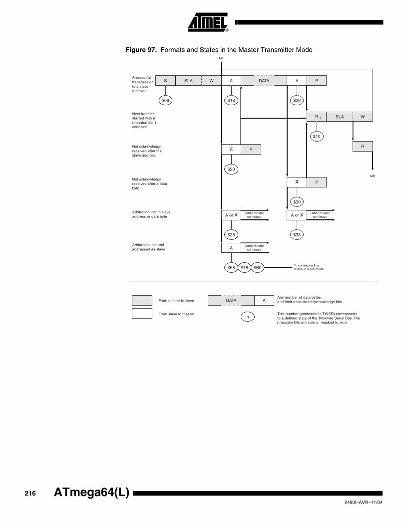
Figure 97. Formats and States in the Master Transmitter Mode
S SLA W A DATA A P
$08 $18 $28
R SLA W
$10
A P
$20
P
$30
A or A
$38
A
Other mastercontinues A or A
$38
Other mastercontinues
R
A
$68
Other mastercontinues
$78 $B0To correspondingstates in slave mode
MT
MR
Successfulltransmissionto a slavereceiver
Next transferstarted with arepeated startcondition
Not acknowledgereceived after theslave address
Not acknowledgereceived after a databyte
Arbitration lost in slaveaddress or data byte
Arbitration lost andaddressed as slave
DATA A
n
From master to slave
From slave to master
Any number of data bytesand their associated acknowledge bits
This number (contained in TWSR) correspondsto a defined state of the Two-wire Serial Bus. Theprescaler bits are zero or masked to zero
S
216 ATmega64(L)2490I–AVR–11/04
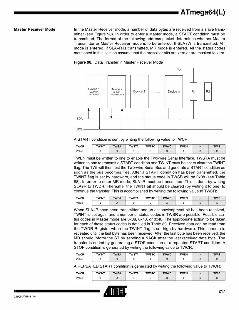
ATmega64(L)
Master Receiver Mode In the Master Receiver mode, a number of data bytes are received from a slave trans-mitter (see Figure 98). In order to enter a Master mode, a START condition must betransmitted. The format of the following address packet determines whether MasterTransmitter or Master Receiver mode is to be entered. If SLA+W is transmitted, MTmode is entered, if SLA+R is transmitted, MR mode is entered. All the status codesmentioned in this section assume that the prescaler bits are zero or are masked to zero.
Figure 98. Data Transfer in Master Receiver Mode
A START condition is sent by writing the following value to TWCR:
TWEN must be written to one to enable the Two-wire Serial Interface, TWSTA must bewritten to one to transmit a START condition and TWINT must be set to clear the TWINTflag. The TWI will then test the Two-wire Serial Bus and generate a START condition assoon as the bus becomes free. After a START condition has been transmitted, theTWINT flag is set by hardware, and the status code in TWSR will be 0x08 (see Table88). In order to enter MR mode, SLA+R must be transmitted. This is done by writingSLA+R to TWDR. Thereafter the TWINT bit should be cleared (by writing it to one) tocontinue the transfer. This is accomplished by writing the following value to TWCR:
When SLA+R have been transmitted and an acknowledgment bit has been received,TWINT is set again and a number of status codes in TWSR are possible. Possible sta-tus codes in Master mode are 0x38, 0x40, or 0x48. The appropriate action to be takenfor each of these status codes is detailed in Table 89. Received data can be read fromthe TWDR Register when the TWINT flag is set high by hardware. This scheme isrepeated until the last byte has been received. After the last byte has been received, theMR should inform the ST by sending a NACK after the last received data byte. Thetransfer is ended by generating a STOP condition or a repeated START condition. ASTOP condition is generated by writing the following value to TWCR:
A REPEATED START condition is generated by writing the following value to TWCR:
TWCR TWINT TWEA TWSTA TWSTO TWWC TWEN – TWIEValue 1 X 1 0 X 1 0 X
TWCR TWINT TWEA TWSTA TWSTO TWWC TWEN – TWIEValue 1 X 0 0 X 1 0 X
TWCR TWINT TWEA TWSTA TWSTO TWWC TWEN – TWIEValue 1 X 0 1 X 1 0 X
TWCR TWINT TWEA TWSTA TWSTO TWWC TWEN – TWIEValue 1 X 1 0 X 1 0 X
Device 1MASTER
RECEIVER
Device 2SLAVE
TRANSMITTERDevice 3 Device n
SDA
SCL
........ R1 R2
VCC
2172490I–AVR–11/04
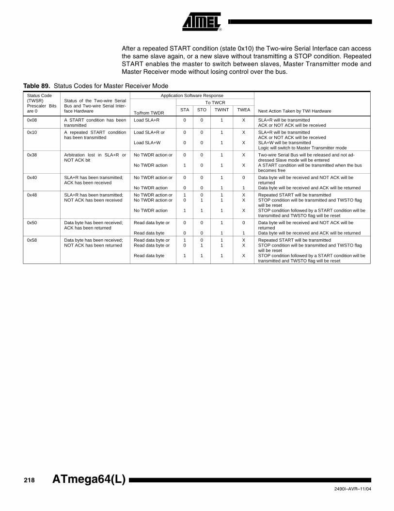
After a repeated START condition (state 0x10) the Two-wire Serial Interface can accessthe same slave again, or a new slave without transmitting a STOP condition. RepeatedSTART enables the master to switch between slaves, Master Transmitter mode andMaster Receiver mode without losing control over the bus.
Table 89. Status Codes for Master Receiver ModeStatus Code(TWSR)Prescaler Bitsare 0
Status of the Two-wire SerialBus and Two-wire Serial Inter-face Hardware
Application Software Response
Next Action Taken by TWI HardwareTo/from TWDR
To TWCRSTA STO TWINT TWEA
0x08 A START condition has beentransmitted
Load SLA+R 0 0 1 X SLA+R will be transmittedACK or NOT ACK will be received
0x10 A repeated START conditionhas been transmitted
Load SLA+R or
Load SLA+W
0
0
0
0
1
1
X
X
SLA+R will be transmittedACK or NOT ACK will be receivedSLA+W will be transmittedLogic will switch to Master Transmitter mode
0x38 Arbitration lost in SLA+R orNOT ACK bit
No TWDR action or
No TWDR action
0
1
0
0
1
1
X
X
Two-wire Serial Bus will be released and not ad-dressed Slave mode will be enteredA START condition will be transmitted when the busbecomes free
0x40 SLA+R has been transmitted;ACK has been received
No TWDR action or
No TWDR action
0
0
0
0
1
1
0
1
Data byte will be received and NOT ACK will be returnedData byte will be received and ACK will be returned
0x48 SLA+R has been transmitted;NOT ACK has been received
No TWDR action orNo TWDR action or
No TWDR action
10
1
01
1
11
1
XX
X
Repeated START will be transmittedSTOP condition will be transmitted and TWSTO flag will be resetSTOP condition followed by a START condition will be transmitted and TWSTO flag will be reset
0x50 Data byte has been received;ACK has been returned
Read data byte or
Read data byte
0
0
0
0
1
1
0
1
Data byte will be received and NOT ACK will be returnedData byte will be received and ACK will be returned
0x58 Data byte has been received;NOT ACK has been returned
Read data byte orRead data byte or
Read data byte
10
1
01
1
11
1
XX
X
Repeated START will be transmittedSTOP condition will be transmitted and TWSTO flag will be resetSTOP condition followed by a START condition will be transmitted and TWSTO flag will be reset
218 ATmega64(L)2490I–AVR–11/04
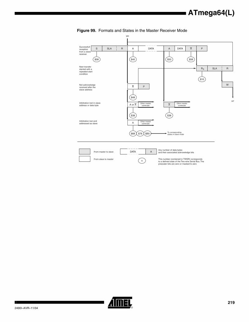
ATmega64(L)
Figure 99. Formats and States in the Master Receiver Mode
S SLA R A DATA A
$08 $40 $50
SLA R
$10
A P
$48
A or A
$38
Other mastercontinues
$38
Other mastercontinues
W
A
$68
Other mastercontinues
$78 $B0To correspondingstates in slave mode
MR
MT
Successfullreceptionfrom a slavereceiver
Next transferstarted with arepeated startcondition
Not acknowledgereceived after theslave address
Arbitration lost in slaveaddress or data byte
Arbitration lost andaddressed as slave
DATA A
n
From master to slave
From slave to master
Any number of data bytesand their associated acknowledge bits
This number (contained in TWSR) correspondsto a defined state of the Two-wire Serial Bus. The prescaler bits are zero or masked to zero
PDATA A
$58
A
RS
2192490I–AVR–11/04
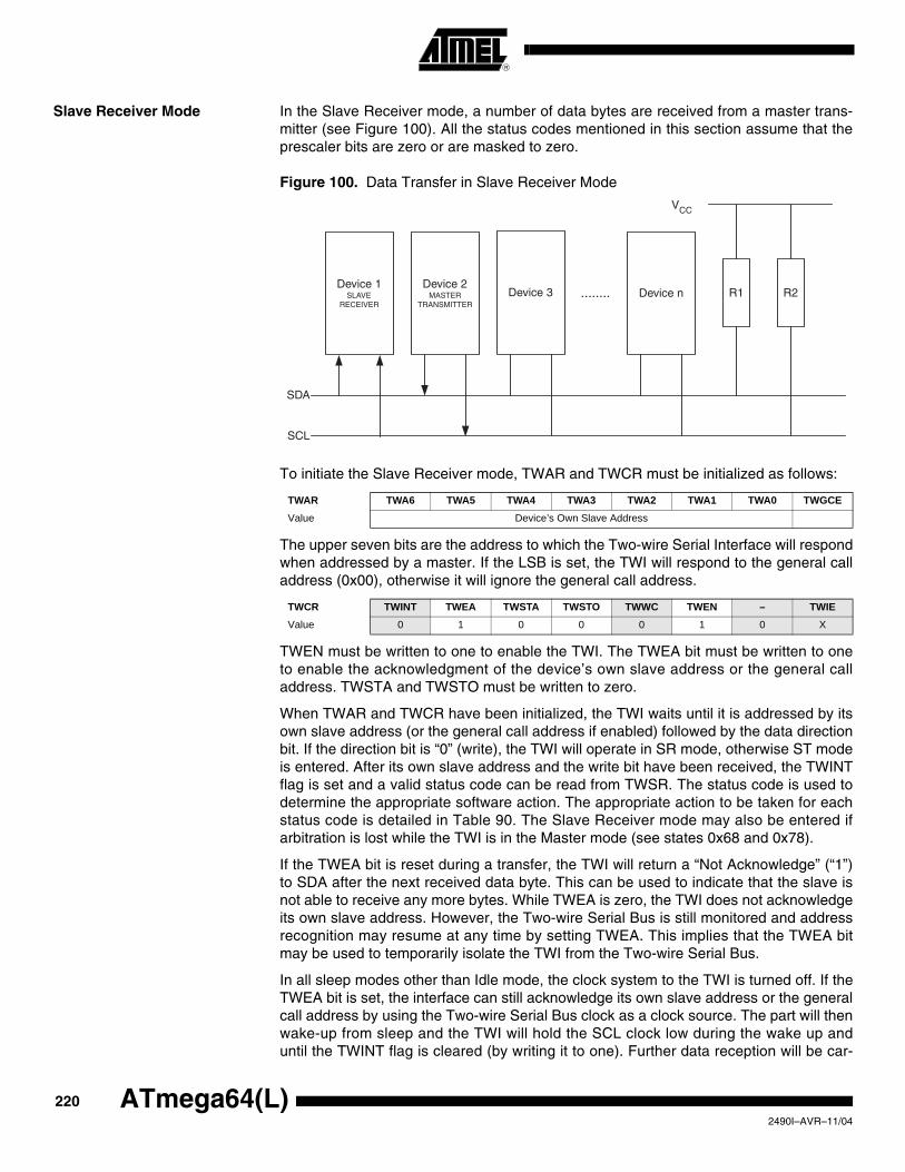
Slave Receiver Mode In the Slave Receiver mode, a number of data bytes are received from a master trans-mitter (see Figure 100). All the status codes mentioned in this section assume that theprescaler bits are zero or are masked to zero.
Figure 100. Data Transfer in Slave Receiver Mode
To initiate the Slave Receiver mode, TWAR and TWCR must be initialized as follows:
The upper seven bits are the address to which the Two-wire Serial Interface will respondwhen addressed by a master. If the LSB is set, the TWI will respond to the general calladdress (0x00), otherwise it will ignore the general call address.
TWEN must be written to one to enable the TWI. The TWEA bit must be written to oneto enable the acknowledgment of the device’s own slave address or the general calladdress. TWSTA and TWSTO must be written to zero.
When TWAR and TWCR have been initialized, the TWI waits until it is addressed by itsown slave address (or the general call address if enabled) followed by the data directionbit. If the direction bit is “0” (write), the TWI will operate in SR mode, otherwise ST modeis entered. After its own slave address and the write bit have been received, the TWINTflag is set and a valid status code can be read from TWSR. The status code is used todetermine the appropriate software action. The appropriate action to be taken for eachstatus code is detailed in Table 90. The Slave Receiver mode may also be entered ifarbitration is lost while the TWI is in the Master mode (see states 0x68 and 0x78).
If the TWEA bit is reset during a transfer, the TWI will return a “Not Acknowledge” (“1”)to SDA after the next received data byte. This can be used to indicate that the slave isnot able to receive any more bytes. While TWEA is zero, the TWI does not acknowledgeits own slave address. However, the Two-wire Serial Bus is still monitored and addressrecognition may resume at any time by setting TWEA. This implies that the TWEA bitmay be used to temporarily isolate the TWI from the Two-wire Serial Bus.
In all sleep modes other than Idle mode, the clock system to the TWI is turned off. If theTWEA bit is set, the interface can still acknowledge its own slave address or the generalcall address by using the Two-wire Serial Bus clock as a clock source. The part will thenwake-up from sleep and the TWI will hold the SCL clock low during the wake up anduntil the TWINT flag is cleared (by writing it to one). Further data reception will be car-
TWAR TWA6 TWA5 TWA4 TWA3 TWA2 TWA1 TWA0 TWGCEValue Device’s Own Slave Address
TWCR TWINT TWEA TWSTA TWSTO TWWC TWEN – TWIEValue 0 1 0 0 0 1 0 X
Device 3 Device n
SDA
SCL
........ R1 R2
VCC
Device 2MASTER
TRANSMITTER
Device 1SLAVE
RECEIVER
220 ATmega64(L)2490I–AVR–11/04
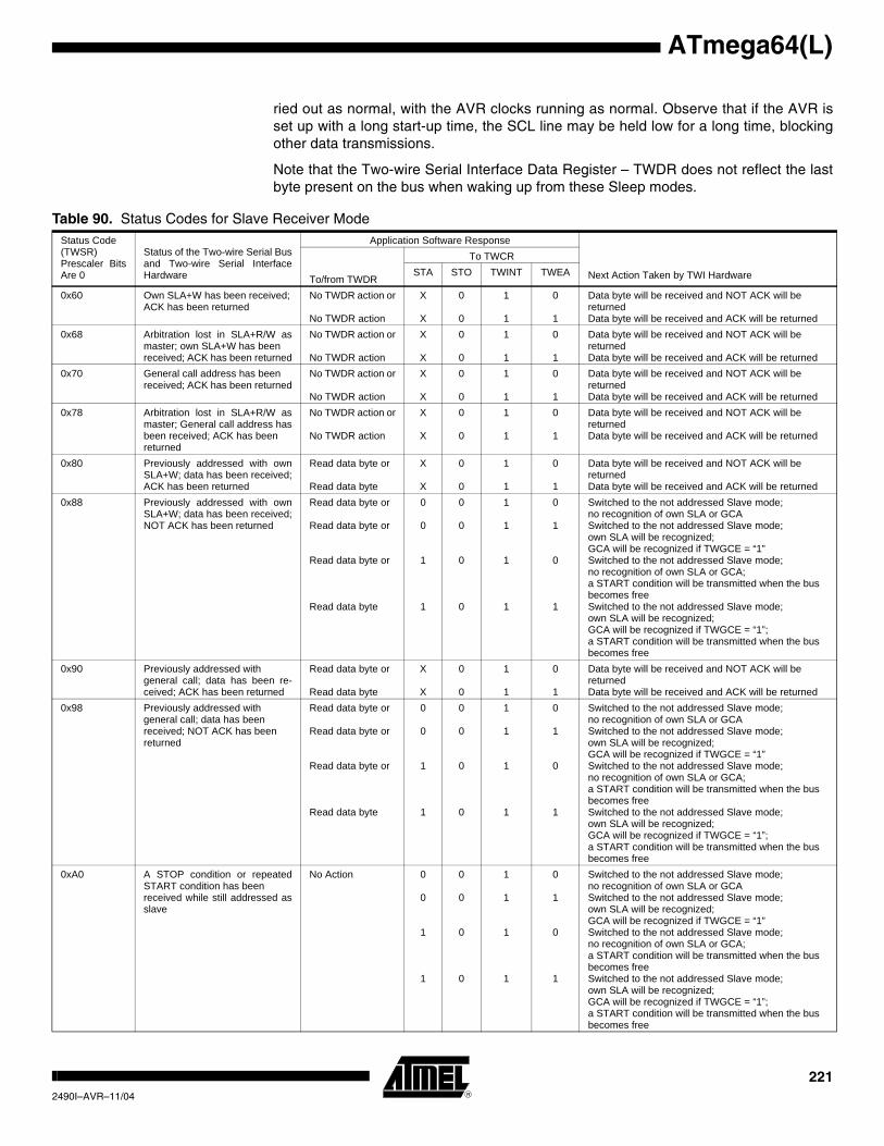
ATmega64(L)
ried out as normal, with the AVR clocks running as normal. Observe that if the AVR isset up with a long start-up time, the SCL line may be held low for a long time, blockingother data transmissions.
Note that the Two-wire Serial Interface Data Register – TWDR does not reflect the lastbyte present on the bus when waking up from these Sleep modes.
Table 90. Status Codes for Slave Receiver Mode Status Code(TWSR)Prescaler BitsAre 0
Status of the Two-wire Serial Busand Two-wire Serial InterfaceHardware
Application Software Response
Next Action Taken by TWI HardwareTo/from TWDR
To TWCRSTA STO TWINT TWEA
0x60 Own SLA+W has been received;ACK has been returned
No TWDR action or
No TWDR action
X
X
0
0
1
1
0
1
Data byte will be received and NOT ACK will be returnedData byte will be received and ACK will be returned
0x68 Arbitration lost in SLA+R/W asmaster; own SLA+W has been received; ACK has been returned
No TWDR action or
No TWDR action
X
X
0
0
1
1
0
1
Data byte will be received and NOT ACK will be returnedData byte will be received and ACK will be returned
0x70 General call address has been received; ACK has been returned
No TWDR action or
No TWDR action
X
X
0
0
1
1
0
1
Data byte will be received and NOT ACK will be returnedData byte will be received and ACK will be returned
0x78 Arbitration lost in SLA+R/W asmaster; General call address hasbeen received; ACK has been returned
No TWDR action or
No TWDR action
X
X
0
0
1
1
0
1
Data byte will be received and NOT ACK will be returnedData byte will be received and ACK will be returned
0x80 Previously addressed with ownSLA+W; data has been received;ACK has been returned
Read data byte or
Read data byte
X
X
0
0
1
1
0
1
Data byte will be received and NOT ACK will be returnedData byte will be received and ACK will be returned
0x88 Previously addressed with ownSLA+W; data has been received;NOT ACK has been returned
Read data byte or
Read data byte or
Read data byte or
Read data byte
0
0
1
1
0
0
0
0
1
1
1
1
0
1
0
1
Switched to the not addressed Slave mode;no recognition of own SLA or GCASwitched to the not addressed Slave mode;own SLA will be recognized;GCA will be recognized if TWGCE = “1”Switched to the not addressed Slave mode;no recognition of own SLA or GCA;a START condition will be transmitted when the bus becomes freeSwitched to the not addressed Slave mode;own SLA will be recognized;GCA will be recognized if TWGCE = “1”;a START condition will be transmitted when the bus becomes free
0x90 Previously addressed with general call; data has been re-ceived; ACK has been returned
Read data byte or
Read data byte
X
X
0
0
1
1
0
1
Data byte will be received and NOT ACK will be returnedData byte will be received and ACK will be returned
0x98 Previously addressed with general call; data has been received; NOT ACK has been returned
Read data byte or
Read data byte or
Read data byte or
Read data byte
0
0
1
1
0
0
0
0
1
1
1
1
0
1
0
1
Switched to the not addressed Slave mode;no recognition of own SLA or GCASwitched to the not addressed Slave mode;own SLA will be recognized;GCA will be recognized if TWGCE = “1”Switched to the not addressed Slave mode;no recognition of own SLA or GCA;a START condition will be transmitted when the bus becomes freeSwitched to the not addressed Slave mode;own SLA will be recognized;GCA will be recognized if TWGCE = “1”;a START condition will be transmitted when the bus becomes free
0xA0 A STOP condition or repeatedSTART condition has been received while still addressed asslave
No Action 0
0
1
1
0
0
0
0
1
1
1
1
0
1
0
1
Switched to the not addressed Slave mode;no recognition of own SLA or GCASwitched to the not addressed Slave mode;own SLA will be recognized;GCA will be recognized if TWGCE = “1”Switched to the not addressed Slave mode;no recognition of own SLA or GCA;a START condition will be transmitted when the bus becomes freeSwitched to the not addressed Slave mode;own SLA will be recognized;GCA will be recognized if TWGCE = “1”;a START condition will be transmitted when the bus becomes free
2212490I–AVR–11/04
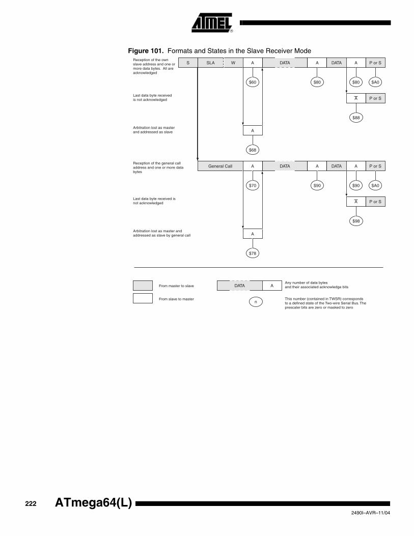
Figure 101. Formats and States in the Slave Receiver Mode
S SLA W A DATA A
$60 $80
$88
A
$68
Reception of the ownslave address and one ormore data bytes. All areacknowledged
Last data byte receivedis not acknowledged
Arbitration lost as masterand addressed as slave
Reception of the general calladdress and one or more databytes
Last data byte received isnot acknowledged
n
From master to slave
From slave to master
Any number of data bytesand their associated acknowledge bits
This number (contained in TWSR) correspondsto a defined state of the Two-wire Serial Bus. The prescaler bits are zero or masked to zero
P or SDATA A
$80 $A0
P or SA
A DATA A
$70 $90
$98
A
$78
P or SDATA A
$90 $A0
P or SA
General Call
Arbitration lost as master andaddressed as slave by general call
DATA A
222 ATmega64(L)2490I–AVR–11/04
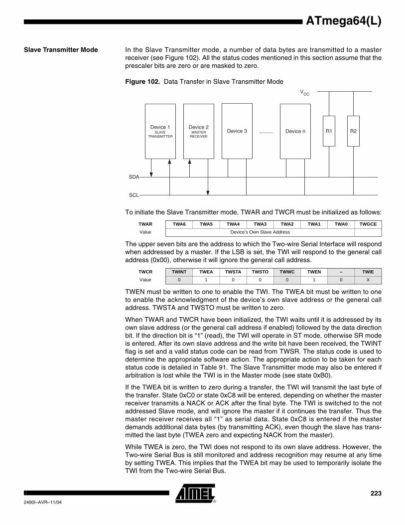
ATmega64(L)
Slave Transmitter Mode In the Slave Transmitter mode, a number of data bytes are transmitted to a masterreceiver (see Figure 102). All the status codes mentioned in this section assume that theprescaler bits are zero or are masked to zero.
Figure 102. Data Transfer in Slave Transmitter Mode
To initiate the Slave Transmitter mode, TWAR and TWCR must be initialized as follows:
The upper seven bits are the address to which the Two-wire Serial Interface will respondwhen addressed by a master. If the LSB is set, the TWI will respond to the general calladdress (0x00), otherwise it will ignore the general call address.
TWEN must be written to one to enable the TWI. The TWEA bit must be written to oneto enable the acknowledgment of the device’s own slave address or the general calladdress. TWSTA and TWSTO must be written to zero.
When TWAR and TWCR have been initialized, the TWI waits until it is addressed by itsown slave address (or the general call address if enabled) followed by the data directionbit. If the direction bit is “1” (read), the TWI will operate in ST mode, otherwise SR modeis entered. After its own slave address and the write bit have been received, the TWINTflag is set and a valid status code can be read from TWSR. The status code is used todetermine the appropriate software action. The appropriate action to be taken for eachstatus code is detailed in Table 91. The Slave Transmitter mode may also be entered ifarbitration is lost while the TWI is in the Master mode (see state 0xB0).
If the TWEA bit is written to zero during a transfer, the TWI will transmit the last byte ofthe transfer. State 0xC0 or state 0xC8 will be entered, depending on whether the masterreceiver transmits a NACK or ACK after the final byte. The TWI is switched to the notaddressed Slave mode, and will ignore the master if it continues the transfer. Thus themaster receiver receives all “1” as serial data. State 0xC8 is entered if the masterdemands additional data bytes (by transmitting ACK), even though the slave has trans-mitted the last byte (TWEA zero and expecting NACK from the master).
While TWEA is zero, the TWI does not respond to its own slave address. However, theTwo-wire Serial Bus is still monitored and address recognition may resume at any timeby setting TWEA. This implies that the TWEA bit may be used to temporarily isolate theTWI from the Two-wire Serial Bus.
TWAR TWA6 TWA5 TWA4 TWA3 TWA2 TWA1 TWA0 TWGCEValue Device’s Own Slave Address
TWCR TWINT TWEA TWSTA TWSTO TWWC TWEN – TWIEValue 0 1 0 0 0 1 0 X
Device 3 Device n
SDA
SCL
........ R1 R2
VCC
Device 2MASTER
RECEIVER
Device 1SLAVE
TRANSMITTER
2232490I–AVR–11/04
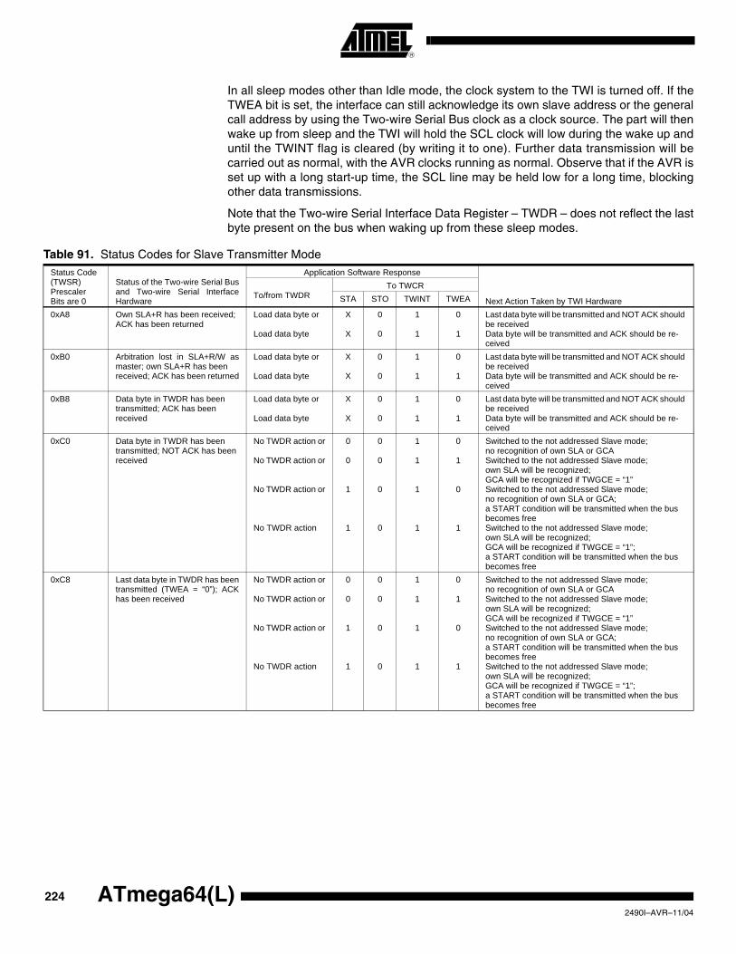
In all sleep modes other than Idle mode, the clock system to the TWI is turned off. If theTWEA bit is set, the interface can still acknowledge its own slave address or the generalcall address by using the Two-wire Serial Bus clock as a clock source. The part will thenwake up from sleep and the TWI will hold the SCL clock will low during the wake up anduntil the TWINT flag is cleared (by writing it to one). Further data transmission will becarried out as normal, with the AVR clocks running as normal. Observe that if the AVR isset up with a long start-up time, the SCL line may be held low for a long time, blockingother data transmissions.
Note that the Two-wire Serial Interface Data Register – TWDR – does not reflect the lastbyte present on the bus when waking up from these sleep modes.
Table 91. Status Codes for Slave Transmitter ModeStatus Code(TWSR)PrescalerBits are 0
Status of the Two-wire Serial Busand Two-wire Serial InterfaceHardware
Application Software Response
Next Action Taken by TWI HardwareTo/from TWDR
To TWCRSTA STO TWINT TWEA
0xA8 Own SLA+R has been received;ACK has been returned
Load data byte or
Load data byte
X
X
0
0
1
1
0
1
Last data byte will be transmitted and NOT ACK should be receivedData byte will be transmitted and ACK should be re-ceived
0xB0 Arbitration lost in SLA+R/W asmaster; own SLA+R has been received; ACK has been returned
Load data byte or
Load data byte
X
X
0
0
1
1
0
1
Last data byte will be transmitted and NOT ACK should be receivedData byte will be transmitted and ACK should be re-ceived
0xB8 Data byte in TWDR has been transmitted; ACK has been received
Load data byte or
Load data byte
X
X
0
0
1
1
0
1
Last data byte will be transmitted and NOT ACK should be receivedData byte will be transmitted and ACK should be re-ceived
0xC0 Data byte in TWDR has been transmitted; NOT ACK has been received
No TWDR action or
No TWDR action or
No TWDR action or
No TWDR action
0
0
1
1
0
0
0
0
1
1
1
1
0
1
0
1
Switched to the not addressed Slave mode;no recognition of own SLA or GCASwitched to the not addressed Slave mode;own SLA will be recognized;GCA will be recognized if TWGCE = “1”Switched to the not addressed Slave mode;no recognition of own SLA or GCA;a START condition will be transmitted when the bus becomes freeSwitched to the not addressed Slave mode;own SLA will be recognized;GCA will be recognized if TWGCE = “1”;a START condition will be transmitted when the bus becomes free
0xC8 Last data byte in TWDR has beentransmitted (TWEA = “0”); ACKhas been received
No TWDR action or
No TWDR action or
No TWDR action or
No TWDR action
0
0
1
1
0
0
0
0
1
1
1
1
0
1
0
1
Switched to the not addressed Slave mode;no recognition of own SLA or GCASwitched to the not addressed Slave mode;own SLA will be recognized;GCA will be recognized if TWGCE = “1”Switched to the not addressed Slave mode;no recognition of own SLA or GCA;a START condition will be transmitted when the bus becomes freeSwitched to the not addressed Slave mode;own SLA will be recognized;GCA will be recognized if TWGCE = “1”;a START condition will be transmitted when the bus becomes free
224 ATmega64(L)2490I–AVR–11/04
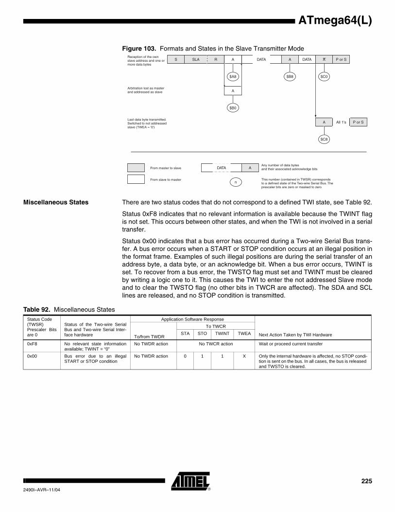
ATmega64(L)
Figure 103. Formats and States in the Slave Transmitter Mode
Miscellaneous States There are two status codes that do not correspond to a defined TWI state, see Table 92.
Status 0xF8 indicates that no relevant information is available because the TWINT flagis not set. This occurs between other states, and when the TWI is not involved in a serialtransfer.
Status 0x00 indicates that a bus error has occurred during a Two-wire Serial Bus trans-fer. A bus error occurs when a START or STOP condition occurs at an illegal position inthe format frame. Examples of such illegal positions are during the serial transfer of anaddress byte, a data byte, or an acknowledge bit. When a bus error occurs, TWINT isset. To recover from a bus error, the TWSTO flag must set and TWINT must be clearedby writing a logic one to it. This causes the TWI to enter the not addressed Slave modeand to clear the TWSTO flag (no other bits in TWCR are affected). The SDA and SCLlines are released, and no STOP condition is transmitted.
S SLA R A DATA A
$A8 $B8
A
$B0
Reception of the ownslave address and one ormore data bytes
Last data byte transmitted.Switched to not addressedslave (TWEA = '0')
Arbitration lost as masterand addressed as slave
n
From master to slave
From slave to master
Any number of data bytesand their associated acknowledge bits
This number (contained in TWSR) correspondsto a defined state of the Two-wire Serial Bus. The prescaler bits are zero or masked to zero
P or SDATA
$C0
DATA A
A
$C8
P or SAll 1's
A
Table 92. Miscellaneous StatesStatus Code(TWSR)Prescaler Bitsare 0
Status of the Two-wire SerialBus and Two-wire Serial Inter-face hardware
Application Software Response
Next Action Taken by TWI HardwareTo/from TWDR
To TWCRSTA STO TWINT TWEA
0xF8 No relevant state informationavailable; TWINT = “0”
No TWDR action No TWCR action Wait or proceed current transfer
0x00 Bus error due to an illegalSTART or STOP condition
No TWDR action 0 1 1 X Only the internal hardware is affected, no STOP condi-tion is sent on the bus. In all cases, the bus is released and TWSTO is cleared.
2252490I–AVR–11/04
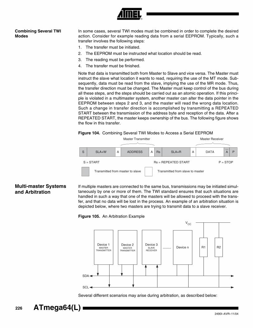
Combining Several TWI Modes
In some cases, several TWI modes must be combined in order to complete the desiredaction. Consider for example reading data from a serial EEPROM. Typically, such atransfer involves the following steps:
1. The transfer must be initiated.
2. The EEPROM must be instructed what location should be read.
3. The reading must be performed.
4. The transfer must be finished.
Note that data is transmitted both from Master to Slave and vice versa. The Master mustinstruct the slave what location it wants to read, requiring the use of the MT mode. Sub-sequently, data must be read from the slave, implying the use of the MR mode. Thus,the transfer direction must be changed. The Master must keep control of the bus duringall these steps, and the steps should be carried out as an atomic operation. If this princi-ple is violated in a multimaster system, another master can alter the data pointer in theEEPROM between steps 2 and 3, and the master will read the wrong data location.Such a change in transfer direction is accomplished by transmitting a REPEATEDSTART between the transmission of the address byte and reception of the data. After aREPEATED START, the master keeps ownership of the bus. The following figure showsthe flow in this transfer.
Figure 104. Combining Several TWI Modes to Access a Serial EEPROM
Multi-master Systems and Arbitration
If multiple masters are connected to the same bus, transmissions may be initiated simul-taneously by one or more of them. The TWI standard ensures that such situations arehandled in such a way that one of the masters will be allowed to proceed with the trans-fer, and that no data will be lost in the process. An example of an arbitration situation isdepicted below, where two masters are trying to transmit data to a slave receiver.
Figure 105. An Arbitration Example
Several different scenarios may arise during arbitration, as described below:
Master Transmitter Master Receiver
S = START Rs = REPEATED START P = STOP
Transmitted from master to slave Transmitted from slave to master
S SLA+W A ADDRESS A Rs SLA+R A DATA A P
Device 1MASTER
TRANSMITTER
Device 2MASTER
TRANSMITTER
Device 3SLAVE
RECEIVERDevice n
SDA
SCL
........ R1 R2
VCC
226 ATmega64(L)2490I–AVR–11/04
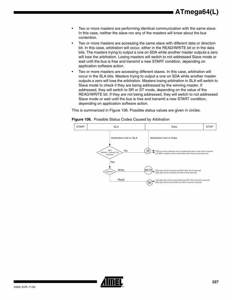
ATmega64(L)
• Two or more masters are performing identical communication with the same slave. In this case, neither the slave nor any of the masters will know about the bus contention.
• Two or more masters are accessing the same slave with different data or direction bit. In this case, arbitration will occur, either in the READ/WRITE bit or in the data bits. The masters trying to output a one on SDA while another master outputs a zero will lose the arbitration. Losing masters will switch to not addressed Slave mode or wait until the bus is free and transmit a new START condition, depending on application software action.
• Two or more masters are accessing different slaves. In this case, arbitration will occur in the SLA bits. Masters trying to output a one on SDA while another master outputs a zero will lose the arbitration. Masters losing arbitration in SLA will switch to Slave mode to check if they are being addressed by the winning master. If addressed, they will switch to SR or ST mode, depending on the value of the READ/WRITE bit. If they are not being addressed, they will switch to not addressed Slave mode or wait until the bus is free and transmit a new START condition, depending on application software action.
This is summarized in Figure 106. Possible status values are given in circles.
Figure 106. Possible Status Codes Caused by Arbitration
OwnAddress / General Call
received
Arbitration lost in SLA
TWI bus will be released and not addressed slave mode will be enteredA START condition will be transmitted when the bus becomes free
No
Arbitration lost in Data
Direction
Yes
Write Data byte will be received and NOT ACK will be returnedData byte will be received and ACK will be returned
Last data byte will be transmitted and NOT ACK should be receivedData byte will be transmitted and ACK should be received
ReadB0
68/78
38
SLASTART Data STOP
2272490I–AVR–11/04
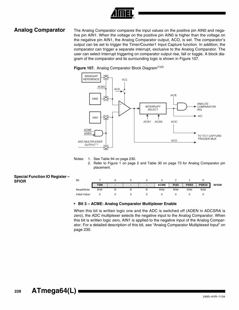
Analog Comparator The Analog Comparator compares the input values on the positive pin AIN0 and nega-tive pin AIN1. When the voltage on the positive pin AIN0 is higher than the voltage onthe negative pin AIN1, the Analog Comparator output, ACO, is set. The comparator’soutput can be set to trigger the Timer/Counter1 Input Capture function. In addition, thecomparator can trigger a separate interrupt, exclusive to the Analog Comparator. Theuser can select Interrupt triggering on comparator output rise, fall or toggle. A block dia-gram of the comparator and its surrounding logic is shown in Figure 107.
Figure 107. Analog Comparator Block Diagram(1)(2)
Notes: 1. See Table 94 on page 230.2. Refer to Figure 1 on page 2 and Table 30 on page 73 for Analog Comparator pin
placement.
Special Function IO Register – SFIOR
• Bit 3 – ACME: Analog Comparator Multiplexer Enable
When this bit is written logic one and the ADC is switched off (ADEN in ADCSRA iszero), the ADC multiplexer selects the negative input to the Analog Comparator. Whenthis bit is written logic zero, AIN1 is applied to the negative input of the Analog Compar-ator. For a detailed description of this bit, see “Analog Comparator Multiplexed Input” onpage 230.
ACBG
BANDGAPREFERENCE
ADC MULTIPLEXEROUTPUT
ACMEADEN
1)
Bit 7 6 5 4 3 2 1 0
TSM – – – ACME PUD PSR2 PSR10 SFIORRead/Write R/W R R R R/W R/W R/W R/W
Initial Value 0 0 0 0 0 0 0 0
228 ATmega64(L)2490I–AVR–11/04
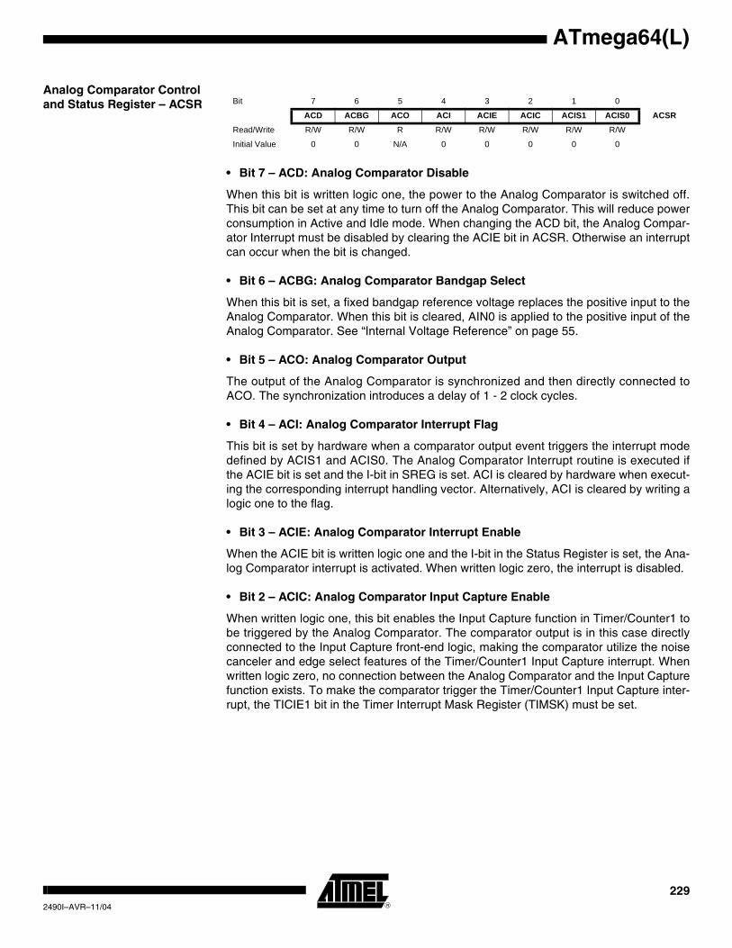
ATmega64(L)
Analog Comparator Control and Status Register – ACSR
• Bit 7 – ACD: Analog Comparator Disable
When this bit is written logic one, the power to the Analog Comparator is switched off.This bit can be set at any time to turn off the Analog Comparator. This will reduce powerconsumption in Active and Idle mode. When changing the ACD bit, the Analog Compar-ator Interrupt must be disabled by clearing the ACIE bit in ACSR. Otherwise an interruptcan occur when the bit is changed.
• Bit 6 – ACBG: Analog Comparator Bandgap Select
When this bit is set, a fixed bandgap reference voltage replaces the positive input to theAnalog Comparator. When this bit is cleared, AIN0 is applied to the positive input of theAnalog Comparator. See “Internal Voltage Reference” on page 55.
• Bit 5 – ACO: Analog Comparator Output
The output of the Analog Comparator is synchronized and then directly connected toACO. The synchronization introduces a delay of 1 - 2 clock cycles.
• Bit 4 – ACI: Analog Comparator Interrupt Flag
This bit is set by hardware when a comparator output event triggers the interrupt modedefined by ACIS1 and ACIS0. The Analog Comparator Interrupt routine is executed ifthe ACIE bit is set and the I-bit in SREG is set. ACI is cleared by hardware when execut-ing the corresponding interrupt handling vector. Alternatively, ACI is cleared by writing alogic one to the flag.
• Bit 3 – ACIE: Analog Comparator Interrupt Enable
When the ACIE bit is written logic one and the I-bit in the Status Register is set, the Ana-log Comparator interrupt is activated. When written logic zero, the interrupt is disabled.
• Bit 2 – ACIC: Analog Comparator Input Capture Enable
When written logic one, this bit enables the Input Capture function in Timer/Counter1 tobe triggered by the Analog Comparator. The comparator output is in this case directlyconnected to the Input Capture front-end logic, making the comparator utilize the noisecanceler and edge select features of the Timer/Counter1 Input Capture interrupt. Whenwritten logic zero, no connection between the Analog Comparator and the Input Capturefunction exists. To make the comparator trigger the Timer/Counter1 Input Capture inter-rupt, the TICIE1 bit in the Timer Interrupt Mask Register (TIMSK) must be set.
Bit 7 6 5 4 3 2 1 0
ACD ACBG ACO ACI ACIE ACIC ACIS1 ACIS0 ACSRRead/Write R/W R/W R R/W R/W R/W R/W R/W
Initial Value 0 0 N/A 0 0 0 0 0
2292490I–AVR–11/04
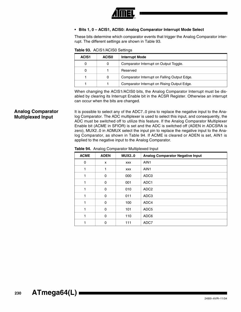
• Bits 1, 0 – ACIS1, ACIS0: Analog Comparator Interrupt Mode Select
These bits determine which comparator events that trigger the Analog Comparator inter-rupt. The different settings are shown in Table 93.
When changing the ACIS1/ACIS0 bits, the Analog Comparator Interrupt must be dis-abled by clearing its Interrupt Enable bit in the ACSR Register. Otherwise an interruptcan occur when the bits are changed.
Analog Comparator Multiplexed Input
It is possible to select any of the ADC7..0 pins to replace the negative input to the Ana-log Comparator. The ADC multiplexer is used to select this input, and consequently, theADC must be switched off to utilize this feature. If the Analog Comparator MultiplexerEnable bit (ACME in SFIOR) is set and the ADC is switched off (ADEN in ADCSRA iszero), MUX2..0 in ADMUX select the input pin to replace the negative input to the Ana-log Comparator, as shown in Table 94. If ACME is cleared or ADEN is set, AIN1 isapplied to the negative input to the Analog Comparator.
Table 93. ACIS1/ACIS0 Settings
ACIS1 ACIS0 Interrupt Mode
0 0 Comparator Interrupt on Output Toggle.
0 1 Reserved
1 0 Comparator Interrupt on Falling Output Edge.
1 1 Comparator Interrupt on Rising Output Edge.
Table 94. Analog Comparator Multiplexed Input
ACME ADEN MUX2..0 Analog Comparator Negative Input
0 x xxx AIN1
1 1 xxx AIN1
1 0 000 ADC0
1 0 001 ADC1
1 0 010 ADC2
1 0 011 ADC3
1 0 100 ADC4
1 0 101 ADC5
1 0 110 ADC6
1 0 111 ADC7
230 ATmega64(L)2490I–AVR–11/04
ATmega64(L)
Analog to Digital Converter
Features • 10-bit Resolution• 0.75 LSB Integral Non-linearity• ±1.5 LSB Absolute Accuracy• 13 - 260 µs Conversion Time• Up to 15 kSPS at Maximum Resolution• Eight Multiplexed Single Ended Input Channels• Seven Differential Input Channels• Two Differential Input Channels with Optional Gain of 10x and 200x• Optional Left Adjustment for ADC Result Readout• 0 - VCC ADC Input Voltage Range• Selectable 2.56V ADC Reference Voltage• Free Running or Single Conversion Mode• ADC Start Conversion by Auto Triggering on Interrupt Sources• Interrupt on ADC Conversion Complete• Sleep Mode Noise Canceler
The ATmega64 features a 10-bit successive approximation ADC. The ADC is con-nected to an 8-channel Analog Multiplexer which allows eight single-ended voltageinputs constructed from the pins of Port F. The single-ended voltage inputs refer to 0V(GND).
The device also supports 16 differential voltage input combinations. Two of the differen-tial inputs (ADC1, ADC0 and ADC3, ADC2) are equipped with a programmable gainstage, providing amplification steps of 0 dB (1x), 20 dB (10x), or 46 dB (200x) on the dif-ferential input voltage before the A/D conversion. Seven differential analog inputchannels share a common negative terminal (ADC1), while any other ADC input can beselected as the positive input terminal. If 1x or 10x gain is used, 8-bit resolution can beexpected. If 200x gain is used, 7-bit resolution can be expected.
The ADC contains a Sample and Hold circuit which ensures that the input voltage to theADC is held at a constant level during conversion. A block diagram of the ADC is shownin Figure 108.
The ADC has a separate analog supply voltage pin, AVCC. AVCC must not differ morethan ±0.3V from VCC. See the paragraph “ADC Noise Canceler” on page 239 on how toconnect this pin.
Internal reference voltages of nominally 2.56V or AVCC are provided On-chip. The volt-age reference may be externally decoupled at the AREF pin by a capacitor for betternoise performance.
2312490I–AVR–11/04
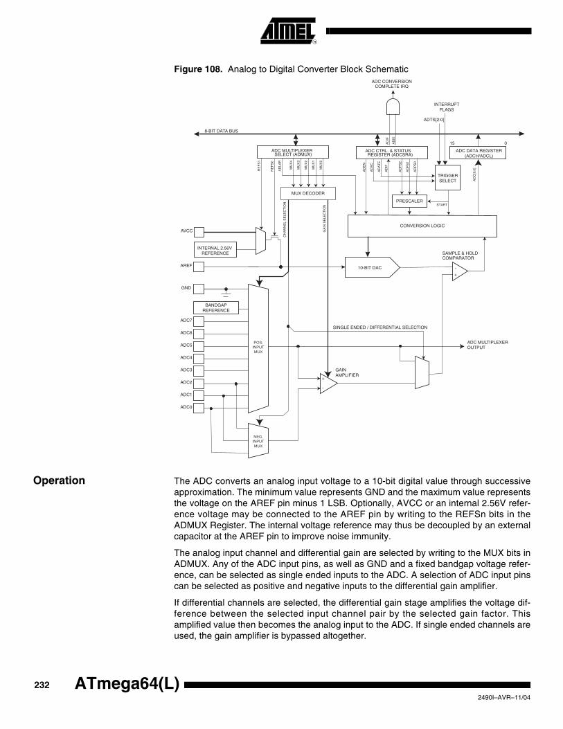
Figure 108. Analog to Digital Converter Block Schematic
Operation The ADC converts an analog input voltage to a 10-bit digital value through successiveapproximation. The minimum value represents GND and the maximum value representsthe voltage on the AREF pin minus 1 LSB. Optionally, AVCC or an internal 2.56V refer-ence voltage may be connected to the AREF pin by writing to the REFSn bits in theADMUX Register. The internal voltage reference may thus be decoupled by an externalcapacitor at the AREF pin to improve noise immunity.
The analog input channel and differential gain are selected by writing to the MUX bits inADMUX. Any of the ADC input pins, as well as GND and a fixed bandgap voltage refer-ence, can be selected as single ended inputs to the ADC. A selection of ADC input pinscan be selected as positive and negative inputs to the differential gain amplifier.
If differential channels are selected, the differential gain stage amplifies the voltage dif-ference between the selected input channel pair by the selected gain factor. Thisamplified value then becomes the analog input to the ADC. If single ended channels areused, the gain amplifier is bypassed altogether.
ADC CONVERSIONCOMPLETE IRQ
8-BIT DATA BUS
15 0
ADC MULTIPLEXERSELECT (ADMUX)
ADC CTRL. & STATUSREGISTER (ADCSRA)
ADC DATA REGISTER(ADCH/ADCL)
MU
X2
AD
IE
AD
AT
E
AD
SC
AD
EN
AD
IFA
DIF
MU
X1
MU
X0
AD
PS
0
AD
PS
1
AD
PS
2
MU
X3
CONVERSION LOGIC
10-BIT DAC
+-
SAMPLE & HOLDCOMPARATOR
INTERNAL 2.56V REFERENCE
MUX DECODER
MU
X4
AVCC
ADC7
ADC6
ADC5
ADC4
ADC3
ADC2
ADC1
ADC0
RE
FS
0
RE
FS
1
AD
LAR
+
-
CH
AN
NE
L S
ELE
CT
ION
GA
IN S
ELE
CT
ION
AD
C[9
:0]
ADC MULTIPLEXEROUTPUT
GAINAMPLIFIER
AREF
BANDGAPREFERENCE
PRESCALER
SINGLE ENDED / DIFFERENTIAL SELECTION
GND
POS.INPUTMUX
NEG.INPUTMUX
TRIGGERSELECT
ADTS[2:0]
INTERRUPTFLAGS
START
232 ATmega64(L)2490I–AVR–11/04
ATmega64(L)
The ADC is enabled by setting the ADC Enable bit, ADEN in ADCSRA. Voltage refer-ence and input channel selections will not go into effect until ADEN is set. The ADCdoes not consume power when ADEN is cleared, so it is recommended to switch off theADC before entering power saving sleep modes.
The ADC generates a 10-bit result which is presented in the ADC Data Registers,ADCH and ADCL. By default, the result is presented right adjusted, but can optionallybe presented left adjusted by setting the ADLAR bit in ADMUX.
If the result is left adjusted and no more than 8-bit precision is required, it is sufficient toread ADCH. Otherwise, ADCL must be read first, then ADCH, to ensure that the contentof the data registers belongs to the same conversion. Once ADCL is read, ADC accessto data registers is blocked. This means that if ADCL has been read, and a conversioncompletes before ADCH is read, neither register is updated and the result from the con-version is lost. When ADCH is read, ADC access to the ADCH and ADCL Registers isre-enabled.
The ADC has its own interrupt which can be triggered when a conversion completes.When ADC access to the data registers is prohibited between reading of ADCH andADCL, the interrupt will trigger even if the result is lost.
Starting a Conversion A single conversion is started by writing a logical one to the ADC Start Conversion bit,ADSC. This bit stays high as long as the conversion is in progress and will be cleared byhardware when the conversion is completed. If a different data channel is selected whilea conversion is in progress, the ADC will finish the current conversion before performingthe channel change.
Alternatively, a conversion can be triggered automatically by various sources. Auto Trig-gering is enabled by setting the ADC Auto Trigger Enable bit, ADATE in ADCSRA. Thetrigger source is selected by setting the ADC Trigger Select bits, ADTS in ADCSRB (seedescription of the ADTS bits for a list of the trigger sources). When a positive edgeoccurs on the selected trigger signal, the ADC prescaler is reset and a conversion isstarted. This provides a method of starting conversions at fixed intervals. If the triggersignal still is set when the conversion completes, a new conversion will not be started. Ifanother positive edge occurs on the trigger signal during conversion, the edge will beignored. Note that an interrupt flag will be set even if the specific interrupt is disabled orthe Global Interrupt Enable bit in SREG is cleared. A conversion can thus be triggeredwithout causing an interrupt. However, the interrupt flag must be cleared in order to trig-ger a new conversion at the next interrupt event.
2332490I–AVR–11/04
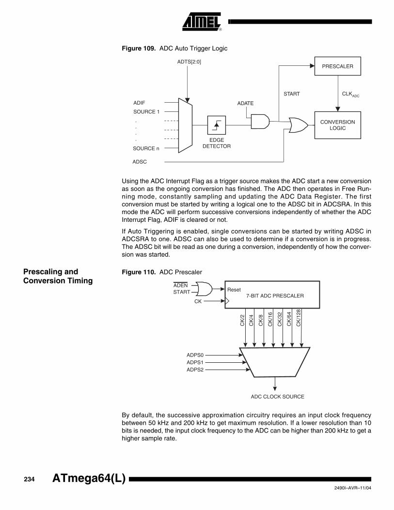
Figure 109. ADC Auto Trigger Logic
Using the ADC Interrupt Flag as a trigger source makes the ADC start a new conversionas soon as the ongoing conversion has finished. The ADC then operates in Free Run-ning mode, constantly sampling and updating the ADC Data Register. The firstconversion must be started by writing a logical one to the ADSC bit in ADCSRA. In thismode the ADC will perform successive conversions independently of whether the ADCInterrupt Flag, ADIF is cleared or not.
If Auto Triggering is enabled, single conversions can be started by writing ADSC inADCSRA to one. ADSC can also be used to determine if a conversion is in progress.The ADSC bit will be read as one during a conversion, independently of how the conver-sion was started.
Prescaling and Conversion Timing
Figure 110. ADC Prescaler
By default, the successive approximation circuitry requires an input clock frequencybetween 50 kHz and 200 kHz to get maximum resolution. If a lower resolution than 10bits is needed, the input clock frequency to the ADC can be higher than 200 kHz to get ahigher sample rate.
ADSC
ADIF
SOURCE 1
SOURCE n
ADTS[2:0]
CONVERSIONLOGIC
PRESCALER
START CLKADC
.
.
.
. EDGEDETECTOR
ADATE
7-BIT ADC PRESCALER
ADC CLOCK SOURCE
CK
ADPS0ADPS1ADPS2
CK
/128
CK
/2
CK
/4
CK
/8
CK
/16
CK
/32
CK
/64
ResetADENSTART
234 ATmega64(L)2490I–AVR–11/04
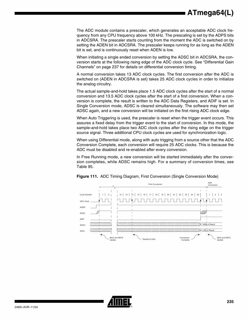
ATmega64(L)
The ADC module contains a prescaler, which generates an acceptable ADC clock fre-quency from any CPU frequency above 100 kHz. The prescaling is set by the ADPS bitsin ADCSRA. The prescaler starts counting from the moment the ADC is switched on bysetting the ADEN bit in ADCSRA. The prescaler keeps running for as long as the ADENbit is set, and is continuously reset when ADEN is low.
When initiating a single ended conversion by setting the ADSC bit in ADCSRA, the con-version starts at the following rising edge of the ADC clock cycle. See “Differential GainChannels” on page 237 for details on differential conversion timing.
A normal conversion takes 13 ADC clock cycles. The first conversion after the ADC isswitched on (ADEN in ADCSRA is set) takes 25 ADC clock cycles in order to initializethe analog circuitry.
The actual sample-and-hold takes place 1.5 ADC clock cycles after the start of a normalconversion and 13.5 ADC clock cycles after the start of a first conversion. When a con-version is complete, the result is written to the ADC Data Registers, and ADIF is set. InSingle Conversion mode, ADSC is cleared simultaneously. The software may then setADSC again, and a new conversion will be initiated on the first rising ADC clock edge.
When Auto Triggering is used, the prescaler is reset when the trigger event occurs. Thisassures a fixed delay from the trigger event to the start of conversion. In this mode, thesample-and-hold takes place two ADC clock cycles after the rising edge on the triggersource signal. Three additional CPU clock cycles are used for synchronization logic.
When using Differential mode, along with auto trigging from a source other that the ADCConversion Complete, each conversion will require 25 ADC clocks. This is because theADC must be disabled and re-enabled after every conversion.
In Free Running mode, a new conversion will be started immediately after the conver-sion completes, while ADSC remains high. For a summary of conversion times, seeTable 95.
Figure 111. ADC Timing Diagram, First Conversion (Single Conversion Mode)
MSB of Result
LSB of Result
ADC Clock
ADSC
Sample & Hold
ADIF
ADCH
ADCL
Cycle Number
ADEN
1 2 12 13 14 15 16 17 18 19 20 21 22 23 24 25 1 2
First ConversionNextConversion
3
MUX and REFSUpdate
MUX and REFSUpdate
ConversionComplete
2352490I–AVR–11/04
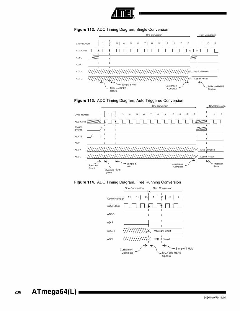
Figure 112. ADC Timing Diagram, Single Conversion
Figure 113. ADC Timing Diagram, Auto Triggered Conversion
Figure 114. ADC Timing Diagram, Free Running Conversion
1 2 3 4 5 6 7 8 9 10 11 12 13
MSB of Result
LSB of Result
ADC Clock
ADSC
ADIF
ADCH
ADCL
Cycle Number 1 2
One Conversion Next Conversion
3
Sample & Hold
MUX and REFSUpdate
ConversionComplete
MUX and REFSUpdate
1 2 3 4 5 6 7 8 9 10 11 12 13
MSB of Result
LSB of Result
ADC Clock
TriggerSource
ADIF
ADCH
ADCL
Cycle Number 1 2
One Conversion Next Conversion
ConversionCompletePrescaler
Reset
ADATE
PrescalerReset
Sample &Hold
MUX and REFS Update
11 12 13
MSB of Result
LSB of Result
ADC Clock
ADSC
ADIF
ADCH
ADCL
Cycle Number1 2
One Conversion Next Conversion
3 4
ConversionComplete
Sample & Hold
MUX and REFSUpdate
236 ATmega64(L)2490I–AVR–11/04
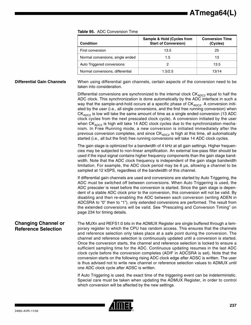
ATmega64(L)
Differential Gain Channels When using differential gain channels, certain aspects of the conversion need to betaken into consideration.
Differential conversions are synchronized to the internal clock CKADC2 equal to half theADC clock. This synchronization is done automatically by the ADC interface in such away that the sample-and-hold occurs at a specific phase of CKADC2. A conversion initi-ated by the user (i.e., all single conversions, and the first free running conversion) whenCKADC2 is low will take the same amount of time as a single ended conversion (13 ADCclock cycles from the next prescaled clock cycle). A conversion initiated by the userwhen CKADC2 is high will take 14 ADC clock cycles due to the synchronization mecha-nism. In Free Running mode, a new conversion is initiated immediately after theprevious conversion completes, and since CKADC2 is high at this time, all automaticallystarted (i.e., all but the first) free running conversions will take 14 ADC clock cycles.
The gain stage is optimized for a bandwidth of 4 kHz at all gain settings. Higher frequen-cies may be subjected to non-linear amplification. An external low-pass filter should beused if the input signal contains higher frequency components than the gain stage band-width. Note that the ADC clock frequency is independent of the gain stage bandwidthlimitation. For example, the ADC clock period may be 6 µs, allowing a channel to besampled at 12 kSPS, regardless of the bandwidth of this channel.
If differential gain channels are used and conversions are started by Auto Triggering, theADC must be switched off between conversions. When Auto Triggering is used, theADC prescaler is reset before the conversion is started. Since the gain stage is depen-dent of a stable ADC clock prior to the conversion, this conversion will not be valid. Bydisabling and then re-enabling the ADC between each conversion (writing ADEN inADCSRA to “0” then to “1”), only extended conversions are performed. The result fromthe extended conversions will be valid. See “Prescaling and Conversion Timing” onpage 234 for timing details.
Changing Channel or Reference Selection
The MUXn and REFS1:0 bits in the ADMUX Register are single buffered through a tem-porary register to which the CPU has random access. This ensures that the channelsand reference selection only takes place at a safe point during the conversion. Thechannel and reference selection is continuously updated until a conversion is started.Once the conversion starts, the channel and reference selection is locked to ensure asufficient sampling time for the ADC. Continuous updating resumes in the last ADCclock cycle before the conversion completes (ADIF in ADCSRA is set). Note that theconversion starts on the following rising ADC clock edge after ADSC is written. The useris thus advised not to write new channel or reference selection values to ADMUX untilone ADC clock cycle after ADSC is written.
If Auto Triggering is used, the exact time of the triggering event can be indeterministic.Special care must be taken when updating the ADMUX Register, in order to controlwhich conversion will be affected by the new settings.
Table 95. ADC Conversion Time
ConditionSample & Hold (Cycles from
Start of Conversion)Conversion Time
(Cycles)
First conversion 13.5 25
Normal conversions, single ended 1.5 13
Auto Triggered conversions 2 13.5
Normal conversions, differential 1.5/2.5 13/14
2372490I–AVR–11/04
If both ADATE and ADEN is written to one, an interrupt event can occur at any time. Ifthe ADMUX Register is changed in this period, the user cannot tell if the next conversionis based on the old or the new settings. ADMUX can be safely updated in the followingways:
1. When ADATE or ADEN is cleared.
2. During conversion, minimum one ADC clock cycle after the trigger event.
3. After a conversion, before the interrupt flag used as trigger source is cleared.
When updating ADMUX in one of these conditions, the new settings will affect the nextADC conversion.
Special care should be taken when changing differential channels. Once a differentialchannel has been selected, the gain stage may take as much as 125 µs to stabilize tothe new value. Thus conversions should not be started within the first 125 µs afterselecting a new differential channel. Alternatively, conversion results obtained within thisperiod should be discarded.
The same settling time should be observed for the first differential conversion afterchanging ADC reference (by changing the REFS1:0 bits in ADMUX).
If the JTAG interface is enabled, the function of ADC channels on PORTF7:4 is overrid-den. Refer to Table 42, “Port F Pins Alternate Functions,” on page 82.
ADC Input Channels When changing channel selections, the user should observe the following guidelines toensure that the correct channel is selected:
In Single Conversion mode, always select the channel before starting the conversion.The channel selection may be changed one ADC clock cycle after writing one to ADSC.However, the simplest method is to wait for the conversion to complete before changingthe channel selection.
In Free Running mode, always select the channel before starting the first conversion.The channel selection may be changed one ADC clock cycle after writing one to ADSC.However, the simplest method is to wait for the first conversion to complete, and thenchange the channel selection. Since the next conversion has already started automati-cally, the next result will reflect the previous channel selection. Subsequent conversionswill reflect the new channel selection.
When switching to a differential gain channel, the first conversion result may have apoor accuracy due to the required settling time for the automatic offset cancellation cir-cuitry. The user should preferably disregard the first conversion result.
ADC Voltage Reference The reference voltage for the ADC (VREF) indicates the conversion range for the ADC.Single ended channels that exceed VREF will result in codes close to 0x3FF. VREF can beselected as either AVCC, internal 2.56V reference, or external AREF pin.
AVCC is connected to the ADC through a passive switch. The internal 2.56V referenceis generated from the internal bandgap reference (VBG) through an internal amplifier. Ineither case, the external AREF pin is directly connected to the ADC, and the referencevoltage can be made more immune to noise by connecting a capacitor between theAREF pin and ground. VREF can also be measured at the AREF pin with a high impedantvoltmeter. Note that VREF is a high impedant source, and only a capacitive load shouldbe connected in a system.
If the user has a fixed voltage source connected to the AREF pin, the user may not usethe other reference voltage options in the application, as they will be shorted to theexternal voltage. If no external voltage is applied to the AREF pin, the user may switch
238 ATmega64(L)2490I–AVR–11/04
ATmega64(L)
between AVCC and 2.56V as reference selection. The first ADC conversion result afterswitching reference voltage source may be inaccurate, and the user is advised to dis-card this result.
If differential channels are used, the selected reference should not be closer to AVCCthan indicated in Table 136 on page 335.
ADC Noise Canceler The ADC features a noise canceler that enables conversion during sleep mode toreduce noise induced from the CPU core and other I/O peripherals. The noise cancelercan be used with ADC Noise Reduction and Idle mode. To make use of this feature, thefollowing procedure should be used:
1. Make sure that the ADC is enabled and is not busy converting. Single Con-version mode must be selected and the ADC conversion complete interruptmust be enabled.
2. Enter ADC Noise Reduction mode (or Idle mode). The ADC will start a con-version once the CPU has been halted.
3. If no other interrupts occur before the ADC conversion completes, the ADCinterrupt will wake up the CPU and execute the ADC Conversion Completeinterrupt routine. If another interrupt wakes up the CPU before the ADC con-version is complete, that interrupt will be executed, and an ADC ConversionComplete interrupt request will be generated when the ADC conversioncompletes. The CPU will remain in Active mode until a new sleep commandis executed.
Note that the ADC will not be automatically turned off when entering other sleep modesthan Idle mode and ADC Noise Reduction mode. The user is advised to write zero toADEN before entering such sleep modes to avoid excessive power consumption. If theADC is enabled in such sleep modes and the user wants to perform differential conver-sions, the user is advised to switch the ADC off and on after waking up from sleep toprompt an extended conversion to get a valid result.
Analog Input Circuitry The analog input circuitry for single ended channels is illustrated in Figure 115. An ana-log source applied to ADCn is subjected to the pin capacitance and input leakage of thatpin, regardless of whether that channel is selected as input for the ADC. When the chan-nel is selected, the source must drive the S/H capacitor through the series resistance(combined resistance in the input path).
The ADC is optimized for analog signals with an output impedance of approximately10 kΩ or less. If such a source is used, the sampling time will be negligible. If a sourcewith higher impedance is used, the sampling time will depend on how long time thesource needs to charge the S/H capacitor, with can vary widely. The user is recom-mended to only use low impedant sources with slowly varying signals, since thisminimizes the required charge transfer to the S/H capacitor.
If differential gain channels are used, the input circuitry looks somewhat different,although source impedances of a few hundred kΩ or less is recommended.
Signal components higher than the Nyquist frequency (fADC/2) should not be present foreither kind of channels, to avoid distortion from unpredictable signal convolution. Theuser is advised to remove high frequency components with a low-pass filter beforeapplying the signals as inputs to the ADC.
2392490I–AVR–11/04
Figure 115. Analog Input Circuitry
Analog Noise Canceling Techniques
Digital circuitry inside and outside the device generates EMI which might affect theaccuracy of analog measurements. If conversion accuracy is critical, the noise level canbe reduced by applying the following techniques:
1. Keep analog signal paths as short as possible. Make sure analog tracks runover the ground plane, and keep them well away from high-speed switchingdigital tracks.
2. The AVCC pin on the device should be connected to the digital VCC supply voltage via an LC network as shown in Figure 116.
3. Use the ADC noise canceler function to reduce induced noise from the CPU.
4. If any ADC port pins are used as digital outputs, it is essential that these do not switch while a conversion is in progress.
Figure 116. ADC Power Connections
ADCn
IIH
1..100 kΩCS/H= 14 pF
VCC/2
IIL
VCC
GND
100 nF
(ADC0) PF0
(ADC7) PF7
(ADC1) PF1
(ADC2) PF2
(ADC3) PF3
(ADC4) PF4
(ADC5) PF5
(ADC6) PF6
AREF
GND
AVCC
52
53
54
55
56
57
58
59
60
6161
6262
6363
6464
1
51
PE
N
(AD0) PA0
10 µΗ
240 ATmega64(L)2490I–AVR–11/04
ATmega64(L)
Offset Compensation Schemes
The gain stage has a built-in offset cancellation circuitry that nulls the offset of differen-tial measurements as much as possible. The remaining offset in the analog path can bemeasured directly by selecting the same channel for both differential inputs. This offsetresidue can be then subtracted in software from the measurement results. Using thiskind of software based offset correction, offset on any channel can be reduced belowone LSB.
ADC Accuracy Definitions An n-bit single-ended ADC converts a voltage linearly between GND and VREF in 2n
steps (LSBs). The lowest code is read as 0, and the highest code is read as 2n - 1.
Several parameters describe the deviation from the ideal behavior:
• Offset: The deviation of the first transition (0x000 to 0x001) compared to the ideal transition (at 0.5 LSB). Ideal value: 0 LSB.
Figure 117. Offset Error
• Gain Error: After adjusting for offset, the Gain Error is found as the deviation of the last transition (0x3FE to 0x3FF) compared to the ideal transition (at 1.5 LSB below maximum). Ideal value: 0 LSB
Figure 118. Gain Error
Output Code
VREF Input Voltage
Ideal ADC
Actual ADC
OffsetError
Output Code
VREF Input Voltage
Ideal ADC
Actual ADC
GainError
2412490I–AVR–11/04
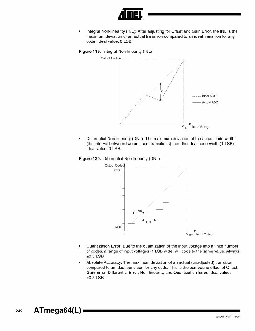
• Integral Non-linearity (INL): After adjusting for Offset and Gain Error, the INL is the maximum deviation of an actual transition compared to an ideal transition for any code. Ideal value: 0 LSB.
Figure 119. Integral Non-linearity (INL)
• Differential Non-linearity (DNL): The maximum deviation of the actual code width (the interval between two adjacent transitions) from the ideal code width (1 LSB). Ideal value: 0 LSB.
Figure 120. Differential Non-linearity (DNL)
• Quantization Error: Due to the quantization of the input voltage into a finite number of codes, a range of input voltages (1 LSB wide) will code to the same value. Always ±0.5 LSB.
• Absolute Accuracy: The maximum deviation of an actual (unadjusted) transition compared to an ideal transition for any code. This is the compound effect of Offset, Gain Error, Differential Error, Non-linearity, and Quantization Error. Ideal value: ±0.5 LSB.
Output Code
VREF Input Voltage
Ideal ADC
Actual ADC
INL
Output Code
0x3FF
0x000
0 VREF Input Voltage
DNL
1 LSB
242 ATmega64(L)2490I–AVR–11/04
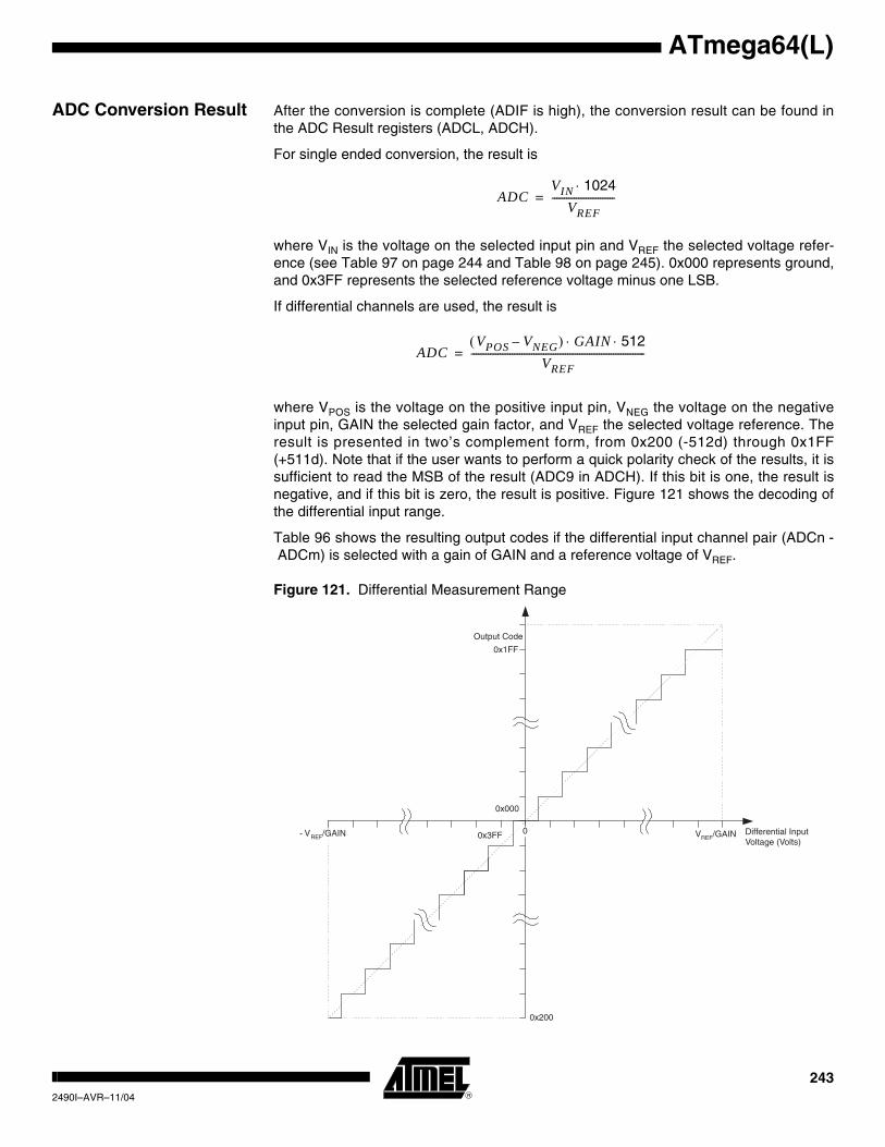
ATmega64(L)
ADC Conversion Result After the conversion is complete (ADIF is high), the conversion result can be found inthe ADC Result registers (ADCL, ADCH).
For single ended conversion, the result is
where VIN is the voltage on the selected input pin and VREF the selected voltage refer-ence (see Table 97 on page 244 and Table 98 on page 245). 0x000 represents ground,and 0x3FF represents the selected reference voltage minus one LSB.
If differential channels are used, the result is
where VPOS is the voltage on the positive input pin, VNEG the voltage on the negativeinput pin, GAIN the selected gain factor, and VREF the selected voltage reference. Theresult is presented in two’s complement form, from 0x200 (-512d) through 0x1FF(+511d). Note that if the user wants to perform a quick polarity check of the results, it issufficient to read the MSB of the result (ADC9 in ADCH). If this bit is one, the result isnegative, and if this bit is zero, the result is positive. Figure 121 shows the decoding ofthe differential input range.
Table 96 shows the resulting output codes if the differential input channel pair (ADCn -ADCm) is selected with a gain of GAIN and a reference voltage of VREF.
Figure 121. Differential Measurement Range
ADCVIN 1024⋅
VREF--------------------------=
ADCVPOS VNEG–( ) GAIN 512⋅ ⋅
VREF------------------------------------------------------------------------=
0
Output Code
0x1FF
0x000
VREF/GAIN Differential InputVoltage (Volts)
0x3FF
0x200
- VREF/GAIN
2432490I–AVR–11/04
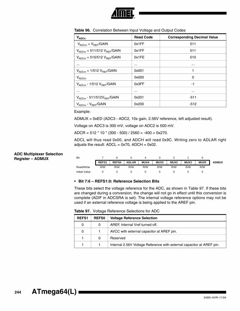
Example:
ADMUX = 0xED (ADC3 - ADC2, 10x gain, 2.56V reference, left adjusted result).
Voltage on ADC3 is 300 mV, voltage on ADC2 is 500 mV.
ADCR = 512 * 10 * (300 - 500) / 2560 = -400 = 0x270.
ADCL will thus read 0x00, and ADCH will read 0x9C. Writing zero to ADLAR rightadjusts the result: ADCL = 0x70, ADCH = 0x02.
ADC Multiplexer Selection Register – ADMUX
• Bit 7:6 – REFS1:0: Reference Selection Bits
These bits select the voltage reference for the ADC, as shown in Table 97. If these bitsare changed during a conversion, the change will not go in effect until this conversion iscomplete (ADIF in ADCSRA is set). The internal voltage reference options may not beused if an external reference voltage is being applied to the AREF pin.
Table 96. Correlation Between Input Voltage and Output Codes
VADCn Read Code Corresponding Decimal Value
VADCm + VREF/GAIN 0x1FF 511
VADCm + 511/512 VREF/GAIN 0x1FF 511
VADCm + 510/512 VREF/GAIN 0x1FE 510
... ... ...
VADCm + 1/512 VREF/GAIN 0x001 1
VADCm 0x000 0
VADCm - 1/512 VREF/GAIN 0x3FF -1
... ... ...
VADCm - 511/512VREF/GAIN 0x201 -511
VADCm - VREF/GAIN 0x200 -512
Bit 7 6 5 4 3 2 1 0
REFS1 REFS0 ADLAR MUX4 MUX3 MUX2 MUX1 MUX0 ADMUXRead/Write R/W R/W R/W R/W R/W R/W R/W R/W
Initial Value 0 0 0 0 0 0 0 0
Table 97. Voltage Reference Selections for ADC
REFS1 REFS0 Voltage Reference Selection
0 0 AREF, Internal Vref turned off.
0 1 AVCC with external capacitor at AREF pin.
1 0 Reserved
1 1 Internal 2.56V Voltage Reference with external capacitor at AREF pin.
244 ATmega64(L)2490I–AVR–11/04
ATmega64(L)
• Bit 5 – ADLAR: ADC Left Adjust Result
The ADLAR bit affects the presentation of the ADC conversion result in the ADC DataRegister. Write one to ADLAR to left adjust the result. Otherwise, the result is rightadjusted. Changing the ADLAR bit will affect the ADC Data Register immediately,regardless of any ongoing conversions. For a complete description of this bit, see “TheADC Data Register – ADCL and ADCH” on page 247.
• Bits 4:0 – MUX4:0: Analog Channel and Gain Selection Bits
The value of these bits selects which combination of analog inputs are connected to theADC. These bits also select the gain for the differential channels. See Table 98 fordetails. If these bits are changed during a conversion, the change will not go in effectuntil this conversion is complete (ADIF in ADCSRA is set).
Table 98. Input Channel and Gain Selections
MUX4..0 Single Ended InputPositive Differential Input
Negative Differential Input Gain
00000 ADC0
00001 ADC1
00010 ADC2
00011 ADC3 N/A
00100 ADC4
00101 ADC5
00110 ADC6
00111 ADC7
01000 ADC0 ADC0 10x
01001 ADC1 ADC0 10x
01010 ADC0 ADC0 200x
01011 ADC1 ADC0 200x
01100 ADC2 ADC2 10x
01101 ADC3 ADC2 10x
01110 ADC2 ADC2 200x
01111 ADC3 ADC2 200x
10000 ADC0 ADC1 1x
10001 ADC1 ADC1 1x
10010 N/A ADC2 ADC1 1x
10011 ADC3 ADC1 1x
10100 ADC4 ADC1 1x
10101 ADC5 ADC1 1x
10110 ADC6 ADC1 1x
10111 ADC7 ADC1 1x
11000 ADC0 ADC2 1x
11001 ADC1 ADC2 1x
2452490I–AVR–11/04
ADC Control and Status Register A – ADCSRA
• Bit 7 – ADEN: ADC Enable
Writing this bit to one enables the ADC. By writing it to zero, the ADC is turned off. Turn-ing the ADC off while a conversion is in progress, will terminate this conversion.
• Bit 6 – ADSC: ADC Start Conversion
In Single Conversion mode, write this bit to one to start each conversion. In Free Run-ning mode, write this bit to one to start the first conversion. The first conversion afterADSC has been written after the ADC has been enabled, or if ADSC is written at thesame time as the ADC is enabled, will take 25 ADC clock cycles instead of the normal13. This first conversion performs initialization of the ADC.
ADSC will read as one as long as a conversion is in progress. When the conversion iscomplete, it returns to zero. Writing zero to this bit has no effect.
• Bit 5 – ADATE: ADC Auto Trigger Enable
When this bit is written to one, Auto Triggering of the ADC is enabled. The ADC will starta conversion on a positive edge of the selected trigger signal. The trigger source isselected by setting the ADC Trigger Select bits, ADTS in ADCSRB.
• Bit 4 – ADIF: ADC Interrupt Flag
This bit is set when an ADC conversion completes and the data registers are updated.The ADC Conversion Complete Interrupt is executed if the ADIE bit and the I-bit inSREG are set. ADIF is cleared by hardware when executing the corresponding interrupthandling vector. Alternatively, ADIF is cleared by writing a logical one to the flag.Beware that if doing a Read-Modify-Write on ADCSRA, a pending interrupt can be dis-abled. This also applies if the SBI and CBI instructions are used.
• Bit 3 – ADIE: ADC Interrupt Enable
When this bit is written to one and the I-bit in SREG is set, the ADC Conversion Com-plete Interrupt is activated.
11010 ADC2 ADC2 1x
11011 ADC3 ADC2 1x
11100 ADC4 ADC2 1x
11101 ADC5 ADC2 1x
11110 1.22V (VBG) N/A
11111 0V (GND)
Table 98. Input Channel and Gain Selections (Continued)
MUX4..0 Single Ended InputPositive Differential Input
Negative Differential Input Gain
Bit 7 6 5 4 3 2 1 0
ADEN ADSC ADATE ADIF ADIE ADPS2 ADPS1 ADPS0 ADCSRARead/Write R/W R/W R/W R/W R/W R/W R/W R/W
Initial Value 0 0 0 0 0 0 0 0
246 ATmega64(L)2490I–AVR–11/04
ATmega64(L)
• Bits 2:0 – ADPS2:0: ADC Prescaler Select Bits
These bits determine the division factor between the XTAL frequency and the inputclock to the ADC.
The ADC Data Register – ADCL and ADCH
ADLAR = 0
ADLAR = 1
When an ADC conversion is complete, the result is found in these two registers. If differ-ential channels are used, the result is presented in two’s complement form.
When ADCL is read, the ADC Data Register is not updated until ADCH is read. Conse-quently, if the result is left adjusted and no more than 8-bit precision is required, it issufficient to read ADCH. Otherwise, ADCL must be read first, then ADCH.
The ADLAR bit in ADMUX, and the MUXn bits in ADMUX affect the way the result isread from the registers. If ADLAR is set, the result is left adjusted. If ADLAR is cleared(default), the result is right adjusted.
Table 99. ADC Prescaler Selections
ADPS2 ADPS1 ADPS0 Division Factor
0 0 0 2
0 0 1 2
0 1 0 4
0 1 1 8
1 0 0 16
1 0 1 32
1 1 0 64
1 1 1 128
Bit 15 14 13 12 11 10 9 8
– – – – – – ADC9 ADC8 ADCHADC7 ADC6 ADC5 ADC4 ADC3 ADC2 ADC1 ADC0 ADCL
7 6 5 4 3 2 1 0
Read/Write R R R R R R R R
R R R R R R R R
Initial Value 0 0 0 0 0 0 0 0
0 0 0 0 0 0 0 0
Bit 15 14 13 12 11 10 9 8
ADC9 ADC8 ADC7 ADC6 ADC5 ADC4 ADC3 ADC2 ADCHADC1 ADC0 – – – – – – ADCL
7 6 5 4 3 2 1 0
Read/Write R R R R R R R R
R R R R R R R R
Initial Value 0 0 0 0 0 0 0 0
0 0 0 0 0 0 0 0
2472490I–AVR–11/04
• ADC9:0: ADC Conversion Result
These bits represent the result from the conversion, as detailed in “ADC ConversionResult” on page 243.
ADC Control and Status Register B – ADCSRB
• Bits 7:3 – Res: Reserved Bits
These bits are reserved bits in the ATmega64 and will always read as zero.
• Bit 2:0 – ADTS2:0: ADC Auto Trigger Source
If ADATE in ADCSRA is written to one, the value of these bits selects which source willtrigger an ADC conversion. If ADATE is cleared, the ADTS2:0 settings will have noeffect. A conversion will be triggered by the rising edge of the selected interrupt flag.Note that switching from a trigger source that is cleared to a trigger source that is set,will generate a positive edge on the trigger signal. If ADEN in ADCSRA is set, this willstart a conversion. Switching to Free Running mode (ADTS[2:0]=0) will not cause a trig-ger event, even if the ADC Interrupt Flag is set.
Bit 7 6 5 4 3 2 1 0
– – – – – ADTS2 ADTS1 ADTS0 ADCSRBRead/Write R R R R R R/W R/W R/W
Initial Value 0 0 0 0 0 0 0 0
Figure 122. ADC Auto Trigger Source Selections
ADTS2 ADTS1 ADTS0 Trigger Source
0 0 0 Free Running mode
0 0 1 Analog Comparator
0 1 0 External Interrupt Request 0
0 1 1 Timer/Counter0 Compare Match
1 0 0 Timer/Counter0 Overflow
1 0 1 Timer/Counter1 Compare Match B
1 1 0 Timer/Counter1 Overflow
1 1 1 Timer/Counter1 Capture Event
248 ATmega64(L)2490I–AVR–11/04
ATmega64(L)
JTAG Interface and On-chip Debug System
Features • JTAG (IEEE std. 1149.1 Compliant) Interface• Boundary-scan Capabilities According to the IEEE std. 1149.1 (JTAG) Standard• Debugger Access to:
– All Internal Peripheral Units– Internal and External RAM– The Internal Register File– Program Counter– EEPROM and Flash Memories
• Extensive On-chip Debug Support for Break Conditions, Including– AVR Break Instruction– Break on Change of Program Memory Flow– Single Step Break– Program Memory Break Points on Single Address or Address Range– Data Memory Break Points on Single Address or Address Range
• Programming of Flash, EEPROM, Fuses, and Lock Bits through the JTAG Interface• On-chip Debugging Supported by AVR Studio®
Overview The AVR IEEE std. 1149.1 compliant JTAG interface can be used for:
• Testing PCBs by using the JTAG Boundary-scan capability.
• Programming the non-volatile memories, Fuses and Lock bits.
• On-chip debugging.
A brief description is given in the following sections. Detailed descriptions for Program-ming via the JTAG interface, and using the Boundary-scan chain can be found in thesections “Programming Via the JTAG Interface” on page 313 and “IEEE 1149.1 (JTAG)Boundary-scan” on page 255, respectively. The On-chip Debug support is consideredbeing private JTAG instructions, and distributed within ATMEL and to selected thirdparty vendors only.
Figure 123 shows a block diagram of the JTAG interface and the On-chip Debug sys-tem. The TAP Controller is a state machine controlled by the TCK and TMS signals. TheTAP Controller selects either the JTAG Instruction Register or one of several data regis-ters as the scan chain (Shift Register) between the TDI – input and TDO – output. TheInstruction Register holds JTAG instructions controlling the behavior of a data register.
The ID-Register, Bypass Register, and the Boundary-scan Chain are the data registersused for board-level testing. The JTAG Programming Interface (actually consisting ofseveral physical and virtual data registers) is used for serial programming via the JTAGinterface. The Internal Scan Chain and Break Point Scan Chain are used for On-chipdebugging only.
Test Access Port – TAP The JTAG interface is accessed through four of the AVR’s pins. In JTAG terminology,these pins constitute the Test Access Port – TAP. These pins are:
• TMS: Test mode select. This pin is used for navigating through the TAP-controller state machine.
• TCK: Test clock. JTAG operation is synchronous to TCK.
• TDI: Test Data In. Serial input data to be shifted in to the Instruction Register or Data Register (Scan Chains).
• TDO: Test Data Out. Serial output data from Instruction Register or Data Register.
2492490I–AVR–11/04
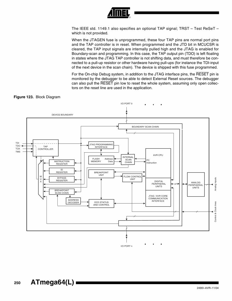
The IEEE std. 1149.1 also specifies an optional TAP signal; TRST – Test ReSeT –which is not provided.
When the JTAGEN fuse is unprogrammed, these four TAP pins are normal port pinsand the TAP controller is in reset. When programmed and the JTD bit in MCUCSR iscleared, the TAP input signals are internally pulled high and the JTAG is enabled forBoundary-scan and programming. In this case, the TAP output pin (TDO) is left floatingin states where the JTAG TAP controller is not shifting data, and must therefore be con-nected to a pull-up resistor or other hardware having pull-ups (for instance the TDI-inputof the next device in the scan chain). The device is shipped with this fuse programmed.
For the On-chip Debug system, in addition to the JTAG interface pins, the RESET pin ismonitored by the debugger to be able to detect External Reset sources. The debuggercan also pull the RESET pin low to reset the whole system, assuming only open collec-tors on the reset line are used in the application.
Figure 123. Block Diagram
TAPCONTROLLER
TDITDOTCKTMS
FLASHMEMORY
AVR CPU
DIGITALPERIPHERAL
UNITS
JTAG / AVR CORECOMMUNICATION
INTERFACE
BREAKPOINTUNIT
FLOW CONTROLUNIT
OCD STATUSAND CONTROL
INTERNAL SCANCHAIN
MUX
INSTRUCTIONREGISTER
IDREGISTER
BYPASSREGISTER
JTAG PROGRAMMINGINTERFACE
PCInstruction
AddressData
BREAKPOINTSCAN CHAIN
ADDRESSDECODER
ANALOGPERIPHERIAL
UNITS
I/O PORT 0
I/O PORT n
BOUNDARY SCAN CHAIN
Analo
g in
puts
Contr
ol &
Clo
ck li
nes
DEVICE BOUNDARY
250 ATmega64(L)2490I–AVR–11/04
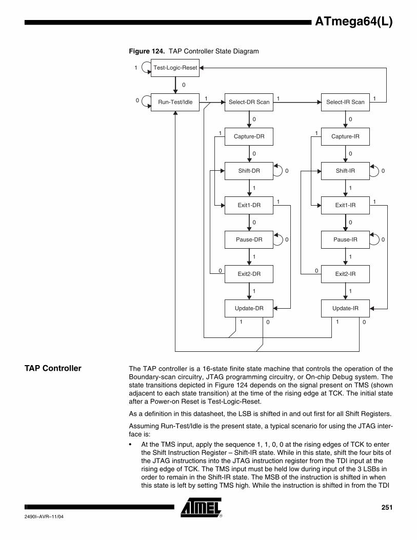
ATmega64(L)
Figure 124. TAP Controller State Diagram
TAP Controller The TAP controller is a 16-state finite state machine that controls the operation of theBoundary-scan circuitry, JTAG programming circuitry, or On-chip Debug system. Thestate transitions depicted in Figure 124 depends on the signal present on TMS (shownadjacent to each state transition) at the time of the rising edge at TCK. The initial stateafter a Power-on Reset is Test-Logic-Reset.
As a definition in this datasheet, the LSB is shifted in and out first for all Shift Registers.
Assuming Run-Test/Idle is the present state, a typical scenario for using the JTAG inter-face is:
• At the TMS input, apply the sequence 1, 1, 0, 0 at the rising edges of TCK to enter the Shift Instruction Register – Shift-IR state. While in this state, shift the four bits of the JTAG instructions into the JTAG instruction register from the TDI input at the rising edge of TCK. The TMS input must be held low during input of the 3 LSBs in order to remain in the Shift-IR state. The MSB of the instruction is shifted in when this state is left by setting TMS high. While the instruction is shifted in from the TDI
Test-Logic-Reset
Run-Test/Idle
Shift-DR
Exit1-DR
Pause-DR
Exit2-DR
Update-DR
Select-IR Scan
Capture-IR
Shift-IR
Exit1-IR
Pause-IR
Exit2-IR
Update-IR
Select-DR Scan
Capture-DR
0
1
0 1 1 1
0 0
0 0
1 1
1 0
1
1
0
1
0
0
1 0
1
1
0
1
0
0
00
11
2512490I–AVR–11/04
pin, the captured IR-state 0x01 is shifted out on the TDO pin. The JTAG Instruction selects a particular Data Register as path between TDI and TDO and controls the circuitry surrounding the selected data register.
• Apply the TMS sequence 1, 1, 0 to reenter the Run-Test/Idle state. The instruction is latched onto the parallel output from the Shift Register path in the Update-IR state. The Exit-IR, Pause-IR, and Exit2-IR states are only used for navigating the state machine.
• At the TMS input, apply the sequence 1, 0, 0 at the rising edges of TCK to enter the Shift Data Register – Shift-DR state. While in this state, upload the selected data register (selected by the present JTAG instruction in the JTAG Instruction Register) from the TDI input at the rising edge of TCK. In order to remain in the Shift-DR state, the TMS input must be held low during input of all bits except the MSB. The MSB of the data is shifted in when this state is left by setting TMS high. While the data register is shifted in from the TDI pin, the parallel inputs to the data register captured in the Capture-DR state is shifted out on the TDO pin.
• Apply the TMS sequence 1, 1, 0 to reenter the Run-Test/Idle state. If the selected data register has a latched parallel-output, the latching takes place in the Update-DR state. The Exit-DR, Pause-DR, and Exit2-DR states are only used for navigating the state machine.
As shown in the state diagram, the Run-Test/Idle state need not be entered betweenselecting JTAG instruction and using data registers, and some JTAG instructions mayselect certain functions to be performed in the Run-Test/Idle, making it unsuitable as anIdle state.Note: Independent of the initial state of the TAP Controller, the Test-Logic-Reset state can
always be entered by holding TMS high for five TCK clock periods.
For detailed information on the JTAG specification, refer to the literature listed in “Bibli-ography” on page 254.
Using the Boundary -scan Chain
A complete description of the Boundary-scan capabilities are given in the section “IEEE1149.1 (JTAG) Boundary-scan” on page 255.
Using the On-chip Debug system
As shown in Figure 123, the hardware support for On-chip Debugging consists mainlyof:
• A scan chain on the interface between the internal AVR CPU and the internal peripheral units.
• Break Point unit.
• Communication interface between the CPU and JTAG system.
All read or modify/write operations needed for implementing the Debugger are done byapplying AVR instructions via the internal AVR CPU Scan Chain. The CPU sends theresult to an I/O memory mapped location which is part of the communication interfacebetween the CPU and the JTAG system.
The Break Point Unit implements Break on Change of Program Flow, Single StepBreak, two Program Memory Break Points, and two combined Break Points. Together,the four Break Points can be configured as either:
• 4 Single Program Memory Break Points.
• 3 Single Program Memory Break Points + 1 Single Data Memory Break Point.
• 2 Single Program Memory Break Points + 2 Single Data Memory Break Points.
252 ATmega64(L)2490I–AVR–11/04
ATmega64(L)
• 2 Single Program Memory Break Points + 1 Program Memory Break Point with mask (“range Break Point”).
• 2 Single Program Memory Break Points + 1 Data Memory Break Point with mask (“range Break Point”).
A debugger, like the AVR Studio®, may however use one or more of these resources forits internal purpose, leaving less flexibility to the end-user.
A list of the On-chip Debug specific JTAG instructions is given in “On-chip Debug Spe-cific JTAG Instructions” on page 253.
The JTAGEN Fuse must be programmed to enable the JTAG Test Access Port. In addi-tion, the OCDEN Fuse must be programmed and no Lock bits must be set for the On-chip Debug system to work. As a security feature, the On-chip Debug system is disabledwhen any Lock bits are set. Otherwise, the On-chip Debug system would have provideda back-door into a secured device.
The AVR Studio enables the user to fully control execution of programs on an AVRdevice with On-chip Debug capability, AVR In-Circuit Emulator, or the built-in AVRInstruction Set Simulator. AVR Studio supports source level execution of Assembly pro-grams assembled with Atmel AVR Assembler and C programs compiled with third partyvendors’ compilers.
AVR Studio runs under Microsoft® Windows® 95/98/2000/XP/NT®.
For a full description of the AVR Studio, please refer to the AVR Studio User Guide.Only highlights are presented in this document.
All necessary execution commands are available in AVR Studio, both on source leveland on disassembly level. The user can execute the program, single step through thecode either by tracing into or stepping over functions, step out of functions, place thecursor on a statement and execute until the statement is reached, stop the execution,and reset the execution target. In addition, the user can have an unlimited number ofcode Break Points (using the BREAK instruction) and up to two data memory BreakPoints, alternatively combined as a mask (range) Break Point.
On-chip Debug Specific JTAG Instructions
The On-chip debug support is considered being private JTAG instructions, and distrib-uted within ATMEL and to selected third party vendors only. Instruction opcodes arelisted for reference.
PRIVATE0; 0x8 Private JTAG instruction for accessing On-chip Debug system.
PRIVATE1; 0x9 Private JTAG instruction for accessing On-chip Debug system.
PRIVATE2; 0xA Private JTAG instruction for accessing On-chip Debug system.
PRIVATE3; 0xB Private JTAG instruction for accessing On-chip Debug system.
2532490I–AVR–11/04
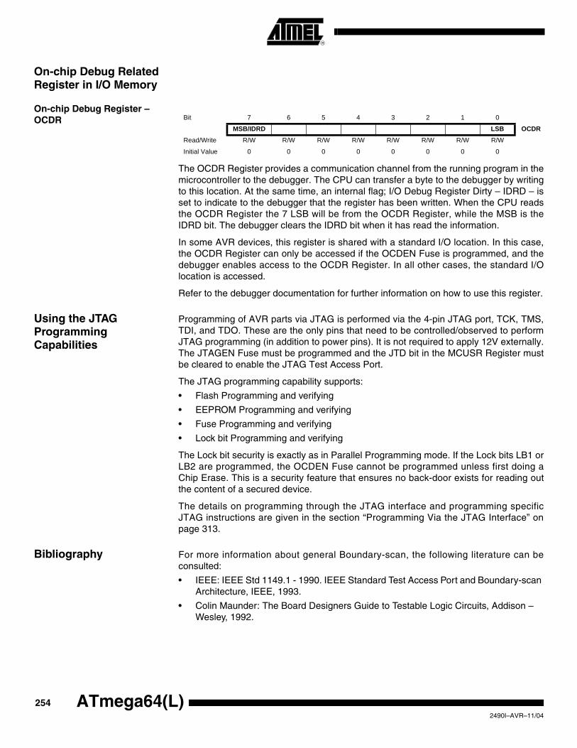
On-chip Debug Related Register in I/O Memory
On-chip Debug Register – OCDR
The OCDR Register provides a communication channel from the running program in themicrocontroller to the debugger. The CPU can transfer a byte to the debugger by writingto this location. At the same time, an internal flag; I/O Debug Register Dirty – IDRD – isset to indicate to the debugger that the register has been written. When the CPU readsthe OCDR Register the 7 LSB will be from the OCDR Register, while the MSB is theIDRD bit. The debugger clears the IDRD bit when it has read the information.
In some AVR devices, this register is shared with a standard I/O location. In this case,the OCDR Register can only be accessed if the OCDEN Fuse is programmed, and thedebugger enables access to the OCDR Register. In all other cases, the standard I/Olocation is accessed.
Refer to the debugger documentation for further information on how to use this register.
Using the JTAG Programming Capabilities
Programming of AVR parts via JTAG is performed via the 4-pin JTAG port, TCK, TMS,TDI, and TDO. These are the only pins that need to be controlled/observed to performJTAG programming (in addition to power pins). It is not required to apply 12V externally.The JTAGEN Fuse must be programmed and the JTD bit in the MCUSR Register mustbe cleared to enable the JTAG Test Access Port.
The JTAG programming capability supports:
• Flash Programming and verifying
• EEPROM Programming and verifying
• Fuse Programming and verifying
• Lock bit Programming and verifying
The Lock bit security is exactly as in Parallel Programming mode. If the Lock bits LB1 orLB2 are programmed, the OCDEN Fuse cannot be programmed unless first doing aChip Erase. This is a security feature that ensures no back-door exists for reading outthe content of a secured device.
The details on programming through the JTAG interface and programming specificJTAG instructions are given in the section “Programming Via the JTAG Interface” onpage 313.
Bibliography For more information about general Boundary-scan, the following literature can beconsulted:
• IEEE: IEEE Std 1149.1 - 1990. IEEE Standard Test Access Port and Boundary-scan Architecture, IEEE, 1993.
• Colin Maunder: The Board Designers Guide to Testable Logic Circuits, Addison –Wesley, 1992.
Bit 7 6 5 4 3 2 1 0
MSB/IDRD LSB OCDRRead/Write R/W R/W R/W R/W R/W R/W R/W R/W
Initial Value 0 0 0 0 0 0 0 0
254 ATmega64(L)2490I–AVR–11/04
ATmega64(L)
IEEE 1149.1 (JTAG) Boundary-scan
Features • JTAG (IEEE std. 1149.1 Compliant) Interface• Boundary-scan Capabilities According to the JTAG Standard• Full Scan of all Port Functions as well as Analog Circuitry Having Off-chip Connections• Supports the Optional IDCODE Instruction• Additional Public AVR_RESET Instruction to Reset the AVR
System Overview The Boundary-scan chain has the capability of driving and observing the logic levels onthe digital I/O pins, as well as the boundary between digital and analog logic for analogcircuitry having Off-chip connections. At system level, all ICs having JTAG capabilitiesare connected serially by the TDI/TDO signals to form a long Shift Register. An externalcontroller sets up the devices to drive values at their output pins, and observe the inputvalues received from other devices. The controller compares the received data with theexpected result. In this way, Boundary-scan provides a mechanism for testing intercon-nections and integrity of components on Printed Circuits Boards by using the four TAPsignals only.
The four IEEE 1149.1 defined mandatory JTAG instructions IDCODE, BYPASS, SAM-PLE/PRELOAD, and EXTEST, as well as the AVR specific public JTAG instructionAVR_RESET can be used for testing the printed circuit board. Initial scanning of thedata register path will show the ID-Code of the device, since IDCODE is the defaultJTAG instruction. It may be desirable to have the AVR device in reset during test mode.If not reset, inputs to the device may be determined by the scan operations, and theinternal software may be in an undetermined state when exiting the test mode. Enteringreset, the outputs of any Port Pin will instantly enter the high impedance state, makingthe HIGHZ instruction redundant. If needed, the BYPASS instruction can be issued tomake the shortest possible scan chain through the device. The device can be set in thereset state either by pulling the external RESET pin low, or issuing the AVR_RESETinstruction with appropriate setting of the Reset Data Register.
The EXTEST instruction is used for sampling external pins and loading output pins withdata. The data from the output latch will be driven out on the pins as soon as theEXTEST instruction is loaded into the JTAG IR-Register. Therefore, the SAMPLE/PRE-LOAD should also be used for setting initial values to the scan ring, to avoid damagingthe board when issuing the EXTEST instruction for the first time. SAMPLE/PRELOADcan also be used for taking a snapshot of the external pins during normal operation ofthe part.
The JTAGEN Fuse must be programmed and the JTD bit in the I/O Register MCUCSRmust be cleared to enable the JTAG Test Access Port.
When using the JTAG interface for Boundary-scan, using a JTAG TCK clock frequencyhigher than the internal chip frequency is possible. The chip clock is not required to run.
Data Registers The data registers relevant for Boundary-scan operations are:
• Bypass Register
• Device Identification Register
• Reset Register
• Boundary-scan Chain
2552490I–AVR–11/04
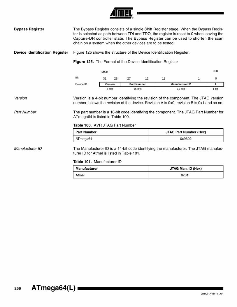
Bypass Register The Bypass Register consists of a single Shift Register stage. When the Bypass Regis-ter is selected as path between TDI and TDO, the register is reset to 0 when leaving theCapture-DR controller state. The Bypass Register can be used to shorten the scanchain on a system when the other devices are to be tested.
Device Identification Register Figure 125 shows the structure of the Device Identification Register.
Figure 125. The Format of the Device Identification Register
Version Version is a 4-bit number identifying the revision of the component. The JTAG versionnumber follows the revision of the device. Revision A is 0x0, revision B is 0x1 and so on.
Part Number The part number is a 16-bit code identifying the component. The JTAG Part Number forATmega64 is listed in Table 100.
Manufacturer ID The Manufacturer ID is a 11-bit code identifying the manufacturer. The JTAG manufac-turer ID for Atmel is listed in Table 101.
MSB LSB
Bit 31 28 27 12 11 1 0
Device ID Version Part Number Manufacturer ID 14 bits 16 bits 11 bits 1-bit
Table 100. AVR JTAG Part Number
Part Number JTAG Part Number (Hex)
ATmega64 0x9602
Table 101. Manufacturer ID
Manufacturer JTAG Man. ID (Hex)
Atmel 0x01F
256 ATmega64(L)2490I–AVR–11/04
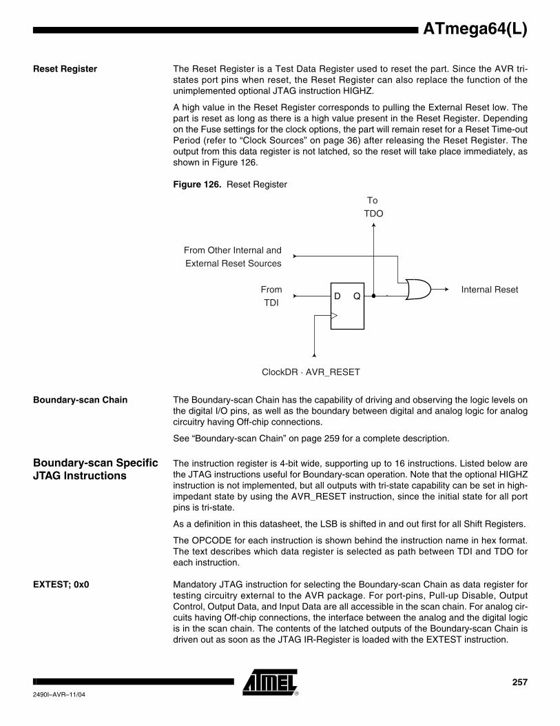
ATmega64(L)
Reset Register The Reset Register is a Test Data Register used to reset the part. Since the AVR tri-states port pins when reset, the Reset Register can also replace the function of theunimplemented optional JTAG instruction HIGHZ.
A high value in the Reset Register corresponds to pulling the External Reset low. Thepart is reset as long as there is a high value present in the Reset Register. Dependingon the Fuse settings for the clock options, the part will remain reset for a Reset Time-outPeriod (refer to “Clock Sources” on page 36) after releasing the Reset Register. Theoutput from this data register is not latched, so the reset will take place immediately, asshown in Figure 126.
Figure 126. Reset Register
Boundary-scan Chain The Boundary-scan Chain has the capability of driving and observing the logic levels onthe digital I/O pins, as well as the boundary between digital and analog logic for analogcircuitry having Off-chip connections.
See “Boundary-scan Chain” on page 259 for a complete description.
Boundary-scan Specific JTAG Instructions
The instruction register is 4-bit wide, supporting up to 16 instructions. Listed below arethe JTAG instructions useful for Boundary-scan operation. Note that the optional HIGHZinstruction is not implemented, but all outputs with tri-state capability can be set in high-impedant state by using the AVR_RESET instruction, since the initial state for all portpins is tri-state.
As a definition in this datasheet, the LSB is shifted in and out first for all Shift Registers.
The OPCODE for each instruction is shown behind the instruction name in hex format.The text describes which data register is selected as path between TDI and TDO foreach instruction.
EXTEST; 0x0 Mandatory JTAG instruction for selecting the Boundary-scan Chain as data register fortesting circuitry external to the AVR package. For port-pins, Pull-up Disable, OutputControl, Output Data, and Input Data are all accessible in the scan chain. For analog cir-cuits having Off-chip connections, the interface between the analog and the digital logicis in the scan chain. The contents of the latched outputs of the Boundary-scan Chain isdriven out as soon as the JTAG IR-Register is loaded with the EXTEST instruction.
D QFromTDI
ClockDR · AVR_RESET
To TDO
From Other Internal andExternal Reset Sources
Internal Reset
2572490I–AVR–11/04
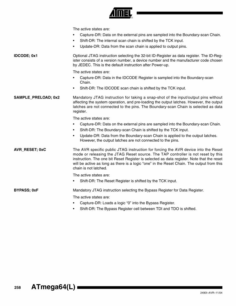
The active states are:
• Capture-DR: Data on the external pins are sampled into the Boundary-scan Chain.
• Shift-DR: The internal scan chain is shifted by the TCK input.
• Update-DR: Data from the scan chain is applied to output pins.
IDCODE; 0x1 Optional JTAG instruction selecting the 32-bit ID-Register as data register. The ID-Reg-ister consists of a version number, a device number and the manufacturer code chosenby JEDEC. This is the default instruction after Power-up.
The active states are:
• Capture-DR: Data in the IDCODE Register is sampled into the Boundary-scan Chain.
• Shift-DR: The IDCODE scan chain is shifted by the TCK input.
SAMPLE_PRELOAD; 0x2 Mandatory JTAG instruction for taking a snap-shot of the input/output pins withoutaffecting the system operation, and pre-loading the output latches. However, the outputlatches are not connected to the pins. The Boundary-scan Chain is selected as dataregister.
The active states are:
• Capture-DR: Data on the external pins are sampled into the Boundary-scan Chain.
• Shift-DR: The Boundary-scan Chain is shifted by the TCK input.
• Update-DR: Data from the Boundary-scan Chain is applied to the output latches. However, the output latches are not connected to the pins.
AVR_RESET; 0xC The AVR specific public JTAG instruction for forcing the AVR device into the Resetmode or releasing the JTAG Reset source. The TAP controller is not reset by thisinstruction. The one bit Reset Register is selected as data register. Note that the resetwill be active as long as there is a logic “one” in the Reset Chain. The output from thischain is not latched.
The active states are:
• Shift-DR: The Reset Register is shifted by the TCK input.
BYPASS; 0xF Mandatory JTAG instruction selecting the Bypass Register for Data Register.
The active states are:
• Capture-DR: Loads a logic “0” into the Bypass Register.
• Shift-DR: The Bypass Register cell between TDI and TDO is shifted.
258 ATmega64(L)2490I–AVR–11/04
ATmega64(L)
Boundary-scan Related Register in I/O Memory
MCU Control and Status Register – MCUCSR
The MCU Control and Status Register contains control bits for general MCU functions,and provides information on which reset source caused an MCU Reset.
• Bit 7 – JTD: JTAG Interface Disable
When this bit is zero, the JTAG interface is enabled if the JTAGEN Fuse is programmed.If this bit is one, the JTAG interface is disabled. In order to avoid unintentional disablingor enabling of the JTAG interface, a timed sequence must be followed when changingthis bit: The application software must write this bit to the desired value twice within fourcycles to change its value.
If the JTAG interface is left unconnected to other JTAG circuitry, the JTD bit should beset to one. The reason for this is to avoid static current at the TDO pin in the JTAGinterface.
• Bit 4 – JTRF: JTAG Reset Flag
This bit is set if a reset is being caused by a logic one in the JTAG Reset Registerselected by the JTAG instruction AVR_RESET. This bit is reset by a Brown-out Reset,or by writing a logic zero to the flag.
Boundary-scan Chain The Boundary-scan Chain has the capability of driving and observing the logic levels onthe digital I/O pins, as well as the boundary between digital and analog logic for analogcircuitry having Off-chip connection.
Scanning the Digital Port Pins Figure 127 shows the Boundary-scan Cell for a bi-directional port pin with pull-up func-tion. The cell consists of a standard Boundary-scan cell for the Pull-up Enable – PUExn– function, and a bi-directional pin cell that combines the three signals, Output Control –OCxn, Output Data – ODxn, and Input Data – IDxn, into only a two-stage Shift Register.The port and pin indexes are not used in the following description.
The Boundary-scan logic is not included in the figures in this Datasheet. Figure 128shows a simple digital Port Pin as described in the section “I/O Ports” on page 65. TheBoundary-scan details from Figure 127 replaces the dashed box in Figure 128.
When no alternate port function is present, the Input Data – ID corresponds to the PINxnRegister value (but ID has no synchronizer), Output Data corresponds to the PORTRegister, Output Control corresponds to the Data Direction – DD Register, and the Pull-up Enable – PUExn – corresponds to logic expression PUD · DDxn · PORTxn.
Digital alternate port functions are connected outside the dotted box in Figure 128 tomake the scan chain read the actual pin value. For analog function, there is a direct con-nection from the external pin to the analog circuit, and a scan chain is inserted on theinterface between the digital logic and the analog circuitry.
Bit 7 6 5 4 3 2 1 0
JTD – – JTRF WDRF BORF EXTRF PORF MCUCSRRead/Write R/W R R R/W R/W R/W R/W R/W
Initial Value 0 0 0 See Bit Description
2592490I–AVR–11/04
Figure 127. Boundary-scan Cell for Bi-directional Port Pin with Pull-up Function
D Q D Q
G
0
10
1
D Q D Q
G
0
10
1
0
1
0
1D Q D Q
G
0
1
Por
t Pin
(P
Xn)
VccEXTESTTo Next CellShiftDR
Out
put C
ontr
ol (
OC
)P
ullu
p E
nabl
e (P
UE
)O
utpu
t Dat
a (O
D)
Inpu
t Dat
a (I
D)
From Last Cell UpdateDRClockDR
FF2 LD2
FF1 LD1
LD0FF0
260 ATmega64(L)2490I–AVR–11/04
ATmega64(L)
Figure 128. General Port Pin Schematic Diagram
Boundary-scan and the Two-wire Interface
The two Two-wire Interface pins SCL and SDA have one additional control signal in thescan-chain; Two-wire Interface Enable – TWIEN. As shown in Figure 129, the TWIENsignal enables a tri-state buffer with slew-rate control in parallel with the ordinary digitalport pins. A general scan cell as shown in Figure 133 is attached to the TWIEN signal.Notes: 1. A separate scan chain for the 50 ns spike filter on the input is not provided. The ordi-
nary scan support for digital port pins suffice for connectivity tests. The only reasonfor having TWIEN in the scan path, is to be able to disconnect the slew-rate controlbuffer when doing boundary-scan.
2. Make sure the OC and TWIEN signals are not asserted simultaneously, as this willlead to drive contention.
CLK
RPx
RRx
WPx
RDx
WDx
PUD
SYNCHRONIZER
WDx: WRITE DDRx
WPx: WRITE PORTxRRx: READ PORTx REGISTERRPx: READ PORTx PIN
PUD: PULLUP DISABLE
CLK : I/O CLOCK
RDx: READ DDRx
D
L
Q
Q
RESET
RESET
Q
QD
Q
Q D
CLR
PORTxn
Q
Q D
CLR
DDxn
PINxn
DAT
A B
US
SLEEP
SLEEP: SLEEP CONTROL
Pxn
I/O
I/O
See Boundary-scan Descriptionfor Details!
PUExn
OCxn
ODxn
IDxn
PUExn: PULLUP ENABLE for pin PxnOCxn: OUTPUT CONTROL for pin PxnODxn: OUTPUT DATA to pin PxnIDxn: INPUT DATA from pin Pxn
2612490I–AVR–11/04
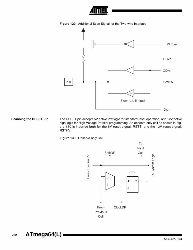
Figure 129. Additional Scan Signal for the Two-wire Interface
Scanning the RESET Pin The RESET pin accepts 5V active low logic for standard reset operation, and 12V activehigh logic for High Voltage Parallel programming. An observe-only cell as shown in Fig-ure 130 is inserted both for the 5V reset signal; RSTT, and the 12V reset signal;RSTHV.
Figure 130. Observe-only Cell
Pxn
PUExn
ODxn
IDxn
TWIEN
OCxn
Slew-rate limited
SRC
0
1D Q
FromPrevious
Cell
ClockDR
ShiftDR
ToNextCell
Fro
m S
yste
m P
in
To
Sys
tem
Log
ic
FF1
262 ATmega64(L)2490I–AVR–11/04
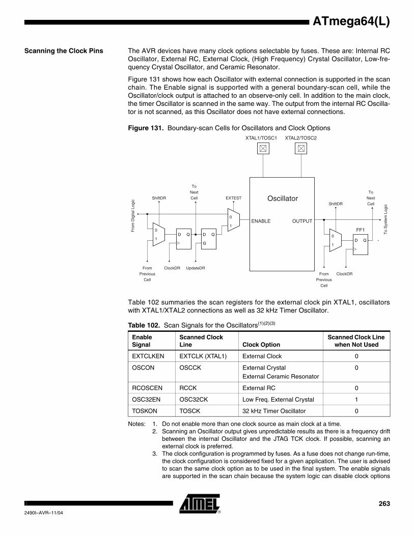
ATmega64(L)
Scanning the Clock Pins The AVR devices have many clock options selectable by fuses. These are: Internal RCOscillator, External RC, External Clock, (High Frequency) Crystal Oscillator, Low-fre-quency Crystal Oscillator, and Ceramic Resonator.
Figure 131 shows how each Oscillator with external connection is supported in the scanchain. The Enable signal is supported with a general boundary-scan cell, while theOscillator/clock output is attached to an observe-only cell. In addition to the main clock,the timer Oscillator is scanned in the same way. The output from the internal RC Oscilla-tor is not scanned, as this Oscillator does not have external connections.
Figure 131. Boundary-scan Cells for Oscillators and Clock Options
Table 102 summaries the scan registers for the external clock pin XTAL1, oscillatorswith XTAL1/XTAL2 connections as well as 32 kHz Timer Oscillator.
Notes: 1. Do not enable more than one clock source as main clock at a time.2. Scanning an Oscillator output gives unpredictable results as there is a frequency drift
between the internal Oscillator and the JTAG TCK clock. If possible, scanning anexternal clock is preferred.
3. The clock configuration is programmed by fuses. As a fuse does not change run-time,the clock configuration is considered fixed for a given application. The user is advisedto scan the same clock option as to be used in the final system. The enable signalsare supported in the scan chain because the system logic can disable clock options
Table 102. Scan Signals for the Oscillators(1)(2)(3)
Enable Signal
Scanned Clock Line Clock Option
Scanned Clock Line when Not Used
EXTCLKEN EXTCLK (XTAL1) External Clock 0
OSCON OSCCK External CrystalExternal Ceramic Resonator
0
RCOSCEN RCCK External RC 0
OSC32EN OSC32CK Low Freq. External Crystal 1
TOSKON TOSCK 32 kHz Timer Oscillator 0
0
1D Q
FromPrevious
Cell
ClockDR
ShiftDR
ToNextCell
To
Sys
tem
Log
ic
FF10
1D Q D Q
G
0
1
FromPrevious
Cell
ClockDR UpdateDR
ShiftDR
ToNextCell EXTEST
Fro
m D
igita
l Log
icXTAL1/TOSC1 XTAL2/TOSC2
Oscillator
ENABLE OUTPUT
2632490I–AVR–11/04
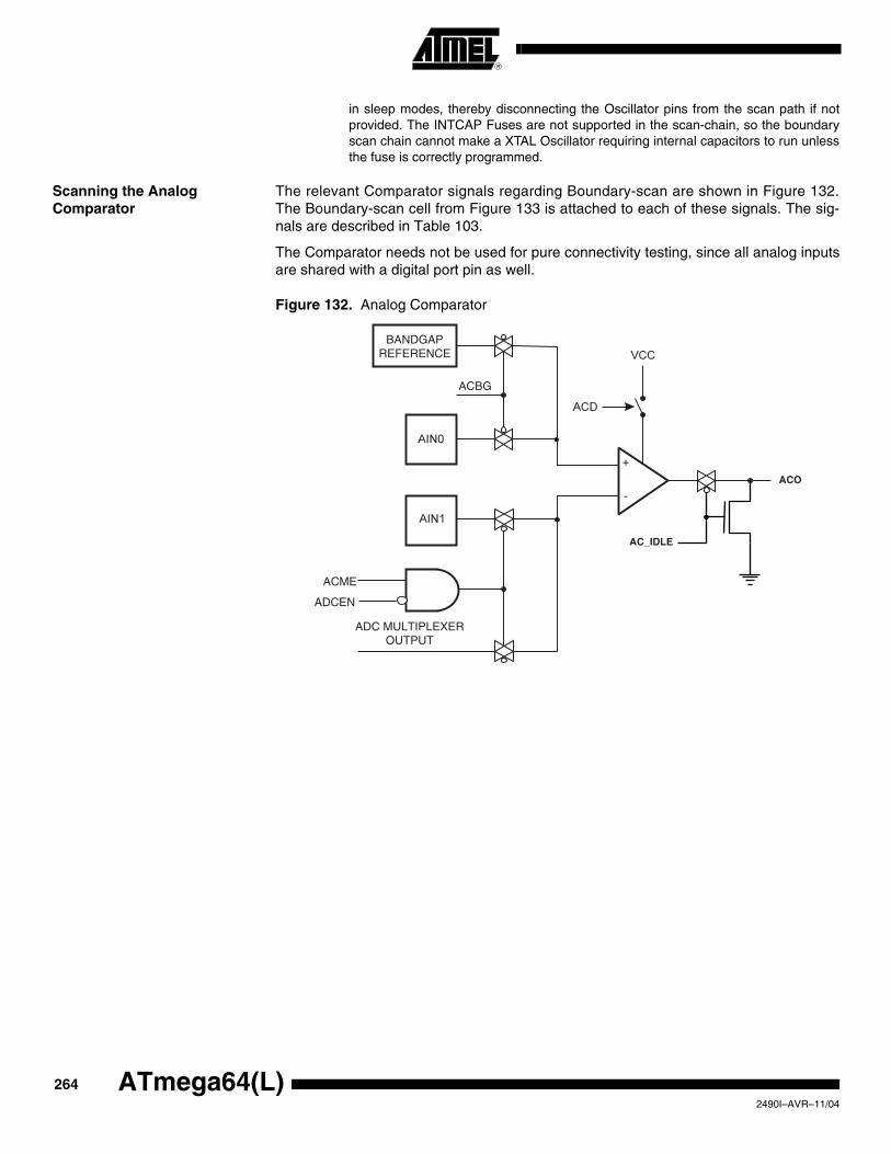
in sleep modes, thereby disconnecting the Oscillator pins from the scan path if notprovided. The INTCAP Fuses are not supported in the scan-chain, so the boundaryscan chain cannot make a XTAL Oscillator requiring internal capacitors to run unlessthe fuse is correctly programmed.
Scanning the Analog Comparator
The relevant Comparator signals regarding Boundary-scan are shown in Figure 132.The Boundary-scan cell from Figure 133 is attached to each of these signals. The sig-nals are described in Table 103.
The Comparator needs not be used for pure connectivity testing, since all analog inputsare shared with a digital port pin as well.
Figure 132. Analog Comparator
ACBG
BANDGAPREFERENCE
ADC MULTIPLEXEROUTPUT
ACME
AC_IDLE
ACO
ADCEN
264 ATmega64(L)2490I–AVR–11/04
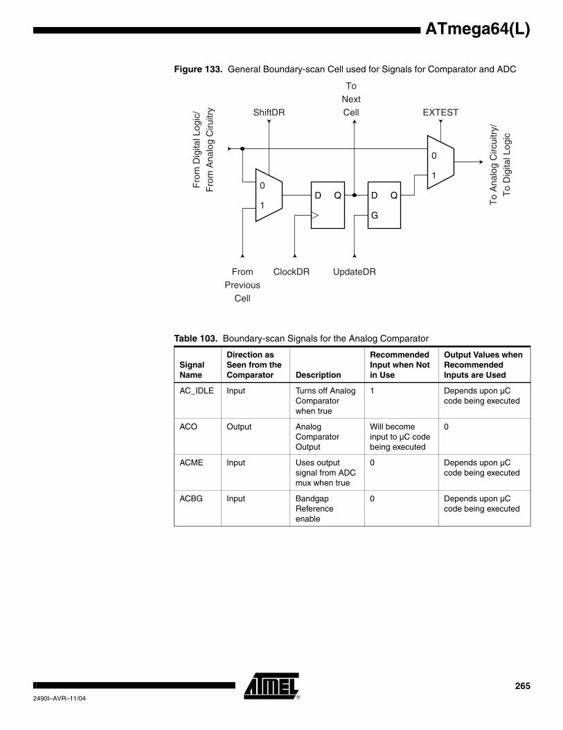
ATmega64(L)
Figure 133. General Boundary-scan Cell used for Signals for Comparator and ADC
Table 103. Boundary-scan Signals for the Analog Comparator
Signal Name
Direction as Seen from the Comparator Description
Recommended Input when Not in Use
Output Values when Recommended Inputs are Used
AC_IDLE Input Turns off Analog Comparator when true
1 Depends upon µC code being executed
ACO Output Analog Comparator Output
Will become input to µC code being executed
0
ACME Input Uses output signal from ADC mux when true
0 Depends upon µC code being executed
ACBG Input Bandgap Reference enable
0 Depends upon µC code being executed
0
1D Q D Q
G
0
1
FromPrevious
Cell
ClockDR UpdateDR
ShiftDR
ToNextCell EXTEST
To
Ana
log
Circ
uitr
y/T
o D
igita
l Log
ic
Fro
m D
igita
l Log
ic/
Fro
m A
nalo
g C
iruitr
y
2652490I–AVR–11/04
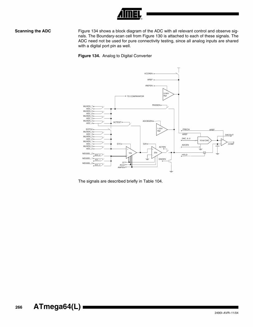
Scanning the ADC Figure 134 shows a block diagram of the ADC with all relevant control and observe sig-nals. The Boundary-scan cell from Figure 130 is attached to each of these signals. TheADC need not be used for pure connectivity testing, since all analog inputs are sharedwith a digital port pin as well.
Figure 134. Analog to Digital Converter
The signals are described briefly in Table 104.
10-bit DAC +
-
AREF
PRECH
DACOUT
MUXEN_7ADC_7
MUXEN_6ADC_6
MUXEN_5ADC_5
MUXEN_4ADC_4
MUXEN_3ADC_3
MUXEN_2ADC_2
MUXEN_1ADC_1
MUXEN_0ADC_0
NEGSEL_2ADC_2
NEGSEL_1ADC_1
NEGSEL_0ADC_0
EXTCH
+
-
+
-10x 20x
G10 G20
STACLK
AMPEN
2.56VRef
IREFEN
AREF
VCCREN
DAC_9..0
ADCEN
HOLD
GNDEN
PASSEN
ACTEN
COMP
SCTESTADCBGEN
TO COMPARATOR
1.22VRef AREF
266 ATmega64(L)2490I–AVR–11/04
ATmega64(L)
Table 104. Boundary-scan Signals for the ADC(1)
Signal Name
Direction as Seen from the ADC Description
Recommended Input when not
in Use
Output Values when Recommended Inputs are Used, and CPU is
not Using the ADC
COMP Output Comparator Output 0 0
ACLK Input Clock signal to gain stages implemented as Switch-cap filters
0 0
ACTEN Input Enable path from gain stages to the Comparator
0 0
ADCBGEN Input Enable Band-gap reference as negative input to Comparator
0 0
ADCEN Input Power-on signal to the ADC
0 0
AMPEN Input Power-on signal to the gain stages
0 0
DAC_9 Input Bit nine of digital value to DAC
1 1
DAC_8 Input Bit eight of digital value to DAC
0 0
DAC_7 Input Bit seven of digital value to DAC
0 0
DAC_6 Input Bit six of digital value to DAC
0 0
DAC_5 Input Bit five of digital value to DAC
0 0
DAC_4 Input Bit four of digital value to DAC
0 0
DAC_3 Input Bit three of digital value to DAC
0 0
DAC_2 Input Bit two of digital value to DAC
0 0
DAC_1 Input Bit 1 of digital value to DAC
0 0
DAC_0 Input Bit 0 of digital value to DAC
0 0
EXTCH Input Connect ADC channels 0 - 3 to bypass path around gain stages
1 1
G10 Input Enable 10x gain 0 0
G20 Input Enable 20x gain 0 0
2672490I–AVR–11/04
GNDEN Input Ground the negative input to comparator when true
0 0
HOLD Input Sample&Hold signal. Sample analog signal when low. Hold signal when high. If gain stages are used, this signal must go active when ACLK is high.
1 1
IREFEN Input Enables Band-gap reference as AREF signal to DAC
0 0
MUXEN_7 Input Input Mux bit 7 0 0
MUXEN_6 Input Input Mux bit 6 0 0
MUXEN_5 Input Input Mux bit 5 0 0
MUXEN_4 Input Input Mux bit 4 0 0
MUXEN_3 Input Input Mux bit 3 0 0
MUXEN_2 Input Input Mux bit 2 0 0
MUXEN_1 Input Input Mux bit 1 0 0
MUXEN_0 Input Input Mux bit 0 1 1
NEGSEL_2 Input Input Mux for negative input for differential signal, bit 2
0 0
NEGSEL_1 Input Input Mux for negative input for differential signal, bit 1
0 0
NEGSEL_0 Input Input Mux for negative input for differential signal, bit 0
0 0
PASSEN Input Enable pass-gate of gain stages.
1 1
PRECH Input Precharge output latch of comparator (Active low)
1 1
Table 104. Boundary-scan Signals for the ADC(1) (Continued)
Signal Name
Direction as Seen from the ADC Description
Recommended Input when not
in Use
Output Values when Recommended Inputs are Used, and CPU is
not Using the ADC
268 ATmega64(L)2490I–AVR–11/04
ATmega64(L)
Note: 1. Incorrect setting of the switches in Figure 134 will make signal contention and maydamage the part. There are several input choices to the S&H circuitry on the negativeinput of the output comparator in Figure 134. Make sure only one path is selectedfrom either one ADC pin, Bandgap reference source, or Ground.
If the ADC is not to be used during scan, the recommended input values from Table 104should be used. The user is recommended not to use the Differential Gain stages dur-ing scan. Switch-cap based gain stages require fast operation and accurate timingwhich is difficult to obtain when used in a scan chain. Details concerning operations ofthe differential gain stage is therefore not provided.
The AVR ADC is based on the analog circuitry shown in Figure 134 with a successiveapproximation algorithm implemented in the digital logic. When used in Boundary-scan,the problem is usually to ensure that an applied analog voltage is measured within somelimits. This can easily be done without running a successive approximation algorithm:apply the lower limit on the digital DAC[9:0] lines, make sure the output from the com-parator is low, then apply the upper limit on the digital DAC[9:0] lines, and verify theoutput from the comparator to be high.
The ADC needs not be used for pure connectivity testing, since all analog inputs areshared with a digital port pin as well.
When using the ADC, remember the following:
• The Port Pin for the ADC channel in use must be configured to be an input with pull-up disabled to avoid signal contention.
• In Normal mode, a dummy conversion (consisting of 10 comparisons) is performed when enabling the ADC. The user is advised to wait at least 200 ns after enabling the ADC before controlling/observing any ADC signal, or perform a dummy conversion before using the first result.
• The DAC values must be stable at the midpoint value 0x200 when having the HOLD signal low (Sample mode).
SCTEST Input Switch-cap TEST enable. Output from x10 gain stage send out to Port Pin having ADC_4
0 0
ST Input Output of gain stages will settle faster if this signal is high first two ACLK periods after AMPEN goes high.
0 0
VCCREN Input Selects Vcc as the ACC reference voltage.
0 0
Table 104. Boundary-scan Signals for the ADC(1) (Continued)
Signal Name
Direction as Seen from the ADC Description
Recommended Input when not
in Use
Output Values when Recommended Inputs are Used, and CPU is
not Using the ADC
2692490I–AVR–11/04
As an example, consider the task of verifying a 1.5V ± 5% input signal at ADC channel 3when the power supply is 5.0V and AREF is externally connected to VCC.
The recommended values from Table 104 are used unless other values are given in thealgorithm in Table 105. Only the DAC and Port Pin values of the Scan-chain are shown.The column “Actions” describes what JTAG instruction to be used before filling theBoundary-scan Register with the succeeding columns. The verification should be doneon the data scanned out when scanning in the data on the same row in the table.
Note: 1. Using this algorithm, the timing constraint on the HOLD signal constrains the TCK clock frequency. As the algorithm keepsHOLD high for five steps, the TCK clock frequency has to be at least five times the number of scan bits divided by the maxi-mum hold time, thold,max.
The lower limit is: 1024 1.5V 0,95 5V⁄⋅ ⋅ 291 0x123= = The upper limit is: 1024 1.5V 1.05 5V⁄⋅ ⋅ 323 0x143= =
Table 105. Algorithm for Using the ADC(1)
Step Actions ADCEN DAC MUXEN HOLD PRECH
PA3.Data
PA3.Control
PA3.Pull-up_
Enable
1 SAMPLE_PRELOAD 1 0x200 0x08 1 1 0 0 0
2 EXTEST 1 0x200 0x08 0 1 0 0 0
3 1 0x200 0x08 1 1 0 0 0
4 1 0x123 0x08 1 1 0 0 0
5 1 0x123 0x08 1 0 0 0 0
6 Verify the COMP bit scanned out to be 0 1 0x200 0x08 1 1 0 0 0
7 1 0x200 0x08 0 1 0 0 0
8 1 0x200 0x08 1 1 0 0 0
9 1 0x143 0x08 1 1 0 0 0
10 1 0x143 0x08 1 0 0 0 0
11 Verify the COMP bit scanned out to be 1 1 0x200 0x08 1 1 0 0 0
270 ATmega64(L)2490I–AVR–11/04
ATmega64(L)
ATmega64 Boundary-scan Order
Table 106 shows the Scan order between TDI and TDO when the Boundary-scan Chainis selected as data path. Bit 0 is the LSB; the first bit scanned in, and the first bitscanned out. The scan order follows the pinout order as far as possible. Therefore, thebits of Port A are scanned in the opposite bit order of the other ports. Exceptions fromthe rules are the scan chains for the analog circuits, which constitute the most significantbits of the scan chain regardless of which physical pin they are connected to. In Figure127, PXn, Data corresponds to FF0, PXn. Control corresponds to FF1, and PXn.Pullup_enable corresponds to FF2. Bit 2, 3, 4, and 5 of Port C is not in the scan chain,since these pins constitute the TAP pins when the JTAG is enabled.
Table 106. ATmega64 Boundary-scan Order
Bit Number Signal Name Module
204 AC_IDLE Comparator
203 ACO
202 ACME
201 AINBG
200 COMP ADC
199 PRIVATE_SIGNAL1(1)
198 ACLK
197 ACTEN
196 PRIVATE_SIGNAL2(2)
195 ADCBGEN
194 ADCEN
193 AMPEN
192 DAC_9
191 DAC_8
190 DAC_7
189 DAC_6
188 DAC_5
187 DAC_4
186 DAC_3
185 DAC_2
184 DAC_1
183 DAC_0
182 EXTCH
181 G10
180 G20
179 GNDEN
178 HOLD
177 IREFEN
176 MUXEN_7
2712490I–AVR–11/04
175 MUXEN_6 ADC
174 MUXEN_5
173 MUXEN_4
172 MUXEN_3
171 MUXEN_2
170 MUXEN_1
169 MUXEN_0
168 NEGSEL_2
167 NEGSEL_1
166 NEGSEL_0
165 PASSEN
164 PRECH
163 SCTEST
162 ST
161 VCCREN
160 PEN Programming Enable (Observe-only)
159 PE0.Data Port E
158 PE0.Control
157 PE0.Pullup_Enable
156 PE1.Data
155 PE1.Control
154 PE1.Pullup_Enable
153 PE2.Data
152 PE2.Control
151 PE2.Pullup_Enable
150 PE3.Data
149 PE3.Control
148 PE3.Pullup_Enable
147 PE4.Data
146 PE4.Control
145 PE4.Pullup_Enable
144 PE5.Data
143 PE5.Control
142 PE5.Pullup_Enable
141 PE6.Data
140 PE6.Control
Table 106. ATmega64 Boundary-scan Order (Continued)
Bit Number Signal Name Module
272 ATmega64(L)2490I–AVR–11/04
ATmega64(L)
139 PE6.Pullup_Enable Port E
138 PE7.Data
137 PE7.Control
136 PE7.Pullup_Enable
135 PB0.Data Port B
134 PB0.Control
133 PB0.Pullup_Enable
132 PB1.Data
131 PB1.Control
130 PB1.Pullup_Enable
129 PB2.Data
128 PB2.Control
127 PB2.Pullup_Enable
126 PB3.Data
125 PB3.Control
124 PB3.Pullup_Enable
123 PB4.Data
122 PB4.Control
121 PB4.Pullup_Enable
120 PB5.Data
119 PB5.Control
118 PB5.Pullup_Enable
117 PB6.Data
116 PB6.Control
115 PB6.Pullup_Enable
114 PB7.Data
113 PB7.Control
112 PB7.Pullup_Enable
111 PG3.Data Port G
110 PG3.Control
109 PG3.Pullup_Enable
108 PG4.Data
107 PG4.Control
106 PG4.Pullup_Enable
105 TOSC 32 kHz Timer Oscillator
104 TOSCON
Table 106. ATmega64 Boundary-scan Order (Continued)
Bit Number Signal Name Module
2732490I–AVR–11/04
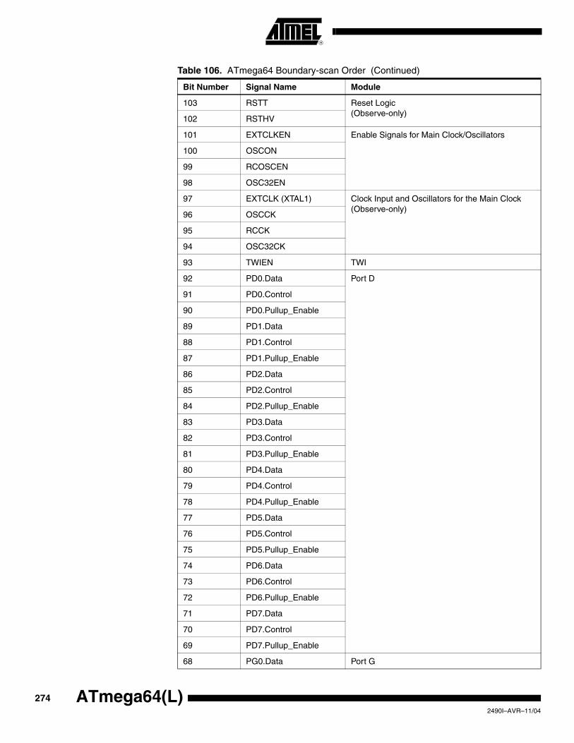
103 RSTT Reset Logic (Observe-only)
102 RSTHV
101 EXTCLKEN Enable Signals for Main Clock/Oscillators
100 OSCON
99 RCOSCEN
98 OSC32EN
97 EXTCLK (XTAL1) Clock Input and Oscillators for the Main Clock(Observe-only)
96 OSCCK
95 RCCK
94 OSC32CK
93 TWIEN TWI
92 PD0.Data Port D
91 PD0.Control
90 PD0.Pullup_Enable
89 PD1.Data
88 PD1.Control
87 PD1.Pullup_Enable
86 PD2.Data
85 PD2.Control
84 PD2.Pullup_Enable
83 PD3.Data
82 PD3.Control
81 PD3.Pullup_Enable
80 PD4.Data
79 PD4.Control
78 PD4.Pullup_Enable
77 PD5.Data
76 PD5.Control
75 PD5.Pullup_Enable
74 PD6.Data
73 PD6.Control
72 PD6.Pullup_Enable
71 PD7.Data
70 PD7.Control
69 PD7.Pullup_Enable
68 PG0.Data Port G
Table 106. ATmega64 Boundary-scan Order (Continued)
Bit Number Signal Name Module
274 ATmega64(L)2490I–AVR–11/04

ATmega64(L)
67 PG0.Control Port G
66 PG0.Pullup_Enable
65 PG1.Data
64 PG1.Control
63 PG1.Pullup_Enable
62 PC0.Data Port C
61 PC0.Control
60 PC0.Pullup_Enable
59 PC1.Data
58 PC1.Control
57 PC1.Pullup_Enable
56 PC2.Data
55 PC2.Control
54 PC2.Pullup_Enable
53 PC3.Data
52 PC3.Control
51 PC3.Pullup_Enable
50 PC4.Data
49 PC4.Control
48 PC4.Pullup_Enable
47 PC5.Data
46 PC5.Control
45 PC5.Pullup_Enable
44 PC6.Data
43 PC6.Control
42 PC6.Pullup_Enable
41 PC7.Data
40 PC7.Control
39 PC7.Pullup_Enable
38 PG2.Data Port G
37 PG2.Control
36 PG2.Pullup_Enable
35 PA7.Data Port A
34 PA7.Control
33 PA7.Pullup_Enable
32 PA6.Data
Table 106. ATmega64 Boundary-scan Order (Continued)
Bit Number Signal Name Module
2752490I–AVR–11/04
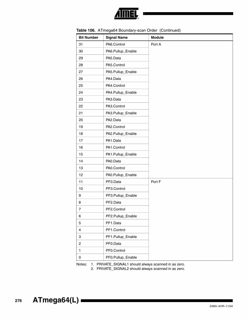
Notes: 1. PRIVATE_SIGNAL1 should always scanned in as zero.2. PRIVATE_SIGNAL2 should always scanned in as zero.
31 PA6.Control Port A
30 PA6.Pullup_Enable
29 PA5.Data
28 PA5.Control
27 PA5.Pullup_Enable
26 PA4.Data
25 PA4.Control
24 PA4.Pullup_Enable
23 PA3.Data
22 PA3.Control
21 PA3.Pullup_Enable
20 PA2.Data
19 PA2.Control
18 PA2.Pullup_Enable
17 PA1.Data
16 PA1.Control
15 PA1.Pullup_Enable
14 PA0.Data
13 PA0.Control
12 PA0.Pullup_Enable
11 PF3.Data Port F
10 PF3.Control
9 PF3.Pullup_Enable
8 PF2.Data
7 PF2.Control
6 PF2.Pullup_Enable
5 PF1.Data
4 PF1.Control
3 PF1.Pullup_Enable
2 PF0.Data
1 PF0.Control
0 PF0.Pullup_Enable
Table 106. ATmega64 Boundary-scan Order (Continued)
Bit Number Signal Name Module
276 ATmega64(L)2490I–AVR–11/04

ATmega64(L)
Boundary-scan Description Language Files
Boundary-scan Description Language (BSDL) files describe Boundary-scan capabledevices in a standard format used by automated test-generation software. The orderand function of bits in the Boundary-scan Data Register are included in this description.
2772490I–AVR–11/04

Boot Loader Support – Read-While-Write Self-programming
The Boot Loader Support provides a real Read-While-Write Self-programming mecha-nism for downloading and uploading program code by the MCU itself. This featureallows flexible application software updates controlled by the MCU using a Flash-resi-dent Boot Loader program. The Boot Loader program can use any available datainterface and associated protocol to read code and write (program) that code into theFlash memory, or read the code from the program memory. The program code withinthe Boot Loader section has the capability to write into the entire Flash, including theBoot Loader Memory. The Boot Loader can thus even modify itself, and it can alsoerase itself from the code if the feature is not needed anymore. The size of the BootLoader Memory is configurable with Fuses and the Boot Loader has two separate setsof Boot Lock bits which can be set independently. This gives the user a unique flexibilityto select different levels of protection.
Features • Read-While-Write Self-programming• Flexible Boot Memory Size• High Security (Separate Boot Lock Bits for a Flexible Protection)• Separate Fuse to Select Reset Vector• Optimized Page(1) Size• Code Efficient Algorithm• Efficient Read-Modify-Write Support
Note: 1. A page is a section in the Flash consisting of several bytes (see Table 123 on page297) used during programming. The page organization does not affect normaloperation.
Application and Boot Loader Flash Sections
The Flash memory is organized in two main sections, the Application section and theBoot Loader section (see Figure 136). The size of the different sections is configured bythe BOOTSZ Fuses as shown in Table 112 on page 290 and Figure 136. These twosections can have different levels of protection since they have different sets of Lockbits.
Application Section The Application section is the section of the Flash that is used for storing the applicationcode. The protection level for the Application section can be selected by the applicationBoot Lock bits (Boot Lock bits 0), see Table 108 on page 281. The Application sectioncan never store any Boot Loader code since the SPM instruction is disabled when exe-cuted from the Application section.
BLS – Boot Loader Section While the Application section is used for storing the application code, the Boot Loadersoftware must be located in the BLS since the SPM instruction can initiate a program-ming when executing from the BLS only. The SPM instruction can access the entireFlash, including the BLS itself. The protection level for the Boot Loader section can beselected by the Boot Loader Lock bits (Boot Lock bits 1), see Table 109 on page 281.
Read-While-Write and No Read-While-Write Flash Sections
Whether the CPU supports Read-While-Write or if the CPU is halted during a BootLoader software update is dependent on which address that is being programmed. Inaddition to the two sections that are configurable by the BOOTSZ Fuses as describedabove, the Flash is also divided into two fixed sections, the Read-While-Write (RWW)section and the No Read-While-Write (NRWW) section. The limit between the RWW-and NRWW sections is given in “ATmega64 Boot Loader Parameters” on page 290 andFigure 136 on page 280. The main difference between the two sections is:
• When erasing or writing a page located inside the RWW section, the NRWW section can be read during the operation.
• When erasing or writing a page located inside the NRWW section, the CPU is halted during the entire operation.
278 ATmega64(L)2490I–AVR–11/04
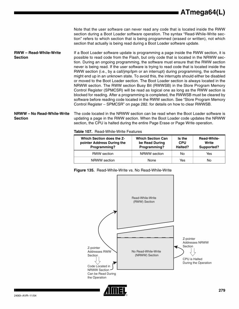
ATmega64(L)
Note that the user software can never read any code that is located inside the RWWsection during a Boot Loader software operation. The syntax “Read-While-Write sec-tion” refers to which section that is being programmed (erased or written), not whichsection that actually is being read during a Boot Loader software update.
RWW – Read-While-Write Section
If a Boot Loader software update is programming a page inside the RWW section, it ispossible to read code from the Flash, but only code that is located in the NRWW sec-tion. During an ongoing programming, the software must ensure that the RWW sectionnever is being read. If the user software is trying to read code that is located inside theRWW section (i.e., by a call/jmp/lpm or an interrupt) during programming, the softwaremight end up in an unknown state. To avoid this, the interrupts should either be disabledor moved to the Boot Loader section. The Boot Loader section is always located in theNRWW section. The RWW section Busy Bit (RWWSB) in the Store Program MemoryControl Register (SPMCSR) will be read as logical one as long as the RWW section isblocked for reading. After a programming is completed, the RWWSB must be cleared bysoftware before reading code located in the RWW section. See “Store Program MemoryControl Register – SPMCSR” on page 282. for details on how to clear RWWSB.
NRWW – No Read-While-Write Section
The code located in the NRWW section can be read when the Boot Loader software isupdating a page in the RWW section. When the Boot Loader code updates the NRWWsection, the CPU is halted during the entire Page Erase or Page Write operation.
Figure 135. Read-While-Write vs. No Read-While-Write
Table 107. Read-While-Write Features
Which Section does the Z-pointer Address During the
Programming?
Which Section Can be Read During Programming?
Is the CPU
Halted?
Read-While-Write
Supported?
RWW section NRWW section No Yes
NRWW section None Yes No
Read-While-Write(RWW) Section
No Read-While-Write (NRWW) Section
Z-pointerAddresses RWWSection
Z-pointerAddresses NRWWSection
CPU is HaltedDuring the Operation
Code Located in NRWW SectionCan be Read Duringthe Operation
2792490I–AVR–11/04
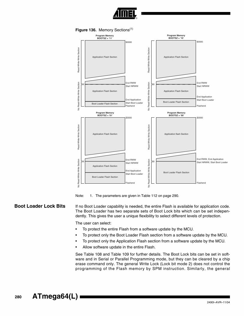
Figure 136. Memory Sections(1)
Note: 1. The parameters are given in Table 112 on page 290.
Boot Loader Lock Bits If no Boot Loader capability is needed, the entire Flash is available for application code.The Boot Loader has two separate sets of Boot Lock bits which can be set indepen-dently. This gives the user a unique flexibility to select different levels of protection.
The user can select:
• To protect the entire Flash from a software update by the MCU.
• To protect only the Boot Loader Flash section from a software update by the MCU.
• To protect only the Application Flash section from a software update by the MCU.
• Allow software update in the entire Flash.
See Table 108 and Table 109 for further details. The Boot Lock bits can be set in soft-ware and in Serial or Parallel Programming mode, but they can be cleared by a chiperase command only. The general Write Lock (Lock bit mode 2) does not control theprogramming of the Flash memory by SPM instruction. Similarly, the general
$0000
Flashend
Program MemoryBOOTSZ = '11'
Application Flash Section
Boot Loader Flash SectionFlashend
Program MemoryBOOTSZ = '10'
$0000
Program MemoryBOOTSZ = '01'
Program MemoryBOOTSZ = '00'
Application Flash Section
Boot Loader Flash Section
$0000
Flashend
Application Flash Section
Flashend
End RWW
Start NRWW
Application flash Section
Boot Loader Flash Section
Boot Loader Flash Section
End RWW
Start NRWW
End RWW
Start NRWW
$0000
End RWW, End Application
Start NRWW, Start Boot Loader
Application Flash SectionApplication Flash Section
Application Flash Section
Rea
d-W
hile
-Writ
e S
ectio
nN
o R
ead-
Whi
le-W
rite
Sec
tion
Rea
d-W
hile
-Writ
e S
ectio
nN
o R
ead-
Whi
le-W
rite
Sec
tion
Rea
d-W
hile
-Writ
e S
ectio
nN
o R
ead-
Whi
le-W
rite
Sec
tion
Rea
d-W
hile
-Writ
e S
ectio
nN
o R
ead-
Whi
le-W
rite
Sec
tion
End Application
Start Boot Loader
End Application
Start Boot Loader
End Application
Start Boot Loader
280 ATmega64(L)2490I–AVR–11/04
ATmega64(L)
Read/Write Lock (Lock bit mode 3) does not control reading nor writing by LPM/SPM, ifit is attempted.
Note: 1. “1” means unprogrammed, “0” means programmed
Note: 1. “1” means unprogrammed, “0” means programmed
Table 108. Boot Lock Bit0 Protection Modes (Application Section)(1)
BLB0 Mode BLB02 BLB01 Protection
1 1 1 No restrictions for SPM or LPM accessing the Application section.
2 1 0 SPM is not allowed to write to the Application section.
3 0 0 SPM is not allowed to write to the Application section, and LPM executing from the Boot Loader section is not allowed to read from the Application section. If Interrupt Vectors are placed in the Boot Loader section, interrupts are disabled while executing from the Application section.
4 0 1 LPM executing from the Boot Loader section is not allowed to read from the Application section. If Interrupt Vectors are placed in the Boot Loader section, interrupts are disabled while executing from the Application section.
Table 109. Boot Lock Bit1 Protection Modes (Boot Loader Section)(1)
BLB1 Mode BLB12 BLB11 Protection
1 1 1 No restrictions for SPM or LPM accessing the Boot Loader section.
2 1 0 SPM is not allowed to write to the Boot Loader section.
3 0 0 SPM is not allowed to write to the Boot Loader section, and LPM executing from the Application section is not allowed to read from the Boot Loader section. If Interrupt Vectors are placed in the Application section, interrupts are disabled while executing from the Boot Loader section.
4 0 1 LPM executing from the Application section is not allowed to read from the Boot Loader section. If Interrupt Vectors are placed in the Application section, interrupts are disabled while executing from the Boot Loader section.
2812490I–AVR–11/04
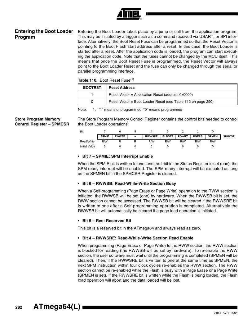
Entering the Boot Loader Program
Entering the Boot Loader takes place by a jump or call from the application program.This may be initiated by a trigger such as a command received via USART, or SPI inter-face. Alternatively, the Boot Reset Fuse can be programmed so that the Reset Vector ispointing to the Boot Flash start address after a reset. In this case, the Boot Loader isstarted after a reset. After the application code is loaded, the program can start execut-ing the application code. Note that the fuses cannot be changed by the MCU itself. Thismeans that once the Boot Reset Fuse is programmed, the Reset Vector will alwayspoint to the Boot Loader Reset and the fuse can only be changed through the serial orparallel programming interface.
Note: 1. “1” means unprogrammed, “0” means programmed
Store Program Memory Control Register – SPMCSR
The Store Program Memory Control Register contains the control bits needed to controlthe Boot Loader operations.
• Bit 7 – SPMIE: SPM Interrupt Enable
When the SPMIE bit is written to one, and the I-bit in the Status Register is set (one), theSPM ready interrupt will be enabled. The SPM ready interrupt will be executed as longas the SPMEN bit in the SPMCSR Register is cleared.
• Bit 6 – RWWSB: Read-While-Write Section Busy
When a Self-programming (Page Erase or Page Write) operation to the RWW section isinitiated, the RWWSB will be set (one) by hardware. When the RWWSB bit is set, theRWW section cannot be accessed. The RWWSB bit will be cleared if the RWWSRE bitis written to one after a Self-programming operation is completed. Alternatively theRWWSB bit will automatically be cleared if a page load operation is initiated.
• Bit 5 – Res: Reserved Bit
This bit is a reserved bit in the ATmega64 and always read as zero.
• Bit 4 – RWWSRE: Read-While-Write Section Read Enable
When programming (Page Erase or Page Write) to the RWW section, the RWW sectionis blocked for reading (the RWWSB will be set by hardware). To re-enable the RWWsection, the user software must wait until the programming is completed (SPMEN will becleared). Then, if the RWWSRE bit is written to one at the same time as SPMEN, thenext SPM instruction within four clock cycles re-enables the RWW section. The RWWsection cannot be re-enabled while the Flash is busy with a Page Erase or a Page Write(SPMEN is set). If the RWWSRE bit is written while the Flash is being loaded, the Flashload operation will abort and the data loaded will be lost.
Table 110. Boot Reset Fuse(1)
BOOTRST Reset Address
1 Reset Vector = Application Reset (address 0x0000)
0 Reset Vector = Boot Loader Reset (see Table 112 on page 290)
Bit 7 6 5 4 3 2 1 0
SPMIE RWWSB – RWWSRE BLBSET PGWRT PGERS SPMEN SPMCSR
Read/Write R/W R R R/W R/W R/W R/W R/W
Initial Value 0 0 0 0 0 0 0 0
282 ATmega64(L)2490I–AVR–11/04
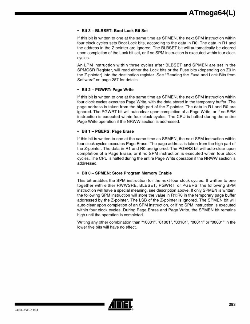
ATmega64(L)
• Bit 3 – BLBSET: Boot Lock Bit Set
If this bit is written to one at the same time as SPMEN, the next SPM instruction withinfour clock cycles sets Boot Lock bits, according to the data in R0. The data in R1 andthe address in the Z-pointer are ignored. The BLBSET bit will automatically be clearedupon completion of the Lock bit set, or if no SPM instruction is executed within four clockcycles.
An LPM instruction within three cycles after BLBSET and SPMEN are set in theSPMCSR Register, will read either the Lock bits or the Fuse bits (depending on Z0 inthe Z-pointer) into the destination register. See “Reading the Fuse and Lock Bits fromSoftware” on page 287 for details.
• Bit 2 – PGWRT: Page Write
If this bit is written to one at the same time as SPMEN, the next SPM instruction withinfour clock cycles executes Page Write, with the data stored in the temporary buffer. Thepage address is taken from the high part of the Z-pointer. The data in R1 and R0 areignored. The PGWRT bit will auto-clear upon completion of a Page Write, or if no SPMinstruction is executed within four clock cycles. The CPU is halted during the entirePage Write operation if the NRWW section is addressed.
• Bit 1 – PGERS: Page Erase
If this bit is written to one at the same time as SPMEN, the next SPM instruction withinfour clock cycles executes Page Erase. The page address is taken from the high part ofthe Z-pointer. The data in R1 and R0 are ignored. The PGERS bit will auto-clear uponcompletion of a Page Erase, or if no SPM instruction is executed within four clockcycles. The CPU is halted during the entire Page Write operation if the NRWW section isaddressed.
• Bit 0 – SPMEN: Store Program Memory Enable
This bit enables the SPM instruction for the next four clock cycles. If written to onetogether with either RWWSRE, BLBSET, PGWRT’ or PGERS, the following SPMinstruction will have a special meaning, see description above. If only SPMEN is written,the following SPM instruction will store the value in R1:R0 in the temporary page bufferaddressed by the Z-pointer. The LSB of the Z-pointer is ignored. The SPMEN bit willauto-clear upon completion of an SPM instruction, or if no SPM instruction is executedwithin four clock cycles. During Page Erase and Page Write, the SPMEN bit remainshigh until the operation is completed.
Writing any other combination than “10001”, “01001”, “00101”, “00011” or “00001” in thelower five bits will have no effect.
2832490I–AVR–11/04
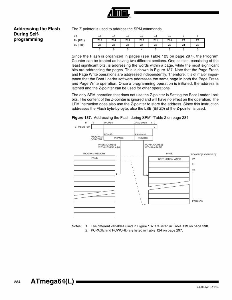
Addressing the Flash During Self-programming
The Z-pointer is used to address the SPM commands.
Since the Flash is organized in pages (see Table 123 on page 297), the ProgramCounter can be treated as having two different sections. One section, consisting of theleast significant bits, is addressing the words within a page, while the most significantbits are addressing the pages. This is shown in Figure 137. Note that the Page Eraseand Page Write operations are addressed independently. Therefore, it is of major impor-tance that the Boot Loader software addresses the same page in both the Page Eraseand Page Write operation. Once a programming operation is initiated, the address islatched and the Z-pointer can be used for other operations.
The only SPM operation that does not use the Z-pointer is Setting the Boot Loader Lockbits. The content of the Z-pointer is ignored and will have no effect on the operation. TheLPM instruction does also use the Z-pointer to store the address. Since this instructionaddresses the Flash byte-by-byte, also the LSB (Bit Z0) of the Z-pointer is used.
Figure 137. Addressing the Flash during SPM(1)Table 2 on page 284
Notes: 1. The different variables used in Figure 137 are listed in Table 113 on page 290. 2. PCPAGE and PCWORD are listed in Table 124 on page 297.
Bit 15 14 13 12 11 10 9 8
ZH (R31) Z15 Z14 Z13 Z12 Z11 Z10 Z9 Z8ZL (R30) Z7 Z6 Z5 Z4 Z3 Z2 Z1 Z0
7 6 5 4 3 2 1 0
PROGRAM MEMORY
0115
Z - REGISTER
BIT
0
ZPAGEMSB
WORD ADDRESSWITHIN A PAGE
PAGE ADDRESSWITHIN THE FLASH
ZPCMSB
INSTRUCTION WORD
PAGE PCWORD[PAGEMSB:0]:
00
01
02
PAGEEND
PAGE
PCWORDPCPAGE
PCMSB PAGEMSBPROGRAMCOUNTER
284 ATmega64(L)2490I–AVR–11/04
ATmega64(L)
Self-programming the Flash
The program memory is updated in a page-by-page fashion. Before programming apage with the data stored in the temporary page buffer, the page must be erased. Thetemporary page buffer is filled one word at a time using SPM and the buffer can be filledeither before the Page Erase command or between a Page Erase and a Page Writeoperation:
Alternative 1, fill the buffer before a Page Erase:
• Fill temporary page buffer
• Perform a Page Erase
• Perform a Page Write
Alternative 2, fill the buffer after Page Erase:
• Perform a Page Erase
• Fill temporary page buffer
• Perform a Page Write
If only a part of the page needs to be changed, the rest of the page must be stored (forexample in the temporary page buffer) before the erase, and then be rewritten. Whenusing Alternative 1, the boot loader provides an effective Read-Modify-Write featurewhich allows the user software to first read the page, do the necessary changes, andthen write back the modified data. If Alternative 2 is used, it is not possible to read theold data while loading since the page is already erased. The temporary page buffer canbe accessed in a random sequence. It is essential that the page address used in boththe Page Erase and Page Write operation is addressing the same page. See “SimpleAssembly Code Example for a Boot Loader” on page 288 for an assembly codeexample.
Performing Page Erase by SPM
To execute Page Erase, set up the address in the Z-pointer, write “X0000011” toSPMCSR and execute SPM within four clock cycles after writing SPMCSR. The data inR1 and R0 is ignored. The page address must be written to PCPAGE in the Z-register.Other bits in the Z-pointer must be written zero during this operation.
• Page Erase to the RWW section: The NRWW section can be read during the Page Erase.
• Page Erase to the NRWW section: The CPU is halted during the operation.
Filling the Temporary Buffer (Page Loading)
To write an instruction word, set up the address in the Z-pointer and data in R1:R0, write“00000001” to SPMCSR and execute SPM within four clock cycles after writingSPMCSR. The content of PCWORD in the Z-register is used to address the data in thetemporary buffer. The temporary buffer will auto-erase after a Page Write operation orby writing the RWWSRE bit in SPMCSR. It is also erased after a System Reset. Notethat it is not possible to write more than one time to each address without erasing thetemporary buffer.Note: If the EEPROM is written in the middle of an SPM Page Load operation, all data loaded
will be lost.
Performing a Page Write To execute Page Write, set up the address in the Z-pointer, write “X0000101” toSPMCSR and execute SPM within four clock cycles after writing SPMCSR. The data inR1 and R0 is ignored. The page address must be written to PCPAGE. Other bits in theZ-pointer must be written zero during this operation.
• Page Write to the RWW section: The NRWW section can be read during the Page Write.
• Page Write to the NRWW section: The CPU is halted during the operation.
2852490I–AVR–11/04
Using the SPM Interrupt If the SPM interrupt is enabled, the SPM interrupt will generate a constant interruptwhen the SPMEN bit in SPMCSR is cleared. This means that the interrupt can be usedinstead of polling the SPMCSR Register in software. When using the SPM interrupt, theInterrupt Vectors should be moved to the BLS section to avoid that an interrupt isaccessing the RWW section when it is blocked for reading. How to move the interruptsis described in “Interrupts” on page 60.
Consideration While Updating BLS
Special care must be taken if the user allows the Boot Loader section to be updated byleaving Boot Lock bit11 unprogrammed. An accidental write to the Boot Loader itself cancorrupt the entire Boot Loader, and further software updates might be impossible. If it isnot necessary to change the Boot Loader software itself, it is recommended to programthe Boot Lock bit11 to protect the Boot Loader software from any internal softwarechanges.
Prevent Reading the RWW Section During Self-programming
During Self-programming (either Page Erase or Page Write), the RWW section isalways blocked for reading. The user software itself must prevent that this section isaddressed during the Self-programming operation. The RWWSB in the SPMCSR will beset as long as the RWW section is busy. During Self-programming the Interrupt Vectortable should be moved to the BLS as described in “Interrupts” on page 60, or the inter-rupts must be disabled. Before addressing the RWW section after the programming iscompleted, the user software must clear the RWWSB by writing the RWWSRE. See“Simple Assembly Code Example for a Boot Loader” on page 288 for an example.
Setting the Boot Loader Lock Bits by SPM
To set the Boot Loader Lock bits, write the desired data to R0, write “X0001001” toSPMCSR and execute SPM within four clock cycles after writing SPMCSR. The onlyaccessible Lock bits are the Boot Lock bits that may prevent the Application and BootLoader section from any software update by the MCU.
See Table 108 and Table 109 for how the different settings of the Boot Loader Bitsaffect the Flash access.
If bits 5..2 in R0 are cleared (zero), the corresponding Boot Lock bit will be programmedif an SPM instruction is executed within four cycles after BLBSET and SPMEN are set inSPMCSR. The Z-pointer is don’t care during this operation, but for future compatibility itis recommended to load the Z-pointer with 0x0001 (same as used for reading the Lockbits). For future compatibility It is also recommended to set bits 7, 6, 1, and 0 in R0 to “1”when writing the Lock bits. When programming the Lock bits the entire Flash can beread during the operation.
EEPROM Write Prevents Writing to SPMCSR
Note that an EEPROM write operation will block all software programming to Flash.Reading the Fuses and Lock bits from software will also be prevented during theEEPROM write operation. It is recommended that the user checks the status bit (EEWE)in the EECR Register and verifies that the bit is cleared before writing to the SPMCSRRegister.
Bit 7 6 5 4 3 2 1 0
R0 1 1 BLB12 BLB11 BLB02 BLB01 1 1
286 ATmega64(L)2490I–AVR–11/04
ATmega64(L)
Reading the Fuse and Lock Bits from Software
It is possible to read both the Fuse and Lock bits from software. To read the Lock bits,load the Z-pointer with 0x0001 and set the BLBSET and SPMEN bits in SPMCSR.When an LPM instruction is executed within three CPU cycles after the BLBSET andSPMEN bits are set in SPMCSR, the value of the Lock bits will be loaded in the destina-tion register. The BLBSET and SPMEN bits will auto-clear upon completion of readingthe Lock bits or if no LPM instruction is executed within three CPU cycles or no SPMinstruction is executed within four CPU cycles. When BLBSET and SPMEN are cleared,LPM will work as described in the AVR Instruction Set Reference Manual.
The algorithm for reading the Fuse Low bits is similar to the one described above forreading the Lock bits. To read the Fuse Low bits, load the Z-pointer with 0x0000 and setthe BLBSET and SPMEN bits in SPMCSR. When an LPM instruction is executed withinthree cycles after the BLBSET and SPMEN bits are set in the SPMCSR, the value of theFuse Low bits (FLB) will be loaded in the destination register as shown below. Refer toTable 119 on page 293 for a detailed description and mapping of the Fuse Low bits.
Similarly, when reading the Fuse High bits, load 0x0003 in the Z-pointer. When an LPMinstruction is executed within three cycles after the BLBSET and SPMEN bits are set inthe SPMCSR, the value of the Fuse High bits (FHB) will be loaded in the destinationregister as shown below. Refer to Table 118 on page 293 for detailed description andmapping of the Fuse High bits.
When reading the Extended Fuse bits, load 0x0002 in the Z-pointer. When an LPMinstruction is executed within three cycles after the BLBSET and SPMEN bits are set inthe SPMCSR, the value of the Extended Fuse bits (EFB) will be loaded in the destina-tion register as shown below. Refer to Table 117 on page 292 for detailed descriptionand mapping of the Fuse High bits.
Fuse and Lock bits that are programmed will be read as zero. Fuse and Lock bits thatare unprogrammed will be read as one.
Preventing Flash Corruption During periods of low VCC, the Flash program can be corrupted because the supply volt-age is too low for the CPU and the Flash to operate properly. These issues are the sameas for board level systems using the Flash, and the same design solutions should beapplied.
A Flash program corruption can be caused by two situations when the voltage is too low.First, a regular write sequence to the Flash requires a minimum voltage to operate cor-rectly. Second, the CPU itself can execute instructions incorrectly, if the supply voltagefor executing instructions is too low.
Flash corruption can easily be avoided by following these design recommendations (oneis sufficient):
Bit 7 6 5 4 3 2 1 0
Rd – – BLB12 BLB11 BLB02 BLB01 LB2 LB1
Bit 7 6 5 4 3 2 1 0
Rd FLB7 FLB6 FLB5 FLB4 FLB3 FLB2 FLB1 FLB0
Bit 7 6 5 4 3 2 1 0
Rd FHB7 FHB6 FHB5 FHB4 FHB3 FHB2 FHB1 FHB0
Bit 7 6 5 4 3 2 1 0
Rd – – – – – – EFB1 EFB0
2872490I–AVR–11/04
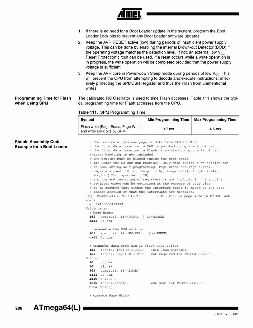
1. If there is no need for a Boot Loader update in the system, program the Boot Loader Lock bits to prevent any Boot Loader software updates.
2. Keep the AVR RESET active (low) during periods of insufficient power supply voltage. This can be done by enabling the internal Brown-out Detector (BOD) if the operating voltage matches the detection level. If not, an external low VCC Reset Protection circuit can be used. If a reset occurs while a write operation is in progress, the write operation will be completed provided that the power supply voltage is sufficient.
3. Keep the AVR core in Power-down Sleep mode during periods of low VCC. This will prevent the CPU from attempting to decode and execute instructions, effec-tively protecting the SPMCSR Register and thus the Flash from unintentional writes.
Programming Time for Flash when Using SPM
The calibrated RC Oscillator is used to time Flash accesses. Table 111 shows the typi-cal programming time for Flash accesses from the CPU.
Simple Assembly Code Example for a Boot Loader
;-the routine writes one page of data from RAM to Flash; the first data location in RAM is pointed to by the Y pointer; the first data location in Flash is pointed to by the Z-pointer;-error handling is not included;-the routine must be placed inside the boot space; (at least the Do_spm sub routine). Only code inside NRWW section can; be read during self-programming (Page Erase and Page Write).;-registers used: r0, r1, temp1 (r16), temp2 (r17), looplo (r24), ; loophi (r25), spmcrval (r20); storing and restoring of registers is not included in the routine; register usage can be optimized at the expense of code size;-It is assumed that either the interrupt table is moved to the Boot; loader section or that the interrupts are disabled.
.equ PAGESIZEB = PAGESIZE*2 ;PAGESIZEB is page size in BYTES, not words.org SMALLBOOTSTARTWrite_page:; Page Eraseldi spmcrval, (1<<PGERS) | (1<<SPMEN)call Do_spm
; re-enable the RWW sectionldi spmcrval, (1<<RWWSRE) | (1<<SPMEN)call Do_spm
; transfer data from RAM to Flash page bufferldi looplo, low(PAGESIZEB) ;init loop variableldi loophi, high(PAGESIZEB) ;not required for PAGESIZEB<=256
Wrloop:ld r0, Y+ld r1, Y+ldi spmcrval, (1<<SPMEN)call Do_spmadiw ZH:ZL, 2sbiw loophi:looplo, 2 ;use subi for PAGESIZEB<=256brne Wrloop
; execute Page Write
Table 111. SPM Programming Time
Symbol Min Programming Time Max Programming Time
Flash write (Page Erase, Page Write, and write Lock bits by SPM)
3.7 ms 4.5 ms
288 ATmega64(L)2490I–AVR–11/04
ATmega64(L)
subi ZL, low(PAGESIZEB) ;restore pointersbci ZH, high(PAGESIZEB) ;not required for PAGESIZEB<=256ldi spmcrval, (1<<PGWRT) | (1<<SPMEN)call Do_spm
; re-enable the RWW sectionldi spmcrval, (1<<RWWSRE) | (1<<SPMEN)call Do_spm
; read back and check, optionalldi looplo, low(PAGESIZEB) ;init loop variableldi loophi, high(PAGESIZEB) ;not required for PAGESIZEB<=256subi YL, low(PAGESIZEB) ;restore pointersbci YH, high(PAGESIZEB)
Rdloop:lpm r0, Z+ld r1, Y+cpse r0, r1jmp Errorsbiw loophi:looplo, 1 ;use subi for PAGESIZEB<=256brne Rdloop
; return to RWW section; verify that RWW section is safe to read
Return:lds temp1, SPMCSRsbrs temp1, RWWSB ; If RWWSB is set, the RWW section is not ready
yetret; re-enable the RWW sectionldi spmcrval, (1<<RWWSRE) | (1<<SPMEN)call Do_spmrjmp Return
Do_spm:; check for previous SPM complete
Wait_spm:lds temp1, SPMCSRsbrc temp1, SPMENrjmp Wait_spm; input: spmcrval determines SPM action; disable interrupts if enabled, store statusin temp2, SREGcli; check that no EEPROM write access is present
Wait_ee:sbic EECR, EEWErjmp Wait_ee; SPM timed sequencests SPMCSR, spmcrvalspm; restore SREG (to enable interrupts if originally enabled)out SREG, temp2ret
2892490I–AVR–11/04
ATmega64 Boot Loader Parameters
In Table 112 through Table 114, the parameters used in the description of the Self-pro-gramming are given.
Note: 1. The different BOOTSZ Fuse configurations are shown in Figure 136
Note: 1. For details about these two section, see “NRWW – No Read-While-Write Section” onpage 279 and “RWW – Read-While-Write Section” on page 279
Notes: 1. Z0: should be zero for all SPM commands, byte select for the LPM instruction.2. See “Addressing the Flash During Self-programming” on page 284 for details about
the use of Z-pointer during Self-programming.
Table 112. Boot Size Configuration(1)
BOOTSZ1
BOOTSZ0
Boot Size Pages
Appli-cation Flash Section
Boot Loader Flash Section
End Applic-ation Section
Boot Reset Address (Start Boot Loader Section)
1 1512 words
40x0000 - 0x7DFF
0x7E00 - 0x7FFF
0x7DFF 0x7E00
1 01024 words
80x0000 - 0x7BFF
0x7C00 - 0x7FFF
0x7BFF 0x7C00
0 12048 words
160x0000 - 0x77FF
0x7800 - 0x7FFF
0x77FF 0x7800
0 04096 words
320x0000 - 0x6FFF
0x7000 - 0x7FFF
0x6FFF 0x7000
Table 113. Read-While-Write Limit(1)
Section Pages Address
Read-While-Write (RWW) 224 0x0000 - 0x6FFF
No Read-While-Write (NRWW) 32 0x7000 - 0x7FFF
Table 114. Explanation of Different Variables Used in Figure 137 and the Mapping tothe Z-pointer(1)(2)
VariableCorresponding
Z-value Description
PCMSB14 Most significant bit in the Program Counter.
(The Program Counter is 15 bits PC[14:0]).
PAGEMSB6 Most significant bit which is used to address the
words within one page (128 words in a page requires seven bits PC [6:0]).
ZPCMSBZ15 Bit in Z-register that is mapped to PCMSB.
Because Z0 is not used, the ZPCMSB equals PCMSB + 1.
ZPAGEMSBZ7 Bit in Z-register that is mapped to PAGEMSB.
Because Z0 is not used, the ZPAGEMSB equals PAGEMSB + 1.
PCPAGEPC[14:7] Z15:Z8 Program Counter page address: Page select,
for Page Erase and Page Write
PCWORDPC[6:0] Z7:Z1 Program Counter word address: Word select,
for filling temporary buffer (must be zero during Page Write operation)
290 ATmega64(L)2490I–AVR–11/04
ATmega64(L)
Memory Programming
Program and Data Memory Lock Bits
The ATmega64 provides six Lock bits which can be left unprogrammed (“1”) or can beprogrammed (“0”) to obtain the additional features listed in Table 116. The Lock bits canonly be erased to “1” with the Chip Erase command.
Note: 1. “1” means unprogrammed, “0” means programmed
Table 115. Lock Bit Byte(1)
Lock Bit Byte Bit no Description Default Value
7 – 1 (unprogrammed)
6 – 1 (unprogrammed)
BLB12 5 Boot Lock bit 1 (unprogrammed)
BLB11 4 Boot Lock bit 1 (unprogrammed)
BLB02 3 Boot Lock bit 1 (unprogrammed)
BLB01 2 Boot Lock bit 1 (unprogrammed)
LB2 1 Lock bit 1 (unprogrammed)
LB1 0 Lock bit 1 (unprogrammed)
Table 116. Lock Bit Protection Modes(2)
Memory Lock Bits Protection Type
LB Mode LB2 LB1
1 1 1 No memory lock features enabled.
2 1 0 Further programming of the Flash and EEPROM is disabled in Parallel and SPI/JTAG Serial Programming mode. The Fuse bits are locked in both Serial and Parallel Programming mode.(1)
3 0 0 Further programming and verification of the Flash and EEPROM is disabled in Parallel and SPI/JTAG Serial Programming mode. The Fuse bits are locked in both Serial and Parallel Programming mode.(1)
BLB0 Mode BLB02 BLB01
1 1 1 No restrictions for SPM or LPM accessing the Application section.
2 1 0 SPM is not allowed to write to the Application section.
3 0 0 SPM is not allowed to write to the Application section, and LPM executing from the Boot Loader section is not allowed to read from the Application section. If Interrupt Vectors are placed in the Boot Loader section, interrupts are disabled while executing from the Application section.
4 0 1 LPM executing from the Boot Loader section is not allowed to read from the Application section. If Interrupt Vectors are placed in the Boot Loader section, interrupts are disabled while executing from the Application section.
BLB1 Mode BLB12 BLB11
2912490I–AVR–11/04
Notes: 1. Program the Fuse bits before programming the Lock bits.2. “1” means unprogrammed, “0” means programmed
Fuse Bits The ATmega64 has three fuse bytes. Table 117 - Table 119 describe briefly the func-tionality of all the fuses and how they are mapped into the fuse bytes. Note that thefuses are read as logical zero, “0”, if they are programmed.
Notes: 1. See “ATmega103 and ATmega64 Compatibility” on page 4 for details.2. See “Watchdog Timer Control Register – WDTCR” on page 56 for details.
1 1 1 No restrictions for SPM or LPM accessing the Boot Loader section.
2 1 0 SPM is not allowed to write to the Boot Loader section.
3 0 0 SPM is not allowed to write to the Boot Loader section, and LPM executing from the Application section is not allowed to read from the Boot Loader section. If Interrupt Vectors are placed in the Application section, interrupts are disabled while executing from the Boot Loader section.
4 0 1 LPM executing from the Application section is not allowed to read from the Boot Loader section. If Interrupt Vectors are placed in the Application section, interrupts are disabled while executing from the Boot Loader section.
Table 116. Lock Bit Protection Modes(2) (Continued)
Memory Lock Bits Protection Type
Table 117. Extended Fuse Byte
Fuse Low Byte Bit no Description Default Value
– 7 – 1
– 6 – 1
– 5 – 1
– 4 – 1
– 3 – 1
– 2 – 1
M103C(1) 1 ATmega103 compatibility mode 0 (programmed)
WDTON(2) 0 Watchdog Timer always on 1 (unprogrammed)
292 ATmega64(L)2490I–AVR–11/04
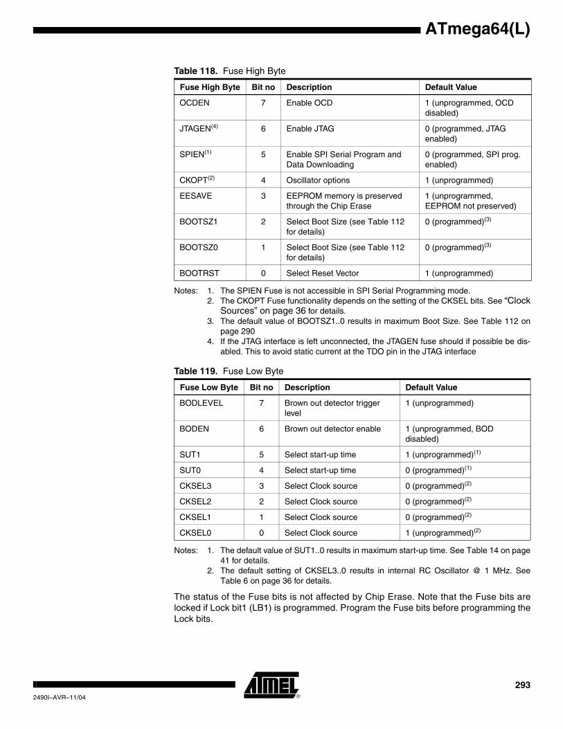
ATmega64(L)
Notes: 1. The SPIEN Fuse is not accessible in SPI Serial Programming mode.2. The CKOPT Fuse functionality depends on the setting of the CKSEL bits. See “Clock
Sources” on page 36 for details.3. The default value of BOOTSZ1..0 results in maximum Boot Size. See Table 112 on
page 2904. If the JTAG interface is left unconnected, the JTAGEN fuse should if possible be dis-
abled. This to avoid static current at the TDO pin in the JTAG interface
Notes: 1. The default value of SUT1..0 results in maximum start-up time. See Table 14 on page41 for details.
2. The default setting of CKSEL3..0 results in internal RC Oscillator @ 1 MHz. SeeTable 6 on page 36 for details.
The status of the Fuse bits is not affected by Chip Erase. Note that the Fuse bits arelocked if Lock bit1 (LB1) is programmed. Program the Fuse bits before programming theLock bits.
Table 118. Fuse High Byte
Fuse High Byte Bit no Description Default Value
OCDEN 7 Enable OCD 1 (unprogrammed, OCD disabled)
JTAGEN(4) 6 Enable JTAG 0 (programmed, JTAG enabled)
SPIEN(1) 5 Enable SPI Serial Program and Data Downloading
0 (programmed, SPI prog. enabled)
CKOPT(2) 4 Oscillator options 1 (unprogrammed)
EESAVE 3 EEPROM memory is preserved through the Chip Erase
1 (unprogrammed, EEPROM not preserved)
BOOTSZ1 2 Select Boot Size (see Table 112 for details)
0 (programmed)(3)
BOOTSZ0 1 Select Boot Size (see Table 112 for details)
0 (programmed)(3)
BOOTRST 0 Select Reset Vector 1 (unprogrammed)
Table 119. Fuse Low Byte
Fuse Low Byte Bit no Description Default Value
BODLEVEL 7 Brown out detector trigger level
1 (unprogrammed)
BODEN 6 Brown out detector enable 1 (unprogrammed, BOD disabled)
SUT1 5 Select start-up time 1 (unprogrammed)(1)
SUT0 4 Select start-up time 0 (programmed)(1)
CKSEL3 3 Select Clock source 0 (programmed)(2)
CKSEL2 2 Select Clock source 0 (programmed)(2)
CKSEL1 1 Select Clock source 0 (programmed)(2)
CKSEL0 0 Select Clock source 1 (unprogrammed)(2)
2932490I–AVR–11/04
Latching of Fuses The fuse values are latched when the device enters Programming mode and changes ofthe fuse values will have no effect until the part leaves Programming mode. This doesnot apply to the EESAVE Fuse which will take effect once it is programmed. The fusesare also latched on Power-up in Normal mode.
Signature Bytes All Atmel microcontrollers have a 3-byte signature code which identifies the device. Thiscode can be read in both Serial and Parallel mode, also when the device is locked. Thethree bytes reside in a separate address space.
For the ATmega64 the signature bytes are:
1. 0x000: 0x1E (indicates manufactured by Atmel)
2. 0x001: 0x96 (indicates 64KB Flash memory)
3. 0x002: 0x02 (indicates ATmega64 device when 0x001 is 0x96)
Calibration Byte The ATmega64 stores four different calibration values for the internal RC Oscillator.These bytes resides in the signature row high byte of the addresses 0x000, 0x0001,0x0002, and 0x0003 for 1, 2, 4, and 8 MHz respectively. During Reset, the 1 MHz valueis automatically loaded into the OSCCAL Register. If other frequencies are used, thecalibration value has to be loaded manually, see “Oscillator Calibration Register – OSC-CAL(1)” on page 41 for details.
Parallel Programming Parameters, Pin Mapping, and Commands
This section describes how to parallel program and verify Flash Program memory,EEPROM Data memory, Memory Lock bits, and Fuse bits in the ATmega64. Pulses areassumed to be at least 250 ns unless otherwise noted.
Signal Names In this section, some pins of the ATmega64 are referenced by signal names describingtheir functionality during parallel programming, see Figure 138 and Table 120. Pins notdescribed in the following table are referenced by pin names.
The XA1/XA0 pins determine the action executed when the XTAL1 pin is given a posi-tive pulse. The bit coding is shown in Table 122.
When pulsing WR or OE, the command loaded determines the action executed. The dif-ferent Commands are shown in Table 123.
294 ATmega64(L)2490I–AVR–11/04
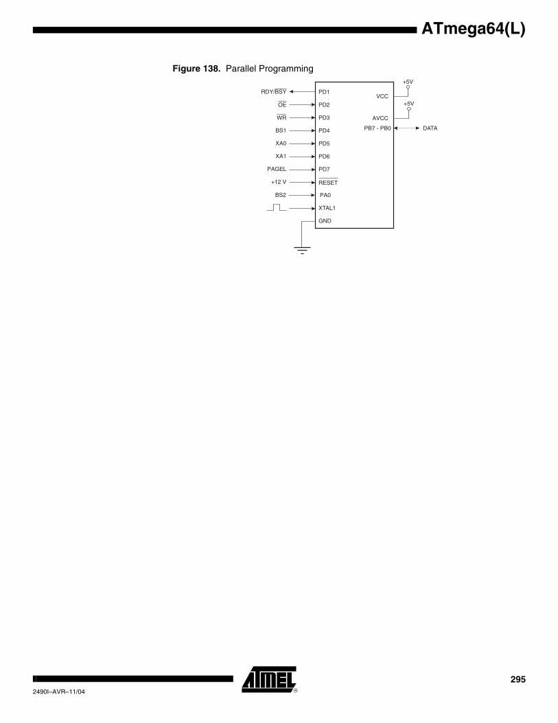
ATmega64(L)
Figure 138. Parallel Programming
VCC
+5V
GND
XTAL1
PD1
PD2
PD3
PD4
PD5
PD6
PB7 - PB0 DATA
RESET
PD7
+12 V
BS1
XA0
XA1
OE
RDY/BSY
PAGEL
PA0
WR
BS2
AVCC
+5V
2952490I–AVR–11/04
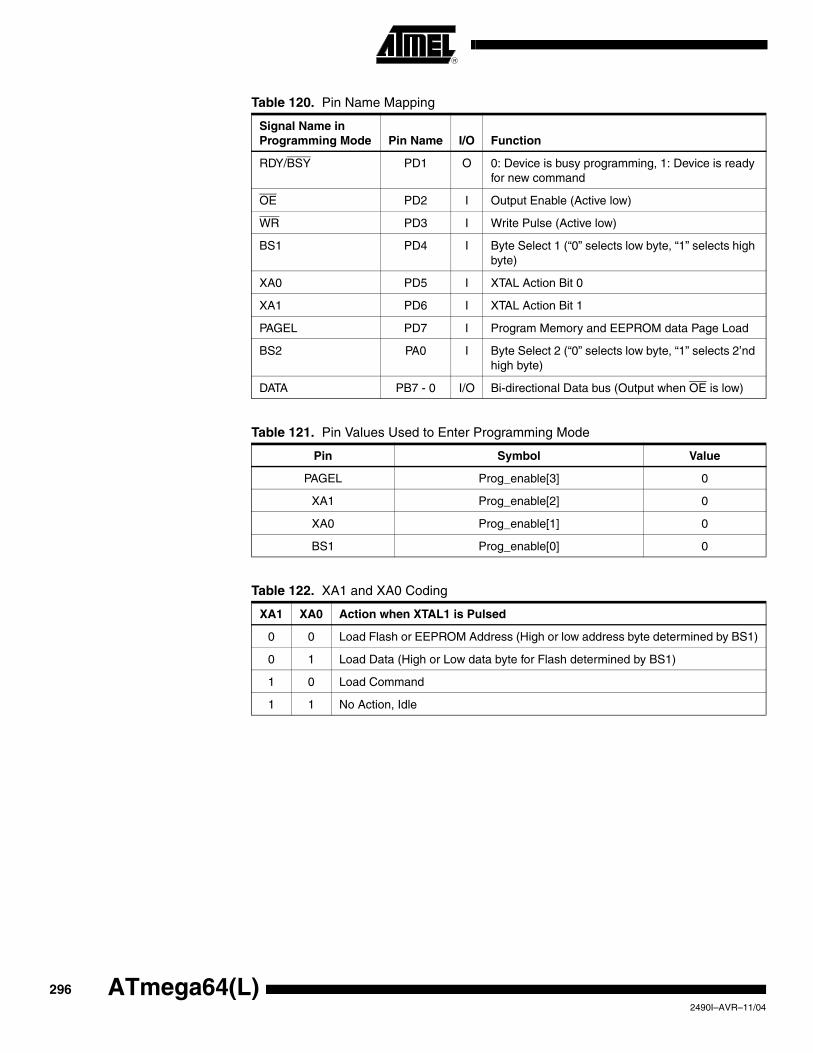
Table 120. Pin Name Mapping
Signal Name in Programming Mode Pin Name I/O Function
RDY/BSY PD1 O 0: Device is busy programming, 1: Device is ready for new command
OE PD2 I Output Enable (Active low)
WR PD3 I Write Pulse (Active low)
BS1 PD4 I Byte Select 1 (“0” selects low byte, “1” selects high byte)
XA0 PD5 I XTAL Action Bit 0
XA1 PD6 I XTAL Action Bit 1
PAGEL PD7 I Program Memory and EEPROM data Page Load
BS2 PA0 I Byte Select 2 (“0” selects low byte, “1” selects 2’nd high byte)
DATA PB7 - 0 I/O Bi-directional Data bus (Output when OE is low)
Table 121. Pin Values Used to Enter Programming Mode
Pin Symbol Value
PAGEL Prog_enable[3] 0
XA1 Prog_enable[2] 0
XA0 Prog_enable[1] 0
BS1 Prog_enable[0] 0
Table 122. XA1 and XA0 Coding
XA1 XA0 Action when XTAL1 is Pulsed
0 0 Load Flash or EEPROM Address (High or low address byte determined by BS1)
0 1 Load Data (High or Low data byte for Flash determined by BS1)
1 0 Load Command
1 1 No Action, Idle
296 ATmega64(L)2490I–AVR–11/04
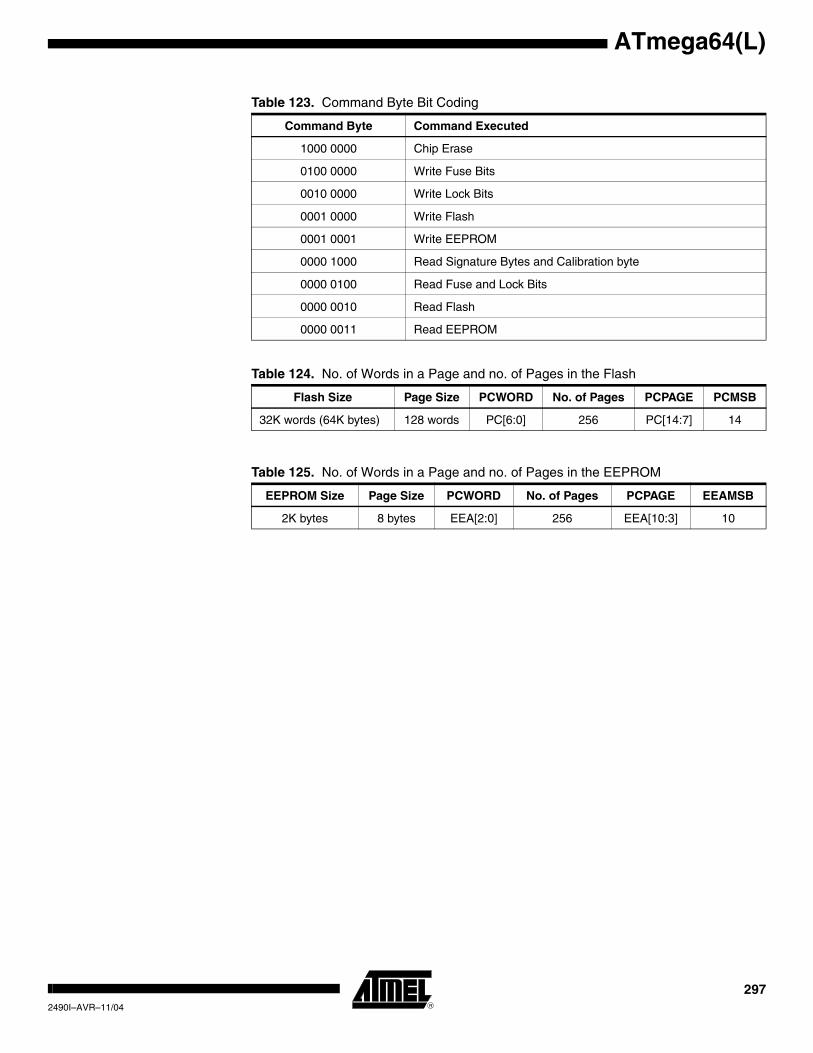
ATmega64(L)
Table 123. Command Byte Bit Coding
Command Byte Command Executed
1000 0000 Chip Erase
0100 0000 Write Fuse Bits
0010 0000 Write Lock Bits
0001 0000 Write Flash
0001 0001 Write EEPROM
0000 1000 Read Signature Bytes and Calibration byte
0000 0100 Read Fuse and Lock Bits
0000 0010 Read Flash
0000 0011 Read EEPROM
Table 124. No. of Words in a Page and no. of Pages in the Flash
Flash Size Page Size PCWORD No. of Pages PCPAGE PCMSB
32K words (64K bytes) 128 words PC[6:0] 256 PC[14:7] 14
Table 125. No. of Words in a Page and no. of Pages in the EEPROM
EEPROM Size Page Size PCWORD No. of Pages PCPAGE EEAMSB
2K bytes 8 bytes EEA[2:0] 256 EEA[10:3] 10
2972490I–AVR–11/04
Parallel Programming
Enter Programming Mode The following algorithm puts the device in Parallel Programming mode:
1. Apply 4.5 - 5.5V between VCC and GND, and wait at least 100 µs.
2. Set RESET to “0” and toggle XTAL1 at least six times.
3. Set the Prog_enable pins listed in Table 121 on page 296 to “0000” and wait at least 100 ns.
4. Apply 11.5 - 12.5V to RESET. Any activity on Prog_enable pins within 100 ns after +12V has been applied to RESET, will cause the device to fail entering Pro-gramming mode.
Note, if External Crystal or External RC configuration is selected, it may not be possibleto apply qualified XTAL1 pulses. In such cases, the following algorithm should befollowed:
1. Set Prog_enable pins listed in Table on page 296 to “0000”.
2. Apply 4.5 - 5.5V between VCC and GND simultaneously as 11.5 - 12.5V is applied to RESET.
3. Wait 100 µs.
4. Re-program the fuses to ensure that External Clock is selected as clock source (CKSEL3:0 = 0b0000) If Lock bits are programmed, a Chip Erase command must be executed before changing the fuses.
5. Exit Programming mode by power the device down or by bringing RESET pin to 0b0.
6. Entering Programming mode with the original algorithm, as described above.
Considerations for Efficient Programming
The loaded command and address are retained in the device during programming. Forefficient programming, the following should be considered.
• The command needs only be loaded once when writing or reading multiple memory locations.
• Skip writing the data value 0xFF, that is the contents of the entire EEPROM (unless the EESAVE Fuse is programmed) and Flash after a Chip Erase.
• Address high byte needs only be loaded before programming or reading a new 256 word window in Flash or 256 byte EEPROM. This consideration also applies to Signature bytes reading.
Chip Erase The Chip Erase will erase the Flash and EEPROM(1) memories plus Lock bits. The Lockbits are not reset until the program memory has been completely erased. The Fuse bitsare not changed. A Chip Erase must be performed before the Flash and/or theEEPROM reprogrammed.Note: 1. The EEPRPOM memory is preserved during chip erase if the EESAVE Fuse is
programmed.
Load Command “Chip Erase”
1. Set XA1, XA0 to “10”. This enables command loading.
2. Set BS1 to “0”.
3. Set DATA to “1000 0000”. This is the command for Chip Erase.
4. Give XTAL1 a positive pulse. This loads the command.
5. Give WR a negative pulse. This starts the Chip Erase. RDY/BSY goes low.
6. Wait until RDY/BSY goes high before loading a new command.
298 ATmega64(L)2490I–AVR–11/04
ATmega64(L)
Programming the Flash The Flash is organized in pages, see Table 123 on page 297. When programming theFlash, the program data is latched into a page buffer. This allows one page of programdata to be programmed simultaneously. The following procedure describes how to pro-gram the entire Flash memory:
A. Load Command “Write Flash”
1. Set XA1, XA0 to “10”. This enables command loading.
2. Set BS1 to “0”.
3. Set DATA to “0001 0000”. This is the command for Write Flash.
4. Give XTAL1 a positive pulse. This loads the command.
B. Load Address Low byte
1. Set XA1, XA0 to “00”. This enables address loading.
2. Set BS1 to “0”. This selects low address.
3. Set DATA = Address low byte (0x00 - 0xFF).
4. Give XTAL1 a positive pulse. This loads the address low byte.
C. Load Data Low Byte
1. Set XA1, XA0 to “01”. This enables data loading.
2. Set DATA = Data low byte (0x00 - 0xFF).
3. Give XTAL1 a positive pulse. This loads the data byte.
D. Load Data High Byte
1. Set BS1 to “1”. This selects high data byte.
2. Set XA1, XA0 to “01”. This enables data loading.
3. Set DATA = Data high byte (0x00 - 0xFF).
4. Give XTAL1 a positive pulse. This loads the data byte.
E. Latch Data
1. Set BS1 to “1”. This selects high data byte.
2. Give PAGEL a positive pulse. This latches the data bytes. (See Figure 140 for signal waveforms).
F. Repeat B through E until the entire buffer is filled or until all data within the page isloaded.
While the lower bits in the address are mapped to words within the page, the higher bitsaddress the pages within the Flash. This is illustrated in Figure 139 on page 300. Notethat if less than eight bits are required to address words in the page (pagesize < 256),the most significant bit(s) in the address low byte are used to address the page whenperforming a Page Write.
G. Load Address High byte
1. Set XA1, XA0 to “00”. This enables address loading.
2. Set BS1 to “1”. This selects high address.
3. Set DATA = Address high byte (0x00 - 0xFF).
4. Give XTAL1 a positive pulse. This loads the address high byte.
H. Program Page
1. Set BS1 = “0”.
2. Give WR a negative pulse. This starts programming of the entire page of data. RDY/BSYgoes low.
2992490I–AVR–11/04
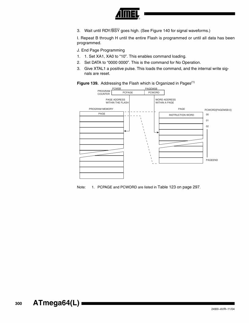
3. Wait until RDY/BSY goes high. (See Figure 140 for signal waveforms.)
I. Repeat B through H until the entire Flash is programmed or until all data has beenprogrammed.
J. End Page Programming
1. 1. Set XA1, XA0 to “10”. This enables command loading.
2. Set DATA to “0000 0000”. This is the command for No Operation.
3. Give XTAL1 a positive pulse. This loads the command, and the internal write sig-nals are reset.
Figure 139. Addressing the Flash which is Organized in Pages(1)
Note: 1. PCPAGE and PCWORD are listed in Table 123 on page 297.
PROGRAM MEMORY
WORD ADDRESSWITHIN A PAGE
PAGE ADDRESSWITHIN THE FLASH
INSTRUCTION WORD
PAGE PCWORD[PAGEMSB:0]:
00
01
02
PAGEEND
PAGE
PCWORDPCPAGE
PCMSB PAGEMSBPROGRAMCOUNTER
300 ATmega64(L)2490I–AVR–11/04
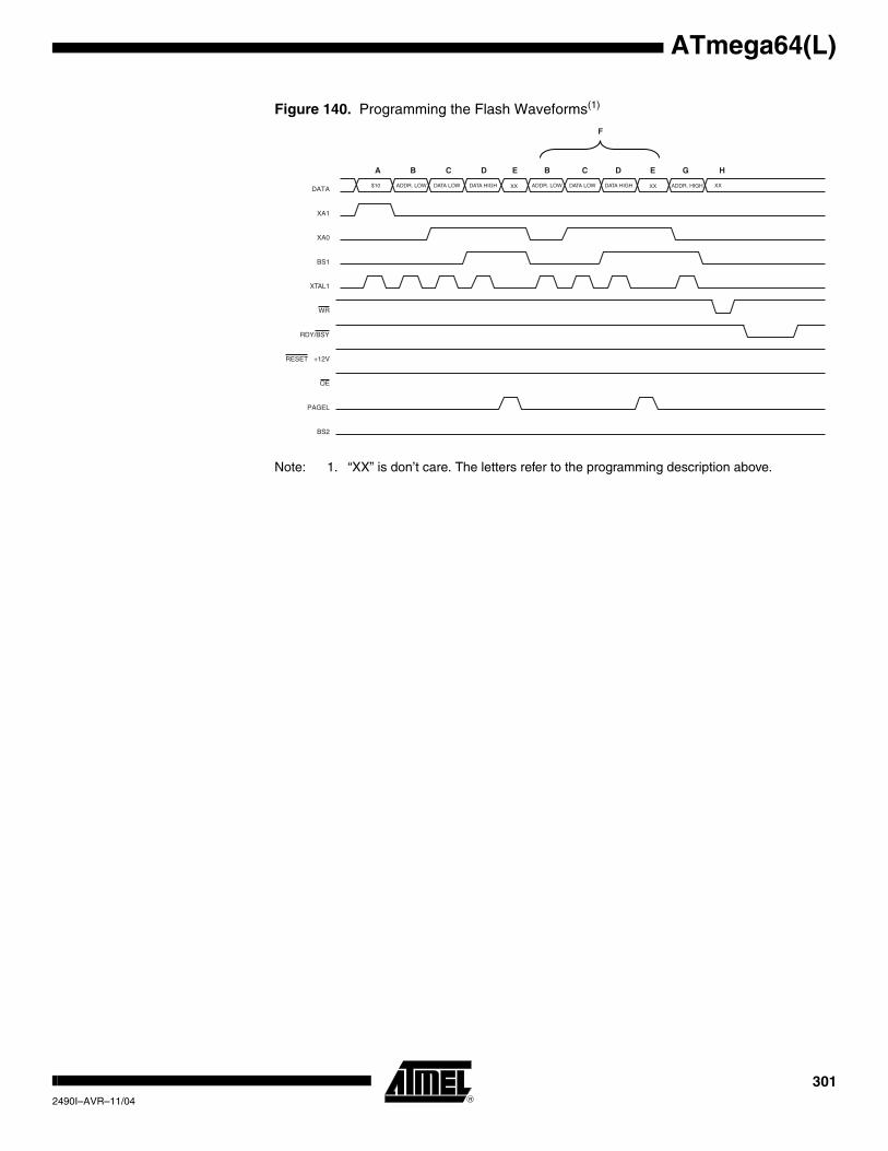
ATmega64(L)
Figure 140. Programming the Flash Waveforms(1)
Note: 1. “XX” is don’t care. The letters refer to the programming description above.
RDY/BSY
WR
OE
RESET +12V
PAGEL
BS2
$10 ADDR. LOW ADDR. HIGHDATADATA LOW DATA HIGH ADDR. LOW DATA LOW DATA HIGH
XA1
XA0
BS1
XTAL1
XX XX XX
A B C D E B C D E G H
F
3012490I–AVR–11/04
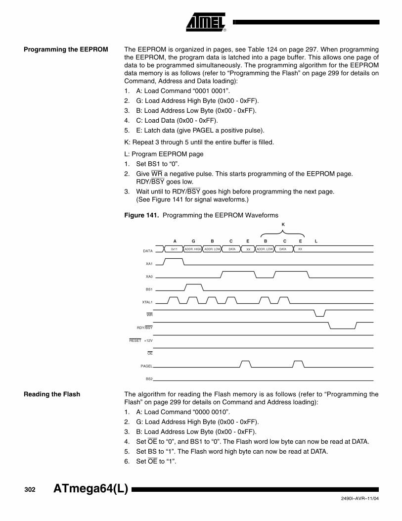
Programming the EEPROM The EEPROM is organized in pages, see Table 124 on page 297. When programmingthe EEPROM, the program data is latched into a page buffer. This allows one page ofdata to be programmed simultaneously. The programming algorithm for the EEPROMdata memory is as follows (refer to “Programming the Flash” on page 299 for details onCommand, Address and Data loading):
1. A: Load Command “0001 0001”.
2. G: Load Address High Byte (0x00 - 0xFF).
3. B: Load Address Low Byte (0x00 - 0xFF).
4. C: Load Data (0x00 - 0xFF).
5. E: Latch data (give PAGEL a positive pulse).
K: Repeat 3 through 5 until the entire buffer is filled.
L: Program EEPROM page
1. Set BS1 to “0”.
2. Give WR a negative pulse. This starts programming of the EEPROM page. RDY/BSY goes low.
3. Wait until to RDY/BSY goes high before programming the next page.(See Figure 141 for signal waveforms.)
Figure 141. Programming the EEPROM Waveforms
Reading the Flash The algorithm for reading the Flash memory is as follows (refer to “Programming theFlash” on page 299 for details on Command and Address loading):
1. A: Load Command “0000 0010”.
2. G: Load Address High Byte (0x00 - 0xFF).
3. B: Load Address Low Byte (0x00 - 0xFF).
4. Set OE to “0”, and BS1 to “0”. The Flash word low byte can now be read at DATA.
5. Set BS to “1”. The Flash word high byte can now be read at DATA.
6. Set OE to “1”.
RDY/BSY
WR
OE
RESET +12V
PAGEL
BS2
0x11 ADDR. HIGHDATA
ADDR. LOW DATA ADDR. LOW DATA XX
XA1
XA0
BS1
XTAL1
XX
A G B C E B C E L
K
302 ATmega64(L)2490I–AVR–11/04
ATmega64(L)
Reading the EEPROM The algorithm for reading the EEPROM memory is as follows (refer to “Programming theFlash” on page 299 for details on Command and Address loading):
1. A: Load Command “0000 0011”.
2. G: Load Address High Byte (0x00 - 0xFF).
3. B: Load Address Low Byte (0x00 - 0xFF).
4. Set OE to “0”, and BS1 to “0”. The EEPROM Data byte can now be read at DATA.
5. Set OE to “1”.
Programming the Fuse Low Bits
The algorithm for programming the Fuse Low bits is as follows (refer to “Programmingthe Flash” on page 299 for details on Command and Data loading):
1. A: Load Command “0100 0000”.
2. C: Load Data Low Byte. Bit n = “0” programs and bit n = “1” erases the Fuse bit.
3. Set BS1 to “0” and BS2 to “0”.
4. Give WR a negative pulse and wait for RDY/BSY to go high.
Programming the Fuse High Bits
The algorithm for programming the Fuse High bits is as follows (refer to “Programmingthe Flash” on page 299 for details on Command and Data loading):
1. A: Load Command “0100 0000”.
2. C: Load Data Low Byte. Bit n = “0” programs and bit n = “1” erases the Fuse bit.
3. Set BS1 to “1” and BS2 to “0”. This selects high data byte.
4. Give WR a negative pulse and wait for RDY/BSY to go high.
5. Set BS1 to “0”. This selects low data byte.
Programming the Extended Fuse Bits
The algorithm for programming the Extended Fuse bits is as follows (refer to “Program-ming the Flash” on page 299 for details on Command and Data loading):
1. A: Load Command “0100 0000”.
2. C: Load Data Low Byte. Bit n = “0” programs and bit n = “1” erases the Fuse bit.
3. Set BS2 to “1” and BS1 to “0”. This selects extended data byte.
4. Give WR a negative pulse and wait for RDY/BSY to go high.
5. Set BS2 to “0”. This selects low data byte.
3032490I–AVR–11/04
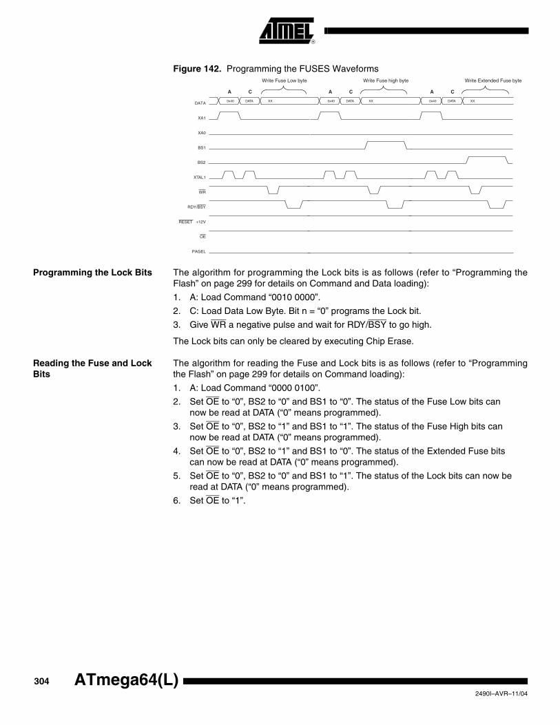
Figure 142. Programming the FUSES Waveforms
Programming the Lock Bits The algorithm for programming the Lock bits is as follows (refer to “Programming theFlash” on page 299 for details on Command and Data loading):
1. A: Load Command “0010 0000”.
2. C: Load Data Low Byte. Bit n = “0” programs the Lock bit.
3. Give WR a negative pulse and wait for RDY/BSY to go high.
The Lock bits can only be cleared by executing Chip Erase.
Reading the Fuse and Lock Bits
The algorithm for reading the Fuse and Lock bits is as follows (refer to “Programmingthe Flash” on page 299 for details on Command loading):
1. A: Load Command “0000 0100”.
2. Set OE to “0”, BS2 to “0” and BS1 to “0”. The status of the Fuse Low bits can now be read at DATA (“0” means programmed).
3. Set OE to “0”, BS2 to “1” and BS1 to “1”. The status of the Fuse High bits can now be read at DATA (“0” means programmed).
4. Set OE to “0”, BS2 to “1” and BS1 to “0”. The status of the Extended Fuse bits can now be read at DATA (“0” means programmed).
5. Set OE to “0”, BS2 to “0” and BS1 to “1”. The status of the Lock bits can now be read at DATA (“0” means programmed).
6. Set OE to “1”.
RDY/BSY
WR
OE
RESET +12V
PAGEL
0x40DATA
DATA XX
XA1
XA0
BS1
XTAL1
A C
0x40 DATA XX
A C
Write Fuse Low byte Write Fuse high byte
0x40 DATA XX
A C
Write Extended Fuse byte
BS2
304 ATmega64(L)2490I–AVR–11/04
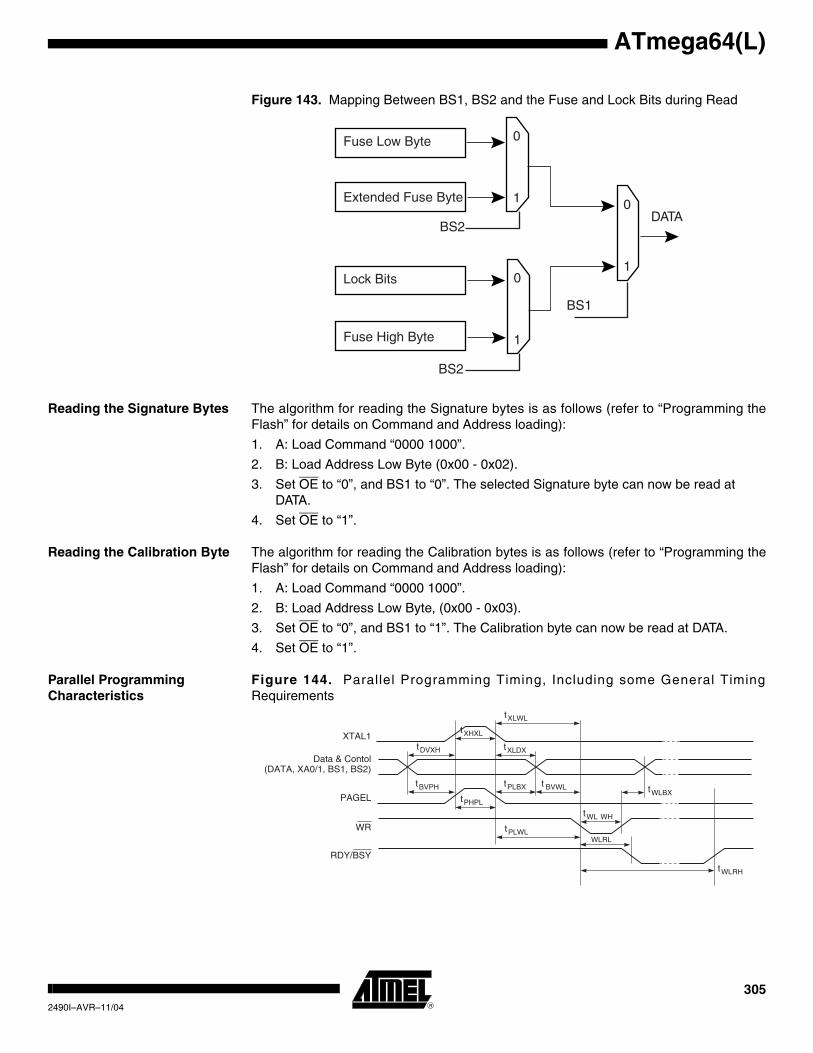
ATmega64(L)
Figure 143. Mapping Between BS1, BS2 and the Fuse and Lock Bits during Read
Reading the Signature Bytes The algorithm for reading the Signature bytes is as follows (refer to “Programming theFlash” for details on Command and Address loading):
1. A: Load Command “0000 1000”.
2. B: Load Address Low Byte (0x00 - 0x02).
3. Set OE to “0”, and BS1 to “0”. The selected Signature byte can now be read at DATA.
4. Set OE to “1”.
Reading the Calibration Byte The algorithm for reading the Calibration bytes is as follows (refer to “Programming theFlash” for details on Command and Address loading):
1. A: Load Command “0000 1000”.
2. B: Load Address Low Byte, (0x00 - 0x03).
3. Set OE to “0”, and BS1 to “1”. The Calibration byte can now be read at DATA.
4. Set OE to “1”.
Parallel Programming Characteristics
Figure 144. Parallel Programming Timing, Including some General TimingRequirements
Lock Bits 0
1
BS2
Fuse High Byte
BS1
DATA
Fuse Low Byte
BS2
Extended Fuse Byte
0
1 0
1
Data & Contol(DATA, XA0/1, BS1, BS2)
XTAL1tXHXL
tWL WH
tDVXH tXLDX
tPLWL
tWLRH
WR
RDY/BSY
PAGEL tPHPL
tPLBXtBVPH
tXLWL
tWLBXt BVWL
WLRL
3052490I–AVR–11/04
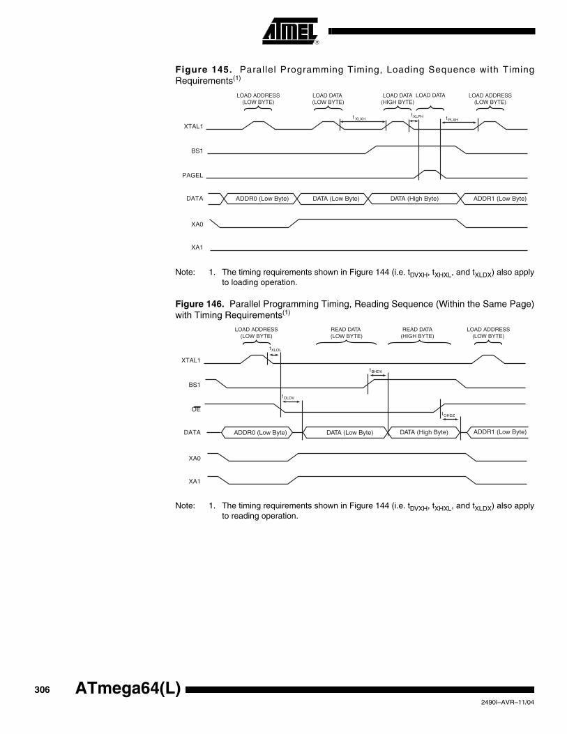
Figure 145. Parallel Programming Timing, Loading Sequence with TimingRequirements(1)
Note: 1. The timing requirements shown in Figure 144 (i.e. tDVXH, tXHXL, and tXLDX) also applyto loading operation.
Figure 146. Parallel Programming Timing, Reading Sequence (Within the Same Page)with Timing Requirements(1)
Note: 1. The timing requirements shown in Figure 144 (i.e. tDVXH, tXHXL, and tXLDX) also applyto reading operation.
XTAL1
PAGEL
tPLXHXLXHt tXLPH
ADDR0 (Low Byte) DATA (Low Byte) DATA (High Byte) ADDR1 (Low Byte)DATA
BS1
XA0
XA1
LOAD ADDRESS(LOW BYTE)
LOAD DATA (LOW BYTE)
LOAD DATA(HIGH BYTE)
LOAD DATA LOAD ADDRESS(LOW BYTE)
XTAL1
OE
ADDR0 (Low Byte) DATA (Low Byte) DATA (High Byte) ADDR1 (Low Byte)DATA
BS1
XA0
XA1
LOAD ADDRESS(LOW BYTE)
READ DATA (LOW BYTE)
READ DATA(HIGH BYTE)
LOAD ADDRESS(LOW BYTE)
tBHDV
tOLDV
tXLOL
tOHDZ
306 ATmega64(L)2490I–AVR–11/04
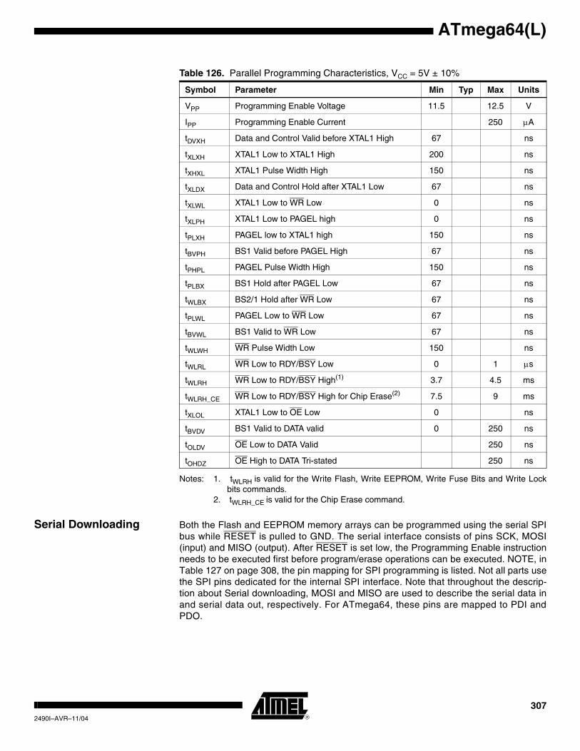
ATmega64(L)
Notes: 1. tWLRH is valid for the Write Flash, Write EEPROM, Write Fuse Bits and Write Lockbits commands.
2. tWLRH_CE is valid for the Chip Erase command.
Serial Downloading Both the Flash and EEPROM memory arrays can be programmed using the serial SPIbus while RESET is pulled to GND. The serial interface consists of pins SCK, MOSI(input) and MISO (output). After RESET is set low, the Programming Enable instructionneeds to be executed first before program/erase operations can be executed. NOTE, inTable 127 on page 308, the pin mapping for SPI programming is listed. Not all parts usethe SPI pins dedicated for the internal SPI interface. Note that throughout the descrip-tion about Serial downloading, MOSI and MISO are used to describe the serial data inand serial data out, respectively. For ATmega64, these pins are mapped to PDI andPDO.
Table 126. Parallel Programming Characteristics, VCC = 5V ± 10%
Symbol Parameter Min Typ Max Units
VPP Programming Enable Voltage 11.5 12.5 V
IPP Programming Enable Current 250 µA
tDVXH Data and Control Valid before XTAL1 High 67 ns
tXLXH XTAL1 Low to XTAL1 High 200 ns
tXHXL XTAL1 Pulse Width High 150 ns
tXLDX Data and Control Hold after XTAL1 Low 67 ns
tXLWL XTAL1 Low to WR Low 0 ns
tXLPH XTAL1 Low to PAGEL high 0 ns
tPLXH PAGEL low to XTAL1 high 150 ns
tBVPH BS1 Valid before PAGEL High 67 ns
tPHPL PAGEL Pulse Width High 150 ns
tPLBX BS1 Hold after PAGEL Low 67 ns
tWLBX BS2/1 Hold after WR Low 67 ns
tPLWL PAGEL Low to WR Low 67 ns
tBVWL BS1 Valid to WR Low 67 ns
tWLWH WR Pulse Width Low 150 ns
tWLRL WR Low to RDY/BSY Low 0 1 µs
tWLRH WR Low to RDY/BSY High(1) 3.7 4.5 ms
tWLRH_CE WR Low to RDY/BSY High for Chip Erase(2) 7.5 9 ms
tXLOL XTAL1 Low to OE Low 0 ns
tBVDV BS1 Valid to DATA valid 0 250 ns
tOLDV OE Low to DATA Valid 250 ns
tOHDZ OE High to DATA Tri-stated 250 ns
3072490I–AVR–11/04
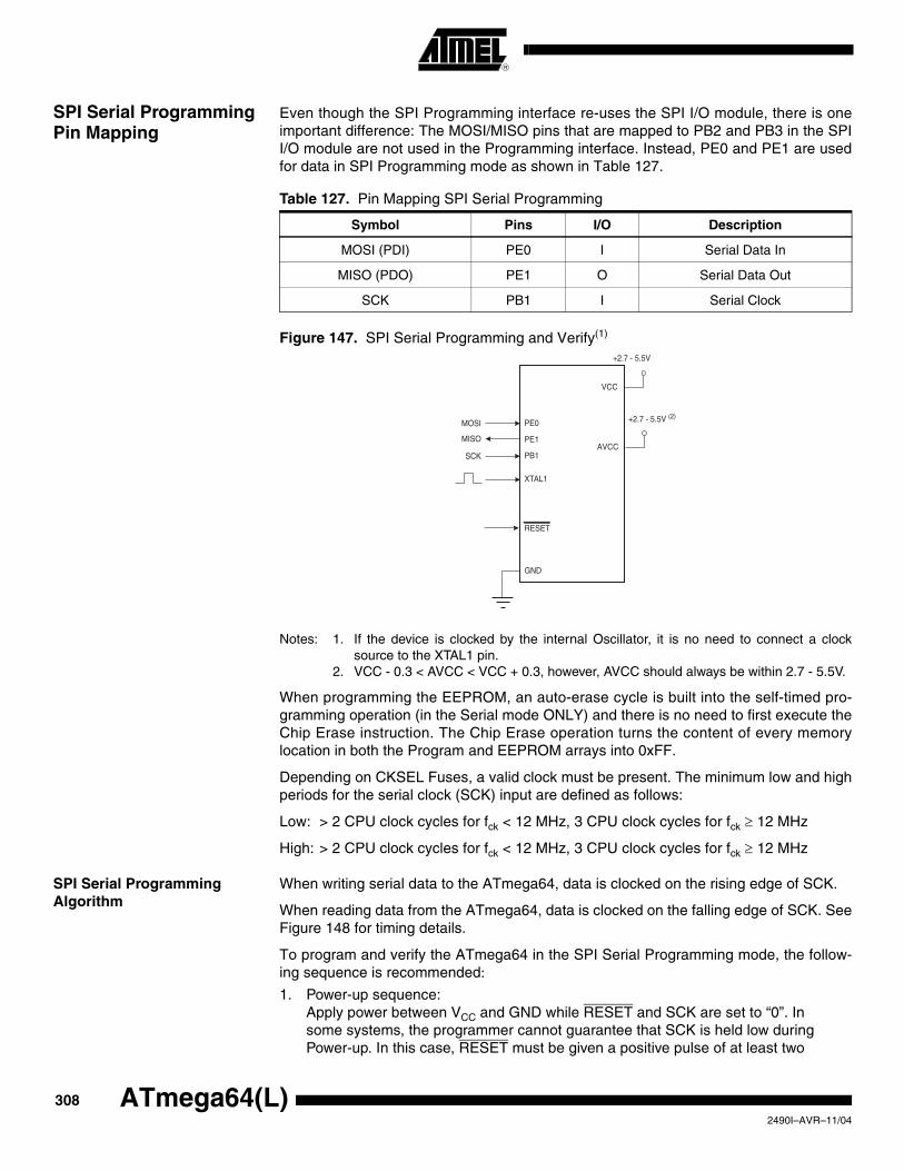
SPI Serial Programming Pin Mapping
Even though the SPI Programming interface re-uses the SPI I/O module, there is oneimportant difference: The MOSI/MISO pins that are mapped to PB2 and PB3 in the SPII/O module are not used in the Programming interface. Instead, PE0 and PE1 are usedfor data in SPI Programming mode as shown in Table 127.
Figure 147. SPI Serial Programming and Verify(1)
Notes: 1. If the device is clocked by the internal Oscillator, it is no need to connect a clocksource to the XTAL1 pin.
2. VCC - 0.3 < AVCC < VCC + 0.3, however, AVCC should always be within 2.7 - 5.5V.
When programming the EEPROM, an auto-erase cycle is built into the self-timed pro-gramming operation (in the Serial mode ONLY) and there is no need to first execute theChip Erase instruction. The Chip Erase operation turns the content of every memorylocation in both the Program and EEPROM arrays into 0xFF.
Depending on CKSEL Fuses, a valid clock must be present. The minimum low and highperiods for the serial clock (SCK) input are defined as follows:
Low: > 2 CPU clock cycles for fck < 12 MHz, 3 CPU clock cycles for fck ≥ 12 MHz
High: > 2 CPU clock cycles for fck < 12 MHz, 3 CPU clock cycles for fck ≥ 12 MHz
SPI Serial Programming Algorithm
When writing serial data to the ATmega64, data is clocked on the rising edge of SCK.
When reading data from the ATmega64, data is clocked on the falling edge of SCK. SeeFigure 148 for timing details.
To program and verify the ATmega64 in the SPI Serial Programming mode, the follow-ing sequence is recommended:1. Power-up sequence:
Apply power between VCC and GND while RESET and SCK are set to “0”. In some systems, the programmer cannot guarantee that SCK is held low during Power-up. In this case, RESET must be given a positive pulse of at least two
Table 127. Pin Mapping SPI Serial Programming
Symbol Pins I/O Description
MOSI (PDI) PE0 I Serial Data In
MISO (PDO) PE1 O Serial Data Out
SCK PB1 I Serial Clock
VCC
GND
XTAL1
SCK
MISO
MOSI
RESET
PE0
PE1
PB1
+2.7 - 5.5V
AVCC
+2.7 - 5.5V (2)
308 ATmega64(L)2490I–AVR–11/04
ATmega64(L)
CPU clock cycles duration after SCK has been set to “0”.As an alternative to using the RESET signal, PEN can be held low during Power-on Reset while SCK is set to “0”. In this case, only the PEN value at Power-on Reset is important. If the programmer cannot guarantee that SCK is held low during Power-up, the PEN method cannot be used. The device must be powered down in order to commence normal operation when using this method.
2. Wait for at least 20 ms and enable SPI Serial Programming by sending the Pro-gramming Enable serial instruction to pin MOSI.
3. The SPI Serial Programming instructions will not work if the communication is out of synchronization. When in sync. the second byte (0x53), will echo back when issuing the third byte of the Programming Enable instruction. Whether the echo is correct or not, all four bytes of the instruction must be transmitted. If the 0x53 did not echo back, give RESET a positive pulse and issue a new Program-ming Enable command.
4. The Flash is programmed one page at a time. The Page size is found in Table 124 on page 297. The memory page is loaded one byte at a time by supplying the 7 LSB of the address and data together with the Load Program Memory Page instruction. To ensure correct loading of the page, the data low byte must be loaded before data high byte is applied for given address. The Program Mem-ory Page is stored by loading the Write Program Memory Page instruction with the 8 MSB of the address. If polling is not used, the user must wait at least tWD_FLASH before issuing the next page. (See Table 128). Accessing the SPI Serial Programming interface before the Flash write operation completes can result in incorrect programming.
5. The EEPROM array is programmed one byte at a time by supplying the address and data together with the appropriate Write instruction. An EEPROM memory location is first automatically erased before new data is written. If polling is not used, the user must wait at least tWD_EEPROM before issuing the next byte. (See Table 128).
6. Any memory location can be verified by using the Read instruction which returns the content at the selected address at serial output MISO.
7. At the end of the programming session, RESET can be set high to commence normal operation.
8. Power-off sequence (if needed):Set RESET to “1”.Turn VCC power off.
Note: If other commands that polling (read) are applied before any write operation (FLASH,EEPROM, Lock bits, Fuses) is completed, may result in incorrect programming.
Data Polling Flash When a page is being programmed into the Flash, reading an address location withinthe page being programmed will give the value 0xFF. At the time the device is ready fora new page, the programmed value will read correctly. This is used to determine whenthe next page can be written. Note that the entire page is written simultaneously and anyaddress within the page can be used for polling. Data polling of the Flash will not workfor the value 0xFF, so when programming this value, the user will have to wait for atleast tWD_FLASH before programming the next page. As a chip -erased device contains0xFF in all locations, programming of addresses that are meant to contain 0xFF, can beskipped. See Table 128 for tWD_FLASH value.
3092490I–AVR–11/04
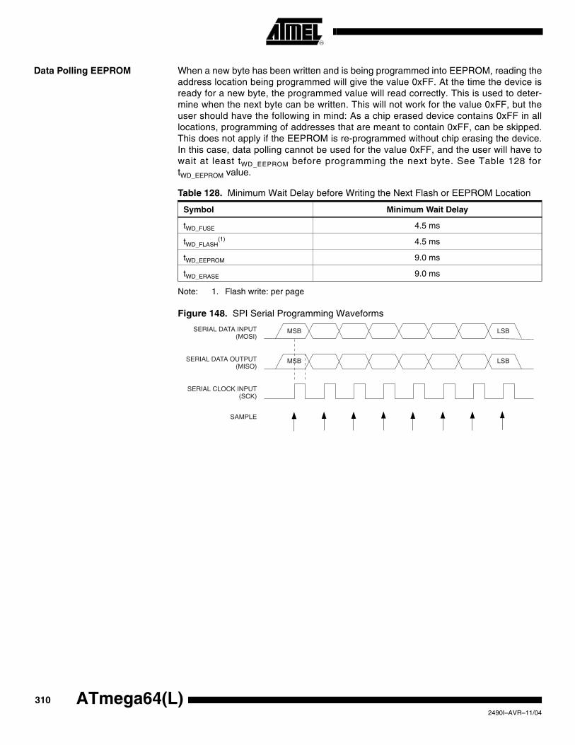
Data Polling EEPROM When a new byte has been written and is being programmed into EEPROM, reading theaddress location being programmed will give the value 0xFF. At the time the device isready for a new byte, the programmed value will read correctly. This is used to deter-mine when the next byte can be written. This will not work for the value 0xFF, but theuser should have the following in mind: As a chip erased device contains 0xFF in alllocations, programming of addresses that are meant to contain 0xFF, can be skipped.This does not apply if the EEPROM is re-programmed without chip erasing the device.In this case, data polling cannot be used for the value 0xFF, and the user will have towait at least tWD_EEPROM before programming the next byte. See Table 128 fortWD_EEPROM value.
Note: 1. Flash write: per page
Figure 148. SPI Serial Programming Waveforms
Table 128. Minimum Wait Delay before Writing the Next Flash or EEPROM Location
Symbol Minimum Wait Delay
tWD_FUSE 4.5 ms
tWD_FLASH(1) 4.5 ms
tWD_EEPROM 9.0 ms
tWD_ERASE 9.0 ms
MSB
MSB
LSB
LSB
SERIAL CLOCK INPUT(SCK)
SERIAL DATA INPUT (MOSI)
(MISO)
SAMPLE
SERIAL DATA OUTPUT
310 ATmega64(L)2490I–AVR–11/04
ATmega64(L)
Table 129. SPI Serial Programming Instruction Set
Instruction
Instruction Format
OperationByte 1 Byte 2 Byte 3 Byte4
Programming Enable 1010 1100 0101 0011 xxxx xxxx xxxx xxxx Enable SPI Serial Programming after RESET goes low.
Chip Erase 1010 1100 100x xxxx xxxx xxxx xxxx xxxx Chip Erase EEPROM and Flash.
Read Program Memory 0010 H000 xaaa aaaa bbbb bbbb oooo oooo Read H (high or low) data o from Program memory at word address a:b.
Load Program Memory Page
0100 H000 xxxx xxxx xbbb bbbb iiii iiii Write H (high or low) data i to Program Memory page at word address b. Data low byte must be loaded before data high byte is applied within the same address.
Write Program Memory Page
0100 1100 xaaa aaaa bxxx xxxx xxxx xxxx Write Program Memory Page at address a:b.
Read EEPROM Memory 1010 0000 xxxx xaaa bbbb bbbb oooo oooo Read data o from EEPROM memory at address a:b.
Write EEPROM Memory 1100 0000 xxxx xaaa bbbb bbbb iiii iiii Write data i to EEPROM memory at address a:b.
Read Lock Bits 0101 1000 0000 0000 xxxx xxxx xxoo oooo Read Lock bits. “0” = programmed, “1” = unprogrammed. See Table 115 on page 291 for details.
Write Lock Bits 1010 1100 111x xxxx xxxx xxxx 11ii iiii Write Lock bits. Set bits = “0” to program Lock bits. See Table 115 on page 291 for details.
Read Signature Byte 0011 0000 xxxx xxxx xxxx xxbb oooo oooo Read Signature Byte o at address b.
Write Fuse Bits 1010 1100 1010 0000 xxxx xxxx iiii iiii Set bits = “0” to program, “1” to unprogram. See Table 119 on page 293 for details.
Write Fuse High Bits 1010 1100 1010 1000 xxxx xxxx iiii iiii Set bits = “0” to program, “1” to unprogram. See Table 118 on page 293 for details.
Write Extended Fuse Bits 1010 1100 1010 0100 xxxx xxxx xxxx xxii Set bits = “0” to program, “1” to unprogram. See Table 119 on page 293 for details.
Read Fuse Bits 0101 0000 0000 0000 xxxx xxxx oooo oooo Read Fuse bits. “0” = programmed, “1” = unprogrammed. See Table 119 on page 293 for details.
3112490I–AVR–11/04
Note: a = address high bits, b = address low bits, H = 0 - Low byte, 1 - High Byte, o = data out, i = data in, x = don’t care
SPI Serial Programming Characteristics
For characteristics of the SPI module, see “SPI Timing Characteristics” on page 332.
Read Extendend Fuse Bits
0101 0000 0000 1000 xxxx xxxx oooo oooo Read Extended Fuse bits. “0” = pro-grammed, “1” = unprogrammed. See Table 119 on page 293 for details.
Read Fuse High Bits 0101 1000 0000 1000 xxxx xxxx oooo oooo Read Fuse high bits. “0” = pro-grammed, “1” = unprogrammed. See Table 118 on page 293 for details.
Read Calibration Byte 0011 1000 00xx xxxx 0000 00bb oooo oooo Read Calibration Byte o at address b.
Table 129. SPI Serial Programming Instruction Set (Continued)
Instruction
Instruction Format
OperationByte 1 Byte 2 Byte 3 Byte4
312 ATmega64(L)2490I–AVR–11/04
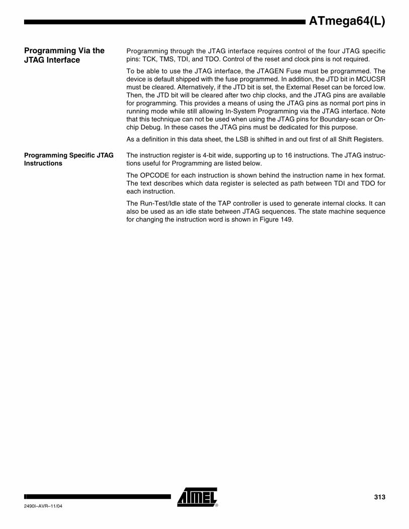
ATmega64(L)
Programming Via the JTAG Interface
Programming through the JTAG interface requires control of the four JTAG specificpins: TCK, TMS, TDI, and TDO. Control of the reset and clock pins is not required.
To be able to use the JTAG interface, the JTAGEN Fuse must be programmed. Thedevice is default shipped with the fuse programmed. In addition, the JTD bit in MCUCSRmust be cleared. Alternatively, if the JTD bit is set, the External Reset can be forced low.Then, the JTD bit will be cleared after two chip clocks, and the JTAG pins are availablefor programming. This provides a means of using the JTAG pins as normal port pins inrunning mode while still allowing In-System Programming via the JTAG interface. Notethat this technique can not be used when using the JTAG pins for Boundary-scan or On-chip Debug. In these cases the JTAG pins must be dedicated for this purpose.
As a definition in this data sheet, the LSB is shifted in and out first of all Shift Registers.
Programming Specific JTAG Instructions
The instruction register is 4-bit wide, supporting up to 16 instructions. The JTAG instruc-tions useful for Programming are listed below.
The OPCODE for each instruction is shown behind the instruction name in hex format.The text describes which data register is selected as path between TDI and TDO foreach instruction.
The Run-Test/Idle state of the TAP controller is used to generate internal clocks. It canalso be used as an idle state between JTAG sequences. The state machine sequencefor changing the instruction word is shown in Figure 149.
3132490I–AVR–11/04
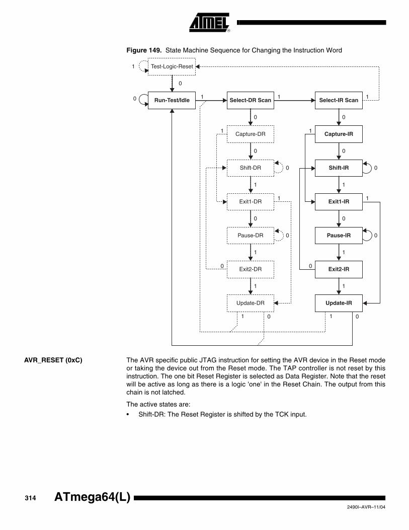
Figure 149. State Machine Sequence for Changing the Instruction Word
AVR_RESET (0xC) The AVR specific public JTAG instruction for setting the AVR device in the Reset modeor taking the device out from the Reset mode. The TAP controller is not reset by thisinstruction. The one bit Reset Register is selected as Data Register. Note that the resetwill be active as long as there is a logic 'one' in the Reset Chain. The output from thischain is not latched.
The active states are:
• Shift-DR: The Reset Register is shifted by the TCK input.
Test-Logic-Reset
Run-Test/Idle
Shift-DR
Exit1-DR
Pause-DR
Exit2-DR
Update-DR
Select-IR Scan
Capture-IR
Shift-IR
Exit1-IR
Pause-IR
Exit2-IR
Update-IR
Select-DR Scan
Capture-DR
0
1
0 1 1 1
0 0
0 0
1 1
1 0
1
1
0
1
0
0
1 0
1
1
0
1
0
0
00
11
314 ATmega64(L)2490I–AVR–11/04
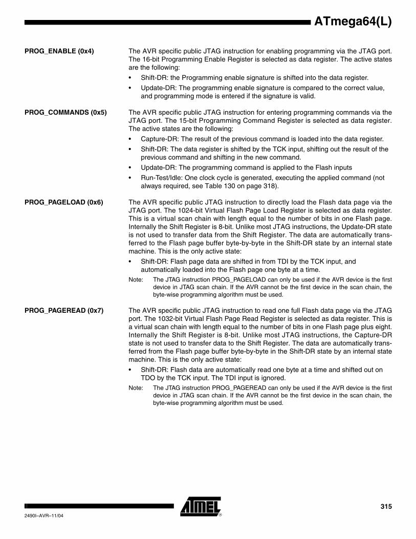
ATmega64(L)
PROG_ENABLE (0x4) The AVR specific public JTAG instruction for enabling programming via the JTAG port.The 16-bit Programming Enable Register is selected as data register. The active statesare the following:
• Shift-DR: the Programming enable signature is shifted into the data register.
• Update-DR: The programming enable signature is compared to the correct value, and programming mode is entered if the signature is valid.
PROG_COMMANDS (0x5) The AVR specific public JTAG instruction for entering programming commands via theJTAG port. The 15-bit Programming Command Register is selected as data register.The active states are the following:
• Capture-DR: The result of the previous command is loaded into the data register.
• Shift-DR: The data register is shifted by the TCK input, shifting out the result of the previous command and shifting in the new command.
• Update-DR: The programming command is applied to the Flash inputs
• Run-Test/Idle: One clock cycle is generated, executing the applied command (not always required, see Table 130 on page 318).
PROG_PAGELOAD (0x6) The AVR specific public JTAG instruction to directly load the Flash data page via theJTAG port. The 1024-bit Virtual Flash Page Load Register is selected as data register.This is a virtual scan chain with length equal to the number of bits in one Flash page.Internally the Shift Register is 8-bit. Unlike most JTAG instructions, the Update-DR stateis not used to transfer data from the Shift Register. The data are automatically trans-ferred to the Flash page buffer byte-by-byte in the Shift-DR state by an internal statemachine. This is the only active state:
• Shift-DR: Flash page data are shifted in from TDI by the TCK input, and automatically loaded into the Flash page one byte at a time.
Note: The JTAG instruction PROG_PAGELOAD can only be used if the AVR device is the firstdevice in JTAG scan chain. If the AVR cannot be the first device in the scan chain, thebyte-wise programming algorithm must be used.
PROG_PAGEREAD (0x7) The AVR specific public JTAG instruction to read one full Flash data page via the JTAGport. The 1032-bit Virtual Flash Page Read Register is selected as data register. This isa virtual scan chain with length equal to the number of bits in one Flash page plus eight.Internally the Shift Register is 8-bit. Unlike most JTAG instructions, the Capture-DRstate is not used to transfer data to the Shift Register. The data are automatically trans-ferred from the Flash page buffer byte-by-byte in the Shift-DR state by an internal statemachine. This is the only active state:
• Shift-DR: Flash data are automatically read one byte at a time and shifted out on TDO by the TCK input. The TDI input is ignored.
Note: The JTAG instruction PROG_PAGEREAD can only be used if the AVR device is the firstdevice in JTAG scan chain. If the AVR cannot be the first device in the scan chain, thebyte-wise programming algorithm must be used.
3152490I–AVR–11/04
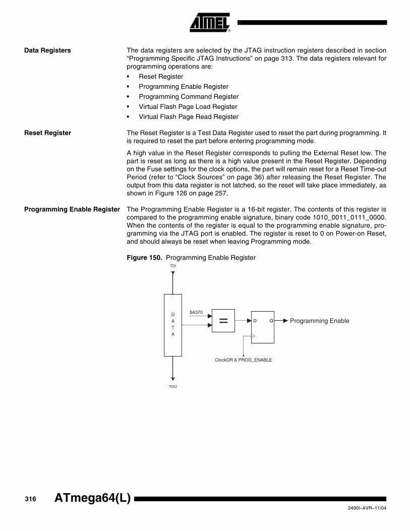
Data Registers The data registers are selected by the JTAG instruction registers described in section“Programming Specific JTAG Instructions” on page 313. The data registers relevant forprogramming operations are:
• Reset Register
• Programming Enable Register
• Programming Command Register
• Virtual Flash Page Load Register
• Virtual Flash Page Read Register
Reset Register The Reset Register is a Test Data Register used to reset the part during programming. Itis required to reset the part before entering programming mode.
A high value in the Reset Register corresponds to pulling the External Reset low. Thepart is reset as long as there is a high value present in the Reset Register. Dependingon the Fuse settings for the clock options, the part will remain reset for a Reset Time-outPeriod (refer to “Clock Sources” on page 36) after releasing the Reset Register. Theoutput from this data register is not latched, so the reset will take place immediately, asshown in Figure 126 on page 257.
Programming Enable Register The Programming Enable Register is a 16-bit register. The contents of this register iscompared to the programming enable signature, binary code 1010_0011_0111_0000.When the contents of the register is equal to the programming enable signature, pro-gramming via the JTAG port is enabled. The register is reset to 0 on Power-on Reset,and should always be reset when leaving Programming mode.
Figure 150. Programming Enable RegisterTDI
TDO
DATA
= D Q
ClockDR & PROG_ENABLE
Programming Enable$A370
316 ATmega64(L)2490I–AVR–11/04
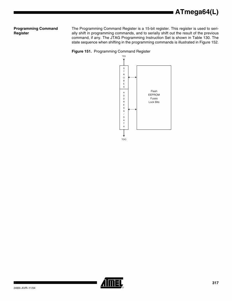
ATmega64(L)
Programming Command Register
The Programming Command Register is a 15-bit register. This register is used to seri-ally shift in programming commands, and to serially shift out the result of the previouscommand, if any. The JTAG Programming Instruction Set is shown in Table 130. Thestate sequence when shifting in the programming commands is illustrated in Figure 152.
Figure 151. Programming Command RegisterTDI
TDO
STROBES
ADDRESS/DATA
FlashEEPROM
FusesLock Bits
3172490I–AVR–11/04
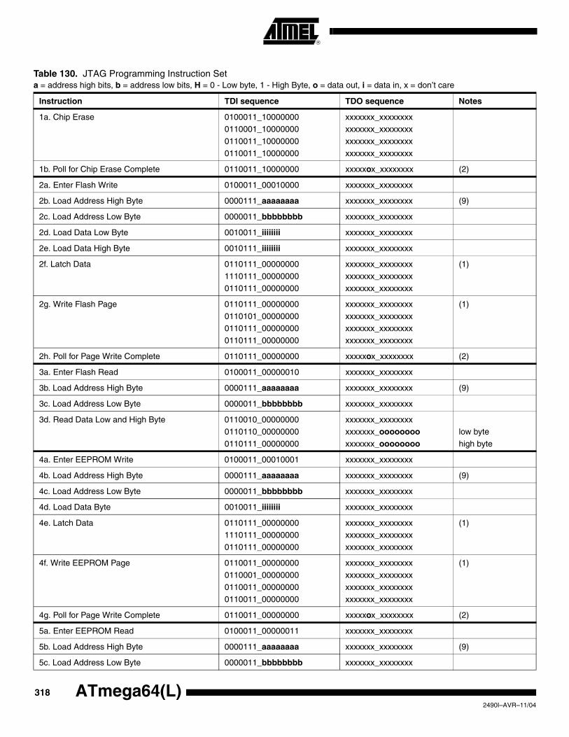
Table 130. JTAG Programming Instruction Set a = address high bits, b = address low bits, H = 0 - Low byte, 1 - High Byte, o = data out, i = data in, x = don’t care
Instruction TDI sequence TDO sequence Notes
1a. Chip Erase 0100011_100000000110001_10000000
0110011_10000000
0110011_10000000
xxxxxxx_xxxxxxxxxxxxxxx_xxxxxxxx
xxxxxxx_xxxxxxxx
xxxxxxx_xxxxxxxx
1b. Poll for Chip Erase Complete 0110011_10000000 xxxxxox_xxxxxxxx (2)
2a. Enter Flash Write 0100011_00010000 xxxxxxx_xxxxxxxx
2b. Load Address High Byte 0000111_aaaaaaaa xxxxxxx_xxxxxxxx (9)
2c. Load Address Low Byte 0000011_bbbbbbbb xxxxxxx_xxxxxxxx
2d. Load Data Low Byte 0010011_iiiiiiii xxxxxxx_xxxxxxxx
2e. Load Data High Byte 0010111_iiiiiiii xxxxxxx_xxxxxxxx
2f. Latch Data 0110111_00000000
1110111_00000000
0110111_00000000
xxxxxxx_xxxxxxxx
xxxxxxx_xxxxxxxx
xxxxxxx_xxxxxxxx
(1)
2g. Write Flash Page 0110111_00000000
0110101_000000000110111_00000000
0110111_00000000
xxxxxxx_xxxxxxxx
xxxxxxx_xxxxxxxxxxxxxxx_xxxxxxxx
xxxxxxx_xxxxxxxx
(1)
2h. Poll for Page Write Complete 0110111_00000000 xxxxxox_xxxxxxxx (2)
3a. Enter Flash Read 0100011_00000010 xxxxxxx_xxxxxxxx
3b. Load Address High Byte 0000111_aaaaaaaa xxxxxxx_xxxxxxxx (9)
3c. Load Address Low Byte 0000011_bbbbbbbb xxxxxxx_xxxxxxxx
3d. Read Data Low and High Byte 0110010_000000000110110_00000000
0110111_00000000
xxxxxxx_xxxxxxxxxxxxxxx_ooooooooxxxxxxx_oooooooo
low byte
high byte
4a. Enter EEPROM Write 0100011_00010001 xxxxxxx_xxxxxxxx
4b. Load Address High Byte 0000111_aaaaaaaa xxxxxxx_xxxxxxxx (9)
4c. Load Address Low Byte 0000011_bbbbbbbb xxxxxxx_xxxxxxxx
4d. Load Data Byte 0010011_iiiiiiii xxxxxxx_xxxxxxxx
4e. Latch Data 0110111_000000001110111_00000000
0110111_00000000
xxxxxxx_xxxxxxxxxxxxxxx_xxxxxxxx
xxxxxxx_xxxxxxxx
(1)
4f. Write EEPROM Page 0110011_00000000
0110001_00000000
0110011_00000000
0110011_00000000
xxxxxxx_xxxxxxxx
xxxxxxx_xxxxxxxx
xxxxxxx_xxxxxxxx
xxxxxxx_xxxxxxxx
(1)
4g. Poll for Page Write Complete 0110011_00000000 xxxxxox_xxxxxxxx (2)
5a. Enter EEPROM Read 0100011_00000011 xxxxxxx_xxxxxxxx
5b. Load Address High Byte 0000111_aaaaaaaa xxxxxxx_xxxxxxxx (9)
5c. Load Address Low Byte 0000011_bbbbbbbb xxxxxxx_xxxxxxxx
318 ATmega64(L)2490I–AVR–11/04
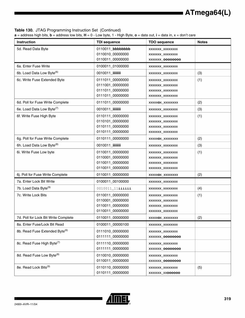
ATmega64(L)
5d. Read Data Byte 0110011_bbbbbbbb0110010_000000000110011_00000000
xxxxxxx_xxxxxxxx
xxxxxxx_xxxxxxxxxxxxxxx_oooooooo
6a. Enter Fuse Write 0100011_01000000 xxxxxxx_xxxxxxxx
6b. Load Data Low Byte(6) 0010011_iiiiiiii xxxxxxx_xxxxxxxx (3)
6c. Write Fuse Extended Byte 0111011_000000000111001_00000000
0111011_00000000
0111011_00000000
xxxxxxx_xxxxxxxxxxxxxxx_xxxxxxxx
xxxxxxx_xxxxxxxx
xxxxxxx_xxxxxxxx
(1)
6d. Poll for Fuse Write Complete 0111011_00000000 xxxxxox_xxxxxxxx (2)
6e. Load Data Low Byte(7) 0010011_iiiiiiii xxxxxxx_xxxxxxxx (3)
6f. Write Fuse High Byte 0110111_000000000110101_00000000
0110111_00000000
0110111_00000000
xxxxxxx_xxxxxxxxxxxxxxx_xxxxxxxx
xxxxxxx_xxxxxxxx
xxxxxxx_xxxxxxxx
(1)
6g. Poll for Fuse Write Complete 0110111_00000000 xxxxxox_xxxxxxxx (2)
6h. Load Data Low Byte(8) 0010011_iiiiiiii xxxxxxx_xxxxxxxx (3)
6i. Write Fuse Low byte 0110011_000000000110001_00000000
0110011_00000000
0110011_00000000
xxxxxxx_xxxxxxxxxxxxxxx_xxxxxxxx
xxxxxxx_xxxxxxxx
xxxxxxx_xxxxxxxx
(1)
6j. Poll for Fuse Write Complete 0110011_00000000 xxxxxox_xxxxxxxx (2)
7a. Enter Lock Bit Write 0100011_00100000 xxxxxxx_xxxxxxxx
7b. Load Data Byte(9) 0010011_11iiiiii xxxxxxx_xxxxxxxx (4)
7c. Write Lock Bits 0110011_00000000
0110001_000000000110011_00000000
0110011_00000000
xxxxxxx_xxxxxxxx
xxxxxxx_xxxxxxxxxxxxxxx_xxxxxxxx
xxxxxxx_xxxxxxxx
(1)
7d. Poll for Lock Bit Write Complete 0110011_00000000 xxxxxox_xxxxxxxx (2)
8a. Enter Fuse/Lock Bit Read 0100011_00000100 xxxxxxx_xxxxxxxx
8b. Read Fuse Extended Byte(6) 0111010_00000000
0111111_00000000
xxxxxxx_xxxxxxxx
xxxxxxx_oooooooo
8c. Read Fuse High Byte(7) 0111110_00000000
0111111_00000000
xxxxxxx_xxxxxxxx
xxxxxxx_oooooooo
8d. Read Fuse Low Byte(8) 0110010_00000000
0110011_00000000
xxxxxxx_xxxxxxxx
xxxxxxx_oooooooo
8e. Read Lock Bits(9) 0110110_00000000
0110111_00000000
xxxxxxx_xxxxxxxx
xxxxxxx_xxoooooo(5)
Table 130. JTAG Programming Instruction Set (Continued)a = address high bits, b = address low bits, H = 0 - Low byte, 1 - High Byte, o = data out, i = data in, x = don’t care
Instruction TDI sequence TDO sequence Notes
3192490I–AVR–11/04
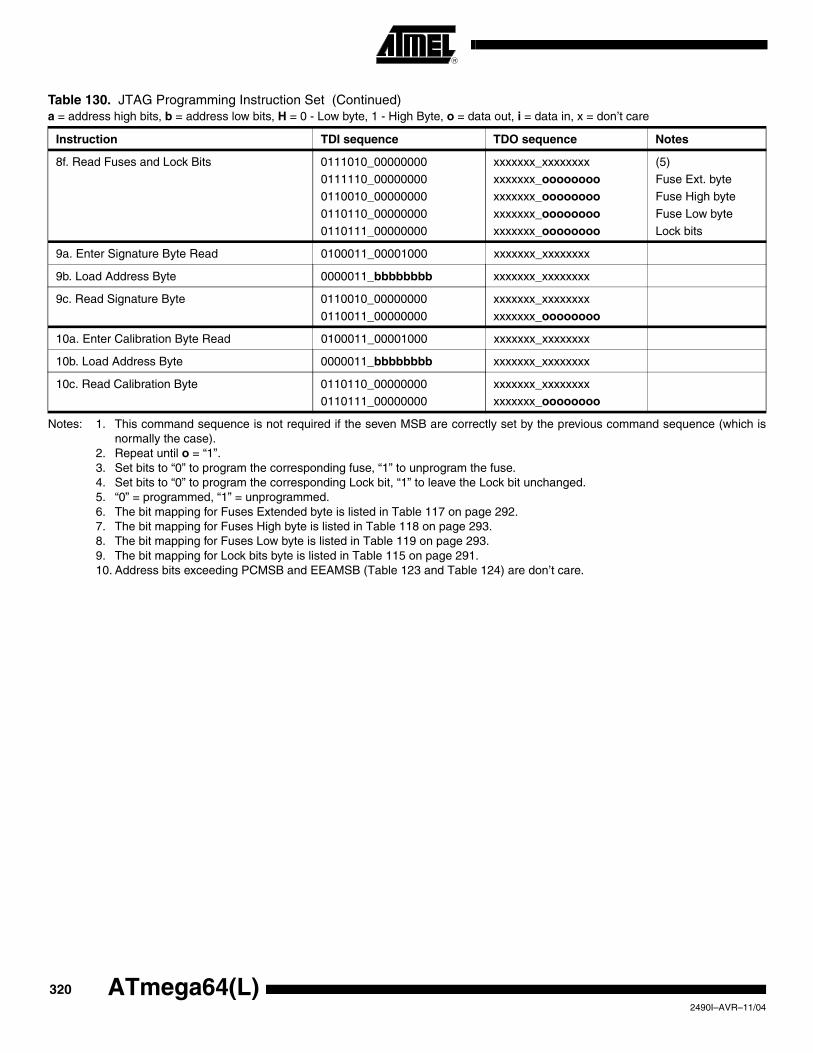
Notes: 1. This command sequence is not required if the seven MSB are correctly set by the previous command sequence (which isnormally the case).
2. Repeat until o = “1”.3. Set bits to “0” to program the corresponding fuse, “1” to unprogram the fuse.4. Set bits to “0” to program the corresponding Lock bit, “1” to leave the Lock bit unchanged.5. “0” = programmed, “1” = unprogrammed.6. The bit mapping for Fuses Extended byte is listed in Table 117 on page 292.7. The bit mapping for Fuses High byte is listed in Table 118 on page 293.8. The bit mapping for Fuses Low byte is listed in Table 119 on page 293.9. The bit mapping for Lock bits byte is listed in Table 115 on page 291.10. Address bits exceeding PCMSB and EEAMSB (Table 123 and Table 124) are don’t care.
8f. Read Fuses and Lock Bits 0111010_00000000
0111110_000000000110010_00000000
0110110_00000000
0110111_00000000
xxxxxxx_xxxxxxxx
xxxxxxx_ooooooooxxxxxxx_ooooooooxxxxxxx_ooooooooxxxxxxx_oooooooo
(5)
Fuse Ext. byteFuse High byte
Fuse Low byte
Lock bits
9a. Enter Signature Byte Read 0100011_00001000 xxxxxxx_xxxxxxxx
9b. Load Address Byte 0000011_bbbbbbbb xxxxxxx_xxxxxxxx
9c. Read Signature Byte 0110010_00000000
0110011_00000000
xxxxxxx_xxxxxxxx
xxxxxxx_oooooooo
10a. Enter Calibration Byte Read 0100011_00001000 xxxxxxx_xxxxxxxx
10b. Load Address Byte 0000011_bbbbbbbb xxxxxxx_xxxxxxxx
10c. Read Calibration Byte 0110110_000000000110111_00000000
xxxxxxx_xxxxxxxxxxxxxxx_oooooooo
Table 130. JTAG Programming Instruction Set (Continued)a = address high bits, b = address low bits, H = 0 - Low byte, 1 - High Byte, o = data out, i = data in, x = don’t care
Instruction TDI sequence TDO sequence Notes
320 ATmega64(L)2490I–AVR–11/04
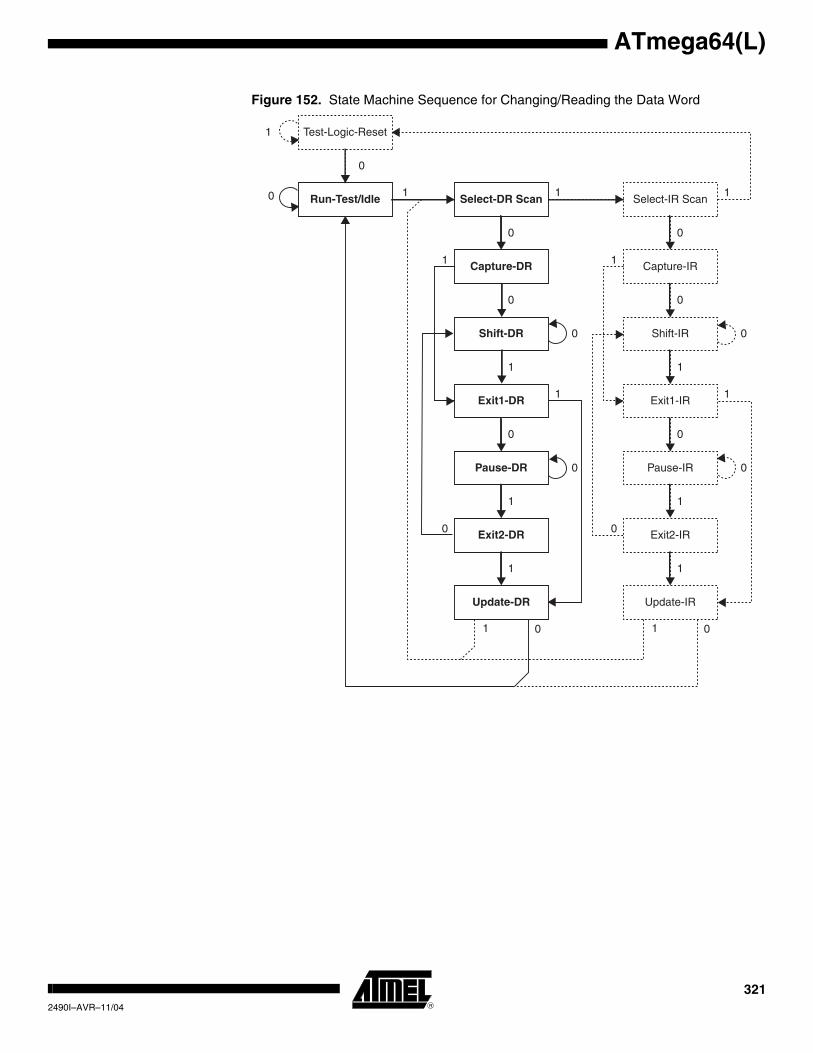
ATmega64(L)
Figure 152. State Machine Sequence for Changing/Reading the Data Word
Test-Logic-Reset
Run-Test/Idle
Shift-DR
Exit1-DR
Pause-DR
Exit2-DR
Update-DR
Select-IR Scan
Capture-IR
Shift-IR
Exit1-IR
Pause-IR
Exit2-IR
Update-IR
Select-DR Scan
Capture-DR
0
1
0 1 1 1
0 0
0 0
1 1
1 0
1
1
0
1
0
0
1 0
1
1
0
1
0
0
00
11
3212490I–AVR–11/04

Virtual Flash Page Load Register
The Virtual Flash Page Load Register is a virtual scan chain with length equal to thenumber of bits in one Flash page. Internally the Shift Register is 8-bit, and the data areautomatically transferred to the Flash page buffer byte-by-byte. Shift in all instructionwords in the page, starting with the LSB of the first instruction in the page and endingwith the MSB of the last instruction in the page. This provides an efficient way to load theentire Flash page buffer before executing Page Write.
Figure 153. Virtual Flash Page Load Register
Virtual Flash Page Read Register
The Virtual Flash Page Read Register is a virtual scan chain with length equal to thenumber of bits in one Flash page plus eight. Internally the Shift Register is 8-bit, and thedata are automatically transferred from the Flash data page byte-by-byte. The first eightcycles are used to transfer the first byte to the internal Shift Register, and the bits thatare shifted out during these eight cycles should be ignored. Following this initialization,data are shifted out starting with the LSB of the first instruction in the page and endingwith the MSB of the last instruction in the page. This provides an efficient way to readone full Flash page to verify programming.
TDI
TDO
DATA
FlashEEPROM
FusesLock Bits
STROBES
ADDRESS
StateMachine
322 ATmega64(L)2490I–AVR–11/04
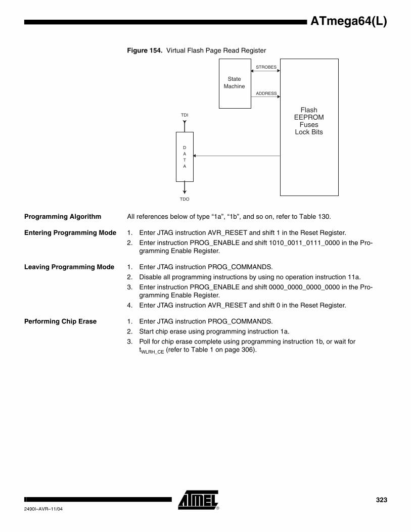
ATmega64(L)
Figure 154. Virtual Flash Page Read Register
Programming Algorithm All references below of type “1a”, “1b”, and so on, refer to Table 130.
Entering Programming Mode 1. Enter JTAG instruction AVR_RESET and shift 1 in the Reset Register.
2. Enter instruction PROG_ENABLE and shift 1010_0011_0111_0000 in the Pro-gramming Enable Register.
Leaving Programming Mode 1. Enter JTAG instruction PROG_COMMANDS.
2. Disable all programming instructions by using no operation instruction 11a.
3. Enter instruction PROG_ENABLE and shift 0000_0000_0000_0000 in the Pro-gramming Enable Register.
4. Enter JTAG instruction AVR_RESET and shift 0 in the Reset Register.
Performing Chip Erase 1. Enter JTAG instruction PROG_COMMANDS.
2. Start chip erase using programming instruction 1a.
3. Poll for chip erase complete using programming instruction 1b, or wait for tWLRH_CE (refer to Table 1 on page 306).
TDI
TDO
DATA
FlashEEPROM
FusesLock Bits
STROBES
ADDRESS
StateMachine
3232490I–AVR–11/04
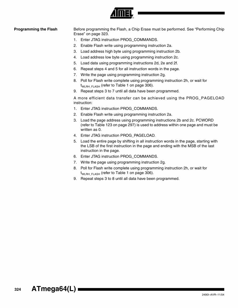
Programming the Flash Before programming the Flash, a Chip Erase must be performed. See “Performing ChipErase” on page 323.
1. Enter JTAG instruction PROG_COMMANDS.
2. Enable Flash write using programming instruction 2a.
3. Load address high byte using programming instruction 2b.
4. Load address low byte using programming instruction 2c.
5. Load data using programming instructions 2d, 2e and 2f.
6. Repeat steps 4 and 5 for all instruction words in the page.
7. Write the page using programming instruction 2g.
8. Poll for Flash write complete using programming instruction 2h, or wait for tWLRH_FLASH (refer to Table 1 on page 306).
9. Repeat steps 3 to 7 until all data have been programmed.
A more efficient data transfer can be achieved using the PROG_PAGELOADinstruction:
1. Enter JTAG instruction PROG_COMMANDS.
2. Enable Flash write using programming instruction 2a.
3. Load the page address using programming instructions 2b and 2c. PCWORD (refer to Table 123 on page 297) is used to address within one page and must be written as 0.
4. Enter JTAG instruction PROG_PAGELOAD.
5. Load the entire page by shifting in all instruction words in the page, starting with the LSB of the first instruction in the page and ending with the MSB of the last instruction in the page.
6. Enter JTAG instruction PROG_COMMANDS.
7. Write the page using programming instruction 2g.
8. Poll for Flash write complete using programming instruction 2h, or wait for tWLRH_FLASH (refer to Table 1 on page 306).
9. Repeat steps 3 to 8 until all data have been programmed.
324 ATmega64(L)2490I–AVR–11/04
ATmega64(L)
Reading the Flash 1. Enter JTAG instruction PROG_COMMANDS.
2. Enable Flash read using programming instruction 3a.
3. Load address using programming instructions 3b and 3c.
4. Read data using programming instruction 3d.
5. Repeat steps 3 and 4 until all data have been read.
A more efficient data transfer can be achieved using the PROG_PAGEREADinstruction:
1. Enter JTAG instruction PROG_COMMANDS.
2. Enable Flash read using programming instruction 3a.
3. Load the page address using programming instructions 3b and 3c. PCWORD (refer to Table 123 on page 297) is used to address within one page and must be written as 0.
4. Enter JTAG instruction PROG_PAGEREAD.
5. Read the entire page by shifting out all instruction words in the page, starting with the LSB of the first instruction in the page and ending with the MSB of the last instruction in the page. Remember that the first eight bits shifted out should be ignored.
6. Enter JTAG instruction PROG_COMMANDS.
7. Repeat steps 3 to 6 until all data have been read.
Programming the EEPROM Before programming the EEPROM, a Chip Erase must be performed. See “PerformingChip Erase” on page 323.
1. Enter JTAG instruction PROG_COMMANDS.
2. Enable EEPROM write using programming instruction 4a.
3. Load address high byte using programming instruction 4b.
4. Load address low byte using programming instruction 4c.
5. Load data using programming instructions 4d and 4e.
6. Repeat steps 4 and 5 for all data bytes in the page.
7. Write the data using programming instruction 4f.
8. Poll for EEPROM write complete using programming instruction 4g, or wait for tWLRH (refer to Table 1 on page 306).
9. Repeat steps 3 to 8 until all data have been programmed.
Note that the PROG_PAGELOAD instruction can not be used when programming theEEPROM.
Reading the EEPROM 1. Enter JTAG instruction PROG_COMMANDS.
2. Enable EEPROM read using programming instruction 5a.
3. Load address using programming instructions 5b and 5c.
4. Read data using programming instruction 5d.
5. Repeat steps 3 and 4 until all data have been read.
Note that the PROG_PAGEREAD instruction can not be used when reading theEEPROM
3252490I–AVR–11/04
Programming the Fuses 1. Enter JTAG instruction PROG_COMMANDS.
2. Enable Fuse write using programming instruction 6a.
3. Load data Low byte using programming instructions 6b. A bit value of “0” will pro-gram the corresponding fuse, a “1” will unprogram the fuse.
4. Write Fuse Extended byte using programming instruction 6c.
5. Poll for Fuse write complete using programming instruction 6d, or wait for tWLRH (refer to Table 1 on page 306).
6. Load data Low byte using programming instructions 6e. A bit value of “0” will pro-gram the corresponding fuse, a “1” will unprogram the fuse.
7. Write Fuse High byte using programming instruction 6f.
8. Poll for Fuse write complete using programming instruction 6g, or wait for tWLRH (refer to Table 1 on page 306).
9. Load data low byte using programming instructions 6h. A “0” will program the fuse, a “1” will unprogram the fuse.
10. Write Fuse low byte using programming instruction 6i.
11. Poll for Fuse write complete using programming instruction 6j, or wait for tWLRH (refer to Table 1 on page 306).
Programming the Lock Bits 1. Enter JTAG instruction PROG_COMMANDS.
2. Enable Lock bit write using programming instruction 7a.
3. Load data using programming instructions 7b. A bit value of “0” will program the corresponding Lock bit, a “1” will leave the Lock bit unchanged.
4. Write Lock bits using programming instruction 7c.
5. Poll for Lock bit write complete using programming instruction 7d, or wait for tWLRH (refer to Table 1 on page 306).
Reading the Fuses and Lock Bits
1. Enter JTAG instruction PROG_COMMANDS.
2. Enable Fuse/Lock bit read using programming instruction 8a.
3. To read all Fuses and Lock bits, use programming instruction 8f.To only read Fuse Extended byte, use programming instruction 8b.To only read Fuse High byte, use programming instruction 8c.To only read Fuse Low byte, use programming instruction 8d.To only read Lock bits, use programming instruction 8e.
Reading the Signature Bytes 1. Enter JTAG instruction PROG_COMMANDS.
2. Enable Signature byte read using programming instruction 9a.
3. Load address 0x00 using programming instruction 9b.
4. Read first signature byte using programming instruction 9c.
5. Repeat steps 3 and 4 with address 0x01 and address 0x02 to read the second and third signature bytes, respectively.
Reading the Calibration Byte 1. Enter JTAG instruction PROG_COMMANDS.
2. Enable Calibration byte read using programming instruction 10a.
3. Load address 0x00 using programming instruction 10b.
4. Read the calibration byte using programming instruction 10c.
326 ATmega64(L)2490I–AVR–11/04
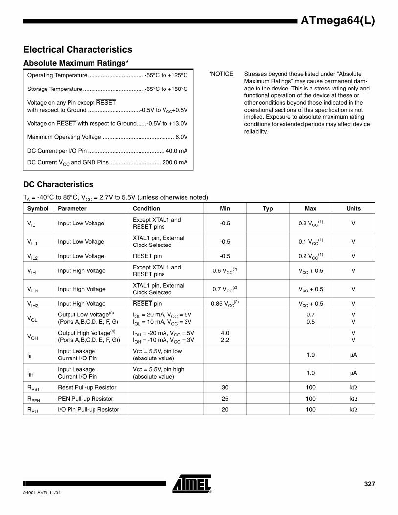
ATmega64(L)
Electrical CharacteristicsAbsolute Maximum Ratings*
Operating Temperature.................................. -55°C to +125°C *NOTICE: Stresses beyond those listed under “Absolute Maximum Ratings” may cause permanent dam-age to the device. This is a stress rating only and functional operation of the device at these or other conditions beyond those indicated in the operational sections of this specification is not implied. Exposure to absolute maximum rating conditions for extended periods may affect device reliability.
Storage Temperature ..................................... -65°C to +150°C
Voltage on any Pin except RESETwith respect to Ground ................................-0.5V to VCC+0.5V
Voltage on RESET with respect to Ground......-0.5V to +13.0V
Maximum Operating Voltage ............................................ 6.0V
DC Current per I/O Pin ............................................... 40.0 mA
DC Current VCC and GND Pins................................ 200.0 mA
DC Characteristics
TA = -40°C to 85°C, VCC = 2.7V to 5.5V (unless otherwise noted)
Symbol Parameter Condition Min Typ Max Units
VIL Input Low VoltageExcept XTAL1 and RESET pins
-0.5 0.2 VCC(1) V
VIL1 Input Low VoltageXTAL1 pin, External Clock Selected
-0.5 0.1 VCC(1) V
VIL2 Input Low Voltage RESET pin -0.5 0.2 VCC(1) V
VIH Input High VoltageExcept XTAL1 and RESET pins
0.6 VCC(2) VCC + 0.5 V
VIH1 Input High VoltageXTAL1 pin, External Clock Selected
0.7 VCC(2) VCC + 0.5 V
VIH2 Input High Voltage RESET pin 0.85 VCC(2) VCC + 0.5 V
VOLOutput Low Voltage(3)
(Ports A,B,C,D, E, F, G)IOL = 20 mA, VCC = 5VIOL = 10 mA, VCC = 3V
0.70.5
VV
VOHOutput High Voltage(4)
(Ports A,B,C,D, E, F, G))IOH = -20 mA, VCC = 5VIOH = -10 mA, VCC = 3V
4.02.2
VV
IILInput LeakageCurrent I/O Pin
Vcc = 5.5V, pin low(absolute value)
1.0 µA
IIHInput LeakageCurrent I/O Pin
Vcc = 5.5V, pin high(absolute value)
1.0 µA
RRST Reset Pull-up Resistor 30 100 kΩ
RPEN PEN Pull-up Resistor 25 100 kΩ
RPU I/O Pin Pull-up Resistor 20 100 kΩ
3272490I–AVR–11/04
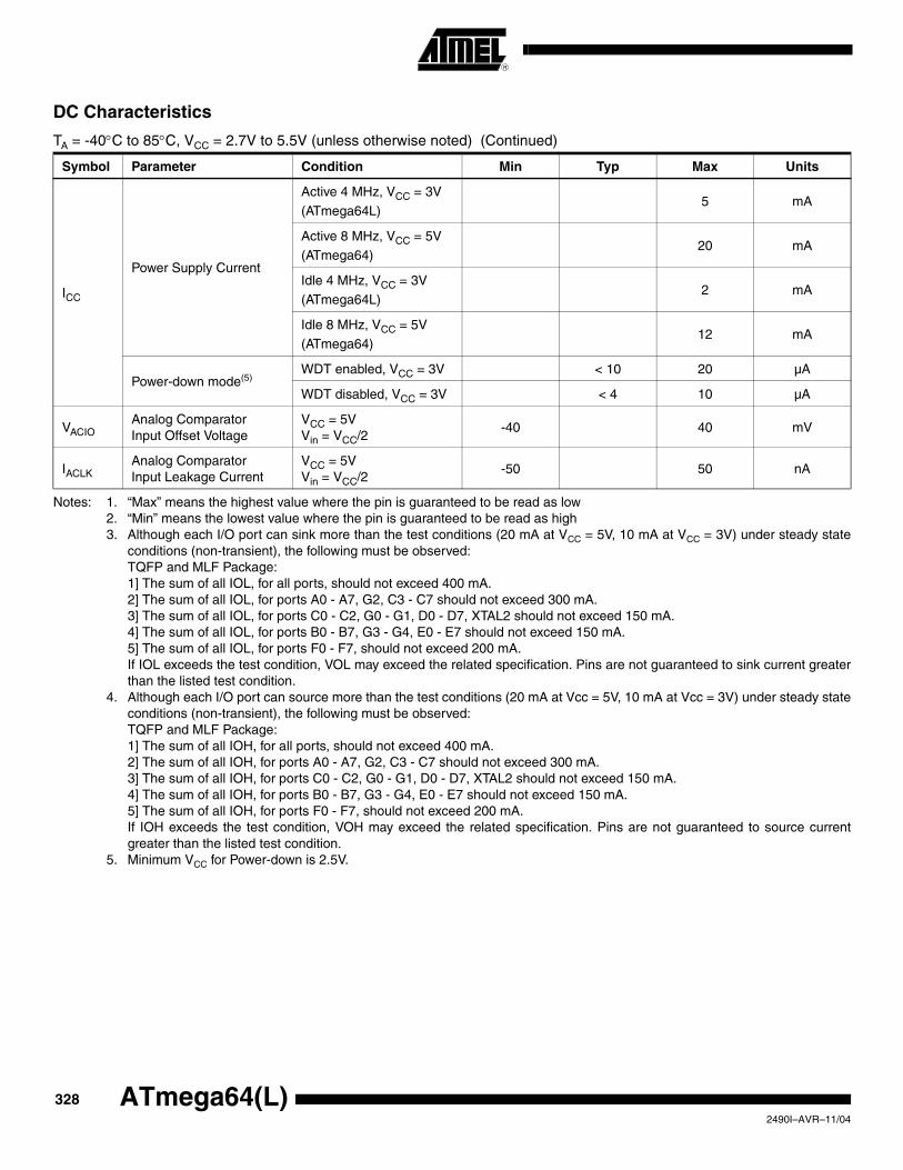
Notes: 1. “Max” means the highest value where the pin is guaranteed to be read as low2. “Min” means the lowest value where the pin is guaranteed to be read as high3. Although each I/O port can sink more than the test conditions (20 mA at VCC = 5V, 10 mA at VCC = 3V) under steady state
conditions (non-transient), the following must be observed:TQFP and MLF Package:1] The sum of all IOL, for all ports, should not exceed 400 mA.2] The sum of all IOL, for ports A0 - A7, G2, C3 - C7 should not exceed 300 mA.3] The sum of all IOL, for ports C0 - C2, G0 - G1, D0 - D7, XTAL2 should not exceed 150 mA.4] The sum of all IOL, for ports B0 - B7, G3 - G4, E0 - E7 should not exceed 150 mA.5] The sum of all IOL, for ports F0 - F7, should not exceed 200 mA.If IOL exceeds the test condition, VOL may exceed the related specification. Pins are not guaranteed to sink current greaterthan the listed test condition.
4. Although each I/O port can source more than the test conditions (20 mA at Vcc = 5V, 10 mA at Vcc = 3V) under steady stateconditions (non-transient), the following must be observed:TQFP and MLF Package:1] The sum of all IOH, for all ports, should not exceed 400 mA.2] The sum of all IOH, for ports A0 - A7, G2, C3 - C7 should not exceed 300 mA.3] The sum of all IOH, for ports C0 - C2, G0 - G1, D0 - D7, XTAL2 should not exceed 150 mA.4] The sum of all IOH, for ports B0 - B7, G3 - G4, E0 - E7 should not exceed 150 mA.5] The sum of all IOH, for ports F0 - F7, should not exceed 200 mA.If IOH exceeds the test condition, VOH may exceed the related specification. Pins are not guaranteed to source currentgreater than the listed test condition.
5. Minimum VCC for Power-down is 2.5V.
ICC
Power Supply Current
Active 4 MHz, VCC = 3V
(ATmega64L)5 mA
Active 8 MHz, VCC = 5V(ATmega64)
20 mA
Idle 4 MHz, VCC = 3V(ATmega64L)
2 mA
Idle 8 MHz, VCC = 5V(ATmega64)
12 mA
Power-down mode(5)WDT enabled, VCC = 3V < 10 20 µA
WDT disabled, VCC = 3V < 4 10 µA
VACIOAnalog Comparator Input Offset Voltage
VCC = 5VVin = VCC/2
-40 40 mV
IACLKAnalog Comparator Input Leakage Current
VCC = 5VVin = VCC/2
-50 50 nA
DC Characteristics
TA = -40°C to 85°C, VCC = 2.7V to 5.5V (unless otherwise noted) (Continued)
Symbol Parameter Condition Min Typ Max Units
328 ATmega64(L)2490I–AVR–11/04
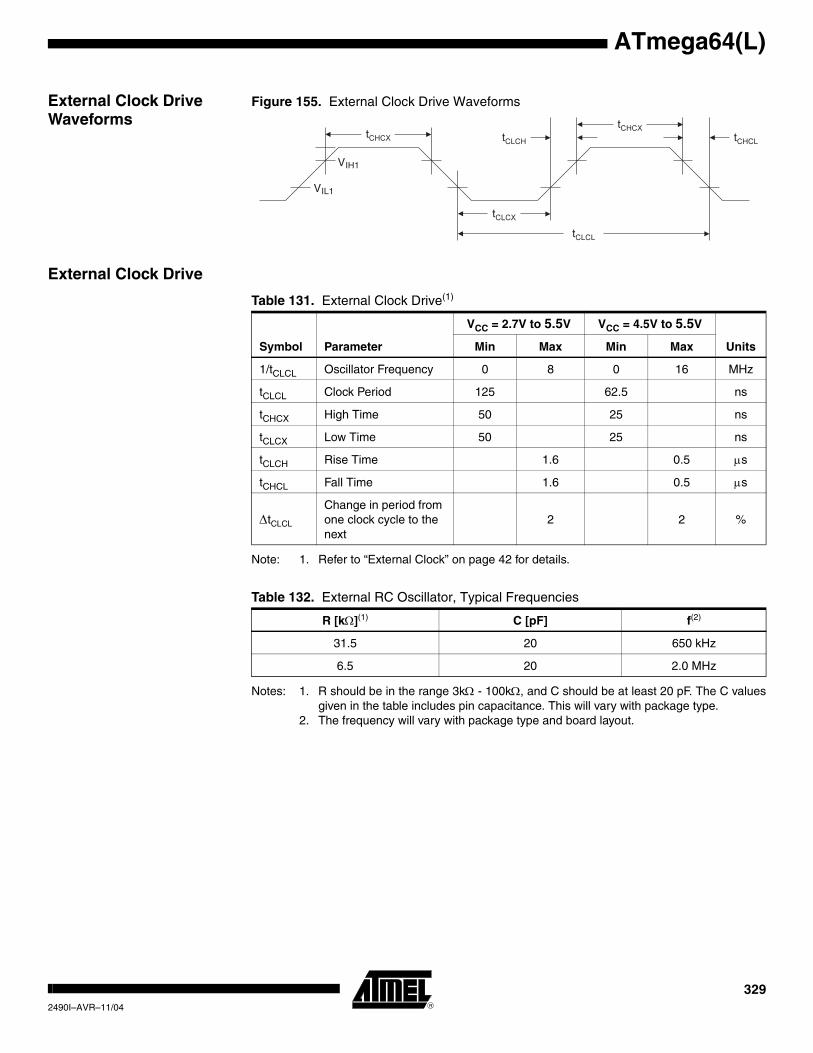
ATmega64(L)
External Clock Drive Waveforms
Figure 155. External Clock Drive Waveforms
External Clock Drive
Note: 1. Refer to “External Clock” on page 42 for details.
Notes: 1. R should be in the range 3kΩ - 100kΩ, and C should be at least 20 pF. The C valuesgiven in the table includes pin capacitance. This will vary with package type.
2. The frequency will vary with package type and board layout.
VIL1
VIH1
Table 131. External Clock Drive(1)
Symbol Parameter
VCC = 2.7V to 5.5V VCC = 4.5V to 5.5V
UnitsMin Max Min Max
1/tCLCL Oscillator Frequency 0 8 0 16 MHz
tCLCL Clock Period 125 62.5 ns
tCHCX High Time 50 25 ns
tCLCX Low Time 50 25 ns
tCLCH Rise Time 1.6 0.5 µs
tCHCL Fall Time 1.6 0.5 µs
∆tCLCL
Change in period from one clock cycle to the next
2 2 %
Table 132. External RC Oscillator, Typical Frequencies
R [kΩ](1) C [pF] f(2)
31.5 20 650 kHz
6.5 20 2.0 MHz
3292490I–AVR–11/04
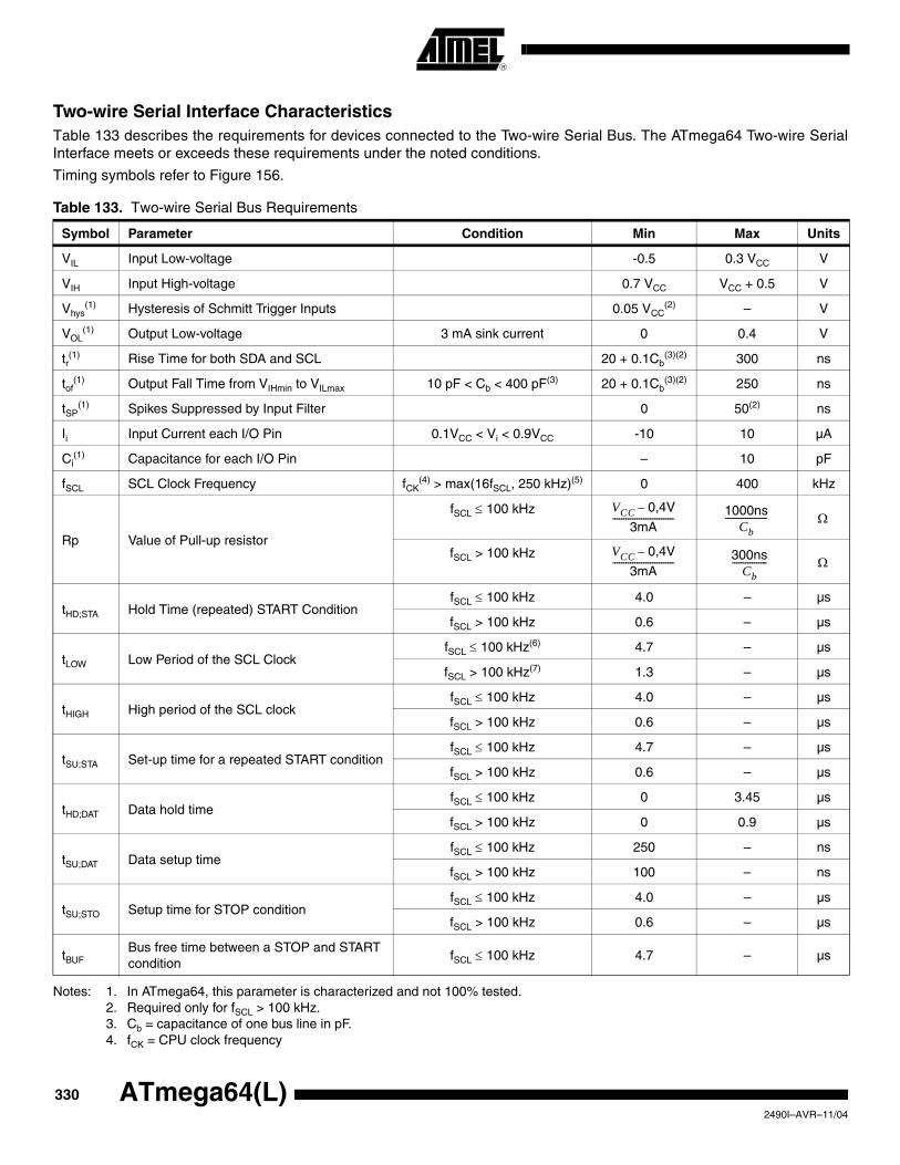
Two-wire Serial Interface CharacteristicsTable 133 describes the requirements for devices connected to the Two-wire Serial Bus. The ATmega64 Two-wire SerialInterface meets or exceeds these requirements under the noted conditions.
Timing symbols refer to Figure 156.
Notes: 1. In ATmega64, this parameter is characterized and not 100% tested.2. Required only for fSCL > 100 kHz.3. Cb = capacitance of one bus line in pF.4. fCK = CPU clock frequency
Table 133. Two-wire Serial Bus Requirements
Symbol Parameter Condition Min Max Units
VIL Input Low-voltage -0.5 0.3 VCC V
VIH Input High-voltage 0.7 VCC VCC + 0.5 V
Vhys(1) Hysteresis of Schmitt Trigger Inputs 0.05 VCC
(2) – V
VOL(1) Output Low-voltage 3 mA sink current 0 0.4 V
tr(1) Rise Time for both SDA and SCL 20 + 0.1Cb
(3)(2) 300 ns
tof(1) Output Fall Time from VIHmin to VILmax 10 pF < Cb < 400 pF(3) 20 + 0.1Cb
(3)(2) 250 ns
tSP(1) Spikes Suppressed by Input Filter 0 50(2) ns
Ii Input Current each I/O Pin 0.1VCC < Vi < 0.9VCC -10 10 µA
Ci(1) Capacitance for each I/O Pin – 10 pF
fSCL SCL Clock Frequency fCK(4) > max(16fSCL, 250 kHz)(5) 0 400 kHz
Rp Value of Pull-up resistor
fSCL ≤ 100 kHz
fSCL > 100 kHz
tHD;STA Hold Time (repeated) START ConditionfSCL ≤ 100 kHz 4.0 – µs
fSCL > 100 kHz 0.6 – µs
tLOW Low Period of the SCL ClockfSCL ≤ 100 kHz(6) 4.7 – µs
fSCL > 100 kHz(7) 1.3 – µs
tHIGH High period of the SCL clockfSCL ≤ 100 kHz 4.0 – µs
fSCL > 100 kHz 0.6 – µs
tSU;STA Set-up time for a repeated START conditionfSCL ≤ 100 kHz 4.7 – µs
fSCL > 100 kHz 0.6 – µs
tHD;DAT Data hold timefSCL ≤ 100 kHz 0 3.45 µs
fSCL > 100 kHz 0 0.9 µs
tSU;DAT Data setup timefSCL ≤ 100 kHz 250 – ns
fSCL > 100 kHz 100 – ns
tSU;STO Setup time for STOP conditionfSCL ≤ 100 kHz 4.0 – µs
fSCL > 100 kHz 0.6 – µs
tBUFBus free time between a STOP and START condition
fSCL ≤ 100 kHz 4.7 – µs
VCC 0,4V–
3mA---------------------------- 1000ns
Cb------------------- Ω
VCC 0,4V–
3mA---------------------------- 300ns
Cb---------------- Ω
330 ATmega64(L)2490I–AVR–11/04
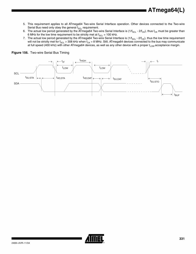
ATmega64(L)
5. This requirement applies to all ATmega64 Two-wire Serial Interface operation. Other devices connected to the Two-wireSerial Bus need only obey the general fSCL requirement.
6. The actual low period generated by the ATmega64 Two-wire Serial Interface is (1/fSCL - 2/fCK), thus fCK must be greater than6 MHz for the low time requirement to be strictly met at fSCL = 100 kHz.
7. The actual low period generated by the ATmega64 Two-wire Serial Interface is (1/fSCL - 2/fCK), thus the low time requirementwill not be strictly met for fSCL > 308 kHz when fCK = 8 MHz. Still, ATmega64 devices connected to the bus may communicateat full speed (400 kHz) with other ATmega64 devices, as well as any other device with a proper tLOW acceptance margin.
Figure 156. Two-wire Serial Bus Timing
tSU;STA
tLOW
tHIGH
tLOW
tof
tHD;STA tHD;DAT tSU;DATtSU;STO
tBUF
SCL
SDA
tr
3312490I–AVR–11/04
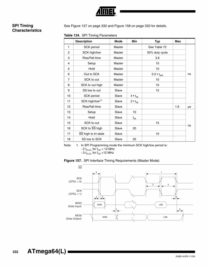
SPI Timing Characteristics
See Figure 157 on page 332 and Figure 158 on page 333 for details.
Note: 1. In SPI Programming mode the minimum SCK high/low period is:- 2 tCLCL for fCK < 12 MHz- 3 tCLCL for fCK >12 MHz
Figure 157. SPI Interface Timing Requirements (Master Mode)
Table 134. SPI Timing Parameters
Description Mode Min Typ Max
1 SCK period Master See Table 72
ns
2 SCK high/low Master 50% duty cycle
3 Rise/Fall time Master 3.6
4 Setup Master 10
5 Hold Master 10
6 Out to SCK Master 0.5 • tsck
7 SCK to out Master 10
8 SCK to out high Master 10
9 SS low to out Slave 15
10 SCK period Slave 4 • tck
11 SCK high/low(1) Slave 2 • tck
12 Rise/Fall time Slave 1.6 µs
13 Setup Slave 10
ns
14 Hold Slave tck
15 SCK to out Slave 15
16 SCK to SS high Slave 20
17 SS high to tri-state Slave 10
18 SS low to SCK Slave 20
MOSI(Data Output)
SCK(CPOL = 1)
MISO(Data Input)
SCK(CPOL = 0)
SS
MSB LSB
LSBMSB
...
...
6 1
2 2
34 5
87
332 ATmega64(L)2490I–AVR–11/04
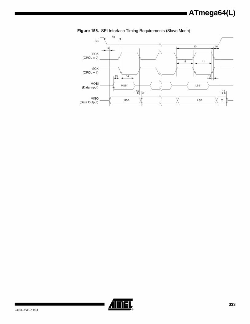
ATmega64(L)
Figure 158. SPI Interface Timing Requirements (Slave Mode)
MISO(Data Output)
SCK(CPOL = 1)
MOSI(Data Input)
SCK(CPOL = 0)
SS
MSB LSB
LSBMSB
...
...
10
11 11
1213 14
1715
9
X
16
18
3332490I–AVR–11/04
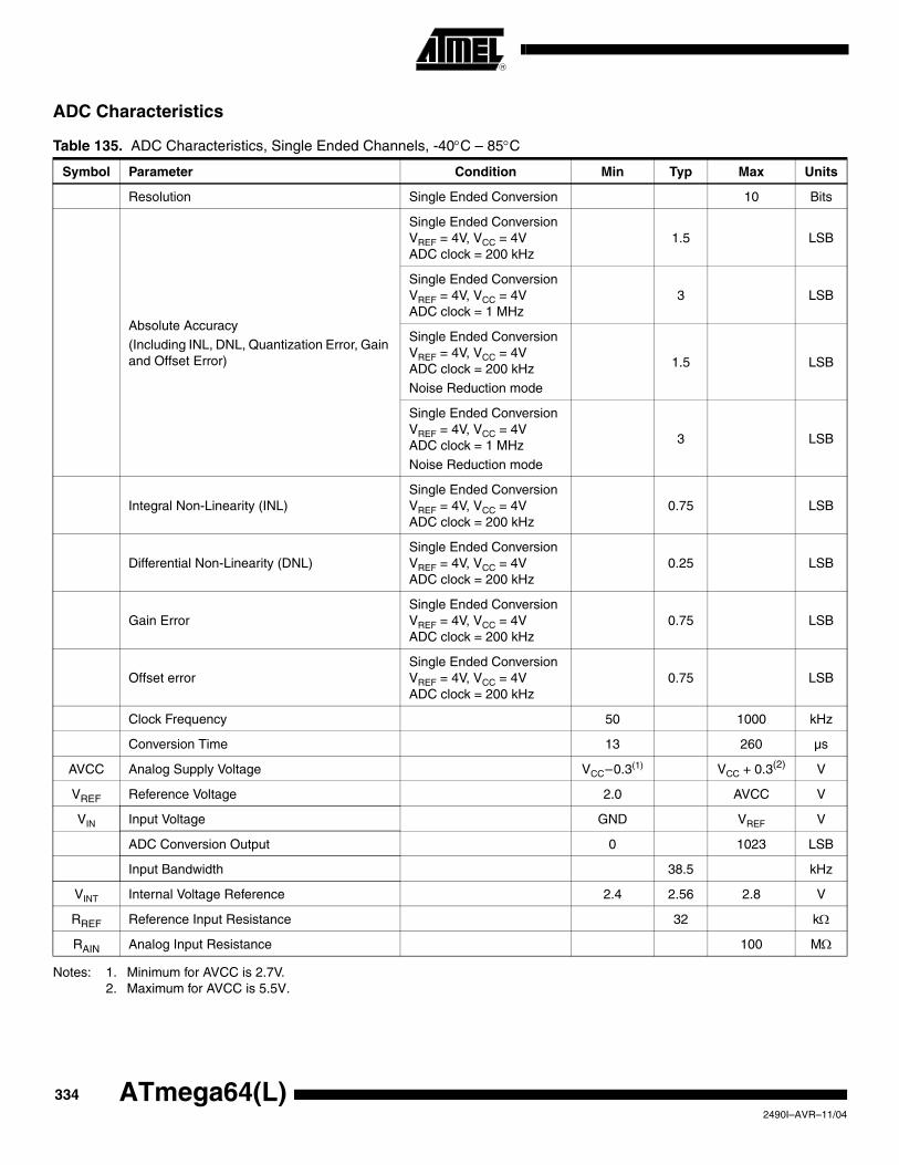
ADC Characteristics
Notes: 1. Minimum for AVCC is 2.7V. 2. Maximum for AVCC is 5.5V.
Table 135. ADC Characteristics, Single Ended Channels, -40°C – 85°C
Symbol Parameter Condition Min Typ Max Units
Resolution Single Ended Conversion 10 Bits
Absolute Accuracy (Including INL, DNL, Quantization Error, Gain and Offset Error)
Single Ended ConversionVREF = 4V, VCC = 4VADC clock = 200 kHz
1.5 LSB
Single Ended ConversionVREF = 4V, VCC = 4VADC clock = 1 MHz
3 LSB
Single Ended ConversionVREF = 4V, VCC = 4VADC clock = 200 kHz
Noise Reduction mode
1.5 LSB
Single Ended ConversionVREF = 4V, VCC = 4VADC clock = 1 MHz
Noise Reduction mode
3 LSB
Integral Non-Linearity (INL)Single Ended ConversionVREF = 4V, VCC = 4VADC clock = 200 kHz
0.75 LSB
Differential Non-Linearity (DNL)Single Ended ConversionVREF = 4V, VCC = 4VADC clock = 200 kHz
0.25 LSB
Gain ErrorSingle Ended ConversionVREF = 4V, VCC = 4VADC clock = 200 kHz
0.75 LSB
Offset errorSingle Ended ConversionVREF = 4V, VCC = 4VADC clock = 200 kHz
0.75 LSB
Clock Frequency 50 1000 kHz
Conversion Time 13 260 µs
AVCC Analog Supply Voltage VCC–0.3(1) VCC + 0.3(2) V
VREF Reference Voltage 2.0 AVCC V
VIN Input Voltage GND VREF V
ADC Conversion Output 0 1023 LSB
Input Bandwidth 38.5 kHz
VINT Internal Voltage Reference 2.4 2.56 2.8 V
RREF Reference Input Resistance 32 kΩ
RAIN Analog Input Resistance 100 MΩ
334 ATmega64(L)2490I–AVR–11/04
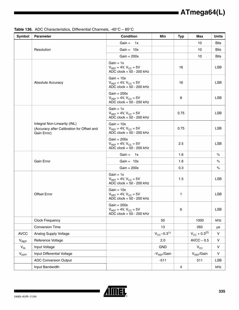
ATmega64(L)
Table 136. ADC Characteristics, Differential Channels, -40°C – 85°C
Symbol Parameter Condition Min Typ Max Units
Resolution
Gain = 1x 10 Bits
Gain = 10x 10 Bits
Gain = 200x 10 Bits
Absolute Accuracy
Gain = 1xVREF = 4V, VCC = 5VADC clock = 50 - 200 kHz
16 LSB
Gain = 10xVREF = 4V, VCC = 5VADC clock = 50 - 200 kHz
16 LSB
Gain = 200xVREF = 4V, VCC = 5VADC clock = 50 - 200 kHz
8 LSB
Integral Non-Linearity (INL)(Accuracy after Calibration for Offset and Gain Error)
Gain = 1xVREF = 4V, VCC = 5VADC clock = 50 - 200 kHz
0.75 LSB
Gain = 10xVREF = 4V, VCC = 5VADC clock = 50 - 200 kHz
0.75 LSB
Gain = 200xVREF = 4V, VCC = 5VADC clock = 50 - 200 kHz
2.5 LSB
Gain Error
Gain = 1x 1.6 %
Gain = 10x 1.6 %
Gain = 200x 0.3 %
Offset Error
Gain = 1xVREF = 4V, VCC = 5VADC clock = 50 - 200 kHz
1.5 LSB
Gain = 10xVREF = 4V, VCC = 5VADC clock = 50 - 200 kHz
1 LSB
Gain = 200xVREF = 4V, VCC = 5VADC clock = 50 - 200 kHz
6 LSB
Clock Frequency 50 1000 kHz
Conversion Time 13 260 µs
AVCC Analog Supply Voltage VCC–0.3(1) VCC + 0.3(2) V
VREF Reference Voltage 2.0 AVCC – 0.5 V
VIN Input Voltage GND VCC V
VDIFF Input Differential Voltage -VREF/Gain VREF/Gain V
ADC Conversion Output -511 511 LSB
Input Bandwidth 4 kHz
3352490I–AVR–11/04
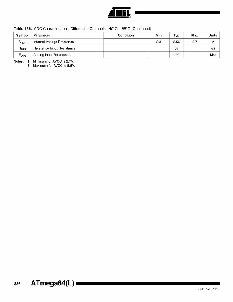
Notes: 1. Minimum for AVCC is 2.7V.2. Maximum for AVCC is 5.5V.
VINT Internal Voltage Reference 2.3 2.56 2.7 V
RREF Reference Input Resistance 32 kΩ
RAIN Analog Input Resistance 100 MΩ
Table 136. ADC Characteristics, Differential Channels, -40°C – 85°C (Continued)
Symbol Parameter Condition Min Typ Max Units
336 ATmega64(L)2490I–AVR–11/04
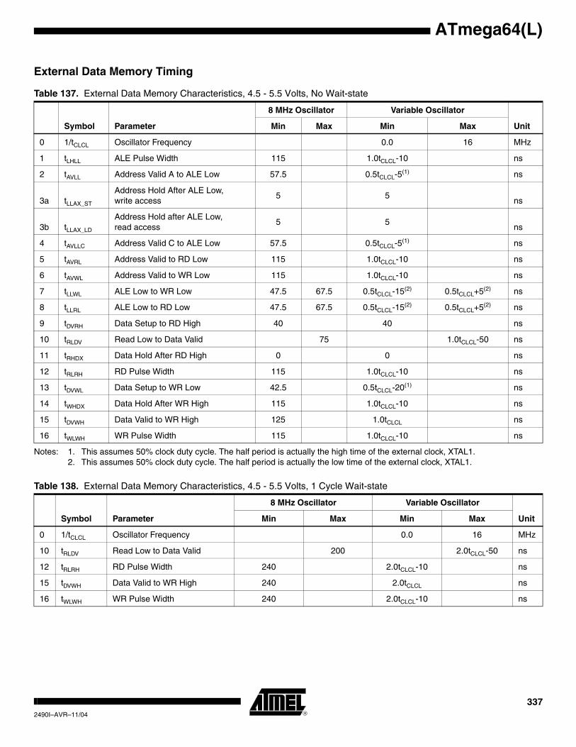
ATmega64(L)
External Data Memory Timing
Notes: 1. This assumes 50% clock duty cycle. The half period is actually the high time of the external clock, XTAL1.2. This assumes 50% clock duty cycle. The half period is actually the low time of the external clock, XTAL1.
Table 137. External Data Memory Characteristics, 4.5 - 5.5 Volts, No Wait-state
Symbol Parameter
8 MHz Oscillator Variable Oscillator
UnitMin Max Min Max
0 1/tCLCL Oscillator Frequency 0.0 16 MHz
1 tLHLL ALE Pulse Width 115 1.0tCLCL-10 ns
2 tAVLL Address Valid A to ALE Low 57.5 0.5tCLCL-5(1) ns
3a tLLAX_ST
Address Hold After ALE Low, write access
5 5ns
3b tLLAX_LD
Address Hold after ALE Low, read access
5 5ns
4 tAVLLC Address Valid C to ALE Low 57.5 0.5tCLCL-5(1) ns
5 tAVRL Address Valid to RD Low 115 1.0tCLCL-10 ns
6 tAVWL Address Valid to WR Low 115 1.0tCLCL-10 ns
7 tLLWL ALE Low to WR Low 47.5 67.5 0.5tCLCL-15(2) 0.5tCLCL+5(2) ns
8 tLLRL ALE Low to RD Low 47.5 67.5 0.5tCLCL-15(2) 0.5tCLCL+5(2) ns
9 tDVRH Data Setup to RD High 40 40 ns
10 tRLDV Read Low to Data Valid 75 1.0tCLCL-50 ns
11 tRHDX Data Hold After RD High 0 0 ns
12 tRLRH RD Pulse Width 115 1.0tCLCL-10 ns
13 tDVWL Data Setup to WR Low 42.5 0.5tCLCL-20(1) ns
14 tWHDX Data Hold After WR High 115 1.0tCLCL-10 ns
15 tDVWH Data Valid to WR High 125 1.0tCLCL ns
16 tWLWH WR Pulse Width 115 1.0tCLCL-10 ns
Table 138. External Data Memory Characteristics, 4.5 - 5.5 Volts, 1 Cycle Wait-state
Symbol Parameter
8 MHz Oscillator Variable Oscillator
UnitMin Max Min Max
0 1/tCLCL Oscillator Frequency 0.0 16 MHz
10 tRLDV Read Low to Data Valid 200 2.0tCLCL-50 ns
12 tRLRH RD Pulse Width 240 2.0tCLCL-10 ns
15 tDVWH Data Valid to WR High 240 2.0tCLCL ns
16 tWLWH WR Pulse Width 240 2.0tCLCL-10 ns
3372490I–AVR–11/04
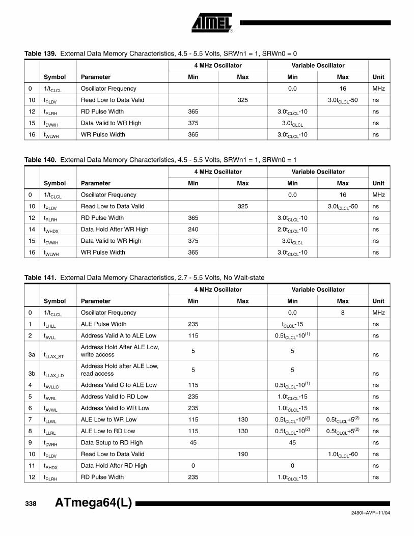
Table 139. External Data Memory Characteristics, 4.5 - 5.5 Volts, SRWn1 = 1, SRWn0 = 0
Symbol Parameter
4 MHz Oscillator Variable Oscillator
UnitMin Max Min Max
0 1/tCLCL Oscillator Frequency 0.0 16 MHz
10 tRLDV Read Low to Data Valid 325 3.0tCLCL-50 ns
12 tRLRH RD Pulse Width 365 3.0tCLCL-10 ns
15 tDVWH Data Valid to WR High 375 3.0tCLCL ns
16 tWLWH WR Pulse Width 365 3.0tCLCL-10 ns
Table 140. External Data Memory Characteristics, 4.5 - 5.5 Volts, SRWn1 = 1, SRWn0 = 1
Symbol Parameter
4 MHz Oscillator Variable Oscillator
UnitMin Max Min Max
0 1/tCLCL Oscillator Frequency 0.0 16 MHz
10 tRLDV Read Low to Data Valid 325 3.0tCLCL-50 ns
12 tRLRH RD Pulse Width 365 3.0tCLCL-10 ns
14 tWHDX Data Hold After WR High 240 2.0tCLCL-10 ns
15 tDVWH Data Valid to WR High 375 3.0tCLCL ns
16 tWLWH WR Pulse Width 365 3.0tCLCL-10 ns
Table 141. External Data Memory Characteristics, 2.7 - 5.5 Volts, No Wait-state
Symbol Parameter
4 MHz Oscillator Variable Oscillator
UnitMin Max Min Max
0 1/tCLCL Oscillator Frequency 0.0 8 MHz
1 tLHLL ALE Pulse Width 235 tCLCL-15 ns
2 tAVLL Address Valid A to ALE Low 115 0.5tCLCL-10(1) ns
3a tLLAX_ST
Address Hold After ALE Low, write access
5 5ns
3b tLLAX_LD
Address Hold after ALE Low, read access
5 5ns
4 tAVLLC Address Valid C to ALE Low 115 0.5tCLCL-10(1) ns
5 tAVRL Address Valid to RD Low 235 1.0tCLCL-15 ns
6 tAVWL Address Valid to WR Low 235 1.0tCLCL-15 ns
7 tLLWL ALE Low to WR Low 115 130 0.5tCLCL-10(2) 0.5tCLCL+5(2) ns
8 tLLRL ALE Low to RD Low 115 130 0.5tCLCL-10(2) 0.5tCLCL+5(2) ns
9 tDVRH Data Setup to RD High 45 45 ns
10 tRLDV Read Low to Data Valid 190 1.0tCLCL-60 ns
11 tRHDX Data Hold After RD High 0 0 ns
12 tRLRH RD Pulse Width 235 1.0tCLCL-15 ns
338 ATmega64(L)2490I–AVR–11/04
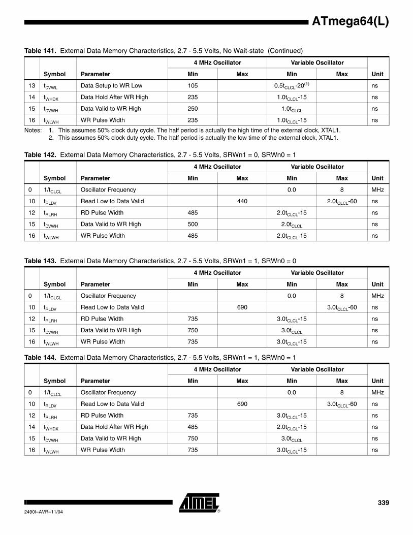
ATmega64(L)
Notes: 1. This assumes 50% clock duty cycle. The half period is actually the high time of the external clock, XTAL1.2. This assumes 50% clock duty cycle. The half period is actually the low time of the external clock, XTAL1.
13 tDVWL Data Setup to WR Low 105 0.5tCLCL-20(1) ns
14 tWHDX Data Hold After WR High 235 1.0tCLCL-15 ns
15 tDVWH Data Valid to WR High 250 1.0tCLCL ns
16 tWLWH WR Pulse Width 235 1.0tCLCL-15 ns
Table 141. External Data Memory Characteristics, 2.7 - 5.5 Volts, No Wait-state (Continued)
Symbol Parameter
4 MHz Oscillator Variable Oscillator
UnitMin Max Min Max
Table 142. External Data Memory Characteristics, 2.7 - 5.5 Volts, SRWn1 = 0, SRWn0 = 1
Symbol Parameter
4 MHz Oscillator Variable Oscillator
UnitMin Max Min Max
0 1/tCLCL Oscillator Frequency 0.0 8 MHz
10 tRLDV Read Low to Data Valid 440 2.0tCLCL-60 ns
12 tRLRH RD Pulse Width 485 2.0tCLCL-15 ns
15 tDVWH Data Valid to WR High 500 2.0tCLCL ns
16 tWLWH WR Pulse Width 485 2.0tCLCL-15 ns
Table 143. External Data Memory Characteristics, 2.7 - 5.5 Volts, SRWn1 = 1, SRWn0 = 0
Symbol Parameter
4 MHz Oscillator Variable Oscillator
UnitMin Max Min Max
0 1/tCLCL Oscillator Frequency 0.0 8 MHz
10 tRLDV Read Low to Data Valid 690 3.0tCLCL-60 ns
12 tRLRH RD Pulse Width 735 3.0tCLCL-15 ns
15 tDVWH Data Valid to WR High 750 3.0tCLCL ns
16 tWLWH WR Pulse Width 735 3.0tCLCL-15 ns
Table 144. External Data Memory Characteristics, 2.7 - 5.5 Volts, SRWn1 = 1, SRWn0 = 1
Symbol Parameter
4 MHz Oscillator Variable Oscillator
UnitMin Max Min Max
0 1/tCLCL Oscillator Frequency 0.0 8 MHz
10 tRLDV Read Low to Data Valid 690 3.0tCLCL-60 ns
12 tRLRH RD Pulse Width 735 3.0tCLCL-15 ns
14 tWHDX Data Hold After WR High 485 2.0tCLCL-15 ns
15 tDVWH Data Valid to WR High 750 3.0tCLCL ns
16 tWLWH WR Pulse Width 735 3.0tCLCL-15 ns
3392490I–AVR–11/04
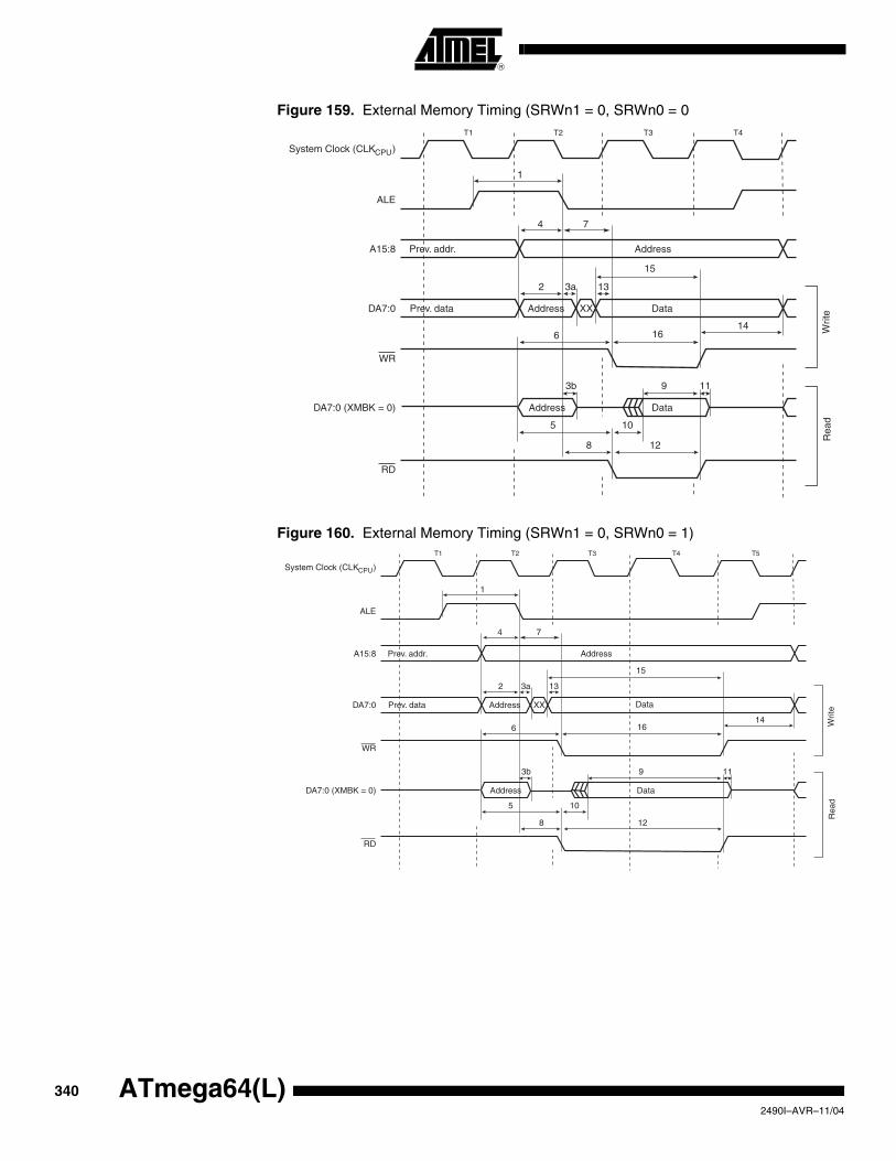
Figure 159. External Memory Timing (SRWn1 = 0, SRWn0 = 0
Figure 160. External Memory Timing (SRWn1 = 0, SRWn0 = 1)
ALE
T1 T2 T3
Writ
eR
ead
WR
T4
A15:8 AddressPrev. addr.
DA7:0 Address DataPrev. data XX
RD
DA7:0 (XMBK = 0) DataAddress
System Clock (CLKCPU)
1
4
2
7
6
3a
3b
5
8 12
16
13
10
11
14
15
9
ALE
T1 T2 T3
Writ
eR
ead
WR
T5
A15:8 AddressPrev. addr.
DA7:0 Address DataPrev. data XX
RD
DA7:0 (XMBK = 0) DataAddress
System Clock (CLKCPU)
1
4
2
7
6
3a
3b
5
8 12
16
13
10
11
14
15
9
T4
340 ATmega64(L)2490I–AVR–11/04
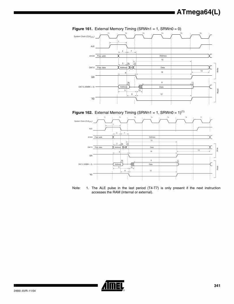
ATmega64(L)
Figure 161. External Memory Timing (SRWn1 = 1, SRWn0 = 0)
Figure 162. External Memory Timing (SRWn1 = 1, SRWn0 = 1)(1)
Note: 1. The ALE pulse in the last period (T4-T7) is only present if the next instructionaccesses the RAM (internal or external).
ALE
T1 T2 T3
Writ
eR
ead
WR
T6
A15:8 AddressPrev. addr.
DA7:0 Address DataPrev. data XX
RD
DA7:0 (XMBK = 0) DataAddress
System Clock (CLKCPU)
1
4
2
7
6
3a
3b
5
8 12
16
13
10
11
14
15
9
T4 T5
ALE
T1 T2 T3
Writ
eR
ead
WR
T7
A15:8 AddressPrev. addr.
DA7:0 Address DataPrev. data XX
RD
DA7:0 (XMBK = 0) DataAddress
System Clock (CLKCPU)
1
4
2
7
6
3a
3b
5
8 12
16
13
10
11
14
15
9
T4 T5 T6
3412490I–AVR–11/04
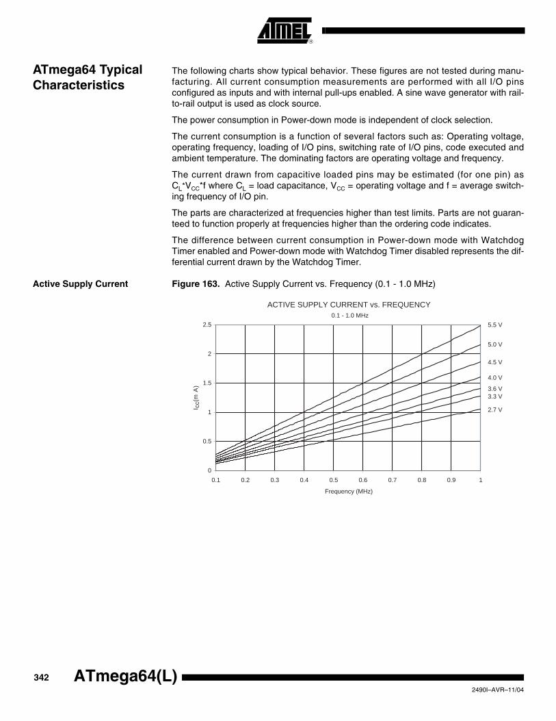
ATmega64 Typical Characteristics
The following charts show typical behavior. These figures are not tested during manu-facturing. All current consumption measurements are performed with all I/O pinsconfigured as inputs and with internal pull-ups enabled. A sine wave generator with rail-to-rail output is used as clock source.
The power consumption in Power-down mode is independent of clock selection.
The current consumption is a function of several factors such as: Operating voltage,operating frequency, loading of I/O pins, switching rate of I/O pins, code executed andambient temperature. The dominating factors are operating voltage and frequency.
The current drawn from capacitive loaded pins may be estimated (for one pin) asCL*VCC*f where CL = load capacitance, VCC = operating voltage and f = average switch-ing frequency of I/O pin.
The parts are characterized at frequencies higher than test limits. Parts are not guaran-teed to function properly at frequencies higher than the ordering code indicates.
The difference between current consumption in Power-down mode with WatchdogTimer enabled and Power-down mode with Watchdog Timer disabled represents the dif-ferential current drawn by the Watchdog Timer.
Active Supply Current Figure 163. Active Supply Current vs. Frequency (0.1 - 1.0 MHz)
ACTIVE SUPPLY CURRENT vs. FREQUENCY0.1 - 1.0 MHz
5.5 V
5.0 V
4.5 V
4.0 V
3.6 V3.3 V
2.7 V
0
0.5
1
1.5
2
2.5
0.1 0.2 0.3 0.4 0.5 0.6 0.7 0.8 0.9 1
Frequency (MHz)
I cc(
mA
)
342 ATmega64(L)2490I–AVR–11/04
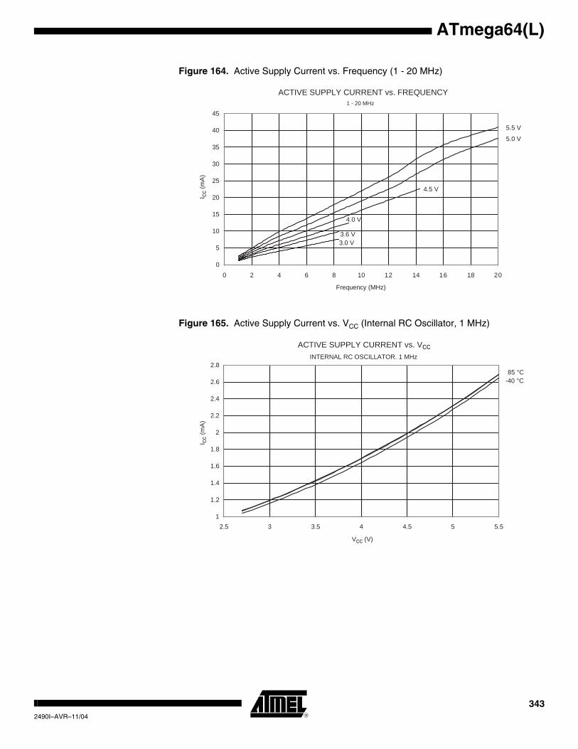
ATmega64(L)
Figure 164. Active Supply Current vs. Frequency (1 - 20 MHz)
Figure 165. Active Supply Current vs. VCC (Internal RC Oscillator, 1 MHz)
ACTIVE SUPPLY CURRENT vs. FREQUENCY1 - 20 MHz
5.5 V
5.0 V
4.5 V
4.0 V
3.6 V3.0 V
0
5
10
15
20
25
30
35
40
45
0 2 4 6 8 10 12 14 16 18 20
Frequency (MHz)
I cc
(mA
)
ACTIVE SUPPLY CURRENT vs. VccINTERNAL RC OSCILLATOR. 1 MHz
85 °C-40 °C
1
1.2
1.4
1.6
1.8
2
2.2
2.4
2.6
2.8
2.5 3 3.5 4 4.5 5 5.5
Vcc (V)
I cc
(mA
)
3432490I–AVR–11/04

Figure 166. Active Supply Current vs. VCC (Internal RC Oscillator, 2 MHz)
Figure 167. Active Supply Current vs. VCC (Internal RC Oscillator, 4 MHz)
ACTIVE SUPPLY CURRENT vs. VccINTERNAL RC OSCILLATOR. 2 MHz
85 °C25 °C-40 °C
2
2.5
3
3.5
4
4.5
5
5.5
2.5 3 3.5 4 4.5 5 5.5
Vcc (V)
I cc
(mA
)
ACTIVE SUPPLY CURRENT vs. VccINTERNAL RC OSCILLATOR. 4 MHz
85 °C
25 °C-40 °C
3
4
5
6
7
8
9
10
11
2.5 3 3.5 4 4.5 5 5.5
Vcc (V)
I cc
(mA
)
344 ATmega64(L)2490I–AVR–11/04
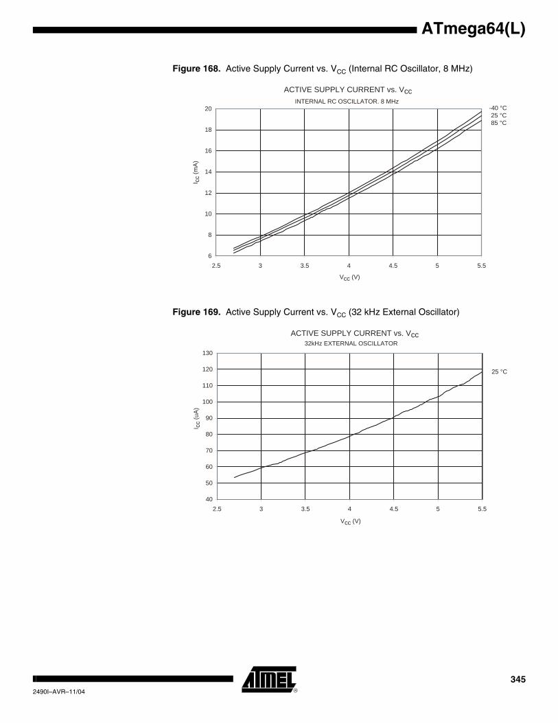
ATmega64(L)
Figure 168. Active Supply Current vs. VCC (Internal RC Oscillator, 8 MHz)
Figure 169. Active Supply Current vs. VCC (32 kHz External Oscillator)
ACTIVE SUPPLY CURRENT vs. VccINTERNAL RC OSCILLATOR. 8 MHz
85 °C25 °C
-40 °C
6
8
10
12
14
16
18
20
2.5 3 3.5 4 4.5 5 5.5
Vcc (V)
I cc
(mA
)
ACTIVE SUPPLY CURRENT vs. Vcc32kHz EXTERNAL OSCILLATOR
25 °C
40
50
60
70
80
90
100
110
120
130
2.5 3 3.5 4 4.5 5 5.5
Vcc (V)
I cc
(uA
)
3452490I–AVR–11/04
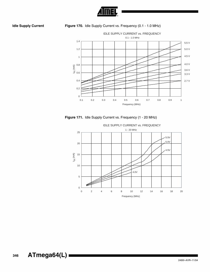
Idle Supply Current Figure 170. Idle Supply Current vs. Frequency (0.1 - 1.0 MHz)
Figure 171. Idle Supply Current vs. Frequency (1 - 20 MHz)
IDLE SUPPLY CURRENT vs. FREQUENCY0.1 - 1.0 MHz
5.5 V
5.0 V
4.5 V
4.0 V
3.6 V
3.3 V
2.7 V
0
0.2
0.4
0.6
0.8
1
1.2
1.4
0.1 0.2 0.3 0.4 0.5 0.6 0.7 0.8 0.9 1
Frequency (MHz)
I cc
(mA
)
IDLE SUPPLY CURRENT vs. FREQUENCY1 - 20 MHz
0
5
10
15
20
25
0 2 4 6 8 10 12 14 16 18 20
Frequency (MHz)
I cc
(mA)
4.0V
4.5V
5.0V
5.5V
346 ATmega64(L)2490I–AVR–11/04
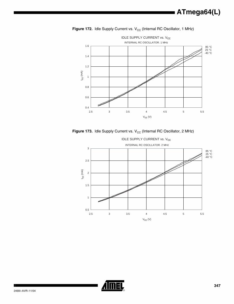
ATmega64(L)
Figure 172. Idle Supply Current vs. VCC (Internal RC Oscillator, 1 MHz)
Figure 173. Idle Supply Current vs. VCC (Internal RC Oscillator, 2 MHz)
IDLE SUPPLY CURRENT vs. VccINTERNAL RC OSCILLATOR. 1 MHz
85 °C25 °C-40 °C
0.4
0.6
0.8
1
1.2
1.4
1.6
2.5 3 3.5 4 4.5 5 5.5
Vcc (V)
I cc
(mA
)
IDLE SUPPLY CURRENT vs. VccINTERNAL RC OSCILLATOR. 2 MHz
85 °C25 °C-40 °C
0.5
1
1.5
2
2.5
3
2.5 3 3.5 4 4.5 5 5.5
Vcc (V)
I cc
(mA
)
3472490I–AVR–11/04
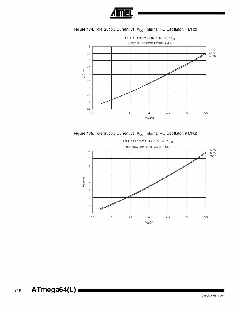
Figure 174. Idle Supply Current vs. VCC (Internal RC Oscillator, 4 MHz)
Figure 175. Idle Supply Current vs. VCC (Internal RC Oscillator, 8 MHz)
IDLE SUPPLY CURRENT vs. VccINTERNAL RC OSCILLATOR. 4 MHz
85 °C25 °C
-40 °C
1.5
2
2.5
3
3.5
4
4.5
5
5.5
6
2.5 3 3.5 4 4.5 5 5.5
Vcc (V)
I cc
(mA
)
IDLE SUPPLY CURRENT vs. VccINTERNAL RC OSCILLATOR. 8 MHz
85 °C25 °C
-40 °C
3
4
5
6
7
8
9
10
11
2.5 3 3.5 4 4.5 5 5.5
Vcc (V)
I cc
(mA
)
348 ATmega64(L)2490I–AVR–11/04

ATmega64(L)
Figure 176. Idle Supply Current vs. VCC (32 kHz External Oscillator)
Power-Down Supply Current Figure 177. Power-Down Supply Current vs. VCC (Watchdog Timer Disabled)
IDLE SUPPLY CURRENT vs. Vcc32kHz EXTERNAL OSCILLATOR
25 °C
30
35
40
45
50
55
60
65
70
75
80
2.5 3 3.5 4 4.5 5 5.5
Vcc (V)
I cc
(uA
)
POWER-DOWN SUPPLY CURRENT vs. VccWATCHDOG TIMER DISABLED
85 °C
25 °C
-40 °C
0
0.5
1
1.5
2
2.5
3
3.5
4
2.5 3 3.5 4 4.5 5 5.5
Vcc (V)
I cc
(uA
)
3492490I–AVR–11/04
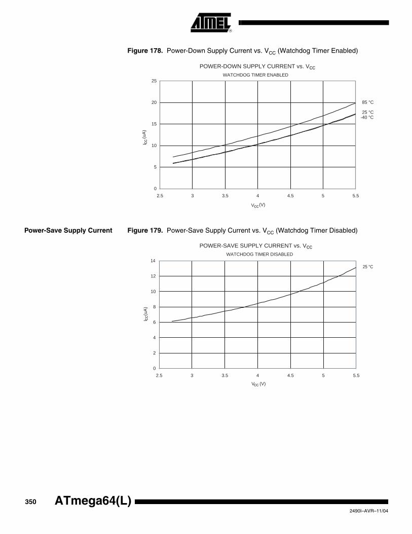
Figure 178. Power-Down Supply Current vs. VCC (Watchdog Timer Enabled)
Power-Save Supply Current Figure 179. Power-Save Supply Current vs. VCC (Watchdog Timer Disabled)
POWER-DOWN SUPPLY CURRENT vs. VccWATCHDOG TIMER ENABLED
85 °C
25 °C-40 °C
0
5
10
15
20
25
2.5 3 3.5 4 4.5 5 5.5
Vcc (V)
I cc
(uA
)
POWER-SAVE SUPPLY CURRENT vs. VccWATCHDOG TIMER DISABLED
25 °C
0
2
4
6
8
10
12
14
2.5 3 3.5 4 4.5 5 5.5
Vcc (V)
I cc (u
A)
350 ATmega64(L)2490I–AVR–11/04
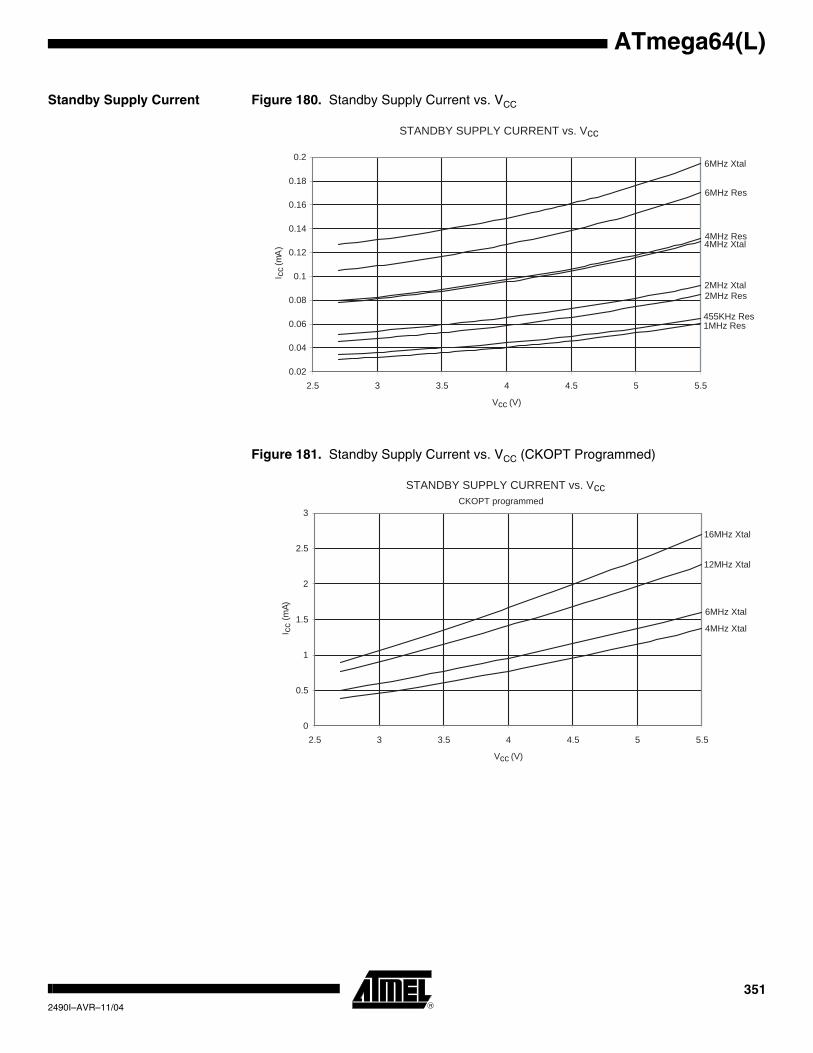
ATmega64(L)
Standby Supply Current Figure 180. Standby Supply Current vs. VCC
Figure 181. Standby Supply Current vs. VCC (CKOPT Programmed)
STANDBY SUPPLY CURRENT vs. Vcc
6MHz Xtal
6MHz Res
4MHz Xtal 4MHz Res
455KHz Res
2MHz Xtal 2MHz Res
1MHz Res
0.02
0.04
0.06
0.08
0.1
0.12
0.14
0.16
0.18
0.2
2.5 3 3.5 4 4.5 5 5.5
Vcc (V)
I cc
(mA
)
STANDBY SUPPLY CURRENT vs. VccCKOPT programmed
6MHz Xtal
4MHz Xtal
16MHz Xtal
12MHz Xtal
0
0.5
1
1.5
2
2.5
3
2.5 3 3.5 4 4.5 5 5.5
Vcc (V)
I cc
(mA)
3512490I–AVR–11/04
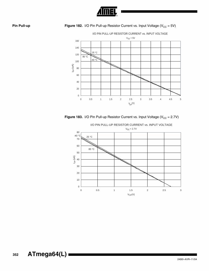
Pin Pull-up Figure 182. I/O Pin Pull-up Resistor Current vs. Input Voltage (VCC = 5V)
Figure 183. I/O Pin Pull-up Resistor Current vs. Input Voltage (VCC = 2.7V)
I/O PIN PULL-UP RESISTOR CURRENT vs. INPUT VOLTAGEVcc = 5V
85 °C
25 °C
-40 °C
0
20
40
60
80
100
120
140
160
0 0.5 1 1.5 2 2.5 3 3.5 4 4.5 5
VOP (V)
I OP
(uA
)
I/O PIN PULL-UP RESISTOR CURRENT vs. INPUT VOLTAGEVcc = 2.7V
85 °C
25 °C-40 °C
0
10
20
30
40
50
60
70
80
0 0.5 1 1.5 2 2.5 3
VOP (V)
I OP
(uA
)
352 ATmega64(L)2490I–AVR–11/04
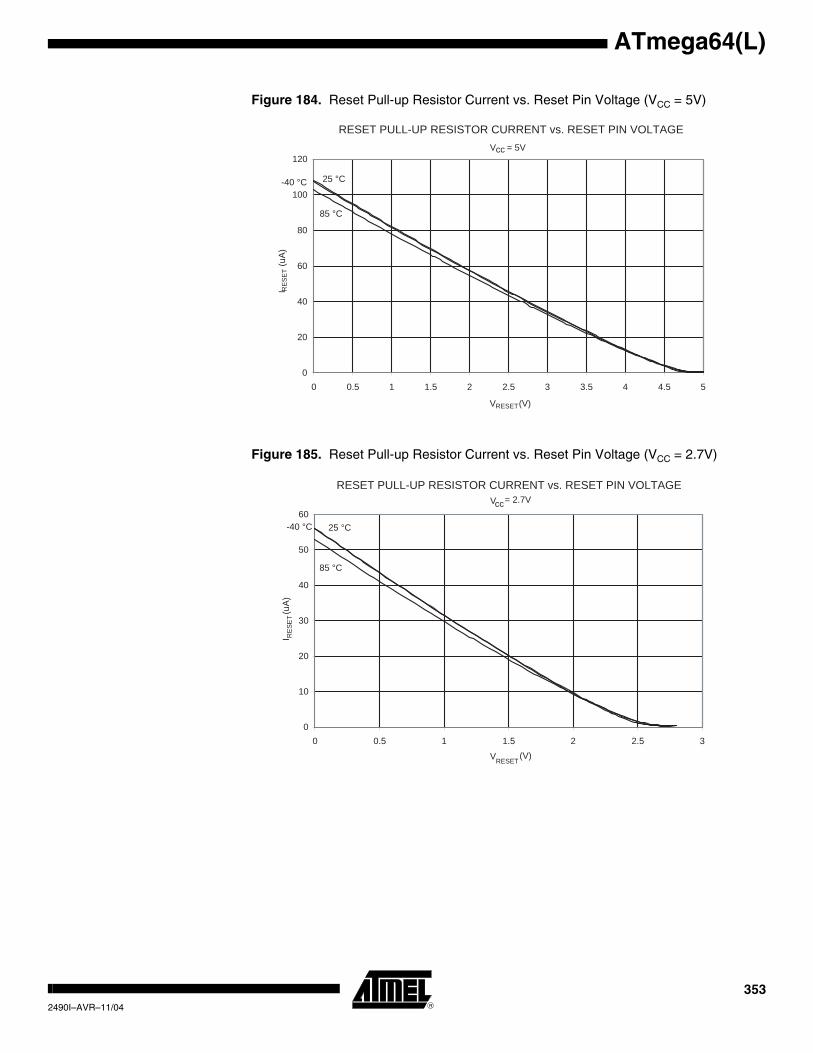
ATmega64(L)
Figure 184. Reset Pull-up Resistor Current vs. Reset Pin Voltage (VCC = 5V)
Figure 185. Reset Pull-up Resistor Current vs. Reset Pin Voltage (VCC = 2.7V)
RESET PULL-UP RESISTOR CURRENT vs. RESET PIN VOLTAGEVcc = 5V
85 °C
25 °C-40 °C
0
20
40
60
80
100
120
0 0.5 1 1.5 2 2.5 3 3.5 4 4.5 5
VRESET (V)
I RES
ET (u
A)
RESET PULL-UP RESISTOR CURRENT vs. RESET PIN VOLTAGEVcc = 2.7V
85 °C
25 °C-40 °C
0
10
20
30
40
50
60
0 0.5 1 1.5 2 2.5 3
VRESET (V)
I RES
ET (u
A)
3532490I–AVR–11/04
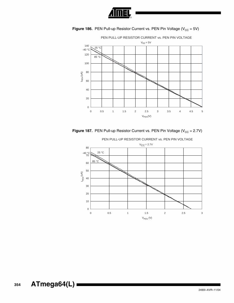
Figure 186. PEN Pull-up Resistor Current vs. PEN Pin Voltage (VCC = 5V)
Figure 187. PEN Pull-up Resistor Current vs. PEN Pin Voltage (VCC = 2.7V)
PEN PULL-UP RESISTOR CURRENT vs. PEN PIN VOLTAGEVcc = 5V
85 °C
25 °C-40 °C
0
20
40
60
80
100
120
140
0 0.5 1 1.5 2 2.5 3 3.5 4 4.5 5
VPEN (V)
I PEN
(uA
)
PEN PULL-UP RESISTOR CURRENT vs. PEN PIN VOLTAGEVCC = 2.7V
85 °C
25 °C-40 °C
0
10
20
30
40
50
60
70
80
0 0.5 1 1.5 2 2.5 3
VPEN (V)
I PEN
(uA
)
354 ATmega64(L)2490I–AVR–11/04
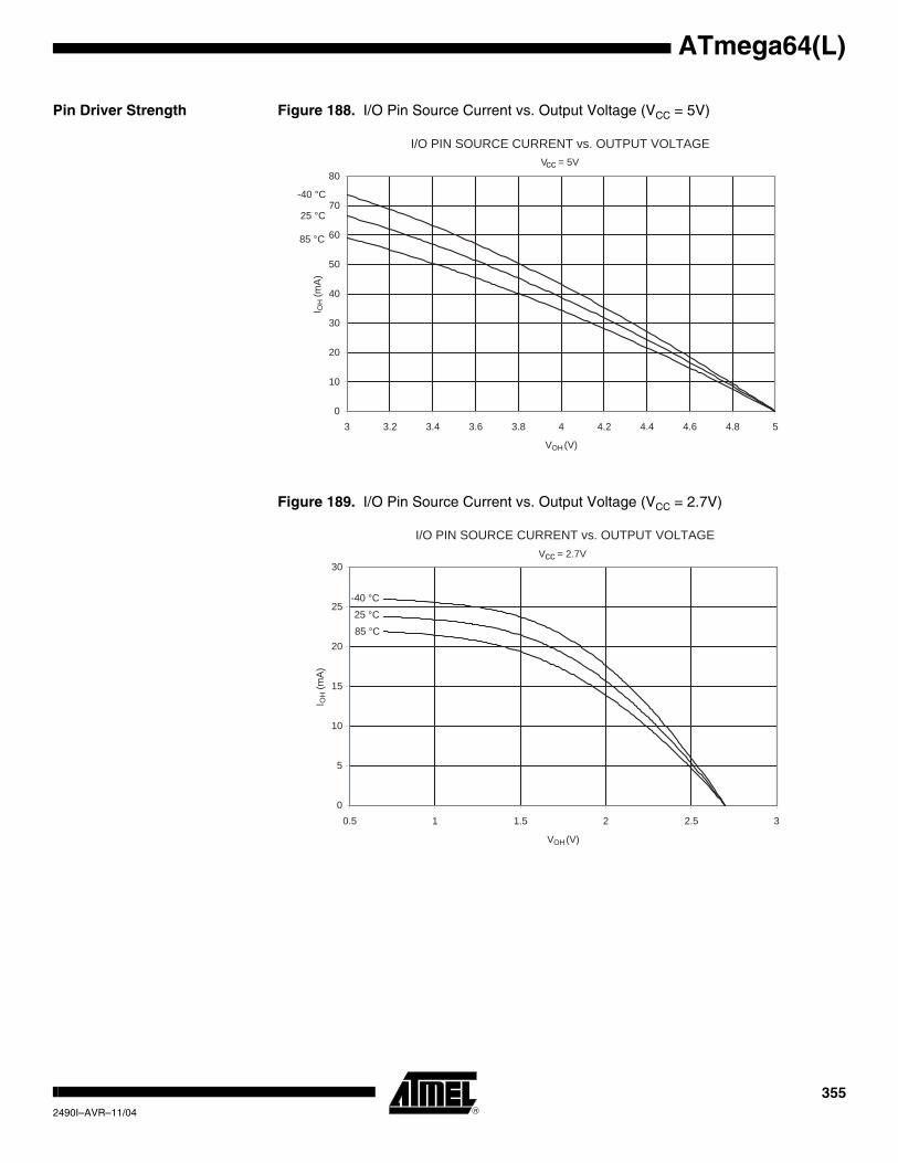
ATmega64(L)
Pin Driver Strength Figure 188. I/O Pin Source Current vs. Output Voltage (VCC = 5V)
Figure 189. I/O Pin Source Current vs. Output Voltage (VCC = 2.7V)
I/O PIN SOURCE CURRENT vs. OUTPUT VOLTAGEVcc = 5V
85 °C
25 °C
-40 °C
0
10
20
30
40
50
60
70
80
3 3.2 3.4 3.6 3.8 4 4.2 4.4 4.6 4.8 5
VOH (V)
I OH
(mA
)
I/O PIN SOURCE CURRENT vs. OUTPUT VOLTAGEVcc = 2.7V
85 °C
25 °C
-40 °C
0
5
10
15
20
25
30
0.5 1 1.5 2 2.5 3
VOH (V)
I OH
(mA
)
3552490I–AVR–11/04
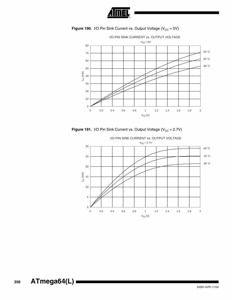
Figure 190. I/O Pin Sink Current vs. Output Voltage (VCC = 5V)
Figure 191. I/O Pin Sink Current vs. Output Voltage (VCC = 2.7V)
I/O PIN SINK CURRENT vs. OUTPUT VOLTAGEVcc = 5V
85 °C
25 °C
-40 °C
0
10
20
30
40
50
60
70
80
0 0.2 0.4 0.6 0.8 1 1.2 1.4 1.6 1.8 2
VOL (V)
I OL (
mA
)
I/O PIN SINK CURRENT vs. OUTPUT VOLTAGEVcc = 2.7V
85 °C
25 °C
-40 °C
0
5
10
15
20
25
30
0 0.2 0.4 0.6 0.8 1 1.2 1.4 1.6 1.8 2
VOL (V)
I OL (
mA
)
356 ATmega64(L)2490I–AVR–11/04
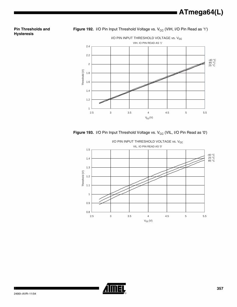
ATmega64(L)
Pin Thresholds and Hysteresis
Figure 192. I/O Pin Input Threshold Voltage vs. VCC (VIH, I/O Pin Read as '1')
Figure 193. I/O Pin Input Threshold Voltage vs. VCC (VIL, I/O Pin Read as '0')
I/O PIN INPUT THRESHOLD VOLTAGE vs. VccVIH. IO PIN READ AS '1'
85 °C25 °C
-40 °C
1
1.2
1.4
1.6
1.8
2
2.2
2.4
2.5 3 3.5 4 4.5 5 5.5
Vcc (V)
Thre
shol
d (V
)
I/O PIN INPUT THRESHOLD VOLTAGE vs. VccVIL. IO PIN READ AS '0'
85 °C25 °C
-40 °C
0.8
0.9
1
1.1
1.2
1.3
1.4
1.5
2.5 3 3.5 4 4.5 5 5.5
Vcc (V)
Thre
shol
d (V
)
3572490I–AVR–11/04
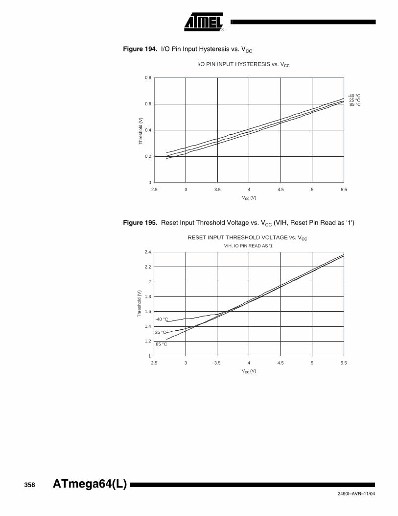
Figure 194. I/O Pin Input Hysteresis vs. VCC
Figure 195. Reset Input Threshold Voltage vs. VCC (VIH, Reset Pin Read as '1')
I/O PIN INPUT HYSTERESIS vs. Vcc
85 °C25 °C
-40 °C
0
0.2
0.4
0.6
0.8
2.5 3 3.5 4 4.5 5 5.5
Vcc (V)
Thre
shol
d (V
)
RESET INPUT THRESHOLD VOLTAGE vs. VccVIH. IO PIN READ AS '1'
85 °C
25 °C
-40 °C
1
1.2
1.4
1.6
1.8
2
2.2
2.4
2.5 3 3.5 4 4.5 5 5.5
Vcc (V)
Thre
shol
d (V
)
358 ATmega64(L)2490I–AVR–11/04
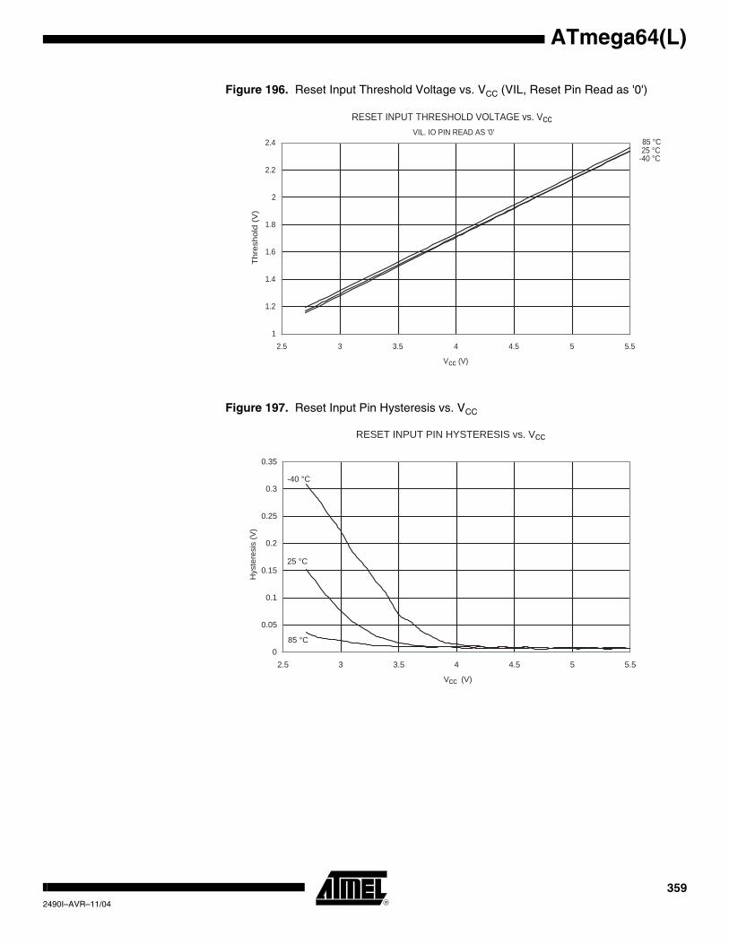
ATmega64(L)
Figure 196. Reset Input Threshold Voltage vs. VCC (VIL, Reset Pin Read as '0')
Figure 197. Reset Input Pin Hysteresis vs. VCC
RESET INPUT THRESHOLD VOLTAGE vs. VccVIL. IO PIN READ AS '0'
85 °C25 °C
-40 °C
1
1.2
1.4
1.6
1.8
2
2.2
2.4
2.5 3 3.5 4 4.5 5 5.5
Vcc (V)
Thr
esho
ld (
V)
RESET INPUT PIN HYSTERESIS vs. Vcc
85 °C
25 °C
-40 °C
0
0.05
0.1
0.15
0.2
0.25
0.3
0.35
2.5 3 3.5 4 4.5 5 5.5
Vcc (V)
Hys
tere
sis
(V)
3592490I–AVR–11/04
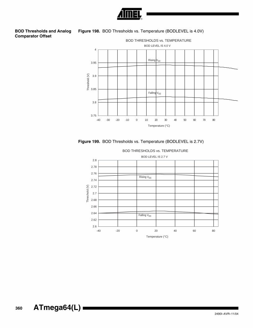
BOD Thresholds and Analog Comparator Offset
Figure 198. BOD Thresholds vs. Temperature (BODLEVEL is 4.0V)
Figure 199. BOD Thresholds vs. Temperature (BODLEVEL is 2.7V)
BOD THRESHOLDS vs. TEMPERATUREBOD LEVEL IS 4.0 V
3.75
3.8
3.85
3.9
3.95
4
-40 -30 -20 -10 0 10 20 30 40 50 60 70 80
Temperature (°C)
Thre
shol
d (V
)
Rising Vcc
Falling Vcc
BOD THRESHOLDS vs. TEMPERATUREBOD LEVEL IS 2.7 V
2.6
2.62
2.64
2.66
2.68
2.7
2.72
2.74
2.76
2.78
2.8
-40 -20 0 20 40 60 80
Temperature (°C)
Thre
sho
ld (V
)
Rising Vcc
Falling Vcc
360 ATmega64(L)2490I–AVR–11/04
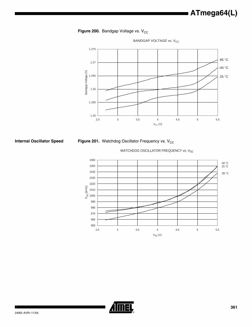
ATmega64(L)
Figure 200. Bandgap Voltage vs. VCC
Internal Oscillator Speed Figure 201. Watchdog Oscillator Frequency vs. VCC
BANDGAP VOLTAGE vs. VCC
85 °C
25 °C
-40 °C
1.25
1.255
1.26
1.265
1.27
1.275
2.5 3 3.5 4 4.5 5 5.5
VCC (V)
Band
gap
Volta
ge (V
)
WATCHDOG OSCILLATOR FREQUENCY vs. Vcc
85 °C
25 °C-40 °C
950
960
970
980
990
1000
1010
1020
1030
1040
1050
1060
2.5 3 3.5 4 4.5 5 5.5
Vcc (V)
F RC
(kH
z)
3612490I–AVR–11/04
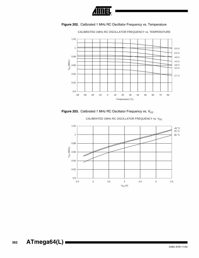
Figure 202. Calibrated 1 MHz RC Oscillator Frequency vs. Temperature
Figure 203. Calibrated 1 MHz RC Oscillator Frequency vs. VCC
CALIBRATED 1MHz RC OSCILLATOR FREQUENCY vs. TEMPERATURE
5.5 V
5.0 V
4.5 V
4.0 V3.6 V3.3 V
2.7 V
0.9
0.92
0.94
0.96
0.98
1
1.02
-40 -30 -20 -10 0 10 20 30 40 50 60 70 80
Temperature (°C)
F RC (
MH
z)
CALIBRATED 1MHz RC OSCILLATOR FREQUENCY vs. Vcc
85 °C
25 °C-40 °C
0.9
0.92
0.94
0.96
0.98
1
1.02
2.5 3 3.5 4 4.5 5 5.5
Vcc (V)
F RC
(MH
z)
362 ATmega64(L)2490I–AVR–11/04

ATmega64(L)
Figure 204. Calibrated 1 MHz RC Oscillator Frequency vs. Osccal Value
Figure 205. Calibrated 2 MHz RC Oscillator Frequency vs. Temperature
CALIBRATED 1MHz RC OSCILLATOR FREQUENCY vs. OSCCAL VALUE
25 °C
0.4
0.5
0.6
0.7
0.8
0.9
1
1.1
1.2
1.3
1.4
1.5
0 16 32 48 64 80 96 112 128 144 160 176 192 208 224 240 256
OSCCAL VALUE
F RC (
MH
z)
CALIBRATED 2MHz RC OSCILLATOR FREQUENCY vs. TEMPERATURE
5.5 V
5.0 V
4.5 V
4.0 V3.6 V3.3 V
2.7 V
1.75
1.8
1.85
1.9
1.95
2
2.05
-40 -30 -20 -10 0 10 20 30 40 50 60 70 80
Temperature (°C)
F RC (M
Hz)
3632490I–AVR–11/04
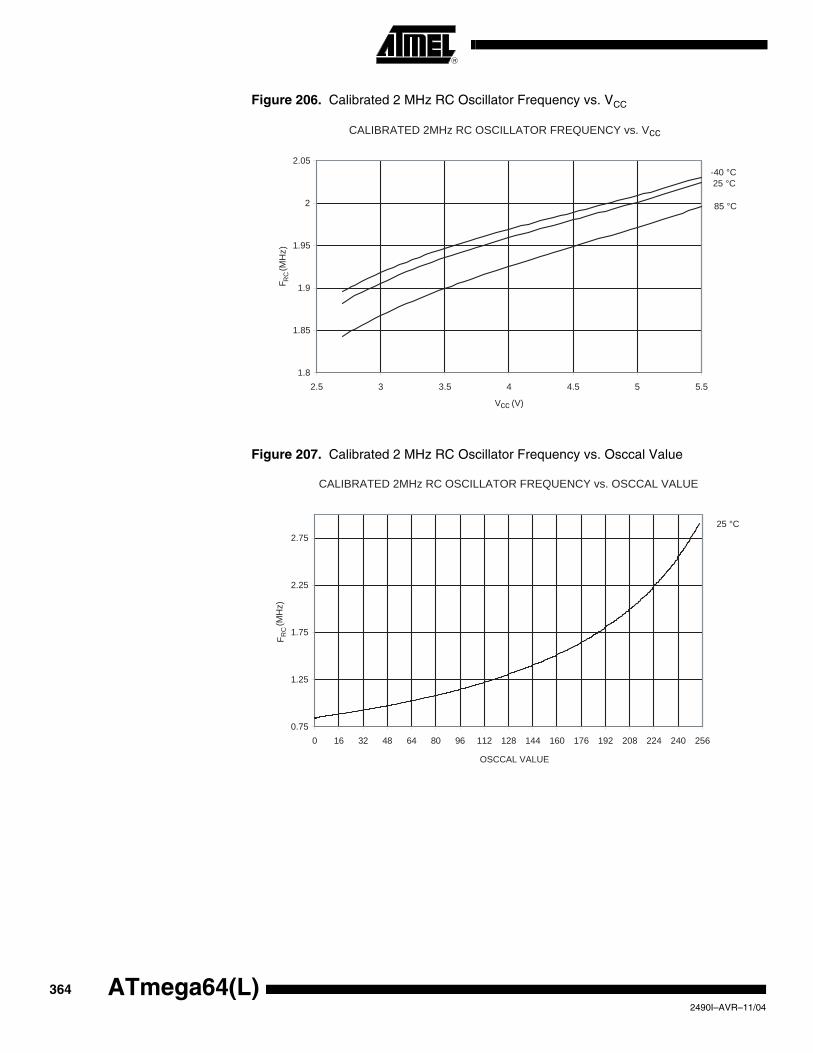
Figure 206. Calibrated 2 MHz RC Oscillator Frequency vs. VCC
Figure 207. Calibrated 2 MHz RC Oscillator Frequency vs. Osccal Value
CALIBRATED 2MHz RC OSCILLATOR FREQUENCY vs. Vcc
85 °C
25 °C-40 °C
1.8
1.85
1.9
1.95
2
2.05
2.5 3 3.5 4 4.5 5 5.5
Vcc (V)
F RC (
MH
z)
CALIBRATED 2MHz RC OSCILLATOR FREQUENCY vs. OSCCAL VALUE
25 °C
0.75
1.25
1.75
2.25
2.75
0 16 32 48 64 80 96 112 128 144 160 176 192 208 224 240 256
OSCCAL VALUE
F RC (
MH
z)
364 ATmega64(L)2490I–AVR–11/04

ATmega64(L)
Figure 208. Calibrated 4 MHz RC Oscillator Frequency vs. Temperature
Figure 209. Calibrated 4 MHz RC Oscillator Frequency vs. VCC
CALIBRATED 4MHz RC OSCILLATOR FREQUENCY vs. TEMPERATURE
5.5 V
5.0 V
4.5 V
4.0 V
3.6 V
3.3 V
2.7 V
3,6
3,65
3,7
3,75
3,8
3,85
3,9
3,95
4
4,05
4,1
-40 -30 -20 -10 0 10 20 30 40 50 60 70 80
Temperature (°C)
F RC
(MH
z)
CALIBRATED 4MHz RC OSCILLATOR FREQUENCY vs. Vcc
85 °C
25 °C-40 °C
3.6
3.65
3.7
3.75
3.8
3.85
3.9
3.95
4
4.05
4.1
2.5 3 3.5 4 4.5 5 5.5
Vcc (V)
F RC
(MH
z)
3652490I–AVR–11/04
Figure 210. Calibrated 4 MHz RC Oscillator Frequency vs. Osccal Value
Figure 211. Calibrated 8 MHz RC Oscillator Frequency vs. Temperature
CALIBRATED 4MHz RC OSCILLATOR FREQUENCY vs. OSCCAL VALUE
25 °C
1.5
2
2.5
3
3.5
4
4.5
5
5.5
6
6.5
0 16 32 48 64 80 96 112 128 144 160 176 192 208 224 240 256
OSCCAL VALUE
F RC
(MH
z)
CALIBRATED 8MHz RC OSCILLATOR FREQUENCY vs. TEMPERATURE
5.5 V5.0 V4.5 V
4.0 V
3.6 V
3.3 V
2.7 V
6.5
6.7
6.9
7.1
7.3
7.5
7.7
7.9
8.1
8.3
-40 -20 0 20 40 60 80
Temperature (°C)
F RC
(MH
z)
366 ATmega64(L)2490I–AVR–11/04
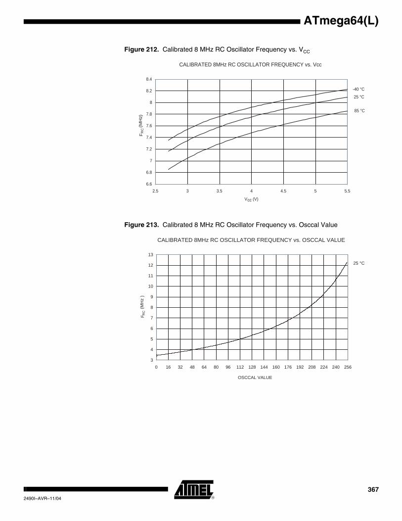
ATmega64(L)
Figure 212. Calibrated 8 MHz RC Oscillator Frequency vs. VCC
Figure 213. Calibrated 8 MHz RC Oscillator Frequency vs. Osccal Value
CALIBRATED 8MHz RC OSCILLATOR FREQUENCY vs. Vcc
85 °C
25 °C
-40 °C
6.6
6.8
7
7.2
7.4
7.6
7.8
8
8.2
8.4
2.5 3 3.5 4 4.5 5 5.5
Vcc (V)
F RC
(MH
z)
CALIBRATED 8MHz RC OSCILLATOR FREQUENCY vs. OSCCAL VALUE
25 °C
3
4
5
6
7
8
9
10
11
12
13
0 16 32 48 64 80 96 112 128 144 160 176 192 208 224 240 256
OSCCAL VALUE
F RC
(MH
z)
3672490I–AVR–11/04
Current Consumption of Peripheral Units
Figure 214. Brownout Detector Current vs. VCC
Figure 215. ADC Current vs. VCC (ADC CLK = 50 kHz)
BROWNOUT DETECTOR CURRENT vs. Vcc
85 °C
25 °C
-40 °C
0
2
4
6
8
10
12
14
16
2.5 3 3.5 4 4.5 5 5.5
Vcc (V)
I cc
(uA
)
ADC CURRENT vs. VccADC CLK = 50KHz
85 °C
25 °C
-40 °C
130
150
170
190
210
230
250
270
290
310
330
2.5 3 3.5 4 4.5 5 5.5
Vcc (V)
I cc
(uA
)
368 ATmega64(L)2490I–AVR–11/04
ATmega64(L)
Figure 216. Aref Current vs. VCC
Figure 217. Analog Comparator Current vs. VCC
AREF CURRENT vs. Vcc
85 °C25 °C
-40 °C
70
80
90
100
110
120
130
140
150
160
170
2.5 3 3.5 4 4.5 5 5.5
Vcc (V)
I cc
(uA
)
ANALOG COMPARATOR CURRENT vs. Vcc
85 °C
25 °C
-40 °C
30
40
50
60
70
80
90
2,5 3 3,5 4 4,5 5 5,5
Vcc (V)
I cc
(uA
)
3692490I–AVR–11/04
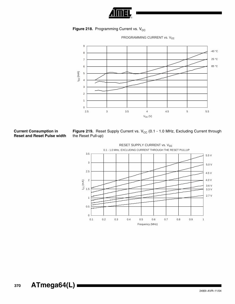
Figure 218. Programming Current vs. VCC
Current Consumption in Reset and Reset Pulse width
Figure 219. Reset Supply Current vs. VCC (0.1 - 1.0 MHz, Excluding Current throughthe Reset Pull-up)
PROGRAMMING CURRENT vs. Vcc
85 °C
25 °C
-40 °C
0
1
2
3
4
5
6
7
8
9
2.5 3 3.5 4 4.5 5 5.5
Vcc (V)
I cc
(mA
)
RESET SUPPLY CURRENT vs. Vcc0.1 - 1.0 MHz. EXCLUDING CURRENT THROUGH THE RESET PULLUP
5.5 V
5.0 V
4.5 V
4.0 V
3.6 V3.3 V
2.7 V
0
0.5
1
1.5
2
2.5
3
3.5
0.1 0.2 0.3 0.4 0.5 0.6 0.7 0.8 0.9 1
Frequency (MHz)
I CC
(mA
)
370 ATmega64(L)2490I–AVR–11/04
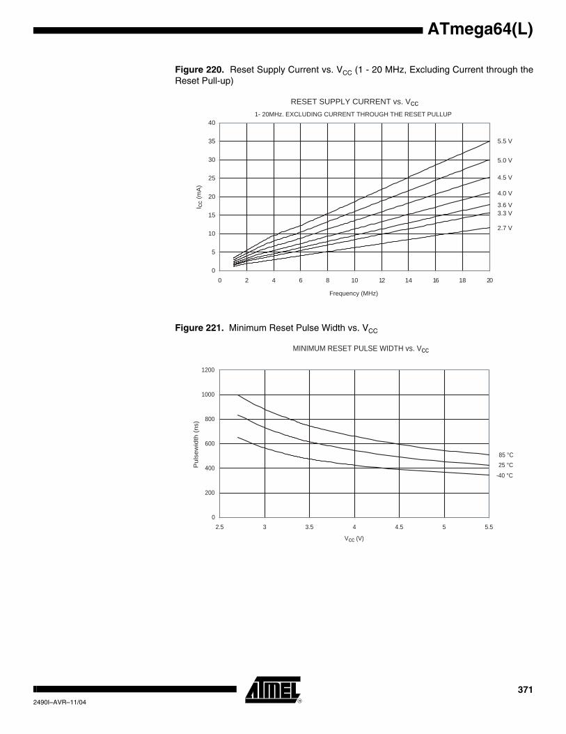
ATmega64(L)
Figure 220. Reset Supply Current vs. VCC (1 - 20 MHz, Excluding Current through theReset Pull-up)
Figure 221. Minimum Reset Pulse Width vs. VCC
RESET SUPPLY CURRENT vs. Vcc1- 20MHz. EXCLUDING CURRENT THROUGH THE RESET PULLUP
5.5 V
5.0 V
4.5 V
4.0 V
3.6 V3.3 V
2.7 V
0
5
10
15
20
25
30
35
40
0 2 4 6 8 10 12 14 16 18 20
Frequency (MHz)
I cc
(mA
)
MINIMUM RESET PULSE WIDTH vs. Vcc
85 °C25 °C
-40 °C
0
200
400
600
800
1000
1200
2.5 3 3.5 4 4.5 5 5.5
Vcc (V)
Pul
sew
idth
(ns
)
3712490I–AVR–11/04
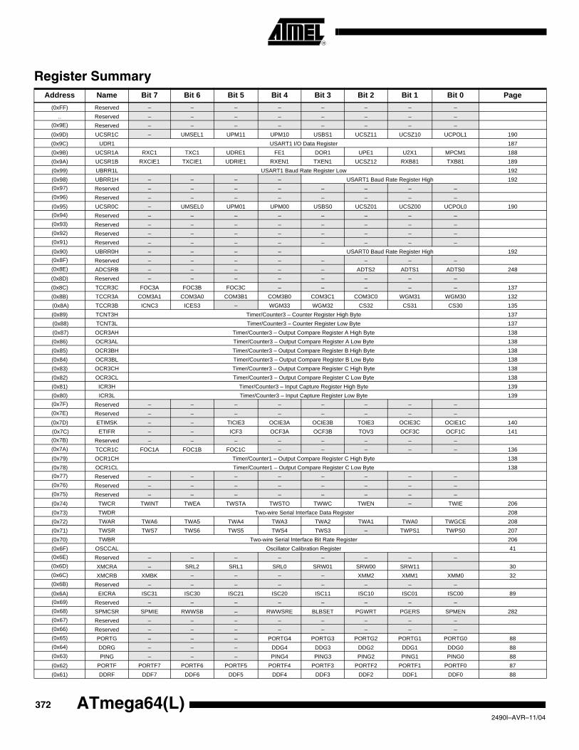
Register Summary Address Name Bit 7 Bit 6 Bit 5 Bit 4 Bit 3 Bit 2 Bit 1 Bit 0 Page
(0xFF) Reserved – – – – – – – –.. Reserved – – – – – – – –
(0x9E) Reserved – – – – – – – –(0x9D) UCSR1C – UMSEL1 UPM11 UPM10 USBS1 UCSZ11 UCSZ10 UCPOL1 190(0x9C) UDR1 USART1 I/O Data Register 187(0x9B) UCSR1A RXC1 TXC1 UDRE1 FE1 DOR1 UPE1 U2X1 MPCM1 188(0x9A) UCSR1B RXCIE1 TXCIE1 UDRIE1 RXEN1 TXEN1 UCSZ12 RXB81 TXB81 189(0x99) UBRR1L USART1 Baud Rate Register Low 192(0x98) UBRR1H – – – – USART1 Baud Rate Register High 192(0x97) Reserved – – – – – – – –(0x96) Reserved – – – – – – – –(0x95) UCSR0C – UMSEL0 UPM01 UPM00 USBS0 UCSZ01 UCSZ00 UCPOL0 190(0x94) Reserved – – – – – – – –(0x93) Reserved – – – – – – – –(0x92) Reserved – – – – – – – –(0x91) Reserved – – – – – – – –(0x90) UBRR0H – – – – USART0 Baud Rate Register High 192(0x8F) Reserved – – – – – – – –(0x8E) ADCSRB – – – – – ADTS2 ADTS1 ADTS0 248(0x8D) Reserved – – – – – – – –(0x8C) TCCR3C FOC3A FOC3B FOC3C – – – – – 137(0x8B) TCCR3A COM3A1 COM3A0 COM3B1 COM3B0 COM3C1 COM3C0 WGM31 WGM30 132 (0x8A) TCCR3B ICNC3 ICES3 – WGM33 WGM32 CS32 CS31 CS30 135(0x89) TCNT3H Timer/Counter3 – Counter Register High Byte 137 (0x88) TCNT3L Timer/Counter3 – Counter Register Low Byte 137 (0x87) OCR3AH Timer/Counter3 – Output Compare Register A High Byte 138(0x86) OCR3AL Timer/Counter3 – Output Compare Register A Low Byte 138(0x85) OCR3BH Timer/Counter3 – Output Compare Register B High Byte 138(0x84) OCR3BL Timer/Counter3 – Output Compare Register B Low Byte 138(0x83) OCR3CH Timer/Counter3 – Output Compare Register C High Byte 138(0x82) OCR3CL Timer/Counter3 – Output Compare Register C Low Byte 138(0x81) ICR3H Timer/Counter3 – Input Capture Register High Byte 139(0x80) ICR3L Timer/Counter3 – Input Capture Register Low Byte 139(0x7F) Reserved – – – – – – – –(0x7E) Reserved – – – – – – – –(0x7D) ETIMSK – – TICIE3 OCIE3A OCIE3B TOIE3 OCIE3C OCIE1C 140 (0x7C) ETIFR – – ICF3 OCF3A OCF3B TOV3 OCF3C OCF1C 141(0x7B) Reserved – – – – – – – –(0x7A) TCCR1C FOC1A FOC1B FOC1C – – – – – 136(0x79) OCR1CH Timer/Counter1 – Output Compare Register C High Byte 138(0x78) OCR1CL Timer/Counter1 – Output Compare Register C Low Byte 138(0x77) Reserved – – – – – – – –(0x76) Reserved – – – – – – – –(0x75) Reserved – – – – – – – –(0x74) TWCR TWINT TWEA TWSTA TWSTO TWWC TWEN – TWIE 206(0x73) TWDR Two-wire Serial Interface Data Register 208(0x72) TWAR TWA6 TWA5 TWA4 TWA3 TWA2 TWA1 TWA0 TWGCE 208(0x71) TWSR TWS7 TWS6 TWS5 TWS4 TWS3 – TWPS1 TWPS0 207(0x70) TWBR Two-wire Serial Interface Bit Rate Register 206(0x6F) OSCCAL Oscillator Calibration Register 41(0x6E) Reserved – – – – – – – –(0x6D) XMCRA – SRL2 SRL1 SRL0 SRW01 SRW00 SRW11 30(0x6C) XMCRB XMBK – – – – XMM2 XMM1 XMM0 32(0x6B) Reserved – – – – – – – –(0x6A) EICRA ISC31 ISC30 ISC21 ISC20 ISC11 ISC10 ISC01 ISC00 89(0x69) Reserved – – – – – – – –(0x68) SPMCSR SPMIE RWWSB – RWWSRE BLBSET PGWRT PGERS SPMEN 282(0x67) Reserved – – – – – – – –(0x66) Reserved – – – – – – – –(0x65) PORTG – – – PORTG4 PORTG3 PORTG2 PORTG1 PORTG0 88(0x64) DDRG – – – DDG4 DDG3 DDG2 DDG1 DDG0 88(0x63) PING – – – PING4 PING3 PING2 PING1 PING0 88(0x62) PORTF PORTF7 PORTF6 PORTF5 PORTF4 PORTF3 PORTF2 PORTF1 PORTF0 87(0x61) DDRF DDF7 DDF6 DDF5 DDF4 DDF3 DDF2 DDF1 DDF0 88
372 ATmega64(L)2490I–AVR–11/04
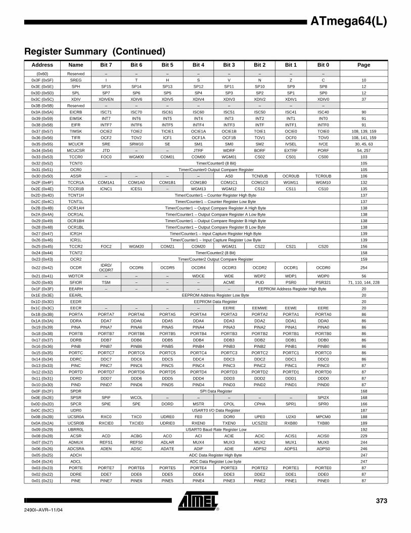
ATmega64(L)
(0x60) Reserved – – – – – – – –0x3F (0x5F) SREG I T H S V N Z C 100x3E (0x5E) SPH SP15 SP14 SP13 SP12 SP11 SP10 SP9 SP8 120x3D (0x5D) SPL SP7 SP6 SP5 SP4 SP3 SP2 SP1 SP0 120x3C (0x5C) XDIV XDIVEN XDIV6 XDIV5 XDIV4 XDIV3 XDIV2 XDIV1 XDIV0 370x3B (0x5B) Reserved – – – – – – – –0x3A (0x5A) EICRB ISC71 ISC70 ISC61 ISC60 ISC51 ISC50 ISC41 ISC40 900x39 (0x59) EIMSK INT7 INT6 INT5 INT4 INT3 INT2 INT1 INT0 910x38 (0x58) EIFR INTF7 INTF6 INTF5 INTF4 INTF3 INTF INTF1 INTF0 910x37 (0x57) TIMSK OCIE2 TOIE2 TICIE1 OCIE1A OCIE1B TOIE1 OCIE0 TOIE0 108, 139, 1590x36 (0x56) TIFR OCF2 TOV2 ICF1 OCF1A OCF1B TOV1 OCF0 TOV0 108, 141, 1590x35 (0x55) MCUCR SRE SRW10 SE SM1 SM0 SM2 IVSEL IVCE 30, 45, 63 0x34 (0x54) MCUCSR JTD – – JTRF WDRF BORF EXTRF PORF 54, 2570x33 (0x53) TCCR0 FOC0 WGM00 COM01 COM00 WGM01 CS02 CS01 CS00 1030x32 (0x52) TCNT0 Timer/Counter0 (8 Bit) 1050x31 (0x51) OCR0 Timer/Counter0 Output Compare Register 1050x30 (0x50) ASSR – – – – AS0 TCN0UB OCR0UB TCR0UB 1060x2F (0x4F) TCCR1A COM1A1 COM1A0 COM1B1 COM1B0 COM1C1 COM1C0 WGM11 WGM10 1320x2E (0x4E) TCCR1B ICNC1 ICES1 – WGM13 WGM12 CS12 CS11 CS10 1350x2D (0x4D) TCNT1H Timer/Counter1 – Counter Register High Byte 1370x2C (0x4C) TCNT1L Timer/Counter1 – Counter Register Low Byte 1370x2B (0x4B) OCR1AH Timer/Counter1 – Output Compare Register A High Byte 1380x2A (0x4A) OCR1AL Timer/Counter1 – Output Compare Register A Low Byte 1380x29 (0x49) OCR1BH Timer/Counter1 – Output Compare Register B High Byte 1380x28 (0x48) OCR1BL Timer/Counter1 – Output Compare Register B Low Byte 1380x27 (0x47) ICR1H Timer/Counter1 – Input Capture Register High Byte 1390x26 (0x46) ICR1L Timer/Counter1 – Input Capture Register Low Byte 1390x25 (0x45) TCCR2 FOC2 WGM20 COM21 COM20 WGM21 CS22 CS21 CS20 1560x24 (0x44) TCNT2 Timer/Counter2 (8 Bit) 1580x23 (0x43) OCR2 Timer/Counter2 Output Compare Register 159
0x22 (0x42) OCDR IDRD/OCDR7 OCDR6 OCDR5 OCDR4 OCDR3 OCDR2 OCDR1 OCDR0 254
0x21 (0x41) WDTCR – – – WDCE WDE WDP2 WDP1 WDP0 560x20 (0x40) SFIOR TSM – – – ACME PUD PSR0 PSR321 71, 110, 144, 2280x1F (0x3F) EEARH – – – – – EEPROM Address Register High Byte 200x1E (0x3E) EEARL EEPROM Address Register Low Byte 200x1D (0x3D) EEDR EEPROM Data Register 200x1C (0x3C) EECR – – – – EERIE EEMWE EEWE EERE 200x1B (0x3B) PORTA PORTA7 PORTA6 PORTA5 PORTA4 PORTA3 PORTA2 PORTA1 PORTA0 860x1A (0x3A) DDRA DDA7 DDA6 DDA5 DDA4 DDA3 DDA2 DDA1 DDA0 860x19 (0x39) PINA PINA7 PINA6 PINA5 PINA4 PINA3 PINA2 PINA1 PINA0 860x18 (0x38) PORTB PORTB7 PORTB6 PORTB5 PORTB4 PORTB3 PORTB2 PORTB1 PORTB0 860x17 (0x37) DDRB DDB7 DDB6 DDB5 DDB4 DDB3 DDB2 DDB1 DDB0 860x16 (0x36) PINB PINB7 PINB6 PINB5 PINB4 PINB3 PINB2 PINB1 PINB0 860x15 (0x35) PORTC PORTC7 PORTC6 PORTC5 PORTC4 PORTC3 PORTC2 PORTC1 PORTC0 860x14 (0x34) DDRC DDC7 DDC6 DDC5 DDC4 DDC3 DDC2 DDC1 DDC0 860x13 (0x33) PINC PINC7 PINC6 PINC5 PINC4 PINC3 PINC2 PINC1 PINC0 870x12 (0x32) PORTD PORTD7 PORTD6 PORTD5 PORTD4 PORTD3 PORTD2 PORTD1 PORTD0 870x11 (0x31) DDRD DDD7 DDD6 DDD5 DDD4 DDD3 DDD2 DDD1 DDD0 870x10 (0x30) PIND PIND7 PIND6 PIND5 PIND4 PIND3 PIND2 PIND1 PIND0 870x0F (0x2F) SPDR SPI Data Register 1680x0E (0x2E) SPSR SPIF WCOL – – – – – SPI2X 1680x0D (0x2D) SPCR SPIE SPE DORD MSTR CPOL CPHA SPR1 SPR0 1660x0C (0x2C) UDR0 USART0 I/O Data Register 1870x0B (0x2B) UCSR0A RXC0 TXC0 UDRE0 FE0 DOR0 UPE0 U2X0 MPCM0 1880x0A (0x2A) UCSR0B RXCIE0 TXCIE0 UDRIE0 RXEN0 TXEN0 UCSZ02 RXB80 TXB80 1890x09 (0x29) UBRR0L USART0 Baud Rate Register Low 1920x08 (0x28) ACSR ACD ACBG ACO ACI ACIE ACIC ACIS1 ACIS0 2290x07 (0x27) ADMUX REFS1 REFS0 ADLAR MUX4 MUX3 MUX2 MUX1 MUX0 2440x06 (0x26) ADCSRA ADEN ADSC ADATE ADIF ADIE ADPS2 ADPS1 ADPS0 2460x05 (0x25) ADCH ADC Data Register High Byte 2470x04 (0x24) ADCL ADC Data Register Low byte 2470x03 (0x23) PORTE PORTE7 PORTE6 PORTE5 PORTE4 PORTE3 PORTE2 PORTE1 PORTE0 870x02 (0x22) DDRE DDE7 DDE6 DDE5 DDE4 DDE3 DDE2 DDE1 DDE0 870x01 (0x21) PINE PINE7 PINE6 PINE5 PINE4 PINE3 PINE2 PINE1 PINE0 87
Register Summary (Continued)Address Name Bit 7 Bit 6 Bit 5 Bit 4 Bit 3 Bit 2 Bit 1 Bit 0 Page
3732490I–AVR–11/04

Notes: 1. For compatibility with future devices, reserved bits should be written to zero if accessed. Reserved I/O memory addressesshould never be written.
2. Some of the status flags are cleared by writing a logical one to them. Note that the CBI and SBI instructions will operate onall bits in the I/O Register, writing a one back into any flag read as set, thus clearing the flag. The CBI and SBI instructionswork with registers 0x00 to 0x1F only.
0x00 (0x20) PINF PINF7 PINF6 PINF5 PINF4 PINF3 PINF2 PINF1 PINF0 88
Register Summary (Continued)Address Name Bit 7 Bit 6 Bit 5 Bit 4 Bit 3 Bit 2 Bit 1 Bit 0 Page
374 ATmega64(L)2490I–AVR–11/04
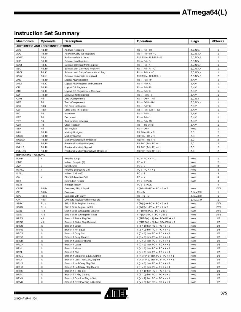
ATmega64(L)
Instruction Set Summary Mnemonics Operands Description Operation Flags #ClocksARITHMETIC AND LOGIC INSTRUCTIONSADD Rd, Rr Add two Registers Rd ← Rd + Rr Z,C,N,V,H 1ADC Rd, Rr Add with Carry two Registers Rd ← Rd + Rr + C Z,C,N,V,H 1ADIW Rdl,K Add Immediate to Word Rdh:Rdl ← Rdh:Rdl + K Z,C,N,V,S 2SUB Rd, Rr Subtract two Registers Rd ← Rd - Rr Z,C,N,V,H 1SUBI Rd, K Subtract Constant from Register Rd ← Rd - K Z,C,N,V,H 1SBC Rd, Rr Subtract with Carry two Registers Rd ← Rd - Rr - C Z,C,N,V,H 1SBCI Rd, K Subtract with Carry Constant from Reg. Rd ← Rd - K - C Z,C,N,V,H 1SBIW Rdl,K Subtract Immediate from Word Rdh:Rdl ← Rdh:Rdl - K Z,C,N,V,S 2AND Rd, Rr Logical AND Registers Rd ← Rd • Rr Z,N,V 1ANDI Rd, K Logical AND Register and Constant Rd ← Rd • K Z,N,V 1OR Rd, Rr Logical OR Registers Rd ← Rd v Rr Z,N,V 1ORI Rd, K Logical OR Register and Constant Rd ← Rd v K Z,N,V 1EOR Rd, Rr Exclusive OR Registers Rd ← Rd ⊕ Rr Z,N,V 1COM Rd One’s Complement Rd ← 0xFF − Rd Z,C,N,V 1NEG Rd Two’s Complement Rd ← 0x00 − Rd Z,C,N,V,H 1SBR Rd,K Set Bit(s) in Register Rd ← Rd v K Z,N,V 1CBR Rd,K Clear Bit(s) in Register Rd ← Rd • (0xFF - K) Z,N,V 1INC Rd Increment Rd ← Rd + 1 Z,N,V 1DEC Rd Decrement Rd ← Rd − 1 Z,N,V 1TST Rd Test for Zero or Minus Rd ← Rd • Rd Z,N,V 1CLR Rd Clear Register Rd ← Rd ⊕ Rd Z,N,V 1SER Rd Set Register Rd ← 0xFF None 1MUL Rd, Rr Multiply Unsigned R1:R0 ← Rd x Rr Z,C 2MULS Rd, Rr Multiply Signed R1:R0 ← Rd x Rr Z,C 2MULSU Rd, Rr Multiply Signed with Unsigned R1:R0 ← Rd x Rr Z,C 2FMUL Rd, Rr Fractional Multiply Unsigned R1:R0 ¨ (Rd x Rr) << 1 Z,C 2FMULS Rd, Rr Fractional Multiply Signed R1:R0 ¨ (Rd x Rr) << 1 Z,C 2FMULSU Rd, Rr Fractional Multiply Signed with Unsigned R1:R0 ¨ (Rd x Rr) << 1 Z,C 2BRANCH INSTRUCTIONSRJMP k Relative Jump PC ← PC + k + 1 None 2IJMP Indirect Jump to (Z) PC ← Z None 2JMP k Direct Jump PC ← k None 3RCALL k Relative Subroutine Call PC ← PC + k + 1 None 3ICALL Indirect Call to (Z) PC ← Z None 3CALL k Direct Subroutine Call PC ← k None 4RET Subroutine Return PC ← STACK None 4RETI Interrupt Return PC ← STACK I 4CPSE Rd,Rr Compare, Skip if Equal if (Rd = Rr) PC ← PC + 2 or 3 None 1/2/3CP Rd,Rr Compare Rd − Rr Z, N,V,C,H 1 CPC Rd,Rr Compare with Carry Rd − Rr − C Z, N,V,C,H 1CPI Rd,K Compare Register with Immediate Rd − K Z, N,V,C,H 1SBRC Rr, b Skip if Bit in Register Cleared if (Rr(b)=0) PC ← PC + 2 or 3 None 1/2/3SBRS Rr, b Skip if Bit in Register is Set if (Rr(b)=1) PC ← PC + 2 or 3 None 1/2/3SBIC P, b Skip if Bit in I/O Register Cleared if (P(b)=0) PC ← PC + 2 or 3 None 1/2/3SBIS P, b Skip if Bit in I/O Register is Set if (P(b)=1) PC ← PC + 2 or 3 None 1/2/3BRBS s, k Branch if Status Flag Set if (SREG(s) = 1) then PC←PC+k + 1 None 1/2BRBC s, k Branch if Status Flag Cleared if (SREG(s) = 0) then PC←PC+k + 1 None 1/2BREQ k Branch if Equal if (Z = 1) then PC ← PC + k + 1 None 1/2BRNE k Branch if Not Equal if (Z = 0) then PC ← PC + k + 1 None 1/2BRCS k Branch if Carry Set if (C = 1) then PC ← PC + k + 1 None 1/2BRCC k Branch if Carry Cleared if (C = 0) then PC ← PC + k + 1 None 1/2BRSH k Branch if Same or Higher if (C = 0) then PC ← PC + k + 1 None 1/2BRLO k Branch if Lower if (C = 1) then PC ← PC + k + 1 None 1/2BRMI k Branch if Minus if (N = 1) then PC ← PC + k + 1 None 1/2BRPL k Branch if Plus if (N = 0) then PC ← PC + k + 1 None 1/2BRGE k Branch if Greater or Equal, Signed if (N ⊕ V= 0) then PC ← PC + k + 1 None 1/2BRLT k Branch if Less Than Zero, Signed if (N ⊕ V= 1) then PC ← PC + k + 1 None 1/2BRHS k Branch if Half Carry Flag Set if (H = 1) then PC ← PC + k + 1 None 1/2BRHC k Branch if Half Carry Flag Cleared if (H = 0) then PC ← PC + k + 1 None 1/2BRTS k Branch if T Flag Set if (T = 1) then PC ← PC + k + 1 None 1/2BRTC k Branch if T Flag Cleared if (T = 0) then PC ← PC + k + 1 None 1/2BRVS k Branch if Overflow Flag is Set if (V = 1) then PC ← PC + k + 1 None 1/2BRVC k Branch if Overflow Flag is Cleared if (V = 0) then PC ← PC + k + 1 None 1/2
3752490I–AVR–11/04
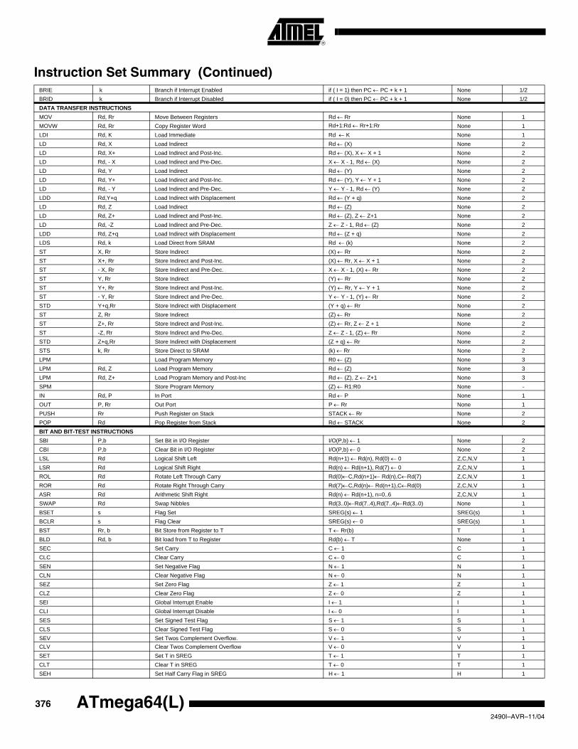
BRIE k Branch if Interrupt Enabled if ( I = 1) then PC ← PC + k + 1 None 1/2BRID k Branch if Interrupt Disabled if ( I = 0) then PC ← PC + k + 1 None 1/2DATA TRANSFER INSTRUCTIONSMOV Rd, Rr Move Between Registers Rd ← Rr None 1MOVW Rd, Rr Copy Register Word Rd+1:Rd ← Rr+1:Rr None 1LDI Rd, K Load Immediate Rd ← K None 1LD Rd, X Load Indirect Rd ← (X) None 2LD Rd, X+ Load Indirect and Post-Inc. Rd ← (X), X ← X + 1 None 2LD Rd, - X Load Indirect and Pre-Dec. X ← X - 1, Rd ← (X) None 2LD Rd, Y Load Indirect Rd ← (Y) None 2LD Rd, Y+ Load Indirect and Post-Inc. Rd ← (Y), Y ← Y + 1 None 2LD Rd, - Y Load Indirect and Pre-Dec. Y ← Y - 1, Rd ← (Y) None 2LDD Rd,Y+q Load Indirect with Displacement Rd ← (Y + q) None 2LD Rd, Z Load Indirect Rd ← (Z) None 2LD Rd, Z+ Load Indirect and Post-Inc. Rd ← (Z), Z ← Z+1 None 2LD Rd, -Z Load Indirect and Pre-Dec. Z ← Z - 1, Rd ← (Z) None 2LDD Rd, Z+q Load Indirect with Displacement Rd ← (Z + q) None 2LDS Rd, k Load Direct from SRAM Rd ← (k) None 2ST X, Rr Store Indirect (X) ← Rr None 2ST X+, Rr Store Indirect and Post-Inc. (X) ← Rr, X ← X + 1 None 2ST - X, Rr Store Indirect and Pre-Dec. X ← X - 1, (X) ← Rr None 2ST Y, Rr Store Indirect (Y) ← Rr None 2ST Y+, Rr Store Indirect and Post-Inc. (Y) ← Rr, Y ← Y + 1 None 2ST - Y, Rr Store Indirect and Pre-Dec. Y ← Y - 1, (Y) ← Rr None 2STD Y+q,Rr Store Indirect with Displacement (Y + q) ← Rr None 2ST Z, Rr Store Indirect (Z) ← Rr None 2ST Z+, Rr Store Indirect and Post-Inc. (Z) ← Rr, Z ← Z + 1 None 2ST -Z, Rr Store Indirect and Pre-Dec. Z ← Z - 1, (Z) ← Rr None 2STD Z+q,Rr Store Indirect with Displacement (Z + q) ← Rr None 2STS k, Rr Store Direct to SRAM (k) ← Rr None 2LPM Load Program Memory R0 ← (Z) None 3LPM Rd, Z Load Program Memory Rd ← (Z) None 3LPM Rd, Z+ Load Program Memory and Post-Inc Rd ← (Z), Z ← Z+1 None 3SPM Store Program Memory (Z) ← R1:R0 None -IN Rd, P In Port Rd ← P None 1OUT P, Rr Out Port P ← Rr None 1PUSH Rr Push Register on Stack STACK ← Rr None 2POP Rd Pop Register from Stack Rd ← STACK None 2BIT AND BIT-TEST INSTRUCTIONSSBI P,b Set Bit in I/O Register I/O(P,b) ← 1 None 2CBI P,b Clear Bit in I/O Register I/O(P,b) ← 0 None 2LSL Rd Logical Shift Left Rd(n+1) ← Rd(n), Rd(0) ← 0 Z,C,N,V 1LSR Rd Logical Shift Right Rd(n) ← Rd(n+1), Rd(7) ← 0 Z,C,N,V 1ROL Rd Rotate Left Through Carry Rd(0)←C,Rd(n+1)← Rd(n),C←Rd(7) Z,C,N,V 1ROR Rd Rotate Right Through Carry Rd(7)←C,Rd(n)← Rd(n+1),C←Rd(0) Z,C,N,V 1ASR Rd Arithmetic Shift Right Rd(n) ← Rd(n+1), n=0..6 Z,C,N,V 1SWAP Rd Swap Nibbles Rd(3..0)←Rd(7..4),Rd(7..4)←Rd(3..0) None 1BSET s Flag Set SREG(s) ← 1 SREG(s) 1BCLR s Flag Clear SREG(s) ← 0 SREG(s) 1BST Rr, b Bit Store from Register to T T ← Rr(b) T 1BLD Rd, b Bit load from T to Register Rd(b) ← T None 1SEC Set Carry C ← 1 C 1CLC Clear Carry C ← 0 C 1SEN Set Negative Flag N ← 1 N 1CLN Clear Negative Flag N ← 0 N 1SEZ Set Zero Flag Z ← 1 Z 1CLZ Clear Zero Flag Z ← 0 Z 1SEI Global Interrupt Enable I ← 1 I 1CLI Global Interrupt Disable I ← 0 I 1SES Set Signed Test Flag S ← 1 S 1CLS Clear Signed Test Flag S ← 0 S 1SEV Set Twos Complement Overflow. V ← 1 V 1CLV Clear Twos Complement Overflow V ← 0 V 1SET Set T in SREG T ← 1 T 1CLT Clear T in SREG T ← 0 T 1SEH Set Half Carry Flag in SREG H ← 1 H 1
Instruction Set Summary (Continued)
376 ATmega64(L)2490I–AVR–11/04
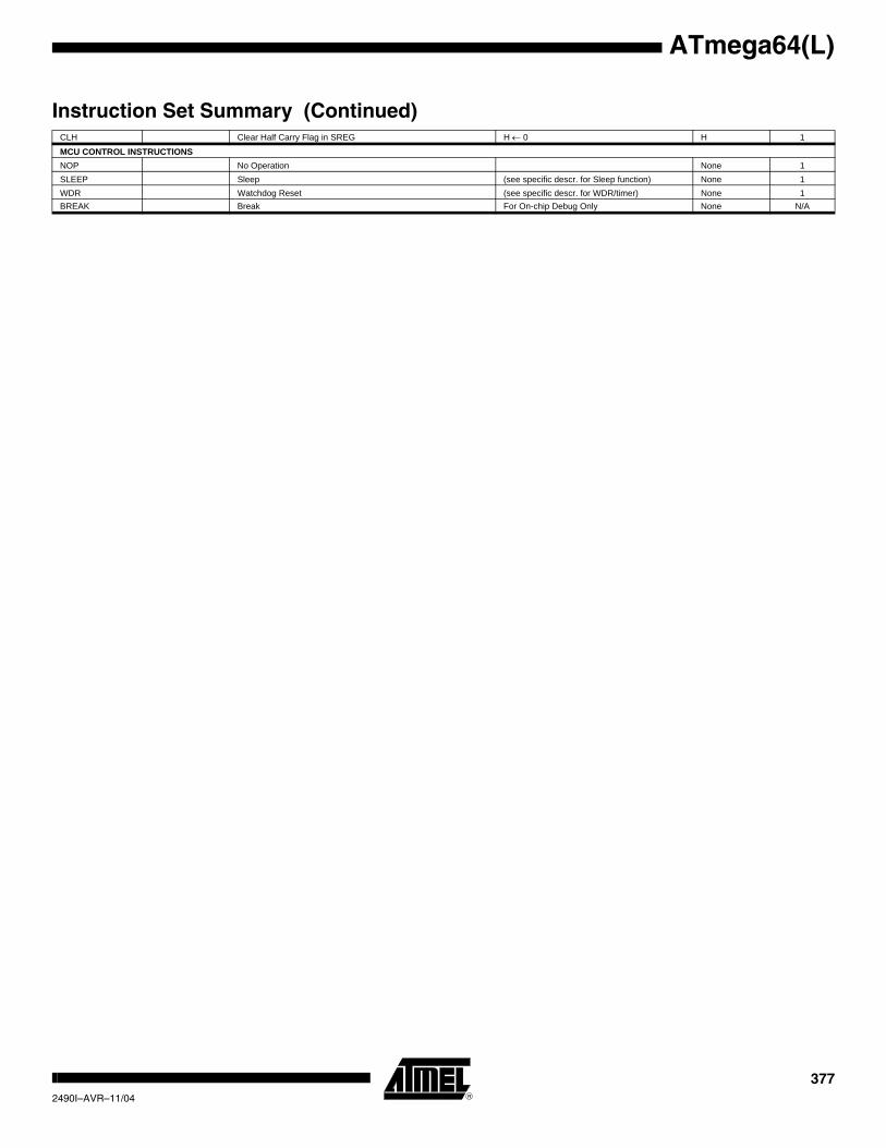
ATmega64(L)
CLH Clear Half Carry Flag in SREG H ← 0 H 1
MCU CONTROL INSTRUCTIONSNOP No Operation None 1SLEEP Sleep (see specific descr. for Sleep function) None 1WDR Watchdog Reset (see specific descr. for WDR/timer) None 1BREAK Break For On-chip Debug Only None N/A
Instruction Set Summary (Continued)
3772490I–AVR–11/04
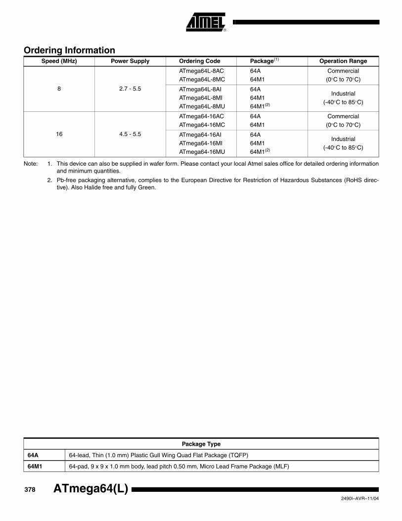
Ordering Information
Note: 1. This device can also be supplied in wafer form. Please contact your local Atmel sales office for detailed ordering informationand minimum quantities.
2. Pb-free packaging alternative, complies to the European Directive for Restriction of Hazardous Substances (RoHS direc-tive). Also Halide free and fully Green.
Speed (MHz) Power Supply Ordering Code Package(1) Operation Range
8 2.7 - 5.5
ATmega64L-8ACATmega64L-8MC
64A64M1
Commercial(0°C to 70°C)
ATmega64L-8AI
ATmega64L-8MI
ATmega64L-8MU
64A
64M1
64M1(2)
Industrial
(-40°C to 85°C)
16 4.5 - 5.5
ATmega64-16AC
ATmega64-16MC
64A
64M1
Commercial
(0°C to 70°C)
ATmega64-16AIATmega64-16MI
ATmega64-16MU
64A64M1
64M1(2)
Industrial
(-40°C to 85°C)
Package Type
64A 64-lead, Thin (1.0 mm) Plastic Gull Wing Quad Flat Package (TQFP)
64M1 64-pad, 9 x 9 x 1.0 mm body, lead pitch 0.50 mm, Micro Lead Frame Package (MLF)
378 ATmega64(L)2490I–AVR–11/04
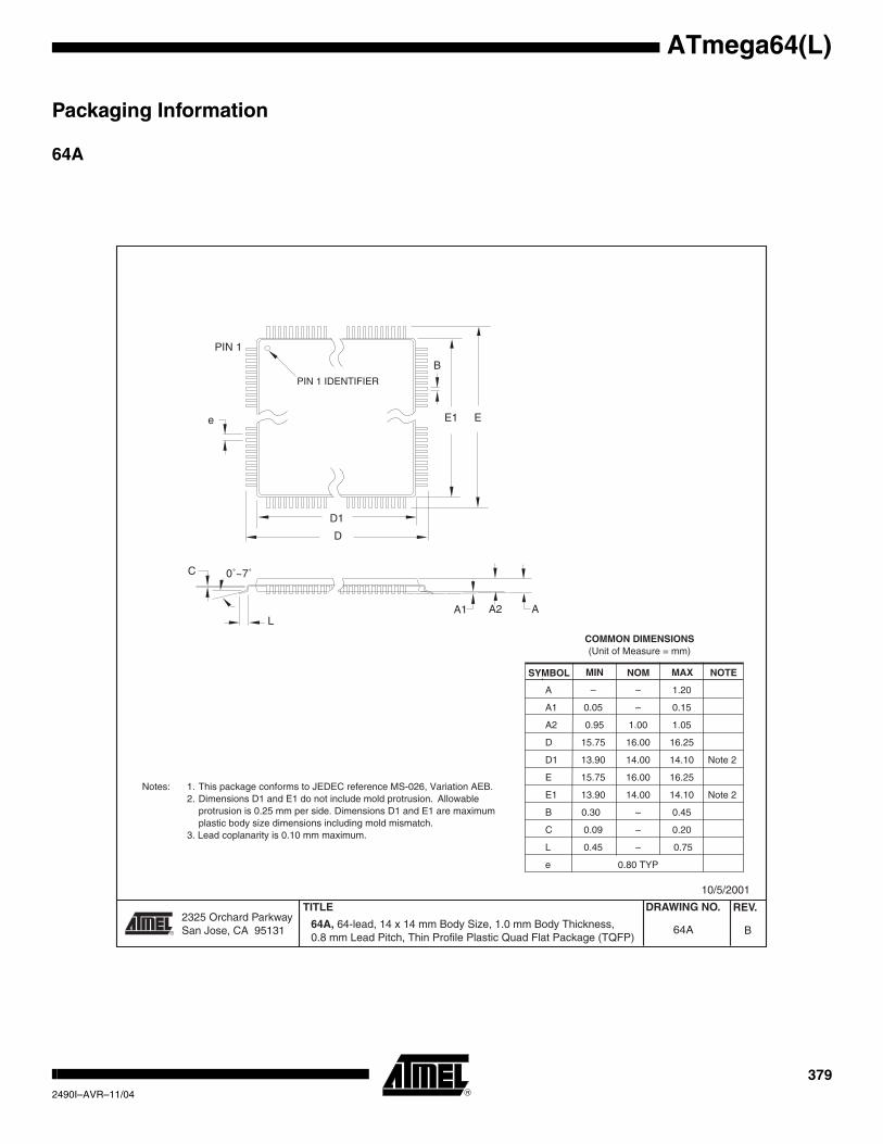
ATmega64(L)
Packaging Information
64A
2325 Orchard Parkway San Jose, CA 95131
TITLE DRAWING NO.
R
REV.
64A, 64-lead, 14 x 14 mm Body Size, 1.0 mm Body Thickness,0.8 mm Lead Pitch, Thin Profile Plastic Quad Flat Package (TQFP)
B64A
10/5/2001
PIN 1 IDENTIFIER
0˚~7˚
PIN 1
L
C
A1 A2 A
D1
D
e E1 E
B
COMMON DIMENSIONS(Unit of Measure = mm)
SYMBOL MIN NOM MAX NOTE
Notes: 1. This package conforms to JEDEC reference MS-026, Variation AEB. 2. Dimensions D1 and E1 do not include mold protrusion. Allowable
protrusion is 0.25 mm per side. Dimensions D1 and E1 are maximum plastic body size dimensions including mold mismatch.
3. Lead coplanarity is 0.10 mm maximum.
A – – 1.20
A1 0.05 – 0.15
A2 0.95 1.00 1.05
D 15.75 16.00 16.25
D1 13.90 14.00 14.10 Note 2
E 15.75 16.00 16.25
E1 13.90 14.00 14.10 Note 2
B 0.30 – 0.45
C 0.09 – 0.20
L 0.45 – 0.75
e 0.80 TYP
3792490I–AVR–11/04
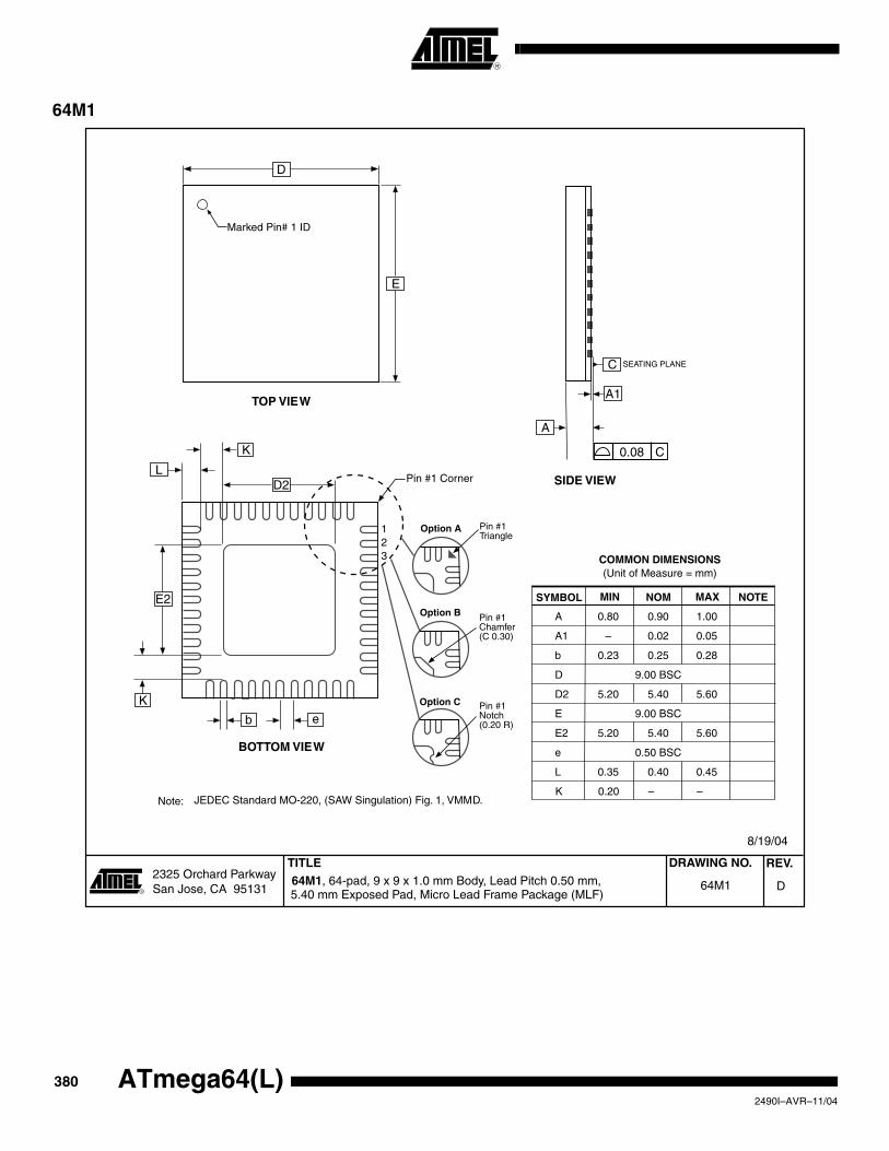
64M1
2325 Orchard Parkway San Jose, CA 95131
TITLE DRAWING NO.
R
REV. 64M1, 64-pad, 9 x 9 x 1.0 mm Body, Lead Pitch 0.50 mm,
D64M1
8/19/04
COMMON DIMENSIONS(Unit of Measure = mm)
SYMBOL MIN NOM MAX NOTE
A 0.80 0.90 1.00
A1 – 0.02 0.05
b 0.23 0.25 0.28
D 9.00 BSC
D2 5.20 5.40 5.60
E 9.00 BSC
E2 5.20 5.40 5.60
e 0.50 BSC
L 0.35 0.40 0.45
Note: JEDEC Standard MO-220, (SAW Singulation) Fig. 1, VMMD.
TOP VIEW
SIDE VIEW
BOTTOM VIEW
D
E
Marked Pin# 1 ID
SEATING PLANE
A1
C
A
C0.08
123
K 0.20 – –
E2
D2
b e
Pin #1 CornerL
Pin #1 Triangle
Pin #1 Chamfer(C 0.30)
Option A
Option B
Pin #1 Notch(0.20 R)
Option C
K
K
5.40 mm Exposed Pad, Micro Lead Frame Package (MLF)
380 ATmega64(L)2490I–AVR–11/04
ATmega64(L)
Errata The revision letter in this section refers to the revision of the ATmega64 device.
ATmega64, all rev. • Stabilizing time needed when changing XDIV Register• Stabilizing time needed when changing OSCCAL Register
1. Stabilizing time needed when changing XDIV Register
After increasing the source clock frequency more than 2% with settings in the XDIVregister, the device may execute some of the subsequent instructions incorrectly.
Problem Fix / Workaround
The NOP instruction will always be executed correctly also right after a frequencychange. Thus, the next 8 instructions after the change should be NOP instructions.To ensure this, follow this procedure:
1.Clear the I bit in the SREG Register.
2.Set the new pre-scaling factor in XDIV register.
3.Execute 8 NOP instructions
4.Set the I bit in SREG
This will ensure that all subsequent instructions will execute correctly.
Assembly Code Example:CLI ; clear global interrupt enable
OUT XDIV, temp ; set new prescale value
NOP ; no operation
NOP ; no operation
NOP ; no operation
NOP ; no operation
NOP ; no operation
NOP ; no operation
NOP ; no operation
NOP ; no operation
SEI ; clear global interrupt enable
2. Stabilizing time needed when changing OSCCAL Register
After increasing the source clock frequency more than 2% with settings in the OSC-CAL register, the device may execute some of the subsequent instructionsincorrectly.
Problem Fix / Workaround
The behavior follows errata number 1., and the same Fix / Workaround is applicableon this errata.
A proposal for solving problems regarding the JTAG instruction IDCODE is presentedbelow.
IDCODE masks data from TDI input
The public but optional JTAG instruction IDCODE is not implemented correctlyaccording to IEEE1149.1; a logic one is scanned into the shift register instead of theTDI input while shifting the Device ID Register. Hence, captured data from the pre-ceding devices in the boundary scan chain are lost and replaced by all-ones, anddata to succeeding devices are replaced by all-ones during Update-DR.
If ATmega64 is the only device in the scan chain, the problem is not visible.
3812490I–AVR–11/04
Problem Fix / Workaround
Select the Device ID Register of the ATmega64 (Either by issuing the IDCODEinstruction or by entering the Test-Logic-Reset state of the TAP controller) to readout the contents of its Device ID Register and possibly data from succeedingdevices of the scan chain. Note that data to succeeding devices cannot be enteredduring this scan, but data to preceding devices can. Issue the BYPASS instructionto the ATmega64 to select its Bypass Register while reading the Device ID Regis-ters of preceding devices of the boundary scan chain. Never read data fromsucceeding devices in the boundary scan chain or upload data to the succeedingdevices while the Device ID Register is selected for the ATmega64. Note that theIDCODE instruction is the default instruction selected by the Test-Logic-Reset stateof the TAP-controller.
Alternative Problem Fix / Workaround
If the Device IDs of all devices in the boundary scan chain must be captured simul-taneously (for instance if blind interrogation is used), the boundary scan chain canbe connected in such way that the ATmega64 is the fist device in the chain. Update-DR will still not work for the succeeding devices in the boundary scan chain as longas IDCODE is present in the JTAG Instruction Register, but the Device ID registeredcannot be uploaded in any case.
382 ATmega64(L)2490I–AVR–11/04
ATmega64(L)
Datasheet Revision History
Please note that the referring page numbers in this section are referred to this docu-ment. The referring revision in this section are referring to the document revision.
Changes from Rev. 2490H-10/04 to Rev. 2490I-11/04
1. Removed “Preliminary” and TBD’s.
2. Updated Table 8 on page 38, Table 11 on page 40, Table 19 on page 51, Table132 on page 329, Table 134 on page 332.
3. Updated features in “Analog to Digital Converter” on page 231.
4. Updated “Electrical Characteristics” on page 327.
Changes from Rev. 2490G-03/04 to Rev. 2490H-10/04
1. Removed references to Analog Ground, IC1/IC3 changed to ICP1/ICP3, InputCapture Trigger changed to Input Capture Pin.
2. Updated “ATmega103 and ATmega64 Compatibility” on page 4.
3. Updated “External Memory Interface” on page 25
4. Updated “XTAL Divide Control Register – XDIV” to “Clock Sources” on page36.
5. Updated code example in “Watchdog Timer Control Register – WDTCR” onpage 56.
6. Added section “Unconnected Pins” on page 70.
7. Updated Table 19 on page 51, Table 20 on page 55, Table 95 on page 237, and Table 60 on page 134.
8. Updated Figure 116 on page 240.
9. Updated “Version” on page 256.
10. Updated “DC Characteristics” on page 327.
11. Updated “ATmega64 Typical Characteristics” on page 342.
12. Updated features in“Analog to Digital Converter” on page 231 and Table 136on page 335.
13. Updated “Ordering Information” on page 378.
Changes from Rev. 2490F-12/03 to Rev. 2490G-03/04
1. Updated “Errata” on page 381.
Changes from Rev. 2490E-09/03 to Rev. 2490F-12/03
1. Updated “Calibrated Internal RC Oscillator” on page 41.
3832490I–AVR–11/04
Changes from Rev. 2490D-02/03 to Rev. 2490E-09/03
1. Updated note in “XTAL Divide Control Register – XDIV” on page 37.
2. Updated “JTAG Interface and On-chip Debug System” on page 49.
3. Updated “Test Access Port – TAP” on page 249 regarding JTAGEN.
4. Updated description for the JTD bit on page 259.
5. Added a note regarding JTAGEN fuse to Table 118 on page 293.
6. Updated RPU values in “DC Characteristics” on page 327.
7. Updated “ADC Characteristics” on page 334.
8. Added a proposal for solving problems regarding the JTAG instructionIDCODE in “Errata” on page 381.
Changes from Rev. 2490C-09/02 to Rev. 2490D-02/03
1. Added reference to Table 124 on page 297 from both SPI Serial Programmingand Self Programming to inform about the Flash page size.
2. Added Chip Erase as a first step under “Programming the Flash” on page 324and “Programming the EEPROM” on page 325.
3. Corrected OCn waveforms in Figure 52 on page 125.
4. Various minor Timer1 corrections.
5. Improved the description in “Phase Correct PWM Mode” on page 100 and onpage 153.
6. Various minor TWI corrections.
7. Added note under "Filling the Temporary Buffer (Page Loading)" about writ-ing to the EEPROM during an SPM page load.
8. Removed ADHSM completely.
9. Added note about masking out unused bits when reading the ProgramCounter in “Stack Pointer” on page 12.
10. Added section “EEPROM Write During Power-down Sleep Mode” on page 23.
11. Changed VHYST value to 120 in Table 19 on page 51.
12. Added information about conversion time for Differential mode with AutoTriggering on page 235.
13. Added tWD_FUSE in Table 128 on page 310.
14. Updated “Packaging Information” on page 379.
384 ATmega64(L)2490I–AVR–11/04
ATmega64(L)
Changes from Rev. 2490B-09/02 to Rev. 2490C-09/02
1. Changed the Endurance on the Flash to 10,000 Write/Erase Cycles.
Changes from Rev. 2490A-10/01 to Rev. 2490B-09/02
1. Added 64-pad MLF Package and updated “Ordering Information” on page 378.
2. Added the section “Using all Locations of External Memory Smaller than 64KB” on page 33.
3. Added the section “Default Clock Source” on page 37.
4. Renamed SPMCR to SPMCSR in entire document.
5. Added Some Preliminary Test Limits and Characterization Data
Removed some of the TBD's and corrected data in the following tables and pages:
Table 2 on page 22, Table 7 on page 36, Table 9 on page 39, Table 10 on page 39,Table 12 on page 40, Table 14 on page 41, Table 16 on page 42, Table 19 on page51, Table 20 on page 55, Table 22 on page 57, “DC Characteristics” on page 327,Table 131 on page 329, Table 134 on page 332, Table 136 on page 335, and Table137 - Table 144.
6. Removed Alternative Algortihm for Leaving JTAG Programming Mode.
See “Leaving Programming Mode” on page 323.
7. Improved description on how to do a polarity check of the ADC diff results in“ADC Conversion Result” on page 243.
8. Updated Programming Figures:
Figure 138 on page 295 and Figure 147 on page 308 are updated to also reflect thatAVCC must be connected during Programming mode. Figure 142 on page 304added to illustrate how to program the fuses.
9. Added a note regarding usage of the “PROG_PAGELOAD (0x6)” and“PROG_PAGEREAD (0x7)” instructions on page 315.
10. Updated “Two-wire Serial Interface” on page 197.
More details regarding use of the TWI Power-down operation and using the TWI asmaster with low TWBRR values are added into the data sheet. Added the note atthe end of the “Bit Rate Generator Unit” on page 203. Added the description at theend of “Address Match Unit” on page 204.
11. Updated Description of OSCCAL Calibration Byte.
In the data sheet, it was not explained how to take advantage of the calibrationbytes for 2, 4, and 8 MHz Oscillator selections. This is now added in the followingsections:
Improved description of “Oscillator Calibration Register – OSCCAL(1)” on page 41and “Calibration Byte” on page 294.
12. When using external clock there are some limitations regards to change offrequency. This is descried in “External Clock” on page 42 and Table 131 onpage 329.
3852490I–AVR–11/04
13. Added a sub section regarding OCD-system and power consumption in thesection “Minimizing Power Consumption” on page 48.
14. Corrected typo (WGM-bit setting) for:
– “Fast PWM Mode” on page 98 (Timer/Counter0).
– “Phase Correct PWM Mode” on page 100 (Timer/Counter0).
– “Fast PWM Mode” on page 151 (Timer/Counter2).
– “Phase Correct PWM Mode” on page 153 (Timer/Counter2).
15. Corrected Table 81 on page 191 (USART).
16. Corrected Table 102 on page 263 (Boundary-Scan)
386 ATmega64(L)2490I–AVR–11/04
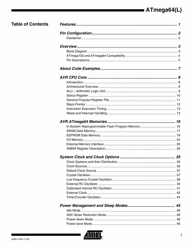
ATmega64(L)
Table of Contents Features................................................................................................ 1
Pin Configuration................................................................................. 2Disclaimer ............................................................................................................. 2
Overview............................................................................................... 3Block Diagram ...................................................................................................... 3ATmega103 and ATmega64 Compatibility ........................................................... 4Pin Descriptions.................................................................................................... 5
About Code Examples......................................................................... 7
AVR CPU Core ..................................................................................... 8Introduction........................................................................................................... 8Architectural Overview.......................................................................................... 8ALU – Arithmetic Logic Unit.................................................................................. 9Status Register ................................................................................................... 10General Purpose Register File ........................................................................... 11Stack Pointer ...................................................................................................... 12Instruction Execution Timing............................................................................... 13Reset and Interrupt Handling.............................................................................. 13
AVR ATmega64 Memories ................................................................ 16In-System Reprogrammable Flash Program Memory ........................................ 16SRAM Data Memory........................................................................................... 17EEPROM Data Memory...................................................................................... 19I/O Memory......................................................................................................... 24External Memory Interface.................................................................................. 25XMEM Register Description................................................................................ 30
System Clock and Clock Options .................................................... 35Clock Systems and their Distribution .................................................................. 35Clock Sources..................................................................................................... 36Default Clock Source .......................................................................................... 37Crystal Oscillator................................................................................................. 37Low-frequency Crystal Oscillator ........................................................................ 39External RC Oscillator ........................................................................................ 40Calibrated Internal RC Oscillator ........................................................................ 41External Clock..................................................................................................... 42Timer/Counter Oscillator..................................................................................... 44
Power Management and Sleep Modes............................................. 45Idle Mode............................................................................................................ 46ADC Noise Reduction Mode............................................................................... 46Power-down Mode.............................................................................................. 46Power-save Mode............................................................................................... 46
i2490I–AVR–11/04
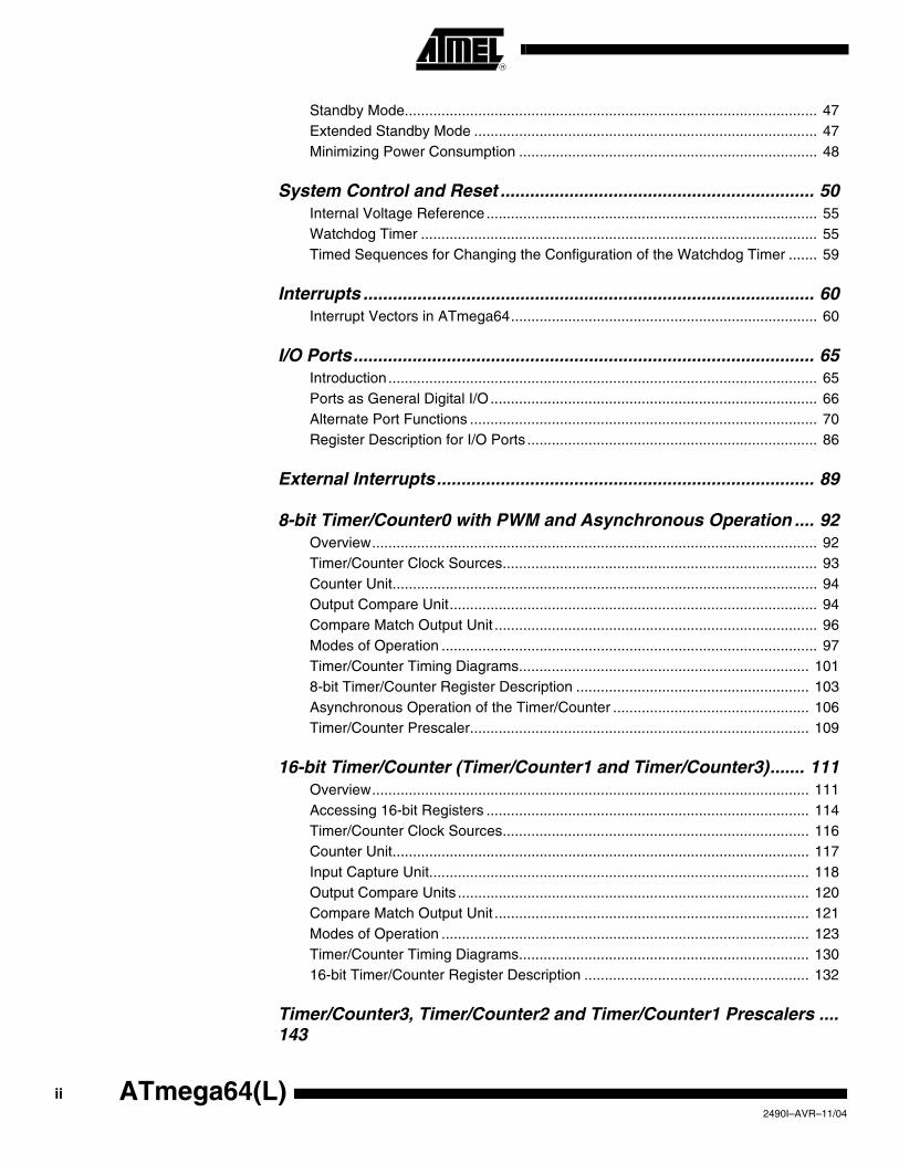
Standby Mode..................................................................................................... 47Extended Standby Mode .................................................................................... 47Minimizing Power Consumption ......................................................................... 48
System Control and Reset ................................................................ 50Internal Voltage Reference................................................................................. 55Watchdog Timer ................................................................................................. 55Timed Sequences for Changing the Configuration of the Watchdog Timer ....... 59
Interrupts ............................................................................................ 60Interrupt Vectors in ATmega64........................................................................... 60
I/O Ports.............................................................................................. 65Introduction......................................................................................................... 65Ports as General Digital I/O................................................................................ 66Alternate Port Functions ..................................................................................... 70Register Description for I/O Ports ....................................................................... 86
External Interrupts............................................................................. 89
8-bit Timer/Counter0 with PWM and Asynchronous Operation .... 92Overview............................................................................................................. 92Timer/Counter Clock Sources............................................................................. 93Counter Unit........................................................................................................ 94Output Compare Unit.......................................................................................... 94Compare Match Output Unit ............................................................................... 96Modes of Operation ............................................................................................ 97Timer/Counter Timing Diagrams....................................................................... 1018-bit Timer/Counter Register Description ......................................................... 103Asynchronous Operation of the Timer/Counter ................................................ 106Timer/Counter Prescaler................................................................................... 109
16-bit Timer/Counter (Timer/Counter1 and Timer/Counter3)....... 111Overview........................................................................................................... 111Accessing 16-bit Registers ............................................................................... 114Timer/Counter Clock Sources........................................................................... 116Counter Unit...................................................................................................... 117Input Capture Unit............................................................................................. 118Output Compare Units ...................................................................................... 120Compare Match Output Unit ............................................................................. 121Modes of Operation .......................................................................................... 123Timer/Counter Timing Diagrams....................................................................... 13016-bit Timer/Counter Register Description ....................................................... 132
Timer/Counter3, Timer/Counter2 and Timer/Counter1 Prescalers .... 143
ii ATmega64(L)2490I–AVR–11/04
ATmega64(L)
8-bit Timer/Counter2 with PWM...................................................... 145Overview........................................................................................................... 145Timer/Counter Clock Sources........................................................................... 146Counter Unit...................................................................................................... 147Output Compare Unit........................................................................................ 147Compare Match Output Unit ............................................................................. 149Modes of Operation .......................................................................................... 150Timer/Counter Timing Diagrams....................................................................... 1548-bit Timer/Counter Register Description ......................................................... 156
Output Compare Modulator (OCM1C2).......................................... 160Overview........................................................................................................... 160Description........................................................................................................ 160
Serial Peripheral Interface – SPI..................................................... 162SS Pin Functionality.......................................................................................... 166Data Modes ...................................................................................................... 169
USART .............................................................................................. 170Overview........................................................................................................... 170Clock Generation .............................................................................................. 171Frame Formats ................................................................................................. 174USART Initialization.......................................................................................... 175Data Transmission – The USART Transmitter ................................................. 176Data Reception – The USART Receiver .......................................................... 180Asynchronous Data Reception ......................................................................... 183Multi-processor Communication Mode ............................................................. 186USART Register Description ............................................................................ 187Examples of Baud Rate Setting........................................................................ 192
Two-wire Serial Interface ................................................................ 197Features............................................................................................................ 197Two-wire Serial Interface Bus Definition........................................................... 197Data Transfer and Frame Format ..................................................................... 198Multi-master Bus Systems, Arbitration and Synchronization ............................ 201Overview of the TWI Module ............................................................................ 203TWI Register Description.................................................................................. 206Using the TWI................................................................................................... 209Transmission Modes......................................................................................... 213Multi-master Systems and Arbitration............................................................... 226
Analog Comparator ......................................................................... 228Analog Comparator Multiplexed Input .............................................................. 230
Analog to Digital Converter ............................................................ 231Features............................................................................................................ 231
iii2490I–AVR–11/04
Operation.......................................................................................................... 232Starting a Conversion ....................................................................................... 233Prescaling and Conversion Timing................................................................... 234Changing Channel or Reference Selection ...................................................... 237ADC Noise Canceler......................................................................................... 239ADC Conversion Result.................................................................................... 243
JTAG Interface and On-chip Debug System ................................. 249Features............................................................................................................ 249Overview........................................................................................................... 249Test Access Port – TAP.................................................................................... 249TAP Controller .................................................................................................. 251Using the Boundary -scan Chain ...................................................................... 252Using the On-chip Debug system..................................................................... 252On-chip Debug Specific JTAG Instructions ...................................................... 253On-chip Debug Related Register in I/O Memory .............................................. 254Using the JTAG Programming Capabilities ...................................................... 254Bibliography ...................................................................................................... 254
IEEE 1149.1 (JTAG) Boundary-scan .............................................. 255Features............................................................................................................ 255System Overview.............................................................................................. 255Data Registers .................................................................................................. 255Boundary-scan Specific JTAG Instructions ...................................................... 257Boundary-scan Related Register in I/O Memory .............................................. 259Boundary-scan Chain ....................................................................................... 259ATmega64 Boundary-scan Order..................................................................... 271Boundary-scan Description Language Files ..................................................... 277
Boot Loader Support – Read-While-Write Self-programming ..... 278Features............................................................................................................ 278Application and Boot Loader Flash Sections .................................................... 278Read-While-Write and No Read-While-Write Flash Sections........................... 278Boot Loader Lock Bits....................................................................................... 280Entering the Boot Loader Program................................................................... 282Addressing the Flash During Self-programming............................................... 284Self-programming the Flash ............................................................................. 285
Memory Programming..................................................................... 291Program and Data Memory Lock Bits............................................................... 291Fuse Bits........................................................................................................... 292Signature Bytes ................................................................................................ 294Calibration Byte ................................................................................................ 294Parallel Programming Parameters, Pin Mapping, and Commands .................. 294Parallel Programming ....................................................................................... 298Serial Downloading........................................................................................... 307
iv ATmega64(L)2490I–AVR–11/04
ATmega64(L)
SPI Serial Programming Pin Mapping .............................................................. 308Programming Via the JTAG Interface............................................................... 313
Electrical Characteristics................................................................ 327Absolute Maximum Ratings*............................................................................. 327DC Characteristics............................................................................................ 327External Clock Drive Waveforms...................................................................... 329External Clock Drive ......................................................................................... 329Two-wire Serial Interface Characteristics ......................................................... 330SPI Timing Characteristics ............................................................................... 332ADC Characteristics ......................................................................................... 334External Data Memory Timing .......................................................................... 337
ATmega64 Typical Characteristics ................................................ 342
Register Summary ........................................................................... 372
Instruction Set Summary ................................................................ 375
Ordering Information....................................................................... 378
Packaging Information .................................................................... 37964A ................................................................................................................... 37964M1................................................................................................................. 380
Errata ................................................................................................ 381ATmega64, all rev............................................................................................. 381
Datasheet Revision History ............................................................ 383Changes from Rev. 2490H-10/04 to Rev. 2490I-11/04 .................................... 383Changes from Rev. 2490G-03/04 to Rev. 2490H-10/04................................... 383Changes from Rev. 2490F-12/03 to Rev. 2490G-03/04................................... 383Changes from Rev. 2490E-09/03 to Rev. 2490F-12/03 ................................... 383Changes from Rev. 2490D-02/03 to Rev. 2490E-09/03................................... 384Changes from Rev. 2490C-09/02 to Rev. 2490D-02/03................................... 384Changes from Rev. 2490B-09/02 to Rev. 2490C-09/02................................... 385Changes from Rev. 2490A-10/01 to Rev. 2490B-09/02 ................................... 385
Table of Contents ................................................................................. i
v2490I–AVR–11/04

vi ATmega64(L)2490I–AVR–11/04
Printed on recycled paper.
2490I–AVR–11/04
Disclaimer: The information in this document is provided in connection with Atmel products. No license, express or implied, by estoppel or otherwise, to anyintellectual property right is granted by this document or in connection with the sale of Atmel products. EXCEPT AS SET FORTH IN ATMEL’S TERMS AND CONDI-TIONS OF SALE LOCATED ON ATMEL’S WEB SITE, ATMEL ASSUMES NO LIABILITY WHATSOEVER AND DISCLAIMS ANY EXPRESS, IMPLIED OR STATUTORYWARRANTY RELATING TO ITS PRODUCTS INCLUDING, BUT NOT LIMITED TO, THE IMPLIED WARRANTY OF MERCHANTABILITY, FITNESS FOR A PARTICULARPURPOSE, OR NON-INFRINGEMENT. IN NO EVENT SHALL ATMEL BE LIABLE FOR ANY DIRECT, INDIRECT, CONSEQUENTIAL, PUNITIVE, SPECIAL OR INCIDEN-TAL DAMAGES (INCLUDING, WITHOUT LIMITATION, DAMAGES FOR LOSS OF PROFITS, BUSINESS INTERRUPTION, OR LOSS OF INFORMATION) ARISING OUTOF THE USE OR INABILITY TO USE THIS DOCUMENT, EVEN IF ATMEL HAS BEEN ADVISED OF THE POSSIBILITY OF SUCH DAMAGES. Atmel makes norepresentations or warranties with respect to the accuracy or completeness of the contents of this document and reserves the right to make changes to specificationsand product descriptions at any time without notice. Atmel does not make any commitment to update the information contained herein. Atmel’s products are notintended, authorized, or warranted for use as components in applications intended to support or sustain life.
Atmel Corporation Atmel Operations
2325 Orchard ParkwaySan Jose, CA 95131, USATel: 1(408) 441-0311Fax: 1(408) 487-2600
Regional Headquarters
EuropeAtmel SarlRoute des Arsenaux 41Case Postale 80CH-1705 FribourgSwitzerlandTel: (41) 26-426-5555Fax: (41) 26-426-5500
AsiaRoom 1219Chinachem Golden Plaza77 Mody Road TsimshatsuiEast KowloonHong KongTel: (852) 2721-9778Fax: (852) 2722-1369
Japan9F, Tonetsu Shinkawa Bldg.1-24-8 ShinkawaChuo-ku, Tokyo 104-0033JapanTel: (81) 3-3523-3551Fax: (81) 3-3523-7581
Memory2325 Orchard ParkwaySan Jose, CA 95131, USATel: 1(408) 441-0311Fax: 1(408) 436-4314
Microcontrollers2325 Orchard ParkwaySan Jose, CA 95131, USATel: 1(408) 441-0311Fax: 1(408) 436-4314
La ChantrerieBP 7060244306 Nantes Cedex 3, FranceTel: (33) 2-40-18-18-18Fax: (33) 2-40-18-19-60
ASIC/ASSP/Smart CardsZone Industrielle13106 Rousset Cedex, FranceTel: (33) 4-42-53-60-00Fax: (33) 4-42-53-60-01
1150 East Cheyenne Mtn. Blvd.Colorado Springs, CO 80906, USATel: 1(719) 576-3300Fax: 1(719) 540-1759
Scottish Enterprise Technology ParkMaxwell BuildingEast Kilbride G75 0QR, Scotland Tel: (44) 1355-803-000Fax: (44) 1355-242-743
RF/AutomotiveTheresienstrasse 2Postfach 353574025 Heilbronn, GermanyTel: (49) 71-31-67-0Fax: (49) 71-31-67-2340
1150 East Cheyenne Mtn. Blvd.Colorado Springs, CO 80906, USATel: 1(719) 576-3300Fax: 1(719) 540-1759
Biometrics/Imaging/Hi-Rel MPU/High Speed Converters/RF Datacom
Avenue de RochepleineBP 12338521 Saint-Egreve Cedex, FranceTel: (33) 4-76-58-30-00Fax: (33) 4-76-58-34-80
Literature Requestswww.atmel.com/literature
© Atmel Corporation 2004. All rights reserved. Atmel®, logo and combinations thereof, AVR®, and AVR Studio® are registered trademarks,and Everywhere You Are™ are the trademarks of Atmel Corporation or its subsidiaries. Microsoft®, Windows®, Windows NT®, and Windows XP®
are the registered trademarks of Microsoft Corporation.Other terms and product names may be trademarks of others.


![Atmel 8-bit AVR Microcontroller with 2/4/8K Bytes In ...files.microjpm.webnode.com/200001398-94b6996aae... · ATtiny25/45/85 [DATASHEET] 2 2586Q–AVR–08/2013 1. Pin Configurations](https://img.dokumen.tips/doc/110x75/5aef7d037f8b9ad0618cdefe/atmel-8-bit-avr-microcontroller-with-248k-bytes-in-files-datasheet-2-2586qavr082013.jpg)