Embed Size (px)
Citation preview

8 Bit ALUKatie Leis, Jon Stanley, Julian Kemmerer
Specifications OverviewAn overview on our project - introduction, specifications, objective.
● Inputs○ ALU Op Code (3 bits)○ Data0 (8 bits)○ Data1 (8 bits)
● Outputs○ Result (8 bits)○ Zero flag (sent to control for jump logic)
● 8 Operations:○ Logic (AND, OR, NOT)○ Arithmetic (ADD, SUB)○ Shifts (left, right arithmetic, right logical)

Block DiagramA breakdown of the various blocks.
ADD
SUB
AND
OR
NOT
SRA
SRL
SL
OUT
OUT == 0 ZERO
ALU_OP[0:2]
x8
x8
x8
x8
x8
x8
x8
x8
x8
x8
x8
x8 x8
x8
x8
x8
x8
x8
x8
x8
x8
0
1
2
3
4
5
6
7

ADD BlockA breakdown of the various blocks, continued.

SUB BlockA breakdown of the various blocks, continued.

AND BlockA breakdown of the various blocks, continued.

OR BlockA breakdown of the various blocks, continued.

NOT BlockA breakdown of the various blocks, continued.

SRA BlockA breakdown of the various blocks, continued.
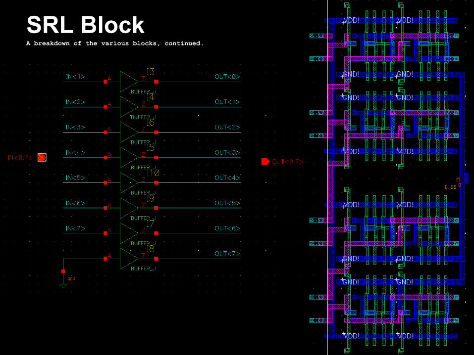
SRL BlockA breakdown of the various blocks, continued.

SL BlockA breakdown of the various blocks, continued.

Zero Flag BlockA breakdown of the various blocks, continued.

Eight 8-Bit to One 8-Bit Mux BlockA breakdown of the various blocks, continued.

Top Level Block SchematicA breakdown of the various blocks, continued.

Top Level Block LayoutA breakdown of the various blocks, continued.

Speed / Power / Area SummaryPower and timing characteristics of the circuit blocks.
● Area:○ 145 um x 230 um○ 33,350 (um squared)○ 0.03335 (mm squared)
● Power:○ Maximum current draw*: ~236 mA
● Timing:○ Input -> Zero Flag○ Maximum delay*: 456.7 ps○ ~2.19 GHz
*1) Simulations did not use extracted cell views. Values obtained are from schematic models only. 2) Simulations did not explore the full space of possible input patterns. The measured maximum values do not necessarily reflect absolute circuit maximums.

Design ConstraintsAny design constraints we experienced.
● Some routing was tricky due to small size of standard cells and number of inputs that needed to be connected
● Time was a big factor in the overall design● PDK is hard to work with

Pre-layout SimulationSimulations that prove the functionality of the circuit blocks.
Data0 - Data1 Data0 + Data1

Post-layout SimulationSimulations that prove the functionality of the circuit blocks.
● Extraction not working at current time.● Circuits are LVS/DRC clean.● Schematic simulation results assumed to be
reasonable approximation.

DRC/LVSDRC and LVS of our final layout.

QUESTIONS?

Progress Summary
Task Symbol Schematic Simulation Layout
ALU TOP 100% 100% 100% 100%
ADD Block 100% 100% 100% 100%
SUB Block 100% 100% 100% 100%
AND Block 100% 100% 100% 100%
OR Block 100% 100% 100% 100%
NOT Block 100% 100% 100% 100%
SRA Block 100% 100% 100% 100%
SRL Block 100% 100% 100% 100%
SL Block 100% 100% 100% 100%
Zero-Flag Block 100% 100% 100% 100%
Eight 8-Bit to One 8-Bit Mux 100% 100% 100% 100%