Embed Size (px)
Citation preview

USB58077-Port USB 3.1 Gen 1 Hub
Highlights• USB Hub with 7 USB 3.1 Gen 1 / USB 2.0 down-
stream ports• USB-IF Battery Charger revision 1.2 support on
up & downstream ports (DCP, CDP, SDP)
• FlexConnect: Downstream port able to swap with upstream port, allowing master capable devices to control other devices on the hub
• USB Link Power Management (LPM) support
• Enhanced OEM configuration options available through either OTP or SPI ROM
• Available in 100-pin (12mm x 12mm) VQFN RoHS compliant package
• Commercial and industrial grade temperature support
Target Applications• Standalone USB Hubs• Laptop Docks• PC Motherboards• PC Monitor Docks• Multi-function USB 3.1 Gen 1 Peripherals
Key Benefits
• USB 3.1 Gen 1 compliant 5 Gbps, 480 Mbps, 12 Mbps, and 1.5Mbps operation- 5V tolerant USB 2.0 pins- 1.32V tolerant USB 3.1 Gen 1 pins- Integrated termination and pull-up/down resistors
• Supports battery charging of most popular battery powered devices on all ports- USB-IF Battery Charging rev. 1.2 support
(DCP, CDP, SDP)- Apple® portable product charger emulation- Chinese YD/T 1591-2006 charger emulation- Chinese YD/T 1591-2009 charger emulation- European Union universal mobile charger support- Support for Microchip UCS100x family of battery
charging controllers- Supports additional portable devices
• Smart port controller operation- Firmware handling of companion port power
controllers
• On-chip microcontroller- manages I/Os, VBUS, and other signals
• 8 KB RAM, 64 KB ROM
• 8 KB One-Time-Programmable (OTP) ROM- Includes on-chip charge pump
• Configuration programming via OTP ROM, SPI ROM, or SMBus
• FlexConnect- Reversible upstream and downstream Port 1 roles
on command
• PortSwap- Configurable USB 2.0 differential pair signal swap
• PHYBoostTM
- Programmable USB transceiver drive strength for recovering signal integrity
• VariSenseTM
- Programmable USB receive sensitivity
• Port Split- USB2.0 and USB3.1 Gen1 port operation can be
split for custom applications using embedded USB3.x devices in parallel with USB2.0 devices.
• Compatible with Microsoft Windows 10, 8, 7, XP, Apple OS X 10.4+, and Linux hub drivers
• Optimized for low-power operation and low ther-mal dissipation
• Package- 100-pin VQFN (12mm x 12mm)
2016-2017 Microchip Technology Inc. DS00002237C-page 1

USB5807
TO OUR VALUED CUSTOMERS
It is our intention to provide our valued customers with the best documentation possible to ensure successful use of your Microchipproducts. To this end, we will continue to improve our publications to better suit your needs. Our publications will be refined andenhanced as new volumes and updates are introduced.
If you have any questions or comments regarding this publication, please contact the Marketing Communications Department viaE-mail at [email protected] or fax the Reader Response Form in the back of this data sheet to (480) 792-4150. Wewelcome your feedback.
Most Current Data Sheet
To obtain the most up-to-date version of this data sheet, please register at our Worldwide Web site at:
http://www.microchip.com
You can determine the version of a data sheet by examining its literature number found on the bottom outside corner of any page.The last character of the literature number is the version number, (e.g., DS30000A is version A of document DS30000).
Errata
An errata sheet, describing minor operational differences from the data sheet and recommended workarounds, may exist for currentdevices. As device/documentation issues become known to us, we will publish an errata sheet. The errata will specify the revisionof silicon and revision of document to which it applies.
To determine if an errata sheet exists for a particular device, please check with one of the following:
• Microchip’s Worldwide Web site; http://www.microchip.com• Your local Microchip sales office (see last page)When contacting a sales office, please specify which device, revision of silicon and data sheet (include literature number) you areusing.
Customer Notification System
Register on our web site at www.microchip.com to receive the most current information on all of our products.
DS00002237C-page 2 2016-2017 Microchip Technology Inc.

2016-2017 Microchip Technology Inc. DS00002237C-page 3
USB5807
TABLE OF CONTENTS
Introduction ........................................................................................................................................................................................... 7Pin Descriptions and Configuration ....................................................................................................................................................... 6Functional Descriptions ......................................................................................................................................................................... 9Operational Characteristics................................................................................................................................................................. 13System Application ............................................................................................................................................................................. 19Package Outlines ................................................................................................................................................................................ 26Revision History ................................................................................................................................................................................... 29The Microchip Web Site ...................................................................................................................................................................... 30Customer Change Notification Service ............................................................................................................................................... 30Customer Support ............................................................................................................................................................................... 30Product Identification System ............................................................................................................................................................. 31

USB5807
1.0 PREFACE
1.1 General Terms
TABLE 1-1: GENERAL TERMS
Term Description
ADC Analog-to-Digital Converter
Byte 8 bits
CDC Communication Device Class
CSR Control and Status Registers
DWORD 32 bits
EOP End of Packet
EP Endpoint
FIFO First In First Out buffer
FS Full-Speed
FSM Finite State Machine
GPIO General Purpose I/O
HS Hi-Speed
HSOS High Speed Over Sampling
Hub Feature Controller The Hub Feature Controller, sometimes called a Hub Controller for short is the internal processor used to enable the unique features of the USB Controller Hub. This is not to be confused with the USB Hub Controller that is used to communicate the hub status back to the Host during a USB session.
I2C Inter-Integrated Circuit
LS Low-Speed
lsb Least Significant Bit
LSB Least Significant Byte
msb Most Significant Bit
MSB Most Significant Byte
N/A Not Applicable
NC No Connect
OTP One Time Programmable
PCB Printed Circuit Board
PCS Physical Coding Sublayer
PHY Physical Layer
PLL Phase Lock Loop
RESERVED Refers to a reserved bit field or address. Unless otherwise noted, reserved bits must always be zero for write operations. Unless otherwise noted, values are not guaran-teed when reading reserved bits. Unless otherwise noted, do not read or write to reserved addresses.
SDK Software Development Kit
SMBus System Management Bus
UUID Universally Unique IDentifier
WORD 16 bits
DS00002237C-page 4 2016-2017 Microchip Technology Inc.

USB5807
1.2 Reference Documents
1. UNICODE UTF-16LE For String Descriptors USB Engineering Change Notice, December 29th, 2004, http://www.usb.org
2. Universal Serial Bus Revision 3.1 Specification, http://www.usb.org
3. Battery Charging Specification, Revision 1.2, Dec. 07, 2010, http://www.usb.org
4. I2C-Bus Specification, Version 1.1, http://www.nxp.com
5. System Management Bus Specification, Version 1.0, http://smbus.org/specs
2016-2017 Microchip Technology Inc. DS00002237C-page 5

USB5807
2.0 INTRODUCTION
2.1 General Description
The Microchip USB5807 hub is a low-power, OEM configurable, USB 3.1 Gen 1 hub controller with 7 downstream portsand advanced features for embedded USB applications. The USB5807 is fully compliant with the Universal Serial BusRevision 3.1 Specification and USB 2.0 Link Power Management Addendum. The USB5807 supports 5 Gbps Super-Speed (SS), 480 Mbps Hi-Speed (HS), 12 Mbps Full-Speed (FS), and 1.5 Mbps Low-Speed (LS) USB downstreamdevices on all enabled downstream ports.
The USB5807 supports the legacy USB speeds (HS/FS/LS) through a dedicated USB 2.0 hub controller that is the cul-mination of five generations of Microchip hub controller design and experience with proven reliability, interoperability,and device compatibility. The SuperSpeed hub controller operates in parallel with the USB 2.0 hub controller, decouplingthe 5 Gbps SS data transfers from bottlenecks due to the slower USB 2.0 traffic.
The USB5807 enables OEMs to configure their system using “Configuration Straps.” These straps simplify the config-uration process, assigning default values to USB 3.1 Gen 1 ports and GPIOs. OEMs can disable ports, enable batterycharging, and define GPIO functions as default assignments on power-up, removing the need for OTP or external SPIROM.
The USB5807 supports downstream battery charging via the integrated battery charger detection circuitry, which sup-ports the USB-IF Battery Charging (BC1.2) detection method and most Apple devices. The USB5807 provides the bat-tery charging handshake and supports the following USB-IF BC1.2 charging profiles:
• DCP: Dedicated Charging Port (Power brick with no data)
• CDP: Charging Downstream Port (1.5A with data)
• SDP: Standard Downstream Port (0.5A with data)
• Custom profiles loaded via SMBus or OTP
Additionally, the USB5807 includes many powerful and unique features such as:
FlexConnect, which provides flexible connectivity options. One of the USB5807’s downstream ports can be reconfig-ured to become the upstream port, allowing master capable devices to control other devices on the hub.
PortSwap, which adds per-port programmability to USB differential-pair pin locations. PortSwap allows direct alignmentof USB signals (D+/D-) to connectors to avoid uneven trace length or crossing of the USB differential signals on thePCB.
PHYBoost, which provides programmable levels of Hi-Speed USB signal drive strengthin the downstream port transceivers. PHYBoost attempts to restore USB signal integrityin a compromised system environment. The graphic on the right shows an example ofHi-Speed USB eye diagrams before and after PHYBoost signal integrity restoration. ina compromised system environment.
VariSense, which controls the USB receiver sensitivity enabling programmable levels of USB signal receive sensitivity.This capability allows operation in a sub-optimal system environment, such as when a captive USB cable is used.
Port Split, which allows for the USB3.1 Gen1 and USB2.0 portions of downstream ports 5 and 6 to operate inde-pendently and enumerate two separate devices in parallel in special applications.
The USB5807 can be configured for operation through internal default settings. Custom OEM configurations are sup-ported through external SPI ROM or OTP ROM. All port control signal pins are under firmware control in order to allowfor maximum operational flexibility, and are available as GPIOs for customer specific use.
The USB5807 is available in commercial (0°C to +70°C) and industrial (-40°C to +85°C) temperature ranges. An internalblock diagram of the USB5807 is shown in Figure 2-1.
DS00002237C-page 6 2016-2017 Microchip Technology Inc.

USB5807
FIGURE 2-1: INTERNAL BLOCK DIAGRAM
Hub Controller Logic
I2C/SMB
I2C from Master
25 Mhz
USB3 USB2
P3‘A’
AFE0
P4‘A’
P5‘A’
P6‘A’
+3.3 V
+1.2 V
P1‘A’
P2‘A’
P0 ‘B’
P7‘A’
AFE5AFE4AFE3AFE2AFE1 AFE3 AFE4 AFE5 AFE6AFE2 AFE6AFE1 AFE7AFE7
AFE0
2016-2017 Microchip Technology Inc. DS00002237C-page 7

USB5807
3.0 PIN DESCRIPTIONS
3.1 Pin Diagram
Note 1: Configuration straps are identified by an underlined symbol name. Signals that function as configurationstraps must be augmented with an external resistor when connected to a load. Refer to Section 3.5, Con-figuration Straps and Programmable Functions
FIGURE 3-1: PIN ASSIGNMENTS (TOP VIEW)
100
99
98
97
96
95
94
93
92
90
89
88
87
86
85
91
16
15
14
13
12
11
1098654321 7
41
40
39
37
36
35
34
33
32
31
30
29
28
27
26
75 74 73 72 71 70 68 67 66 6569 64 63 62 61 60
38
RB
IAS
XT
AL
O
XT
AL
I/C
LK
IN
US
B3D
N_R
XD
M1
US
B3D
N_R
XD
P1
VD
D12
USB
3DN
_TX
DM
1
USB
3DN
_TX
DP
1
USB
2DN
_DM
1/PR
T_D
IS_M
1
US
B2D
N_D
P1/
PR
T_D
IS_P
1
VDD33
USB2DN_DM4/PRT_DIS_M4
USB2DN_DP4/PRT_DIS_P4
USB3DN_TXDM4
USB3DN_TXDP4
USB2DN_DP3/PRT_DIS_P3
USB3DN_RXDM3
USB3DN_RXDP3
USB3DN_TXDM3
USB3DN_TXDP3
USB2DN_DM3/PRT_DIS_M3
VDD12
VDD12
SP
EE
D_I
ND
4/B
C_I
ND
4/G
PIO
3
C_A
TT
AC
H1/
GP
IO1
PR
T_C
TL
1/G
PIO
17
SP
I_C
E_N
/GP
IO7/
CF
G_N
ON
_RE
M
SP
I_D
I/G
PIO
9/C
FG
_BC
_EN
SP
EE
D_I
ND
6/B
C_I
ND
6/G
PIO
66
SPI_
DO
/C_A
TT
AC
H2/
GP
IO5
SM
BC
LK
/GP
IO8
SP
I_C
LK
/C_A
TT
AC
H3/
GP
IO4
GP
IO69
SPE
ED
_IN
D1/
BC
_IN
D1/
GP
IO70
25
24
23
22
21
20
19
18
17
50
49
48
46
45
44
43
42
47
SPEED_IND5/BC_IND5/GPIO65
VDD12
59 58 57 56 55 54 53 52 51P
RT
_CT
L6/
GP
IO22
SPE
ED
_IN
D3/
BC
_IN
D3/
GP
IO2
PR
T_C
TL
2/G
PIO
18
VD
D33
VD
D33
SP
EE
D_I
ND
2/B
C_I
ND
2/G
PIO
71
PR
T_C
TL
3/G
PIO
19
84
83
81
80
79
78
77
76
82
VD
D33
GP
IO12
/CF
G_S
TR
AP
USB3DN_RXDM4
USB3DN_RXDP4
VD
D12
C_ATTACH0/GPIO64
VD
D33
US
B3D
N_R
XD
M2
US
B3D
N_R
XD
P2
VD
D12
USB
3DN
_TX
DM
2
USB
3DN
_TX
DP
2
USB
2DN
_DM
2/PR
T_D
IS_M
2
US
B2D
N_D
P2/
PR
T_D
IS_P
2
FLE
X_C
MD
/GP
IO10
FL
EX
_ST
AT
E/G
PIO
72
TE
STE
N
VB
US
_DE
T/G
PIO
16
RE
SET
_N
SUSP_IND/GPIO68
VDD12
USB3DN_RXDM7
USB3DN_RXDP7
VDD12
USB3DN_TXDM7
USB3DN_TXDP7
USB2DN_DM7/PRT_DIS_M7
USB2DN_DP7/PRT_DIS_P7
USB3DN_RXDM6
USB3DN_RXDP6
VDD12
USB3DN_TXDM6
USB3DN_TXDP6
USB2DN_DM6/PRT_DIS_M6
USB2DN_DP6/PRT_DIS_P6
USB3UP_RXDM
USB3UP_RXDP
VDD12
USB3UP_TXDM
USB3UP_TXDP
USB2UP_DM
USB2UP_DP
VDD33
USB2DN_DM5/PRT_DIS_M5
USB2DN_DP5/PRT_DIS_P5
USB3DN_TXDM5
USB3DN_TXDP5
VDD12
USB3DN_RXDM5
USB3DN_RXDP5
VDD33
PR
T_C
TL
7/G
PIO
23
SPE
ED
_IN
D7/
BC
_IN
D7/
GP
IO67
VD
D33
SM
BD
AT
A/G
PIO
6
PR
T_C
TL
5/G
PIO
21
PRT
_CT
L4/
GA
NG
_PW
R/G
PIO
20
thermal slug connects to VSS
MicrochipUSB5807
(Top View 100-VQFN)
DS00002237C-page 8 2016-2017 Microchip Technology Inc.

USB5807
3.2 Pin Symbols
Pin Num. Pin Name Reset Pin Num. Pin Name Reset
1 RBIAS A/P 51 PRT_CTL6/GPIO22 PD-50k
2 VDD33 A/P 52 PRT_CTL5/GPIO21 PD-50k
3 XTALI/CLKIN A/P 53 PRT_CTL7/GPIO23 PD-50k
4 XTALO A/P 54 VDD33 A/P
5 VDD33 A/P 55 SPEED_IND7/BC_IND7/GPIO67 Z
6 USB2DN_DP1/PRT_DIS_P1 PD-15k 56 SPEED_IND3/BC_IND3/GPIO2 Z
7 USB2DN_DM1/PRT_DIS_M1 PD-15k 57 PRT_CTL4/GANG_PWR/GPIO20 PD-50k
8 USB3DN_TXDP1 Z 58 PRT_CTL3/GPIO19 PD-50k
9 USB3DN_TXDM1 Z 59 VDD12 A/P
10 VDD12 A/P 60 SPEED_IND4/BC_IND4/GPIO3 Z
11 USB3DN_RXDP1 Z 61 SPEED_IND2/BC_IND2/GPIO71 Z
12 USB3DN_RXDM1 Z 62 PRT_CTL2/GPIO18 PD-50k
13 USB2DN_DP2/PRT_DIS_P2 PD-15k 63 SPEED_IND1/BC_IND1/GPIO70 Z
14 USB2DN_DM2/PRT_DIS_M2 PD-15k 64 VDD33 A/P
15 USB3DN_TXDP2 Z 65 SPI_CLK/C_ATTACH3/GPIO4 Z
16 USB3DN_TXDM2 Z 66 SPI_DO/C_ATTACH2/GPIO5 PD-50k
17 VDD12 A/P 67 SPI_DI/GPIO9/CFG_BC_EN Z
18 USB3DN_RXDP2 Z 68 SPI_CE_N/GPIO7/CFG_NON_REM PU-50k
19 USB3DN_RXDM2 Z 69 GPIO69 Z
20 GPIO12/CFG_STRAP Z 70 PRT_CTL1/GPIO17 PD-50k
21 FLEX_CMD/GPIO10 Z 71 SPEED_IND6/BC_IND6/GPIO66 Z
22 FLEX_STATE/GPIO72 Z 72 VDD33 A/P
23 TESTEN Z 73 C_ATTACH1/GPIO1 Z
24 VBUS_DET/GPIO16 Z 74 SMBDATA/GPIO6 Z
25 RESET_N R 75 SMBCLK/GPIO8 Z
26 VDD12 A/P 76 C_ATTACH0/GPIO64 Z
27 VDD33 A/P 77 SUSP_IND/GPIO68 Z
28 USB2DN_DP3/PRT_DIS_P3 PD-15k 78 VDD12 A/P
29 USB2DN_DM3/PRT_DIS_M3 PD-15k 79 USB2DN_DP7/PRT_DIS_P7 PD-15k
30 USB3DN_TXDP3 Z 80 USB2DN_DM7/PRT_DIS_M7 PD-15k
31 USB3DN_TXDM3 Z 81 USB3DN_TXDP7 Z
32 VDD12 A/P 82 USB3DN_TXDM7 Z
33 USB3DN_RXDP3 Z 83 VDD12 A/P
34 USB3DN_RXDM3 Z 84 USB3DN_RXDP7 Z
35 USB2DN_DP4/PRT_DIS_P4 PD-15k 85 USB3DN_RXDM7 Z
36 USB2DN_DM4/PRT_DIS_M4 PD-15k 86 USB2DN_DP6/PRT_DIS_P6 PD-15k
37 USB3DN_TXDP4 Z 87 USB2DN_DM6/PRT_DIS_M6 PD-15k
38 USB3DN_TXDM4 Z 88 USB3DN_TXDP6 Z
39 VDD12 A/P 89 USB3DN_TXDM6 Z
40 USB3DN_RXDP4 Z 90 VDD12 A/P
41 USB3DN_RXDM4 Z 91 USB3DN_RXDP6 Z
42 VDD33 A/P 92 USB3DN_RXDM6 Z
43 USB2DN_DP5/PRT_DIS_P5 PD-15k 93 VDD33 A/P
44 USB2DN_DM5/PRT_DIS_M5 PD-15k 94 USB2UP_DP PD-1M
45 USB3DN_TXDP5 Z 95 USB2UP_DM PD-1M
46 USB3DN_TXDM5 Z 96 USB3UP_TXDP Z
47 VDD12 A/P 97 USB3UP_TXDM Z
48 USB3DN_RXDP5 Z 98 VDD12 A/P
49 USB3DN_RXDM5 Z 99 USB3UP_RXDP Z
50 SPEED_IND5/BC_IND5/GPIO65 Z 100 USB3UP_RXDM Z
2016-2017 Microchip Technology Inc. DS00002237C-page 9

USB5807
The pin reset state definitions are detailed in Table 3-1.
3.3 USB5807 Pin Descriptions
This section contains descriptions of the various USB5807 pins. The pin descriptions have been broken into functionalgroups as follows:
• USB 3.1 Gen 1 Pin Descriptions
• USB 2.0 Pin Descriptions
• Port Control Pin Descriptions
• SPI Interface
• USB Type-C Connector Controls
• Miscellaneous Pin Descriptions
• Configuration Strap Pin Descriptions
• Power and Ground Pin Descriptions
The “_N” symbol in the signal name indicates that the active, or asserted, state occurs when the signal is at a low voltagelevel. For example, RESET_N indicates that the reset signal is active low. When “_N” is not present after the signalname, the signal is asserted when at the high voltage level.
The terms assertion and negation are used exclusively. This is done to avoid confusion when working with a mixture of“active low” and “active high” signal. The term assert, or assertion, indicates that a signal is active, independent ofwhether that level is represented by a high or low voltage. The term negate, or negation, indicates that a signal is inac-tive.
TABLE 3-1: PIN RESET STATE LEGEND
Symbol Description
A/P Analog/Power Input
R Reset Control Input
Z Hardware disables output driver (high impedance)
PU-50k Hardware enables internal 50kΩ pull-up
PD-50k Hardware enables internal 50kΩ pull-down
PD-15k Hardware enables internal 15kΩ pull-down
PD-1M Hardware enables internal 1M pull-down
TABLE 3-2: USB 3.1 GEN 1 PIN DESCRIPTIONS
Name SymbolBuffer Type
Description
USB 3.1 Gen 1Upstream D+ TX
USB3UP_TXDP I/O-U Upstream USB 3.1 Gen 1 Transmit Data Plus
USB 3.1 Gen 1Upstream D- TX
USB3UP_TXDM I/O-U Upstream USB 3.1 Gen 1 Transmit Data Minus
USB 3.1 Gen 1Upstream D+ RX
USB3UP_RXDP I/O-U Upstream USB 3.1 Gen 1 Receive Data Plus
USB 3.1 Gen 1Upstream D- RX
USB3UP_RXDM I/O-U Upstream USB 3.1 Gen 1 Receive Data Minus
DS00002237C-page 10 2016-2017 Microchip Technology Inc.

USB5807
USB 3.1 Gen 1 Ports 7-1
D+ TX
USB3DN_TXDP[7:1] I/O-U Downstream Super Speed Transmit Data Plus, ports 7 through 1.
USB 3.1 Gen 1 Ports 7-1
D- TX
USB3DN_TXDM[7:1] I/O-U Downstream Super Speed Transmit Data Minus, ports 7 through 1.
USB 3.1 Gen 1 Ports 7-1D+ RX
USB3DN_RXDP[7:1] I/O-U Downstream Super Speed Receive Data Plus, ports 7 through 1.
USB 3.1 Gen 1 Ports 7-1
D- RX
USB3DN_RXDM[7:1] I/O-U Downstream Super Speed Receive Data Minus, ports 7 through 1.
TABLE 3-3: USB 2.0 PIN DESCRIPTIONS
Name SymbolBuffer Type
Description
USB 2.0 Upstream
D+
USB2UP_DP I/O-U Upstream USB 2.0 Data Plus (D+)
USB 2.0 Upstream
D-
USB2UP_DM I/O-U Upstream USB 2.0 Data Minus (D-)
USB 2.0Ports 7 D+
USB2DN_DP[7:1] I/O-U Downstream USB 2.0 Ports 7-1 Data Plus (D+)
USB 2.0Ports 7 D-
USB2DN_DM[7:1] I/O-U Downstream USB 2.0 Ports 7-1 Data Minus (D-)
VBUS Detect VBUS_DET IS This signal detects the state of the upstream bus power.
When designing a detachable hub, this pin must be con-nected to the VBUS power pin of the upstream USB port through a resistor divider (50 kΩ by 100 kΩ) to provide 3.3 V.
For self-powered applications with a permanently attached host, this pin must be connected to either 3.3 V or 5.0 V through a resistor divider to provide 3.3 V.
In embedded applications, VBUS_DET may be controlled (toggled) when the host desires to renegotiate a connec-tion without requiring a full reset of the device.
TABLE 3-2: USB 3.1 GEN 1 PIN DESCRIPTIONS (CONTINUED)
Name SymbolBuffer Type
Description
2016-2017 Microchip Technology Inc. DS00002237C-page 11

USB5807
TABLE 3-4: PORT CONTROL PIN DESCRIPTIONS
Name SymbolBuffer Type
Description
Port 7Power Enable /
Overcurrent Sense
PRT_CTL7 I/OD12(PU)
Port 7 Power Enable / Overcurrent Sense.
When the downstream port is enabled, this pin is set as an input with an internal pull-up resistor applied. The internal pull-up enables power to the downstream port while the pin monitors for an active low overcurrent signal assertion from an external current monitor on USB port 7.
This pin will change to an output and be driven low when the port is disabled by configuration or by the host con-trol.
Port 6Power Enable /
Overcurrent Sense
PRT_CTL6 I/OD12(PU)
Port 6 Power Enable / Overcurrent Sense.
When the downstream port is enabled, this pin is set as an input with an internal pull-up resistor applied. The internal pull-up enables power to the downstream port while the pin monitors for an active low overcurrent signal assertion from an external current monitor on USB port 6.
This pin will change to an output and be driven low when the port is disabled by configuration or by the host con-trol.
Port 5Power Enable /
Overcurrent Sense
PRT_CTL5 I/OD12(PU)
Port 5 Power Enable / Overcurrent Sense.
When the downstream port is enabled, this pin is set as an input with an internal pull-up resistor applied. The internal pull-up enables power to the downstream port while the pin monitors for an active low overcurrent signal assertion from an external current monitor on USB port 5.
This pin will change to an output and be driven low when the port is disabled by configuration or by the host con-trol.
Port 4Power Enable /
Overcurrent Sense
PRT_CTL4 I/OD12(PU)
Port 4 Power Enable / Overcurrent Sense.
When the downstream port is enabled, this pin is set as an input with an internal pull-up resistor applied. The internal pull-up enables power to the downstream port while the pin monitors for an active low overcurrent signal assertion from an external current monitor on USB port 4.
This pin will change to an output and be driven low when the port is disabled by configuration or by the host con-trol.
DS00002237C-page 12 2016-2017 Microchip Technology Inc.

USB5807
Port 3Power Enable /
Overcurrent Sense
PRT_CTL3 I/OD12(PU)
Port 3 Power Enable / Overcurrent Sense.
When the downstream port is enabled, this pin is set as an input with an internal pull-up resistor applied. The internal pull-up enables power to the downstream port while the pin monitors for an active low overcurrent signal assertion from an external current monitor on USB port 3.
This pin will change to an output and be driven low when the port is disabled by configuration or by the host con-trol.
Port 2Power Enable /
Overcurrent Sense
PRT_CTL2 I/OD12(PU)
Port 2 Power Enable / Overcurrent Sense.
When the downstream port is enabled, this pin is set as an input with an internal pull-up resistor applied. The internal pull-up enables power to the downstream port while the pin monitors for an active low overcurrent signal assertion from an external current monitor on USB port 2.
This pin will change to an output and be driven low when the port is disabled by configuration or by the host con-trol.
Port 1Power Enable /
Overcurrent Sense
PRT_CTL1 I/OD12(PU)
Port 1 Power Enable / Overcurrent Sense.
When the downstream port is enabled, this pin is set as an input with an internal pull-up resistor applied. The internal pull-up enables power to the downstream port while the pin monitors for an active low overcurrent signal assertion from an external current monitor on USB port 1.
This pin will change to an output and be driven low when the port is disabled by configuration or by the host con-trol.
Gang Power GANG_PWR I GANG_PWR becomes the port control (PRTCTL) pin for all downstream ports when the hub is configured for ganged port power control mode. All port power control-lers should be controlled from this pin when the hub is configured for ganged port power mode.
FlexConnect Control
FLEX_CMD I FlexConnect control input.
When low, the hub will operate in its default state. Port 0 is the upstream port and port 1 is a downstream port.
When high, the hub will operate in its flexed state. Port 0 is a downstream port and port 1 is an upstream port.
FlexConnect Indicator
FLEX_STATE O12 FlexConnect indicator output. Reflects the current state of FlexConnect.
0 = Hub is in default mode of operation1 = Hub is in flexed mode of operation.
TABLE 3-4: PORT CONTROL PIN DESCRIPTIONS (CONTINUED)
Name SymbolBuffer Type
Description
2016-2017 Microchip Technology Inc. DS00002237C-page 13

USB5807
TABLE 3-5: SPI INTERFACE
Name SymbolBuffer Type
Description
SPI Chip Enable SPI_CE_N I/O12 This is the active low SPI chip enable output. If the SPI interface is enabled, this pin must be driven high in power-down states.
SPI Clock SPI_CLK I/O-U This is the SPI clock out to the serial ROM. If the SPI interface is disabled, by setting the SPI_DIS-ABLE bit in the UTIL_CONFIG1 register, this pin becomes GPIO4. If the SPI interface is enabled this pin must be driven low during reset.
SPI Data Output SPI_DO I/O-U SPI data output, when configured for SPI operation.
SPI Data Input SPI_DI I/O-U SPI data input, when configured for SPI operation.
Note: If SPI memory device is not used, these pins may not be simply floated. These pins must be handled pertheir respective alternate pin functions descriptions (C_ATTACH2, C_ATTACH3, CFG_BC_EN,CFG_NON_REM).
TABLE 3-6: USB TYPE-C CONNECTOR CONTROLS
Name SymbolBuffer Type
Description
USB Type-C Attach Control
Input 0-3
C_ATTACH[0:3] I USB Type-C attach control input.
This pin indicates to the hub when a valid USB Type-C attach has been detected. This pin is used by the hub to enable the USB 3.1 Gen 1 PHY when a Type-C connec-tion is present. When there is no USB Type-C connection present, the USB 3.1 Gen 1 PHY is disabled to reduce power consumption.
This pin behaves as follows:
- 1: USB Type-C attach detected, turn respective USB 3.1 Gen 1 PHY on.
- 0: No USB Type-C attach detected, turn respec-tive USB 3.1 Gen 1 PHY off.
When using legacy USB Type-A and Type-B connectors, pull these pins to 3.3V to permanently enable all USB 3.1 PHYs.
DS00002237C-page 14 2016-2017 Microchip Technology Inc.

USB5807
TABLE 3-7: MISCELLANEOUS PIN DESCRIPTIONS
Name SymbolBuffer Type
Description
SMBus/I2C Clock
SMBCLK I/O12 SMBus/I2C Clock
The SMBus/I2C interface acts as SMBus slave.
For information on how to configure this interface refer to Section 3.5.1, CFG_STRAP Configuration.
SMBus/I2C Data SMBDATA I/O12 SMBus/I2C Data
The SMBus/I2C interface acts as SMBus slave.
For information on how to configure this interface refer to Section 3.5.1, CFG_STRAP Configuration.
USB Port 7-1 Speed Indicator
SPEED_IND[7:1] O12 USB Port Speed Indicator
Indicates the connection speed of the respective port.
Tri-state: Not connected0: USB 2.0 / USB 1.11: USB 3.1 Gen 1
USB Port 7-1 Battery Charging
Indicator
BC_IND[7:1] O12 USB Battery Charging Indicator
Indicates the connection speed of the respective port.
Tri-state: Battery Charging not enabled0: Battery Charging enabled and successful BC hand-shake has occurred.1: Battery Charging enabled, but no BC handshake has occurred.
General Purpose I/O
GPIO[1:10], GPIO12,
GPIO[16:23],GPIO[64:72]
I/O12(PU/PD)
General Purpose Inputs/Outputs
Refer to Section 3.5.5, General Purpose input/Output Configuration (GPIOx) for details.
USB 2.0Suspend State
Indicator
SUSP_IND O12 USB 2.0 Suspend State Indicator
SUSP_IND can be used as a sideband remote wakeup signal for the host when in USB 2.0 suspend.
Reset Control Input
RESET_N IS Reset Control Input
This pin places the hub into Reset Mode when pulled low.
Bias Resistor RBIAS I-R A 12.0 kΩ (+/- 1%) resistor is attached from ground to this pin to set the transceiver’s internal bias settings. Place the resistor as close to the device as possible with a dedicated, low impedance connection to the GND plane.
External 25 MHzCrystal Input
XTALI ICLK External 25 MHz crystal input
2016-2017 Microchip Technology Inc. DS00002237C-page 15

USB5807
External 25 MHzReference Clock
Input
CLKIN ICLK External reference clock input.
The device may alternatively be driven by a single-ended clock oscillator. When this method is used, XTALO should be left unconnected.
External 25 MHz Crystal Output
XTALO OCLK External 25 MHz crystal output
Test TESTEN I/O12 Test pin.
This signal is used for test purposes and must always be connected to ground.
TABLE 3-8: CONFIGURATION STRAP PIN DESCRIPTIONS
Name SymbolBuffer Type
Description
Device Mode Configuration
Strap
CFG_STRAP I Device Mode Configuration Strap.
This configuration strap is used to set the device mode. Refer to Section 3.5.1, CFG_STRAP Configuration for details.
See Note 2
Port 7-1 D+ Disable
Configuration Strap
PRT_DIS_P[7:1] I Port 7-1 D+ Disable Configuration Strap.
These configuration straps are used in conjunction with the corresponding PRT_DIS_M[7:1] straps to disable the related port (7-1). Refer to Section Section 3.5.2, Port Disable Configuration (PRT_DIS_P[7:1] / PRT_DIS_M[7:1]) for more information.
See Note 2
Port 7-1 D- Disable
Configuration Strap
PRT_DIS_M[7:1] I Port 7-1 D- Disable Configuration Strap.
These configuration straps are used in conjunction with the corresponding PRT_DIS_P[7:1] straps to disable the related port (7-1). Refer to Section 3.5.2, Port Disable Configuration (PRT_DIS_P[7:1] / PRT_DIS_M[7:1]) for more information.
See Note 2
Non-Removable Ports
Configuration Strap
CFG_NON_REM I Configuration strap to control number of reported non-removal ports. See Section 3.5.3, Non-Removable Port Configuration (CFG_NON_REM)
See Note 2
TABLE 3-7: MISCELLANEOUS PIN DESCRIPTIONS (CONTINUED)
Name SymbolBuffer Type
Description
DS00002237C-page 16 2016-2017 Microchip Technology Inc.

USB5807
Note 2:Configuration strap values are latched on Power-On Reset (POR) and the rising edge of RESET_N(external chip reset). Configuration straps are identified by an underlined symbol name. Signals that functionas configuration straps must be augmented with an external resistor when connected to a load. Refer toSection 3.5, Configuration Straps and Programmable Functions for additional information.
Battery Charging Configuration
Strap
CFG_BC_EN I Configuration strap to control number of BC 1.2 enabled downstream ports. See Section 3.5.4, Battery Charging Configuration (CFG_BC_EN)
See Note 2
TABLE 3-9: POWER AND GROUND PIN DESCRIPTIONS
Name SymbolBuffer Type
Description
+3.3V Power Supply Input
VDD33 P +3.3 V power and internal regulator input
Refer to Section 4.1, Power Connections for power con-nection information
+1.2V Core Power Supply
Input
VDD12 P +1.2 V core power
Refer to Section 4.1, Power Connections for power con-nection information.
Ground GND P Common ground.
This exposed pad must be connected to the ground plane with a via array.
TABLE 3-8: CONFIGURATION STRAP PIN DESCRIPTIONS (CONTINUED)
Name SymbolBuffer Type
Description
2016-2017 Microchip Technology Inc. DS00002237C-page 17
USB5807
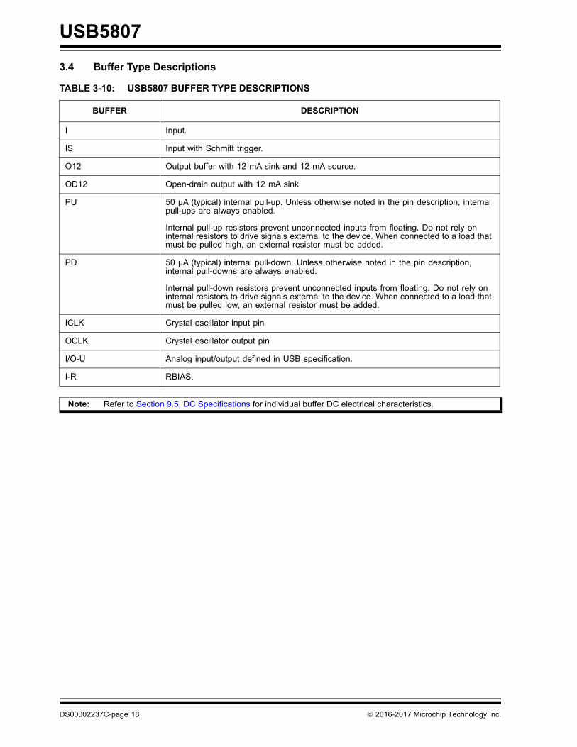
3.4 Buffer Type Descriptions
TABLE 3-10: USB5807 BUFFER TYPE DESCRIPTIONS
BUFFER DESCRIPTION
I Input.
IS Input with Schmitt trigger.
O12 Output buffer with 12 mA sink and 12 mA source.
OD12 Open-drain output with 12 mA sink
PU 50 μA (typical) internal pull-up. Unless otherwise noted in the pin description, internal pull-ups are always enabled.
Internal pull-up resistors prevent unconnected inputs from floating. Do not rely on internal resistors to drive signals external to the device. When connected to a load that must be pulled high, an external resistor must be added.
PD 50 μA (typical) internal pull-down. Unless otherwise noted in the pin description, internal pull-downs are always enabled.
Internal pull-down resistors prevent unconnected inputs from floating. Do not rely on internal resistors to drive signals external to the device. When connected to a load that must be pulled low, an external resistor must be added.
ICLK Crystal oscillator input pin
OCLK Crystal oscillator output pin
I/O-U Analog input/output defined in USB specification.
I-R RBIAS.
Note: Refer to Section 9.5, DC Specifications for individual buffer DC electrical characteristics.
DS00002237C-page 18 2016-2017 Microchip Technology Inc.

USB5807
3.5 Configuration Straps and Programmable Functions
Configuration straps are multi-function pins that are used during Power-On Reset (POR) or external chip reset(RESET_N) to determine the default configuration of a particular feature. The state of the signal is latched following de-assertion of the reset. Configuration straps are identified by an underlined symbol name. This section details the variousdevice configuration straps and associated programmable pin functions.
3.5.1 CFG_STRAP CONFIGURATION
The CFG_STRAP pin is used to place the hub into preset modes of operation. The resistor options are a 200 kΩ pull-down, 200 kΩ pull-up, 10 kΩ pull-down, 10 kΩ pull-up, 10 Ω pull-down, and 10 Ω pull-up as shown in Table 3-11.
Note: The system designer must guarantee that configuration straps meet the timing requirements specified inSection 9.6.2, Power-On and Configuration Strap Timing and Section 9.6.3, Reset and Configuration StrapTiming. If configuration straps are not at the correct voltage level prior to being latched, the device maycapture incorrect strap values.
TABLE 3-11: CFG_STRAP RESISTOR ENCODING
CFG_STRAP Resistor Value
Config Setting
200 kΩ Pull-Down CONFIG1 Speed Indicator Mode + SMBus Interface Disabled
The SMBus interface will be disabled.
The following programmable pins will be re-purposed as USB Speed Indicator outputs:
Pin 63: SPEED_IND1Pin 61: SPEED_IND2Pin 56: SPEED_IND3Pin 60: SPEED_IND4Pin 50: SPEED_IND5Pin 71: SPEED_IND6Pin 55: SPEED_IND7
The SPEED_INDx pins operate in the following manner:
Tri-state: Not connected0: USB 2.0 / USB 1.11: USB 3.1 Gen 1
2016-2017 Microchip Technology Inc. DS00002237C-page 19

USB5807
3.5.2 PORT DISABLE CONFIGURATION (PRT_DIS_P[7:1] / PRT_DIS_M[7:1])
The PRT_DIS_P[7:1] and PRT_DIS_M[7:1] configuration straps are used in conjunction to disable the related port (7-1).
For PRT_DIS_Px (where x is the corresponding port 7-1):
0 = Port x D+ Enabled
1 = Port x D+ Disabled
For PRT_DIS_Mx (where x is the corresponding port 7-1):
0 = Port x D- Enabled
1 = Port x D- Disabled
200 kΩ Pull-Up CONFIG2 Speed Indicator Mode + SMBus Slave Mode
The SMBus interface will operate in Slave Mode for use with hub configuration.
The following programmable pins will be re-purposed as USB Speed Indicator outputs:
Pin 63: SPEED_IND1Pin 61: SPEED_IND2Pin 56: SPEED_IND3Pin 60: SPEED_IND4Pin 50: SPEED_IND5Pin 71: SPEED_IND6Pin 55: SPEED_IND7
The SPEED_INDx pins operate in the following manner:
Tri-state: Not connected0: USB 2.0 / USB 1.11: USB 3.1 Gen 1
10 kΩ Pull-Down CONFIG3 Unused, Reserved
10 kΩ Pull-Up CONFIG4 Unused, Reserved
10 Ω Pull-Down CONFIG5 Battery Charging Indicator Mode
The following programmable pins will be re-purposed as USB Battery Charging Indicator outputs:
Pin 63: BC_IND1Pin 61: BC_IND2Pin 56: BC_IND3Pin 60: BC_IND4Pin 50: BC_IND5Pin 71: BC_IND6Pin 55: BC_IND7
The BC_INDx pins operate in the following manner:
Tri-state: Battery Charging not enabled0: Battery Charging enabled and successful BC handshake has occurred.1: Battery Charging enabled, but no BC handshake has occurred.
10 Ω Pull-Up CONFIG6 Unused, Reserved
TABLE 3-11: CFG_STRAP RESISTOR ENCODING (CONTINUED)
CFG_STRAP Resistor Value
Config Setting
DS00002237C-page 20 2016-2017 Microchip Technology Inc.

USB5807
3.5.3 NON-REMOVABLE PORT CONFIGURATION (CFG_NON_REM)
The CFG_NON_REM configuration strap is used to configure the non-removable port settings of the device to one offive settings. These modes are selected by the configuration of an external resistor on the CFG_NON_REM pin. Theresistor options are a 200 kΩ pull-down, 200 kΩ pull-up, 10 kΩ pull-down, 10 kΩ pull-up, 10 Ω pull-down and 10 Ω pull-up as shown in Table 3-12.
3.5.4 BATTERY CHARGING CONFIGURATION (CFG_BC_EN)
The CFG_BC_EN configuration strap is used to configure the battery charging port settings of the device to one of fivesettings. These modes are selected by the configuration of an external resistor on the CFG_BC_EN pin. The resistoroptions are a 200 kΩ pull-down, 200 kΩ pull-up, 10 kΩ pull-down, 10 kΩ pull-up, 10 Ω pull-down and 10 Ω pull-up asshown in Table 3-13.
3.5.5 GENERAL PURPOSE INPUT/OUTPUT CONFIGURATION (GPIOx)
General Purpose Inputs/Outputs may be used for application specific purposes. Any given GPIO may operate as aninput or an output. Inputs can apply an internal 50kΩ pull-down or pull-up resistor. Outputs may drive low or drive high(3.3V). GPIOs may be configured and manipulated via SMBus.
3.5.5.1 SMBus configuration
The SMBus slave interface may be used to write to internal registers that configure the state of the GPIO. Refer to the“Configuration Options for Microchip USB58xx and USB59xx Hubs” application note for additional details.
Note: Both PRT_DIS_Px and PRT_DIS_Mx (where x is the corresponding port) must be tied to 3.3 V to disablethe associated downstream port. Disabling the USB 2.0 port will also disable the corresponding USB 3.1Gen 1 port.
TABLE 3-12: CFG_NON_REM RESISTOR ENCODING
CFG_NON_REM Resistor Value Setting
200 kΩ Pull-Down All ports removable
200 kΩ Pull-Up Port 1 non-removable
10 kΩ Pull-Down Port 1, 2 non-removable
10 kΩ Pull-Up Port 1, 2, 3, non-removable
10 Ω Pull-Down Port 1, 2, 3, 4 non-removable
10 Ω Pull-Up Port 1, 2, 3, 4, 5, 6, 7 non-removable
TABLE 3-13: CFG_BC_EN RESISTOR ENCODING
CFG_BC_EN Resistor Value Setting
200 kΩ Pull-Down No battery charging
200 kΩ Pull-Up Port 1 battery charging
10 kΩ Pull-Down Port 1, 2 battery charging
10 kΩ Pull-Up Port 1, 2, 3, battery charging
10 Ω Pull-Down Port 1, 2, 3, 4 battery charging
10 Ω Pull-Up Port 1, 2, 3, 4, 5, 6, 7 battery charging
2016-2017 Microchip Technology Inc. DS00002237C-page 21

USB5807
DS00002237C-page 22 2016-2017 Microchip Technology Inc.
4.0 DEVICE CONNECTIONS
4.1 Power Connections
Figure 4-1 illustrates the device power connections.
4.2 SPI ROM Connections
Figure 4-2 illustrates the device SPI ROM connections. Refer to Section 7.1 “SPI Master Interface” for additional infor-mation on this device interface.
4.3 SMBus Slave Connections
Figure 4-3 illustrates the device SMBus slave connections. Refer to Section 7.2 “SMBus Slave Interface” for addi-tional information on this device interface.
FIGURE 4-1: DEVICE POWER CONNECTIONS
FIGURE 4-2: SPI ROM CONNECTIONS
FIGURE 4-3: SMBUS SLAVE CONNECTIONS
+3.3V Supply
USB5807
3.3V Internal LogicVDD33
VSS
1.2V Internal Logic
+1.2V Supply
VDD12
USB5807
SPI_CE_N
SPI_CLK
SPI_DO
SPI_DI
SPI ROM
CE#
CLK
DI
DO
+3.3V
USB5807SMCLK
SMDAT
SMBusMaster
Clock
Data
10K
+3.3V
10K

USB5807
5.0 MODES OF OPERATION
The device provides two main modes of operation: Standby Mode and Hub Mode. These modes are controlled via theRESET_N pin, as shown in Table 5-1.
The flowchart in Figure 5-1 details the modes of operation and how the device traverses through the Hub Mode stages(shown in bold). The remaining sub-sections provide more detail on each stage of operation.
TABLE 5-1: MODES OF OPERATION
RESET_N Input Summary
0 Standby Mode: This is the lowest power mode of the device. No functions are active other than monitoring the RESET_N input. All port interfaces are high impedance and the PLL is halted. Refer to Section 8.4.2, External Chip Reset (RESET_N) for additional information on RESET_N.
1 Hub (Normal) Mode: The device operates as a configurable USB hub with battery charger detection. This mode has various sub-modes of operation, as detailed in Figure 5-1. Power consumption is based on the number of active ports, their speed, and amount of data transferred.
FIGURE 5-1: HUB BOOT FLOWCHART
(OTP_CFG)
NORMAL operation
(SOC_CFG)
NO
YES
(STRAP)
SPISignaturePresent?
NO
YES
Load Config fromInternal ROM
(CFG_RD)
Modify ConfigBased on OTP
YES
(SPI_INIT)
CFG_STRAP for SMBus Slave?
SOC Done?
Do SMBus or I2C initialization
No
Combine OTP Config Data
Run from External ROM
Hub Connect
Load Config fromExternal ROM
(Ext_CFG_RD)
Modify ConfigBased on psuedo-
OTP
RESET_N deasserted
2016-2017 Microchip Technology Inc. DS00002237C-page 23

USB5807
5.1 Standby Mode
If the RESET_N pin is asserted, the hub will be in Standby Mode. This mode provides a very low power state for maxi-mum power efficiency when no signaling is required. This is the lowest power state. In Standby Mode all downstreamports are disabled, the USB data pins are held in a high-impedance state, all transactions immediately terminate (nostates saved), all internal registers return to their default state, the PLL is halted, and core logic is powered down in orderto minimize power consumption. Because core logic is powered off, no configuration settings are retained in this modeand must be re-initialized after RESET_N is negated high.
5.2 SPI Initialization Stage (SPI_INIT)
The first stage, the initialization stage, occurs on the deassertion of RESET_N. In this stage, the internal logic is reset,the PLL locks if a valid clock is supplied, and the configuration registers are initialized to their default state. The internalfirmware then checks for an external SPI ROM. The firmware looks for an external SPI flash device that contains a validsignature of “2DFU” (device firmware upgrade) beginning at address 0xFFFA. If a valid signature is found, then theexternal ROM is enabled and the code execution begins at address 0x0000 in the external SPI device. If a valid signa-ture is not found, then execution continues from internal ROM (CFG_RD stage).
When using an external SPI ROM, a 1 Mbit, 60 MHz or faster ROM must be used. Both 1- and 2-bit SPI operation aresupported. For optimum throughput, a 2-bit SPI ROM is recommended. Both mode 0 and mode 3 SPI ROMs are alsosupported.
If the system is not strapped for SPI Mode, code execution will continue from internal ROM (CFG_RD stage).
5.3 Configuration Read Stage (CFG_RD)
In this stage, the internal firmware loads the default values from the internal ROM and then uses the configuration strap-ping options to override the default values. Refer to Section 3.5, Configuration Straps and Programmable Functions forinformation on usage of the various device configuration straps.
5.4 Strap Read Stage (STRAP)
In this stage, the firmware registers the configuration strap settings and checks the state of CFG_STRAP. IfCFG_STRAP is set for CONFIG2, then the hub will check the state of the SMBDATA and SMBCLK pins. If 10k pull-upresistors are detected on both pins, the device will enter the SOC_CFG stage. If 10k pull-up resistors are not detectedon both pins, the hub will transition to the OTP_CFG stage instead.
5.5 SOC Configuration Stage (SOC_CFG)
In this stage, the SOC can modify any of the default configuration settings specified in the integrated ROM, such as USBdevice descriptors and port electrical settings.
There is no time limit on this mode. In this stage the firmware will wait indefinitely for the SMBus/I2C configuration. Whenthe SOC has completed configuring the device, it must write to register 0xFF to end the configuration.
5.6 OTP Configuration Stage (OTP_CFG)
Once the SOC has indicated that it is done with configuration, all configuration data is combined in this stage. Thedefault data, the SOC configuration data, and the OTP data are all combined in the firmware and the device is pro-grammed.
After the device is fully configured, it will go idle and then into suspend if there is no VBUS or Hub.Connect present.Once VBUS is present, and battery charging is enabled, the device will transition to the Battery Charger DetectionStage. If VBUS is present, and battery charging is not enabled, the device will transition to the Connect stage.
5.7 Hub Connect Stage (Hub.Connect)
Once the CHGDET stage is completed, the device enters the Hub Connect stage. USB connect can be initiated byasserting the VBUS pin function high. The device will remain in the Hub Connect stage indefinitely until the VBUS pinfunction is deasserted.
DS00002237C-page 24 2016-2017 Microchip Technology Inc.

USB5807
5.8 Normal Mode
Lastly, the hub enters Normal Mode of operation. In this stage full USB operation is supported under control of the USBHost on the upstream port. The device will remain in the normal mode until the operating mode is changed by the sys-tem.
2016-2017 Microchip Technology Inc. DS00002237C-page 25

USB5807
DS00002237C-page 26 2016-2017 Microchip Technology Inc.
6.0 DEVICE CONFIGURATION
The device supports a large number of features (some mutually exclusive), and must be configured in order to correctlyfunction when attached to a USB host controller. The hub can be configured either internally or externally depending onthe implemented interface.
Microchip provides a comprehensive software programming tool, Pro-Touch2, for configuring the USB5807 functions,registers and OTP memory. All configuration is to be performed via the Pro-Touch2 programming tool. For additionalinformation on the Pro-Touch2 programming tool, refer to Software Libraries within Microchip USB5807 product pageat www.microchip.com/USB5807.
6.1 Customer Accessible Functions
The following functions are available to the customer via the Pro-Touch2 Programming Tool.
6.1.1 USB ACCESSIBLE FUNCTIONS
6.1.1.1 SPI Access over USB
Access to an attached SPI device is performed as a pass-through operation from the USB Host. The device firmwarehas no knowledge of the operation of the attached SPI device. For more information, refer to the Microchip USB5807product page and SDK at www.microchip.com/USB5807.
6.1.1.2 OTP Access
The OTP ROM in the device is accessible via the USB bus during normal runtime operation or SMBus during theSOC_CFG stage. For more information, refer to the Microchip USB5807product page or the Pro-Touch2 User’s Guide.
6.1.1.3 Battery Charging Access over USB
The Battery charging behavior of the device can be dynamically changed by the USB Host when something other thanthe preprogrammed or OTP programmed behavior is desired. For more information, refer to the MicrochipUSB5807product page or the Pro-Touch2 User’s Guide.
6.1.2 SMBUS ACCESSIBLE FUNCTIONS
OTP access and configuration of specific device functions are possible via the USB5807 SMBus slave interface. All OTPparameters can be modified via the SMBus Host. For more information refer to the Microchip USB5807 product page.
Note: Device configuration straps and programmable pins are detailed in Section 3.5, Configuration Straps andProgrammable Functions.Refer to Section 7.0, Device Interfaces for detailed information on each device interface.
Note: For additional programming details, refer to the Pro-Touch2 programming tool User’s Guide.
Note: Refer to Section 7.1, SPI Master Interface for additional information on the SPI.
2016-2017 Microchip Technology Inc. DS00002237C-page 27
USB5807
7.0 DEVICE INTERFACES
The USB5807 provides multiple interfaces for configuration and external memory access. This section details the vari-ous device interfaces and their usage:
• SPI Master Interface
• SMBus Slave Interface
7.1 SPI Master Interface
The device is capable of code execution from an external SPI ROM. When configured for SPI Mode, on power up thefirmware looks for an external SPI flash device that contains a valid signature of 2DFU (device firmware upgrade) begin-ning at address 0xFFFA. If a valid signature is found, then the external ROM is enabled and the code execution beginsat address 0x0000 in the external SPI device. If a valid signature is not found, then execution continues from internalROM.
7.2 SMBus Slave Interface
The device includes an integrated SMBus slave interface, which can be used to access internal device run time registersor program the internal OTP memory. SMBus slave detection is accomplished by setting the CFG_STRAP in the correctconfiguration followed by detection of pull-up resistors on both the SMDAT and SMCLK signals during the hub’s boot-up sequence. Refer to Section 3.5.1, CFG_STRAP Configuration for additional information.
Note: For details on how to enable each interface, refer to Section 3.5, Configuration Straps and ProgrammableFunctions.
For information on device connections, refer to Section 4.0, Device Connections. For information on deviceconfiguration, refer to Section 6.0, Device Configuration.
Microchip provides a comprehensive software programming tool, Pro-Touch2, for configuring the USB5807functions, registers and OTP memory. All configuration is to be performed via the Pro-Touch2 programmingtool. For additional information on the Pro-Touch2 programming tool, refer to Software Libraries withinMicrochip USB5807 product page at www.microchip.com/USB5807.
Note: For SPI timing information, refer to Section 9.6.7, SPI Timing.
Note: All configuration is to be performed via the Pro-Touch2 programming tool. For additional information on thePro-Touch2 programming tool, refer to Software Libraries within Microchip USB5807 product page atwww.microchip.com/USB5807.

USB5807
8.0 FUNCTIONAL DESCRIPTIONS
This section details various USB5807 functions, including:
• USB Type-C Receptacle Support
• Battery Charging
• FlexConnect
• Resets
• Link Power Management (LPM)
• Remote Wakeup Indicator
• Port Control Interface
• Port Split
8.1 USB Type-C Receptacle Support
The USB5807 has built-in support for the USB Type-C receptacle.
8.1.1 EXTERNAL USB 3.1 GEN 1 MULTIPLEXER
C_ATTACH[0:3] pins are used to signal to the hub when a valid USB Type-C connection has been detected. This func-tionality requires an external USB Type-C controller such as a Microchip UTC2000 to monitor the USB Type-C recep-tacle for a valid attach. This signal is used to enable and disable clocking to the USB 3.1 Gen 1 PHY in order to reducepower consumption when there is no USB Type-C attach.
The C_ATTACH[0:3] pins are active high inputs. A high signal enables clocking to the PHY to enable a USB 3.1 Gen 1connection. A low signal disables the PHY.
A diagram of a USB Type-C Downstream Facing Port with a USB5807, Microchip UTC2000, and external multiplexeris shown in Figure 8-1.
A diagram of a USB Type-C Upstream Facing Port with a USB5807, Microchip UTC2000, and external multiplexer isshown in Figure 8-2.
FIGURE 8-1: DFP TYPE-C PORT WITH MICROCHIP UTC2000 AND EXTERNAL MUX
UTC2000DFP Mode
ENABLE
VBUS
SSTXA+SSTXA-
SSRXA+SSRXA-
SSTXB+SSTXB-
SSRXB+SSRXB-
D+D-
CC1CC2OCS#
CC1CC2
GENERICPORT PWR
CTLR
POWER
OCS
PPC_EN
MUX
SSTXA+SSTXA-
SSRXA+SSRXA-
SSTXB+SSTXB-
SSRXB+SSRXB-
SSTX+SSTX-
SSRX+SSRX-
PLUG_ORIENTATION#
A/B
USB Type-CUSB Type-C
External MuxDownstream Port
SSTX+SSTX-
SSRX+SSRX-
D+D-
PRT_CTLx
C_ATTACHx
DS00002237C-page 28 2016-2017 Microchip Technology Inc.

USB5807
8.2 Battery Charging
The device can be configured by an OEM to have any of the downstream ports support battery charging. The hub’s rolein battery charging is to provide acknowledgment to a device’s query as to whether the hub system supports USB batterycharging. The hub silicon does not provide any current or power FETs or any additional circuitry to actually charge thedevice. Those components must be provided externally by the OEM.
If the OEM provides an external supply capable of supplying current per the battery charging specification, the hub canbe configured to indicate the presence of such a supply from the device. This indication, via the PRT_CTL[7:1] pins, ison a per port basis. For example, the OEM can configure two ports to support battery charging through high currentpower FETs and leave the other two ports as standard USB ports.
For additional information, refer to the Microchip USB5807 Battery Charging application note on the Microchip.comUSB5807 product page www.microchip.com/USB5807.
FIGURE 8-2: UFP TYPE-C PORT WITH MICROCHIP UTC2000 & EXTERNAL MUX
FIGURE 8-3: BATTERY CHARGING EXTERNAL POWER SUPPLY
UTC2000UFP Mode
USB Type-CExternal Mux
Upstream PortVBUS
SSTXA+SSTXA-
SSRXA+SSRXA-
SSTXB+SSTXB-
SSRXB+SSRXB-
D+D-
CC1CC2
CC1CC2
CONNECTED#
MUX
VBUS_DET
SSTX+SSTX-
SSRX+SSRX-
D+D-
C_ATTACH0
SSTXA+SSTXA-
SSRXA+SSRXA-
SSTXB+SSTXB-
SSRXB+SSRXB-
SSTX+SSTX-
SSRX+SSRX-
USB Type-C
3.3VPLUG_
ORIENTATION#
A/B
SOC
VBUS[n]
INT
SCL
SDAMicrochip
Hub
DC Power
2016-2017 Microchip Technology Inc. DS00002237C-page 29
USB5807
8.3 FlexConnect
This feature allows the upstream port to be swapped with downstream physical port 1. Only downstream port 1 can beswapped physically. The default state is when port 0 is the upstream port. The ‘flexed” state is when port 1 is theupstream port.
FlexConnect can be enabled/disabled in any of the following ways:
• SMBus Configuration
• Direct Pin Control
8.3.1 SMBUS CONFIGURATION
FlexConnect can be controlled via runtime configuration registers through the SMBus Slave Interface during hub run-time (after enumeration).
8.3.2 DIRECT PIN CONTROL
The FLEX_CMD control input can be used to control the FlexConnect state. When driven or pulled low, the hub will operate in it’s default state. When driven or pull high, the hub will operate in it’s “flexed” state.
The FLEX_STATE output displays the current state of FlexConnect. It operates in the same manner regardless of how FlexConnect is controlled (SMBus or Direct Pin Control). When low, the hub is currently in it’s default state. When high, the hub is in its “flexed” state.
8.4 Resets
• Power-On Reset (POR)
• External Chip Reset (RESET_N)
• USB Bus Reset
8.4.1 POWER-ON RESET (POR)
A power-on reset occurs whenever power is initially supplied to the device, or if power is removed and reapplied to thedevice. A timer within the device will assert the internal reset per the specifications listed in Section 9.6.2, Power-Onand Configuration Strap Timing.
8.4.2 EXTERNAL CHIP RESET (RESET_N)
A valid hardware reset is defined as assertion of RESET_N, after all power supplies are within operating range, per thespecifications in Section 9.6.3, Reset and Configuration Strap Timing. While reset is asserted, the device (and its asso-ciated external circuitry) enters Standby Mode and consumes minimal current.
Assertion of RESET_N causes the following:
1. The PHY is disabled and the differential pairs will be in a high-impedance state.
2. All transactions immediately terminate; no states are saved.
3. All internal registers return to the default state.
4. The external crystal oscillator is halted.
5. The PLL is halted.
Note: For additional information, refer to the Microchip USB58xx/USB59xx FlexConnect application note on theMicrochip.com USB5807 product page.
Note: All power supplies must have reached the operating levels mandated in Section 9.2, Operating Condi-tions**, prior to (or coincident with) the assertion of RESET_N.
DS00002237C-page 30 2016-2017 Microchip Technology Inc.

USB5807
8.4.3 USB BUS RESET
In response to the upstream port signaling a reset to the device, the device performs the following:
1. Sets default address to 0.
2. Sets configuration to Unconfigured.
3. Moves device from suspended to active (if suspended).
4. Complies with the USB Specification for behavior after completion of a reset sequence.
The host then configures the device in accordance with the USB Specification.
8.5 Link Power Management (LPM)
The device supports the L0 (On), L1 (Sleep), and L2 (Suspend) link power management states. These supported LPMstates offer low transitional latencies in the tens of microseconds versus the much longer latencies of the traditional USBsuspend/resume in the tens of milliseconds. The supported LPM states are detailed in Table 8-1.
8.6 Remote Wakeup Indicator
The remote wakeup indicator feature uses SUSP_IND as a side band signal to wake up the host when in USB 2.0 sus-pend. This feature is enabled and disabled via the HUB_RESUME_INHIBIT configuration bit in the hub configurationspace register HUB_CFG_3. The only way to control the bit is by configuration EEPROM, SMBus or internal ROMdefault setting. The state is only modified during a power on reset, or hardware reset. No dynamic reconfiguring of thiscapability is possible.
When HUB_RESUME_INHIBIT = ‘0’, Normal Resume Behavior per the USB 2.0 specification
When HUB_RESUME_INHIBIT = ‘1’, Modified Resume Behavior is enabled
8.7 Port Control Interface
Port power and over-current sense share the same pin (PRT_CTLx) for each port. These functions can be controlleddirectly from the USB hub, or via the processor. Additionally, smart port controllers can be controlled via the I2C inter-face.
The device can be configured into one of the two following port control modes:
• Ganged Mode - A single GANG_PWR pin controls power and detects over-current events for all downstream ports.
• Individual Mode - Each port has an individual PRT_CTLx pin for independent port power control and over-current detection.
Port connection in various modes are detailed in the following subsections.
Note: The device does not propagate the upstream USB reset to downstream devices.
TABLE 8-1: LPM STATE DEFINITIONS
State Description Entry/Exit Time to L0
L2 Suspend Entry: ~3 msExit: ~2 ms (from start of RESUME)
L1 Sleep Entry: <10 usExit: <50 us
L0 Fully Enabled (On) -
Note: The SUSP_IND signal only indicates the USB2.0 state.
2016-2017 Microchip Technology Inc. DS00002237C-page 31
USB5807
8.7.1 PORT CONNECTION IN GANGED MODE
Ganged Mode is enabled via SMBus or OTP configuration. GANG_PWR becomes the port control (PRTCTL) pin for alldownstream ports when the hub is configured for ganged port power control mode. All port power controllers should becontrolled from this pin when the hub is configured for ganged port power mode. While in this mode of operation, anover-current event on any single downstream port will cause all downstream ports to be flagged for over-current.
8.7.2 PORT CONNECTION IN INDIVIDUAL MODE
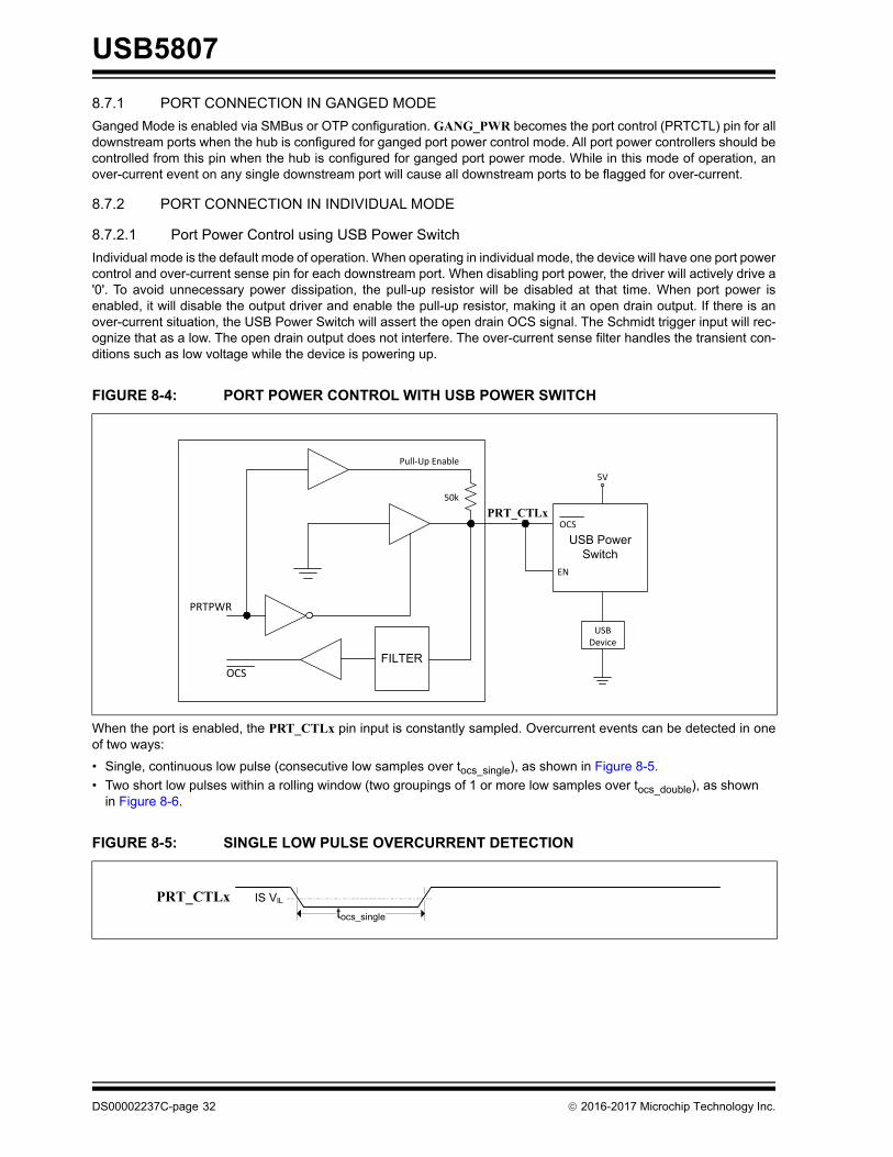
8.7.2.1 Port Power Control using USB Power Switch
Individual mode is the default mode of operation. When operating in individual mode, the device will have one port powercontrol and over-current sense pin for each downstream port. When disabling port power, the driver will actively drive a'0'. To avoid unnecessary power dissipation, the pull-up resistor will be disabled at that time. When port power isenabled, it will disable the output driver and enable the pull-up resistor, making it an open drain output. If there is anover-current situation, the USB Power Switch will assert the open drain OCS signal. The Schmidt trigger input will rec-ognize that as a low. The open drain output does not interfere. The over-current sense filter handles the transient con-ditions such as low voltage while the device is powering up.
When the port is enabled, the PRT_CTLx pin input is constantly sampled. Overcurrent events can be detected in oneof two ways:
• Single, continuous low pulse (consecutive low samples over tocs_single), as shown in Figure 8-5.
• Two short low pulses within a rolling window (two groupings of 1 or more low samples over tocs_double), as shown in Figure 8-6.
FIGURE 8-4: PORT POWER CONTROL WITH USB POWER SWITCH
FIGURE 8-5: SINGLE LOW PULSE OVERCURRENT DETECTION
USB Power Switch
50k
PRTPWR
EN
OCS
OCS
Pull‐Up Enable
5V
USB Device
FILTER
PRT_CTLx
PRT_CTLx IS VIL
tocs_single
DS00002237C-page 32 2016-2017 Microchip Technology Inc.

USB5807
To maximize compatibility with various port power control topologies, the parameters tocs_single and tocs_double are con-figurable via the Overcurrent Minimum Pulse Width Register and Overcurrent Inactive Timer Register.
The pin also has a turn-on “lockout” feature where the state of the pin is ignored for a configured amount of time imme-diately after port power is turned on. This prevents slow ramp times due to parasitic resistance/capacitance attached tothe pin from triggering false overcurrent detections. This parameter is configurable via the Overcurrent Lockout TimerRegister.
FIGURE 8-6: DOUBLE LOW PULSE OVERCURRENT DETECTION
TABLE 8-2: OVERCURRENT MINIMUM PULSE WIDTH REGISTER
OCS_MIN_WIDTH(30EAh)
Overcurrent Detection Pulse Window
BIT Name R/W Description
7:4 Reserved R Reserved
3:0 OCS_MIN_WIDTH R/W The minimum overcurrent detection pulse width (tocs_single) is config-ured in this register.
The range can be configured in 1ms increments from 0ms to 5ms.
0000 - 0ms minimum overcurrent detection pulse width0001 - 1ms minimum overcurrent detection pulse width0010 - 2ms minimum overcurrent detection pulse width0011 - 3ms minimum overcurrent detection pulse width0100 - 4ms minimum overcurrent detection pulse width0101 - 5ms minimum overcurrent detection pulse width [Default]
TABLE 8-3: OVERCURRENT INACTIVE TIMER REGISTER
OCS_INACTIVE_TIMER(30EBh)
Overcurrent Inactive Timer After First Overcurrent Detection
BIT Name R/W Description
7:0 OCS_INACTIVE_TIMER R/W This register configures the timer within which a double low pulse trig-gers an overcurrent detection event (tocs_double).
The timer can be incremented in 1ms steps. The default value is 20ms (14h).
Note: This register should never be set to 00h.
PRT_CTLx IS VIL
tocs_double
2016-2017 Microchip Technology Inc. DS00002237C-page 33

USB5807
8.7.2.2 Port Power Control using Poly Fuse
When using the device with a poly fuse, there is no need for an output power control. To maintain consistency, the samecircuit will be used. A single port power control and over-current sense for each downstream port is still used from theHub's perspective. When disabling port power, the driver will actively drive a '0'. This will have no effect as the externaldiode will isolate pin from the load. When port power is enabled, it will disable the output driver and enable the pull-upresistor. This means that the pull-up resistor is providing 3.3 volts to the anode of the diode. If there is an over-currentsituation, the poly fuse will open. This will cause the cathode of the diode to go to 0 volts. The anode of the diode willbe at 0.7 volts, and the Schmidt trigger input will register this as a low resulting in an over-current detection. The opendrain output does not interfere.
TABLE 8-4: OVERCURRENT LOCKOUT TIMER REGISTER
START_LOCKOUT_TIMER_REG(30E1h)
Start Lockout Timer Register
BIT Name R/W Description
7:0 START_LOCKOUT_TIMER_REG R/W The “start lockout timer” blocks an overcurrent event from being detected immediately after port power is turned on. Any overcurrent event within this timer value is ignored.
The timer can be incremented in 1ms steps. The default value is 10ms (0Ah).
Note: This register should never be set to 00h.
Note: The USB 2.0 and USB 3.1 Gen 1 bPwrOn2PwrGood descriptors must be set to 0 when using poly-fusemode. Refer to the “Configuration Options for the USB58xx and USB59xx” Microchip application note fordetails on how to change these values.
FIGURE 8-7: PORT POWER CONTROL USING A POLY FUSE
PRT_CTLx
50k
PRTPWR
OCS
USB Device
Pull-Up Enable
5V
Poly Fuse
FILTER
DS00002237C-page 34 2016-2017 Microchip Technology Inc.
USB5807
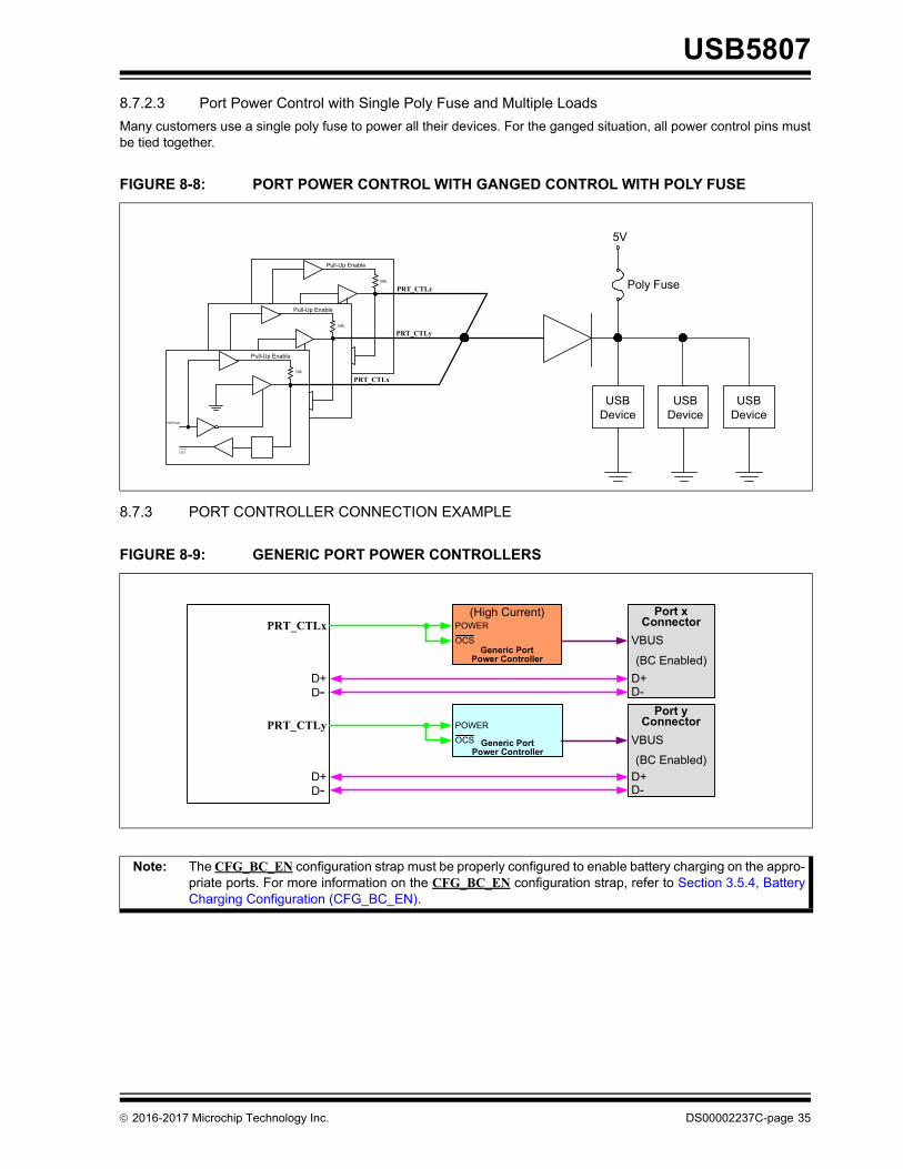
8.7.2.3 Port Power Control with Single Poly Fuse and Multiple Loads
Many customers use a single poly fuse to power all their devices. For the ganged situation, all power control pins mustbe tied together.
8.7.3 PORT CONTROLLER CONNECTION EXAMPLE
FIGURE 8-8: PORT POWER CONTROL WITH GANGED CONTROL WITH POLY FUSE
FIGURE 8-9: GENERIC PORT POWER CONTROLLERS
Note: The CFG_BC_EN configuration strap must be properly configured to enable battery charging on the appro-priate ports. For more information on the CFG_BC_EN configuration strap, refer to Section 3.5.4, BatteryCharging Configuration (CFG_BC_EN).
Pull-Up Enable
USBDevice
Poly Fuse
5V
Pull-Up Enable
Pull-Up Enable
50k
50k
50k
PRTPWR
OCS
USBDevice
USBDevice
PRT_CTLx
PRT_CTLy
PRT_CTLz
Generic Port Power Controller
Port xConnector
Generic Port Power Controller
POWER
(High Current)
(BC Enabled)
OCS
D+D-
VBUS
D+D-
Port yConnectorPOWER
(BC Enabled)
OCS
D+D-
VBUS
D+D-
PRT_CTLy
PRT_CTLx
2016-2017 Microchip Technology Inc. DS00002237C-page 35

USB5807
8.8 Port Split
8.8.1 FEATURE OVERVIEW
This feature allows the USB 2.0 and USB 3.1 Gen 1 PHYs associated with any downstream port to be operationallyseparated. The intention of this feature is to allow a system designer to connect an embedded USB 3.x device to theUSB 3.1 Gen 1 PHY, while allowing the USB 2.0 PHY to be used as either a standard USB 2.0 port or with a separateembedded USB 2.0 device.
This feature operates outside of the provisions of the USB specifications. Operation is intended for specialized applica-tions only. Contact your local sales representative for additional information.
In order to maintain a positive end user experience, it is recommended that only permanently attached, embedded USB3.x devices be connected to the USB 3.1 Gen 1 PHY when enabling the Port Split feature. This prevents end users fromattempting to connect USB High-Speed, Full-Speed, or Low-Speed devices to an exposed USB port which only has USB3.1 Gen 1 connections.
8.8.2 PORT SPLITTING CONFIGURATION
Downstream ports 5 and 6 may be configured for Port Splitting. Port Splitting is configured via register configurationthrough SMBus during the hub configuration stage (SOC_CFG) or via the hub’s internal OTP memory.
When Port Splitting is enabled, the existing PRT_CTLx pin associated with that port will continue to control the USB 2.0portion of the port in an identical matter. A new pin function assigned to a GPIOx pin will be activated and configured tocontrol the USB 3.1 Gen 1 portion of the port. This new pin is named PRTPWRx_USB3_SPLIT where x indicates therespective port. Note that overcurrent detection is not supported on the PRTPWRx_USB3_SPLIT pin. These new pinsare assigned as shown in Table 8-5.
FIGURE 8-10: RECOMMENDED PORT SPLITTING CONFIGURATIONS
USBPowerSwitch
EN
OCS
5V
USB2.0 Device
USB58xx/USB59xx
PRTCTLxVBUS
Embedded USB3.x Device
ENPRTPWRx_USB3_SPLIT
(GPIOxx)
USB58xx/USB59xx
PRTCTLx
Embedded USB3.x Device
ENPRTPWRx_USB3_SPLIT
(GPIOxx)
Embedded USB2.0 Device
EN
DS00002237C-page 36 2016-2017 Microchip Technology Inc.
USB5807
8.8.2.1 Enabling Port Splitting
In order to enable the Port Splitting feature on downstream ports 5 and/or6, the following configuration settings must bemade.
Enabling Port Splitting on Port 5:
• Write 0x42 to register 0x416D to select GPIO66 for Option A
• Write 0x05 to register 0x416D to select GPIO5 for Option B
Enabling Port Splitting on Port 6:
• Write 0x06 to register 0x416E to select GPIO6 for Option A
• Write 0x04 to register 0x416E to select GPIO4 for Option B
8.8.2.2 Link Timeout Reset
Port Splitting is intended for use with embedded USB 3.x devices only. When Port Splitting is enabled, the hub constantlymonitors the USB 3.1 Gen 1 Link to see if a valid USB 3.1 Gen 1 Link is established. If there is no valid USB 3.1 Gen 1Link for a configured amount of time (see below), then the hub will toggle assertion of the associated “PRTPWRx-_USB3_SPLIT” pin in an attempt to reset the embedded USB 3.1 Gen 1 device and re-establish the USB 3.1 Gen 1 Link.The timer is always reset and restarted whenever the timeout occurs.
A valid USB 3.1 Gen 1 link is qualified by the LTSSM_STATE register status for the port. A normal Link will activelyswitch through many Link states.
If the hub detects that the Link is staying in one of the following Link states the entire duration of the timeout timer, thenthe Link is stuck in an invalid state and PRTPWRx_USB3_SPLIT will be toggled in order to attempt to re-establish theLink.
• SIS.Disabled(0x4)
• Rx.Detect(0x5)
• SS.Inactive(0x6)
• Polling(0x7)
• Recovery(0x8)
• HotReset (0x9)
The Link Timeout Reset value is configured via register 0x4171 and can be overridden by OTP. The default value is0x05, which selects a Timeout value of 1 second. Setting the register to 0x00 will disable the Link Timeout Reset feature.
The duration of the Link reset (time which PRTPWRx_USB3_SPLIT signal stays low) can be configured in register0x4176. The default duration is 400ms with a configurable range of 350ms to 2.9s.
TABLE 8-5: PORT SPLIT PRTPWRX_USB3_SPLIT PIN ASSIGNMENT
GPIOx Pin Port Split Assignment
GPIO66 PRTPWR5_USB3_SPLIT Option A
GPIO6 PRTPWR6_USB3_SPLIT Option A
GPIO5 PRTPWR5_USB3_SPLIT Option B
GPIO4 PRTPWR6_USB3_SPLIT Option B
2016-2017 Microchip Technology Inc. DS00002237C-page 37

USB5807
TABLE 8-6: USB 3.X PORT SPLIT LINK TIMEOUT REGISTER
USB3_PORT_SPLIT_TIMEOUT(0X4171 - RESET=0X05) USB 3.X PORT SPLIT LINK TIMEOUT REGISTER
BIT NAME R/W DESCRIPTION
[7:3] Reserved R/W Always read ‘0’
[2:0] PORT_SPLIT_TIMEOUT[2:0]
R/W Global USB Port Splitting Link Timeout Value
If Port Splitting is enabled on a port and there is no valid USB 3.x Link for the configured amount of time, then the associated “PRTPWRx_USB3_SPLIT” pin will be toggled in an attempt to reset the embedded USB 3.x device and re-establish the USB 3.x Link. The timer is always reset and restarted whenever the timeout occurs.
000b - No Timeout, never toggle PRTPWRx_USB3_SPLIT 001b - 100ms 010b - 250ms 011b - 500ms 100b - 750ms 101b - 1 second 110b - 2 second 111b - Reserved
TABLE 8-7: USB 3.X PORT SPLIT TOGGLE TIME REGISTER
USB3_PORT_SPLIT_TOGGLE_TIME(0X4176 - RESET=0X05) USB 3.X PORT SPLIT TOGGLE TIME REGISTER
BIT NAME R/W DESCRIPTION
[7:0] PORT_SPLIT_TOGGLE_TIME[7:0]
R/W The PORT_SPLIT_TOGGLE_TIME is used to control the length of time port power is toggled off. This is specific to the “PRTPWRx_USB3_SPLIT” pin, and is only used in conjunction with 0X4171. The timer is always reset whenever the toggle completes.
The minimum toggle time is 350ms and is represented by 00000000b.
Each incremental value will add 10ms to the 350ms minimum value.
DS00002237C-page 38 2016-2017 Microchip Technology Inc.
USB5807
9.0 OPERATIONAL CHARACTERISTICS
9.1 Absolute Maximum Ratings*
+1.2 V Supply Voltage (VDD12) (Note 1) . . . . . . . . . . . . . . . . . . . . . . . . . . . . . . . . . . . . . . . . . . . . . . . -0.5 V to +1.32 V
+3.3 V Supply Voltage (VDD33) (Note 1) . . . . . . . . . . . . . . . . . . . . . . . . . . . . . . . . . . . . . . . . . . . . . . . . -0.5 V to +4.6 V
Positive voltage on input signal pins, with respect to ground (Note 2) . . . . . . . . . . . . . . . . . . . . . . . . . . . . . . . . . +4.6 V
Negative voltage on input signal pins, with respect to ground . . . . . . . . . . . . . . . . . . . . . . . . . . . . . . . . . . . . . . . . -0.5 V
Positive voltage on XTALI/CLKIN, with respect to ground . . . . . . . . . . . . . . . . . . . . . . . . . . . . . . . . . . . . . . . . .+3.63 V
Positive voltage on USB DP/DM signal pins, with respect to ground . . . . . . . . . . . . . . . . . . . . . . . . . . . . . . . . . . .+6.0 V
Positive voltage on USB 3.1 Gen 1 USB3UP_xxxx and USB3DN_xxxx signal pins, with respect to ground . . . . .1.32 V
Storage Temperature . . . . . . . . . . . . . . . . . . . . . . . . . . . . . . . . . . . . . . . . . . . . . . . . . . . . . . . . . . . . . . .-55oC to +150oC
Junction Temperature . . . . . . . . . . . . . . . . . . . . . . . . . . . . . . . . . . . . . . . . . . . . . . . . . . . . . . . . . . . . . . . . . . . . . .+125oC
Lead Temperature Range . . . . . . . . . . . . . . . . . . . . . . . . . . . . . . . . . . . . . . . . . . . . . . Refer to JEDEC Spec. J-STD-020
HBM ESD Performance . . . . . . . . . . . . . . . . . . . . . . . . . . . . . . . . . . . . . . . . . . . . . . . . . . . . . . . . . . . . . . . . . . . . . . 3 kV
Note 1: When powering this device from laboratory or system power supplies, it is important that the absolute max-imum ratings not be exceeded or device failure can result. Some power supplies exhibit voltage spikes ontheir outputs when AC power is switched on or off. In addition, voltage transients on the AC power line mayappear on the DC output. If this possibility exists, it is suggested to use a clamp circuit.
Note 2: This rating does not apply to the following pins: All USB DM/DP pins, XTAL1/CLKIN, and XTALO
*Stresses exceeding those listed in this section could cause permanent damage to the device. This is a stress ratingonly. Exposure to absolute maximum rating conditions for extended periods may affect device reliability. Functionaloperation of the device at any condition exceeding those indicated in Section 9.2, Operating Conditions**, Section 9.5,DC Specifications, or any other applicable section of this specification is not implied.
9.2 Operating Conditions**
+1.2 V Supply Voltage (VDD12) . . . . . . . . . . . . . . . . . . . . . . . . . . . . . . . . . . . . . . . . . . . . . . . . . . . . . +1.08 V to +1.32 V
+3.3 V Supply Voltage (VDD33) . . . . . . . . . . . . . . . . . . . . . . . . . . . . . . . . . . . . . . . . . . . . . . . . . . . . . . . +3.0 V to +3.6 V
Input Signal Pins Voltage (Note 2) . . . . . . . . . . . . . . . . . . . . . . . . . . . . . . . . . . . . . . . . . . . . . . . . . . . . . -0.3 V to +3.6 V
XTALI/CLKIN Voltage . . . . . . . . . . . . . . . . . . . . . . . . . . . . . . . . . . . . . . . . . . . . . . . . . . . . . . . . . . . . . . -0.3 V to +3.6 V
USB 2.0 DP/DM Signal Pins Voltage . . . . . . . . . . . . . . . . . . . . . . . . . . . . . . . . . . . . . . . . . . . . . . . . . . . -0.3 V to +5.5 V
USB 3.1 Gen 1 USB3UP_xxxx and USB3DN_xxxx Signal Pins Voltage . . . . . . . . . . . . . . . . . . . . . . . -0.3 V to +1.32 V
Ambient Operating Temperature in Still Air (TA) . . . . . . . . . . . . . . . . . . . . . . . . . . . . . . . . . . . . . . . . . . . . . . . . . . .Note 3
+1.2 V Supply Voltage Rise Time (TRT in Figure 9-1) . . . . . . . . . . . . . . . . . . . . . . . . . . . . . . . . . . . . . . . . . . . . . . 400 µs
+3.3 V Supply Voltage Rise Time (TRT in Figure 9-1) . . . . . . . . . . . . . . . . . . . . . . . . . . . . . . . . . . . . . . . . . . . . . . 400 µs
Note 3: 0oC to +70oC for commercial version, -40oC to +85oC for industrial version.
**Proper operation of the device is guaranteed only within the ranges specified in this section.
Note: Do not drive input signals without power supplied to the device.
2016-2017 Microchip Technology Inc. DS00002237C-page 39

USB5807
9.3 Package Thermal Specifications
FIGURE 9-1: SUPPLY RISE TIME MODEL
Note: The rise time for the 3.3 V supply can be extended to 100ms max if RESET_N is actively driven low, typi-cally by another IC, until 1 µs after all supplies are within operating range.
TABLE 9-1: PACKAGE THERMAL PARAMETERS
Symbol °C/W Velocity (Meters/s)
JA19 0
16 1
JT0.1 0
0.1 1
JC1.4 0
1.4 1
Note: Thermal parameters are measured or estimated for devices in a multi-layer 2S2P PCB per JESDN51. Forindustrial applications, the USB5807 requires a multi-layer 2S4P PCB power dissipation.
TABLE 9-2: MAXIMUM POWER DISSIPATION
Parameter Value Units
PD(max) 2.3 W
t10%
10%
90%
Voltage TRT
t90% Time
100%3.3 V
VSS
VDD33
90%
100%1.2 VVDD12
DS00002237C-page 40 2016-2017 Microchip Technology Inc.

USB5807
9.4 Power Consumption
The values shown below represent typical power consumption as measured during various modes of operation. Powerdissipation is determined by temperature, supply voltage, and external source/sink requirements.
The following measurements were taken with VDD33 equal to 3.3V, VDD12 equal to 1.2V, at an ambient temperatureof 25°C.
Note: Actual power consumption will vary depending on the capabilities of the USB host, the devices connected,data type, and data bus utilization. The published data represents typical power consumption of the hub atnominal ambient temperature and supply voltage while large file transfers are active between USB host andUSB Mass Storage class devices on all downstream ports.
Typical power consumption for specific use cases can be estimated using the formulas below:
IVDD33(mA) = 35 + (NPORTSFS)(1)* +(NPORTSHS)(10) + (NPORTSSS)(7)IVDD12(mA) = 245+ (NPORTSFS)(0.1)* +(NPORTSHS)(2) + (NPORTSSS)(109)PTOTAL(mW) = 409.5+ (NPORTSFS)(3.42)* +(NPORTSHS)(35.4) + (NPORTSSS)(153.9)
9.5 DC Specifications
Note: A USB 3.x hub operates both the USB 3.x and USB 2.0 interfaces in parallel on it’s upstream port connec-tion. A port operating under the SS/HS condition indicates that a USB 3.x hub was connected to it.
TABLE 9-3: DEVICE POWER CONSUMPTION
Typical (mA) Typical Power
VDD33 VDD12 (mW)
Reset 0.5 27.5 28
No VBUS 0.7 21.5 28
Global Suspend 7.5 24.5 32
7 FS Ports 42 246 433
7 HS Ports 105 259 657
7 SS Ports 84 1,008 1,487
7 SS/HS Ports 514 1,022 1,735
TABLE 9-4: I/O DC ELECTRICAL CHARACTERISTICS
Parameter Symbol Min Typical Max Units Notes
I Type Input Buffer
Low Input Level
High Input Level
VIL
VIH 2.1
0.9 V
V
IS Type Input Buffer
Low Input Level
High Input Level
Schmitt Trigger Hysteresis (VIHT - VILT)
VIL
VIH
VHYS
1.9
9 20
0.9
40
V
V
mV
O6 Type Output Buffer
Low Output Level
High Output Level
VOL
VOH VDD33-0.4
0.4 V
V
IOL = 6 mA
IOH = -6 mA
2016-2017 Microchip Technology Inc. DS00002237C-page 41

USB5807
Note 4: XTALI can optionally be driven from a 25 MHz singled-ended clock oscillator.
Note 5: Refer to the USB 3.1 Gen 1 Specification for USB DC electrical characteristics.
9.6 AC Specifications
This section details the various AC timing specifications of the device.
9.6.1 POWER SUPPLY AND RESET_N SEQUENCE TIMING
Figure 9-2 illustrates the recommended power supply sequencing and timing for the device. VDD33 should rise after orat the same rate as VDD12. Similarly, RESET_N and/or VBUS_DET should rise after or at the same rate as VDD33.VBUS_DET and RESET_N do not have any other timing dependencies.
O12 Type Output Buffer
Low Output Level
High Output Level
VOL
VOH VDD33-0.4
0.4 V
V
IOL = 12 mA
IOH = -12 mA
OD12 Type Output Buffer
Low Output Level VOL 0.4 V IOL = 12 mA
ICLK Type Input Buffer(XTALI Input)
Low Input Level
High Input Level
VIL
VIH 0.85
0.50
VDD33
V
V
Note 4
IO-U Type Buffer(See Note 5)
Note 5
FIGURE 9-2: POWER SUPPLY AND RESET_N SEQUENCE TIMING
TABLE 9-5: POWER SUPPLY AND RESET_N SEQUENCE TIMING
Symbol Description Min Typ Max Units
tVDD33 VDD12 to VDD33 rise time 0 ms
treset VDD33 to RESET_N/VBUS_DET rise time 0 ms
TABLE 9-4: I/O DC ELECTRICAL CHARACTERISTICS (CONTINUED)
Parameter Symbol Min Typical Max Units Notes
VDD12
VDD33
RESET_N/VBUS_DET
DS00002237C-page 42 2016-2017 Microchip Technology Inc.

USB5807
9.6.2 POWER-ON AND CONFIGURATION STRAP TIMING
Figure 9-3 illustrates the configuration strap valid timing requirements in relation to power-on, for applications whereRESET_N is not used at power-on. In order for valid configuration strap values to be read at power-on, the followingtiming requirements must be met. The operational levels (Vopp) for the external power supplies are detailed inSection 9.2, Operating Conditions**.
Device configuration straps are also latched as a result of RESET_N assertion. Refer to Section 9.6.3, Reset and Con-figuration Strap Timing for additional details.
9.6.3 RESET AND CONFIGURATION STRAP TIMING
Figure 9-4 illustrates the RESET_N pin timing requirements and its relation to the configuration strap pins. Assertion ofRESET_N is not a requirement. However, if used, it must be asserted for the minimum period specified. Refer toSection 8.4, Resets for additional information on resets. Refer to Section 3.5, Configuration Straps and ProgrammableFunctions for additional information on configuration straps.
FIGURE 9-3: POWER-ON CONFIGURATION STRAP VALID TIMING
TABLE 9-6: POWER-ON CONFIGURATION STRAP LATCHING TIMING
Symbol Description Min Typ Max Units
tcsh Configuration strap hold after external power supplies at opera-tional levels
1 ms
FIGURE 9-4: RESET_N CONFIGURATION STRAP TIMING
TABLE 9-7: RESET_N CONFIGURATION STRAP TIMING
Symbol Description Min Typ Max Units
trstia RESET_N input assertion time 5 s
tcsh Configuration strap pins hold after RESET_N deassertion 1 ms
Note: The clock input must be stable prior to RESET_N deassertion.
Configuration strap latching and output drive timings shown assume that the Power-On reset has finishedfirst otherwise the timings in Section 9.6.2, Power-On and Configuration Strap Timing apply.
All External Power Supplies
Vopp
Configuration Straps
RESET_N
Configuration Straps
trstia
tcsh
2016-2017 Microchip Technology Inc. DS00002237C-page 43

USB5807
9.6.4 USB TIMING
All device USB signals confirm to the voltage, power, and timing characteristics/specifications as set forth in the Univer-sal Serial Bus Specification. Please refer to the Universal Serial Bus Revision 3.1 Specification, available at http://www.usb.org/developers/docs.
9.6.5 I2C TIMING
All device I2C signals confirm to the 100KHz Standard Mode (Sm) voltage, power, and timing characteristics/specifica-tions as set forth in the I2C-Bus Specification. Please refer to the I2C-Bus Specification, available at http://www.nxp.com/documents/user_manual/UM10204.pdf.
9.6.6 SMBUS TIMING
All device SMBus signals confirm to the voltage, power, and timing characteristics/specifications as set forth in the Sys-tem Management Bus Specification. Please refer to the System Management Bus Specification, Version 1.0, availableat http://smbus.org/specs.
9.6.7 SPI TIMING
This section specifies the SPI timing requirements for the device.
FIGURE 9-5: SPI TIMING
TABLE 9-8: SPI TIMING (30 MHZ OPERATION)
Symbol Description Min Typ Max Units
tfc Clock frequency 30 MHz
tceh Chip enable (SPI_CE_EN) high time 100 ns
tclq Clock to input data 13 ns
tdh Input data hold time 0 ns
tos Output setup time 5 ns
toh Output hold time 5 ns
tov Clock to output valid 4 ns
tcel Chip enable (SPI_CE_EN) low to first clock 12 ns
tceh Last clock to chip enable (SPI_CE_EN) high 12 ns
SPI_CLK
SPI_DI
SPI_DO
SPI_CE_N
tcel tfc
tclq
tceh
tdh
tohtostov toh
DS00002237C-page 44 2016-2017 Microchip Technology Inc.

USB5807
9.7 Clock Specifications
The device can accept either a 25MHz crystal or a 25MHz single-ended clock oscillator (±50ppm) input. If the single-ended clock oscillator method is implemented, XTALO should be left unconnected and XTALI/CLKIN should be drivenwith a nominal 0-3.3V clock signal. The input clock duty cycle is 40% minimum, 50% typical and 60% maximum.
It is recommended that a crystal utilizing matching parallel load capacitors be used for the crystal input/output signals(XTALI/XTALO). The following circuit design (Figure 9-6) and specifications (Table 9-10) are required to ensure properoperation.
9.7.1 CRYSTAL SPECIFICATIONS
It is recommended that a crystal utilizing matching parallel load capacitors be used for the crystal input/output signals(XTALI/XTALO). Refer to Table 9-10 for the recommended crystal specifications.
TABLE 9-9: SPI TIMING (60 MHZ OPERATION)
Symbol Description Min Typ Max Units
tfc Clock frequency 60 MHz
tceh Chip enable (SPI_CE_EN) high time 50 ns
tclq Clock to input data 9 ns
tdh Input data hold time 0 ns
tos Output setup time 5 ns
toh Output hold time 5 ns
tov Clock to output valid 4 ns
tcel Chip enable (SPI_CE_EN) low to first clock 12 ns
tceh Last clock to chip enable (SPI_CE_EN) high 12 ns
FIGURE 9-6: 25MHZ CRYSTAL CIRCUIT
TABLE 9-10: CRYSTAL SPECIFICATIONS
PARAMETER SYMBOL MIN NOM MAX UNITS NOTES
Crystal Cut AT, typ
Crystal Oscillation Mode Fundamental Mode
Crystal Calibration Mode Parallel Resonant Mode
Frequency Ffund - 25.000 - MHz
Frequency Tolerance @ 25oC Ftol - - ±50 PPM
Frequency Stability Over Temp Ftemp - - ±50 PPM
Frequency Deviation Over Time Fage - ±3 to 5 - PPM Note 6
XTALO
XTALI
Y1
C1 C2
2016-2017 Microchip Technology Inc. DS00002237C-page 45

USB5807
Note 6: Frequency Deviation Over Time is also referred to as Aging.
Note 7: 0 °C for commercial version, -40 °C for industrial version.
Note 8: +70 °C for commercial version, +85 °C for industrial version.
Note 9: This number includes the pad, the bond wire and the lead frame. PCB capacitance is not included in thisvalue. The XTALI/CLKIN pin, XTALO pin and PCB capacitance values are required to accurately calculatethe value of the two external load capacitors. These two external load capacitors determine the accuracy ofthe 25.000 MHz frequency.
9.7.2 EXTERNAL REFERENCE CLOCK (CLKIN)
When using an external reference clock, the following input clock specifications are suggested:
• 25 MHz
• 50% duty cycle ±10%, ±100 ppm
• Jitter < 100 ps RMS
Total Allowable PPM Budget - - ±100 PPM Note 7
Shunt Capacitance CO - 7 typ - pF
Load Capacitance CL - 20 typ - pF
Drive Level PW 100 - - uW
Equivalent Series Resistance R1 - - 60 Ω
Operating Temperature Range Note 7 - Note 8 oC
XTALI/CLKIN Pin Capacitance - 3 typ - pF Note 9
XTALO Pin Capacitance - 3 typ - pF Note 9
TABLE 9-10: CRYSTAL SPECIFICATIONS (CONTINUED)
PARAMETER SYMBOL MIN NOM MAX UNITS NOTES
DS00002237C-page 46 2016-2017 Microchip Technology Inc.
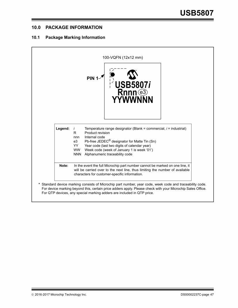
USB5807
10.0 PACKAGE INFORMATION
10.1 Package Marking Information
* Standard device marking consists of Microchip part number, year code, week code and traceability code.For device marking beyond this, certain price adders apply. Please check with your Microchip Sales Office.For QTP devices, any special marking adders are included in QTP price.
Legend: i Temperature range designator (Blank = commercial, i = industrial)R Product revisionnnn Internal codee3 Pb-free JEDEC® designator for Matte Tin (Sn)YY Year code (last two digits of calendar year)WW Week code (week of January 1 is week ‘01’)NNN Alphanumeric traceability code
Note: In the event the full Microchip part number cannot be marked on one line, itwill be carried over to the next line, thus limiting the number of availablecharacters for customer-specific information.
100-VQFN (12x12 mm)
PIN 1
USB5807iRnnn e3
YYWWNNNe3
2016-2017 Microchip Technology Inc. DS00002237C-page 47

USB5807
10.2 Package Drawings
Note: For the most current package drawings, see the Microchip Packaging Specification at: http://www.microchip.com/packaging.
FIGURE 10-1: 100-VQFN PACKAGE (DRAWING)
DS00002237C-page 48 2016-2017 Microchip Technology Inc.

USB5807
FIGURE 10-2: 100-VQFN PACKAGE (DIMENSIONS)
Notes:
2016-2017 Microchip Technology Inc. DS00002237C-page 49

USB5807
FIGURE 10-3: 100-VQFN PACKAGE (LAND PATTERN)
RECOMMENDED LAND PATTERN
Dimension LimitsUnits
C2
Optional Center Pad Width
Contact Pad Spacing
Optional Center Pad Length
Contact Pitch
Y2X2
8.108.10
MILLIMETERS
0.40 BSCMIN
EMAX
11.70
Contact Pad Length (X100)Contact Pad Width (X100)
Y1X1
1.050.20
Microchip Technology Drawing C04-2407A
NOM
SILK SCREEN
1 2
100
C1
C2
E
X1
Y1
G1
Y2
X2
C1Contact Pad Spacing 11.70
Contact Pad to Center Pad (X100) G1 0.20Thermal Via Diameter VThermal Via Pitch EV
0.331.20
ØV
EV
EV
BSC: Basic Dimension. Theoretically exact value shown without tolerances.
Notes:Dimensioning and tolerancing per ASME Y14.5M
For best soldering results, thermal vias, if used, should be filled or tented to avoid solder loss duringreflow process
1.
2.
DS00002237C-page 50 2016-2017 Microchip Technology Inc.

2016-2017 Microchip Technology Inc. DS00002237C-page 51
USB5807
APPENDIX A: REVISION HISTORY
TABLE A-1: REVISION HISTORY
Revision Level & Date Section/Figure/Entry Correction
DS00002237C (08-18-17) Figure 10-1, Figure 10-2, Figure 10-3 Updated package drawings.
Section 3.2, Pin Symbols, Figure 3-1, Table 3-4
Removed references to PRT_CTL0 pin.
Table 9-10 Updated max equivalent series resistance to 60Ω.
Table 9-3 Updated values.
DS00002237B (01-20-17)Figure 4-2, SPI ROM Connections Modified drawing by changing position of DO
to DI and DI to DO
Table 9-3, Device Power Consump-tion
Typical power consumption formula added below table.
Section 8.8.2.1, Enabling Port Split-ting
Options A and B added.
Throughout data sheet Changed 62kOhm to 50kOhm
Table 3-1, Pin Reset State Legend In PD-15k, changed “Hardware enables inter-nal 62kOhm pull-down” to “Hardware enables internal 15kOhm pull-down”
Table 3-7, Miscellaneous Pin Descrip-tions
Removed the following description for the SMBus/I2C Clock and SMBus/I22C:“..or I2C bridge dependent on the device con-figuration.”
DS00002237A (10-03-16) All Initial Release

USB5807
DS00002237C-page 52 2016-2017 Microchip Technology Inc.
Note the following details of the code protection feature on Microchip devices:
• Microchip products meet the specification contained in their particular Microchip Data Sheet.
• Microchip believes that its family of products is one of the most secure families of its kind on the market today, when used in the intended manner and under normal conditions.
• There are dishonest and possibly illegal methods used to breach the code protection feature. All of these methods, to our knowledge, require using the Microchip products in a manner outside the operating specifications contained in Microchip’s Data Sheets. Most likely, the person doing so is engaged in theft of intellectual property.
• Microchip is willing to work with the customer who is concerned about the integrity of their code.
• Neither Microchip nor any other semiconductor manufacturer can guarantee the security of their code. Code protection does not mean that we are guaranteeing the product as “unbreakable.”
Code protection is constantly evolving. We at Microchip are committed to continuously improving the code protection features of ourproducts. Attempts to break Microchip’s code protection feature may be a violation of the Digital Millennium Copyright Act. If such actsallow unauthorized access to your software or other copyrighted work, you may have a right to sue for relief under that Act.
Information contained in this publication regarding device applications and the like is provided only for your convenience and may besuperseded by updates. It is your responsibility to ensure that your application meets with your specifications. MICROCHIP MAKES NOREPRESENTATIONS OR WARRANTIES OF ANY KIND WHETHER EXPRESS OR IMPLIED, WRITTEN OR ORAL, STATUTORY OROTHERWISE, RELATED TO THE INFORMATION, INCLUDING BUT NOT LIMITED TO ITS CONDITION, QUALITY, PERFORMANCE,MERCHANTABILITY OR FITNESS FOR PURPOSE. Microchip disclaims all liability arising from this information and its use. Use ofMicrochip devices in life support and/or safety applications is entirely at the buyer’s risk, and the buyer agrees to defend, indemnify andhold harmless Microchip from any and all damages, claims, suits, or expenses resulting from such use. No licenses are conveyed, implic-itly or otherwise, under any Microchip intellectual property rights unless otherwise stated.
Trademarks
The Microchip name and logo, the Microchip logo, AnyRate, AVR, AVR logo, AVR Freaks, BeaconThings, BitCloud, CryptoMemory, CryptoRF, dsPIC, FlashFlex, flexPWR, Heldo, JukeBlox, KEELOQ, KEELOQ logo, Kleer, LANCheck, LINK MD, maXStylus, maXTouch, MediaLB, megaAVR, MOST, MOST logo, MPLAB, OptoLyzer, PIC, picoPower, PICSTART, PIC32 logo, Prochip Designer, QTouch, RightTouch, SAM-BA, SpyNIC, SST, SST Logo, SuperFlash, tinyAVR, UNI/O, and XMEGA are registered trademarks of Microchip Technology Incorporated in the U.S.A. and other countries.
ClockWorks, The Embedded Control Solutions Company, EtherSynch, Hyper Speed Control, HyperLight Load, IntelliMOS, mTouch, Precision Edge, and Quiet-Wire are registered trademarks of Microchip Technology Incorporated in the U.S.A.
Adjacent Key Suppression, AKS, Analog-for-the-Digital Age, Any Capacitor, AnyIn, AnyOut, BodyCom, chipKIT, chipKIT logo, CodeGuard, CryptoAuthentication, CryptoCompanion, CryptoController, dsPICDEM, dsPICDEM.net, Dynamic Average Matching, DAM, ECAN, EtherGREEN, In-Circuit Serial Programming, ICSP, Inter-Chip Connectivity, JitterBlocker, KleerNet, KleerNet logo, Mindi, MiWi, motorBench, MPASM, MPF, MPLAB Certified logo, MPLIB, MPLINK, MultiTRAK, NetDetach, Omniscient Code Generation, PICDEM, PICDEM.net, PICkit, PICtail, PureSilicon, QMatrix, RightTouch logo, REAL ICE, Ripple Blocker, SAM-ICE, Serial Quad I/O, SMART-I.S., SQI, SuperSwitcher, SuperSwitcher II, Total Endurance, TSHARC, USBCheck, VariSense, ViewSpan, WiperLock, Wireless DNA, and ZENA are trademarks of Microchip Technology Incorporated in the U.S.A. and other countries.
SQTP is a service mark of Microchip Technology Incorporated in the U.S.A.
Silicon Storage Technology is a registered trademark of Microchip Technology Inc. in other countries.
GestIC is a registered trademark of Microchip Technology Germany II GmbH & Co. KG, a subsidiary of Microchip Technology Inc., in other countries.
All other trademarks mentioned herein are property of their respective companies.
© 2016-2017, Microchip Technology Incorporated, All Rights Reserved.
ISBN: 9781522420385
Microchip received ISO/TS-16949:2009 certification for its worldwide headquarters, design and wafer fabrication facilities in Chandler and Tempe, Arizona; Gresham, Oregon and design centers in California and India. The Company’s quality system processes and procedures are for its PIC® MCUs and dsPIC® DSCs, KEELOQ® code hopping devices, Serial EEPROMs, microperipherals, nonvolatile memory and analog products. In addition, Microchip’s quality system for the design and manufacture of development systems is ISO 9001:2000 certified.
QUALITYMANAGEMENTSYSTEMCERTIFIEDBYDNV
== ISO/TS16949==

2016-2017 Microchip Technology Inc. DS00002237C-page 53
USB5807
PRODUCT IDENTIFICATION SYSTEM
To order or obtain information, e.g., on pricing or delivery, refer to the factory or the listed sales office.
PART NO. [-X] /XX
PackageTemperatureRange
Device
Device: USB5807
Tape and Reel Option:
Blank = Standard packaging (tube or tray) T = Tape and Reel(1)
Temperature Range:
Blank = 0C to +70C (Commercial)I = -40C to +85C (Industrial)
Package: KD = 100-pin VQFN
Examples:
a) USB5807/KDTray, Commercial temp., 100-pin VQFN
b) USB5807-I/KDTray, Industrial temp., 100-pin VQFN
c) USB5807T/KDTape & reel, Commercial temp., 100-pin VQFN
d) USB5807T-I/KDTape & reel, Industrial temp., 100-pin VQFN
Note 1: Tape and Reel identifier only appears in the catalog part number description. This identifier is used for ordering purposes and is not printed on the device package. Check with your Microchip Sales Office for package availability with the Tape and Reel option.
[X](1)
Tape and ReelOption

USB5807
DS00002237C-page 54 2016-2017 Microchip Technology Inc.
THE MICROCHIP WEB SITE
Microchip provides online support via our WWW site at www.microchip.com. This web site is used as a means to makefiles and information easily available to customers. Accessible by using your favorite Internet browser, the web sitecontains the following information:
• Product Support – Data sheets and errata, application notes and sample programs, design resources, user’s guides and hardware support documents, latest software releases and archived software
• General Technical Support – Frequently Asked Questions (FAQ), technical support requests, online discussion groups, Microchip consultant program member listing
• Business of Microchip – Product selector and ordering guides, latest Microchip press releases, listing of seminars and events, listings of Microchip sales offices, distributors and factory representatives
CUSTOMER CHANGE NOTIFICATION SERVICE
Microchip’s customer notification service helps keep customers current on Microchip products. Subscribers will receivee-mail notification whenever there are changes, updates, revisions or errata related to a specified product family ordevelopment tool of interest.
To register, access the Microchip web site at www.microchip.com. Under “Support”, click on “Customer ChangeNotification” and follow the registration instructions.
CUSTOMER SUPPORT
Users of Microchip products can receive assistance through several channels:
• Distributor or Representative
• Local Sales Office
• Field Application Engineer (FAE)
• Technical Support
Customers should contact their distributor, representative or Field Application Engineer (FAE) for support. Local salesoffices are also available to help customers. A listing of sales offices and locations is included in the back of thisdocument.
Technical support is available through the web site at: http://microchip.com/support

2016-2017 Microchip Technology Inc. DS00002237C-page 55
AMERICASCorporate Office2355 West Chandler Blvd.Chandler, AZ 85224-6199Tel: 480-792-7200 Fax: 480-792-7277Technical Support: http://www.microchip.com/supportWeb Address: www.microchip.com
AtlantaDuluth, GA Tel: 678-957-9614 Fax: 678-957-1455
Austin, TXTel: 512-257-3370
BostonWestborough, MA Tel: 774-760-0087 Fax: 774-760-0088
ChicagoItasca, IL Tel: 630-285-0071 Fax: 630-285-0075
DallasAddison, TX Tel: 972-818-7423 Fax: 972-818-2924
DetroitNovi, MI Tel: 248-848-4000
Houston, TX Tel: 281-894-5983
IndianapolisNoblesville, IN Tel: 317-773-8323Fax: 317-773-5453Tel: 317-536-2380
Los AngelesMission Viejo, CA Tel: 949-462-9523Fax: 949-462-9608Tel: 951-273-7800
Raleigh, NC Tel: 919-844-7510
New York, NY Tel: 631-435-6000
San Jose, CA Tel: 408-735-9110Tel: 408-436-4270
Canada - TorontoTel: 905-695-1980 Fax: 905-695-2078
ASIA/PACIFICAsia Pacific OfficeSuites 3707-14, 37th FloorTower 6, The GatewayHarbour City, Kowloon
Hong KongTel: 852-2943-5100Fax: 852-2401-3431
Australia - SydneyTel: 61-2-9868-6733Fax: 61-2-9868-6755
China - BeijingTel: 86-10-8569-7000 Fax: 86-10-8528-2104
China - ChengduTel: 86-28-8665-5511Fax: 86-28-8665-7889
China - ChongqingTel: 86-23-8980-9588Fax: 86-23-8980-9500
China - DongguanTel: 86-769-8702-9880
China - GuangzhouTel: 86-20-8755-8029
China - HangzhouTel: 86-571-8792-8115 Fax: 86-571-8792-8116
China - Hong Kong SARTel: 852-2943-5100 Fax: 852-2401-3431
China - NanjingTel: 86-25-8473-2460Fax: 86-25-8473-2470
China - QingdaoTel: 86-532-8502-7355Fax: 86-532-8502-7205
China - ShanghaiTel: 86-21-3326-8000 Fax: 86-21-3326-8021
China - ShenyangTel: 86-24-2334-2829Fax: 86-24-2334-2393
China - ShenzhenTel: 86-755-8864-2200 Fax: 86-755-8203-1760
China - WuhanTel: 86-27-5980-5300Fax: 86-27-5980-5118
China - XianTel: 86-29-8833-7252Fax: 86-29-8833-7256
ASIA/PACIFICChina - XiamenTel: 86-592-2388138 Fax: 86-592-2388130
China - ZhuhaiTel: 86-756-3210040 Fax: 86-756-3210049
India - BangaloreTel: 91-80-3090-4444 Fax: 91-80-3090-4123
India - New DelhiTel: 91-11-4160-8631Fax: 91-11-4160-8632
India - PuneTel: 91-20-3019-1500
Japan - OsakaTel: 81-6-6152-7160 Fax: 81-6-6152-9310
Japan - TokyoTel: 81-3-6880- 3770 Fax: 81-3-6880-3771
Korea - DaeguTel: 82-53-744-4301Fax: 82-53-744-4302
Korea - SeoulTel: 82-2-554-7200Fax: 82-2-558-5932 or 82-2-558-5934
Malaysia - Kuala LumpurTel: 60-3-6201-9857Fax: 60-3-6201-9859
Malaysia - PenangTel: 60-4-227-8870Fax: 60-4-227-4068
Philippines - ManilaTel: 63-2-634-9065Fax: 63-2-634-9069
SingaporeTel: 65-6334-8870Fax: 65-6334-8850
Taiwan - Hsin ChuTel: 886-3-5778-366Fax: 886-3-5770-955
Taiwan - KaohsiungTel: 886-7-213-7830
Taiwan - TaipeiTel: 886-2-2508-8600 Fax: 886-2-2508-0102
Thailand - BangkokTel: 66-2-694-1351Fax: 66-2-694-1350
EUROPEAustria - WelsTel: 43-7242-2244-39Fax: 43-7242-2244-393
Denmark - CopenhagenTel: 45-4450-2828 Fax: 45-4485-2829
Finland - EspooTel: 358-9-4520-820
France - ParisTel: 33-1-69-53-63-20 Fax: 33-1-69-30-90-79
France - Saint CloudTel: 33-1-30-60-70-00
Germany - GarchingTel: 49-8931-9700Germany - HaanTel: 49-2129-3766400
Germany - HeilbronnTel: 49-7131-67-3636
Germany - KarlsruheTel: 49-721-625370
Germany - MunichTel: 49-89-627-144-0 Fax: 49-89-627-144-44
Germany - RosenheimTel: 49-8031-354-560
Israel - Ra’anana Tel: 972-9-744-7705
Italy - Milan Tel: 39-0331-742611 Fax: 39-0331-466781
Italy - PadovaTel: 39-049-7625286
Netherlands - DrunenTel: 31-416-690399 Fax: 31-416-690340
Norway - TrondheimTel: 47-7289-7561
Poland - WarsawTel: 48-22-3325737
Romania - BucharestTel: 40-21-407-87-50
Spain - MadridTel: 34-91-708-08-90Fax: 34-91-708-08-91
Sweden - GothenbergTel: 46-31-704-60-40
Sweden - StockholmTel: 46-8-5090-4654
UK - WokinghamTel: 44-118-921-5800Fax: 44-118-921-5820
Worldwide Sales and Service
11/07/16