Embed Size (px)
Citation preview
1Subject to change without notice.www.cree.com
60W Auxiliary Power Supply Demonstration board
CPW
R-A
N14,
REV -
60W
Auxi
liary
Pow
er S
upply
Dem
o b
oar
d
1. DEMONSTRATION BOARD SUMMARY
The CRD-060DD12P is a Cree demonstration board for a single-end Flyback converter design with acommercially available 1700V Silicon Carbide (SiC) MOSFET to replace conventional two-switchFlyback converter for high voltage input auxiliary power supply of three phase applications. Thedemonstration board is not designed to be a product and is to be only used as a tool to evaluate theperformance Cree switching devices.
2. INTRODUCTION
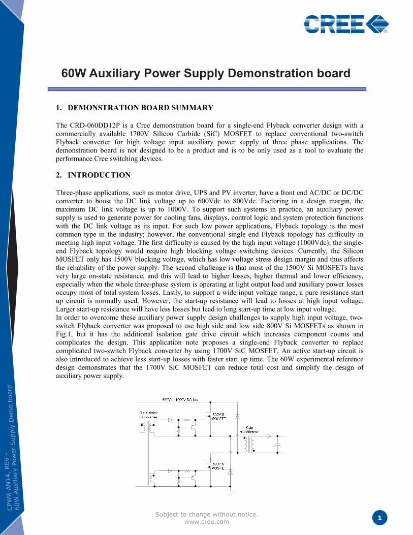
Three-phase applications, such as motor drive, UPS and PV inverter, have a front end AC/DC or DC/DCconverter to boost the DC link voltage up to 600Vdc to 800Vdc. Factoring in a design margin, themaximum DC link voltage is up to 1000V. To support such systems in practice, an auxiliary powersupply is used to generate power for cooling fans, displays, control logic and system protection functionswith the DC link voltage as its input. For such low power applications, Flyback topology is the mostcommon type in the industry; however, the conventional single end Flyback topology has difficulty inmeeting high input voltage. The first difficulty is caused by the high input voltage (1000Vdc); the single-end Flyback topology would require high blocking voltage switching devices. Currently, the SiliconMOSFET only has 1500V blocking voltage, which has low voltage stress design margin and thus affectsthe reliability of the power supply. The second challenge is that most of the 1500V Si MOSFETs havevery large on-state resistance, and this will lead to higher losses, higher thermal and lower efficiency,especially when the whole three-phase system is operating at light output load and auxiliary power lossesoccupy most of total system losses. Lastly, to support a wide input voltage range, a pure resistance startup circuit is normally used. However, the start-up resistance will lead to losses at high input voltage.Larger start-up resistance will have less losses but lead to long start-up time at low input voltage.In order to overcome these auxiliary power supply design challenges to supply high input voltage, two-switch Flyback converter was proposed to use high side and low side 800V Si MOSFETs as shown inFig.1, but it has the additional isolation gate drive circuit which increases component counts andcomplicates the design. This application note proposes a single-end Flyback converter to replacecomplicated two-switch Flyback converter by using 1700V SiC MOSFET. An active start-up circuit isalso introduced to achieve less start-up losses with faster start up time. The 60W experimental referencedesign demonstrates that the 1700V SiC MOSFET can reduce total cost and simplify the design ofauxiliary power supply.
Figure 1: A conventional two-switch Flyback converter with 800V Si MOSFET

2CPWR-AN14, REV -60W Auxiliary Power Supply Demo board
This document is provided for informational purposes only and is not a warranty or a specification. For product specifications, please see the data sheets available at www.cree.com/power. For warranty information, please contact Cree Sales at [email protected].
3. Cree 1700V SiC MOSFET
Today, SiC devices are characterized by a number of promising properties like high rating voltages, lowswitching losses, low on-state resistance, higher operating temperature, and high radiation hardness. Acommercially available 1700V TO-247 packaged SiC MOSFET, C2M1000170D, from Cree Inc is usedfor a wide input auxiliary power supply application. The table compares the key parameters between SiCMOSFET and Si MOSFET with common TO-247 package. From this comparison, SiC MOSFET cansupport much higher blocking voltage to 1700V and avalanche voltage above 1800V, while Si MOSFETonly has 1500V blocking voltage with lower avalanche voltage. For the on-state resistance and parasiticcapacitance, the SiC MOSFET has lower value than Si MOSFET to have low conduction losses and lowswitching losses. This key difference will value 1700V SiC MOSFET to have high efficiency and highreliability replacing 1500V Si MOSFET.
Table 1: Parameter comparisons of 1700V SiC MOSFET and 1500V Si MOSFET
Parameters SiC MOSFET
C2M1000170D
Si MOS
STW4N150
Si MOS
2SK2225DS
V(BR)DSS 1700V 1500V 1500V
Avalanche >1800V N/A N/A
Id @ Tc=25°C 5A 4A 2A
Rdson @150°C 2ohm 9ohm 20ohm
Coss 14pF 120pF 60pF
Tjmax >150°C 150°C 150°C
Package TO-247 TO-220, TO-247 TO-3PF
4. ACTIVE START-UP CIRCUIT
In this design, a non-dissipative, active start-up circuit has been implemented to optimize converterefficiency and fast start-up time. The alternative is to use a pure resistive start-up circuit whichsignificantly affects converter efficiency and start up times at low input voltages in a negative way. Figure2 shows the proposed active start-up circuit. When input voltage is increasing, Q6 is turned on by Vbasefrom path R31 to R36. The VCC voltage comes from path R22 to R25 when U1 (UCC28C44) is turningon. Once U1 starts operating, the VCC supply comes from the primary auxiliary winding. When VCCreaches the startup threshold of U1, the VREF (+5V) goes to high and Q7 is turned on. And then Q6 isturned off, which disconnects the start-up current path to VCC. The R31 to R36 resistors with large valueare used as the voltage balancing for input capacitors C1 to C3. The startup resistors R22 to R25 feeds thePWM controller of U1 until the auxiliary supply voltage rises and is disconnected from VCC of U1 andthen there are no more losses from start-up resistors. So the active start-up circuit can reduce the start uppower dissipation, especially at high line input voltage and improve the efficiency. The additional powerdissipation under such normal steady state conditions is due to the balance resistances, and they can be setat very high values (>6Mohm). More importantly, due to low resistance values for this active start-upcircuit, the start-up time will be short and can be trimmed to meet targeting start-up time. If assumingminimum start-up time 1s, the VCC capacitance can be calculated as follows:
offUVLOonUVLO
upstartupstartCUCCupstart VV
TIC
__
4428
(1)

3CPWR-AN14, REV -60W Auxiliary Power Supply Demo board
This document is provided for informational purposes only and is not a warranty or a specification. For product specifications, please see the data sheets available at www.cree.com/power. For warranty information, please contact Cree Sales at [email protected].
From datasheet of UCC28C44: mAI upstartCUCC 1.04428 ; VV onUVLO 5.14_ ; VV offUVLO 0.9_ . If FC upStart 18
,
it can select the VCC capacitance is 22uF. The total start-up current may then be calculated using the
below equation:
mAS
VFT
VCI
upstart
onUVLOupstartupstart 319.0
15.1422_
(2)
Hence, the total start-up resistors (R22 to R25) may be calculated as:
KmA
VVI
VVR
upstart
offUVLODCupstart 600
319.09200_min
(3)
Assuming worse darlington gain FEh is 500, the total balance resistance (R31-R36) may be calculated as:
MmA
VVhI
VVR
FEupstart
offUVLODCBalance 300
319.09200
/_min
(4)
By using much higher balance resistance, total additional losses can be seen to have no negative impact
on total losses.
Figure 2: The proposed active start-up circuit
C210uF
J1
HV_DC
1
+ C36NC
C110uF
+ C1222uF
U1
UCC28C44
COMP1
FB2
CS3
RC4
GND5
OUT6
VCC7
VREF8
R22150k
R35
1M5
R30
510k
+ C1010uF
ZD318V
R474.7k
R331M5
Q6STP03D200
R23150k
C310uF
R341M5
R24150k
C110.1uF
Q5PBSS4240T
R36
1M5
Q7MMBT2222A
R321M5
R311M5
C130.1uF
R25150kJ2
P_GND
1
VCC
HV_DC
450V
I/P:200Vto 1000V
450V
450V

4CPWR-AN14, REV -60W Auxiliary Power Supply Demo board
This document is provided for informational purposes only and is not a warranty or a specification. For product specifications, please see the data sheets available at www.cree.com/power. For warranty information, please contact Cree Sales at [email protected].
5. EXPERIMENTAL RESULTS
To demonstrate high performance ofsupply with proposed active start
Table 2: 60W auxiliary
Input Voltage
Output Voltage
Output Current
Frequency
Efficiency
Figure 3:
Figure 4:
75.0%
76.0%
77.0%
78.0%
79.0%
80.0%
81.0%
82.0%
83.0%
84.0%
85.0%
200v
Effi
cie
ncy
(%)
EXPERIMENTAL RESULTS
high performance of 1700V SiC MOSFET, a 60W single-end Flybacksupply with proposed active start-up circuit is developed as shown in Figure 3.
auxiliary SMPS prototype design specification with 1700V SiC MOSFET
Input Voltage 200Vdc to 1000Vdc
Voltage +12Vdc +5Vdc -12Vdc
Output Current 4.5A 0.5A 0.25A
Frequency 75KHz
Efficiency >83%
: Photo of 60W auxiliary SMPS with 1700V SiC MOSFET
: 60W auxiliary SMPS efficiency with 1700V SiC MOSFET
400v 600v 800v
Vin (Vdc)
CREE C2M1000170D
ST STW4N150
end Flyback auxiliary power
with 1700V SiC MOSFET
1000V

5CPWR-AN14, REV -60W Auxiliary Power Supply Demo board
This document is provided for informational purposes only and is not a warranty or a specification. For product specifications, please see the data sheets available at www.cree.com/power. For warranty information, please contact Cree Sales at [email protected].
Figure 4 compares measured efficiency at full load with input voltage varying from 200V to 1000V usingdifferent Si and SiC devices. Due to lower on-state resistance and parasitic capacitance, the 1700V SiCMOSFET can achieve a higher efficiency when compared to other 1500V Si MOSFET competitors.Thermal comparison at full load with the same heat sink is shown in Fig.5, SiC MOSFET clearly shows alower operating temperature at 45.9°C when compared to Si 1500V MOS at 60°C and 99.9°C. It showsthat 1700V SiC MOSFET can achieve higher reliability. Use of the 1700V SiC MOSFET also allows usto use a small low cost heat sink due to the fact that a smaller amount of heat needs to be dissipated asshown in Figure 6. This can save the auxiliary power board size and improve power density.
(a) SiC MOS C2M1000170D (b) Si MOS STW4N150 (c) Si MOS 2SK2225
Figure 5: Thermal comparison with same large heat sink and input voltage is 1000Vdc
Figure 6: SiC MOSFET Thermal with small low cost heatsink and input voltage is 1000Vdc
Figure 7 shows the start up waveform with the proposed active start-up circuit. At 1000Vdc input, start uptime is less 100ms and at 200Vdc input, start up time is less than 1s. Meanwhile, by trimming the start-upresistor R22 to R25, it can achieve faster start up time smoothly without sacrificing efficiency.
(a) 1000V input full load (b) 200V input full load
Figure 7: Start-up sequence waveforms
C2 (pink): Vin, 350V/Div; C3 (blue): Vcc, 10V/Div; C4 (green):Vgs, 20V/Div
C2M1000170D with large heat sink STW4N150 with large heat sink 2SK2225 with large heat sink
C2M1000170D with small heat sink

6CPWR-AN14, REV -60W Auxiliary Power Supply Demo board
This document is provided for informational purposes only and is not a warranty or a specification. For product specifications, please see the data sheets available at www.cree.com/power. For warranty information, please contact Cree Sales at [email protected].
Figure 8 shows the Vgs and Vds waveforms at difference input voltage and output loading (full load andlight load). It shows that 1700V SiC MOSFET Vgs and Vds waveforms are very clean with fast switchingat 200Vdc and 1000Vdc inputs.
(a) Input: 200Vdc, Light load (b) Input: 200Vdc, Full load
(c) Input: 1000Vdc, Light load (d) Input: DC 1000V, Full load
Figure 8: Vgs and Vds waveforms of 1700V SiC MOSFET
C1(yellow): Vgs, 10V/div; C4 (green): Vds, 500V/div
REFERENCES
[1] C2M1000170D 1700V SiC MOSFET datasheet, Cree InC.[2] JinBin Zhao, and FengZhi Dai, “Soft-switching two-switch flyback converter with wide range,” in Industrial
Electronics and Application, 2008. ICIEA 2008.[3] Robert W, Dragan M, Fundamentals of Power Electronics, Boulder Colorado, 2002.[4] Lloyd H. Dixon, “Magnetics Design for Switching Power Supplies,” in Unitrode Magnetics Design Handbook, 1990.[5] Bob Callanan. Application Considerations for Silicon Carbide MOSFETs, Cree InC.

7CPWR-AN14, REV -60W Auxiliary Power Supply Demo board
This document is provided for informational purposes only and is not a warranty or a specification. For product specifications, please see the data sheets available at www.cree.com/power. For warranty information, please contact Cree Sales at [email protected].
Appendix A – Schematic

8CPWR-AN14, REV -60W Auxiliary Power Supply Demo board
This document is provided for informational purposes only and is not a warranty or a specification. For product specifications, please see the data sheets available at www.cree.com/power. For warranty information, please contact Cree Sales at [email protected].
Appendix B - BOM
Partno.
Value Manufacturer Part no.Manufacturer
nameDescription
1 C1 10uF B32794D2106K EPCOS MKP, 5%
2 C2 10uF B32794D2106K EPCOS MKP, 5%
3 C3 10uF B32794D2106K EPCOS MKP, 5%
4 C4 0.1uF CAP CER 100V 10% X7R 0603
5 C5 680uF EEU-HD1V681 Panasonic
6 C6 0.1uF CAP CER 100V 10% X7R 0603
7 C7 1.2nF ECW-H16122JV Panasonic
8 C8 100pF CAP CER 100V 10% X7R 0603
9 C9 1uF CAP CER 100V 10% X7R 1206
10 C10 10uF ECEA1HKS100 Panasonic
11 C11 0.1uF CAP CER 100V 10% X7R 1206
12 C12 22uF EEA-GA1V220 Panasonic
13 C13 0.1uF CAP CER 100V 10% X7R 0603
14 C14 22nF CAP CER 100V 10% X7R 0603
15 C15 1nF CAP CER 100V 10% C0G 0603
16 C16 0.1uF CAP CER 100V 10% X7R 0603
17 C17 NC
18 C18 10nF CAP CER 100V 10% X7R 0603
19 C19 680uF EEU-HD1V681 Panasonic
20 C20 100nF CAP CER 100V 10% X7R 0603
21 C21 100uF UPB1V101MPD Nichicon
22 C22 1uF CAP CER 50V 10% X7R 0603
23 C23 100nF CAP CER 100V 10% X7R 0603
24 C24 220uF EEU-EB1V221 Panasonic
25 C25 0.1uF CAP CER 100V 10% X7R 0603
26 C26 1uF CAP CER 50V 10% X7R 0603
27 C27 47uF EEA-GA1V470 Panasonic
28 C28 1uF CAP CER 50V 10% X7R 0603
29 C29 0.22uF R76TR3220SE30K Kamet
30 C30 220uF EEU-EB1V221 Panasonic
31 C31 0.1uF CAP CER 100V 10% X7R 0603
32 C32 0.1uF CAP CER 100V 10% X7R 0603
33 C33 47uF EEA-GA1V470 Panasonic
34 C34 1uF CAP CER 50V 10% X7R 0603
35 C35 100pF CAP CER 100V 10% X7R 0603
36 C36 NC
37 C37 10nF CAP CER 100V 10% X7R 0603
38 C38 1uF CAP CER 50V 10% X7R 0603
39 C39 100pF CAP CER 100V 10% C0G 1206
40 C40 33pF CAP CER 100V 10% C0G 1206
41 C41 33pF CAP CER 100V 10% C0G 1206
42 D1 RS1M-13-F Diodes
43 D2 STTH1R02A ST
44 D3 1N4148
45 D4 VB30100S-E3/8W Vishay
46 D5 STPS3H100U ST
47 D6 STPS3H100U ST
48 D7 RS1M-13-F Diodes
49 D8 1N4148
50 D9 1N4148
51 D10 1N4148
52 J1 HV_DC 2 pin, P:5.08mm HV tips terminal
53 J2 P_GND 2 pin, P:5.08mm HV tips terminal
54 J3 CON2 282837-2 TE Horizontal, P:5.08mm
55 J4 CON2 282837-2 TE Horizontal, P:5.08mm
56 J5 CON2 282837-2 TE Horizontal, P:5.08mm
57 L1 3.5uH 744771003 Wurth
58 L2 2.7uH SWPA5020S2R7NT Sunlord
59 L3 2.7uH SWPA5020S2R2NT Sunlord
60 Q1 1000mohm, 1700V C2M1000170D CREE 1700V, 1000mohm, SiC MOSFET
61 Q4 PBSS4240T NXP

9CPWR-AN14, REV -60W Auxiliary Power Supply Demo board
This document is provided for informational purposes only and is not a warranty or a specification. For product specifications, please see the data sheets available at www.cree.com/power. For warranty information, please contact Cree Sales at [email protected].
62 Q5 PBSS4240T NXP
63 Q6 STP03D200 ST
64 Q7 MMBT2222A
65 R1 220K 1W, 1%
66 R2 10R RES, 0.25W, 1%, 1206
67 R3 2k2 RES, 0.25W, 1%, 1206
68 R4 1R3 CRCW25121R30FP Vishay 1W, 1%
69 R5 1R3 CRCW25121R30FP Vishay 1W, 1%
70 R6 220K 1W, 1%
71 R7 1R RES, 0.25W, 1%, 1206
72 R8 NC
73 R9 11k RES, 0.1W, 1%, 0603
74 R12 0 RES, 0.1W, 1%, 0603
75 R13 10k RES, 0.1W, 1%, 0603
76 R14 0 RES, 0.1W, 1%, 0603
77 R15 NC
78 R16 1k RES, 0.1W, 1%, 0603
79 R17 33k RES, 0.1W, 1%, 0603
80 R18 39k RES, 0.1W, 1%, 0603
81 R19 10k RES, 0.1W, 1%, 0603
82 R20 2K RES, 0.1W, 1%, 0603
83 R21 10k RES, 0.25W, 1%, 1206
84 R22 150k RES, 0.5W, 200V, 1%
85 R23 150k RES, 0.5W, 200V, 1%
86 R24 150k RES, 0.5W, 200V, 1%
87 R25 150k RES, 0.5W, 200V, 1%
88 R26 0R RES, 0.5W, 200V, 1%
89 R27 0R RES, 0.5W, 200V, 1%
90 R28 0R RES, 0.5W, 200V, 1%
91 R29 0R RES, 0.5W, 200V, 1%
92 R30 510K RES, 0.25W, 1%, 1206
93 R31 1M5 RES, 0.5W, 200V, 1%
94 R32 1M5 RES, 0.5W, 200V, 1%
95 R33 1M5 RES, 0.5W, 200V, 1%
96 R34 1M5 RES, 0.5W, 200V, 1%
97 R35 1M5 RES, 0.5W, 200V, 1%
98 R36 1M5 RES, 0.5W, 200V, 1%
99 R37 10k RES, 0.25W, 1%, 1206
100 R38 10k RES, 0.25W, 1%, 1206
101 R39 2.4k RES, 0.1W, 1%, 0603
102 R40 5.6k RES, 0.1W, 1%, 0603
103 R41 NC
104 R42 220K 1W, 1%
105 R43 220K 1W, 1%
106 R44 33 RES, 0.5W, 200V, 1%
107 R45 10k RES, 0.1W, 1%, 0603
108 R46 0 RES, 0.5W, 100V, 1%
109 R47 4.7k RES, 0.1W, 1%, 0603
110 R50 51R RES, 0.25W, 1%, 1206
111 R51 36R RES, 0.25W, 1%, 1206
112 R52 36R RES, 0.25W, 1%, 1206
113 R53 10R RES, 0.25W, 1%, 1206
114 T1 PQ26/25 750341672 Würth-midcom PQ2625 transformer
115 U1 UCC28C44 UCC28C44D TI
116 U2 FOD817A FOD817ASD Fairchild
117 U3 TL431A TL431AIDBZ TI
118 ZD1 22V MMSZ5251 Vishay 0.5W
119 ZD2 5.6V MMSZ5232 Vishay 0.5W
120 ZD3 18V MMSZ5248 Vishay 0.5W
121 HS1 RA-T2X-38E Ohmite Heatsink

10CPWR-AN14, REV -60W Auxiliary Power Supply Demo board
This document is provided for informational purposes only and is not a warranty or a specification. For product specifications, please see the data sheets available at www.cree.com/power. For warranty information, please contact Cree Sales at [email protected].
Appendix C – PCB layout
Top side PCB layout
Bottom side PCB layout