Embed Size (px)
Citation preview
Product structure : Silicon monolithic integrated circuit This product has no designed protection against radioactive rays
1/39
TSZ02201-0J1J0AZ00530-1-2
© 2013 ROHM Co., Ltd. All rights reserved. 26.Jun.2015 Rev.002
www.rohm.co.jp
TSZ22111・14・001
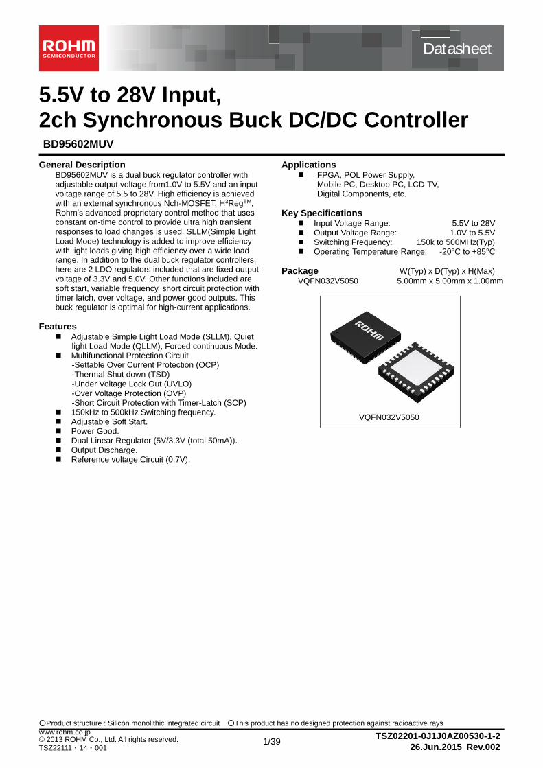
5.5V to 28V Input, 2ch Synchronous Buck DC/DC Controller BD95602MUV
General Description BD95602MUV is a dual buck regulator controller with adjustable output voltage from1.0V to 5.5V and an input voltage range of 5.5 to 28V. High efficiency is achieved with an external synchronous Nch-MOSFET. H3RegTM, Rohm’s advanced proprietary control method that uses constant on-time control to provide ultra high transient responses to load changes is used. SLLM(Simple Light Load Mode) technology is added to improve efficiency with light loads giving high efficiency over a wide load range. In addition to the dual buck regulator controllers, here are 2 LDO regulators included that are fixed output voltage of 3.3V and 5.0V. Other functions included are soft start, variable frequency, short circuit protection with timer latch, over voltage, and power good outputs. This buck regulator is optimal for high-current applications.
Features
Adjustable Simple Light Load Mode (SLLM), Quiet light Load Mode (QLLM), Forced continuous Mode.
Multifunctional Protection Circuit -Settable Over Current Protection (OCP) -Thermal Shut down (TSD) -Under Voltage Lock Out (UVLO) -Over Voltage Protection (OVP) -Short Circuit Protection with Timer-Latch (SCP)
150kHz to 500kHz Switching frequency. Adjustable Soft Start. Power Good. Dual Linear Regulator (5V/3.3V (total 50mA)). Output Discharge. Reference voltage Circuit (0.7V).
Applications FPGA, POL Power Supply,
Mobile PC, Desktop PC, LCD-TV, Digital Components, etc.
Key Specifications Input Voltage Range: 5.5V to 28V Output Voltage Range: 1.0V to 5.5V Switching Frequency: 150k to 500MHz(Typ) Operating Temperature Range: -20°C to +85°C
Package W(Typ) x D(Typ) x H(Max) VQFN032V5050 5.00mm x 5.00mm x 1.00mm
VQFN032V5050
Datasheet

2/39
TSZ02201-0J1J0AZ00530-1-2
© 2013 ROHM Co., Ltd. All rights reserved. 26.Jun.2015 Rev.002
www.rohm.co.jp
TSZ22111・15・001
BD95602MUV
Typical Application Circuit
4
5
3
2
1
910
21
20
19
18
17
1112131415
PGOOD1
EN1
BOOT1
HG1
SW1
PGOOD2
EN2
BOOT2
HG2
SW2
RE
G2
RE
G1
VIN
LG
2
PG
ND
2
AG
ND
RE
F
FB
2
FS
2
CT
L
2.5V
EN_3.3BD95602MUV
GND PGND
U1
3.3V
7
8
6
16
24
23
22
31302928272625 32
ILIM2
VO2
SS2
MC
TL2
FS
1
FB
1
ILIM1
MCTL1
SS1
PG
ND
1
LG
1
VO
1
L1
C9
C7
Q1
Q2
C5
R5
C3
C2
C1
C8
L2
C12
Q3
Q4
C6
R6
R7
C4 R8
R16
R26
R15 R25
C19
C29
EN_2.5
RE
G2_3.3
V
RE
G1_5V
+12V
Figure 1. Application Circuit
Pin Configuration
Figure 2. Pin Configuration
U1 BD95602MUV
3 1 2 4 5 6 7 8
9
10
11
12
13
14
15
16
24 23 22 21 20 19 18 17
32
31
30
29
28
27
26
25 PGND1
LG1
SW
2
HG
2
BO
OT
2
PG
OO
D2
SS
2
Vo2
ILIM
2
SW
1
HG
1
BO
OT
1
PG
OO
D1
SS
1
MC
TL1
REF
MCTL2
FS1
FB1
AGND
ILIM
1
FB2
FS2
CTL
REG2
REG1
VIN
LG2
PGND2
FIN
Vo1
EN
1
EN
2

3/39
TSZ02201-0J1J0AZ00530-1-2
© 2013 ROHM Co., Ltd. All rights reserved. 26.Jun.2015 Rev.002
www.rohm.co.jp
TSZ22111・15・001
BD95602MUV
Pin Descriptions
Pin No. Pin Name Function
1 24
SW2 SW1
Ground pin for High-side FET. The maximum voltage range of this pin is 30V.
2 23
HG2 HG1
High-side FET gate drive pin.
3 22
BOOT2 BOOT1
This is the power supply pin for High-side FET driver. The maximum voltage range to ground is to 35V, to SW pin is to 7V. In switching operations, the voltage swings from (VIN+REG1) to REG1 by BOOT pin operation.
4 21
EN2 EN1
When EN pin voltage is at least 2.3V, the status of the switching regulator becomes active. Conversely, the status switches off when EN pin voltage goes lower than 0.8V. This pin is pulled down to AGND with 1MΩ resistor.
5 20
PGOOD2 PGOOD1
If FB pin voltage is 15% or less of reference voltage, it will output low level. The output format is open drain, so please connect pull-up resistance.
6 19
SS2 SS1
This is the setting pin for soft start. The rising time is determined by the capacitor connected between SS and ground, and the fixed current inside IC after it is the status of low in standby mode. It controls the output voltage till SS voltage catch up the REF pin to become the SS terminal voltage.
7 27
VO2 VO1
This is the output discharge pin, and output voltage feedback pin for frequency setting.
8 17
ILIM2 ILIM1
This is the coil current limit setting pin. Set the resistor which is connected in between ground.
9 CTL
When CTL pin voltage is at least 2.3V, the status of the linear regulator REG1 and REG2 output becomes active. Conversely, the status switches off when CTL pin voltage goes lower than 0.8V. The switching regulator doesn’t become active when the status of CTL pin is low, if the status of EN pin is high. This pin is pulled up to VIN with 1MΩ resistor.
10 15
FS2 FS1
Frequency input. A resistor to ground will set the switching frequency. Frequencies from 150kHz to 500kHz are possible.
11 14
FB2 FB1
This is the output voltage feedback pin. The IC controls reference voltage and FB terminal voltage are almost same.
12 REF This is the output voltage setting pin. The IC controls reference voltage and FB terminal voltage are almost same.
13 AGND Ground input for control circuit.
16 18
MCTL2 MCTL1
This is the operation mode setting pin. If terminal voltage reaches less than 0.8V, it will be Low Level. If terminal voltage reaches more than 2.3V, it will be High Level. This pin is pulled down to AGND with 300kΩ resistor.
Input Control Mode
MCTL1 MCTL2
Low Low SLLM
Low High QLLM
High Low Continuous PWM Mode
High High Continuous PWM Mode
25 32
PGND1 PGND2
This is the ground pin for Low-side FET drive.
26 31
LG1 LG2
This is the Low-side FET gate drive pin. It is operated in switching between REG1 to PGND. ON resistance of output stage when High, it is 2Ω and when Low, it is 0.5Ω drive Low-side FET gate with the high pace.
28 REG2 This is the output pin for 3.3V/50mA linear regulator (5V/3.3V (total 50mA)). Please connect 10µF capacitor which characteristic is more than X5R near the pin.
29 REG1 This is the output pin for 5V/50mA linear regulator (5V/3.3V (total 50mA)). Please connect 10µF capacitor which characteristic is more than X5R near the pin.
30 VIN
Supply pin of H3RegTM control circuit and linear regulator. Monitor input voltage and determine necessary on-time. As a result, this terminal voltage changes, and then the IC operation become unstable. Please connect 10µF capacitor which characteristic is more than X5R near the pin.
FIN FIN This is the thermal PAD. Please connect to the ground.
4/39
TSZ02201-0J1J0AZ00530-1-2
© 2013 ROHM Co., Ltd. All rights reserved. 26.Jun.2015 Rev.002
www.rohm.co.jp
TSZ22111・15・001
BD95602MUV
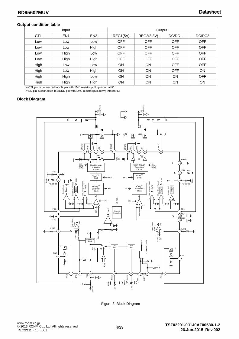
Output condition table
Input Output
CTL EN1 EN2 REG1(5V) REG2(3.3V) DC/DC1 DC/DC2
Low Low Low OFF OFF OFF OFF
Low Low High OFF OFF OFF OFF
Low High Low OFF OFF OFF OFF
Low High High OFF OFF OFF OFF
High Low Low ON ON OFF OFF
High Low High ON ON OFF ON
High High Low ON ON ON OFF
High High High ON ON ON ON
* CTL pin is connected to VIN pin with 1MΩ resistor(pull up) internal IC.
* EN pin is connected to AGND pin with 1MΩ resistor(pull down) internal IC.
Block Diagram
Figure 3. Block Diagram
3 2 1
31 32 22 23 24 26 25
11
6
8
Short through Protection
Circuit
SLLMTM
Block
H
3Reg
TM
Controller Block
Tim
er
Tim
er
14
12
17
21
Short through Protection
Circuit
SLLMTM
Block
H
3Reg
TM
Controller Block
4
30 29 18
Reference Block
5V Reg
Thermal Protection
EN1
REF
FB1
10 15
13
RFS1 FS1
AGND P
GN
D1
LG
1
SW
1
HG
1
BO
OT
1
PG
ND
2
LG
2
SW
2
HG
2
BO
OT
2
VIN
VIN
Vo
2
Adju
sta
ble
Vo
1
Adju
sta
ble
RE
G1
RE
G1
REG1 REG1
CL1 SCP1 OVP1
CL2 SCP2 OVP2
MCTL
FS2
MCTL
FS1
EN1 EN2
Short
Circuit P
rote
ct S
CP
2
RE
F
Short
Circuit P
rote
ct SC
P1
C
L1
Over
Curr
ent
Pro
tect
CL2
Over
Curr
ent
Pro
tect
TS
D
RE
G1
Pow
er
Good
MC
TL
SLL
M M
ode C
ontr
ol
RE
G1
5V
RE
G1
MC
TL
1
VIN
VIN
5.5~
28V
SS2
FB2
FS2
EN2
PGOOD1
19 SS1
Over
Vo
ltag
e P
rote
ct
OV
P2
Over
Vo
ltag
e P
rote
ct
OV
P1
RE
F
9
28
RE
G2
3.3
V
CT
L
20 R
EG
1
5 R
EG
1
Pow
er
Good
7
Vo
2
RE
G2
PGOOD2
3.3V Reg
Vo
1
Tim
er
Tim
er
UV
LO
PG
ND
2
PG
ND
1
27
Vo
1
RE
F
ILIM1 ILIM2
SW
2
SW
1
16
MC
TL
2
5/39
TSZ02201-0J1J0AZ00530-1-2
© 2013 ROHM Co., Ltd. All rights reserved. 26.Jun.2015 Rev.002
www.rohm.co.jp
TSZ22111・15・001
BD95602MUV
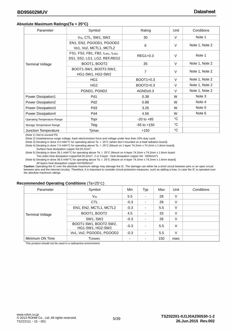
Absolute Maximum Ratings(Ta = 25°C)
Parameter Symbol Rating Unit Conditions
Terminal Voltage
VIN, CTL, SW1, SW2 30 V Note 1
EN1, EN2, PGOOD1, PGOOD2
Vo1, Vo2, MCTL1, MCTL2 6 V Note 1, Note 2
FS1, FS2, FB1, FB2, ILIM1, ILIM2,
SS1, SS2, LG1, LG2, REF,REG2 REG1+0.3 V Note 1
BOOT1, BOOT2 35 V Note 1, Note 2
BOOT1-SW1, BOOT2-SW2,
HG1-SW1, HG2-SW2 7 V Note 1, Note 2
HG1 BOOT1+0.3 V Note 1, Note 2
HG2 BOOT2+0.3 V Note 1, Note 2
PGND1, PGND2 AGND±0.3 V Note 1, Note 2
Power Dissipation1 Pd1 0.38 W Note 3
Power Dissipation2 Pd2 0.88 W Note 4
Power Dissipation3 Pd3 3.26 W Note 5
Power Dissipation4 Pd4 4.56 W Note 6
Operating Temperature Range Topr -20 to +85 °C
Storage Temperature Range Tstg -55 to +150 °C
Junction Temperature Tjmax +150 °C
(Note 1) Not to exceed Pd.
(Note 2) Instantaneous surge voltage, back electromotive force and voltage under less than 10% duty cycle.
(Note 3) Derating in done 3.0 mW/°C for operating above Ta ≥ 25°C (when don’t mounted on a heat radiation board).
(Note 4) Derating in done 7.0 mW/°C for operating above Ta ≥ 25°C (Mount on 1-layer 74.2mm x 74.2mm x 1.6mm board).
Surface heat dissipation copper foil:20.2mm2.
(Note 5) Derating in done 26.1 mW/°C for operating above Ta ≥ 25°C (Mount on 4-layer 74.2mm x 74.2mm x 1.6mm board
Two sides heat dissipation copperfoil:20.2mm2. 2 or 3-layer : heat dissipation copper foil : 5505mm2).
(Note 6) Derating in done 36.5 mW/°C for operating above Ta ≥ 25°C (Mount on 4-layer 74.2mm x 74.2mm x 1.6mm board)
All layers heat dissipation copper foil:5505mm2.
Caution: Operating the IC over the absolute maximum ratings may damage the IC. The damage can either be a short circuit between pins or an open circuit between pins and the internal circuitry. Therefore, it is important to consider circuit protection measures, such as adding a fuse, in case the IC is operated over the absolute maximum ratings.
Recommended Operating Conditions (Ta=25°C)
Parameter Symbol Min Typ Max Unit Conditions
Terminal Voltage
VIN 5.5 - 28 V
CTL -0.3 - 28 V
EN1, EN2, MCTL1, MCTL2 -0.3 - 5.5 V
BOOT1, BOOT2 4.5 - 33 V
SW1, SW2 -0.3 - 28 V
BOOT1-SW1, BOOT2-SW2, HG1-SW1, HG2-SW2
-0.3 - 5.5 V
Vo1, Vo2, PGOOD1, PGOOD2 -0.3 - 5.5 V
Minimum ON Time TONMIN - - 150 nsec
This product should not be used in a radioactive environment.

6/39
TSZ02201-0J1J0AZ00530-1-2
© 2013 ROHM Co., Ltd. All rights reserved. 26.Jun.2015 Rev.002
www.rohm.co.jp
TSZ22111・15・001
BD95602MUV
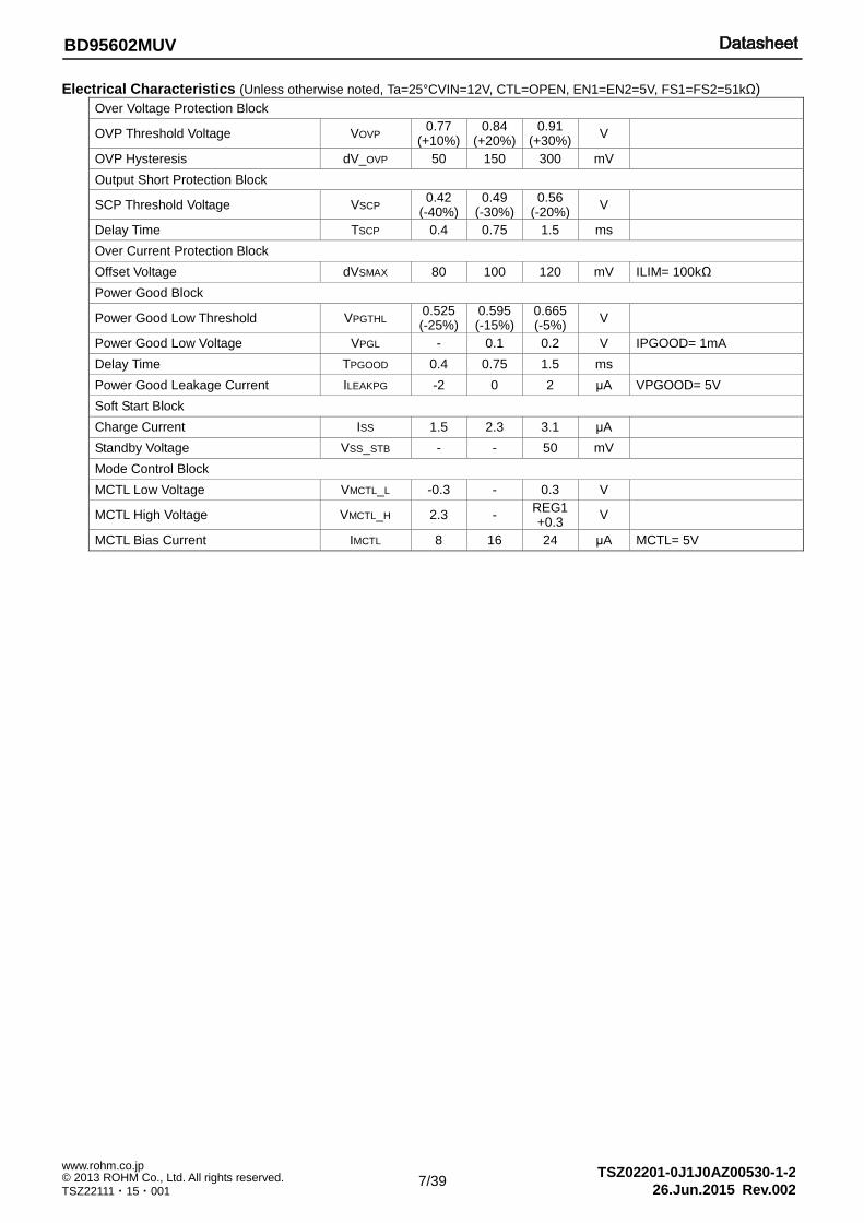
Electrical Characteristics (Unless otherwise noted, Ta=25°CVIN=12V, CTL=OPEN, EN1=EN2=5V, FS1=FS2=51kΩ)
Parameter Symbol Min Typ Max Unit Conditions
VIN Standby Current ISTB 70 150 250 μA EN1= EN2= 0V, CTL= 5V
VIN Bias Current IIN 60 130 230 μA Vo1= 5V
VIN Shut Down Mode Current ISHD 6 12 18 μA CTL= 0V
CTL Low Voltage VCTLL -0.3 - 0.8 V
CTL High Voltage VCTLH 2.3 - 28 V
CTL Bias Current ICTL -18 -12 -6 μA CTL= 0V
EN Low Voltage VENL -0.3 - 0.8 V
EN High Voltage VENH 2.3 - 5.5 V
EN Bias Current IEN - 3 6 μA EN= 3V
5V Linear Regulator -VIN
REG1 Output Voltage VREG1 4.90 5.00 5.10 V IREG1=1mA
Maximum Current IREG1 50 - - mA IREG2= 0mA, (Note 7)
Line Regulation REG.I1 - 90 180 mV VIN= 5.5 to 28V
Load Regulation REG.L1 - 30 50 mV IREG1= 0 to 30mA
3.3V Linear Regulator
REG2 Output Voltage VREG2 3.27 3.30 3.33 V IREG2= 1mA
Maximum Current IREG2 50 - - mA IREG1= 0mA, (Note 7)
Line Regulation REG.I2 - - 20 mV VIN= 5.5 to 28V
Load Regulation REG.L2 - - 30 mV IREG2= 0 to 30mA
5V Linear Regulator -Vo1
Input Threshold Voltage REG1th 4.1 4.4 4.7 V Vo1: Sweep up
Input Delay Time TREG1 1.5 3 6 ms
Switch Resistance RREG1 - 1.0 3.0 Ω
Under Voltage Lock Out Block
REG1 Threshold Voltage REG1_ UVLO 3.9 4.2 4.5 V REG1: Sweep up
Hysteresis Voltage dV_ UVLO 50 100 200 mV REG1: Sweep down
Output Voltage Sense Block
Feedback Voltage1 VFB1 0.693 0.700 0.707 V
FB1 Bias Current IFB1 - 0 1 μA FB1= REF
Output Discharge Resistance1 RDISOUT1 50 100 200 Ω
Feedback Voltage2 VFB2 0.693 0.700 0.707 V
FB2 Bias Current IFB2 - 0 1 μA FB2= REF
Output Discharge Resistance2 RDISOUT2 50 100 200 Ω
H3REGTM Control Block
On Time1 tON1 0.760 0.910 1.060 μs Vo1= 5V,FS1= 51kΩ
On Time2 tON2 0.470 0.620 0.770 μs Vo2= 3.3V ,FS2= 51kΩ
Maximum On Time 1 tONMAX1 2.5 5 10 μs Vo1= 5V
Maximum On Time 2 tONMAX2 1.65 3.3 6.6 μs Vo2= 3.3V
Minimum Off Time tOFFMIN - 0.2 0.4 μs
FET Driver Block
HG High Side ON Resistance HGHON - 3.0 6.0 Ω
HG Low Side ON Resistance HGLON - 2.0 4.0 Ω
LG High Side ON Resistance LGHON - 2.0 4.0 Ω
LG Low Side ON Resistance LGLON - 0.5 1.0 Ω
(Note 7) IREG1+IREG2 ≤ 50mA.
7/39
TSZ02201-0J1J0AZ00530-1-2
© 2013 ROHM Co., Ltd. All rights reserved. 26.Jun.2015 Rev.002
www.rohm.co.jp
TSZ22111・15・001
BD95602MUV
Electrical Characteristics (Unless otherwise noted, Ta=25°CVIN=12V, CTL=OPEN, EN1=EN2=5V, FS1=FS2=51kΩ)
Over Voltage Protection Block
OVP Threshold Voltage VOVP 0.77
(+10%) 0.84
(+20%) 0.91
(+30%) V
OVP Hysteresis dV_OVP 50 150 300 mV
Output Short Protection Block
SCP Threshold Voltage VSCP 0.42
(-40%) 0.49
(-30%) 0.56
(-20%) V
Delay Time TSCP 0.4 0.75 1.5 ms
Over Current Protection Block
Offset Voltage dVSMAX 80 100 120 mV ILIM= 100kΩ
Power Good Block
Power Good Low Threshold VPGTHL 0.525 (-25%)
0.595 (-15%)
0.665 (-5%)
V
Power Good Low Voltage VPGL - 0.1 0.2 V IPGOOD= 1mA
Delay Time TPGOOD 0.4 0.75 1.5 ms
Power Good Leakage Current ILEAKPG -2 0 2 μA VPGOOD= 5V
Soft Start Block
Charge Current ISS 1.5 2.3 3.1 μA
Standby Voltage VSS_STB - - 50 mV
Mode Control Block
MCTL Low Voltage VMCTL_L -0.3 - 0.3 V
MCTL High Voltage VMCTL_H 2.3 - REG1 +0.3
V
MCTL Bias Current IMCTL 8 16 24 μA MCTL= 5V

8/39
TSZ02201-0J1J0AZ00530-1-2
© 2013 ROHM Co., Ltd. All rights reserved. 26.Jun.2015 Rev.002
www.rohm.co.jp
TSZ22111・15・001
BD95602MUV
Typical Performance Curves (Reference data)
Figure 4. Switching Waveform (Vo= 5V, Io= 0A, PWM)
Figure 5. Switching Waveform (Vo= 5V, Io= 8A, PWM)
Figure 6. Switching Waveform (Vo= 5V, Io= 0A, QLLM)
Figure 7. Switching Waveform (Vo= 5V, Io= 0A, SLLM)
グラフ中の文字は 9pt
HG 10V/div
SW 10V/div
LG 5V/div
2μs
HG 10V/div
SW 10V/div
LG 5V/div
2μs
HG 10V/div
SW 10V/div
LG 5V/div
HG 10V/div
SW 10V/div
LG 5V/div
10μs 10μs

9/39
TSZ02201-0J1J0AZ00530-1-2
© 2013 ROHM Co., Ltd. All rights reserved. 26.Jun.2015 Rev.002
www.rohm.co.jp
TSZ22111・15・001
BD95602MUV
Typical Performance Curves - continued
Figure 8. Switching Waveform (Vo= 3.3V, Io= 0A, PWM)
Figure 9. Switching Waveform (Vo= 3.3V, Io= 8A, PWM)
Figure 10. Switching Waveform (Vo= 3.3V, Io= 0A, QLLM)
Figure 11. Switching Waveform (Vo= 3.3V, Io= 0A, SLLM)
HG 10V/div
SW 10V/div
LG 5V/div
2μs
HG 10V/div
SW 10V/div
LG 5V/div
2μs
HG 10V/div
SW 10V/div
LG 5V/div
HG 10V/div
SW 10V/div
LG 5V/div
10μs 10μs

10/39
TSZ02201-0J1J0AZ00530-1-2
© 2013 ROHM Co., Ltd. All rights reserved. 26.Jun.2015 Rev.002
www.rohm.co.jp
TSZ22111・15・001
BD95602MUV
Typical Performance Curves - continued
Figure 12. Switching Waveform (Vo= 1V, Io= 0A, PWM)
Figure 13. Switching Waveform (Vo= 1V, Io= 8A, PWM)
Figure 14. Switching Waveform (Vo= 1V, Io= 0A, QLLM)
Figure 15. Switching Waveform (Vo= 1V, Io= 0A, SLLM)
HG 10V/div
SW 10V/div
LG 5V/div
2μs
HG 10V/div
SW 10V/div
LG 5V/div
2μs
HG 10V/div
SW 10V/div
LG 5V/div
HG 10V/div
SW 10V/div
LG 5V/div
10μs 10μs

11/39
TSZ02201-0J1J0AZ00530-1-2
© 2013 ROHM Co., Ltd. All rights reserved. 26.Jun.2015 Rev.002
www.rohm.co.jp
TSZ22111・15・001
BD95602MUV
Typical Performance Curves - continued
0
20
40
60
80
100
1 10 100 1000 10000
Io[mA]
η[%
]
0
20
40
60
80
100
1 10 100 1000 10000
Io[mA]
η[%
]
0
20
40
60
80
100
1 10 100 1000 10000
Io[mA]
η[%
]
Figure 16. Efficiency (Vo= 5V, PWM)
Figure 17. Efficiency (Vo= 5V, QLLM)
Figure 18. Efficiency
(Vo= 5V, SLLM)
Figure 19. Efficiency
(Vo= 3.3V, PWM)
7V 12V
21V
7V 12V
21V
7V
12V
21V
5V
0
20
40
60
80
100
1 10 100 1000 10000
Io[mA]
η[%
]
7V
12V
21V

12/39
TSZ02201-0J1J0AZ00530-1-2
© 2013 ROHM Co., Ltd. All rights reserved. 26.Jun.2015 Rev.002
www.rohm.co.jp
TSZ22111・15・001
BD95602MUV
Typical Performance Curves - continued
0
20
40
60
80
100
1 10 100 1000 10000
η[%
]
Io[mA]
0
20
40
60
80
100
1 10 100 1000 10000
η[%
]
Io[mA]
0
20
40
60
80
100
1 10 100 1000 10000η
[%]
Io[mA]
0
20
40
60
80
100
1 10 100 1000 10000
η[%
]
Io[mA]
Figure 20. Efficiency (Vo= 3.3V, QLLM)
Figure 22. Efficiency (Vo= 1V, PWM)
Figure 23. Efficiency (Vo= 1V, QLLM)
7V 12V
21V
7V
12V
21V
7V 12V
21V
Figure 21. Efficiency (Vo= 3.3V, SLLM)
7V 12V
21V
13/39
TSZ02201-0J1J0AZ00530-1-2
© 2013 ROHM Co., Ltd. All rights reserved. 26.Jun.2015 Rev.002
www.rohm.co.jp
TSZ22111・15・001
BD95602MUV
Typical Performance Curves - continued
0
20
40
60
80
100
1 10 100 1000 10000
η[%
]
Io[mA]
Figure 24. Efficiency (Vo= 1V, SLLM)
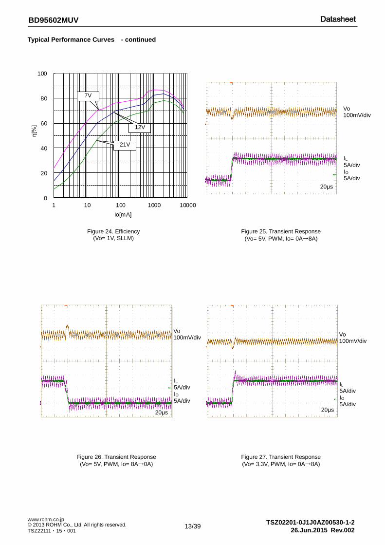
Figure 26. Transient Response
(Vo= 5V, PWM, Io= 8A→0A)
Figure 27. Transient Response
(Vo= 3.3V, PWM, Io= 0A→8A)
12V
21V
7V
Figure 25. Transient Response
(Vo= 5V, PWM, Io= 0A→8A)
20μs
Vo 100mV/div
IL 5A/div IO 5A/div
20μs
Vo 100mV/div
IL 5A/div IO 5A/div
20μs
Vo 100mV/div
IL 5A/div IO 5A/div

14/39
TSZ02201-0J1J0AZ00530-1-2
© 2013 ROHM Co., Ltd. All rights reserved. 26.Jun.2015 Rev.002
www.rohm.co.jp
TSZ22111・15・001
BD95602MUV
Typical Performance Curves - continued
Figure 28. Transient Response
(Vo= 3.3V, PWM, Io= 8A→0A)
Figure 29. Transient Response
(Vo= 1V, PWM, Io= 0A→8A)
Figure 30. Transient Response
(Vo= 1V, PWM, Io= 8A→0A)
Figure 31. Output Voltage (Vo= 5V, PWM, Io= 0A)
20μs
Vo 100mV/div
IL 5A/div IO 5A/div
20μs
Vo 100mV/div
IL 5A/div IO 5A/div
20μs
Vo 100mV/div
IL 5A/div IO 5A/div
2μs
Vo 50mV/div

15/39
TSZ02201-0J1J0AZ00530-1-2
© 2013 ROHM Co., Ltd. All rights reserved. 26.Jun.2015 Rev.002
www.rohm.co.jp
TSZ22111・15・001
BD95602MUV
Typical Performance Curves - continued
Figure 32. Output Voltage (Vo= 5V, PWM, Io= 8A)
Figure 33. Output Voltage (Vo= 5V, QLLM, Io= 0A)
Figure 34. Output Voltage (Vo= 5V, SLLM, Io= 0A)
Figure 35. Output Voltage (Vo= 3.3V, PWM, Io= 0A)
2μs
Vo 50mV/div
Vo 50mV/div
Vo 50mV/div
Vo 50mV/div
2μs 2μs
10μs 2μs
16/39
TSZ02201-0J1J0AZ00530-1-2
© 2013 ROHM Co., Ltd. All rights reserved. 26.Jun.2015 Rev.002
www.rohm.co.jp
TSZ22111・15・001
BD95602MUV
Typical Performance Curves - continued
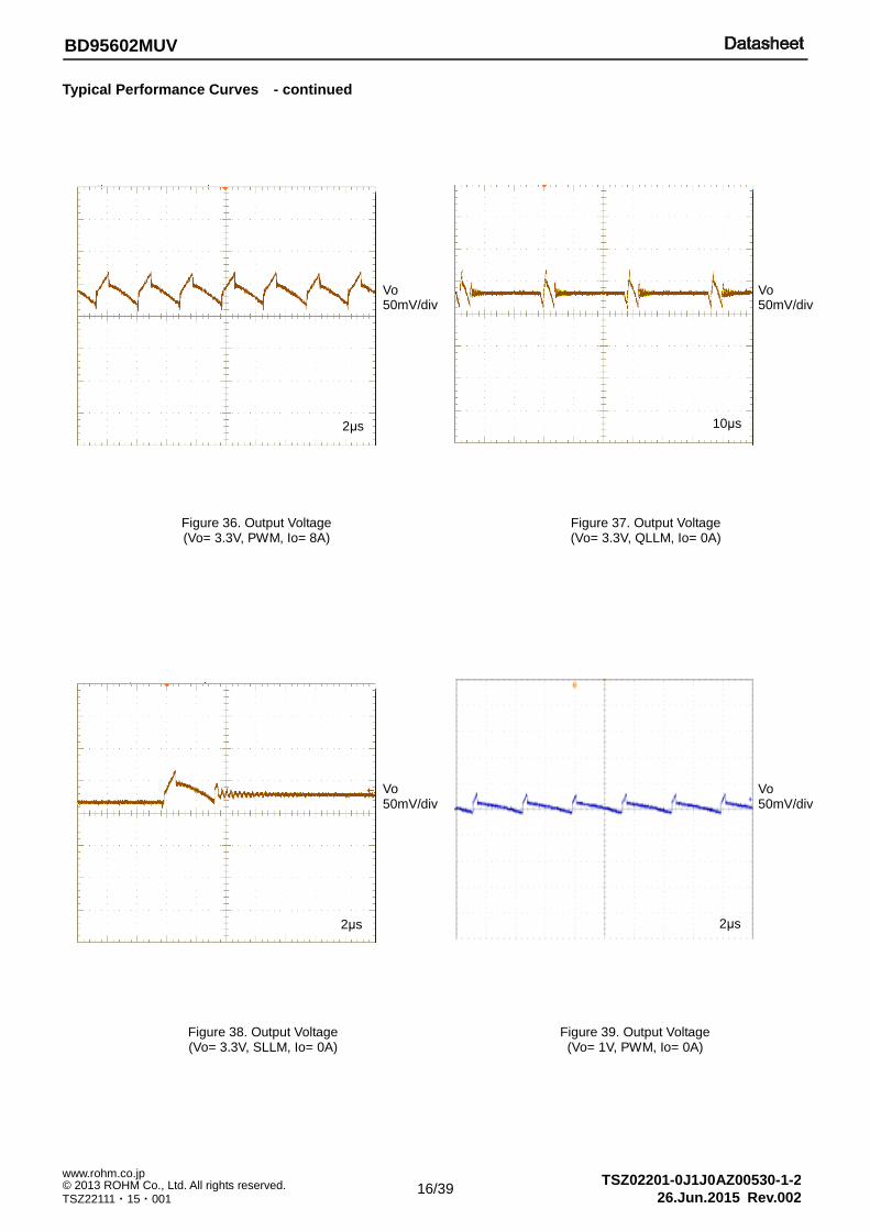
Figure 36. Output Voltage (Vo= 3.3V, PWM, Io= 8A)
Figure 37. Output Voltage (Vo= 3.3V, QLLM, Io= 0A)
Figure 38. Output Voltage (Vo= 3.3V, SLLM, Io= 0A)
Figure 39. Output Voltage (Vo= 1V, PWM, Io= 0A)
2μs
Vo 50mV/div
Vo 50mV/div
Vo 50mV/div
Vo 50mV/div
2μs
10μs 2μs
17/39
TSZ02201-0J1J0AZ00530-1-2
© 2013 ROHM Co., Ltd. All rights reserved. 26.Jun.2015 Rev.002
www.rohm.co.jp
TSZ22111・15・001
BD95602MUV
Typical Performance Curves - continued
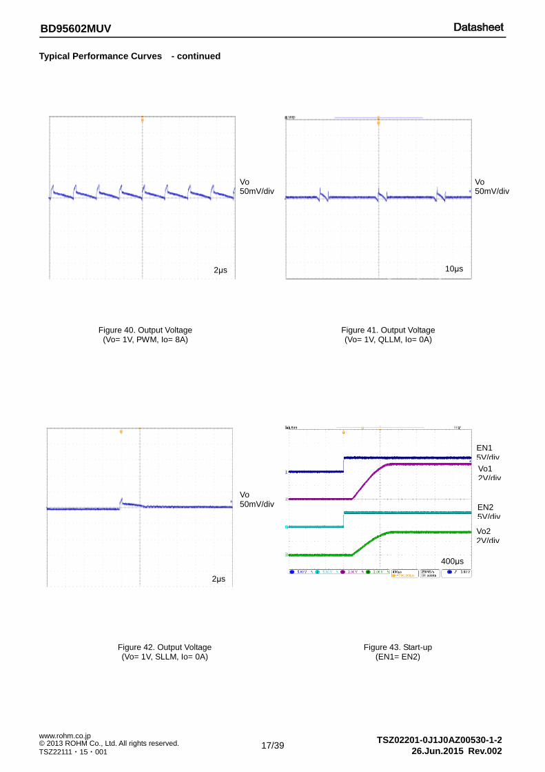
Figure 40. Output Voltage (Vo= 1V, PWM, Io= 8A)
Figure 41. Output Voltage (Vo= 1V, QLLM, Io= 0A)
Figure 42. Output Voltage (Vo= 1V, SLLM, Io= 0A)
Figure 43. Start-up (EN1= EN2)
Vo 50mV/div
Vo 50mV/div
Vo 50mV/div
2μs
10μs 2μs
EN1 5V/div
Vo1 2V/div
EN2 5V/div
Vo2 2V/div
400μs

18/39
TSZ02201-0J1J0AZ00530-1-2
© 2013 ROHM Co., Ltd. All rights reserved. 26.Jun.2015 Rev.002
www.rohm.co.jp
TSZ22111・15・001
BD95602MUV
Typical Performance Curves - continued
IOUT-frequency (VOUT=5V, R(FS)=68kΩ )
300
350
400
450
500
0 1 2 3 4 5 6 7
IOUT [A]
frequency [
kH
z]
VIN=7.5VVIN=12V
VIN=18V
Figure 44. Start-up
(EN2→EN1)
Figure 45. Start-up
(EN1→EN2)
Figure 46. Start-up
(EN1/2→PGOOD1/2)
Figure 47. Io-frequency (Vo= 5V, PWM, RFS= 68kΩ)
40ms
EN1 5V/div
Vo1 2V/div
EN2 5V/div
Vo2 2V/div
EN1 5V/div
Vo1 2V/div
EN2 5V/div
Vo2 2V/div
40ms
40ms
EN1 5V/div
PGOOD1 2V/div
EN2 5V/div
PGOOD2 2V/div

19/39
TSZ02201-0J1J0AZ00530-1-2
© 2013 ROHM Co., Ltd. All rights reserved. 26.Jun.2015 Rev.002
www.rohm.co.jp
TSZ22111・15・001
BD95602MUV
Typical Performance Curves - continued
IOUT-frequency (VOUT=5V, R(FS)=68kΩ )
300
350
400
450
500
0 1 2 3 4 5 6 7
IOUT [A]
frequency [
kH
z]
VIN=7.5VVIN=12V
VIN=18V
0
0.5
1
1.5
2
2.5
0 50 100 150
RFS [kΩ ]O
NTIM
E [
usec]
VOUT=5V
VOUT=3.3V
0
100
200
300
400
500
600
700
0 50 100 150
RFS [kΩ ]
frequency [
kH
z]
VOUT=5V
VOUT=3.3V
0.000
0.500
1.000
1.500
2.000
2.500
3.000
3.500
4.000
4.500
5.000
5.500
0 2 4 6 8 10 12 14 16
IOUT [A]
VO
UT [
V]
VIN=7.5V(-5)
VIN=21V(-5)
VIN=7.5V(75)
VIN=21V(75)
Figure 48. lo-frequency (Vo= 3.3V, PWM, RFS= 68kΩ)
Figure 49. On time-RFS
Figure 50. SW Frequency-RFS Figure 51. Current Limit (Vo= 5V)
20/39
TSZ02201-0J1J0AZ00530-1-2
© 2013 ROHM Co., Ltd. All rights reserved. 26.Jun.2015 Rev.002
www.rohm.co.jp
TSZ22111・15・001
BD95602MUV
Typical Performance Curves - continued
IOUT - REG2 voltage
2.8
2.9
3
3.1
3.2
3.3
3.4
0 50 100 150 200 250
IOUT [mA]
REG
2 v
oltage [
V]
IOUT - REG1 voltage
4.5
4.6
4.7
4.8
4.9
5
5.1
0 50 100 150 200 250
IOUT [mA]R
EG
1 v
oltage [
V]
0.000
0.500
1.000
1.500
2.000
2.500
3.000
3.500
0 2 4 6 8 10 12 14 16
IOUT [A]
VO
UT [
V]
VIN=7.5V(-5)
VIN=21V(-5)
VIN=7.5V(75)
VIN=21V(75)
Figure 52. Current Limit (Vo= 3.3V)
Figure 53. REG1 Load Regulation
Figure 54. REG2 Load Regulation
21/39
TSZ02201-0J1J0AZ00530-1-2
© 2013 ROHM Co., Ltd. All rights reserved. 26.Jun.2015 Rev.002
www.rohm.co.jp
TSZ22111・15・001
BD95602MUV
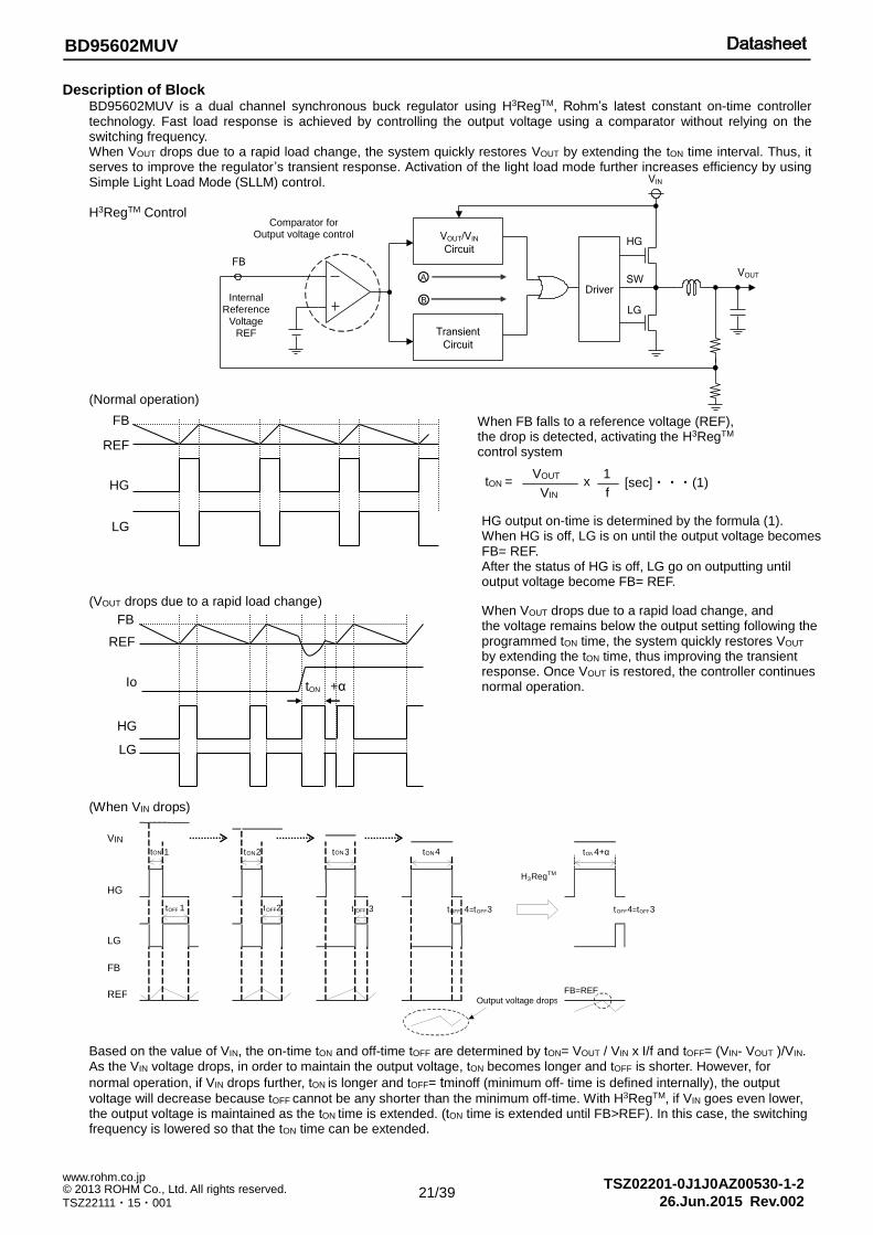
Description of Block BD95602MUV is a dual channel synchronous buck regulator using H3RegTM, Rohm’s latest constant on-time controller technology. Fast load response is achieved by controlling the output voltage using a comparator without relying on the switching frequency. When VOUT drops due to a rapid load change, the system quickly restores VOUT by extending the tON time interval. Thus, it serves to improve the regulator’s transient response. Activation of the light load mode further increases efficiency by using Simple Light Load Mode (SLLM) control. H3RegTM Control
(Normal operation)
(VOUT drops due to a rapid load change)
(When VIN drops)
Based on the value of VIN, the on-time tON and off-time tOFF are determined by tON= VOUT / VIN x I/f and tOFF= (VIN- VOUT )/VIN. As the VIN voltage drops, in order to maintain the output voltage, tON becomes longer and tOFF is shorter. However, for
normal operation, if VIN drops further, tON is longer and tOFF= tminoff (minimum off- time is defined internally), the output
voltage will decrease because tOFF cannot be any shorter than the minimum off-time. With H3RegTM, if VIN goes even lower, the output voltage is maintained as the tON time is extended. (tON time is extended until FB>REF). In this case, the switching frequency is lowered so that the tON time can be extended.
B
A
Comparator for
Output voltage control
Internal Reference
Voltage REF
FB
VOUT/VIN
Circuit
Transient
Circuit
Driver
HG
SW
LG
VIN
VOUT
FB
REF
HG
LG HG output on-time is determined by the formula (1). When HG is off, LG is on until the output voltage becomes FB= REF. After the status of HG is off, LG go on outputting until output voltage become FB= REF.
When FB falls to a reference voltage (REF), the drop is detected, activating the H3RegTM
control system
REF
FB
HG
Io
LG
tON +α
When VOUT drops due to a rapid load change, and the voltage remains below the output setting following the programmed tON time, the system quickly restores VOUT by extending the tON time, thus improving the transient response. Once VOUT is restored, the controller continues normal operation.
tON = VOUT
VIN x
1
f [sec]・・・(1)
HG
LG
FB
REF
VIN t ON 1 t ON 2 t ON 3 t ON 4
t OFF 1 t OFF 2 t OFF 3 t OFF 4 = t OFF 3
t ON 4+α
t OFF 4 = t OFF 3
H 3 Reg TM
FB=REF Output voltage drops

22/39
TSZ02201-0J1J0AZ00530-1-2
© 2013 ROHM Co., Ltd. All rights reserved. 26.Jun.2015 Rev.002
www.rohm.co.jp
TSZ22111・15・001
BD95602MUV
Description of Block - continued Light Load Control (SLLM)
(QLLM)
MCTL1 MCTL2 Control Mode Start-up
L L SLLM PWM
L H QLLM PWM
H X PWM PWM
FB
REF
HG
LG
0A
FB
REF
HG
LG
0A
The BD95602MUV operates in PWM mode until the SS
input reaches the clamp voltage (2.5V), regardless of the
control mode setting, this assures stable operation while the
during soft start.
Load COUT
SLLM will activate when the LG pin is off and the coil current is near 0A (current flows from VOUT to SW). When the FB input is lower than the REF voltage again, HG will be enabled once again.
QLLM will activate when the LG pin is off and the coil current is near 0A (current flows from VOUT to SW). In this case, the next HG is prevented. Then, when FB falls below the output programmed voltage within the programmed time (Typ= 40μs), HG will resume. In the case where FB doesn’t fall in the programmed time, LG is forced on causing VOUT to fall. As a result, the next HG is on.
*Attention: To effect the rapid transient response, the H3RegTM control monitors the current from the output capacitor to the load using the ESR of the output capacitor Do not use ceramic capacitors on COUT side of power supply. Ceramic bypass capacitors can be used near the individual loads if desired.
23/39
TSZ02201-0J1J0AZ00530-1-2
© 2013 ROHM Co., Ltd. All rights reserved. 26.Jun.2015 Rev.002
www.rohm.co.jp
TSZ22111・15・001
BD95602MUV
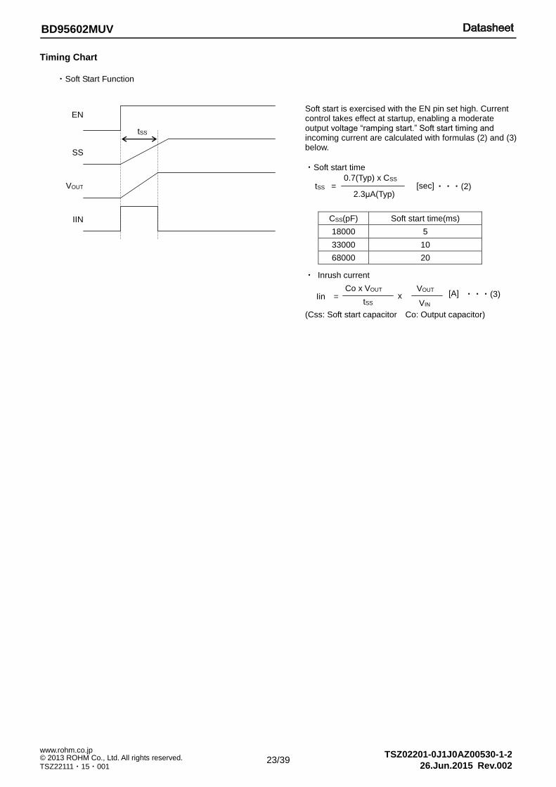
Timing Chart
・Soft Start Function
Soft start is exercised with the EN pin set high. Current control takes effect at startup, enabling a moderate output voltage “ramping start.” Soft start timing and incoming current are calculated with formulas (2) and (3) below.
・Soft start time
・ Inrush current
(Css: Soft start capacitor Co: Output capacitor)
CSS(pF) Soft start time(ms)
18000 5
33000 10
68000 20
EN
SS
VOUT
IIN
tSS
tSS = 0.7(Typ) x CSS
2.3μA(Typ) [sec] ・・・(2)
Iin = Co x VOUT
tSS
[A] ・・・(3) x VOUT
VIN

24/39
TSZ02201-0J1J0AZ00530-1-2
© 2013 ROHM Co., Ltd. All rights reserved. 26.Jun.2015 Rev.002
www.rohm.co.jp
TSZ22111・15・001
BD95602MUV
Timing Chart - continued
・Notes when waking up with CTL pin or VIN pin
If EN pin is high or short (or pull up resistor) to REG1 pin, IC starts up by switching CTL pin, the IC might fail to start up (SCP function) with the reason below, please be careful of SS pin and REF pin capacitor capacity.
CTL
(Vin)
EN
REG1(5V)
REG2(3.3V)
SCP_REF
SS
REFFB
FB
FB
FBabout 1.5V
SCP becomes valid from
the point SS reached 1.5V.
SCP invalid for
SS has not reached 1.5V.
SCP is valid here,
because this is
SCP valid area
and also because
FB fall below
SCP_REF.
SCP will be
effective with
EN=ON at this
section.
SW
Start up NG
EN
SW
Start up OK
SCP valid area
SCP is valid here,but with FB exceeding
SCP_REF it is normally activate-able
area.
SCP is effective at SCP_REF>FB condition.
SCP
SCP protection (function) activates when output
shorts and FB falls below the activation standard
of SCP.
Inclination of REF is
influenced by the external
condenserconnected to
REF.
? To be accurate,Delay occurs after SCP activating.
But this shows the relationship of each signals briefly.
Inner Reference
Circuit
Delay SCP
PWM (Switching control signal)
1ms(Typ)
SCP circuit
BG
SCP_REF
SCP
CTL
REF
SS
REG1 REG2 FB
VIN

25/39
TSZ02201-0J1J0AZ00530-1-2
© 2013 ROHM Co., Ltd. All rights reserved. 26.Jun.2015 Rev.002
www.rohm.co.jp
TSZ22111・15・001
BD95602MUV
Output Discharge
・Timer Latch Type Output Short Circuit Protection
・Over Voltage Protection
It will be available to use if connecting VOUT pin to DC/DC output. (about 100Ω) . Discharge function operates when <1> EN=’L’ <2> UVLO= ON(If input voltage is low) <3> SCP latch <4> TSD= ON. The function at output discharge time is shown as left.
[1] When switch to low from high with EN pin.
If EN pin voltage is below than EN threshold voltage, output discharge function is operated, and discharge output capacitor charge.
[2] When switch to low from high with EN pin
1) IC is in normal operation until REG1 voltage becomes lower than
UVLO voltage. However, because VIN voltage also becomes low, output
voltage will drop, too.
2) If REG1 voltage reaches the UVLO voltage, output discharge function is
operated, and discharge output capacitor charge.
3) In addition, if REG1 voltage drops, inner IC logic cannot operate, so that
output discharge function does not work, and becomes output Hi-z.
(In case, FB has resistor against ground, discharge at the resistor. )
VIN,CTL
EN
VOUT
Short protection is enabled when the output voltage falls to or below REF X 0.7. Once the programmed time period has elapsed, the output is latched off to prevent destruction of the circuit. (HG= Low, LG= Low) Output voltage can be restored either by cycling the EN pin or disabling UVLO.
FB
HG
LG
REF x 1.2
Switching
When the output voltage increases to or above REF x 1.2(Typ), output over voltage protection is enabled, and the Low-side FET turns on to reduce the output. (LG= High, HG= Low). When the output falls to within normal operation, the function is restored to normal operation.
FB
SCP
EN / UVLO
REF x 0.7
0.75ms(Typ)
The efficiency of VIN voltage drop output discharge
VIN, CTL REG1
VOUT
Output discharge
Output Hi-Z
UVLO ON

26/39
TSZ02201-0J1J0AZ00530-1-2
© 2013 ROHM Co., Ltd. All rights reserved. 26.Jun.2015 Rev.002
www.rohm.co.jp
TSZ22111・15・001
BD95602MUV
・Over current protection circuit
During normal operation, if FB is less than REF, HG is
high during the time tON, but when the coil current
exceeds the ILIMIT threshold, HG is set to off. The next
pulse returns to normal operation if the output voltage
drops after the maximum on-time or IL becomes lower
than ILIMIT.
tON tON
HG
LG
IL
tON tON
tOFF1 tOFF1 tOFF1 tOFFα
OCP detection
Over current protection setting value
27/39
TSZ02201-0J1J0AZ00530-1-2
© 2013 ROHM Co., Ltd. All rights reserved. 26.Jun.2015 Rev.002
www.rohm.co.jp
TSZ22111・15・001
BD95602MUV
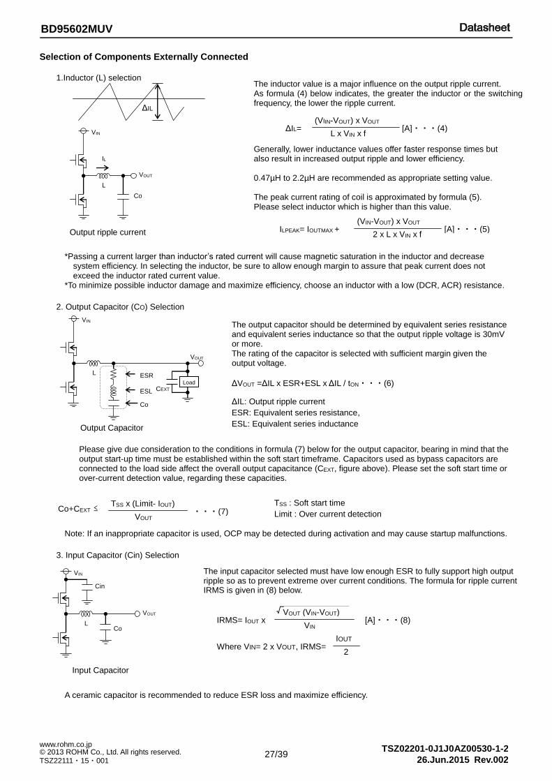
Selection of Components Externally Connected
1.Inductor (L) selection
*Passing a current larger than inductor’s rated current will cause magnetic saturation in the inductor and decrease system efficiency. In selecting the inductor, be sure to allow enough margin to assure that peak current does not exceed the inductor rated current value.
*To minimize possible inductor damage and maximize efficiency, choose an inductor with a low (DCR, ACR) resistance.
2. Output Capacitor (CO) Selection
Please give due consideration to the conditions in formula (7) below for the output capacitor, bearing in mind that the output start-up time must be established within the soft start timeframe. Capacitors used as bypass capacitors are connected to the load side affect the overall output capacitance (CEXT, figure above). Please set the soft start time or over-current detection value, regarding these capacities.
Note: If an inappropriate capacitor is used, OCP may be detected during activation and may cause startup malfunctions.
3. Input Capacitor (Cin) Selection
A ceramic capacitor is recommended to reduce ESR loss and maximize efficiency.
The inductor value is a major influence on the output ripple current. As formula (4) below indicates, the greater the inductor or the switching frequency, the lower the ripple current.
ΔIL= (VIIN-VOUT) x VOUT
L x VIN x f [A]・・・(4)
Generally, lower inductance values offer faster response times but also result in increased output ripple and lower efficiency. 0.47µH to 2.2µH are recommended as appropriate setting value. The peak current rating of coil is approximated by formula (5). Please select inductor which is higher than this value.
Input Capacitor
Output ripple current
The output capacitor should be determined by equivalent series resistance and equivalent series inductance so that the output ripple voltage is 30mV or more. The rating of the capacitor is selected with sufficient margin given the output voltage.
ΔVOUT =ΔIL x ESR+ESL x ΔIL / tON・・・(6)
Co+CEXT ≤ TSS x (Limit- IOUT)
VOUT ・・・(7)
TSS : Soft start time
Limit : Over current detection
ΔIL: Output ripple current
ESR: Equivalent series resistance,
ESL: Equivalent series inductance
The input capacitor selected must have low enough ESR to fully support high output ripple so as to prevent extreme over current conditions. The formula for ripple current IRMS is given in (8) below.
IRMS= IOUT x VOUT (VIN-VOUT)
VIN [A]・・・(8)
√
Where VIN= 2 x VOUT, IRMS=
IOUT
2
VIN
L Co
VOUT
Cin
ΔIL
VIN
IL
L
Co
VOUT
VIN
L
Co
VOUT
ESR
Output Capacitor
ESL
Load
CEXT
ILPEAK= IOUTMAX + (VIN-VOUT) x VOUT
2 x L x VIN x f [A]・・・(5)
28/39
TSZ02201-0J1J0AZ00530-1-2
© 2013 ROHM Co., Ltd. All rights reserved. 26.Jun.2015 Rev.002
www.rohm.co.jp
TSZ22111・15・001
BD95602MUV
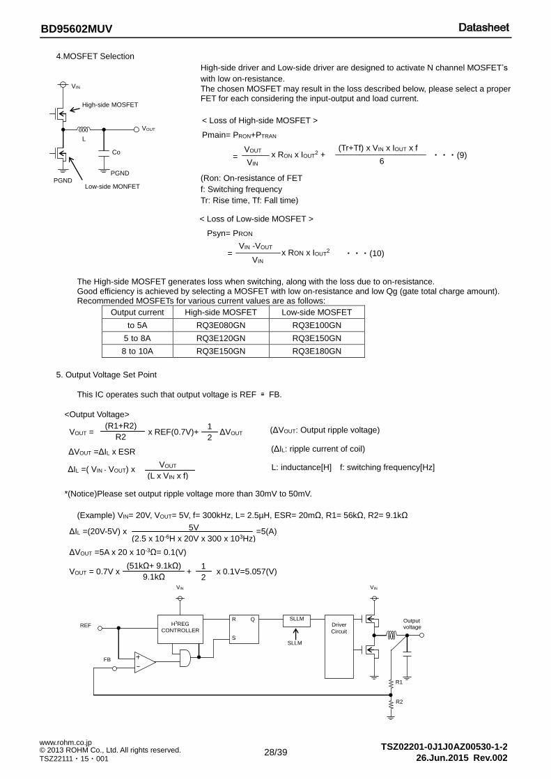
4.MOSFET Selection
The High-side MOSFET generates loss when switching, along with the loss due to on-resistance. Good efficiency is achieved by selecting a MOSFET with low on-resistance and low Qg (gate total charge amount). Recommended MOSFETs for various current values are as follows:
Output current High-side MOSFET Low-side MOSFET
to 5A RQ3E080GN RQ3E100GN
5 to 8A RQ3E120GN RQ3E150GN
8 to 10A RQ3E150GN RQ3E180GN
5. Output Voltage Set Point
This IC operates such that output voltage is REF ≌ FB.
<Output Voltage>
*(Notice)Please set output ripple voltage more than 30mV to 50mV.
(Example) VIN= 20V, VOUT= 5V, f= 300kHz, L= 2.5µH, ESR= 20mΩ, R1= 56kΩ, R2= 9.1kΩ
High-side driver and Low-side driver are designed to activate N channel MOSFET’s
with low on-resistance.
The chosen MOSFET may result in the loss described below, please select a proper FET for each considering the input-output and load current.
(ΔVOUT: Output ripple voltage) (ΔIL: ripple current of coil) L: inductance[H] f: switching frequency[Hz]
ΔVOUT =ΔIL x ESR
ΔIL =( VIN - VOUT) x VOUT
(L x VIN x f)
VOUT = x REF(0.7V)+ ΔVOUT (R1+R2)
R2
1
2
ΔVOUT =5A x 20 x 10-3Ω= 0.1(V)
VOUT = 0.7V x + x 0.1V=5.057(V) 1
2
(51kΩ+ 9.1kΩ)
9.1kΩ
Pmain= PRON+PTRAN
Psyn= PRON
< Loss of High-side MOSFET >
(Ron: On-resistance of FET
f: Switching frequency
Tr: Rise time, Tf: Fall time)
< Loss of Low-side MOSFET >
VOUT
VIN x RON x IOUT
2 + (Tr+Tf) x VIN x IOUT x f
6 = ・・・(9)
VIN -VOUT
VIN x RON x IOUT
2 = ・・・(10)
VIN
L
Co
VOUT
Low-side MONFET
High-side MOSFET
PGND PGND
ΔIL =(20V-5V) x =5(A) 5V
(2.5 x 10-6H x 20V x 300 x 103Hz)
REF
FB
H3REG CONTROLLER
S
R Q SLLM Driver
Circuit
SLLM
VIN
Output voltage
VIN
R1
R2
29/39
TSZ02201-0J1J0AZ00530-1-2
© 2013 ROHM Co., Ltd. All rights reserved. 26.Jun.2015 Rev.002
www.rohm.co.jp
TSZ22111・15・001
BD95602MUV
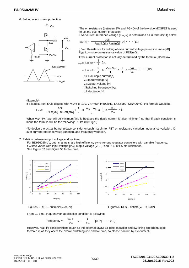
6. Setting over current protection
(Example) If a load current 5A is desired with VIN=6 to 19V, VOUT=5V, f=400kHZ, L=2.5µH, RON=20mΩ, the formula would be:
When VIN= 6V, IOCP will be minimum(this is because the ripple current is also minimum) so that if each condition is input, the formula will be the following: RILIM<109.1[kΩ]. *To design the actual board, please consider enough margin for FET on resistance variation, Inductance variation, IC over current reference value variation, and frequency variation.
7. Relation between output voltage and tON time For BD95602MUV, both channels, are high efficiency synchronous regulator controllers with variable frequency. tON time varies with Input voltage [VIN], output voltage [VOUT], and RFS of FS pin resistance. See Figure 52 and Figure 53 for tON time.
Figure55. RFS – ontime(VOUT= 5V) Figure56. RFS – ontime(VOUT= 3.3V)
From tON time, frequency on application condition is following:
However, real-life considerations (such as the external MOSFET gate capacitor and switching speed) must be factored in as they affect the overall switching rise and fall time, so please confirm by experiment.
The on resistance (between SW and PGND) of the low side MOSFET is used to set the over current protection. Over current reference voltage (ILIM_ref) is determined as in formula(11) below.
(RILIM: Resistance for setting of over current voltage protection value[kΩ] RON: Low-side on resistance value of FET[mΩ])
10k
RILIM[kΩ] x RON[mΩ] ILIM_ref = [A]・・・(11)
Over current protection is actually determined by the formula (12) below.
ΔIL:Coil ripple current[A]
VIN:Input voltage[V]
VO:Output voltage [V]
f:Switching frequency [HZ]
L:Inductance [H]
Coil current
IOCP
ILIM_ref
0
0.5
1
1.5
2
2.5
0 20 40 60 80 100 120
ontim
e[u
s]
RFS[kΩ ]
VIN=7V
VIN=12V
VIN=21V
0
0.5
1
1.5
2
2.5
3
3.5
0 20 40 60 80 100 120
ontim
e[u
s]
RFS[kΩ ]
VIN=7V
VIN=12V
VIN=21V
VOUT
VIN x
1
tON [kHz]・・・(13) Frequency =
ΔIL ILIM_ref + Iocp = 1
2
ILIM_ref + = x 1
2
I
f
VIN - VO
L
x Vo
VIN
x ・・・(12)
VOUT
VIN
L
CO
PGND
SW
RILIM
10k
RILIM[kΩ] ×RON[mΩ] IOCP= + x
1
2
I
f
VIN – VO
L
x VO
VIN
x > 5
30/39
TSZ02201-0J1J0AZ00530-1-2
© 2013 ROHM Co., Ltd. All rights reserved. 26.Jun.2015 Rev.002
www.rohm.co.jp
TSZ22111・15・001
BD95602MUV
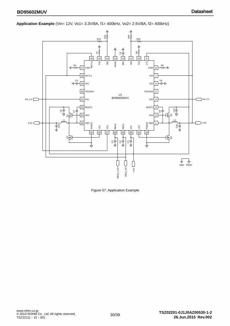
Application Example (Vin= 12V, Vo1= 3.3V/8A, f1= 400kHz, Vo2= 2.5V/8A, f2= 400kHz)
4
5
3
2
1
910
21
20
19
18
17
1112131415
PGOOD1
EN1
BOOT1
HG1
SW1
PGOOD2
EN2
BOOT2
HG2
SW2
RE
G2
RE
G1
VIN
LG
2
PG
ND
2
AG
ND
RE
F
FB
2
FS
2
CT
L
2.5V
EN_3.3BD95602MUV
GND PGND
U1
3.3V
7
8
6
16
24
23
22
31302928272625 32
ILIM2
VO2
SS2
MC
TL2
FS
1
FB
1
ILIM1
MCTL1
SS1
PG
ND
1
LG
1
VO
1
L1
C9
C7
Q1
Q2
C5
R5
C3
C2
C1
C8
L2
C12
Q3
Q4
C6
R6
R7
C4 R8
R16
R26
R15 R25
C19
C29
EN_2.5
RE
G2_3.3
V
RE
G1_5V
+12V
Figure 57. Application Example
U1 BD95602MUV

31/39
TSZ02201-0J1J0AZ00530-1-2
© 2013 ROHM Co., Ltd. All rights reserved. 26.Jun.2015 Rev.002
www.rohm.co.jp
TSZ22111・15・001
BD95602MUV
Without any ripple (about 10mV), there is a possibility that the FB signal is not stable due to the adoption of the comparator control method. Please ensure enough ripple voltage either by (1)reducing the L-value of inductor, or (2)using high ESR output capacitor. Ripple voltage can be generated in FB terminal by adding a capacitor in parallel to resistor (R17, R19) of the FB input, but the circuit will be sensitive to noise from the output (Vo1/Vo2) line and is not recommended. Stability of the circuit is influenced by the layout of the PCB, please pay careful attention to the layout.
Reference Designator
Type Value Description Manufacturer Part Number
Manufacturer Configuration
(mm)
C1, C9, C10, C11, C12
Ceramic Capacitor
10µF 35V, X5R, ±10% GRM32ER6YA106KA12 MURATA 3225
C2, C3, C4 Ceramic
Capacitor 10µF 16V, X5R, ±10% GRM21BR61C106ME15 MURATA 2012
C5, C6 Ceramic
Capacitor 0.1µF 16V, X5R, ±10% GRM155R61C104KA88 MURATA 1005
C7, C8 Ceramic
Capacitor 0.47µF 10V, X5R, ±10% GRM188R61A474KA61 MURATA 1608
C18, C19, C28, C29
POSCAP 330µF 6.3V, ±20%, ESR 18mΩmax
6TPE330MIL SANYO 7343
L1,L2 Inductor 1µH ±20%,10A(L=-30%), DCR=5.8mΩ±10%
GLMC1R003A ALPS 6565
Q1, Q3 MOSFET - N-ch, Vdss 30V, Id 15A, Ron 4.7mΩ
RQ3E150GN ROHM 3333
Q2, Q4 MOSFET - N-ch, Vdss 30V, Id 18A, Ron 3.3mΩ
RQ3E180GN ROHM 3333
R5, R6 Resistor 62kΩ 1/16W, 50V, 5% MCR01MZPJ623 ROHM 1005
R7, R8 Resistor 51kΩ 1/16W, 50V, 5% MCR01MZPJ513 ROHM 1005
R15 Resistor 16kΩ 1/16W, 50V, 0.5% MCR01MZPD1602 ROHM 1005
R16 Resistor 4.3kΩ 1/16W, 50V, 0.5% MCR01MZPD4301 ROHM 1005
R24 Resistor 100Ω 1/16W, 50V, 5% MCR01MZPJ101 ROHM 1005
R25 Resistor 12kΩ 1/16W, 50V, 0.5% MCR01MZPD1202 ROHM 1005
R26 Resistor 4.7kΩ 1/16W, 50V, 0.5% MCR01MZPD4701 ROHM 1005
U1 IC - Buck DC/DC Controller BD95602MUV ROHM VQFN032V5050

32/39
TSZ02201-0J1J0AZ00530-1-2
© 2013 ROHM Co., Ltd. All rights reserved. 26.Jun.2015 Rev.002
www.rohm.co.jp
TSZ22111・15・001
BD95602MUV
Power Dissipation
Ambient Temperature (Ta)
Po
we
r D
issip
atio
n (
Pd)
150 125 100 75 50 25 0
200
400
600
800
1000
[°C]
[mW]
880mW
380mW
θj-a=142. °C /W
85
74.2mm x 74.2mm x 1.6mm Glass-epoxy PCB
IC Only θj-a=328.9°C/W

33/39
TSZ02201-0J1J0AZ00530-1-2
© 2013 ROHM Co., Ltd. All rights reserved. 26.Jun.2015 Rev.002
www.rohm.co.jp
TSZ22111・15・001
BD95602MUV
I/O equivalence circuits
1, 24pin (SW2, SW1) 2, 23pin (HG2, HG1) 3, 22pin (BOOT2, BOOT1)
4, 21pin (EN2, EN1) 5, 20pin (PGOOD2, PGOOD1) 6, 19pin (SS2, SS1)
12pin (REF) 11, 14pin (FB2, FB1) 10, 15pin (FS2, FS1)
16, 18pin (MCTL2, MCTL 1) 9pin (CTL) 26, 31pin (LG1, LG2)
SW
HG
HG BOOT
BOOT BOOT
SW
REG1
50Ω
1MΩ
REG1
REG1
VIN
300kΩ
100kΩ
500kΩ
1MΩ

34/39
TSZ02201-0J1J0AZ00530-1-2
© 2013 ROHM Co., Ltd. All rights reserved. 26.Jun.2015 Rev.002
www.rohm.co.jp
TSZ22111・15・001
BD95602MUV
I/O equivalence circuit(s) - continued
7, 27pin (Vo2, Vo1) 28pin (REG2) 29pin (REG1)
30pin (VIN) 8, 17pin (ILIM2, ILIM1)
50Ω
REG1 VIN VIN

35/39
TSZ02201-0J1J0AZ00530-1-2
© 2013 ROHM Co., Ltd. All rights reserved. 26.Jun.2015 Rev.002
www.rohm.co.jp
TSZ22111・15・001
BD95602MUV
Operational Notes
1. Reverse Connection of Power Supply
Connecting the power supply in reverse polarity can damage the IC. Take precautions against reverse polarity when connecting the power supply, such as mounting an external diode between the power supply and the IC’s power supply pins.
2. Power Supply Lines
Design the PCB layout pattern to provide low impedance supply lines. Separate the ground and supply lines of the digital and analog blocks to prevent noise in the ground and supply lines of the digital block from affecting the analog block. Furthermore, connect a capacitor to ground at all power supply pins. Consider the effect of temperature and aging on the capacitance value when using electrolytic capacitors.
3. Ground Voltage
Ensure that no pins are at a voltage below that of the ground pin at any time, even during transient condition.
4. Ground Wiring Pattern
When using both small-signal and large-current ground traces, the two ground traces should be routed separately but connected to a single ground at the reference point of the application board to avoid fluctuations in the small-signal ground caused by large currents. Also ensure that the ground traces of external components do not cause variations on the ground voltage. The ground lines must be as short and thick as possible to reduce line impedance.
5. Thermal Consideration
Should by any chance the power dissipation rating be exceeded the rise in temperature of the chip may result in
deterioration of the properties of the chip. The absolute maximum rating of the Pd stated in this specification is when
the IC is mounted on a 70mm x 70mm x 1.6mm glass epoxy board. In case of exceeding this absolute maximum
rating, increase the board size and copper area to prevent exceeding the Pd rating.
6. Recommended Operating Conditions
These conditions represent a range within which the expected characteristics of the IC can be approximately obtained. The electrical characteristics are guaranteed under the conditions of each parameter.
7. Inrush Current
When power is first supplied to the IC, it is possible that the internal logic may be unstable and inrush current may flow instantaneously due to the internal powering sequence and delays, especially if the IC has more than one power supply. Therefore, give special consideration to power coupling capacitance, power wiring, width of ground wiring, and routing of connections.
8. Operation Under Strong Electromagnetic Field
Operating the IC in the presence of a strong electromagnetic field may cause the IC to malfunction.
9. Testing on Application Boards
When testing the IC on an application board, connecting a capacitor directly to a low-impedance output pin may subject the IC to stress. Always discharge capacitors completely after each process or step. The IC’s power supply should always be turned off completely before connecting or removing it from the test setup during the inspection process. To prevent damage from static discharge, ground the IC during assembly and use similar precautions during transport and storage.
10. Inter-pin Short and Mounting Errors
Ensure that the direction and position are correct when mounting the IC on the PCB. Incorrect mounting may result in damaging the IC. Avoid nearby pins being shorted to each other especially to ground, power supply and output pin. Inter-pin shorts could be due to many reasons such as metal particles, water droplets (in very humid environment) and unintentional solder bridge deposited in between pins during assembly to name a few.

36/39
TSZ02201-0J1J0AZ00530-1-2
© 2013 ROHM Co., Ltd. All rights reserved. 26.Jun.2015 Rev.002
www.rohm.co.jp
TSZ22111・15・001
BD95602MUV
Operational Notes – continued
11. Unused Input Pins
Input pins of an IC are often connected to the gate of a MOS transistor. The gate has extremely high impedance and extremely low capacitance. If left unconnected, the electric field from the outside can easily charge it. The small charge acquired in this way is enough to produce a significant effect on the conduction through the transistor and cause unexpected operation of the IC. So unless otherwise specified, unused input pins should be connected to the power supply or ground line.
12. Regarding the Input Pin of the IC
This monolithic IC contains P+ isolation and P substrate layers between adjacent elements in order to keep them isolated. P-N junctions are formed at the intersection of the P layers with the N layers of other elements, creating a parasitic diode or transistor. For example (refer to figure below):
When GND > Pin A and GND > Pin B, the P-N junction operates as a parasitic diode. When GND > Pin B, the P-N junction operates as a parasitic transistor.
Parasitic diodes inevitably occur in the structure of the IC. The operation of parasitic diodes can result in mutual interference among circuits, operational faults, or physical damage. Therefore, conditions that cause these diodes to operate, such as applying a voltage lower than the GND voltage to an input pin (and thus to the P substrate) should be avoided.
Figure 58. Example of monolithic IC structure
13. Ceramic Capacitor
When using a ceramic capacitor, determine the dielectric constant considering the change of capacitance with temperature and the decrease in nominal capacitance due to DC bias and others.
14. Area of Safe Operation (ASO)
Operate the IC such that the output voltage, output current, and power dissipation are all within the Area of Safe Operation (ASO).
15. Thermal Shutdown Circuit(TSD)
This IC has a built-in thermal shutdown circuit that prevents heat damage to the IC. Normal operation should always be within the IC’s power dissipation rating. If however the rating is exceeded for a continued period, the junction temperature (Tj) will rise which will activate the TSD circuit that will turn OFF all output pins. When the Tj falls below the TSD threshold, the circuits are automatically restored to normal operation. Note that the TSD circuit operates in a situation that exceeds the absolute maximum ratings and therefore, under no circumstances, should the TSD circuit be used in a set design or for any purpose other than protecting the IC from heat damage.
16. Over Current Protection Circuit (OCP)
This IC incorporates an integrated overcurrent protection circuit that is activated when the load is shorted. This protection circuit is effective in preventing damage due to sudden and unexpected incidents. However, the IC should not be used in applications characterized by continuous operation or transitioning of the protection circuit.
N NP
+ P
N NP
+
P Substrate
GND
NP
+
N NP
+N P
P Substrate
GND GND
Parasitic
Elements
Pin A
Pin A
Pin B Pin B
B C
E
Parasitic
Elements
GNDParasitic
Elements
CB
E
Transistor (NPN)Resistor
N Region
close-by
Parasitic
Elements
37/39
TSZ02201-0J1J0AZ00530-1-2
© 2013 ROHM Co., Ltd. All rights reserved. 26.Jun.2015 Rev.002
www.rohm.co.jp
TSZ22111・15・001
BD95602MUV
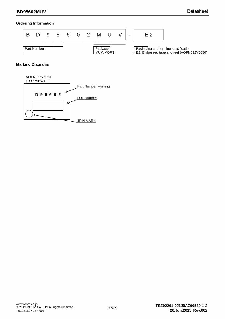
Ordering Information
B D 9 5 6 0 2 M U V - E 2
Part Number
Package MUV: VQFN
Packaging and forming specification E2: Embossed tape and reel (VQFN032V5050)
Marking Diagrams
VQFN032V5050 (TOP VIEW)
D 9 5 6 0 2
Part Number Marking
LOT Number
1PIN MARK

38/39
TSZ02201-0J1J0AZ00530-1-2
© 2013 ROHM Co., Ltd. All rights reserved. 26.Jun.2015 Rev.002
www.rohm.co.jp
TSZ22111・15・001
BD95602MUV
Physical Dimension, Tape and Reel Information
Package Name VQFN032V5050
39/39
TSZ02201-0J1J0AZ00530-1-2
© 2013 ROHM Co., Ltd. All rights reserved. 26.Jun.2015 Rev.002
www.rohm.co.jp
TSZ22111・15・001
BD95602MUV
Revision History
Date Revision Changes
6.Sep.2013 001 New Release
26.Jun.2015 002 P.31 Change ‘’the description’’ of L1,L2

DatasheetDatasheet
Notice-PGA-E Rev.001© 2015 ROHM Co., Ltd. All rights reserved.
Notice Precaution on using ROHM Products
1. Our Products are designed and manufactured for application in ordinary electronic equipments (such as AV equipment, OA equipment, telecommunication equipment, home electronic appliances, amusement equipment, etc.). If you intend to use our Products in devices requiring extremely high reliability (such as medical equipment (Note 1), transport equipment, traffic equipment, aircraft/spacecraft, nuclear power controllers, fuel controllers, car equipment including car accessories, safety devices, etc.) and whose malfunction or failure may cause loss of human life, bodily injury or serious damage to property (“Specific Applications”), please consult with the ROHM sales representative in advance. Unless otherwise agreed in writing by ROHM in advance, ROHM shall not be in any way responsible or liable for any damages, expenses or losses incurred by you or third parties arising from the use of any ROHM’s Products for Specific Applications.
(Note1) Medical Equipment Classification of the Specific Applications JAPAN USA EU CHINA
CLASSⅢ CLASSⅢ
CLASSⅡb CLASSⅢ
CLASSⅣ CLASSⅢ
2. ROHM designs and manufactures its Products subject to strict quality control system. However, semiconductor
products can fail or malfunction at a certain rate. Please be sure to implement, at your own responsibilities, adequate safety measures including but not limited to fail-safe design against the physical injury, damage to any property, which a failure or malfunction of our Products may cause. The following are examples of safety measures:
[a] Installation of protection circuits or other protective devices to improve system safety [b] Installation of redundant circuits to reduce the impact of single or multiple circuit failure
3. Our Products are designed and manufactured for use under standard conditions and not under any special or extraordinary environments or conditions, as exemplified below. Accordingly, ROHM shall not be in any way responsible or liable for any damages, expenses or losses arising from the use of any ROHM’s Products under any special or extraordinary environments or conditions. If you intend to use our Products under any special or extraordinary environments or conditions (as exemplified below), your independent verification and confirmation of product performance, reliability, etc, prior to use, must be necessary:
[a] Use of our Products in any types of liquid, including water, oils, chemicals, and organic solvents [b] Use of our Products outdoors or in places where the Products are exposed to direct sunlight or dust [c] Use of our Products in places where the Products are exposed to sea wind or corrosive gases, including Cl2,
H2S, NH3, SO2, and NO2
[d] Use of our Products in places where the Products are exposed to static electricity or electromagnetic waves [e] Use of our Products in proximity to heat-producing components, plastic cords, or other flammable items [f] Sealing or coating our Products with resin or other coating materials [g] Use of our Products without cleaning residue of flux (even if you use no-clean type fluxes, cleaning residue of
flux is recommended); or Washing our Products by using water or water-soluble cleaning agents for cleaning residue after soldering
[h] Use of the Products in places subject to dew condensation
4. The Products are not subject to radiation-proof design. 5. Please verify and confirm characteristics of the final or mounted products in using the Products. 6. In particular, if a transient load (a large amount of load applied in a short period of time, such as pulse. is applied,
confirmation of performance characteristics after on-board mounting is strongly recommended. Avoid applying power exceeding normal rated power; exceeding the power rating under steady-state loading condition may negatively affect product performance and reliability.
7. De-rate Power Dissipation (Pd) depending on Ambient temperature (Ta). When used in sealed area, confirm the actual
ambient temperature. 8. Confirm that operation temperature is within the specified range described in the product specification. 9. ROHM shall not be in any way responsible or liable for failure induced under deviant condition from what is defined in
this document.
Precaution for Mounting / Circuit board design 1. When a highly active halogenous (chlorine, bromine, etc.) flux is used, the residue of flux may negatively affect product
performance and reliability.
2. In principle, the reflow soldering method must be used on a surface-mount products, the flow soldering method must be used on a through hole mount products. If the flow soldering method is preferred on a surface-mount products, please consult with the ROHM representative in advance.
For details, please refer to ROHM Mounting specification

DatasheetDatasheet
Notice-PGA-E Rev.001© 2015 ROHM Co., Ltd. All rights reserved.
Precautions Regarding Application Examples and External Circuits 1. If change is made to the constant of an external circuit, please allow a sufficient margin considering variations of the
characteristics of the Products and external components, including transient characteristics, as well as static characteristics.
2. You agree that application notes, reference designs, and associated data and information contained in this document
are presented only as guidance for Products use. Therefore, in case you use such information, you are solely responsible for it and you must exercise your own independent verification and judgment in the use of such information contained in this document. ROHM shall not be in any way responsible or liable for any damages, expenses or losses incurred by you or third parties arising from the use of such information.
Precaution for Electrostatic
This Product is electrostatic sensitive product, which may be damaged due to electrostatic discharge. Please take proper caution in your manufacturing process and storage so that voltage exceeding the Products maximum rating will not be applied to Products. Please take special care under dry condition (e.g. Grounding of human body / equipment / solder iron, isolation from charged objects, setting of Ionizer, friction prevention and temperature / humidity control).
Precaution for Storage / Transportation 1. Product performance and soldered connections may deteriorate if the Products are stored in the places where:
[a] the Products are exposed to sea winds or corrosive gases, including Cl2, H2S, NH3, SO2, and NO2 [b] the temperature or humidity exceeds those recommended by ROHM [c] the Products are exposed to direct sunshine or condensation [d] the Products are exposed to high Electrostatic
2. Even under ROHM recommended storage condition, solderability of products out of recommended storage time period may be degraded. It is strongly recommended to confirm solderability before using Products of which storage time is exceeding the recommended storage time period.
3. Store / transport cartons in the correct direction, which is indicated on a carton with a symbol. Otherwise bent leads
may occur due to excessive stress applied when dropping of a carton. 4. Use Products within the specified time after opening a humidity barrier bag. Baking is required before using Products of
which storage time is exceeding the recommended storage time period.
Precaution for Product Label QR code printed on ROHM Products label is for ROHM’s internal use only.
Precaution for Disposition When disposing Products please dispose them properly using an authorized industry waste company.
Precaution for Foreign Exchange and Foreign Trade act Since concerned goods might be fallen under listed items of export control prescribed by Foreign exchange and Foreign trade act, please consult with ROHM in case of export.
Precaution Regarding Intellectual Property Rights 1. All information and data including but not limited to application example contained in this document is for reference
only. ROHM does not warrant that foregoing information or data will not infringe any intellectual property rights or any other rights of any third party regarding such information or data.
2. ROHM shall not have any obligations where the claims, actions or demands arising from the combination of the Products with other articles such as components, circuits, systems or external equipment (including software).
3. No license, expressly or implied, is granted hereby under any intellectual property rights or other rights of ROHM or any third parties with respect to the Products or the information contained in this document. Provided, however, that ROHM will not assert its intellectual property rights or other rights against you or your customers to the extent necessary to manufacture or sell products containing the Products, subject to the terms and conditions herein.
Other Precaution 1. This document may not be reprinted or reproduced, in whole or in part, without prior written consent of ROHM.
2. The Products may not be disassembled, converted, modified, reproduced or otherwise changed without prior written consent of ROHM.
3. In no event shall you use in any way whatsoever the Products and the related technical information contained in the Products or this document for any military purposes, including but not limited to, the development of mass-destruction weapons.
4. The proper names of companies or products described in this document are trademarks or registered trademarks of ROHM, its affiliated companies or third parties.

DatasheetDatasheet
Notice – WE Rev.001© 2015 ROHM Co., Ltd. All rights reserved.
General Precaution 1. Before you use our Pro ducts, you are requested to care fully read this document and fully understand its contents.
ROHM shall n ot be in an y way responsible or liabl e for fa ilure, malfunction or acci dent arising from the use of a ny ROHM’s Products against warning, caution or note contained in this document.
2. All information contained in this docume nt is current as of the issuing date and subj ect to change without any prior
notice. Before purchasing or using ROHM’s Products, please confirm the la test information with a ROHM sale s representative.
3. The information contained in this doc ument is provi ded on an “as is” basis and ROHM does not warrant that all
information contained in this document is accurate an d/or error-free. ROHM shall not be in an y way responsible or liable for any damages, expenses or losses incurred by you or third parties resulting from inaccuracy or errors of or concerning such information.