Embed Size (px)
Citation preview

5.5 V Input, 300 mA, Low Quiescent Current, CMOS Linear Regulator
Data Sheet ADP122/ADP123
Rev. E Information furnished by Analog Devices is believed to be accurate and reliable. However, no responsibility is assumed by Analog Devices for its use, nor for any infringements of patents or other rights of third parties that may result from its use. Specifications subject to change without notice. No license is granted by implication or otherwise under any patent or patent rights of Analog Devices. Trademarks and registered trademarks are the property of their respective owners.
One Technology Way, P.O. Box 9106, Norwood, MA 02062-9106, U.S.A. Tel: 781.329.4700 www.analog.com Fax: 781.461.3113 ©2009–2012 Analog Devices, Inc. All rights reserved.
FEATURES Input voltage supply range: 2.3 V to 5.5 V 300 mA maximum output current Fixed and adjustable output voltage versions Very low dropout voltage: 85 mV at 300 mA load Low quiescent current: 45 µA at no load Low shutdown current: <1 µA Initial accuracy: ±1% accuracy Up to 31 fixed-output voltage options available from
1.75 V to 3.3 V Adjustable-output voltage range
0.8 V to 5.0 V (ADP123) Excellent PSRR performance: 60 dB at 100 kHz Excellent load/line transient response Optimized for small 1.0 μF ceramic capacitors Current limit and thermal overload protection Logic controlled enable Compact packages: 5-lead TSOT and 6-lead 2 mm × 2 mm LFCSP
APPLICATIONS Digital camera and audio devices Portable and battery-powered equipment Automatic meter reading (AMR) meters GPS and location management units Medical instrumentation Point-of-sale equipment
GENERAL DESCRIPTION The ADP122/ADP123 are low quiescent current, low dropout linear regulators. They are designed to operate from an input voltage between 2.3 V and 5.5 V and to provide up to 300 mA of output current. The low 85 mV dropout voltage at a 300 mA load improves efficiency and allows operation over a wide input voltage range.
The low 170 μA of quiescent current at full load makes the ADP122 ideal for battery-operated portable equipment.
The ADP122 is capable of 31 fixed output voltages from 1.75 V to 3.3 V. The ADP123 is the adjustable version of the device and allows the output voltage to be set between 0.8 V and 5.0 V by an external voltage divider.
The ADP122/ADP123 are specifically designed for stable operation with tiny 1 µF ceramic input and output capacitors to meet the requirements of high performance, space constrained applications.
TYPICAL APPLICATION CIRCUITS
2
3
1
4
5VIN = 2.3V TO 5.5V VOUT = 1.8V
VIN
GND
EN
VOUT
NC
CIN1µF
COUT1µFADP122
0839
9-00
1
OFF
ON
Figure 1. ADP122 with Fixed Output Voltage (TSOT Version)
VIN = 2.3V TO 5.5V VOUT = 0.5V(1 + R1/R2)
R1
R2
CIN1µF
COUT1µF
0839
9-00
2
2
3
1
4
5VIN
GND
EN
VOUT
ADJ
ADP123
OFF
ON
Figure 2. ADP123 with Adjustable Output Voltage (TSOT Version)
0839
9-13
5
NC = NOT CONNECT. THIS PIN CAN BE LEFT FLOATINGOR CONNECTED TO GROUND.
TOP VIEW(Not to Scale)
ADP122
3GND
1VOUT
2 NC
4EN
6 VIN = 2.3V TO 5.5VVOUT = 1.8V
C11µFGND
ONOFF
VIN
5NC
C21µFGND
GND
Figure 3. ADP122 with Fixed Output Voltage (LFCSP Version)
0839
9-13
6
NC = NOT CONNECT. THIS PIN CAN BE LEFT FLOATINGOR CONNECTED TO GROUND.
TOP VIEW(Not to Scale)
ADP123
3GND
1VOUT
2ADJ
4EN
6 VIN = 2.3V TO 5.5VVOUT = 0.5V (1 + R1/R2)
C11µFGND
ONOFF
VIN
5NC
C21µF R1
R2GND
GND
GND
Figure 4. ADP123 with Adjustable Output Voltage (LFCSP Version)
The ADP122/ADP123 have an internal soft start that gives a constant start-up time of 350 µs. Short-circuit protection and thermal overload protection circuits prevent damage in adverse conditions. The ADP122/ADP123 are available in a tiny, 5-lead TSOT package and 6-lead LFCSP package for the smallest footprint solution to meet a variety of portable applications.
ADP122/ADP123 Data Sheet
Rev. E | Page 2 of 24
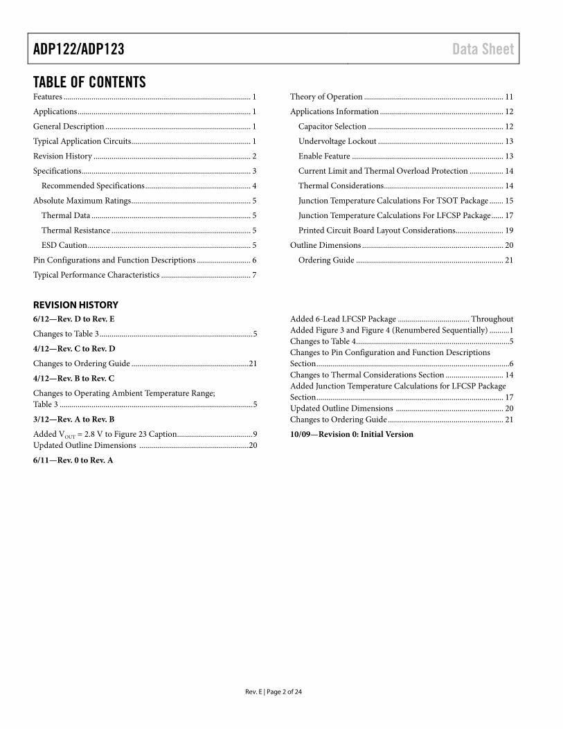
TABLE OF CONTENTS Features .............................................................................................. 1 Applications ....................................................................................... 1 General Description ......................................................................... 1 Typical Application Circuits ............................................................ 1 Revision History ............................................................................... 2 Specifications ..................................................................................... 3
Recommended Specifications ..................................................... 4 Absolute Maximum Ratings ............................................................ 5
Thermal Data ................................................................................ 5 Thermal Resistance ...................................................................... 5 ESD Caution .................................................................................. 5
Pin Configurations and Function Descriptions ........................... 6 Typical Performance Characteristics ............................................. 7
Theory of Operation ...................................................................... 11 Applications Information .............................................................. 12
Capacitor Selection .................................................................... 12 Undervoltage Lockout ............................................................... 13 Enable Feature ............................................................................ 13 Current Limit and Thermal Overload Protection ................. 14 Thermal Considerations ............................................................ 14 Junction Temperature Calculations For TSOT Package ....... 15 Junction Temperature Calculations For LFCSP Package ...... 17 Printed Circuit Board Layout Considerations........................ 19
Outline Dimensions ....................................................................... 20 Ordering Guide .......................................................................... 21
REVISION HISTORY 6/12—Rev. D to Rev. E
Changes to Table 3 ............................................................................. 5
4/12—Rev. C to Rev. D
Changes to Ordering Guide ........................................................... 21
4/12—Rev. B to Rev. C
Changes to Operating Ambient Temperature Range; Table 3 ................................................................................................. 5
3/12—Rev. A to Rev. B
Added VOUT = 2.8 V to Figure 23 Caption...................................... 9 Updated Outline Dimensions ....................................................... 20
6/11—Rev. 0 to Rev. A
Added 6-Lead LFCSP Package .................................... Throughout Added Figure 3 and Figure 4 (Renumbered Sequentially) .......... 1 Changes to Table 4 ............................................................................. 5 Changes to Pin Configuration and Function Descriptions Section ................................................................................................. 6 Changes to Thermal Considerations Section ............................. 14 Added Junction Temperature Calculations for LFCSP Package Section .............................................................................................. 17 Updated Outline Dimensions ...................................................... 20 Changes to Ordering Guide .......................................................... 21
10/09—Revision 0: Initial Version

Data Sheet ADP122/ADP123
Rev. E | Page 3 of 24
SPECIFICATIONS Unless otherwise noted, VIN = (VOUT + 0.3 V) or 2.3 V, whichever is greater; ADJ connected to VOUT; IOUT = 10 mA; CIN = 1.0 µF; COUT = 1.0 µF; TA = 25°C.
Table 1. Parameter Symbol Test Conditions Min Typ Max Unit INPUT VOLTAGE RANGE VIN 2.3 5.5 V OPERATING SUPPLY CURRENT1 IGND IOUT = 0 µA 45 µA
IOUT = 0 µA, TJ = −40°C to +125°C 105 µA IOUT = 1 mA 60 µA IOUT = 1 mA, TJ = −40°C to +125°C 120 µA IOUT = 150 mA 130 µA IOUT = 150 mA, TJ = −40°C to +125°C 190 µA IOUT = 300 mA 170 µA IOUT = 300 mA, TJ = −40°C to +125°C 240 µA
SHUTDOWN CURRENT ISD EN = GND 0.1 µA EN = GND, TJ = −40°C to +125°C 1 µA
OUTPUT VOLTAGE ACCURACY2 VOUT Fixed Output IOUT = 10 mA −1 +1 % 100 µA < IOUT < 300 mA, VIN = (VOUT + 0.5 V) to 5.5 V,
TJ = −40°C to +125°C −2 +1.5 %
Adjustable Output IOUT = 10 mA 0.495 0.500 0.505 V 100 µA < IOUT < 300 mA, VIN = 2.3 V to 5.5 V,
TJ = −40°C to +125°C 0.490 0.500 0.5075 V
LINE REGULATION ∆VOUT/∆VIN VIN = VIN = 2.3 V to 5.5 V, TJ = −40°C to +125°C −0.05 +0.05 %/V LOAD REGULATION3 ∆VOUT/∆IOUT IOUT = 1 mA to 300 mA 0.0005 %/mA
IOUT = 1 mA to 300 mA , TJ = −40°C to +125°C 0.001 %/mA ADJ INPUT BIAS CURRENT ADJI-BIAS 2.3 V ≤ VIN ≤ 5.5 V, ADJ connected to VOUT 15 nA DROPOUT VOLTAGE4 VDROPOUT
IOUT = 10 mA, VOUT > 2.3 V 3 mV IOUT = 10 mA, TJ = −40°C to +125°C 5 mV IOUT = 150 mA, VOUT > 2.3 V 45 mV IOUT = 150 mA, TJ = −40°C to +125°C 75 mV IOUT = 300 mA, VOUT > 2.3V 85 mV IOUT = 300 mA, TJ = −40°C to +125°C 150 mV
START-UP TIME5 tSTART-UP VOUT = 3.0 V 350 µs CURRENT LIMIT THRESHOLD6 ILIMIT 350 500 650 mA THERMAL SHUTDOWN
Thermal Shutdown Threshold TSSD TJ rising 150 °C Thermal Shutdown Hysteresis TSSD-HYS 15 °C
EN INPUT EN Input Logic High VIH 2.3 V ≤ VIN ≤ 5.5 V 1.2 V EN Input Logic Low VIL 2.3 V ≤ VIN ≤ 5.5 V 0.4 V EN Input Leakage Current VI-LEAKAGE EN = VIN or GND 0.1 µA EN = VIN or GND, TJ = −40°C to +125°C 1 µA
UNDERVOLTAGE LOCKOUT UVLO Input Voltage Rising UVLORISE TJ = −40°C to +125°C 2.1 V Input Voltage Falling UVLOFALL TJ = −40°C to +125°C 1.5 V Hysteresis UVLOHYS TA = 25°C 125 mV

ADP122/ADP123 Data Sheet
Rev. E | Page 4 of 24
Parameter Symbol Test Conditions Min Typ Max Unit OUTPUT NOISE OUTNOISE 10 Hz to 100 kHz, VIN = 5.5 V, VOUT = 1.2 V 25 µV rms 10 Hz to 100 kHz, VIN = 5.5 V, VOUT = 1.8 V 35 µV rms
10 Hz to 100 kHz, VIN = 5.5 V, VOUT = 2.5 V 45 µV rms 10 Hz to 100 kHz, VIN = 5.5 V, VOUT = 3.3 V 55 µV rms 10 Hz to 100 kHz, VIN = 5.5 V, VOUT = 4.2 V 65 µV rms
POWER SUPPLY REJECTION RATIO PSRR 10 kHz, VOUT = 3.3 V 60 dB (VIN = VOUT + 0.5 V) 10 kHz, VOUT = 2.5 V 60 dB 10 kHz, VOUT = 1.8 V 60 dB 100 kHz, VOUT = 3.3 V 60 dB 100 kHz, VOUT = 2.5 V 60 dB 100 kHz, VOUT = 1.8 V 60 dB
1 The current from the external resistor divider network in the case of adjustable voltage output (as with the ADP123) should be subtracted from the ground current measured. 2 Accuracy when VOUT is connected directly to ADJ. When VOUT voltage is set by external feedback resistors, absolute accuracy in adjust mode depends on the tolerances of
the resistors used. 3 Based on an endpoint calculation using 1 mA and 300 mA loads. 4 Dropout voltage is defined as the input-to-output voltage differential when the input voltage is set to the nominal output voltage. This applies only for output voltages
greater than 2.3 V. 5 Start-up time is defined as the time between the rising edge of EN to VOUT being at 90% of its nominal value. 6 Current limit threshold is defined as the current at which the output voltage drops to 90% of the specified typical value. For example, the current limit for a 3.3 V
output voltage is defined as the current that causes the output voltage to drop to 90% of 3.3V, or 2.97 V.
RECOMMENDED SPECIFICATIONS
Table 2. Parameter Symbol Test Conditions Min Typ Max Unit Minimum Input and Output
Capacitance1 CAPMIN TA = −40°C to +125°C 0.70 µF
Capacitor ESR RESR TA = −40°C to +125°C 0.001 1 Ω 1 The minimum input and output capacitance should be greater than 0.70 µF over the full range of operating conditions. The full range of operating conditions in the
application must be considered during device selection to ensure that the minimum capacitance specification is met. X7R and X5R type capacitors are recommended; Y5V and Z5U capacitors are not recommended for use with any LDO.
Data Sheet ADP122/ADP123
Rev. E | Page 5 of 24
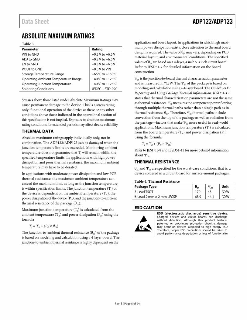
ABSOLUTE MAXIMUM RATINGS Table 3. Parameter Rating VIN to GND −0.3 V to +6.5 V ADJ to GND −0.3 V to +6.5 V EN to GND −0.3 V to +6.5 V VOUT to GND −0.3 V to VIN Storage Temperature Range −65°C to +150°C Operating Ambient Temperature Range −40°C to +125°C Operating Junction Temperature −40°C to +125°C Soldering Conditions JEDEC J-STD-020
Stresses above those listed under Absolute Maximum Ratings may cause permanent damage to the device. This is a stress rating only; functional operation of the device at these or any other conditions above those indicated in the operational section of this specification is not implied. Exposure to absolute maximum rating conditions for extended periods may affect device reliability.
THERMAL DATA Absolute maximum ratings apply individually only, not in combination. The ADP122/ADP123 can be damaged when the junction temperature limits are exceeded. Monitoring ambient temperature does not guarantee that TJ will remain within the specified temperature limits. In applications with high power dissipation and poor thermal resistance, the maximum ambient temperature may have to be derated.
In applications with moderate power dissipation and low PCB thermal resistance, the maximum ambient temperature can exceed the maximum limit as long as the junction temperature is within specification limits. The junction temperature (TJ) of the device is dependent on the ambient temperature (TA), the power dissipation of the device (PD), and the junction-to-ambient thermal resistance of the package (θJA).
Maximum junction temperature (TJ) is calculated from the ambient temperature (TA) and power dissipation (PD) using the formula
TJ = TA + (PD × θJA)
The junction-to-ambient thermal resistance (θJA) of the package is based on modeling and calculation using a 4-layer board. The junction-to-ambient thermal resistance is highly dependent on the
application and board layout. In applications in which high maxi-mum power dissipation exists, close attention to thermal board design is required. The value of θJA may vary, depending on PCB material, layout, and environmental conditions. The specified values of θJA are based on a 4-layer, 4 inch × 3 inch circuit board. Refer to JESD51-7 for detailed information on the board construction
ΨJB is the junction-to-board thermal characterization parameter and is measured in °C/W. The ΨJB of the package is based on modeling and calculation using a 4-layer board. The Guidelines for Reporting and Using Package Thermal Information: JESD51-12 states that thermal characterization parameters are not the same as thermal resistances. ΨJB measures the component power flowing through multiple thermal paths rather than a single path as in thermal resistance, θJB. Therefore, ΨJB thermal paths include convection from the top of the package as well as radiation from the package—factors that make ΨJB more useful in real-world applications. Maximum junction temperature (TJ) is calculated from the board temperature (TB) and power dissipation (PD) using the formula
TJ = TB + (PD × ΨJB)
Refer to JESD51-8 and JESD51-12 for more detailed information about ΨJB.
THERMAL RESISTANCE θJA and ΨJB are specified for the worst-case conditions, that is, a device soldered in a circuit board for surface-mount packages.
Table 4. Thermal Resistance Package Type θJA ΨJB Unit 5-Lead TSOT 170 43 °C/W 6-Lead 2 mm × 2 mm LFCSP 68.9 44.1 °C/W
ESD CAUTION
ADP122/ADP123 Data Sheet
Rev. E | Page 6 of 24
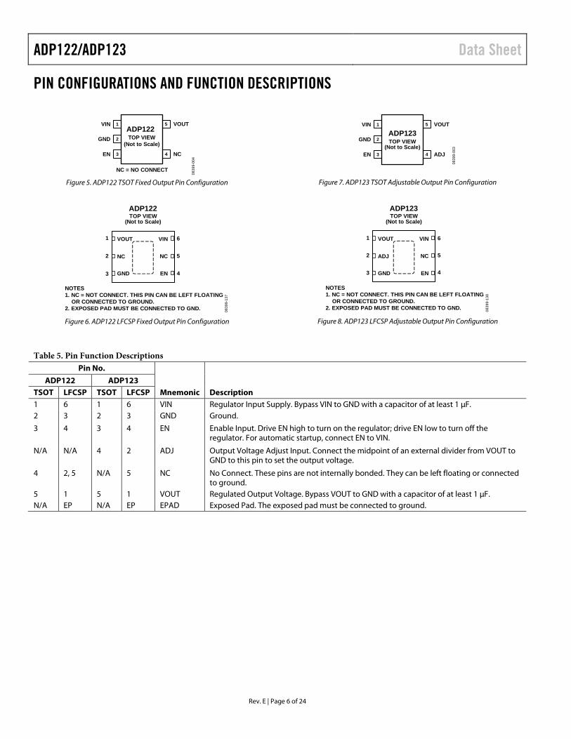
PIN CONFIGURATIONS AND FUNCTION DESCRIPTIONS
ADP122TOP VIEW
(Not to Scale)
1VIN
2GND
3EN
5 VOUT
4 NC
NC = NO CONNECT
0839
9-00
4
Figure 5. ADP122 TSOT Fixed Output Pin Configuration
0839
9-13
7
TOP VIEW(Not to Scale)
ADP122
3 GND
1 VOUT
2 NC
4EN
6VIN
5NC
NOTES1. NC = NOT CONNECT. THIS PIN CAN BE LEFT FLOATING OR CONNECTED TO GROUND.2. EXPOSED PAD MUST BE CONNECTED TO GND.
Figure 6. ADP122 LFCSP Fixed Output Pin Configuration
ADP123TOP VIEW
(Not to Scale)
1VIN
2GND
3EN
5 VOUT
4 ADJ
0839
9-00
3
Figure 7. ADP123 TSOT Adjustable Output Pin Configuration
0839
9-13
8
TOP VIEW(Not to Scale)
ADP123
3 GND
1 VOUT
2 ADJ
4EN
6
NOTES1. NC = NOT CONNECT. THIS PIN CAN BE LEFT FLOATING OR CONNECTED TO GROUND.2. EXPOSED PAD MUST BE CONNECTED TO GND.
VIN
5NC
Figure 8. ADP123 LFCSP Adjustable Output Pin Configuration
Table 5. Pin Function Descriptions Pin No.
Mnemonic Description ADP122 ADP123
TSOT LFCSP TSOT LFCSP 1 6 1 6 VIN Regulator Input Supply. Bypass VIN to GND with a capacitor of at least 1 µF. 2 3 2 3 GND Ground.
3 4 3 4 EN Enable Input. Drive EN high to turn on the regulator; drive EN low to turn off the regulator. For automatic startup, connect EN to VIN.
N/A N/A 4 2 ADJ Output Voltage Adjust Input. Connect the midpoint of an external divider from VOUT to GND to this pin to set the output voltage.
4 2, 5 N/A 5 NC No Connect. These pins are not internally bonded. They can be left floating or connected to ground.
5 1 5 1 VOUT Regulated Output Voltage. Bypass VOUT to GND with a capacitor of at least 1 µF. N/A EP N/A EP EPAD Exposed Pad. The exposed pad must be connected to ground.

Data Sheet ADP122/ADP123
Rev. E | Page 7 of 24
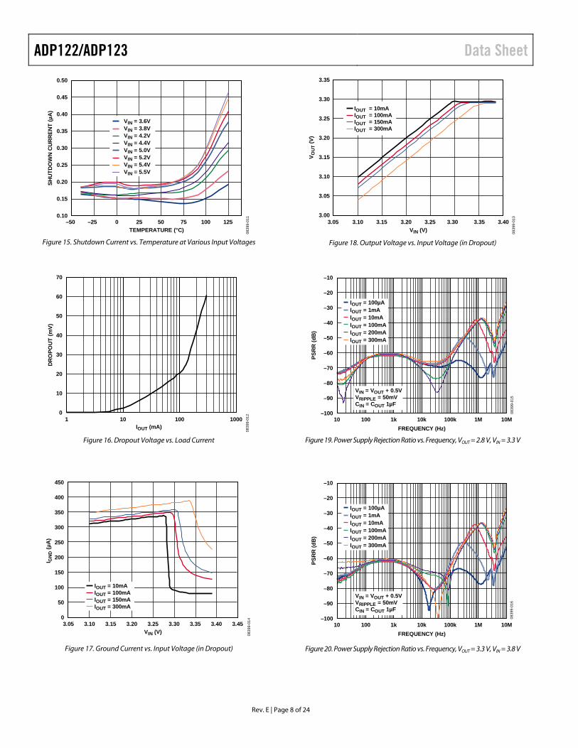
TYPICAL PERFORMANCE CHARACTERISTICS VIN = 3.6 V, VOUT = 3.3 V, IOUT = 10 mA, CIN = 1.0 µF, COUT = 1.0 µF, TA = 25°C, unless otherwise noted.
3.260
3.265
3.270
3.275
3.280
3.285
3.290
3.295
3.300
–40 –5 25 85 125JUNCTION TEMPERATURE (°C)
V OU
T (V
)
IOUT = 100µAIOUT = 1mAIOUT = 10mAIOUT = 100mAIOUT = 200mAIOUT = 300mA
0839
9-00
5
Figure 9. Output Voltage vs. Junction Temperature
3.2895
3.2900
3.2905
3.2910
3.2915
3.2920
3.2925
3.2930
3.2935
3.2940
3.2945
0.1 1 10 100 1000IOUT (mA)
V OU
T(V
)
0839
9-00
6
Figure 10. Output Voltage vs. Load Current
3.284
3.286
3.288
3.290
3.292
3.294
3.296
VIN (V)
V OU
T (V
)
0839
9-00
7
3.6 3.8 4.0 4.2 4.4 4.6 4.8 5.0 5.2 5.4
IOUT = 100µAIOUT = 1mAIOUT = 10mAIOUT = 100mAIOUT = 200mAIOUT = 300mA
Figure 11. Output Voltage vs. Input Voltage
0
50
100
150
200
250
GR
OU
ND
CU
RR
ENT
(µA
)
–40 –5 25 85 125JUNCTION TEMPERATURE (°C)
IOUT = 100µA
IOUT = 10mA
IOUT = 100mA
IOUT = 200mA
IOUT = 300mA
IOUT = 1mA
0839
9-00
8
Figure 12. Ground Current vs. Junction Temperature
0
20
40
60
80
100
120
140
160
180
200
0.1 1 10 100 1000IOUT (mA)
GR
OU
ND
CU
RR
ENT
(µA
)
0839
9-00
9
Figure 13. Ground Current vs. Load Current
0
20
40
60
80
100
120
140
160
180
200
3.6 3.8 4.0 4.2 4.4 4.6 4.8 5.0 5.2 5.4VIN (V)
GR
OU
ND
CU
RR
ENT
(µA
)
IOUT = 100µA
IOUT = 1mA
IOUT = 10mA
IOUT = 100mA
IOUT = 200mA
IOUT = 300mA08
399-
010
Figure 14. Ground Current vs. Input Voltage
ADP122/ADP123 Data Sheet
Rev. E | Page 8 of 24
0.10
0.15
0.20
0.25
0.30
0.35
0.40
0.45
0.50
–50 –25 0 25 50 75 100 125TEMPERATURE (°C)
SHU
TDO
WN
CU
RR
ENT
(µA
)
VIN = 3.6VVIN = 3.8VVIN = 4.2VVIN = 4.4VVIN = 5.0VVIN = 5.2VVIN = 5.4VVIN = 5.5V
0839
9-01
1
Figure 15. Shutdown Current vs. Temperature at Various Input Voltages
0
10
20
30
40
50
60
70
1 10 100 1000IOUT (mA)
DR
OPO
UT
(mV)
0839
9-01
2
Figure 16. Dropout Voltage vs. Load Current
0
50
100
150
200
250
300
350
400
450
3.05 3.10 3.15 3.20 3.25 3.30 3.35 3.40 3.45VIN (V)
I GN
D (µ
A)
IOUT = 10mAIOUT = 100mAIOUT = 150mAIOUT = 300mA
0839
9-01
4
Figure 17. Ground Current vs. Input Voltage (in Dropout)
3.00
3.05
3.10
3.15
3.20
3.25
3.30
3.35
3.05 3.10 3.15 3.20 3.25 3.30 3.35 3.40VIN (V)
V OU
T (V
)
IOUT = 10mAIOUT = 100mAIOUT = 150mAIOUT = 300mA
0839
9-01
3
Figure 18. Output Voltage vs. Input Voltage (in Dropout)
–100
–90
–80
–70
–60
–50
–40
–30
–20
–10
10 100 1k 10k 100k 1M 10MFREQUENCY (Hz)
PSR
R (d
B)
IOUT = 100µA
VIN = VOUT + 0.5VVRIPPLE = 50mVCIN = COUT 1µF
IOUT = 1mAIOUT = 10mAIOUT = 100mAIOUT = 200mAIOUT = 300mA
0839
9-01
5
Figure 19. Power Supply Rejection Ratio vs. Frequency, VOUT = 2.8 V, VIN = 3.3 V
–100
–90
–80
–70
–60
–50
–40
–30
–20
–10
10 100 1k 10k 100k 1M 10MFREQUENCY (Hz)
PSR
R (d
B)
IOUT = 100µA
VIN = VOUT + 0.5VVRIPPLE = 50mVCIN = COUT 1µF
IOUT = 1mAIOUT = 10mAIOUT = 100mAIOUT = 200mAIOUT = 300mA
0839
9-01
6
Figure 20. Power Supply Rejection Ratio vs. Frequency, VOUT = 3.3 V, VIN = 3.8 V
Data Sheet ADP122/ADP123
Rev. E | Page 9 of 24
–100
–90
–80
–70
–60
–50
–40
–30
–20
–10
10 100 1k 10k 100k 1M 10MFREQUENCY (Hz)
PSR
R (d
B)
IOUT = 100µA
VIN = VOUT + 0.5VVRIPPLE = 50mVCIN = COUT 1µF
IOUT = 1mAIOUT = 10mAIOUT = 100mAIOUT = 200mAIOUT = 300mA
0839
9-01
7
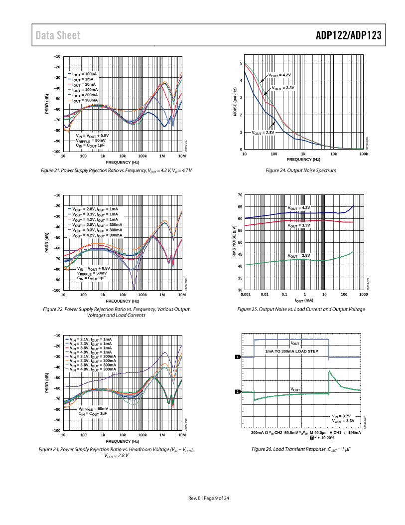
Figure 21. Power Supply Rejection Ratio vs. Frequency, VOUT = 4.2 V, VIN = 4.7 V
–100
–90
–80
–70
–60
–50
–40
–30
–20
–10
10 100 1k 10k 100k 1M 10MFREQUENCY (Hz)
PSR
R (d
B)
VOUT = 2.8V, IOUT = 1mA
VIN = VOUT + 0.5VVRIPPLE = 50mVCIN = COUT 1µF
VOUT = 3.3V, IOUT = 1mAVOUT = 4.2V, IOUT = 1mAVOUT = 2.8V, IOUT = 300mAVOUT = 3.3V, IOUT = 300mAVOUT = 4.2V, IOUT = 300mA
0839
9-01
8
Figure 22. Power Supply Rejection Ratio vs. Frequency, Various Output
Voltages and Load Currents
–100
–90
–80
–70
–60
–50
–40
–30
–20
–10
10 100 1k 10k 100k 1M 10MFREQUENCY (Hz)
PSR
R (d
B)
VIN = 3.1V, IOUT = 1mA
VRIPPLE = 50mVCIN = COUT 1µF
VIN = 3.3V, IOUT = 1mAVIN = 3.8V, IOUT = 1mAVIN = 4.8V, IOUT = 1mAVIN = 3.1V, IOUT = 300mAVIN = 3.3V, IOUT = 300mAVIN = 3.8V, IOUT = 300mAVIN = 4.8V, IOUT = 300mA
0839
9-01
9
Figure 23. Power Supply Rejection Ratio vs. Headroom Voltage (VIN − VOUT),
VOUT = 2.8 V
0
1
2
3
4
5
10 100 1k 10k 100kFREQUENCY (Hz)
NOIS
E(µ
v/√H
z)
0839
9-02
0
VOUT = 2.8V
VOUT = 3.3V
VOUT = 4.2V
Figure 24. Output Noise Spectrum
30
35
40
45
50
55
60
65
70
0.001 0.01 0.1 1 10 100 1000IOUT (mA)
RM
S N
OIS
E (µ
V)
VOUT = 4.2V
VOUT = 3.3V
VOUT = 2.8V
0839
9-02
1
Figure 25. Output Noise vs. Load Current and Output Voltage
0839
9-02
2
CH1 200mA Ω BW CH2 50.0mV B
W M 40.0µs A CH1 196mA
1
2
T 10.20%
VOUT
VIN = 3.7VVOUT = 3.3V
1mA TO 300mA LOAD STEP
IOUT
Figure 26. Load Transient Response, COUT = 1 μF
ADP122/ADP123 Data Sheet
Rev. E | Page 10 of 24
0839
9-02
3
CH1 200mA Ω BW CH2 20.0mV B
W M 40.0µs A CH1 196mA
1
2
T 10.40%
VIN = 3.7VVOUT = 3.3V
1mA TO 300mA LOAD STEP
IOUT
VOUT
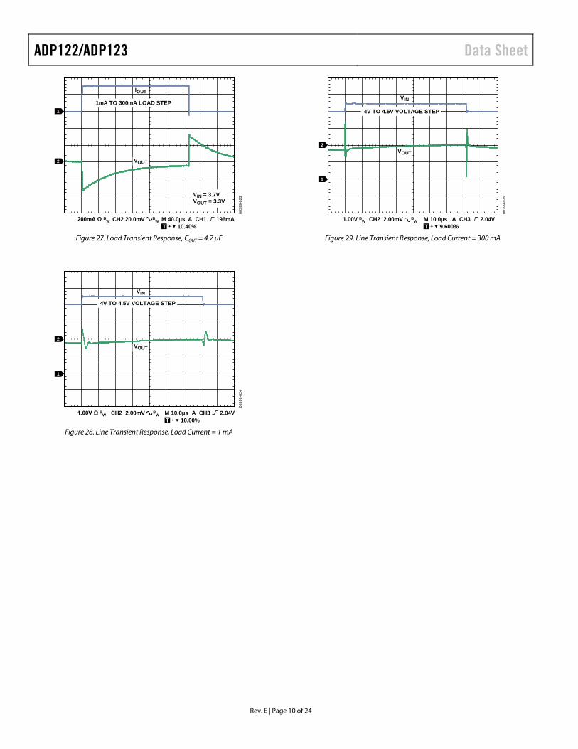
Figure 27. Load Transient Response, COUT = 4.7 μF
0839
9-02
4
CH1 1.00V Ω BW CH2 2.00mV B
W M 10.0µs A CH3 2.04V
1
2
T 10.00%
4V TO 4.5V VOLTAGE STEP
VIN
VOUT
Figure 28. Line Transient Response, Load Current = 1 mA
0839
9-02
5
CH1 1.00V BW CH2 2.00mV B
W M 10.0µs A CH3 2.04V
1
2
T 9.600%
4V TO 4.5V VOLTAGE STEP
VIN
VOUT
Figure 29. Line Transient Response, Load Current = 300 mA

Data Sheet ADP122/ADP123
Rev. E | Page 11 of 24
THEORY OF OPERATION The ADP122/ADP123 are low quiescent current, low-dropout linear regulators that operate from 2.3 V to 5.5 V and can provide up to 300 mA of output current. Drawing a low 170 µA of quies-cent current (typical) at full load makes the ADP122/ADP123 ideal for battery-operated portable equipment. Shutdown current consumption is typically 100 nA.
Optimized for use with small 1 µF ceramic capacitors, the ADP122/ADP123 provide excellent transient performance.
Internally, the ADP122/ADP123 consist of a reference, an error amplifier, a feedback voltage divider, and a PMOS pass transistor. Output current is delivered via the PMOS pass device, which is controlled by the error amplifier. The error amplifier compares the reference voltage with the feedback voltage from the output and amplifies the difference. If the feedback voltage is lower than the reference voltage, the gate of the PMOS device is pulled lower, allowing more current to pass and increasing the output voltage. If the feedback voltage is higher than the reference voltage, the gate of the PMOS device is pulled higher, allowing less current to pass and decreasing the output voltage.
The adjustable ADP123 has an output voltage range of 0.8 V to 5.0 V. The output voltage is set by the ratio of two external resistors, as shown in Figure 2. The device servos the output to maintain the voltage at the ADJ pin at 0.5 V referenced to ground. The current in R1 is then equal to 0.5 V/R2 and the current in R1 is the current in R2 plus the ADJ pin bias current. The ADJ pin bias current, 15 nA at 25°C, flows through R1 into the ADJ pin.
The output voltage can be calculated using the equation:
VOUT = 0.5 V(1 + R1/R2) + (ADJI-BIAS)(R1)
The value of R1 should be less than 200 kΩ to minimize errors in the output voltage caused by the ADJ pin bias current. For example, when R1 and R2 each equal 200 kΩ, the output voltage is 1.0 V. The output voltage error introduced by the ADJ pin bias current is 3 mV or 0.3%, assuming a typical ADJ pin bias current of 15 nA at 25°C.
Note that in shutdown, the output is turned off and the divider current is 0.
The ADP122/ADP123 use the EN pin to enable and disable the VOUT pin under normal operating conditions. When EN is high, VOUT turns on; when EN is low, VOUT turns off. For automatic startup, EN can be tied to VIN.
SHORT CIRCUIT,UVLO ANDTHERMALPROTECT
0.5V REFERENCE
ADP122
SHUTDOWN
VIN VOUT
R1
R2
GND
NOTES1. R1 AND R2 ARE INTERNAL RESISTORS, AVAILABLE ON THE ADP122 ONLY.
EN
0839
9-12
1
Figure 30. ADP122 Internal Block Diagram (Fixed Output)
SHORT CIRCUIT,UVLO ANDTHERMALPROTECT
0.5V REFERENCESHUTDOWN
VIN VOUT
GND
EN
ADJ
0839
9-12
2
ADP123
Figure 31. ADP123 Internal Block Diagram (Adjustable Output)
ADP122/ADP123 Data Sheet
Rev. E | Page 12 of 24
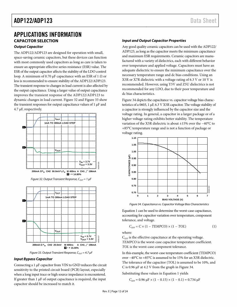
APPLICATIONS INFORMATION CAPACITOR SELECTION Output Capacitor
The ADP122/ADP123 are designed for operation with small, space-saving ceramic capacitors, but these devices can function with most commonly used capacitors as long as care is taken to ensure an appropriate effective series resistance (ESR) value. The ESR of the output capacitor affects the stability of the LDO control loop. A minimum of 0.70 µF capacitance with an ESR of 1 Ω or less is recommended to ensure stability of the ADP122/ADP123. The transient response to changes in load current is also affected by the output capacitance. Using a larger value of output capacitance improves the transient response of the ADP122/ADP123 to dynamic changes in load current. Figure 32 and Figure 33 show the transient responses for output capacitance values of 1 µF and 4.7 µF, respectively.
0839
9-02
6
CH1 200mA Ω BW CH2 50.0mV B
W M 400ns A CH1 196mA
1
2
T 14.80%
VOUT
VIN = 3.7VVOUT = 3.3V
1mA TO 300mA LOAD STEP
IOUT
Figure 32. Output Transient Response, COUT = 1 µF
0839
9-02
7
CH1 200mA Ω BW CH2 20.0mV M 400ns A CH1 196mA
1
2
T 15.00%
VOUT
VIN = 3.7VVOUT = 3.3V
1mA TO 300mA LOAD STEP
IOUT
Figure 33. Output Transient Response, COUT = 4.7 µF
Input Bypass Capacitor
Connecting a 1 µF capacitor from VIN to GND reduces the circuit sensitivity to the printed circuit board (PCB) layout, especially when a long input trace or high source impedance is encountered. If greater than 1 µF of output capacitance is required, the input capacitor should be increased to match it.
Input and Output Capacitor Properties
Any good quality ceramic capacitors can be used with the ADP122/ ADP123, as long as the capacitor meets the minimum capacitance and maximum ESR requirements. Ceramic capacitors are manu-factured with a variety of dielectrics, each with different behavior over temperature and applied voltage. Capacitors must have an adequate dielectric to ensure the minimum capacitance over the necessary temperature range and dc bias conditions. Using an X5R or X7R dielectric with a voltage rating of 6.3 V or 10 V is recommended. However, using Y5V and Z5U dielectrics is not recommended for any LDO, due to their poor temperature and dc bias characteristics.
Figure 34 depicts the capacitance vs. capacitor voltage bias charac-teristics of a 0603, 1 µF, 6.3 V X5R capacitor. The voltage stability of a capacitor is strongly influenced by the capacitor size and the voltage rating. In general, a capacitor in a larger package or of a higher voltage rating exhibits better stability. The temperature variation of the X5R dielectric is about ±15% over the −40°C to +85°C temperature range and is not a function of package or voltage rating.
0.70
0.75
0.80
0.85
0.90
0.95
1.00
1.05
1.10
0 1 2 3 4 5 6 7BIAS VOLTAGE (V)
CA
PAC
ITA
NC
E (µ
F)
0839
9-03
0
Figure 34. Capacitance vs. Capacitor Voltage Bias Characteristics
Equation 1 can be used to determine the worst-case capacitance, accounting for capacitor variation over temperature, component tolerance, and voltage.
CEFF = C × (1 − TEMPCO) × (1 − TOL) (1)
where: CEFF is the effective capacitance at the operating voltage. TEMPCO is the worst-case capacitor temperature coefficient. TOL is the worst-case component tolerance.
In this example, the worst-case temperature coefficient (TEMPCO) over −40°C to +85°C is assumed to be 15% for an X5R dielectric. The tolerance of the capacitor (TOL) is assumed to be 10%, and C is 0.96 μF at 4.2 V from the graph in Figure 34.
Substituting these values in Equation 1 yields
CEFF = 0.96 μF × (1 − 0.15) × (1 − 0.1) = 0.734 μF
Data Sheet ADP122/ADP123
Rev. E | Page 13 of 24
Therefore, the capacitor chosen in this example meets the minimum capacitance requirement of the LDO over tem-perature and tolerance at the chosen output voltage.
To guarantee the performance of the ADP122/ADP123, it is imperative that the effects of dc bias, temperature, and tolerances on the behavior of the capacitors are evaluated for each application.
UNDERVOLTAGE LOCKOUT The ADP122/ADP123 have an internal undervoltage lockout circuit that disables all inputs and the output when the input voltage is less than approximately 2 V. This ensures that the ADP122/ADP123 inputs and the output behave in a predictable manner during power-up.
ENABLE FEATURE The ADP122/ADP123 uses the EN pin to enable and disable the VOUT pin under normal operating conditions. As shown in Figure 35, when a rising voltage on EN crosses the active threshold, VOUT turns on. Conversely, when a falling voltage on EN crosses the inactive threshold, VOUT turns off.
0
0.5
1.0
1.5
2.0
2.5
3.0
3.5
0 0.2 0.4 0.6 0.8 1.0 1.2 1.4 1.6VEN
V OU
T
0839
9-23
0
Figure 35. Typical EN Pin Operation
As shown in Figure 35, the EN pin has built-in hysteresis. This prevents on/off oscillations that may occur due to noise on the EN pin as it passes through the threshold points.
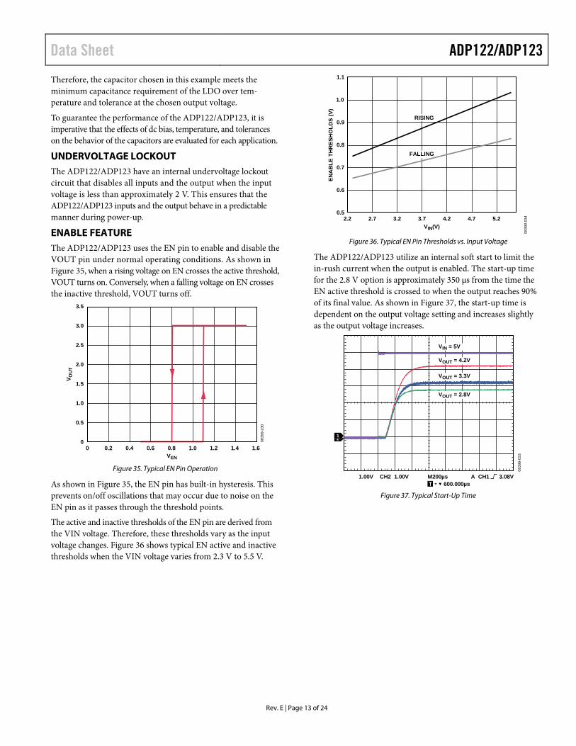
The active and inactive thresholds of the EN pin are derived from the VIN voltage. Therefore, these thresholds vary as the input voltage changes. Figure 36 shows typical EN active and inactive thresholds when the VIN voltage varies from 2.3 V to 5.5 V.
0839
9-03
4
0.5
0.6
0.7
0.8
0.9
1.0
1.1
2.2 2.7 3.2 3.7 4.2 4.7 5.2VIN(V)
ENA
BLE
TH
RES
HO
LDS
(V)
RISING
FALLING
Figure 36. Typical EN Pin Thresholds vs. Input Voltage
The ADP122/ADP123 utilize an internal soft start to limit the in-rush current when the output is enabled. The start-up time for the 2.8 V option is approximately 350 µs from the time the EN active threshold is crossed to when the output reaches 90% of its final value. As shown in Figure 37, the start-up time is dependent on the output voltage setting and increases slightly as the output voltage increases.
0839
9-03
3
CH1 1.00V CH2 1.00V M200µs A CH1 3.08V
21
T 600.000µs
VOUT = 2.8V
VOUT = 3.3V
VOUT = 4.2V
VIN = 5V
Figure 37. Typical Start-Up Time
ADP122/ADP123 Data Sheet
Rev. E | Page 14 of 24
CURRENT LIMIT AND THERMAL OVERLOAD PROTECTION The ADP122/ADP123 are protected from damage due to excessive power dissipation by current and thermal overload protection circuits. The ADP122/ADP123 are designed to limit the current when the output load reaches 500 mA (typical). When the output load exceeds 500 mA, the output voltage is reduced to maintain a constant current limit.
Thermal overload protection is included, which limits the junction temperature to a maximum of 150°C typical. Under extreme con-ditions (that is, high ambient temperature and power dissipation), when the junction temperature starts to rise above 150°C, the output is turned off, reducing output current to zero. When the junction temperature cools to less than 135°C, the output is turned on again and the output current is restored to its nominal value.
Consider the case where a hard short from VOUT to GND occurs. At first, the ADP122/ADP123 limit the current so that only 500 mA is conducted into the short. If self-heating causes the junction temperature to rise above 150°C, thermal shutdown activates, turning off the output and reducing the output current to zero. When the junction temperature cools to less than 135°C, the output turns on and conducts 500 mA into the short, again causing the junction temperature to rise above 150°C. This thermal oscillation between 135°C and 150°C results in a current oscillation between 500 mA and 0 mA that continues as long as the short remains at the output.
Current and thermal limit protections are intended to protect the device from damage due to accidental overload conditions. For reliable operation, the device power dissipation must be externally limited so that the junction temperature does not exceed 125°C.
THERMAL CONSIDERATIONS To guarantee reliable operation, the junction temperature of the ADP122/ADP123 must not exceed 125°C. To ensure that the junction temperature is less than this maximum value, the user needs to be aware of the parameters that contribute to junction temperature changes. These parameters include ambient tem-perature, power dissipation in the power device, and thermal resistances between the junction and ambient air (θJA). The value of θJA is dependent on the package assembly compounds used and the amount of copper to which the GND pins of the package are soldered on the PCB. Table 6 shows typical θJA values of the 5-lead TSOT package and 6-lead LFCSP package for various PCB copper sizes.
Table 6. Typical θJA Values for Specified PCB Copper Sizes
Copper Size (mm2) θJA (°C/W)
TSOT LFCSP 01 170 255 50 152 164
100 146 138 300 134 109 500 131 80 1 Device soldered to narrow traces.
The typical ΨJB values are 42.8°C/W for TSOT packages and 44.1°C/W for LFCSP packages.
The junction temperature of the ADP122/ADP123 can be calculated from the following equation:
TJ = TA + (PD × θJA) (2)
where: TA is the ambient temperature. PD is the power dissipation in the die, given by
PD = [(VIN − VOUT) × ILOAD] + (VIN × IGND) (3)
where: ILOAD is the load current. IGND is the ground current. VIN and VOUT are input and output voltages, respectively.
The power dissipation due to ground current is quite small and can be ignored. Therefore, the junction temperature equation can be simplified as follows:
TJ = TA + [(VIN − VOUT) × ILOAD] × θJA (4)
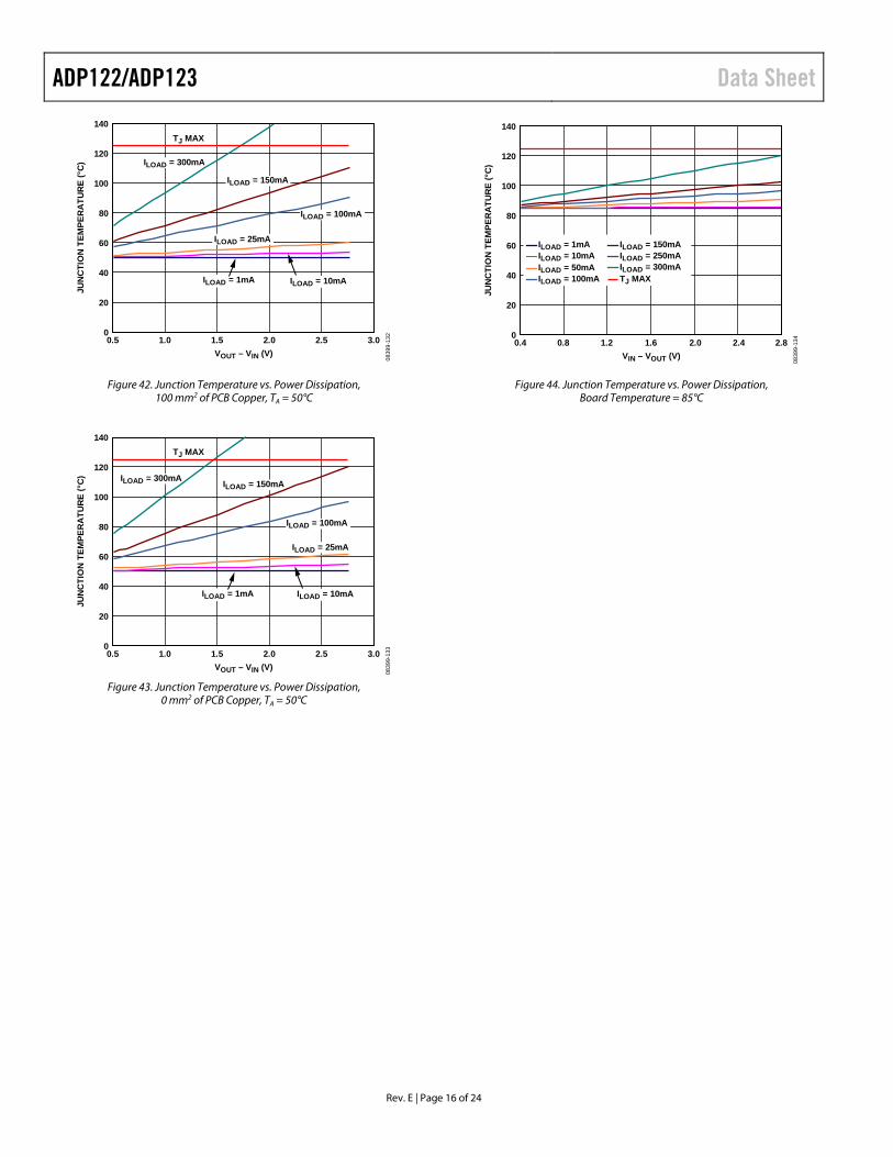
As shown in Equation 4, for a given ambient temperature, input-to-output voltage differential, and continuous load current, there exists a minimum copper size requirement for the PCB to ensure that the junction temperature does not rise above 125°C. Figure 38 through Figure 44 show junction temperature calculations for different ambient temperatures, load currents, VIN to VOUT differentials, and areas of PCB copper.
In cases where the board temperature is known, the thermal characterization parameter, ΨJB, can be used to estimate the jun-ction temperature rise. The maximum junction temperature (TJ) is calculated from the board temperature (TB) and power dissipation (PD) using the formula
TJ = TB + (PD × ΨJB) (5)

Data Sheet ADP122/ADP123
Rev. E | Page 15 of 24
JUNCTION TEMPERATURE CALCULATIONS FOR TSOT PACKAGE 140
120
100
80
60
40
20
00.5 1.0 1.5 2.0 2.5 3.0
JUN
CTI
ON
TEM
PER
ATU
RE
(°C
)
VOUT – VIN (V)
ILOAD = 1mA ILOAD = 10mA
ILOAD = 25mA
ILOAD = 100mA
ILOAD = 150mA
ILOAD = 300mA
TJ MAX
0839
9-12
8
Figure 38. Junction Temperature vs. Power Dissipation,
500 mm2 of PCB Copper, TA = 25°C
140
120
100
80
60
40
20
0
JUN
CTI
ON
TEM
PER
ATU
RE
(°C
)
VOUT – VIN (V)
ILOAD = 1mA ILOAD = 10mA
ILOAD = 25mA
ILOAD = 100mA
ILOAD = 150mA
ILOAD = 300mA
TJ MAX
0.5 1.0 1.5 2.0 2.5 3.0
0839
9-12
9
Figure 39. Junction Temperature vs. Power Dissipation,
100 mm2 of PCB Copper, TA = 25°C
140
120
100
80
60
40
20
0
JUN
CTI
ON
TEM
PER
ATU
RE
(°C
)
VOUT – VIN (V)
ILOAD = 1mA ILOAD = 10mA
ILOAD = 25mA
ILOAD = 100mA
ILOAD = 150mA
ILOAD = 300mA
TJ MAX
0.5 1.0 1.5 2.0 2.5 3.0
0839
9-13
0
Figure 40. Junction Temperature vs. Power Dissipation,
0 mm2 of PCB Copper, TA = 25°C
140
120
100
80
60
40
20
0
JUN
CTI
ON
TEM
PER
ATU
RE
(°C
)
VOUT – VIN (V)
ILOAD = 1mA ILOAD = 10mA
ILOAD = 25mA
ILOAD = 100mA
ILOAD = 150mAILOAD = 300mA
TJ MAX
0.5 1.0 1.5 2.0 2.5 3.0
0839
9-13
1
Figure 41. Junction Temperature vs. Power Dissipation,
500 mm2 of PCB Copper, TA = 50°C
ADP122/ADP123 Data Sheet
Rev. E | Page 16 of 24
140
120
100
80
60
40
20
0
JUN
CTI
ON
TEM
PER
ATU
RE
(°C
)
VOUT – VIN (V)
ILOAD = 1mA
ILOAD = 25mA
ILOAD = 100mA
ILOAD = 150mA
ILOAD = 300mA
TJ MAX
ILOAD = 10mA
0.5 1.0 1.5 2.0 2.5 3.0
0839
9-13
2
Figure 42. Junction Temperature vs. Power Dissipation, 100 mm2 of PCB Copper, TA = 50°C
140
120
100
80
60
40
20
0
JUN
CTI
ON
TEM
PER
ATU
RE
(°C
)
VOUT – VIN (V)
ILOAD = 1mA
ILOAD = 25mA
ILOAD = 100mA
ILOAD = 150mAILOAD = 300mA
TJ MAX
ILOAD = 10mA
0.5 1.0 1.5 2.0 2.5 3.0
0839
9-13
3
Figure 43. Junction Temperature vs. Power Dissipation,
0 mm2 of PCB Copper, TA = 50°C
140
120
100
80
60
40
20
0
JUN
CTI
ON
TEM
PER
ATU
RE
(°C
)
VIN – VOUT (V)
ILOAD = 1mAILOAD = 10mAILOAD = 50mAILOAD = 100mA
ILOAD = 150mAILOAD = 250mAILOAD = 300mATJ MAX
0.4 0.8 1.2 1.6 2.0 2.4 2.8
0839
9-13
4
Figure 44. Junction Temperature vs. Power Dissipation, Board Temperature = 85°C
Data Sheet ADP122/ADP123
Rev. E | Page 17 of 24
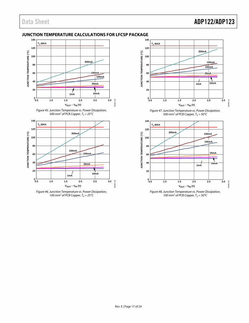
JUNCTION TEMPERATURE CALCULATIONS FOR LFCSP PACKAGE
0
20
40
60
80
100
120
140
0.5 1.0 1.5 2.0 2.5 3.0
JUN
CTI
ON
TEM
PER
ATU
RE
(°C
)
TJ MAX
VOUT – VIN (V)
0839
9-13
9
25mA
100mA150mA
300mA
1mA 10mA
Figure 45. Junction Temperature vs. Power Dissipation,
500 mm2 of PCB Copper, TA = 25°C
0
20
40
60
80
100
120
140
0.5 1.0 1.5 2.0 2.5 3.0
JUN
CTI
ON
TEM
PER
ATU
RE
(°C
)
TJ MAX
VOUT – VIN (V)
0839
9-14
0
25mA
100mA150mA
300mA
1mA10mA
Figure 46. Junction Temperature vs. Power Dissipation,
100 mm2 of PCB Copper, TA = 25°C
3.00
20
40
60
80
100
120
140
0.5 1.0 1.5 2.0 2.5
JUN
CTI
ON
TEM
PER
ATU
RE
(°C
)
TJ MAX
VOUT – VIN (V)
0839
9-14
1
25mA
100mA
150mA
300mA
1mA 10mA
Figure 47. Junction Temperature vs. Power Dissipation,
500 mm2 of PCB Copper, TA = 50°C
0
20
60
80
100
120
140
0.5 1.0 1.5 2.0 2.5 3.0
JUN
CTI
ON
TEM
PER
ATU
RE
(°C
)
TJ MAX
VOUT – VIN (V)
0839
9-14
2
25mA
100mA
150mA300mA
1mA10mA40
Figure 48. Junction Temperature vs. Power Dissipation,
100 mm2 of PCB Copper, TA = 50°C

ADP122/ADP123 Data Sheet
Rev. E | Page 18 of 24
150mA
0
20
40
60
80
100
120
140
0.5 1.0 1.5 2.0 2.5 3.0
JUN
CTI
ON
TEM
PER
ATU
RE
(°C
)
VOUT – VIN (V)
TJ MAX
0839
9-14
3
25mA
100mA
300mA
1mA10mA
Figure 49. Junction Temperature vs. Power Dissipation,
0 mm2 of PCB Copper, TA = 25°C
0
20
40
60
80
100
120
140
0.5 1.0 1.5 2.0 2.5 3.0
JUN
CTI
ON
TEM
PER
ATU
RE
(°C
)
VOUT – VIN (V)
TJ MAX
0839
9-14
5
25mA
100mA
150mA300mA
1mA10mA
Figure 50. Junction Temperature vs. Power Dissipation,
0 mm2 of PCB Copper, TA = 50°C
0
20
40
60
80
100
120
140
0.4 0.8 1.2 1.6 2.0 2.4 2.8
JUN
CTI
ON
TEM
PER
ATU
RE
(°C
)
VOUT – VIN (V)
25mA
100mA
150mA300mA
TJ MAX
1mA 10mA
0839
9-14
4
Figure 51. Junction Temperature vs. Power Dissipation,
Board Temperature = 85°C
Data Sheet ADP122/ADP123
Rev. E | Page 19 of 24
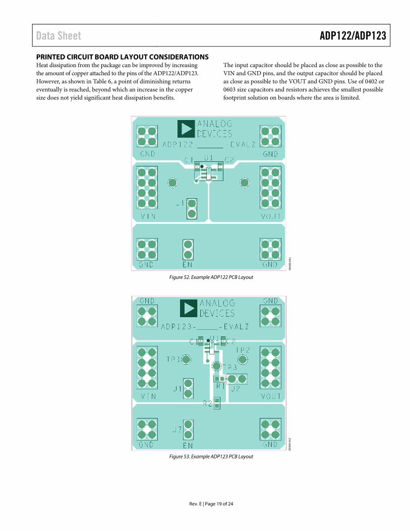
PRINTED CIRCUIT BOARD LAYOUT CONSIDERATIONS Heat dissipation from the package can be improved by increasing the amount of copper attached to the pins of the ADP122/ADP123. However, as shown in Table 6, a point of diminishing returns eventually is reached, beyond which an increase in the copper size does not yield significant heat dissipation benefits.
The input capacitor should be placed as close as possible to the VIN and GND pins, and the output capacitor should be placed as close as possible to the VOUT and GND pins. Use of 0402 or 0603 size capacitors and resistors achieves the smallest possible footprint solution on boards where the area is limited.
0839
9-04
1
Figure 52. Example ADP122 PCB Layout
08
399-
042
Figure 53. Example ADP123 PCB Layout
ADP122/ADP123 Data Sheet
Rev. E | Page 20 of 24
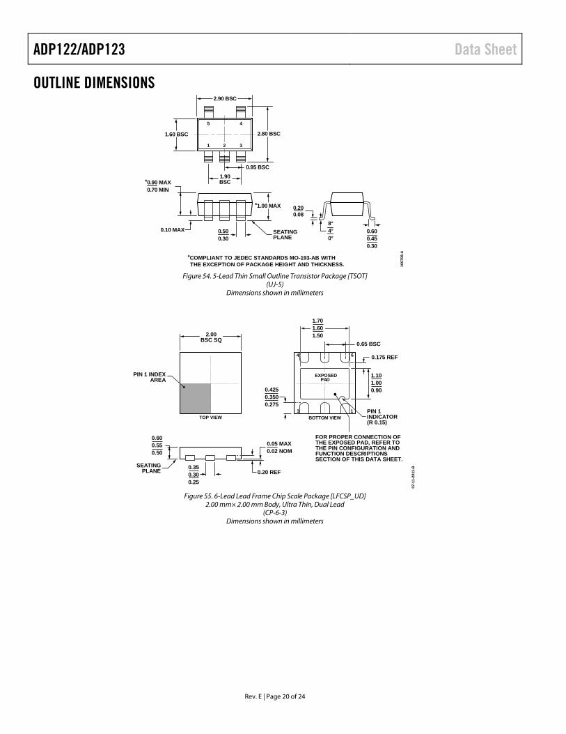
OUTLINE DIMENSIONS
1007
08-A
*COMPLIANT TO JEDEC STANDARDS MO-193-AB WITHTHE EXCEPTION OF PACKAGE HEIGHT AND THICKNESS.
1.60 BSC 2.80 BSC
1.90BSC
0.95 BSC
0.200.08
0.600.450.30
8°4°0°
0.500.30
0.10 MAX
*1.00 MAX
*0.90 MAX0.70 MIN
2.90 BSC
5 4
1 2 3
SEATINGPLANE
Figure 54. 5-Lead Thin Small Outline Transistor Package [TSOT]
(UJ-5) Dimensions shown in millimeters
1.701.601.50
0.4250.3500.275
TOP VIEW
6
1
4
3
0.350.300.25
BOTTOM VIEW
PIN 1 INDEXAREA
SEATINGPLANE
0.600.550.50
1.101.000.90
0.20 REF
0.05 MAX0.02 NOM
2.00BSC SQ
0.65 BSC
EXPOSEDPAD
PIN 1INDICATOR(R 0.15)
FOR PROPER CONNECTION OFTHE EXPOSED PAD, REFER TOTHE PIN CONFIGURATION ANDFUNCTION DESCRIPTIONSSECTION OF THIS DATA SHEET.
07-1
1-20
11-B
0.175 REF
Figure 55. 6-Lead Lead Frame Chip Scale Package [LFCSP_UD]
2.00 mm× 2.00 mm Body, Ultra Thin, Dual Lead (CP-6-3)
Dimensions shown in millimeters
Data Sheet ADP122/ADP123
Rev. E | Page 21 of 24
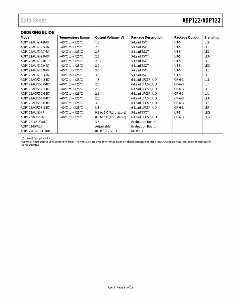
ORDERING GUIDE Model1 Temperature Range Output Voltage (V)2 Package Description Package Option Branding ADP122AUJZ-1.8-R7 –40°C to +125°C 1.8 5-Lead TSOT UJ-5 LJS ADP122AUJZ-2.5-R7 –40°C to +125°C 2.5 5-Lead TSOT UJ-5 LE6 ADP122AUJZ-2.7-R7 –40°C to +125°C 2.7 5-Lead TSOT UJ-5 LE9 ADP122AUJZ-2.8-R7 –40°C to +125°C 2.8 5-Lead TSOT UJ-5 LEA ADP122AUJZ-2.85-R7 –40°C to +125°C 2.85 5-Lead TSOT UJ-5 LEC ADP122AUJZ-2.9-R7 –40°C to +125°C 2.9 5-Lead TSOT UJ-5 LED ADP122AUJZ-3.0-R7 –40°C to +125°C 3.0 5-Lead TSOT UJ-5 LEE ADP122AUJZ-3.3-R7 –40°C to +125°C 3.3 5-Lead TSOT UJ-5 LEF ADP122ACPZ-1.8-R7 –40°C to +125°C 1.8 6-Lead LFCSP_UD CP-6-3 LJS ADP122ACPZ-2.0-R7 –40°C to +125°C 2.0 6-Lead LFCSP_UD CP-6-3 LJT ADP122ACPZ-2.5-R7 –40°C to +125°C 2.5 6-Lead LFCSP_UD CP-6-3 LE6 ADP122ACPZ-2.6-R7 –40°C to +125°C 2.6 6-Lead LFCSP_UD CP-6-3 LJU ADP122ACPZ-2.8-R7 –40°C to +125°C 2.8 6-Lead LFCSP_UD CP-6-3 LEA ADP122ACPZ-3.0-R7 –40°C to +125°C 3.0 6-Lead LFCSP_UD CP-6-3 LEE ADP122ACPZ-3.3-R7 –40°C to +125°C 3.3 6-Lead LFCSP_UD CP-6-3 LEF ADP123AUJZ-R7 –40°C to +125°C 0.8 to 5.0 (Adjustable) 5-Lead TSOT UJ-5 LEG ADP123ACPZ-R7 –40°C to +125°C 0.8 to 5.0 (Adjustable) 6-Lead LFCSP_UD CP-6-3 LEG ADP122-3.3-EVALZ 3.3 Evaluation Board ADP123-EVALZ Adjustable Evaluation Board ADP122UJZ-REDYKIT REDYKIT 2.5,3.3 REDYKIT 1 Z = RoHS Compliant Part. 2 Up to 31 fixed-output voltage options from 1.75 V to 3.3 V are available. For additional voltage options, contact a local Analog Devices, Inc., sales or distribution
representative.

ADP122/ADP123 Data Sheet
Rev. E | Page 22 of 24
NOTES

Data Sheet ADP122/ADP123
Rev. E | Page 23 of 24
NOTES

ADP122/ADP123 Data Sheet
Rev. E | Page 24 of 24
NOTES
©2009–2012 Analog Devices, Inc. All rights reserved. Trademarks and registered trademarks are the property of their respective owners. D08399-0-6/12(E)