Embed Size (px)
Citation preview

50 dB GSM PA Controller AD8311
Rev. A Information furnished by Analog Devices is believed to be accurate and reliable. However, no responsibility is assumed by Analog Devices for its use, nor for any infringements of patents or other rights of third parties that may result from its use. Specifications subject to change without notice. No license is granted by implication or otherwise under any patent or patent rights of Analog Devices. Trademarks and registered trademarks are the property of their respective owners.
One Technology Way, P.O. Box 9106, Norwood, MA 02062-9106, U.S.A.Tel: 781.329.4700 www.analog.com Fax: 781.461.3113 ©2005–2011 Analog Devices, Inc. All rights reserved.
FEATURES Complete RF detector/controller function >50 dB range at 0.9 GHz (−48 dBm to +3 dBm re 50 Ω) Accurate scaling from 0.1 GHz to 2.5 GHz Temperature-stable linear-in-dB response Log slope of 23 mV/dB, intercept at −60 dBm at 0.9 GHz True integration function in control loop Low power: 20 mW at 2.7 V
APPLICATIONS Single, dual, and triple band mobile handset (GSM, DCS,
EDGE) Transmitter power control
GENERAL DESCRIPTION
The AD8311 is a complete low cost subsystem for the precise control of RF power amplifiers operating in the frequency range 0.1 GHz to 2.5 GHz and over a typical dynamic range of 50 dB. It is intended for use in cellular handsets and other battery-operated wireless devices. The log amp technique provides a much wider measurement range and better accuracy than controllers using diode detectors. In particular, its temperature stability is excellent over a specified range of −40°C to +85°C.
Its high sensitivity allows control at low signal levels, thus reducing the amount of power that needs to be coupled to the detector. For convenience, the signal is internally ac-coupled. This high-pass coupling, with a corner at approximately 0.016 GHz, determines the lowest operating frequency. Thus, the source can be dc-grounded.
The AD8311 provides a voltage output, VAPC, which has the voltage range and current drive to directly connect to the gain control pin of most handset power amplifiers. VAPC can swing from 300 mV above ground to within 200 mV below the supply voltage. Load currents of up to 6 mA can be supported.
The setpoint control input is applied to pin VSET and has an operating range of 0.25 V to 1.4 V. The associated circuit determines the slope and intercept of the linear-in-dB measurement system; these are nominally 23.6 mV/dB and −59.7 dBm at 0.9 GHz. Further simplifying the application of the AD8311, the input resistance of the setpoint interface is over 35 MΩ, and the bias current is typically 0.26 μA.
The AD8311 is available in a 6-ball wafer-level chip scale package (WLCSP), 1.0 mm × 1.5 mm, and consumes 7.6 mA from a 2.7 V to 5.5 V supply.
FUNCTIONAL BLOCK DIAGRAM
10dB
OFFSETCOMPENSATION
INTERCEPTPOSITIONING
10dB10dB10dB
DETDETDETDETDET
RFIN
⋅ 1.35HI-Z
LOW NOISERAIL-TO-RAIL BUFFER
VSET23mV/dB250mV TO1.4V = 50dB
FLTR
VAPC
LOW NOISEBAND GAP
REFERENCE
LOW NOISEGAIN BIAS
COMM
VPOS
V I
0554
5-00
1
Figure 1.
AD8311
Rev. A | Page 2 of 24
TABLE OF CONTENTS Specifications..................................................................................... 3
Absolute Maximum Ratings............................................................ 5
ESD Caution.................................................................................. 5
Pin Configuration and Function Descriptions............................. 6
Typical Performance Characteristics ............................................. 7
Theory of Operation ...................................................................... 11
Basic Theory................................................................................ 11
Controller-Mode Log Amps ..................................................... 12
Control Loop Dynamics............................................................ 12
Basic Connections ...................................................................... 14
Range on VSET and RFIN......................................................... 14
Transient Response..................................................................... 15
Mobile Handset Power Control Example ............................... 15
Power-On and Power-Off ......................................................... 16
Input Coupling Options ............................................................ 16
Temperature Drift ...................................................................... 17
Device Calibration and Error Calculation.............................. 17
Selecting Calibration Points to Improve Accuracy over a Reduced Range ........................................................................... 18
Device Handling......................................................................... 19
Evaluation Board ............................................................................ 20
Outline Dimensions ....................................................................... 22
Ordering Guide .......................................................................... 22
REVISION HISTORY
1/11—Rev. 0 to Rev. A Updated Outline Dimensions ....................................................... 22 Changes to Ordering Guide .......................................................... 22 6/05—Revision 0: Initial Version

AD8311
Rev. A | Page 3 of 24
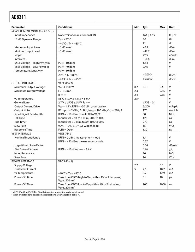
SPECIFICATIONS VPOS = 2.7 V, Frequency = 0.1 GHz, TA = 25°C, 52.3 Ω termination on RFIN, light condition = 600 lux, unless otherwise noted.
Table 1. Parameter Conditions Min Typ Max Unit SPECIFIED FREQUENCY RANGE RFIN (Pin 6) 0.1 2.5 GHz MEASUREMENT MODE1 (f = 0.1 GHz)
Input Impedance No termination resistor on RFIN 2140 || 1.97 Ω || pF
1 dB Dynamic Range TA = +25°C 47 dB
−40°C < TA < +85°C 46 dB Maximum Input Level ±1 dB error +2 +2.6 dBm Minimum Input Level ±1 dB error −44.5 −44 dBm Slope2 21.5 23.8 25.5 mV/dB Intercept2 −66 −58.9 −51 dBm VSET Voltage—High Power In PIN = –10 dBm 1.16 V VSET Voltage—Low Power In PIN = –40 dBm 0.45 V Temperature Sensitivity PIN = –10 dBm 25C ≤ TA ≤ +85C −0.0020 dB/°C
−40C ≤ TA ≤ +25°C +0.0121 dB/°C
MEASUREMENT MODE (f = 0.9 GHz) Input Impedance No termination resistor on RFIN 370 || 1.58 Ω || pF
1 dB Dynamic Range TA = +25C 51 dB
−40C < TA < +85C 50 dB
Maximum Input Level ±1 dB error +2.8 dBm Minimum Input Level ±1 dB error −47.9 dBm Slope2 23.6 mV/dB Intercept2 −59.7 dBm VSET Voltage—High Power In PIN = –10 dBm 1.17 V VSET Voltage—Low Power In PIN = –40 dBm 0.46 V Temperature Sensitivity PIN = –10 dBm
25C ≤ TA ≤ +85C 0.0015 dB/°C
−40C ≤ TA ≤ +25C 0.0094 dB/°C
MEASUREMENT MODE (f = 1.9 GHz) Input Impedance No termination resistor on RFIN 180 || 1.67 Ω || pF
1 dB Dynamic Range TA = +25°C 42 dB
−40°C < TA < +85°C 41 dB Maximum Input Level ±1 dB error −5.6 dBm Minimum Input Level ±1 dB error −48.0 dBm Slope2 22.7 mV/dB Intercept2 −60.8 dBm VSET Voltage—High Power In PIN = –10 dBm 1.15 V VSET Voltage—Low Power In PIN = –40 dBm 0.47 V Temperature Sensitivity PIN = –10 dBm
25°C ≤ TA ≤ +85°C 0.0056 dB/°C −40°C ≤ TA ≤ +25°C 0.0077 dB/°C
AD8311
Rev. A | Page 4 of 24
Parameter Conditions Min Typ Max Unit MEASUREMENT MODE (f = 2.5 GHz)
Input Impedance No termination resistor on RFIN 164 || 1.55 Ω || pF
±1 dB Dynamic Range TA = +25°C 42 dB
−40°C < TA < +85°C 41 dB
Maximum Input Level ±1 dB error −6.2 dBm Minimum Input Level ±1 dB error −47.7 dBm Slope2 22.5 mV/dB Intercept2 −60.6 dBm VSET Voltage—High Power In PIN = –10 dBm 1.14 V VSET Voltage—Low Power In PIN = –40 dBm 0.46 V Temperature Sensitivity PIN = –10 dBm 25°C ≤ TA ≤ 85°C −0.0004 dB/°C −40°C ≤ TA ≤ +25°C +0.0090 dB/°C
OUTPUT INTERFACE VAPC (Pin 2) Minimum Output Voltage VSET ≤ 150mV 0.2 0.3 0.4 V Maximum Output Voltage IOUT = 3 mA 2.3 2.55 V RL = ∞ 2.4 2.65 V vs. Temperature 85°C, VPOS = 3 V, IOUT = 6 mA 2.54 V General Limit 2.7 V ≤ VPOS ≤ 5.5 V, RL = ∞ VPOS – 0.1 V Output Current Drive VSET = 1.5 V, RFIN = –50 dBm, source/sink 5/200 mA/μA Output Noise RF Input = 2 GHz, 0 dBm, fNOISE = 100 kHz, CFLT = 220 pF 170 nV/√Hz Small Signal Bandwidth RFIN = −10 dBm; from FLTR to VAPC 30 MHz Fall Time Input level = off to 0 dBm, 90% to 10% 120 ns Rise Time Input level = 0 dBm to off, 10% to 90% 270 ns Slew Rate 90% – 10%, VSET = 0.3 V, open loop 15 V/μs Response Time FLTR = Open 130 ns
VSET INTERFACE VSET (Pin 3) Nominal Input Range RFIN = 0 dBm; measurement mode 1.4 V RFIN = −50 dBm; measurement mode 0.27 V Logarithmic Scale Factor 0.04 dB/mV Bias Current Source RFIN = −10 dBm; VSET = 1.4 V 0.26 μA Input Resistance 36 MΩ Slew Rate 14 V/μs
POWER INTERFACE VPOS (Pin 1) Supply Voltage 2.7 5.5 V Quiescent Current 5 7.6 10.7 mA vs. Temperature –40°C ≤ TA ≤ +85°C 8.2 12.9 mA
Power-On Time Time from VPOS high to VAPC within 1% of final value, VSET ≤ 200 mV
3 10 μs
Power-Off Time Time from VPOS low to VAPC within 1% of final value, VSET ≤ 200 mV
100 2000 ns
1 VAPC (Pin 2) to VSET (Pin 3) with inversion stage, sinusoidal input signal. 2 Mean and standard deviation specifications are available in . Table 4

AD8311
Rev. A | Page 5 of 24
ABSOLUTE MAXIMUM RATINGS Table 2. Parameters Ratings Supply Voltage VPOS 5.5 V VAPC, VSET 0 V, VPOS RFIN 17 dBm Equivalent Voltage 1.6 V rms Internal Power Dissipation 60 mW θJA (WLCSP) 200°C/W Maximum Junction Temperature 125°C Operating Temperature Range −40°C to +85°C Storage Temperature Range −65°C to +150°C
Stresses above those listed under Absolute Maximum Ratings may cause permanent damage to the device. This is a stress rating only; functional operation of the device at these or any other conditions above those indicated in the operational section of this specification is not implied. Exposure to absolute maximum rating conditions for extended periods may affect device reliability.
ESD CAUTION

AD8311
Rev. A | Page 6 of 24
PIN CONFIGURATION AND FUNCTION DESCRIPTIONS
VPOS RFIN
VAPC
VSET FLTR
TOP VIEWNot to Scale 05
545-
002
1
2
3
BUMP 1INDICATOR
COMM
6
5
4
Figure 2. Pin Configuration
Table 3. Pin Function Descriptions Pin No. Mnemonic Function 1 VPOS Positive Supply Voltage: 2.7 V to 5.5 V. 2 VAPC Output. Control voltage for gain control element. 3 VSET Setpoint Input. Nominal input range 0.25 V to 1.4 V. 4 FLTR Integrator Capacitor. Connect between FLTR and COMM. 5 COMM Device Common (Ground). 6 RFIN RF Input.

AD8311
Rev. A | Page 7 of 24
TYPICAL PERFORMANCE CHARACTERISTICS VPOS = 2.7 V; TA = 25°C; CFLT = open; light condition = 600 lux, 52.3 Ω termination; unless otherwise noted. Colors: +25°C = black, −40°C = blue, +85°C = red.
10
–600.2 1.6
0554
5-01
7
VSET (V)
RF
INPU
T A
MPL
ITU
DE
(dB
m)
0
–10
–20
–30
–40
–50
0.4 0.6 0.8 1.0 1.2 1.4
0.1GHz
0.9GHz1.9GHz2.5GHz
Figure 3. Input Amplitude vs. VSET
10
–600.2 1.6
0554
5-01
8
VSET (V)
RF
INPU
T A
MPL
ITU
DE
(dB
m)
0
–10
–20
–30
–40
–50
0.4 0.6 0.8 1.0 1.2 1.4
4
–3
3
2
1
0
–1
–2
ERR
OR
(dB
)
+85°C
–40°C+25°C
+85°C
–40°C
+25°CERROR AT +85°C AND –40°CBASED ON DEVIATION FROMSLOPE AND INTERCEPT AT +25°C
Figure 4. Input Amplitude and Log Conformance vs. VSET at 0.1 GHz
−40°C, +25°C, and +85°C
10
–600.2 1.6
0554
5-01
9
VSET (V)
RF
INPU
T A
MPL
ITU
DE
(dB
m)
0
–10
–20
–30
–40
–50
0.4 0.6 0.8 1.0 1.2 1.4
4
–3
3
2
1
0
–1
–2
ERR
OR
(dB
)
ERROR AT +85°C AND –40°CBASED ON DEVIATION FROMSLOPE AND INTERCEPT AT +25°C
+85°C
+85°C
–40°C+25°C
–40°C+25°C
Figure 5. Input Amplitude and Log Conformance vs. VSET at 0.9 GHz
−40°C, +25°C, and +85°C
4
–30.2 1.6
0554
5-02
0
VSET (V)
ERR
OR
(dB
)
3
2
1
0
–1
–2
0.4 0.6 0.8 1.0 1.2 1.4
0.1GHz2.5GHz
1.9GHz
0.9GHz
Figure 6. Log Conformance vs. VSET
10
–600.2 1.6
0554
5-02
1
VSET (V)
RF
INPU
T A
MPL
ITU
DE
(dB
m)
0
–10
–20
–30
–40
–50
0.4 0.6 0.8 1.0 1.2 1.4
4
–3
3
2
1
0
–1
–2
ERR
OR
(dB
)
+85°C
–40°C+25°C
+85°C
–40°C
+25°C
ERROR AT +85°C AND –40°CBASED ON DEVIATION FROMSLOPE AND INTERCEPT AT +25°C
Figure 7. Input Amplitude and Log Conformance vs. VSET at 1.9 GHz
−40°C, +25°C, and +85°C
10
–600.2 1.6
0554
5-02
2
VSET (V)
RF
INPU
T A
MPL
ITU
DE
(dB
m)
0
–10
–20
–30
–40
–50
0.4 0.6 0.8 1.0 1.2 1.4
4
–3
3
2
1
0
–1
–2
ERR
OR
(dB
)+85°C
–40°C+25°C
+85°C–40°C+25°C
ERROR AT +85°C AND –40°CBASED ON DEVIATION FROMSLOPE AND INTERCEPT AT +25°C
Figure 8. Input Amplitude and Log Conformance vs. VSET at 2.5 GHz
−40°C, +25°C, and +85°C

AD8311
Rev. A | Page 8 of 24
3
–3–60 10
0554
5-02
3
RF INPUT AMPLITUDE (dBm)
ERR
OR
(dB
)
2
1
0
–1
–2
–50 –40 –30 –20 –10 0
–40°C
+85°C
+25°C
Figure 9. Distribution of Error over Temperature After Ambient Normalization vs. Input Amplitude at 0.1 GHz
3
–3–60 10
0554
5-02
4
RF INPUT AMPLITUDE (dBm)
ERR
OR
(dB
)
2
1
0
–1
–2
–50 –40 –30 –20 –10 0
–40°C
+85°C
+25°C
Figure 10. Distribution of Error over Temperature after Ambient Normalization vs. Input Amplitude at 0.9 GHz
3.5
2.32.7 3.5
0554
5-02
5
VPOS (V)
V APC
(V)
3.3
3.1
2.9
2.7
2.5
2.8 2.9 3.0 3.1 3.2 3.3 3.4
0mA
2mA 4mA
6mA
Figure 11. Maximum VAPC Voltage vs. Supply Voltage by Load Current
3
–3–60 10
0554
5-02
6
RF INPUT AMPLITUDE (dBm)
ERR
OR
(dB
)
2
1
0
–1
–2
–50 –40 –30 –20 –10 0
–40°C
+85°C
+25°C
Figure 12. Distribution of Error over Temperature After Ambient Normalization vs. Input Amplitude at 1.9 GHz
3
–3–60 10
0554
5-02
7
RF INPUT AMPLITUDE (dBm)
ERR
OR
(dB
)
2
1
0
–1
–2
–50 –40 –30 –20 –10 0
–40°C
+85°C
+25°C
Figure 13. Distribution of Error over Temperature after Ambient Normalization vs. Input Amplitude at 2.5 GHz
100MHz
900MHz
1.9GHz2.5GHz
START FREQUENCY = 0.05GHzSTOP FREQUENCY = 3.5GHz
0554
5-02
8
Figure 14. Input Impedance vs. Frequency, No Termination Resistor on RFIN

AD8311
Rev. A | Page 9 of 24
0554
5-02
9GND
GND
200mV PERVERTICALDIVISION
VAPC
1V PERVERTICALDIVISION
2μs PERHORIZONTALDIVISION
VPOS
Figure 15. Power-On and -Off Response with VSET Grounded
TEK TDS694CSCOPE
TRIGTEK P6205FET PROBE
VPOS
VAPC
VSET
RFIN
COMM
FLTR
AD83111
2
3 4
5
6
220pF
52.3Ω
STANFORD DS345PULSE
GENERATOR
PULSE OUT
TRIGOUTR AND S SMT03
SIGNALGENERATOR
RF OUT
10MHz REFOUTPUT EXTTRIG
AD811
TEK P6205FET PROBE
49.9Ω
732Ω
0554
5-03
0
Figure 16. Test Setup for Power-On and -Off Response with VSET Grounded
FREQUENCY (Hz)
45
10
AM
PLIT
UD
E (d
B)
35
25
15
5
–5
–15
–25
–35
100 1k 10k 100k 1M 10M
0
–20
–40
–60
–80
–100
–120
PHA
SE (D
egre
es)
40
20
0
–20
30
10
–10
–30
–40
–10
–30
–50
–70
–90
–110
–130CFLT = 220pF
CFLT = 0pF
0554
5-03
9
Figure 17. AC Response from VSET to VAPC
0554
5-03
2
GND
GND
1V PERVERTICALDIVISION
VAPC
RFINPUT
PULSED RF0.1GHz, 0dBm 100ns PER
HORIZONTALDIVISION
Figure 18. VAPC Response Time, Full-Scale Amplitude Change, Open-Loop
VPOS
VAPC
VSET
RFIN
COMM
FLTR
AD83111
2
3 4
5
6
2.7V
0.1μF
TEK P6205FET PROBE
TEK TDS694CSCOPE
TRIG
PICOSECONDPULSE LABS
PULSEGENERATOR
TRIGOUT
R AND S SMT03SIGNAL
GENERATORPULSE
MODULATIONMODE
10MHz REFOUTPUT EXT TRIG
PULSE MODE IN OUT
RF OUT
–3dB–3dB
0.3V
RFSPLITTER
52.3Ω
NC
NC = NO CONNECT
0554
5-03
3
Figure 19. Test Setup for VAPC Response Time
10k
10100 10M
0554
5-03
4
FREQUENCY (Hz)
NO
ISE
SPEC
TRA
L D
ENSI
TY (n
V/ H
z)
100
1k
1k 10k 100k 1M
–35dBm0dBm
–20dBm –10dBm–30dBm
–38dBm
–40dBm
–50dBm
CFLT = 220pF, RF INPUT = 2GHz
Figure 20. VAPC Noise Spectral Density

AD8311
Rev. A | Page 10 of 24
25
210 2.5
0554
5-03
5
FREQUENCY (GHz)
SLO
PE (m
V/dB
)
23
23
22
0.5 1.0 1.5 2.0
+25°C
–40°C
+85°C
Figure 21. Slope vs. Frequency −40°C, +25°C, and +85°C
25
21 0554
5-03
6
VPOS (V)
SLO
PE (m
V/dB
)
23
23
22
2.5 5.53.0 3.5 4.0 4.5 5.0
0.1GHz
0.9GHz
1.9GHz
2.5GHz
Figure 22. Slope vs. Supply Voltage
–55
–650 2.5
0554
5-03
7
FREQUENCY (GHz)
INTE
RC
EPT
(dB
m)
–57
–61
–63
0.5 1.0 1.5 2.0
–59+25°C
–40°C+85°C
Figure 23. Intercept vs. Frequency
−40°C, +25°C, and +85°C
–58
–632.5 5.5
0554
5-03
8
VPOS (V)
INTE
RC
EPT
(dB
m)
–59
–61
–62
3.0 3.5 4.0 4.5
–60
5.0
0.1GHz
0.9GHz
1.9GHz
2.5GHz
Figure 24. Intercept vs. Supply Voltage
Table 4. Typical Specifications at Selected Frequencies at 25°C (Mean and Sigma) ±1 dB Dynamic Range Slope (mV/dB) Intercept (dBm) Low Point (dBm) High Point (dBm) Frequency (GHz) Mean Sigma Mean Sigma Mean Sigma Mean Sigma 0.1 23.8 0.1 −58.9 0.4 −44.5 0.8 +2.6 0.3 0.9 23.6 0.1 −59.7 0.4 −47.9 0.3 +2.8 0.1 1.9 22.7 0.1 −60.8 0.5 −48.0 0.6 −5.6 0.6 2.5 22.5 0.1 −60.6 0.5 −47.7 0.6 −6.2 0.5

AD8311
Rev. A | Page 11 of 24
THEORY OF OPERATION The AD8311 is a wideband logarithmic amplifier (log amp) similar in design to the AD8313, AD8314, and AD8315. Like the AD8315, it is strictly optimized for use in power control applications rather than as a measurement device. Figure 25 shows the main features in block schematic form. The output (Pin 2, VAPC) is intended to be applied directly to the automatic power-control (APC) pin of a power amplifier module.
BASIC THEORY Logarithmic amplifiers provide a type of compression in which a signal having a large range of amplitudes is converted to one of a smaller range. The use of the logarithmic function uniquely results in the output representing the decibel value of the input. The fundamental mathematical form is
Z
INSLPOUT V
VVV 10log= (1)
where:
VIN is the input voltage. VZ is called the intercept (voltage) because when VIN = VZ the
argument of the logarithm is unity and thus the result is zero. VSLP is called the slope (voltage), which is the amount by which
the output changes for a certain change in the ratio (VIN/VZ).
When BASE-10 logarithms are used, denoted by the function log10, VSLP represents the volts/decade, and since a decade
corresponds to 20 dB, VSLP/20 represents the volts/dB. For the AD8311, a nominal (low frequency) slope of 24 mV/dB was chosen, and the intercept VZ was placed at −59 dBm for a sine wave input (251 μV rms). However, both the slope and the intercept are dependent on frequency.
Keeping in mind that log amps do not respond to power but only to voltages and that the calibration of the intercept is waveform dependent and is only quoted for a sine wave signal, the equivalent power response can be written as
( )ZINDBOUT PPVV −= (2)
where the input power PIN and the equivalent intercept PZ are both expressed in dBm (thus, the quantity in parentheses is simply a number of decibels), and VDB is the slope expressed in mV/dB. For a log amp having a slope VDB of 24 mV/dB and an intercept at −59 dBm, the output voltage for an input power of –30 dBm is 0.024 [−30 − (−57)] = 0.696 V.
Further details about the structure and function of log amps can be found in data sheets for other log amps produced by Analog Devices. Refer to the data sheets for the AD640 and AD8307, both of which include a detailed discussion of the basic principles of operation and explain why the intercept depends on waveform, an important consideration when complex modulation is imposed on an RF carrier.
10dB
INTERCEPTPOSITIONING
10dB10dB10dB
DETDETDETDETDET
(CURRENT-NULLING
MODE)
RFIN
(WEAK GM STAGE)
(CURRENT-MODE SIGNAL)⋅ 1.35
HI-ZLOW NOISERAIL-TO-RAIL BUFFER
(CURRENT-MODEFEEDBACK) VSET
23mV/dB250mV TO1.4V = 50dB
(SMALL INTERNALFILTER CAPACITORFOR GHz RIPPLE)
FLTR
VAPC
LOW NOISEBAND GAP
REFERENCE
LOW NOISEGAIN BIAS
COM
VPOS
(PRECISE GAINCONTROL)
(PRECISE SLOPECONTROL)
V I
0554
5-00
3
OFFSETCOMPENSATION
Figure 25. Block Schematic
AD8311
Rev. A | Page 12 of 24
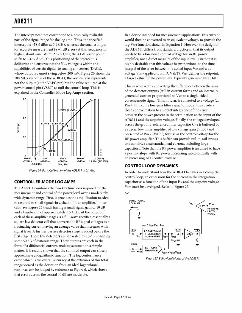
The intercept need not correspond to a physically realizable part of the signal range for the log amp. Thus, the specified intercept is −58.9 dBm at 0.1 GHz, whereas the smallest input for accurate measurement (a +1 dB error) at this frequency is higher, about −44.5 dBm. At 2.5 GHz, the +1 dB error point shifts to −47.7 dBm. This positioning of the intercept is deliberate and ensures that the VSET voltage is within the capabilities of certain digital-to-analog converters (DACs), whose outputs cannot swing below 200 mV. Figure 26 shows the 100 MHz response of the AD8311; the vertical axis represents not the output (at the VAPC pin) but the value required at the power control pin (VSET) to null the control loop. This is explained in the Controller-Mode Log Amps section.
1.5
0100μV
–67dBm1V (RMS)
13dBm (RE 50Ω)
0554
5-04
0
VIN, PIN
VSET
(V)
1mV–47dBm
10mV–27dBm
100mV–7dBm
1.0
0.5
SLOPE = 23.8mV/dB
1.211V @ –8dBm
IDEAL
448mV @ –40dBm
ACTUAL
–58.9dBm
Figure 26. Basic Calibration of the AD8311 at 0.1 GHz
CONTROLLER-MODE LOG AMPS The AD8311 combines the two key functions required for the measurement and control of the power level over a moderately wide dynamic range. First, it provides the amplification needed to respond to small signals in a chain of four amplifier/limiter cells (see Figure 25), each having a small signal gain of 10 dB and a bandwidth of approximately 3.5 GHz. At the output of each of these amplifier stages is a full-wave rectifier, essentially a square law detector cell that converts the RF signal voltages to a fluctuating current having an average value that increases with signal level. A further passive detector stage is added before the first stage. These five detectors are separated by 10 dB, spanning some 50 dB of dynamic range. Their outputs are each in the form of a differential current, making summation a simple matter. It is readily shown that the summed output can closely approximate a logarithmic function. The log conformance error, which is the overall accuracy at the extremes of this total range viewed as the deviation from an ideal logarithmic response, can be judged by reference to Figure 6, which shows that errors across the central 40 dB are moderate.
In a device intended for measurement applications, this current would then be converted to an equivalent voltage, to provide the log(VIN) function shown in Equation 1. However, the design of the AD8311 differs from standard practice in that its output needs to be a low noise control voltage for an RF power amplifier, not a direct measure of the input level. Further, it is highly desirable that this voltage be proportional to the time-integral of the error between the actual input VIN and a dc voltage VSET (applied to Pin 3, VSET). VSET defines the setpoint, a target value for the power level typically generated by a DAC.
This is achieved by converting the difference between the sum of the detector outputs (still in current form) and an internally generated current proportional to VSET to a single-sided current-mode signal. This, in turn, is converted to a voltage (at Pin 4, FLTR, the low-pass filter capacitor node) to provide a close approximation to an exact integration of the error between the power present in the termination at the input of the AD8311 and the setpoint voltage. Finally, the voltage developed across the ground-referenced filter capacitor CFLT is buffered by a special low noise amplifier of low voltage gain (×1.35) and presented at Pin 2 (VAPC) for use as the control voltage for the RF power amplifier. This buffer can provide rail-to-rail swings and can drive a substantial load current, including large capacitors. Note that the RF power amplifier is assumed to have a positive slope with RF power increasing monotonically with an increasing APC control voltage.
CONTROL LOOP DYNAMICS In order to understand how the AD8311 behaves in a complete control loop, an expression for the current in the integration capacitor as a function of the input PIN and the setpoint voltage VSET must be developed. Refer to Figure 27.
RF PA
DIRECTIONALCOUPLER POUT PCW
RF DRIVE:UP TO2.5GHz
SETPOINTINTERFACE
LOGARITHMICRF DETECTION
SUBSYSTEM
3
6
VSET
RFIN
4
CFLT
FLTR
2
VAPC
ISET = VSET/RSET
IDET IERR
IDET = ISLP PIN + IINT
VSET
VIN1.35
0554
5-04
7
Figure 27. Behavioral Model of the AD8311

AD8311
Rev. A | Page 13 of 24
Equation 6 can be restated as First, the summed detector currents are written as a function of the input power.
INTINSLPDET IPII +×= (3) ( )
sTVPVV
sV INTINSLPSETAPC
−×−= (7)
where: where: VSLP is ISLP × RSET, which has a value of 24 mV/dB. IDET is the partially filtered demodulated signal, whose steady-
state average value is extracted through the subsequent integration step.
VINT is the voltage intercept given by IINT × RSET, which has a value of 1.44 V.
T is the effective time constant for the integration and is equal to RSET × CFLT/1.35. The factor of 1.35 arises because of the voltage gain of the buffer.
ISLP is the slope, which has a value of 5.75 μA/dB. PIN is the input power in dBm (assuming 50 Ω input match). IINT is the current intercept which, as previously noted, is
dependent on the RF waveform (not the envelope). Assuming a sinusoidal input, IINT is 350 μA.
So the open-loop integration time constant can be written as
35.1FLTSETOpenLoop CRT ×= (8) The current generated by the setpoint interface is simply
SETSETSET RVI = (4) To assess the closed-loop performance, refer to the block diagram in Figure 28 and calculate the loop transfer function. In general, the buffer time constant (τBUFFER) and the log amp time constant (τLOGAMP) can be neglected, except in the case of very high PA control function gains (> than 500 dB/V) and/or very wide PA control port bandwidths. Assuming that the frequency response of the output buffer and the log amp can be neglected, the overall transfer function can be expressed as
where the RSET resistor is 4.1 kΩ. The difference between this current and IDET is applied to the loop filter capacitor CFLT. At this point note that the inclusion of a filter resistor, RFLT, can be helpful in improving the phase margin at low powers where the PA control gain (that is, ∂POUT/∂VAPC) is large, as is described later in this section. For now assume that RFLT is zero. It follows that the voltage appearing on this capacitor, VFLT, is the time-integral of the difference current.
( ) ( ) FLTDETSETFLT sCIIsV −= (5)
POUT = [ ] ( )( )
( )( )[ ] FLTPAPASLP
FLTPAPAINTSLPSET
sCsGIsCsGIII
τ+××+
×τ+××−×+
135.11)1(135.130
(9)
FLT
INTINSLPSETSET
sCIPIRV −×−
= (6) Here, GPA is the PA control function gain ∂POUT/∂VAPC given in dB/V, and the factor of −30 is due to the coupler.
The input power to the log amp, PIN, is given in dBm and therefore is simply POUT of the PA minus the coupler value, typically −30 dB, or PIN = POUT − 30.
The control output VAPC is slightly greater than this, since the gain of the output buffer is ×1.35, plus a slight offset voltage. The polarity is such that VAPC rises to its maximum value for any value of VSET greater than the equivalent value of PIN. That is, the AD8311 seeks to drive the RF power to its maximum value whenever it falls below the setpoint. The use of exact integration results in a dc error that is theoretically zero, and the logarithmic detection law would ideally result in a constant response time following a step change of either the setpoint or the power level if the power-amplifier control function were likewise linear-in-dB. This latter condition is rarely true, however, and it follows that in practice the loop response time depends on the power level. This effect can strongly influence the design of the control loop.
Equation 9 assumes that the next parasitic pole in the control loop comes from the PA. For a typical PA, a 1 MHz pole is not unusual, making this a good assumption. Therefore, except for in the case of a very wide bandwidth on the PA control port (>10 MHz), the response time and stability of the control loop is mainly determined by the characteristics of the PA. This is true for both the gain and the phase response. It is essential to understand both the magnitude and frequency response of the power amplifier control port.
1sCFLT
RFLT+IERRISET VFLT VAPC1.35
sτBUFFER1 +GPA (dB/V)1 + sτPA
POUT
–30dBCOUPLER1 + sτLOGAMP
ISLP PIN + IINT
+ _
IDET
PIN
0554
5-04
8
Figure 28. Control Loop Block Diagram

AD8311
Rev. A | Page 14 of 24
Continuing with the stability analysis, the gain of the control loop can be expressed as
kAk
IP
SET
OUT
+=
∂∂
1 (10)
where:
PA
FLTPA
ssCG
kτ+
××=
1)1(35.1
(dB/A) (11)
SLPIA = (A/dB) (12)
The effect of the zero resistor, RFLT, can be easily included by replacing (1/sCFLT) with (RFLT + 1/sCFLT). The criteria for loop stability can be derived by setting the denominator of Equation 10 equal to 0, giving
( )( ) ( )SLPPAFLTPA
FLTFLT
IGsCsCsR
××τ+
+×+=
1135.1
10 (13)
From Equation 13, the closed-loop integration time constant is given by
( )35.1××= SLPPAFLTClosedLoop IGCT (14)
The gain and phase margins of the control loop can be deduced from the Bode plots of Equation 13.
BASIC CONNECTIONS Figure 29 shows the basic connections for operating the AD8311, and Figure 30 shows a block diagram of a typical application. The AD8311 is typically used in the RF power control loop of a mobile handset.
A supply voltage of 2.7 V to 5.5 V is required for the AD8311. The supply to the VPOS pin should be decoupled with a low inductance 0.1 μF surface-mount ceramic capacitor, close to the device. The AD8311 has an internal input coupling capacitor, which negates the need for external ac-coupling. This capacitor, along with the low frequency input impedance of the device of approximately 2.14 kΩ, sets the minimum usable input frequency to around 0.016 GHz. A broadband 50 Ω input match is achieved in this example by connecting a 52.3 Ω resistor between RFIN and ground. A Smith chart plot of input impedance vs. frequency is shown in Figure 14. Other coupling methods are also possible (see the Input Coupling Options section).
VPOS
VAPC
VSET
RFIN
COMM
FLTR
AD83111
2
3 4
5
6+VS(2.7V TO 5.5V)
C10.1μF
RFIN
R152.3Ω
VAPC
VSETCFLT
0554
5-00
7
Figure 29. Basic Connections
RFIN VSETAD8311
VAPC
FLTR
CFLT
DAC
POWERAMP
RFIN
ATTENUATOR
DIRECTIONALCOUPLER
52.3Ω
RFLT
0554
5-00
8
GAINCONTROLVOLTAGE
Figure 30. Typical Application
In a power control loop, the AD8311 provides both the detector and controller functions. A sample of the power amplifier’s (PA) output power is coupled to the RF input of the AD8311, usually via a directional coupler. In dual mode applications, where there are two PAs and two directional couplers, the outputs of the directional couplers can be passively combined (both PAs will never be turned on simultaneously) before being applied to the AD8311.
A setpoint voltage is applied to VSET from the controlling source (generally this is a DAC). Any imbalance between the RF input level and the level corresponding to the setpoint voltage is corrected by the AD8311’s VAPC output that drives the gain control terminal of the PA. This restores a balance between the actual power level sensed at the input of the AD8311 and the value determined by the setpoint. This assumes that the gain control sense of the variable gain element is positive, that is, an increasing voltage from VAPC tends to increase gain.
VAPC can swing from 200 mV to within 100 mV of the supply rail and can source up to 6 mA. If the control input of the PA needs to source current, a suitable load resistor can be connected between VAPC and COMM. The output swing and current sourcing capability of VAPC is shown in Figure 11.
RANGE ON VSET AND RFIN The relationship between the RF input level and the setpoint voltage follows from the nominal transfer function of the device (see Figure 4, Figure 5, Figure 7, and Figure 8). At 0.9 GHz, for example, a voltage of 1 V on VSET indicates a demand for −18 dBm at RFIN. The corresponding power level at the output of the power amplifier is greater than this amount due to the attenuation through the directional coupler.
For setpoint voltages of less than approximately 150 mV, VAPC unconditionally remains at its minimum level of approximately 300 mV. This feature can be used to prevent any spurious emissions during power-up and power-down phases.
Above 250 mV, VSET has a linear control range up to 1.4 V, corresponding to a dynamic range of 50 dB. This results in a slope of 23.8 mV/dB, or approximately 42.0 dB/V.

AD8311
Rev. A | Page 15 of 24
TRANSIENT RESPONSE The time domain response of power amplifier control loops, using any kind of controller, is only partially determined by the choice of filter. In the case of the AD8311, the filter has a true integrator form 1/sT as shown in Equation 7, with a time constant given by Equation 8. The large signal step response is also strongly dependent on the form of the gain-control law. Nevertheless, some simple rules can be applied. When the filter capacitor CFLT is very large it dominates the time domain response, but the incremental bandwidth of this loop still varies as VAPC traverses the nonlinear gain-control function of the PA. This bandwidth is highest at the point where the slope of the tangent drawn on the PA power-control curve is greatest—that is, for power outputs near the center of the PA’s range—and is much reduced at both the minimum and the maximum power levels, where the slope of the gain control curve is lowest due to its S-shaped form.
Using smaller values of CFLT, the loop bandwidth generally increases in inverse proportion to its value. Eventually, however, a secondary effect appears due to the inherent phase lag in the power amplifier’s control path, some of which can be due to parasitic or deliberately added capacitance at the VAPC pin. This
results in the characteristic poles in the ac loop equation moving off the real axis and thus becoming complex (and somewhat resonant). This is a classic aspect of control loop design. The lowest permissible value of CFLT needs to be determined experimentally for a particular amplifier. For GSM and DCS power amplifiers, CFLT typically ranges from 150 pF to 300 pF.
In many cases, some improvement in the worst-case response time can be achieved by including a small resistor in series with CFLT; this generates an additional zero in the closed-loop transfer function, which serves to cancel a higher order pole in the overall loop. A more complex filter network can be used to minimize the settling time of the loop—for example, a combination of the main capacitor, CFLT, shunted by a second capacitor and resistor series.
MOBILE HANDSET POWER CONTROL EXAMPLE Figure 31 shows a complete power amplifier control circuit for a dual mode handset. The PF08123B (Hitachi), a dual mode (GSM, DCS) PA, is driven by a nominal power level of +3 dBm. The PA has a single gain control line; the band to be used is selected by applying either 0 V or 2 V to the PA’s VCTL input.
VAPC
VSET
2
3
VPOS RFIN
COMM
FLTR
AD8311
1
4
5
6
R152.3Ω+VS
2.7V
8-BITRAMP DAC0V–2.55V
1R2, R3 OPTIONAL, SEE TEXT
TO
1000pFBAND
SELECT0V/+2V
3.5V
1000pF
4.7 Fμ 4.7 Fμ
1000pF
POUT DCS32dBm MAX
POUT GSM35dBm MAX
3
4
1
5
8
7LDC15D190A0007A
6 2
49.9Ω
ATTN20dB
PF08123B
VCTL
VAPC
(OPTIONAL,SEE TEXT)
500Ω
PIN GSM3dBm
PIN DCS3dBm
0.1μF
R311kΩ
1.5kΩ
150pF
R21600Ω
TO ANTENNA
0554
5-04
9
Figure 31. Dual Mode (GSM/DCS) PA Control Example

AD8311
Rev. A | Page 16 of 24
Some of the output power from the PA is coupled off using a dual-band directional coupler (Murata part number LDC15D190A0007A). This has a coupling factor of approximately +19 dB for the GSM band and +14 dB for DCS and an insertion loss of 0.38 dB and 0.45 dB, respectively. Because the PF08107B transmits a maximum power level of +35 dBm for GSM and +32 dBm for DCS, additional attenuation of 20 dB is required before the coupled signal is applied to the AD8311. This results in peak input levels to the AD8311 of −4 dBm (GSM) and −2 dBm (DCS). While the AD8311 gives a linear response for input levels up to +2 dBm, for highly temperature-stable performance at maximum PA output power the maximum input level should be limited to approximately −2 dBm (see Figure 5 and Figure 7). This does, however, reduce the sensitivity of the circuit at the low end.
The operational setpoint voltage, in the range 250 mV to 1.4 V, is applied to the VSET pin of the AD8311. This typically is supplied by a DAC. The AD8311’s VAPC output drives the level control pin of the power amplifier directly. VAPC reaches a maximum value of approximately 2.5 V on a 2.7 V supply while delivering the 3 mA required by the level control input of the PA. This is more than sufficient to exercise the gain control range of the PA.
During initialization and completion of the transmit sequence, VAPC should be held at its minimum level of 300 mV by keeping VSET below 150 mV.
In this example, VSET is supplied by an 8-bit DAC that has an output range from 0 V to 2.55 V or 10 mV per bit. This sets the control resolution of VSET to 0.4 dB/bit (0.04 dB/mV times 10 mV). If finer resolution is required, the DAC’s output voltage can be scaled using two resistors as shown. This converts the DAC’s maximum voltage of 2.55 V down to 1.6 V and increases the control resolution to 0.25 dB/bit.
A filter capacitor (CFLT) must be used to stabilize the loop. The choice of CFLT depends to a large degree on the gain control dynamics of the power amplifier, something that is frequently poorly characterized, so some trial and error might be necessary.
In this example, a 150 pF capacitor is used and a 1.5 kΩ series resistor is included. This adds a zero to the control loop and increases the phase margin, which helps to make the step response of the circuit more stable when the PA output power is low and the slope of the PA’s power control function is the steepest.
A smaller filter capacitor can be used by inserting a series resistor between VAPC and the control input of the PA. A series resistor works with the input impedance of the PA to create a resistor divider, which reduces the loop gain. The size of the resistor divider ratio depends on the available output swing of VAPC and the required control voltage on the PA.
This technique can also be used to limit the control voltage in situations where the PA cannot deliver the power level being demanded by VAPC. Overdrive of the control input of some PAs causes increased distortion. It should be noted, however, that if the control loop opens (that is, VAPC goes to its maximum value in an effort to balance the loop), the quiescent current of the AD8311 increases somewhat, particularly at supply voltages greater than 3 V.
Figure 32 shows the relationship between VSET and output power (POUT) at 0.9 GHz. The overall gain control function is linear in dB for a dynamic range of over 40 dB. Note that for VSET voltages below 300 mV, the output power drops off steeply as VAPC drops toward its minimum level of 300 mV.
40
–200 1.6
0554
5-04
1
SETPOINT VOLTAGE (V)
OU
TPU
T PO
WER
(dB
m)
30
20
10
0
–10
0.2 0.4 0.6 0.8 1.0 1.2 1.4
3
–3
2
1
0
–1
–2
ERR
OR
(dB
)
–40°C+25°C
+85°C
–40°C
+25°C
+85°C
Figure 32. POUT vs. VSET at 0.9 GHz for Dual Mode Handset
Power Amplifier Application; −40°C, +25°C, and +85°C
POWER-ON AND POWER-OFF The AD8311 can be completely disabled by pulling the supply voltage to ground. The voltage on VSET should be kept below 150 mV during power-on and power-off to prevent any unwanted transients on VAPC.
INPUT COUPLING OPTIONS The internal 5 pF coupling capacitor of the AD8311 and the low frequency input impedance of 2.14 kΩ give a high-pass input corner frequency of approximately 16 MHz. This sets the minimum operating frequency. Figure 33, Figure 34, and Figure 35 shows three options for input coupling. A broadband resistive match can be implemented by connecting a shunt resistor to ground at RFIN (Figure 33). This 52.3 Ω resistor (other values can also be used to select different overall input impedances) combines with the input impedance of the AD8311 to give a broadband input impedance of 50 Ω. While the input resistance and capacitance (CIN and RIN) of the AD8311 vary from device to device by approximately ±20%, as well as in the same device over a range of frequencies (Figure 14), the dominance of the external shunt resistor means that the variation in the overall input impedance is close to the

AD8311
Rev. A | Page 17 of 24
tolerance of the external resistor. This method of matching is most useful in wideband applications or in multiband systems where there is more than one operating frequency.
A reactive match can also be implemented as shown in Figure 34. This is not recommended at low frequencies because device tolerances dramatically vary the quality of the match due to the large input resistance. For low frequencies, Figure 33 or Figure 35 is recommended.
In Figure 34, the matching components are drawn as generic reactances. Depending on the frequency, the input impedance, and the availability of standard value components either a capacitor or an inductor is used. As in the previous case, the input impedance at a particular frequency is plotted on a Smith Chart and matching components are chosen (shunt or series L, shunt or series C) to move the impedance to the center of the chart.
RFIN
AD8311
RINCIN
CC
RSHUNT52.3Ω
0554
5-00
9
Figure 33. Broadband Resistive Input Coupling Option
RFIN
AD8311
x2 RINCIN
CCx1
0554
5-01
0
Figure 34. Narrow Band Reactive Input Coupling Option
RFIN
AD8311
RINCIN
CC
RATTN
ANTENNA
STRIPLINE
PA
0554
5-01
1
Figure 35. Series Attention Input Coupling Option
Figure 35 shows a third method for coupling the input signal into the AD8311. A series resistor connected to the RF source combines with the input impedance of the AD8311 to resistively divide the input signal being applied to the input. This has the advantage of very little power being tapped off in RF power transmission applications.
TEMPERATURE DRIFT Figure 36 shows the log slope and error over temperature for a 0.9 GHz input signal. Error due to drift over temperature consistently remains within ±1 dB and only begins to exceed this limit when the ambient temperature goes above +65 °C and below −20 °C. For all frequencies using a reduced temperature range, higher measurement accuracy is achievable.
10
–600.2 1.6
0554
5-04
2
VSET (V)PI
N (d
Bm
)
0
–10
–20
–30
–40
–50
0.4 0.6 0.8 1.0 1.2 1.4
4
–3
2
1
0
–1
–2
ERR
OR
(dB
)
3
–40°C–20°C0°C+25°C+45°C+65°C+85°C
Figure 36. Typical Drift at 900 GHz for Various Temperatures
DEVICE CALIBRATION AND ERROR CALCULATION The measured transfer function of the AD8311 at 0.9 GHz is shown in Figure 37. The figure shows plots of both input power and calculated error vs. setpoint voltage.
The vertical axis represents the input power required at the RFIN pin to null the control loop when a VSET voltage is applied. As the setpoint voltage varies from about 0.2 V to 1.5 V, the corresponding input power varies from −60 dBm to +10 dBm.
10
–600 1.6
0554
5-04
3
VSET (V)
RFI
N (d
Bm
)
0
–10
–20
–30
–40
–50
4
–3
2
1
0
–1
–2
ERR
OR
(dB
)
3
0.2 0.4 0.6 0.8 1.0 1.2 1.4
PIN2
PIN1
VSET1INTERCEPT
VSET2
PINIDEAL = (VSET1/ SLOPE) + INTERCEPTERROR (dB) = (PINIDEAL – PIN)SLOPE = (VSET2 – VSET1)/(PIN1 – PIN2)INTERCEPT = PIN1 – (VSET1 / SLOPE)
+85°C
–40°C
+25°C
–40°C
+25°C+85°C
Figure 37. Transfer Function of AD8311 at 0.9 GHz
Because slope and intercept vary from device to device, board-level calibration must be performed to achieve high accuracy.

AD8311
Rev. A | Page 18 of 24
In a control loop, calibration is performed by applying two levels to the AD8311’s setpoint voltage and measuring the corresponding power. The calibration points are generally chosen to be within the linear-in-dB operating range of the device (see Figure 37). Calculation of slope and intercept is done using the equations
)/()( 1IN2IN1SET2SET PPVVSLOPE −−= (15)
)/( SLOPEVPINTERCEPT 1SET1IN −= (16)
Once slope and intercept have been calculated, an equation can be written which allows calculation of an (unknown) power based on the setpoint voltage.
INTERCEPTSLOPEVP SETIN += )/( (17)
Using Equation 17 as a reference for the ideal input power, the log conformance error of the measured data can be calculated:
)()( DIN,MEASUREIN,IDEAL PPdBERROR −= (18)
Figure 37 includes a plot of the error at 25°C, the temperature at which the AD8311 is calibrated. Note that the error is not zero. This is because the AD8311 does not perfectly follow the ideal VSET vs. PIN equation, even within its operating region. The error at the calibration points (0.45 V and 1.15 V in this case) is, however, equal to zero by definition.
Figure 37 also includes error plots for the output voltage at −40°C and +85 °C. These error plots are calculated using the slope and intercept at +25°C. This is consistent with calibration in a mass-production environment where calibration at temperature is not practical.
SELECTING CALIBRATION POINTS TO IMPROVE ACCURACY OVER A REDUCED RANGE In some applications very high accuracy is required at just one power level or over a reduced input range. For example, in a wireless transmitter, the accuracy of the high power amplifier (HPA) is most critical at or close to full power.
Figure 38 shows the same measured data as Figure 37. Notice that accuracy is very high from −15 dBm to 0 dBm. Below −15 dBm the error increases to about −2 dB. This is because the calibration points have been changed to approximately 0.975 V and 1.3 V.
10
–600 1.6
0554
5-04
4
VSET (V)
RFI
N (d
Bm
)
0
–10
–20
–30
–40
–50
4
–3
2
1
0
–1
–2
ERR
OR
(dB
)
3
0.2 0.4 0.6 0.8 1.0 1.2 1.4
PIN1
PIN2
VSET2
VSET1
–40°C+25°C+85°C
–40°C
+25°C
+85°C
Figure 38. Output Voltage and Error vs. PIN with 2-Point Calibration at
Approximately 0.975 V and 1.3 V
Calibration points should be chosen to suit the application at hand. In general, though, the calibration points should never be chosen in the nonlinear portion of the log amp’s transfer function (above 1.4 V or below 0.35 V in this case).
Figure 39 shows how calibration points can be adjusted to increase dynamic range, but at the expense of linearity. In this case the calibration points for slope and intercept are set at 0.37 V and 1.37 V. These points are at the end of the device’s linear range. Once again at 25°C we see an error of 0 dB at the calibration points. Note also that the range over which the AD8311 maintains an error of less than ±0.5 dB is extended to more than 45 dB at 25°C and more than 40 dB over temperature. The disadvantage of this approach is that linearity suffers, especially in the middle of the range.
10
–600 1.6
0554
5-04
5
VSET (V)
RFI
N (d
Bm
)
0
–10
–20
–30
–40
–50
4
–3
2
1
0
–1
–2
ERR
OR
(dB
)
3
0.2 0.4 0.6 0.8 1.0 1.2 1.4
PIN2
VSET2
VSET1
PIN1
–40°C+25°C+85°C
–40°C
+25°C
+85°C
Figure 39. Dynamic Range Extension by Choosing Calibration Points that are
Close to the End of the AD8311’s Linear Range

AD8311
Rev. A | Page 19 of 24
10
–600 1.6
0554
5-04
6
VSET (V)
RFI
N (d
Bm
)
0
–10
–20
–30
–40
–50
4
–3
2
1
0
–1
–2
ERR
OR
(dB
)
3
0.2 0.4 0.6 0.8 1.0 1.2 1.4
–40°C+25°C+85°C
–40°C
+25°C
DOES NOT TAKE INTO ACCOUNT TRANSFERFUNCTIONS’ NONLINEARITIES AT +25°C
+85°C
Another way of presenting the error function of a log amp detector is shown in Figure 40. In this case, the dB error at hot and cold temperatures is calculated with respect to the transfer function at ambient. This is a key difference in comparison to the previous plots. Up to now, all errors have been calculated with respect to the ideal transfer function at ambient.
When we use this alternative technique, the error at ambient becomes by definition equal to 0 (see Figure 40).
This would be valid if the device transfer function perfectly followed the ideal PIN = VSET / SLOPE + INTERCEPT equation. However since a log amp in practice never perfectly follows this equation (especially outside of its linear operating range), this plot tends to artificially improve linearity and extend the dynamic range. This plot is a useful tool for estimating temperature drift at a particular power level with respect to the (nonideal) response at ambient. However, achieving this level of accuracy in an end application requires calibration at multiple points in the device’s operating range.
Figure 40. Error vs. Temperature with respect to Output Voltage at 25 °C
DEVICE HANDLING The wafer-level chip scale package consists of solder bumps connected to the active side of the die. The part is lead-free with 95.5% tin, 4.0% silver, and 0.5% copper solder bump composition. The WLCSP package can be mounted on printed circuit boards using standard surface-mount assembly techniques; however, caution should be taken to avoid damaging the die. See the AN-617 application note for additional information. WLCSP devices are bumped die, and exposed die can be sensitive to light condition, which can influence specified limits.

AD8311
Rev. A | Page 20 of 24
EVALUATION BOARD Figure 41 shows the schematic of the AD8311 WLCSP evaluation board. The layout and silkscreen of the component and circuit sides are shown in Figure 42 to Figure 45. The board is powered by a single supply in the range 2.7 V to 5.5 V. The power supply is decoupled by a 0.1 μF capacitor. A 100 pF capacitor provides additional supply decoupling, but is not necessary for basic operation.
Table 5 details the various configuration options of the evaluation board.
For operation in controller mode, both jumpers J1 and J2 should be removed. The setpoint voltage is applied to VSET, RFIN is connected to the RF source (PA output or directional coupler), and VAPC is connected to the gain control pin of the PA. When used in controller mode, a capacitor must be installed in C4 for loop stability (R2 must also be installed, 0 Ω
by default). For GSM/DCS handset power amplifiers, this capacitor should typically range from 150 pF to 300 pF.
A quasi-measurement mode (where the AD8311 delivers an output voltage that is proportional to the log of the input signal) can be implemented, to establish the relationship between VSET and RFIN, by installing the two jumpers J1 and J2. This mimics an AGC loop. To establish the transfer function of the log amp, the RF input should be swept while the voltage on VSET is measured, that is, the SMA connector labeled VSET now acts as an output. This is the simplest method to validate operation of the evaluation board. When operated in this mode, a large capacitor (0.01 μF or greater) must be installed in C4 (filter capacitor) to ensure loop stability. The op amp must be powered with a nominal voltage of 2.7 V to 5.5 V with the VS supply. Alternately, J3 can be installed to power the op amp with the AD8311’s VPOS power supply.
1
2
3
VAPC
VPOSAD8311
6
5
4VSET
COMM
RFIN
FTLR
C2100pF
C10.1μF
52.3Ω
VPOS RFIN
VAPC0Ω
R3
R4(OPEN)
C3(OPEN)
J2
R1
(OPEN)C4
0ΩR2
J1
R10(OPEN)
R510kΩ
R817.8kΩ
(OPEN)R9
TO EDGECONNECTOR
R610kΩ
R716.2kΩ
VPOS
0.1μFC5
0.1μFC6
VSET
(OPEN)C7
J3 VS
0554
5-01
2
TO EDGECONNECTOR
Figure 41. Evaluation Board Schematic

AD8311
Rev. A | Page 21 of 24
0554
5-01
3
Figure 42. Layout of Component Side (WLCSP)
0554
5-01
3
Figure 43. Layout of Circuit Side (WLCSP)
0554
5-01
5
Figure 44. Silkscreen of Component Side (WLCSP)
0554
5-01
6
Figure 45. Silkscreen of Circuit Side (WLCSP)
Table 5. Evaluation Board Configuration Options Component Function Default Condition VPOS, GND Supply and Ground Vector Pins. Not Applicable R1 Input Interface. The 52.3 Ω resistor in Position R1 combines with the AD8311’s internal input
impedance to give a broadband input impedance of around 50 Ω. Note that the AD8311’s RF input is internally ac-coupled.
R1 = 52.3 Ω (Size 0402)
R3, R4, C3 Output Interface. R4 and C3 can be used to check the response of VAPC to capacitive and resistive loading. R3/R4 can be used to reduce the slope of VAPC.
R3 = 0 Ω (Size 0402) R4 = C3 = open (Size 0402)
C1, C2 Power Supply Decoupling. The nominal supply decoupling consists of a 0.1 μF capacitor at C1. C2 can be used for additional supply decoupling.
C1 = 0.1 μF (Size 0402) C2 = 100 pF (Size 0402)
C4, R2 Filter Capacitor. The response time of VAPC can be modified by placing a capacitor between FLTR (Pin 4) and ground. The control loop phase margin can be increased by adding a series resistor.
C4 = open (Size 0402) R2 = 0 Ω (Size 0402)
J1, J2, J3 Measurement Mode. A quasi-measurement mode can be implemented by installing J1 and J2 (connecting an inverted VAPC to VSET) to yield the nominal relationship between RFIN and VSET. In this mode, a large capacitor (0.01 μF or greater) must be installed in C4. J3 can be installed to power the op-amp with the VPOS power supply. Alternately, the op-amp can be powered with the VS supply pin.
J1, J2 = installed J3 = installed
R9, R10 Alternate Interface. R5 and R6 allow for VOUT and VSET to be accessible from the edge connector, which is only used for characterization.
R9 = R10 = open (Size 0402)

AD8311
Rev. A | Page 22 of 24
OUTLINE DIMENSIONS
0.50 BSC
1.00BSC1.50
1.451.40
1.000.950.90
SEATINGPLANE
0.6750.5950.515
0.075COPLANARITY
0.3800.3550.330
0.3450.2950.245
0.2700.2400.210
A1 BALLCORNER
0.50BSC
A
12
B
C
TOP VIEW(BALL SIDE DOWN)
BOTTOM VIEW(BALL SIDE UP)
0816
07-B
Figure 46. 6-Ball Wafer Level Chip Scale Package [WLCSP]
(CB-6-2) Dimensions shown in millimeters
ORDERING GUIDE
Model1 Temperature Range Package Description
Package Option Branding
Ordering Quantity
AD8311ACBZ-P7 –40°C to +85°C 6-Ball Wafer Level Chip Scale Package [WLCSP], 7” Pocket Tape and Reel
CB-6-2 Q04 3000
AD8311ACBZ-P2 –40°C to +85°C 6-Ball Wafer Level Chip Scale Package [WLCSP], 7” Pocket Tape and Reel
CB-6-2 Q04 250
AD8311-EVAL Evaluation Board
1 Z = RoHS Compliant Part.

AD8311
Rev. A | Page 23 of 24
NOTES

AD8311
Rev. A | Page 24 of 24
NOTES
©2005–2011 Analog Devices, Inc. All rights reserved. Trademarks and registered trademarks are the property of their respective owners. D05545-0-1/11(A)