Embed Size (px)
Citation preview
1
PROCESSOR:PROCESSOR:DATAPATH & CONTROL DATAPATH & CONTROL -- 22
Dr. Bill YiSanta Clara University
(Based on text: David A. Patterson & John L. Hennessy, Computer Organization and Design: The Hardware/Software Interface, 3rd Ed., Morgan Kaufmann, 2007)
(Also based on presentation: Dr. Nam Ling, COEN210 Lecture Notes)

2
COURSE CONTENTSCOURSE CONTENTSIntroductionInstructionsComputer ArithmeticPerformanceProcessor: Processor: DatapathDatapathProcessor: ControlProcessor: ControlPipelining TechniquesMemoryInput/Output Devices

3
PROCESSOR: PROCESSOR: DATAPATH & CONTROLDATAPATH & CONTROL
Multi-Cycle Datapath & ControlControl: Finite State Machine (FSM)Control: Microprogramming
4
Break up an instruction into steps, each step takes a cycle:balance the amount of work to be donerestrict each cycle to use only one major functional unitDifferent instructions take different number of cycles to complete
At the end of a cycle:store values for use in later cycles (easiest thing to do)introduce additional “internal” registers for such temporalstorage
Reusing functional units (reduces hardware cost):Use ALU to compute address/result and to increment PCUse memory for both instructions and data
Multicycle ApproachMulticycle Approach

5
Additional “internal registers”:Instruction register (IR) -- to hold current instruction Memory data register (MDR) -- to hold data read from memoryA register (A) & B register (B) -- to hold register operand values from register filesALUOut register (ALUOut) -- to hold output of ALU, also serves as memory address register (MAR)
All registers except IR hold data only between a pair of adjacent cycles and thus do not need writecontrol signals; IR holds instructions till end of instruction, hence needs a write control signal
MultiMulti--Cycle Datapath:Cycle Datapath:Additional RegistersAdditional Registers
Shiftleft 2
PC
MemoryData
Writedata
Mux
0
1Registers
Writeregister
Writedata
Readdata 1
Readdata 2
Readregister 1
Readregister 2
Mux
0
1
Mux
0
1
4
Instruction[15– 0]
Signextend
3216
Instruction[25– 21]
Instruction[20– 16]
Instruction[15– 0]
Instructionregister
1 Mux
0
32
Mux
ALUresult
ALUZero
Memorydata
register
Instruction[15– 11]
A
B
ALUOut
0
1
Address
Inst /
Note: we ignore jump inst here
6
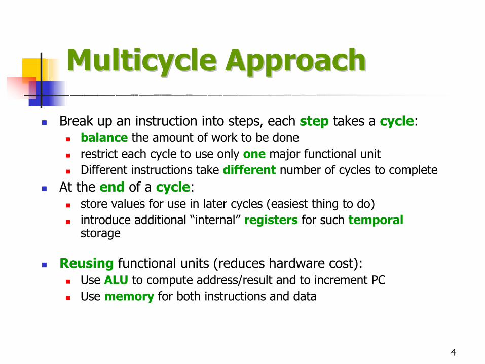
Additional multiplexors:Mux for first ALU input -- to select A or PC (since we use ALU for both address/result computation & PC increment) Bigger mux for second ALU input -- due to two additional inputs: 4 (for normal PC increment) and the sign-extended & shifted offset field (in branch address computation)Mux for memory address input -- to select instruction address or data address
Multicycle Datapath:Multicycle Datapath:Additional Additional MultiplexorsMultiplexors
Shiftleft 2
PC
MemoryData
Writedata
Mux
0
1Registers
Writeregister
Writedata
Readdata 1
Readdata 2
Readregister 1
Readregister 2
Mux
0
1
Mux
0
1
4
Instruction[15– 0]
Signextend
3216
Instruction[25– 21]
Instruction[20– 16]
Instruction[15– 0]
Instructionregister
1 Mux
0
32
Mux
ALUresult
ALUZero
Memorydata
register
Instruction[15– 11]
A
B
ALUOut
0
1
Address
Inst /
Note: we ignore jump inst here
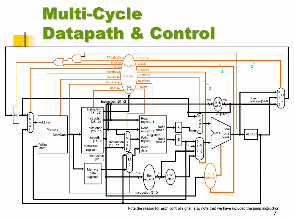
7
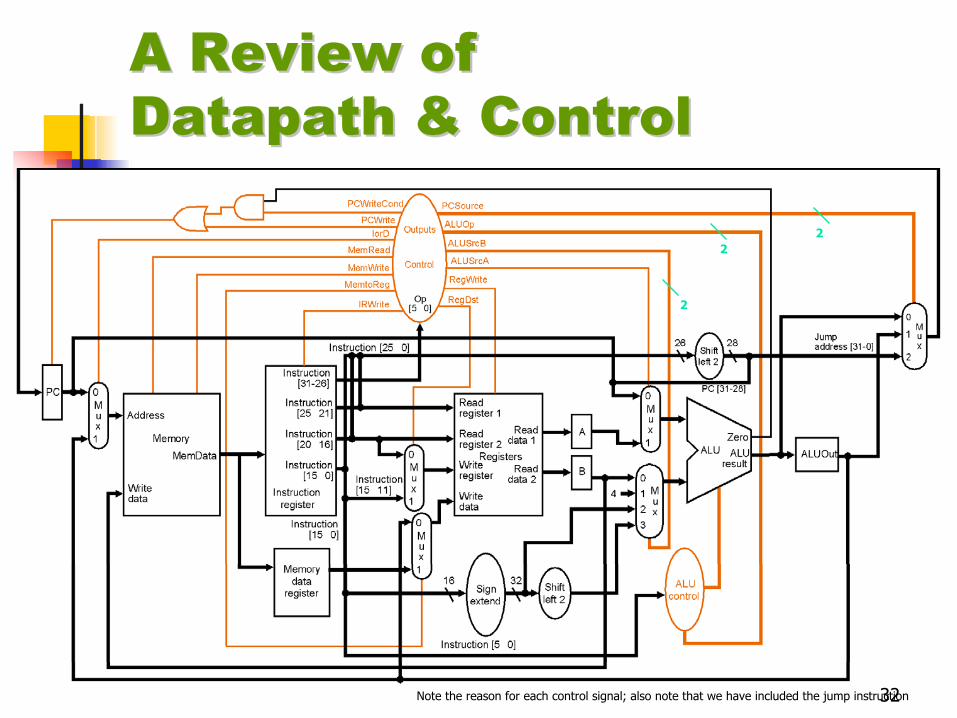
MultiMulti--CycleCycleDatapathDatapath & Control& Control
Note the reason for each control signal; also note that we have included the jump instruction
2
2
2
8
Note:three possible sources for value to be written into PC (controlled by PCSource): (1) regular increment of PC, (2) conditional branch target from ALUOut, (3) unconditional jump (lower 26 bits of instruction in IR shifted left by 2 and concatenated with upper 4 bits of the incremented PC)two PC write control signals: (1) PCWrite (for unconditional jump), & (2) PCWriteCond (for “zero” signal to cause a PC write if asserted during beqinst.)since memory is used for both inst. & data, need IorD to select appropriate addressesIRWrite needed for IR so that instruction is written to IR (IRWrite = 1) during the first cycle of the instruction and to ensure that IR not be overwritten by another instruction during the later cycles of the current instruction execution (by keeping IRWrite = 0)other control signals
Control Signals forControl Signals forMultiMulti--Cycle DatapathCycle Datapath

9
1. Instruction Fetch (All instructions)2. Instruction Decode (All instructions), Register Fetch & Branch Address
Computation (in advance, just in case) 3. ALU (R-type) execution, Memory Address Computation, or Branch
Completion (Instruction dependent)4. Memory Access or R-type Instruction Completion (Instruction dependent)5. Memory Read Completion (only for lw)
At end of every clock cycle, needed data must be stored into register(s) or memory location(s).
Each step (can be several parallel operations) is 1 clock cycle --> Instructions take 3 to 5 cycles!
Breaking the InstructionBreaking the Instructioninto 3 into 3 -- 5 Execution Steps5 Execution Steps
Data ready operation Clock in result
ClockEvents during a cycle, e.g.:

10
Use PC to get instruction (from memory) and put it in the Instruction RegisterIncrement of the PC by 4 and put the result back in the PCCan be described succinctly using RTL "Register-Transfer Language"
IR <= Memory[PC];PC <= PC + 4;
Which control signals need to be asserted?IorD = 0, MemRead = 1, IRWrite = 1ALUSrcA = 0, ALUSrcB = 01, ALUOp = 00, PCWrite = 1, PCSource = 00
Why can instruction read & PC update be in the same step? Look at state element timing
What is the advantage of updating the PC now?
Step 1: Instruction FetchStep 1: Instruction Fetch
11
In this step, we decode the instruction in IR (the opcode enters control unit in order to generate control signals). In parallel, we canRead registers rs and rt, just in case we need themCompute the branch address, just in case the instruction is a branch beqRTL:
A <= Reg[IR[25:21]];B <= Reg[IR[20:16]];ALUOut <= PC + (sign-extend(IR[15:0]) << 2);
Control signals: ALUSrcA = 0, ALUSrcB = 11, ALUOp = 00 (add)Note: no explicit control signals needed to write A, B, & ALUOut. They are written by clock transitions automatically at end of step
Step 2: Instruction Decode, Reg. Step 2: Instruction Decode, Reg. Fetch, & Branch Fetch, & Branch AddrAddr. Comp.. Comp.

12
One of four functions, based on instruction type:
Memory address computation (for lw, sw):ALUOut <= A + sign-extend(IR[15:0]);
Control signals: ALUSrcA = 1, ALUSrcB = 10, ALUOp = 00ALU (R-type):
ALUOut <= A op B;Control signals: ALUSrcA = 1, ALUSrcB = 00, ALUOp = 10Conditional branch:
if (A==B) PC <= ALUOut;Control signals: ALUSrcA = 1, ALUSrcB = 00, ALUOp = 01 (Sub), PCSource = 01,PCWriteCond = 1 (to enable zero to write PC if 1)What is the content of ALUOut during this step? Immediately after this step?Jump:
PC <= PC[31:28] || (IR[25:0]<<2);Control signals: PCSource = 10, PCWrite = 1
Note: Conditional branch & jump instructions completed at this step!
Step 3: InstructionStep 3: InstructionDependent OperationDependent Operation

13
For lw or sw instructions (access memory):
MDR <= Memory[ALUOut];or
Memory[ALUOut] <= B;
Control signals (for lw): IorD = 1 (to select ALUOut as address), MemRead = 1, note that no write signal needed for writing to MDR, it is written by clock transition automatically at end of stepControl signals (for sw): IorD = 1 (to select ALUOut as address), MemWrite = 1
For ALU (R-type) instructions (write result to register):
Reg[IR[15:11]] <= ALUOut;
Control signals: RegDst = 1 (to select register address), MemtoReg = 0, RegWrite = 1
The write actually takes place at the end of the cycle on the clock edge!Note: sw and ALU (R-type) instructions completed at this step!
Step 4: Memory Access or ALUStep 4: Memory Access or ALU(R(R--type) Instruction Completiontype) Instruction Completion
14
For lw instruction only (write data from MDR to register):
Reg[IR[20:16]]<= MDR;
Control signals: RegDst = 0 (to select register address), MemtoReg = 1, RegWrite = 1
Note: lw instruction completed at this step!
Step 5: Memory Read Step 5: Memory Read CompletionCompletion

15
Summary of Execution StepsSummary of Execution Steps
Step nameAction for R-type
instructionsAction for memory-reference
instructionsAction for branches
Action for jumps
Instruction fetch IR <= Memory[PC]PC <= PC + 4
Instruction A <= Reg [IR[25:21]]decode/register fetch B <= Reg [IR[20:16]]/branch addr comp ALUOut <= PC + (sign-extend (IR[15:0]) << 2)Execution, address ALUOut <= A op B ALUOut <= A + sign-extend if (A ==B) then PC <= PC [31:28]computation, branch/ (IR[15:0]) PC <= ALUOut II (IR[25:0]<<2)jump completionMemory access or R-type Reg [IR[15:11]] <= Load: MDR <= Memory[ALUOut]completion ALUOut or
Store: Memory [ALUOut] <= B
Memory read completion Load: Reg[IR[20:16]] <= MDR
Some instructions take shorter number of cycles, therefore next instructions can start earlier.Hence, compare to single-cycle implementation where all instructions take same amount of time, multi-cycle implementation is faster!Multi-cycle implementation also reduces hardware cost (reduces adders & memory, increases number of registers & muxes).
16
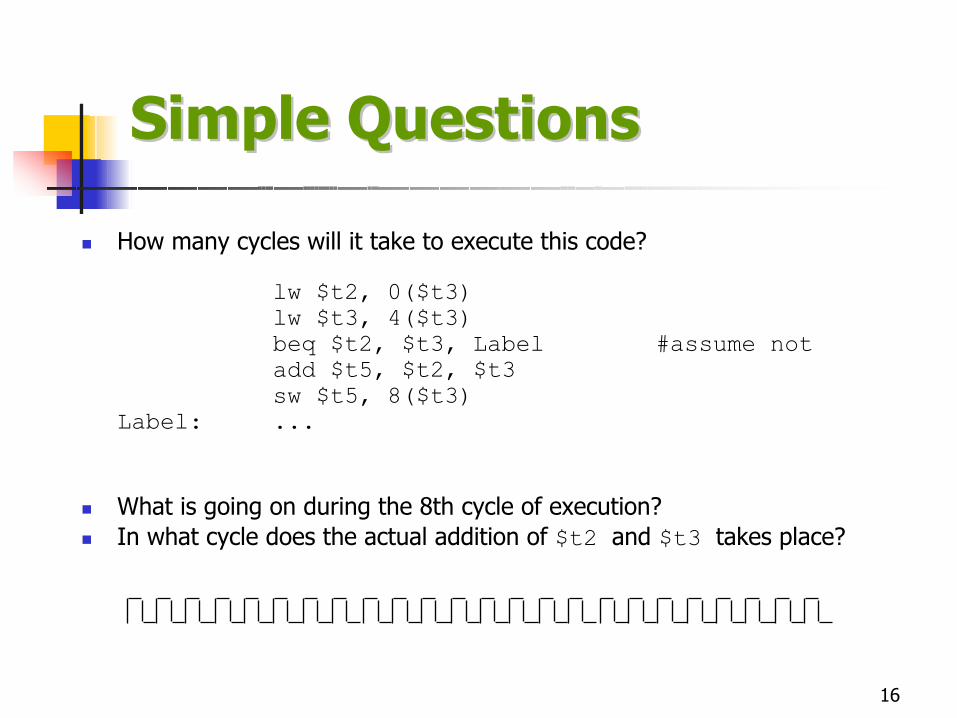
How many cycles will it take to execute this code?
lw $t2, 0($t3)lw $t3, 4($t3)beq $t2, $t3, Label #assume notadd $t5, $t2, $t3sw $t5, 8($t3)
Label: ...
What is going on during the 8th cycle of execution?In what cycle does the actual addition of $t2 and $t3 takes place?
Simple QuestionsSimple Questions

17
Multi-cycle vs single-cycle datapath:for single-cycle, truth-tables to specify setting of control signals based on instructionfor multi-cycle, control is more complex due to instruction is executed in steps; control must specify both the control signals in any step & the next step in the sequence
Value of control signals dependent upon:what instruction is being executedwhich step is being performed
Two different control techniques:Finite state machine (FSM)Microprogramming
Implementation can be derived from specification
Defining the Control for Defining the Control for MultiMulti--Cycle DatapathCycle Datapath

18
Consists of set of states & directions on how to change statesEach state specifies a set of control signal outputs that are asserted when machine is at that stateEach state in FSM takes 1 clock cycleFirst two states (state 0 & state 1) common for all instructionsAfter state 1, signals asserted depend on instruction (this process is called instruction decoding)After last step (state) of an instruction, FSM returns to state 0 to begin fetching next instruction
Finite State MachineFinite State Machine(FSM) Control(FSM) Control

19
The Complete FSM ControlThe Complete FSM Control
PCWritePCSource = 10
ALUSrcA = 1ALUSrcB = 00ALUOp = 01PCWriteCond
PCSource = 01
ALUSrcA =1ALUSrcB = 00ALUOp= 10
RegDst = 1RegWrite
MemtoReg = 0MemWriteIorD = 1
MemReadIorD = 1
ALUSrcA = 1ALUSrcB = 10ALUOp = 00
RegDst =0RegWrite
MemtoReg =1
ALUSrcA = 0ALUSrcB = 11ALUOp = 00
MemReadALUSrcA = 0
IorD = 0IRWrite
ALUSrcB = 01ALUOp = 00
PCWritePCSource = 00
Instruction fetch Instruction decode/register fetch
Jumpcompletion
BranchcompletionExecution
Memory addresscomputation
Memoryaccess
Memoryaccess R-type completion
Write-back step
(Op = 'LW') or (Op = 'SW') (Op = R-type)
(Op = 'BEQ')
(Op
='J'
)
( Op = 'SW')
(Op
='LW
')
4
01
9862
753
Start
Graphical specification:

20
CPI in MultiCPI in Multi--Cycle CPUCycle CPU
load store R-type branch(cond.)
jumps
gcc instructionmix
22% 11% 49% 16% 2%
#cycles 5 4 4 3 3
CPI = 0.22 x 5 + 0.11 x 4 + 0.49 x 4 + 0.16 x 3 + 0.02 x 3
= 1.1 + 0.44 + 1.96 + 0.48 + 0.06 = 4.04
Better than worst case CPI (if all instructions took same number of cycles = 5)
Example:
21
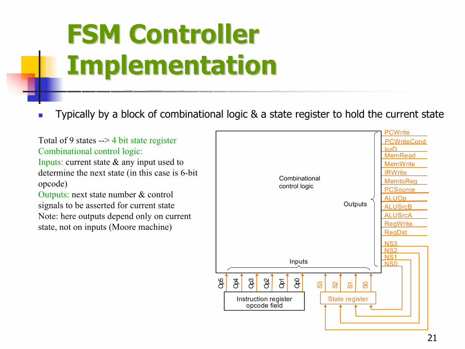
Typically by a block of combinational logic & a state register to hold the current state
FSM Controller FSM Controller ImplementationImplementation
PCWritePCWriteCondIorD
MemtoRegPCSourceALUOpALUSrcBALUSrcARegWriteRegDst
NS3NS2NS1NS0
Op5
Op4
Op3
Op2
Op1
Op0
S3 S2 S1 S0
State register
IRWrite
MemReadMemWrite
Instruction registeropcode field
Outputs
Combinational control logic
Inputs
Total of 9 states --> 4 bit state registerCombinational control logic:Inputs: current state & any input used to determine the next state (in this case is 6-bit opcode)Outputs: next state number & control signals to be asserted for current stateNote: here outputs depend only on current state, not on inputs (Moore machine)
22
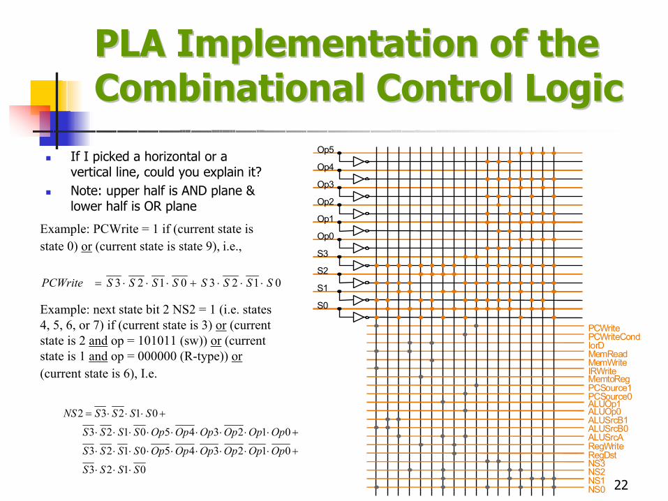
PLA Implementation of the PLA Implementation of the Combinational Control LogicCombinational Control Logic
If I picked a horizontal or a vertical line, could you explain it?Note: upper half is AND plane & lower half is OR plane
Op5
Op4
Op3
Op2
Op1
Op0
S3
S2
S1
S0
IorD
IRWrite
MemReadMemWrite
PCWritePCWriteCond
MemtoRegPCSource1
ALUOp1
ALUSrcB0ALUSrcARegWriteRegDstNS3NS2NS1NS0
ALUSrcB1ALUOp0PCSource0
01230123 SSSSSSSSPCWrite ⋅⋅⋅+⋅⋅⋅=
Example: PCWrite = 1 if (current state is state 0) or (current state is state 9), i.e.,
Example: next state bit 2 NS2 = 1 (i.e. states 4, 5, 6, or 7) if (current state is 3) or (current state is 2 and op = 101011 (sw)) or (current state is 1 and op = 000000 (R-type)) or(current state is 6), I.e.
0123
0123450123
0123450123
01232
SSSS
OpOpOpOpOpOpSSSS
OpOpOpOpOpOpSSSS
SSSSNS
⋅⋅⋅
+⋅⋅⋅⋅⋅⋅⋅⋅⋅
+⋅⋅⋅⋅⋅⋅⋅⋅⋅
+⋅⋅⋅=

23
Combinational control logic can be express in a truth table: inputs are current state values (S3 - S0) & Opcodes (Op5 - Op0); outputs are control signals & next state values (NS3 - NS0)A ROM can be used to implement a truth table
if the address (inputs) is m-bits, we can address 2m entries in the ROMoutputs are the bits of data that the address points to
ROM Implementation of ROM Implementation of Combinational Control LogicCombinational Control Logic
0 0 0 0 0 1 10 0 1 1 1 0 00 1 0 1 1 0 00 1 1 1 0 0 0 1 0 0 0 0 0 0 1 0 1 0 0 0 11 1 0 0 1 1 01 1 1 0 1 1 1
address dataExample:
m n
ROM

24
How many inputs are there?6 bits for opcode, 4 bits for current-state = 10 address lines(i.e., 210 = 1024 different addresses)
How many outputs are there?16 datapath-control outputs, 4 next-state bits = 20 bit outputs
ROM is 210 x 20 = 20K bits (and a rather unusual size)
Rather wasteful, since lots of input combinations (addresses) will never occur — e.g. many opcodes are illegal, some states (e.g. states 10 to 15) are illegal
ROM Implementation of ROM Implementation of Combinational Control LogicCombinational Control Logic

25
Break up the table into two parts— 4 state bits tell you the 16 outputs, 24 x 16 bits of ROM— 10 bits tell you the 4 next state bits, 210 x 4 bits of ROM + small circuit— Total: 4.3K bits of ROM + small circuit
PLA is much smaller— can share product terms— only need entries that produce an active output— can take into account don't cares
Size is (#inputs × #product-terms) + (#outputs × #product-terms)For this example, PLA size prop. to = (10x17)+(20x17) = 510 PLA cells
PLA cells usually about (slightly bigger) the size of a ROM cell (bit)
PLA is a much more efficient implementation for this control unit
ROM vs. PLAROM vs. PLA

26
Microprogramming ControlMicroprogramming Control
If the assembly language instruction set becomes very large, FSM could require hundreds to thousands of states & many arcs (sequences) -- very complexComplex control better managed by microprogramming
Basic idea:All control signals in a cycle form a microinstruction, each microinst. defines:
the set of datapath control signals that must be asserted in a given state (cycle)next microinstruction
Executing a microinstruction = asserting the control signals specifiedA sequence of microinstructions form a microprogramEach cycle, a microinstruction is fetched from the microprogram & executed
Microprogramming -- designing the control as a program implementing machine instructions by simpler microinstructionsEach control state corresponds to a microinstruction
Our basic FSM: 10 states → 10 micro-instructions

27
Microinstruction FormatMicroinstruction Format
A microinstruction contains several fields + 1 labelEach field specifies a non-overlapping set of control signals
Signals that are never asserted simultaneously may share the same fieldA last field specifies how to choose the next microinstructionLabel: some micro-instructions have a label to be branched atIn our example, we have 7 fields + 1 label1st to 6th fields: control specification; 7th field: next instruction
Field name Control signals1. ALU control Define operation of ALU2. SRC1 Specify source for 1st ALU operand3. SRC2 Specify source for 2nd ALU operand4. Register control Specify read or write for register file, and source of
value for a write5. Memory Specify read or write, and the source for memory.
For a read, specify destination register6. PCWrite control Specify the writing of PC7. Sequencing Specify how to choose next microinstruction

28
Microinstructions are placed in a ROM or PLAThe state (in state register) enters as input or address to define the current microinstruction, which in turn asserting relevant control signalsState change at the edge of clockSequencing: ways to choose next microinstruction (next state):
increment current address/state (AddrCtl selects +1 adder) (Seq)branch to microinstruction that begins execution of the next MIPS instruction (AddrCtl selects address 0) (Fetch)choose next microinstruction based on opcode (AddrCtl selects dispatch table) (Dispatch)
A A MicroprogramMicroprogramControl UnitControl Unit
AddrCtl
Outputs
PLA or ROM
State
Address select logic
Op[
5–0]
Adder
Instruction registeropcode field
1
Control unit
Input
PCWritePCWriteCondIorD
MemtoRegPCSourceALUOpALUSrcBALUSrcARegWriteRegDst
IRWrite
MemReadMemWrite
BWrite
2
2
2
29
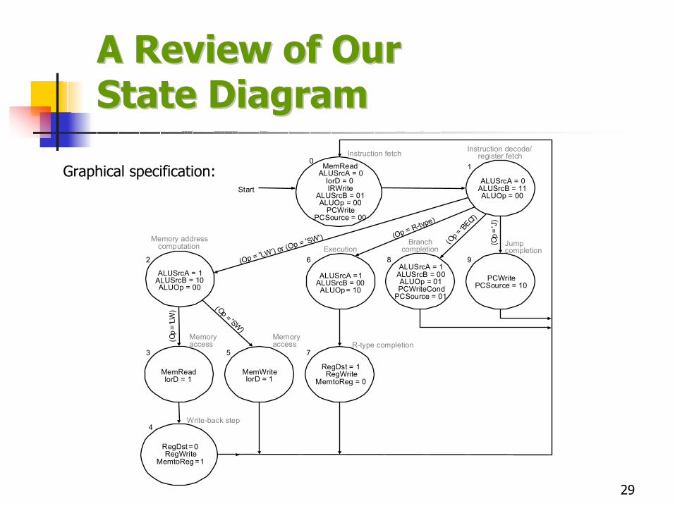
A Review of OurA Review of OurState DiagramState Diagram
PCWritePCSource = 10
ALUSrcA = 1ALUSrcB = 00ALUOp = 01PCWriteCond
PCSource = 01
ALUSrcA =1ALUSrcB = 00ALUOp= 10
RegDst = 1RegWrite
MemtoReg = 0MemWriteIorD = 1
MemReadIorD = 1
ALUSrcA = 1ALUSrcB = 10ALUOp = 00
RegDst =0RegWrite
MemtoReg =1
ALUSrcA = 0ALUSrcB = 11ALUOp = 00
MemReadALUSrcA = 0
IorD = 0IRWrite
ALUSrcB = 01ALUOp = 00
PCWritePCSource = 00
Instruction fetch Instruction decode/register fetch
Jumpcompletion
BranchcompletionExecution
Memory addresscomputation
Memoryaccess
Memoryaccess R-type completion
Write-back step
(Op = 'LW') or (Op = 'SW') (Op = R-type)
(Op = 'BEQ')
(Op
='J'
)
( Op = 'SW')
(Op
='LW
')
4
01
9862
753
Start
Graphical specification:

30
Sequencing: Sequencing: Address Select LogicAddress Select Logic
Dispatch ROM 1Op Opcode name Value
000000 R-format 0110000010 jmp 1001000100 beq 1000100011 lw 0010101011 sw 0010
Dispatch ROM 2Op Opcode name Value
100011 lw 0011101011 sw 0101
State number Address-control action Value of AddrCtl0 Use incremented state 31 Use dispatch ROM 1 12 Use dispatch ROM 2 23 Use incremented state 34 Replace state number by 0 05 Replace state number by 0 06 Use incremented state 37 Replace state number by 0 08 Replace state number by 0 09 Replace state number by 0 0
State
Op
Adder
1
PLA or ROM
Mux3 2 1 0
Dispatch ROM 1Dispatch ROM 2
0
AddrCtl
Address select logic
Instruction registeropcode field

31
A A MicroprogramMicroprogramControl UnitControl Unit
PCWritePCWriteCondIorD
MemtoRegPCSourceALUOpALUSrcBALUSrcARegWrite
AddrCtl
Outputs
Microcode memory
IRWrite
MemReadMemWrite
RegDst
Control unit
Input
Microprogram counter
Address select logicO
p[5–
0]Adder
1
Datapath
Instruction registeropcode field
BWrite
A microprogram control unit controlling the datapathROM or PLA is now microcode memory (control memory)state register is now microprogram counter (µPC)
Sequencer
Microcodestorage
32
A Review ofA Review ofDatapathDatapath & Control& Control
Note the reason for each control signal; also note that we have included the jump instruction
2
2
2

33
1. IR <= Memory[PC]; PC <= PC + 4; (State 0)
2. Instruction Decode (All instructions);A <= Reg[IR[25:21]]; B <= Reg[IR[20:16]]; (State 1)ALUOut <= PC + (sign-extend(IR[15:0]) << 2);
3. Memory address computation (for lw, sw):ALUOut <= A + sign-extend(IR[15:0]); (State 2)
ALU (R-type): ALUOut <= A op B; (State 6)Conditional branch: if (A==B) then PC <= ALUOut; (State 8)Jump: PC <= PC[31:28] || (IR[25:0]<<2); (State 9)
4. For lw or sw instructions (access memory): MDR <= Memory[ALUOut] (State 3) or Memory[ALUOut] <= B; (State 5)For ALU (R-type) instructions (write result to register): Reg[IR[15:11]] <= ALUOut; (State 7)
5. For lw instruction only (write data from MDR to register): Reg[IR[20:16]]<= MDR; (State 4)
A Review of the Instruction A Review of the Instruction Execution StepsExecution Steps

34
A specification methodologyappropriate if hundreds of opcodes, modes, cycles, etc.signals specified symbolically using microinstructionsE.g. Read PC = Read memory using PC as address and write result into IR (& MDR) (see next slide for details)
Our symbolic microprogram with 10 microinstructions:
A Symbolic A Symbolic MicroprogramMicroprogram
LabelALU
control SRC1 SRC2Register control Memory
PCWrite control Sequencing
Fetch Add PC 4 Read PC ALU SeqAdd PC Extshft Read Dispatch 1
Mem1 Add A Extend Dispatch 2LW2 Read ALU Seq
Write MDR FetchSW2 Write ALU FetchRformat1 Func code A B Seq
Write ALU FetchBEQ1 Subt A B ALUOut-cond FetchJUMP1 Jump address Fetch
Microassembler: performs checks to remove combinations that cannot be supported in datapath
35
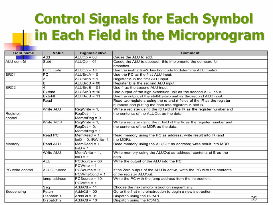
Control Signals for Each Symbol Control Signals for Each Symbol in Each Field in the in Each Field in the MicroprogramMicroprogram
Field name Value Signals active CommentAdd ALUOp = 00 Cause the ALU to add.
ALU control Subt ALUOp = 01 Cause the ALU to subtract; this implements the compare forbranches.
Func code ALUOp = 10 Use the instruction's function code to determine ALU control.SRC1 PC ALUSrcA = 0 Use the PC as the first ALU input.
A ALUSrcA = 1 Register A is the first ALU input.B ALUSrcB = 00 Register B is the second ALU input.
SRC2 4 ALUSrcB = 01 Use 4 as the second ALU input.Extend ALUSrcB = 10 Use output of the sign extension unit as the second ALU input.Extshft ALUSrcB = 11 Use the output of the shift-by-two unit as the second ALU input.Read Read two registers using the rs and rt fields of the IR as the register
numbers and putting the data into registers A and B.Write ALU RegWrite = 1, Write a register using the rd field of the IR as the register number and
Register RegDst = 1, the contents of the ALUOut as the data.control MemtoReg = 0
Write MDR RegWrite = 1, Write a register using the rt field of the IR as the register number andRegDst = 0, the contents of the MDR as the data.MemtoReg = 1
Read PC MemRead = 1, Read memory using the PC as address; write result into IR (and IorD = 0, IRWrite=1 the MDR).
Memory Read ALU MemRead = 1, Read memory using the ALUOut as address; write result into MDR.lorD = 1
Write ALU MemWrite = 1, Write memory using the ALUOut as address, contents of B as thelorD = 1 data.
ALU PCSource = 00 Write the output of the ALU into the PC.PCWrite = 1
PC write control ALUOut-cond PCSource = 01, If the Zero output of the ALU is active, write the PC with the contentsPCWriteCond = 1 of the register ALUOut.
jump address PCSource = 10, Write the PC with the jump address from the instruction.PCWrite = 1
Seq AddrCtl = 11 Choose the next microinstruction sequentially.Sequencing Fetch AddrCtl = 00 Go to the first microinstruction to begin a new instruction.
Dispatch 1 AddrCtl = 01 Dispatch using the ROM 1.Dispatch 2 AddrCtl = 10 Dispatch using the ROM 2.

36
No encoding of control signals in microinstruction format (horizontal microprogram):1 bit for each control signal in datapath operation; e.g. control signals s, t, u, v, w, x, y, z will occupy 8 bits in microinstruction
faster, but requires more memory (logic)
used for Vax 780 — an astonishing 400K of control memory!
Lots of encoding of control signals in microinstruction format (vertical microprogram):E.g. s, t, u, v, w, x, y, z will be encoded in say, 4 bits, with 0000 meaning u = 1 (others = 0), 1010 meaning u = w = 1 (others = 0), etc. I.e. all possible combinations are encoded
send the microinstructions through logic to get control signals
uses less memory, but slower
Select a good trade-off
Microcode implementation: on-chip vs off-chip
Maximally Maximally vsvs Minimally Minimally EncodedEncoded

37
ExceptionsExceptions
Exception: unexpected event from within the processor (e.g. arithmetic overflow)Interrupt: “unexpected” event from outside of the processor (e.g. from an I/O device)
An exception or an interrupt causes an unexpected change in control flow: How does the control unit handle an exception/interrupt?In case of an exception, processor should:
save address of the offending instruction in exception program counter (EPC)indicate the reason for exception in Cause register (status register)transfer control to operating system at some specified address (the OS can then provide some service: taking predefined action in response to overflow or stopping the program & reporting an error). If OS continues program execution, it uses EPC to determine where to restart
Another way is vectored interrupts:the address to which control is transferred is determined by cause of the exception
Exception or interruptEitherHardware malfunctions
ExceptionInternalUsing undefined instruction
ExceptionInternalArithmetic overflow
ExceptionInternalInvoke OS from user program
InterruptExternalI/O device request

38
Exceptions HandlingExceptions Handlingby Control Unitby Control Unit
Control unit:two more control signals: EPCWrite & CauseWrite; also IntCausemodify the mux to PC to 4-way mux to allow exception address to PC (the exception address is OS entry point for exception handling, and is 8000 0180hex for MIPS)
To handle two types of exceptions: undefined instruction & arithmetic overflow
add two states in state diagram to do the above: one when no state is defined for the op value at state 1 (then → state 10), the other when overflow is detected from ALU in state 7 (then → state 11)

39
Chapter SummaryChapter Summary
Part 1:Elements of datapath: instruction subset, resources, clocking methodDatapath for different instruction classesBuilding single-cycle datapath: multiplexors, functional units, control signalsSingle-cycle datapath control unit logic: ALU control, main controlSingle-cycle datapath & control: complete picture, critical path, problems
Part 2:Multi-cycle datapath: approach, additional registers & multiplexors, control signalsBreaking instructions into execution stepsMulti-cycle datapath & control: complete pictureFinite state machine (FSM) (hardwired) control & controller implementationMicroprogramming: control, microinstruction format, controller implementation, symbolic microprogram & its control signals, issuesException Handling

![CS/ECE 250: Computer Architecture Designing a Single Cycle Datapath · 2020. 9. 10. · Datapath for Register-Register Operations • R[rd]](https://img.dokumen.tips/doc/110x75/60a285219322d56d1a13aafb/csece-250-computer-architecture-designing-a-single-cycle-datapath-2020-9-10.jpg)