Embed Size (px)
DESCRIPTION
4304
Citation preview
The University of Texas at Dallas Erik Jonsson School ofEngineering & Computer Science
c� C. D. Cantrell (09/2011)
PROCESSOR DESIGN (1)
• Major steps in designing a processor:
. Datapath design� Instructions⇧ Instruction memory⇧ Instruction fetch and decode⇧ Program counter and adder
� Data⇧ Data memory⇧ Register file⇧ ALU
. Control design� Control signal specification� Implementation⇧ Hardwired⇧Microprogrammed

The University of Texas at Dallas Erik Jonsson School ofEngineering & Computer Science
c� C. D. Cantrell (09/2012)
PROCESSOR DATAPATH
• At the end of every clock cycle, data needed in later cycles must be storedin a state element
. Data needed by subsequent instructions is stored in general-purposeregisters (GPRs) and data memory
� GPRs and data memory are the only state elements needed if allinstructions execute in one clock period
. Multi-cycle implementation:
� Instructions execute in more than one clock cycle� Data needed by one instruction in subsequent clock cycles of its
execution must be stored in special-purpose registers⇧ Instruction register, memory data register
. Pipelined implementation:
� Di↵erent stages of multiple instructions execute simultaneously� Data and control signals needed by each instruction in successive clock
cycles of its execution must be stored in pipeline registers

The University of Texas at Dallas Erik Jonsson School ofEngineering & Computer Science
c� C. D. Cantrell (01/1999)
SEQUENTIAL LOGIC CIRCUITS (1)
• The outputs z1, . . . , zm of a sequential logic circuit depend on:
. The inputs x1, . . . , xn
. Internal logical variables y1, . . . , yr (the present state)
. The next state y⇤1, . . . , y⇤r depends on the inputs and the present state:
y⇤j = hj(x1, . . . , xn, y1, . . . , yr) [j 2 (1 : r)]
• Contrast with a combinational logic circuit, where the outputs depend onlyon the inputs:
zi = fi(x1, . . . , xn) [i 2 (1 : m)]
• For a sequential logic circuit, the outputs depend on the inputs and thepresent state:
zi = gi(x1, . . . , xn, y1, . . . , yr) [i 2 (1 : m)]

The University of Texas at Dallas Erik Jonsson School ofEngineering & Computer Science
c� C. D. Cantrell (09/2011)
D LATCH (1)
• NOR gate implementation of a D latch
Q
C
D
_Q
The University of Texas at Dallas Erik Jonsson School ofEngineering & Computer Science
c� C. D. Cantrell (09/2012)
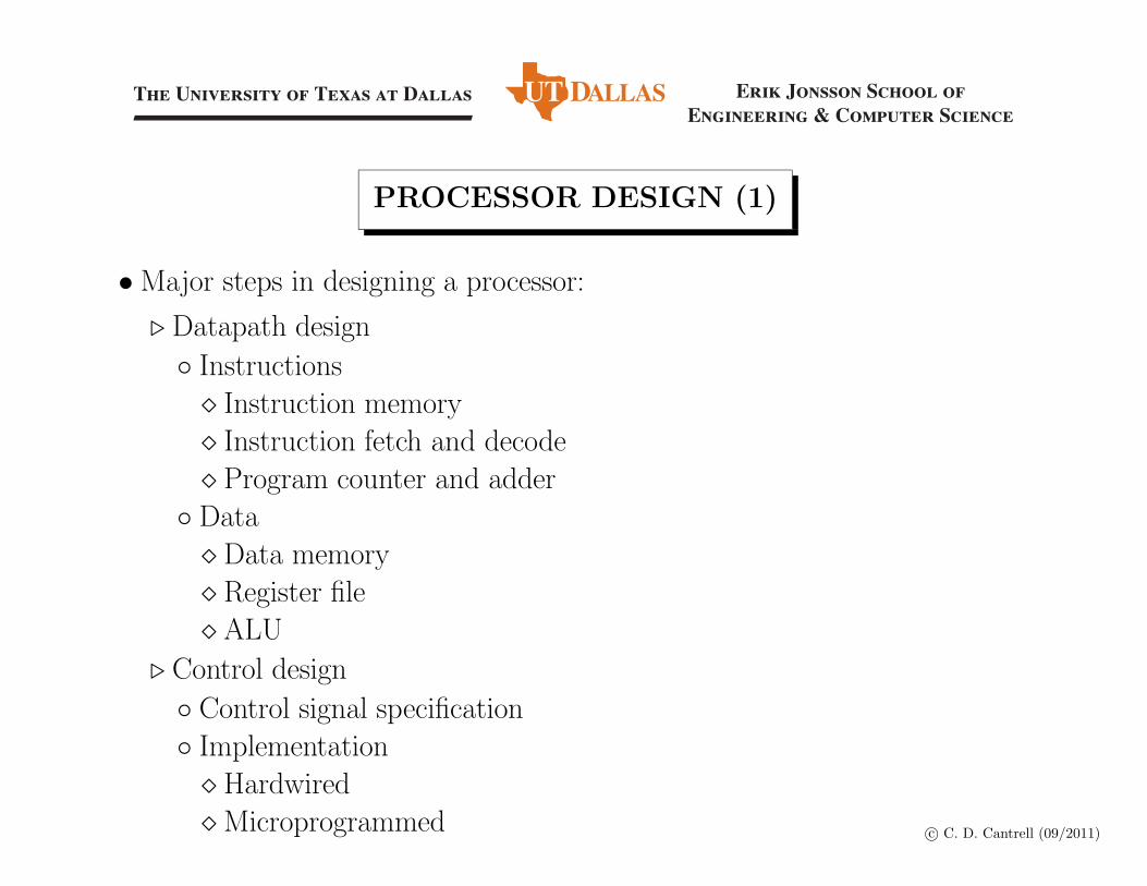
D LATCH (2)
• The state of a D latch is specified uniquely by Q
. Characteristic equation:
Q⇤ = CQ + CD + CDQ = CQ + CD
� Derived from the characteristic equation of the CSR latch(Q⇤ = CQ + CS + CRQ) by setting S = D, R = D
� Can also be derived from excitation table
D Latch Excitation TableInputs Old State Next StateC D Q Q⇤ Comments0 d 0 0 Storage0 d 1 1 of state1 0 d 0 D determines1 1 d 1 next state

The University of Texas at Dallas Erik Jonsson School ofEngineering & Computer Science
c� C. D. Cantrell (01/1999)
SEQUENTIAL LOGIC CIRCUITS (2)
• Hu↵man model of a sequential circuit:
. State element
�Memory that holds the present state� Normally updated at intervals controlled by a clock signal
. Combinational logic that implements the Boolean functionszi (outputs) and y⇤j (next state)
State element
Combinational logic
Clock-controlled update
Inputs Outputs

The University of Texas at Dallas Erik Jonsson School ofEngineering & Computer Science
c� C. D. Cantrell (02/1999)
FINITE STATE MACHINES (1)
• A finite state machine is a conceptual tool used to describe thecomputational functioning of a sequential logic circuit withoutspecifying the implementation
Next-statefunctionCurrent state
Clock
Output function
Next state
Outputs
Inputs

The University of Texas at Dallas Erik Jonsson School ofEngineering & Computer Science
c� C. D. Cantrell (03/1999)
FINITE STATE MACHINES (2)
• A state diagram is a certain kind of directed graph
. The nodes (vertexes) represent states of the machine
� A state is defined by the values of the internal logical variables� Each node in a state diagram is labeled with the values that define the
state that corresponds to the node
. The edges represent the state transitions
� Each edge in a state diagram is labeled with the inputs that cause thestate transition that corresponds to the edge

The University of Texas at Dallas Erik Jonsson School ofEngineering & Computer Science
c� C. D. Cantrell (09/2011)
FINITE STATE MACHINES (3)
• The state diagram for a D latch:
Q = 0
Q = 1
Q = 1
Q = 0
C = 1D = 0
C = 1D = 1C = 0
D = 0,1C = 0
D = 0,1

The University of Texas at Dallas Erik Jonsson School ofEngineering & Computer Science
After David A. Patterson and John L. Hennessy, Computer Organization and Design, 2nd Edition
COMBINATIONAL LOGIC AND STATE ELEMENTS
Clock cycle
Stateelement
1Combinational logic
Stateelement
2
• Every state element has 2 control inputs: Clock signal and write enable

The University of Texas at Dallas Erik Jonsson School ofEngineering & Computer Science
After David A. Patterson and John L. Hennessy, Computer Organization and Design, 2nd Edition
CLOCKING METHODOLOGY
Stateelement Combinational logic
• We assume edge-triggered updating of state elements
. This permits us to read a state element while the clock is asserted, sendthe output through a combinational logic block, and update the stateelement on an edge of the same clock period, with no race conditions
. The designer can choose either a rising or a trailing edge for updating

The University of Texas at Dallas Erik Jonsson School ofEngineering & Computer Science
c� C. D. Cantrell (09/2011)
MASTER-SLAVE D FLIP-FLOP
• The master latch (on the left) receives the D and clock (C) inputs
. When the clock is asserted, the Q output of the master latch follows thedata (D)
. When the clock is deasserted, the master latch is closed, but the second(slave) latch is open
� The output of the slave latch follows its input, which is the output ofthe master latch
_Q
Q
_Q
Dlatch
D
C
Dlatch
DD
C
C
Digital Integrated Circuits © Prentice Hall 1995Sequential Logic
Flip-Flop: Timing Definitions
DATASTABLE
DATASTABLE
In
Out
t
t
t
!
tsetup thold
tpFF

The University of Texas at Dallas Erik Jonsson School ofEngineering & Computer Science
Texas Instruments, Metastable Response in 5-V Logic Circuits, 1997
POSSIBLE OUTPUT SIGNALS IN A METASTABLE STATE
CLK
Q
Q
Q
Expected
Long delay
Anomalous

The University of Texas at Dallas Erik Jonsson School ofEngineering & Computer Science
c� C. D. Cantrell (09/2012)
LIMITS ON CLOCK FREQUENCY
• Delays that determine the minimum clock period (maximum clock frequency):
. Propagation delay through sequential logic blocks, tpFF
. Time for signals to propagate & settle in combinational logic blocks, tcomb
. Setup time, tsetup
. Clock skew, tc
. Clock period T must satisfy
T > tpFF + tcomb + tsetup + tc
Flip-flop Combinationallogic block Flip-flop
D
C
tpFF tcomb tsetup
Q D
C
Q
The University of Texas at Dallas Erik Jonsson School ofEngineering & Computer Science
After David A. Patterson and John L. Hennessy, Computer Organization and Design, 2nd Edition
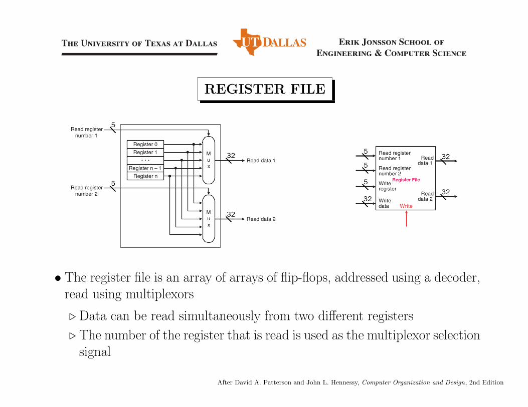
REGISTER FILE
Mux
Register 0Register 1
Register n – 1Register n
Mux
Read data 1
Read data 2
Read registernumber 1
Read registernumber 2
Read registernumber 1 Read
data 1
Readdata 2
Read registernumber 2
Register FileWriteregister
Writedata Write
32
32
5
5
5
5
5
32
32
32
• The register file is an array of arrays of flip-flops, addressed using a decoder,read using multiplexors
. Data can be read simultaneously from two di↵erent registers
. The number of the register that is read is used as the multiplexor selectionsignal

The University of Texas at Dallas Erik Jonsson School ofEngineering & Computer Science
After David A. Patterson and John L. Hennessy, Computer Organization and Design, 2nd Edition
APPLICATION OF DECODER TO REGISTER ADDRESSING
n-to-2n
decoder
Register 0
Register 1
Register 2n – 2C
C
D
D
C
C
D
D
Register number
Write
Register data
0
1
2n – 2
Register 2n – 1
2n – 1
(n bits)
enable
32
n
Data is broadcast to all registers,but only the register selected by
the decoder is modified
• Each register has an “enable” input (labeled C in the figure)
. A register’s enable input must be asserted in order for data to be writtento the register through the “data” input (labeled D)
. The enable input is controlled by an AND gate
. Both the signal from the decoder and the “write enable” signal must beasserted in order for the register’s enable input to be asserted

The University of Texas at Dallas Erik Jonsson School ofEngineering & Computer Science
c� C. D. Cantrell (09/2010)
SINGLE-CYCLE IMPLEMENTATION
• An implementation in which every instruction completes in one clock periodoptimizes one factor in the performance equation, making CPI = 1
CPU execution time =Instructions
Program⇥ Clock periods
Instruction⇥ Seconds
Clock Period
. The number of instructions/program is una↵ected
. However, the duration of a clock period increases so much that the increaseo↵sets the improvement due to CPI = 1
. A single-cycle implementation is useful to study for an understanding ofthe datapath and control signals
. Later, we will study a multi-cycle implementation, which reduces the clockperiod but increases CPI and complicates the datapath & control
. Finally, we will study a pipelined implementation, which reduces both theclock period and CPI
The University of Texas at Dallas Erik Jonsson School ofEngineering & Computer Science
After David A. Patterson and John L. Hennessy, Computer Organization and Design, 4th Edition
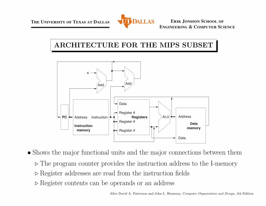
ARCHITECTURE FOR THE MIPS SUBSET
Data
PC Address Instruction
Instructionmemory
Registers ALU Address
Data
Datamemory
AddAdd
4
Register #
Register #
Register #
• Shows the major functional units and the major connections between them
. The program counter provides the instruction address to the I-memory
. Register addresses are read from the instruction fields
. Register contents can be operands or an address

The University of Texas at Dallas Erik Jonsson School ofEngineering & Computer Science
After David A. Patterson and John L. Hennessy, Computer Organization and Design, 4th Edition
IMPLEMENTATION OF THE ARCHITECTURE
Data
PC Address Instruction
Instructionmemory
Registers ALU Address
Data
Datamemory
AddAdd
4
MemWrite
MemRead
Mux
Mux
Mux
Control
RegWrite
Zero
Branch
ALU operation
Register #
Register #
Register #

The University of Texas at Dallas Erik Jonsson School ofEngineering & Computer Science
After David A. Patterson and John L. Hennessy, Computer Organization and Design, 2nd Edition
BUILDING BLOCKS OF THE INSTRUCTION DATAPATH
PC
Instructionmemory
Instructionaddress
Instruction
a. Instruction memory b. Program counter
Add Sum
c. Adder
32
32
32 32
32
32
32
• We need two state elements and an adder (for address computation)
. For pedagogical purposes, the instruction memory is read-only
. The program counter is written at the end of every clock period
� No read/write enable inputs are needed for either state element

The University of Texas at Dallas Erik Jonsson School ofEngineering & Computer Science
After David A. Patterson and John L. Hennessy, Computer Organization and Design, 2nd Edition
DATAPATH FOR INSTRUCTION FETCH
PC
Instructionmemory
Readaddress
Instruction
4
Add
32
32
32
32
32
The University of Texas at Dallas Erik Jonsson School ofEngineering & Computer Science
c� C. D. Cantrell (09/2010)
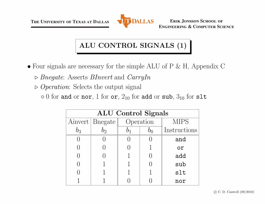
ALU CONTROL SIGNALS (1)
• Four signals are necessary for the simple ALU of P & H, Appendix C
. Bnegate: Asserts BInvert and CarryIn
. Operation: Selects the output signal
� 0 for and or nor, 1 for or, 210 for add or sub, 310 for slt
ALU Control SignalsAinvert Bnegate Operation MIPS
b3 b2 b1 b0 Instructions0 0 0 0 and0 0 0 1 or0 0 1 0 add0 1 1 0 sub0 1 1 1 slt1 1 0 0 nor
The University of Texas at Dallas Erik Jonsson School ofEngineering & Computer Science
After David A. Patterson and John L. Hennessy, Computer Organization and Design, 4th Edition
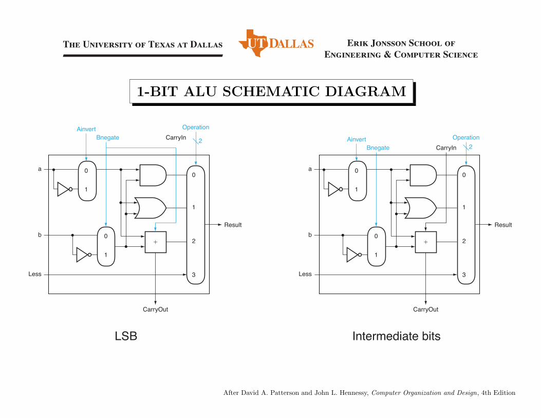
1-BIT ALU SCHEMATIC DIAGRAM
Bnegate
a
b
CarryIn
CarryOut
Operation
1
0
2
Result
1
0
Ainvert
1
0
3Less
Bnegate
a
b
CarryIn
CarryOut
Operation
1
0
2
Result
1
0
Ainvert
1
0
3Less
LSB Intermediate bits
22

The University of Texas at Dallas Erik Jonsson School ofEngineering & Computer Science
c� C. D. Cantrell (09/2011)
ALU CONTROL SIGNALS (2)
• Functions of the ALU control signals for each bit of 32 or 64:
. The value of b1b0 determines which device’s output is selected
� b1b0 = 00 selects the AND output� b1b0 = 01 selects the OR output� b1b0 = 10 selects the SUM output of the adder� b1b0 = 11 selects the Less input⇧ Less is asserted only in the LSB, and only if the Set output of the
ALU for the MSB is 1
. Bnegate selects addition or subtraction by adding the twos complement
� If Bnegate is deasserted, the output of the adder is a + b� If Bnegate is asserted, the adder computes a + b̄ + 1
. The control unit that P&H design does not make use of AInvert

The University of Texas at Dallas Erik Jonsson School ofEngineering & Computer Science
After David A. Patterson and John L. Hennessy, Computer Organization and Design, 4th Edition
MODULES NEEDED FOR R-FORMAT INSTRUCTIONS
Readregister 1
Registers ALUData
Data
ZeroALU
result
RegWrite
a. Registers b. ALU
5
5
5
Registernumbers
Readdata 1
Readdata 2
ALU operation4
Readregister 2WriteregisterWriteData
• The register file can be read and written in the same clock period
. Data written in an earlier clock period is read; data from the current clockperiod is written at the end

The University of Texas at Dallas Erik Jonsson School ofEngineering & Computer Science
After David A. Patterson and John L. Hennessy, Computer Organization and Design, 4th Edition
ADDITIONAL MODULES FOR LOADS AND STORES
Address Readdata
Datamemory
a. Data memory unit
Writedata
MemRead
MemWrite
b. Sign extension unit
Sign-extend
16 32
• The data memory unit needs separate read and write signals
. The sign extension unit is necessary in order to convert a 16-bit immediatevalue to a 32-bit relative address

The University of Texas at Dallas Erik Jonsson School ofEngineering & Computer Science
After David A. Patterson and John L. Hennessy, Computer Organization and Design, 2nd Edition
DATAPATH FOR R-FORMAT INSTRUCTIONS
Instruction
Register fileWriteregister
Readdata 1
Readdata 2
Readregister 1
Readregister 2
Writedata
ALUresult
ALUZero
RegWrite
ALU control432
32
32
5
5
5
Op
Rs
Rt
Rd
Shamt
Funct6
55
55
6

The University of Texas at Dallas Erik Jonsson School ofEngineering & Computer Science
c� C. D. Cantrell (12/1999)
R-FORMAT DATAPATH: EXAMPLE (1)
• Show the hexadecimal values of all datapath signals for the instruction
add $5,$4,$3
. The values in the registers read are:
� ($3) = 410
� ($4) = �1310
• Results are shown in the following slide

The University of Texas at Dallas Erik Jonsson School ofEngineering & Computer Science
c� C. D. Cantrell (12/1999)
R-FORMAT DATAPATH: EXAMPLE (2)
Register fileWriteregister
Readdata 1
Readdata 2
Readregister 1
Readregister 2
Writedata
ALUresult
ALUZero
Instruction
Op
Rs
Rt
Rd
Shamt
Funct6
55
55
6
0x04
0x03
0x05
0xFFFFFFF3
0x00000004
0xFFFFFFF7

The University of Texas at Dallas Erik Jonsson School ofEngineering & Computer Science
After David A. Patterson and John L. Hennessy, Computer Organization and Design, 2nd Edition
MODULES NEEDED FOR LOADS AND STORES
16 32Sign
extend
b. Sign-extension unit
MemRead
MemWrite
Data
memoryWritedata
Readdata
a. Data memory unit
Address32
32
32

The University of Texas at Dallas Erik Jonsson School ofEngineering & Computer Science
After David A. Patterson and John L. Hennessy, Computer Organization and Design, 2nd Edition
DATAPATH FOR LOADS
16 32
Registers
Writeregister
Readdata 1
Readregister 1
Datamemory
Writedata
Readdata
Writedata
Signextend
ALUresult
ZeroALU
Address
MemRead
RegWrite
ALU operation4
32
32
32
5
5
Register Access Address Computation Memory Read
Instruction
Op
Rs
Rt
Imm
65
516
The University of Texas at Dallas Erik Jonsson School ofEngineering & Computer Science
c� C. D. Cantrell (12/1999)
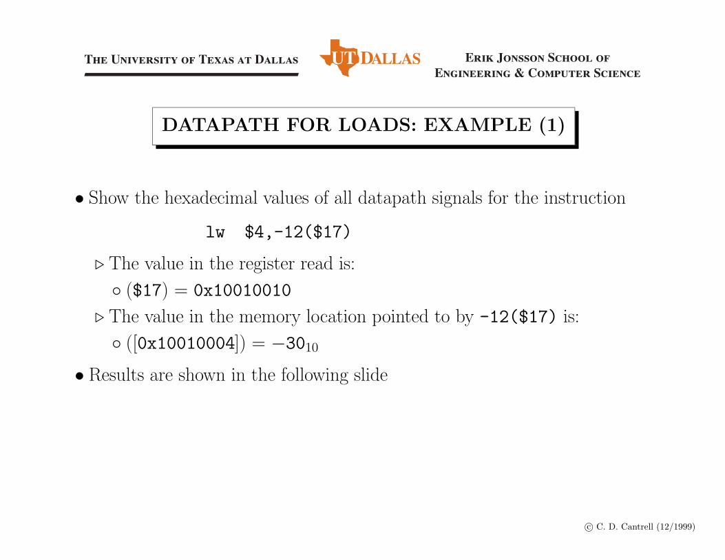
DATAPATH FOR LOADS: EXAMPLE (1)
• Show the hexadecimal values of all datapath signals for the instruction
lw $4,-12($17)
. The value in the register read is:
� ($17) = 0x10010010
. The value in the memory location pointed to by -12($17) is:
� ([0x10010004]) = �3010
• Results are shown in the following slide
The University of Texas at Dallas Erik Jonsson School ofEngineering & Computer Science
c� C. D. Cantrell (12/1999)
DATAPATH FOR LOADS: EXAMPLE (2)
InstructionRegisters
Writeregister
Readdata 1
Readdata 2
Readregister 1
Readregister 2
Datamemory
Writedata
Readdata
Writedata
Signextend
ALUresult
ZeroALU
Address
MemRead
MemWrite
RegWrite
ALU operation4
Register Access Address Computation Memory Read or Write
0x11
0x04
0xFFF4 0xFFFFFFF4
0x10010010
0x10010004
0xFFFFFFE2

The University of Texas at Dallas Erik Jonsson School ofEngineering & Computer Science
After David A. Patterson and John L. Hennessy, Computer Organization and Design, 2nd Edition
DATAPATH FOR STORES
16 32
Registers
Readregister 2
Readdata 1
Readdata 2
Readregister 1
Datamemory
Writedata
Readdata
Writedata
Signextend
ALUresult
ZeroALU
Address
MemWrite
ALU operation4
32
32
32
5
5
Register Access Address Computation Memory Write
Instruction
Op
Rs
Rt
Imm
65
516
The University of Texas at Dallas Erik Jonsson School ofEngineering & Computer Science
After David A. Patterson and John L. Hennessy, Computer Organization and Design, 2nd Edition
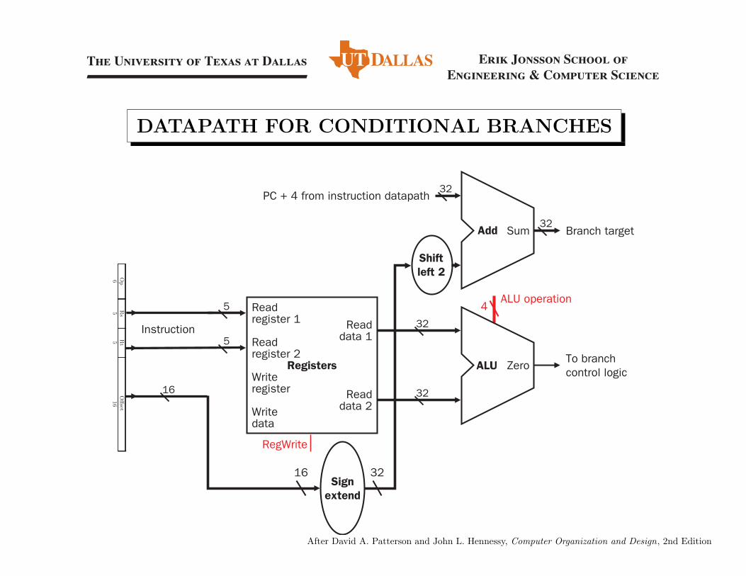
DATAPATH FOR CONDITIONAL BRANCHES
16 32Sign
extend
ZeroALU
Sum
To branchcontrol logic
Branch target
PC + 4 from instruction datapath
Instruction
Add
RegistersWriteregister
Readdata 1
Readdata 2
Readregister 1
Readregister 2
Writedata
RegWrite
ALU operation4
32
32
32
32
5
5
Op
Rs
Rt
Offset
65
516
16
Shiftleft 2

The University of Texas at Dallas Erik Jonsson School ofEngineering & Computer Science
After David A. Patterson and John L. Hennessy, Computer Organization and Design, 2nd Edition
DATAPATH FOR A JUMP OR JUMP AND LINK
26
ALU
Shiftleft 2 Branch target
Instruction[25-0]
RegistersWriteregister
Readdata 1
Readdata 2
Readregister 1
Readregister 2
Writedata
PCOp
Target
626PC
Add
4
28
PC+4 [31-28]
Jump address[31-0]

The University of Texas at Dallas Erik Jonsson School ofEngineering & Computer Science
c� C. D. Cantrell (09/2010)
DESIGNING A SINGLE DATAPATH
• We will design the simplest possible datapath
. All instructions will complete in one clock period
� No resource can be used more than once in a clock period� Any element needed more than once must be duplicated� Therefore, we need separate instruction and data memories (Harvard
architecture)⇧ In a real design, I-cache and D-cache may be separate⇧Main memory is used for both instructions and data
� Elements that are needed by di↵erent classes of instructions can beshared⇧We use multiplexors to select among multiple connections to the in-
puts of some elements⇧ Control of the multiplexors will require additional control signals
. We do not need a separate instruction register, since the instruction isaccessed at the beginning of the clock period

The University of Texas at Dallas Erik Jonsson School ofEngineering & Computer Science
c� C. D. Cantrell (09/2010)
SUPPORT FOR ALU OPERATIONS, LOADS AND STORES
• In order to choose between di↵erent data sources, we need 2 new multiplexorsand 2 new control signals
. The ALUSrc signal controls a multiplexor that selects the source of datafor one input of the ALU
� The source for and, or, add, sub, slt, and nor is the contents of aregister� The source for lw and sw is a sign-extended immediate value
. The MemtoReg signal controls a multiplexor that selects the source ofdata written back to a register
� One source is the output (i.e., the result of and, etc.)� The other source is a data memory location (for support of lw)
• Other necessary control signals are RegWrite and MemRead and MemWrite
• Don’t confuse the ALUOp control signal with the Opcode field!
. ALUOp is determined from the Opcode field of the instruction

The University of Texas at Dallas Erik Jonsson School ofEngineering & Computer Science
After David A. Patterson and John L. Hennessy, Computer Organization and Design, 2nd Edition
COMBINED ALU/LOAD/STORE DATAPATH
Instruction
16 32
RegistersWriteregister
Readdata 1
Readdata 2
Readregister 1
Readregister 2
Datamemory
Writedata
Readdata
Mux
MuxWrite
data
Signextend
ALUresult
ZeroALU
Address
RegWrite
ALU operation4
MemRead
MemWrite
ALUSrcMemtoReg
32
32
32
32
32
32
5
5
5 32

The University of Texas at Dallas Erik Jonsson School ofEngineering & Computer Science
After David A. Patterson and John L. Hennessy, Computer Organization and Design, 2nd Edition
COMBINED FETCH/ALU/LOAD/STORE DATAPATH
PC
Instructionmemory
Readaddress
Instruction
16 32
Registers
Writeregister
Writedata
Readdata 1
Readdata 2
Readregister 1Readregister 2
Signextend
ALUresult
Zero
Datamemory
Address
Writedata
Readdata M
ux
4
Add
Mux
ALU
RegWrite
ALU operation4
MemRead
MemWrite
ALUSrcMemtoReg32
32
32
32
32
32
32
32
5
5
5
The University of Texas at Dallas Erik Jonsson School ofEngineering & Computer Science
c� C. D. Cantrell (09/2010)
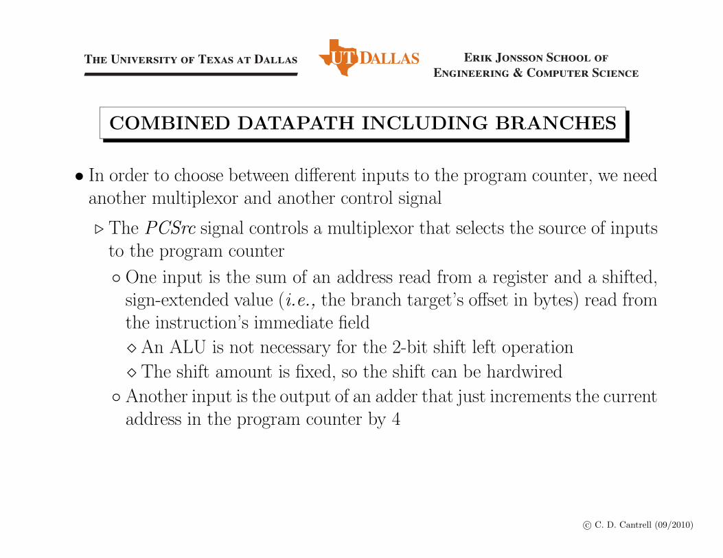
COMBINED DATAPATH INCLUDING BRANCHES
• In order to choose between di↵erent inputs to the program counter, we needanother multiplexor and another control signal
. The PCSrc signal controls a multiplexor that selects the source of inputsto the program counter
� One input is the sum of an address read from a register and a shifted,sign-extended value (i.e., the branch target’s o↵set in bytes) read fromthe instruction’s immediate field⇧ An ALU is not necessary for the 2-bit shift left operation⇧ The shift amount is fixed, so the shift can be hardwired
� Another input is the output of an adder that just increments the currentaddress in the program counter by 4

The University of Texas at Dallas Erik Jonsson School ofEngineering & Computer Science
After David A. Patterson and John L. Hennessy, Computer Organization and Design, 2nd Edition
FETCH/ALU/LOAD/STORE/BRANCH DATAPATH
PC
Instructionmemory
Readaddress
Instruction
16 32
Add ALUresult
Mux
Registers
WriteregisterWritedata
Readdata 1
Readdata 2
Readregister 1Readregister 2
4
Mux
ALU operation4
RegWrite
MemRead
MemWrite
PCSrc
ALUSrc
MemtoReg
ALUresult
ZeroALU
Datamemory
Address
Writedata
Readdata M
ux
Signextend
Add
32
32
3232
5
5
5
32
32
32
32
32
Shiftleft 2

The University of Texas at Dallas Erik Jonsson School ofEngineering & Computer Science
c� C. D. Cantrell (09/2010)
SUPPORT FOR WRITING TO A REGISTER
• In order to select the destination of data written to the register file, we needanother multiplexor and another control signal
. The RegDst signal controls a multiplexor that selects the number of theregister that is written
� The destination register number for an R-format instruction such asadd $rd, $rs, $rt comes from the Rd field in the instruction
� The destination register number for an instruction such aslw $rt, offset($rs) comes from the Rt field in the instruction

The University of Texas at Dallas Erik Jonsson School ofEngineering & Computer Science
After David A. Patterson and John L. Hennessy, Computer Organization and Design, 2nd Edition
DATAPATH WITH CONTROL LINES IDENTIFIED
MemtoReg
MemRead
MemWrite
ALUOp
ALUSrc
RegDst
PC
Instructionmemory
Readaddress
Instruction[31–0]
Instruction [20–16]
Instruction [25–21]
Add
Instruction [5–0]
RegWrite
4
16 32Instruction [15–0]
0Registers
WriteregisterWritedata
Writedata
Readdata 1
Readdata 2
Readregister 1Readregister 2
Signextend
ALUresult
Zero
Datamemory
Address Readdata M
ux
1
0
Mux
1
0
Mux
1
0
Mux
1
Instruction [15–11]
ALUcontrol
Shiftleft 2
PCSrc
ALU
Add ALUresult
The University of Texas at Dallas Erik Jonsson School ofEngineering & Computer Science
c� C. D. Cantrell (09/2010)
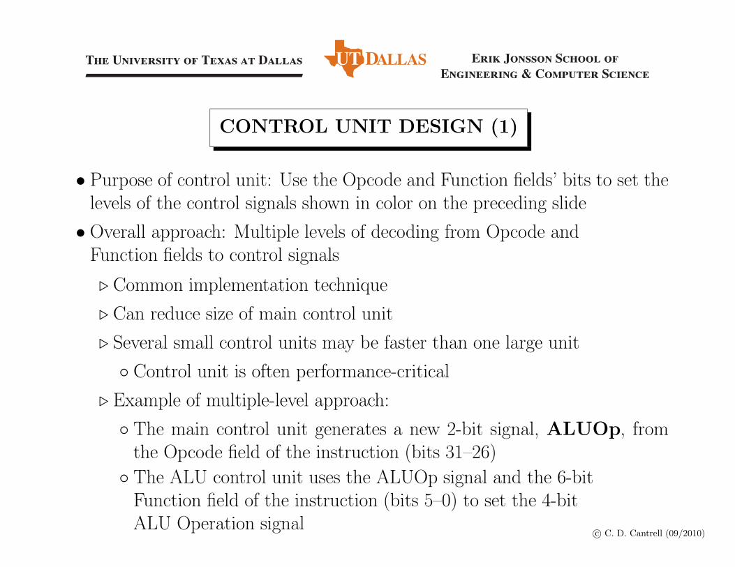
CONTROL UNIT DESIGN (1)
• Purpose of control unit: Use the Opcode and Function fields’ bits to set thelevels of the control signals shown in color on the preceding slide
• Overall approach: Multiple levels of decoding from Opcode andFunction fields to control signals
. Common implementation technique
. Can reduce size of main control unit
. Several small control units may be faster than one large unit
� Control unit is often performance-critical
. Example of multiple-level approach:
� The main control unit generates a new 2-bit signal, ALUOp, fromthe Opcode field of the instruction (bits 31–26)� The ALU control unit uses the ALUOp signal and the 6-bit
Function field of the instruction (bits 5–0) to set the 4-bitALU Operation signal

The University of Texas at Dallas Erik Jonsson School ofEngineering & Computer Science
After David A. Patterson and John L. Hennessy, Computer Organization and Design, 4th Edition
INSTRUCTION FORMATS
Field rs rt rd shamt funct
Bit positions 31:26 25:21 20:16 15:11 10:6 5:0
a. R-type instruction
Field 35 or 43 rs rt address
Bit positions 31:26 25:21 20:16 15:0
b. Load or store instruction
Field 4 rs rt address
Bit positions 31:26 25:21 20:16 15:0
c. Branch instruction
Field 000010 address
Bit positions 31:26 25:0
d. Jump instruction
opcode=0

The University of Texas at Dallas Erik Jonsson School ofEngineering & Computer Science
c� C. D. Cantrell (09/2010)
DETAILED INSTRUCTION FORMATS (1)
add Rd, Rs, Rt Addition (with overflow)
0 Rs Rt Rd 0 0x206 5 5 5 5 6
sub Rd, Rs, Rt Subtract (with overflow)
0 Rs Rt Rd 0 0x226 5 5 5 5 6
and Rd, Rs, Rt and
0 Rs Rt Rd 0 0x246 5 5 5 5 6
or Rd, Rs, Rt or
0 Rs Rt Rd 0 0x256 5 5 5 5 6
The University of Texas at Dallas Erik Jonsson School ofEngineering & Computer Science
c� C. D. Cantrell (09/2010)
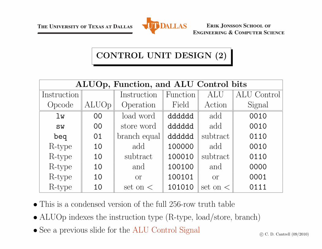
CONTROL UNIT DESIGN (2)
ALUOp, Function, and ALU Control bitsInstruction Instruction Function ALU ALU Control
Opcode ALUOp Operation Field Action Signallw 00 load word dddddd add 0010sw 00 store word dddddd add 0010beq 01 branch equal dddddd subtract 0110
R-type 10 add 100000 add 0010R-type 10 subtract 100010 subtract 0110R-type 10 and 100100 and 0000R-type 10 or 100101 or 0001R-type 10 set on < 101010 set on < 0111
• This is a condensed version of the full 256-row truth table
• ALUOp indexes the instruction type (R-type, load/store, branch)
• See a previous slide for the ALU Control Signal

The University of Texas at Dallas Erik Jonsson School ofEngineering & Computer Science
c� C. D. Cantrell (09/2010)
CONTROL UNIT DESIGN (3)
Truth Table for ALU Control bitsALUOp Function field
ALUOp1 ALUOp0 F5 F4 F3 F2 F1 F0 ALU Control0 0 d d d d d d 0010d 1 d d d d d d 01101 d d d 0 0 0 0 00101 d d d 0 0 1 0 01101 d d d 0 1 0 0 00001 d d d 0 1 0 1 00011 d d d 1 0 1 0 0111
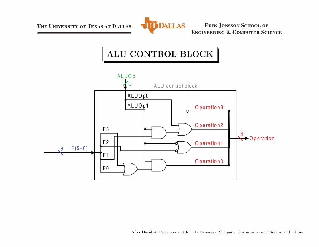
• The “don’t cares” (d) indicate signals that don’t have to be used as inputs tothe AND level of the ALU Control Block, which implements the 3 Booleanfunctions Operation(2–0) (ALU Control (2–0))

The University of Texas at Dallas Erik Jonsson School ofEngineering & Computer Science
c� C. D. Cantrell (09/2010)
EXAMPLES OF ALU CONTROL SIGNALS
Instruction Fields and Control SignalsOpcode Instruction ALUOp Function ALU Control000000 add 10 100000 0010000000 addu 10 100001 0011000000 sub 10 100010 0110000000 slt 10 101010 0111100011 lw 00 dddddd 0010101011 sw 00 dddddd 0010000100 beq 01 dddddd 0110
• ALUOp indexes the instruction type (R-type, load/store, branch)
The University of Texas at Dallas Erik Jonsson School ofEngineering & Computer Science
After David A. Patterson and John L. Hennessy, Computer Organization and Design, 2nd Edition
ALU CONTROL BLOCK
O p e ra tio n 2
O p e ra tio n 1
O p e ra tio n 0
O p e ra tio n
A L U O p1
F3
F2
F1
F0
F(5–0)
A L U O p0
A LU O p
AL U con tro l b lock
6
2
4
0O p e ra tio n 3

The University of Texas at Dallas Erik Jonsson School ofEngineering & Computer Science
After David A. Patterson and John L. Hennessy, Computer Organization and Design, 4th Edition
SIMPLE DATAPATH WITH CONTROL LINES
Readregister 1
Writedata
Registers
ALU
Add
Zero
MemRead
MemWrite
RegWrite
PCSrc
MemtoRegRead
data 1
Readdata 2
Sign-extend
16 32
Instruction[31:0] ALU
result
AddALU
result
MuxMux
Mux
ALUSrc
Address
Datamemory
Readdata
Shiftleft 2
4
Readaddress
Instructionmemory
PC
1
0
0
1
0
1
Mux
0
1
ALUcontrol
ALUOpInstruction [5:0]
Instruction [25:21]
Instruction [15:11]
Instruction [20:16]
Instruction [15:0]
RegDst
Readregister 2Writeregister
Writedata

The University of Texas at Dallas Erik Jonsson School ofEngineering & Computer Science
c� C. D. Cantrell (09/2010)
DETAILED INSTRUCTION FORMATS (2)
lw Rt, address|Offset(Base) Load Word
0x23 Base Rt O↵set6 5 5 16
sw Rt, address Store Word
0x2b Rs Rt O↵set6 5 5 16
beq Rs, Rt, label Branch on Equal
4 Rs Rt O↵set6 5 5 16

The University of Texas at Dallas Erik Jonsson School ofEngineering & Computer Science
After David A. Patterson and John L. Hennessy, Computer Organization and Design, 4th Edition
EFFECTS OF THE CONTROL SIGNALS
Signal name Effect when deasserted Effect when asserted
RegDst The register destination number for the Write register comes from the rt fi eld (bits 20:16).
The register destination number for the Write register comes from the rd fi eld (bits 15:11).
RegWrite None. The register on the Write register input is written with the value on the Write data input.
ALUSrc The second ALU operand comes from the second register fi le output (Read data 2).
The second ALU operand is the sign-extended, lower 16 bits of the instruction.
PCSrc The PC is replaced by the output of the adder that computes the value of PC + 4.
The PC is replaced by the output of the adder that computes the branch target.
MemRead None. Data memory contents designated by the address input are put on the Read data output.
MemWrite None. Data memory contents designated by the address input are replaced by the value on the Write data input.
MemtoReg The value fed to the register Write data input comes from the ALU.
The value fed to the register Write data input comes from the data memory.
Branch The instruction is not beq; no branch. The instruction is beq; branch if Zero=1.

The University of Texas at Dallas Erik Jonsson School ofEngineering & Computer Science
After David A. Patterson and John L. Hennessy, Computer Organization and Design, 2nd Edition
SIMPLE DATAPATH WITH CONTROL UNIT
PC
Instructionmemory
Readaddress
Instruction[31–0]
Instruction [20 16]
Instruction [25 21]
Add
Instruction [5 0]
MemtoRegALUOpMemWrite
RegWrite
MemReadBranchRegDst
ALUSrc
Instruction [31 26]
4
16 32Instruction [15 0]
0
0Mux
0
1
Control
Add ALUresult
Mux
0
1
RegistersWriteregister
Writedata
Readdata 1
Readdata 2
Readregister 1
Readregister 2
Signextend
Mux1
ALUresult
Zero
PCSrc
Datamemory
Writedata
Readdata
Mux
1
Instruction [15 11]
ALUcontrol
Shiftleft 2
ALUAddress
2
4
2
6
5
5
532
32
32
32
32
32
32

The University of Texas at Dallas Erik Jonsson School ofEngineering & Computer Science
c� C. D. Cantrell (09/2010)
SETTINGS OF CONTROL LINES
Inst. Reg ALU Mem- Reg Mem Mem Br ALUOptype Dst Src to-reg. Wr Rd Wr bit 1 bit 0
R-type 1 0 0 1 0 0 0 1 0lw 0 1 1 1 1 0 0 0 0sw d 1 d 0 0 1 0 0 0beq d 0 d 0 0 0 1 0 1
• For R-type instructions, data sources are $rs, $rt; destination is $rd
. RegDst, RegWr are set; ALUSrc is cleared
. The ALU control signal is set from the Funct field of the instruction
• PCSrc cannot be set solely from the table
. When Branch is cleared, PC 7! PC + 4
. When Branch is set and Zero is asserted, PC 7! branch target

The University of Texas at Dallas Erik Jonsson School ofEngineering & Computer Science
After David A. Patterson and John L. Hennessy, Computer Organization and Design, 2nd Edition
COMBINATIONAL LOGIC IMPLEMENTATION
R-format Iw sw beq
Op0Op1Op2Op3Op4Op5
Inputs
Outputs
RegDst
ALUSrcMemtoRegRegWriteMemReadMemWriteBranchALUOp1ALUOp0
Op
Rs
Rt
Rd
Shamt
Funct6
55
55
6
Operation2
Operation1
Operation0
Operation
ALUOp1
F3
F2
F1
F0
F(5–0)
ALUOp0
ALUOpALU control block
6
2
4
0 Operation3

The University of Texas at Dallas Erik Jonsson School ofEngineering & Computer Science
c� C. D. Cantrell (09/2010)
DETAILED INSTRUCTION FORMATS (1)
add Rd, Rs, Rt Addition (with overflow)
0 Rs Rt Rd 0 0x206 5 5 5 5 6
sub Rd, Rs, Rt Subtract (with overflow)
0 Rs Rt Rd 0 0x226 5 5 5 5 6
and Rd, Rs, Rt and
0 Rs Rt Rd 0 0x246 5 5 5 5 6
or Rd, Rs, Rt or
0 Rs Rt Rd 0 0x256 5 5 5 5 6

The University of Texas at Dallas Erik Jonsson School ofEngineering & Computer Science
After David A. Patterson and John L. Hennessy, Computer Organization and Design, 2nd Edition
DATA AND CONTROL SIGNALS FOR add $5, $4, $3
PC
Instructionmemory
Readaddress
Instruction[31–0]
Instruction [20 16]
Instruction [25 21]
Add
Instruction [5 0]
MemtoRegALUOpMemWrite
RegWrite
MemReadBranchRegDst
ALUSrc
Instruction [31 26]
4
16 32Instruction [15 0]
0
0Mux
0
1
Control
Add ALUresult
Mux
0
1
RegistersWriteregister
Writedata
Readdata 1
Readdata 2
Readregister 1
Readregister 2
Signextend
Mux1
ALUresult
Zero
PCSrc
Datamemory
Writedata
Readdata
Mux
1
Instruction [15 11]
ALUcontrol
Shiftleft 2
ALUAddress
2
4
2
6
5
5
532
32
32
32
32
32
32
000
1000
1
10
00
0
0
0
0
0010
10
0
1
000000
00100
00011
00101
1000000xFFFFFFF7
($4) = Read data 1: 0xFFFFFFF3($3) = Read data 2: 0x00000004
0xFFFFFFF7
PC+4PC+4
PC+4

The University of Texas at Dallas Erik Jonsson School ofEngineering & Computer Science
After David A. Patterson and John L. Hennessy, Computer Organization and Design, 2nd Edition
PHASE 1 OF R-TYPE EXECUTION
PC
Instructionmemory
Readaddress
Instruction[31–0]
Instruction [20–16]
Instruction [25–21]
Add
Instruction [5–0]
MemtoRegALUOpMemWrite
RegWrite
MemReadBranchRegDst
ALUSrc
Instruction [31–26]
4
16 32Instruction [15–0]
0
0Mux
0
1
Control
Add ALUresult
Mux
0
1
RegistersWriteregister
Writedata
Readdata 1
Readdata 2
Readregister 1
Readregister 2
Signextend
Shiftleft 2
Mux1
ALUresult
Zero
Datamemory
Writedata
Readdata
Mux
1
Instruction [15–11]
ALUcontrol
ALUAddress
The University of Texas at Dallas Erik Jonsson School ofEngineering & Computer Science
After David A. Patterson and John L. Hennessy, Computer Organization and Design, 2nd Edition
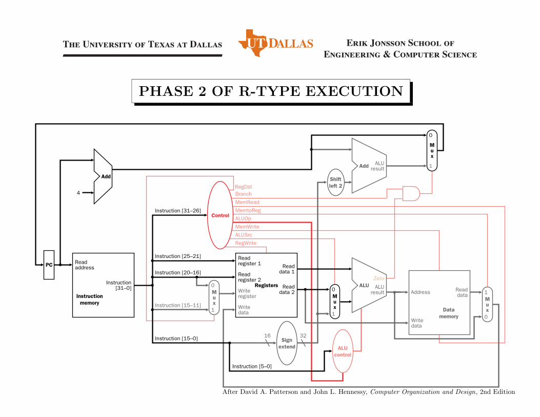
PHASE 2 OF R-TYPE EXECUTION
PC
Instructionmemory
Readaddress
Instruction[31–0]
Instruction [20–16]
Instruction [25–21]
Add
Instruction [5–0]
MemtoRegALUOpMemWrite
RegWrite
MemReadBranchRegDst
ALUSrc
Instruction [31–26]
4
16 32Instruction [15–0]
0
0Mux
0
1
Control
Add ALUresult
Mux
0
1
RegistersWriteregister
Writedata
Readdata 1
Readdata 2
Readregister 1
Readregister 2
Signextend
Shiftleft 2
Mux1
ALUresult
Zero
Datamemory
Writedata
Readdata
Mux
1
Instruction [15–11]
ALUcontrol
ALUAddress

The University of Texas at Dallas Erik Jonsson School ofEngineering & Computer Science
After David A. Patterson and John L. Hennessy, Computer Organization and Design, 2nd Edition
PHASE 3 OF R-TYPE EXECUTION
PC
Instructionmemory
Readaddress
Instruction[31–0]
Instruction [20 16]
Instruction [25 21]
Add
Instruction [5 0]
MemtoRegALUOpMemWrite
RegWrite
MemReadBranchRegDst
ALUSrc
Instruction [31 26]
4
16 32Instruction [15 0]
0
0Mux
0
1
ALUcontrol
Control
Add ALUresult
Mux
0
1
RegistersWriteregister
Writedata
Readdata 1
Readdata 2
Readregister 1
Readregister 2
Signextend
Mux1
ALUresult
Zero
Datamemory
ReaddataAddress
Writedata
Mux
1
Instruction [15 11]
ALU
Shiftleft 2

The University of Texas at Dallas Erik Jonsson School ofEngineering & Computer Science
After David A. Patterson and John L. Hennessy, Computer Organization and Design, 2nd Edition
PHASE 4 OF R-TYPE EXECUTION
PC
Instructionmemory
Readaddress
Instruction[31–0]
Instruction [20 16]
Instruction [25 21]
Add
Instruction [5 0]
MemtoRegALUOpMemWrite
RegWrite
MemReadBranchRegDst
ALUSrc
Instruction [31 26]
4
16 32Instruction [15 0]
0
0Mux
0
1
ALUcontrol
Control
Shiftleft 2
Add ALUresult
Mux
0
1
RegistersWriteregister
Writedata
Readdata 1
Readdata 2
Readregister 1
Readregister 2
Signextend
Mux1
ALUresult
Zero
Datamemory
Writedata
Readdata
Mux
1
Instruction [15 11]
ALUAddress

The University of Texas at Dallas Erik Jonsson School ofEngineering & Computer Science
c� C. D. Cantrell (09/2010)
DETAILED INSTRUCTION FORMATS (2)
lw Rt, address|Offset(Base) Load Word
0x23 Base Rt O↵set6 5 5 16
sw Rt, address Store Word
0x2b Rs Rt O↵set6 5 5 16
beq Rs, Rt, label Branch on Equal
4 Rs Rt O↵set6 5 5 16

The University of Texas at Dallas Erik Jonsson School ofEngineering & Computer Science
After David A. Patterson and John L. Hennessy, Computer Organization and Design, 2nd Edition
DATA AND CONTROL SIGNALS FOR lw $4,-12($17)
PC
Instructionmemory
Readaddress
Instruction[31–0]
Instruction [20 16]
Instruction [25 21]
Add
Instruction [5 0]
MemtoRegALUOpMemWrite
RegWrite
MemReadBranchRegDst
ALUSrc
Instruction [31 26]
4
16 32Instruction [15 0]
0
0Mux
0
1
Control
Add ALUresult
Mux
0
1
RegistersWriteregister
Writedata
Readdata 1
Readdata 2
Readregister 1
Readregister 2
Signextend
Mux1
ALUresult
Zero
PCSrc
Datamemory
Writedata
Readdata
Mux
1
Instruction [15 11]
ALUcontrol
Shiftleft 2
ALUAddress
2
4
2
6
5
5
532
32
32
32
32
32
32
011
0001
1
00
00
0
1
1
1
0010
00
0
0
100011
10001
00100
0xFFF4
($17) = Read data 1: 0x10010010Sign extender output: 0xFFFFFFF4
PC+4PC+4
PC+4
dddddd
1
ALU result: 0x10010004
1

The University of Texas at Dallas Erik Jonsson School ofEngineering & Computer Science
After David A. Patterson and John L. Hennessy, Computer Organization and Design, 2nd Edition
OPERATION OF A LOAD INSTRUCTION
PC
Instructionmemory
Readaddress
Instruction[31–0]
Instruction [15–11]
Instruction [20–16]
Instruction [25–21]
Add
Instruction [5–0]
MemtoRegALUOpMemWrite
RegWrite
MemReadBranchRegDst
ALUSrc
Instruction [31–26]
4
16 32Instruction [15–0]
0
0Mux
0
1
ALUcontrol
Control
Shiftleft 2
Add ALUresult
Mux
0
1
RegistersWriteregister
Writedata
Readdata 1
Readdata 2
Readregister 1
Readregister 2
Signextend
Mux1
ALUresult
Zero
Datamemory
Writedata
Readdata
Mux
1ALU
Address

The University of Texas at Dallas Erik Jonsson School ofEngineering & Computer Science
After David A. Patterson and John L. Hennessy, Computer Organization and Design, 2nd Edition
DATA AND CONTROL SIGNALS FOR beq $13, $0, 1
PC
Instructionmemory
Readaddress
Instruction[31–0]
Instruction [20 16]
Instruction [25 21]
Add
Instruction [5 0]
MemtoRegALUOpMemWrite
RegWrite
MemReadBranchRegDst
ALUSrc
Instruction [31 26]
4
16 32Instruction [15 0]
0
0Mux
0
1
Control
Add ALUresult
Mux
0
1
RegistersWriteregister
Writedata
Readdata 1
Readdata 2
Readregister 1
Readregister 2
Signextend
Mux1
ALUresult
Zero
PCSrc
Datamemory
Writedata
Readdata
Mux
1
Instruction [15 11]
ALUcontrol
Shiftleft 2
ALUAddress
2
4
2
6
5
5
532
32
32
32
32
32
32
10d
0100
0
d1
11
0
d
0
0
0110
01
1
d
000100
01101
00000
0x0001
($13) = Read data 1: 0x00000000Sign extender output: 0x00000001Left shift output: 0x00000004Branch ALU result: PC+8
PC+8PC+4
PC+8
dddddd
0 d
PC+4 PC+8

The University of Texas at Dallas Erik Jonsson School ofEngineering & Computer Science
After David A. Patterson and John L. Hennessy, Computer Organization and Design, 2nd Edition
OPERATION OF A BRANCH INSTRUCTION
PC
Instructionmemory
Readaddress
Instruction[31–0]
Instruction [15–11]
Instruction [20–16]
Instruction [25–21]
Add
Instruction [5–0]
MemtoRegALUOpMemWrite
RegWrite
MemReadBranchRegDst
ALUSrc
Instruction [31–26]
4
16 32Instruction [15–0]
Shiftleft 2
0Mux
0
1
ALUcontrol
Control
RegistersWriteregister
Writedata
Readdata 1
Readregister 1
Readregister 2
Signextend
1
ALUresult
Zero
Datamemory
Writedata
ReaddataM
ux
Readdata 2
Add ALUresult
Mux
0
1
Mux
1
0
ALUAddress

The University of Texas at Dallas Erik Jonsson School ofEngineering & Computer Science
After David A. Patterson and John L. Hennessy, Computer Organization and Design, 4th Edition
SINGLE-CYCLE CONTROL FUNCTIONS
Input or output Signal name R-format lw sw beq
Inputs Op5 0 1 1 0Op4 0 0 0 0Op3 0 0 1 0Op2 0 0 0 1Op1 0 1 1 0Op0 0 1 1 0
Outputs RegDst 1 0 X XALUSrc 0 1 1 0
MemtoReg 0 1 X XRegWrite 1 1 0 0MemRead 0 1 0 0MemWrite 0 0 1 0
Branch 0 0 0 1ALUOp1 1 0 0 0ALUOp0 0 0 0 1
The University of Texas at Dallas Erik Jonsson School ofEngineering & Computer Science
After David A. Patterson and John L. Hennessy, Computer Organization and Design, 2nd Edition
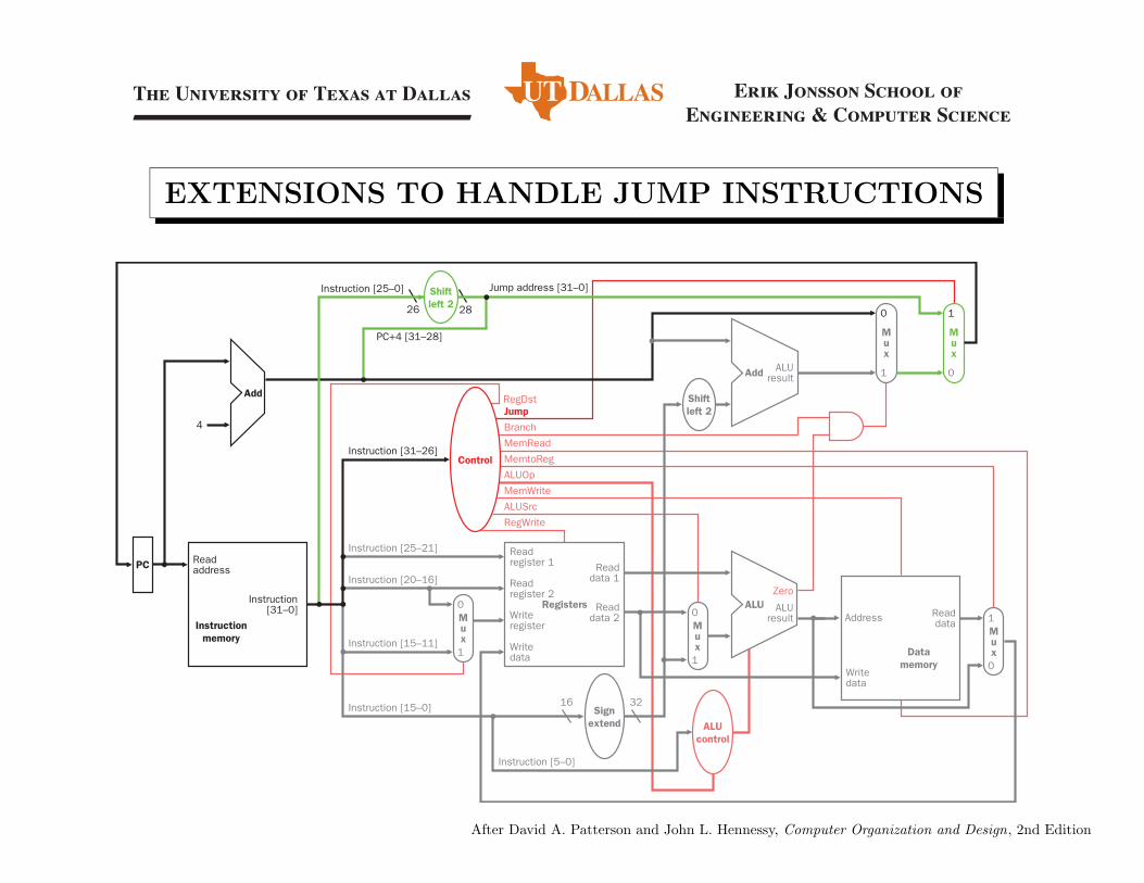
EXTENSIONS TO HANDLE JUMP INSTRUCTIONS
Shiftleft 2
PC
Instructionmemory
Readaddress
Instruction[31–0]
Datamemory
Readdata
Writedata
RegistersWriteregister
Writedata
Readdata 1
Readdata 2
Readregister 1
Readregister 2
Instruction [15–11]
Instruction [20–16]
Instruction [25–21]
Add
ALUresult
Zero
Instruction [5–0]
MemtoRegALUOpMemWrite
RegWrite
MemReadBranchJumpRegDst
ALUSrc
Instruction [31–26]
4
Mux
Instruction [25–0] Jump address [31–0]
PC+4 [31–28]
Signextend
16 32Instruction [15–0]
1
Mux
1
0
Mux
0
1
Mux
0
1
ALUcontrol
Control
Add ALUresult
Mux
0
1 0
ALU
Shiftleft 226 28
Address

The University of Texas at Dallas Erik Jonsson School ofEngineering & Computer Science
c� C. D. Cantrell (09/2010)
DETAILED INSTRUCTION FORMATS (3)
j label Jump
2 Target6 26
jal label Jump and Link
3 Target6 26
jr Rs Jump Register
0 Rs 0 86 5 16 5

The University of Texas at Dallas Erik Jonsson School ofEngineering & Computer Science
c� C. D. Cantrell (09/2010)
PERFORMANCE OF A SINGLE-CYCLE IMPLEMENTATION
• Our simple design implements control, ALU operations, loads/stores, andbranches in one large combinational logic block
• Good news: Our design assures that every instruction takes exactly oneclock period
. CPI = 1
• Bad news: The clock period can be no shorter than the time required forthe instruction with the longest delay
. The instruction with the most steps is likely to be the slowest, otherthings (such as number of memory accesses) being equal
. The lw instruction uses five functional units in series (instruction memory,register file, ALU, data memory, and then the register file again)
. Example: Assume that memory accesses and ALU operations take 200ps each, while register accesses take 100 ps each
�With these assumptions, lw takes 800 ps
The University of Texas at Dallas Erik Jonsson School ofEngineering & Computer Science
After David A. Patterson and John L. Hennessy, Computer Organization and Design, 2nd Edition
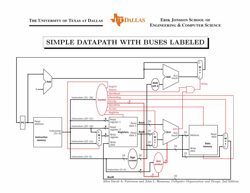
SIMPLE DATAPATH WITH BUSES LABELED
PC
Instructionmemory
Readaddress
Instruction[31–0]
Instruction [20 16]
Instruction [25 21]
Add
Instruction [5 0]
MemtoRegALUOpMemWrite
RegWrite
MemReadBranchRegDst
ALUSrc
Instruction [31 26]
4
16 32Instruction [15 0]
0
0Mux
0
1
Control
Add ALUresult
Mux
0
1
RegistersWriteregister
Writedata
Readdata 1
Readdata 2
Readregister 1
Readregister 2
Signextend
Mux1
ALUresult
Zero
PCSrc
Datamemory
Writedata
Readdata
Mux
1
Instruction [15 11]
ALUcontrol
Shiftleft 2
ALUAddress
2
3
2
6
5
5
532
32
32
32
32
32
32
BusW
BusA
BusB

©UCB, DAP 97
Worst Case Timing (Load)Clk
PC
Rs, Rt, Rd,Op, Func
Clk-to-Q
ALUctr
Instruction Memory Access Time
Old Value New Value
RegWr Old Value New Value
Delay through Control Logic
busARegister File Access Time
Old Value New Value
busBALU Delay
Old Value New Value
Old Value New Value
New ValueOld Value
ExtOp Old Value New Value
ALUSrc Old Value New Value
MemtoReg Old Value New Value
Address Old Value New Value
busW Old Value New
Delay through Extender & Mux
RegisterWrite Occurs
Data Memory Access Time

Multicycle Implementation: Concept
• Divide the data path into multiple clock cycles— instructions take from 3 to 5 cycles
ALU
Regs
Regs
DataMemory
Instr.Memory
IFInstruction
Fetch
RFRegister
Fetch
EXExecution
MEM.Memory
WBWriteback
PC
John L. Hennessy

The University of Texas at Dallas Erik Jonsson School ofEngineering & Computer Science
c� C. D. Cantrell (05/1999)
A MULTI-CYCLE IMPLEMENTATION (1)
• Each step in the execution of an instruction takes 1 clock period
. Di↵erent types of instructions can take di↵erent numbers of clock periods
� The clock period is no longer constrained by the longest execution time
. A functional unit can be used more than once per instruction if it is usedin di↵erent clock periods
� Less hardware may be needed than for a single-cycleimplementation
� Data and instruction memories can be combined into a single mainmemory
�We can get away with having a single ALU instead of an ALU and twoadders

The University of Texas at Dallas Erik Jonsson School ofEngineering & Computer Science
c� C. D. Cantrell (09/2011)
STEPS IN EXECUTING AN INSTRUCTION
Step R-type Memory reference Branches Jumps
Instruction IR = M[PC]Fetch PC = PC + 4
Instruction A = Reg[IR[25–21]]decode, B = Reg[IR[20–16]]
Register Fetch ALUOut = PC + (sign-extend(IR[15–0])<<2)Execution, ALUOut = A op B ALUOut = A If A == B then PC = PC[31–28]
address comp., + (sign-extend PC = ALUOut concatenated w/branch/jump (IR[15–0]) (IR[25–0]<<2)completion
Memory access Reg[IR[15–11]] Load: MDRor = ALUOut = M[ALUOut]
R-type completion Store: M[ALUOut] = BMemory read Load: Reg[IR[20–16]]completion = MDR

The University of Texas at Dallas Erik Jonsson School ofEngineering & Computer Science
c� C. D. Cantrell (05/1999)
TIMING ISSUES IN MULTCYCLE IMPLEMENTATIONS
• Edge-triggered timing
. Instructions may take multiple clock periods to complete execution
. An instruction may need to write to di↵erent functional units in di↵erentclock periods
• Data used in a clock period must be stabilized in one of two ways:
. Driven from a register that was written in an earlier clock period
. Driven from a combinational logic block with register-driven inputs
� Example: Suppose that the inputs to the ALU are stable
� The outputs are determined by the ALU’s combinational logic
� Therefore the ALU outputs really do not need to be latched
� If a functional unit is used more than once per instruction, then itsoutputs must be latched so that they will not be overwritten
� Not latching a functional unit’s outputs creates a multicycle delay path

A Multiple Cycle Delay Path• There is no register to save the results between:
— Register Fetch: busA Reg[rs]; busB Reg[rt]
— R-type Execution: ALU output busA op busB
— R-type Completion: Reg[rd] ALU output
Registers here to save outputs
of Rfetch?Register
here to save output of RExec?
ALU
3232
ALUControl
Instr. Reg
32Reg File
Ra
RwbusW
Rb5
532
busA
32busB
Rs
Rt
Mux
0
1
Rt
Rd
Mux 01
Mux
0
1 32
0
123
4
Zero
PCWrALUselA
ALUselB ALUOp
John L. Hennessy
The University of Texas at Dallas Erik Jonsson School ofEngineering & Computer Science
c� C. D. Cantrell (09/2011)
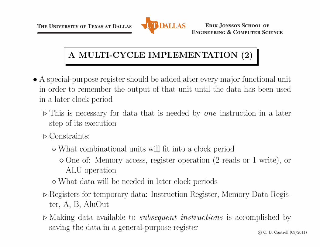
A MULTI-CYCLE IMPLEMENTATION (2)
• A special-purpose register should be added after every major functional unitin order to remember the output of that unit until the data has been usedin a later clock period
. This is necessary for data that is needed by one instruction in a laterstep of its execution
. Constraints:
�What combinational units will fit into a clock period
⇧ One of: Memory access, register operation (2 reads or 1 write), orALU operation
�What data will be needed in later clock periods
. Registers for temporary data: Instruction Register, Memory Data Regis-ter, A, B, AluOut
. Making data available to subsequent instructions is accomplished bysaving the data in a general-purpose register

The University of Texas at Dallas Erik Jonsson School ofEngineering & Computer Science
After David A. Patterson and John L. Hennessy, Computer Organization and Design, 2nd Edition
REGISTERS FOR TEMPORARY DATA
PC
Memory
Address
Instructionor data
Data
Instructionregister
RegistersRegister #
Data
Register #
Register #
ALU
Memorydata
register
A
B
ALUOut

The University of Texas at Dallas Erik Jonsson School ofEngineering & Computer Science
After David A. Patterson and John L. Hennessy, Computer Organization and Design, 2nd Edition
MULTICYCLE DATAPATH (FIRST CUT)
Shiftleft 2
PC
Memory
MemData
Writedata
Mux
0
1
RegistersWriteregister
Writedata
Readdata 1
Readdata 2
Readregister 1
Readregister 2
Mux
0
1
Mux
0
1
4
Instruction[15–0]
Signextend
3216
Instruction[25–21]
Instruction[20–16]
Instruction[15–0]
Instructionregister
1 Mux
0
32
Mux
ALUresult
ALUZero
Memorydata
register
Instruction[15–11]
A
B
ALUOut
0
1
Address

The University of Texas at Dallas Erik Jonsson School ofEngineering & Computer Science
After David A. Patterson and John L. Hennessy, Computer Organization and Design, 2nd Edition
MULTICYCLE DATAPATH AND CONTROL (FIRST CUT)
Shiftleft 2
MemtoReg
IorD MemRead MemWrite
PC
Memory
MemData
Writedata
Mux
0
1
RegistersWriteregister
Writedata
Readdata 1
Readdata 2
Readregister 1
Readregister 2
Instruction[15–11]
Mux
0
1
Mux
0
1
4
ALUOpALUSrcB
RegDst RegWrite
Instruction[15–0]
Instruction [5–0]
Signextend
3216
Instruction[25–21]
Instruction[20–16]
Instruction[15–0]
Instructionregister
1 Mux
0
32
ALUcontrol
Mux
0
1ALU
resultALU
ALUSrcA
ZeroA
B
ALUOut
IRWrite
Address
Memorydata
register

The University of Texas at Dallas Erik Jonsson School ofEngineering & Computer Science
After David A. Patterson and John L. Hennessy, Computer Organization and Design, 2nd Edition
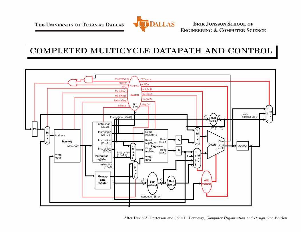
COMPLETED MULTICYCLE DATAPATH AND CONTROL
Shiftleft 2
PCMux
0
1
RegistersWriteregister
Writedata
Readdata 1
Readdata 2
Readregister 1
Readregister 2
Instruction[15–11]
Mux
0
1
Mux
0
1
4
Instruction[15–0]
Signextend
3216
Instruction[25–21]
Instruction[20–16]
Instruction[15–0]
Instructionregister
ALUcontrol
ALUresult
ALUZero
Memorydata
register
A
B
IorD
MemRead
MemWrite
MemtoReg
PCWriteCond
PCWrite
IRWrite
ALUOp
ALUSrcB
ALUSrcA
RegDst
PCSource
RegWrite
Control
Outputs
Op[5–0]
Instruction[31-26]
Instruction [5–0]
Mux
0
2
Jumpaddress [31-0]Instruction [25–0] 26 28
Shiftleft 2
PC [31-28]
1
1 Mux
0
32
Mux
0
1ALUOut
Memory
MemData
Writedata
Address

The University of Texas at Dallas Erik Jonsson School ofEngineering & Computer Science
c� C. D. Cantrell (09/2011)
STEPS IN EXECUTING AN INSTRUCTION
Step R-type Memory reference Branches Jumps
Instruction IR = M[PC]Fetch PC = PC + 4
Instruction A = Reg[IR[25–21]]decode, B = Reg[IR[20–16]]
Register Fetch ALUOut = PC + [(sign-extend(IR[15–0])<<2)Execution, ALUOut = A op B ALUOut = A If A == B then PC = PC[31–28]
address comp., + (sign-extend PC = ALUOut concatenated w/branch/jump (IR[15–0]) (IR[25–0]<<2)completion
Memory access Reg[IR[15–11]] Load: MDRor = ALUOut = M[ALUOut]
R-type completion Store: M[ALUOut] = BMemory read Load: Reg[IR[20–16]]completion = MDR

The University of Texas at Dallas Erik Jonsson School ofEngineering & Computer Science
c� C. D. Cantrell (09/2010)
SIMPLE QUESTIONS ABOUT TIMING
• How many clock periods are required to execute this program segment?
lw $t2, 0($t3)lw $t3, 4($t3)beq $t2, $t3, Label # Assume branch not takenadd $t5, $t2, $t3sw $t5, 8($t3)
Label: ...
. What happens during clock period 8?
. In what clock period does the addition of $t2 and $t3 actually takeplace?
(Thanks to Rama Sangireddy for these questions)

The University of Texas at Dallas Erik Jonsson School ofEngineering & Computer Science
c� C. D. Cantrell (09/2011)
IMPLEMENTING MULTI-CYCLE CONTROL
• Multi-cycle control is much more complex than single-cycle control
. Single-cycle control: A finite state machine with only one state
� Control can be implemented with purely combinational logic
. Multi-cycle control requires state elements and state transitions
� Control must be implemented with complex sequential logic
• The values of the control signals depend on:
. The instruction that is being executed
. The step that is being performed
• We will use the information that we have to specify a finite state machine
. The FSM can be specified graphically, or
. Using microprogramming (derived from a state transition table)

The University of Texas at Dallas Erik Jonsson School ofEngineering & Computer Science
After David A. Patterson and John L. Hennessy, Computer Organization and Design, 2nd Edition
METHODS FOR DESIGNING MULTICYCLE CONTROL
Initialrepresentation
Finite statediagram
Microprogram
Sequencingcontrol
Explicit nextstate function
Microprogram counter+ dispatch ROMS
Logicrepresentation
Logicequations
Truthtables
Implementationtechnique
Programmablelogic array
Read onlymemory

The University of Texas at Dallas Erik Jonsson School ofEngineering & Computer Science
After David A. Patterson and John L. Hennessy, Computer Organization and Design, 2nd Edition
FINITE STATE MACHINE CONTROL (OVERVIEW)
Memory accessinstructions(4 states)
R-type instructions(2 states)
Branch instruction(1 state)
Jump instruction(1 state)
Instruction fetch/decode and register fetch(2 states)
Start

The University of Texas at Dallas Erik Jonsson School ofEngineering & Computer Science
After David A. Patterson and John L. Hennessy, Computer Organization and Design, 2nd Edition
INSTRUCTION FETCH/DECODE FSM
ALUSrcA = 0ALUSrcB = 11ALUOp = 00
MemReadALUSrcA = 0
IorD = 0IRWrite
ALUSrcB = 01ALUOp = 00
PCWritePCSource = 00
Instruction fetchInstruction decode/
Register fetch
(Op = 'LW') or (Op = 'SW') (Op = R-type)
(Op
= 'B
EQ')
(Op
= 'J
MP'
)
01
Start
Memory reference FSM R-type FSM Branch FSM Jump FSM

The University of Texas at Dallas Erik Jonsson School ofEngineering & Computer Science
After David A. Patterson and John L. Hennessy, Computer Organization and Design, 2nd Edition
MEMORY REFERENCE FSM
MemWriteIorD = 1
MemReadIorD = 1
ALUSrcA = 1ALUSrcB = 10ALUOp = 00
RegWriteMemtoReg = 1
RegDst = 0
Memory address computation
(Op = 'LW') or (Op = 'SW')
Memoryaccess
Write-back step
(Op = 'SW')
(Op
= 'L
W')
4
2
53
From state 1
To state 0
Memoryaccess

The University of Texas at Dallas Erik Jonsson School ofEngineering & Computer Science
After David A. Patterson and John L. Hennessy, Computer Organization and Design, 2nd Edition
R-TYPE FSM
ALUSrcA = 1ALUSrcB = 00ALUOp = 10
RegDst = 1RegWrite
MemtoReg = 0
Execution
R-type completion
6
7
(Op = R-type)From state 1
To state 0
The University of Texas at Dallas Erik Jonsson School ofEngineering & Computer Science
After David A. Patterson and John L. Hennessy, Computer Organization and Design, 2nd Edition
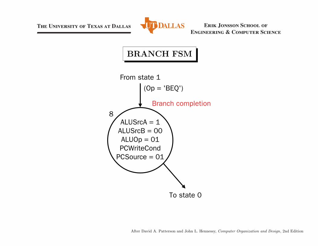
BRANCH FSM
Branch completion8
(Op = 'BEQ')From state 1
To state 0
ALUSrcA = 1ALUSrcB = 00ALUOp = 01PCWriteCond
PCSource = 01
The University of Texas at Dallas Erik Jonsson School ofEngineering & Computer Science
After David A. Patterson and John L. Hennessy, Computer Organization and Design, 2nd Edition
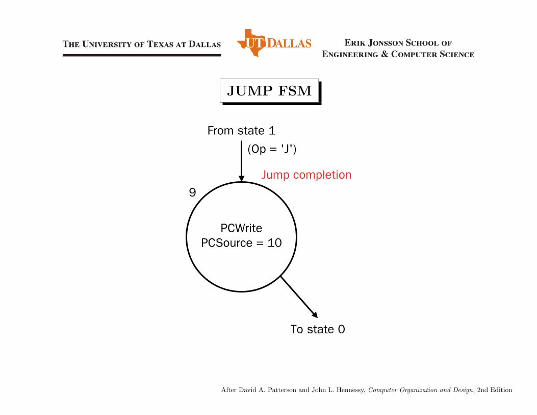
JUMP FSM
Jump completion9
(Op = 'J')From state 1
To state 0
PCWritePCSource = 10
The University of Texas at Dallas Erik Jonsson School ofEngineering & Computer Science
After David A. Patterson and John L. Hennessy, Computer Organization and Design, 2nd Edition
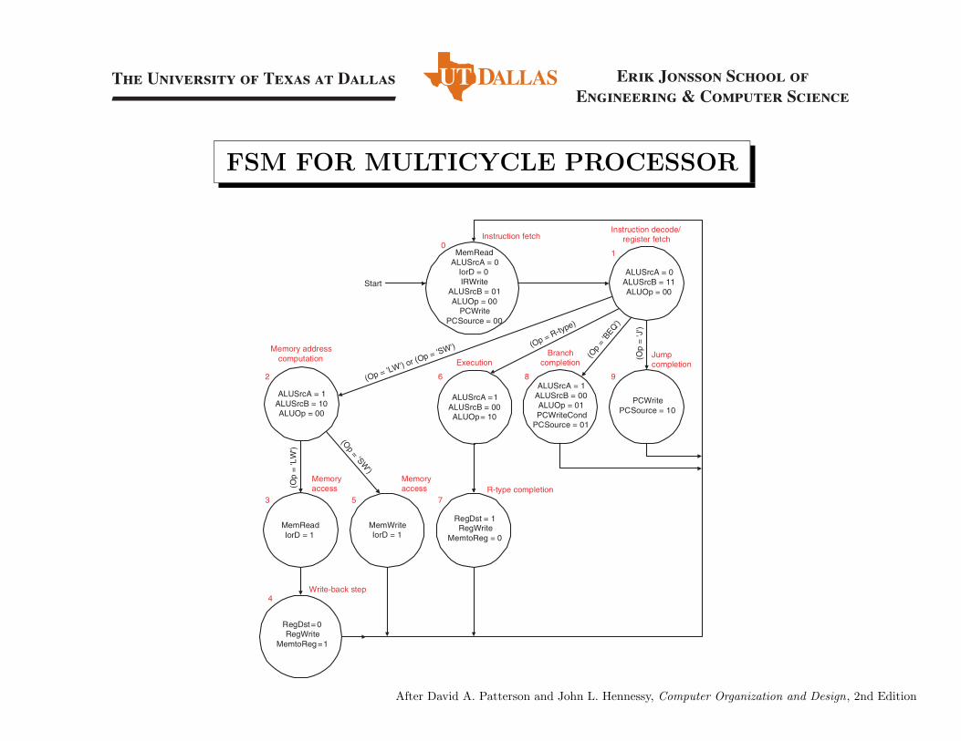
FSM FOR MULTICYCLE PROCESSOR
PCWritePCSource = 10
ALUSrcA = 1ALUSrcB = 00ALUOp = 01PCWriteCond
PCSource = 01
ALUSrcA =1ALUSrcB = 00ALUOp= 10
RegDst = 1RegWrite
MemtoReg = 0
MemWriteIorD = 1
MemReadIorD = 1
ALUSrcA = 1ALUSrcB = 10ALUOp = 00
RegDst = 0RegWrite
MemtoReg =1
ALUSrcA = 0ALUSrcB = 11ALUOp = 00
MemReadALUSrcA = 0
IorD = 0IRWrite
ALUSrcB = 01ALUOp = 00
PCWritePCSource = 00
Instruction fetchInstruction decode/
register fetch
Jumpcompletion
BranchcompletionExecution
Memory addresscomputation
Memoryaccess
Memoryaccess R-type completion
Write-back step
(Op = 'LW') or (Op = 'SW') (Op = R-type)
(Op
= 'B
EQ')
(Op
= 'J
')
(Op = 'SW')
(Op
= 'L
W')
4
01
9862
753
Start
The University of Texas at Dallas Erik Jonsson School ofEngineering & Computer Science
After David A. Patterson and John L. Hennessy, Computer Organization and Design, 2nd Edition
COMPLETED MULTICYCLE DATAPATH AND CONTROL
Shiftleft 2
PCMux
0
1
RegistersWriteregister
Writedata
Readdata 1
Readdata 2
Readregister 1
Readregister 2
Instruction[15–11]
Mux
0
1
Mux
0
1
4
Instruction[15–0]
Signextend
3216
Instruction[25–21]
Instruction[20–16]
Instruction[15–0]
Instructionregister
ALUcontrol
ALUresult
ALUZero
Memorydata
register
A
B
IorD
MemRead
MemWrite
MemtoReg
PCWriteCond
PCWrite
IRWrite
ALUOp
ALUSrcB
ALUSrcA
RegDst
PCSource
RegWrite
Control
Outputs
Op[5–0]
Instruction[31-26]
Instruction [5–0]
Mux
0
2
Jumpaddress [31-0]Instruction [25–0] 26 28
Shiftleft 2
PC [31-28]
1
1 Mux
0
32
Mux
0
1ALUOut
Memory
MemData
Writedata
Address

The University of Texas at Dallas Erik Jonsson School ofEngineering & Computer Science
c� C. D. Cantrell (09/2010)
CONTROL SIGNALS IN TERMS OF STATES
• Encoding:
. Need 4 bits (S0–S3) to encode 10 statess3 s2 s1 s0 s3 s2 s1 s0 s3 s2 s1 s0
0 0 0 0 1 0 0 0 0 0 1 1
10101001
dnoCetirWCP rof elbat hturT .betirWCP rof elbat hturT .a c. Truth table for IorD
s3 s2 s1 s0 s3 s2 s1 s0 s3 s2 s1 s0
0 0 0 0 0 1 0 1 0 0 0 0
0 0 1 1
d. Truth table for MemRead e. Truth table for MemWrite f. Truth table for IRWrite
s3 s2 s1 s0 s3 s2 s1 s0 s3 s2 s1 s0
0 1 0 0 1 0 0 1 1 0 0 0
g. Truth table for MemtoReg h. Truth table for PCSource1 i. Truth table for PCSource0
s3 s2 s1 s0 s3 s2 s1 s0 s3 s2 s1 s0
0 1 1 0 1 0 0 0 0 0 0 1
0 0 1 0
1BcrSULA rof elbat hturT .l0pOULA rof elbat hturT .k1pOULA rof elbat hturT .j
s3 s2 s1 s0 s3 s2 s1 s0 s3 s2 s1 s0
0 0 0 0 0 0 1 0 0 1 0 0
0 0 0 1 0 1 1 0 0 1 1 1
1 0 0 0
m. Truth table for ALUSrcB0 n. Truth table for ALUSrcA o. Truth table for RegWrite
s3 s2 s1 s0
0 1 1 1
p. Truth table for RegDst

The University of Texas at Dallas Erik Jonsson School ofEngineering & Computer Science
After David A. Patterson and John L. Hennessy, Computer Organization and Design, 4th Edition
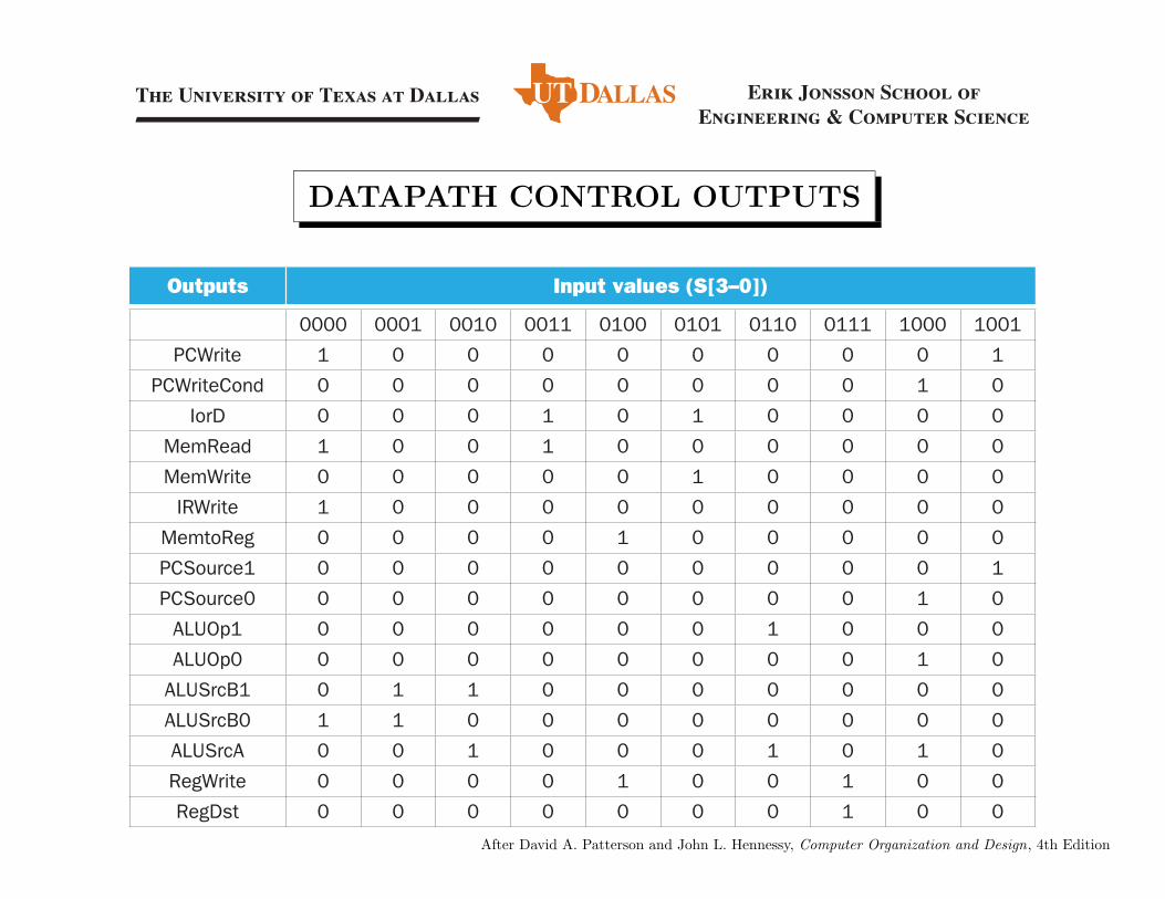
DATAPATH CONTROL TRUTH TABLE
)]0–3[S( seulav tupnIstuptuO
0000 0001 0010 0011 0100 0101 0110 0111 1000 1001PCWrite 1 0 0 0 0 0 0 0 0 1
PCWriteCond 0 0 0 0 0 0 0 0 1 0IorD 0 0 0 1 0 1 0 0 0 0
MemRead 1 0 0 1 0 0 0 0 0 0MemWrite 0 0 0 0 0 1 0 0 0 0
IRWrite 1 0 0 0 0 0 0 0 0 0MemtoReg 0 0 0 0 1 0 0 0 0 0PCSource1 0 0 0 0 0 0 0 0 0 1PCSource0 0 0 0 0 0 0 0 0 1 0
ALUOp1 0 0 0 0 0 0 1 0 0 0ALUOp0 0 0 0 0 0 0 0 0 1 0
ALUSrcB1 0 1 1 0 0 0 0 0 0 0ALUSrcB0 1 1 0 0 0 0 0 0 0 0ALUSrcA 0 0 1 0 0 0 1 0 1 0RegWrite 0 0 0 0 1 0 0 1 0 0RegDst 0 0 0 0 0 0 0 1 0 0

The University of Texas at Dallas Erik Jonsson School ofEngineering & Computer Science
c� C. D. Cantrell (09/2011)
NEXT-STATE FUNCTION
• Moore machine:
. The next state depends only on the present state
. Advantages:
�With edge-triggered updating of state elements (instruction registerand current state register), the next state outputs are clock-synchronized
� Speed (control outputs are stable early in the clock period)
� Footprint of the control unit
. Possible implementations of a next-state function:
� ROM, PLA, sequencer (leading to microprogrammed control)
• Mealy machine:
. The next state depends on both the present state and the inputs

The University of Texas at Dallas Erik Jonsson School ofEngineering & Computer Science
After David A. Patterson and John L. Hennessy, Computer Organization and Design, 4th Edition
IMPLEMENTATION OF THE NEXT-STATE FUNCTION
PCWritePCWriteCondIorD
MemtoRegPCSourceALUOpALUSrcBALUSrcARegWriteRegDst
NS3NS2NS1NS0
Op5
Op4
Op3
Op2
Op1
Op0
S3 S2 S1 S0
State register
IRWrite
MemReadMemWrite
Instruction registeropcode field
Outputs
Control logic(combinational)
Inputs

The University of Texas at Dallas Erik Jonsson School ofEngineering & Computer Science
c� C. D. Cantrell (09/2011)
EXAMPLE OF LOGIC EQUATIONS (1)
• Encoding:
. Need 4 bits (S0–S3) to encode 10 states
. The encoding for the state is just the state number in base two
• The NS0 bit is set whenever the next-state number is odd
• Logic equations for the odd-numbered next states:(e.g., if current state = 2 and the opcode is for lw, then next state = 3)
NextState1 = State0 = S3·S2·S1·S0
NextState3 = State2·(Op=lw) = S3·S2·S1·S0·Op5·Op4·Op3·Op2·Op1·Op0
NextState5 = State2·(Op=sw) = S3·S2·S1·S0·Op5·Op4·Op3·Op2·Op1·Op0
NextState7 = State6 = S3·S2·S1·S0
NextState9 = State1·(Op=jmp) = S3·S2·S1·S0·Op5·Op4·Op3·Op2·Op1·Op0

The University of Texas at Dallas Erik Jonsson School ofEngineering & Computer Science
c� C. D. Cantrell (09/2011)
EXAMPLE OF LOGIC EQUATIONS (2)
• Logic equations for the bit NS0:
NS0 = S3·S2·S1·S0
+ S3·S2·S1·S0·Op5·Op4·Op3·Op2·Op1·Op0
+ S3·S2·S1·S0·Op5·Op4·Op3·Op2·Op1·Op0
+ S3·S2·S1·S0
+ S3·S2·S1·S0·Op5·Op4·Op3·Op2·Op1·Op0
• Logic equations for the bit NS3 (set only in states 8 and 9):
NS3 = state1·(Op=beq) + state1·(Op=jmp)
= S3·S2·S1·S0·Op5·Op4·Op3·Op2·Op1·Op0
+ S3·S2·S1·S0·Op5·Op4·Op3·Op2·Op1·Op0

pOsetats tnerruCtuptuO
PCWrite state0 + state9PCWriteCond state8IorD state3 + state5MemRead state0 + state3MemWrite state5IRWrite state0MemtoReg state4PCSource1 state9PCSource0 state8ALUOp1 state6ALUOp0 state8ALUSrcB1 state1 +state2 ALUSrcB0 state0 + state1ALUSrcA state2 + state6 + state8RegWrite state4 + state7RegDst state7NextState0 state4 + state5 + state7 + state8 + state9NextState1 state0NextState2 state1 (Op = 'lw') + (Op = 'sw') NextState3 state2 (Op = 'lw')NextState4 state3NextState5 state2 (Op = 'sw') NextState6 state1 (Op = 'R-type')NextState7 state6NextState8 state1 (Op = 'beq')NextState9 state1 (Op = 'jmp')

Op5 Op4 Op3 Op2 Op1 Op0 S3 S2 S1 S0
0 0 0 0 1 0 0 0 0 10 0 0 1 0 0 0 0 0 1
a. The truth table for the NS3 output, active when the next state is 8 or 9. This signal is activated when the current state is 1.
Op5 Op4 Op3 Op2 Op1 Op0 S3 S2 S1 S0
0 0 0 0 0 0 0 0 0 11 0 1 0 1 1 0 0 1 0X X X X X X 0 0 1 1X X X X X X 0 1 1 0
b. The truth table for the NS2 output, which is active when the next state is 4, 5, 6, or 7. This situation occurs when the current state is one of 1, 2, 3, or 6.
Op5 Op4 Op3 Op2 Op1 Op0 S3 S2 S1 S0
0 0 0 0 0 0 0 0 0 11 0 0 0 1 1 0 0 0 11 0 1 0 1 1 0 0 0 11 0 0 0 1 1 0 0 1 0X X X X X X 0 1 1 0
c. The truth table for the NS1 output, which is active when the next state is 2, 3, 6, or 7. The next state is one of 2, 3, 6, or 7 only if the current state is one of 1, 2, or 6.
Op5 Op4 Op3 Op2 Op1 Op0 S3 S2 S1 S0
X X X X X X 0 0 0 01 0 0 0 1 1 0 0 1 01 0 1 0 1 1 0 0 1 0X X X X X X 0 1 1 00 0 0 0 1 0 0 0 0 1
d. The truth table for the NS0 output, which is active when the next state is 1, 3, 5, 7, or 9. This happens only if the current state is one of 0, 1, 2, or 6.

The University of Texas at Dallas Erik Jonsson School ofEngineering & Computer Science
c� C. D. Cantrell (09/2010)
ROM IMPLEMENTATION (1)
• Read-Only Memory (ROM)
. Values in memory locations are fixed when the ROM is manufactured
. A ROM can be used to implement a truth table
. The addresses are the 10-bit values of the inputs
� 6 opcode bits plus 4 state bits
� There are 210 = 1024 addresses for our instruction set
� S3–S0 are the low-order bits of the address
. Each memory location holds a 20-bit word
� 16 control bits plus 4 next-state bits
� NS3–NS0 are the low-order bits of the control word
. Can’t have don’t cares in an address ) lots of redundancy
. The size of a single-table ROM is 20⇥ 210 = 20 kb

The University of Texas at Dallas Erik Jonsson School ofEngineering & Computer Science
c� C. D. Cantrell (09/2010)
ROM IMPLEMENTATION (2)
• A two-table ROM can be much smaller than a single-table ROM
. One table uses S3–S0 (the low 4 bits of the address) to index the controlsignals
� This table provides the high 16 bits of the output
� The size of this table is 24 ⇥ 16 = 256 bits
. The second table uses S3–S0 and the opcode to determine NS3–NS0
� This table provides the low 4 bits of the output
� The size of this table is 210 ⇥ 4 = 4096 bits
. The outputs of the two tables are concatenated to obtain the full controlword
. The size of a two-table ROM is 256 + 4096 ⇡ 4.3 kb
The University of Texas at Dallas Erik Jonsson School ofEngineering & Computer Science
After David A. Patterson and John L. Hennessy, Computer Organization and Design, 4th Edition
DATAPATH CONTROL OUTPUTS
)]0–3[S( seulav tupnIstuptuO
0000 0001 0010 0011 0100 0101 0110 0111 1000 1001PCWrite 1 0 0 0 0 0 0 0 0 1
PCWriteCond 0 0 0 0 0 0 0 0 1 0IorD 0 0 0 1 0 1 0 0 0 0
MemRead 1 0 0 1 0 0 0 0 0 0MemWrite 0 0 0 0 0 1 0 0 0 0
IRWrite 1 0 0 0 0 0 0 0 0 0MemtoReg 0 0 0 0 1 0 0 0 0 0PCSource1 0 0 0 0 0 0 0 0 0 1PCSource0 0 0 0 0 0 0 0 0 1 0
ALUOp1 0 0 0 0 0 0 1 0 0 0ALUOp0 0 0 0 0 0 0 0 0 1 0
ALUSrcB1 0 1 1 0 0 0 0 0 0 0ALUSrcB0 1 1 0 0 0 0 0 0 0 0ALUSrcA 0 0 1 0 0 0 1 0 1 0RegWrite 0 0 0 0 1 0 0 1 0 0RegDst 0 0 0 0 0 0 0 1 0 0

The University of Texas at Dallas Erik Jonsson School ofEngineering & Computer Science
c� C. D. Cantrell (09/2011)
ROM IMPLEMENTATION (3)
• The following two tables show the entire contents of a two-table ROM
. The upper 16 bits of the control word depend only on the state inputs
. The lower 4 bits are NS3–NS0, which are determined by S3–S0 and theopcode
� An illegal opcode causes an Undefined Instruction exception
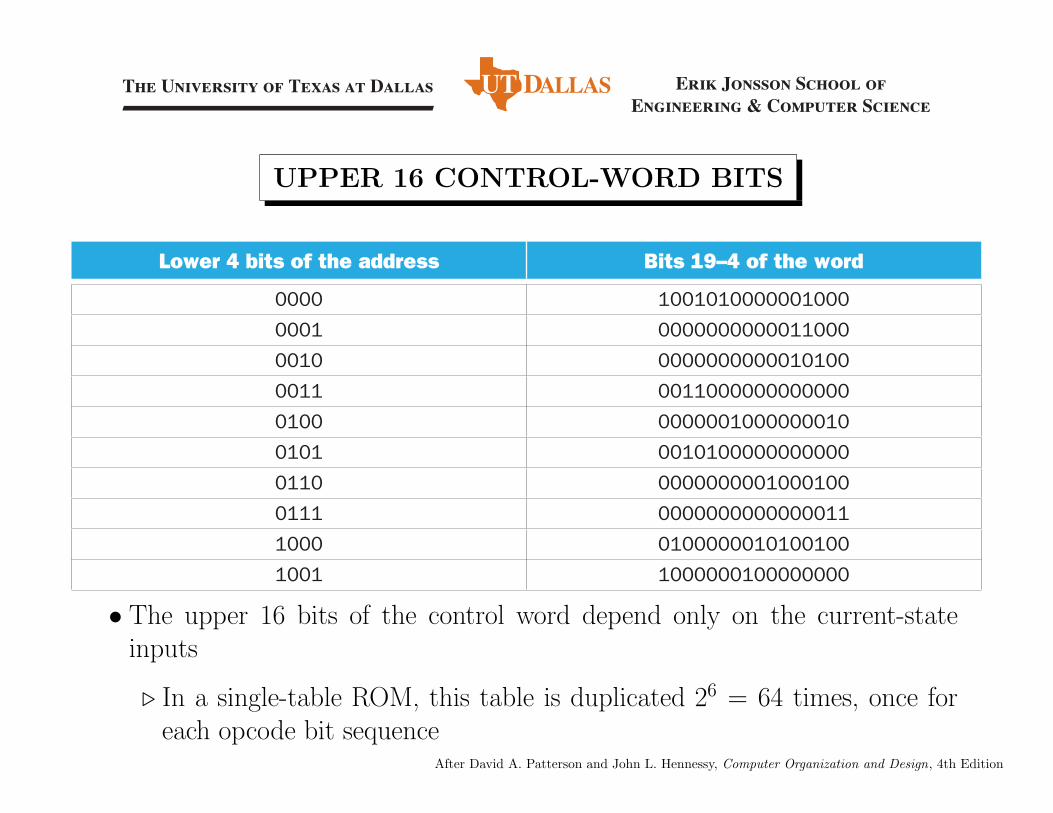
The University of Texas at Dallas Erik Jonsson School ofEngineering & Computer Science
After David A. Patterson and John L. Hennessy, Computer Organization and Design, 4th Edition
UPPER 16 CONTROL-WORD BITS
Lower 4 bits of the address Bits 19–4 of the word
00010000001010010000000110000000000010000010100000000000010000000000000011001100010000000100000000100000000000010100101000100010000000000110110000000000000011100010010100000010000100000000100000011001
• The upper 16 bits of the control word depend only on the current-stateinputs
. In a single-table ROM, this table is duplicated 26 = 64 times, once foreach opcode bit sequence
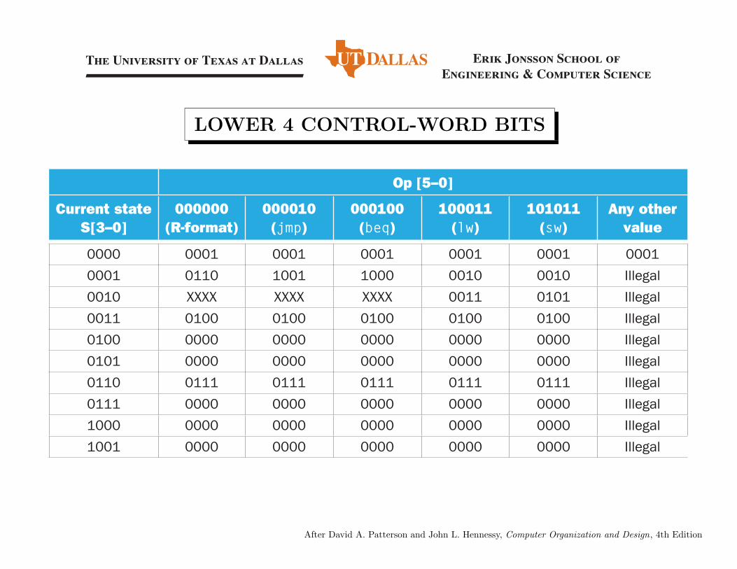
The University of Texas at Dallas Erik Jonsson School ofEngineering & Computer Science
After David A. Patterson and John L. Hennessy, Computer Organization and Design, 4th Edition
LOWER 4 CONTROL-WORD BITS
Op [5–0]
Current stateS[3–0]
000000(R-format)
000010(jmp)
000100(beq)
100011(lw)
101011(sw)
Any othervalue
0000 0001 0001 0001 0001 0001 00010001 0110 1001 1000 0010 0010 Illegal0010 XXXX XXXX XXXX 0011 0101 Illegal0011 0100 0100 0100 0100 0100 Illegal0100 0000 0000 0000 0000 0000 Illegal0101 0000 0000 0000 0000 0000 Illegal0110 0111 0111 0111 0111 0111 Illegal0111 0000 0000 0000 0000 0000 Illegal1000 0000 0000 0000 0000 0000 Illegal1001 0000 0000 0000 0000 0000 Illegal

The University of Texas at Dallas Erik Jonsson School ofEngineering & Computer Science
c� C. D. Cantrell (09/2011)
PLA IMPLEMENTATION (1)
• Programmed Logic Array (PLA) implementation of the combinational blockthat incorporates the next-state function
. Goal: Reduce the amount of control storage
. Cost: More complex decoding of the inputs
. Each AND term (minterm) = one line in a truth table
. Each NS bit is the sum (OR) of minterms
. Example: One of the two minterms in NS3 is
S3·S2·S1·S0·Op5·Op4·Op3·Op2·Op1·Op0
. In a standard PLA representation, each column in the input section rep-resents a minterm
. Each row in the output section represents a sum of minterms

The University of Texas at Dallas Erik Jonsson School ofEngineering & Computer Science
After David A. Patterson and John L. Hennessy, Computer Organization and Design, 4th Edition
PLA IMPLEMENTATION (2)
Op5
Op4
Op3
Op2
Op1
Op0
S3
S2
S1
S0
IorD
IRWrite
MemReadMemWrite
PCWritePCWriteCond
MemtoRegPCSource1
ALUOp1
ALUSrcB0ALUSrcARegWriteRegDstNS3NS2NS1NS0
ALUSrcB1ALUOp0
PCSource0

The University of Texas at Dallas Erik Jonsson School ofEngineering & Computer Science
c� C. D. Cantrell (09/2010)
SEQUENCER IMPLEMENTATION (1)
• For complex instructions, the next state is often the current state + 1
. A counter can increment the state number with an adder
. Must provide for branches when next state is not current state + 1
� Choose between incremented state and a di↵erent state
� The choice is based on the opcode and the current state
. Each control word must include control lines that determine how the nextstate is chosen
� Only need to provide a way to choose a non-sequential next state
� The control unit only needs to set NS3–NS0 when the next state is notsequential
� Can use external logic to do this e�ciently

Sequencer-based control unit
Opcode
State Reg
Inputs
Outputs
Control Logic MulticycleDatapathControls
1
Address Select Logic
Adder
Types of “branching” in our implementation:• Set state to 0• Dispatch (state 1 & 2)• Use incremented state number

The University of Texas at Dallas Erik Jonsson School ofEngineering & Computer Science
After David A. Patterson and John L. Hennessy, Computer Organization and Design, 4th Edition
SEQUENCER IMPLEMENTATION (2)
AddrCtl
Outputs
PLA or ROM
State
Address select logic
Op[5
–0]
Adder
Instruction registeropcode field
1
Control unit
Input
PCWritePCWriteCondIorD
MemtoRegPCSourceALUOpALUSrcBALUSrcARegWriteRegDst
IRWrite
MemReadMemWrite

The University of Texas at Dallas Erik Jonsson School ofEngineering & Computer Science
c� C. D. Cantrell (09/2010)
SEQUENCER IMPLEMENTATION (3)
• We have to provide for two types of branches
. In one type, we have to jump to selected states based on the opcode
� A common approach is to use dispatch ROMs
� An additional output, AddrCtl, indicates when a dispatch is needed
� There are two states in which the opcode determines the next state
� Can use two small dispatch ROMs
. A second type of branch: Go back to state 0 to start the next instruction
AddrCtl value Action
0 Set state to 01 Dispatch with ROM 12 Dispatch with ROM 23 Use the incremented state
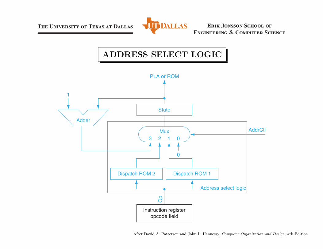
The University of Texas at Dallas Erik Jonsson School ofEngineering & Computer Science
After David A. Patterson and John L. Hennessy, Computer Organization and Design, 4th Edition
ADDRESS SELECT LOGIC
State
Op
Adder
1
PLA or ROM
Mux3 2 1 0
Dispatch ROM 1Dispatch ROM 2
0
AddrCtl
Address select logic
Instruction registeropcode field
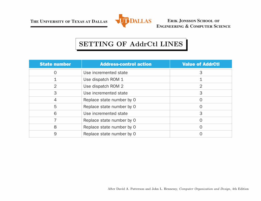
The University of Texas at Dallas Erik Jonsson School ofEngineering & Computer Science
After David A. Patterson and John L. Hennessy, Computer Organization and Design, 4th Edition
SETTING OF AddrCtl LINES
State number Address-control action Value of AddrCtl
3etats detnemercni esU011 MOR hctapsid esU122 MOR hctapsid esU23etats detnemercni esU300 yb rebmun etats ecalpeR400 yb rebmun etats ecalpeR53etats detnemercni esU600 yb rebmun etats ecalpeR700 yb rebmun etats ecalpeR800 yb rebmun etats ecalpeR9
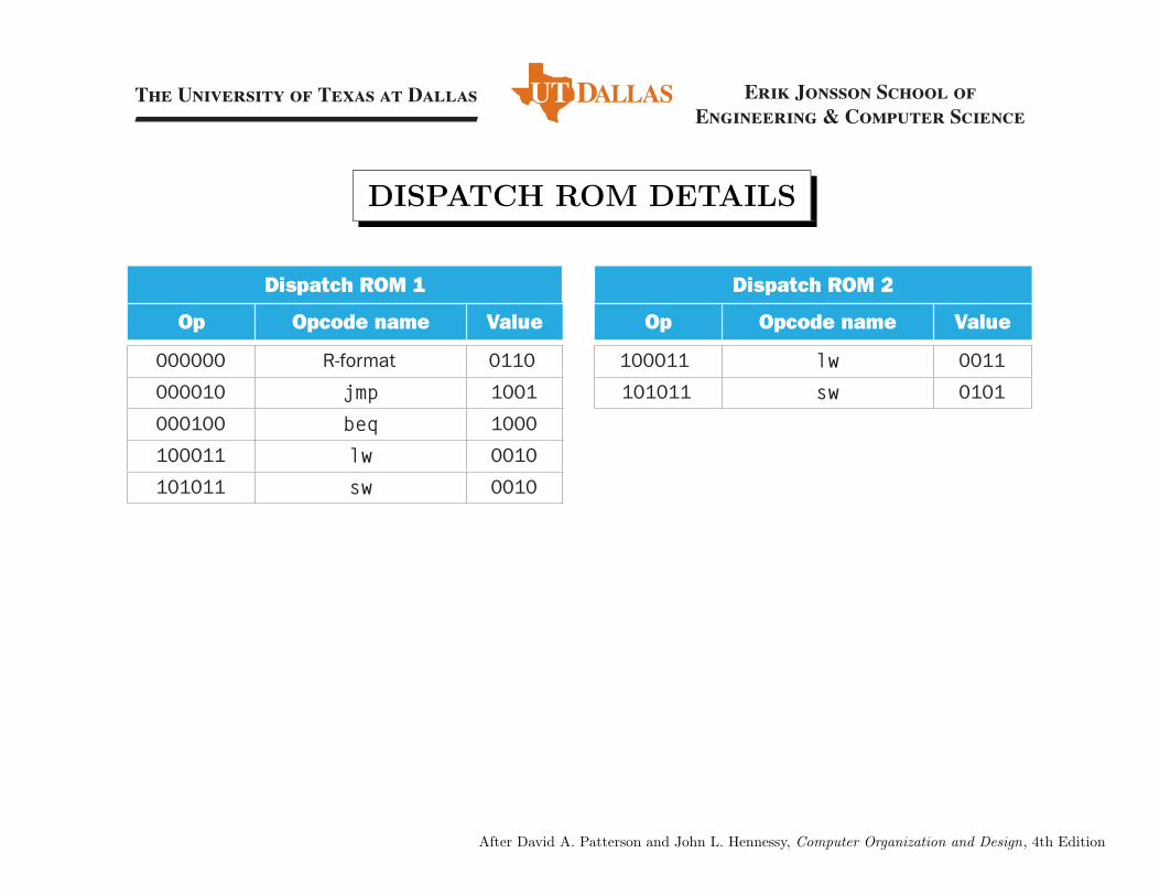
The University of Texas at Dallas Erik Jonsson School ofEngineering & Computer Science
After David A. Patterson and John L. Hennessy, Computer Organization and Design, 4th Edition
DISPATCH ROM DETAILS
2 MOR hctapsiD1 MOR hctapsiD
Op Opcode name Value Op Opcode name Value
000000 R-format 0110 100011 lw 0011000010 jmp 1001 101011 sw 0101000100 beq 1000100011 lw 0010101011 sw 0010

The University of Texas at Dallas Erik Jonsson School ofEngineering & Computer Science
After David A. Patterson and John L. Hennessy, Computer Organization and Design, 4th Edition
SEQUENCER CONTROL ROM CONTENTS
State number Control word bits 17–2 Control word bits 1–0
11000100000010100101000011000000000001
01001010000000000021100000000000011003000100000001000000400000000000001010051100100010000000006001100000000000000700001001010000001080000000000100000019
• The two LSBs are the value of AddrCtl
• The MSBs are identical to the MSBs in the smaller ROM in the the two-ROM implementation
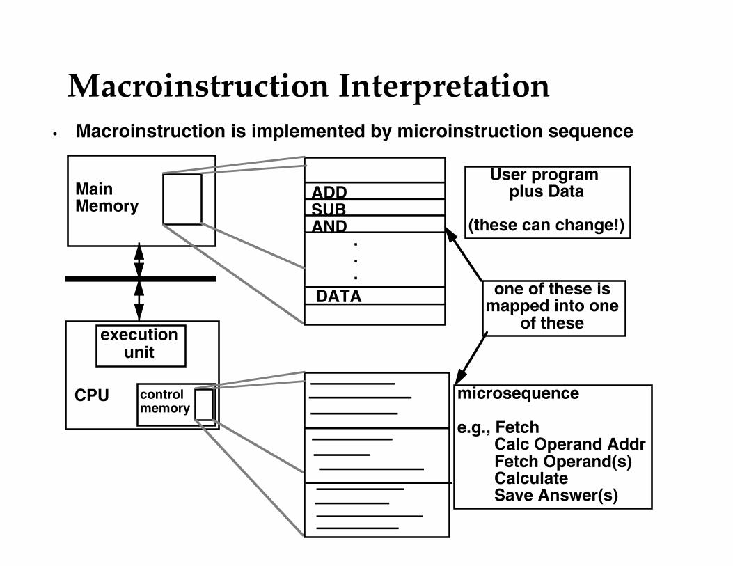
Macroinstruction Interpretation
MainMemory
executionunit
controlmemory
CPU
ADDSUBAND
DATA
.
.
.
User program plus Data
(these can change!)
microsequence
e.g., Fetch Calc Operand Addr Fetch Operand(s) Calculate Save Answer(s)
one of these ismapped into one
of these
• Macroinstruction is implemented by microinstruction sequence

The University of Texas at Dallas Erik Jonsson School ofEngineering & Computer Science
c� C. D. Cantrell (09/2010)
MICROPROGRAMMING (1)
• Microprogramming: Another specification methodology
. Useful if there are hundreds or thousands of opcodes, modes, cycles, etc.
. Signals are specified symbolically using microinstructions
. Strategy:
� Set of values of processor control signals = microinstruction
�Microinstruction sequence is determined by:
⇧ Inputs from MIPS instruction Opcode and Function fields⇧ Current state of the processor
. Would two implementations of the same ISA have the same microcode?
. What would a microassembler do?

The University of Texas at Dallas Erik Jonsson School ofEngineering & Computer Science
After David A. Patterson and John L. Hennessy, Computer Organization and Design, 4th Edition
MICROPROGRAMMING (2)
PCWritePCWriteCondIorD
MemtoRegPCSourceALUOpALUSrcBALUSrcARegWrite
AddrCtl
Outputs
Microcode memory
IRWrite
MemReadMemWrite
RegDst
Control unit
Input
Microprogram counter
Address select logic
Op[5
–0]
Adder
1
Instruction registeropcode field
BWrite
Datapath

The University of Texas at Dallas Erik Jonsson School ofEngineering & Computer Science
After David A. Patterson and John L. Hennessy, Computer Organization and Design, 4th Edition
MICROINSTRUCTION FORMAT
tnemmoCevitca slangiSeulaVeman dleiF
ALU control
Add ALUOp = 00 Cause the ALU to add.
Subt ALUOp = 01 Cause the ALU to subtract; this implements the compare for branches.
Func code ALUOp = 10 Use the instruction’s function code to determine ALU control.
SRC1PC ALUSrcA = 0 Use the PC as the fi rst ALU input.
A ALUSrcA = 1 Register A is the fi rst ALU input.
SRC2
B ALUSrcB = 00 Register B is the second ALU input.
4 ALUSrcB = 01 Use 4 as the second ALU input.
Extend ALUSrcB = 10 Use output of the sign extension unit as the second ALU input.
Extshft ALUSrcB = 11 Use the output of the shift-by-two unit as the second ALU input.
Register control
srebmun retsiger eht sa RI eht fo sdle fi tr dna sr eht gnisu sretsiger owt daeRdaeRand putting the data into registers A and B.
Write ALU RegWrite,RegDst = 1, MemtoReg = 0
Write a register using the rd fi eld of the IR as the register number and the contents of ALUOut as the data.
Write MDR RegWrite, RegDst = 0, MemtoReg = 1
Write a register using the rt fi eld of the IR as the register number and the contents of the MDR as the data.
Memory
Read PC MemRead, IorD = 0, IRWrite
Read memory using the PC as address; write result into IR (and the MDR).
Read ALU MemRead, IorD = 1
Read memory using ALUOut as address; write result into MDR.
Write ALU MemWrite, IorD = 1
Write memory using the ALUOut as address, contents of B as the data.
PC write control
ALU PCSource = 00, PCWrite
Write the output of the ALU into the PC.
ALUOut-cond PCSource = 01, PCWriteCond
If the Zero output of the ALU is active, write the PC with the contents of the register ALUOut.
Jump address PCSource = 10, PCWrite
Write the PC with the jump address from the instruction.
Sequencing
Seq AddrCtl = 11 Choose the next microinstruction sequentially.
Fetch AddrCtl = 00 Go to the fi rst microinstruction to begin a new instruction.
Dispatch 1 AddrCtl = 01 Dispatch using the ROM 1.
Dispatch 2 AddrCtl = 10 Dispatch using the ROM 2.

The University of Texas at Dallas Erik Jonsson School ofEngineering & Computer Science
After David A. Patterson and John L. Hennessy, Computer Organization and Design, 4th Edition
MICROCODE DISPATCH ROMs
2 elbat hctapsid edocorciM1 elbat hctapsid
Opcode fi eld Opcode name Value Opcode fi eld Opcode name Value
000000 R-format Rformat1 100011 lw LW2
000010 jmp JUMP1 101011 sw SW2
000100 beq BEQ1
100011 lw Mem1
101011 sw Mem1
The University of Texas at Dallas Erik Jonsson School ofEngineering & Computer Science
c� C. D. Cantrell (09/2010)
MAXIMAL vs. MINIMAL ENCODING
• No encoding
. 1 bit for each datapath operation
. Fast, requires lots of memory and logic
. The VAX 11/780 used 400 kb of memory
• Maximal encoding
. Send the microinstructions through logic to determine control signals
. Uses less memory but is slower
• Historical context of CISC:
. Too much logic to put on the processor die
. A separate ROM, PROM or NVRAM held the microcode
. Adding new instructions was easy
(Thanks to Rama Sangireddy)
Microprogramming Pros and Cons+ Flexibility
• Adapt to changes in organization, timing, technology• Can make changes late in design or in field
+ Can implement powerful instruction sets• Historical perspective: microprogramming contributed to
growth in ISA complexity and size+ Generality
• Can implement multiple ISAs on same machine.• Can tailor instruction set to application.
+ Compatibility• Many organizations, same instruction set
— Costly to implement— Slow
Bottom line: Very limited role in implementing modern ISAs in modern technologies.
Larger role for special-purpose machines.

Legacy Software & Microprogramming
• IBM bet company on 360 Instruction Set Architecture (ISA):— single instruction set for many classes of machines (8-
bit to 64-bit)• Stewart Tucker stuck with job of what to do about
software compatibility with earlier models— Why not use multiple microprograms to do multiple
instruction sets on the same microarchitecture?— Coined term “emulation”: instruction set interpreter in
microcode for non-native instruction set— Very successful: in early years of IBM 360 it was hard
to know whether old instruction set or new instruction set was more frequently used
The University of Texas at Dallas Erik Jonsson School ofEngineering & Computer Science
c� C. D. Cantrell (09/2010)
HISTORICAL PERSPECTIVE ON MICROPROGRAMMING
• Microprogramming was very important in the ’60s and ’70s
. Led to sophisticated ISAs and the VAX
• Pipelined RISC processors became popular in the ’80s
. Microinstructions can also be pipelined
• Implementations of the IA-32 architecture since the 80486 use:
. Hardwired control for simple instructions
� Execute in a few cycles
� FSM control implemented using PLA or “random” logic
. Microcoded control is used for more complex instructions
� Execute in many cycles; use central control store
• The IA-64 architecture uses a RISC-like ISA without a large control store
(Thanks to Rama Sangireddy)

VAX Microinstructions
USHF UALU USUB UJMP
11 063656895 87 84
001 = left010 = right . . .101 = left3
010 = A-B-1100 = A+B+1
00 = Nop01 = CALL10 = RTN
JumpAddress
SubroutineControl
ALUControl
ALU ShifterControl
• VAX Microarchitecture:— 96 bit control store— 30 fields— 4096 µinstructions for VAX ISA — encodes concurrently executable "micro-operations"

Microprogramming: One Inspiration for RISC
• If simple (micro) instructions can execute at high clock rate...• If you could write compilers to produce microinstructions…• If programs use mostly simple instructions and addressing
modes…• If microcode is kept in RAM instead of ROM so as to fix bugs
…• If same memory used for control memory could be used
instead as cache for “macroinstructions”…• Then why not skip instruction interpretation by a
microprogram and simply compile directly into lowest language of machine?— Together with inspiration coming from ISA bloat,
microprogramming help drove creation of ISAs that allowed simpler implementation, especially simpler control!

The University of Texas at Dallas Erik Jonsson School ofEngineering & Computer Science
c� C. D. Cantrell (09/2011)
EXCEPTION HANDLING (1)
• In the MIPS ISA, an exception is any unprogrammed change in controlflow
. The Cause register on coprocessor 0 holds a field that indicates thereason for the exception
. Externally caused: Interrupt (by, e.g., a signal from an I/O device)
. Internally caused, such as:
� Arithmetic overflow (Cause0 = 1)
� Undefined instruction (Cause0 = 0)
� There are other types: Floating-point exception, bus error, ...
. The exception program counter holds the address of the instructionthat caused the exception
. The status register holds an interrupt mask and a 3-deep stack for thekernel/user and interrupt enable bits

The University of Texas at Dallas Erik Jonsson School ofEngineering & Computer Science
After David A. Patterson and John L. Hennessy, Computer Organization and Design, 2nd Edition
EXCEPTION TYPES
Type of event From where? MIPS terminologyI/O device request External Interrupt
Invoke the O/S from user program Internal ExceptionArithmetic overflow Internal Exception
Undefined instruction Internal ExceptionHardware malfunction Either Exception
or Interrupt

MIPS R2000 CPU AND COPROCESSORS
CPU
Registers$0
$31
Arithmeticunit
Multiplydivide
Lo Hi
Coprocessor 1 (FPU)
Registers$0
$31
Arithmeticunit
Registers
BadVAddr
Coprocessor 0 (traps and memory)
StatusCauseEPC
Memory
PC

MIPS CP0 and Exception Handling Registers
TLBEntryHi
TLBEntryLo
TLB(TranslationLookaside
Buffer)
“Safe”Entries
IndexRegister
RandomRegister
ContextRegister
BadVAddrRegister
EPCRegister
PRIdRegister
StatusRegister
CauseRegister
Used with virtual memory
Used for exception processing

STATUS AND CAUSE REGISTERS
15 8 5 4 3 2 1 0
Interrupt
mask Old Previous Current
Kern
el/
user
Inte
rrupt
enable
Kern
el/
user
Kern
el/
user
Inte
rrupt
enable
Inte
rrupt
enable
MIPS R2000 STATUS REGISTER
15 10 5 2
Pendinginterrupts
Exceptioncode
MIPS R2000 CAUSE REGISTER
0
The University of Texas at Dallas Erik Jonsson School ofEngineering & Computer Science
c� C. D. Cantrell (09/2011)
EXCEPTION HANDLING (2)
• How control checks for the two exceptions that we implement:
. Undefined instruction
� Occurs when no next state numbered 2–9 is defined from state 1 bythe Opcode field of the instruction
� For this exception we add a next state, numbered 10, to the FSM
. Arithmetic overflow
�We use an asserted ALU Overflow signal to transition from state 7 toa new state, numbered 11
• Define a new control signal, IntCause, to set the LSB of the Cause register
• To handle these exceptions, we have to provide for the address of the exception-handling code, 0xC0000000, to be loaded into the PC

The University of Texas at Dallas Erik Jonsson School ofEngineering & Computer Science
After David A. Patterson and John L. Hennessy, Computer Organization and Design, 2nd Edition
MULTICYCLE DATA PATH WITH EXCEPTIONS
Shiftleft 2
Memory
MemData
Writedata
Mux
0
1
Instruction[15–11]
Mux
0
1
4
Instruction[15–0]
Signextend
3216
Instruction[25–21]
Instruction[20–16]
Instruction[15–0]
Instructionregister
ALUcontrol
ALUresult
ALUZero
Memorydata
register
A
B
IorD
MemRead
MemWrite
MemtoReg
PCWriteCond
PCWrite
IRWrite
Control
Outputs
Op[5–0]
Instruction[31-26]
Instruction [5–0]
Mux
0
2
Jumpaddress [31-0]Instruction [25–0] 26 28
Shiftleft 2
PC [31-28]
1
Address
EPC
CO 00 00 00 3
Cause
ALUOp
ALUSrcB
ALUSrcA
RegDst
PCSource
RegWrite
EPCWriteIntCauseCauseWrite
1
0
1 Mux
0
32
Mux
0
1
Mux
0
1
PC
Mux
0
1
RegistersWriteregister
Writedata
Readdata 1
Readdata 2
Readregister 1
Readregister 2
ALUOut

The University of Texas at Dallas Erik Jonsson School ofEngineering & Computer Science
After David A. Patterson and John L. Hennessy, Computer Organization and Design, 2nd Edition
STATES FOR EXCEPTION HANDLING
11
10
To state 0 to begin next instruction
PC Source = 11
ALUSrcA = 0ALUSrcB = 01ALUOp = 01
EPCWritePCWrite
IntCause = 0CauseWrite
ALUSrcA = 0ALUSrcB = 01ALUOp = 01
EPCWritePCWrite
PCSource = 11
IntCause = 1CauseWrite

The University of Texas at Dallas Erik Jonsson School ofEngineering & Computer Science
After David A. Patterson and John L. Hennessy, Computer Organization and Design, 2nd Edition
MULTICYCLE FSM WITH EXCEPTION HANDLING
ALUSrcA = 1ALUSrcB = 00ALUOp = 01PCWriteCond
PCSource = 01
ALUSrcA = 1ALUSrcB = 00ALUOp = 10
RegDst = 1RegWrite
MemtoReg = 0MemWriteIorD = 1
MemReadIorD = 1
ALUSrcA = 1ALUSrcB = 00ALUOp = 00
RegWriteMemtoReg = 1
RegDst = 0
ALUSrcA = 0ALUSrcB = 11ALUOp = 00
MemReadALUSrcA = 0
IorD = 0IRWrite
ALUSrcB = 01ALUOp = 00
PCWritePCSource = 00
Instruction fetchInstruction decode/
Register fetch
Jumpcompletion
BranchcompletionExecution
Memory addresscomputation
Memoryaccess
Memoryaccess R-type completion
Write-back step
(Op = 'LW') or (Op = 'SW') (Op = R-type)
(Op
= 'B
EQ')
(Op
= 'J
')
(Op = 'SW')
(Op
= 'L
W')
4
01
9862
7 11 1053
Start
(Op = other)
Overflow
Overflow
ALUSrcA = 0ALUSrcB = 01ALUOp = 01
EPCWritePCWrite
PCSource = 11
IntCause = 0CauseWrite
ALUSrcA = 0ALUSrcB = 01ALUOp = 01
EPCWritePCWrite
PCSource = 11
IntCause = 1CauseWrite
PCWritePCSource = 10