Embed Size (px)
Citation preview
1FEATURES
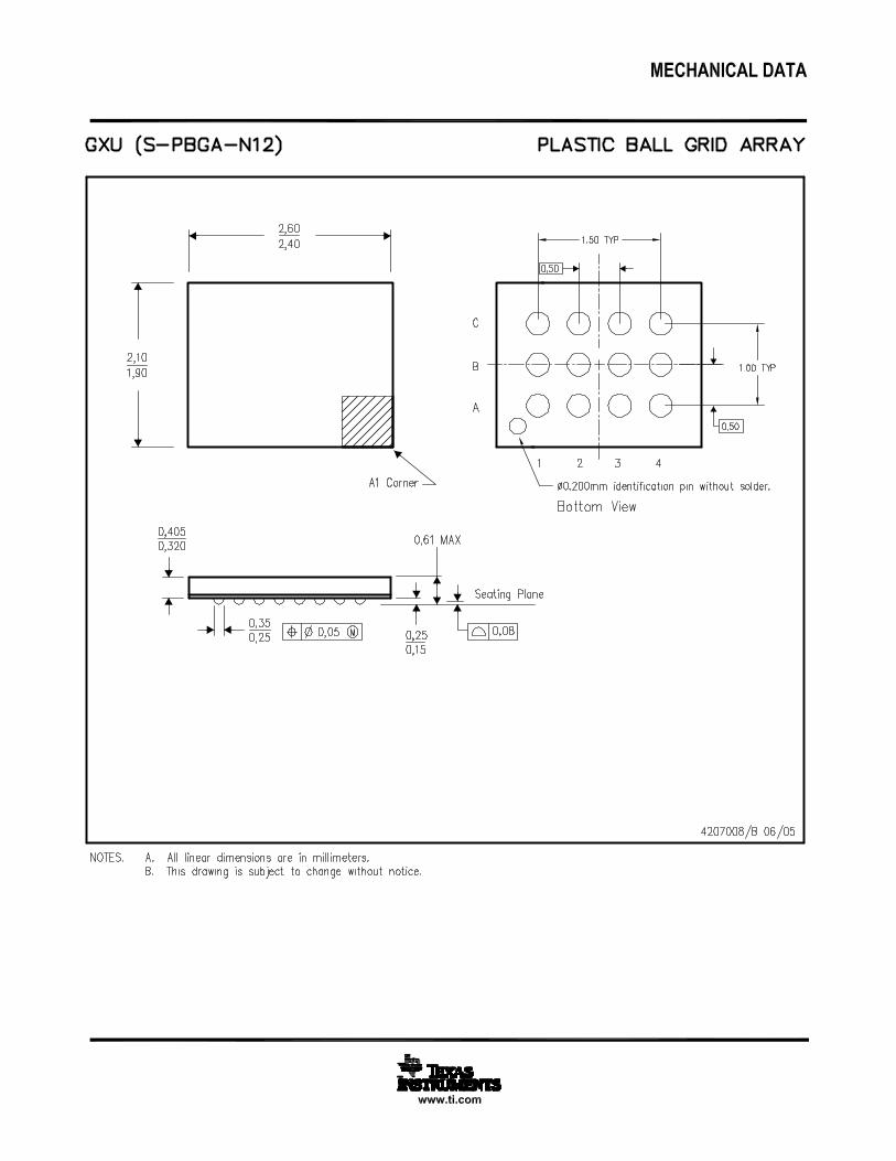
GXU/ZXU (BGA) PACKAGE
(TOP VIEW)
4
3
2
1
A B C
14
13
12
11
10
9
8
1
2
3
4
5
6
7 OE
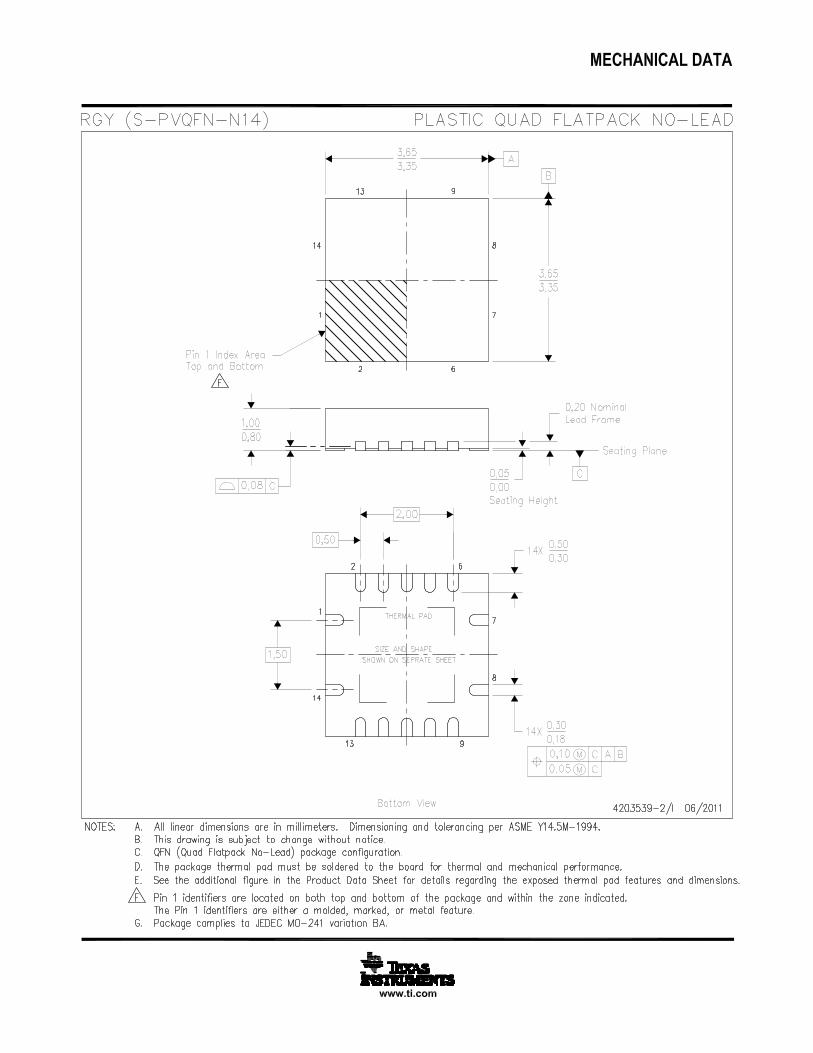
RGY PACKAGE(TOP VIEW)
1 14
7 8
2
3
4
5
6
13
12
11
10
9
B1B2B3B4NC
A1A2A3A4NC
OE
V
GN
D
CC
B
NC − No internal connection
D OR PW PACKAGE(TOP VIEW)
NC − No internal connection
GND
NC
A4
A3
A2
VCCA
NC
B4
B3
B2
B1
VCCB
A1
VC
CA
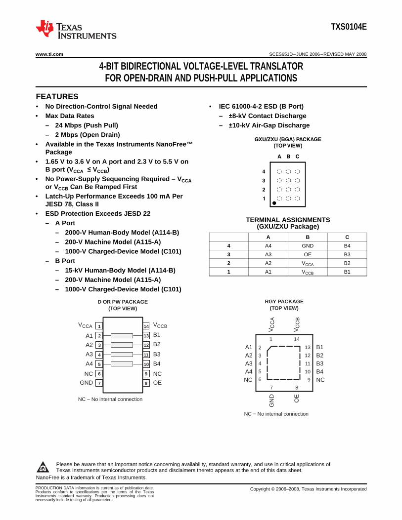
TXS0104E
www.ti.com............................................................................................................................................................... SCES651D–JUNE 2006–REVISED MAY 2008
4-BIT BIDIRECTIONAL VOLTAGE-LEVEL TRANSLATORFOR OPEN-DRAIN AND PUSH-PULL APPLICATIONS
2• No Direction-Control Signal Needed • IEC 61000-4-2 ESD (B Port)• Max Data Rates – ±8-kV Contact Discharge
– 24 Mbps (Push Pull) – ±10-kV Air-Gap Discharge– 2 Mbps (Open Drain)
• Available in the Texas Instruments NanoFree™Package
• 1.65 V to 3.6 V on A port and 2.3 V to 5.5 V onB port (VCCA ≤ VCCB)
• No Power-Supply Sequencing Required – VCCAor VCCB Can Be Ramped First
• Latch-Up Performance Exceeds 100 mA PerJESD 78, Class II
• ESD Protection Exceeds JESD 22TERMINAL ASSIGNMENTS– A Port (GXU/ZXU Package)
– 2000-V Human-Body Model (A114-B)A B C
– 200-V Machine Model (A115-A) 4 A4 GND B4– 1000-V Charged-Device Model (C101) 3 A3 OE B3
– B Port 2 A2 VCCA B2– 15-kV Human-Body Model (A114-B) 1 A1 VCCB B1– 200-V Machine Model (A115-A)– 1000-V Charged-Device Model (C101)
1
Please be aware that an important notice concerning availability, standard warranty, and use in critical applications ofTexas Instruments semiconductor products and disclaimers thereto appears at the end of this data sheet.
2NanoFree is a trademark of Texas Instruments.
PRODUCTION DATA information is current as of publication date. Copyright © 2006–2008, Texas Instruments IncorporatedProducts conform to specifications per the terms of the TexasInstruments standard warranty. Production processing does notnecessarily include testing of all parameters.

YZT (WCSP) PACKAGE
(TOP VIEW)
D
C
B
A
3 2 1
DESCRIPTION/ORDERING INFORMATION
TXS0104E
SCES651D–JUNE 2006–REVISED MAY 2008............................................................................................................................................................... www.ti.com
TERMINAL ASSIGNMENTS(YZT Package)3 2 1
D A4 GND B4C A3 OE B3B A2 VCCA B2A A1 VCCB B1
This 4-bit noninverting translator uses two separate configurable power-supply rails. The A port is designed totrack VCCA. VCCA accepts any supply voltage from 1.65 V to 3.6 V. VCCA must be less than or equal to VCCB. TheB port is designed to track VCCB. VCCB accepts any supply voltage from 2.3 V to 5.5 V. This allows for low-voltagebidirectional translation between any of the 1.8-V, 2.5-V, 3.3-V, and 5-V voltage nodes.
When the output-enable (OE) input is low, all outputs are placed in the high-impedance state.
The TXS0104E is designed so that the OE input circuit is supplied by VCCA.
To ensure the high-impedance state during power up or power down, OE should be tied to GND through apulldown resistor; the minimum value of the resistor is determined by the current-sourcing capability of the driver.
ORDERING INFORMATIONTA PACKAGE (1) (2) ORDERABLE PART NUMBER TOP-SIDE MARKING (3)
NanoFree — WCSP(DSBGA)0.23-mm Large Bump – YZT Reel of 3000 TXS0104EYZTR 2N7(Pb-free) 0.625-mm maxheight)UFBGA – GXU TXS0104EGXUR
Reel of 2500 YF04EUFBGA – ZXU (Pb-free) TXS0104EZXUR
TXS0104ERGYRQFN – RGY Reel of 1000 YF04E–40°C to 85°C TXS0104ERGYRG4
TXS0104EDTube of 50
TXS0104EDG4SOIC – D TXS0104E
TXS0104EDRReel of 2500
TXS0104EDRG4TXS0104EPWR
TSSOP – PW Reel of 2000 YF04ETXS0104EPWRG4
(1) For the most current package and ordering information, see the Package Option Addendum at the end of this document, or see the TIwebsite at www.ti.com.
(2) Package drawings, thermal data, and symbolization are available at www.ti.com/packaging.(3) YZT: The actual top-side marking has three preceding characters to denote year, month, and sequence code, and one following
character to designate the assembly/test site. Pin 1 identifier indicates solder-bump composition (1 = SnPb, • = Pb-free).
2 Submit Documentation Feedback Copyright © 2006–2008, Texas Instruments Incorporated
Product Folder Link(s): TXS0104E

Absolute Maximum Ratings (1)
TXS0104E
www.ti.com............................................................................................................................................................... SCES651D–JUNE 2006–REVISED MAY 2008
PIN DESCRIPTIONPIN NO. BALL NO.
NAME FUNCTIOND, PW, GXU/ZXU YZTOR RGY1 B2 B2 VCCA A-port supply voltage. 1.65 V ≤ VCCA ≤ 3.6 V and VCCA ≤ VCCB.2 A1 A3 A1 Input/output A1. Referenced to VCCA.3 A2 B3 A2 Input/output A2. Referenced to VCCA.4 A3 C3 A3 Input/output A3. Referenced to VCCA.5 A4 D3 A4 Input/output A4. Referenced to VCCA.6 – – NC No connection. Not internally connected.7 B4 D2 GND Ground
3-state output-mode enable. Pull OE low to place all outputs in 3-state8 B3 C2 OE mode. Referenced to VCCA.9 – – NC No connection. Not internally connected.
10 C4 D1 B4 Input/output B4. Referenced to VCCB.11 C3 C1 B3 Input/output B3. Referenced to VCCB.12 C2 B1 B2 Input/output B2. Referenced to VCCB.13 C1 A1 B1 Input/output B1. Referenced to VCCB.14 B1 A2 VCCB B-port supply voltage. 2.3 V ≤ VCCB ≤ 5.5 V.
over operating free-air temperature range (unless otherwise noted)
MIN MAX UNITVCCA –0.5 4.6
Supply voltage range VVCCB –0.5 6.5
A port –0.5 4.6VI Input voltage range (2) V
B port –0.5 6.5A port –0.5 4.6Voltage range applied to any outputVO Vin the high-impedance or power-off state (2) B port –0.5 6.5A port –0.5 VCCA + 0.5
VO Voltage range applied to any output in the high or low state (2) (3) VB port –0.5 VCCB + 0.5
IIK Input clamp current VI < 0 –50 mAIOK Output clamp current VO < 0 –50 mAIO Continuous output current ±50 mA
Continuous current through each VCCA, VCCB, or GND ±100 mAD package (4) 86PW package (4) 113
θJA Package thermal impedance RGY package (5) 47 °C/WGXU/ZXU package (4) 128YZT package TBD
Tstg Storage temperature range –65 150 °C
(1) Stresses beyond those listed under "absolute maximum ratings" may cause permanent damage to the device. These are stress ratingsonly, and functional operation of the device at these or any other conditions beyond those indicated under "recommended operatingconditions" is not implied. Exposure to absolute-maximum-rated conditions for extended periods may affect device reliability.
(2) The input and output negative-voltage ratings may be exceeded if the input and output current ratings are observed.(3) The value of VCCA and VCCB are provided in the recommended operating conditions table.(4) The package thermal impedance is calculated in accordance with JESD 51-7.(5) The package thermal impedance is calculated in accordance with JESD 51-5.
Copyright © 2006–2008, Texas Instruments Incorporated Submit Documentation Feedback 3
Product Folder Link(s): TXS0104E
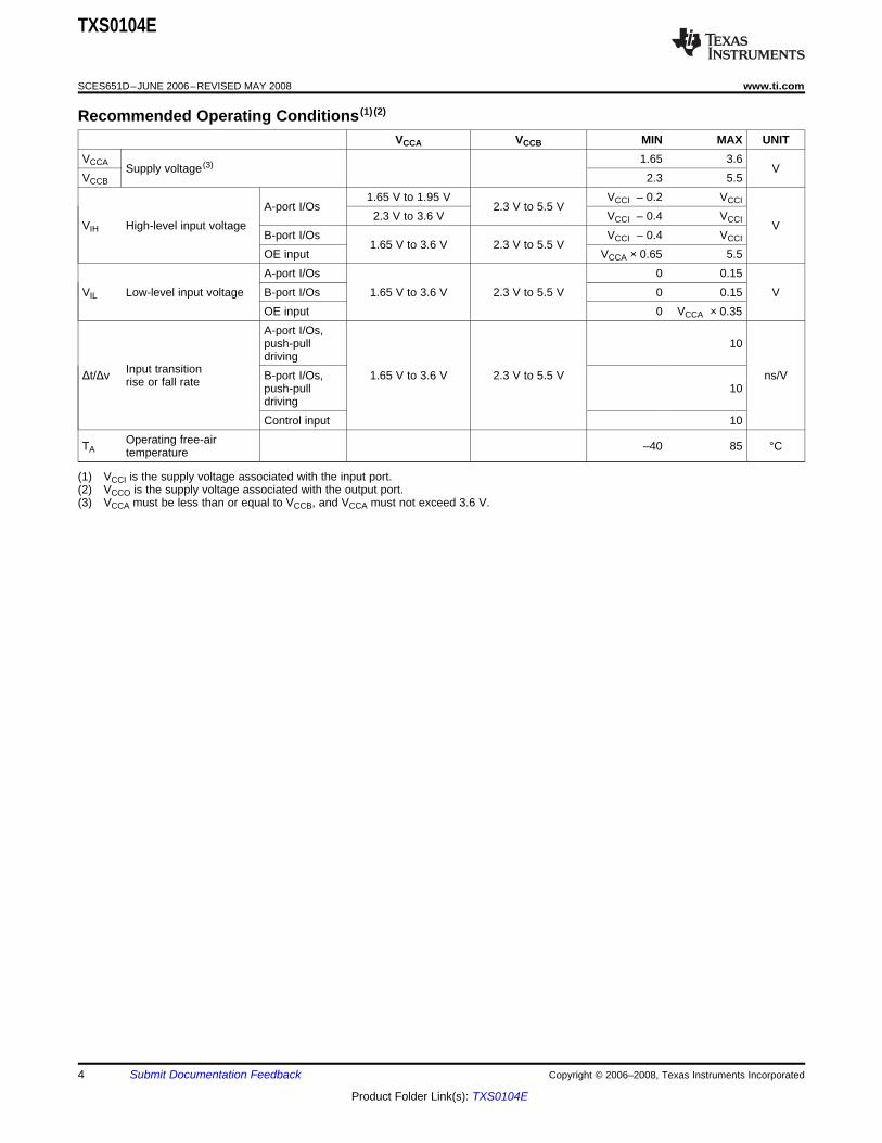
Recommended Operating Conditions (1) (2)
TXS0104E
SCES651D–JUNE 2006–REVISED MAY 2008............................................................................................................................................................... www.ti.com
VCCA VCCB MIN MAX UNITVCCA 1.65 3.6
Supply voltage (3) VVCCB 2.3 5.5
1.65 V to 1.95 V VCCI – 0.2 VCCIA-port I/Os 2.3 V to 5.5 V2.3 V to 3.6 V VCCI – 0.4 VCCIVIH High-level input voltage V
B-port I/Os VCCI – 0.4 VCCI1.65 V to 3.6 V 2.3 V to 5.5 VOE input VCCA × 0.65 5.5A-port I/Os 0 0.15
VIL Low-level input voltage B-port I/Os 1.65 V to 3.6 V 2.3 V to 5.5 V 0 0.15 VOE input 0 VCCA × 0.35A-port I/Os,push-pull 10driving
Input transitionΔt/Δv B-port I/Os, 1.65 V to 3.6 V 2.3 V to 5.5 V ns/Vrise or fall rate push-pull 10drivingControl input 10
Operating free-airTA –40 85 °Ctemperature
(1) VCCI is the supply voltage associated with the input port.(2) VCCO is the supply voltage associated with the output port.(3) VCCA must be less than or equal to VCCB, and VCCA must not exceed 3.6 V.
4 Submit Documentation Feedback Copyright © 2006–2008, Texas Instruments Incorporated
Product Folder Link(s): TXS0104E

Electrical Characteristics (1) (2) (3)
TXS0104E
www.ti.com............................................................................................................................................................... SCES651D–JUNE 2006–REVISED MAY 2008
over recommended operating free-air temperature range (unless otherwise noted)
TA = 25°C TA = 25°C to 85°CPARAMETER TEST CONDITIONS VCCA VCCB UNIT
MIN TYP MAX MIN MAXIOH = –20 µA,VOHA 1.65 V to 3.6 V 2.3 V to 5.5 V VCCA × 0.8 VVIB ≥ VCCB – 0.4 VIOL = 1 mA,VOLA 1.65 V to 3.6 V 2.3 V to 5.5 V 0.4 VVIB ≤ 0.15 VIOH = –20 µA,VOHB 1.65 V to 3.6 V 2.3 V to 5.5 V VCCB × 0.8 VVIA ≥ VCCA – 0.2 VIOL = 1 mA,VOLB 1.65 V to 3.6 V 2.3 V to 5.5 V 0.4 VVIA ≤ 0.15 V
II OE VI = VCCI or GND 1.65 V to 3.6 V 2.3 V to 5.5 V ±1 ±2 µAIOZ A or B port OE = VIL 1.65 V to 3.6 V 2.3 V to 5.5 V ±1 ±2 µA
1.65 V to VCCB 2.3 V to 5.5 V 2.4VI = VO = Open,ICCA 3.6 V 0 2.2 µAIO = 0
0 5.5 V –11.65 V to VCCB 2.3 V to 5.5 V 12
VI = VO = Open,ICCB 3.6 V 0 –1 µAIO = 00 5.5 V 1
VI = VO = Open,ICCA + ICCB 1.65 V to VCCB 2.3 V to 5.5 V 14.4 µAIO = 0CI OE 3.3 V 3.3 V 2.5 3.5 pF
A port 5 6.5Cio 3.3 V 3.3 V pF
B port 12 16.5
(1) VCCI is the supply voltage associated with the input port.(2) VCCO is the supply voltage associated with the output port.(3) VCCA must be less than or equal to VCCB, and VCCA must not exceed 3.6 V.
Copyright © 2006–2008, Texas Instruments Incorporated Submit Documentation Feedback 5
Product Folder Link(s): TXS0104E
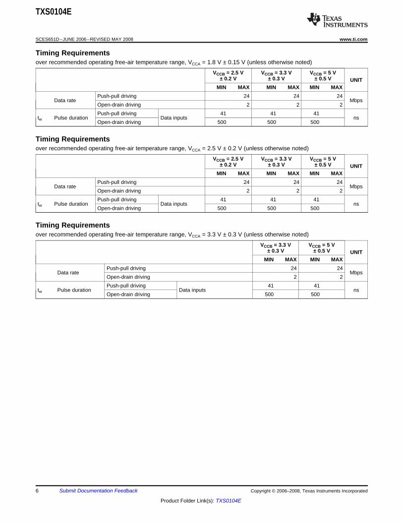
Timing Requirements
Timing Requirements
Timing Requirements
TXS0104E
SCES651D–JUNE 2006–REVISED MAY 2008............................................................................................................................................................... www.ti.com
over recommended operating free-air temperature range, VCCA = 1.8 V ± 0.15 V (unless otherwise noted)
VCCB = 2.5 V VCCB = 3.3 V VCCB = 5 V± 0.2 V ± 0.3 V ± 0.5 V UNIT
MIN MAX MIN MAX MIN MAXPush-pull driving 24 24 24
Data rate MbpsOpen-drain driving 2 2 2Push-pull driving 41 41 41
tw Pulse duration Data inputs nsOpen-drain driving 500 500 500
over recommended operating free-air temperature range, VCCA = 2.5 V ± 0.2 V (unless otherwise noted)
VCCB = 2.5 V VCCB = 3.3 V VCCB = 5 V± 0.2 V ± 0.3 V ± 0.5 V UNIT
MIN MAX MIN MAX MIN MAXPush-pull driving 24 24 24
Data rate MbpsOpen-drain driving 2 2 2Push-pull driving 41 41 41
tw Pulse duration Data inputs nsOpen-drain driving 500 500 500
over recommended operating free-air temperature range, VCCA = 3.3 V ± 0.3 V (unless otherwise noted)
VCCB = 3.3 V VCCB = 5 V± 0.3 V ± 0.5 V UNIT
MIN MAX MIN MAXPush-pull driving 24 24
Data rate MbpsOpen-drain driving 2 2Push-pull driving 41 41
tw Pulse duration Data inputs nsOpen-drain driving 500 500
6 Submit Documentation Feedback Copyright © 2006–2008, Texas Instruments Incorporated
Product Folder Link(s): TXS0104E

Switching Characteristics
TXS0104E
www.ti.com............................................................................................................................................................... SCES651D–JUNE 2006–REVISED MAY 2008
over recommended operating free-air temperature range, VCCA = 1.8 V ± 0.15 V (unless otherwise noted)
VCCB = 2.5 V VCCB = 3.3 V VCCB = 5 VFROM TO TEST ± 0.2 V ± 0.3 V ± 0.5 VPARAMETER UNIT(INPUT) (OUTPUT) CONDITIONS
MIN MAX MIN MAX MIN MAXPush-pull driving 4.6 4.7 5.8
tPHL Open-drain driving 2.9 8.8 2.9 9.6 3 10A B ns
Push-pull driving 6.8 6.8 7tPLH Open-drain driving 45 260 36 208 27 198
Push-pull driving 4.4 4.5 4.7tPHL Open-drain driving 1.9 5.3 1.1 4.4 1.2 4
B A nsPush-pull driving 5.3 4.5 0.5
tPLH Open-drain driving 45 175 36 140 27 102ten OE A or B 200 200 200 nstdis OE A or B 50 40 35 ns
Push-pull driving 3.2 9.5 2.3 9.3 2 7.6trA A-port rise time ns
Open-drain driving 38 165 30 132 22 95Push-pull driving 4 10.8 2.7 9.1 2.7 7.6
trB B-port rise time nsOpen-drain driving 34 145 23 106 10 58Push-pull driving 2 5.9 1.9 6 1.7 13.3
tfA A-port fall timeOpen-drain driving 4.4 6.9 4.3 6.4 4.2 6.1
nsPush-pull driving 2.9 7.6 2.8 7.5 2.8 8.8
tfB B-port fall timeOpen-drain driving 6.9 13.8 7.5 16.2 7 16.2
tSK(O) Channel-to-channel skew 1 1 1 nsPush-pull driving 24 24 24
Max data rate MbpsOpen-drain driving 2 2 2
Copyright © 2006–2008, Texas Instruments Incorporated Submit Documentation Feedback 7
Product Folder Link(s): TXS0104E

Switching Characteristics
TXS0104E
SCES651D–JUNE 2006–REVISED MAY 2008............................................................................................................................................................... www.ti.com
over recommended operating free-air temperature range, VCCA = 2.5 V ± 0.2 V (unless otherwise noted)
VCCB = 2.5 V VCCB = 3.3 V VCCB = 5 VFROM TO TEST ± 0.2 V ± 0.3 V ± 0.5 VPARAMETER UNIT(INPUT) (OUTPUT) CONDITIONS
MIN MAX MIN MAX MIN MAXPush-pull driving 3.2 3.3 3.4
tPHL Open-drain driving 1.7 6.3 2 6 2.1 5.8A B ns
Push-pull driving 3.5 4.1 4.4tPLH Open-drain driving 43 250 36 206 27 190
Push-pull driving 3 3.6 4.3tPHL Open-drain driving 1.8 4.7 2.6 4.2 1.2 4
B A nsPush-pull driving 2.5 1.6 0.7
tPLH Open-drain driving 44 170 37 140 27 103ten OE A or B 200 200 200 nstdis OE A or B 50 40 35 ns
Push-pull driving 2.8 7.4 2.6 6.6 1.8 5.6trA A-port rise time ns
Open-drain driving 34 149 28 121 24 89Push-pull driving 3.2 8.3 2.9 7.2 2.4 6.1
trB B-port rise time nsOpen-drain driving 35 151 24 112 12 64Push-pull driving 1.9 5.7 1.9 5.5 1.8 5.3
tfA A-port fall time nsOpen-drain driving 4.4 6.9 4.3 6.2 4.2 5.8Push-pull driving 2.2 7.8 2.4 6.7 2.6 6.6
tfB B-port fall time nsOpen-drain driving 5.1 8.8 5.4 9.4 5.4 10.4
tSK(O) Channel-to-channel skew 1 1 1 nsPush-pull driving 24 24 24
Max data rate MbpsOpen-drain driving 2 2 2
8 Submit Documentation Feedback Copyright © 2006–2008, Texas Instruments Incorporated
Product Folder Link(s): TXS0104E

Switching Characteristics
PRINCIPLES OF OPERATION
Applications
Architecture
TXS0104E
www.ti.com............................................................................................................................................................... SCES651D–JUNE 2006–REVISED MAY 2008
over recommended operating free-air temperature range, VCCA = 3.3 V ± 0.3 V (unless otherwise noted)
VCCB = 3.3 V VCCB = 5 VFROM TO TEST ± 0.3 V ± 0.5 VPARAMETER UNIT(INPUT) (OUTPUT) CONDITIONS
MIN MAX MIN MAXPush-pull driving 2.4 3.1
tPHL Open-drain driving 1.3 4.2 1.4 4.6A B ns
Push-pull driving 4.2 4.4tPLH Open-drain driving 36 204 28 165
Push-pull driving 2.5 3.3tPHL Open-drain driving 1 124 1 97
B A nsPush-pull driving 2.5 2.6
tPLH Open-drain driving 3 139 3 105ten OE A or B 200 200 nstdis OE A or B 40 35 ns
Push-pull driving 2.3 5.6 1.9 4.8trA A-port rise time ns
Open-drain driving 25 116 19 85Push-pull driving 2.5 6.4 2.1 7.4
trB B-port rise time nsOpen-drain driving 26 116 14 72Push-pull driving 2 5.4 1.9 5
tfA A-port fall time nsOpen-drain driving 4.3 6.1 4.2 5.7Push-pull driving 2.3 7.4 2.4 7.6
tfB B-port fall time nsOpen-drain driving 5 7.6 4.8 8.3
tSK(O) Channel-to-channel skew 1 1 nsPush-pull driving 24 24
Max data rate MbpsOpen-drain driving 2 2
The TXS0104E can be used in level-translation applications for interfacing devices or systems operating atdifferent interface voltages with one another. The TXS0104E is ideal for use in applications where an open-draindriver is connected to the data I/Os. The TXS0104E can also be used in applications where a push-pull driver isconnected to the data I/Os, but the TXB0104 might be a better option for such push-pull applications.
The TXS0104E architecture (see Figure 1) does not require a direction-control signal to control the direction ofdata flow from A to B or from B to A.
Copyright © 2006–2008, Texas Instruments Incorporated Submit Documentation Feedback 9
Product Folder Link(s): TXS0104E

VCCA
A
10 kΩ
B
T1 T2
VCCB
10 kΩ
One-shot One-shot
Gate Bias
Input Driver Requirements
Power Up
Enable and Disable
Pullup or Pulldown Resistors on I/O Lines
TXS0104E
SCES651D–JUNE 2006–REVISED MAY 2008............................................................................................................................................................... www.ti.com
Figure 1. Architecture of a TXS01xx Cell
Each A-port I/O has an internal 10-kΩ pullup resistor to VCCA, and each B-port I/O has an internal 10-kΩ pullupresistor to VCCB. The output one-shots detect rising edges on the A or B ports. During a rising edge, the one-shotturns on the PMOS transistors (T1,T2) for a short duration, which speeds up the low-to-high transition.
The fall time (tfA, tfB) of a signal depends on the output impedance of the external device driving the data I/Os ofthe TXS0104E. Similarly, the tPHL and max data rates also depend on the output impedance of the externaldriver. The values for tfA, tfB, tPHL, and maximum data rates in the data sheet assume that the output impedanceof the external driver is less than 50 Ω.
During operation, ensure that VCCA ≤ VCCB at all times. During power-up sequencing, VCCA ≥ VCCB does notdamage the device, so any power supply can be ramped up first.
The TXS0104E has an OE input that is used to disable the device by setting OE low, which places all I/Os in theHi-Z state. The disable time (tdis) indicates the delay between the time when OE goes low and when the outputsactually get disabled (Hi-Z). The enable time (ten) indicates the amount of time the user must allow for theone-shot circuitry to become operational after OE is taken high.
Each A-port I/O has an internal 10-kΩ pullup resistor to VCCA, and each B-port I/O has an internal 10-kΩ pullupresistor to VCCB. If a smaller value of pullup resistor is required, an external resistor must be added from the I/Oto VCCA or VCCB (in parallel with the internal 10-kΩ resistors).
10 Submit Documentation Feedback Copyright © 2006–2008, Texas Instruments Incorporated
Product Folder Link(s): TXS0104E

PARAMETER MEASUREMENT INFORMATION
VOH
VOL
From Output Under Test
LOAD CIRCUIT FOR ENABLE/DISABLETIME MEASUREMENT
S1
2 × VCCO
Open
50 k
tPLH tPHL
OutputControl
(low-levelenabling)
OutputWaveform 1
S1 at 2 × VCCO(see Note B)
OutputWaveform 2
S1 at GND(see Note B)
tPZL
tPZH
tPLZ
tPHZ
VCCA/2VCCA/2
VCCI
0 V
VCCO/2VOH
VOL
0 V
0.1 VCCO
VCCO/2
0.9 VCCOVCCO/2
0 V
VCCI
0 V
VCCI/2 VCCI/2
tw
Input
VCCA
VCCO
VOLTAGE WAVEFORMSPROPAGATION DELAY TIMES
VOLTAGE WAVEFORMSPULSE DURATION
VOLTAGE WAVEFORMSENABLE AND DISABLE TIMES
Output
Input
tPZL/tPLZtPHZ/tPZH
2 × VCCOOpen
TEST S1
A. CL includes probe and jig capacitance.B. Waveform 1 is for an output with internal conditions such that the output is low, except when disabled by the output control.
Waveform 2 is for an output with internal conditions such that the output is high, except when disabled by the output control.C. All input pulses are supplied by generators having the following characteristics: PRR10 MHz, ZO = 50 Ω, dv/dt ≥ 1 V/ns.D. The outputs are measured one at a time, with one transition per measurement.E. tPLZ and tPHZ are the same as tdis.F. tPZL and tPZH are the same as ten.G. tPLH and tPHL are the same as tpd.H. VCCI is the VCC associated with the input port.I. VCCO is the VCC associated with the output port.J. All parameters and waveforms are not applicable to all devices.
50 k
1 M15 pF
15 pF
DATA RATE, PULSE DURATION, PROPAGATION DELAY,OUTPUT RISE AND FALL TIME MEASUREMENT USING
A PUSH-PULL DRIVER
VCCOVCCI
DUT
IN OUT
1 M15 pF
DATA RATE, PULSE DURATION, PROPAGATION DELAY,OUTPUT RISE AND FALL TIME MEASUREMENT USING
AN OPEN-DRAIN DRIVER
VCCOVCCI
DUT
IN OUT
VCCI/2 VCCI/2
0.9 VCCOVCCO/2
tr
0.1 VCCO
tf
TXS0104E
www.ti.com............................................................................................................................................................... SCES651D–JUNE 2006–REVISED MAY 2008
Figure 2. Load Circuit and Voltage Waveforms
Copyright © 2006–2008, Texas Instruments Incorporated Submit Documentation Feedback 11
Product Folder Link(s): TXS0104E

PACKAGE OPTION ADDENDUM
www.ti.com 23-Oct-2010
Addendum-Page 1
PACKAGING INFORMATION
Orderable Device Status (1) Package Type PackageDrawing
Pins Package Qty Eco Plan (2) Lead/Ball Finish
MSL Peak Temp (3) Samples
(Requires Login)
TXS0104ED ACTIVE SOIC D 14 50 Green (RoHS& no Sb/Br)
CU NIPDAU Level-1-260C-UNLIM Contact TI Distributoror Sales Office
TXS0104EDG4 ACTIVE SOIC D 14 50 Green (RoHS& no Sb/Br)
CU NIPDAU Level-1-260C-UNLIM Contact TI Distributoror Sales Office
TXS0104EDR ACTIVE SOIC D 14 2500 Green (RoHS& no Sb/Br)
CU NIPDAU Level-1-260C-UNLIM Request Free Samples
TXS0104EDRG4 ACTIVE SOIC D 14 2500 Green (RoHS& no Sb/Br)
CU NIPDAU Level-1-260C-UNLIM Request Free Samples
TXS0104EGXUR ACTIVE BGAMICROSTAR
JUNIOR
GXU 12 2500 TBD SNPB Level-1-240C-UNLIM Purchase Samples
TXS0104EPWR ACTIVE TSSOP PW 14 2000 Green (RoHS& no Sb/Br)
CU NIPDAU Level-1-260C-UNLIM Request Free Samples
TXS0104EPWRG4 ACTIVE TSSOP PW 14 2000 Green (RoHS& no Sb/Br)
CU NIPDAU Level-1-260C-UNLIM Request Free Samples
TXS0104ERGYR ACTIVE VQFN RGY 14 3000 Green (RoHS& no Sb/Br)
CU NIPDAU Level-2-260C-1 YEAR Request Free Samples
TXS0104ERGYRG4 ACTIVE VQFN RGY 14 3000 Green (RoHS& no Sb/Br)
CU NIPDAU Level-2-260C-1 YEAR Request Free Samples
TXS0104EYZTR ACTIVE DSBGA YZT 12 3000 Green (RoHS& no Sb/Br)
SNAGCU Level-1-260C-UNLIM Request Free Samples
TXS0104EZXUR ACTIVE BGAMICROSTAR
JUNIOR
ZXU 12 2500 Green (RoHS& no Sb/Br)
SNAGCU Level-1-260C-UNLIM Request Free Samples
(1) The marketing status values are defined as follows:ACTIVE: Product device recommended for new designs.LIFEBUY: TI has announced that the device will be discontinued, and a lifetime-buy period is in effect.NRND: Not recommended for new designs. Device is in production to support existing customers, but TI does not recommend using this part in a new design.PREVIEW: Device has been announced but is not in production. Samples may or may not be available.OBSOLETE: TI has discontinued the production of the device.
(2) Eco Plan - The planned eco-friendly classification: Pb-Free (RoHS), Pb-Free (RoHS Exempt), or Green (RoHS & no Sb/Br) - please check http://www.ti.com/productcontent for the latest availabilityinformation and additional product content details.TBD: The Pb-Free/Green conversion plan has not been defined.
PACKAGE OPTION ADDENDUM
www.ti.com 23-Oct-2010
Addendum-Page 2
Pb-Free (RoHS): TI's terms "Lead-Free" or "Pb-Free" mean semiconductor products that are compatible with the current RoHS requirements for all 6 substances, including the requirement thatlead not exceed 0.1% by weight in homogeneous materials. Where designed to be soldered at high temperatures, TI Pb-Free products are suitable for use in specified lead-free processes.Pb-Free (RoHS Exempt): This component has a RoHS exemption for either 1) lead-based flip-chip solder bumps used between the die and package, or 2) lead-based die adhesive used betweenthe die and leadframe. The component is otherwise considered Pb-Free (RoHS compatible) as defined above.Green (RoHS & no Sb/Br): TI defines "Green" to mean Pb-Free (RoHS compatible), and free of Bromine (Br) and Antimony (Sb) based flame retardants (Br or Sb do not exceed 0.1% by weightin homogeneous material)
(3) MSL, Peak Temp. -- The Moisture Sensitivity Level rating according to the JEDEC industry standard classifications, and peak solder temperature.
Important Information and Disclaimer:The information provided on this page represents TI's knowledge and belief as of the date that it is provided. TI bases its knowledge and belief on informationprovided by third parties, and makes no representation or warranty as to the accuracy of such information. Efforts are underway to better integrate information from third parties. TI has taken andcontinues to take reasonable steps to provide representative and accurate information but may not have conducted destructive testing or chemical analysis on incoming materials and chemicals.TI and TI suppliers consider certain information to be proprietary, and thus CAS numbers and other limited information may not be available for release.
In no event shall TI's liability arising out of such information exceed the total purchase price of the TI part(s) at issue in this document sold by TI to Customer on an annual basis.
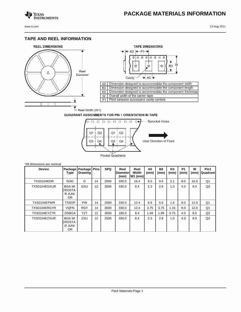
TAPE AND REEL INFORMATION
*All dimensions are nominal
Device PackageType
PackageDrawing
Pins SPQ ReelDiameter
(mm)
ReelWidth
W1 (mm)
A0(mm)
B0(mm)
K0(mm)
P1(mm)
W(mm)
Pin1Quadrant
TXS0104EDR SOIC D 14 2500 330.0 16.4 6.5 9.0 2.1 8.0 16.0 Q1
TXS0104EGXUR BGA MI CROSTA
R JUNI OR
GXU 12 2500 330.0 8.4 2.3 2.8 1.0 4.0 8.0 Q2
TXS0104EPWR TSSOP PW 14 2000 330.0 12.4 6.9 5.6 1.6 8.0 12.0 Q1
TXS0104ERGYR VQFN RGY 14 3000 330.0 12.4 3.75 3.75 1.15 8.0 12.0 Q1
TXS0104EYZTR DSBGA YZT 12 3000 180.0 8.4 1.49 1.99 0.75 4.0 8.0 Q2
TXS0104EZXUR BGA MI CROSTA
R JUNI OR
ZXU 12 2500 330.0 8.4 2.3 2.8 1.0 4.0 8.0 Q2
PACKAGE MATERIALS INFORMATION
www.ti.com 13-Aug-2011
Pack Materials-Page 1

*All dimensions are nominal
Device Package Type Package Drawing Pins SPQ Length (mm) Width (mm) Height (mm)
TXS0104EDR SOIC D 14 2500 346.0 346.0 33.0
TXS0104EGXUR BGA MICROSTARJUNIOR
GXU 12 2500 340.5 338.1 20.6
TXS0104EPWR TSSOP PW 14 2000 346.0 346.0 29.0
TXS0104ERGYR VQFN RGY 14 3000 346.0 346.0 29.0
TXS0104EYZTR DSBGA YZT 12 3000 210.0 185.0 35.0
TXS0104EZXUR BGA MICROSTARJUNIOR
ZXU 12 2500 340.5 338.1 20.6
PACKAGE MATERIALS INFORMATION
www.ti.com 13-Aug-2011
Pack Materials-Page 2


IMPORTANT NOTICE
Texas Instruments Incorporated and its subsidiaries (TI) reserve the right to make corrections, modifications, enhancements, improvements,and other changes to its products and services at any time and to discontinue any product or service without notice. Customers shouldobtain the latest relevant information before placing orders and should verify that such information is current and complete. All products aresold subject to TI’s terms and conditions of sale supplied at the time of order acknowledgment.
TI warrants performance of its hardware products to the specifications applicable at the time of sale in accordance with TI’s standardwarranty. Testing and other quality control techniques are used to the extent TI deems necessary to support this warranty. Except wheremandated by government requirements, testing of all parameters of each product is not necessarily performed.
TI assumes no liability for applications assistance or customer product design. Customers are responsible for their products andapplications using TI components. To minimize the risks associated with customer products and applications, customers should provideadequate design and operating safeguards.
TI does not warrant or represent that any license, either express or implied, is granted under any TI patent right, copyright, mask work right,or other TI intellectual property right relating to any combination, machine, or process in which TI products or services are used. Informationpublished by TI regarding third-party products or services does not constitute a license from TI to use such products or services or awarranty or endorsement thereof. Use of such information may require a license from a third party under the patents or other intellectualproperty of the third party, or a license from TI under the patents or other intellectual property of TI.
Reproduction of TI information in TI data books or data sheets is permissible only if reproduction is without alteration and is accompaniedby all associated warranties, conditions, limitations, and notices. Reproduction of this information with alteration is an unfair and deceptivebusiness practice. TI is not responsible or liable for such altered documentation. Information of third parties may be subject to additionalrestrictions.
Resale of TI products or services with statements different from or beyond the parameters stated by TI for that product or service voids allexpress and any implied warranties for the associated TI product or service and is an unfair and deceptive business practice. TI is notresponsible or liable for any such statements.
TI products are not authorized for use in safety-critical applications (such as life support) where a failure of the TI product would reasonablybe expected to cause severe personal injury or death, unless officers of the parties have executed an agreement specifically governingsuch use. Buyers represent that they have all necessary expertise in the safety and regulatory ramifications of their applications, andacknowledge and agree that they are solely responsible for all legal, regulatory and safety-related requirements concerning their productsand any use of TI products in such safety-critical applications, notwithstanding any applications-related information or support that may beprovided by TI. Further, Buyers must fully indemnify TI and its representatives against any damages arising out of the use of TI products insuch safety-critical applications.
TI products are neither designed nor intended for use in military/aerospace applications or environments unless the TI products arespecifically designated by TI as military-grade or "enhanced plastic." Only products designated by TI as military-grade meet militaryspecifications. Buyers acknowledge and agree that any such use of TI products which TI has not designated as military-grade is solely atthe Buyer's risk, and that they are solely responsible for compliance with all legal and regulatory requirements in connection with such use.
TI products are neither designed nor intended for use in automotive applications or environments unless the specific TI products aredesignated by TI as compliant with ISO/TS 16949 requirements. Buyers acknowledge and agree that, if they use any non-designatedproducts in automotive applications, TI will not be responsible for any failure to meet such requirements.
Following are URLs where you can obtain information on other Texas Instruments products and application solutions:
Products Applications
Audio www.ti.com/audio Communications and Telecom www.ti.com/communications
Amplifiers amplifier.ti.com Computers and Peripherals www.ti.com/computers
Data Converters dataconverter.ti.com Consumer Electronics www.ti.com/consumer-apps
DLP® Products www.dlp.com Energy and Lighting www.ti.com/energy
DSP dsp.ti.com Industrial www.ti.com/industrial
Clocks and Timers www.ti.com/clocks Medical www.ti.com/medical
Interface interface.ti.com Security www.ti.com/security
Logic logic.ti.com Space, Avionics and Defense www.ti.com/space-avionics-defense
Power Mgmt power.ti.com Transportation and www.ti.com/automotiveAutomotive
Microcontrollers microcontroller.ti.com Video and Imaging www.ti.com/video
RFID www.ti-rfid.com Wireless www.ti.com/wireless-apps
RF/IF and ZigBee® Solutions www.ti.com/lprf
TI E2E Community Home Page e2e.ti.com
Mailing Address: Texas Instruments, Post Office Box 655303, Dallas, Texas 75265Copyright © 2011, Texas Instruments Incorporated