Embed Size (px)
Citation preview

FEATURES HIGH BANDWIDTH: 80MHz
HIGH SLEW RATE: 55V/ µs
EXCELLENT VIDEO PERFORMANCE− 0.5dB GAIN FLATNESS: 25MHz− DIFFERENTIAL GAIN: 0.3%− DIFFERENTIAL PHASE: 0.7 ° INPUT RANGE INCLUDES GROUND
RAIL-TO-RAIL OUTPUT
SHUTDOWN CURRENT: < 5µA
LOW QUIESCENT CURRENT: 5.2mA
SINGLE-SUPPLY OPERATING RANGE:+2.7V to +3.3V
MicroSIZE PACKAGE: SC70-6
APPLICATIONS DIGITAL STILL CAMERAS
CAMERA PHONES
DIGITAL MEDIA PLAYERS
DIGITAL VIDEO CAMERAS
SET-TOP-BOX VIDEO FILTERS
OPTICAL POWER MONITORING
TRANSIMPEDANCE AMPLIFIERS
AUTOMATIC TEST EQUIPMENT
DESCRIPTIONThe high-speed OPA358 amplifier is optimized for 3Vsingle-supply operation. The output typically swings within5mV of GND with a 150Ω load connected to GND. Theinput common-mode range includes GND and swings towithin 1V of the positive power supply. The OPA358 offersexcellent video performance: 0.5dB gain flatness is25MHz, differential gain is 0.3%, and differential phase is0.7°.
The OPA358 is optimized for supply voltages from +2.7Vto +3.3V, with an operating range of +2.5V to +3.6V.Quiescent current is only 5.2mA per channel.
In shutdown mode, the quiescent current is reduced to< 5µA, dramatically reducing power consumption. This isespecially important in battery-operated equipment suchas digital still cameras (DSCs) or mobile phones withintegrated cameras.
The OPA358 is available in SC70-6, the smallest packagecurrently available for video applications.
OPA358 RELATED PRODUCTSFEATURES PRODUCT
G = 2, Internal Filter, Sag Correction, Shutdown, Video Amp OPA360
100MHz GBW, RR I/O, Shutdown, CMOS Amp OPA357
200MHz GBW, RR Out, Shutdown, CMOS Amp OPA355
38MHz GBW, RR I/O, CMOS Amp OPA350
> 200MHz, Shutdown, Video Buffer Amp, G = 2 OPA692
100MHz BW, Differential Input/Output, 3.3V Supply THS412x
All trademarks are the property of their respective owners.
Please be aware that an important notice concerning availability, standard warranty, and use in critical applications of Texas Instrumentssemiconductor products and disclaimers thereto appears at the end of this data sheet.
! !
OPA358
3V Single-Supply80MHz High-Speed Op Amp in SC70
SB0S296C − MARCH 2004 − REVISED FEBRUARY 2005
www.ti.com
Copyright 2004−2005, Texas Instruments Incorporated
"#$
SB0S296C − MARCH 2004 − REVISED FEBRUARY 2005
www.ti.com
2
PACKAGE/ORDERING INFORMATION (1)
PRODUCT PACKAGEPACKAGE
DESIGNATOR
SPECIFIEDTEMPERATURE
RANGE
PACKAGEMARKING
ORDERINGNUMBER
TRANSPORTMEDIA, QUANTITY
OPA358 SC70-6 DCK −40°C to +85°C AUSOPA358AIDCKT Tape and Reel, 250
OPA358 SC70-6 DCK −40°C to +85°C AUSOPA358AIDCKR Tape and Reel, 3000
(1) For the most current package and ordering information, see the Package Option Addendum located at the end of this document, or see theTI website at www.ti.com.
ABSOLUTE MAXIMUM RATINGS (1)
Supply Voltage, V+ to V− +3.6V. . . . . . . . . . . . . . . . . . . . . . . . . . . . . Signal Input Terminals, Voltage(2) (V−) −0.5V to (V+) + 0.5V. . . . Signal Input Terminals, Current(2) ±10mA. . . . . . . . . . . . . . . . . . . . Output Short-Circuit(3) Continuous. . . . . . . . . . . . . . . . . . . . . . . . . Operating Temperature −40°C to +85°C. . . . . . . . . . . . . . . . . . . . . .
Storage Temperature −65°C to +150°C. . . . . . . . . . . . . . . . . . . . . . . Junction Temperature +160°C. . . . . . . . . . . . . . . . . . . . . . . . . . . . . . . Lead Temperature (soldering, 10s) +300°C. . . . . . . . . . . . . . . . . . . . ESD Rating:
Human Body Model (HBM) 4000V. . . . . . . . . . . . . . . . . . . . . . . Charged Device Model (CDM) 1500V. . . . . . . . . . . . . . . . . . . . Machine Model (MM) 400V. . . . . . . . . . . . . . . . . . . . . . . . . . . . . .
(1) Stresses above these ratings may cause permanent damage.Exposure to absolute maximum conditions for extended periodsmay degrade device reliability. These are stress ratings only, andfunctional operation of the device at these or any other conditionsbeyond those specified is not implied.
(2) Input terminals are diode-clamped to the power-supply rails.Input signals that can swing more than 0.5V beyond the supplyrails should be current-limited to 10mA or less.
(3) Short-circuit to ground, one amplifier per package.
This integrated circuit can be damaged by ESD. TexasInstruments recommends that all integrated circuits behandled with appropriate precautions. Failure to observe
proper handling and installation procedures can cause damage.
ESD damage can range from subtle performance degradation tocomplete device failure. Precision integrated circuits may be moresusceptible to damage because very small parametric changes couldcause the device not to meet its published specifications.
PIN CONFIGURATIONS
(1) Pin 1 is determined by orienting the package marking as indicated in the diagram.
1
2
3
6
5
4
V+
Enable
Out
+In
GND
−In
OPA358
SC70−6(1)
AU
S

"#$
SB0S296C − MARCH 2004 − REVISED FEBRUARY 2005
www.ti.com
3
ELECTRICAL CHARACTERISTICS: V S = +2.7V to +3.3V Single-Supply Boldface limits apply over the specified temperature range, TA = −40°C to +85°C.All specifications at TA = +25°C, RL = 150Ω connected to VS/2, unless otherwise noted.
OPA358
PARAMETER CONDITIONS MIN TYP MAX UNITS
OFFSET VOLTAGEInput Offset Voltage VOS VS = +3.3V ±2 ±6 mV
Over Temperature Specified Temperature Range ±15 mVDrift dVOS/dT Specified Temperature Range 5 µV/°C
vs. Power Supply PSRR VS = +2.7V to +3.3V ±80 ±350 µV/V
INPUT BIAS CURRENTInput Bias Current IB ±0.3 ±50 pAInput Offset Current IOS ±1 ±50 pA
NOISEInput Voltage Noise Density en f = 1MHz 6.4 nV/√Hz
INPUT VOLTAGE RANGECommon-Mode Voltage Range VCM (V−) − 0.1 (V+) − 1.0 VCommon-Mode Rejection Ratio CMRR VS = +3.3V, −0.1V < VCM < 2.3V 60 80 dB
Specified Temperature Range 60 dB
INPUT IMPEDANCEDifferential 1013 || 1.5 Ω || pFCommon-Mode 1013 || 1.5 Ω || pF
OPEN-LOOP GAINOpen-Loop Voltage Gain AOL VS = +3.3V, 0.1V < VO < 3.1V 84 92 dB
Over Temperature See Typical Characteristics
FREQUENCY RESPONSEGain-Bandwidth Product GBW G = +10, RL = 1kΩ 80 MHzBandwidth for 0.1dB Gain Flatness f0.1dB G = +2, VO = 100mVPP, RF = 560Ω 12 MHzBandwidth for 0.5dB Gain Flatness f0.5dB G = +2, VO = 100mVPP, RF = 560Ω 25 MHzSlew Rate SR VS = +3.3V, G = +2, 2.5V Output Step 55 V/µsSettling Time to 0.1% G = 1, RL = 150Ω 35 nsDifferential Gain Error PAL, RL = 150Ω 0.3 %Differential Phase Error PAL, RL = 150Ω 0.7 °OUTPUTVoltage Output Swing from Rail VS = +3.3V, AOL > 84dB (V−) + 100 (V+) − 200 mV
Over Temperature VS = +3.3V (V−) + 100 (V+) − 300 mVVS = +3.3V, VIN = 0V, RL = 150Ω to GND 5 mV
Output Current(1) IO VS = +3.3V, 0.5V from Supplies ±50 mAOpen-Loop Output Impedance f = 1MHz, IO = 0 20 ΩPOWER SUPPLYSpecified Voltage Range VS 2.7 3.3 VMinimum Operating Voltage Range 2.5 to 3.6 VQuiescent Current IQ VS = +3.3V, Enabled, IO = 0 5.2 7.5 mA
Specified Temperature Range 8.5 mA
ENABLE/SHUTDOWN FUNCTIONDisabled (logic−LOW Threshold) 0.8 VEnabled (logic−HIGH Threshold) 1.6 VEnable Time 1.5 µsDisable Time 50 nsShutdown Current VS = +3.3, Disabled 2.5 5 µA
TEMPERATURE RANGESpecified Range −40 +85 °COperating Range −40 +85 °CStorage Range −65 +150 °CThermal Resistance JA
SC70 250 °C/W
(1) See typical characteristics chart, Output Voltage Swing vs Output Current.
"#$
SB0S296C − MARCH 2004 − REVISED FEBRUARY 2005
www.ti.com
4
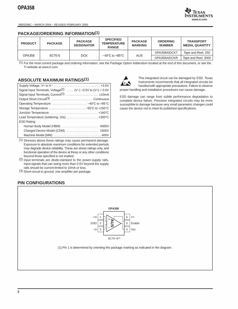
TYPICAL CHARACTERISTICS
All specifications at TA = +25°C, RL = 150Ω connected to VS/2, unless otherwise noted.
200
180
160
140
120
100
80
60
40
20
0
−20
200
180
160
140
120
100
80
60
40
20
0
−20
Ope
n−Lo
opG
ain
(dB
)
Ope
n−Lo
opP
hase
( )
OPEN−LOOP GAIN AND PHASE vs FREQUENCY
100 1k 10k 1M 100M10M100k 1G
Frequency (MHz)
Phase
Gain
1.0
0.5
0
−0.5
−1.0
Nor
mal
ize
dG
ain
(dB
)
GAIN FLATNESS vs FREQUENCY
1 10 100
Frequency (MHz)
G = 2
OFFSET VOLTAGE PRODUCTION DISTRIBUTION
Offset Voltage (mV)
Pop
ula
tion
− 6 − 5 − 4 − 3 − 2 − 1 0 1 2 3 4 5 6
100
80
60
40
20
0
POWER−SUPPLY AND COMMON−MODEREJECTION RATIO vs FREQUENCY
Frequency (Hz)
PS
RR
and
CM
RR
(dB
)
1k 10M1M100k10k 100M
+PSRR
−PSRR
CMRR
1000
100
10
1
INPUT VOLTAGE NOISE SPECTRAL DENSITY
10 100 1k 100k 1M10k 10M
Frequency (Hz)
Vol
tage
Noi
se(n
V/√
Hz)
DIFFERENTIAL GAIN
DIFFERENTIAL PHASE
DG1
INP = C SYNC = INT MTIME = 1 LINE = 330
DG2DG3DG4DG5
%1% .% .% .%5
0 . 1 90 . 2 8
−1 0 +1
0 . 3 00 . 3 00 . 2 8
A
54STEPS
20 1 RESULTSZOOM SAVE
DP1
INP = C SYNC = INT MTIME = 1 LINE = 330
DP2DP3DP4DP5
− 0 . 1 3 d g 10 . 1 6 d g .0 . 4 7 d g .0 . 6 6 d g .0 . 6 9 d g 5
−1 0 +1A
54STEPS
20 1 RESULTSZOOM SAVE
"#$
SB0S296C − MARCH 2004 − REVISED FEBRUARY 2005
www.ti.com
5
TYPICAL CHARACTERISTICS (continued)
All specifications at TA = +25°C, RL = 150Ω connected to VS/2, unless otherwise noted.
8
7
6
5
4
3
2
1
0
Qui
esce
ntC
urre
nt(
mA
)
QUIESCENT CURRENT vs TEMPERATURE
−50 −25 0 50 7525 100
Temperature (C)
10
1
0.1
0.01
0.001
INPUT BIAS CURRENT vs TEMPERATURE
Temperature (C)
Inpu
tBia
sC
urr
ent
(pA
)
−50 7550250−25 100
(V+)
(V+) − 0.5
(V+) − 1.0
(V+) − 1.5
(V−) + 1.5
(V−) + 1.0
(V−) + 0.5
(V−)
OUTPUT VOLTAGE vs OUTPUT CURRENT
Out
putV
olta
ge(V
)
0 20 40 60 80 100
25C
25C
−55C
−55C
85C
85C
Output Current (mA)
3.5
3.0
2.5
2.0
1.5
1.0
0.5
0
SHUTDOWN CURRENT vs TEMPERATURE
Temperature (C)
Sh
utdo
wn
Cu
rren
t(µ A
)
−50 1007550250−25 125
110
100
90
80
70
60
50
40
30
20
10
0
AO
L,P
SR
R,
CM
RR
(dB
)
OPEN−LOOP GAIN, COMMON−MODE REJECTION, ANDPOWER−SUPPLY REJECTION RATIO vs TEMPERATURE
−50 −25 0 50 7525 100
Temperature (C)
AOL
PSRR
CMRR
500
mV
/div
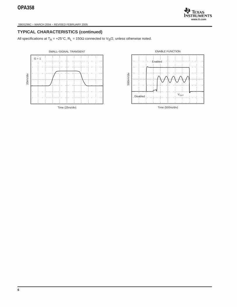
LARGE−SIGNAL TRANSIENT
Time (25ns/div)
G = 2
"#$
SB0S296C − MARCH 2004 − REVISED FEBRUARY 2005
www.ti.com
6
TYPICAL CHARACTERISTICS (continued)
All specifications at TA = +25°C, RL = 150Ω connected to VS/2, unless otherwise noted.
20m
V/d
iv
SMALL−SIGNAL TRANSIENT
Time (25ns/div)
G = 1
500
mV
/div
ENABLE FUNCTION
Time (500ns/div)
Enabled
DisabledVOUT
"#$
SB0S296C − MARCH 2004 − REVISED FEBRUARY 2005
www.ti.com
7
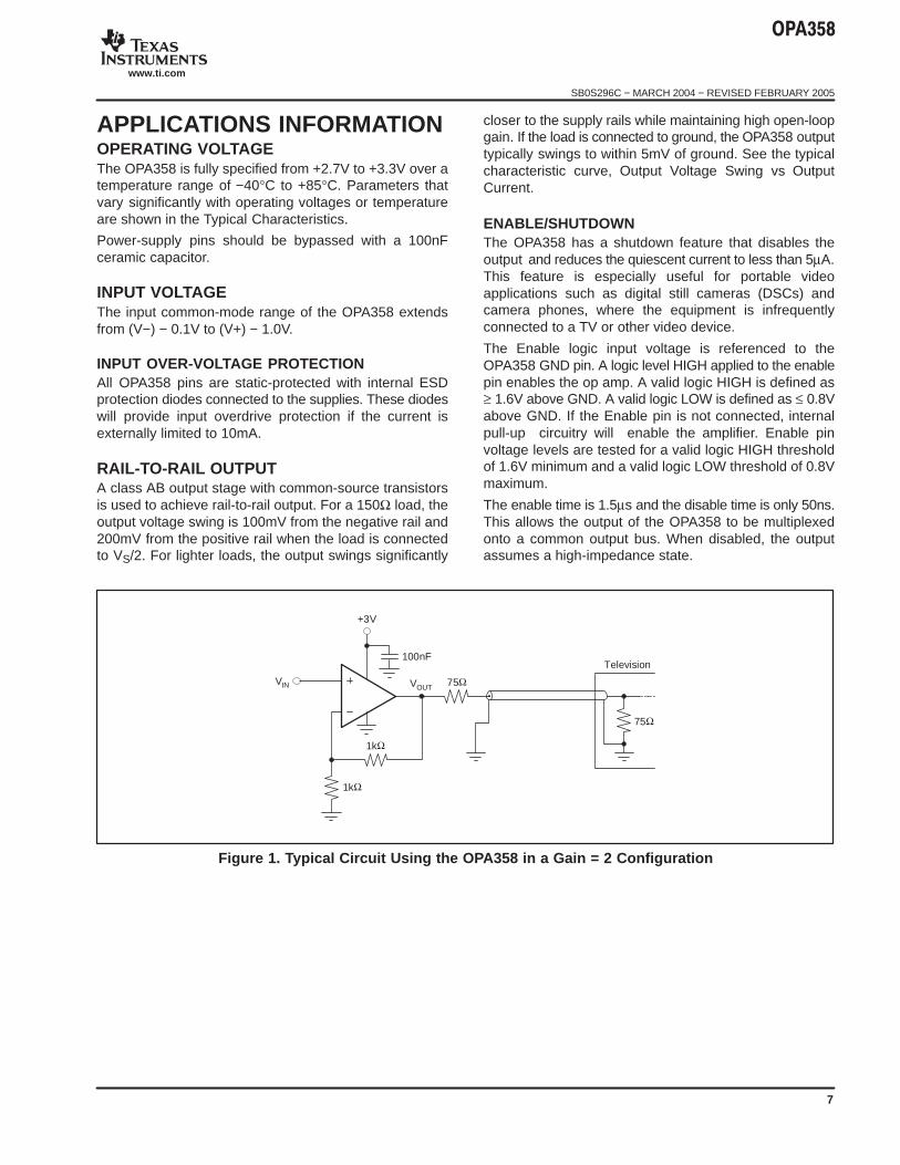
APPLICATIONS INFORMATIONOPERATING VOLTAGEThe OPA358 is fully specified from +2.7V to +3.3V over atemperature range of −40°C to +85°C. Parameters thatvary significantly with operating voltages or temperatureare shown in the Typical Characteristics.
Power-supply pins should be bypassed with a 100nFceramic capacitor.
INPUT VOLTAGEThe input common-mode range of the OPA358 extendsfrom (V−) − 0.1V to (V+) − 1.0V.
INPUT OVER-VOLTAGE PROTECTIONAll OPA358 pins are static-protected with internal ESDprotection diodes connected to the supplies. These diodeswill provide input overdrive protection if the current isexternally limited to 10mA.
RAIL-TO-RAIL OUTPUTA class AB output stage with common-source transistorsis used to achieve rail-to-rail output. For a 150Ω load, theoutput voltage swing is 100mV from the negative rail and200mV from the positive rail when the load is connectedto VS/2. For lighter loads, the output swings significantly
closer to the supply rails while maintaining high open-loopgain. If the load is connected to ground, the OPA358 outputtypically swings to within 5mV of ground. See the typicalcharacteristic curve, Output Voltage Swing vs OutputCurrent.
ENABLE/SHUTDOWNThe OPA358 has a shutdown feature that disables theoutput and reduces the quiescent current to less than 5µA.This feature is especially useful for portable videoapplications such as digital still cameras (DSCs) andcamera phones, where the equipment is infrequentlyconnected to a TV or other video device.
The Enable logic input voltage is referenced to theOPA358 GND pin. A logic level HIGH applied to the enablepin enables the op amp. A valid logic HIGH is defined as≥ 1.6V above GND. A valid logic LOW is defined as ≤ 0.8Vabove GND. If the Enable pin is not connected, internalpull-up circuitry will enable the amplifier. Enable pinvoltage levels are tested for a valid logic HIGH thresholdof 1.6V minimum and a valid logic LOW threshold of 0.8Vmaximum.
The enable time is 1.5µs and the disable time is only 50ns.This allows the output of the OPA358 to be multiplexedonto a common output bus. When disabled, the outputassumes a high-impedance state.
100nF
1kΩ
1kΩ
VOUT 75Ω
75Ω
Television
+3V
VIN
Figure 1. Typical Circuit Using the OPA358 in a Gain = 2 Configuration
"#$
SB0S296C − MARCH 2004 − REVISED FEBRUARY 2005
www.ti.com
8
VIDEO PERFORMANCEIndustry standard video test patterns include: Multiburst—packets of different test frequencies to
check for basic frequency response. Multipulse—pulses modulated at different
frequencies to test for comprehensive measurementof amplitude and group delay errors across the videobaseband.
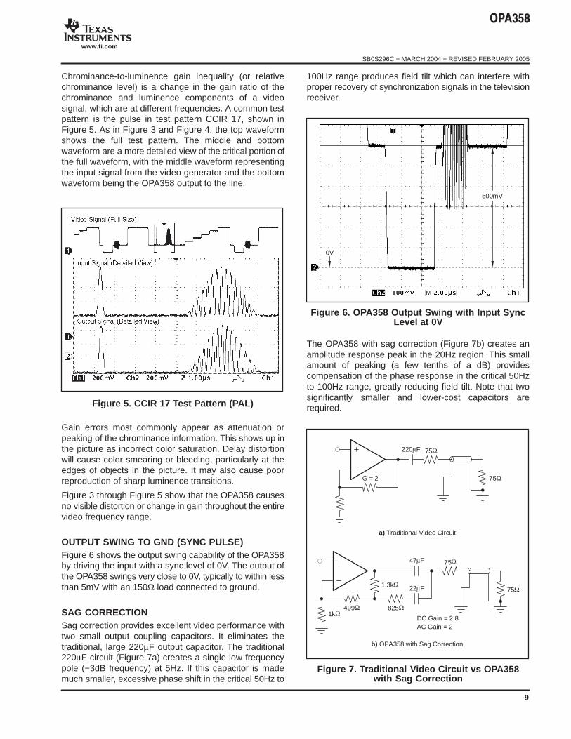
Chrominance-to-luminence (CCIR17) — tests ampli-tude, phase and some distortion
Figure 2 shows the test circuits for Figure 3 throughFigure 13 and Figure 16. (NOTE: 1 and 2 indicatemeasurement points corresponding to the waveformslabeled 1 and 2 in the figures.)
12
a. Test circuit for Figure 3 through Figure 5.
b. Test circuit for Figure 6.
NOTE: 1 and 2 indicate measurement pointscorresponding to the waveforms labeled 1 and2 in the figures.
500Ω
500Ω
12
500Ω
500Ω
Figure 2. Test Circuits Used for Figure 3 throughFigure 6
FREQUENCY RESPONSE OF THE OPA358Frequency response measurements evaluate the ability ofa video system to uniformly transfer signal components ofdifferent frequencies without affecting their respective
amplitudes. Figure 3 shows the multiburst test pattern;Figure 4 shows the multipulse. The top waveforms inthese figures show the full test pattern. The middle andbottom waveform are a more detailed view of the criticalportion of the full waveform. The middle waveformrepresents the input signal from the video generator; thebottom waveform is the OPA358 output to the line.
Figure 3. Multiburst (CCIR 18) Test Pattern (PAL)
Figure 4. Multipulse Test Pattern (PAL)
"#$
SB0S296C − MARCH 2004 − REVISED FEBRUARY 2005
www.ti.com
9
Chrominance-to-luminence gain inequality (or relativechrominance level) is a change in the gain ratio of thechrominance and luminence components of a videosignal, which are at different frequencies. A common testpattern is the pulse in test pattern CCIR 17, shown inFigure 5. As in Figure 3 and Figure 4, the top waveformshows the full test pattern. The middle and bottomwaveform are a more detailed view of the critical portion ofthe full waveform, with the middle waveform representingthe input signal from the video generator and the bottomwaveform being the OPA358 output to the line.
Figure 5. CCIR 17 Test Pattern (PAL)
Gain errors most commonly appear as attenuation orpeaking of the chrominance information. This shows up inthe picture as incorrect color saturation. Delay distortionwill cause color smearing or bleeding, particularly at theedges of objects in the picture. It may also cause poorreproduction of sharp luminence transitions.
Figure 3 through Figure 5 show that the OPA358 causesno visible distortion or change in gain throughout the entirevideo frequency range.
OUTPUT SWING TO GND (SYNC PULSE)Figure 6 shows the output swing capability of the OPA358by driving the input with a sync level of 0V. The output ofthe OPA358 swings very close to 0V, typically to within lessthan 5mV with an 150Ω load connected to ground.
SAG CORRECTIONSag correction provides excellent video performance withtwo small output coupling capacitors. It eliminates thetraditional, large 220µF output capacitor. The traditional220µF circuit (Figure 7a) creates a single low frequencypole (−3dB frequency) at 5Hz. If this capacitor is mademuch smaller, excessive phase shift in the critical 50Hz to
100Hz range produces field tilt which can interfere withproper recovery of synchronization signals in the televisionreceiver.
0V
600mV
Figure 6. OPA358 Output Swing with Input SyncLevel at 0V
The OPA358 with sag correction (Figure 7b) creates anamplitude response peak in the 20Hz region. This smallamount of peaking (a few tenths of a dB) providescompensation of the phase response in the critical 50Hzto 100Hz range, greatly reducing field tilt. Note that twosignificantly smaller and lower-cost capacitors arerequired.
220µF 75Ω
75Ω
a) Traditional Video Circuit
47µF 75Ω
499Ω 825Ω
22µF 75Ω1.3kΩ
1kΩ
b) OPA358 with Sag Correction
G = 2
DC Gain = 2.8AC Gain = 2
Figure 7. Traditional Video Circuit vs OPA358with Sag Correction
"#$
SB0S296C − MARCH 2004 − REVISED FEBRUARY 2005
www.ti.com
10
The output voltage swing for the circuit with sag correction(see Figure 7b) is a function of the coupling capacitorvalue. The value of the sag correction capacitor has onlya minor influence. The smaller the coupling capacitor, thegreater the output swing. Therefore, to accommodate thelarge signal swing with very small coupling capacitors(22µF and 33µF), a higher supply voltage might beneeded.
DC-COUPLED OUTPUTDue to the excellent swing to ground, the OPA358 can alsobe DC- coupled to a video load. As shown in Figure 8, thiseliminates the need for AC-coupling capacitors at theoutput. This is especially important in portable videoapplications where board space is restricted.
The DC-coupled output configuration also shows the bestvideo performance. There is no line or field tilt—allowinguse of the lowest power supply. In this mode, the OPA358will safely operate down to 2.5V with no clipping of thesignal.
The disadvantage with DC-coupled output is that it usessomewhat higher supply current.
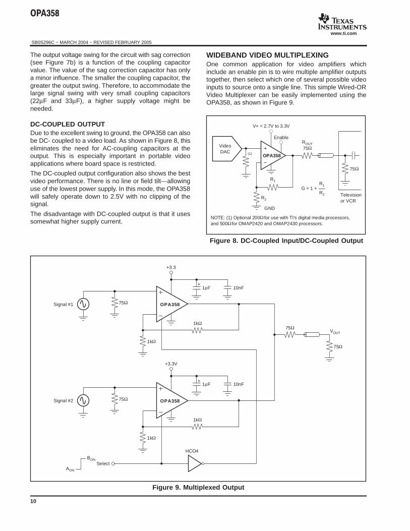
WIDEBAND VIDEO MULTIPLEXINGOne common application for video amplifiers whichinclude an enable pin is to wire multiple amplifier outputstogether, then select which one of several possible videoinputs to source onto a single line. This simple Wired-ORVideo Multiplexer can be easily implemented using theOPA358, as shown in Figure 9.
ROUT75Ω
V+ = 2.7V to 3.3V
Enable
(1)
VideoDAC
NOTE: (1) Optional 200Ω for use with TI’s digital media processors,and 500Ω for OMAP2420 and OMAP2430 processors.
75Ω
R2Televisionor VCR
OPA358
R1
GND
G = 1 +R1
R2
Figure 8. DC-Coupled Input/DC-Coupled Output
1kΩ
OPA358
+3.3
1µF 10nF
75ΩVOUT
75ΩSignal #1
75Ω1kΩ
+
1kΩ
HCO4
OPA358
+3.3V
1µF 10nF
75ΩSignal #2
Select
1kΩ
+
BON
AON
Figure 9. Multiplexed Output

"#$
SB0S296C − MARCH 2004 − REVISED FEBRUARY 2005
www.ti.com
11
CAPACITIVE LOAD AND STABILITYThe OPA358 can drive a wide range of capacitive loads.However, all op amps under certain conditions maybecome unstable. Op amp configuration, gain, and loadvalue are just a few of the factors to consider whendetermining stability. An op amp in unity-gain configurationis most susceptible to the effects of capacitive loading. Thecapacitive load reacts with the op amp output resistance,along with any additional load resistance, to create a polein the small-signal response that degrades the phasemargin.
One method of improving capacitive load drive in theunity-gain configuration is to insert a 10Ω to 20Ω resistorin series with the output, as shown in Figure 10. Thissignificantly reduces ringing with large capacitive loads.However, if there is a resistive load in parallel with thecapacitive load, RS creates a voltage divider. Thisintroduces a DC error at the output and slightly reducesoutput swing. This error may be insignificant. For instance,with RL = 10kΩ and RS = 20Ω, there is only about a 0.2%error at the output.
OPA358
V+
VIN
VOUT
CLRL
RS
To enable,connect to V+
or drive with logic.
Figure 10. Series Resistor in Unity-GainConfiguration Improves Capacitive Load Drive
WIDEBAND TRANSIMPEDANCE AMPLIFIERWide bandwidth, low input bias current, and low inputvoltage and current noise make the OPA358 an idealwideband photodiode transimpedance amplifier forlow-voltage single-supply applications. Low-voltage noiseis important because photodiode capacitance causes theeffective noise gain of the circuit to increase at highfrequency.
The key elements to a transimpedance design, as shownin Figure 11, are the expected diode capacitance(including the parasitic input common-mode anddifferential-mode input capacitance (1.5 + 1.5)pF for theOPA358), the desired transimpedance gain (RF), and theGain Bandwidth Product (GBW) for the OPA358 (80MHz).With these 3 variables set, the feedback capacitor value(CF) may be set to control the frequency response.
OPA358 VOUT
RF10MΩ
CF<1pF
(prevents gain peaking)
+V
λCD
To enable,connect to V+
or drive with logic.
Figure 11. Transimpedance AmplifierTo achieve a maximally flat 2nd-order Butterworthfrequency response, the feedback pole should be set to:
12RFCF
GBW4RFCD
Typical surface-mount resistors have a parasiticcapacitance of around 0.2pF that must be deducted fromthe calculated feedback capacitance value.
Bandwidth is calculated by:
f3dB GBW2RFCD Hz
For even higher transimpedance bandwidth, the CMOSOPA380 (90MHz GBW), OPA355 (200MHz GBW), or theOPA655 (400MHz GBW) may be used.
(1)
(2)

PACKAGE OPTION ADDENDUM
www.ti.com 10-Jun-2014
Addendum-Page 1
PACKAGING INFORMATION
Orderable Device Status(1)
Package Type PackageDrawing
Pins PackageQty
Eco Plan(2)
Lead/Ball Finish(6)
MSL Peak Temp(3)
Op Temp (°C) Device Marking(4/5)
Samples
OPA358AIDCKR ACTIVE SC70 DCK 6 3000 Green (RoHS& no Sb/Br)
CU NIPDAU Level-1-260C-UNLIM -40 to 85 AUS
OPA358AIDCKT ACTIVE SC70 DCK 6 250 Green (RoHS& no Sb/Br)
CU NIPDAU Level-1-260C-UNLIM -40 to 85 AUS
OPA358AIDCKTG4 ACTIVE SC70 DCK 6 250 Green (RoHS& no Sb/Br)
CU NIPDAU Level-1-260C-UNLIM -40 to 85 AUS
(1) The marketing status values are defined as follows:ACTIVE: Product device recommended for new designs.LIFEBUY: TI has announced that the device will be discontinued, and a lifetime-buy period is in effect.NRND: Not recommended for new designs. Device is in production to support existing customers, but TI does not recommend using this part in a new design.PREVIEW: Device has been announced but is not in production. Samples may or may not be available.OBSOLETE: TI has discontinued the production of the device.
(2) Eco Plan - The planned eco-friendly classification: Pb-Free (RoHS), Pb-Free (RoHS Exempt), or Green (RoHS & no Sb/Br) - please check http://www.ti.com/productcontent for the latest availabilityinformation and additional product content details.TBD: The Pb-Free/Green conversion plan has not been defined.Pb-Free (RoHS): TI's terms "Lead-Free" or "Pb-Free" mean semiconductor products that are compatible with the current RoHS requirements for all 6 substances, including the requirement thatlead not exceed 0.1% by weight in homogeneous materials. Where designed to be soldered at high temperatures, TI Pb-Free products are suitable for use in specified lead-free processes.Pb-Free (RoHS Exempt): This component has a RoHS exemption for either 1) lead-based flip-chip solder bumps used between the die and package, or 2) lead-based die adhesive used betweenthe die and leadframe. The component is otherwise considered Pb-Free (RoHS compatible) as defined above.Green (RoHS & no Sb/Br): TI defines "Green" to mean Pb-Free (RoHS compatible), and free of Bromine (Br) and Antimony (Sb) based flame retardants (Br or Sb do not exceed 0.1% by weightin homogeneous material)
(3) MSL, Peak Temp. - The Moisture Sensitivity Level rating according to the JEDEC industry standard classifications, and peak solder temperature.
(4) There may be additional marking, which relates to the logo, the lot trace code information, or the environmental category on the device.
(5) Multiple Device Markings will be inside parentheses. Only one Device Marking contained in parentheses and separated by a "~" will appear on a device. If a line is indented then it is a continuationof the previous line and the two combined represent the entire Device Marking for that device.
(6) Lead/Ball Finish - Orderable Devices may have multiple material finish options. Finish options are separated by a vertical ruled line. Lead/Ball Finish values may wrap to two lines if the finishvalue exceeds the maximum column width.
Important Information and Disclaimer:The information provided on this page represents TI's knowledge and belief as of the date that it is provided. TI bases its knowledge and belief on informationprovided by third parties, and makes no representation or warranty as to the accuracy of such information. Efforts are underway to better integrate information from third parties. TI has taken and
PACKAGE OPTION ADDENDUM
www.ti.com 10-Jun-2014
Addendum-Page 2
continues to take reasonable steps to provide representative and accurate information but may not have conducted destructive testing or chemical analysis on incoming materials and chemicals.TI and TI suppliers consider certain information to be proprietary, and thus CAS numbers and other limited information may not be available for release.
In no event shall TI's liability arising out of such information exceed the total purchase price of the TI part(s) at issue in this document sold by TI to Customer on an annual basis.

TAPE AND REEL INFORMATION
*All dimensions are nominal
Device PackageType
PackageDrawing
Pins SPQ ReelDiameter
(mm)
ReelWidth
W1 (mm)
A0(mm)
B0(mm)
K0(mm)
P1(mm)
W(mm)
Pin1Quadrant
OPA358AIDCKR SC70 DCK 6 3000 179.0 8.4 2.2 2.5 1.2 4.0 8.0 Q3
OPA358AIDCKT SC70 DCK 6 250 179.0 8.4 2.2 2.5 1.2 4.0 8.0 Q3
OPA358AIDCKT SC70 DCK 6 250 178.0 9.0 2.4 2.5 1.2 4.0 8.0 Q3
PACKAGE MATERIALS INFORMATION
www.ti.com 3-Aug-2017
Pack Materials-Page 1

*All dimensions are nominal
Device Package Type Package Drawing Pins SPQ Length (mm) Width (mm) Height (mm)
OPA358AIDCKR SC70 DCK 6 3000 203.0 203.0 35.0
OPA358AIDCKT SC70 DCK 6 250 203.0 203.0 35.0
OPA358AIDCKT SC70 DCK 6 250 180.0 180.0 18.0
PACKAGE MATERIALS INFORMATION
www.ti.com 3-Aug-2017
Pack Materials-Page 2


IMPORTANT NOTICE
Texas Instruments Incorporated (TI) reserves the right to make corrections, enhancements, improvements and other changes to itssemiconductor products and services per JESD46, latest issue, and to discontinue any product or service per JESD48, latest issue. Buyersshould obtain the latest relevant information before placing orders and should verify that such information is current and complete.TI’s published terms of sale for semiconductor products (http://www.ti.com/sc/docs/stdterms.htm) apply to the sale of packaged integratedcircuit products that TI has qualified and released to market. Additional terms may apply to the use or sale of other types of TI products andservices.Reproduction of significant portions of TI information in TI data sheets is permissible only if reproduction is without alteration and isaccompanied by all associated warranties, conditions, limitations, and notices. TI is not responsible or liable for such reproduceddocumentation. Information of third parties may be subject to additional restrictions. Resale of TI products or services with statementsdifferent from or beyond the parameters stated by TI for that product or service voids all express and any implied warranties for theassociated TI product or service and is an unfair and deceptive business practice. TI is not responsible or liable for any such statements.Buyers and others who are developing systems that incorporate TI products (collectively, “Designers”) understand and agree that Designersremain responsible for using their independent analysis, evaluation and judgment in designing their applications and that Designers havefull and exclusive responsibility to assure the safety of Designers' applications and compliance of their applications (and of all TI productsused in or for Designers’ applications) with all applicable regulations, laws and other applicable requirements. Designer represents that, withrespect to their applications, Designer has all the necessary expertise to create and implement safeguards that (1) anticipate dangerousconsequences of failures, (2) monitor failures and their consequences, and (3) lessen the likelihood of failures that might cause harm andtake appropriate actions. Designer agrees that prior to using or distributing any applications that include TI products, Designer willthoroughly test such applications and the functionality of such TI products as used in such applications.TI’s provision of technical, application or other design advice, quality characterization, reliability data or other services or information,including, but not limited to, reference designs and materials relating to evaluation modules, (collectively, “TI Resources”) are intended toassist designers who are developing applications that incorporate TI products; by downloading, accessing or using TI Resources in anyway, Designer (individually or, if Designer is acting on behalf of a company, Designer’s company) agrees to use any particular TI Resourcesolely for this purpose and subject to the terms of this Notice.TI’s provision of TI Resources does not expand or otherwise alter TI’s applicable published warranties or warranty disclaimers for TIproducts, and no additional obligations or liabilities arise from TI providing such TI Resources. TI reserves the right to make corrections,enhancements, improvements and other changes to its TI Resources. TI has not conducted any testing other than that specificallydescribed in the published documentation for a particular TI Resource.Designer is authorized to use, copy and modify any individual TI Resource only in connection with the development of applications thatinclude the TI product(s) identified in such TI Resource. NO OTHER LICENSE, EXPRESS OR IMPLIED, BY ESTOPPEL OR OTHERWISETO ANY OTHER TI INTELLECTUAL PROPERTY RIGHT, AND NO LICENSE TO ANY TECHNOLOGY OR INTELLECTUAL PROPERTYRIGHT OF TI OR ANY THIRD PARTY IS GRANTED HEREIN, including but not limited to any patent right, copyright, mask work right, orother intellectual property right relating to any combination, machine, or process in which TI products or services are used. Informationregarding or referencing third-party products or services does not constitute a license to use such products or services, or a warranty orendorsement thereof. Use of TI Resources may require a license from a third party under the patents or other intellectual property of thethird party, or a license from TI under the patents or other intellectual property of TI.TI RESOURCES ARE PROVIDED “AS IS” AND WITH ALL FAULTS. TI DISCLAIMS ALL OTHER WARRANTIES ORREPRESENTATIONS, EXPRESS OR IMPLIED, REGARDING RESOURCES OR USE THEREOF, INCLUDING BUT NOT LIMITED TOACCURACY OR COMPLETENESS, TITLE, ANY EPIDEMIC FAILURE WARRANTY AND ANY IMPLIED WARRANTIES OFMERCHANTABILITY, FITNESS FOR A PARTICULAR PURPOSE, AND NON-INFRINGEMENT OF ANY THIRD PARTY INTELLECTUALPROPERTY RIGHTS. TI SHALL NOT BE LIABLE FOR AND SHALL NOT DEFEND OR INDEMNIFY DESIGNER AGAINST ANY CLAIM,INCLUDING BUT NOT LIMITED TO ANY INFRINGEMENT CLAIM THAT RELATES TO OR IS BASED ON ANY COMBINATION OFPRODUCTS EVEN IF DESCRIBED IN TI RESOURCES OR OTHERWISE. IN NO EVENT SHALL TI BE LIABLE FOR ANY ACTUAL,DIRECT, SPECIAL, COLLATERAL, INDIRECT, PUNITIVE, INCIDENTAL, CONSEQUENTIAL OR EXEMPLARY DAMAGES INCONNECTION WITH OR ARISING OUT OF TI RESOURCES OR USE THEREOF, AND REGARDLESS OF WHETHER TI HAS BEENADVISED OF THE POSSIBILITY OF SUCH DAMAGES.Unless TI has explicitly designated an individual product as meeting the requirements of a particular industry standard (e.g., ISO/TS 16949and ISO 26262), TI is not responsible for any failure to meet such industry standard requirements.Where TI specifically promotes products as facilitating functional safety or as compliant with industry functional safety standards, suchproducts are intended to help enable customers to design and create their own applications that meet applicable functional safety standardsand requirements. Using products in an application does not by itself establish any safety features in the application. Designers mustensure compliance with safety-related requirements and standards applicable to their applications. Designer may not use any TI products inlife-critical medical equipment unless authorized officers of the parties have executed a special contract specifically governing such use.Life-critical medical equipment is medical equipment where failure of such equipment would cause serious bodily injury or death (e.g., lifesupport, pacemakers, defibrillators, heart pumps, neurostimulators, and implantables). Such equipment includes, without limitation, allmedical devices identified by the U.S. Food and Drug Administration as Class III devices and equivalent classifications outside the U.S.TI may expressly designate certain products as completing a particular qualification (e.g., Q100, Military Grade, or Enhanced Product).Designers agree that it has the necessary expertise to select the product with the appropriate qualification designation for their applicationsand that proper product selection is at Designers’ own risk. Designers are solely responsible for compliance with all legal and regulatoryrequirements in connection with such selection.Designer will fully indemnify TI and its representatives against any damages, costs, losses, and/or liabilities arising out of Designer’s non-compliance with the terms and provisions of this Notice.
Mailing Address: Texas Instruments, Post Office Box 655303, Dallas, Texas 75265Copyright © 2017, Texas Instruments Incorporated