Embed Size (px)
Citation preview

3GPP TR 25.833 V3.0.0 (2003-12)Technical Report
3rd Generation Partnership Project;Technical Specification Group Radio Access Network;
Physical layer items not for inclusion in Release '99(Release 1999)
The present document has been developed within the 3rd Generation Partnership Project (3GPP TM) and may be further elaborated for the purposes of 3GPP. The present document has not been subject to any approval process by the 3GPP Organizational Partners and shall not be implemented. This Specification is provided for future development work within 3GPP only. The Organizational Partners accept no liability for any use of this Specification.Specifications and reports for implementation of the 3GPP TM system should be obtained via the 3GPP Organizational Partners' Publications Offices.

3GPP
3GPP TR 25.833 V3.0.0 (2003-12)2Release 1999
Keywords UMTS, radio, terminal, power
3GPP
Postal address
3GPP support office address 650 Route des Lucioles - Sophia Antipolis
Valbonne - FRANCE Tel.: +33 4 92 94 42 00 Fax: +33 4 93 65 47 16
Internet http://www.3gpp.org
Copyright Notification
No part may be reproduced except as authorized by written permission. The copyright and the foregoing restriction extend to reproduction in all media.
© 2004, 3GPP Organizational Partners (ARIB, CCSA, ETSI, T1, TTA, TTC).
All rights reserved.

3GPP
3GPP TR 25.833 V3.0.0 (2003-12)3Release 1999
Contents Foreword ............................................................................................................................................................4 1 Scope ........................................................................................................................................................5 2 References ................................................................................................................................................5 3 Definitions, symbols and abbreviations ...................................................................................................5 3.1 Definitions ......................................................................................................................................................... 5 3.2 Symbols ............................................................................................................................................................. 6 3.3 Abbreviations..................................................................................................................................................... 6 4 Items not for inclusion in release ’99 .......................................................................................................6 4.1 Transport channels and physical channels (FDD)(TS 25.211) .......................................................................... 7 4.1.1 DSCH Control Channel................................................................................................................................ 7 4.1.2 FAUSCH...................................................................................................................................................... 9 4.1.3 Slow Power Control ................................................................................................................................... 11 4.1.4 USTS.......................................................................................................................................................... 11 4.2 Multiplexing and channel coding (FDD) (TS 25.212)..................................................................................... 12 4.2.1 Hybrid ARQ............................................................................................................................................... 12 4.2.2 Slow Power Control ................................................................................................................................... 12 4.3 Spreading and modulation (FDD) (TS 25.213)................................................................................................ 12 4.3.1 FAUSCH.................................................................................................................................................... 12 4.3.2 Chip rates different from 3.840 Mcps ........................................................................................................ 13 4.3.3 USTS.......................................................................................................................................................... 13 4.4 Physical layer procedures (FDD) (TS 25.214)................................................................................................. 14 4.4.1 FAUSCH.................................................................................................................................................... 14 4.4.2 Slow Power Control ................................................................................................................................... 14 4.4.3 USTS.......................................................................................................................................................... 15 4.5 Physical layer - Measurements (FDD) (TS 25.215)......................................................................................... 16 4.6 Transport channels and physical channels (TDD) (TS 25.221) ....................................................................... 16 4.6.1 RACH half burst ........................................................................................................................................ 16 4.7 Multiplexing and channel coding (TDD) (TS 25.222)..................................................................................... 18 4.7.1 Hybrid ARQ............................................................................................................................................... 18 4.7.2 RACH Channel Coding.............................................................................................................................. 18 4.7.3 SCCC Turbo Coder .................................................................................................................................... 18 4.8 Spreading and modulation (TDD) (TS 25.223) ............................................................................................... 19 4.8.1 Chip rates different from 3.840 Mcps ........................................................................................................ 19 4.9 Physical layer procedures (TDD) (TS 25.224) ................................................................................................ 19 4.9.1 Synchronisation of Cells and ODMA Relays............................................................................................. 19 4.9.2 ODMA Power Control ............................................................................................................................... 20 4.9.3 ODMA Relay Probing................................................................................................................................ 20 4.10 Physical Layer - Measurements (TDD) (TS 25.225) ....................................................................................... 22
Annex A: Change history...............................................................................................................................23

3GPP
3GPP TR 25.833 V3.0.0 (2003-12)4Release 1999
Foreword This Technical Report has been produced by the 3rd Generation Partnership Project (3GPP).
The contents of the present document are subject to continuing work within the TSG and may change following formal TSG approval. Should the TSG modify the contents of the present document, it will be re-released by the TSG with an identifying change of release date and an increase in version number as follows:
Version x.y.z
where:
x the first digit:
1 presented to TSG for information;
2 presented to TSG for approval;
3 or greater indicates TSG approved document under change control.
y the second digit is incremented for all changes of substance, i.e. technical enhancements, corrections, updates, etc.
z the third digit is incremented when editorial only changes have been incorporated in the document.

3GPP
3GPP TR 25.833 V3.0.0 (2003-12)5Release 1999
1 Scope This Technical Report collects material on UTRA physical layer items which have already been in the specifications, but were decided not to be included in release ’99.
The items are described by text from the specifications or by text proposals which have been accepted by WG1.
2 References The following documents contain provisions which, through reference in this text, constitute provisions of the present document.
• References are either specific (identified by date of publication, edition number, version number, etc.) or non-specific.
• For a specific reference, subsequent revisions do not apply.
• For a non-specific reference, the latest version applies.
[1] TS 25.201: “Physical layer – general description”
[2] TS 25.211: “Transport channels and physical channels (FDD)”
[3] TS 25.212: “Multiplexing and channel coding (FDD)”
[4] TS 25.213: “Spreading and modulation (FDD)”
[5] TS 25.214: “Physical layer procedures (FDD)”
[6] TS 25.215: “Physical layer Measurements (FDD)”
[7] TS 25.221: “Transport channels and physical channels (TDD)”
[8] TS 25.222: “Multiplexing and channel coding (TDD)”
[9] TS 25.223: “Spreading and modulation (TDD)”
[10] TS 25.224: “Physical layer procedures (TDD)”
[11] TS 25.225: “Physical layer Measurements (TDD)”
3 Definitions, symbols and abbreviations
3.1 Definitions For the purposes of the present document, the [following] terms and definitions [given in ... and the following] apply.
Definition format
<defined term>: <definition>.
example: text used to clarify abstract rules by applying them literally.

3GPP
3GPP TR 25.833 V3.0.0 (2003-12)6Release 1999
3.2 Symbols For the purposes of the present document, the following symbols apply:
Symbol format
<symbol> <Explanation>
3.3 Abbreviations For the purposes of the present document, the following abbreviations apply:
Abbreviation format
<ACRONYM> <Explanation> ARQ Automatic Repeat Request BCCH Broadcast Control Channel BER Bit Error Rate BLER Block Error Rate BS Base Station CCPCH Common Control Physical Channel DCH Dedicated Channel DL Downlink (Forward link) DPCH Dedicated Physical Channel DPCCH Dedicated Physical Control Channel DPDCH Dedicated Physical Data Channel DS-CDMA Direct-Sequence Code Division Multiple Access FACH Forward Access Channel FDD Frequency Division Duplex FER Frame Error Rate Mcps Mega Chip Per Second ODMA Opportunity Driven Multiple Access OVSF Orthogonal Variable Spreading Factor (codes) PCH Paging Channel PG Processing Gain PRACH Physical Random Access Channel PUF Power Up Function RACH Random Access Channel RX Receive SCH Synchronisation Channel SF Spreading Factor SIR Signal-to-Interference Ratio TDD Time Division Duplex TFCI Transport Format Combination Indicator TFI Transport-Format Indicator TPC Transmit Power Control TX Transmit UE User Equipment UL Uplink (Reverse link) VA Voice Activity
4 Items not for inclusion in release ’99 This section lists text describing the items not for inclusion in R’99.
The text is copied from the specification documents or from text proposals accepted by WG1. Texts are introduced by references, followed by a colon and the text in framed format:

3GPP
3GPP TR 25.833 V3.0.0 (2003-12)7Release 1999
4.1 Transport channels and physical channels (FDD)(TS 25.211)
4.1.1 DSCH Control Channel Sec. 4.2 of V2.1.1:
4.2 Common transport channels
There are six types of common transport channels: BCH, FACH, PCH, RACH, DSCH, and DSCH control channel.
Sec. 4.2.7 of V2.1.1:
4.2.7 DSCH Control Channel
<Note: WG1 concluded that DSCH control channel will not be included in release 99.>
The DSCH control channel is a downlink transport channel carrying control information to the UE for operating the DSCH when not associated with a DCH. Such control information corresponds among other things to resource allocation messages and L1 control information such as TPC, that are not available on the DSCH.
Sec. 5.3.3.4 of V2.1.1:
5.3.3.4 Physical Shared Channel Control Channel (PSCCCH)
<Note: WG1 concluded that PSCCCH will not be included in release 99.>
The frame structure for the PSCCCH is shown in
Figure 1.
Slot #1 Slot #2 Slot #i Slot #15
Frame #1 Frame #2 Frame #i Frame #72
Tslot = 2560 chips, 20*2k bits (k=0..6)
Control informationNdata bits
Tf = 10 ms
Tsuper = 720 ms
Pilot Npilot bits

3GPP
3GPP TR 25.833 V3.0.0 (2003-12)8Release 1999
Figure 1: Frame structure of the Physical Shared Channel Control Channel (PSCCCH).
The PSCCCH contains pilot symbols, and a control information field. The control information field can include TPC commands concerning several users. Other control information includes code assignment for the DSCH, but could also comprise other type of information if needed. The TPC commands would come in support of fast closed loop power control of the PDSCH, and thus, would have to be decoded on a slot-by-slot basis. The exact structure of the control information field is for further study.
Sec. 5.3.3.5.2 of V2.1.1:
5.3.3.5.2 DSCH associated with a DSCH control channel <Note: WG1 concluded that DSCH control channel will not be included in release 99.>
The frame structure of the DSCH when associated with a DSCH control channel is shown in Figure 2.
Slot (2560 chips)
Physical channel 2 (SPCH)PDSCH
PilotPilot Physical channel 1Control information
PSCCCH
Figure 2: Frame structure for the DSCH when associated to a DSCH control channel.
Sec. 6, fig.25 of V2.1.1:
Transport Channels Physical Channels
BCH Primary Common Control Physical Channel (Primary CCPCH)
FACH Secondary Common Control Physical Channel (Secondary CCPCH)
PCH
RACH Physical Random Access Channel (PRACH)
FAUSCH
CPCH
Physical Common Packet Channel (PCPCH)
DCH Dedicated Physical Data Channel (DPDCH)
Dedicated Physical Control Channel (DPCCH)
Synchronisation Channel (SCH)
DSCH Physical Downlink Shared Channel (PDSCH)
DSCH control channel Physical Shared Channel Control Channel (PSCCCH)
Acquisition Indication Channel (AICH)
Page Indication Channel (PICH)
3GPP
3GPP TR 25.833 V3.0.0 (2003-12)9Release 1999
4.1.2 FAUSCH Sec. 4.1, last par. of V2.1.1:
[There are two types of dedicated transport channel, the Dedicated Channel (DCH) and the Fast Uplink Signalling Channel (FAUSCH).]
Sec 4.1.2 of V2.1.1:
4.1.2 FAUSCH – Fast Uplink Signalling Channel <Note: WG1 concluded that FAUSCH will not be included in release 99.>
The Fast Uplink Signalling Channel (FAUSCH) is an optional uplink transport channel that is used to carry control information from a UE. The FAUSCH is always received from the entire cell.
Text proposal of Tdoc TSGR1#4(99)b34 for inclusion in V2.1.1:
5.2.2.3 Physical Fast Uplink Signalling Channel
The Physical Fast Uplink Signalling Channel (PFAUSCH) is used to carry the FAUSCH.
5.2.2.3.1 FAUSCH transmission
5120 chips
AccessSlot #1
Two Frames (20ms)
AccessSlot #15
Figure 5: PFAUSCH access slots
The PFAUSCH consists of 15 access slots, offset in time, by multiples of 5120 chips, from the boundary of every second frame of the received BCH of the current cell. Information on what access slots are available within the current cell is broadcast on the BCH.

3GPP
3GPP TR 25.833 V3.0.0 (2003-12)10Release 1999
256 chipsFast access identifier #1
Fast access identifier #2
Fast access identifier #16
Fast access identifier #17
PFAUSCH access slot boundary
Preamble signature #1
Preamble signature #2
Preamble signature #16
Preamble signature #1
Fast access slot #1 Fast access slot #2No transmission
256 chips
Figure 5: PFAUSCH used for FAUSCH fast access identifiers.
The Fast Uplink Physical Channel (FAUSCH) is based on the transmission of signatures of length 16 complex symbols ±(1+j). The signatures are the same set of signatures used for the RACH preamble. The signatures are spread with a 4096 Long Code, as per the RACH. A fast access identifier, comprising a unique combination of signature and time slot, together with a PFAUSCH access slot number, may be allocated to the UE by the network when entering Connected Mode, but the allocation may be updated with appropriate signalling.
For fast access identifier #i, within a particular PFAUSCH access slot, the assigned fast access slot is given by int(((i-1)/16)+1), and the preamble is (i-1)mod16 + 1.
To avoid the possibility of collisions, only one UE is allowed to transmit with a given signature in a particular time slot. Thus the UE can start the transmission of the FAUSCH at an assigned time offset relative to the boundary of the PFAUSCH access slot. The different time offsets are denoted fast access slots and are spaced 256 chips apart as illustrated in Figure 5. To avoid possible confusion of transmissions from different UEs, the separation between allocations of fast access slots to different UEs with the same signature must be sufficient to allow for any round-trip delay resulting from the physical distance between network and UE. Therefore the allocation of fast access slots may be limited by the network to a subset of those available, depending on the deployment scenario.
Fig. of Tdoc TSGR1#4(99)b34 to replace fig.25 in V2.1.1:
3GPP
3GPP TR 25.833 V3.0.0 (2003-12)11Release 1999
Transport Channels Physical Channels
BCH Primary Common Control Physical Channel (Primary CCPCH)
FACH Secondary Common Control Physical Channel (Secondary CCPCH)
PCH
RACH Physical Random Access Channel (PRACH)
FAUSCH
CPCH
Physical Fast Access Signalling Channel (PFAUSCH)
Physical Common Packet Channel (PCPCH)
DCH Dedicated Physical Data Channel (DPDCH)
Dedicated Physical Control Channel (DPCCH)
Synchronisation Channel (SCH)
DSCH Physical Downlink Shared Channel (PDSCH)
DSCH control channel Physical Shared Channel Control Channel (PSCCCH)
Acquisition Indication Channel (AICH)
Page Indication Channel (PICH)
4.1.3 Slow Power Control New par. in sec. 5.2.1 of V2.2.1 according to Tdoc TSGR1#7(99)c00:
In slow transmit power control, the relationship presented in Table 5 is not valid, and TPC bits are used to carry power control ratio (PCR) as described in 4.3.4 of TS 25.212 and in 5.2.3.3 of TS 25.214.
4.1.4 USTS Last sentence of second par. of sec. 5.3.2 of V3.1.1:
In case of USTS, the TPC bits in slot #14 in frames with CFN mod 2 = 0 are replaced by Time Alignment Bits (TABs) as described in section 9.3 of [5]
Last par. of sec. 7.6.3 of V3.1.1:
In case of USTS, the uplink DPCCH/DPDCH frame transmission for Initial synchronization takes place T0+TINIT_SYNC after the reception of the first significant path of the corresponding downlink DPCCH/DPDCH frame where TINIT_SYNC is Initial synchronization time delivered by UTRAN. However the uplink DPCCH/DPDCH frame transmission for Tracking of USTS takes place approximately T0+TINIT_SYNC±δT after the reception of the first significant path of the corresponding downlink DPCCH/DPDCH frame where δT is the resultant timing adjustment due to the timing control by TAB command bits. More information on TINIT_SYNC and δT can be found in section 9.2 and 9.3 of [5]

3GPP
3GPP TR 25.833 V3.0.0 (2003-12)12Release 1999
4.2 Multiplexing and channel coding (FDD) (TS 25.212)
4.2.1 Hybrid ARQ Sec. 6.3 of S1.22 (V1.1.0):
6.3 Automatic Repeat Request (ARQ) <Editor’s note: this chapter is unchanged from ETSI xx.10 document.>
The details of the UTRA ARQ schemes are not yet specified. Therefore, the impact on layer 1, e.g. if soft combining of retransmitted packets is to take place, is not yet fully specified.
4.2.2 Slow Power Control New sec. in V2.0.1 according to Tdoc TSGR1#7(99)c00:
4.3.4 Coding and Interleaving of power control ratio (PCR) for slow transmit power control When slow transmit power control is used, there are two (encoded) TPC bits in every slot of the radio frame. One PCR is sent in a radio frame, i.e. 30 TPC bits are used. The PCR is firstly encoded using biorthogonal (32, 6) code. The mapping of PCR to the biorthogonal code words, C32,m and C32,m , is defined in TS 25.214. The biorthogonal code words are generated in the same way as OVSF codes of level 32 defined in document TS 25.213. The biorthogonal code words are secondly encoded into PCR code words of 30 bits by puncturing the two least significant bits. Channel interleaving is not applied for the encoded bits, and the bits of the PCR code words are directly mapped to the slots of radio frames so that more significant bit is transmitted before the less significant bit within a radio frame.
4.3 Spreading and modulation (FDD) (TS 25.213)
4.3.1 FAUSCH Text proposal of Tdoc TSGR1#4(99)b34 for inclusion in V2.1.0:
4.3.4 Fast uplink signalling codes
4.3.4.1 Preamble spreading code
Spreading of the FAUSCH preamble is carried out in the same way as for the RACH (4.3.3.1 RACH preamble spreading code).
4.3.4.2 Preamble signature
FAUSCH preamble signatures are the same as those specified for the RACH (4.3.3.2 RACH preamble signature).

3GPP
3GPP TR 25.833 V3.0.0 (2003-12)13Release 1999
<Note: 4.3.4.1 and 4.3.4.2 may need to be rewritten depending on the exact text produced for the relevant RACH sections>
4.3.2 Chip rates different from 3.840 Mcps Table 2 of V2.2.0:
Symbol rate (ksps) spreading No. of Chip rate=
[0.96 Mcps]
3.84 Mcps
[7.68 Mcps]
[15.36 Mcps]
code cycle(chip)SF
Spreading codes
[240] 960 [1920] [3840] 4 4 [120] 480 [960] [1920] 8 8 [60] 240 [480] [960] 16 16 [30] 120 [240] [480] 32 32 [15] 60 [120] [240] 64 64 [7.5] 30 [60] [120] 128 128
- 15 [30] [60] 256 256 - [7.5] [15] [30] 512 512 - - [7.5] [15] 1024 1024 [7.5] 2048 2048
Table 1. Correspondence between Symbol Rate and Spreading Code Types
Sec. 4.4.1 of V2.2.0:
4.4.1 Modulating chip rate The modulating chip rate is 3.84 Mcps. This basic chip rate can be extended to [0.96, ] 7.68 or 15.36 Mcps.
Sec. 5.3.1 of V2.2.0:
5.3.1 Modulating chip rate The modulating chip rate is 3.84 Mcps. This basic chip rate can be extended to [0.96, ] 7.68 or 15.36 Mcps.
4.3.3 USTS Last entry of abbreviations list in sec. 3.2 of V3.1.1:
USTS Uplink Synchronous Transmission Scheme
Last par. of sec. 4.3.1.2 of V3.1.1:
In case of USTS, for the DPCCH, the UTRAN assigns a node number vc (0 ≤ vc ≤ 255) in the code-tree that corresponds to a channelization code of length 256. For a DPDCH, the UTRAN assigns a node number vd (0≤vd≤L-1) in the code-tree that corresponds to a channelization code of length L (i.e., SF for the UE). The sub-tree below the assigned node is used for spreading of DPDCH. When more than one DPDCH is to be transmitted, all DPDCHs have spreading factors

3GPP
3GPP TR 25.833 V3.0.0 (2003-12)14Release 1999
equal to 4. In this case, the UTRAN assigns node numbers vd1, vd2, and vd3 (0 ≤ vd1, vd2, and vd3≤ 3) that correspond to channelization codes of length 4.The DPCCH is always spread by code Cch,0 = Cch,256,k, where k=vc.
- When only one DPDCH is to be transmitted, DPDCH1 is spread by code Cch,SF,k, where SF is the spreading factor of DPDCH1 and k= vd*SF/L.
- When more than one DPDCH is to be transmitted, all DPDCHs have spreading factors equal to 4 (i.e., L=4). DPDCHn is spread by the code Cch,n = Cch,4,k, where k = vd1 if n ∈ {1, 2}, k = vd2 if n ∈ {3, 4}, and k = vd3 if n ∈ {5, 6}.
4.4 Physical layer procedures (FDD) (TS 25.214)
4.4.1 FAUSCH Text proposal of Tdoc TSGR1#4(99)b34 for inclusion in V1.1.0:
4.x PFAUSCH synchronisation
<section to follow 4.4 PRACH synchronisation. No text prepared at this time>
5.1.x PFAUSCH
<section to follow 5.1.1 PRACH on PFAUSCH Power control. No text prepared at this time>
x FAUSCH procedure
<New section "FAUSCH procedure" to be added between sections 6 Random access procedure, and 7 Transmission stop and resumption control. No text prepared at this time.>
4.4.2 Slow Power Control Sec. 5.2.3.3 of V1.1.1 with changes according to Tdoc TSGR1#7(99)c00:
5.2.3.3 Slow transmit power control
Following an order from the network and acknowledgement by the UE, ordinary fast closed-loop transmit power control can be stopped and a slow transmit power control mode can be entered when the UE is not in soft handover. In this mode, downlink DPCCH/DPDCH transmit power is determined utilising power control ratio (PCR) reported from the UE. Uplink transmission is suspended when the UE does not have any information to send, and the transmission is resumed to send PCR at least once in every TRINT second. The UE calculates PCR in the following steps:
1. The UE measures the Ec/Io of the CPICH received from the cell in which the UE is located, and sets the value to Q1.
2. The UE measures the Ec/Io of the CPICH received from the cells belonging to the handover monitoring set, and sets the values greater than Q1/RSEARCH to Qi, where i = 2, 3, …, n.
3. The UE sets the PCR to (Q1 + Q2 + … + Qn)/Q1.

3GPP
3GPP TR 25.833 V3.0.0 (2003-12)15Release 1999
All TPC bits in the uplink DPCCH are used to sendPCR. DPCCH that includes two TPC bits per slot is used. One PCR is sent per frame, i.e. 30 TPC bits are used. Biorthogonal code words, C32,m and C32,m , are used as defined in 4.3.4
of TS 25.212. Code word C32,m corresponds to 0.5(m-1) dB and code word C32,m corresponds to {0.5(m-1)+0.25} dB where m = 1, 2, …, 32. Following an order from the network, the slow transmit power control is stopped and ordinary fast closed-loop transmit power control is started. The parameters TRINT and RSEARCH are set using higher layer signaling.
While uplink transmission is suspended, the TPC commands in downlink DPCCH are all dummy, and are “1”. When uplink transmission is resumed, the UE transmits dummy slots composed of only DPCCH prior to a radio frame composed of DPCCH and DPDCH. The number of the dummy slots is NDS. The TPC commands in the dummy slots are dummy, and are all “1”. When the UE transmits dummy slots, ordinary transmit power control described in 5.1.2.2 is started in uplink transmission.
4.4.3 USTS Sec. 9 of V3.1.1:
9 Uplink synchronous transmission 9.1 General
<Note: This scheme is not a base-line implementation capability.>
UplinkSynchronous Transmission Scheme(USTS) is an alternative technology applicable for low mobility terminals. USTS can reduce uplink intra-cell interference by means of making a cell receive orthogonalized signals from UEs. To orthogonalize receiving signals from UEs,
- the same scrambling code is allocated to all dedicated physical channels in a cell,
- different channelization codes are allocated to all dedicated physical channels across all UEs in a cell and the spreading factor and code number of channelization code are delivered from network to each UE
- the channelization codes for DPDCH and DPCCH in a UE are chosen from either upper half part or the lower half part of the OVSF code tree in a UE to reduce peak to average power ratio,
- additional scrambling codes can be allocated if all channelization codes are occupied, and
- the signal transmission time of each UE is adjusted.
The spreading and modulation scheme for USTS is same as section 4 of TS 25.213. In case of USTS, the long scrambling code described in section 4.3.2.2. of TS 25.213 is used. However, this long scrambling code is not UE specific, but cell specific. In order to generate the cell specific long scrambling code, the initial loading value of PN generator is determined by the network
The channelization codes are Orthogonal Variable Spreading Factor (OVSF) codes that preserve the orthogonality between USTS uplink channels of different rates and spreading factors.
The transmission time control is carried out by two steps. The first step is initial synchronization and the second is tracking.
1) Initial synchronization: Adjust transmission time through the initial timing control message over FACH
2) Tracking Process (Closed Loop Timing control): Adjust the transmission time through the Time Alignment Bit (TAB) over DPCCH.
9.2 Initial synchronisation - When the cellreceives signal from UE over RACH, cell measures the difference in time between the received
timing and the reference time in the unit of 1/8 chip duration..

3GPP
3GPP TR 25.833 V3.0.0 (2003-12)16Release 1999
- The message for initial synchronization, which contains the difference in time, is delivered to UE via FACH.
- UE adjust its transmission time according to the message.
9.3 Tracking process - Cell periodically compares the reference time with received signal timing from UE.
- When the received timing is earlier than the reference time, Time Alignment Bit (TAB) = "0". When this is later than the reference time, TAB = "1".
- TAB replaces the TPC bit every timing control period of 20 msecand the last TPC bit of every two frames is replaced by TAB.
- At the UE, hard decision on the TAB shall be performed, and when it is judged as "0", the transmission time shall be delayed by 1/8 chip, whereas if it is judged as "1", the transmission time shall be advanced by 1/8 chip.
4.5 Physical layer - Measurements (FDD) (TS 25.215)
4.6 Transport channels and physical channels (TDD) (TS 25.221)
4.6.1 RACH half burst Sec. 5.3.2 of V1.1.1:
5.3.2 The physical random access channel (PRACH) The RACH or in case of ODMA networks the ORACH as described in section エラー! 参照元が見つかりません。 are mapped onto one or more uplink physical random access channels (PRACH). In such a way the capacity of RACH and ORACH can be flexibly scaled depending on the operators need.
This description of the physical properties of the PRACH also applies to bursts carrying other signaling or user traffic if they are scheduled on a time slot which is (partly) allocated to the RACH or ORACH.
5.3.2.1 Spreading codes
The uplink PRACH uses fixed spreading with a spreading factors SF=16 or SF=8 as described in section エラー! 参照元が見つかりません。. The set of admissible spreading codes for use on the PRACH and the associated spreading factors are broadcasted on the BCH (within the RACH configuration parameters on the BCH, see Ref.[3])
5.3.2.2 Burst Types
The mobile stations send the uplink access bursts randomly in the PRACH. Two distinct access bursts are defined which effectively devide a 625µs ("full") time-slot into two 312.5µs ("half") slots. The access bursts 1 and 2 occupy the first and the second half slot, respectively. The access bursts of type 1 and 2 coexist in a full time slot: they never collide with each other.Depending on the RACH configuration broadcasted on the BCH, up to 8 different mobile stations can access on the same half slot simultaneously without colliding. The precise number of collision groups depends on the set of admissible midambles and spreading codes (i.e. the selected RACH configuration. The access bursts are depicted in エラー! 参照元が見つかりません。 and エラー! 参照元が見つかりません。 and the contents of the access burst fields are listed in エラー! 参照元が見つかりません。 and エラー! 参照元が見つかりません。.
Table 2 The contents of the access burst 1 fields

3GPP
3GPP TR 25.833 V3.0.0 (2003-12)17Release 1999
Chip Number (CN) Length of field in chips
Length of field in symbols
Length of field in µs Contents of field
0-335 336 21 82.0 Data symbols
336-847 512 - 125.0 Midamble
848-1183 336 21 82.0 Data symbols
1184-1279 96 - 23.4 Guard period
1279-2559 1280 - 312.5 Extended guard period
Extended GPData Midamble GPData
312.5 µs 312.5 µs
625 µs Figure 3 Access burst 1, GP denotes the guard period
Table 3 The contents of the access burst 2 fields
Chip Number (CN) Length of field in chips
Length of field in symbols
Length of field in µs Contents of field
0-1279 1280 - 312.5 Extended guard period
1280-1615 336 21 82.0 Data symbols
1616-2127 512 - 125.0 Midamble
2128-2463 336 21 82.0 Data symbols
2464-2559 96 - 23.4 Guard period
Extended GP Data Midamble GPData
625 µs
312.5 µs 312.5 µs
Figure 4 Access burst 2, GP denotes the guard period
3GPP
3GPP TR 25.833 V3.0.0 (2003-12)18Release 1999
5.3.2.3 Training sequences for access bursts The training sequences, i.e. midambles, of different users active in the same half time slot are time shifted versions of a small set of periodic basic codes (in cells with small radius, a single periodic code can be used). The necessary time shifts are obtained by choosing either all k=1,2,3...,K (for cells with small radius) or uneven k=1,3,5,...≤K (for cells with large radius, as explained in Sect. 6.2.3.1). Different cells use different periodic basic codes, i.e. different midamble sets. In this way, a joint channel estimation for the channel impulse responses of all active users within one half time slot can be performed by a small number of cyclic correlations (in cells with small radius, a single cyclic correlator suffices). The different user specific channel impulse response estimates are obtained sequentially in time at the output of the cyclic correlators.
4.7 Multiplexing and channel coding (TDD) (TS 25.222)
4.7.1 Hybrid ARQ Sec. 6.3 of S1.22 (V1.1.0):
6.3 Automatic Repeat Request (ARQ) <Editor’s note: this chapter is unchanged from ETSI xx.10 document.>
The details of the UTRA ARQ schemes are not yet specified. Therefore, the impact on layer 1, e.g. if soft combining of retransmitted packets is to take place, is not yet fully specified.
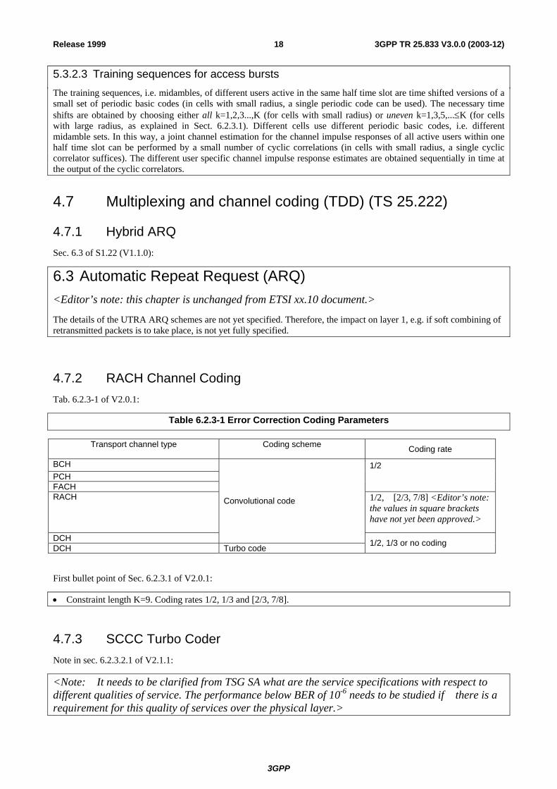
4.7.2 RACH Channel Coding Tab. 6.2.3-1 of V2.0.1:
Table 6.2.3-1 Error Correction Coding Parameters
Transport channel type
Coding scheme Coding rate
BCH PCH FACH
1/2
RACH 1/2, [2/3, 7/8] <Editor’s note: the values in square brackets have not yet been approved.>
DCH
Convolutional code
DCH Turbo code 1/2, 1/3 or no coding
First bullet point of Sec. 6.2.3.1 of V2.0.1:
• Constraint length K=9. Coding rates 1/2, 1/3 and [2/3, 7/8].
4.7.3 SCCC Turbo Coder Note in sec. 6.2.3.2.1 of V2.1.1:
<Note: It needs to be clarified from TSG SA what are the service specifications with respect to different qualities of service. The performance below BER of 10-6 needs to be studied if there is a requirement for this quality of services over the physical layer.>

3GPP
3GPP TR 25.833 V3.0.0 (2003-12)19Release 1999
4.8 Spreading and modulation (TDD) (TS 25.223)
4.8.1 Chip rates different from 3.840 Mcps Table 1 of V2.2.0:
Table 1: Basic modulation parameters.
Chip rate same as FDD basic chiprate, 3.84 Mchip/s
[( 7.68,15.360 Mcps)]
Low chiprate:
Value is FFS
Data modulation QPSK QPSK
Spreading characteristics Orthogonal
Q chips/symbol, where Q = 2p, 0 <= p <= 4
Orthogonal
Q chips/symbol, where Q = 2p, 0 <= p <= 4
4.9 Physical layer procedures (TDD) (TS 25.224)
4.9.1 Synchronisation of Cells and ODMA Relays Sec. 4.2 of V1.1.1:
4.2 Synchronisation of Cells and ODMA Relays
4.2.1 Synchronisation of TDD Cells
In several scenarios, there is a need to synchronise Node Bs in order to optimise system capacity. One example is a scenario for coordinated operation with overlapping coverage areas of the cells, i.e. there is contiguous coverage for a certain area.
Several alternatives can be used to synchronise Cells . The 3GPP TS25.2xx specification shall provide the means for Cell synchronisation by an air interface protocol.
< Editors note: The specification of this Cell synchronisation protocol is for further study and depends on required synchronisation accuracy. The protocol shall fulfil the following requirements:
• Reliability and stability
• Low implementation effort
• Minimum impact on air interface traffic capacity.
For example the two schemes below are considered in WG1:
1. For Cell synchronisation via the air interface a special burst, the network synchronisation burst, is used. This burst is sent on a predetermined TS at regular intervals. During the reception of the network synchronisation burst in a cell the transmission in this cell has to be switched off. The UTRAN receives this burst and adjusts the frame timing in the cells accordingly.
2. Cells are synchronised by means of receiving other cells Physical Synchronisation Channel (PSCH). >
4.2.1.1 Inter-system-synchronisation
<Editors Note: to be determined>
3GPP
3GPP TR 25.833 V3.0.0 (2003-12)20Release 1999
4.2.2 Synchronisation of ODMA Relays Due to the relatively short range of transmissions, the inclusion of ODMA does not impose any additional guard period or frame synchronisation requirements over those discussed above for standard TDD.
Any potential overlap caused by relay transmissions will be localised to a node and its neighbours by the ODMA protocol.
The inclusion of ODMA could relax the guard period requirements when relaying between nodes (not involving the BS) since neighbouring UEs are regarded as relay opportunities and any communications between neighbours (on an ODCH) could be synchronised further
4.9.2 ODMA Power Control Sec. 4.3.2 of V1.1.1:
4.3.2 ODMA Power Control <for further study>
4.9.3 ODMA Relay Probing Sec. 4.5 of V3.1.0:
4.5 ODMA Relay Probing This section describes the probe-response procedure used by ODMA nodes to detect neighbours which may be used as relays during a call.
4.5.1 Initial Mode Probing The initial mode probing procedure is activated by a UE when it is switched on and has no information about its surroundings. In this case the UE will synchronise with the ODMA Random Access Channel (ORACH) which is used by all UEs to receive and broadcast system routing control information and data. The UE begins a probing session by periodically broadcasting a probe packet on the ORACH. The broadcast probe includes the current neighbour list for the UE which will initially be empty. If a neighbouring UE, UEa, receives the broadcast packet it will register the UE as a neighbour and send an addressed response probe. The response probe is transmitted at random to avoid contention with other UEs and typically one response is sent for every n broadcast probes received from a particular UE.
The next time the UE transmits a broadcast probe the neighbour list will have one new entry, UEa, and an associated quality indicator (a weighted factor based on the received signal strength of the response probe). It is through this basic mechanism that each UE builds a neighbour list.
4.5.2 Idle Mode Probing The Idle Mode Probing procedure is activated when the UE has synchronised with the ORACH but is not transmitting data. This procedure is the same as that described above after ORACH synchronisation.
The ODMA Idle Mode Probing procedure controls the rate of probing on the ORACH to reduce interference levels and regulate power consumption. The procedure is governed by a state machine, which consists of the following states: full probing, duty maintained probing, and relay prohibited. Each state defines the number of probing opportunities within one N multiframe, and a probing activity parameter K which is the ratio of probe transmission time to probe monitoring time.
Full probing
Full probing is the case where probing is allowed on every ORACH timeslot within an N multiframe. The UER will probe on the ORACH at a rate defined by the probing activity parameter K.

3GPP
3GPP TR 25.833 V3.0.0 (2003-12)21Release 1999
Duty Maintained probing
The duty maintained probing is the case where probing is allowed on M slots of an N multiframe. The UER will probe on the M ORACH slots in an N multiframe at a rate defined by the probing activity parameter K.
Relay Prohibited
In this mode the UER would cease all of its ODMA probing activities and will fall into standard TDD or FDD operation.
The probing activity levels for given state machines are illustrated in Figure 1 for a system with an ORACH for M slots per N × 16 multiframe.
Note that the distribution of probing opportunities within a multiframe may not necessarily be consecutive and located at the beginning of a multiframe.
TxRxTxRx
(b) Duty maintained probing - example
RxTxRxTxTxRxTxRx RxTx RxTxRxTx
(a) Full probing
N frame multiframe (e.g. M=N, K= 0.5 )
N frame multiframe (e.g. 0<M<=N, K= 0.5)
(c) Relay prohibited
N frame multiframe (e.g. M= 0)
TN0 TN1 TN14
CCPCH
ORACH
10 ms
Figure 1: Probing state machines and mechanism
4.5.3 Active Mode Probing The Active Mode Probing procedure is activated when the UE has synchronised with the ORACH and is transmitting data.
With ODMA, data may be relayed on either the ODMA Random Access Channel (ORACH) or the ODMA dedicated transport channel (ODCH), depending on the volume of data to be sent. When a UE has small amounts of data to send it may transmit an addressed probe response packet on the ORACH at an interval proportional to air interface modem rate, RCCH, and is defined by Probe_timer_1. This interval also defines the broadcast probe interval, Probe_timer_2, which is typically five times longer than Probe_timer_1. Every time an UE transmits a response probe containing data on the ORACH, it may be received, but not acknowledged, by third party neighbour UEs, and provides an implicit indication of activity. In this instance broadcast probes are not necessary and Probe_timer_2 is reset after every addressed probe transmission. Only when an UE has no data to send is it necessary to transmit a broadcast probe every Probe_timer_2 seconds to register its active status with its neighbours.
In order to avoid overlapping packet transmissions the length of the packet may not exceed the probe timer interval, Probe_timer_1. The relationship between the different probe timers is illustrated in Figure 2.

3GPP
3GPP TR 25.833 V3.0.0 (2003-12)22Release 1999
Probe_timer_1 α CCH data rate, RCCH
Broadcast timer, Probe_timer_2 = 5*Probe_timer_1
Maximum packet length = Probe_timer_1*RCCH
CCH data txopportunities
Tx CCH broadcast
probe
Figure 2: Probe timer relationships
4.10 Physical Layer - Measurements (TDD) (TS 25.225)

3GPP
3GPP TR 25.833 V3.0.0 (2003-12)23Release 1999
Annex A: Change history
Change history Date TSG # TSG Doc. CR Rev Subject/Comment Old New
02/09/99 - - - - First version based on WG1 minutes, specifications, text proposals and WG1 discussion on the document’s scope.
- 0.0.1
07/09/99 R1_07 - - - Version agreed with the following modifications at 7th WG1 meeting at Hanover: Note on SCCC Turbo Coder included, chip rates different from 3.84 Mcps included.
0.0.1 0.1.0
15/12/99 RP_06 - - - First version agreed by RAN. Name changed to TR 25.833
0.1.0 1.0.0
15/04/00 R1_12 - - - Version agreed by WG1 at 12th meeting at Seoul. Reference [11] corrected.
1.0.1 1.1.0
19/12/04 RP_22 RP-030645 - - Presented to RAN and approved.to place under version control as a Release 1999 Technical Report
2.0.0 3.0.0