Embed Size (px)
Citation preview

3D TECHNOLOGIES:
SOME PERSPECTIVES FOR MEMORY
INTERCONNECT AND CONTROLLER
CODES+ISSS: Special session on memory controllers
Taipei, October 10th 2011
Denis Dutoit, Fabien Clermidy, Pascal Vivet {[email protected]}

© CEA. All rights reserved
D. Dutoit, CODES+ISSS, Taipei | Oct 10th, 2011 | 2
3D-IC design: will dream become reality ?
� Example of an heterogeneous 3D-IC stack:
RF/AnalogProc
Mem
DRAM
Proc
NVM
Active interposer (mature technology): Services & communication infrastructure ; IO with ESD; Test; Supply distribution; Power management
Standard DRAM
Parallel & low speed IF
Stackable Processor
Standard Non Volatile Memory
Serial high speed IF
� This presentation focuses on vertical interconnect
between complex MPSoC and memory

© CEA. All rights reserved
D. Dutoit, CODES+ISSS, Taipei | Oct 10th, 2011 | 3
Outline
� Introduction
� 3D TSV technology choices� 3D-IC toolbox
� Design perspectives
� Improving memory bandwidth� The memory link bottleneck
� Overview of memory interfaces: bandwidth, power consumption,
package integration
� Wide IO interface integration: Mag3D circuit� Wide IO technology
� Mag3D circuit: architecture, Wide IO DRAM integration, design
implementation challenges and current results
� Conclusion & perspectives

© CEA. All rights reserved
D. Dutoit, CODES+ISSS, Taipei | Oct 10th, 2011 | 4
Outline
� Introduction
� 3D TSV technology choices� 3D-IC toolbox
� Design perspectives
� Improving memory bandwidth� The memory link bottleneck
� Overview of memory interfaces: bandwidth, power consumption,
package integration
� Wide IO interface integration: Mag3D circuit� Wide IO technology
� Mag3D circuit: architecture, Wide IO DRAM integration, design
implementation challenges and current results
� Conclusion & perspectives
© CEA. All rights reserved
D. Dutoit, CODES+ISSS, Taipei | Oct 10th, 2011 | 5
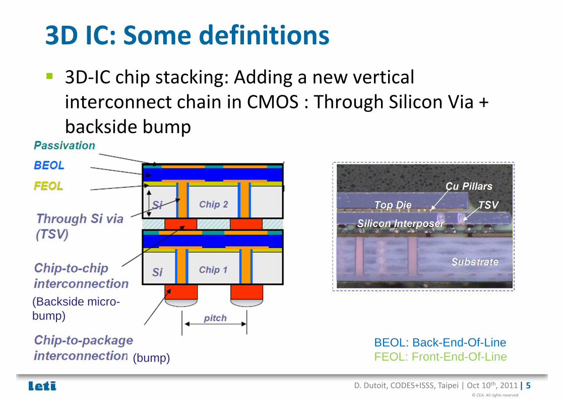
3D IC: Some definitions
� 3D-IC chip stacking: Adding a new vertical
interconnect chain in CMOS : Through Silicon Via +
backside bump
(Backside micro-bump)
(bump)BEOL: Back-End-Of-LineFEOL: Front-End-Of-Line

© CEA. All rights reserved
D. Dutoit, CODES+ISSS, Taipei | Oct 10th, 2011 | 6
3D IC interconnect: Through Silicon Via
Via First TSV (Polysilicon filled)Trench AR 20, 5x100µmProcessed before CMOS front-end steps
Pitch: ~10µmDensity: 10000 TSV/mm²
AR 7 , 2 x 15µm
Via Middle TSV (Copper filled)
AR 10, 10x100µm
Processed after CMOS front-end stepsPitch: 40µm to 50µmDensity: 500 TSV/mm²
Via Last TSV (Copper liner)
AR 1 80x80µm
AR 2, 60x120µm
SiO2 flanc
métal RDL
BCB
bulle air sous BCB
60
µm
AR 3, 40x120µm
Processed after metallizationPitch: ~100µmDensity: 100 TSV/mm²

© CEA. All rights reserved
D. Dutoit, CODES+ISSS, Taipei | Oct 10th, 2011 | 7
3D IC interconnect: inter-chip connections
Pitch
Classic Flip chip (Ball or stud bump)
> 100 µm
TSV last
Solder-free µinserts
Cu pillars
Nickel Microinsertion
100-30 µm range
SnAg Solder
TSV middle
Cu-Cu Direct bonding
Si
Si
Cu
SiO2
Si
Si
Cu
SiO2
Need very flat surfaceCleaning
µtubes
Down to 5 µm30-10 µm range
Microinsertion
TSV first

© CEA. All rights reserved
D. Dutoit, CODES+ISSS, Taipei | Oct 10th, 2011 | 8
Current TSV technology and design
perspectives1. What can we expect ?
� 10 µm diameter TSV is
challenging
� Must add guard interval
� Die thickness is an issue
2. 3D design is not yet
mature:
� No accurate CAD tools &
models for 3D (CTS,
extraction, Thermal, Power …)
� No accurate test model for
TSV
� Resulting 3D partitioning ?
� Fine grain partitioning of an
operator in two dies using TSV
is not a good option
⇒ Coarse grain to medium grain
partitioning
⇒Proposal ? 3D Memory (Wide IO)

© CEA. All rights reserved
D. Dutoit, CODES+ISSS, Taipei | Oct 10th, 2011 | 9
Outline
� Introduction
� 3D TSV technology choices� 3D-IC toolbox
� Design perspectives
� Improving memory bandwidth� The memory link bottleneck
� Overview of memory interfaces: bandwidth, power consumption,
package integration
� Wide IO interface integration: Mag3D circuit� Wide IO technology
� Mag3D circuit: architecture, Wide IO DRAM integration, design
implementation challenges and current results
� Conclusion & perspectives

© CEA. All rights reserved
D. Dutoit, CODES+ISSS, Taipei | Oct 10th, 2011 | 10
The memory link bottleneck
� The transfer Bandwidth between
Memory and processor always
been an issue for computing:
� BW = nb of bits x bit rate
� The needs of computing:
� 2014: 1TB/s
� For Mobile Computing
architecture is more constraining,
both Graphic and system
memory on same support
� The needs of Mobile computing:
� 2010: 4GB/s
� 2012: 12GB/s
� 201X: 100GB/s
Computing Scheme [Intel Journal Aug 2007]

© CEA. All rights reserved
D. Dutoit, CODES+ISSS, Taipei | Oct 10th, 2011 | 11
Standardization evolves to 3D stacked memory
� JEDEC JC-42.6 Subcommittee for Low Power Memories:
� LPDDR2, LPDDR3, WideIO
� LPDDR2:
� Advanced power management features
� Shared interface for nonvolatile memory (NVM) and volatile
memory (SDRAM)
� LPDDR3:
� Extension of LPDDR2
� Bandwidth reaching 6.4GBps and allowing 12.8GBps for a dual
channel configuration.
� Supports POP packaging type
� WideIO:
� Breakthrough technology
� Uses chip-level three dimensional (3D) stacking with TSV
interconnects
� Bandwidth is 12.8GBps
Information from JEDEC web site
GB/s

© CEA. All rights reserved
D. Dutoit, CODES+ISSS, Taipei | Oct 10th, 2011 | 12
IO and power cost for a 100GB/s memory bandwidth
� 3D integration of DRAM memory on processor with wide data
interconnects provides higher data throughput and lower power
consumption than 2D interfaces.
Memory link, peak bandwidth and power consumption e fficiency
Cost for 100 GB/s memory bandwidth
Number of data IO pins
Interface power consumption
4.264 GB/s~20 mW/Gb/s
533 MHz I/O bus clock, 32 bits, 1.2 V, Double Data Rate
770 16 W
6.4 GB/s<20 mW/Gb/s
800 MHz I/O bus clock, 32 bits, 1.2V, Double Data Rate
770 <16 W
12.8 GB/s4 mW/Gb/s
200 MHz I/O bus clock, 512 bits, 1.2 V, Single Data Rate
4100 3.2 W
Multi-coreSoC DRAMLPDDR3
Multo-coreSoC DRAMWide I/O
Multi-coreSoC
DRAMLPDDR2

© CEA. All rights reserved
D. Dutoit, CODES+ISSS, Taipei | Oct 10th, 2011 | 13
Memory-interface package evolution
Multi-core SoC
Off-Package
DDR3
POP Package
LPDDR2 / LPDDR3
Wide I/O DRAM
3D IC with TSVs

© CEA. All rights reserved
D. Dutoit, CODES+ISSS, Taipei | Oct 10th, 2011 | 14
Outline
� Introduction
� 3D TSV technology choices� 3D-IC toolbox
� Design perspectives
� Improving memory bandwidth� The memory link bottleneck
� Overview of memory interfaces: bandwidth, power consumption,
package integration
� Wide IO interface integration: Mag3D circuit� Wide IO technology
� Mag3D circuit: architecture, Wide IO DRAM integration, design
implementation challenges and current results
� Conclusion & perspectives

© CEA. All rights reserved
D. Dutoit, CODES+ISSS, Taipei | Oct 10th, 2011 | 15
Wide IO technology� Low power DRAM technology
� 12.8GByte/s peak bandwidth
� ~500mW power
� Quad-channel interface with large data bus operating
at low frequency:
� 128 bit wide data bus
� Single Data Rate sampling mode @200MHz
� Separate power-down & self-refresh per channel
� Timing performances:
� Same as SDR 200MHz
� 1.2V low voltage supply
� Total I/O count including supply is in the range of
~1200:
� IO physical location standardized at Jedec
� 4 Arrays of 50x6; Pitch: 50µm x 40µm
� Placed in the center area of the memory die
� Boundary scan test mode to detect bump connection
failure between chips.
� Maximum number of stacked dies is 4
Bank 0
Channel 0 Channel 1
Channel 2 Channel 3
Bank 2
Bank 1
Bank n
Bank 0
Bank 2
Bank 1
Bank n
Bank 0
Bank 2
Bank 1
Bank n
Bank 0
Bank 2
Bank 1
Bank n
Wide IO DRAM floorplan
Cu Pillars
TSV middle
Metal stack
Wide IO DRAM: face down
SoC: face down
PackageSubstrate
Metal stack
Package Balls
Packagemolding
3D-IC with Wide IO DRAM
Interconnect area

© CEA. All rights reserved
D. Dutoit, CODES+ISSS, Taipei | Oct 10th, 2011 | 16
Mag3D test chip program
� Partnership between LETI, STEricsson,
STMicroelectronics and Cadence
� Wide IO DRAM die is stacked on top of the
SoC (Mag3D) in the same package
� Face to Back stacking
� Memory supplies and interconnect signals go
through the SoC by means of TSVs
Central array of µbumps
Metal stack
Wide IO DRAM: face down
SoC: face down
PackageSubstrate
sign
al
SDRAMsupply IOs
SoC signal and supply IOs,SDRAM muxed test IOs
supp
lyPeripheral bumps Central matrix
µ-buffersupply IOs
VD
DQ
supp
ly
Metal stack
Package Balls
Packagemolding
1250 TSVs
985 bumps
475 balls
1250 µ-bumps
SoC signal and supply IOs,SDRAM muxed test IOs
Technology assumptions
Assembly D2D
Stacking F2B
TSV process Via Middle
TSV density 10µm diameter
TSV xy pitch 50µm x 40 µm
Copper Pillars 25µm diameter

© CEA. All rights reserved
D. Dutoit, CODES+ISSS, Taipei | Oct 10th, 2011 | 17
Wide IO integration into Mag3D� 3D test chip baseline is the 65nm LETI MAGALI SoC
� The NoC architecture has been extended to support Wide IO memory
� Four independent data traffic and memory controllers have been added
30
20
10
00
3D(ftol)
TX_BITtx_bit00n
31
21
11
01
32
22
12
02
33
23
13
03
2 4 2
6 1 6
6 1 6
2 4 2
2
6
2
5 4 4 4
6 5 5 6
6 3 4 4
1
MEPHISTOmep_01n
MEPHISTOmep_02n
TRX_OFDMtrx_ofdm_03nTRX_OFDMtrx_ofdm_03n
ARM11arm11_00w
TRX_OFDMtrx_ofdm_03eTRX_OFDMtrx_ofdm_03e
SMEsme_01
SMEsme_03
SME_EXTsme_10
UDECASIPasip_13
UDECASIPasip_13
SME_WIDEIOSME_WIDEIOsme_11
SME_WIDEIOSME_WIDEIOsme_12
SME_WIDEIOSME_WIDEIOsme_22
SME_WIDEIOSME_WIDEIOsme_21
RX_BITrx_bit23
SMEsme_31
SMEsme_33
MEPHISTO_
mep_30w
MEPHISTO_HEATERmep_30w
MEPHISTOmep_33e
MEPHISTOmep_33s
MEPHISTOmep_32s
TRX_OFDMtrx_ofdm_30sTRX_OFDMtrx_ofdm_30s
TRX_OFDMtrx_ofdm_31sTRX_OFDMtrx_ofdm_31s
nocif2
nocif1
3D(serial2)
3D(serial2r)
3D(normal)
TEST3DNoC
TESTWide IO
Channel 0
Channel 1
Channel 2
Channel 3
Wide IO
SD
RA
M 4x128-bit channel -
166Mhz
Data traffic&
Channel 0Controller
µ-Buffer
ES
D
NIF
Test
Data traffic&
Channel 1Controller
µ-Buffer
ES
D
NIF
Test
Data traffic&
Channel 2Controller
µ-Buffer
ES
D
NIF
Test
Data traffic&
Channel 3Controller
µ-Buffer
ES
D
NIF
Test
Wide IO – Smart Memory Engine

© CEA. All rights reserved
D. Dutoit, CODES+ISSS, Taipei | Oct 10th, 2011 | 18
Wide IO SME: architecture
� Data traffic and memory controller
� WideIO PHY interface (STEricsson):
� 166 MHz SDR (next 200MHz)
� 128 bit data
� ~1200 TSVs
� 1.2V
� Memory controller (3rd party Wide
IO controller)
� 128 bit SDR
� Smart Memory Engine (LETI):
� Data transfer handling between Wide
IO, SRAM and ANoC
� Integration within ANoC
� Up to 3.2GB/s data bandwidth
� Specific design for Testability
integration:
� Direct access,
� Boundary scan
� MBIST

© CEA. All rights reserved
D. Dutoit, CODES+ISSS, Taipei | Oct 10th, 2011 | 19
Mag3D topology & floorplan
Heater
Temp. sensorPLL WideIO µ-bumps
aNoC routing channels
Lite PHY location
3D N
oC
µ-bu
mps
Legend
MAG3D few numbers :
-CMOS 65nm + TSV middle Ø10µm
-8500µm x 8500µm (72mm2)
-1.8 M-instances
-400 Macros
-270 IO pads
-985 Bumps (Flip-Chip)
-1980 TSV for 3D NoC
-1250 TSV for WideIO memory
Performances :
-Units in the [350 - 400] MHz range
-Asynchronous NoC ~ 550 MHz
-Overall power : 500mW – 1W

© CEA. All rights reserved
D. Dutoit, CODES+ISSS, Taipei | Oct 10th, 2011 | 20
Physical implementation challenges
with 3D design
� Supply distribution for Wide IO memory and micro-buffers
� 3D interconnect routing: flip chip bumps, RDL, TSV and backside micro-bumps
� ESD strategy
� Test constraint integration
� Final verification (LVS for 3D stack)

© CEA. All rights reserved
D. Dutoit, CODES+ISSS, Taipei | Oct 10th, 2011 | 21
Conclusion & Perspectives
� TSV technology is mature enough to allow coarse grain partitioning with ~500 TSV per mm²
� In mobile computing, off-package memory interfaces have reached their limit above ~10GByte/s:
� In the coming years, multi-core processor will require more than 100GB/s for a reasonable power budget
� 3D stacking technology enables a power efficiency breakthrough in memory interconnect
� Progress to be done with 3D design flow
� Be ready to integrate 3D in your current architecture hypothesis

© CEA. All rights reserved
D. Dutoit, CODES+ISSS, Taipei | Oct 10th, 2011 | 22
Many Thanks …
� To our partners in this project� STMicroelectronics, ST-Ericsson, CADENCE


Thank you for
your attention


![[Daniele Paolo Scarpazza @ CODES+ISSS 2003, October 3 rd 2003, Newport Beach, CA, USA][Slide # 1/ 23] Agenda Context Objective Results Theory SO SOG Bunch](https://img.dokumen.tips/doc/110x75/56649e635503460f94b5f735/daniele-paolo-scarpazza-codesisss-2003-october-3-rd-2003-newport-beach.jpg)