Embed Size (px)
Citation preview

JOURNAL OF SEMICONDUCTOR TECHNOLOGY AND SCIENCE, VOL.16, NO.2, APRIL, 2016 ISSN(Print) 1598-1657 http://dx.doi.org/10.5573/JSTS.2016.16.2.191 ISSN(Online) 2233-4866
Manuscript received Aug. 25, 2015; accepted Jan. 22, 2016 1 Department of Electrical and Computer Engineering and the Inter-university Semiconductor Research Center (ISRC), Seoul National University, Seoul 141-744, Republic of Korea. 2 Department of Electronics Engineering, Korea National University of Transportation, 50 Daehak-ro, Chungju-City, Chungbuk, 380-702, Republic of Korea E-mail : [email protected]
3D TCAD Analysis of Hot-Carrier Degradation Mechanisms in 10 nm Node Input/Output Bulk FinFETs
Dokyun Son1, Sangbin Jeon1, Myounggon Kang2, and Hyungcheol Shin1,*
Abstract—In this paper, we investigated the hot-carrier injection (HCI) mechanism, one of the most important reliability issues, in 10 nm node Input/Output (I/O) bulk FinFET. The FinFET has much intensive HCI damage in Fin-bottom region, while the HCI damage for planar device has relatively uniform behavior. The local damage behavior in the FinFET is due to the geometrical characteristics. Also, the HCI is significantly affected by doping profile, which could change the worst HCI bias condition. This work suggested comprehensive understanding of HCI mechanisms and the guideline of doping profile in 10 nm node I/O bulk FinFET. Index Terms—Hot carrier injection, input/output devices, bulk FinFET
I. INTRODUCTION
The continued movement to shrink the device size for higher density is leading to an increase in the internal electric fields of MOS devices. The increased electric field is directly connected to the degradation of Si-SiO2 interface near the drain junctions due to HCI [1]. Specially, HCI is one of the most important reliability issues on I/O devices due to the larger operation voltage [2-4]. The basic role of the I/O devices is to shift the core
level voltage up to I/O level voltage (the operation voltage of the external device) [5].
The operation voltage for the I/O device is generally much higher than the voltage for core device, which is up to 3.3 V [6].
Conventionally, HCI degradation has been indirectly evaluated through maximum substrate current (VG ~ VD/2) because gate current level is too low to measure, which is direct indication for interface degradation. Also, the substrate current consists of hot holes originated from impact ionization so that there is an assumption that the degradation is proportional to the impact ionization [7, 8]. However, in the recent studies, it has been observed that the lifetime of the devices does not follow the tendency of substrate current and it seems that there are two strong degradation bias conditions at (VG ~ VD/2) and (VG ~ VD) [9-11].
In this work, we focus on the gate current because it is directly proportional to the interface damage and includes the HCI current. Also, the gate current has very low level so that measuring it may be easily affected by some noise sources. Therefore, we used the 3D technology computer aided design (TCAD) simulation in order to accurately analyze the behavior of HCI and observe the HCI damage region using TCAD visual tool.
II. SIMULATION SET UP
Fig. 1 shows the structure of the I/O bulk FinFET device in 3D TCAD simulation. The channel length is 200 nm and operation voltage (VDD) is 2 V. The gate oxide thickness is thick enough to stand the high level of operation voltage. The gate current contains HCI and fowler-nordheim (F-N) tunneling currents. The HCI is

192 DOKYUN SON et al : 3D TCAD ANALYSIS OF HOT-CARRIER DEGRADATION MECHANISMS IN 10 NM NODE INPUT/OUTPUT …
based on lucky electron model (LEM) which has been widely used [12].
Fig. 2 shows the simulation results for the gate current according to gate voltage at VD = 2 V in 10 nm node I/O bulk FinFET. The black line indicates the gate current with both HCI and FN components. The red square symbols are the current with only HCI component (turn-off the FN mode). Oppositely, the blue star symbols are the current with only F-N component (turn-off the HCI mode). The results show that the most gate current consists of HCI. The current induced by F-N component is ignorable level against HCI component since thick gate oxide thickness suppresses F-N tunneling current. Therefore, the degradation of device is dominantly contributed by HCI mechanism. The result for the gate current shows maximum value around VG ~ VD/2. Also, the gate current rather increases in high gate bias regime
(VG ~ VD), which is much similar with the behavior for the lifetime of devices above mentioned. The total amount of injected charge by gate current is directly correlated with degradation of device. Therefore, the two points of the gate current should be importantly investigated and reducing the gate current will support the robust lifetime on I/O devices.
III. ANALYSIS OF HCI MECHANISM
In order for an in-depth study on HCI mechanism in I/O bulk FinFET, we compared the simulation results of the planar device with the identical specification, such as bias condition, doping profile, W/L, gate oxide thickness and so on.
Fig. 3(a) and (b) show the substrate current and gate current of bulk FinFET and planar device according to gate bias at VD = 2 V, respectively. The substrate currents for both devices follow conventional behavior, which has maximum substrate current value around VG ~ VD/2 and decreases in high gate bias regime (VG ~ VD) [13]. However, the gate currents are not proportional to the
Gat
e
Fin
Die
lect
ricD
S
z
y
z
yx
Fig. 1. Structure of the Input/Output bulk FinFET in this work.
0.0 0.5 1.0 1.5 2.00
30
60
90
120
150
I G [a
A/m
m]
Gate Voltage [V]
@VD = 2 VTotal IG (F-N+HCI)
■ Only HCI Model★ Only F-N Model
Fig. 2. The comparison of the gate currents with only HCI model, only F-N model, and both combined mechanisms according to the gate bias (at VD = 2 V).
0.0
2.0x10⁻⁸
4.0x10⁻⁸
6.0x10⁻⁸
8.0x10⁻⁸
1.0x10⁻⁷
Planar
FinFET@ VD = 2 V
I sub [A
/mm
]0.0 0.5 1.0 1.5 2.0
0.0
5.0x10⁻¹⁷
1.0x10⁻¹⁶
1.5x10⁻¹⁶
2.0x10⁻¹⁶
2.5x10⁻¹⁶
3.0x10⁻¹⁶
FinFET
Planar@VD = 2 V
I G [A
/mm
]
Gate Voltage [V]
(a)
(b)
Fig. 3. (a) Substrate current, (b) gate current versus gate bias for planar and FinFET devices. Substrate current has one peak point, while gate current has two increased points.

JOURNAL OF SEMICONDUCTOR TECHNOLOGY AND SCIENCE, VOL.16, NO.2, APRIL, 2016 193
behavior of substrate currents as shown in Fig. 3(b). Although the behavior of gate currents is similar in both devices around VG ~ VD/2, the difference of the gate currents becomes larger in high gate bias regime. The planar device seems to be more vulnerable than I/O bulk FinFET at high VG condition.
Fig. 4 shows the distribution of interface damage resulting from HCI for FinFET (side view) and planar device (top view). The HCI damage in both devices occurs near the drain region as widely reported [13, 14]. However, the both devices have different behavior in (VG ~ VD/2) and (VG ~ VD) regime. In case of the planar device, the distribution of HCI damage seems to be uniform behavior in (VG ~ VD/2) and (VG ~ VD) regime. The HCI damage becomes more intensified with increasing the gate bias. However, the distribution in the FinFET shows non-uniform behavior. The distribution seems to be locallized in two regions, Fin-channel and Fin-bottom. Most of gate current is injected from Fin-bottom, while the gate current comes through both Fin-channel and Fin-bottom around (VG ~ VD/2). Also, it is observed that the damage in Fin-channel region becomes weak and the damage in Fin-bottom region becomes strong as the gate bias increases.
Fig. 5 shows the extracted gate current along vertical direction (Fin-bottom to Fin-Top) and channel direction (source to drain) at VG = 0.9 V and 2 V. Since the gate current shows strong correlation with HCI damage [see
Fig. 2], the amount of the gate current is in inverse proportion to the device lifetime. The result shows that most of HCI damage exists within 10 nm from the channel edge in drain side and it is ignorable in the other region. Therefore, we plots the gate current along channel up to 10 nm. In low gate bias region (VG = 0.9 V), the damage distribution shows uniform characteristic in vertical direction. However, it is clearly observed that the damage moves to Fin-bottom region in high gate bias region (VG = 2 V).
Fig. 6 shows schematic diagrams to understand characteristics of HCI on planar and bulk FinFET devices. Fig. 6(a) shows energy band diagram along lateral direction (A‒A’) at (VG ~ VD/2) and (VG ~ VD). It explains the HCI mechanism in lateral direction. In low gate bias region (VG ~ VD/2), the disparity of conduction energy level between channel and drain region is large enough to generate impact ionization and HCI mechanism due to
VG = 0.9 VDrainChannel
VD = 2 V
VG = 2 VDrainChannel
VD = 2 V
VG = 0.9 V
DrainChannel
VD = 2 V
VG = 2 V
DrainChannel
VD = 2 V
[ I/O Bulk FinFET ] [ I/O Planar MOSFET ]
z
x
Fig. 4. Interface damage resulting from hot carrier injection for FinFET (side view) and planar (top view) at (VG ~ VD/2) and (VG ~ VD).
2 4 6 8 10
0.05.0x10-191.0x10⁻¹⁸
1.5x10⁻¹⁸
2.0x10⁻¹⁸
2.5x10⁻¹⁸
3.0x10⁻¹⁸
I G [A/mm
]
Fin Bottom
Fin Top Along Channel [nm]
(a) [ VG = 0.9 V ] V
2 46
810
0.05.0x10-191.0x10⁻¹⁸
1.5x10⁻¹⁸
2.0x10⁻¹⁸
2.5x10⁻¹⁸
3.0x10⁻¹⁸
I G [A/m
m]
FinBott
om
FinTop
Along Channel [nm]
(b) [ VG = 2 V ] V
Fig. 5. 3D-mapping of gate current on bulk FinFET at (a) (VG ~ VD/2), (b) (VG ~ VD).

194 DOKYUN SON et al : 3D TCAD ANALYSIS OF HOT-CARRIER DEGRADATION MECHANISMS IN 10 NM NODE INPUT/OUTPUT …
strong lateral electric field [13]. When impact ionization occurs, the secondary holes are generated and contribute to a substrate current which is larger than gate current and enough to measure it. Therefore, the substrate current has been indirectly used to analyze degradation of the HCI. Also, the disparity becomes reduced in high gate bias region (VG ~ VD) because increased gate bias decreases the energy level in the channel side. Therefore, efficiency of HCI mechanism decreases in lateral direction. As a result, the maximum substrate current exists around (VG ~ VD/2).
On the other hand, Fig. 6(b) shows energy band diagram along vertical direction (B‒B’) at (VG ~ VD/2) and (VG ~ VD). It explains the HCI mechanism in vertical direction. In the vertical direction, the dominent HCI mechanism is induced by the vertical energy band bending between Si-SiO2 surface and substrate region. As the gate bias increases, the energy band bending becomes stronger and electrons below the surface have lower effective barrier (EBeff) than Si-SiO2 off-set barrier (3.1 eV). Also, the band bending makes the higher
density of carrier in Fin-bottom region. Therefore, the efficiency increases in vertical direction at high gate bias region (VG ~ VD), while efficiency of HCI mechanism is poor at low gate bias region (VG ~ VD/2). Thus, the efficiency of HCI mechanism at lateral and vertical direction is inverse behavior.
In this work, the electrons within 20 nm away from Fin-bottom region were considered where 10.5 % of electron moves to the interface without losing energy by following equation [12]:
exp( )syPl
= - (1)
where Ps is the probability that the electron will travel a distance y to the interface without losing any energy and λ is the scattering mean free path. The λ = 8.9 nm was used in this work.
Fig. 7 shows the effective barrier for electrons located at 20 nm away from Fin-bottom region according to VG. FinFET’s EBeff and planar’s EBeff are almost the same in all gate bias region. The inset schematics explain the vertical HCI pathes for FinFET and planar devices at VG = 2 V. Although both devices have almost identical EBeff lowering, it occurs in the wider region near the drain in the case of planar device. Therefore, the planar devices are much vulnerable to HCI at (VG ~ VD). The vertical HCI in FinFET is dominantly generated in Fin-bottom and the probability exponentically decreases vertical
Effective Barrier
Channel Drain
Diele
ctric
layer
Effective Barrier↓
Diele
ctric
layer
Channel Drain
Channel Drain Channel Drain
VG ~ VD/2Vertical Direction
VG ~ VD
VG ~ VD/2 VG ~ VD
Lateral Direction(a)
(b)
A’A
A-A’ A-A’
B’
B
B’
B
B-B’ B-B’
A A’
Fig. 6. Scheme of hot-carrier mechanims for lateral direction and vertical direction at (VG ~ VD/2) and (VG ~ VD).
0.5 1.0 1.5 2.02.4
2.6
2.8
3.0
3.2
3.4
Effe
ctiv
e Ba
rrie
r[eV
]
Gate Voltage [V]
@ VD = 2 V■ I/O bulk FinFET
I/O planar MOSFET
Fig. 7. Effective barrier for electrons located at 20 nm away from Fin-bottom according to VG and scheme of the HCI path from substrate to gate.

JOURNAL OF SEMICONDUCTOR TECHNOLOGY AND SCIENCE, VOL.16, NO.2, APRIL, 2016 195
direction as indicated in Eq. (1).
IV. GUIDELINE FOR DOPING CONCENTRATION
The gate current is sensitively affected by doping profile. In this section, the HCI behavior is examined according to body and source/drain doping concentration. Also, the guideline for doping profile is offered through the results.
Fig. 8(a) and (b) show gate current behavior according to source/drain doping and body doping concentration, respectively. Source/drain doping concentration was simulated ranging from 1x1020 cm-3 to 3x1020 cm-3m. The body doping concentration was simulated ranging from 1x1016 cm-3 to 1x1018 cm-3. The results show that the gate current behavior is different at (VG ~ VD/2) and (VG ~ VD) according to the source/drain doping concentration. This is due to the fact that lateral electric field is sensitively affected by the source/drain doping concentration. The higher source/drain doping concentration induces the
higher lateral electric field so that the lateral HCI mechanism increases as shown in low bias condition in Fig. 8(a). However, the vertical electric field rather decreases at the same bias condition because the lateral electric field interrupts vertical band bending in Fin-bottom region. Therefore, the vertical HCI mechanism decreases as shown in high bias condition in Fig. 8(a).
Meanwhile, in case of body doping, the gate current becomes significantly larger in all gate bias region as the body doping concentration increases. Particularly, the gate current is much larger over 1x1018cm-3 of body doping concentration where there is maximum gate current at high gate bias (VG ~ VD). It is clearly that the efficiency of HCI mechanism much increases in both gate bias region. As a result, the body doping is strongly related to the vertical HCI mechanism (refer to Fig. 9).
Fig. 9 shows the conduction band diagram along the vertical direction under the Fin-bottom according to body doping concentration. Red vertical solid line indicates the 20 nm position away from the Fin-bottom region. We use this position as a reference level to extract the effective energy barrier. Although the position over 20 nm position away from the Fin-bottom has the lower EBeff, it has less carrier density and it is much hard to travel the interface without losing the energy. The energy band bending becomes larger as body doping concentration is higher at a reference line.
Fig. 10 shows EBeff depending on body doping concentration at various gate bias conditions and VD = 2
0.5 1.0 1.5 2.00.0
5.0x10⁻¹⁷
1.0x10⁻¹⁶
1.5x10⁻¹⁶
2.0x10⁻¹⁶
2.5x10⁻¹⁶
@ VD = 2 VBody Doping (Unit cm-3)
1x10¹⁶ 5x10¹⁶ 1x10¹⁷ 5x10¹⁷
1x10¹⁸ I G [A
/mm
]
Gate Voltage [V]
Body doping↑
0.5 1.0 1.5 2.00.0
3.0x10⁻¹⁷
6.0x10⁻¹⁷
9.0x10⁻¹⁷
1.2x10⁻¹⁶
1.5x10⁻¹⁶ @ VD = 2 V S/D Doping (Unit 1020 cm-3) 1 1.5 2 2.5 3
I G [A
/mm
]
Gate Voltage [V]
S/D doping↑
S/D doping↑
(a)
(b)
Fig. 8. Gate current behavior according to (a) source/drain doping, (b) body doping concentration.
-1.0
-0.5
0.0
0.5Body Doping Unit(cm-3)
1x10¹⁶ 5x10¹⁶
1x10¹⁷ 5x10¹⁷
1x10¹⁸
-30 -20 -10 FinBot
Con
duct
ion
Ener
gy [e
V]
Vertical direction [nm]
Body doping↑
Fig. 9. Conduction band diagram through the vertical direction according to body doping concentration at VG = 2 V. Red solid line is denoted by 20 nm position away from the Fin-bottom region.

196 DOKYUN SON et al : 3D TCAD ANALYSIS OF HOT-CARRIER DEGRADATION MECHANISMS IN 10 NM NODE INPUT/OUTPUT …
V. The results clearly show that EBeff becomes lower as body doping concentration increases in all gate bias conditions. Consequently, higher body doping concentration reduces the EBeff , which boosts the gate current of the all bias conditions and it changes the worst HCI bias condition from (VG ~ VD/2) to (VG ~ VD) at 1x1018 cm-3 of body doping concentration [see Fig. 8(b)].
V. CONCLUSION
In this work, the HCI mechanism was studied for the 10 nm node I/O bulk FinFET and planar device. As the gate bias increases, energy band bending from Si-SiO2 surface to substrate becomes stronger, which aggravates the reliability of devices in high gate bias condition (VG ~ VD). In the aspect of structure, I/O planar devices have larger HCI damage than I/O bulk FinFET devices because the EBeff lowering mechanism occurs in wider region than I/O bulk FinFET devices.
In addition, the gate current is sensitively affected by doping profile. Specially, the high body doping concentration considerably boosts the gate current in whole bias condition resulting from decreased EBeff. Therefore, the body doping concentration should be decreased to avoid the critical HCI degradation.
ACKNOWLEDGMENTS
This work was supported by Brain Korea (BK) 21 Plus Project in 2015 and synopsys.
REFERENCES
[1] MARIO G. ANCONA, NELSON S. SAKS, and DANIEL McCARTHY, “Lateral Distribution of Hot-Carrier-Induced Interface Traps in MOSFET’s,” IEEE Transactions on Electron Devices, vol. 35, No. 12, pp. 2221–2228, Dec. 1988.
[2] G. Chen, M. F.Li, and T. Jin, “Electric passivation of interface traps at drain junction space charge region in p-MOS transistors,” Microelectronic Reliability, vol. 41, 1427–1431, 2001.
[3] D. J. DiMaria and E. Cartier, “Mechanism for Stress- Induced Leakage Currents in Thin Silicon Dioxide Films,” Journal of Applied physics, vol. 78, No. 6, pp. 3883–3894, Sep. 1995.
[4] N. C. Das and V. Nathan, “Hot-carrier-induced interface trap annealing in silicon field effect transistors,” Journal of Applied physics, vol. 74, No. 12, pp. 7596–7599, Sep. 1993.
[5] Prasanna Kannan, “Fundamental Blocks of Single Ended LVCMOS Output Buffer- A Circuit Level Design Guideline,” IEEE European conference on circuit theory and design, pp. 392–395, Aug. 2007.
[6] Interface Standard for Nominal 3 V/3.3 V Supply Digital Integrated Circuits, JEDEC Standard JEP122C, Mar, 2006.
[7] EIJI TAKEDA, HITOSHI KUME, TORU TOYABE, and SHOJIRO ASAI, “Submicrometer MOSFET Structure for Minimizing Hot-Carrier Generation” IEEE Transactions on Electron Devices, Vol. ED-29, No. 4, pp.611–618, Apr., 1982.
[8] TONG-CHERN ONG, PING-KEUNG KO, AND CHENMING HU, “Hot-Carrier Current Modeling and Device Degradation in Surface-Channel p-MOSFET’s” IEEE Transactions on Electron Devices, Vol. 37, No. 7, pp.1658–1666, Jul., 1990.
[9] Weichun Luo, Hong Yang, Wenwu Wang, Hao Xu, Shangqing Ren, Bo Tang, Zhaoyun Tang, Jing Xu, Jinang Yan, Chao Zhao, Dapeng Chen and Tianchun Ye, “Channel Hot-Carrier Degradation Characteristics and Trap Activities of High-k/Metal Gate nMOSFETs”, IEEE IPFA, pp.666-669, 2013
[10] Esteve Amat, Thomas Kauerauf, Robin Degraeve, Rosana Rodríguez, Montserrat Nafría, Xavier Aymerich, and Guido Groeseneken, “Gate Voltage Influence on the Channel Hot-Carrier Degradation
1016 1017 10182.0
2.4
2.8
3.2
3.6
2 V 1.5 V
1 V
VG : 0.5 V
Ef
fect
ive
Barr
ier[
eV]
Body doping [cm-3]
Fig. 10. Effective barrier for electrons at 20 nm away from Fin bottom according to body doping concentration.
JOURNAL OF SEMICONDUCTOR TECHNOLOGY AND SCIENCE, VOL.16, NO.2, APRIL, 2016 197
of High-κ-Based Device”, IEEE Transactions on Device and Materials Reliability, Vol. 11, No. 1, pp.92–97, Mar., 2011.
[11] C. Guerin, V.Huard, A.Bravaix, “The Energy-Driven Hot-Carrier Degradation Modes of nMOSFETs”, IEEE Transactions on Device and Materials Reliability, vol. 7, no. 2, pp. 225–235, Jun. 2007.
[12] K. Hansnat, C –F. Yeap, S. Jallepalli, W.-K. Shin, S. A. Hareland, V. M. Agostinelli, Jr., A. F. Tasch, Jr., and C. M. Maziar, “A Pseudo-Lucky Electron Model for Simulation of Electron Gate Current in Submicron NMOSFET’s”, IEEE Transactions on Electron Devices, vol. 43, no. 8, pp. 1264–1273, Aug. 1996.
[13] Yuan Taur and Tak H.Ning, “Fundamentals of Modern VLSI Devices”, second edition, pp. 197-199, 2009.
[14] Eiji Takeda, Norio Suzuki, and Takaaki Hagiwara, “DEVICE PERFORMANCE DEGRADATION DUE TO HOT-CARRIER INJECTION AT ENERGIES BELOW THE Si-SiO2 Energy barrier”, IEEE International Electron Devices Meeting, pp. 396-399, 1983.
[15] Jin-Woo Han, Jiye Lee, Donggun Park, and Yang-Kyu Choi, “Body Thickness Dependence of Impact Ionization in Multiple-Gate FinFET”, IEEE Electron Device Letters, Vol. 28, No. 7, pp. 625-627, Jul. 2007.
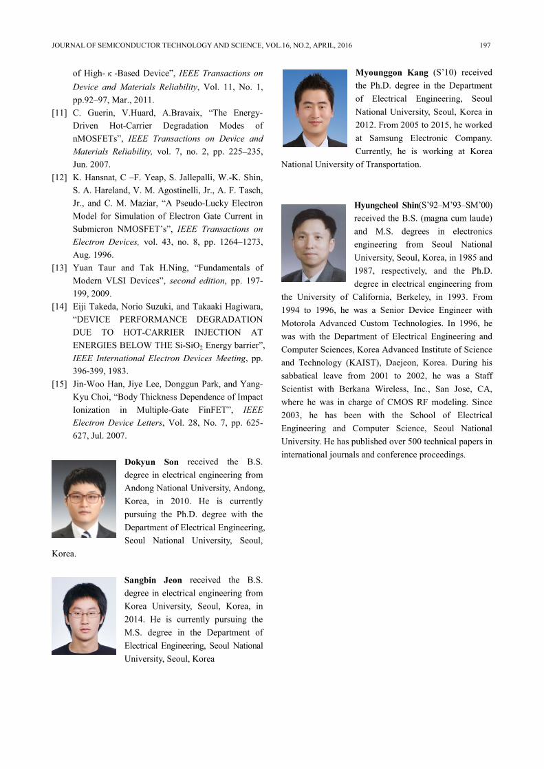
Dokyun Son received the B.S. degree in electrical engineering from Andong National University, Andong, Korea, in 2010. He is currently pursuing the Ph.D. degree with the Department of Electrical Engineering, Seoul National University, Seoul,
Korea.
Sangbin Jeon received the B.S. degree in electrical engineering from Korea University, Seoul, Korea, in 2014. He is currently pursuing the M.S. degree in the Department of Electrical Engineering, Seoul National University, Seoul, Korea
Myounggon Kang (S’10) received the Ph.D. degree in the Department of Electrical Engineering, Seoul National University, Seoul, Korea in 2012. From 2005 to 2015, he worked at Samsung Electronic Company. Currently, he is working at Korea
National University of Transportation.
Hyungcheol Shin(S’92–M’93–SM’00) received the B.S. (magna cum laude) and M.S. degrees in electronics engineering from Seoul National University, Seoul, Korea, in 1985 and 1987, respectively, and the Ph.D. degree in electrical engineering from
the University of California, Berkeley, in 1993. From 1994 to 1996, he was a Senior Device Engineer with Motorola Advanced Custom Technologies. In 1996, he was with the Department of Electrical Engineering and Computer Sciences, Korea Advanced Institute of Science and Technology (KAIST), Daejeon, Korea. During his sabbatical leave from 2001 to 2002, he was a Staff Scientist with Berkana Wireless, Inc., San Jose, CA, where he was in charge of CMOS RF modeling. Since 2003, he has been with the School of Electrical Engineering and Computer Science, Seoul National University. He has published over 500 technical papers in international journals and conference proceedings.