3D Printing for Electronics Manufacturing IEEE CPMT Webinar Mike O’Reilly Aerosol Jet Product Manager
3D Printing for Electronics Manufacturing - IEEEeps.ieee.org/images/files/webinars/webinar93dprintingoreillyfeb... · 3D Printing for Electronics Manufacturing IEEE CPMT Webinar
3D Printing for Electronics ManufacturingIEEE CPMT Webinar
Mike O’ReillyAerosol Jet Product Manager
Presenter
Presentation Notes
Hello and Welcome to the IEEE Webinar on 3D Printed Electronics. My name is Mike O’Reilly and I’ve been with Optomec for ~8 Years. I’ve been in the middle of the printed electronics evolution from lab based tools testing out new design theories to full on manufacturing printing devices on a 24X7 basis. Over the next 30 minutes my goal is to share with you the evolution of 3D Printed Electronics and how it is benefiting mainstream manufactures today.
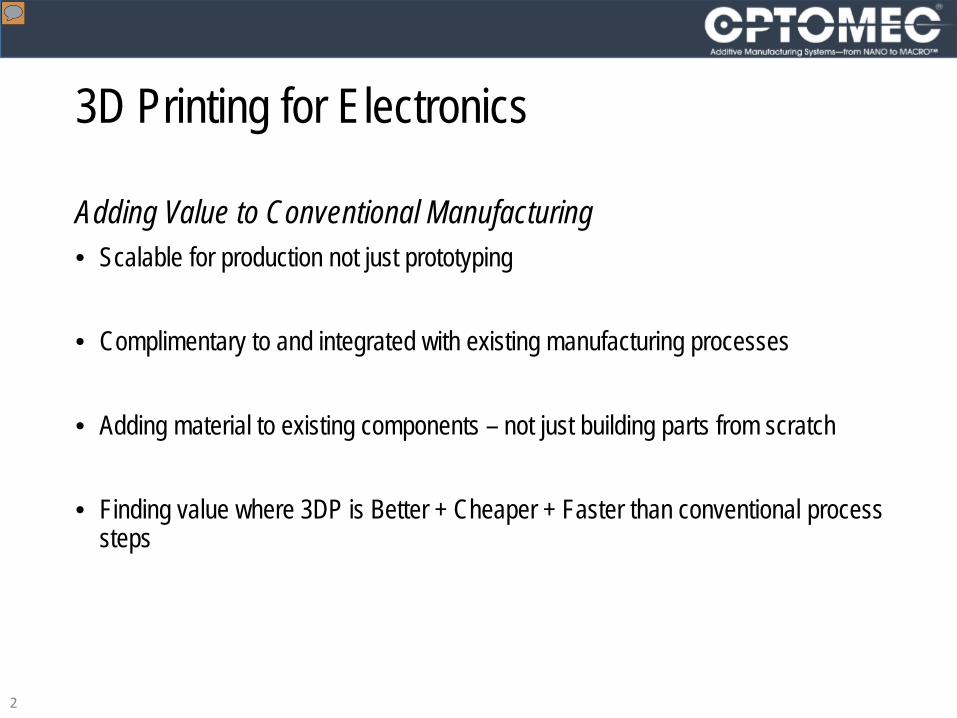
3D Printing for Electronics
Adding Value to Conventional Manufacturing• Scalable for production not just prototyping
• Complimentary to and integrated with existing manufacturing processes
• Adding material to existing components – not just building parts from scratch
• Finding value where 3DP is Better + Cheaper + Faster than conventional process steps
2
Presenter
Presentation Notes
Melba spoke primarily about 3DP as a rapid prototyping, low volume manufacturing solution. However for electronics 3DP provides extended production capabilities that are scalable and complimentary with current manufacturing solutions. 3DPE opens up new avenues in directly functionalizing component parts without the need for plating or costly subtractive manufacturing process steps. 3D Printed Electronics offers unique packaging and functional capabilities not realizable by current manufacturing technologies. We’ll explore some of the areas where 3D printing is currently being deployed and hopefully you will use this presentation as a catalyst in addressing your own design complexity challenges. We will explore how this evolutionary process is benefiting the electronics industry without disrupting current manufacturing processes. And we will review areas where 3DPE is being applied to: Increase product performance and functionality While reducing overall manufacturing costs including the time it takes to manufacturer the physical component
Printed Electronics In Manufacturing
3
Presenter
Presentation Notes
Printed electronics has been around for a very long time. We find it in the majority of electronics manufacturers production lines. Screen printing has a variety of uses in the electronic production line. Masks, both circuit and solder are fond everywhere. Screen Printing is the mainstay of the photovoltaic industry for printing front and rear side energy collector circuits Gravure printing is another technology that is used for RFID tag manufacturing, display circuitry, and other common electronics circuits. Ink Jet and Aerosol Jet are used for a wide variety of manufacturing applications ranging from the printing of sensor circuits and 2D antenna, solid oxide fuels cells, display jumper circuits and edge connectors, and various OLED applications including over printing conductive bus bars to improve current carrying capabilities to depositing emissive materials.
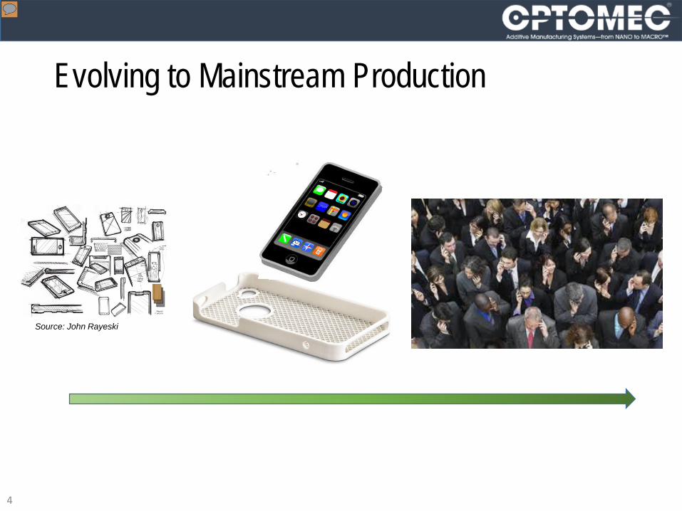
Evolving to Mainstream Production
Source: John Rayeski
4
Presenter
Presentation Notes
OK great. We have demonstrated that 3D printing of electrical circuits works, but how do we scale from the lab or low volume production to the mainstream factory floor. Building a prototype along with a handful of devices to debug is pretty straightforward. Scaling for large volume production opens up new challenges. Can 3DPE meet stringent repeatability requirements? Will it withstand 24X7 operation? Can it achieve throughput requirements to meet customer demands? Will it work with a wide variety of conductive inks and other electronic materials? Will it be too disruptive to my proven manufacturing processes? Will it allow me to achieve expected ROI? 3D PE must meet all of these requirements and more due to adoption cycle concerns and new technology challenges. However, PE is well entrenched and proven production solutions used every day. Extending these proven PE solutions to support 3D applications is just starting to make its way into mainstream production lines.
Printed Electronics offers an attractive, evolutionary alternative to traditional manufacturing solutions. It has the possibility to address increased functionality in reduced packaging formats. It can eliminate costly subtractive process steps and reduce material usage. PE solutions such as Aerosol Jet can be used in the manufacture of both planar and non-planar devices. In the past these devices may have required tens of electronic manufacturing process steps. PE has the potential to streamline from tens to just a few process steps reducing facilities requirements, improving overall product quality, and addressing ever growing environmental challenges.
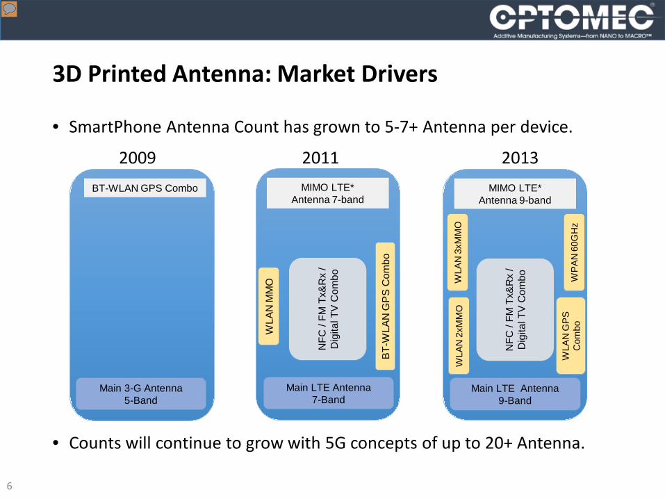
3D Printed Antenna: Market Drivers
• SmartPhone Antenna Count has grown to 5-7+ Antenna per device.
2009 2011 2013
• Counts will continue to grow with 5G concepts of up to 20+ Antenna.
BT-WLAN GPS Combo
Main 3-G Antenna5-Band
MIMO LTE* Antenna 7-band
Main LTE Antenna7-Band
WLA
N M
MO
BT-
WLA
N G
PS
Com
bo
NFC
/ FM
Tx&
Rx
/ D
igita
l TV
Com
bo
MIMO LTE* Antenna 9-band
Main LTE Antenna9-Band
NFC
/ FM
Tx&
Rx
/ D
igita
l TV
Com
boWLA
N 3
xMM
OW
LAN
2xM
MO
WP
AN
60G
Hz
WLA
N G
PS
C
ombo
6
Presenter
Presentation Notes
Today antenna are manufactured as discrete devices and assembled into smartphones, tablets, notebooks, PC’s, etc. Each antenna operates at a specific frequency range. Functional requirements are driving fully embedded antenna be written directly on the smartphone and other smart devices cases. Antenna must be manufactured on this 3D geometry requiring automation solutions capable of having 3, 4, and 5 axis of motion.
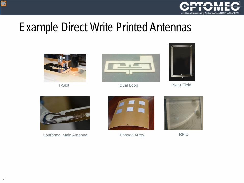
Example Direct Write Printed Antennas
T-Slot Dual Loop Near Field
Phased ArrayConformal Main Antenna RFID
7
Presenter
Presentation Notes
Example 2D and 3D antennas printed with Aerosol Jet multi-axis deposition solutions. Many other types of antenna have been printed, but due to NDA restriction can not be shown.
Competing 3D Antenna Mfg. Technologies
Process 2D Antenna
3D Antenna Digital
Common Plastics
No Plating
Feature Size
Direct Write √ √ √ √ √ < 50 um
LDS Additive √ √ √ 150 um
2 Shot √ √ √ 400 um
Hot Foil √ √ √ 1000 um
Aerosol Jet - DW
LPKF - LDS
Direct Write Advantages• Fewer Steps, Less Floor Space, Simplified Logistics• Standard Plastics, No Additives or Special Coatings• No Plating, No Nickel, Environment Friendly• Projected cost savings as much as 15% or more
compared to LDS’
8
Presenter
Presentation Notes
3D Direct Write Printed Electronics is not the only solution for manufacturing 3D antenna or MID circuits. 3DPE is actually a newcomer to this market. Hot foil has been around for many years. It allows previously 2D manufactured circuits to be applied to 3D surfaces. 2-component injection molding (2-Shot) is used to manufacture MIDs (Molded Interconnect Devices). This method is tied to product-specific tools to create a circuit on the component. The associated high initial manufacturing costs considerably limit the efficiency of this method for small production runs and design modifications. Prototyping shortly before series production is almost impossible. Increasing miniaturization of the circuits on MID components leads to a considerable rise in tooling-up time and expense. Laser Direct Structuring (LDS) works with doped thermoplastics delivered as an injection molded part. The laser-activated thermoplastic is doped with a special additive. It is activated by a laser. A physical-chemical reaction forms metallic nuclei. These act as a catalyst for reductive copper plating. In addition to activation, the laser creates a microscopically rough surface in which the copper is firmly anchored during metallization. Aerosol Jet prints directly on the surface of an injection molded part which was constructed out of standard material such as polycarbonate. Once the pattern has been printed with a conductive ink, typically Ag, it is then fully cured in an oven to meet both mechanical and electrical requirements. The components are now ready for assembly.
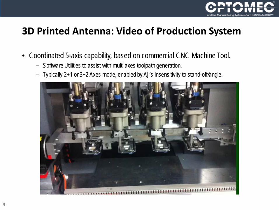
3D Printed Antenna: Video of Production System
• Coordinated 5-axis capability, based on commercial CNC Machine Tool.‒ Software Utilities to assist with multi axes toolpath generation.‒ Typically 2+1 or 3+2 Axes mode, enabled by AJ’s insensitivity to stand-off/angle.
9
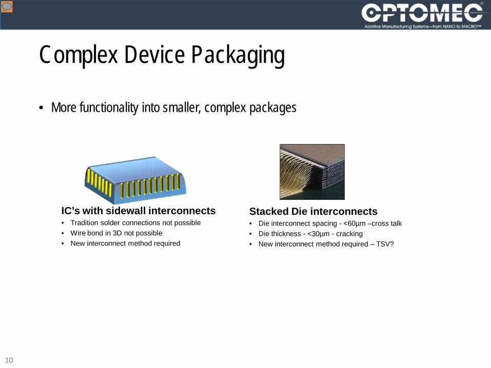
Complex Device Packaging
• More functionality into smaller, complex packages
IC’s with sidewall interconnects• Tradition solder connections not possible• Wire bond in 3D not possible• New interconnect method required
Stacked Die interconnects• Die interconnect spacing - <60µm –cross talk • Die thickness - <30µm - cracking• New interconnect method required – TSV?
10
Presenter
Presentation Notes
Referring back to the Smart Device Core Components slide, 3D Direct Write techniques may play a critical role in next generation electronic packaging Stacking multiple dies into a small semiconductor package is pushing the limits of what traditional manufacturing technology is capable of. New, evolutionary manufacturing solutions are required and printed electronics is poised to augment those manufacturing gaps.
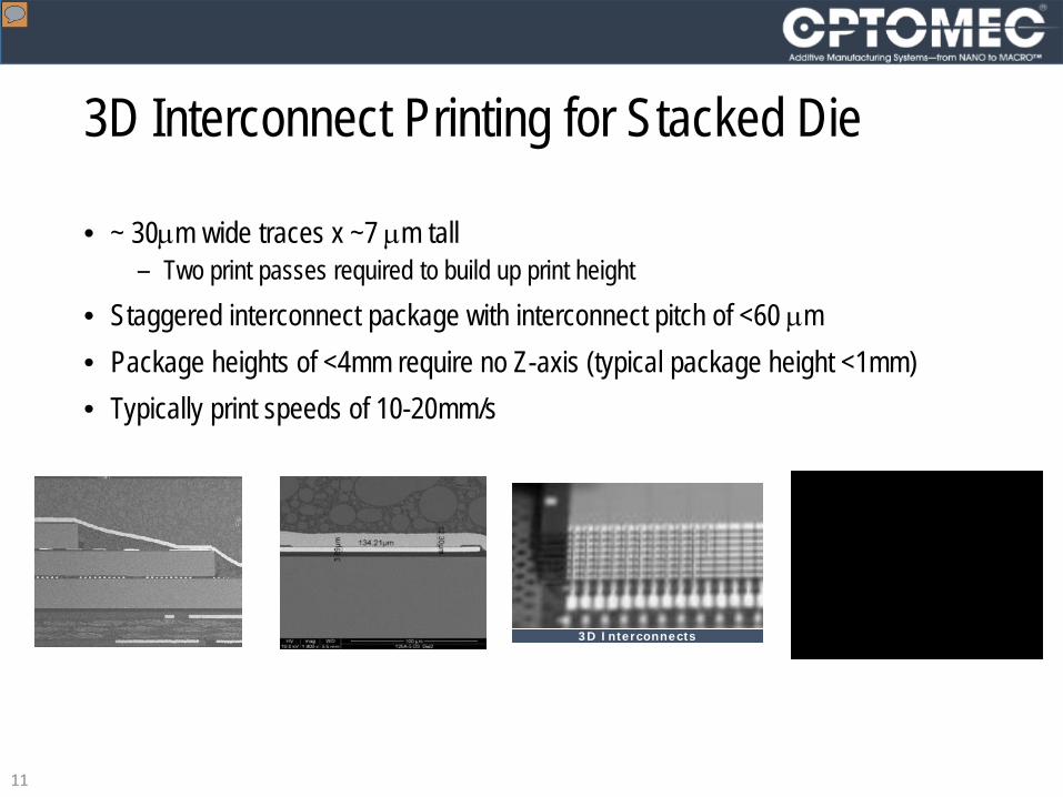
3D Interconnect Printing for Stacked Die
• ~ 30µm wide traces x ~7 µm tall‒ Two print passes required to build up print height
• Staggered interconnect package with interconnect pitch of <60 µm• Package heights of <4mm require no Z-axis (typical package height <1mm)• Typically print speeds of 10-20mm/s
3D Interconnects
11
Presenter
Presentation Notes
Aerosol Jet’s ability to print fine traces over complex surfaces provides a viable alternative to traditional wire bond and emerging TSV manufacturing solutions. With traces <30 microns and pitches <50 microns new manufacturing methods need to be found that address continuing package challenges. At 60 micron spacing wire bond technology is susceptible to wire sway creating cross talk between signals. For multiple stacked die from multiple vendors, the lack of interchangeable TSV formats limits which die can be stacked together. This coupled with increasing manufacturing complexity makes TSV a challenging solution to move to.
Direct Write’s Fit within the 3DIC Value Chain
+ 80,000 Wire Bonders+ 20 um wires/ 35 um pitch+ Fast/Accurate/Cost Effective- impedance/cross talk/micro
crack on thin die/
Incumbent Process
20152010
+ 50 TSV Research Org+ Sensors/MEMS/amps in prod.+ Best for elec. performance- Time/Cost/Yield
Emerging ProcessDirect Write 3D
Process+ fine line/fine pitch + non-contact + shorter interconnects
Bottom Line:• Device manufacturers may need fast track path to market• Device manufacturers may need flexible methods to introduce new technology• DW can fill the gap between WB and TSV to meet high performance time to market requirements
12
Presenter
Presentation Notes
Direct Write offers an alternative to both Wirebond and TSV packaging challenges. It enables an evolutionary path between traditional packaging techniques as new standards emerge and fills a much need solutions gap between the old and new solutions.
Functionalized 3D Plastic Parts: Aerospace
• Joint Project with Aurora Flight Sciences & Stratasys‒ Fully Printed Wing Structure & Electronics‒ FDM Process Prints Wing using Aerospace Grade Material‒ Process Prints Sensor, RF Antenna and Power Circuits on Wing‒ Demonstrated at DMC Conference
• Advantages‒ Lighter Weight, Higher Performance ‒ Conformal Electronics, More Payload‒ Fully Functional RP & RM ‒ Simplified Electro-Mechanical Integration‒ Point of Use Repair + Reconfiguration
13
Presenter
Presentation Notes
Another example of a functionalized model was a joint UAV project between Stratasys, Aurora flight sciences, manufacturer of UAVs, and Optomec. The UAV structure was printed with a Fortus FDM system. The electronics, including power and signal circuits, high band RF antenna, and strain gauge were printed with Optomec’s Aerosol Jet. The advantages of printing the UAV – simplified micro-electronic assembly, point of use repair, manufacturing, and reconfiguration.
Printed Signal & Power Circuit
• Printed circuit in <30 minutes• CTE miss-match cracked circuits during sintering process, but were easily repaired• Signal Circuit
‒ <30Ω‒ Lit surface mounted LED
• Power Circuit‒ <1Ω‒ Powered a motor at 0.5 amps @ 20 volts
14
Presenter
Presentation Notes
All of the FDM printed components took ~10 hours to print. The power and signal circuits were both printed in ~ 30 minutes. We ran into some issues with the CTE (Coefficient of Thermal Expansion) mismatch between the Ag and the ULTEM. ULTEM9085’s CTE is around 4x10 to the -5 while Ag is a nearly an order of magnitude lower. The material did crack, however, we were able to repair it. The signal circuit lite the LED at the end of the wing and had less than 30 Ohms resistance The power circuit showed less than one Ohm resistance and powered the motor at 0.5 amps @ 20 Volts
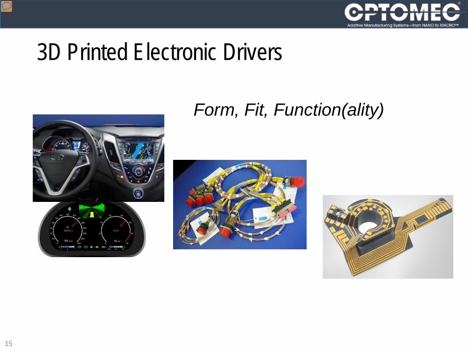
3D Printed Electronic Drivers
Form, Fit, Function(ality)
15
Presenter
Presentation Notes
As you’ve already heard, 3D parts are playing a major role in rapid prototyping new products and in the manufacture of low volume parts and components. 3D printed electronics is playing an ever increasing role in mainstream electronics as consumer driven requirements continue to push requirements for more functionality, but confined within an already cramped product envelop. Consider the operators “console” in the latest automobiles. Digital displays for accurate, instantaneous operator feedback Dynamic feedback regarding your cars performance and operational readiness Voice activated look-ahead warning systems Fully integrated navigation and audio systems Rear and side view mirror feedback systems All of which must fit in an ergonomic form and seamlessly integrate with each other. This is driving new levels of component, sub-system, and system integration where traditional manufacturing solutions are becoming problematic. New capabilities such as Molded Interconnect Devices (MIDs) containing electrical interconnect circuits that tie all of these various components and systems together are rapidly gaining traction in mainstream manufacturing.
Reliability Standards
Look-Ahead Systems• Must remain clear during winter driving • Clear polycarbonate• Low temperature curing - <120⁰C• Distribute enough thermal energy to defrost snow and ice
16
Presenter
Presentation Notes
With new functions there are new manufacturing challenges. Addressing these challenges require the resources of engineers, material vendors, safety personnel, and the passing of a wide range of environmental tests. Designing a new circuit with the appropriate energy to remove ice and snow from critical “keep clean” areas to ensure sensing equipment remains operational may seem straight forward. But consider that your heater circuit may melt the plastic it was printed on. Key considerations need to be addressed: Substrate type and thermal melting points Conductive material type; sintering temperature; electrical performance (resistance); adhesion; and other performance details Circuit deposition process Manufacturing throughput and uptime requirements Overall ROI Let’s look at the practical application of 3D Printed Electronics in the following examples
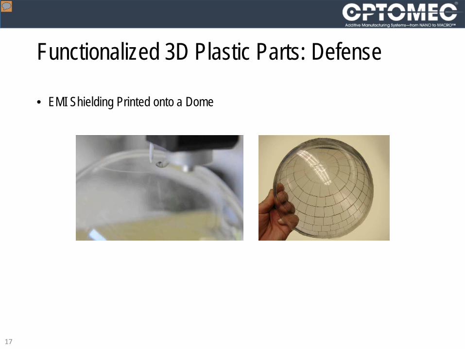
Functionalized 3D Plastic Parts: Defense
• EMI Shielding Printed onto a Dome
17
Presenter
Presentation Notes
This example shows the integration of Printed Electronics on 3D Structures….Aerosol Jet was used to print shielding against electro magnetic interference on a plastic dome. One approach to create electronics onto 3D shapes is to use 2D manufacturing techniques. For example, electronic circuits can be produced on a 2D flexible substrate and then molded around a 3D surface. This approach works for surfaces such as cylinders that can be projected onto a planner 2D surfaces, but it doesn’t work for shapes such as hemispheres.
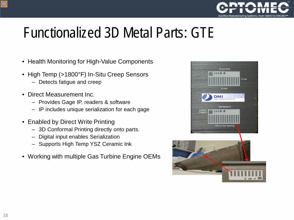
Functionalized 3D Metal Parts: GTE
• Health Monitoring for High-Value Components
• High Temp (>1800°F) In-Situ Creep Sensors‒ Detects fatigue and creep
• Direct Measurement Inc. ‒ Provides Gage IP, readers & software‒ IP includes unique serialization for each gage
• Enabled by Direct Write Printing‒ 3D Conformal Printing directly onto parts.‒ Digital input enables Serialization‒ Supports High Temp YSZ Ceramic Ink
• Working with multiple Gas Turbine Engine OEMs
18
Presenter
Presentation Notes
Gas Turbine Engine example – Aerosol Jet was used to print creep sensors on titanium blades using high temperature ceramic ink Yittria Stabilized Zerconia…..printed directly on the surface…providing in-situ monitoring for blade expansion. Each sensor is individually serialized during the printing process to provide unique identification for each gage. Other methods such as printing a decal and affixing it onto the blade or laser scribing failed. The decal did not standup to the operating environment, >800F, and the laser scribe couldn’t provide sufficient contrast for optical scanning.
PE Challenges
Meeting Manufacturing Requirements
• Material Supply‒ Volume nanoparticle manufacturers
• Mechanical Properties‒ Adhesion‒ Corrosion‒ General duration
• Electrical‒ Meeting performance objectives‒ On various substrates
• Environmental standards‒ Meeting Hast/Bhast, High/Low Accelerated tests, Shock tests and other required manufacturing
standards• Process Development
‒ 2, 3, 5 Axis toolpath generation‒ Matching material to substrates
• Safety Standards‒ OSHA, IPC, EU standards just emerging
20
Presenter
Presentation Notes
There is lots to be done for 3DPE to take hold on the mainstream production floor, but rapid headways is taking place. Manufacturing drivers remain in place with the key being ROI. Ensuring that the all of the elements required in the manufacturing process are in place including substrates, inks, deposition processes, compliance tests, and other key items will require diligence on the part of everyone involved in the supply chain.
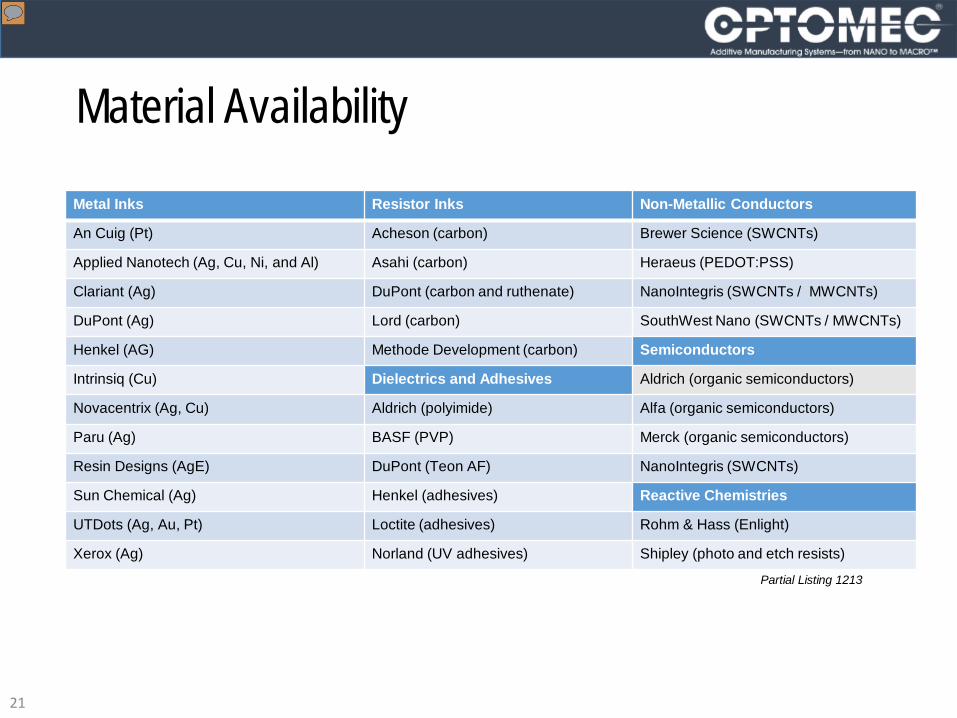
Material Availability
Metal Inks Resistor Inks Non-Metallic Conductors
An Cuig (Pt) Acheson (carbon) Brewer Science (SWCNTs)
Xerox (Ag) Norland (UV adhesives) Shipley (photo and etch resists)
Partial Listing 1213
21
Presenter
Presentation Notes
Key electronic material vendors are committed to meeting volume requirements being dictated by early 3DPE manufacturing adopters. All are working closely with Optomec and it’s customers to meet evolving performance and sintering temperature demands in an ever changing economic climate.
3D Printing for Electronics
3D Printing – Adding Value to Conventional Manufacturing• Scalable for production not just prototyping
• Complimentary to and integrated with existing manufacturing processes
• Adding material to existing components – not just building parts from scratch
• Finding value where 3DP is Better+Cheaper+Faster than conventional process steps
22
Presenter
Presentation Notes
We’ve explored how 3DP for electronics provides extended production capabilities that are scalable and complimentary with current manufacturing solutions. We’ve demonstrated how 3DPE opens up new avenues in directly functionalizing component parts without the need for plating or costly subtractive manufacturing process steps. We’ve explored some of the areas where 3DPE is successfully being deployed as complementary solutions to existing manufacturing processes with key benefits of Increased product performance and functionality And reduced overall manufacturing costs including the time it takes to manufacturer the physical component. 3D Electronics is real, it’s here, and it’s being deployed to meet the ever changing requirements of a new generation of electronic products.
Thank YouFor More Information on Aerosol Jet Products Contact: