Embed Size (px)
Citation preview

Tezzaron Semiconductor 02/07/2012
3D Integration:
New Opportunities for Speed,
Power and Performance
Robert Patti, CTO
1

Tezzaron Semiconductor 02/07/2012
Why We Scale?
2
>180nm 90nm 65nm 130nm 45nm 28nm 22nm 16nm
Cost
Speed
Power
Size
What can 3D do for us?
Ad
van
tag
es

Tezzaron Semiconductor 02/07/2012
3D Stacking Approaches
Irvine Sensors : Stacked Flash
Amkor : 4S CSP (MCP)
Chip Level Device Level Wafer Level
Matrix: Vertical TFT
• Infineon/IBM
• RPI
• ZyCube
Tezzaron
• Ziptronix
• Xan3D
• Vertical Circuits
Samsung : Stacked Flash
• Stanford
• Besang
Tezzaron Semiconductor 02/07/2012
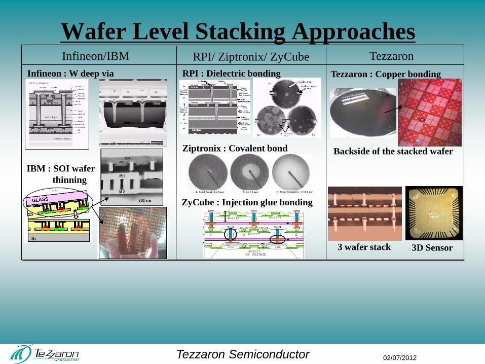
Wafer Level Stacking Approaches Infineon/IBM RPI/ Ziptronix/ ZyCube Tezzaron
3 wafer stack
Ziptronix : Covalent bond
IBM : SOI wafer
thinning
Backside of the stacked wafer
Infineon : W deep via RPI : Dielectric bonding
ZyCube : Injection glue bonding
Tezzaron : Copper bonding
3D Sensor

Tezzaron Semiconductor 02/07/2012
Market Drivers: 3D
Driver Functionality Technical
Parameter # 1
Technical
Parameter # 2
Value Indicator
Stacked
NAND Flash
Cell Phones
Hard Drives
Flash Drives
Memory density High packing
density
Micro-
processor +
Memory
Workstations Latency
bandwidth
Power Execution time
Memory Multiple Density Latency Varies
Image
Sensor
Cell Phones
Cameras
Automotive
Quantum
Efficiency
Number of pixels Image Quality

Tezzaron Semiconductor 02/07/2012
There is a lot of 3D today
4 die 65nm interposer
560μ
16Gb NAND flash (2Gx8 chips),
Wide Bus DRAM
Xilinx
Samsung
Micron
RF Silicon Circuit Board / TSV
Logic & Analog
IBM
3D NAND Toshiba
Wide Bus DRAM
Intel CPU + memory
CMOS Sensor OKI
PIN Detector Device Raytheon/Ziptronix
6

Tezzaron Semiconductor 02/07/2012
Through-Silicon Via (TSV)
• Via First
• Via Last
• Via at Front end (FEOL)
• Via at Mid line (MOL?)
• Via at Back end (BEOL)
“SuperContact”
Dr. J.Q. Lu
RPI

Tezzaron Semiconductor 02/07/2012
Span of 3D Integration
CMOS 3D CMOS 3D
Analog
Flash
DRAM
DRAM
CPU
Analog
Flash
DRAM
DRAM
CPU
3D Through Via Chip Stack
100,000,000s/sqmm Transistor to Transistor
Ultimate goal
1s/sqmm Peripheral I/O
Flash, DRAM
CMOS Sensors
3D-ICs 100-1,000,000/sqmm
1000-10M Interconnects/device
Packaging Wafer Fab
IBM IBM/Samsung
8

Tezzaron Semiconductor 02/07/2012
3D Interconnect Characteristics
SuperContactTM
I
200mm
Via First, FEOL
SuperContactTM
III
200mm
Via First, FEOL
SuperContactTM
IV
200mm
Via First, FEOL
Interposer
TSV
Bond Points Die to
Wafer
Size
L X W X D
Material
1.2 X 1.2
X 6.0
W in Bulk
0.85 X 0.85
X 10
W in Bulk
0.60 X 0.60
X 2
W in SOI
10 X 10
X 100
Cu
1.7 X 1.7
Cu
3 X 3
Cu
Minimum
Pitch
<2.5 1.75 0.8 30/120 2.4 5
Feedthrough
Capacitance
2-3fF 3fF 0.2fF 250fF << <25fF
Series
Resistance
<1.5 W <3 W <1.5 W <0.5 W < <
9

Tezzaron Semiconductor 02/07/2012
10um TSV
20um Pitch
TSV Pitch ≠ Area ÷ Number of TSVs • TSV pitch issue example
– 1024 bit busses require a lot of space with larger TSVs
– They connect to the heart and most dense area of processing
elements
– The 45nm bus pitch is ~100nm; TSV pitch is >100x greater
– The big TSV pitch means TOF errors and at least 3 repeater
stages
F
P
U
1024 bit bus
Single layer
interconnect
1um TSV
2um Pitch
10

Tezzaron Semiconductor 02/07/2012
A Closer Look at Wafer-Level Stacking
Dielectric(SiO2/SiN)
Gate Poly
STI (Shallow Trench Isolation)
Oxide
Silicon
W (Tungsten contact & via)
Al (M1 – M5)
Cu (M6, Top Metal)
“Super-Contact”
11

Tezzaron Semiconductor 02/07/2012
Next, Stack a Second Wafer & Thin:
12

Tezzaron Semiconductor 02/07/2012
Two wafer Align & Bond Course Grinded Fine Grinded
After CMP Si Recessed
Stacking Process Sequential Picture
Misalign=0.3um
Top wafer
Bottom wafer
High Precision Alignment
13

Tezzaron Semiconductor 02/07/2012
3rd wafer 2nd wafer 1st wafer: controller
Then, Stack a Third Wafer:
14

Tezzaron Semiconductor 02/07/2012
1st wafer: controller 2nd wafer 3rd wafer
Finally, Flip, Thin & Pad Out:
This is the
completed stack!
15

Tezzaron Semiconductor 02/07/2012
3rd Si thinned to 5.5um
2nd Si thinned to 5.5um
1st Si bottom supporting wafer
SiO2
16

Tezzaron Semiconductor 02/07/2012 17
TSVs

Tezzaron Semiconductor 02/07/2012 18

Tezzaron Semiconductor 02/07/2012
DRAM wants 2 different processes!
Bit cells Low leakage
-slow refresh
-low power
-low GIDL
High Vt Devices
Vneg Well
Thick Oxide
Sense Amps
Word line drivers
Device I/O
High speed
-better sensitivity
-better bandwidth
-lower voltage
Low Vt Devices
Copper interconnect
Thin Oxides

Tezzaron Semiconductor 02/07/2012
“Dis-Integrated” 3D Memory
Wordline Drivers
Senseamps
Memory
Cells
I/O Drivers
Memory
Layers
Controller
Layer
Bitlines Wordlines
Power,Ground,
VBB,VDH
20

Tezzaron Semiconductor 02/07/2012
Octopus Stack
21
DRAM Control/Logic DRAM Memory Cells
2 Layer Stacked Device
(SEM)

Tezzaron Semiconductor 02/07/2012
Octopus DRAM
• 1-4Gb
• 16 Ports x 128bits (each way)
• @1GHz – CWL=0 CRL=2 SDR format
– 5ns closed page access to first data (aligned)
– 12ns full cycle memory time
– 288GB/s data transfer rate
• Max clk=1.6GHz
• Internally ECC protected, Dynamic self-repair, Post attach repair
• 115C die full function operating temperature
• JTAG/Mailbox test&configuration
• Power -40%
• Density x4++
• Performance +300%
• Cost -50%
22

Tezzaron Semiconductor 02/07/2012
Main Memory Power Cliff
DDR3 ~40mW per pin
1024 Data pins →40W
4096 Data pins →160W
Die on Wafer ~24uW per pin

Tezzaron Semiconductor 02/07/2012
The Industry Issue
1
10
100
1000
10000
Best Case Number of channels to support Float OPS
Worst Case Number of channels to support Float OPS
Best Case Number of channels to support OPS
Worst Case Number of channels to support OPS
Best Case Number of channels to support mixed OPS
DD
R2
/3/4
Mem
ory
Ch
ann
els
To continue to increase CPU
performance, exponential
bandwidth growth required.
More than 200 CPU cycles of
delay to memory results in cycle
for cycle CPU stalls.
16 to 64 Mbytes per thread
required to hide CPU memory
system accesses.
No current extension of existing
IC technology can address
requirements.
Memory I/O power is running
away.
Need 50x bandwidth improvement.
Need 10x better cost model than embedded
memory.
24

Tezzaron Semiconductor 02/07/2012
The “Killer” App: Split-Die Embedded Performance with far
superior cost/density.
110nm DRAM node has better
density than 45nm embedded
DRAM.
1000x reduction in I/O power.
I/O Pad area : Bumping or wire bonding
Customer Host Device
DRAM
Tezzaron 3D DRAM
25

Tezzaron Semiconductor 02/07/2012
Die to Wafer With BCB Template
•KGD
•2um alignment / 5um pitch limit
•Cu-Cu thermo compression bonding
•Multilayer capability
RPI Effort
under Dr.
James Lu
26

Tezzaron Semiconductor 02/07/2012
Logic on Memory
172 pads 92 pads
(528 total pads at edge, stagger
250um pad, 125um pitch
~1500 available pads)
199 I/O
Bondpoints/side
8 DRAM ports
16x21 pad array
>10f bypass caps
SS ~4,000pf 27
Memory also
acts as
interposer
Memory
Logic

Tezzaron Semiconductor 02/07/2012
Hyper-Integration
5-9 layer stacks
Layer 5 Layer 7 Layer 9 Layer
Poly 9 11 17
Copper Wire 21 (25) 32 (38) 34 (42)
Al/W Wire 7 7 13
Trans. Count 3B 3.1B 5.5B
2-4 layer
logic device
Face to Face
Bond
5x5 mm
Octopus
memory
device
21.8x12.3 mm
(2 -5 layer)
Bond pads
528 available
Stagger
125um pitch
Controller
Memory
Memory TSVs
28

Tezzaron Semiconductor 02/07/2012
DRAM Die
“extra TSVs”
~40,000 in the core area
~250,000 on periphery
“extra TSVs”
~100,000 in the core area
~50,000 in gap
Customer circuits

Tezzaron Semiconductor 02/07/2012
Current Memory Split-Die Projects
Memory Die
C64 Processor
Flip-Chip Solder Balls

Tezzaron Semiconductor 02/07/2012
R8051/Memory
5X Performance 1/10th Power
31

Tezzaron Semiconductor 02/07/2012 32

Tezzaron Semiconductor 02/07/2012
Tezzaron 3D
Devices June/July
2011
33

Tezzaron Semiconductor 02/07/2012
2.5/3D Circuits
34
CC
FPGA (4Xnm)
Active Silicon Circuit Board
2 Layer Processor2 Layer Processor3 Layer 3D Memory
CC
Organic Substrate
level#0
level#1
level#2
level#3
Solder Bumps
μBumps
C4 Bumps
Die to Wafer Cu Thermal Diffusion Bond
level#4

Tezzaron Semiconductor 02/07/2012
3D MPW
• Complete 3D PDK 8th Release – GF 130nm
– Calibre, Synopsis, Hspice, Cadence
– MicroMagic 3D physical editor
– Magma 3D DRC/LVS
– Artisan standard cell libraries
• MOSIS, CMP, and CMC MPW support – 90nm, 150nm SOI
– Silicon Workbench
• >70 in process
• >400 users
35

Tezzaron Semiconductor 02/07/2012
Near End-of-Line
poly
STI
SIN M1
M2
M3
M4
M5
M6
M7
5.6µ TSV is 1.2µ
Wide and ~10µ deep
W
M8
TM
M4
M5
2x,4x,8x Wiring level
~.2/.2um S/W
36

Tezzaron Semiconductor 02/07/2012
New Apps – New Architectures
37

Tezzaron Semiconductor 02/07/2012
Relative TSV Size
38

Tezzaron Semiconductor 02/07/2012
Pitch and Interconnect
• SuperContactTM is 500f 2 (including spacing)
• Face to face is 350f 2 (including spacing)
• Chip on wafer I/O pitch is 35,000f 2
• Standard cell gate is 200 to 1000f 2
– 3 connections
• Standard cell flip-flop is 5000f 2
– 5 connections
• 16 bit sync-counter is 125,000f 2
– 20 connections
• Opamp is 300,000f 2
– 4 connections
39
f 2 is minimum feature
squared

Tezzaron Semiconductor 02/07/2012
The Applications
• Sensors
– CMOS cameras
– POI image processors – very high frame rates
– High Energy Physics
• Bio Assay
– SOC++
• Logic Memory
• Logic - Logic
40

Tezzaron Semiconductor 02/07/2012
OC768 Packet Engine
Dual PPC 64x ARM SOC
FPGA (CPU Augmentation)
DRAM
Flash
CAM
CAM
FPGA (Packet Cracker)
Stack Controller

Tezzaron Semiconductor 02/07/2012
TBUS
EAST
WEST
NORTH
SOUTH
3D-Routing Node (NOC)
UP
DOWN

Tezzaron Semiconductor 02/07/2012
Fault Tolerant
Self-configuring/Re-configuring
Stack Manager
Processor0
TBS
TBU
routing nodes tbus
tbus
Stack Manager
Processor1
TBS
TBU
routing nodes tbus
tbus
TBC
TBC
tbus
tbus

Tezzaron Semiconductor 02/07/2012
3D Interconnect

Tezzaron Semiconductor 02/07/2012
3D Interconnect

Tezzaron Semiconductor 02/07/2012
Data Paths: On-ramp/Off-ramp
Slab N
Slab N+1
Clock, Data, Frame
Clock, Data, Frame
3D-Routing
Node
3D-Routing
Node

Tezzaron Semiconductor 02/07/2012
130nm Implemented Node

Tezzaron Semiconductor 02/07/2012
DRC, LVS, Transistor
synthesis, Crossprobing.
Multiple tapeouts,
0.35um-45nm
>20GB, ~10B devices
Independent tech files for each tier.
Saves GDSII as flipped or rotated.
Custom output streams for 3D DRC / LVS.
MAX-3D by Micro Magic, Inc.
Fully functional 3D layout editor.
48

Tezzaron Semiconductor 02/07/2012
3D Place & Route
49

Tezzaron Semiconductor 02/07/2012
3D LVS using QuartzLVS from Magma
• Key features – LVS each of the 2D designs as well as the 3D
interconnections between them in a single run
– Driven by a 3D “tech file” that specifies the number and
order of layers, interconnect material, etc
– TSV aware LVS extraction
– Full debug environment to analyze any LVS mismatch
# 3D LVS Tech file WAFER: 1
LAYOUT TOP BLOCK: lvslayer1_1
SCHEMATIC TOP BLOCK: lvslayer1
GDSII FILE: lvslayer1_1.gds
SCHEMATIC NETLIST: lvslayer1.sp
INTERFACE UP METAL: 1;0
INTERFACE UP TEXT: 1;101
...
INTERFACE:
LAYOUT TOP BLOCK: lvstop
SCHEMATIC TOP BLOCK: lvstop
GDSII FILE: lvstop_ALL.gds
SCHEMATIC NETLIST: lvstop.sp
BOND OUT METAL: 5;0
BOND OUT TEXT: 5;101
50

Tezzaron Semiconductor 02/07/2012
Challenges
• Tools
– Partitioning tools
– 3D P&R
• Access
• Heat
• Testing
– IEEE 1500
– IEEE 1149
• Standards
– Die level
• JEDEC JC-11 Wide bus memory
– Foundry interface
51

Tezzaron Semiconductor 02/07/2012
Summary
• 3D has numerous and vast opportunities!!
– New design approaches
– New ways of thinking
– Best of class integration of
• Memory
• Logic
• RF
• MEMS
52
Sensors
Computing
MEMS
Communications