Embed Size (px)
Citation preview
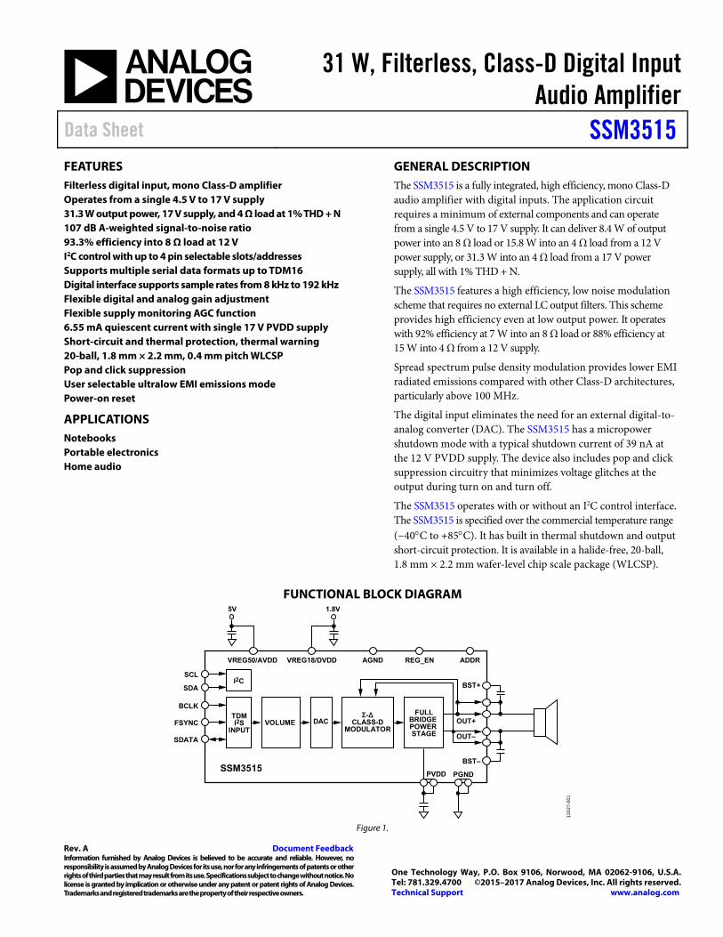
31 W, Filterless, Class-D Digital Input Audio Amplifier
Data Sheet SSM3515
Rev. A Document Feedback Information furnished by Analog Devices is believed to be accurate and reliable. However, no responsibility is assumed by Analog Devices for its use, nor for any infringements of patents or other rights of third parties that may result from its use. Specifications subject to change without notice. No license is granted by implication or otherwise under any patent or patent rights of Analog Devices. Trademarks and registered trademarks are the property of their respective owners.
One Technology Way, P.O. Box 9106, Norwood, MA 02062-9106, U.S.A.Tel: 781.329.4700 ©2015–2017 Analog Devices, Inc. All rights reserved. Technical Support www.analog.com
FEATURES Filterless digital input, mono Class-D amplifier Operates from a single 4.5 V to 17 V supply 31.3 W output power, 17 V supply, and 4 Ω load at 1% THD + N 107 dB A-weighted signal-to-noise ratio 93.3% efficiency into 8 Ω load at 12 V I2C control with up to 4 pin selectable slots/addresses Supports multiple serial data formats up to TDM16 Digital interface supports sample rates from 8 kHz to 192 kHz Flexible digital and analog gain adjustment Flexible supply monitoring AGC function 6.55 mA quiescent current with single 17 V PVDD supply Short-circuit and thermal protection, thermal warning 20-ball, 1.8 mm × 2.2 mm, 0.4 mm pitch WLCSP Pop and click suppression User selectable ultralow EMI emissions mode Power-on reset
APPLICATIONS Notebooks Portable electronics Home audio
GENERAL DESCRIPTION The SSM3515 is a fully integrated, high efficiency, mono Class-D audio amplifier with digital inputs. The application circuit requires a minimum of external components and can operate from a single 4.5 V to 17 V supply. It can deliver 8.4 W of output power into an 8 Ω load or 15.8 W into an 4 Ω load from a 12 V power supply, or 31.3 W into an 4 Ω load from a 17 V power supply, all with 1% THD + N.
The SSM3515 features a high efficiency, low noise modulation scheme that requires no external LC output filters. This scheme provides high efficiency even at low output power. It operates with 92% efficiency at 7 W into an 8 Ω load or 88% efficiency at 15 W into 4 Ω from a 12 V supply.
Spread spectrum pulse density modulation provides lower EMI radiated emissions compared with other Class-D architectures, particularly above 100 MHz.
The digital input eliminates the need for an external digital-to-analog converter (DAC). The SSM3515 has a micropower shutdown mode with a typical shutdown current of 39 nA at the 12 V PVDD supply. The device also includes pop and click suppression circuitry that minimizes voltage glitches at the output during turn on and turn off.
The SSM3515 operates with or without an I2C control interface. The SSM3515 is specified over the commercial temperature range (−40C to +85C). It has built in thermal shutdown and output short-circuit protection. It is available in a halide-free, 20-ball, 1.8 mm × 2.2 mm wafer-level chip scale package (WLCSP).
FUNCTIONAL BLOCK DIAGRAM
BCLK
FSYNC
SDATA
OUT+
OUT–
VREG50/AVDD
5V
VREG18/DVDD AGND REG_EN
PVDD PGND
SCL
SDA
ADDR
I2C
TDMI2S
INPUTVOLUME DAC
FULLBRIDGEPOWERSTAGE
Σ-∆CLASS-D
MODULATOR
BST–
BST+
SSM3515
1.8V
1332
7-00
1
Figure 1.

SSM3515 Data Sheet
Rev. A| Page 2 of 41
TABLE OF CONTENTS Features .............................................................................................. 1
Applications ....................................................................................... 1
General Description ......................................................................... 1
Functional Block Diagram .............................................................. 1
Revision History ............................................................................... 2
Specifications ..................................................................................... 3
Digital Timing Characteristics ................................................... 6
Absolute Maximum Ratings ............................................................ 8
Thermal Resistance ...................................................................... 8
ESD Caution .................................................................................. 8
Pin Configuration and Function Descriptions ............................. 9
Typical Performance Characteristics ........................................... 10
Theory of Operation ...................................................................... 19
Overview ...................................................................................... 19
Power Supplies ............................................................................ 19
Power-Up Sequence ................................................................... 19
Power-Down Operation ............................................................ 19
REG_EN Pin Setup and Control .............................................. 19
ADDR Pin Setup and Control .................................................. 20
Clocking ....................................................................................... 20
Digital Audio Serial Interface ....................................................... 21
Stereo (I2S/Left Justified) Operating Mode ............................. 21
TDM Operating Mode ............................................................... 21
I2C Control .................................................................................. 21
Analog and Digital Gain ............................................................ 24
Pop and Click Suppression ........................................................ 24
EMI Noise .................................................................................... 24
Output Modulation Description .............................................. 24
Faults and Limiter Status Reporting ........................................ 25
VBAT Sensing ............................................................................. 25
Limiter and Battery Tracking Threshold Control .................. 25
Layout .......................................................................................... 28
Bootstrap Capacitors.................................................................. 28
Power Supply Decoupling ......................................................... 28
Register Summary .......................................................................... 29
Register Details ............................................................................... 30
Power Control Register ............................................................. 30
Gain and Edge Control Register............................................... 30
DAC Control Register ................................................................ 31
DAC Volume Control Register ................................................. 32
SAI Control 1 Register ............................................................... 33
SAI Control 2 Register ............................................................... 34
Battery Voltage Output Register ............................................... 35
Limiter Control 1 Register ........................................................ 35
Limiter Control 2 Register ........................................................ 36
Limiter Control 3 Register ........................................................ 37
Status Register ............................................................................. 37
Fault Control Register ................................................................ 38
Typical Application Circuit ........................................................... 40
Outline Dimensions ....................................................................... 41
Ordering Guide .......................................................................... 41
REVISION HISTORY1/2017—Rev. 0 to Rev. A Changes to Figure 2 and Table 5 ..................................................... 6 6/2015—Revision 0: Initial Version

Data Sheet SSM3515
Rev. A| Page 3 of 41
SPECIFICATIONS PVDD = 12 V, VREG50/AVDD = 5 V (internal), VREG18/DVDD = 1.8 V (external), RL = 8 Ω + 33 μH, BCLK = 3.072 MHz and FSYNC = 48 kHz, TA = −40°C to +85°C, unless otherwise noted. The measurements are with a 20 kHz AES17 low-pass filter. The other load impedances used are 4 Ω + 15 μH and 3 Ω +10 μH. Measurements are with a 20 kHz AES17 low-pass filter, unless otherwise noted.
The sine wave output powers above 20 W in 4 Ω cannot be continuous and may invoke the thermal limit indicator based on the power dissipation capability of the board.
Table 1. Parameter Symbol Test Conditions/Comments Min Typ Max Unit
DEVICE CHARACTERISTICS Output Power/Channel POUT f = 1 kHz
RL = 8 Ω THD + N = 1%, PVDD = 17 V 16 W THD + N = 1%, PVDD = 12 V 8.4 W
THD + N = 1%, PVDD = 7 V 2.8 W THD + N = 1%, PVDD = 5 V 1.4 W THD + N = 10%, PVDD = 17 V 19.7 W THD + N = 10%, PVDD = 12 V 10.5 W
THD + N = 10%, PVDD = 7 V 3.5 W THD + N = 10%, PVDD = 5 V 1.8 W RL = 4 Ω THD + N = 1%, PVDD = 17 V 31.3 W THD + N = 1%, PVDD = 12 V 15.8 W
THD + N = 1%, PVDD = 7 V 5.4 W THD + N = 1%, PVDD = 5 V 2.8 W THD + N = 10%, PVDD = 17 V 39.3 W THD + N = 10%, PVDD = 12 V 19.7 W THD + N = 10%, PVDD = 7 V 6.7 W
THD + N = 10%, PVDD = 5 V 3.4 W Efficiency η POUT = 9 W, RL = 8 Ω, PVDD = 12 V 93.3 % POUT = 9 W, RL = 8 Ω, PVDD = 12 V (low EMI mode) 93.2 % POUT = 30 W, RL = 4 Ω, PVDD = 17 V 88 %
POUT = 30 W, RL = 4 Ω, PVDD = 17 V (low EMI mode) 87.8 % Total Harmonic
Distortion + Noise THD + N POUT = 5 W into RL = 8 Ω, f = 1 kHz, PVDD = 16 V 0.004 %
Load Resistance 3 Ω Load Inductance 5 10 μH Output FET On Resistance RON 110 mΩ Overcurrent Protection
Trip Point IOC 5.8 A peak
Average Switching Frequency
fSW 300 kHz
Differential Output DC Offset Voltage
VOOS Gain = 12.6 V ±1 ±5.0 mV
POWER SUPPLIES Supply Voltage Range PVDD Guaranteed from PSRR test 4.5 17 V VREG50/AVDD Internal 4.5 5.0 5.5 V
VREG18/DVDD Internal or external 1.62 1.80 1.98 V AC Power Supply
Rejection Ratio PSRRAC VRIPPLE = 1 V rms at 1 kHz 87 73 dB
GAIN CONTROL Measured with 0 dBFS input at 1 kHz
Output Voltage Peak Analog gain setting = 8.4 V/V with PVDD = 17 V 8.4 V peak Analog gain setting = 12.6 V/V with PVDD = 17 V 12.6 V peak Analog gain setting = 14.0 V/V with PVDD = 17 V 14 V peak Analog gain setting = 15.0 V/V with PVDD = 17 V 15 V peak
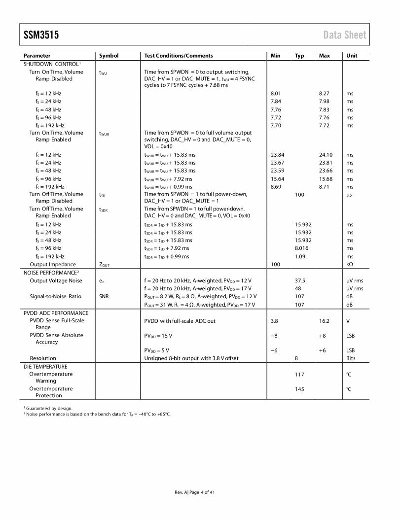
SSM3515 Data Sheet
Rev. A| Page 4 of 41
Parameter Symbol Test Conditions/Comments Min Typ Max Unit
SHUTDOWN CONTROL1 Turn On Time, Volume
Ramp Disabled tWU Time from SPWDN = 0 to output switching,
DAC_HV = 1 or DAC_MUTE = 1, tWU = 4 FSYNC cycles to 7 FSYNC cycles + 7.68 ms
fS = 12 kHz 8.01 8.27 ms fS = 24 kHz 7.84 7.98 ms
fS = 48 kHz 7.76 7.83 ms fS = 96 kHz 7.72 7.76 ms fS = 192 kHz 7.70 7.72 ms
Turn On Time, Volume Ramp Enabled
tWUR Time from SPWDN = 0 to full volume output switching, DAC_HV = 0 and DAC_MUTE = 0, VOL = 0x40
fS = 12 kHz tWUR = tWU + 15.83 ms 23.84 24.10 ms fS = 24 kHz tWUR = tWU + 15.83 ms 23.67 23.81 ms fS = 48 kHz tWUR = tWU + 15.83 ms 23.59 23.66 ms
fS = 96 kHz tWUR = tWU + 7.92 ms 15.64 15.68 ms fS = 192 kHz tWUR = tWU + 0.99 ms 8.69 8.71 ms
Turn Off Time, Volume Ramp Disabled
tSD Time from SPWDN = 1 to full power-down, DAC_HV = 1 or DAC_MUTE = 1
100 µs
Turn Off Time, Volume Ramp Enabled
tSDR Time from SPWDN = 1 to full power-down, DAC_HV = 0 and DAC_MUTE = 0, VOL = 0x40
fS = 12 kHz tSDR = tSD + 15.83 ms 15.932 ms fS = 24 kHz tSDR = tSD + 15.83 ms 15.932 ms fS = 48 kHz tSDR = tSD + 15.83 ms 15.932 ms fS = 96 kHz tSDR = tSD + 7.92 ms 8.016 ms
fS = 192 kHz tSDR = tSD + 0.99 ms 1.09 ms Output Impedance ZOUT 100 kΩ
NOISE PERFORMANCE2 Output Voltage Noise en f = 20 Hz to 20 kHz, A-weighted, PVDD = 12 V 37.5 µV rms f = 20 Hz to 20 kHz, A-weighted, PVDD = 17 V 48 µV rms Signal-to-Noise Ratio SNR POUT = 8.2 W, RL = 8 Ω, A-weighted, PVDD = 12 V 107 dB
POUT = 31 W, RL = 4 Ω, A-weighted, PVDD = 17 V 107 dB
PVDD ADC PERFORMANCE PVDD Sense Full-Scale
Range PVDD with full-scale ADC out 3.8 16.2 V
PVDD Sense Absolute Accuracy
PVDD = 15 V −8 +8 LSB
PVDD = 5 V −6 +6 LSB Resolution Unsigned 8-bit output with 3.8 V offset 8 Bits
DIE TEMPERATURE Overtemperature
Warning 117 °C
Overtemperature Protection
145 °C
1 Guaranteed by design. 2 Noise performance is based on the bench data for TA = −40°C to +85°C.
Data Sheet SSM3515
Rev. A| Page 5 of 41
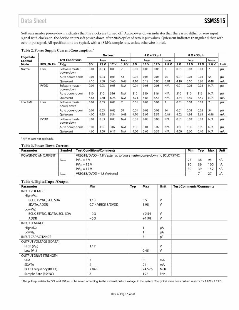
Software master power-down indicates that the clocks are turned off. Auto power-down indicates that there is no dither or zero input signal with clocks on; the device enters soft power-down after 2048 cycles of zero input values. Quiescent indicates triangular dither with zero input signal. All specifications are typical, with a 48 kHz sample rate, unless otherwise noted.
Table 2. Power Supply Current Consumption 1
Edge Rate Control Mode REG_EN Pin
Test Conditions
No Load 4 Ω + 15 µH 8 Ω + 33 µH
Unit IPVDD IREG18 IPVDD IREG18 IPVDD IREG18
PVDD 5 V 12 V 17 V 1.8 V 5 V 12 V 17 V 1.8 V 5 V 12 V 17 V 1.8 V
Normal Low Software master power-down
0.01 0.03 0.03 7 0.01 0.03 0.03 7 0.01 0.03 0.03 7 μA
Auto power-down 0.01 0.03 0.03 54 0.01 0.03 0.03 54 0.01 0.03 0.03 54 μA Quiescent 4.10 5.00 5.60 0.48 4.10 5.12 5.90 0.48 4.10 5.10 5.80 0.48 mA PVDD Software master
power-down 0.01 0.03 0.03 N/A 0.01 0.03 0.03 N/A 0.01 0.03 0.03 N/A μA
Auto power-down 310 310 316 N/A 310 310 316 N/A 310 310 316 N/A μA Quiescent 4.64 5.60 6.26 N/A 4.74 5.85 6.55 N/A 4.74 5.85 6.55 N/A mA Low EMI Low Software master
power-down 0.01 0.03 0.03 7 0.01 0.03 0.03 7 0.01 0.03 0.03 7 μA
Auto power-down 0.01 0.03 0.03 54 0.01 0.03 0.03 54 0.01 0.03 0.03 54 μA Quiescent 4.00 4.95 5.54 0.48 4.70 3.99 5.59 0.48 4.02 4.98 5.63 0.48 mA
PVDD Software master power-down
0.01 0.03 0.03 N/A 0.01 0.03 0.03 N/A 0.01 0.03 0.03 N/A μA
Auto power-down 310 310 316 N/A 310 310 316 N/A 310 310 316 N/A μA Quiescent 4.60 5.60 6.17 N/A 4.60 5.65 6.35 N/A 4.60 5.60 6.40 N/A mA 1 N/A means not applicable.
Table 3. Power-Down Current Parameter Symbol Test Conditions/Comments Min Typ Max Unit
POWER-DOWN CURRENT VREG18/DVDD = 1.8 V external, software master power-down, no BCLK/FSYNC IPVDD PVDD = 5 V 27 38 95 nA PVDD = 12 V 30 39 100 nA PVDD = 17 V 30 39 152 nA IDVDD VREG18/DVDD = 1.8 V external 7 27 μA
Table 4. Digital Input/Output Parameter Min Typ Max Unit Test Comments/Comments INPUT VOLTAGE1
High (VIH) BCLK, FSYNC, SCL, SDA 1.13 5.5 V SDATA, ADDR 0.7 × VREG18/DVDD 1.98 V
Low (VIL) BCLK, FSYNC, SDATA, SCL, SDA −0.3 +0.54 V ADDR −0.3 +1.98 V
INPUT LEAKAGE High (IIH) 1 µA Low (IIL) 1 µA
INPUT CAPACITANCE 5 pF OUTPUT VOLTAGE (SDATA)
High (VOH) 1.17 V Low (VOL) 0.45 V
OUTPUT DRIVE STRENGTH1 SDA 3 5 mA SDATA 2 24 mA BCLK Frequency (BCLK) 2.048 24.576 MHz Sample Rate (FSYNC) 8 192 kHz
1 The pull-up resistor for SCL and SDA must be scaled according to the external pull-up voltage in the system. The typical value for a pull-up resistor for 1.8 V is 2.2 kΩ.

SSM3515 Data Sheet
Rev. A| Page 6 of 41
DIGITAL TIMING CHARACTERISTICS All timing specifications are given for the default setting (I2S mode) of the serial input port.
Table 5. I2C Port Timing Limit
Parameter Min Max Unit Description
I2C PORT
fSCL 400 kHz SCL frequency tSCLH 0.6 µs SCL high tSCLL 1.3 µs SCL low tSCS 0.6 µs Setup time; relevant for repeated start condition
tSCH 0.6 µs Hold time; after this period, the first clock is generated tDS 100 ns Data setup time tSCR 300 ns SCL rise time tSCF 300 ns SCL fall time
tR 300 ns SDA rise time, not shown in Figure 2 tF 300 ns SDA fall time, not shown in Figure 2 tBFT 0.6 µs Bus-free time (time between stop and start) tHOLD 140 ns SCL falling to SDA rising
0 ns SCL falling to SDA falling
Table 6. Digital Input Timing Limit
Parameter TMIN TMAX Unit Description
SERIAL PORT tBIL 15 ns BCLK low pulse width tBIH 15 ns BCLK high pulse width tSIS 6 ns SDATA setup, time to BCLK rising
tSIH 6 ns SDATA hold, time from BCLK rising tLIS 10 ns FSYNC setup time to BCLK rising tLIH 5 ns FSYNC hold time to BCLK rising tBP 40 ns Minimum BCLK period
Digital Timing Diagrams tSCH
tSCS
tBFTtSCF
tDS
tSCLL
tHOLD
tSCR
tSCLH
tSCH
STOPCONDITION
STARTCONDITION
SDA
SCL
1332
7-00
5
Figure 2. I2C Port Timing

Data Sheet SSM3515
Rev. A| Page 7 of 41
tSIS
tSIH
tSIS
tSIH
tLIH
tBPtBIH
BCLK
FSYNC
SDATALEFT-JUSTIFIED
MODE
SDATAI2C-JUSTIFIED
MODE
SDATARIGHT-JUSTIFIED
MODE
tBIL
tLIS
tSIS
tSIH
tSIS
tSIH
MSB
MSB
MSB LSB
MSB – 1
1332
7-00
2
Figure 3. Serial Input Port Timing
PVDD
PVDD/2
tWU
I2C POWER-UP COMMAND
OUTPUT
0V13
327-
161
Figure 4. Turn On Hard Volume
tSD
I2C POWER-DOWN COMMAND
OUTPUT
PVDD
0V
1332
7-16
2
Figure 5. Turn Off Hard Volume

SSM3515 Data Sheet
Rev. A| Page 8 of 41
ABSOLUTE MAXIMUM RATINGS Absolute maximum ratings apply at TA = 25°C, unless otherwise noted.
Table 7. Parameter Rating
PVDD Supply Voltage −0.3 V to +18 V
VREG18/DVDD Supply Voltage −0.3 V to +1.98 V VREG50/AVDD Supply Voltage −0.3 V to +5.5 V PGND and AGND Differential ±0.3 V ADDR, SDATA Input Voltage −0.3 V to +1.98 V SCL, SDA, BCLK, FSYNC Input Voltage −0.3 V to +5.5 V
REG_EN Input Voltage −0.3 V to +18 V Storage Temperature Range −65°C to +150°C Operating Temperature Range −40°C to +85°C Junction Temperature Range −65°C to +165°C Lead Temperature Range
(Soldering, 60 sec) 300°C
Stresses at or above those listed under Absolute Maximum Ratings may cause permanent damage to the product. This is a stress rating only; functional operation of the product at these or any other conditions above those indicated in the operational section of this specification is not implied. Operation beyond the maximum operating conditions for extended periods may affect product reliability.
THERMAL RESISTANCE θJA (junction to air) is specified for worst case conditions, that is, a device soldered in a circuit board for surface-mount packages. θJA and θJB are determined according to JESD51-9 on a 4-layer printed circuit board (PCB) with natural convection cooling.
Table 8. Thermal Resistance Package Type θJA Unit
20-Ball, 1.8 mm × 2.2 mm WLCSP 55.5 °C/W
ESD CAUTION

Data Sheet SSM3515
Rev. A| Page 9 of 41
PIN CONFIGURATION AND FUNCTION DESCRIPTIONS 1 2 3 4
A
B
C
D
VREG50/AVDD
AGND PGND BST–
SDA ADDR OUT– OUT–
SCL REG_EN PVDD PVDD
VREG18/DVDD
FSYNC OUT+ OUT+
SDATA BCLK PGND BST+E
1332
7-00
6
Figure 6. Pin Configuration (Top Side View)
Table 9. Pin Function Descriptions Pin No. Mnemonic Type1 Description A1 VREG50/AVDD AOUT 5 V Regulator Output. A2 AGND PWR Analog Ground. It is recommended to connect the AGND pin to a single ground plane on the board. A3 PGND PWR Power Stage Ground. The PGND pin is shorted internally. It is recommended to connect PGND to a
single ground plane on the board. A4 BST− AIN Bootstrap Capacitor for OUT−. B1 SDA DIO I2C Serial Data. B2 ADDR DIN I2C Address Selection. B3 OUT− AOUT Power Stage Inverting Output. B4 OUT− AOUT Power Stage Inverting Output. C1 SCL DIN I2C Clock. C2 REG_EN AIN Regulator Enable Tie to PVDD to Enable Regulators. C3 PVDD PWR Power Stage Supply. C4 PVDD PWR Power Stage Supply. D1 VREG18/DVDD PWR 1.8 V Regulator Output/DVDD Input. D2 FSYNC DIN TDM Frame Sync Input. D3 OUT+ AOUT Power Stage Noninverting Output. D4 OUT+ AOUT Power Stage Noninverting Output. E1 SDATA DIO Serial Data Input to DAC. E2 BCLK DIN TDM Bit Clock Input. E3 PGND PWR Power Stage Ground. The PGND pin is shorted internally. It is recommended to connect PGND to a
single ground plane on the board. E4 BST+ AIN Bootstrap Capacitor for OUT+.
1 AOUT is analog output; PWR is power supply or ground pin; AIN is analog input; DIO is digital input/output; DIN is digital input.
SSM3515 Data Sheet
Rev. A| Page 10 of 41
TYPICAL PERFORMANCE CHARACTERISTICS
–180
20
–170–160–150–140–130–120–110–100
–90–80–70–60–50–40–30–20–10
010
20 100 1k 10k
FREQUENCY (Hz)
AM
PL
ITU
DE
(d
BV
)
1332
7-10
1
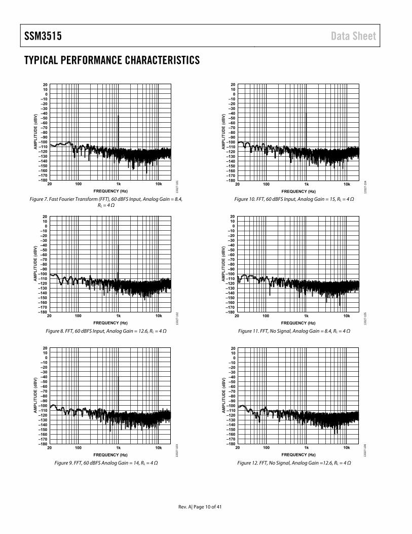
Figure 7. Fast Fourier Transform (FFT), 60 dBFS Input, Analog Gain = 8.4, RL = 4 Ω
–180
20
–170–160–150–140–130–120–110–100–90–80–70–60–50–40–30–20–10
010
20 100 1k 10k
FREQUENCY (Hz)
AM
PL
ITU
DE
(d
BV
)
1332
7-10
2
Figure 8. FFT, 60 dBFS Input, Analog Gain = 12.6, RL = 4 Ω
–180
20
–170–160–150–140–130–120–110–100–90–80–70–60–50–40–30–20–10
010
20 100 1k 10k
FREQUENCY (Hz)
AM
PL
ITU
DE
(d
BV
)
1332
7-10
3
Figure 9. FFT, 60 dBFS Analog Gain = 14, RL = 4 Ω
–180
20
–170–160–150–140–130–120–110–100
–90–80–70–60–50–40–30–20–10
010
20 100 1k 10k
FREQUENCY (Hz)
AM
PL
ITU
DE
(d
BV
)
1332
7-10
4
Figure 10. FFT, 60 dBFS Input, Analog Gain = 15, RL = 4 Ω
–180
20
–170–160–150–140–130–120–110–100
–90–80–70–60–50–40–30–20–10
010
20 100 1k 10k
FREQUENCY (Hz)
AM
PL
ITU
DE
(d
BV
)
1332
7-10
5
Figure 11. FFT, No Signal, Analog Gain = 8.4, RL = 4 Ω
–180
20
–170–160–150–140–130–120–110–100–90–80–70–60–50–40–30–20–10
010
20 100 1k 10k
FREQUENCY (Hz)
AM
PL
ITU
DE
(d
BV
)
1332
7-10
6
Figure 12. FFT, No Signal, Analog Gain =12.6, RL = 4 Ω

Data Sheet SSM3515
Rev. A| Page 11 of 41
20 100 1k 10k
FREQUENCY (Hz)
–180
20
–170–160–150–140–130–120–110–100
–90–80–70–60–50–40–30–20–10
010
AM
PLIT
UD
E (d
BV)
1332
7-10
7
Figure 13. FFT, No Signal, Analog Gain = 14, RL = 4 Ω
20 100 1k 10k
FREQUENCY (Hz)
–180
20
–170–160–150–140–130–120–110–100–90–80–70–60–50–40–30–20–10
010
AM
PLIT
UD
E (d
BV)
1332
7-10
8
Figure 14. FFT, No Signal, Analog Gain = 15, RL = 4 Ω
0.001
1
0.01
0.1
20 100 1k 10k
FREQUENCY (Hz)
THD
+ N
(%)
100mW1W
1332
7-00
7
Figure 15. THD + N vs. Frequency into RL = 4 Ω, PVDD = 4.5 V
FREQUENCY (Hz)
0.001
1
0.01
0.1
20 100 1k 10k
THD
+ N
(%)
100mW1W5W
1332
7-00
8
Figure 16. THD + N vs. Frequency, RL = 4 Ω, PVDD = 12 V
FREQUENCY (Hz)
20 100 1k 10k0.001
1
0.01
0.1
THD
+ N
(%)
100mW1W10W
1332
7-00
9
Figure 17. THD + N vs. Frequency, RL = 4 Ω, PVDD = 17 V
FREQUENCY (Hz)
20 100 1k 10k0.001
1
0.01
0.1
THD
+ N
(%)
100mW1W
1332
7-01
0
Figure 18. THD + N vs. Frequency, RL = 8 Ω, PVDD = 4.5 V
SSM3515 Data Sheet
Rev. A| Page 12 of 41
FREQUENCY (Hz)
20 100 1k 10k0.001
1
0.01
0.1
THD
+ N
(%)
100mW1W5W
1332
7-01
1
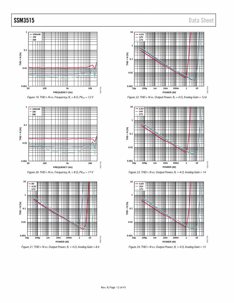
Figure 19. THD + N vs. Frequency, RL = 8 Ω, PVDD = 12 V
FREQUENCY (Hz)
20 100 1k 10k0.001
1
0.01
0.1
THD
+ N
(%)
100mW1W5W
1332
7-01
2
Figure 20. THD + N vs. Frequency, RL = 8 Ω, PVDD = 17 V
THD
+ N
(%)
0.001
10
0.01
0.1
1
10µ 100µ 1m 10m 100m 1 10
POWER (W)
8V4.5V17V
1332
7-01
3
Figure 21. THD + N vs. Output Power, RL = 4 Ω, Analog Gain = 8.4
THD
+ N
(%)
0.001
10
0.01
0.1
1
10µ 100µ 1m 10m 100m 1 10
POWER (W)
4.5V12V17V
1332
7-01
4
Figure 22. THD + N vs. Output Power, RL = 4 Ω, Analog Gain = 12.6
THD
+ N
(%)
0.001
10
0.01
0.1
1
10µ 100µ 1m 10m 100m 1 10
POWER (W)
4.5V14V17V
1332
7-01
5
Figure 23. THD + N vs. Output Power, RL = 4 Ω, Analog Gain = 14
THD
+ N
(%)
0.001
10
0.01
0.1
1
10µ 100µ 1m 10m 100m 1 10
POWER (W)
4.5V15V17V
1332
7-01
6
Figure 24. THD + N vs. Output Power, RL = 4 Ω, Analog Gain = 15

Data Sheet SSM3515
Rev. A| Page 13 of 41
TH
D +
N (
%)
0.001
10
0.01
0.1
1
10µ 100µ 1m 10m 100m 1 10
POWER (W)
4.5V14V17V
1332
7-01
7
Figure 25. THD + N vs. Output Power, RL = 8 Ω, Analog Gain = 8.4
TH
D +
N (
%)
0.001
10
0.01
0.1
1
10µ 100µ 1m 10m 100m 1 10
POWER (W)
4.5V12V14V
1332
7-01
8
Figure 26. THD + N vs. Output Power, RL = 8 Ω, Analog Gain = 12.6
TH
D +
N (
%)
0.001
10
0.01
0.1
1
10µ 100µ 1m 10m 100m 1 10
POWER (W)
4.5V14V16V
1332
7-01
9
Figure 27. THD + N vs. Output Power, RL = 8 Ω, Analog Gain = 14
TH
D +
N (
%)
10µ 100µ 1m 10m 100m 1 10
POWER (W)
0.001
10
0.01
0.1
1
4.5V15V17V
1332
7-02
0
Figure 28. THD + N vs. Output Power, RL = 8 Ω, Analog Gain = 15
PO
WE
R (
W)
14
5 6 7 8 9 10
PVDD (V)
11 12 13 14
10
12
8
6
4
2
0
POUT 10%, 8V GAINPOUT 1%, 8V GAIN
1332
7-02
1
Figure 29. Output Power vs. PVDD Supply Voltage (PVDD), RL = 4 Ω, Analog Gain = 8.4
PO
WE
R (
W)
30
5 6 7 8 9 10
PVDD (V)
11 12 13 14 15 16 17
20
25
15
10
5
0
POUT 10%POUT 1%
1332
7-02
2
Figure 30. Output Power vs. PVDD, RL = 4 Ω, Analog Gain = 12.6

SSM3515 Data Sheet
Rev. A| Page 14 of 41
PO
WE
R (
W)
35
30
5 6 7 8 9 10
PVDD (V)
11 12 13 14 15 16 17
20
25
15
10
5
0
POUT 10%POUT 1%
1332
7-02
3Figure 31. Output Power vs. PVDD, RL = 4 Ω, Analog Gain = 14
PO
WE
R (
W)
40
5 6 7 8 9 10
PVDD (V)
11 12 13 14 15 16 17
20
25
30
35
15
10
5
0
POUT 10%POUT 1%
1332
7-02
4
Figure 32. Output Power vs. PVDD, RL = 4 Ω, Analog Gain = 15
0
10
20
30
40
50
60
70
80
90
100
0 0.5 1.0 1.5 2.0 2.5 3.0 3.5 4.0 4.5 5.0
EF
FIC
IEN
CY
(%
)
POUT (W)
5V NO FB NORMAL5V NO FB LOW
1332
7-02
5
Figure 33. Efficiency vs. Output Power (POUT), RL = 4 Ω, No Ferrite Bead (FB) and 220 pF Capacitor, PVDD = 5 V, Analog Gain = 8.4
0
10
20
30
40
50
60
70
80
90
100
0 0.5 1.0 1.5 2.0 2.5 3.0 3.5 4.0 4.5 5.0
EF
FIC
IEN
CY
(%
)
POUT (W)
5V FB NORMAL5V FB LOW
1332
7-02
6
Figure 34. Efficiency vs. POUT, RL = 4 Ω, FB and 220 pF Capacitor, PVDD = 5 V, Analog Gain = 8.4
0 5 10 15 20 250
10
20
30
40
50
60
70
80
90
100
0
EF
FIC
IEN
CY
(%
)
POUT (W)
12V NO FB NORMAL12V NO FB LOW
1332
7-02
7
Figure 35. Efficiency vs. POUT, RL = 4 Ω, No FB and 220 pF, PVDD = 12 V, Analog Gain = 12.6
0 5 10 15 20 250
10
20
30
40
50
60
70
80
90
100
0
EF
FIC
IEN
CY
(%
)
POUT (W)
12V FB NORMAL12V FB LOW
1332
7-02
8
Figure 36. Efficiency vs. POUT, RL = 4 Ω, FB and 220 pF Capacitor, PVDD = 12 V, Analog Gain = 12.6

Data Sheet SSM3515
Rev. A| Page 15 of 41
0 5 10 15 20 25 30 35 400
10
20
30
40
50
60
70
80
90
100
EFFI
CIE
NC
Y (%
)
POUT (W)
17V FB NORMAL17V FB LOW
1332
7-02
9
Figure 37. Efficiency vs. POUT, RL = 4 Ω, FB and 220 pF Capacitor, PVDD = 17 V,
Analog Gain = 14
0 5 10 15 20 25 30 35 45400
10
20
30
40
50
60
70
80
90
100
EFFI
CIE
NC
Y (%
)
POUT (W)
17V NO FB NORMAL17V NO FB LOW
1332
7-03
0
Figure 38. Efficiency vs. POUT, RL = 4 Ω, No FB and 220 pF Capacitor, PVDD = 17 V,
Analog Gain = 14
0
0.001
0.002
0.003
0.004
0.005
0.006
0.007
5 7 9 11 13 15 17
I PVD
D (A
MP)
PVDD (V)
NO LOAD NO FB NORMAL MODENO LOAD NO FB LOW MODE
1332
7-03
1
Figure 39. Quiescent Current, RL = 4 Ω, No FB and 220 pF Capacitor,
Analog Gain = 12
0
0.001
0.002
0.003
0.004
0.005
0.006
0.007
0.008
0.009
0.010
5 7 9 11 13 15 17 19
I PVD
D (A
)
PVDD (V)
4Ω + 15µH FB 220pF LOW MODE4Ω + 15µH FB 220pF NORMAL MODE
1332
7-03
2
Figure 40. Quiescent Current, RL = 4 Ω, FB and 220 pF Capacitor,
Analog Gain = 12
0
1
2
3
4
5
6
7
5 6 7 8 9 10 11 12 13 14
POW
ER (W
)
PVDD (V)
POUT 10%POUT 1%
1332
7-03
3
Figure 41. Output Power vs. PVDD, RL = 8 Ω, Analog Gain = 8
0
2
4
6
8
10
12
14
5.0 107.5 12.5
POW
ER (W
)
PVDD (V)
POUT 10%POUT 1%
1332
7-03
4
Figure 42. Output Power vs. PVDD, RL = 8 Ω, Analog Gain = 12

SSM3515 Data Sheet
Rev. A| Page 16 of 41
0
2
4
6
8
10
12
14
16
18
5 10 15
POW
ER (W
)
PVDD (V)
POUT 10%POUT 1%
1332
7-03
5
Figure 43. Output Power vs. PVDD, RL = 8 Ω, Analog Gain = 14
0
5
10
15
20
5 10 15
POW
ER (W
)
PVDD (V)
POUT 10%POUT 1%
1332
7-03
6
Figure 44. Output Power vs. PVDD, RL = 8 Ω, Analog Gain = 15
100
0
20
40
60
80
0 1 2 3
EFFI
CIE
NC
Y (%
)
POUT (W)
1332
7-03
7
5V NO FB NORMAL5V NO FB LOW
Figure 45. Efficiency vs. POUT, RL = 8 Ω, No FB and 220 pF Capacitor,
PVDD = 5 V, Analog Gain = 8.4
0
20
40
60
80
100
10
30
50
70
90
EFFI
CIE
NC
Y (%
)
POUT (W)
0 2 4 6 8 10 12
NORMAL NO FB/220pFLOW NO FB/220pF
1332
7-03
8
Figure 46. Efficiency vs. POUT, RL = 8 Ω, No FB and 220 pF Capacitor,
PVDD = 12 V, Analog Gain = 12.6
EFFI
CIE
NC
Y (%
)
POUT (W)
0
20
40
60
80
100
0 5 10 15 20
17V NO FB NORMAL17V NO FB LOW
1332
7-04
1
Figure 47. Efficiency vs. POUT, RL = 8 Ω, No FB and 220 pF Capacitor,
PVDD = 17 V, Analog Gain = 14
0
10
20
30
40
50
60
70
80
90
100
0 1 2 3
EFFI
CIE
NC
Y (%
)
POUT (W)
5V NO FB NORMAL5V NO FB LOW
1332
7-04
0
Figure 48. Efficiency vs. POUT, RL = 8 Ω, FB and 220 pF Capacitor,
PVDD = 5 V, Analog Gain = 8.4

Data Sheet SSM3515
Rev. A| Page 17 of 41
0
10
20
30
40
50
60
70
80
90
100
0 2 4 6 8 10 12 14
EFFI
CIE
NC
Y (%
)
POUT (W)
NORMAL FB/220pFLOW FB/220pF
1332
7-03
9
Figure 49. Efficiency vs. POUT, RL = 8 Ω, FB and 220 pF Capacitor,
PVDD = 12 V, Analog Gain = 12.6
0
20
40
60
80
100
0 5 10 15 20
EFFI
CIE
NC
Y (%
)
POUT (W)
17V FB LOW17V FB NORMAL
1332
7-04
2
Figure 50. Efficiency vs. POUT, RL = 8 Ω, FB and 220 pF Capacitor, PVDD = 17 V,
Analog Gain = 14
0
20
40
60
80
100
0 2 4 6
EFFI
CIE
NC
Y (%
)
POUT (W)
5V NO FB NORMAL5V NO FB LOW
1332
7-04
5
Figure 51. Efficiency vs. POUT, RL = 3 Ω, No FB and 220 pF Capacitor,
PVDD = 5 V, Analog Gain = 8.4
0
20
40
60
80
100
0 10 20 30
EFFI
CIE
NC
Y (%
)
POUT (W)
12V NO FB NORMAL12V NO FB LOW
1332
7-04
6
Figure 52. Efficiency vs. POUT, RL = 3 Ω, No FB and 220 pF Capacitor,
PVDD = 12 V, Analog Gain = 12.6
0
20
40
60
80
100
0 5 10 15 20 25 30 35 40 45 50
EFFI
CIE
NC
Y (%
)
POUT (W)
17V NO FB NORMAL17V NO FB LOW
1332
7-04
7
Figure 53. Efficiency vs. POUT, RL = 3 Ω, No FB and 220 pF Capacitor,
PVDD = 17 V, Analog Gain = 14
0
20
40
60
80
100
0 2 4 6
EFFI
CIE
NC
Y (%
)
POUT (W)
5V FB NORMAL5V FB LOW
1332
7-04
8
Figure 54. Efficiency vs. POUT, RL = 3 Ω, FB and 220 pF Capacitor, PVDD = 5 V,
Analog Gain = 8.4
SSM3515 Data Sheet
Rev. A| Page 18 of 41
0
20
40
60
80
100
0 10 20 30
EFFI
CIE
NC
Y (%
)
POUT (W)
12V FB NORMAL12V FB LOW
1332
7-04
9
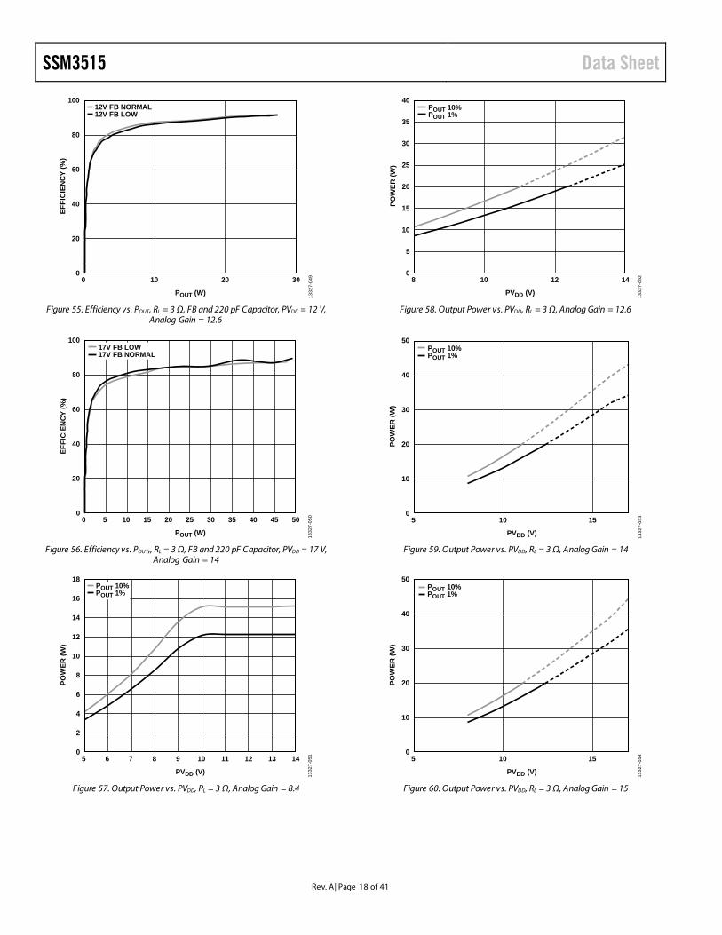
Figure 55. Efficiency vs. POUT, RL = 3 Ω, FB and 220 pF Capacitor, PVDD = 12 V,
Analog Gain = 12.6
0
20
40
60
80
100
0 5 10 15 20 25 30 35 40 45 50
EFFI
CIE
NC
Y (%
)
POUT (W)
17V FB LOW17V FB NORMAL
1332
7-05
0
Figure 56. Efficiency vs. POUT,, RL = 3 Ω, FB and 220 pF Capacitor, PVDD = 17 V,
Analog Gain = 14
0
2
4
6
8
10
12
14
16
18
5 6 7 8 9 10 11 12 13 14
POW
ER (W
)
PVDD (V)
POUT 10%POUT 1%
1332
7-05
1
Figure 57. Output Power vs. PVDD, RL = 3 Ω, Analog Gain = 8.4
POW
ER (W
)
0
5
10
15
20
25
30
35
40
8 10 12 14
PVDD (V)
POUT 10%POUT 1%
1332
7-05
2
Figure 58. Output Power vs. PVDD, RL = 3 Ω, Analog Gain = 12.6
POW
ER (W
)
0
10
20
30
40
50
5 10 15
PVDD (V)
POUT 10%POUT 1%
1332
7-05
3
Figure 59. Output Power vs. PVDD, RL = 3 Ω, Analog Gain = 14
POW
ER (W
)
0
10
20
30
40
50
5 10 15
PVDD (V)
POUT 10%POUT 1%
1332
7-05
4
Figure 60. Output Power vs. PVDD, RL = 3 Ω, Analog Gain = 15

Data Sheet SSM3515
Rev. A| Page 19 of 41
THEORY OF OPERATION OVERVIEW The SSM3515 Class-D audio amplifier features a filterless modulation scheme that greatly reduces the external component count, conserving board space and reducing system cost. The SSM3515 does not require an output filter; it relies on the inherent inductance of the speaker coil and the natural filtering of the speaker and human ear to recover the audio component of the square wave output.
Most Class-D amplifiers use some variation of pulse-width modulation (PWM), but the SSM3515 uses Σ-Δ modulation to determine the switching pattern of the output devices, resulting in a number of important benefits. Σ-Δ modulators do not produce a sharp peak with many harmonics in the AM broadcast band, as pulse-width modulators often do. Σ-Δ modulation reduces the amplitude of spectral components at high frequencies, reducing EMI emission that may otherwise be radiated by speakers and long cable traces. Due to the inherent spread spectrum nature of Σ-Δ modulation, the need for oscillator synchronization is elimi-nated for designs incorporating multiple SSM3515 amplifiers.
The SSM3515 also integrates overcurrent and temperature protection and a thermal warning with optional programmable gain reduction.
POWER SUPPLIES The power supply pins on the SSM3515 are PVDD, VREG50/ AVDD, and VREG18/DVDD.
PVDD, the battery supply, is used for the output stage and also supplies power to the 5 V regulator. In addition, it can be used to supply power to the 1.8 V regulator. This pin must be decoupled to ground using a 100 nF capacitor in parallel with a 1 µF MLCC capacitor to ground as close as possible to the respective pins. In addition, a bulk electrolytic capacitor may be required depending on the output power to supply the current at low frequency output. Typically, 220 µF and 25 V is recommended. This must be sized according to the power supply regulation in the system.
VREG50/AVDD (5 V) is the analog supply used for the input stage, modulator, power stage driver, and other blocks. It uses the VREG50/AVDD pin. It is generated internally by the integrated 5 V linear regulator. This pin must be decoupled to ground using the 100 nF and 10 µF capacitor.
VREG18/DVDD (1.8 V) is the supply for the digital circuitry. It uses the VREG18/DVDD pin. It can be generated internally using an integrated 1.8 V linear regulator. Alternatively, an external 1.8 V supply can be used to save the power dissipation. The VREG18/DVDD pin must be decoupled to ground using 100 nF and 10 µF MLCC capacitors close to the pin.
POWER-UP SEQUENCE If the REG_EN pin is tied to PVDD, the power-up sequence is performed internally. As the PVDD voltage ramps up, the VREG18/DVDD voltage (generated internally) also ramps up. The typical wait time before the I2C commands can be sent to the device depends on the PVDD supply ramp-up time.
If the REG_EN pin is tied low, ensure that 1.8 V is supplied externally and that PVDD is greater than 4.5 V before sending I2C commands to enable the device.
POWER-DOWN OPERATION The SSM3515 offers several power down options via I2C. Register 0x00 provides multiple options for setting the various power-down modes.
Set the SPWDN bit to 1 to fully power down the device. Only the I2C, 1.8 V regulator is kept alive.
The SSM3515 monitors both the BCLK and FSYNC pins for clock presence when in 2-wire mode. When no BCLK or FSYNC signals are present, the device automatically powers down all internal circuitry to its lowest power state. When a BCLK or FSYNC signal returns, the device automatically powers up following its usual power up sequence.
When enabled, the APWDN_EN bit (auto power down), activates a low power state as soon as 2048 consecutive zero input samples are received. Only the I2C and digital audio input blocks are kept active.
REG_EN PIN SETUP AND CONTROL The REG_EN (regulator enable) pin enables or disables the internal 1.8 V regulator.
Table 10. Regulator Enable Pin Function REG_EN 1.8 V Regulator Comment
Ground Disabled External 1.8 V
PVDD Enabled Internal 1.8 V
The status of the REG_EN pin determines if the 1.8 V supply is generated internally or if it must be provided externally. If the REG_EN pin is tied to PVDD, the internal 1.8 V regulator is enabled. If the REG_EN pin is tied to ground, a 1.8 V supply must be supplied externally to the VREG18/DVDD pin for the device to operate. For the device to respond to I2C commands, the 1.8 V supply must be stable.

SSM3515 Data Sheet
Rev. A| Page 20 of 41
ADDR PIN SETUP AND CONTROL The ADDR pin sets the device I2C address. See Table 11 for details.
CLOCKING In 3-wire mode (BCLK, FSYNC, SDATA), a BCLK signal must be provided to the SSM3515 for correct operation. The BCLK
signal must have a minimum frequency of 2.048 MHz. The BCLK signal is used for internal clocking of the device. The BCLK rate is detected automatically, but the sampling frequency must be known to the device. The supported BCLK rates at 32 kHz to 48 kHz are 50, 64, 100, 128, 192, 200, 256, 384, 400, and 512 times the sample rate.
Table 11. Pin Setup List ADDR Pin SCL Pin SDA Pin Control Mode 7-Bit I2C Address TDM Slot
Connected to Ground Using a 47 kΩ Resistor SCL SDA I2C 0x14 1 Open (No Connection) SCL SDA I2C 0x15 2 Connected to 1.8 V Using a 47 kΩ Resistor SCL SDA I2C 0x16 3 Connected to 1.8 V SCL SDA I2C 0x17 4

Data Sheet SSM3515
Rev. A| Page 21 of 41
DIGITAL AUDIO SERIAL INTERFACE The SSM3515 includes a standard serial audio interface that is slave only. The interface is capable of receiving I2S, left justified, PCM, or TDM formatted data.
The serial interface has three main operating modes, listed in Table 12.
Table 12. Operating Modes Mode Format Comments
2-Channel (Stereo) I2S/left justified Register control using I2C port
Multichannel TDM I2S/left justified Register control using I2C port
Stereo modes, typically I2S or left justified, are used when there is one or two devices on the interface bus. Standard multi-channel TDM modes are more flexible and offer the ability to have multiple devices on the bus. In both of these cases, the register control uses an I2C port.
STEREO (I2S/LEFT JUSTIFIED) OPERATING MODE Stereo modes use both edges of FSYNC to determine placement of data. Stereo mode is enabled when SAI_MODE = 0 and the data format is determined by the SDATA_FMT register setting.
The I2S or left justified interface formats accept any number of BCLK cycles per FSYNC cycle. Sample rates from 8 kHz to 192 kHz are accepted. The maximum BCLK rate is 24.576 MHz.
TDM OPERATING MODE The TDM operating mode allows multiple chips to use a single serial interface bus for audio data.
The FSYNC signal operates at the desired sample rate. A rising edge of the FSYNC signal indicates the start of a new frame. For proper operation, this signal must be one BCLK cycle wide, transitioning on a falling BCLK edge. The MSB of data must be present on the SDATA one BCLK cycle later. The SDATA signal latches on the rising edge of BCLK.
Each chip on the TDM bus can occupy 16, 24, 32, 48, or 64 BCLK cycles. This is set with the TDM_BCLKS bits and all devices on the bus must have the same setting. Up to 16 SSM3515 devices can be used on a single TDM bus, but only 4 unique I2C device addresses are available. The SSM3515 automatically determines how many possible devices can be placed on the bus from the BCLK rate. There is no limit to the total number of BCLK cycles per FSYNC pulse.
Which chip slot each SSM3515 uses is determined by the ADDR pin settings (see Table 11 for details), or by the TDM_SLOT bits in Register 0x05.
The input data width to the DAC can be either 16-bit or 24-bit.
I2C CONTROL The SSM3515 supports a 2-wire serial (I2C-compatible) microprocessor bus driving multiple peripherals. Two pins, serial data (SDA) and serial clock (SCL), carry information between the SSM3515 and the system I2C master controller. The SSM3515 is always a slave on the bus, meaning it cannot initiate a data transfer. Each slave device is recognized by a unique address. Using the ADDR pin provides the four device addresses, which are listed in Table 11. The address byte format is shown in Table 13. The address resides in the first seven bits of the I2C write. The LSB of this byte sets either a read or write operation. Logic Level 1 corresponds to a read operation, and Logic Level 0 corresponds to a write operation.
Connect 2.2 kΩ pull-up resistors on the lines connected to the SDA and SCL pins. The voltage on these signal lines must not be more than 5 V.
Addressing
Initially, each device on the I2C bus is in an idle state, monitoring the SDA and SCL lines for a start condition and the proper address. The I2C master initiates a data transfer by establishing a start condition, defined by a high to low transition on SDA while SCL remains high. This indicates that an address or data stream follows. All devices on the bus respond to the start condition and shift the next eight bits (the 7-bit address plus the R/W bit) MSB first. The device that recognizes the transmitted address responds by pulling the data line low during the ninth clock pulse. This ninth bit is an acknowledge bit. All other devices withdraw from the bus at this point and return to the idle con-dition. The device address for the SSM3515 is determined by the state of the ADDR pin. See Table 11 for four available addresses.
The R/W bit determines the direction of the data. A Logic 0 on the LSB of the first byte means the master writes information to the peripheral, whereas a Logic 1 means the master reads information from the peripheral after writing the subaddress and repeating the start address. A data transfer occurs until a stop condition is encountered. A stop condition occurs when SDA transitions from low to high while SCL is held high. The timing for the I2C port is shown in Figure 61.
Stop and start conditions can be detected at any stage during the data transfer. If these conditions are asserted out of sequence with normal read and write operations, the SSM3515 immediately jumps to the idle condition. During a given SCL high period, the user must issue only one start condition, one stop condition, or a single stop condition followed by a single start condition. If the user issues an invalid subaddress, the SSM3515 does not issue an acknowledge and returns to the idle condition. If the user exceeds the highest subaddress while in auto-increment mode, one of two actions is taken.
SSM3515 Data Sheet
Rev. A| Page 22 of 41
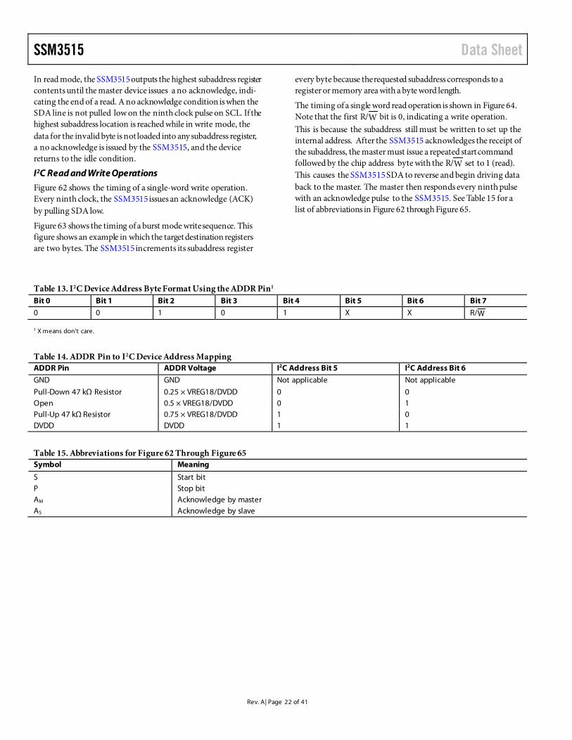
In read mode, the SSM3515 outputs the highest subaddress register contents until the master device issues a no acknowledge, indi-cating the end of a read. A no acknowledge condition is when the SDA line is not pulled low on the ninth clock pulse on SCL. If the highest subaddress location is reached while in write mode, the data for the invalid byte is not loaded into any subaddress register, a no acknowledge is issued by the SSM3515, and the device returns to the idle condition.
I2C Read and Write Operations
Figure 62 shows the timing of a single-word write operation. Every ninth clock, the SSM3515 issues an acknowledge (ACK) by pulling SDA low.
Figure 63 shows the timing of a burst mode write sequence. This figure shows an example in which the target destination registers are two bytes. The SSM3515 increments its subaddress register
every byte because the requested subaddress corresponds to a register or memory area with a byte word length.
The timing of a single word read operation is shown in Figure 64. Note that the first R/W bit is 0, indicating a write operation. This is because the subaddress still must be written to set up the internal address. After the SSM3515 acknowledges the receipt of the subaddress, the master must issue a repeated start command followed by the chip address byte with the R/W set to 1 (read). This causes the SSM3515 SDA to reverse and begin driving data back to the master. The master then responds every ninth pulse with an acknowledge pulse to the SSM3515. See Table 15 for a list of abbreviations in Figure 62 through Figure 65.
Table 13. I2C Device Address Byte Format Using the ADDR Pin1 Bit 0 Bit 1 Bit 2 Bit 3 Bit 4 Bit 5 Bit 6 Bit 7
0 0 1 0 1 X X R/W 1 X means don’t care.
Table 14. ADDR Pin to I2C Device Address Mapping ADDR Pin ADDR Voltage I2C Address Bit 5 I2C Address Bit 6
GND GND Not applicable Not applicable
Pull-Down 47 kΩ Resistor 0.25 × VREG18/DVDD 0 0 Open 0.5 × VREG18/DVDD 0 1 Pull-Up 47 kΩ Resistor 0.75 × VREG18/DVDD 1 0 DVDD DVDD 1 1
Table 15. Abbreviations for Figure 62 Through Figure 65 Symbol Meaning
S Start bit P Stop bit AM Acknowledge by master AS Acknowledge by slave

Data Sheet SSM3515
Rev. A| Page 23 of 41
R/W
SCK
SDA
SDA(CONTINUED)
SCK(CONTINUED)
START BYMASTER
FRAME 1CHIP ADDRESS BYTE
FRAME 2SUBADDRESS BYTE
FRAME 3DATA BYTE 1
FRAME 4DATA BYTE 2
STOP BYMASTER
ACK ACK
ACK ACK
1332
7-06
6
Figure 61. I2C Read/Write Timing
STARTBIT
STOPBIT
R/W = 0 ACK BYSLAVE
ACK BYSLAVE
I2C ADDRESS(7 BITS)
SUBADDRESS(8 BITS)
DATA BYTE 1(8 BITS)
1332
7-06
7
Figure 62. Single Word I2C Write Format
S CHIP ADDRESS,R/W = 0
SUBADDRESS DATAWORD 2
DATAWORD 1 ASASASAS … P
1332
7-06
8
Figure 63. Burst Mode I2C Write Format
S SCHIP ADDRESS,R/W = 0
CHIP ADDRESS,R/W = 1
SUBADDRESS AS AS AMAS PDATA
BYTE 1DATA
BYTE N
1332
7-06
9
Figure 64. Single Word I2C Read Format
…S SCHIP ADDRESS,R/W = 0
CHIP ADDRESS,R/W = 1
SUBADDRESS AS AS AMAS PDATA
WORD 1
1332
7-07
0
Figure 65. Burst Mode I2C Read Format

SSM3515 Data Sheet
Rev. A| Page 24 of 41
ANALOG AND DIGITAL GAIN Several selectable settings are available for the analog gain of the system. These provide optimal gain settings at various PVDD supply voltages. The ANA_GAIN bits are available in Register 0x01, Bits[1:0].
The available options are as shown in Table 16.
Table 16. Analog Gain Options
PVDD ANA_GAIN Amplifier Analog Gain Selection
5 V to 9 V 00 8.4 V full-scale gain mapping 9 V to 13 V 01 12.6 V full-scale gain mapping 13 V to 14 V 10 14 V full-scale gain mapping 14 V to 16 V 11 15 V full-scale gain mapping
There is also a digital gain or volume control that provides fine control in 0.375 dB steps from −70 dB to +24 dB.
POP AND CLICK SUPPRESSION Voltage transients at the output of audio amplifiers may occur when shutdown is activated or deactivated. Voltage transients as small as 10 mV can be heard as an audible pop in the speaker. Clicks and pops are defined as undesirable audible transients generated by the amplifier system that do not come from the system input signal.
Such transients may be generated when the amplifier system changes its operating mode. For example, system power-up and power-down can be sources of audible transients.
The SSM3515 has a pop and click suppression architecture that reduces these output transients, resulting in noiseless activation and deactivation.
Either mute or power-down must be set before the BCLK is removed to ensure a pop free power-down.
EMI NOISE The SSM3515 uses a proprietary modulation and spread spectrum technology to minimize EMI emissions from the device. The SSM3515 can pass FCC Class B emissions testing with an unshielded 20-inch cable using ferrite bead-based filtering. For applications that have difficulty passing FCC Class B emission tests, the SSM3515 includes a modulation select pin (ultralow EMI emission mode) that significantly reduces the radiated emissions at the Class-D outputs, particularly above 100 MHz. Note that reducing the supply voltage greatly reduces radiated emissions.
OUTPUT MODULATION DESCRIPTION The SSM3515 uses three-level, Σ-Δ output modulation. Each output can swing from GND to PVDD and vice versa. Ideally, when no input signal is present, the output differential voltage is 0 V because there is no need to generate a pulse. In a real-world situation, there are always noise sources present.
Due to this constant presence of noise, a differential pulse is occasionally generated in response to this stimulus. A small amount of current flows into the inductive load when the differential pulse is generated. However, most of the time, the output differential voltage is 0 V. This feature ensures that the current flowing through the inductive load is small.
When the user sends an input signal, an output pulse is generated to follow the input voltage. The differential pulse density is increased by raising the input signal level. Figure 66 depicts three-level, Σ-Δ output modulation with and without input stimulus.
OUTPUT > 0V+5V
0VOUT+
+5V
0VOUT–
+5V
0VVOUT
OUTPUT < 0V
+5V
0V
OUT++5V
0V
OUT–
0V
–5V
NOTES1. VOUT = (OUT+) – (OUT−) MEASURED ACROSS THE LOAD.
OUTPUT = 0V
OUT++5V
0V
+5V
0VOUT–
+5V
–5V
0VVOUT
1332
7-07
1
Figure 66. Three-Level, Σ-Δ Output Modulation With and Without Input Stimulus

Data Sheet SSM3515
Rev. A| Page 25 of 41
FAULTS AND LIMITER STATUS REPORTING The SSM3515 offers comprehensive protections against the faults at the outputs and reporting to help with system design. The faults listed in Table 17 are reported using the status registers.
Table 17. Register 0x0A, Faults
Fault Type Flag Set Condition Status Reported Register
5 V Regulator UV 5 V regulator voltage at VREG50/AVDD < 3.6 V
Register 0x0A, Bit 6, UVLO_VREG
Limiter/Gain Reduction Engage
Limiter engaged Register 0x0A, Bit 5, LIM_EG
Clipping DAC clipping Register 0x0A, Bit 4, CLIP
Output Overcurrent (OC)
Output current > 6 A peak
Register 0x0A, Bit 3, AMP_OC
Die Overtemperature (OT)
Die temperature > 145°C
Register 0x0A, Bit 2, OTF
Die Overtemperature Warning (OTW)
Die temperature > 117°C
Register 0x0A, Bit 4, OTW
Battery Voltage > VBAT_INF
Battery voltage PVDD > VBAT_INF
Register 0x0A, Bit 0, BAT_WARN
The faults listed in Table 17 are reported in Register 0x0A and can be read via I2C by the microcontroller in the system.
In the event of a fault occurrence, how the device reacts to the faults can be controlled by using Register 0x0B.
Table 18. Register 0x0B, Fault Recovery
Fault Type Flag Set Condition Status Reported Register
OTW The amount of gain reduction applied if there is an OTW
Register 0x0B, Bits[7:6], OTW_GAIN
Manual Recovery
Use to attempt manual recovery in case of a fault event
Register 0x0B, Bit 5, MRCV
Autorecovery Attempts
When autorecovery from faults is used, set the number of attempts using this bit
Register 0x0B, Bits[4:3], MAX_AR
UV Recovery can be automatic or manual
Register 0x0B, Bit 2, ARCV_UV
Die OT Recovery can be automatic or manual
Register 0x0B, Bit 1, ARCV_OT
OC Recovery can be automatic or manual
Register 0x0B, Bit 0, ARCV_OC
When the automatic recovery mode is set, the device attempts to recover itself after the fault event and, in case the fault persists, then the device sets the fault again. This process repeats until the fault is resolved.
When the manual recovery mode is used, the device shuts down and the recovery must be attempted using the system microcontroller.
VBAT SENSING The SSM3515 contains an 8-bit ADC that measures the voltage of the battery voltage (VBAT) supply. The battery voltage information is stored in Register 0x06 as an 8-bit unsigned format. The ADC input range is fixed internally as 3.8 V to 16.2 V. To convert the hexidecimal (hex) value to the voltage value, use the following steps:
1. Convert the hex value to decimal. For example, if the hex value is 0xA9, the decimal value = 169.
2. Calculate the voltage using the following equation:
Voltage = 3.8 V + 12.4 V × Decimal Value/255
With a decimal value of 169,
Voltage = 3.8 V + 12.4 V × 169/255 = 12.02 V
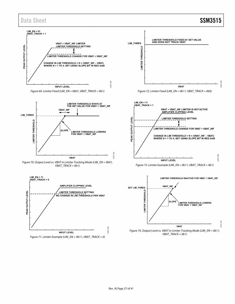
LIMITER AND BATTERY TRACKING THRESHOLD CONTROL The SSM3515 contains an output limiter that can be used limit the peak output voltage of the amplifier. The limiter works on the rms and peak value of the signal. The limiter threshold, slope, attack rate, and release rate are programmable using Register 0x07, Register 0x08, and Register 0x09. The limiter can be enabled or disabled using LIM_EN, Bits[1:0] in Register 0x07.
The threshold at which the output is limited is determined by the LIM_THRES register setting, in Register 0x08, Bits[7:3]. When the ouput signal level exceeds the set therhold level, the limiter activates and limits the signal level to the set limit. Below the set threshold, the output level is not affected. The limiter threshold can be set from 1 V peak to 15 V peak.
The limiter threshold can be set above the maximum output voltage of the amplifier. In this case, the limiter allows maximum peak output; in other words, the output may clip depending on the power supply voltage and not the limiter.
The limiter threshold can be set as fixed or to vary with the battery voltage via the VBAT_TRACK bit (Register 0x07, Bit 2). When set to fixed, the limiter threshold is fixed and does not vary with battery voltage. The threshold can be set from 1 V peak to 15 V peak using the LIM_THRES bit (see Figure 68).
When set to a variable threshold, the SSM3515 monitors the VBAT supply and automatically adjusts the limiter threshold based on the VBAT supply voltage.
The VBAT supply voltage at which the limiter threshold level begins to decrease the output level is determined by the VBAT inflection point, the VBAT_INF bits (Register 0x09, Bits[7:0]).

SSM3515 Data Sheet
Rev. A| Page 26 of 41
The VBAT_INF point is defined as the battery voltage at which the limiter either activates or deactivates depending on the LIM_EN mode (see Table 19). When the battery voltage is greater than VBAT_INF, the limiter is not active. When it battery voltage is less than VBAT_INF, the limiter is activated. The VBAT_INF bits can be set from 3.8 V to 16.2 V. The 8-bit value for the voltage can be calculated using the following equation.
Voltage = 3.8 + 12.4 × Decimal Value/255
Convert the decimal value to an 8-bit hex value and use it to set the VBAT_INF bits.
The rate at which the limiter threshold is lowered relative to the amount change in VBAT below the VBAT_INF point is determined by the slope bits (Register 0x08, Bits[1:0]).
The slope is the ratio of the limiter threshold reduction to the VBAT voltage reduction.
Slope = ΔLimiter Threshold/ΔVBAT
The slope ratio can be set from 1:1 to 4:1. This function is useful to prevent early shutdown under low battery conditions. As the VBAT voltage falls, the limiter threshold is lowered. This results in the lower output level and therefore helps to reduce the current drawn from the battery and in turn helps prevent early shutdown due to low VBAT.
The limiter offers various active modes which can be set using the LIM_EN bits (Register 0x07, Bits[1:0]) and the VBAT_TRACK bit, as shown in Table 19.
When LIM_EN = 01, the limiter is enabled. When LIM_EN = 10, the limiter mutes the output if VBAT falls below VBAT_INF. When LIM_EN = 11, the limiter engages only when the battery voltage is lower than VBAT_INF. When VBAT is above VBAT_INF, no limiting occurs. Note that there is hysteresis on VBAT_INF for the limiter disengaging.
The limiter, when active, reduces the gain of the amplifier. The rate of gain reduction or attack rate is determined by the LIM_ATR bits (Register 0x07, Bits[5:4]). Similarly, when the signal level drops below the limiter threshold, the gain is restored. The gain release rate is determined by the LIM_RRT bits (Register 0x07, Bits[7:6]).
INPUT LEVEL
PE
AK
OU
TP
UT
LE
VE
L
AMPLIFIER CLIPPING LEVEL
LIM_EN = 00VBAT_TRACK = 0
1332
7-07
8
Figure 67. Limiter Example (LIM_EN = 0b0, VBAT_TRACK = 0bx)
VBAT
LIM_THRESL
IMIT
ER
TH
RE
SH
OL
D
LIMITER THRESHOLD FIXED AT SET VALUEAND DOES NOT TRACK VBAT
1332
7-08
0
Figure 68. Limiter Fixed (LIM_EN = 0b01, VBAT_TRACK = 0b0)
Table 19. Limiter Modes LIM_EN VBAT_TRACK Limiter VBAT < VBAT_INF VBAT > VBAT_INF Comments 00 0/1 No Not applicable Not applicable See Figure 67 01 0 Fixed Use the set threshold Use the set threshold See Figure 68 01 1 Variable Lowers the threshold Use the set threshold See Figure 69 and Figure 70 10 0/1 Fixed Mutes the output Use the set threshold 11 0 Fixed Use the set threshold No limiting See Figure 71 and Figure 72 11 1 Variable Lowers the threshold No limiting See Figure 73 and Figure 74
Data Sheet SSM3515
Rev. A| Page 27 of 41
INPUT LEVEL
LIMITER THRESHOLD SETTING
PE
AK
OU
TP
UT
LE
VE
L
VBAT > VBAT_INF LIMITER
LIMITER THRESHOLD CHANGE FOR VBAT < VBAT_INF
CHANGE IN LIM THRESHOLD = N × (VBAT_INF – VBAT)WHERE N = 1 TO 4, SET USING SLOPE BIT IN REG 0x08
LIM_EN = 01VBAT_TRACK = 1
1332
7-08
1
Figure 69. Limiter Fixed (LIM_EN = 0b01, VBAT_TRACK = 0b1)
VBAT
VBAT_INF
LIM_THRES
SLOPELIMITER THRESHOLD LOWERSFOR VBAT < VBAT_INF
LIMITER THRESHOLD STAYS ATTHE SET VALUE FOR VBAT > VBAT_INF
LIM
ITE
R T
HR
ES
HO
LD
1332
7-18
1
Figure 70. Output Level vs. VBAT in Limiter Tracking Mode (LIM_EN = 0b01,
VBAT_TRACK = 0b1)
INPUT LEVEL
LIMITER THRESHOLD SETTING
PE
AK
OU
TP
UT
LE
VE
L
NO CHANGE IN LIM THRESHOLD PER VBAT
AMPLIFIER CLIPPING LEVEL
LIM_EN = 11VBAT_TRACK = 0
1332
7-08
2
Figure 71. Limiter Example (LIM_EN = 0b11, VBAT_TRACK = 0)
VBAT
LIM_THRES
LIM
ITE
R T
HR
ES
HO
LD
LIMITER THRESHOLD FIXED AT SET VALUEAND DOES NOT TRACK VBAT
1332
7-18
2
Figure 72. Limiter Fixed (LIM_EN = 0b11, VBAT_TRACK = 0b0)
INPUT LEVEL
LIMITER THRESHOLD SETTING
PE
AK
OU
TP
UT
LE
VE
L
VBAT > VBAT_INF LIMITER IS NOTACTIVE
LIMITER THRESHOLD CHANGE FOR VBAT < VBAT_INF
CHANGE IN LIM THRESHOLD = N × (VBAT_INF – VBAT)WHERE N = 1 TO 4, SET USING SLOPE BIT IN REG 0x08
AMPLIFIER CLIPPING LEVEL
LIM_EN = 11VBAT_TRACK = 1
1332
7-08
3
Figure 73. Limiter Example (LIM_EN = 0b11, VBAT_TRACK = 0b1)
VBAT
VBAT_INFSET LIM_THRES
SLOPELIMITER THRESHOLD LOWERSFOR VBAT < VBAT_INF
LIMITER THRESHOLD INACTIVE FOR VBAT > VBAT_INF
LIM
ITE
R T
HR
ES
HO
LD
1332
7-18
3
Figure 74. Output Level vs. VBAT in Limiter Tracking Mode (LIM_EN = 0b11,
VBAT_TRACK = 0b1)

SSM3515 Data Sheet
Rev. A| Page 28 of 41
LAYOUT As output power increases, care must be taken to lay out PCB traces and wires properly among the amplifier, load, and power supply; a poor layout increases voltage drops, consequently decreasing efficiency. A good practice is to use short, wide PCB tracks to decrease voltage drops and minimize inductance. For lowest dc resistance (DCR) and minimum inductance, ensure that track widths are at least 200 mil for every inch of length and use 1 oz or 2 oz copper. Use large traces for the power supply inputs and amplifier outputs. Proper grounding guidelines improve audio performance, minimize crosstalk between channels, and prevent switching noise from coupling into the audio signal.
To maintain high output swing and high peak output power, the PCB traces that connect the output pins to the load and supply pins must be as wide as possible to maintain the minimum trace resistances. It is also recommended that a large ground plane be used for minimum impedances. In addition, good PCB layout isolates critical analog paths from sources of high interference. Separate high frequency circuits (analog and digital) from low frequency circuits.
Properly designed multilayer PCBs can reduce EMI emission and increase immunity to the RF field by a factor of 10 or more, compared with double-sided boards. A multilayer board allows a complete layer to be used for the ground plane, whereas the ground plane side of a double-sided board is often disrupted by signal crossover.
If the system has separate analog and digital ground and power planes, the analog ground plane must be directly beneath the analog power plane, and, similarly, the digital ground plane must be directly beneath the digital power plane. There must be no overlap between analog and digital ground planes or between analog and digital power planes.
BOOTSTRAP CAPACITORS The output stage of the SSM3515 uses a high-side NMOS driver, rather than PMOS. Therefore, a bootstrap supply is needed to drive the high-side NMOS. To generate the boosted gate driver voltage for the high-side NMOS, a 0.22 μF bootstrap capacitor is used from each output pin to BST± pins. This capacitor boosts the voltage at BST± pins when the high-side NMOS turns on and acts as a floating power supply for that particular switching cycle. The bootstrap capacitor is charged during the low-side NMOS active period.
POWER SUPPLY DECOUPLING To ensure high efficiency, low total harmonic distortion (THD), and high power supply rejection ratio (PSRR), proper power supply decoupling is necessary. Noise transients on the power supply lines are short duration voltage spikes. These spikes can contain frequency components that extend into the hundreds of megahertz. The power supply input must be decoupled with a good quality, low ESL, low ESR bulk capacitor larger than 220 µF. This capacitor bypasses low frequency noises to the ground plane.
For high frequency transient noises, place 1 µF capacitors as close as possible to the PVDD pins of the device.

Data Sheet SSM3515
Rev. A| Page 29 of 41
REGISTER SUMMARY Table 20. Register Summary Reg. Name Bits Bit 7 Bit 6 Bit 5 Bit 4 Bit 3 Bit 2 Bit 1 Bit 0 Reset RW
0x00 Power Control [7:0] APWDN_ EN
BSNS_ PWDN
RESERVED S_RST SPWDN 0x81 R/W
0x01 Gain and Edge Control
[7:0] RESERVED EDGE RESERVED ANA_GAIN 0x01 R/W
0x02 DAC Control [7:0] DAC_HV DAC_MUTE DAC_HPF DAC_LPM RESERVED DAC_FS 0x32 R/W
0x03 DAC Volume Control
[7:0] VOL 0x40 R/W
0x04 SAI Control 1 [7:0] DAC_POL BCLK_POL TDM_BCLKS FSYNC_ MODE
SDATA_ FMT
SAI_MODE 0x11 R/W
0x05 SAI Control 2 [7:0] DATA_ WIDTH
RESERVED AUTO_ SLOT
TDM_SLOT 0x00 R/W
0x06 Battery Voltage Output
[7:0] VBAT 0x00 R
0x07 Limiter Control 1 [7:0] LIM_RRT LIM_ATR RESERVED VBAT_ TRACK
LIM_EN 0xA4 R/W
0x08 Limiter Control 2 [7:0] LIM_THRES RESERVED SLOPE 0x51 R/W
0x09 Limiter Control 3 [7:0] VBAT_INF 0x22 R/W
0x0A Status [7:0] RESERVED UVLO_VREG LIM_EG CLIP AMP_OC OTF OTW BAT_WARN 0x00 R
0x0B Fault Control [7:0] OTW_GAIN MRCV MAX_AR ARCV_UV ARCV_OT ARCV_OC 0x18 R/W

SSM3515 Data Sheet
Rev. A| Page 30 of 41
REGISTER DETAILS POWER CONTROL REGISTER Address: 0x00, Reset: 0x81, Name: Power Control
Table 21. Bit Descriptions for Power Control Bits Bit Name Settings Description Reset Access
7 APWDN_EN Auto Power-Down Enable. Auto power-down automatically puts the IC in a low power state when 2048 consecutive zero input samples have been received.
0x1 R/W
0 Auto Power-Down Disabled.
1 Auto Power-Down Enabled. When APWDN_EN = 1 the device automatically powers down when 2048 consecutive zero value input samples have been received. The device automatically powers up when a single nonzero sample is received.
6 BSNS_PWDN Battery Voltage Sense Power-Down. 0x0 R/W
0 Battery Voltage Sense Powered On.
1 Battery Voltage Sense Powered Off.
[5:2] RESERVED Reserved. 0x0 R/W
1 S_RST Full Software Reset. 0x0 W
0 Normal Operation.
1 Reset all Blocks and I2C Registers.
0 SPWDN Master Software Power-Down. Software power-down puts all blocks except the I2C interface in a low-power state.
0x1 R/W
0 Normal Operation.
1 Software Master Power-Down.
GAIN AND EDGE CONTROL REGISTER Address: 0x01, Reset: 0x01, Name: Gain and Edge Control
Table 22. Bit Descriptions for Gain and Edge Control Bits Bit Name Settings Description Reset Access
[7:5] RESERVED Reserved. 0x0 R/W
7 0
6 0
5 0
4 0
3 0
2 0
1 0
0 1
[7:5] RESERVED [1:0] ANA_GAIN (R/W) Amp Analog Gain Selection
00: 8.4V Full-Scale Gain Mapping. 01: 12.6V Full-Scale Gain Mapping. 10: 14V Full-Scale Gain Mapping. 11: 15V Full-Scale Gain Mapping.
[4] EDGE (R/W) Edge Rate Control
0: Normal Operation. 1: Low EMI Mode Operation.
[3:2] RESERVED
7 1
6 0
5 0
4 0
3 0
2 0
1 0
0 1
[7] APW DN_EN (R/W) Auto Power-Down Enable
0: Auto Power-Down Disabled. 1: Auto Power-Down Enabled.
[0] SPW DN (R/W) Master Software Power-Down
0: Normal Operation. 1: Software Master Power-Down.
[6] BSNS_PWDN (R/W) Battery Voltage Sense Power-Down
0: Battery Voltage Sense Powered On. 1: Battery Voltage Sense Powered Off.
[1] S_RST (W) Full Software Reset
0: Normal Operation. 1: Reset all blocks and I2C registers.
[5:2] RESERVED
Data Sheet SSM3515
Rev. A| Page 31 of 41
Bits Bit Name Settings Description Reset Access
4 EDGE Edge Rate Control. This controls the edge speed of the power stage. The low EMI operation mode reduces the edge speed, lowering EMI and power efficiency
0x0 R/W
0 Normal Operation.
1 Low EMI Mode Operation.
[3:2] RESERVED Reserved. 0x0 R/W
[1:0] ANA_GAIN Amp Analog Gain Selection. 0x1 R/W
00 8.4 V Full-Scale Gain Mapping.
01 12.6 V Full-Scale Gain Mapping.
10 14 V Full-Scale Gain Mapping.
11 15 V Full-Scale Gain Mapping.
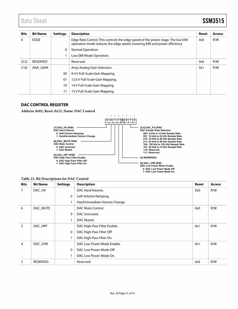
DAC CONTROL REGISTER Address: 0x02, Reset: 0x32, Name: DAC Control
Table 23. Bit Descriptions for DAC Control Bits Bit Name Settings Description Reset Access
7 DAC_HV DAC Hard Volume. 0x0 R/W
0 Soft Volume Ramping.
1 Hard/Immediate Volume Change.
6 DAC_MUTE DAC Mute Control. 0x0 R/W
0 DAC Unmuted.
1 DAC Muted.
5 DAC_HPF DAC High-Pass Filter Enable. 0x1 R/W
0 DAC High-Pass Filter Off.
1 DAC High-Pass Filter On.
4 DAC_LPM DAC Low Power Mode Enable. 0x1 R/W
0 DAC Low Power Mode Off.
1 DAC Low Power Mode On.
3 RESERVED Reserved. 0x0 R/W
7
0
6
0
5
1
4
1
3
0
2
0
1
1
0
0
[7] DAC_HV (R/W) DAC Hard Volume
0: Soft Volume Ramping. 1: Hard/Immediate Volume Change.
[2:0] DAC_FS (R/W)DAC Sample Rate Selection
000: 8 kHz to 12 kHz Sample Rate. 001: 16 kHz to 24 kHz Sample Rate. 010: 32 kHz to 48 kHz Sample Rate. 011: 64 kHz to 96 kHz Sample Rate. 100: 128 kHz to 192 kHz Sample Rate. 101: 48 kHz to 72 kHz Sample Rate. 110: Reserved.111: Reserved.
[6] DAC_MUTE (R/W) DAC Mute Control
0: DAC Unmuted. 1: DAC Muted.
[5] DAC_HPF (R/W) DAC High Pass Filter Enable
0: DAC High Pass Filter Off. 1: DAC High Pass Filter On.
[3] RESERVED
[4] DAC_LPM (R/W)DAC Low Power Mode Enable
0: DAC Low Power Mode Off. 1: DAC Low Power Mode On.
SSM3515 Data Sheet
Rev. A| Page 32 of 41
Bits Bit Name Settings Description Reset Access
[2:0] DAC_FS DAC Sample Rate Selection. 0x2 R/W
000 8 kHz to 12 kHz Sample Rate.
001 16 kHz to 24 kHz Sample Rate.
010 32 kHz to 48 kHz Sample Rate.
011 64 kHz to 96 kHz Sample Rate.
100 128 kHz to 192 kHz Sample Rate.
101 48 kHz to 72 kHz Sample Rate.
110 Reserved.
111 Reserved.
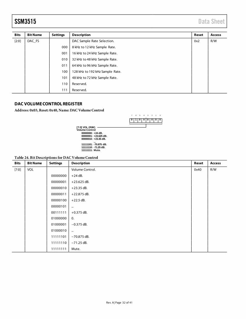
DAC VOLUME CONTROL REGISTER Address: 0x03, Reset: 0x40, Name: DAC Volume Control
Table 24. Bit Descriptions for DAC Volume Control Bits Bit Name Settings Description Reset Access
[7:0] VOL Volume Control. 0x40 R/W
00000000 +24 dB.
00000001 +23.625 dB.
00000010 +23.35 dB.
00000011 +22.875 dB.
00000100 +22.5 dB.
00000101 ...
00111111 +0.375 dB.
01000000 0.
01000001 −0.375 dB.
01000010 ...
11111101 −70.875 dB.
11111110 −71.25 dB.
11111111 Mute.
7 0
6 1
5 0
4 0
3 0
2 0
1 0
0 0
[7:0] VOL (R/W) Volume Control
00000000: +24 dB. 00000001: +23.625 dB. 00000010: +23.35 dB.
... 11111101: -70.875 dB. 11111110: -71.25 dB. 11111111: Mute.
Data Sheet SSM3515
Rev. A| Page 33 of 41
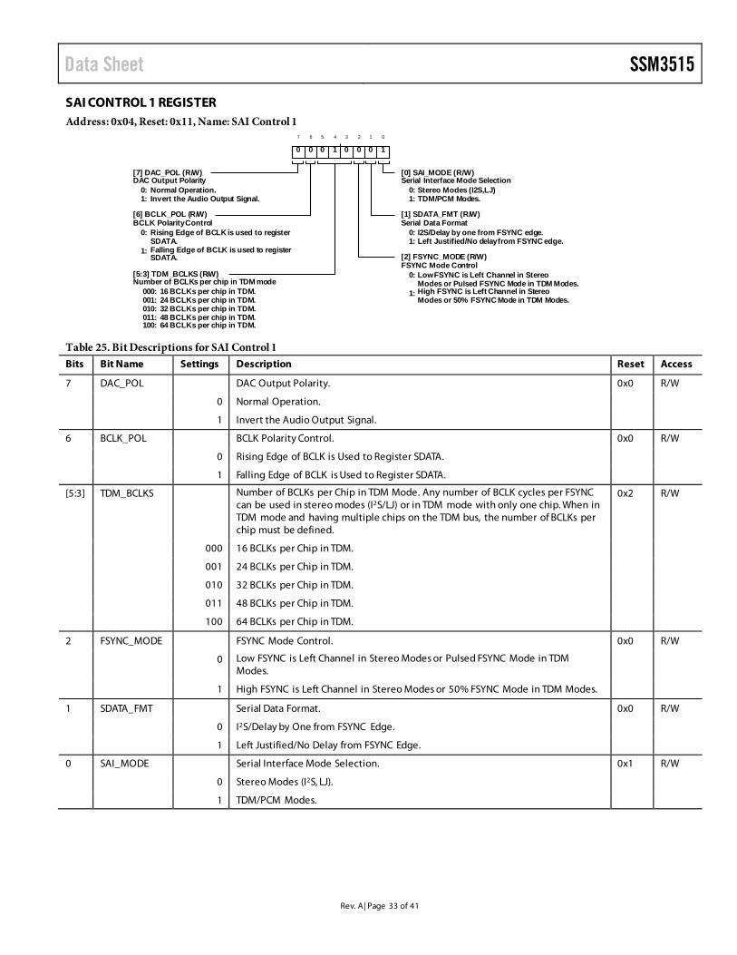
SAI CONTROL 1 REGISTER Address: 0x04, Reset: 0x11, Name: SAI Control 1
Table 25. Bit Descriptions for SAI Control 1 Bits Bit Name Settings Description Reset Access
7 DAC_POL DAC Output Polarity. 0x0 R/W
0 Normal Operation.
1 Invert the Audio Output Signal.
6 BCLK_POL BCLK Polarity Control. 0x0 R/W
0 Rising Edge of BCLK is Used to Register SDATA.
1 Falling Edge of BCLK is Used to Register SDATA.
[5:3] TDM_BCLKS Number of BCLKs per Chip in TDM Mode. Any number of BCLK cycles per FSYNC can be used in stereo modes (I2S/LJ) or in TDM mode with only one chip. When in TDM mode and having multiple chips on the TDM bus, the number of BCLKs per chip must be defined.
0x2 R/W
000 16 BCLKs per Chip in TDM.
001 24 BCLKs per Chip in TDM.
010 32 BCLKs per Chip in TDM.
011 48 BCLKs per Chip in TDM.
100 64 BCLKs per Chip in TDM.
2 FSYNC_MODE FSYNC Mode Control. 0x0 R/W
0 Low FSYNC is Left Channel in Stereo Modes or Pulsed FSYNC Mode in TDM Modes.
1 High FSYNC is Left Channel in Stereo Modes or 50% FSYNC Mode in TDM Modes.
1 SDATA_FMT Serial Data Format. 0x0 R/W
0 I2S/Delay by One from FSYNC Edge.
1 Left Justified/No Delay from FSYNC Edge.
0 SAI_MODE Serial Interface Mode Selection. 0x1 R/W
0 Stereo Modes (I2S, LJ).
1 TDM/PCM Modes.
7 0
6 0
5 0
4 1
3 0
2 0
1 0
0 1
[7] DAC_POL (R/W) DAC Output Polarity
0: Normal Operation. 1: Invert the Audio Output Signal.
[0] SAI_MODE (R/W) Serial Interface Mode Selection
0: Stereo Modes (I2S,LJ) 1: TDM/PCM Modes.
[6] BCLK_POL (R/W) BCLK Polarity Control
0: Rising Edge of BCLK is used to register SDATA.
1: Falling Edge of BCLK is used to register SDATA.
[1] SDATA_FMT (R/W) Serial Data Format
0: I2S/Delay by one from FSYNC edge. 1: Left Justified/No delay from FSYNC edge.
[2] FSYNC_MODE (R/W) FSYNC Mode Control
0: Low FSYNC is Left Channel in Stereo Modes or Pulsed FSYNC Mode in TDM Modes.
1: High FSYNC is Left Channel in Stereo Modes or 50% FSYNC Mode in TDM Modes.
[5:3] TDM_BCLKS (R/W) Number of BCLKs per chip in TDM mode
000: 16 BCLKs per chip in TDM. 001: 24 BCLKs per chip in TDM. 010: 32 BCLKs per chip in TDM. 011: 48 BCLKs per chip in TDM. 100: 64 BCLKs per chip in TDM.

SSM3515 Data Sheet
Rev. A| Page 34 of 41
SAI CONTROL 2 REGISTER Address: 0x05, Reset: 0x00, Name: SAI Control 2
Table 26. Bit Descriptions for SAI Control 2 Bits Bit Name Settings Description Reset Access
7 DATA_WIDTH Audio Data Width. 0x0 R/W
0 Audio Input on SDATA is 24 Bits.
1 Audio Input on SDATA is 16 Bits.
[6:5] RESERVED Reserved. 0x0 R/W
4 AUTO_SLOT Automatic TDM Slot Selection. 0x0 R/W
0 TDM Slot Determined by the TDM_SLOT Register.
1 TDM Slot Determined by the ADDR Pin.
[3:0] TDM_SLOT TDM Slot Selection. 0x0 R/W
0000 Chip Slot 1 Used.
0001 Chip Slot 2 Used.
0010 Chip Slot 3 Used.
0011 Chip Slot 4 Used.
0100 Chip Slot 5 Used.
0101 Chip Slot 6 Used.
0110 Chip Slot 7 Used.
0111 Chip Slot 8 Used.
1000 Chip Slot 9 Used.
1001 Chip Slot 10 Used.
1010 Chip Slot 11 Used.
1011 Chip Slot 12 Used.
1100 Chip Slot 13 Used.
1101 Chip Slot 14 Used.
1110 Chip Slot 15 Used.
1111 Chip Slot 16 Used.
7 0
6 0
5 0
4 0
3 0
2 0
1 0
0 0
[7] DATA_W IDTH (R/W) Audio Data W idth
0: Audio input on SDATA is 24 bits. 1: Audio input on SDATA is 16 bits.
[3:0] TDM_SLOT (R/W) TDM Slot Selection
0000: Chip Slot 1 Used. 0001: Chip Slot 2 Used. 0010: Chip Slot 3 Used.
... 1101: Chip Slot 14 Used. 1110: Chip Slot 15 Used. 1111: Chip Slot 16 Used.
[6:5] RESERVED [4] AUTO_SLOT (R/W) Automatic TDM Slot Selection
0: TDM Slot determined by TDM_SLOT register. 1: TDM Slot determined by ADDR pin.

Data Sheet SSM3515
Rev. A| Page 35 of 41
BATTERY VOLTAGE OUTPUT REGISTER Address: 0x06, Reset: 0x00, Name: Battery Voltage Output
Table 27. Bit Descriptions for Battery Voltage Output Bits Bit Name Settings Description Reset Access
[7:0] VBAT 8-Bit Unsigned Battery Voltage 0x0 R
LIMITER CONTROL 1 REGISTER Address: 0x07, Reset: 0xA4, Name: Limiter Control 1
Table 28. Bit Descriptions for Limiter Control 1 Bits Bit Name Settings Description Reset Access
[7:6] LIM_RRT Limiter Release Rate. 0x2 R/W
00 3200 ms/dB.
01 1600 ms/dB.
10 1200 ms/dB.
11 800 ms/dB.
[5:4] LIM_ATR Limiter Attack Rate. 0x2 R/W
00 120 µs/dB.
01 60 µs/dB.
10 30 µs/dB.
11 20 µs/dB.
3 RESERVED Reserved. 0x0 R/W
2 VBAT_TRACK Threshold Battery Tracking Enable. 0x1 R/W
0 Limiter Attack Threshold Fixed.
1 Limiter Attack Threshold Varies or Gain Reduction with Battery Voltage.
[1:0] LIM_EN Limiter or Mute Mode Enable. 0x0 R/W
00 Limiter and Mute Mode Off.
01 Limiter On.
10 Output Mutes if VBAT is Below VBAT_INF.
11 Limiter On But Only Engages if VBAT is Below VBAT_INF.
7 1
6 0
5 1
4 0
3 0
2 1
1 0
0 0
[7:6] LIM_RRT (R/W) Limiter Release Rate
00: 3200 ms/dB. 01: 1600 ms/dB. 10: 1200 ms/dB. 11: 800 ms/dB.
[1:0] LIM_EN (R/W) Limiter or Mute Mode Enable
00: Limiter and Mute Mode Off. 01: Limiter On. 10: Output mutes if VBAT is below VBAT_INF. 11: Limiter On but only engages if VBAT
is below VBAT_INF. [5:4] LIM_ATR (R/W) Limiter Attack Rate
00: 120 us/dB. 01: 60 us/dB. 10: 30 us/dB. 11: 20 us/dB.
[2] VBAT_TRACK (R/W) Threshold Battery Tracking Enable
0: Limiter Attack Threshold Fixed. 1: Limiter Attack Threshold Varies or gain
reduction with Battery Voltage. [3] RESERVED
7 0
6 0
5 0
4 0
3 0
2 0
1 0
0 0
[7:0] VBAT (R) 8-Bit Unsigned Battery Voltage

SSM3515 Data Sheet
Rev. A| Page 36 of 41
LIMITER CONTROL 2 REGISTER Address: 0x08, Reset: 0x51, Name: Limiter Control 2
Table 29. Bit Descriptions for Limiter Control 2 Bits Bit Name Settings Description Reset Access
[7:3] LIM_THRES Limiter Attack Threshold. 0xA R/W
00000 15.0 V peak Output.
00001 14.5 V peak Output.
00010 14.0 V peak Output.
00011 13.5 V peak Output.
00100 13.0 V peak Output.
00101 12.5 V peak Output.
00110 12.0 V peak Output.
00111 11.5 V peak Output.
01000 11.0 V peak Output.
01001 10.5 V peak Output.
01010 10.0 V peak Output.
01011 9.5 V peak Output.
01100 9.0 V peak Output.
01101 8.5 V peak Output.
01110 8.25 V peak Output.
01111 8.0 V peak Output.
10000 7.75 V peak Output.
10001 7.5 V peak Output.
10010 7.25 V peak Output.
10011 7.0 V peak Output.
10100 6.5 V peak Output.
10101 6.0 V peak Output.
10110 5.5 V peak Output.
10111 5.0 V peak Output.
11000 4.5 V peak Output.
11001 4.0 V peak Output.
11010 3.5 V peak Output.
11011 3.0 V peak Output.
11100 2.5 V peak Output.
11101 2.0 V peak Output.
11110 1.5 V peak Output.
11111 1.0 V peak Output.
7 0
6 1
5 0
4 1
3 0
2 0
1 0
0 1
[7:3] LIM_THRES (R/W) Limiter Attack Threshold
00000: 15.0 V peak Output. 00001: 14.5 V peak Output. 00010: 14.0 V peak Output.
... 11101: 2.0 V peak Output. 11110: 1.5V V peak Output. 11111: 1.0 V peak Output.
[1:0] SLOPE (R/W) Slope of threshold reduction/battery voltage change
00: 1:1 Threshold/Battery Reduction. 01: 2:1 Threshold/Battery Reduction. 10: 3:1 Threshold/Battery Reduction. 11: 4:1 Threshold/Battery Reduction.
[2] RESERVED

Data Sheet SSM3515
Rev. A| Page 37 of 41
Bits Bit Name Settings Description Reset Access
2 RESERVED Reserved. 0x0 R/W
[1:0] SLOPE Slope of Threshold Reduction/Battery Voltage Change. 0x1 R/W
00 1:1 Threshold/Battery Reduction.
01 2:1 Threshold/Battery Reduction.
10 3:1 Threshold/Battery Reduction.
11 4:1 Threshold/Battery Reduction.
LIMITER CONTROL 3 REGISTER Address: 0x09, Reset: 0x22, Name: Limiter Control 3
Table 30. Bit Descriptions for Limiter Control 3 Bits Bit Name Settings Description Reset Access
[7:0] VBAT_INF Battery Voltage Inflection Point. This is the VBAT sense value at which the limiter either activates or starts reducing the threshold. It corresponds to the value that can be read in the VBAT read only status register. To calculate this value in volts, refer to the VBAT Sensing section. Voltage = 3.8 + 12.4 × Decimal Value/255.
0x22 R/W
STATUS REGISTER Address: 0x0A, Reset: 0x00, Name: Status
Table 31. Bit Descriptions for Status Bits Bit Name Settings Description Reset Access
7 RESERVED Reserved. 0x0 R
6 UVLO_VREG Regulator Undervoltage Fault Status. 0x0 R
0 Normal Operation.
1 Voltage Regulator Fault Condition.
5 LIM_EG Limiter/Gain Reduction Engaged. 0x0 R
0 Normal Operation.
1 Limiter or Gain Reduction has Reduced Gain.
7 0
6 0
5 0
4 0
3 0
2 0
1 0
0 0
[7] RESERVED [0] BAT_W ARN (R) Battery Voltage W arning
0: Battery Voltage above VBAT_INF. 1: Battery Voltage at or below VBAT_INF.
[6] UVLO_VREG (R) Regulator Undervoltage Fault Status
0: Normal Operation. 1: Voltage Regulator Fault Condition. [1] OTW (R)
Over Temperature Warning Status 0: Normal Operation. 1: Over Temperature Warning Condition.
[5] LIM_EG (R) Limiter/Gain Reduction Engaged
0: Normal Operation. 1: Limiter or Gain Reduction has Reduced
Gain. [2] OTF (R) Over Temperature Fault Status
0: Normal Operation. 1: Over Temperature Fault Condition. [4] CLIP (R)
Clip Detector 0: Normal Operation. 1: Amplifier Clipping Detected.
[3] AMP_OC (R) Amplifier Over-Current Fault Status
0: Normal Operation. 1: Amp Over-Current Fault Condition.
7 0
6 0
5 1
4 0
3 0
2 0
1 1
0 0
[7:0] VBAT_INF (R/W) Battery Voltage Inflection Point

SSM3515 Data Sheet
Rev. A| Page 38 of 41
Bits Bit Name Settings Description Reset Access
4 CLIP Clip Detector. 0x0 R
0 Normal Operation.
1 Amplifier Clipping Detected.
3 AMP_OC Amplifier Overcurrent Fault Status. 0x0 R
0 Normal Operation.
1 Amp Over-Current Fault Condition.
2 OTF Overtemperature Fault Status. 0x0 R
0 Normal Operation.
1 Overtemperature Fault Condition.
1 OTW Overtemperature Warning Status. 0x0 R
0 Normal Operation.
1 Overtemperature Warning Condition.
0 BAT_WARN Battery Voltage Warning. 0x0 R
0 Battery Voltage Above VBAT_INF.
1 Battery Voltage at or Below VBAT_INF.
FAULT CONTROL REGISTER Address: 0x0B, Reset: 0x18, Name: Fault Control
Table 32. Bit Descriptions for Fault Control Bits Bit Name Settings Description Reset Access
[7:6] OTW_GAIN Over Thermal Warning Gain Reduction. 0x0 R/W
00 No Gain Reduction in Thermal Warning.
01 1.5 dB Gain Reduction in Thermal Warning.
10 3 dB Gain Reduction in Thermal Warning.
11 5.625 dB Gain Reduction in Thermal Warning.
5 MRCV Manual Fault Recovery. 0x0 W
0 Normal Operation.
1 Writing of 1 Causes a Manual Fault Recovery Attempt when ARCV = 11.
7 0
6 0
5 0
4 1
3 1
2 0
1 0
0 0
[7:6] OTW_GAIN (R/W) Over Thermal W arning Gain Reduction
00: No gain reduction in thermal warning. 01: 1.5dB gain reduction in thermal warning. 10: 3dB gain reduction in thermal warning. 11: 5.625dB gain reduction in thermal warning.
[0] ARCV_OC (R/W) Over Current Automatic Fault Recovery Control
0: Automatic Fault Recovery for Over-Current Fault.
1: Manual Fault Recovery for Over-Current Fault.
[5] MRCV (W) Manual Fault Recovery
0: Normal Operation. 1: W riting of 1 causes a manual fault
recovery attempt when ARCV=11.
[1] ARCV_OT (R/W) Overtemperature Automatic Fault Recovery Control
0: Automatic Fault Recovery for Overtemperature Fault.
1: Manual Fault Recovery for Overtemperature Fault.
[4:3] MAX_AR (R/W) Maximum Fault recovery Attempts
00: 1 Auto Recovery Attempt. 01: 3 Auto Recovery Attempts. 10: 7 Auto Recovery Attempts. 11: Unlimited Auto Recovery Attempts.
[2] ARCV_UV (R/W) Undervoltage Automatic Fault Recovery Control
0: Automatic Fault Recovery for Undervoltage Fault.
1: Manual Fault Recovery for Undervoltage Fault.

Data Sheet SSM3515
Rev. A| Page 39 of 41
Bits Bit Name Settings Description Reset Access
[4:3] MAX_AR Maximum Fault Recovery Attempts. The maximum autorecovery register determines how many attempts at autorecovery are performed.
0x3 R/W
00 1 Autorecovery Attempt.
01 3 Autorecovery Attempts.
10 7 Autorecovery Attempts.
11 Unlimited Autorecovery Attempts.
2 ARCV_UV Undervoltage Automatic Fault Recovery Control. 0x0 R/W
0 Automatic Fault Recovery for Undervoltage Fault.
1 Manual Fault Recovery for Undervoltage Fault.
1 ARCV_OT Overtemperature Automatic Fault Recovery Control. 0x0 R/W
0 Automatic Fault Recovery for Overtemperature Fault.
1 Manual Fault Recovery for Overtemperature Fault.
0 ARCV_OC Overcurrent Automatic Fault Recovery Control. 0x0 R/W
0 Automatic Fault Recovery for Overcurrent Fault.
1 Manual Fault Recovery for Overcurrent Fault.

SSM3515 Data Sheet
Rev. A| Page 40 of 41
TYPICAL APPLICATION CIRCUIT Figure 75 shows a typical application circuit for a single channel output.
BCLK
FSYNC
SDATA
OUT+
OUT–
VREG50/AVDD
+5V (AVDD)
VREG18/DVDD
AGND
REG_EN PVDD
PGND
SCL
SDA
ADDR
I2CI2C
TDMI2S
INPUTVOLUME DAC
FULLBRIDGEPOWERSTAGE
Σ-∆CLASS-D
MODULATOR
BST–
BST+
SSM3515
+1.8V (DVDD)+1.8V
I2S/TDM
SEE THE ADDR PIN SETUP AND CONTROL SECTION
PVDD
R12.2kΩ
R22.2kΩ
R3
R4
C12.2µF
C31µF
C50.22µF
C60.22µF
C8220pF
C7220pF
+4.5V TO +17VPVDD
4Ω/8Ω
FB1
FB2
OPTIONAL
FB1/FB2: MURATA FERRITE BEAD NFZ2MSM181
C6470µF
C510µF
C40.1µF
REGDVDD
REGAVDD
PVDD
REG_ENR3 0Ω EXTERNAL DVDDR4 0Ω INTERNAL DVDD
C20.1uF
1332
7-18
4
Figure 75. Typical Application Circuit for Single Channel Output

Data Sheet SSM3515
Rev. A| Page 41 of 41
OUTLINE DIMENSIONS
A
B
C
D
E
2.2402.2002.160
1.8401.8001.760
1234
BOTTOM VIEW(BALL SIDE UP)
TOP VIEW(BALL SIDE DOWN)
BALL A1IDENTIFIER
0.40BSC
0.5600.5000.440
SIDE VIEW
0.2300.2000.170
0.3000.2600.220
1.60 REF
1.20 REF
COPLANARITY0.05
SEATINGPLANE
12-1
9-20
12-
A
Figure 76. 20-Ball Wafer Level Chip Scale Package [WLCSP]
(CB-20-10) Dimensions shown in millimeters
ORDERING GUIDE Model1 Temperature Range Package Description Package Option SSM3515CCBZ-RL −40°C to +85°C 20-Ball Wafer Level Chip Scale Package [WLCSP] CB-20-10 SSM3515CCBZ-R7 −40°C to +85°C 20-Ball Wafer Level Chip Scale Package [WLCSP] CB-20-10
EVAL-SSM3515Z Evaluation Board
1 Z = RoHS Compliant Part.
I2C refers to a communications protocol originally developed by Philips Semiconductors (now NXP Semiconductors).
©2015–2017 Analog Devices, Inc. All rights reserved. Trademarks and registered trademarks are the property of their respective owners. D13327-0-1/17(A)