Embed Size (px)
Citation preview
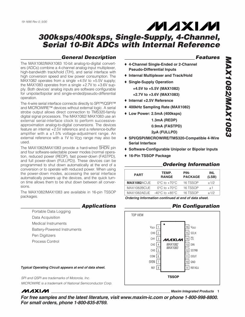
General DescriptionThe MAX1082/MAX1083 10-bit analog-to-digital convert-ers (ADCs) combine a 4-channel analog-input multiplexer,high-bandwidth track/hold (T/H), and serial interface withhigh conversion speed and low power consumption. TheMAX1082 operates from a single +4.5V to +5.5V supply;the MAX1083 operates from a single +2.7V to +3.6V sup-ply. Both devices’ analog inputs are software configurablefor unipolar/bipolar and single-ended/pseudo-differentialoperation.
The 4-wire serial interface connects directly to SPI™/QSPI™and MICROWIRE™ devices without external logic. A serialstrobe output allows direct connection to TMS320-familydigital signal processors. The MAX1082/ MAX1083 use anexternal serial-interface clock to perform successive-approximation analog-to-digital conversions. The devicesfeature an internal +2.5V reference and a reference-bufferamplifier with a ±1.5% voltage-adjustment range. Anexternal reference with a 1V to VDD range may also beused.
The MAX1082/MAX1083 provide a hard-wired SHDN pinand four software-selectable power modes (normal opera-tion, reduced power (REDP), fast power-down (FASTPD),and full power-down (FULLPD)). These devices can beprogrammed to shut down automatically at the end of aconversion or to operate with reduced power. When usingthe power-down modes, accessing the serial interfaceautomatically powers up the devices, and the quick turn-on time allows them to be shut down between all conver-sions.
The MAX1082/MAX1083 are available in 16-pin TSSOPpackages.
ApplicationsPortable Data Logging
Data Acquisition
Medical Instruments
Battery-Powered Instruments
Pen Digitizers
Process Control
Features 4-Channel Single-Ended or 2-Channel
Pseudo-Differential Inputs
Internal Multiplexer and Track/Hold
Single-Supply Operation
+4.5V to +5.5V (MAX1082)
+2.7V to +3.6V (MAX1083)
Internal +2.5V Reference
400kHz Sampling Rate (MAX1082)
Low Power: 2.5mA (400ksps)
1.3mA (REDP)
0.9mA (FASTPD)
2µA (FULLPD)
SPI/QSPI/MICROWIRE/TMS320-Compatible 4-WireSerial Interface
Software-Configurable Unipolar or Bipolar Inputs
16-Pin TSSOP Package
MA
X1
08
2/M
AX
10
83
300ksps/400ksps, Single-Supply, 4-Channel,Serial 10-Bit ADCs with Internal Reference
________________________________________________________________ Maxim Integrated Products 1
16
15
14
13
12
11
10
9
1
2
3
4
5
6
7
8
VDD1 VDD2
SCLK
CS
DIN
SSTRB
DOUT
GND
REFADJ
TOP VIEW
MAX1082MAX1083
TSSOP
CH0
CH1
COM
CH2
CH3
SHDN
REF
19-1690 Rev 0; 5/00
PART
MAX1082ACUE
MAX1082BCUE
MAX1082AEUE -40°C to +85°C
0°C to +70°C
0°C to +70°C
TEMP. RANGE
PIN-PACKAGE
16 TSSOP
16 TSSOP
16 TSSOP
Typical Operating Circuit appears at end of data sheet.
Pin Configuration
INL(LSB)
±1/2
±1
±1/2
SPI and QSPI are trademarks of Motorola, Inc.
MICROWIRE is a trademark of National Semiconductor Corp.
Ordering Information continued at end of data sheet.
Ordering Information
For free samples and the latest literature, visit www.maxim-ic.com or phone 1-800-998-8800.For small orders, phone 1-800-835-8769.
MA
X1
08
2/M
AX
10
83
300ksps/400ksps, Single-Supply, 4-Channel,Serial 10-Bit ADCs with Internal Reference
2 _______________________________________________________________________________________
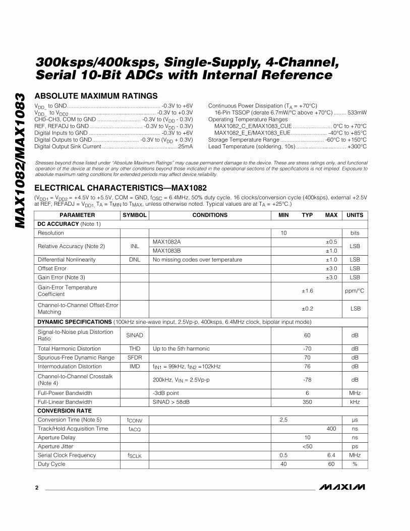
ABSOLUTE MAXIMUM RATINGS
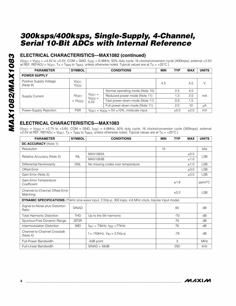
ELECTRICAL CHARACTERISTICS—MAX1082(VDD1 = VDD2 = +4.5V to +5.5V, COM = GND, fOSC = 6.4MHz, 50% duty cycle, 16 clocks/conversion cycle (400ksps), external +2.5Vat REF, REFADJ = VDD1, TA = TMIN to TMAX, unless otherwise noted. Typical values are at TA = +25°C.)
Stresses beyond those listed under “Absolute Maximum Ratings” may cause permanent damage to the device. These are stress ratings only, and functionaloperation of the device at these or any other conditions beyond those indicated in the operational sections of the specifications is not implied. Exposure toabsolute maximum rating conditions for extended periods may affect device reliability.
VDD_ to GND............................................................ -0.3V to +6VVDD_ to VDD2 ....................................................... -0.3V to +0.3VCH0–CH3, COM to GND ............................ -0.3V to (VDD - 0.3V)REF, REFADJ to GND .................................. -0.3V to VDD - 0.3V)Digital Inputs to GND .............................................. -0.3V to +6VDigital Outputs to GND.............................. -0.3V to (VDD + 0.3V)Digital Output Sink Current .................................................25mA
Continuous Power Dissipation (TA = +70°C)16-Pin TSSOP (derate 6.7mW/°C above +70°C) ........ 533mW
Operating Temperature RangesMAX1082_C_E/MAX1083_CUE ......................... 0°C to +70°CMAX1082_E_E/MAX1083_EUE....................... -40°C to +85°C
Storage Temperature Range ............................ -60°C to +150°CLead Temperature (soldering, 10s) ................................ +300°C
MAX1082A
SINAD > 58dB
-3dB point
200kHz, VIN = 2.5Vp-p
fIN1 = 99kHz, fIN2 =102kHz
MAX1083B
No missing codes over temperature
Up to the 5th harmonic
CONDITIONS
MHz0.5 6.4fSCLKSerial Clock Frequency
ps<50Aperture Jitter
ns10Aperture Delay
ns400tACQTrack/Hold Acquisition Time
µs2.5tCONVConversion Time (Note 5)
kHz350Full-Linear Bandwidth
MHz6Full-Power Bandwidth
dB-78Channel-to-Channel Crosstalk(Note 4)
dB76IMDIntermodulation Distortion
dB70SFDRSpurious-Free Dynamic Range
dB-70THDTotal Harmonic Distortion
LSB±0.5
INLRelative Accuracy (Note 2)
bits10Resolution
dB60SINADSignal-to-Noise plus DistortionRatio
LSB±0.2Channel-to-Channel Offset-ErrorMatching
ppm/°C ±1.6Gain-Error TemperatureCoefficient
±1.0
LSB±1.0DNLDifferential Nonlinearity
LSB±3.0Offset Error
LSB±3.0Gain Error (Note 3)
UNITSMIN TYP MAXSYMBOLPARAMETER
%40 60Duty Cycle
DYNAMIC SPECIFICATIONS (100kHz sine-wave input, 2.5Vp-p, 400ksps, 6.4MHz clock, bipolar input mode)
DC ACCURACY (Note 1)
CONVERSION RATE

mA
MA
X1
08
2/M
AX
10
83
300ksps/400ksps, Single-Supply, 4-Channel,Serial 10-Bit ADCs with Internal Reference
_______________________________________________________________________________________ 3
ELECTRICAL CHARACTERISTICS—MAX1082 (continued)(VDD1 = VDD2 = +4.5V to +5.5V, COM = GND, fOSC = 6.4MHz, 50% duty cycle, 16 clocks/conversion cycle (400ksps), external +2.5Vat REF, REFADJ = VDD1, TA = TMIN to TMAX, unless otherwise noted. Typical values are at TA = +25°C.)
CONDITIONS UNITSMIN TYP MAXSYMBOLPARAMETER
To power down the internal reference
For small adjustments, from 1.22V
0 to 1mA output load
On/off leakage current, VCOM VCH_ = 0 or VDD1
TA = +25°C
Bipolar, VCOM or VCH_ = VREF/2, referenced to COM or CH_
Unipolar, VCOM = 0
V/V+2.05Buffer Voltage Gain
V1.4 VDD1 - 1.0REFADJ Buffer DisableThreshold
mV±100REFADJ Input Range
V1.22REFADJ Output Voltage
µF0.01 10Capacitive Bypass at REFADJ
µF4.7 10Capacitive Bypass at REF
mV/mA0.05 2.0Load Regulation (Note 7)
ppm/°C±15TC VREFREF Output TemperatureCoefficient
mA15REF Short-Circuit Current
V2.480 2.500 2.520VREFREF Output Voltage
pF18Input Capacitance
µA±0.001 ±1Multiplexer Leakage Current
±VREF/2V
VREF
VCH_Input Voltage Range, SingleEnded and Differential (Note 6)
VIN = 0 or VDD2
In full power-down mode, fSCLK = 0
VREF = 2.500V, fSCLK = 0
VREF = 2.500V, fSCLK = fMAX
(Note 8)
pFCINInput Capacitance
µA±1IINInput Leakage
V0.2VHYSTInput Hysteresis
V0.8VINLInput Low Voltage
V3.0VINHInput High Voltage
5
320 µA
200 350
REF Input Current
V1.0 VDD1 +
50mVREF Input Voltage Range
ISINK = 5mA V0.4VOLOutput Voltage Low
15
ISOURCE = 1mA V4VOHOutput Voltage High
CS = VDD2 µA±10ILThree-State Leakage Current
CS = VDD2 pF15COUTThree-State Output Capacitance
ANALOG INPUTS (CH3–CH0, COM)
EXTERNAL REFERENCE (reference buffer disabled, reference applied to REF)
INTERNAL REFERENCE
DIGITAL INPUTS (DIN, SCLK, CS, SHDN)
DIGITAL OUTPUTS (DOUT, SSTRB)
MA
X1
08
2/M
AX
10
83
300ksps/400ksps, Single-Supply, 4-Channel,Serial 10-Bit ADCs with Internal Reference
4 _______________________________________________________________________________________
VDD1 =VDD2 =5.5V
VDD1 = VDD2 = 5V ±10%, midscale input
CONDITIONS
mA
2.5 4.0IVDD1
+ IVDD2
Supply Current
V4.5 5.5VDD1,VDD2
Positive Supply Voltage(Note 9)
1.3 2.0
0.9 1.5
µA2.0 10
mV±0.5 ±2.0PSRPower-Supply Rejection
UNITSMIN TYP MAXSYMBOLPARAMETER
Normal operating mode (Note 10)
Reduced-power mode (Note 11)
Fast power-down mode (Note 11)
Full power-down mode (Note 11)
ELECTRICAL CHARACTERISTICS—MAX1082 (continued)(VDD1 = VDD2 = +4.5V to +5.5V, COM = GND, fOSC = 6.4MHz, 50% duty cycle, 16 clocks/conversion cycle (400ksps), external +2.5Vat REF, REFADJ = VDD1, TA = TMIN to TMAX, unless otherwise noted. Typical values are at TA = +25°C.)
ELECTRICAL CHARACTERISTICS—MAX1083(VDD1 = VDD2 = +2.7V to +3.6V, COM = GND, fOSC = 4.8MHz, 50% duty cycle, 16 clocks/conversion cycle (300ksps), external+2.5V at REF, REFADJ = VDD1, TA = TMIN to TMAX, unless otherwise noted. Typical values are at TA = +25°C.)
MAX1083A
SINAD > 58dB
-3dB point
f = 150kHz, VIN = 2.5Vp-p
fIN1 = 73kHz, fIN2 =77kHz
MAX1083B
No missing codes over temperature
Up to the 5th harmonic
CONDITIONS
kHz250Full-Linear Bandwidth
MHz3Full-Power Bandwidth
dB-78Channel-to-Channel Crosstalk(Note 4)
dB76IMDIntermodulation Distortion
dB70SFDRSpurious-Free Dynamic Range
dB-70THDTotal Harmonic Distortion
LSB±0.5
INLRelative Accuracy (Note 2)
bits10Resolution
dB60SINADSignal-to-Noise plus DistortionRatio
LSB±0.2Channel-to-Channel Offset-ErrorMatching
ppm/°C ±1.6Gain-Error TemperatureCoefficient
±1.0
LSB±1.0DNLDifferential Nonlinearity
LSB±3.0Offset Error
LSB±3.0Gain Error (Note 3)
UNITSMIN TYP MAXSYMBOLPARAMETER
POWER SUPPLY
DC ACCURACY (Note 1)
DYNAMIC SPECIFICATIONS (75kHz sine wave input, 2.5Vp-p, 300 ksps, 4.8 MHz clock, bipolar input mode)
MA
X1
08
2/M
AX
10
83
300ksps/400ksps, Single-Supply, 4-Channel,Serial 10-Bit ADCs with Internal Reference
_______________________________________________________________________________________ 5
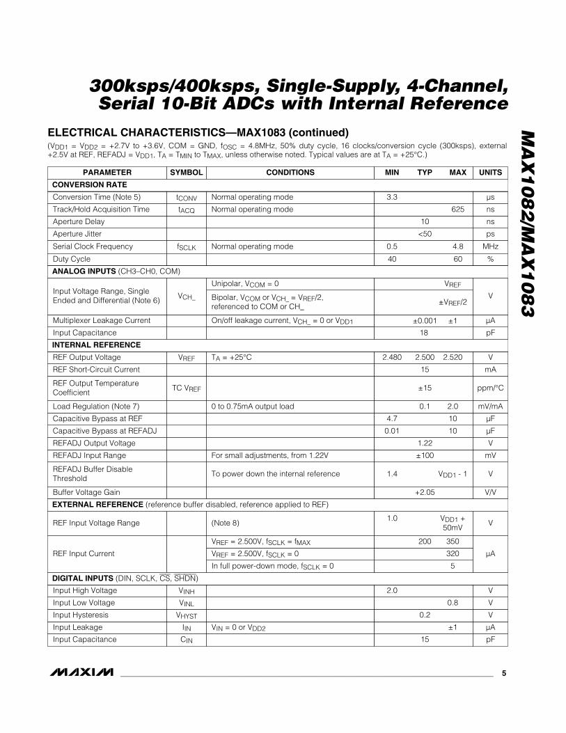
ELECTRICAL CHARACTERISTICS—MAX1083 (continued)(VDD1 = VDD2 = +2.7V to +3.6V, COM = GND, fOSC = 4.8MHz, 50% duty cycle, 16 clocks/conversion cycle (300ksps), external+2.5V at REF, REFADJ = VDD1, TA = TMIN to TMAX, unless otherwise noted. Typical values are at TA = +25°C.)
Normal operating mode
Normal operating mode
Normal operating mode
CONDITIONS
MHz0.5 4.8fSCLKSerial Clock Frequency
ps<50Aperture Jitter
ns10Aperture Delay
ns625tACQTrack/Hold Acquisition Time
µs3.3tCONVConversion Time (Note 5)
UNITSMIN TYP MAXSYMBOLPARAMETER
To power down the internal reference
For small adjustments, from 1.22V
0 to 0.75mA output load
On/off leakage current, VCH_ = 0 or VDD1
TA = +25°C
Bipolar, VCOM or VCH_ = VREF/2, referenced to COM or CH_
Unipolar, VCOM = 0
V/V2.05Buffer Voltage Gain
V1.4 VDD1 - 1REFADJ Buffer DisableThreshold
mV±100REFADJ Input Range
V1.22REFADJ Output Voltage
µF0.01 10Capacitive Bypass at REFADJ
µF4.7 10Capacitive Bypass at REF
mV/mA0.1 2.0Load Regulation (Note 7)
ppm/°C±15TC VREFREF Output TemperatureCoefficient
mA15REF Short-Circuit Current
V2.480 2.500 2.520VREFREF Output Voltage
pF18Input Capacitance
µA±0.001 ±1Multiplexer Leakage Current
±VREF/2
%40 60Duty Cycle
V
VREF
VCH_Input Voltage Range, SingleEnded and Differential (Note 6)
VIN = 0 or VDD2
In full power-down mode, fSCLK = 0
VREF = 2.500V, fSCLK = 0
VREF = 2.500V, fSCLK = fMAX
(Note 8)
pF15CINInput Capacitance
µA±1IINInput Leakage
V0.2VHYSTInput Hysteresis
V0.8VINLInput Low Voltage
V2.0VINHInput High Voltage
5
REF Input Current 320 µA
200 350
V1.0 VDD1 +
50mVREF Input Voltage Range
V/V+2.05Buffer Voltage Gain
CONVERSION RATE
ANALOG INPUTS (CH3–CH0, COM)
INTERNAL REFERENCE
EXTERNAL REFERENCE (reference buffer disabled, reference applied to REF)
DIGITAL INPUTS (DIN, SCLK, CS, SHDN)
MA
X1
08
2/M
AX
10
83
300ksps/400ksps, Single-Supply, 4-Channel,Serial 10-Bit ADCs with Internal Reference
6 _______________________________________________________________________________________
VDD1 =VDD2 =3.6V
ISOURCE = 0.5mA
VDD1 = VDD2 = 2.7V to 3.6V, midscale input
CONDITIONS
mA
2.5 3.5
IVDD1+ IVDD2
Supply Current
V2.7 3.6VDD1,VDD2
VVDD2 - 0.5VVOHOutput Voltage High
Positive Supply Voltage(Note 9)
1.3 2.0
Normal operating mode (Note 10)
Reduced-power mode (Note 11)
0.9 1.5Fast power-down mode (Note 11)
Full power-down mode (Note 11) µA2.0 1.0
mV±0.5 ±2.0PSRPower-Supply Rejection
UNITSMIN TYP MAXSYMBOLPARAMETER
ISINK = 5mA V0.4VOLOutput Voltage Low
CS = VDD2 µA±10ILThree-State Leakage Current
CS = VDD2 pF15COUTThree-State Output Capacitance
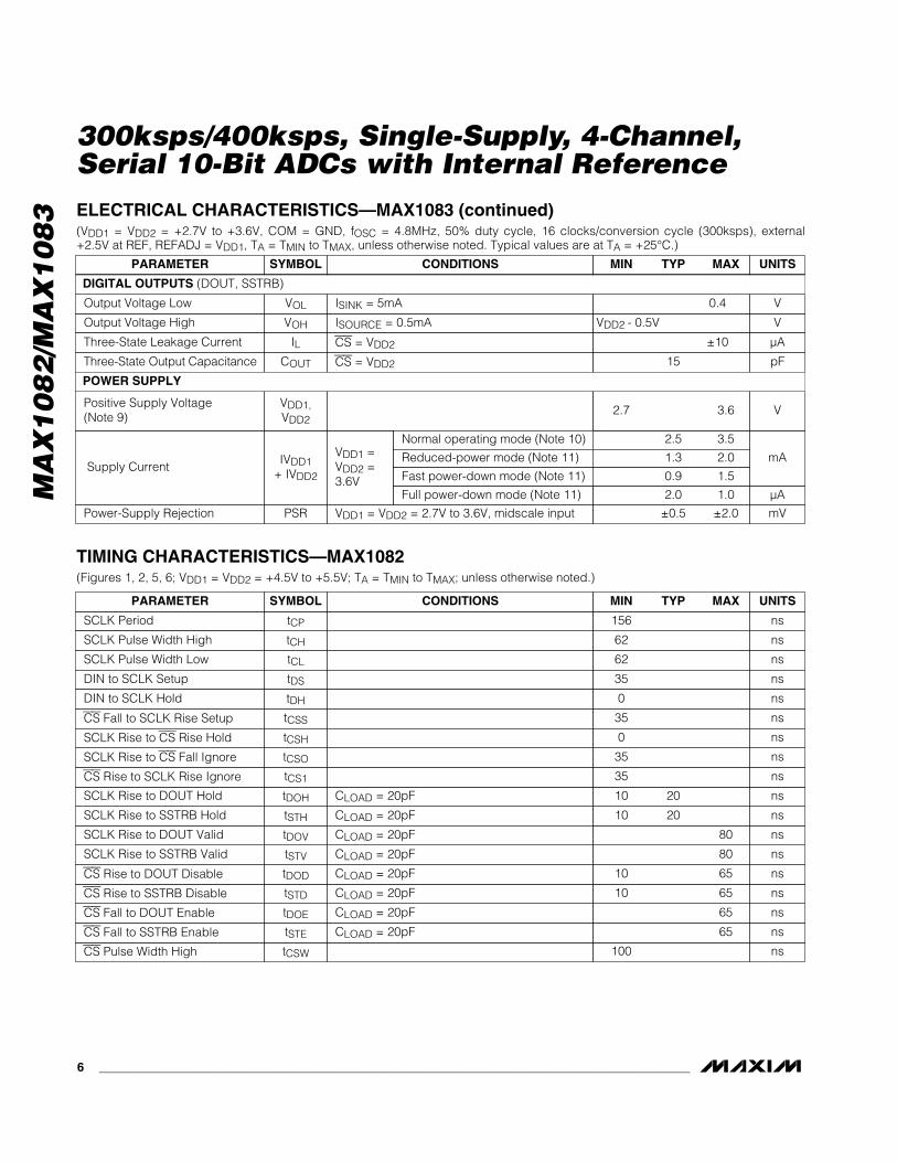
ELECTRICAL CHARACTERISTICS—MAX1083 (continued)(VDD1 = VDD2 = +2.7V to +3.6V, COM = GND, fOSC = 4.8MHz, 50% duty cycle, 16 clocks/conversion cycle (300ksps), external+2.5V at REF, REFADJ = VDD1, TA = TMIN to TMAX, unless otherwise noted. Typical values are at TA = +25°C.)
TIMING CHARACTERISTICS—MAX1082(Figures 1, 2, 5, 6; VDD1 = VDD2 = +4.5V to +5.5V; TA = TMIN to TMAX; unless otherwise noted.)
CLOAD = 20pF
CLOAD = 20pF
CLOAD = 20pF
CLOAD = 20pF
CLOAD = 20pF
CLOAD = 20pF
CLOAD = 20pF
CLOAD = 20pF
CONDITIONS
ns100tCSWCS Pulse Width High
ns65tSTECS Fall to SSTRB Enable
ns65tDOECS Fall to DOUT Enable
ns10 65tSTDCS Rise to SSTRB Disable
ns10 65tDODCS Rise to DOUT Disable
ns80tSTVSCLK Rise to SSTRB Valid
ns80tDOVSCLK Rise to DOUT Valid
ns62tCLSCLK Pulse Width Low
ns62tCH
ns156tCPSCLK Period
SCLK Pulse Width High
ns10 20tSTHSCLK Rise to SSTRB Hold
ns10 20tDOHSCLK Rise to DOUT Hold
ns35tCS1CS Rise to SCLK Rise Ignore
ns35tCSOSCLK Rise to CS Fall Ignore
ns35tDSDIN to SCLK Setup
ns0tDHDIN to SCLK Hold
ns35tCSSCS Fall to SCLK Rise Setup
ns0tCSHSCLK Rise to CS Rise Hold
UNITSMIN TYP MAXSYMBOLPARAMETER
DIGITAL OUTPUTS (DOUT, SSTRB)
POWER SUPPLY
MA
X1
08
2/M
AX
10
83
300ksps/400ksps, Single-Supply, 4-Channel,Serial 10-Bit ADCs with Internal Reference
_______________________________________________________________________________________ 7
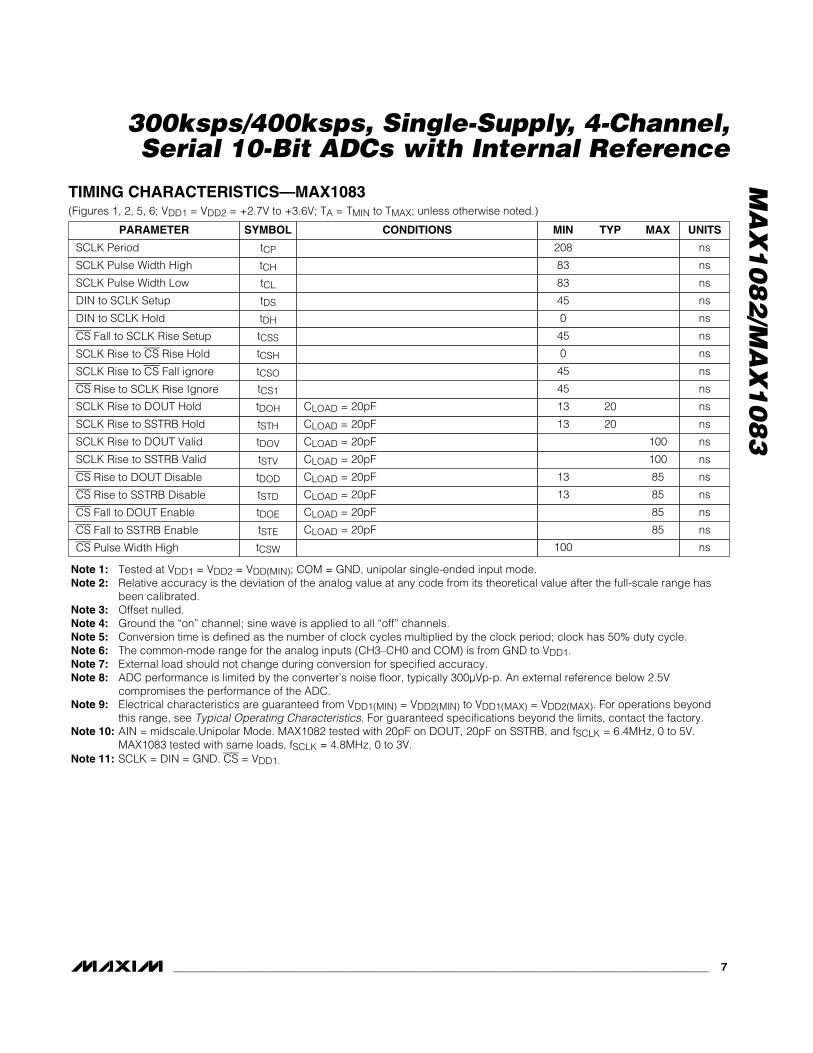
TIMING CHARACTERISTICS—MAX1083(Figures 1, 2, 5, 6; VDD1 = VDD2 = +2.7V to +3.6V; TA = TMIN to TMAX; unless otherwise noted.)
CLOAD = 20pF
CLOAD = 20pF
CLOAD = 20pF
CLOAD = 20pF
CLOAD = 20pF
CLOAD = 20pF
CLOAD = 20pF
CLOAD = 20pF
CONDITIONS
ns100tCSWCS Pulse Width High
ns85tSTECS Fall to SSTRB Enable
ns85tDOECS Fall to DOUT Enable
ns13 85tSTDCS Rise to SSTRB Disable
ns13 85tDODCS Rise to DOUT Disable
ns100tSTVSCLK Rise to SSTRB Valid
ns100tDOVSCLK Rise to DOUT Valid
ns83tCLSCLK Pulse Width Low
ns83 tCH
ns208tCPSCLK Period
SCLK Pulse Width High
ns13 20tSTHSCLK Rise to SSTRB Hold
ns13 20tDOHSCLK Rise to DOUT Hold
ns45tCS1CS Rise to SCLK Rise Ignore
ns45tCSOSCLK Rise to CS Fall ignore
ns45tDSDIN to SCLK Setup
ns0tDHDIN to SCLK Hold
ns45tCSSCS Fall to SCLK Rise Setup
ns0tCSHSCLK Rise to CS Rise Hold
UNITSMIN TYP MAXSYMBOLPARAMETER
Note 1: Tested at VDD1 = VDD2 = VDD(MIN); COM = GND, unipolar single-ended input mode.Note 2: Relative accuracy is the deviation of the analog value at any code from its theoretical value after the full-scale range has
been calibrated.Note 3: Offset nulled.Note 4: Ground the “on” channel; sine wave is applied to all “off” channels.Note 5: Conversion time is defined as the number of clock cycles multiplied by the clock period; clock has 50% duty cycle.Note 6: The common-mode range for the analog inputs (CH3–CH0 and COM) is from GND to VDD1.Note 7: External load should not change during conversion for specified accuracy.Note 8: ADC performance is limited by the converter’s noise floor, typically 300µVp-p. An external reference below 2.5V
compromises the performance of the ADC.Note 9: Electrical characteristics are guaranteed from VDD1(MIN) = VDD2(MIN) to VDD1(MAX) = VDD2(MAX). For operations beyond
this range, see Typical Operating Characteristics. For guaranteed specifications beyond the limits, contact the factory.Note 10: AIN = midscale.Unipolar Mode. MAX1082 tested with 20pF on DOUT, 20pF on SSTRB, and fSCLK = 6.4MHz, 0 to 5V.
MAX1083 tested with same loads, fSCLK = 4.8MHz, 0 to 3V.Note 11: SCLK = DIN = GND. CS = VDD1.
MA
X1
08
2/M
AX
10
83
300ksps/400ksps, Single-Supply, 4-Channel,Serial 10-Bit ADCs with Internal Reference
8 _______________________________________________________________________________________
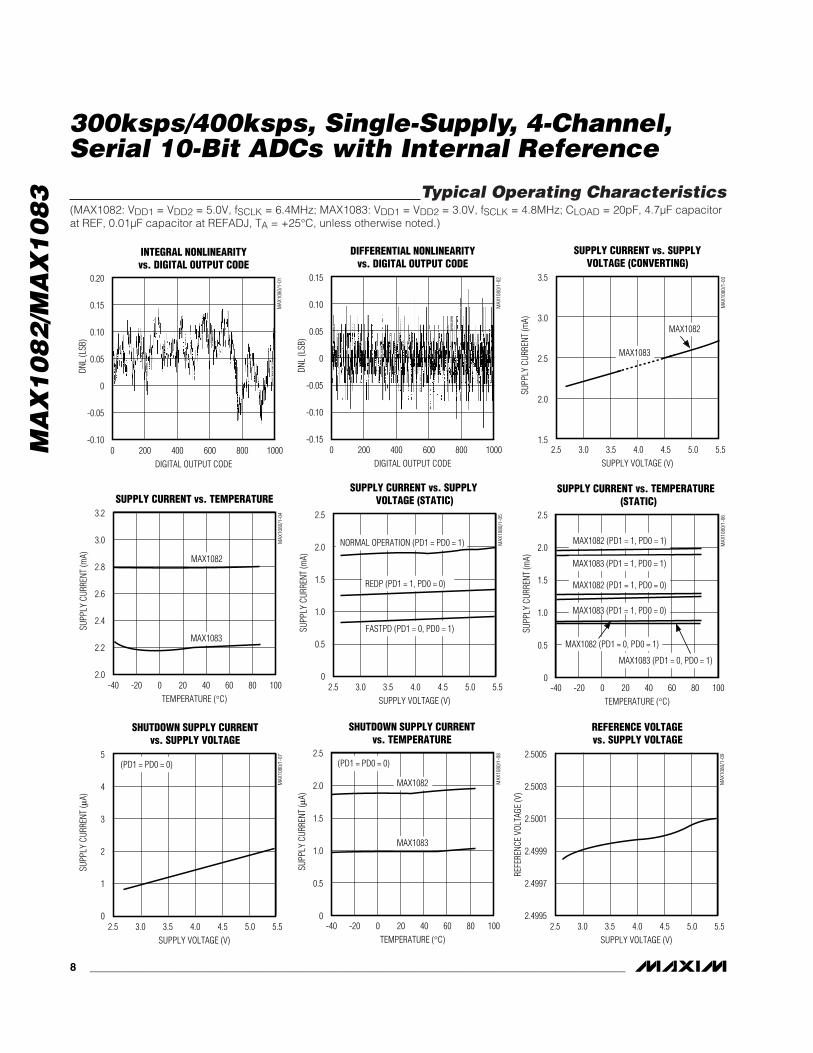
Typical Operating Characteristics(MAX1082: VDD1 = VDD2 = 5.0V, fSCLK = 6.4MHz; MAX1083: VDD1 = VDD2 = 3.0V, fSCLK = 4.8MHz; CLOAD = 20pF, 4.7µF capacitorat REF, 0.01µF capacitor at REFADJ, TA = +25°C, unless otherwise noted.)
-0.10
0
-0.05
0.10
0.05
0.15
0.20
0 400200 600 800 1000
INTEGRAL NONLINEARITYvs. DIGITAL OUTPUT CODE
MAX
1080
/1-0
1
DIGITAL OUTPUT CODE
DNL
(LSB
)
-0.15
-0.05
-0.10
0.05
0
0.10
0.15
0 400200 600 800 1000
DIFFERENTIAL NONLINEARITYvs. DIGITAL OUTPUT CODE
MAX
1080
/1-0
2
DIGITAL OUTPUT CODE
DNL
(LSB
)
3.5
3.0
2.5
2.0
1.52.5 4.03.0 3.5 4.5 5.0 5.5
SUPPLY CURRENT vs. SUPPLY VOLTAGE (CONVERTING)
MAX
1080
/1-0
3
SUPPLY VOLTAGE (V)
SUPP
LY C
URRE
NT (m
A)
MAX1083
MAX1082
2.0
2.4
2.2
2.8
2.6
3.0
3.2
-40 20 40-20 0 60 80 100
SUPPLY CURRENT vs. TEMPERATURE
MAX
1080
/1-0
4
TEMPERATURE (°C)
SUPP
LY C
URRE
NT (m
A)
MAX1083
MAX1082
NORMAL OPERATION (PD1 = PD0 = 1)
REDP (PD1 = 1, PD0 = 0)
FASTPD (PD1 = 0, PD0 = 1)
0
0.5
1.5
1.0
2.0
2.5
2.5 3.53.0 4.0 4.5 5.0 5.5
SUPPLY CURRENT vs. SUPPLY VOLTAGE (STATIC)
MAX
1080
/1-0
5
SUPPLY VOLTAGE (V)
SUPP
LY C
URRE
NT (m
A)
0
0.5
1.5
1.0
2.0
2.5
-40 0-20 20 40 60 80 100
SUPPLY CURRENT vs. TEMPERATURE (STATIC)
MAX
1080
/1-0
6
TEMPERATURE (°C)
SUPP
LY C
URRE
NT (m
A)
MAX1082 (PD1 = 1, PD0 = 1)
MAX1082 (PD1 = 1, PD0 = 0)
MAX1082 (PD1 = 0, PD0 = 1)
MAX1083 (PD1 = 1, PD0 = 1)
MAX1083 (PD1 = 1, PD0 = 0)
MAX1083 (PD1 = 0, PD0 = 1)
0
1
3
2
4
5
2.5 3.53.0 4.0 4.5 5.0 5.5
SHUTDOWN SUPPLY CURRENT vs. SUPPLY VOLTAGE
MAX
1080
/1-0
7
SUPPLY VOLTAGE (V)
SUPP
LY C
URRE
NT (µ
A)
(PD1 = PD0 = 0)
0
0.5
1.5
1.0
2.0
2.5
-40 0-20 20 40 60 80 100
SHUTDOWN SUPPLY CURRENT vs. TEMPERATURE
MAX
1080
/1-0
8
TEMPERATURE (°C)
SUPP
LY C
URRE
NT (µ
A)
MAX1083
MAX1082
(PD1 = PD0 = 0)
2.4995
2.4997
2.5001
2.4999
2.5003
2.5005
2.5 3.53.0 4.0 4.5 5.0 5.5
REFERENCE VOLTAGE vs. SUPPLY VOLTAGE
MAX
1080
/1-0
9
SUPPLY VOLTAGE (V)
REFE
RENC
E VO
LTAG
E (V
)

MA
X1
08
2/M
AX
10
83
300ksps/400ksps, Single-Supply, 4-Channel,Serial 10-Bit ADCs with Internal Reference
_______________________________________________________________________________________ 9
2.4988
2.4992
2.4990
2.4996
2.4994
2.5000
2.4998
2.5002
-40 0 20-20 40 60 80 100
REFERENCE VOLTAGEvs. TEMPERATURE
MAX
1080
/1-1
0
TEMPERATURE (°C)
REFE
RENC
E VO
LTAG
E (V
)
MAX1083
MAX1082
-0.50
-0.25
0
0.25
0.50
2.5 3.53.0 4.0 4.5 5.0 5.5
OFFSET ERROR vs. SUPPLY VOLTAGE
MAX
1082
/3-1
1
SUPPLY VOLTAGE (V)
OFFS
ET E
RROR
(LSB
)
-0.50
-0.25
0
-40 10-15 35 60 85
OFFSET ERROR vs. TEMPERATURE
MAX
1080
/1-1
2
TEMPERATURE (°C)
OFFS
ET E
RROR
(LSB
)
-0.25
-0.10
-0.15
-0.20
-0.05
0
0.05
0.10
0.15
0.20
0.25
2.5 3.53.0 4.0 4.5 5.0 5.5
GAIN ERROR vs. SUPPLY VOLTAGE
MAX
1082
/3-1
3
SUPPLY VOLTAGE (V)
GAIN
ERR
OR (L
SB)
-.50
-.25
0
GAIN ERROR vs. TEMPERATURE
MAX
1080
/1-1
4
TEMPERATURE (°C)
GAIN
ERR
OR (L
SB)
-40 10-15 35 60 85
Typical Operating Characteristics (continued)(MAX1082: VDD1 = VDD2 = 5.0V, fSCLK = 6.4MHz; MAX1083: VDD1 = VDD2 = 3.0V, fSCLK = 4.8MHz; CLOAD = 20pF, 4.7µF capacitorat REF, 0.01µF capacitor at REFADJ, TA = +25°C, unless otherwise noted.)
MA
X1
08
2/M
AX
10
83
300ksps/400ksps, Single-Supply, 4-Channel,Serial 10-Bit ADCs with Internal Reference
10 ______________________________________________________________________________________
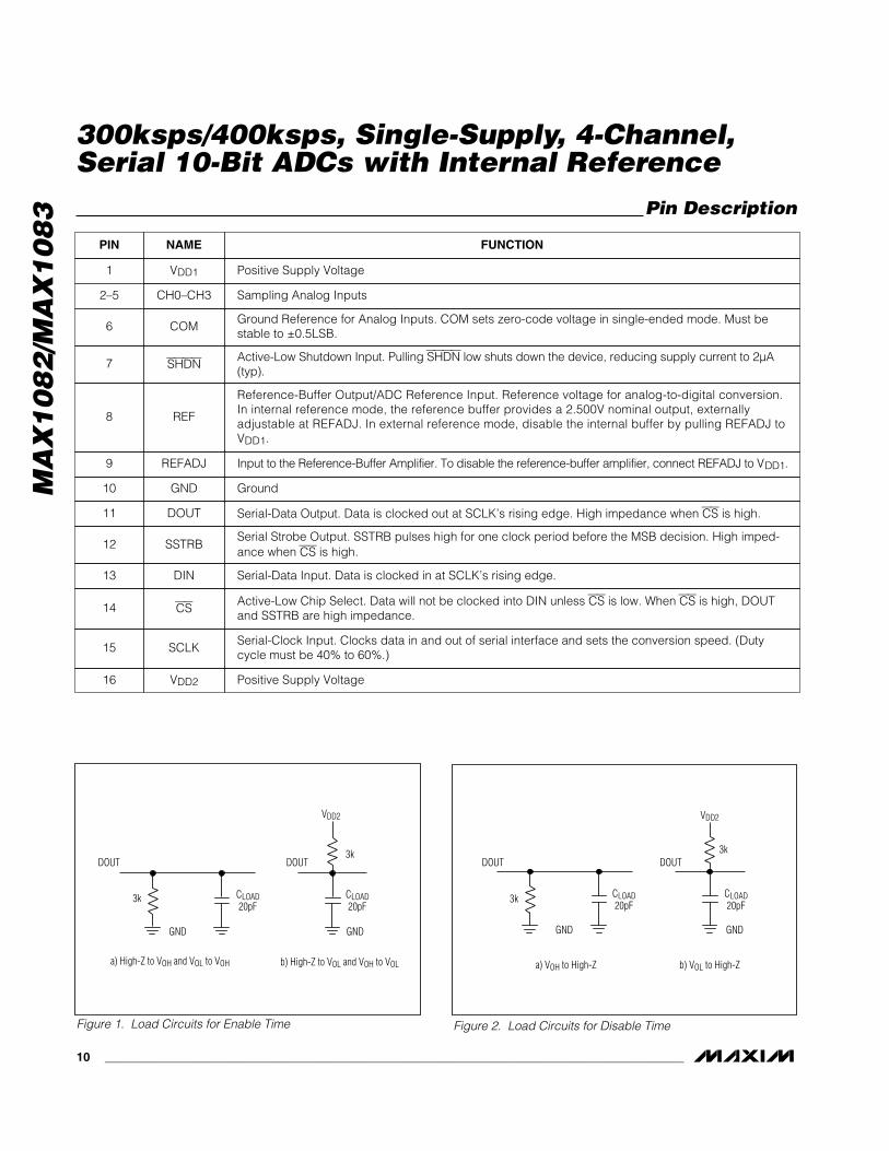
Pin Description
Positive Supply VoltageVDD216
Input to the Reference-Buffer Amplifier. To disable the reference-buffer amplifier, connect REFADJ to VDD1.REFADJ9
Serial Strobe Output. SSTRB pulses high for one clock period before the MSB decision. High imped-ance when CS is high.
SSTRB12
Serial-Data Input. Data is clocked in at SCLK’s rising edge.DIN13
Active-Low Chip Select. Data will not be clocked into DIN unless CS is low. When CS is high, DOUTand SSTRB are high impedance.
CS14
Serial-Clock Input. Clocks data in and out of serial interface and sets the conversion speed. (Dutycycle must be 40% to 60%.)
SCLK15
Reference-Buffer Output/ADC Reference Input. Reference voltage for analog-to-digital conversion.In internal reference mode, the reference buffer provides a 2.500V nominal output, externallyadjustable at REFADJ. In external reference mode, disable the internal buffer by pulling REFADJ toVDD1.
REF8
GroundGND10
Serial-Data Output. Data is clocked out at SCLK’s rising edge. High impedance when CS is high.DOUT11
Active-Low Shutdown Input. Pulling SHDN low shuts down the device, reducing supply current to 2µA(typ).
SHDN7
Ground Reference for Analog Inputs. COM sets zero-code voltage in single-ended mode. Must be stable to ±0.5LSB.
COM6
PIN
Positive Supply VoltageVDD11
FUNCTIONNAME
VDD2
3k
GND
DOUT
CLOAD20pF
CLOAD20pF
GND
3k
DOUT
a) High-Z to VOH and VOL to VOH b) High-Z to VOL and VOH to VOL
VDD2
3k
GND
DOUT
CLOAD20pF
CLOAD20pF
GND
3k
DOUT
a) VOH to High-Z b) VOL to High-Z
Figure 1. Load Circuits for Enable Time Figure 2. Load Circuits for Disable Time
Sampling Analog InputsCH0–CH32–5
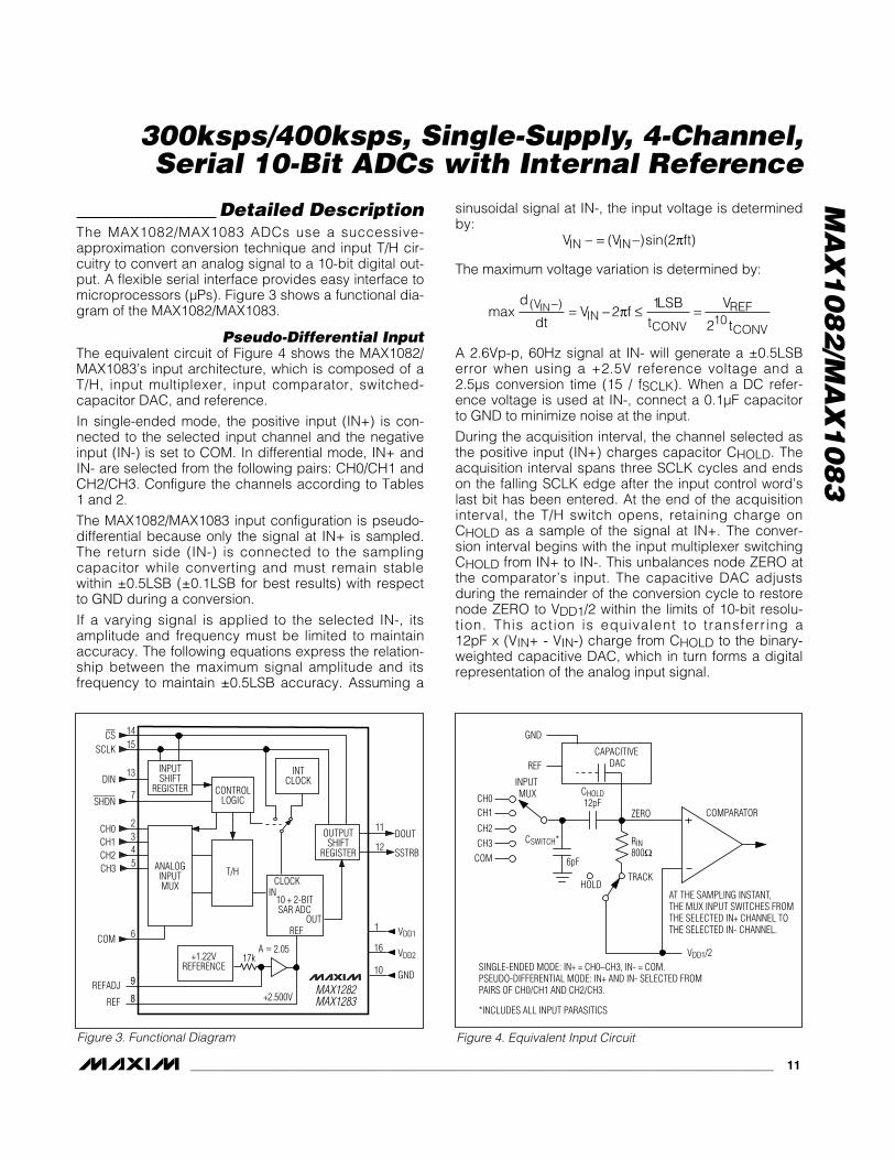
Detailed DescriptionThe MAX1082/MAX1083 ADCs use a successive-approximation conversion technique and input T/H cir-cuitry to convert an analog signal to a 10-bit digital out-put. A flexible serial interface provides easy interface tomicroprocessors (µPs). Figure 3 shows a functional dia-gram of the MAX1082/MAX1083.
Pseudo-Differential InputThe equivalent circuit of Figure 4 shows the MAX1082/MAX1083’s input architecture, which is composed of aT/H, input multiplexer, input comparator, switched-capacitor DAC, and reference.
In single-ended mode, the positive input (IN+) is con-nected to the selected input channel and the negativeinput (IN-) is set to COM. In differential mode, IN+ andIN- are selected from the following pairs: CH0/CH1 andCH2/CH3. Configure the channels according to Tables1 and 2.
The MAX1082/MAX1083 input configuration is pseudo-differential because only the signal at IN+ is sampled.The return side (IN-) is connected to the samplingcapacitor while converting and must remain stablewithin ±0.5LSB (±0.1LSB for best results) with respectto GND during a conversion.
If a varying signal is applied to the selected IN-, itsamplitude and frequency must be limited to maintainaccuracy. The following equations express the relation-ship between the maximum signal amplitude and itsfrequency to maintain ±0.5LSB accuracy. Assuming a
sinusoidal signal at IN-, the input voltage is determinedby:
The maximum voltage variation is determined by:
A 2.6Vp-p, 60Hz signal at IN- will generate a ±0.5LSBerror when using a +2.5V reference voltage and a2.5µs conversion time (15 / fSCLK). When a DC refer-ence voltage is used at IN-, connect a 0.1µF capacitorto GND to minimize noise at the input.
During the acquisition interval, the channel selected asthe positive input (IN+) charges capacitor CHOLD. Theacquisition interval spans three SCLK cycles and endson the falling SCLK edge after the input control word’slast bit has been entered. At the end of the acquisitioninterval, the T/H switch opens, retaining charge onCHOLD as a sample of the signal at IN+. The conver-sion interval begins with the input multiplexer switchingCHOLD from IN+ to IN-. This unbalances node ZERO atthe comparator’s input. The capacitive DAC adjustsduring the remainder of the conversion cycle to restorenode ZERO to VDD1/2 within the limits of 10-bit resolu-tion. This action is equivalent to transferring a 12pF x (VIN+ - VIN-) charge from CHOLD to the binary-weighted capacitive DAC, which in turn forms a digitalrepresentation of the analog input signal.
max( )d
dtV f
LSBt
V
t
VIN
CONV
REF
CONV
IN− = − ≤ =21
210π
V V ftIN IN− = −( )sin( )2π
MA
X1
08
2/M
AX
10
83
300ksps/400ksps, Single-Supply, 4-Channel,Serial 10-Bit ADCs with Internal Reference
______________________________________________________________________________________ 11
INPUTSHIFT
REGISTER CONTROLLOGIC
INTCLOCK
OUTPUTSHIFT
REGISTER
+1.22VREFERENCE
T/HANALOGINPUTMUX
10 + 2-BITSAR ADC
IN
DOUT
SSTRB
VDD1
VDD2
GND
SCLK
DIN
COM
REFADJ
REF
OUTREF
CLOCK
+2.500V
17k
7
8
9
6
11
12
13
1415
CH1 3
CH2 4
CH3 5
CH0 2
MAX1282MAX1283
CS
SHDN
1
16
10
2.05A ≈
Figure 3. Functional Diagram
CHOLD12pF
RIN800Ω
HOLD
INPUT MUX
CSWITCH*
*INCLUDES ALL INPUT PARASITICS
SINGLE-ENDED MODE: IN+ = CH0–CH3, IN- = COM.PSEUDO-DIFFERENTIAL MODE: IN+ AND IN- SELECTED FROM PAIRS OF CH0/CH1 AND CH2/CH3.
AT THE SAMPLING INSTANT, THE MUX INPUT SWITCHES FROMTHE SELECTED IN+ CHANNEL TO THE SELECTED IN- CHANNEL.
CH0
REF
GND
CH1
CH2CH3
COM
ZERO
VDD1/2
COMPARATOR
CAPACITIVE DAC
6pFTRACK
Figure 4. Equivalent Input Circuit

MA
X1
08
2/M
AX
10
83
300ksps/400ksps, Single-Supply, 4-Channel,Serial 10-Bit ADCs with Internal Reference
12 ______________________________________________________________________________________
Track/HoldThe T/H enters its tracking mode on the falling clockedge after the fifth bit of the 8-bit control word has beenshifted in. It enters its hold mode on the falling clockedge after the eighth bit of the control word has beenshifted in. If the converter is set up for single-endedinputs, IN- is connected to COM and the convertersamples the “+” input. If the converter is set up for dif-ferential inputs, the difference of [(IN+) - (IN-)] is con-verted. At the end of the conversion, the positive inputconnects back to IN+ and CHOLD charges to the inputsignal.
The time required for the T/H to acquire an input signalis a function of how quickly its input capacitance ischarged. If the input signal’s source impedance is high,the acquisition time lengthens, and more time must beallowed between conversions. The acquisition time, tACQ, is the maximum time the device takes to acquirethe signal and the minimum time needed for the signalto be acquired. It is calculated by the following equa-tion:
tACQ = 7 x (RS + RIN) x 18pF
where RIN = 800Ω, RS = the source impedance of theinput signal, and tACQ is never less than 400ns(MAX1082) or 625ns (MAX1083). Note that sourceimpedances below 4kΩ do not significantly affect theADC’s AC performance.
Input BandwidthThe ADC’s input tracking circuitry has a 6MHz(MAX1082) or 3MHz (MAX1083) small-signal band-width, so it is possible to digitize high-speed transientevents and measure periodic signals with bandwidthsexceeding the ADC’s sampling rate by using under-sampling techniques. To avoid high-frequency signalsbeing aliased into the frequency band of interest, anti-alias filtering is recommended.
Analog Input ProtectionInternal protection diodes, which clamp the analog inputto VDD1 and GND, allow the channel input pins to swingfrom GND - 0.3V to VDD1 + 0.3V without damage.However, for accurate conversions near full scale, theinputs must not exceed VDD1 by more than 50mV or belower than GND by 50mV.
If the analog input exceeds 50mV beyond the sup-plies, do not allow the input current to exceed 2mA.
How to Start a ConversionStart a conversion by clocking a control byte into DIN.With CS low, each rising edge on SCLK clocks a bit from
DIN into the MAX1082/MAX1083’s internal shift register.After CS falls, the first arriving logic “1” bit defines thecontrol byte’s MSB. Until this first “start” bit arrives, anynumber of logic “0” bits can be clocked into DIN with noeffect. Table 3 shows the control-byte format.
The MAX1082/MAX1083 are compatible with SPI/QSPI and MICROWIRE devices. For SPI, select the cor-rect clock polarity and sampling edge in the SPI controlregisters: set CPOL = 0 and CPHA = 0. MICROWIRE,SPI, and QSPI all transmit a byte and receive a byte atthe same time. Using the Typical Operating Circuit, thesimplest software interface requires only three 8-bittransfers to perform a conversion (one 8-bit transfer toconfigure the ADC, and two more 8-bit transfers to clockout the conversion result). See Figure 16 for MAX1082/MAX1083 QSPI connections.
Simple Software InterfaceMake sure the CPU’s serial interface runs in mastermode so the CPU generates the serial clock. Choose aclock frequency from 500kHz to 6.4MHz (MAX1082) or4.8MHz (MAX1083).
1) Set up the control byte and call it TB1. TB1 shouldbe of the format: 1XXXXXXX binary, where the Xsdenote the particular channel, selected conversionmode, and power mode.
2) Use a general-purpose I/O line on the CPU to pull CS low.
3) Transmit TB1 and, simultaneously, receive a byte and call it RB1. Ignore RB1.
4) Transmit a byte of all zeros ($00 hex) and, simulta-neously, receive byte RB2.
5) Transmit a byte of all zeros ($00 hex) and, simulta-neously, receive byte RB3.
6) Pull CS high.
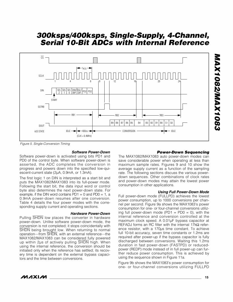
Figure 5 shows the timing for this sequence. Bytes RB2and RB3 contain the result of the conversion, paddedwith three leading zeros, two sub-LSB bits, and onetrailing zero. The total conversion time is a function ofthe serial-clock frequency and the amount of idle timebetween 8-bit transfers. To avoid excessive T/H droop,make sure the total conversion time does not exceed120µs.
Digital OutputIn unipolar input mode, the output is straight binary(Figure 13). For bipolar input mode, the output is two’scomplement (Figure 14). Data is clocked out on the ris-ing edge of SCLK in MSB-first format.
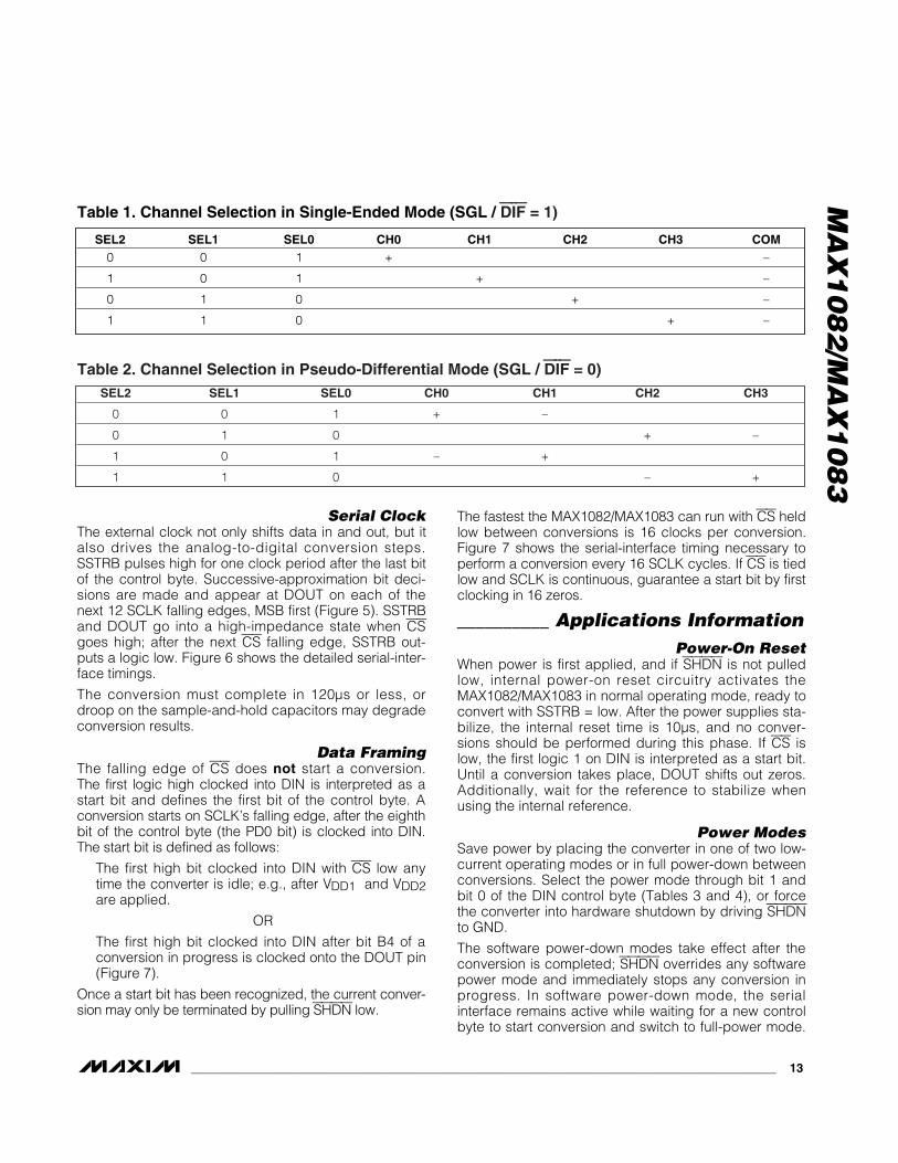
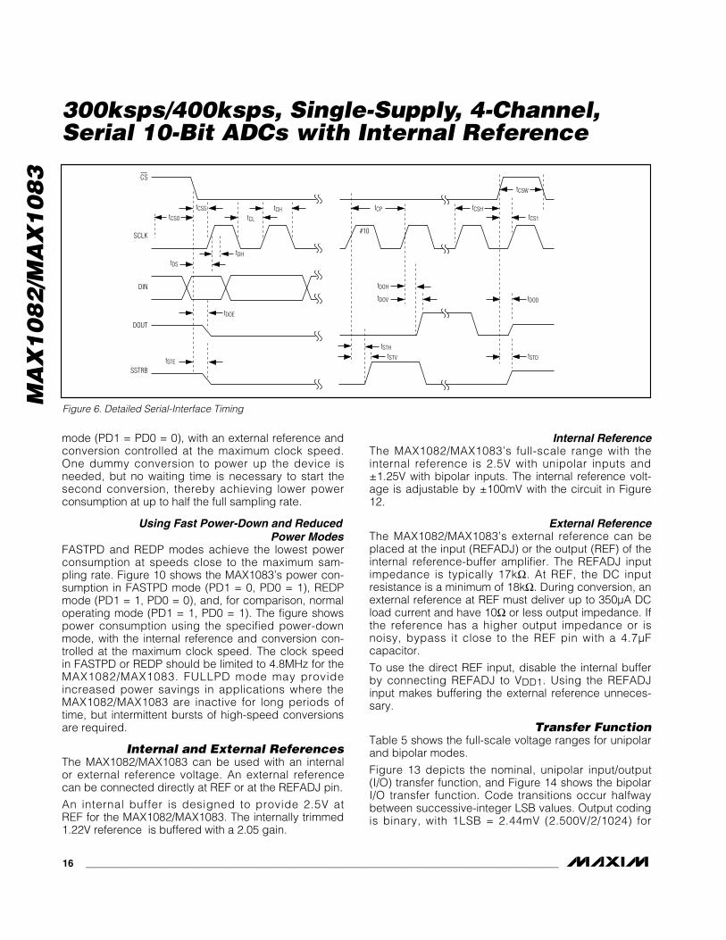
Serial ClockThe external clock not only shifts data in and out, but italso drives the analog-to-digital conversion steps.SSTRB pulses high for one clock period after the last bitof the control byte. Successive-approximation bit deci-sions are made and appear at DOUT on each of thenext 12 SCLK falling edges, MSB first (Figure 5). SSTRBand DOUT go into a high-impedance state when CSgoes high; after the next CS falling edge, SSTRB out-puts a logic low. Figure 6 shows the detailed serial-inter-face timings.
The conversion must complete in 120µs or less, ordroop on the sample-and-hold capacitors may degradeconversion results.
Data FramingThe falling edge of CS does not start a conversion. The first logic high clocked into DIN is interpreted as astart bit and defines the first bit of the control byte. Aconversion starts on SCLK’s falling edge, after the eighthbit of the control byte (the PD0 bit) is clocked into DIN.The start bit is defined as follows:
The first high bit clocked into DIN with CS low anytime the converter is idle; e.g., after VDD1 and VDD2are applied.
OR
The first high bit clocked into DIN after bit B4 of aconversion in progress is clocked onto the DOUT pin(Figure 7).
Once a start bit has been recognized, the current conver-sion may only be terminated by pulling SHDN low.
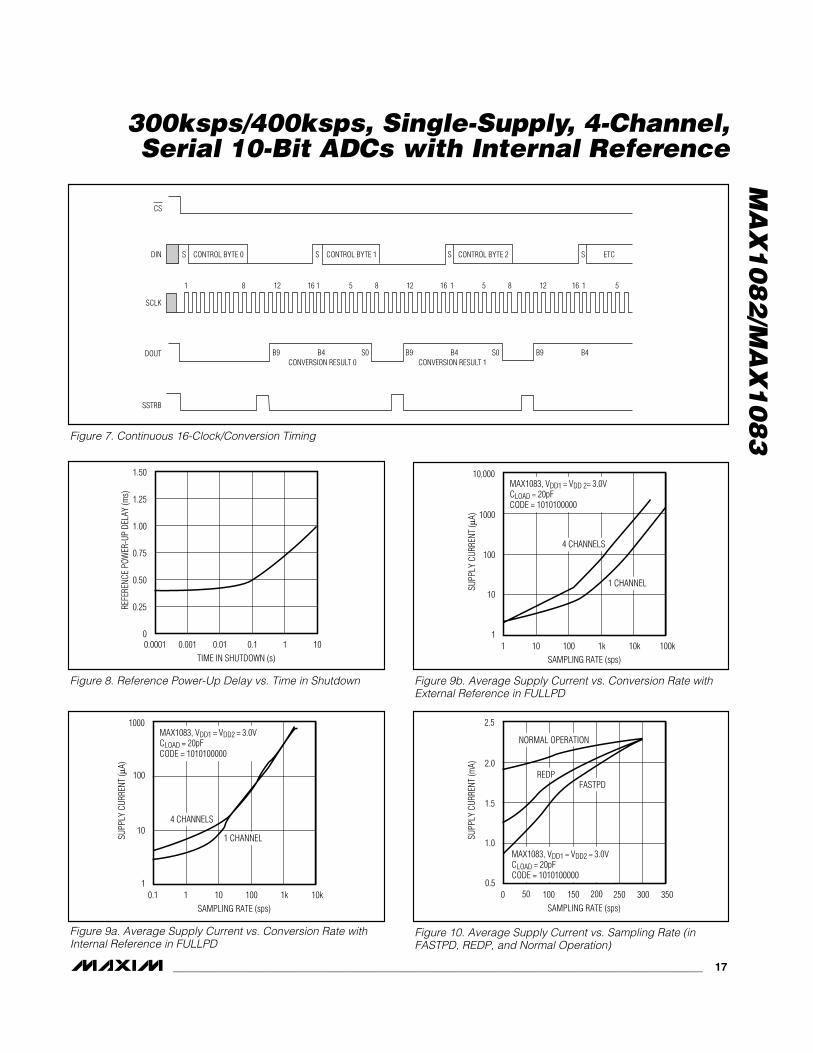
The fastest the MAX1082/MAX1083 can run with CS heldlow between conversions is 16 clocks per conversion.Figure 7 shows the serial-interface timing necessary toperform a conversion every 16 SCLK cycles. If CS is tiedlow and SCLK is continuous, guarantee a start bit by firstclocking in 16 zeros.
__________ Applications InformationPower-On Reset
When power is first applied, and if SHDN is not pulledlow, internal power-on reset circuitry activates theMAX1082/MAX1083 in normal operating mode, ready toconvert with SSTRB = low. After the power supplies sta-bilize, the internal reset time is 10µs, and no conver-sions should be performed during this phase. If CS islow, the first logic 1 on DIN is interpreted as a start bit.Until a conversion takes place, DOUT shifts out zeros.Additionally, wait for the reference to stabilize whenusing the internal reference.
Power ModesSave power by placing the converter in one of two low-current operating modes or in full power-down betweenconversions. Select the power mode through bit 1 andbit 0 of the DIN control byte (Tables 3 and 4), or forcethe converter into hardware shutdown by driving SHDNto GND.
The software power-down modes take effect after theconversion is completed; SHDN overrides any softwarepower mode and immediately stops any conversion inprogress. In software power-down mode, the serialinterface remains active while waiting for a new controlbyte to start conversion and switch to full-power mode.
MA
X1
08
2/M
AX
10
83
______________________________________________________________________________________ 13
SEL2 SEL1 SEL0 CH0 CH1 CH2 CH3 COM0 0 1 + –
1 0 1 + –
0 1 0 + –
1 1 0 + –
Table 1. Channel Selection in Single-Ended Mode (SGL / DIF = 1)
SEL2 SEL1 SEL0 CH0 CH1 CH2 CH3
0 0 1 + –
0 1 0 + –
1 0 1 – +
1 1 0 – +
Table 2. Channel Selection in Pseudo-Differential Mode (SGL / DIF = 0)
MA
X1
08
2/M
AX
10
83
300ksps/400ksps, Single-Supply, 4-Channel,Serial 10-Bit ADCs with Internal Reference
14 ______________________________________________________________________________________
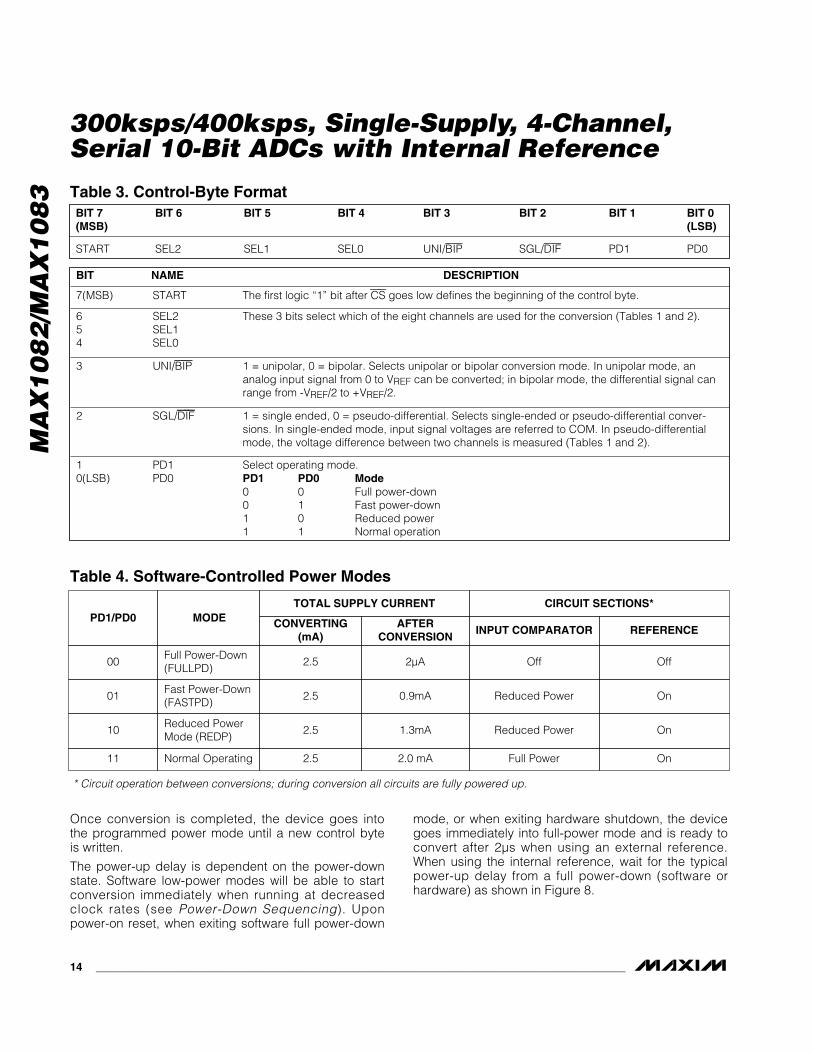
BIT NAME DESCRIPTION
7(MSB) START The first logic “1” bit after CS goes low defines the beginning of the control byte.
6 SEL2 These 3 bits select which of the eight channels are used for the conversion (Tables 1 and 2).5 SEL14 SEL0
3 UNI/BIP 1 = unipolar, 0 = bipolar. Selects unipolar or bipolar conversion mode. In unipolar mode, an analog input signal from 0 to VREF can be converted; in bipolar mode, the differential signal can range from -VREF/2 to +VREF/2.
2 SGL/DIF 1 = single ended, 0 = pseudo-differential. Selects single-ended or pseudo-differential conver-sions. In single-ended mode, input signal voltages are referred to COM. In pseudo-differential mode, the voltage difference between two channels is measured (Tables 1 and 2).
1 PD1 Select operating mode.0(LSB) PD0 PD1 PD0 Mode
0 0 Full power-down0 1 Fast power-down 1 0 Reduced power1 1 Normal operation
Table 3. Control-Byte FormatBIT 7 BIT 6 BIT 5 BIT 4 BIT 3 BIT 2 BIT 1 BIT 0(MSB) (LSB)
START SEL2 SEL1 SEL0 UNI/BIP SGL/DIF PD1 PD0
Once conversion is completed, the device goes intothe programmed power mode until a new control byteis written.
The power-up delay is dependent on the power-downstate. Software low-power modes will be able to startconversion immediately when running at decreasedclock rates (see Power-Down Sequencing). Uponpower-on reset, when exiting software full power-down
mode, or when exiting hardware shutdown, the devicegoes immediately into full-power mode and is ready toconvert after 2µs when using an external reference.When using the internal reference, wait for the typicalpower-up delay from a full power-down (software orhardware) as shown in Figure 8.
PD1/PD0 MODETOTAL SUPPLY CURRENT CIRCUIT SECTIONS*
CONVERTING(mA)
AFTERCONVERSION
INPUT COMPARATOR REFERENCE
00Full Power-Down(FULLPD)
2.5 2µA Off Off
01Fast Power-Down(FASTPD)
2.5 0.9mA Reduced Power On
10Reduced PowerMode (REDP)
2.5 1.3mA Reduced Power On
11 Normal Operating 2.5 2.0 mA Full Power On
Table 4. Software-Controlled Power Modes
* Circuit operation between conversions; during conversion all circuits are fully powered up.
MA
X1
08
2/M
AX
10
83
300ksps/400ksps, Single-Supply, 4-Channel,Serial 10-Bit ADCs with Internal Reference
______________________________________________________________________________________ 15
Software Power-DownSoftware power-down is activated using bits PD1 andPD0 of the control byte. When software power-down isasserted, the ADC completes the conversion inprogress and powers down into the specified low-qui-escent-current state (2µA, 0.9mA, or 1.3mA).
The first logic 1 on DIN is interpreted as a start bit andputs the MAX1082/MAX1083 into its full-power mode.Following the start bit, the data input word or controlbyte also determines the next power-down state. Forexample, if the DIN word contains PD1 = 0 and PD0 = 1, a0.9mA power-down resumes after one conversion.Table 4 details the four power modes with the corre-sponding supply current and operating sections.
Hardware Power-DownPulling SHDN low places the converter in hardwarepower-down. Unlike software power-down mode, theconversion is not completed; it stops coincidentally withSHDN being brought low. When returning to normaloperation—from SHDN, with an external reference—theMAX1082/MAX1083 can be considered fully poweredup within 2µs of actively pulling SHDN high. Whenusing the internal reference, the conversion should beinitiated only when the reference has settled; its recov-ery time is dependent on the external bypass capaci-tors and the time between conversions.
Power-Down SequencingThe MAX1082/MAX1083 auto power-down modes cansave considerable power when operating at less thanmaximum sample rates. Figures 9 and 10 show theaverage supply current as a function of the samplingrate. The following sections discuss the various power-down sequences. Other combinations of clock ratesand power-down modes may attain the lowest powerconsumption in other applications.
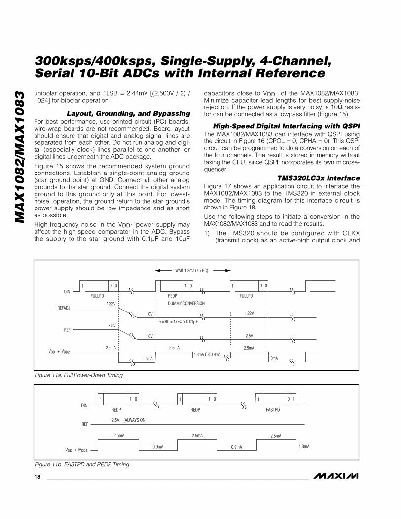
Using Full Power-Down ModeFull power-down mode (FULLPD) achieves the lowestpower consumption, up to 1000 conversions per chan-nel per second. Figure 9a shows the MAX1083’s powerconsumption for one- or four-channel conversions utiliz-ing full power-down mode (PD1 = PD0 = 0), with theinternal reference and conversion controlled at themaximum clock speed. A 0.01µF bypass capacitor atREFADJ forms an RC filter with the internal 17kΩ refer-ence resistor, with a 170µs time constant. To achievefull 10-bit accuracy, seven time constants or 1.2ms arerequired after power-up if the bypass capacitor is fullydischarged between conversions. Waiting this 1.2msduration in fast power-down (FASTPD) or reduced-power (REDP) mode instead of in full power-up can fur-ther reduce power consumption. This is achieved byusing the sequence shown in Figure 11a.
Figure 9b shows the MAX1083’s power consumption forone- or four-channel conversions utilizing FULLPD
400ns
(CLK = 6.4MHz)
IDLE
CS
SCLK
DIN
SSTRB
DOUT
A/D STATE
tACQ
IDLECONVERSION
RB3RB2RB1
SEL2
1
START
4 8 9 12 16 20 24
SEL1
SEL0
UNI/BIP
SGL/DIF PD2 PD2
B9 B8 B7 B6 B5 B4 B3 B2 B1 B0 S1 S0
Figure 5. Single-Conversion Timing
MA
X1
08
2/M
AX
10
83
mode (PD1 = PD0 = 0), with an external reference andconversion controlled at the maximum clock speed.One dummy conversion to power up the device isneeded, but no waiting time is necessary to start thesecond conversion, thereby achieving lower powerconsumption at up to half the full sampling rate.
Using Fast Power-Down and Reduced Power Modes
FASTPD and REDP modes achieve the lowest powerconsumption at speeds close to the maximum sam-pling rate. Figure 10 shows the MAX1083’s power con-sumption in FASTPD mode (PD1 = 0, PD0 = 1), REDPmode (PD1 = 1, PD0 = 0), and, for comparison, normaloperating mode (PD1 = 1, PD0 = 1). The figure showspower consumption using the specified power-downmode, with the internal reference and conversion con-trolled at the maximum clock speed. The clock speedin FASTPD or REDP should be limited to 4.8MHz for theMAX1082/MAX1083. FULLPD mode may provideincreased power savings in applications where theMAX1082/MAX1083 are inactive for long periods oftime, but intermittent bursts of high-speed conversionsare required.
Internal and External ReferencesThe MAX1082/MAX1083 can be used with an internalor external reference voltage. An external referencecan be connected directly at REF or at the REFADJ pin.
An internal buffer is designed to provide 2.5V at REF for the MAX1082/MAX1083. The internally trimmed1.22V reference is buffered with a 2.05 gain.
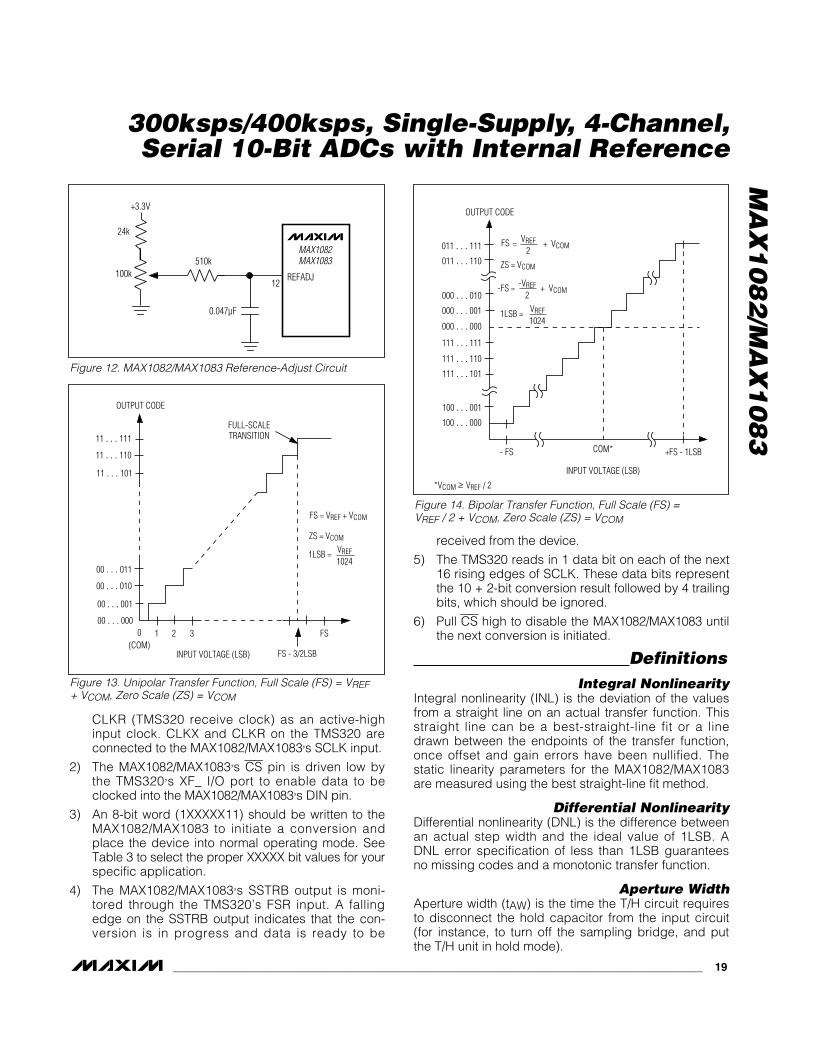
Internal Reference The MAX1082/MAX1083’s full-scale range with theinternal reference is 2.5V with unipolar inputs and±1.25V with bipolar inputs. The internal reference volt-age is adjustable by ±100mV with the circuit in Figure12.
External ReferenceThe MAX1082/MAX1083’s external reference can beplaced at the input (REFADJ) or the output (REF) of theinternal reference-buffer amplifier. The REFADJ inputimpedance is typically 17kΩ. At REF, the DC inputresistance is a minimum of 18kΩ. During conversion, anexternal reference at REF must deliver up to 350µA DCload current and have 10Ω or less output impedance. Ifthe reference has a higher output impedance or isnoisy, bypass it close to the REF pin with a 4.7µFcapacitor.
To use the direct REF input, disable the internal bufferby connecting REFADJ to VDD1. Using the REFADJinput makes buffering the external reference unneces-sary.
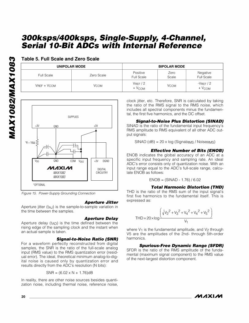
Transfer FunctionTable 5 shows the full-scale voltage ranges for unipolarand bipolar modes.
Figure 13 depicts the nominal, unipolar input/output(I/O) transfer function, and Figure 14 shows the bipolarI/O transfer function. Code transitions occur halfwaybetween successive-integer LSB values. Output codingis binary, with 1LSB = 2.44mV (2.500V/2/1024) for
300ksps/400ksps, Single-Supply, 4-Channel,Serial 10-Bit ADCs with Internal Reference
16 ______________________________________________________________________________________
tCSW
tCP tCSH tCS1
tSTD
tDODtDOV
tDOH
tSTV
tSTH
#10SCLK
DIN
DOUT
SSTRB
tCSS tCH tCSO tCL
tDH
tDOE
tDS
tSTE
CS
Figure 6. Detailed Serial-Interface Timing
MA
X1
08
2/M
AX
10
83
300ksps/400ksps, Single-Supply, 4-Channel,Serial 10-Bit ADCs with Internal Reference
______________________________________________________________________________________ 17
SCLK
1 1 158 8 5 812 12 1216 16 1 516
B4B9S0B4B9S0
DIN
SSTRB
DOUT
CS
CONTROL BYTE 0S S SCONTROL BYTE 1
CONVERSION RESULT 1CONVERSION RESULT 0
CONTROL BYTE 2 S ETC
B4B9
Figure 7. Continuous 16-Clock/Conversion Timing
0
0.50
0.25
1.00
0.75
1.25
1.50
0.0001 0.010.001 0.1 1 10TIME IN SHUTDOWN (s)
REFE
RENC
E PO
WER
-UP
DELA
Y (m
s)
MAX1083, VDD1 = VDD2 = 3.0V CLOAD = 20pFCODE = 1010100000
1000
100
10
10.1 101 100 1k 10k
SAMPLING RATE (sps)
SUPP
LY C
URRE
NT (µ
A)
4 CHANNELS
1 CHANNEL
10,000
1000
10
100
11 10010 1k 10k 100k
SAMPLING RATE (sps)
SUPP
LY C
URRE
NT (µ
A)MAX1083, VDD1 = VDD 2= 3.0V CLOAD = 20pFCODE = 1010100000
4 CHANNELS
1 CHANNEL
Figure 8. Reference Power-Up Delay vs. Time in Shutdown
Figure 9a. Average Supply Current vs. Conversion Rate withInternal Reference in FULLPD
Figure 9b. Average Supply Current vs. Conversion Rate withExternal Reference in FULLPD
2.5
2.0
1.0
1.5
0.50 150 25010050 200 300 350
SAMPLING RATE (sps)
SUPP
LY C
URRE
NT (m
A)
MAX1083, VDD1 = VDD2 = 3.0V CLOAD = 20pFCODE = 1010100000
REDPFASTPD
NORMAL OPERATION
Figure 10. Average Supply Current vs. Sampling Rate (inFASTPD, REDP, and Normal Operation)
MA
X1
08
2/M
AX
10
83
300ksps/400ksps, Single-Supply, 4-Channel,Serial 10-Bit ADCs with Internal Reference
18 ______________________________________________________________________________________
Figure 11a. Full Power-Down Timing
REFADJ1.22V
1.22V0V
2.5mA 2.5mA1.3mA OR 0.9mA
DIN
IVDD1 + IVDD2
REF
FULLPD REDP
WAIT 1.2ms (7 x RC)
FULLPD
1 0 0 1 1
γ = RC = 17kΩ x 0.01µF
DUMMY CONVERSION
11 0 0 0
2.5V
2.5mA
0mA 0mA
2.5V0V
Figure 11b. FASTPD and REDP Timing
2.5V (ALWAYS ON)
2.5mA 2.5mA
DIN
IVDD1 + IVDD2
REF
REDP REDP FASTPD
1 1 0 1 11 0 0 1
2.5mA
0.9mA 0.9mA 1.3mA
unipolar operation, and 1LSB = 2.44mV [(2.500V / 2) /1024] for bipolar operation.
Layout, Grounding, and BypassingFor best performance, use printed circuit (PC) boards;wire-wrap boards are not recommended. Board layoutshould ensure that digital and analog signal lines areseparated from each other. Do not run analog and digi-tal (especially clock) lines parallel to one another, ordigital lines underneath the ADC package.
Figure 15 shows the recommended system groundconnections. Establish a single-point analog ground(star ground point) at GND. Connect all other analoggrounds to the star ground. Connect the digital systemground to this ground only at this point. For lowest-noise operation, the ground return to the star ground’spower supply should be low impedance and as shortas possible.
High-frequency noise in the VDD1 power supply mayaffect the high-speed comparator in the ADC. Bypassthe supply to the star ground with 0.1µF and 10µF
capacitors close to VDD1 of the MAX1082/MAX1083.Minimize capacitor lead lengths for best supply-noiserejection. If the power supply is very noisy, a 10Ω resis-tor can be connected as a lowpass filter (Figure 15).
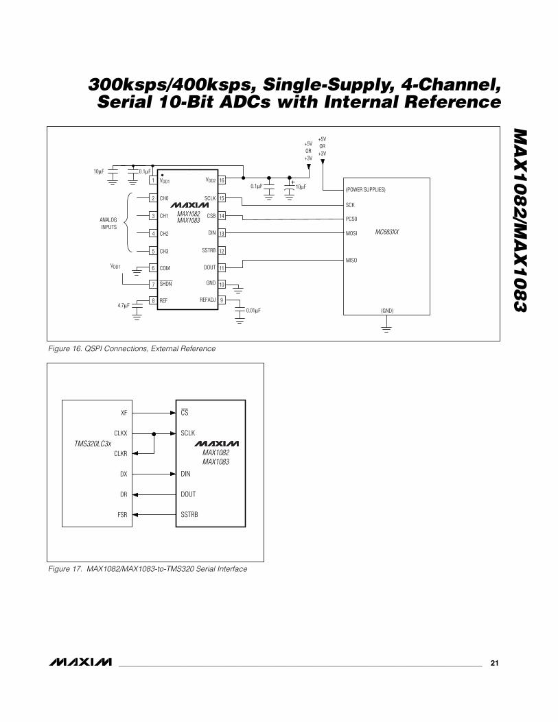
High-Speed Digital Interfacing with QSPIThe MAX1082/MAX1083 can interface with QSPI using the circuit in Figure 16 (CPOL = 0, CPHA = 0). This QSPIcircuit can be programmed to do a conversion on each ofthe four channels. The result is stored in memory withouttaxing the CPU, since QSPI incorporates its own microse-quencer.
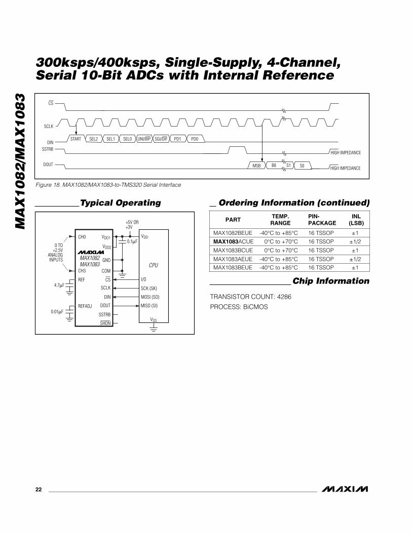
TMS320LC3x Interface Figure 17 shows an application circuit to interface theMAX1082/MAX1083 to the TMS320 in external clockmode. The timing diagram for this interface circuit isshown in Figure 18.
Use the following steps to initiate a conversion in theMAX1082/MAX1083 and to read the results:
1) The TMS320 should be configured with CLKX(transmit clock) as an active-high output clock and
MA
X1
08
2/M
AX
10
83
300ksps/400ksps, Single-Supply, 4-Channel,Serial 10-Bit ADCs with Internal Reference
______________________________________________________________________________________ 19
CLKR (TMS320 receive clock) as an active-highinput clock. CLKX and CLKR on the TMS320 areconnected to the MAX1082/MAX1083’s SCLK input.
2) The MAX1082/MAX1083’s CS pin is driven low bythe TMS320’s XF_ I/O port to enable data to beclocked into the MAX1082/MAX1083’s DIN pin.
3) An 8-bit word (1XXXXX11) should be written to theMAX1082/MAX1083 to initiate a conversion andplace the device into normal operating mode. SeeTable 3 to select the proper XXXXX bit values for yourspecific application.
4) The MAX1082/MAX1083’s SSTRB output is moni-tored through the TMS320’s FSR input. A fallingedge on the SSTRB output indicates that the con-version is in progress and data is ready to be
received from the device.
5) The TMS320 reads in 1 data bit on each of the next16 rising edges of SCLK. These data bits representthe 10 + 2-bit conversion result followed by 4 trailingbits, which should be ignored.
6) Pull CS high to disable the MAX1082/MAX1083 untilthe next conversion is initiated.
DefinitionsIntegral Nonlinearity
Integral nonlinearity (INL) is the deviation of the valuesfrom a straight line on an actual transfer function. Thisstraight line can be a best-straight-line fit or a linedrawn between the endpoints of the transfer function,once offset and gain errors have been nullified. Thestatic linearity parameters for the MAX1082/MAX1083are measured using the best straight-line fit method.
Differential NonlinearityDifferential nonlinearity (DNL) is the difference betweenan actual step width and the ideal value of 1LSB. ADNL error specification of less than 1LSB guaranteesno missing codes and a monotonic transfer function.
Aperture WidthAperture width (tAW) is the time the T/H circuit requiresto disconnect the hold capacitor from the input circuit(for instance, to turn off the sampling bridge, and putthe T/H unit in hold mode).
+3.3V
510k
24k
100k
0.047µF
12REFADJ
MAX1082MAX1083
Figure 12. MAX1082/MAX1083 Reference-Adjust Circuit
OUTPUT CODE
FULL-SCALETRANSITION11 . . . 111
11 . . . 110
11 . . . 101
00 . . . 011
00 . . . 010
00 . . . 001
00 . . . 0001 2 30
(COM)FS
FS - 3/2LSB
FS = VREF + VCOM
ZS = VCOM
INPUT VOLTAGE (LSB)
1LSB = VREF 1024
Figure 13. Unipolar Transfer Function, Full Scale (FS) = VREF+ VCOM, Zero Scale (ZS) = VCOM
011 . . . 111
011 . . . 110
000 . . . 010
000 . . . 001
000 . . . 000
111 . . . 111
111 . . . 110
111 . . . 101
100 . . . 001
100 . . . 000
- FS COM*
INPUT VOLTAGE (LSB)
OUTPUT CODE
ZS = VCOM
+FS - 1LSB
*VCOM VREF / 2
+ VCOM FS = VREF 2
-FS = + VCOM -VREF 2
1LSB = VREF 1024
≤
Figure 14. Bipolar Transfer Function, Full Scale (FS) = VREF / 2 + VCOM, Zero Scale (ZS) = VCOM
MA
X1
08
2/M
AX
10
83
300ksps/400ksps, Single-Supply, 4-Channel,Serial 10-Bit ADCs with Internal Reference
20 ______________________________________________________________________________________
UNIPOLAR MODE BIPOLAR MODE
Full Scale Zero Scale Positive Zero Negative
Full Scale Scale Full Scale
VREF + VCOM VCOMVREF / 2
VCOM-VREF / 2
+ VCOM + VCOM
Table 5. Full Scale and Zero Scale
Aperture JitterAperture jitter (tAJ) is the sample-to-sample variation inthe time between the samples.
Aperture DelayAperture delay (tAD) is the time defined between therising edge of the sampling clock and the instant whenan actual sample is taken.
Signal-to-Noise Ratio (SNR)For a waveform perfectly reconstructed from digitalsamples, the SNR is the ratio of the full-scale analoginput (RMS value) to the RMS quantization error (resid-ual error). The ideal, theoretical minimum analog-to-dig-ital noise is caused only by quantization error andresults directly from the ADC’s resolution (N bits):
SNR = (6.02 x N + 1.76)dB
In reality, there are other noise sources besides quanti-zation noise, including thermal noise, reference noise,
clock jitter, etc. Therefore, SNR is calculated by takingthe ratio of the RMS signal to the RMS noise, whichincludes all spectral components minus the fundamen-tal, the first five harmonics, and the DC offset.
Signal-to-Noise Plus Distortion (SINAD)SINAD is the ratio of the fundamental input frequency’sRMS amplitude to RMS equivalent of all other ADC out-put signals:
SINAD (dB) = 20 x log (SignalRMS / NoiseRMS)
Effective Number of Bits (ENOB)ENOB indicates the global accuracy of an ADC at aspecific input frequency and sampling rate. An idealADC’s error consists only of quantization noise. With aninput range equal to the ADC’s full-scale range, calcu-late ENOB as follows:
ENOB = (SINAD - 1.76) / 6.02
Total Harmonic Distortion (THD)THD is the ratio of the RMS sum of the input signal’sfirst five harmonics to the fundamental itself. This isexpressed as:
where V1 is the fundamental amplitude, and V2 throughV5 are the amplitudes of the 2nd- through 5th-orderharmonics.
Spurious-Free Dynamic Range (SFDR)SFDR is the ratio of the RMS amplitude of the funda-mental (maximum signal component) to the RMS valueof the next-largest distortion component.
THD 20 logV V V V V
V
22
32
42
42
52
1= ×
+ + + +
+3V +3V
SUPPLIES
DGND+3VVDD2COMGNDVDD
DIGITALCIRCUITRYMAX1082
MAX1083
*R = 10Ω
*OPTIONAL
GND
Figure 15. Power-Supply Grounding Connection
MA
X1
08
2/M
AX
10
83
300ksps/400ksps, Single-Supply, 4-Channel,Serial 10-Bit ADCs with Internal Reference
______________________________________________________________________________________ 21
MC683XX
(POWER SUPPLIES)
SCK
PCS0
MOSI
MISO
0.1µF 10µF
(GND)0.01µF4.7µF
ANALOG INPUTS
+5VOR+3V
+5VOR+3V
16
15
14
13
12
11
10
9
1
2
3
4
5
6
7
8
MAX1082MAX1083
VDD2
SCLK
CSB
DIN
SSTRB
DOUT
GND
REFADJ
VDD1
CH0
CH1
COM
CH2
CH3
SHDN
REF
10µF 0.1µF
VDD1
Figure 16. QSPI Connections, External Reference
XF
CLKX
CLKR
DX
DR
FSR
CS
SCLK
DIN
DOUT
SSTRB
TMS320LC3xMAX1082MAX1083
Figure 17. MAX1082/MAX1083-to-TMS320 Serial Interface
MA
X1
08
2/M
AX
10
83
300ksps/400ksps, Single-Supply, 4-Channel,Serial 10-Bit ADCs with Internal Reference
22 ______________________________________________________________________________________
SCLK
DIN
DOUT
SSTRB
SEL2START SEL1 SEL0 PD1 PD0
CS
UNI/BIP SGI/DIF
B8 S1MSB S0
HIGH IMPEDANCE
HIGH IMPEDANCE
Figure 18. MAX1082/MAX1083-to-TMS320 Serial Interface
PARTTEMP. RANGE
PIN-PACKAGE
MAX1082BEUE
MAX1083AEUE
MAX1083BEUE -40°C to +85°C
-40°C to +85°C
-40°C to +85°C 16 TSSOP
16 TSSOP
16 TSSOP
±1
±1/2
INL(LSB)
±1
MAX1083ACUE
MAX1083BCUE 0°C to +70°C
0°C to +70°C 16 TSSOP
16 TSSOP
±1/2
±1
Ordering Information (continued)Typical Operating
VDD
I/O
SCK (SK)
MOSI (SO)
MISO (SI)
VSSSHDN
SSTRB
DOUT
DIN
SCLK
CS
COM
GND
VDD1
VDD2
CH3
4.7µF
0.1µFCH0
0 TO+2.5V
ANALOGINPUTS MAX1082
MAX1083 CPU
+5V OR +3V
REF
0.01µFREFADJ
Chip Information
TRANSISTOR COUNT: 4286
PROCESS: BiCMOS
MA
X1
08
2/M
AX
10
83
300ksps/400ksps, Single-Supply, 4-Channel,Serial 10-Bit ADCs with Internal Reference
______________________________________________________________________________________ 23
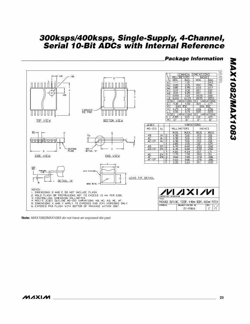
________________________________________________________Package Information
TSS
OP
.EP
SNote: MAX1082/MAX1083 do not have an exposed die pad.

MA
X1
08
2/M
AX
10
83
300ksps/400ksps, Single-Supply, 4-Channel,Serial 10-Bit ADCs with Internal Reference
Maxim cannot assume responsibility for use of any circuitry other than circuitry entirely embodied in a Maxim product. No circuit patent licenses areimplied. Maxim reserves the right to change the circuitry and specifications without notice at any time.
24 ____________________Maxim Integrated Products, 120 San Gabriel Drive, Sunnyvale, CA 94086 408-737-7600
© 2000 Maxim Integrated Products Printed USA is a registered trademark of Maxim Integrated Products.
NOTES