Embed Size (px)
Citation preview

3 PROGRAM SEQUENCERFigure 3-0.
Table 3-0.
Listing 3-0.
OverviewThis chapter describes the program sequencer of the ADSP-218x family processors. The program sequencer circuitry controls the flow of program execution. It contains an interrupt controller and status and condition logic.
The program sequencer generates a stream of instruction addresses and provides flexible control of program flow. It allows sequential instruction execution, zero-overhead looping, sophisticated interrupt servicing, and single-cycle branching with jumps and calls (both conditional and unconditional).
This chapter discusses each function on the program sequencer. It also dis-cusses both the program sequencer logic and the following instructions used to control program flow:
• DO UNTIL
• JUMP
• CALL
• RTS (Return from Subroutine)
• RTI (Return from Interrupt)
• IDLE
For a complete description of each instruction, refer to the ADSP-218x DSP Instruction Set Reference.
ADSP-218x DSP Hardware Reference 3-1

Program Sequencer Structure
Program Sequencer StructureFigure 3-1 shows a block diagram of the program sequencer.
INTERRUPT
CONTROLLE R
CONDITIONLOGIC
LOOP STACK
DM D BUS
NEXTADDRESSSOURCESELECT
INCREM ENT
PROGRAMCOUNTER
NEXT ADDRESS MUX
PCSTACK
PM A BUS
M UX
STATUS
REGISTERS
STATUSSTACK
COUNTSTACK
CNTR(COUNTER)CE OUT
CONDITION CODE
ADDRESS OF JUM P/CALL
FUNCTION FIELD
ADDRESS OF LAST INSTRUCTION IN LOOP
&TERM INATION
CONDITION
FROM INSTRUCTION REGISTER
LOOPCOM PARATOR
ARITHM ETICSTATUS
(from ALU)
INTERRUPTS
M UX
M UX
fromFI Pin
Figure 3-1. Program Sequencer Block Diagram
3-2 ADSP-218x DSP Hardware Reference

Program Sequencer
The sections that follow describe the functions shown in the diagram in detail.
Next Address Select LogicWhile the processor is executing an instruction, the program sequencer prefetches the next instruction. The sequencer’s next address select logic generates a program memory address (for the prefetch) from one of four sources:
• Program Counter (PC) incrementer
• PC stack
• Instruction register
• Interrupt controller
The next address circuit (shown in Figure 3-1) selects which of these sources is used, based on inputs from the Instruction register, condition logic, loop comparator and interrupt controller. The next instruction address is then output on the PMA bus for the prefetch.
The PC incrementer is selected as the source of the next address if program flow is sequential. This is also the case when a conditional jump or return is not taken and when a DO UNTIL loop terminates. The output of the PC incrementer is driven onto the PMA bus and is loaded back into the pro-gram counter to begin the next cycle.
The PC stack is used as the source for the next address when a return from subroutine or return from interrupt is executed. The top stack value is also used as the next address when returning to the top of a DO UNTIL loop.
The Instruction register provides the next address when a direct jump is taken. The 14-bit jump address is embedded in the instruction word.
ADSP-218x DSP Hardware Reference 3-3

Program Sequencer Structure
The interrupt controller provides the next program memory address when servicing an interrupt. Upon recognizing a valid interrupt, the processor jumps to the interrupt vector location corresponding to the active inter-rupt request.
Another possible source for the next address is one of the I4-I7 index reg-isters of DAG2 (Data Address Generator 2), used when a register indirect jump is executed, as shown in the following instruction:
JUMP (I4);
In this example, the PC is loaded from DAG2 via the PMA bus. (See Chapter 4, “Data Address Generators” for detailed information about the data address generators.)
Program Counter Register and StackThe PC is a 14-bit register that always contains the address of the currently executing instruction. The output of the PC is fed into a 14-bit incre-menter, which adds 1 to the current PC value. The output of the incrementer can be selected by the next address multiplexer to fetch the next sequential instruction.
Associated with the PC is a 14-bit by 16-word stack that is pushed with the output of the incrementer when a CALL instruction is executed. The PC stack is also pushed when a DO UNTIL is executed and when an interrupt is processed. For interrupts, however, the incrementer is disabled so that the current PC value (instead of PC+1) is pushed. This allows the current instruction, which is aborted, to be refetched upon returning from the interrupt service routine. The pushing and popping of the PC stack occurs automatically in all of these cases. The stack can also be manually popped with the POP instruction.
A special instruction is provided for reading (popping) or writing (push-ing) the top value of the PC stack. This instruction uses the pseudo register TOPPCSTACK, described at the end of this chapter.
3-4 ADSP-218x DSP Hardware Reference

Program Sequencer
The output of the next address multiplexer is fed back to the PC, which normally reloads it at the end of each processor cycle. In the case of a reg-ister indirect jump, however, DAG2 drives the PMA bus with the next instruction address and the PC is loaded directly from the PMA bus.
Loop Counter Register and StackThe counter and count stack provide the program sequencer with a pow-erful looping mechanism. The counter is a 14-bit register with automatic post-decrement capability that controls the flow of program loops, which execute a predetermined number of times. Count values are 14-bit unsigned-magnitude values.
Before entering the loop, the counter register (CNTR) is loaded with the desired loop count from the lower 14 bits of the DMD bus. The actual loop count N is loaded, as opposed to N–1. This is due to the operation of the counter expired (CE) status logic, which tests CE (and automatically post-decrements the counter) at the end of a DO UNTIL loop that uses CE as its termination condition. CE is tested at the beginning of each processor cycle and the counter is decremented at the end; therefore CE is asserted when the counter reaches 1 so that the loop executes N times.
The counter may also be tested and automatically decremented by a con-ditional jump instruction that tests NOT CE. The counter is not decremented when NOT CE is checked as part of a conditional return or conditional arithmetic instruction.
The counter may be read directly over the DMD bus at any time without affecting its contents. When reading the counter, the upper two bits of the DMD bus are padded with zeroes.
ADSP-218x DSP Hardware Reference 3-5

Program Sequencer Structure
The count stack is a 14-bit by 4-word stack that allows nesting of loops by storing temporarily dormant loop counts. When a new value is loaded into the counter from the DMD bus, the current counter value is auto-matically pushed onto the count stack. The count stack is automatically popped whenever the CE status is tested and is true, thereby resuming exe-cution of the outer loop (if any). The count stack may also be popped manually if an early exit from a loop is taken.
There are two exceptions to the automatic pushing of the count stack. A counter load from the DMD bus does not cause a count stack push if there is no valid value in the counter, because a stack location would be wasted on the invalid counter value. There is no valid value in the counter after a system reset and also after the CE condition is tested when the count stack is empty. The count stack empty status bit in the SSTAT register indi-cates when the stack is empty.
The second exception is provided explicitly by the special purpose syntax OWRCNTR (overwrite counter). Writing a value to OWRCNTR overwrites the counter with the new value, and nothing is pushed onto the count stack. OWRCNTR cannot be read (i.e. used as a source register) and must not be written in the last instruction of a DO UNTIL loop.
Loop Comparator and StackThe DO UNTIL instruction initiates a zero-overhead loop using the loop comparator and loop stack of the program sequencer.
On every processor cycle, the loop comparator compares the next address generated by the program sequencer to the address of the last instruction of the loop (which is embedded in the DO UNTIL instruction). The address of the first instruction in the loop is maintained on the top of the PC stack. When the last instruction in the loop is executed the processor con-ditionally jumps to the beginning of the loop, eliminating the branching overhead otherwise incurred in loop execution.
3-6 ADSP-218x DSP Hardware Reference

Program Sequencer
The loop stack stores the last instruction addresses and termination condi-tions of temporarily dormant loops. Up to four levels can be stored. The only extra cycle associated with the nesting of DO UNTIL loops is the execu-tion of the DO UNTIL instruction itself, since the pushing and popping of all stacks associated with the looping hardware is automatic.
When using the counter expired (CE) status as the termination condition for the loop, an additional cycle is required for the initial loading of the counter. Table 3-1 shows the termination conditions that can be used with DO UNTIL.
Table 3-1. DO UNTIL Termination Condition Logic
Syntax Status Condition True If:
EQ Equal Zero AZ = 1
NE Not Equal Zero AZ = 0
LT Less Than Zero AN .XOR. AV = 1
GE Greater Than or Equal Zero AN .XOR. AV = 0
LE Less Than or Equal Zero (AN .XOR. AV) .OR. AZ = 1
GT Greater Than Zero (AN .XOR. AV) .OR. AZ = 0
AC ALU Carry AC = 1
NOT AC Not ALU Carry AC = 0
AV ALU Overflow AV = 1
NOT AV Not ALU Overflow AV = 0
MV MAC Overflow MV = 1
NOT MV Not MAC Overflow MV = 0
ADSP-218x DSP Hardware Reference 3-7

Program Sequencer Structure
When a DO UNTIL instruction is executed, the 14-bit address of the last instruction and a 4-bit termination condition (both contained in the DO UNTIL instruction) are pushed onto the 18-bit by 4-word loop stack. Simultaneously, the PC incrementer output is pushed onto the PC stack. Since the DO UNTIL instruction is located just before the first instruction of the loop, the PC stack then contains the first loop instruction address, and the loop stack contains the last loop instruction address and termination condition. The non-empty state of the loop stack activates the loop com-parator which compares the address on top of the loop stack with the address of the next instruction. When these two addresses are equal, the loop comparator notifies the next address source selector that the last instruction in the loop will be executed on the next cycle.
At this point, there are three possible results depending on the type of instruction at the end of the loop. Case 1 illustrates the most typical situa-tion. Cases 2 and 3 are also allowed but involve greater program complexity for proper execution.
NEG X Input Sign Negative AS = 1
POS X Input Sign Positive AS = 0
CE Counter Expired
FOREVER Always
Table 3-1. DO UNTIL Termination Condition Logic (Cont’d)
Syntax Status Condition True If:
3-8 ADSP-218x DSP Hardware Reference

Program Sequencer
Case 1—Last instruction in loop IS NOT a program flow instruction
If the last instruction in the loop is not a jump, call, return, or idle, the next address circuit will select the next address based on the termination condition stored on the top of the loop stack. If the condition is false, the top address on the PC stack is selected, causing a fetch of the first instruc-tion of the loop. If the termination condition is true, the PC incrementer is chosen, causing execution to fall out of the loop. The loop stack, PC stack, and counter stack (if being used) are then popped.
! Conditional arithmetic instructions execute based on the condition explicitly stated in the instruction, whereas the loop sequencing is controlled by the (implicit) termination condition contained on top of the stack.
Case 2—Last instruction in loop IS a program flow instruction
If the last instruction in the loop is a jump, call, or return, the explicitly stated instruction takes precedence over the implicit sequencing of the loop. If the condition in the instruction is false, normal loop sequencing takes place as described for Case 1.
If the condition in the instruction is true, however, program control trans-fers to the jump/call/return address. Any actions that would normally occur upon an end-of-loop detection do not take place: fetching the first instruction of the loop, falling out of the loop and popping the loop stack, PC stack, and counter stack, or decrementing the counter.
! For a return instruction, control is passed back to the top of the loop since the PC stack contains the beginning address of the loop.
ADSP-218x DSP Hardware Reference 3-9

Program Sequencer Structure
Case 3—Last instruction in loop is an IDLE instruction
If the last instruction in the loop is an IDLE, program flow is controlled by the IDLE instruction rather than the loop. When the IDLE instruction is executed, the processor enters a low-power wait-for-interrupt state. When the processor is interrupted, loop execution terminates and program exe-cution continues with the first instruction following the loop.
" Caution is required when ending a loop with a JUMP, CALL, RETURN, or IDLE instruction, or when making a premature exit from a loop. Since none of the loop sequencing mechanisms are active while the jump/call/return is being performed, the loop, PC, and counter stacks are left with the looping information (since they are not popped).
In this situation, a manual pop of each of the relevant stacks is required to restore the correct state of the processor. A subroutine call poses this problem only when it is the last instruction in a loop; in such cases, the return causes program flow to transfer to the instruction just after the loop. Calls within a loop that are not the last instruction operate as in Case 1.
The only restriction concerning DO UNTIL loops is that nested loops cannot terminate on the same instruction. Since the loop comparator can only check for one loop termination at a time, falling out of an inner loop by incrementing the PC would go beyond the end address of the outer loop if they terminated on the same instruction.
! The do-loop hardware has no knowledge of the PMOVLAY register. Therefore, the do-loop hardware controls the program flow when-ever the PC reaches the end-of-loop address, no matter which PM Overlay page the program is running.
3-10 ADSP-218x DSP Hardware Reference

Program Sequencer
Program Control InstructionsThe following sections describe the primary instructions used to control program flow.
JUMP InstructionThe ADSP-218x processors have two types of JUMP instructions: direct JUMP instruction and register indirect JUMP instructions.
Direct JUMP Instructions
In direct JUMP instructions, the 14-bit jump address is embedded in the JUMP instruction word. When a direct JUMP instruction is decoded, the jump address is input directly to the next address MUX of the program sequencer. The address is driven onto the PMA bus and fed back to the PC for the next cycle. For example, the instruction
JUMP fir_start;
jumps to the address of the label fir_start.
Register Indirect JUMP Instructions
In register indirect JUMP instructions, the jump address is supplied by one of the I registers of DAG2 (I4, I5, I6, or I7). (See Chapter 4, “Data Address Generators” for a full description of the data address generators.) The address is driven onto the PMA bus by DAG2 and is loaded into the PC on the next cycle. For example, the instruction
JUMP (I4);
will jump to the address contained in the I4 register.
ADSP-218x DSP Hardware Reference 3-11

Program Control Instructions
The indirect JUMP instruction can be a cycle-saving alternative to hardware loops since the jump takes only a single cycle instead of the two the do-loop hardware setup requires. Listing 3-1 and Listing 3-2 illustrate how you can substitute an indirect JUMP instruction for a nested loop. In this example, the indirect JUMP instruction is substituted for nested loops with a high count outer loop and a variable low-count inner loop that contains only a few instructions.
Listing 3-1. Nested Loop
CNTR = 10000;do outer_loop until ce;
...CNTR = DM(mycounter); /* values between 1 and 2^16 –1
allowed */do inner_loop until ce;
inner_loop: <instr_a>;<instr_b>...
outer_loop: <instr_x>
Listing 3-2. Indirect JUMP
ay0 = DM(mycounter); /* only values between 0 and 4allowed */
ar = inner_loop;ar = ar – ay0;i4 = ar;
CNTR = 10000;do outer_loop until ce;
...jump (i4);<instr_a>;<instr_a>;<instr_a>;<instr_a>;
inner_loop: <instr_b>...
outer_loop: <instr_x>
3-12 ADSP-218x DSP Hardware Reference

Program Sequencer
CALL InstructionThe CALL instruction executes in a similar fashion to the JUMP instruction. The address of the subroutine is embedded in the CALL instruction word and, once extracted from the instruction register, is fed back the PC for the next cycle. In addition, the current value of the program counter is incre-mented and pushed onto the PC stack. Upon return from the subroutine, the PC stack is popped into the program counter and execution resumes with the instruction following the CALL.
DO UNTIL LoopsThe most common form of a DO UNTIL loop uses the counter register as a loop iteration counter. When the counter is used to control loop iteration, counter expired (CE) must be used as the DO UNTIL termination condition. A simple example of this type of loop is shown in Listing 3-3.
Listing 3-3. DO UNTIL Loop Example
L0=10; /* setup circular buffer length *//* register */
I0=data_buffer; /* load pointer with first address */ /* of circular buffer */
M0=1; /* setup modify register for pointer *//* increment */
CNTR=10; /* load counter with circular buffer */ /* length */ DO loop UNTIL CE; /* repeat loop until counter expired */ DM(I0,M0)=0; /* initialize/clear circular buffer */ ...any instruction...loop: ...any instruction...
ADSP-218x DSP Hardware Reference 3-13

Program Control Instructions
When the
CNTR=10;
instruction is executed, prior to entering the loop, the counter is loaded via the DMD bus. Any previously existing count would be simultaneously pushed onto the count stack; this push operation is omitted if the counter is empty. The
DO loop UNTIL CE;
instruction itself only sets up the conditions for looping; no other opera-tion occurs while the instruction is executed. This occurs only once, at the beginning of the first time through the loop.
Execution of the DO UNTIL instruction pushes the address of the instruc-tion immediately following the DO UNTIL onto the PC stack (by pushing the incremented PC). On the same cycle, the loop stack is pushed with the address of the end-of-loop instruction and the termination condition.
As execution continues within the loop, the loop comparator checks each instruction’s address against the address of the loop’s last instruction. Until that address is reached, normal execution continues.
Each time the end of the loop is reached, the loop comparator determines that the currently executing instruction is the last in the loop. This affects the next address select logic of the program sequencer: instead of using the incremented PC for the next address, the loop termination condition is evaluated. If the termination condition is false, execution continues with the first instruction of the loop (the top of the PC stack is taken as the next address). Note that the PC and loop stacks are not popped, only read.
3-14 ADSP-218x DSP Hardware Reference

Program Sequencer
On the final pass through the loop, the termination condition is true. The PC stack is popped and execution continues with the instruction immedi-ately following the last instruction of the loop. The loop stack and count stack are also popped on this cycle.
! The do-loop hardware tests CE at the end of the loop only. When CNTR is programmed to zero, the loop is repeated 214 times.
IDLE InstructionThe IDLE instruction causes the processor to wait indefinitely in a low power state until an interrupt occurs. When an unmasked interrupt occurs, it is serviced; execution then continues with the instruction fol-lowing the IDLE instruction.
Slow IDLE Instruction
An enhanced version of the IDLE instruction allows the processor’s inter-nal clock signal to be slowed, further reducing power consumption. The reduced clock frequency, a programmable fraction of the normal clock rate, is specified by a selectable divisor given in the IDLE instruction. The format of the instruction is
IDLE (n);
where n = 16, 32, 64, or 128. This instruction keeps the processor fully functional, but operating at the slower clock rate. While it is in this state, the processor’s other internal clock signals, such as SCLK, CLKOUT, and timer clock, are reduced by the same ratio. The default form of the instruction, when no clock divisor is given, is the standard IDLE instruction.
ADSP-218x DSP Hardware Reference 3-15

Interrupts
When the IDLE (n) instruction is used, it effectively slows down the pro-cessor’s internal clock and thus its response time to incoming interrupts. The interrupt response time is increased because the instruction cycle is extended by the clock divisor n. When an enabled interrupt is received, the processor will remain in the idle state for up to a maximum of n pro-cessor cycles before resuming normal operation (n = 16, 32, 64, or 128).
When the IDLE (n) instruction is used in systems that have an externally generated serial clock (SCLK), the serial clock rate may be faster than the processor’s reduced internal clock rate. Under these conditions, interrupts must not be generated at a faster rate than can be serviced, due to the additional time the processor takes to come out of the idle state (a maxi-mum of n processor cycles).
InterruptsThe program sequencer’s interrupt controller responds to interrupts by shifting control to the instruction located at the appropriate interrupt vec-tor address. Table 3-2 shows the interrupts and associated vector addresses for the ADSP-218x family processors.
! SPORT1 can be configured as either a serial port or as a collection of control pins, including two external interrupt inputs, IRQ0 and IRQ1. See Chapter 5, “Serial Ports” for more information about the configuration of SPORT1.
Table 3-2. ADSP-218x Interrupts & Interrupt Vector Addresses
Interrupt Source Interrupt Vector Address
RESET startup (or powerup w/PUCR=1) 0x0000 (highest priority)
Powerdown (non-maskable) 0x002C
IRQ2 0x0004
3-16 ADSP-218x DSP Hardware Reference

Program Sequencer
The interrupt vector locations are spaced four program memory locations apart—this allows short interrupt service routines to be coded in place, with no jump to the service routine required. For interrupt service rou-tines with more than four instructions, however, program control must be transferred to the service routine by means of a jump instruction placed at the interrupt vector location.
After an interrupt has been serviced, an RTI (Return From Interrupt) instruction returns control to the main program by popping the top value on the PC stack into the PC; the status stack is also popped to restore the previous processor state.
Interrupts can also be forced under software control; see the discussion of the IFC register in the section“Configuring Interrupts”.
IRQL1 (level-sensitive) 0x0008
IRQL0 (level-sensitive) 0x000C
SPORT0 Transmit 0x0010
SPORT0 Receive 0x0014
IRQE (edge-sensitive) 0x0018
Byte DMA Interrupt 0x001C
SPORT1 Transmit or IRQ1 0x0020
SPORT1 Receive or IRQ0 0x0024
Timer 0x0028 (lowest priority)
Table 3-2. ADSP-218x Interrupts & Interrupt Vector Addresses (Cont’d)
Interrupt Source Interrupt Vector Address
ADSP-218x DSP Hardware Reference 3-17

Interrupts
Because of the efficient stack and program sequencer, there is no latency (beyond synchronization delay) when processing unmasked interrupts, even when interrupting DO UNTIL loops. Nesting of interrupts allows higher-priority interrupts to interrupt any lower-priority interrupt service routines that may currently be executing, also with no additional latency.
The ADSP-218x family processors include a secondary register set which can be used to provide a fresh set of ALU, MAC, and Shifter registers dur-ing interrupt servicing. This feature allows single-cycle context switching. Use of the secondary registers is described in the section, “Mode Status Register” on page 3-30.
Interrupt Servicing SequenceWhen an interrupt request occurs, it is latched while the processor finishes executing the current instruction. The interrupt request is then compared with the interrupt mask (IMASK) register by the interrupt controller.
If the interrupt is not masked, the program sequencer pushes the current value of the program counter (which contains the address of the next instruction) onto the PC stack—this allows execution to continue with the next instruction of the main program after the interrupt is serviced. The program sequencer also pushes the current values of the ASTAT, MSTAT, and IMASK registers onto the status stack. ASTAT, MSTAT, and IMASK are stored in this order, with the MSB of ASTAT first, and so on. When IMASK is pushed, it is automatically reloaded with a new value that determines whether or not interrupt nesting is allowed (based on the value of the interrupt nesting enable bit in ICNTL).
The processor then executes a NOP while simultaneously fetching the instruction located at the interrupt vector address. Upon return from the interrupt service routine, the PC and status stacks are popped and execu-tion resumes with the next instruction of the main program.
3-18 ADSP-218x DSP Hardware Reference

Program Sequencer
Configuring InterruptsThe following registers are used to configure interrupts:
• ICNTL—Determines whether interrupts can be nested and config-ures the external interrupts IRQ2, IRQ1, IRQ0 as edge-sensitive or level-sensitive.
• IMASK—Enables or disables (i.e. masks) each individual interrupt (both external and internal).
• IFC—Forces an interrupt or clears a pending edge-sensitive inter-rupt.
The IRQ2, IRQ1, IRQ0 interrupts may be either edge-sensitive or level-sensi-tive, as selected in the ICNTL register. The ADSP-218x family has three additional interrupt pins: IRQE, IRQL1, and IRQL2. The IRQE input is edge-sensitive, while the IRQL1 and IRQL2 inputs are level-sensitive.
For edge-sensitive IRQx interrupts, an interrupt request is latched inter-nally whenever a falling edge (high-to-low transition) occurs at the input pin. The latch remains set until the interrupt is serviced; it is then auto-matically cleared. A pending edge-sensitive interrupt can also be cleared in software by setting the corresponding clear bit in the IFC register.
Edge-sensitive interrupt inputs generally require less external hardware than level-sensitive inputs, and allow signals such as sampling-rate clocks to be used as interrupts.
A level-sensitive interrupt must remain asserted until the interrupt is ser-viced. The interrupting device must then deassert the interrupt request so that the interrupt is not serviced again. Level-sensitive inputs, however, allow many interrupt sources to use the same input by combining them logically to produce a single interrupt request. Level-sensitive interrupts are not latched.
ADSP-218x DSP Hardware Reference 3-19
Interrupts
Your program can also determine whether or not interrupts can be nested. In non-nesting mode, all interrupt requests are automatically masked out when an interrupt service routine is entered. In nesting mode, the proces-sor allows higher-priority interrupts to be recognized and serviced.
Interrupt Control Register
The Interrupt Control (ICNTL) register is a 5-bit register that configures the external interrupt requests (IRQx) of each processor. All bits in ICNTL are undefined after a processor reset. The bit definitions for each proces-sor’s ICNTL register are given in Appendix B, “Control/Status Registers”.
ICNTL contains an IRQx sensitivity bit for each external interrupt. The sen-sitivity bits determine whether a given interrupt input is edge- or level-sensitive (0 = level-sensitive, 1 = edge-sensitive). There are no sensi-tivity bits for internally generated interrupts.
The interrupt nesting enable bit (bit 4) in ICNTL determines whether nest-ing of interrupt service routines is allowed.
When the value of ICNTL is changed, there is a one cycle latency before the change in interrupt configuration.
Interrupt Mask Register
Each bit of the Interrupt Mask (IMASK) register enables or disables the ser-vicing of an individual interrupt. Specific bit definitions for each processor’s IMASK register are given in Appendix B, “Control/Status Regis-ters.” The mask bits are positive sense: 0=masked, 1=enabled. IMASK is set to zero upon a processor reset.
On the ADSP-218x family processors, all interrupts are automatically dis-abled for one instruction cycle following the execution of an instruction that modifies IMASK. This does not affect serial port autobuffering or DMA transfers.
3-20 ADSP-218x DSP Hardware Reference

Program Sequencer
If an edge-sensitive interrupt request signal occurs when the interrupt is masked, the request is latched but not serviced; the interrupt can then be recognized in software and serviced later.
The contents of IMASK are automatically pushed onto the status stack when entering an interrupt service routine and popped back when return-ing from the routine. The configuration of IMASK upon entering the interrupt service routine is determined by the interrupt nesting enable bit (bit 4) of ICNTL; it may be altered, though, as part of the interrupt service routine itself.
When nesting is disabled, all interrupt levels are masked automatically (IMASK set to zero) when an interrupt service routine is entered.
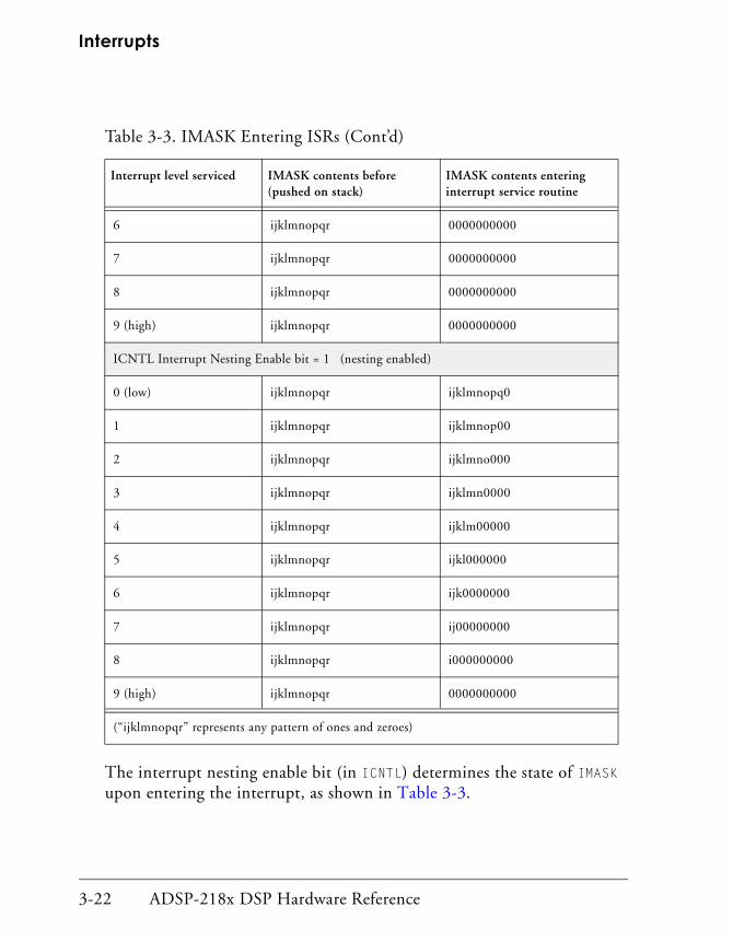
When nesting is enabled, IMASK is set so that only equal and lower priority interrupts are masked; higher priority interrupts remain configured as they were prior to the interrupt. See Table 3-3 for more information.
Table 3-3. IMASK Entering ISRs
Interrupt level serviced IMASK contents before (pushed on stack)
IMASK contents entering interrupt service routine
ICNTL Interrupt Nesting Enable bit = 0 (nesting disabled)
0 (low) ijklmnopqr 0000000000
1 ijklmnopqr 0000000000
2 ijklmnopqr 0000000000
3 ijklmnopqr 0000000000
4 ijklmnopqr 0000000000
5 ijklmnopqr 0000000000
(“ijklmnopqr” represents any pattern of ones and zeroes)
ADSP-218x DSP Hardware Reference 3-21
Interrupts
The interrupt nesting enable bit (in ICNTL) determines the state of IMASK upon entering the interrupt, as shown in Table 3-3.
6 ijklmnopqr 0000000000
7 ijklmnopqr 0000000000
8 ijklmnopqr 0000000000
9 (high) ijklmnopqr 0000000000
ICNTL Interrupt Nesting Enable bit = 1 (nesting enabled)
0 (low) ijklmnopqr ijklmnopq0
1 ijklmnopqr ijklmnop00
2 ijklmnopqr ijklmno000
3 ijklmnopqr ijklmn0000
4 ijklmnopqr ijklm00000
5 ijklmnopqr ijkl000000
6 ijklmnopqr ijk0000000
7 ijklmnopqr ij00000000
8 ijklmnopqr i000000000
9 (high) ijklmnopqr 0000000000
Table 3-3. IMASK Entering ISRs (Cont’d)
Interrupt level serviced IMASK contents before (pushed on stack)
IMASK contents entering interrupt service routine
(“ijklmnopqr” represents any pattern of ones and zeroes)
3-22 ADSP-218x DSP Hardware Reference

Program Sequencer
Global Enable/Disable for Interrupts
Global interrupt enable and disable instructions are available on the ADSP-218x processors:
ENA INTS;DIS INTS;
Interrupts are enabled by default after reset. The DIS INTS instruction causes all interrupts (including powerdown) to be masked out regardless of the contents of IMASK. The ENA INTS instruction allows all unmasked interrupts to be serviced again.
Disabling interrupts does not affect serial port autobuffering or DMA operations.
Interrupt Force and Clear Register
The Interrupt Force and Clear (IFC) register is a write-only register that allows the forcing and clearing of edge-sensitive interrupts in software. An interrupt is forced or cleared under program control by setting the force or clear bit corresponding to the desired interrupt. After the force or clear bit is set, there is one cycle of latency before the interrupt is actually forced or cleared.
Edge-sensitive interrupts can be forced by setting the appropriate force bit in IFC. For most force bit values, programs can load IFC with an immedi-ate 14-bit value, but for the upper bits (14 and 15) a register-to-register load must be used. Setting the force bit causes the interrupt to be serviced once, unless masked. An external interrupt must be edge-sensitive (as determined by ICNTL) to be forced. The timer, SPORT, and IRQE inter-rupts also behave like edge-sensitive interrupts and can be masked, cleared, and forced.
ADSP-218x DSP Hardware Reference 3-23

Interrupts
Pending edge-sensitive interrupts can be cleared by setting the appropriate clear bit in IFC. Edge-triggered interrupts are cleared automatically when the corresponding interrupt service routine is called.
Specific bit definitions for the IFC register are given in Appendix B, “Con-trol/Status Registers”.
! When one of the interrupt pins IRQ0, IRQ1, or IRQ2 is unused and pulled-high, its interrupt functionality is available to implement software interrupts. You must then select edge-sensitivity.
Interrupt Latency
For the timer, IRQx, and SPORT interrupts, latency is at least three full cycles from the time when an interrupt occurs to the time when the first instruction of the service routine is executed. This latency is shown in Figure 3-2. Two cycles are required to synchronize the interrupt inter-nally, assuming that setup and hold times are met (for the IRQx input pins).
Since interrupts are only serviced on instruction boundaries, before execu-tion continues, the instruction(s) executed during these two cycles must be fully completed, including any extra cycles inserted due to Bus Request/Bus Grant or memory wait states.
3-24 ADSP-218x DSP Hardware Reference

Program Sequencer
The third cycle of latency is needed to fetch the first instruction stored at the interrupt vector location. During this cycle, the processor executes a NOP instead of the instruction that would normally have been executed. On the next cycle, execution continues at the first instruction of the inter-rupt service routine. The address of the aborted instruction is pushed onto the PC stack; it will be fetched when the interrupt service routine is completed.
For a pending interrupt that is masked, the latency from execution of the instruction that unmasks the interrupt (in IMASK) to the first instruction of the service routine is one cycle.
CLKOUT
ADDRESS FOR
INSTRUCTIONFETCH
INTERRU PT
INSTRUCTION
EXECUTINGN–2 N–1 N NO P FIRST INST R OF
SERV RO UTINE
N–1 N N+ 1 INTERRUPT
VECTOR II+1
Figure 3-2. Interrupt Latency (Timer, IRQx, and SPORT Interrupts)
ADSP-218x DSP Hardware Reference 3-25

Status Registers and Status Stack
Status Registers and Status StackProcessor status and mode bits are maintained in internal registers which can be independently read from and written to over the DMD bus. Table 3-4 lists and describes these registers.
The interrupt-configuring status registers (ICNTL, IMASK, and IFC) are described in the previous section, “Configuring Interrupts.” ASTAT, SSTAT, and MSTAT are discussed in the sections that follow.
The current ASTAT, MSTAT, and IMASK values are pushed onto the status stack when the processor responds to an interrupt; they are popped upon return from the interrupt service routine (with the RTI instruction). The depth of the stack varies from processor to processor. In each case, suffi-cient stack depth is provided to accommodate nesting of all interrupts.
Table 3-4. Status Registers
Register Description
ASTAT Arithmetic status register
SSTAT Stack status register (read-only)
MSTAT Mode status register
ICNTL Interrupt control register
IMASK Interrupt mask register
IFC Interrupt force/clear register (write-only)
3-26 ADSP-218x DSP Hardware Reference

Program Sequencer
Arithmetic Status Register
The Arithmetic Status register (ASTAT) is eight bits wide and holds the status information generated by the computational blocks of the proces-sor. Figure 3-3 shows the default definitions for the individual bits of ASTAT. The bits that express a particular condition (AZ, AN, AV, AC, MV) are all positive sense (1=true, 0=false).
Each of the bits is automatically updated when a new status is generated by an arithmetic instruction. Each bit is affected only by a subset of arith-metic operations, as shown in Table 3-5.
Arithmetic status is latched into ASTAT at the end of the cycle in which it was generated and cannot be used until the next cycle.
000000
7
00
ALU RESULT ZERO
ALU CARRY
ALU X INPUT SIGN
ALU RESULT NEGATIVE
ALU OVERFLOW
SS A SMV AQ A C A NAV A Z
ALU QUOTIENT
MAC OVERFLOW
SHIFTER INPUT SIGN
6 1 5 4 3 2 0
Figure 3-3. ASTAT Register
ADSP-218x DSP Hardware Reference 3-27

Status Registers and Status Stack
Loading any ALU, MAC, or Shifter input or output registers directly from the DMD bus does not affect any of the arithmetic status bits. Executing the ALU instruction PASS sets the AZ and AN bits for a given X or Y oper-and and clears AC.
Stack Status Register
The Stack Status (SSTAT) register is eight bits wide and holds information about the four processor stacks. Figure 3-4 shows the default definitions for the individual bits of SSTAT. All of the bits are positive sense (1=true, 0=false).
The empty status bits indicate that the number of pop operations for the stack is greater than or equal to the number of push operations that have occurred since the last processor reset. The overflow status bits indicate that the number of push operations for the stack has exceeded the number of pop operations by an amount that is greater than the total depth of the stack. When this occurs, the values most recently pushed will be missing from the stack—older stack values are considered more important than new.
Table 3-5. Update of ASTAT Status Bits
Status Bit Updated by …
AZ, AN, AV, AC Any ALU operation except DIVS, DIVQ
AS ALU absolute value operation (ABS)
AQ ALU divide operations (DIVS, DIVQ)
MV Any MAC operation except saturate MR (SAT MR)
SS Shifter EXP operation
3-28 ADSP-218x DSP Hardware Reference

Program Sequencer
Since a stack overflow represents a permanent loss of information, the stack overflow status bits “stick” once they are set, and subsequent pop operations have no effect on them. In this situation, then, it is possible to have both the stack empty and stack overflow bits set for a given stack.
Assume, for example, that the four-location count stack is overflowed by five successive pushes. Five successive pops will restore the stack empty condition, but will not clear the overflow condition. The processor must be reset to clear the stack overflow status.
PC STA CK EMP TY
COUNT STAC K OVERFLOW
STATUS STACK EMPTY
PC STACK OVERFLOW
COUNT STACK EM PTY
STATUS STACK OVER FLOW
LOOP STACK EMPTY
LOOP STACK OVERFLOW
101010
7
10
6 1 5 4 3 2 0
Figure 3-4. SSTAT Register (Read-Only)
ADSP-218x DSP Hardware Reference 3-29

Status Registers and Status Stack
Mode Status Register
The Mode Status (MSTAT) register determines the operating mode of the processor. Figure 3-5 shows the default definitions for the individual bits of the MSTAT register.
Unlike other status registers, the MSTAT register can also be altered with the Mode Control instructions, ENA and DIS. The Mode Control instructions provide a high-level, self-documenting method of configuring the proces-sors’ operating modes. Although the use of the ENA and DIS assembly instructions are the preferred method, the MSTAT register can also be mod-ified by writing a new value to it with a MOVE instruction. Refer to the description of the Mode Control instructions in the ADSP-218x DSP Instruction Set Reference for further details.
6 4 2 0
DATA REG ISTER BANK SELECT (SEC_REG)
BIT REVE RSE MODE ENABLE (DAG1) (BIT_REV )
ALU O VERFLOW LATCH MODE ENABLE (AV_LA TCH)
0 = FRACTIONAL, 1 = INTEGER
0 = PRIMARY, 1 = SECONDARY
AR SATURA TION MODE ENABLE (AR_SAT)
MAC RESULT PLA CEMENT (M_MODE )
TIMER ENABLE (TIMER)
GO MODE ENABLE (G_MODE)
0000000
5 3 1
Figure 3-5. MSTAT Register
3-30 ADSP-218x DSP Hardware Reference

Program Sequencer
To enable the bit reverse mode, for example, the following instruction could be used:
ENA BIT_REV;
The bit-reverse mode, when enabled, bitwise reverses all addresses gener-ated by data address generator 1 (DAG1). This is useful for reordering the input or output data of an FFT algorithm.
The ADSP-218x family processors include a secondary register set that can be used to provide a fresh set of ALU, MAC, and Shifter registers at any time. For example, it can be used for this purpose during execution of a subroutine.
The data register bank select bit of MSTAT determines which set of data reg-isters is active (0=primary, 1=secondary). The secondary register set duplicates all of the input and result registers of the computation units, ALU, MAC, and Shifter, as shown in Table 3-6.
Table 3-6. Secondary Register Set
AX0 MX0 SI
AX1 MX1 SE
AY0 MY0 SB
AY1 MY1 SR1
AF MF SR0
AR MR0
MR1
MR2
ADSP-218x DSP Hardware Reference 3-31

Status Registers and Status Stack
For example, the following mode control instruction switches from the processor’s primary register set to its secondary register set:
ENA SEC_REG;
while the following instruction switches back to the primary register set:
DIS SEC_REG;
The ALU overflow latch mode causes the AV status bit to “stick” once it is set. In this mode, AV will be set by an overflow and will remain set even if subsequent ALU operations do not generate overflows. AV can then be cleared only by writing a zero into it.
AR saturation mode, when enabled, causes AR to be saturated to the maxi-mum positive (0x7FFF) or negative (0x8000) values whenever an ALU overflow occurs.
The MAC result placement mode determines whether the multiplier oper-ates in integer or fractional format. This mode is discussed in Chapter 2, “Computational Units”.
Setting the timer enable bit causes the timer to begin decrementing. Clear-ing this bit halts the timer.
Enabling Go mode allows the processor to continue executing instructions from internal program memory during a bus grant. The processor will halt, waiting for the buses to be released, only when an access of external memory is required. When Go mode is disabled, the processor always halts during bus grant. (For more information, see the section, “Bus Request/Grant” in Chapter 7, “System Interface” .
3-32 ADSP-218x DSP Hardware Reference

Program Sequencer
Conditional InstructionsThe condition logic circuit of the program sequencer determines whether a conditional instruction is executed, for example a jump, call, or arith-metic operation. It also controls implicit loop sequencing operations based upon the loop continuation condition on top of the loop stack. The con-dition logic takes raw status information from ASTAT and the down counter and derives a set of sixteen composite status conditions.
The status conditions and corresponding assembly language syntax are listed in Table 3-7. These status conditions are used with the IF condition clause available on some instructions. In addition, the status of the FI pin (Flag In) can also be used as a condition for JUMP and CALL instructions.
Table 3-7. IF Condition Logic
Syntax Status Condition True If:
EQ Equal Zero AZ = 1
NE Not Equal Zero AZ = 0
LT Less Than Zero AN .XOR. AV = 1
GE Greater Than or Equal Zero AN .XOR. AV = 0
LE Less Than or Equal Zero (AN .XOR. AV) .OR. AZ = 1
GT Greater Than Zero (AN .XOR. AV) .OR. AZ = 0
AC ALU Carry AC = 1
NOT AC Not ALU Carry AC = 0
AV ALU Overflow AV = 1
NOT AV Not ALU Overflow AV = 0
ADSP-218x DSP Hardware Reference 3-33

TOPPCSTACK Instruction
TOPPCSTACK InstructionA special version of the Register-to-Register Move instruction, Type 17, is provided for reading (popping) or writing (pushing) the top value of the PC stack.
! Whenever you are moving stack entries from or to 16-bit registers, please keep in mind that the PC stack's word width is 14 bits only.
The normal POP PC instruction does not save the value popped from the stack, so to save this value into a register you must use the following spe-cial instruction:
reg = TOPPCSTACK; /* pop PC stack into reg *//* “toppcstack” may also be lowercase */
MV MAC Overflow MV = 1
NOT MV Not MAC Overflow MV = 0
NEG X Input Sign Negative AS = 1
POS X Input Sign Positive AS = 0
NOT CE Not Counter Expired —
FLAG_IN1 FI pin Last sample of FI pin = 1
NOT FLAG_IN1 Not FI pin Last sample of FI pin = 0
1 Only available on JUMP and CALL instructions.
Table 3-7. IF Condition Logic (Cont’d)
Syntax Status Condition True If:
3-34 ADSP-218x DSP Hardware Reference

Program Sequencer
The PC stack is also popped by this instruction, after a one-cycle delay. A NOP should usually be placed after the special instruction, to allow the pop to occur properly:
reg = TOPPCSTACK;NOP; /* allow pop to occur correctly * /
There is no standard PUSH PC stack instruction. Therefore, to push a spe-cific value onto the PC stack, use the following special instruction:
TOPPCSTACK = reg; /* push reg contents onto PC stack */
The stack is pushed immediately, in the same cycle.
Examples:
AX0 = TOPPCSTACK; /* pop PC stack into AX0 */NOP; /* allow pop to occur correctly */TOPPCSTACK = I7; /* push contents of I7 onto PC stack */
Only the registers listed in Table 3-8 may be used in the special TOPPCSTACK instructions.
Table 3-8. Registers Used in Special TOPPCSTACK Instructions
ALU, MAC, & ShifterRegisters
DAGRegisters
AX0 I0 I4
AX1 I1 I5
MX0 I2 I6
MX1 I3 I7
AY0 M0 M4
AY1 M1 M5
MY0 M2 M6
ADSP-218x DSP Hardware Reference 3-35

TOPPCSTACK Instruction
The Type 17 Register Move instruction is described in the ADSP-218x DSP Instruction Set Reference.
" TOPPCSTACK may not be used as a register in any other instruction type!
MY1 M3 M7
AR L0 L4
MR0 L1 L5
MR1 L2 L6
MR L3 L7
SI
SE
SR0
SR1
Table 3-8. Registers Used in Special TOPPCSTACK Instructions (Cont’d)
ALU, MAC, & ShifterRegisters
DAGRegisters
3-36 ADSP-218x DSP Hardware Reference

Program Sequencer
TOPPCSTACK RestrictionsThere are several restrictions on the use of the special TOPPCSTACK instruc-tions, as follows:
• The pop and read TOPPCSTACK instruction may not be placed directly before an RTI instruction (return from interrupt). A NOP must be inserted in between:
reg = TOPPCSTACK;NOP; /* allow pop to occur correctly */RTI; /* another pop happens automatically */
• The pop and read TOPPCSTACK instruction may not be the last or next-to-last instruction in a DO UNTIL loop. Neither instruction 1 nor instruction 2 may be the pop/read TOPPCSTACK instruction in the following code:
DO loop UNTIL CE;
AX0=DM(I5,M5);...instruction 2;
loop: instruction 1;
• There must be an equal number of pushes and pops within any DO UNTIL loop, including any normal POP PC instructions as well as the special TOPPCSTACK pop/read and push/write instructions.
ADSP-218x DSP Hardware Reference 3-37

TOPPCSTACK Instruction
• Several restrictions exist in relation to the RTS (Return from Subrou-tine), RTI (Return from Interrupt routine), and POP PC instructions in the following sequence:
instruction 1;instruction 2;instruction 3;
If instruction 3 in this sequence is an RTS, RTI, or POP PC, then the following restrictions apply:
• Instruction 2 may not be either the pop/read or push/write TOPPCSTACK instruction.
• If instruction 3 is also the last instruction of a Do Until loop, then instruction 1 may not be the push/write TOPPCSTACK instruction.
3-38 ADSP-218x DSP Hardware Reference
![Sequencer 1, Sequencer 2 or Drum - Arturiadownloads.arturia.com/products/beatstep-pro/manual/BeatStepPro... · —Sequencer 1, Sequencer 2 or Drum SHIFT + [>>] = Extend sequence SHIFT](https://img.dokumen.tips/doc/110x75/5adbc3047f8b9add658e5b6e/sequencer-1-sequencer-2-or-drum-sequencer-1-sequencer-2-or-drum-shift-.jpg)