Embed Size (px)
Citation preview

January 31, 2020
XR323303-Driver/3-Receiver Intelligent RS-232 Transceiver
with 1.65V-5.5V Interface
maxlinear.comXR32330Rev 1C
1 / 13
General DescriptionThe XR32330 product is a 3-driver/ 3-receiver RS-232 transceiver featur-ing a variable low voltage logic interface, down to 1.65V. This product is intended for portable or hand-held applications such as bar code scan-ners as well as point-of-sales terminals, security and industrial control applications. The XR32330EBER device features slew-rate limited out-puts for reduced crosstalk and EMI.
The XR32330 uses an internal high-efficiency charge-pump power supplythat requires only four 0.1μF capacitors in 3.3V operation. This chargepump combined with Exar's driver architecture allow the XR32330 todeliver compliant RS-232 performance from a single power supply rang-ing from +3.0V to +5.5V.
The AUTO ON-LINE® feature allows the device to automatically "wake-up" during a shutdown state when an RS-232 cable is connected and aconnected peripheral is turned on. Otherwise, the device automaticallyshuts itself down drawing less than 1μA.
FEATURES
• Meets true EIA/TIA-232-F Standards from a +3.0V to 5.5V power supply
•1.65V to 5.5V Logic Interface VL pin
• AUTO ON-LINE circuitry automatically wakes up from a 1mA shutdown
• Regulated Charge Pump yields stable RS-232 Outputs regardless of VCC variations
• Enhanced ESD Specifications• ±15kV Human Body Model• ±15kV IEC61000-4-2 Air Discharge• ±8kV IEC61000-4-2 Contact Discharge• 250Kbps min transmission rate (speed grade B)• -40°C to 85°C ambient operating temperature• Lead-free (RoHS 6) QFN package
APPLICATIONS
• Portable and Hand-Held Equipment• Industrial and Process Control Equipment• Point-Of-Sales Equipment• Building Security and Automation
Ordering Information – Last Page
Typical Operating Circuit and Package Pinout
1
2
3
4
5
7 8 9 10 11
13
14
15
16
17
2021222324
6
12
18
19
STATUS
SHUTDOWN
ONLINE
C1-
GND
VL
VC
C
V+
C1+
C2+
C2-
V-
XR3233024 pin QFN
(4x4mm)
R1IN
R2IN
T1OUT
T2OUT
R3IN
T3OUT
T2IN
T1IN
R2O
UT
R1O
UT
T3IN
R3O
UT
T1OUT
T2OUTT2IN
T1IN
R1IN
R2IN
R1OUT
R2OUT
Shutdown
OnLine
Status
Charge Pump
C1+
C1-
C2+
C2-
V+
V-
RS-232 Outputs
RS-232 Inputs
TTL/CMOS Inputs
TTL/CMOS Outputs
Auto On-line / Control
5K
5K
0.1F
0.1F
0.1F
0.1F
0.1F
VCC
VCC
To -P Supervisor Circuit
VCC
GND
1
2
4
58
9
11
12
13
14
15
16
21
17
VL
VL
0.1F18 19
20
2423
22
T3OUTT3IN 67
R3INR3OUT
5K
310

January 31, 2020
XR32330
2 / 13 maxlinear.com/XR32330Rev 1C
Absolute Maximum Ratings
Stresses beyond those listed under Absolute MaximumRatings may cause permanent damage to the device.Exposure to any Maximum Rating condition for extendedperiods may affect device reliability and lifetime.
Supply Voltage (VCC)..................................-0.3V to +6.0V
Logic Interface Voltage (VL).................................VL ≤ VCC
V+................................................................-0.3V to +7.0V
V-.................................................................+0.3V to -7.0V
V+ + |V-| ....................................................................±13V
ICC (DC VCC or GND current)...............................±100mA
Junction Temperature...............................................125°C Input Voltages
TxIN, ONLINE, SHUTDOWN,....................-0.3V to +6.0V
RxIN..........................................................................±15V Output Voltage
TxOUT....................................................................±13.2V
RxOUT, STATUS.........................................-0.3V to +6.0V
Short-Circuit Duration
TxOUT..............................................................Continuous
Storage Temperature...............................-65°C to +150°C
ESD Rating RS-232 Bus pins
HBM - Human Body Model......................................±15kV
IEC614000-4-2 Air Discharge..................................±15kV
IEC614000-4-2 Contact Discharge............................±8kV
Operating Conditions
Operating Temperature Range...................-40°C to +85°C
VCC Supply Range......................................... 3.0V to 5.5V
VL I/O Supply Range (VL ≤ VCC).................. 1.65V to 5.5V
Thermal Information (24 Ld QFN (4x4mm))
JA .................................................................39.2 (°C/W)
JC .................................................................15.3 (°C/W)

January 31, 2020
XR32330
3 / 13 maxlinear.com/XR32330Rev 1C
Electrical Characteristics
Specifications are at TA = 25°C, VDD = 3.3V±10% or 5.0V±10%, VL = VDD; Limits applying over the full operating tempera-ture range are denoted by a “•”. Typical values represent the most likely parametric norm at TA = 25°C, and are provided forreference purposes only.
Symbol Parameter Conditions Min Typ Max Units
DC CHARACTERISTICS
ICC1 Supply Current, AUTO ON-LINE® enabled
All RxIN open, ONLINE = GND, SHUT-DOWN = VL, VCC = VL = 3.3V, TxIN = VL or GND
• 1.0 10 µA
ICC2 Supply Current, Shutdown SHUTDOWN = GND, VCC = VL = 3.3V, TxIN = VL or GND
• 1.0 10 µA
ICC3 Supply Current, AUTO ON-LINE® disabled
ONLINE = SHUTDOWN = VL, no load, VCC = VL = 3.3V, TxIN = VL or GND
• 0.3 1.0 mA
LOGIC INPUTS AND OUTPUTS
VIL Input Low Voltage TxIN, ONLINE, SHUTDOWN ; 1.65V ≤ VL ≤ 5.5V & VL ≤ VCC
• 1/3 * VL V
VIH Input High Voltage • 2/3 * VL V
IIL Input Leakage Current TxIN, ONLINE, SHUTDOWN ; TAMB = 25°C, VIN = 0V to VL
±0.01 ±1.0 A
IOL Output Leakage Current STATUS, RxOUT (Receivers dis-abled); VOUT = 0V to VL
• ±0.05 ±10 A
VOL Output Low Voltage STATUS, RxOUT; IOUT = 1.5mA • 0.4 V
VOH Output High Voltage STATUS, RxOUT; IOUT = -1.5mA • VL - 0.6 V
DRIVER OUTPUTS
VSWING Output Voltage Swing All drivers outputs loaded with 3K to GND
• ±5.0 ±5.4 V
OR Output Resistance VCC = V+ = V- = 0V, VOUT = ±2V • 300
IOSC Output Short-Circuit Current VOUT = 0V • ±35 ±60 mA
IOL Output Leakage Current VCC = 0V or 3.0V to 5.5V, VOUT = ±12V • ±25 A
RECEIVER INPUTS
IVR Input Voltage Range • -15 +15 V
VIL Input Low Voltage VCC = 3.3V • 0.6 1.2 V
VCC = 5.0V • 0.8 1.5 V
VIH Input High Voltage VCC = 3.3V • 1.5 2.4 V
VCC = 5.0V • 1.8 2.4 V
RxHYS Receiver Input Hysteresis 0.3 V
RxR Receiver Input Resistance • 3 5 7 K
AUTO ON-LINE CIRCUITRY CHARACTERISTICS (ONLINE = GND, SHUTDOWN = VL , VL = VCC)
RxSTSH Receiver Threshold to STATUS high level
• -2.7 +2.7 V

January 31, 2020
XR32330
4 / 13 maxlinear.com/XR32330Rev 1C
RxSTSL Receiver Threshold to STATUS low level
• -0.3 +0.3 V
tSTSH Receiver Threshold to STATUS high Figure 9 0.2 s
tSTSL Receiver Threshold to STATUS low Figure 9 30 s
tONLINE Receiver Thresholds to Drivers Enabled
Figure 9, (charge pump fully discharged when receiver threshold crossed)
30 s
tOFFLINE Receiver Thresholds to Drivers Dis-abled
Figure 9 35 s
TIMING CHARACTERISTICS
fMAX Maximum Output Frequency RL = 3K, CL = 1000pF, 1 driver active • 250 Kbps
tPHL Receiver Propagation Delay (high to low)
Receiver input (<10ns rise/fall) to Receiver output, CL = 150pF
0.15 s
tPLH Receiver Propagation Delay (low to high)
Receiver input (<10ns rise/fall) to Receiver output, CL = 150pF
0.15 s
tRxSKEW Receiver Skew |tPHL - tPLH| 50 ns
tRxOE Receiver Output Enable Time Normal operation 200 ns
tRxOD Receiver Output Disable Time Normal operation 200 ns
tTxSKEW Driver Skew |tPHL - tPLH| (Driver propagation delays) • 100 500 ns
TxSLEW Transition-Region Slew Rate VCC = 3.3V, RL = 3Kto 7K, CL = 150pF to 1000pF, Measured from -3.0V to +3.0V or +3.0V to -3.0V
• 6 30 V/s
Symbol Parameter Conditions Min Typ Max Units

January 31, 2020
XR32330
5 / 13 maxlinear.com/XR32330Rev 1C
Pin Configuration
Pin Assignments
Pin No. Pin Name Type Description
1, 2, 3 R1IN, R2IN, R3IN Inputs (5K pull-dwn)
±15KV ESD Protected, RS-232 Receiver Inputs
4, 5, 6 T1OUT, T2OUT, T3OUT Output ±15KV ESD Protected, RS-232 Driver Output
7, 8, 9 T3IN, T2IN, T1IN Input TTL/CMOS Driver Input
10, 11, 12 R3OUT, R2OUT, R1OUT Output TTL/CMOS Receiver Output
13 STATUS Output TTL/CMOS level output indicating if no valid RS-232 levels are present at the R1IN, R2IN or R3IN input pins.
14 SHUTDOWN Input TTL/CMOS level input, when driven low puts the XR32330 into shutdown mode (tri-stating driver outputs and disabling the charge-pump); normal operation when driven high.
15 ONLINE Input TTL/CMOS level input. A low input enables Auto On-Line mode, a high input disables Auto On-Line Mode.
16, 21 C1-, C1+ Analog Negative and positive terminals of voltage doubler charge pump capacitor.
17 GND Supply Ground
18 VL Supply I/O Power Supply
19 VCC Supply Power Supply
20 V+ Analog Regulated positive (+5.5V) charge pump rail.
22, 23 C2+, C2- Analog Positive and negative terminals of the inverting charge pump capacitor.
24 V- Analog Regulated negative (-5.5V) charge pump rail.
- Paddle Supply Ground. The exposed paddle on the bottom of package is connected to device ground. The paddle should be connected to ground on pcb.
1
2
3
4
5
7 8 9 10 11
13
14
15
16
17
2021222324
6
12
18
19
STATUS
SHUTDOWN
ONLINE
C1-
GND
VL
VC
C
V+
C1+
C2+
C2-V-
R1IN
R2IN
T1OUT
T2OUT
R3IN
T3OUTT
2IN
T1I
N
R2O
UT
R1O
UT
T3I
N
R3O
UT
Paddle
January 31, 2020
XR32330
6 / 13 maxlinear.com/XR32330Rev 1C
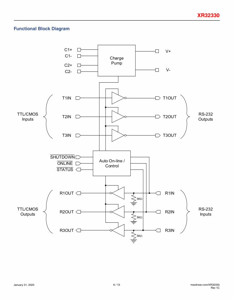
Functional Block Diagram
T1OUT
T2OUTT2IN
T1IN
R1IN
R2IN
R1OUT
R2OUT
SHUTDOWN
ONLINE
STATUS
Charge Pump
C1+
C1-
C2+
C2-
V+
V-
RS-232 Outputs
RS-232 Inputs
TTL/CMOS Inputs
TTL/CMOS Outputs
Auto On-line / Control
5K
5K
T3OUTT3IN
R3INR3OUT5K
January 31, 2020
XR32330
7 / 13 maxlinear.com/XR32330Rev 1C
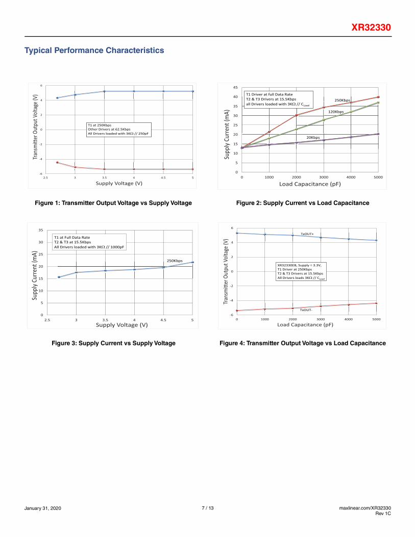
Typical Performance Characteristics
Figure 1: Transmitter Output Voltage vs Supply Voltage Figure 2: Supply Current vs Load Capacitance
-6
-4
-2
0
2
4
6
2.5 3 3.5 4 4.5 5
Trans
mitt
er O
utpu
t Volt
age (
V)
Supply Voltage (V)
T1 at 250KbpsOther Drivers at 62.5KbpsAll Drivers loaded with 3K // 250pF
0
5
10
15
20
25
30
35
40
45
0 1000 2000 3000 4000 5000
Supp
ly Cu
rrent
(mA)
Load Capacitance (pF)
250Kbps
120Kbps
20Kbps
T1 Driver at full Data RateT2 & T3 Drivers at 15.5Kbpsall Drivers loaded with 3K // CLoad
Figure 3: Supply Current vs Supply Voltage Figure 4: Transmitter Output Voltage vs Load Capacitance
0
5
10
15
20
25
30
35
2.5 3 3.5 4 4.5 5
Supp
ly Cu
rrent
(mA)
Supply Voltage (V)
250Kbps
T1 at Full Data RateT2 & T3 at 15.5KbpsAll Drivers loaded with 3K // 1000pF
-6
-4
-2
0
2
4
6
0 1000 2000 3000 4000 5000
Trans
mitt
er O
utpu
t Volt
age (
V)
Load Capacitance (pF)
TxOUT+
TxOUT-
XR32330EB, Supply = 3.3V, T1 Driver at 250Kbps T2 & T3 Drivers at 15.5KbpsAll Drivers loads 3K // CLoad

January 31, 2020
XR32330
8 / 13 maxlinear.com/XR32330Rev 1C
Application Information
General Description
The XR32330 transceiver meets the EIA/TIA-232 and ITU-T V.28/V.24 communication protocols and can be imple-mented in portable or hand-held applications such as barcode scanners as well as point-of-sales terminals, securityand industrial control applications. The XR32330 devicefeatures Exar's proprietary and patented (U.S. 5,306,954)on-board charge pump circuitry that generates ±5.5V RS-232 voltage levels from a single +3.0V to +5.5V power sup-ply.
The XR32330 is a 3-driver/3-receiver device, ideal for por-table or hand-held applications.
The XR32330 is an ideal choice for power sensitivedesigns. The XR32330 devices feature AUTO ON-LINE®circuitry which reduces the power supply drain to a 1µAsupply current.
In many portable or hand-held applications, an RS-232cable can be disconnected or a connected peripheral canbe turned off. Under these conditions, the internal chargepump and the drivers will be shut down. Otherwise, the sys-tem automatically comes online. This feature allows designengineers to address power saving concerns without majordesign changes.
Theory of Operation
The XR32330 series is made up of four basic circuit blocks:
1. Drivers
2. Receivers
3. The Exar proprietary charge pump, and
4. AUTO ON-LINE® circuitry.
Drivers
The drivers are inverting level transmitters that convert TTLor CMOS logic levels to 5.0V EIA/TIA-232 levels with aninverted sense relative to the input logic levels. Typically,the RS-232 output voltage swing is ±5.5V with no load and±5V minimum fully loaded. The driver outputs are protectedagainst infinite short-circuits to ground without degradationin reliability. These drivers comply with the EIA-TIA-232-Fand all previous RS-232 versions. Unused drivers inputsshould be connected to GND or VL.
The drivers have a minimum data rate of 250kbps fullyloaded.
Receivers
The receivers convert +5.0V EIA/TIA-232 levels to TTL orCMOS logic output levels. Receivers are High-Z when theAUTO ON-LINE® circuitry is enabled and activated or whenin shutdown. The truth table logic of the XR32330 driverand receiver outputs can be found in Table 2 on page 11.
Since receiver input is usually from a transmission linewhere long cable lengths and system interference candegrade the signal, the inputs have a typical hysteresismargin of 300mV. This ensures that the receiver is virtuallyimmune to noisy transmission lines. Should an input be leftunconnected, an internal 5KΩ pull-down resistor to groundwill commit the output of the receiver to a HIGH state.
Charge Pump
The charge pump is a Exar–patented design (U.S.5,306,954) and uses a unique approach compared to olderless–efficient designs. The charge pump still requires fourexternal capacitors, but uses a four–phase voltage shiftingtechnique to attain symmetrical ±5.5V power supplies. Theinternal power supply consists of a regulated dual chargepump that provides output voltages of ±5.5V regardless ofthe input voltage (VCC) over the +3.0V to +5.5V range. Thisis important to maintain compliant RS-232 levels regardlessof power supply fluctuations.
The charge pump operates in a discontinuous mode usingan internal oscillator. If the output voltages are less than amagnitude of ±5.5V, the charge pump is enabled. If the out-put voltages exceed a magnitude of ±5.5V, the chargepump is disabled. This oscillator controls the four phases ofthe voltage shifting. A description of each phase follows.
Phase 1
V- charge storage, see Figure 5 — During this phase of theclock cycle, the positive side of capacitors C1 and C2 areinitially charged to VCC. C1+ is then switched to GND andthe charge in C1– is transferred to C2–. Since C2+ is con-nected to VCC, the voltage potential across capacitor C2 isnow 2 times VCC.
Figure 5: Charge Pump - Phase 1
C1 C2
C4
C3
VCC
V+ Storage Capacitor
V- Storage Capacitor
+VCC
-VCC-VCC

January 31, 2020
XR32330
9 / 13 maxlinear.com/XR32330Rev 1C
Phase 2
V- transfer, see Figure 6 — Phase two of the clock con-nects the negative terminal of C2 to the V- storage capaci-tor and the positive terminal of C2 to GND. This transfers anegative generated voltage to C3. This generated voltage isregulated to a minimum voltage of -5.5V. Simultaneous withthe transfer of the voltage to C3, the positive side of capac-itor C1 is switched to VCC and the negative side is con-nected to GND.
Figure 6: Charge Pump - Phase 2
Phase 3
V+ charge storage, see Figure 7 — The third phase of theclock is identical to the first phase — the charge transferredin C1 produces –VCC in the negative terminal of C1, whichis applied to the negative side of capacitor C2. Since C2+ isat VCC, the voltage potential across C2 is 2 times VCC.
Figure 7: Charge Pump - Phase 3
Phase 4
V+ transfer, see Figure 8 — The fourth phase of the clockconnects the negative terminal of C2 to GND, and transfersthis positive generated voltage across C2 to C4, the V+storage capacitor. This voltage is regulated to +5.5V. At thisvoltage, the internal oscillator is disabled. Simultaneouswith the transfer of the voltage to C4, the positive side ofcapacitor C1 is switched to VCC and the negative side is
connected to GND, allowing the charge pump cycle to beginagain. The charge pump cycle will continue as long as theoperational conditions for the internal oscillator are present.
Figure 8: Charge Pump - Phase 4
Since both V+ and V– are separately generated from VCC,in a no–load condition V+ and V– will be symmetrical. Oldercharge pump approaches that generate V– from V+ willshow a decrease in the magnitude of V– compared to V+due to the inherent inefficiencies in the design. The clockrate for the charge pump typically operates at greater than250kHz. The external capacitors can be as low as 0.1µFwith a 16V breakdown voltage rating.
The Exar-patented charge pumps are designed to operatereliably with a range of low cost capacitors. Either polarizedor non polarized capacitors may be used. If polarizedcapacitors are used they should be oriented as shown inthe Typical Applications Circuit. The V+ capacitor may beconnected to either ground or VCC (polarity reversed.)
The charge pump operates with 0.1µF capacitors for 3.3Voperation. For other supply voltages, see the table forrequired capacitor values. Do not use values smaller thanthose listed. Increasing the capacitor values (e.g., by dou-bling in value) reduces ripple on the transmitter outputs andmay slightly reduce power consumption. C2, C3, and C4can be increased without changing C1’s value.
C1 C2
C4
C3
VCC
-5.5V
V+ Storage Capacitor
V- Storage Capacitor
C1 C2
C4
C3
VCC
V+ Storage Capacitor
V- Storage Capacitor
+VCC
-VCC-VCC
C1 C2
C4
C3
VCC
+5.5V
V+ Storage Capacitor
V- Storage Capacitor
January 31, 2020
XR32330
10 / 13 maxlinear.com/XR32330Rev 1C
For best charge pump efficiency locate the charge pumpand bypass capacitors as close as possible to the IC. Sur-face mount capacitors are best for this purpose. Usingcapacitors with lower equivalent series resistance (ESR)and self-inductance, along with minimizing parasitic PCBtrace inductance will optimize charge pump operation.Designers are also advised to consider that capacitor val-ues may shift over time and operating temperature.
AUTO ON-LINE® Circuitry
The XR32330 devices have a patent pending AUTO ON-LINE® circuitry on board that saves power in applicationssuch as hand held and portable systems.
The XR32330 devices incorporate an AUTO ON-LINE® cir-cuit that automatically enables itself when the externaltransmitters are enabled and the cable is connected. Con-versely, the AUTO ON-LINE® circuit also disables most ofthe internal circuitry when the device is not being used andgoes into a standby mode where the device typically draws1µA. This function is externally controlled by the ONLINEpin. When this pin is tied to a logic LOW, the AUTO ON-LINE® function is active. Once active, the device is enableduntil there is no activity on the receiver inputs. The receiverinput typically sees at least +3V, which are generated fromthe transmitters at the other end of the cable with a +5Vminimum.
When the external transmitters are disabled or the cable isdisconnected (see Figure 9), the receiver inputs will bepulled down by their internal 5kΩ resistors to ground. Whenthis occurs over a period of time, the internal transmitterswill be disabled and the device goes into a shutdown orstandby mode. When ONLINE is HIGH, the AUTO ON-LINE® mode is disabled.
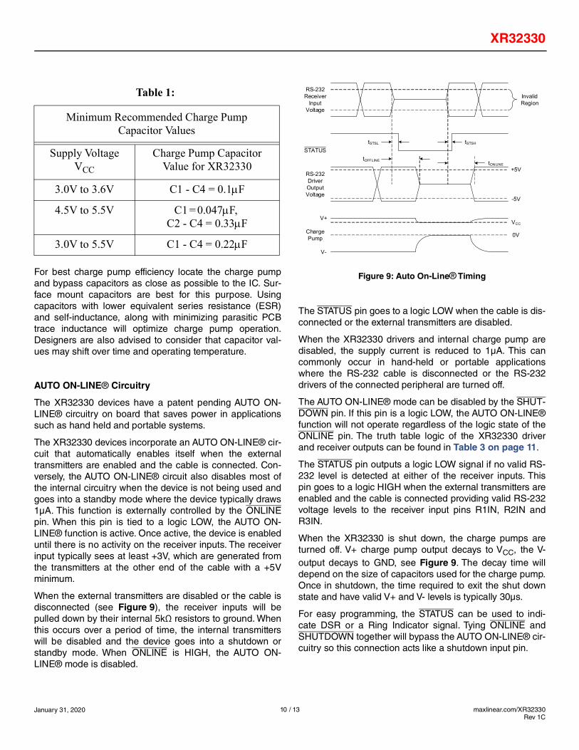
Figure 9: Auto On-Line® Timing
The STATUS pin goes to a logic LOW when the cable is dis-connected or the external transmitters are disabled.
When the XR32330 drivers and internal charge pump aredisabled, the supply current is reduced to 1µA. This cancommonly occur in hand-held or portable applicationswhere the RS-232 cable is disconnected or the RS-232drivers of the connected peripheral are turned off.
The AUTO ON-LINE® mode can be disabled by the SHUT-DOWN pin. If this pin is a logic LOW, the AUTO ON-LINE®function will not operate regardless of the logic state of theONLINE pin. The truth table logic of the XR32330 driverand receiver outputs can be found in Table 3 on page 11.
The STATUS pin outputs a logic LOW signal if no valid RS-232 level is detected at either of the receiver inputs. Thispin goes to a logic HIGH when the external transmitters areenabled and the cable is connected providing valid RS-232voltage levels to the receiver input pins R1IN, R2IN andR3IN.
When the XR32330 is shut down, the charge pumps areturned off. V+ charge pump output decays to VCC, the V-output decays to GND, see Figure 9. The decay time willdepend on the size of capacitors used for the charge pump.Once in shutdown, the time required to exit the shut downstate and have valid V+ and V- levels is typically 30µs.
For easy programming, the STATUS can be used to indi-cate DSR or a Ring Indicator signal. Tying ONLINE andSHUTDOWN together will bypass the AUTO ON-LINE® cir-cuitry so this connection acts like a shutdown input pin.
Table 1:
Minimum Recommended Charge Pump Capacitor Values
Supply Voltage VCC
Charge Pump Capacitor Value for XR32330
3.0V to 3.6V C1 - C4 = 0.1F
4.5V to 5.5V C1 = 0.047F, C2 - C4 = 0.33F
3.0V to 5.5V C1 - C4 = 0.22F
Invalid Region
RS-232 Receiver
Input Voltage
tSTSL tSTSH
tOFFLINEtONLINE
RS-232 Driver Output Voltage
STATUS
+5V
-5V
Charge Pump
V+
V-
VCC
0V

January 31, 2020
XR32330
11 / 13 maxlinear.com/XR32330Rev 1C
Table 2: XR32330 Operation Truth Table
Valid RS-232 Level at Receiver
Input
SHUTDOWN ONLINE TxOUT RxOUT STATUS Mode of Operation
Yes L X High-Z High-Z H Manually forced shutdown
No L X High-Z High-Z L Manually forced shutdown
Yes H L Active Active H Normal Operation (Auto On-Line® enabled)
No H L High-Z Active L Standby Operation due to Auto On-Line® circuitry
Yes H H Active Active H Normal Operation
No H H Active Active L Normal Operation
Table 3: XR32330 Driver and Receiver Truth Table
SHUTDOWN RxIN RxOUT TxIN TxOUT
L X High-Z X High-Z
H L H L H
H H L H L

January 31, 2020
XR32330
12 / 13 maxlinear.com/XR32330Rev 1C
Mechanical Dimensions
24-Pin QFN (4x4mm)

January 31, 2020
XR32330
13 / 13 maxlinear.com/XR32330Rev 1C
MaxLinear, Inc.5966 La Place Court, Suite 100Carlsbad, CA 92008760.692.0711 p.760.444.8598 f.www.maxlinear.com
The content of this document is furnished for informational use only, is subject to change without notice, and should not be construed as a commitment by MaxLinear, Inc. MaxLinear, Inc. assumes no responsibility or liability for any errors or inaccuracies that may appear in the informational content contained in this guide. Complying with all applicable copyright laws is the responsibility of the user. Without limiting the rights under copyright, no part of this docu-ment may be reproduced into, stored in, or introduced into a retrieval system, or transmitted in any form or by any means (electronic, mechanical, photo-copying, recording, or otherwise), or for any purpose, without the express written permission of MaxLinear, Inc.
Maxlinear, Inc. does not recommend the use of any of its products in life support applications where the failure or malfunction of the product can reason-ably be expected to cause failure of the life support system or to significantly affect its safety or effectiveness. Products are not authorized for use in such applications unless MaxLinear, Inc. receives, in writing, assurances to its satisfaction that: (a) the risk of injury or damage has been minimized; (b) the user assumes all such risks; (c) potential liability of MaxLinear, Inc. is adequately protected under the circumstances.
MaxLinear, Inc. may have patents, patent applications, trademarks, copyrights, or other intellectual property rights covering subject matter in this docu-ment. Except as expressly provided in any written license agreement from MaxLinear, Inc., the furnishing of this document does not give you any license to these patents, trademarks, copyrights, or other intellectual property.
MaxLinear, the MaxLinear logo, and any MaxLinear trademarks, MxL, Full-Spectrum Capture, FSC, G.now, AirPHY and the MaxLinear logo are all on the products sold, are all trademarks of MaxLinear, Inc. or one of MaxLinear’s subsidiaries in the U.S.A. and other countries. All rights reserved. Other com-pany trademarks and product names appearing herein are the property of their respective owners.
© 2014 - 2020 MaxLinear, Inc. All rights reserved.
Ordering Information(1)
NOTES:1. Refer to http://www.maxlinear.com/XR32330 for most up-to-date Ordering Information.2. Visit www.maxlinear.com for additional information on Environmental Rating.
Revision History
Part Number Operating Temperature Range Package Packaging Method Lead-Free(2)
XR32330EBERTR-F -40°C to +85°C 24-pin QFN Tape and Reel Yes
Revision Date Description
1A November 2014 Initial release of datasheet. ECN 1446-08 Nov 2014
1B June 2016 Update tape and reel part number.
1C January 2020 Update to MaxLinear logo. Update ordering information.