Embed Size (px)
Citation preview

8/11/2019 2_template Fyp Final Report4
http://slidepdf.com/reader/full/2template-fyp-final-report4 1/75
DECLARATION
It is declared that all the materials in this report are the result of my own work
and all materials which are not the result of my own work have been clearly
acknowledged in this report.
Signed:………………………………….
Date:…………………………………….
ii
8/11/2019 2_template Fyp Final Report4
http://slidepdf.com/reader/full/2template-fyp-final-report4 2/75
ACKNOWLEDGEMENTS
All praises to Allah, unto im belongs all the knowledge and understanding. I would
like to acknowledge and e!tend my heartily gratitude to the following people
without whom the completion of this research would not have been possible. I wish
to e!press my appreciation and thankfulness to my supervisor, Dr. "idad Ismail who
was very helpful and offered invaluable advice, support and guidance# not forgetting
my initial supervisor, Dr. $andeep Singh for his encouragement and advice that
motivated me to take up this research. $y appreciation to my manager, %im &ok
&eong, who shares the same admiration for knowledge and 'technology(# for his
persistent support in all my works. I would also like to convey thanks to Agilent
)echnologies for funding the materials in this research. )o my colleagues %aw *oon
"an, )oh +hee %eng and Ahmad elmi $okhtar for their relentless help and
technical contribution, let me e!press my sincere gratitude. I wish to e!press my
love and gratitude to my beloved wife, Alhan arhanah, my children and family# for
their understanding and sacrifice, throughout the duration of my study. I thank you
to all of you and indeed Allah is the best for reward and the best for the final end.
iii
8/11/2019 2_template Fyp Final Report4
http://slidepdf.com/reader/full/2template-fyp-final-report4 3/75
DESIGN AND DEVELOPMENT OF A 3.6 GHZ DIELECTRIC RESONATOR
OSCILLATOR WITH WIDE TUNING SENSITIVITY
ABSTRACT
An oscillator is re-uired as a second stage % in a superheterodyne SA. )he
oscillator operating fre-uency is a fi!ed /.0 12, which is at the lower end of the
microwave fre-uency range. )here are several options of active devices and
resonators that can be considered for the oscillator. A bipolar 3unction transistor
4*5)6 is chosen for the amplifier block due to its low flicker noise corner fre-uency
and a dielectric resonator 4D76 is chosen for its high 8 factor. )his combination
yields a low phase noise oscillator. Apart from its high 8 factor, a D7 is a high
dielectric constant ceramic thus enabling a miniaturi2ed microwave oscillator design
compared to a cavity resonator. A varactor9tuned techni-ue is adopted because it
results in a simple planar circuit design compared to optically and magnetically tune
D7. )his dielectric resonator oscillator 4D76 must have very high fre-uency
accuracy. )he SA is specified to operate from °+ to ;;°+, thus among the design
re-uirement for the D7 is to be operable in a wide temperature range and, to last
for many, many years. ence the D7 is controlled by a phase9locked loop 4<%%6.
As the D7 signal drifts with temperature as well as due to aging, a wide tuning
range is necessary to guarantee a reliable and repeatable performance over its
operating life.
An e!isting D7 with a tuning range of .=>? at of /.0 12 was used as a
benchmark. )he development of the new D7 began with investigation on several
proposed varactor9tuned D7 resonant structures. )he resonant structures were
observed for the resonant fre-uency tuning range, the linearity of resonant
fre-uencies versus tuning voltages and the tuning sensitivity. )he promising D7
resonant structures @ with wide tuning range, linear response and high tuning
sensitivity, were further analy2ed to understand the resonant structures coupling
mechanism as well as the potential effect on the D7 performance like phase noise.
)he successful D7 resonant structure combined with the *5) amplifier circuit
formed the D7. )he first D7 is a positive feedback oscillator# however due to the
resonant structure high insertion loss compared with the available amplifier gain, theD7 failed to work. An alternative negative resistance oscillator was then
iv
8/11/2019 2_template Fyp Final Report4
http://slidepdf.com/reader/full/2template-fyp-final-report4 4/75
developed, also using the same model *5). It worked based on signal reflection
between the resonant structure port and the *5) emitter 3unction which posed a
negative real impedance# it proved successful. )he newly developed negative
resistance D7 performance was measured and compared with the benchmark
D7. )he new D7 yields a tuning range of / $2 or .0;? at /.0 12 and a
tuning sensitivity of ./ $2BC. owever, the new D7 phase noise degraded by
about = d* compared with the benchmark D7.
v
8/11/2019 2_template Fyp Final Report4
http://slidepdf.com/reader/full/2template-fyp-final-report4 5/75
TABLE OF CONTENTS
A+&"%ED1E$E)S.......................................................................................iii
A*S)7A+)...............................................................................................................iv
)able of +ontents........................................................................................................vi
%IS) I1F7ES....................................................................................................i!
%IS) )A*%ES......................................................................................................!i
%IS) SG$*%S.................................................................................................!ii
A**7ECIA)IS...................................................................................................!iv
= I)7DF+)I.............................................................................................=;
=.= $otivation @ A igh )uning Sensitivity Second Down9+onverter %ocal
scillator................................................................................................................=;
=. 7esearch <roblem Statement.......................................................................=;
=./ 7esearch b3ectives....................................................................................=0
=.> 7esearch Scope and %imitations.................................................................=H
=.; 7esearch +ontribution.................................................................................=
=.0 )hesis rgani2ation.....................................................................................=
%I)E7A)F7ES 7ECIE"................................................................................
.= $icrowave re-uencies Sources.................................................................
. Active Device +onsideration for scillator................................................=
./ igh 89factor 7esonator............................................................................./
.> Dielectric "aveguide as a $icrowave 7esonator.......................................>
.; Discussion on D7 tuning techni-ues prior works.......................................;
.0 Summary.....................................................................................................0
/ $E)D%1G............................................................................................J
/.= Dielectric 7esonator scillator Specification.............................................J
/. Development lowchart............................................................................../
vi
8/11/2019 2_template Fyp Final Report4
http://slidepdf.com/reader/full/2template-fyp-final-report4 6/75
/./ Dielectric 7esonator..................................................................................../=
/./.= 7esonant $ode..................................................................................../=
/.> 7esonance Structure +onstruction..............................................................//
/.>.= $etal Enclosure Effect on 7esonant $ode and re-uency................./>
/.>. D7 +oupling to $icrostrip................................................................../H
/.>./ $echanical Ad3ustment of 7esonant re-uency................................./J
/.>.> Electronic )uning Element @ Caractor.................................................>
/.>.; $icrostrip Stub +oupled Caractor )uning @ )unable 7esonant +ircuit
>/
/.; Summary.....................................................................................................>0
> 7ESF%)S AD DIS+FSSI........................................................................>H
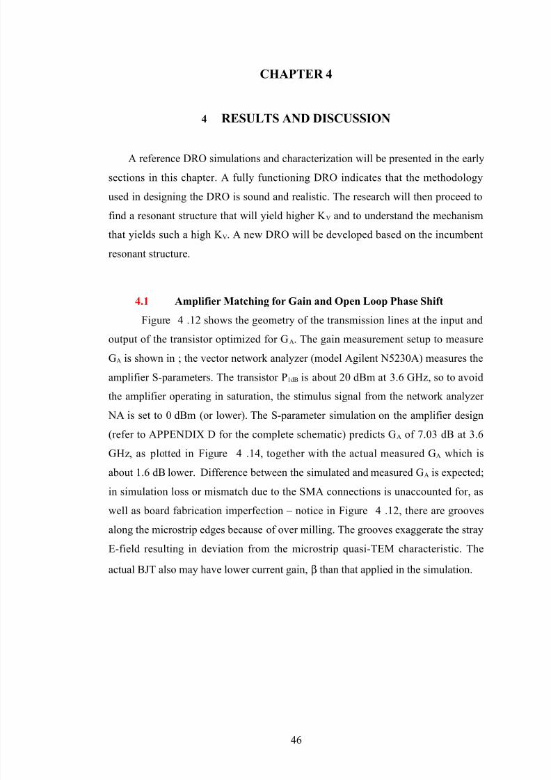
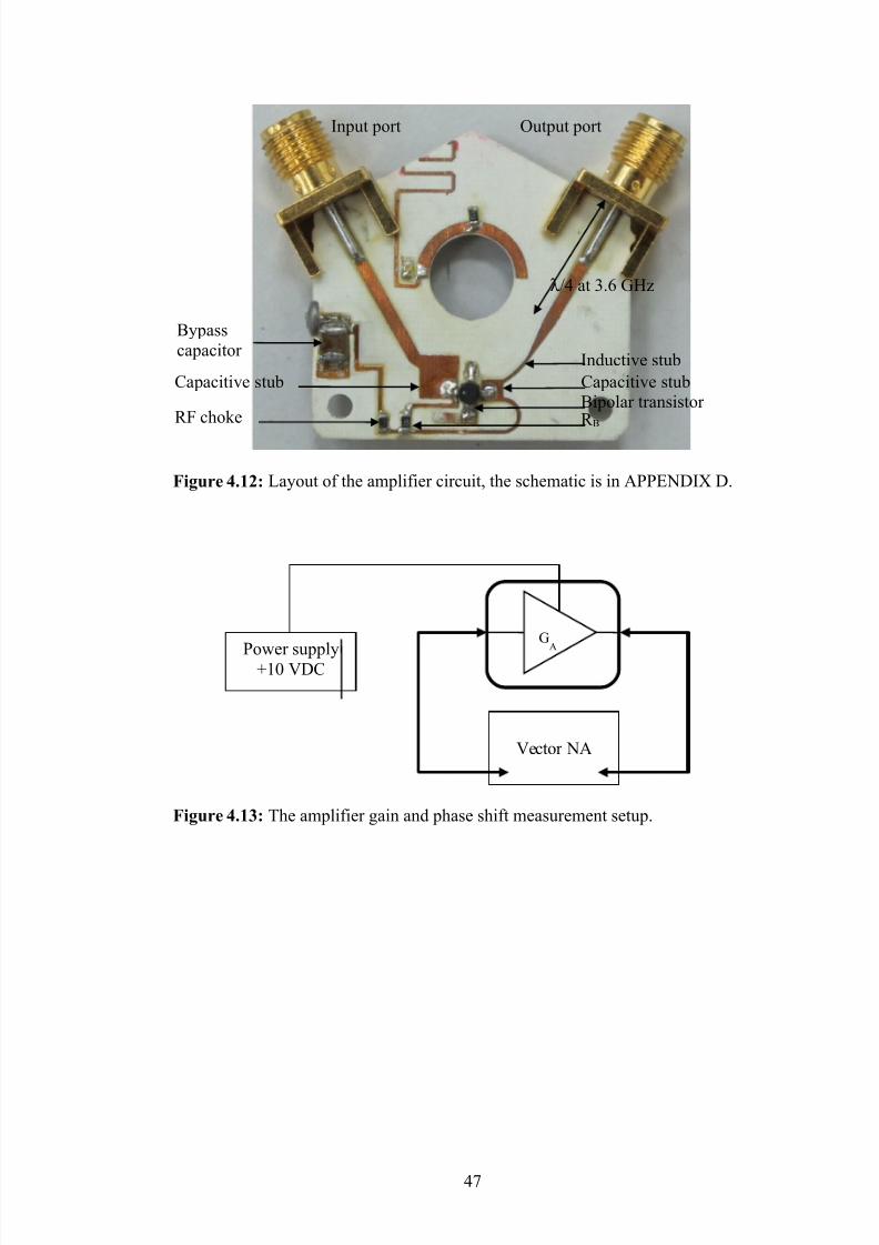
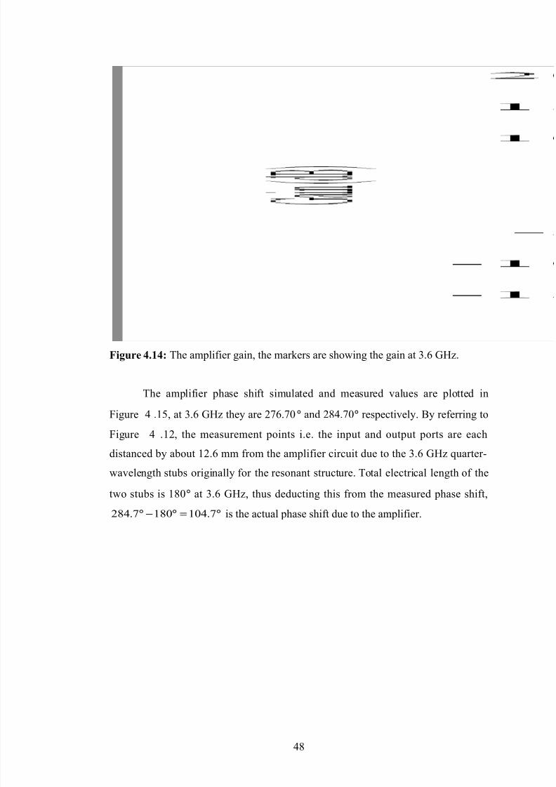
>.= Amplifier $atching for 1ain and pen %oop <hase Shift.........................>H
>.=.= <hase oise..........................................................................................;=
>.=. )unable 7esonance Structure +oupling to Amplifier *lock...............;/
>.=./ Signal +oupling to utput...................................................................;>
>. Initial D7 <erformance............................................................................;0
>..= undamental re-uency and )uning Sensitivity.................................;0
>.. <ower K armonics.............................................................................;
>../ <hase oise..........................................................................................0
>./ Summary.....................................................................................................0=
; ++%FSI AD F)F7E "7&S........................................................0
;.= +onclusion on the igh & C and "ide )uning 7ange D7 Design............0
;. uture "ork on the igh & C D7..............................................................0/
;..= <hase oise Improvement...................................................................0/
;.. urther & C or )uning 7ange Improvement for +ost 7eduction
pportunity........................................................................................................0>
7EE7E+ES..........................................................................................................0;
A<<EDIL A............................................................................................................H
vii

8/11/2019 2_template Fyp Final Report4
http://slidepdf.com/reader/full/2template-fyp-final-report4 7/75
A<<EDIL *............................................................................................................H/
A<<EDIL +............................................................................................................H>
A<<EDIL D............................................................................................................H;
A<<EDIL E............................................................................................................H0
%IS) <F*%I+A)IS.......................................................................................HH
viii
8/11/2019 2_template Fyp Final Report4
http://slidepdf.com/reader/full/2template-fyp-final-report4 8/75
LIST OF FIGURES
Page
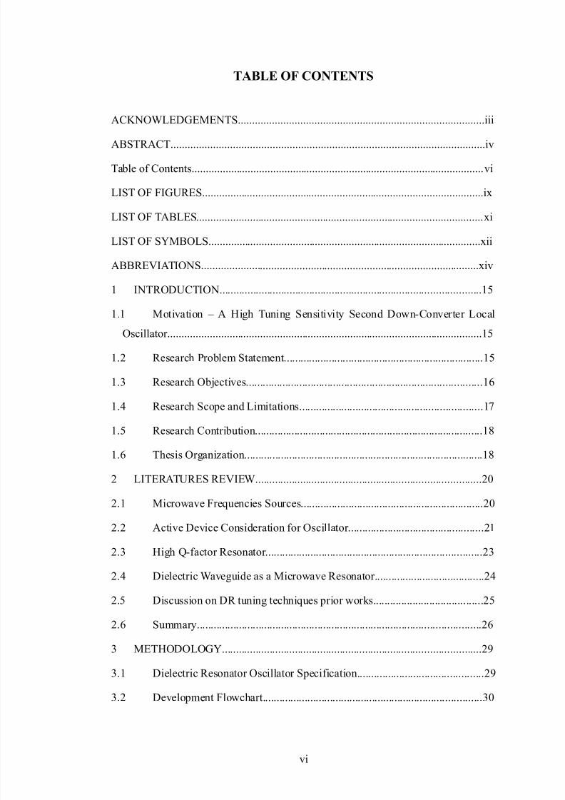
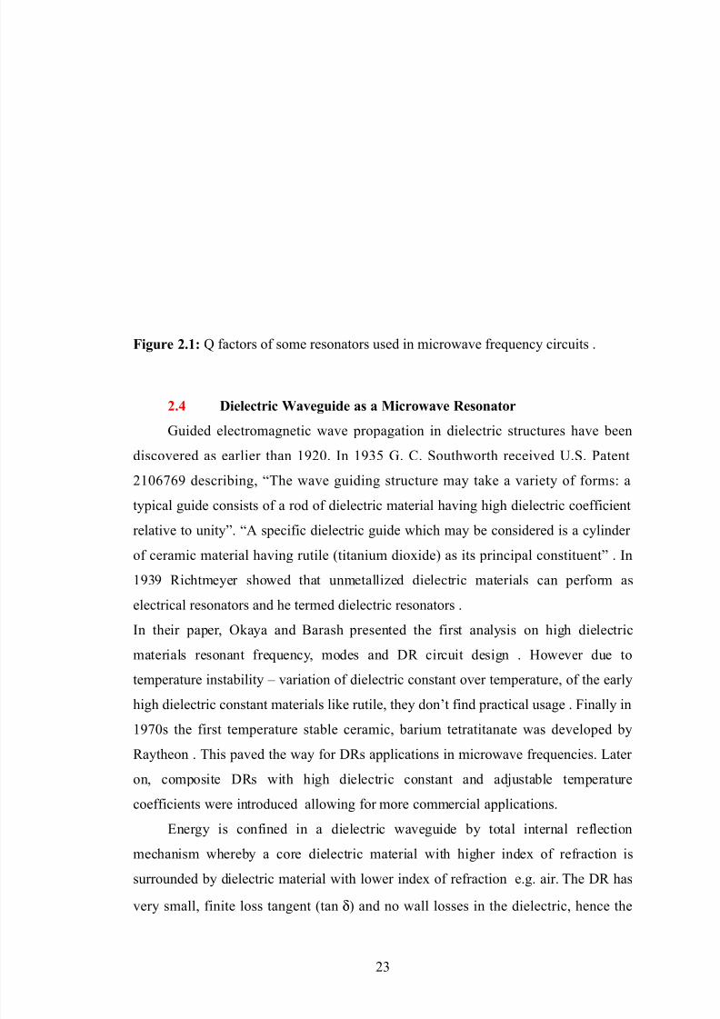
igure .=: 8 factors of some resonators used in microwave fre-uency circuits
M0, , J, //9/0N.............................................................................................>
igure /.=: A cylindrical D7 with )E=O mode, 4b6 top view and 4c6 side view, in the
case where % P D M>/N...................................................................................../
igure /.: 4a6 $icrostrip, )E$ mode M0>N# 4b6 dielectric resonator )E=
resonant
mode coupling to microstrip )E$ mode# QQ =............................................/H
igure /./: Electrical e-uivalent schematic circuit of the dielectric resonator
coupling to a microstrip line............................................................................../
igure /.>: Initial stage breadboard circuit developed to characteri2e microstrip lines
coupling to the dielectric resonator, dotted lines are indicating ma!imum 9
field coupling points........................................................................................../J
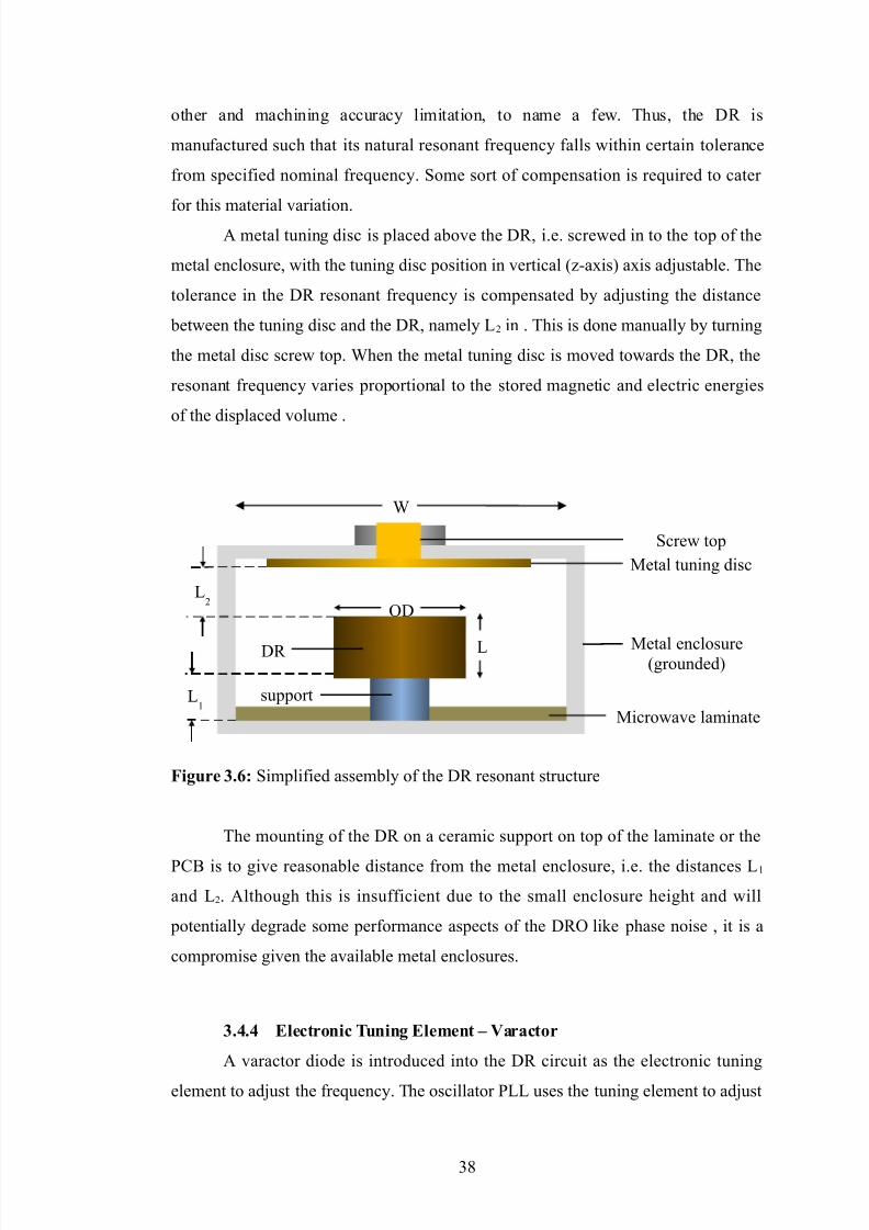
igure /.;: Simplified assembly of the D7 resonant structure..................................>
igure /.0: **;H diode capacitance 4+)6 at = $2 versus the reverse voltage
applied or the vtune, taken from the datasheet M0N..............................................>=
igure /.H: ADS model of packaged **;H constructed from its S<I+E model and
package model...................................................................................................>
igure /.: Simulation of packaged **;H in ADS and E$DS at = $2...............>>
igure /.J: )unable resonant circuit assembly..........................................................>0
igure /.=: <lot of the tunable resonant circuit simulated and measured
transmission response 4S=6................................................................................>H
igure >.=: %ayout of the amplifier circuit, the schematic is in A<<EDIL D........>J
igure >.: )he amplifier gain and phase shift measurement setup.......................... >J
igure >./: )he amplifier gain, the markers are showing the gain at /.0 12..........;
igure >.>: )he amplifier phase shift, the markers are phase shifts at /.0 12........;=
igure >.;: Simulated and measured noise figure of the designed amplifier............;
igure >.0: )he amplifier noise figure measurement setup.......................................;
igure >.H: <redicted phase noise for the designed oscillator....................................;/
igure >.: $easured response of the resonant structure described in section /.>.;.;>
igure >.J: +omplete oscillator circuit resting in bottom enclosure..........................;;
igure >.=: scillator signal coupling to the output................................................;H
i!
8/11/2019 2_template Fyp Final Report4
http://slidepdf.com/reader/full/2template-fyp-final-report4 9/75
igure >.==: Spectrum measurement set up...............................................................;H
igure >.=: D7 center fre-uency reading.............................................................;
igure >.=/: )he positive feedback D7 f versus vtune.............................................;J
igure >.=>: re-uency spectrum of the dielectric resonator oscillator....................0
igure >.=;: <hase noise measurement using Agilent E;;* signal source analy2er
...........................................................................................................................0=
igure >.=0: Dielectric resonator oscillator phase noise, measured and simulated.. .0
!
8/11/2019 2_template Fyp Final Report4
http://slidepdf.com/reader/full/2template-fyp-final-report4 10/75
LIST OF TABLES
Page
)able .=: Summary of prior works that achieved wide tuning bandwidth...............H
)able /.=: Specification of the D7..........................................................................J
)able /.: verview of ceramic materials available for the dielectric resonator....../=
)able /./: ff9the9shelf metal enclosure dimensions................................................/>
)able /.>: +alculated waveguide resonant wavelength,λdB for available materials
M/0N...................................................................................................................../;
)able /.;: Electrical properties of >; series dielectric resonator fabricated for this
design, based on the manufacturer measurement............................................../0
)able /.0: abricated dielectric resonator physical dimensions................................/0
)able >.=: Antenna9waveguide structure simulation and measurement data.............;0
!i
8/11/2019 2_template Fyp Final Report4
http://slidepdf.com/reader/full/2template-fyp-final-report4 11/75
LIST OF SYMBOLS
Γ 7eflection coefficient
λ "avelength in vacuum, free space or air ω re-uency in radian
β )ransistor current gain
ω+ 7esonant fre-uency in radian
λd 1uide wavelength
εr Dielectric constant
=B f licker noise
+res Dielectric resonator e-uivalent capacitance
+) Caractor capacitance
oise figure
Φ Caractor built9in potential∆ f Instantaneous oscillation fre-uency
f + 7esonant fre-uency
f m *aseband fre-uency, offset fre-uency
f fundamental signal or carrier fre-uency
f ) )ransit fre-uency
1A Amplifier power gain
1a 1allium nitride
I+ +ollector D+ current
k *olt2mann constant, =./0;/ R =9/ 5& 9=
&a 7efering to = @ H 12 fre-uency band
& C oscillator tuning sensitivity or oscillator gain%res Dielectric resonator e-uivalent inductance
%) )uning stub e-uivalent inductance
+oupling coefficient 4i.e. in transformer6
<=d* utput power = d* compression point
< utput power
8% %oaded 8
8F Fnloaded 8
) )emperature 4in &elvin6
tan δ %osses in the 4dielectric6 material
)E=δ)ransverse electric resonant mode in dielectric resonator
)E== )ransverse electric resonant mode in cavity resonator
)E=== )ransverse electric resonant mode in cavity resonator
v b *ase voltage
C++ Supply voltage, e.g. at collector
Ci Input signal, in volt
Co utput signal, in volt
vtune Caractor bias, tuning voltage
vD+ Instantaneous varactor tuning voltage
"φ Single sided noise spectral density
!ii
8/11/2019 2_template Fyp Final Report4
http://slidepdf.com/reader/full/2template-fyp-final-report4 12/75
ABBREVIATIONS
ADS Advanced Design System
*5) *ipolar 3unction transistor +" +ontinuous wave
D+ Direct current
D7 Dielectric resonator
D7 dielectric resonator oscillator
E9field Electric field
E$DS Electro$agnetic Design System
E) ield effect transistor
9field $agnetic field
I% Insertion loss
% %ocal oscillator
<+* <rinted circuit board<%% <hase9locked loop
SA Spectrum analy2er
SSA Signal source analy2er
)E$ )ransverse electric magnetic propagation mode
)") )ravelling wave tube
F Fltra high fre-uency
C+ Coltage controlled oscillator
GI1 Gttrium9iron9garnet
!iii
8/11/2019 2_template Fyp Final Report4
http://slidepdf.com/reader/full/2template-fyp-final-report4 13/75
CHAPTER 1
1 INTRODUCTION
)here are many microwave fre-uency oscillators in the market serving the ever
growing electronic communications. $ost of the shelf devices are tailored to the
commercial applications like mobile phones, wireless broadband data and
broadcasting industries. Although there are suppliers that do custom designs for
uni-ue applications or low volume market, they come with high price tags# hence the
need for in9house designs. Secondly, proprietary technologies are best kept with in9house design.
1.1 M!"#a!"$ % A H"g& T'$"$g Se$("!"#"!) Se*$+ D,$-C$#e!e
L*a/ O(*"//a!
A swept signal spectrum analy2er 4SA6 re-uires a fi! fre-uency oscillator
operating at /.0 12 for its second down9converter block. Although there is probably
an application out there that works at /.0 12, a tight re-uirement on this oscillator,
as the SA is a test and measurement instrument, means the available of9the9shelf
oscillator may not meet the re-uirement @ electrical and mechanical specifications as
well as physical si2e 4form, fit and function6. )he SA is specified to operate over a
wide temperature range i.e. from °+ to ;;°+ and over a long period of time. )hus the
oscillator fre-uency may drift over temperature as well as over time. )herefore, the
oscillator re-uires a tuning mechanism for the fre-uency drift compensation# the
fre-uency correction will be controlled by a <%%.
1.0 Re(ea*& P/e2 S!a!e2e$!
In microwave fi!ed fre-uency oscillators as well as microwave filters, some
limited tuning capability is necessary for center fre-uency ad3ustment. Dielectric
resonator materials have some fabrication tolerance which results in resonant
fre-uency variation. )his problem is commonly addressed by means of mechanical
ad3ustments. owever this is a onetime ad3ustment during manufacturing and it
=>
8/11/2019 2_template Fyp Final Report4
http://slidepdf.com/reader/full/2template-fyp-final-report4 14/75
cannot correct the resonant fre-uency should there be drifts throughout the device
operating life. A broad fre-uency range electronically tuned method as proposed in
this research offers a solution to alleviate this problem. It should be applicable either
in dielectric resonator oscillators and filters.
As for filters, particularly band pass filters, apart from the problem discussed
above, having an electronic tuning capability allows for bands selection. I.e. instead of
designing a broad band filter that covers the whole fre-uency channels, a narrower
band pass filter could be designed which may improves ad3acent channel re3ection.
)he filter can be controlled to 'pass( only the channels it is operating.
)he subse-uent problem which will be the focus of this research is an e!ample where
a broad, electronically tuned capability is re-uired. )he SA second local oscillator
specification re-uires a tuning bandwidth of = $2 and tuning sensitivity, & C =
$2BC6 to enable the oscillator to provide a reliable and consistent fi!ed /.0 12
signal to the down converter mi!er in the SA. )he output power for the /.0 12
signal is T/ d*m ± = d*. <hysically, the oscillator must be small enough to fit in a
typical bench top SA.
%ooking at the fre-uency and output power re-uirement as well as the si2e, a
solid state oscillator is the most sensible option. "ith the choice of resonators
available a planar circuit is feasible. or a low phase noise oscillator design# the solid
state active device choice, e.g. a transistor or a diode must consider the flicker noise#
and secondly a high 89factor resonator . )he temperature coefficient of the resonator
resonance fre-uency must have a low part per million 4p.p.m.6 number for stability
over wide temperature range. $aterials selection will be further discussed in the
following sections.
1.3 Re(ea*& Oe*!"#e(
*ased on the defined problem statement, the ob3ectives of the research can be
defined as follows:
4i6 )o design a dielectric resonator oscillator 4D76 that must achieve a tuning
bandwidth of at least = $2 with tuning voltage of C to T= C.
)he main ob3ective of this design is to establish a circuit techni-ue that can achieve
the wide tuning bandwidth# the choice of materials like transistor, resonator and
=;
8/11/2019 2_template Fyp Final Report4
http://slidepdf.com/reader/full/2template-fyp-final-report4 15/75
varactor are secondary. In this study, a method for achieving wide tuning bandwidth
and high tuning sensitivity, & C for D7 will be investigated and verified with a final
design of the D7.
4ii6 )o fabricate and measure the proposed D7 design that considers the need for
it to suit manufacturing re-uirement.
)he solution is using low cost, off9the9shelf components# manufacturable with
e!isting industrial technology e.g. printed circuit board 4<+*6 in mass production
environment.
4iii6 )o analy2e and validate the performance of the proposed D7 for practical
oscillator application and finali2ed the specification of such D7 in which, the tuning
sensitivity must be linear to ease <%% control.
)his study only focuses on the design of the wide tuning bandwidth D7.
1.4 Re(ea*& S*5e a$+ L"2"!a!"$(
)he scope of this study is to find an electronically9tuned techni-ue# that yields a
wide tuning bandwidth for a passive dielectric resonator 4D76 circuit and
subse-uently apply it to a D7 design and test the D7 functionality. )he activities
include:
=. %iteratures review on microwave signal sources, D7 technologies, related
materials and devices to construct microwave oscillators and prior works and
techni-ues on D7s#
. +haracteri2e a D7 circuit and the corresponding D7 4previously developed
by the author6 to be used as a reference for the prospective oscillator,
/. Simulation of several initial proposed passive D7 circuits, fabrication of the
designed circuits and measurements of the circuits.
>. <romising circuits will be further analy2ed to find a trend that will give a wide
tuning bandwidth. inally the passive circuits will be adopted into D7 designs to
prove the techni-ue effectiveness.
)his research does not intend to include in9depth study and improvement on
phase noise for the prospective D7# however phase noise performance of the
'reference( and 'prospective( oscillators will be measured for completeness.
=0
8/11/2019 2_template Fyp Final Report4
http://slidepdf.com/reader/full/2template-fyp-final-report4 16/75
In the design, especially in simulation related to non9linearity parameters like the
amplifier gain and its open loop phase# reflection coefficient of negative resistance
port are not very correlated to their corresponding measurements. )his is due to
limitation to components non9linearity parameters in the models in particular the
transistor.
+ircuit fabrication accuracy is as good as the prototyping machine capability,
hence some losses in measurements that are unaccounted for in simulations like
insertion loss and amplifier gain. )he three dimensional electromagnetic field
simulator, E$DS, uses a lot of computer resources. Additional components used in
supporting measurement like 7 S$A connectors are not included in the three
dimensional electromagnetic field simulation to reduce model comple!ity.
1. Re(ea*& C$!"'!"$
)his research proposes a techni-ue to increase D7 tuning range with high
tuning sensitivity# suitable where only small vtune range is available. )he techni-ue
offers a low impedance varactor tuning stub that couples to the D7, e!ploiting the D7
)E=δ resonant mode. It is a practical approach where mass production is intended as
most of the components to build the circuit, are available off the shelf. $inimal
custom9made components are necessary, which are uni-ue to the desired operating
fre-uency such as the metal enclosure, the D7 and the <+*, of course. )he techni-ue
is also applicable for D7 filter application as stated earlier in Section =..
1.6 T&e("( Oga$"7a!"$
)his introductory chapter presents the background of the problem that leads to
this research and development on the prospective D7. )his is followed by
ob3ectives of the study and the e!pected end results.
)he following literature review chapter begins with a brief review of microwave
sources technologies currently available, related materials and devices to construct
microwave oscillators and how the selection of materials relates to the theory, some
fundamentals on D7 applications followed by discussion on D7s prior works and
techni-ues.
=H
8/11/2019 2_template Fyp Final Report4
http://slidepdf.com/reader/full/2template-fyp-final-report4 17/75
In chapter /, the research flowchart is presented. rom here the proposed
passive tunable resonant circuits and e!periments will be laid out to find out a tunable
circuit that is promising for a wide tuning bandwidth. inally a brief notes on
oscillator fundamentals.
In +hapter > the analysis and results from all e!periments are presented and
analy2ed in determining a tunable circuit that can yield a wide tuning bandwidth. )he
second part of this chapter elaborates how a potentially wide tuning bandwidth
resonant circuit is designed into a D7. )he potential wide tuning bandwidth D7
design presented in +hapter > is further discussed in +hapter ;, in comparison with
e!isting and prior works or reports.
inally the study(s findings is discussed and summed up# and in particular in
the 3ustification of adopting the design in the said application as well as other
potential applications. <otential future works would also be discussed in which how to
possibly improves the phase noise, an important figure of merit for an oscillator and
secondly the possibilities to further increase the tuning range andBor tuning sensitivity,
& C.
=
8/11/2019 2_template Fyp Final Report4
http://slidepdf.com/reader/full/2template-fyp-final-report4 18/75
CHAPTER 0
0 LITERATURES REVIEW
In general, microwave fre-uency signal sources are either wide band and tunable
like GI19tuned oscillators, voltage controlled oscillators and fre-uency multipliers# or
fi!ed fre-uency like coa!ial resonator oscillators and D7s. Although categori2ed as
fi!ed fre-uency, coa!ials and D7s do have limited tunability for fre-uency
correction. )he categories only imply the oscillators( applications. A microwave
oscillator 4wide band or fi!ed fre-uency6 is basically a high 89factor resonator with
an appropriate coupling structure, couples to an active device.
0.1 M"*,a#e Fe8'e$*"e( S'*e(
$icrowave fre-uencies range from / $2 to / 12, i.e. e-uivalent to
wavelength of one meter down to one millimeter respectively . )his is a broad
definition that includes ultra high fre-uencies 4F6 all the way to millimeter waves.
+ommonly, microwave fre-uencies usually refer to / 12 to / 12, or = cm to =
cm wavelength at minimum, however in 7 engineering the lower boundary is
usually at = 12 4/ cm6, and the upper around = 12 4/ mm6.
$icrowave sources have different types of constructions and unlike lower
fre-uencies, are not limited to <+*. Cacuum tube devices include the magnetron,
klystron, traveling9wave tube 4)")6, and gyrotron, and operate on the ballistic
motion of electrons in a vacuum under the influence of controlling electric or
magnetic fields. Cacuum tube devices are cumbersome but are capable of very high
output power, for e!ample a continuous wave 4+"6 heli! )") yields an output
power in the range of several kilowatts at L band . A 'microwave amplification by
stimulated emission of radiation( 4maser6 produces coherent electromagnetic waves
through amplification due to stimulated emission# it has a very high fre-uency
precision . Solid9state sources can be constructed from bipolar 3unction transistors
4*5)6, field9effect transistor 4E)6 @ at high microwave fre-uencies, tunnel diodes,
1unn diodes, and I$<A)) diodes. Solid state microwave oscillators are relatively
smaller in si2e than the above two sources# and can be either planar circuits i.e. on
=J
8/11/2019 2_template Fyp Final Report4
http://slidepdf.com/reader/full/2template-fyp-final-report4 19/75
<+*s or combination of planar circuits and physical structures, depending on the
choice of resonators. Fntil recently, solid state devices are capable of low to medium
power handling in microwave applications. "ith the advent of 1a devices,
wideband capability and high power applications are possible all way into &a band .
Such prospect combined with lower cost gives microwave solid state oscillators a
promising future.
0.0 A*!"#e De#"*e C$("+ea!"$ 9 O(*"//a!
An important parameter for any oscillators is its signal purity. As for harmonics,
if any of the harmonics signal is too high, it could cause the <%% to lock on that
harmonic instead of the fundamental signal, f # secondly it could also create a spurious
signal at a mi!er output like the one this oscillator is intended for. A low pass filter
can be added at the output of the oscillator to suppress the harmonics. )he harmonics
arise due to the active device non9linearity. )o reduce the harmonics power level, the
device must have much higher <=d* than the re-uired output power for the f .
or phase noise, the active device must have low =B f noise 4or the flicker noise6
because this noise is up converted to the sideband of the oscillator output signals. *5)
has large parasitic capacitance to the ground, resulting in reduction of the =B f noise.
Also, =B f noise is directly proportional to the current density in the transistor. %argetransistors with high ma!imum collector current, when used at low currents will give
the best =B f performance. armonics can mi! =B f noise up and mi! back to the
fundamental signal @ this would cause higher phase noise. +hoosing *5) with low f ),
means less harmonics generated and thus lower phase noise. A simple guideline is the
device f ) should be two or three times the operating fre-uency . E) devices although
they too can offer high <=d*, unfortunately have higher =B f corner fre-uency. A typical
submicron $SE) device, with a bias current of several hundred microamperes
would show a =B f corner fre-uency around = $2# and this is worse than *5) . E)
would be considered for oscillators operating beyond = 12 if the phase noise is not
demanding as there aren(t many *5)s available for operation above = 12. ow
with the presence of hetero3unction bipolar transistors 4*)6, the bipolar transistor
technology is making its way even beyond 12 as demonstrated by # the *)
phase noise performance is either better or comparable to *5).
1unn diodes are applied mostly in higher microwave fre-uencies i.e. = 12 onwards
because the 1unn diode oscillators re-uire cavity resonators, many works discussed
8/11/2019 2_template Fyp Final Report4
http://slidepdf.com/reader/full/2template-fyp-final-report4 20/75
oscillator applications in millimeter waves for e!ample , and an oscillator at /; 12
presented by has -uite low phase noise too e.g. 9=/ d*cB2 to 9=; d*cB2 at =9
k2 offset from f . )hough theoretically it is possible to use the 1unn diode in this
work, the cavity resonator si2e at /.0 12 makes it impractical for miniaturi2ation.
)he cavity resonator will be further e!plained in the following section. Fntil recently,
for many 1unn diode oscillators, the fre-uency tuning is reali2ed by the 1unn diode
D+ bias ad3ustment to create fre-uency pushing, this will complicates the design .
owadays though, there are varactors offered for 1unn diode oscillator applications,
like those offered by ev )echnologies . I$<A)) diodes are similar to 1unn diodes
though they are not interchangeable. )heir D+ operating current is typically in
hundreds of milliamps with output power ranges from tens to hundreds of miliwatts.
)here are microwave voltage controlled oscillator 4C+6 designs on
integrated circuit 4I+6 for tunable oscillator applications with tuning range in
hundreds of $egahert2 to a few 1igahert2. <hase noise of tunable oscillator will
suffer degradation due to the presence of a tuning element like varactor# and the wider
the tuning bandwidth the poorer the phase noise . *ulk acoustic wave 4*A"6
resonator oscillator is also an I+ based but it is for a fi!ed fre-uency or narrow band
application. or technological reasons *A"9based oscillators are limited up to 12
though there are works showing *A"9based oscillators at higher fre-uencies,
achieved by some sort of fre-uency multiplication. or a uni-ue application i.e. this
/.0 12 oscillator, an integrated circuit C+ would re-uire a substantial financial
investment.
f all the choices of solid state devices mentioned above, discreet *5) is the
most suitable for low noise design especially for low microwave fre-uencies# in fact
7egis et al stated clearly their choice of *5) in for their ultra low phase noise
oscillator# and "arburton for his / 12 oscillator .+onsidering cost, an off the shelf
component is preferred over a dedicated I+ designed oscillator.
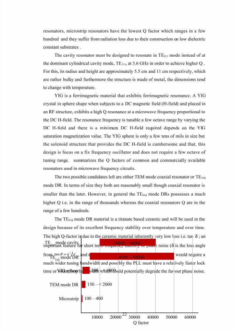
0.3 H"g& :-9a*! Re($a!
)here are many choices of microwave resonators available for application in the
S9band. Among others are cavity resonator , yttrium9iron9garnet 4GI16 crystal ,
dielectric resonators @ both transverse electric magnetic 4)E$6 mode 4coa!ial
resonator6 and )E=δ mode, and microstrip resonators to name a few. Among these
=
8/11/2019 2_template Fyp Final Report4
http://slidepdf.com/reader/full/2template-fyp-final-report4 21/75
resonators, microstrip resonators have the lowest 8 factor which ranges in a few
hundred and they suffer from radiation loss due to their construction on low dielectric
constant substrates .
)he cavity resonator must be designed to resonate in )E== mode instead of at
the dominant cylindrical cavity mode, )E===, at /.0 12 in order to achieve higher 8 .
or this, its radius and height are appro!imately ;.; cm and == cm respectively, which
are rather bulky and furthermore the structure is made of metal, the dimensions tend
to change with temperature.
GI1 is a ferrimagnetic material that e!hibits ferrimagnetic resonance. A GI1
crystal in sphere shape when sub3ects to a D+ magnetic field 49field6 and placed in
an 7 structure, e!hibits a high 8 resonance at a microwave fre-uency proportional to
the D+ 9field. )he resonance fre-uency is tunable a few octave range by varying the
D+ 9field and there is a minimum D+ 9field re-uired depends on the GI1
saturation magneti2ation value. )he GI1 sphere is only a few tens of mils in si2e but
the solenoid structure that provides the D+ 9field is cumbersome and that, this
design is focus on a fi! fre-uency oscillator and does not re-uire a few octave of
tuning range. summari2es the 8 factors of common and commercially available
resonators used in microwave fre-uency circuits.
)he two possible candidates left are either )E$ mode coa!ial resonator or )E=δ
mode D7. In terms of si2e they both are reasonably small though coa!ial resonator is
smaller than the later. owever, in general the )E=δ mode D7s possesses a much
higher 8 i.e. in the range of thousands whereas the coa!ial resonators 8 are in the
range of a few hundreds.
)he )E=δ mode D7 material is a titanate based ceramic and will be used in the
design because of its e!cellent fre-uency stability over temperature and over time.
)he high 89factor is due to the ceramic material inherently very low loss i.e. tan δ # an
important feature for short term fre-uency stability or phase noise 4δ is the loss angle
fromUUU
tan ε ε δ = , and ε is the electrical permittivity6. Else the D7 would re-uire a
much wider tuning bandwidth and possibly the <%% must have a relatively faster lock
time or wider loop bandwidth which could potentially degrade the far9out phase noise.
$icrostrip
)E$ mode D7
GI1 sphere
)E=δ
mode D7
)E==
mode cavity
= / > ; 0
8 factor
> @ ;
= @ >
= @ >
=; @ P
; @ P >
8/11/2019 2_template Fyp Final Report4
http://slidepdf.com/reader/full/2template-fyp-final-report4 22/75
F"g'e 0.1; 8 factors of some resonators used in microwave fre-uency circuits .
0.4 D"e/e*!"* Wa#eg'"+e a( a M"*,a#e Re($a!
1uided electromagnetic wave propagation in dielectric structures have been
discovered as earlier than =J. In =J/; 1. +. Southworth received F.S. <atent
=0H0J describing, V)he wave guiding structure may take a variety of forms: a
typical guide consists of a rod of dielectric material having high dielectric coefficient
relative to unityW. VA specific dielectric guide which may be considered is a cylinder of ceramic material having rutile 4titanium dio!ide6 as its principal constituentW . In
=J/J 7ichtmeyer showed that unmetalli2ed dielectric materials can perform as
electrical resonators and he termed dielectric resonators .
In their paper, kaya and *arash presented the first analysis on high dielectric
materials resonant fre-uency, modes and D7 circuit design . owever due to
temperature instability @ variation of dielectric constant over temperature, of the early
high dielectric constant materials like rutile, they don(t find practical usage . inally in
=JHs the first temperature stable ceramic, barium tetratitanate was developed by
7aytheon . )his paved the way for D7s applications in microwave fre-uencies. %ater
on, composite D7s with high dielectric constant and ad3ustable temperature
coefficients were introduced allowing for more commercial applications.
Energy is confined in a dielectric waveguide by total internal reflection
mechanism whereby a core dielectric material with higher inde! of refraction is
surrounded by dielectric material with lower inde! of refraction e.g. air. )he D7 has
very small, finite loss tangent 4tan δ6 and no wall losses in the dielectric, hence the
/
8/11/2019 2_template Fyp Final Report4
http://slidepdf.com/reader/full/2template-fyp-final-report4 23/75
high unloaded 8, this is given by δ tan==uQ # especially true for high dielectric
constant e.g. = or more. )he electric field decays e!ponentially outside the
resonator. )he resonant fre-uency depends on the dielectric constant 4εr 6, the
dimensions and the shape of the resonator . Some common application of high
dielectric constant materials are band9pass filters, dielectric antenna, D7s and
ferroelectric devices.
0. D"(*'(("$ $ DR !'$"$g !e*&$"8'e( 5" ,<(
$any papers have proposed various means of tuning the D7, and most papers
discuss their proposals based on D7 resonant circuits as e!amples rather than
e!plicitly on D7s. )his is understandable due to the fact that microwave D7s
constructions are basically a D7 resonant circuit coupling to an active device circuit
like a transistor or a 1unn diode. )he resonant circuits can also be the construction
blocks for band pass filters.
"ith regards to the oscillator construction, a standalone resonant circuit that
promises the desired tuning specifications @ 8 factor, range and sensitivity, will not
necessarily achieve the same tuning characteristics when connected as an oscillator.
or e!ample the 8 factor, a standalone resonant circuit would have a high loaded 8
48%6 but when coupled to an active device circuit which would have different
impedances at its ports# will create a mismatch and loss to the overall circuit. )his
results in the 8% being degraded.
)hus it is important too, to validate a promising D7 resonant circuit with an
oscillator e!ample. )he literature review will nevertheless discuss the prior works
which are mostly on D7 resonant circuit e!amples. $any D7 e!amples don(t
emphasi2e on wide tuning range and high tuning sensitivity which on the contrary isthe main ob3ective of this work.
0.6 S'2ma)
)his chapter discussed common materials available for microwave oscillator
design. *ased on critical oscillator figures of merit like phase noise, output power and
spurious signals, selection of devices is decided. )he devices themselves have certain
parameters that correlate to the oscillator performance, for e!ample the =Bf corner
>

8/11/2019 2_template Fyp Final Report4
http://slidepdf.com/reader/full/2template-fyp-final-report4 24/75
fre-uency of the active device and the 8 factor of the resonator will determine the
phase noise performance of the designed oscillator. )echni-ues from prior researches
can be improvised and potentially adopted in this research. )hus wider e!posure to
available materials and technologies as well as ideas from prior researches would
allow better decision making and yield a successful and practical design. )able .=
summari2ed the tuning techni-ues discussed and their critical features that yield wide
tuning bandwidth.
;
8/11/2019 2_template Fyp Final Report4
http://slidepdf.com/reader/full/2template-fyp-final-report4 25/75
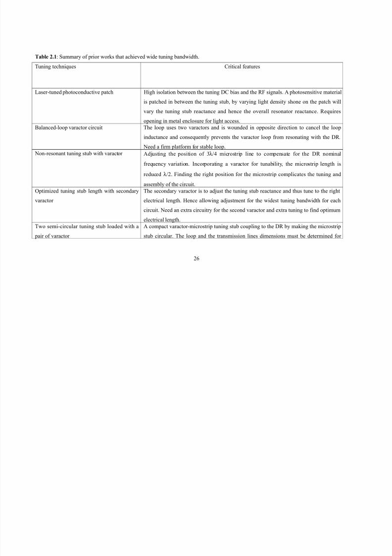
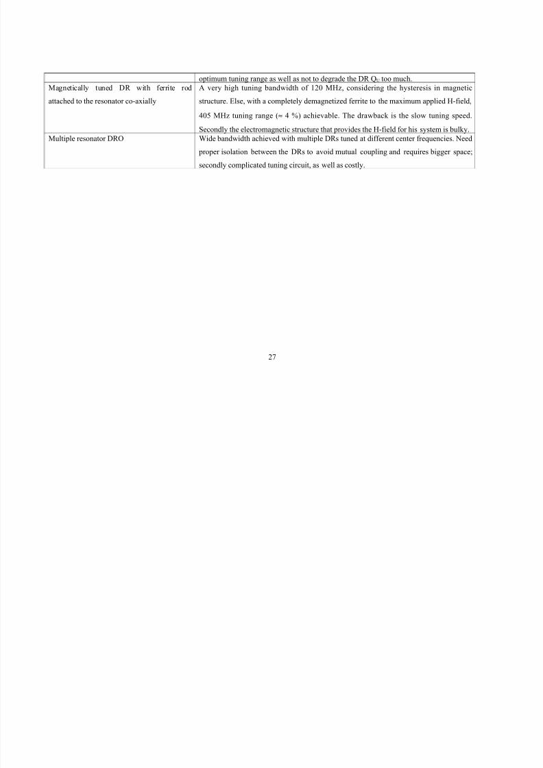
Ta/e 0.1: Summary of prior works that achieved wide tuning bandwidth.
)uning techni-ues +ritical features
%aser9tuned photoconductive patch igh isolation between the tuning D+ bias and the 7 signals. A photosensitive material
is patched in between the tuning stub, by varying light density shone on the patch will
vary the tuning stub reactance and hence the overall resonator reactance. 7e-uires
opening in metal enclosure for light access.
*alanced9loop varactor circuit )he loop uses two varactors and is wounded in opposite direction to cancel the loop
inductance and conse-uently prevents the varactor loop from resonating with the D7.
eed a firm platform for stable loop.
on9resonant tuning stub with varactor Ad3usting the position of /λB> microstrip line to compensate for the D7 nominal
fre-uency variation. Incorporating a varactor for tunability, the microstrip length is
reduced λB. inding the right position for the microstrip complicates the tuning and
assembly of the circuit.
ptimi2ed tuning stub length with secondary
varactor
)he secondary varactor is to ad3ust the tuning stub reactance and thus tune to the right
electrical length. ence allowing ad3ustment for the widest tuning bandwidth for each
circuit. eed an e!tra circuitry for the second varactor and e!tra tuning to find optimum
electrical length.
)wo semi9circular tuning stub loaded with a
pair of varactor
A compact varactor9microstrip tuning stub coupling to the D7 by making the microstrip
stub circular. )he loop and the transmission lines dimensions must be determined for
0
8/11/2019 2_template Fyp Final Report4
http://slidepdf.com/reader/full/2template-fyp-final-report4 26/75
optimum tuning range as well as not to degrade the D7 8F too much.
$agnetically tuned D7 with ferrite rod
attached to the resonator co9a!ially
A very high tuning bandwidth of = $2, considering the hysteresis in magnetic
structure. Else, with a completely demagneti2ed ferrite to the ma!imum applied 9field,
>; $2 tuning range 4≈ > ?6 achievable. )he drawback is the slow tuning speed.
Secondly the electromagnetic structure that provides the 9field for his system is bulky.
$ultiple resonator D7 "ide bandwidth achieved with multiple D7s tuned at different center fre-uencies. eed
proper isolation between the D7s to avoid mutual coupling and re-uires bigger space#
secondly complicated tuning circuit, as well as costly.
H
8/11/2019 2_template Fyp Final Report4
http://slidepdf.com/reader/full/2template-fyp-final-report4 27/75
CHAPTER 3
3 METHODOLOGY
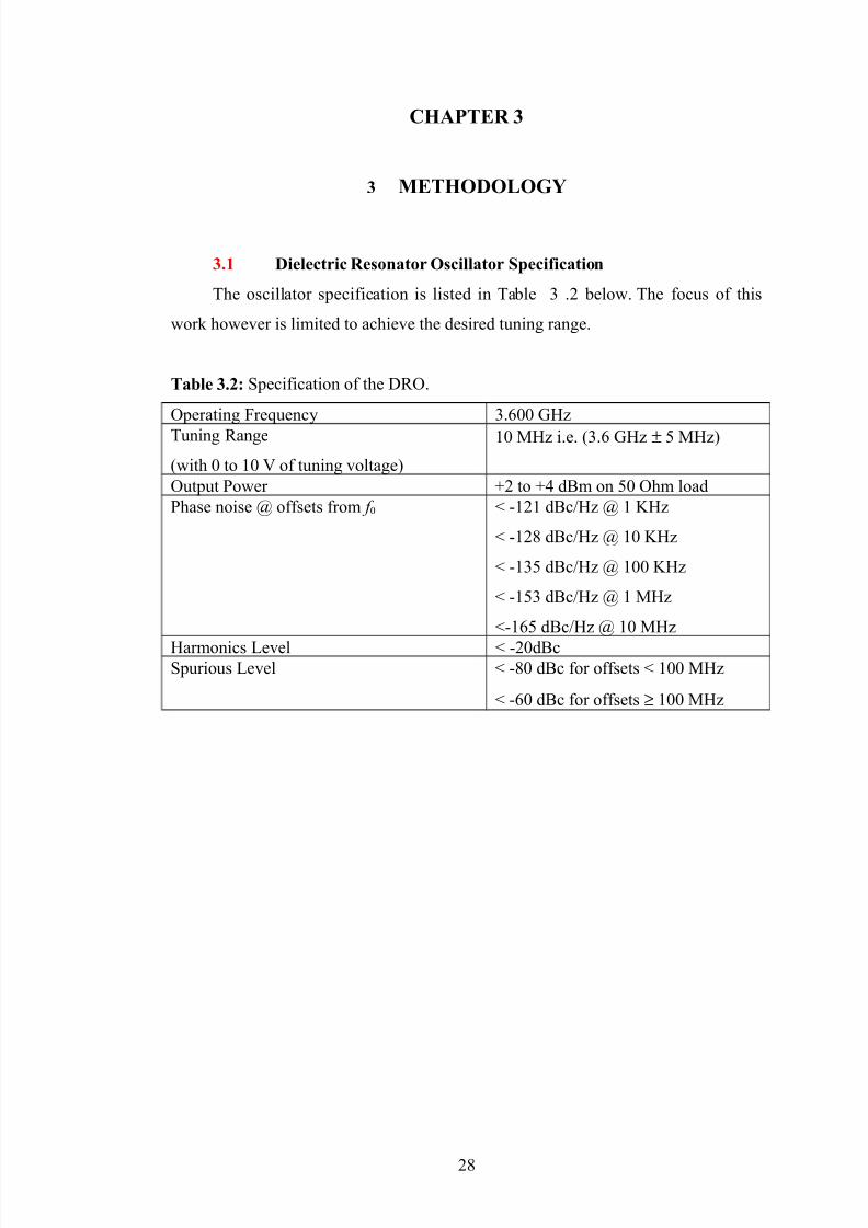
3.1 D"e/e*!"* Re($a! O(*"//a! S5e*"9"*a!"$
)he oscillator specification is listed in )able / . below. )he focus of this
work however is limited to achieve the desired tuning range.
Ta/e 3.0; Specification of the D7.
perating re-uency /.0 12
)uning 7ange
4with to = C of tuning voltage6
= $2 i.e. 4/.0 12 ± ; $26
utput <ower T to T> d*m on ; hm load
<hase noise X offsets from f P 9== d*cB2 X = &2
P 9= d*cB2 X = &2
P 9=/; d*cB2 X = &2
P 9=;/ d*cB2 X = $2
P9=0; d*cB2 X = $2
armonics %evel P 9d*cSpurious %evel P 9 d*c for offsets P = $2
P 90 d*c for offsets ≥ = $2
8/11/2019 2_template Fyp Final Report4
http://slidepdf.com/reader/full/2template-fyp-final-report4 28/75
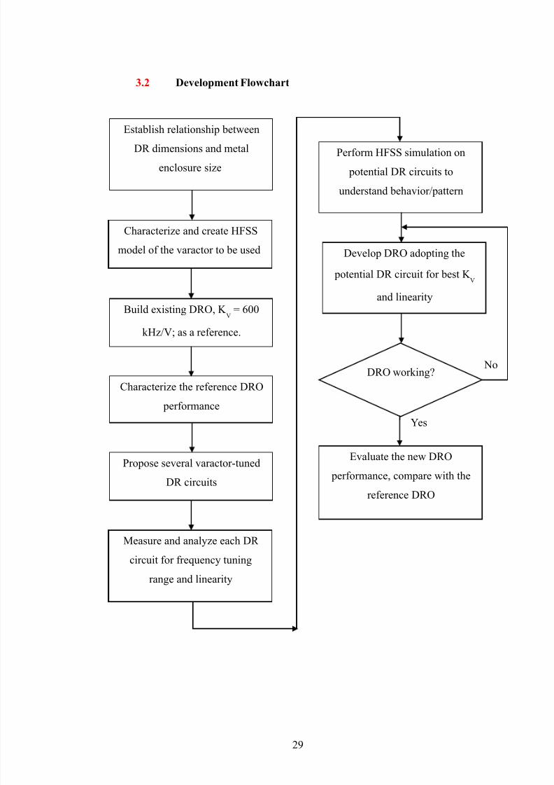
3.0 De#e/52e$! F/,*&a!
J
*uild e!isting D7, & C 0
k2BC# as a reference.
+haracteri2e the reference D7
performance
<ropose several varactor9tuned
D7 circuits
$easure and analy2e each D7
circuit for fre-uency tuning
range and linearity
<erform SS simulation on
potential D7 circuits to
understand behaviorBpattern
Develop D7 adopting the
potential D7 circuit for best & C
and linearity
Establish relationship between
D7 dimensions and metal
enclosure si2e
+haracteri2e and create SS
model of the varactor to be used
D7 workingY
Evaluate the new D7
performance, compare with the
reference D7
Ges
o
8/11/2019 2_template Fyp Final Report4
http://slidepdf.com/reader/full/2template-fyp-final-report4 29/75
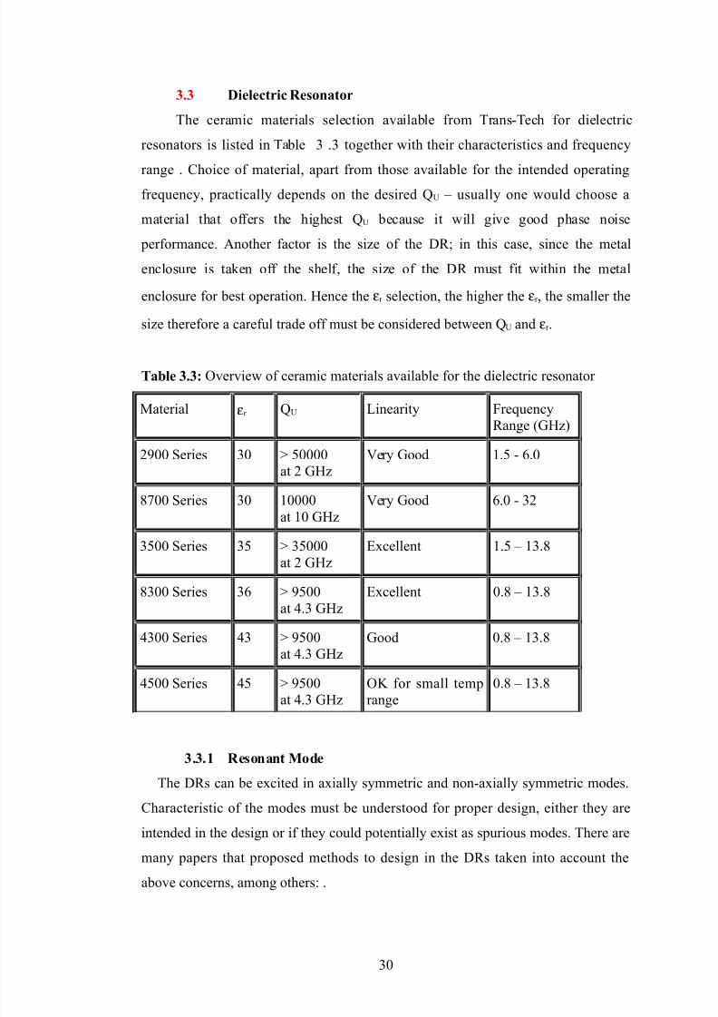
3.3 D"e/e*!"* Re($a!
)he ceramic materials selection available from )rans9)ech for dielectric
resonators is listed in )able / ./ together with their characteristics and fre-uency
range . +hoice of material, apart from those available for the intended operating
fre-uency, practically depends on the desired 8F @ usually one would choose a
material that offers the highest 8F because it will give good phase noise
performance. Another factor is the si2e of the D7# in this case, since the metal
enclosure is taken off the shelf, the si2e of the D7 must fit within the metal
enclosure for best operation. ence the εr selection, the higher the εr , the smaller the
si2e therefore a careful trade off must be considered between 8F and εr .
Ta/e 3.3; verview of ceramic materials available for the dielectric resonator
$aterial εr 8F %inearity re-uency
7ange 4126
J Series / Q ;
at 12
Cery 1ood =.; 9 0.
H Series / =
at = 12
Cery 1ood 0. 9 /
/; Series /; Q /;
at 12
E!cellent =.; @ =/.
/ Series /0 Q J;
at >./ 12
E!cellent . @ =/.
>/ Series >/ Q J;
at >./ 12
1ood . @ =/.
>; Series >; Q J;
at >./ 12
& for small temp
range
. @ =/.
3.3.1 Re($a$! M+e
)he D7s can be e!cited in a!ially symmetric and non9a!ially symmetric modes.
+haracteristic of the modes must be understood for proper design, either they are
intended in the design or if they could potentially e!ist as spurious modes. )here are
many papers that proposed methods to design in the D7s taken into account the
above concerns, among others: .
/

8/11/2019 2_template Fyp Final Report4
http://slidepdf.com/reader/full/2template-fyp-final-report4 30/75
As mentioned above, the D7 can be e!cited in various modes but the principle
transverse electric, )E=O mode, as shown in igure / . 4b6 and 4c6 will be
employed in this oscillator design as it conveniently couples to microstrip
transmission lines, in which a signal propagates in )E$ mode. )he calculation will
use cylindrical coordinates when involving the D7 because the shape is cylindrical
as shown in igure / . 4a6. A rectangular shape D7 is also possible because the
principle resonant mode is also )E=δ . +ylindrical shape is chosen for its physical
symmetry in 29a!is as shown in igure / . 4a6 allowing consistent magnetic field
coupling alongside a microstrip line as depicted in igure / ./.
4a6
4b6 4c6
F"g'e 3.0; A cylindrical D7 with )E=O mode, 4b6 top view and 4c6 side view, in the
case where % P D .
)he wavelength in the dielectric material, λd also called as the guide wavelength, is
given in
r d ε λ λ = 3.1
where λ is the wavelength in air# thus by e!ploiting the principle resonant mode e.g.
)E=δ, the D7 si2e will be reduced compared to the cavity resonator by the order of
r ε . or a cylindrical D7, )E=δ resonant mode is analogous to circular metallic
cavity resonator )E== resonant mode, whereby the resonant length is half the guide
wavelength. )he D7 height 4%6 thus must be on the order of one resonant length inthe dielectric material for it to operate in this principle resonant mode. )he
/=
D
ID
%
y
z
xφ ρ
Electric field
$agnetic field
8/11/2019 2_template Fyp Final Report4
http://slidepdf.com/reader/full/2template-fyp-final-report4 31/75
transverse electric 4)E6 mode does not contain electric field in the 29a!is direction#
the first two subscripts, namely the '( and '=( describe the standing wave 4half9
sinusoid6 pattern in circumferential, φ and radial, ρ directions respectively# and the
third subscript, 'δ(, given by
=A <= d L λ δ 3.0
denotes the fact that there is no complete half9sinusoid pattern within the D7 in 29
a!is direction 4refer to igure / . 4a66 as oppose to circular metallic cavity
resonators. or the D7 to resonate in )E=δ mode , the ratio of its outer diameter, D
to its thickness or height, % must be such that,
>A.=>
L
OD 3.3
and specifically the ratio must be kept
//./A << L
OD 3.4
to minimise interference of spurious modes .
3.4 Re($a$*e S!'*!'e C$(!'*!"$
)he design begins with the analysis of the D7 passive resonant structure. )heresonant structure includes the electrical circuit as well as the metal enclosure as
shown in . )he metal enclosure is to provide shielding. )he resonant structure
electrical e-uivalent circuit is analogous to a single order band9pass filter, with the
D7 as the filter element coupled to transmission lines as the input and output ports.
<recisely, the resonant structure is three9dimensional and apart from the D7, the
varactor, the metal tuning disc and the metal enclosure would affect the resonant
fre-uency. )he varactor coupling to the D7 will be discussed in details in section
/.>.;.
Secondly, the cost constraint imposed on the design compels the use of 'off9the9
shelf( metal enclosure and the incorporated metal tuning disc, resonator assembly @
plastic screw and ceramic support which are leveraged from another circuit
4operating at different fre-uency6.
/
8/11/2019 2_template Fyp Final Report4
http://slidepdf.com/reader/full/2template-fyp-final-report4 32/75
3.4.1 Me!a/ E$*/('e E99e*! $ Re($a$! M+e a$+ Fe8'e$*)
+ohn suggested that the enclosure must be appro!imately twice the biggest
dimension of the D7 so as not to degrade its 8 F resulting from the current induced
on the enclosure surface by the e!ternal field of the D7# and that this e!ternal field
disturbance also changes the resonant fre-uency . Alternatively, )rans9)ech
recommends the enclosure si2e to be three times the D7 si2e, i.e. 4with reference to
6, the enclosure height is,
L L L L /A=
=++ 3.
"here %= is the distance from the ground plane on bottom enclosure to the bottom
of the D7# % is the D7 height and % is the distance from the top of the D7 to the top
enclosure#
and the enclosure length or width,
( )ODW /= 3.6.
)he 'off9the9shelf( metal enclosure dimensions are shown in )able / .>. )he D7
<+* is resting on the bottom enclosure# and another <+* 4containing the rest of
circuitry6 about 0 mils thick 4.H0 mm6 is sandwiched between the top and bottom
enclosure, so the total height, 4 A= L L L ++ 6 of the enclosure is appro!imately =>.
mm.
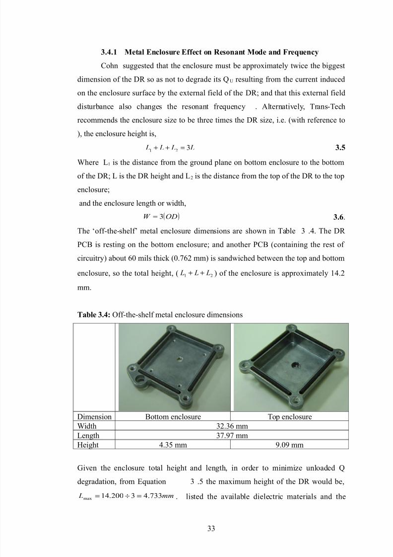
Ta/e 3.4; ff9the9shelf metal enclosure dimensions
Dimension *ottom enclosure )op enclosure
"idth /./0 mm
%ength /H.JH mm
eight >./; mm J.J mm
1iven the enclosure total height and length, in order to minimi2e unloaded 8
degradation, from E-uation / .; the ma!imum height of the D7 would be,
mm L H//.>/A::.=>ma!
=÷= . listed the available dielectric materials and the
//

8/11/2019 2_template Fyp Final Report4
http://slidepdf.com/reader/full/2template-fyp-final-report4 33/75
calculated guide wavelength at /.0 12. )he material that gives the guide
wavelength closest to %ma! will be selected for the research. rom E-uation /.0 the
ma!imum outer diameter would be, mmOD 0;H.=A/JH:./Hma!
=÷= .
Ta/e 3.; +alculated waveguide resonant wavelength, λdB for available materials .
$aterial εr ABd λ 4mm6
J Series / H.0
H Series / H.0
/; Series /; H./
/ Series /0 0.J>
>/ Series >/ 0./;
>; Series >; 0.H
"ith all the re-uirements presented above#
i. the enclosure total dimensions,
ii. calculated ma!imum resonator length or height 4%ma!6,
iii. the resonant wavelengths in the available materials as shown in ,
iv. conditions stated in E-uations / ./ and / .> for operation at /.0
12,
the >; Series material, which is made of 2irconium titanate based ceramic is
selected for this design because with its highest dielectric constant, εr >;, it is
e!pected to yield the smallest dimensions D7 that can satisfy the re-uirements i @ iv
above. )he >; series electrical properties are shown in . )he enclosure dimensions
and the selected material information are feedback to the manufacturer to fabricate
D7.
Ta/e 3.6; Electrical properties of >; series dielectric resonator fabricated for this
design, based on the manufacturer measurement.
Dielectric constant, εr >;.H ± =.;
Fnloaded 8, 8F Q at Z /.; 12
)emperature coefficient of resonant fre-uency T/ <<$B°+ ± = <<$B°+
)he D7 manufacturer, )rans9)ech specifies accuracy within ± = $2 from f +. )he
final D7 dimensions were arrived at after two iterations of samples# the first D7 sample has a height about 0.>HH mm @ the initial D7 si2e is calculated by the
/>
8/11/2019 2_template Fyp Final Report4
http://slidepdf.com/reader/full/2template-fyp-final-report4 34/75
manufacturer based on our application, i.e. the desired f +, enclosure si2e. )he sample
was assembled in the resonant structure shown in and the resonant fre-uency, f + was
measured. If the resonant fre-uency is not within /.0 12 ± = $2 target and
knowing how much it is off target, the ne!t sample is re-uested with accordingdimensions ad3ustment. )he iteration continues until the resonant fre-uency is
within the target. )he final fabricated D7 dimensions are shown in )able / .H# this
yields a nominal f + of /.0 12 ± = $2 when the resonant structure is
measured.
Ta/e 3.=; abricated dielectric resonator physical dimensions.
uter diameter, D 4mm6 =>.J0 ± .;Inner diameter, ID 4mm6 /.J T ./ B 9.
eight, % 4mm6 ;.0=/ nominal
ote that the D7 height is 3ust ;.0=/ mm, compared to calculated resonant
wavelength listed in , i.e. 0.H mm. rom E-uation /., this gives a δ figure of
.J>. )he discussion in this section shows the significant influence of the metal
enclosure on the D7 dimensions and hence the resonant mode as well as the
resonant fre-uency. 1iven the metal enclosure dimensions as the constraint, the D7
fabrication has to be tailored around this constraint.
3.4.0 DR C'5/"$g ! M"*(!"5
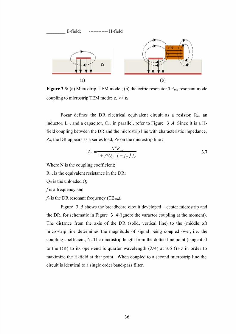
)he signal propagates in microstrip transmission line in almost )E$ mode,
where the electric field 4E9field6 and the 9field are orthogonal to each other and to
the direction of signal propagation. As mentioned in Section /./.=, the D7 is e!cited
in )E=δ where the 9field outside the D7 bears a resemblance to the like of a!ial
magnetic dipole, refer to igure / . 4c6. )his fundamental resonant mode is adopted
in many works and researches .
"hen a D7 e!cited in )E=δ is placed in close pro!imity to a microstrip line, a signal
whose fre-uency is the same as the D7 resonant fre-uency 4in )E=δ mode6 can be
coupled from the microstrip line to the D7 via the 9field as shown in igure / ./
4b6.
/;
8/11/2019 2_template Fyp Final Report4
http://slidepdf.com/reader/full/2template-fyp-final-report4 35/75
[[[[[[[[ E9field# 999999999999 9field
4a6 4b6
F"g'e 3.3; 4a6 $icrostrip, )E$ mode # 4b6 dielectric resonator )E=δ resonant mode
coupling to microstrip )E$ mode# ε QQ ε=
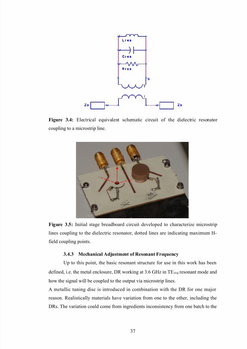
<o2ar defines the D7 electrical e-uivalent circuit as a resistor, 7 res aninductor, %res and a capacitor, +res in parallel, refer to igure / .>. Since it is a 9
field coupling between the D7 and the microstrip line with characteristic impedance,
\, the D7 appears as a series load, \D on the microstrip line :
( ) C C U
res D
f f f Q j
R N Z
−+
=
A=
A
3.=
"here is the coupling coefficient#
7 res is the e-uivalent resistance in the D7#8F is the unloaded 8#
f is a fre-uency and
f + is the D7 resonant fre-uency 4)E=δ6.
igure / .; shows the breadboard circuit developed @ center microstrip and
the D7, for schematic in igure / .> 4ignore the varactor coupling at the moment6.
)he distance from the a!is of the D7 4solid, vertical line6 to the 4middle of6
microstrip line determines the magnitude of signal being coupled over, i.e. the
coupling coefficient, . )he microstrip length from the dotted line point 4tangential
to the D76 to its open9end is -uarter wavelength 4λB>6 at /.0 12 in order to
ma!imi2e the 9field at that point . "hen coupled to a second microstrip line the
circuit is identical to a single order band9pass filter.
/0
ε=
ε
8/11/2019 2_template Fyp Final Report4
http://slidepdf.com/reader/full/2template-fyp-final-report4 36/75
F"g'e 3.4; Electrical e-uivalent schematic circuit of the dielectric resonator coupling to a microstrip line.
F"g'e 3.; Initial stage breadboard circuit developed to characteri2e microstrip
lines coupling to the dielectric resonator, dotted lines are indicating ma!imum 9
field coupling points.
3.4.3 Me*&a$"*a/ A+'(!2e$! 9 Re($a$! Fe8'e$*)
Fp to this point, the basic resonant structure for use in this work has been
defined, i.e. the metal enclosure, D7 working at /.0 12 in )E=δ resonant mode and
how the signal will be coupled to the output via microstrip lines.
A metallic tuning disc is introduced in combination with the D7 for one ma3or
reason. 7ealistically materials have variation from one to the other, including the
D7s. )he variation could come from ingredients inconsistency from one batch to the
/H
8/11/2019 2_template Fyp Final Report4
http://slidepdf.com/reader/full/2template-fyp-final-report4 37/75
other and machining accuracy limitation, to name a few. )hus, the D7 is
manufactured such that its natural resonant fre-uency falls within certain tolerance
from specified nominal fre-uency. Some sort of compensation is re-uired to cater
for this material variation.
A metal tuning disc is placed above the D7, i.e. screwed in to the top of the
metal enclosure, with the tuning disc position in vertical 429a!is6 a!is ad3ustable. )he
tolerance in the D7 resonant fre-uency is compensated by ad3usting the distance
between the tuning disc and the D7, namely % in . )his is done manually by turning
the metal disc screw top. "hen the metal tuning disc is moved towards the D7, the
resonant fre-uency varies proportional to the stored magnetic and electric energies
of the displaced volume .
F"g'e 3.6; Simplified assembly of the D7 resonant structure
)he mounting of the D7 on a ceramic support on top of the laminate or the
<+* is to give reasonable distance from the metal enclosure, i.e. the distances % =
and %. Although this is insufficient due to the small enclosure height and will
potentially degrade some performance aspects of the D7 like phase noise , it is a
compromise given the available metal enclosures.
3.4.4 E/e*!$"* T'$"$g E/e2e$! % Vaa*!
A varactor diode is introduced into the D7 circuit as the electronic tuning
element to ad3ust the fre-uency. )he oscillator <%% uses the tuning element to ad3ust
/
D%
%D7
%=
support
$etal enclosure4grounded6
$etal tuning disc
$icrowave laminate
Screw top
"
8/11/2019 2_template Fyp Final Report4
http://slidepdf.com/reader/full/2template-fyp-final-report4 38/75
the phase and fre-uency of the oscillator. )his D7 application as a local oscillator
4%6 means it is a fi!ed fre-uency oscillator. )he <%% is to maintain accurately the
output signal fre-uency whereby the oscillator fre-uency drifts due to temperature
fluctuation and the devices aging.
As for free running oscillator, any varactor with high capacitance ratio seems
reasonable, regardless of the tuning linearity. owever, when considering
incorporating a <%% for the oscillator control system, tuning linearity has significant
effect on the loop filter or the loop controller. urthermore, since this D7 is a fi!ed
fre-uency application with a relatively narrow tuning bandwidth compared to
voltage controlled oscillators 4C+(s6, it would be redundant to have a comple!
<%%, i.e. with selectable loop controller response to cater for different tuning
sensitivity. ote that the tuning linearity or sensitivity 4& C, unit 2BC6 here is the
slope of the fre-uency against varactor tuning voltage 4v tune6 plot.
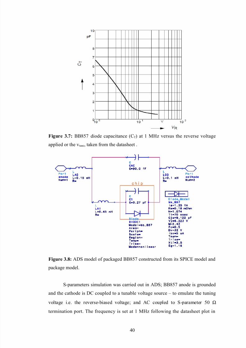
3.4.4.1 BB>= Vaa*! ADS 2+e/
**;H, a silicon hyperabrupt varactor from Infineon )echnologies is
adopted for this D7 design. Its small profile S+D package means it has very
low parasitic elements# A<<EDIL * shows the electrical e-uivalent circuit of the package. igure / .H shows the capacitance range from vtune = C to about C #
the tuning voltage specified for the D7 is from C @ = C. **;H S<I+E chip
model and its package model as shown in igure / ., are used to simulate the
capacitance at C @ = C vtune and characteri2e the varactor. )he chip S<I+E model
can be referred in A<<EDIL A. Since the model will be used in the circuit design
and simulation, the **;H packaged model was simulated upfront in circuit
simulator Agilent Advanced Design System 4ADS6. Fsing ADS model which allows
the variation of the reverse9biased voltage, i.e. vtune, the capacitance of the varactor at
a particular biased voltage can be deduced accurately.
/J
8/11/2019 2_template Fyp Final Report4
http://slidepdf.com/reader/full/2template-fyp-final-report4 39/75
F"g'e 3.=; **;H diode capacitance 4+)6 at = $2 versus the reverse voltage
applied or the vtune, taken from the datasheet .
F"g'e 3.>; ADS model of packaged **;H constructed from its S<I+E model and
package model.
S9parameters simulation was carried out in ADS# **;H anode is grounded
and the cathode is D+ coupled to a tunable voltage source @ to emulate the tuning
voltage i.e. the reverse9biased voltage# and A+ coupled to S9parameter ; Ωtermination port. )he fre-uency is set at = $2 following the datasheet plot in
>
8/11/2019 2_template Fyp Final Report4
http://slidepdf.com/reader/full/2template-fyp-final-report4 40/75
igure / .H. )he S== data is plotted on the impedance chart 4Smith +hart6 for every
vtune from C @ = C at = C interval. )he capacitance at each v tune is derived from
( )( )ImA= C Z F C ⋅= π , where F is = $2 and \+4Im6 is the varactor reactance at =
$2. )he ADS simulation result of the packaged **;H is showed in igure / .J.
)he simulation shows the **;H capacitance is in good agreement with the
datasheet plot in igure / .H. )he data for ADS and E$DS simulations are listed in
A<<EDIL +.
3.4.4.0 BB>= EMDS 2+e/
E$DS is an electromagnetic field simulator for two and three dimensional
passive structures. )he D7 resonant circuit involves many three dimensional
structures like the resonator itself, the ceramic support, the metal enclosure, the
tuning disc besides the planar microstrip transmission lines. f all the above, only
the microstrips and the varactor can be readily modeled in ADS circuit simulator.
)he three dimensional structures are rather complicated to model accurately in ADS,
one main reason is because of the three dimensional electromagnetic field
interaction among the structures of different electrical properties, which is definitely
inade-uate to 3ust model their coupling using transformers or baluns. ence the
application of E$DS simulator, inadvertently the varactor which is part of the three
dimensional tunable resonant circuit has to be modeled in E$DS too.
Since E$DS only support passive electrical structures, the varactor which
re-uires biasing, has to be modeled as a passive capacitor somehow. rom the ADS
result, the capacitance value at a particular biased voltage is known. Secondly, for a
passive capacitor, its capacitance depends on its dielectric material i.e. the dielectric
constant, εr . )hus, and by keeping other capacitance variables 4surface area and
distance between the metal plates6 constant, to emulate the varactor capacitance at a
particular biased voltage, its dielectric constant is set to achieve the desired
capacitance @ setting the dielectric constant can be done in E$DS when defining the
properties of a material. owever this method is not so straight forward. )he E$DS
simulations are swept at = $2 since capacitances obtained from ADS are also
swept at = $2, following the reference data from the datasheet 4igure / .H6. )he
E$DS results are displayed as impedance on a Smith chart, the capacitance 4+6 is
>=
8/11/2019 2_template Fyp Final Report4
http://slidepdf.com/reader/full/2template-fyp-final-report4 41/75
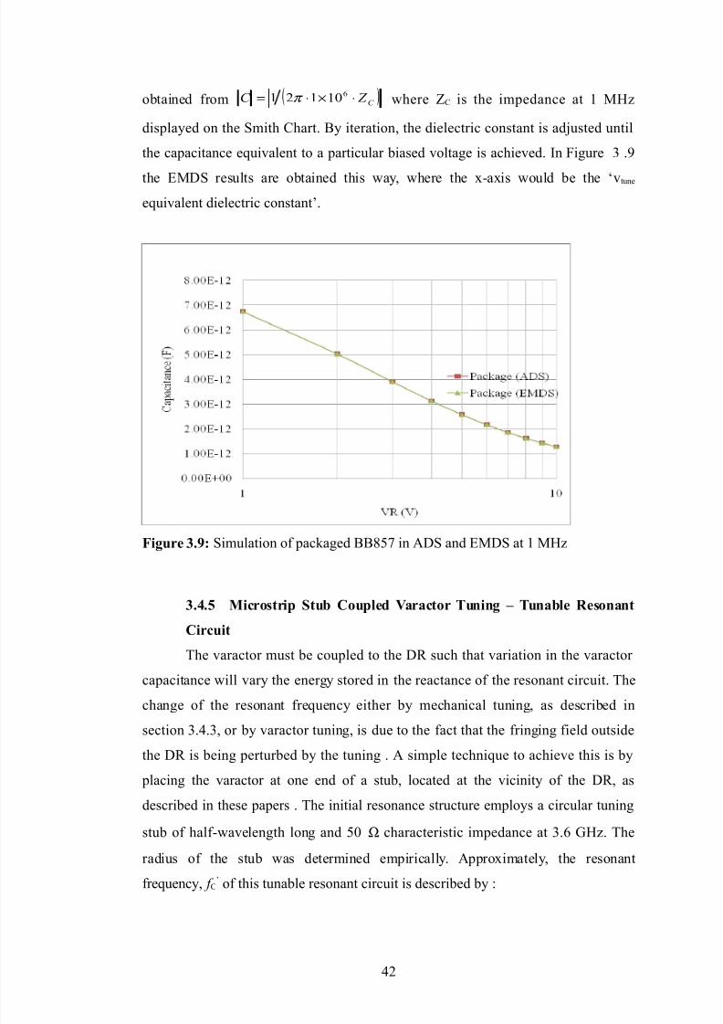
obtained from ( )C
Z C ⋅×⋅= 0
=:=A= π where \+ is the impedance at = $2
displayed on the Smith +hart. *y iteration, the dielectric constant is ad3usted until
the capacitance e-uivalent to a particular biased voltage is achieved. In igure / .J
the E$DS results are obtained this way, where the !9a!is would be the 'vtune
e-uivalent dielectric constant(.
F"g'e 3.?; Simulation of packaged **;H in ADS and E$DS at = $2
3.4. M"*(!"5 S!' C'5/e+ Vaa*! T'$"$g % T'$a/e Re($a$!
C"*'"!
)he varactor must be coupled to the D7 such that variation in the varactor
capacitance will vary the energy stored in the reactance of the resonant circuit. )he
change of the resonant fre-uency either by mechanical tuning, as described in
section /.>./, or by varactor tuning, is due to the fact that the fringing field outside
the D7 is being perturbed by the tuning . A simple techni-ue to achieve this is by
placing the varactor at one end of a stub, located at the vicinity of the D7, as
described in these papers . )he initial resonance structure employs a circular tuning
stub of half9wavelength long and ; Ω characteristic impedance at /.0 12. )he
radius of the stub was determined empirically. Appro!imately, the resonant
fre-uency, f +( of this tunable resonant circuit is described by :
>
8/11/2019 2_template Fyp Final Report4
http://slidepdf.com/reader/full/2template-fyp-final-report4 42/75
( )
++
=resT
T resC C
L L N
C C N f f
B=
B=
A
A
AAU 3.>
"here f + is the D7 resonant fre-uency#
is the coupling coefficient between the D7 and varactor#
+res is the D7 e-uivalent capacitance#
+) is the varactor capacitance#
%res is the D7 e-uivalent inductance and
%) is the tuning stub inductance.
"ith the varactor capacitance set at a value e-uivalent to 'v tune of ; C(, the tunable
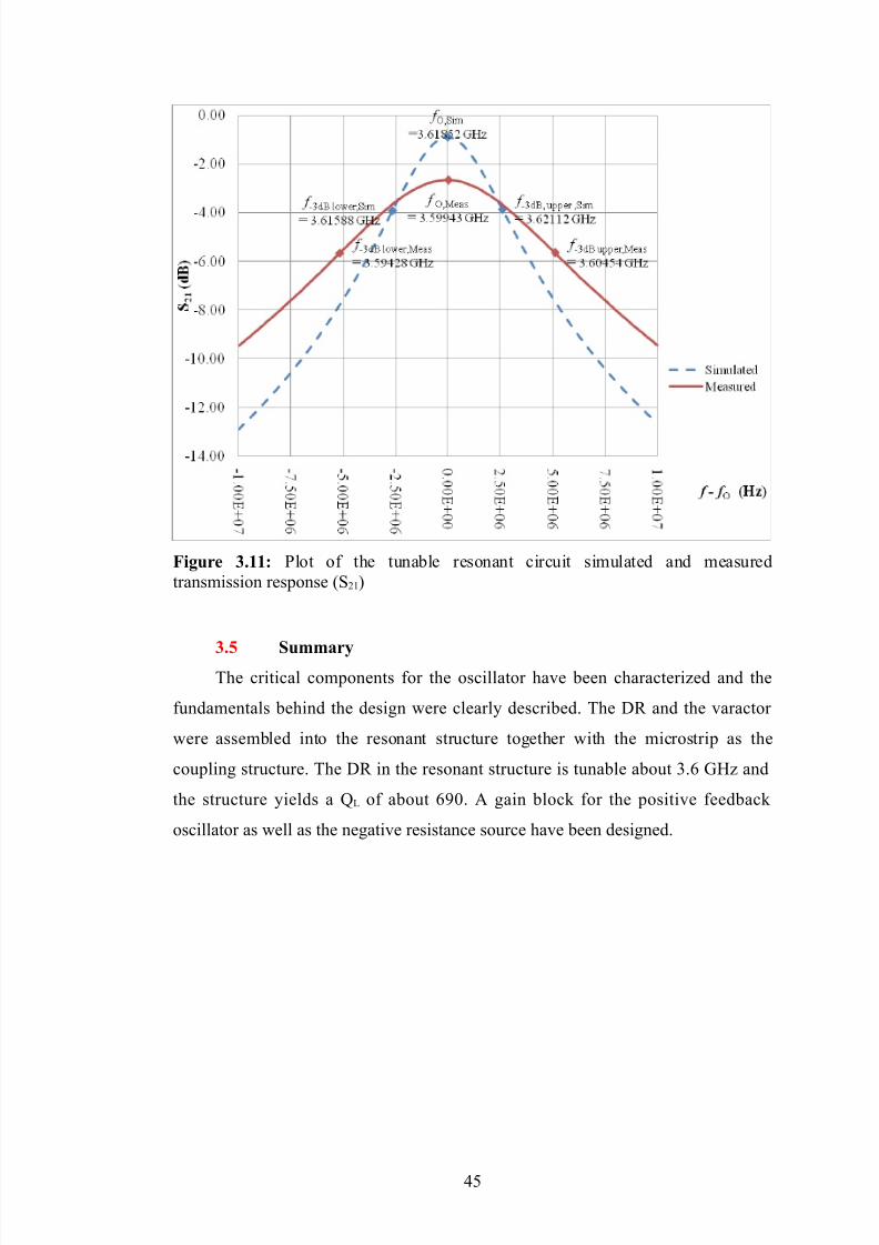
resonant circuit was simulated in E$DS for the transmission response 4S=6, the plotis shown in igure / .==, the resonant fre-uency is at /.0=; 12.
or this simulation, 8% of the resonant circuit with a load of ; Ω is,
( ) ;;H/.0J:
=:0=;./0A==A./
=:0=;A./
J
J
//
=×−
×=
−=
−− dBlowdBup
O L
f f
f Q
and the predicted resonator half bandwidth is:
MHz Q
f
L
O0A.A
;;H/.0J:A
=:0=;A./
A
J
=×
×= .
*ased on the transmission response measurement, of which the result is also plotted
in igure / .==, the actual resonant circuit 8% and half bandwidth are /;.H/;H and
;.=/ $2 respectively. )he difference between the simulated and measured values
is due to some components which were omitted in the simulation to reduce
processing comple!ity. )hese components such as the S$A connectors, the plastic
screw that locks the D7 in position 4refer to igure / .= 4b66 contribute some losses
and degrade the overall resonant structure 8 factor. Secondly, in actual the varactor
8 factor which is lower than the D7 limits the overall resonant structure 8 factor
and was also not included in the simulation.
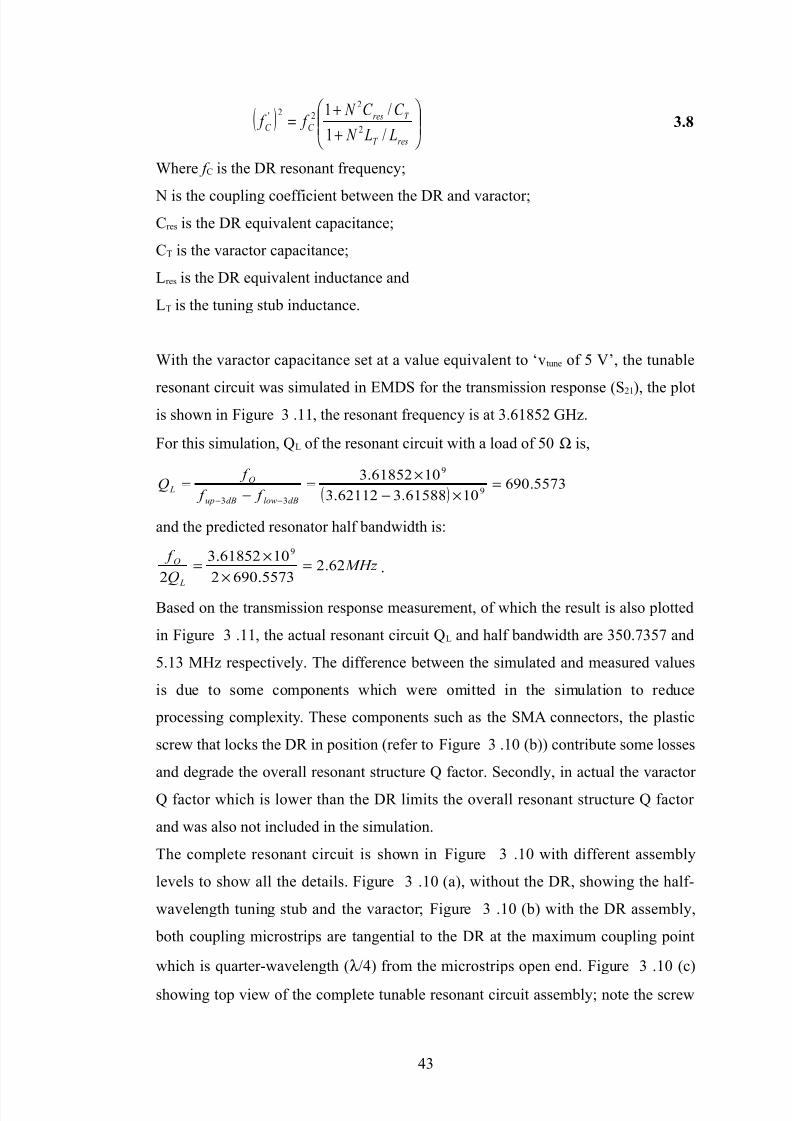
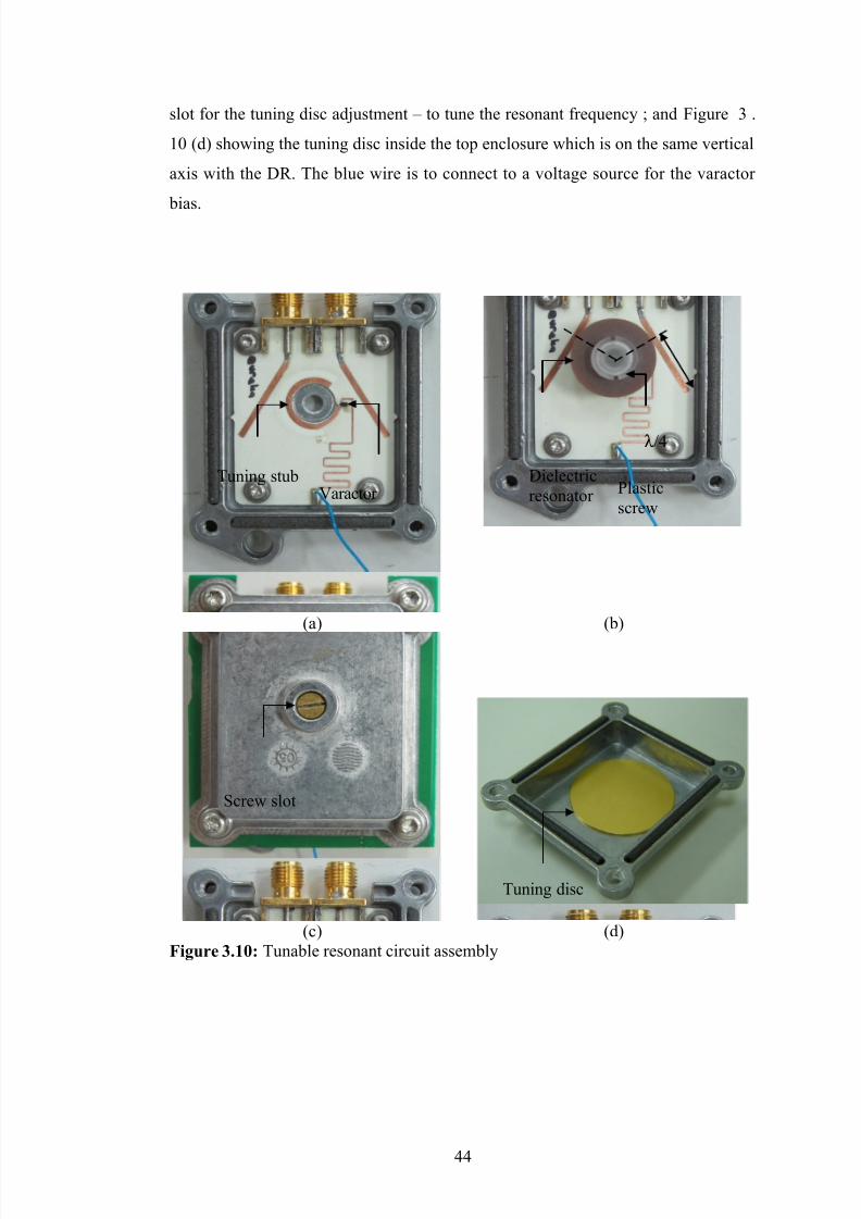
)he complete resonant circuit is shown in igure / .= with different assembly
levels to show all the details. igure / .= 4a6, without the D7, showing the half9
wavelength tuning stub and the varactor# igure / .= 4b6 with the D7 assembly,
both coupling microstrips are tangential to the D7 at the ma!imum coupling point
which is -uarter9wavelength 4λB>6 from the microstrips open end. igure / .= 4c6
showing top view of the complete tunable resonant circuit assembly# note the screw
>/
8/11/2019 2_template Fyp Final Report4
http://slidepdf.com/reader/full/2template-fyp-final-report4 43/75
slot for the tuning disc ad3ustment @ to tune the resonant fre-uency # and igure / .
= 4d6 showing the tuning disc inside the top enclosure which is on the same vertical
a!is with the D7. )he blue wire is to connect to a voltage source for the varactor
bias.
4a6 4b6
4c6 4d6
F"g'e 3.1@; )unable resonant circuit assembly
>>
)uning stubCaractor
λB>
Dielectric
resonator
Screw slot
)uning disc
<lastic
screw
8/11/2019 2_template Fyp Final Report4
http://slidepdf.com/reader/full/2template-fyp-final-report4 44/75
F"g'e 3.11; <lot of the tunable resonant circuit simulated and measured
transmission response 4S=6
3. S'22a))he critical components for the oscillator have been characteri2ed and the
fundamentals behind the design were clearly described. )he D7 and the varactor
were assembled into the resonant structure together with the microstrip as the
coupling structure. )he D7 in the resonant structure is tunable about /.0 12 and
the structure yields a 8% of about 0J. A gain block for the positive feedback
oscillator as well as the negative resistance source have been designed.
>;
8/11/2019 2_template Fyp Final Report4
http://slidepdf.com/reader/full/2template-fyp-final-report4 45/75
8/11/2019 2_template Fyp Final Report4
http://slidepdf.com/reader/full/2template-fyp-final-report4 46/75
F"g'e 4.10; %ayout of the amplifier circuit, the schematic is in A<<EDIL D.
F"g'e 4.13; )he amplifier gain and phase shift measurement setup.
>H
Input port utput port
+apacitive stub +apacitive stub
Inductive stub
7 choke 7 *
*ypass
capacitor
*ipolar transistor
<ower supplyT= CD+
Cector A
1A
λB> at /.0 12
8/11/2019 2_template Fyp Final Report4
http://slidepdf.com/reader/full/2template-fyp-final-report4 47/75
F"g'e 4.14; )he amplifier gain, the markers are showing the gain at /.0 12.
)he amplifier phase shift simulated and measured values are plotted in
igure > .=;, at /.0 12 they are H0.H° and >.H° respectively. *y referring to
igure > .=, the measurement points i.e. the input and output ports are each
distanced by about =.0 mm from the amplifier circuit due to the /.0 12 -uarter9
wavelength stubs originally for the resonant structure. )otal electrical length of the
two stubs is =° at /.0 12, thus deducting this from the measured phase shift,
°=°−° H.=:>=I:H.AI> is the actual phase shift due to the amplifier.
>
8/11/2019 2_template Fyp Final Report4
http://slidepdf.com/reader/full/2template-fyp-final-report4 48/75
F"g'e 4.1; )he amplifier phase shift, the markers are phase shifts at /.0 12.
)he same S9parameters simulation above, 4 m ! C /:≈ 6 gives a noise figure
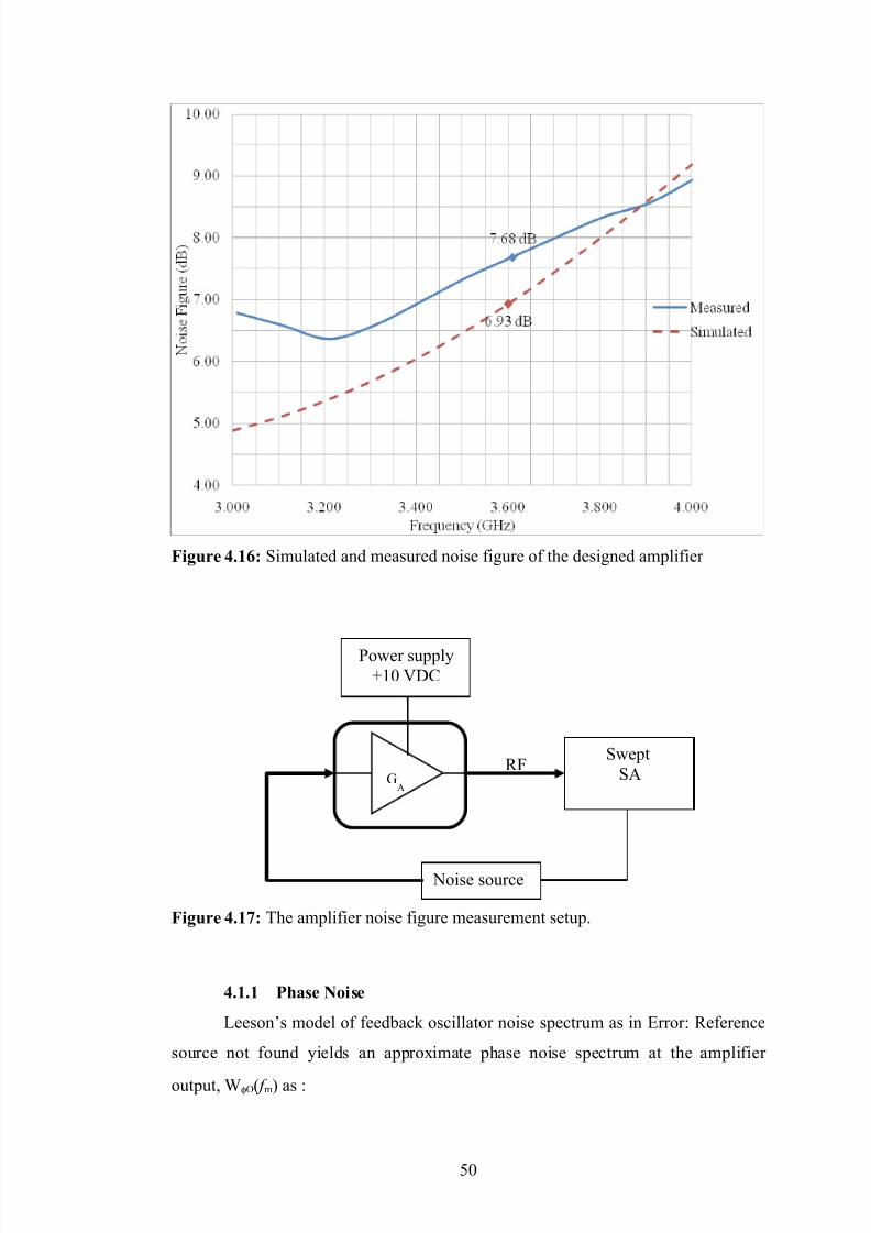
46 of 0.J/ d* as shown above in igure > .=0. )he actual measured is H.0 d*,
measured at a slightly offset fre-uency 4to avoid potential interference from other
/.0 12 signals. )he noise figure measurement setup is shown in # the noise source
4model < />0+6 is driven by the SA 4model Agilent E>>>A with oise igure
option6, its output is fed into the amplifier input and the amplifier output goes into
the SA 7 input. )he SA is set to noise figure mode for the noise figure
measurement.
>J
8/11/2019 2_template Fyp Final Report4
http://slidepdf.com/reader/full/2template-fyp-final-report4 49/75
F"g'e 4.16; Simulated and measured noise figure of the designed amplifier
F"g'e 4.1=; )he amplifier noise figure measurement setup.
4.1.1 P&a(e N"(e
%eeson(s model of feedback oscillator noise spectrum as in Error: 7eference
source not found yields an appro!imate phase noise spectrum at the amplifier
output, "φ4 f m6 as :
;
<ower supply
T= CD+
Swept
SA7
1A
oise source
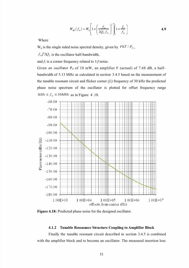
8/11/2019 2_template Fyp Final Report4
http://slidepdf.com/reader/full/2template-fyp-final-report4 50/75
( )
+
+=
mm L
OmO
f
f
f Q
f W f W /
A
=A
=φ φ 4.?
"here
"φ is the single sided noise spectral density, given by O " F#T B ,
LO Q f A is the oscillator half9bandwidth,
and f / is a corner fre-uency related to =B f noise.
1iven an oscillator < of = m", an amplifier 4actual6 of H.0 d*, a half9
bandwidth of ;.=/ $2 as calculated in section /.>.; based on the measurement of
the tunable resonant circuit and flicker corner 4 f /6 fre-uency of / k2 the predicted
phase noise spectrum of the oscillator is plotted for offset fre-uency range
MHz f #Hz m =:= ≤≤ as in igure > .=.
F"g'e 4.1>; <redicted phase noise for the designed oscillator.
4.1.0 T'$a/e Re($a$*e S!'*!'e C'5/"$g ! A25/"9"e B/*<
inally the tunable resonant circuit described in section /.>.; is combined
with the amplifier block and to become an oscillator. )he measured insertion loss
;=
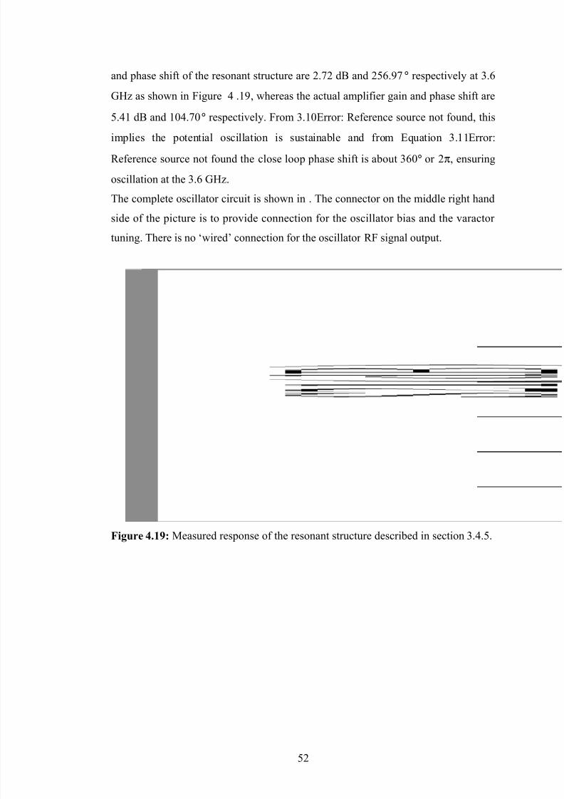
8/11/2019 2_template Fyp Final Report4
http://slidepdf.com/reader/full/2template-fyp-final-report4 51/75
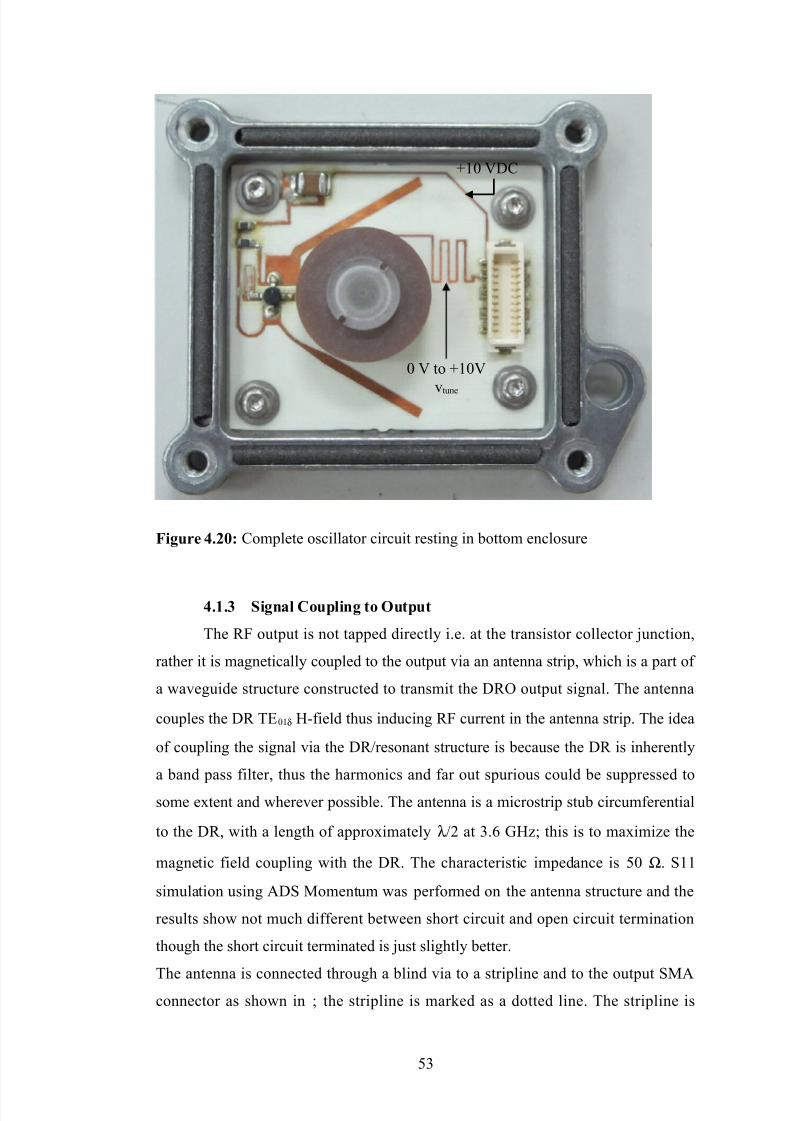
8/11/2019 2_template Fyp Final Report4
http://slidepdf.com/reader/full/2template-fyp-final-report4 52/75
F"g'e 4.0@; +omplete oscillator circuit resting in bottom enclosure
4.1.3 S"g$a/ C'5/"$g ! O'!5'!
)he 7 output is not tapped directly i.e. at the transistor collector 3unction,
rather it is magnetically coupled to the output via an antenna strip, which is a part of
a waveguide structure constructed to transmit the D7 output signal. )he antenna
couples the D7 )E=δ 9field thus inducing 7 current in the antenna strip. )he idea
of coupling the signal via the D7Bresonant structure is because the D7 is inherently
a band pass filter, thus the harmonics and far out spurious could be suppressed to
some e!tent and wherever possible. )he antenna is a microstrip stub circumferential
to the D7, with a length of appro!imately λB at /.0 12# this is to ma!imi2e the
magnetic field coupling with the D7. )he characteristic impedance is ; Ω. S==
simulation using ADS $omentum was performed on the antenna structure and the
results show not much different between short circuit and open circuit termination
though the short circuit terminated is 3ust slightly better.
)he antenna is connected through a blind via to a stripline and to the output S$A
connector as shown in # the stripline is marked as a dotted line. )he stripline is
;/
T= CD+
C to T=C
vtune
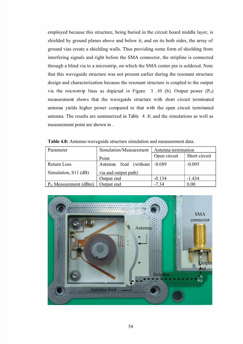
8/11/2019 2_template Fyp Final Report4
http://slidepdf.com/reader/full/2template-fyp-final-report4 53/75
employed because this structure, being buried in the circuit board middle layer, is
shielded by ground planes above and below it# and on its both sides, the array of
ground vias create a shielding walls. )hus providing some form of shielding from
interfering signals and right before the S$A connector, the stripline is connected
through a blind via to a microstrip, on which the S$A center pin is soldered. ote
that this waveguide structure was not present earlier during the resonant structure
design and characteri2ation because the resonant structure is coupled to the output
via the microstrip lines as depicted in igure / .= 4b6. utput power 4<6
measurement shows that the waveguide structure with short circuit terminated
antenna yields higher power compared to that with the open circuit terminated
antenna. )he results are summari2ed in )able > .# and the simulations as well as
measurement point are shown in .
Ta/e 4.>; Antenna9waveguide structure simulation and measurement data.
<arameter SimulationB$easurement
<oint
Antenna termination
pen circuit Short circuit
7eturn %oss
Simulation, S== 4d*6
Antenna feed 4without
via and output path6
9.J 9.J;
utput end 9.=/> 9=.>/>< $easurement 4d*m6 utput end 9H./> .
;>
Antenna
Stripline
S$A
connector
Antenna feed
utput
end

8/11/2019 2_template Fyp Final Report4
http://slidepdf.com/reader/full/2template-fyp-final-report4 54/75
F"g'e 4.01; scillator signal coupling to the output
4.0 I$"!"a/ DRO Pe92a$*e
)he initial D7 that has been designed, as described in Section Error: 7eference
source not found was measured for its f as well as & C, <, harmonics and phase
noise 4"φ4 f m66. Its performance will be the benchmark for subse-uent e!periments.
)he measurement set up for each measurement are also described.
4.0.1 F'$+a2e$!a/ Fe8'e$*) a$+ T'$"$g Se$("!"#"!)
F"g'e 4.00; Spectrum measurement set up.
shows a common measurement set up for power, fre-uency, & C and
harmonics. )he power supply must be a low noise or with good low fre-uency @
kilohert2 to a few tens of megahert2 filtering. )his is particularly importance for
phase noise measurement. or fre-uency accuracy measurement, the general setting
on any SA:
i. Set the display to center at the e!pected f point, i.e. /.0 12,
ii. arrow the span or the SA fre-uency sweep to a few tens of
megahert2 for accurate fre-uency measurement.
iii. Enable the marker function, do a peak search and once the marker is
locked on the signal peak, activate the signal track
)he D7 varactor bias, vtune is set at around T; C, while observing the
reading on the SA for signal around /.0 12, ad3ust tuning disc until the signal is
almost right on /.0 12. A finer ad3ust on v tune i.e. in = mC increment can bring the
signal spot on /.0 12. In the <%% system, the loop controller i.e. the
;;
Dual Coltage
Supply
Swept
SA
T= C D+
C to T= C
tunable D+
7
D7
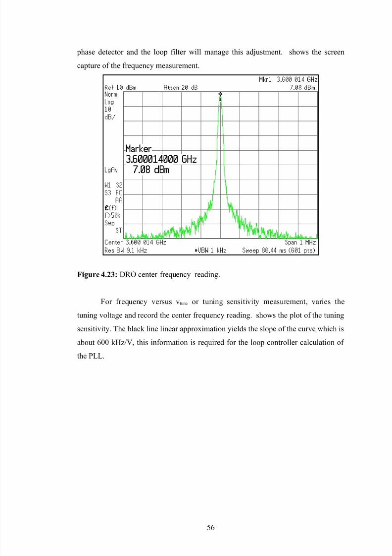
8/11/2019 2_template Fyp Final Report4
http://slidepdf.com/reader/full/2template-fyp-final-report4 55/75
phase detector and the loop filter will manage this ad3ustment. shows the screen
capture of the fre-uency measurement.
F"g'e 4.03; D7 center fre-uency reading.
or fre-uency versus vtune or tuning sensitivity measurement, varies the
tuning voltage and record the center fre-uency reading. shows the plot of the tuning
sensitivity. )he black line linear appro!imation yields the slope of the curve which is
about 0 k2BC, this information is re-uired for the loop controller calculation of
the <%%.
;0
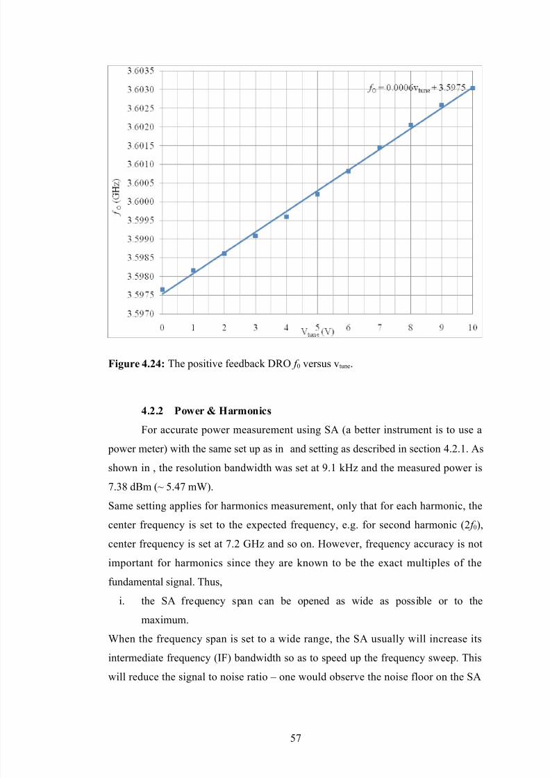
8/11/2019 2_template Fyp Final Report4
http://slidepdf.com/reader/full/2template-fyp-final-report4 56/75
F"g'e 4.04; )he positive feedback D7 f versus vtune.
4.0.0 P,e Ha2$"*(
or accurate power measurement using SA 4a better instrument is to use a
power meter6 with the same set up as in and setting as described in section >..=. As
shown in , the resolution bandwidth was set at J.= k2 and the measured power is
H./ d*m 4Z ;.>H m"6.
Same setting applies for harmonics measurement, only that for each harmonic, the
center fre-uency is set to the e!pected fre-uency, e.g. for second harmonic 4 f 6,
center fre-uency is set at H. 12 and so on. owever, fre-uency accuracy is not
important for harmonics since they are known to be the e!act multiples of the
fundamental signal. )hus,
i. the SA fre-uency span can be opened as wide as possible or to the
ma!imum.
"hen the fre-uency span is set to a wide range, the SA usually will increase its
intermediate fre-uency 4I6 bandwidth so as to speed up the fre-uency sweep. )his
will reduce the signal to noise ratio @ one would observe the noise floor on the SA
;H
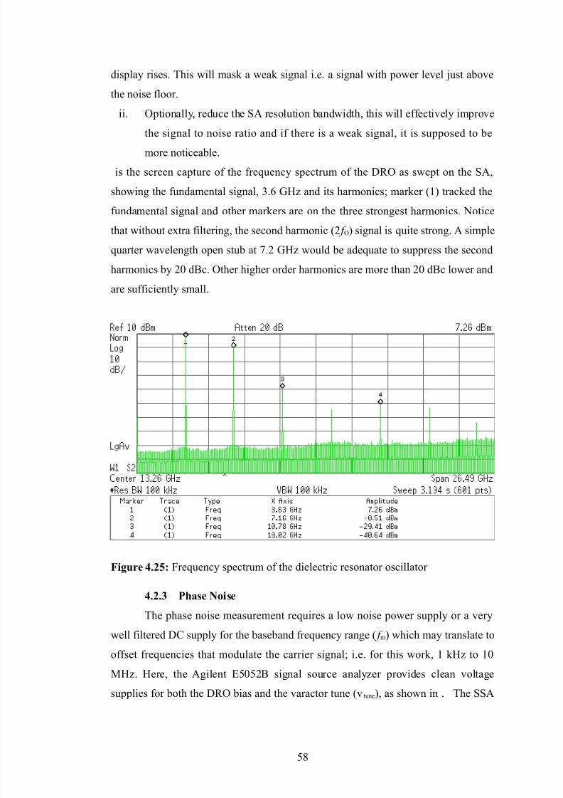
8/11/2019 2_template Fyp Final Report4
http://slidepdf.com/reader/full/2template-fyp-final-report4 57/75
display rises. )his will mask a weak signal i.e. a signal with power level 3ust above
the noise floor.
ii. ptionally, reduce the SA resolution bandwidth, this will effectively improve
the signal to noise ratio and if there is a weak signal, it is supposed to be
more noticeable.
is the screen capture of the fre-uency spectrum of the D7 as swept on the SA,
showing the fundamental signal, /.0 12 and its harmonics# marker 4=6 tracked the
fundamental signal and other markers are on the three strongest harmonics. otice
that without e!tra filtering, the second harmonic 4 f 6 signal is -uite strong. A simple
-uarter wavelength open stub at H. 12 would be ade-uate to suppress the second
harmonics by d*c. ther higher order harmonics are more than d*c lower and
are sufficiently small.
F"g'e 4.0; re-uency spectrum of the dielectric resonator oscillator
4.0.3 P&a(e N"(e
)he phase noise measurement re-uires a low noise power supply or a very
well filtered D+ supply for the baseband fre-uency range 4 f m6 which may translate to
offset fre-uencies that modulate the carrier signal# i.e. for this work, = k2 to =
$2. ere, the Agilent E;;* signal source analy2er provides clean voltage
supplies for both the D7 bias and the varactor tune 4v tune6, as shown in . )he SSA
;
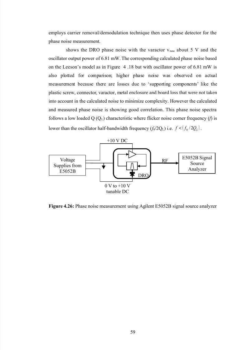
8/11/2019 2_template Fyp Final Report4
http://slidepdf.com/reader/full/2template-fyp-final-report4 58/75
employs carrier removalBdemodulation techni-ue then uses phase detector for the
phase noise measurement.
shows the D7 phase noise with the varactor v tune about ; C and the
oscillator output power of 0.= m". )he corresponding calculated phase noise based
on the %eeson(s model as in igure > .= but with oscillator power of 0.= m" is
also plotted for comparison# higher phase noise was observed on actual
measurement because there are losses due to 'supporting components( like the
plastic screw, connector, varactor, metal enclosure and board loss that were not taken
into account in the calculated noise to minimi2e comple!ity. owever the calculated
and measured phase noise is showing good correlation. )his phase noise spectra
follows a low loaded 8 48%6 characteristic where flicker noise corner fre-uency 4 f 6 is
lower than the oscillator half9bandwidth fre-uency 4 f B8%6 i.e. ( ) LQ f f AB:
< .
F"g'e 4.06; <hase noise measurement using Agilent E;;* signal source analy2er
;J
Coltage
Supplies from
E;;*
E;;* Signal
Source
Analy2er
T= C D+
C to T= C
tunable D+
7
D7
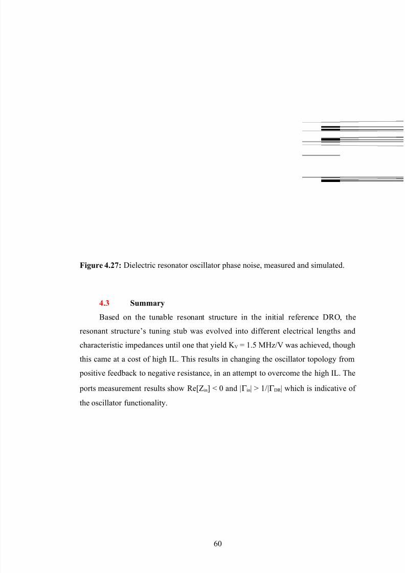
8/11/2019 2_template Fyp Final Report4
http://slidepdf.com/reader/full/2template-fyp-final-report4 59/75
F"g'e 4.0=; Dielectric resonator oscillator phase noise, measured and simulated.
4.3 S'22a)
*ased on the tunable resonant structure in the initial reference D7, the
resonant structure(s tuning stub was evolved into different electrical lengths and
characteristic impedances until one that yield & C =.; $2BC was achieved, though
this came at a cost of high I%. )his results in changing the oscillator topology from
positive feedback to negative resistance, in an attempt to overcome the high I%. )he
ports measurement results show 7eM\inN P and ]Γ in] Q =B]Γ D7 ] which is indicative of
the oscillator functionality.
0
8/11/2019 2_template Fyp Final Report4
http://slidepdf.com/reader/full/2template-fyp-final-report4 60/75
CHAPTER 6
CONCLUSION AND FUTURE WORKS
A high & C D7 design has been proposed which fulfilled the ob3ectives of the
research 4section =./6, there resonant structure is also applicable for band pass filter
design. )wo key parameters of the oscillator which are the phase noise and the & C
itself can be further improved in the future.
.1 C$*/'("$ $ !&e H"g& K V a$+ W"+e T'$"$g Ra$ge DRO De("g$
)he small metal enclosure coupled with the low εr board necessitates simple
design because at /.0 12, the microstrip features 4stub length, ; Ω characteristic
impedance width6 are big. )he D7, must be 'electrically( small enough for the small
enclosure, thus must be chosen from a material with high εr which usually has lower
unloaded 8 factor.
)his work has successfully proposed a techni-ue to achieve primarily a high
tuning sensitivity D7 given the imposed limitations. It is intended to be adopted as
a second local oscillator 4nd %6 in a mass produced SA. )he solution is low cost,
using off9the9shelf components where possible# manufacturable with present
industrial technologies e.g. surface mount assembly and <+* in mass production
environment. Advancement in some electrical materials means, even with the above
mentioned constraint, the performance of the oscillator is not compromised. )he
special microwave laminate used in this work which has stable electrical properties
over temperatures can adopt the same 7> 4the common commercial circuit board6
<+* fabrication processes. )he selection of high 8, temperature stable D7 offers a
compact alternative to a cavity resonator, which enables miniaturi2ation.
)he D7 achieves a tuning bandwidth appro!imately / $2 with tuning
voltage of C to T= C or ./ $2BC tuning sensitivity which e!ceeds the
ob3ective of = $2BC. Carious techni-ues for tuning the ceramic D7 as passive
circuits have been presented in various literatures# but not many e!plicitly proven
for wide tuning bandwidth and at the same time possesses high & C for D7
application. )he techni-ue proposed in this research, using half wavelength circular
0=
8/11/2019 2_template Fyp Final Report4
http://slidepdf.com/reader/full/2template-fyp-final-report4 61/75
tuning stub is easy to designate to desired tuning sensitivity by ad3usting the stub
characteristic impedance.
<hase noise performance is also validated even though it is not the ob3ective of
the design because for oscillator, phase noise performance is one of the key figures
of merit. A trade off is sometimes re-uired between phase noise performance and
tuning sensitivity and usually where the oscillator is applied dictates which
parameter supersedes the other.
)he techni-ue also yields a linear tuning sensitivity# and although non9linear
tuning curve i.e. a 'logarithmic( shape does no harm to the oscillator operation, it
poses comple! <%% design e.g. different loop filter is needed for several different
tuning sensitivities for optimum <%% performance. aving a linear tuning sensitivity
means a simpler loop controller design. )o sum it up, the research has successfully
met all the ob3ectives laid out in section =./.
.0 F'!'e W< $ !&e H"g& K V DRO
.0.1 P&a(e N"(e I25#e2e$!
)he newly developed high & C negative resistance D7 phase noise degrades
by about ; @ = d* on average compared to the reference oscillator. )he high & C is
achieved by increasing the coupling between the D7 and the tuning element @ the
varactor and the tuning stub# as evident from the E$DS simulations E$ plot in
Error: 7eference source not found 4c6. )his increased & C apparently causes wider
instantaneous carrier fre-uency deviation which translates into higher sideband
noise about the center fre-uency. igher insertion loss in structure 4vi6 compared to
structure 4iv6 4Error: 7eference source not found6, implies degradation of the 8
factor structure 4vi6. Degradation of the 8 factor translates into the degradation of
the phase noise as can be noted from %eeson(s model, i.e E-uation >.= :
> .J
Also, the relatively small metal enclosure for the given si2e of the D7 causes
degradation to the 8 factor of the overall resonant structure and hence the
degradation of the subse-uent oscillator phase noise, including the reference
oscillator. %astly, is the addition of the ; Ω termination resistor at the end of the
-uarter wavelength stub.
0
8/11/2019 2_template Fyp Final Report4
http://slidepdf.com/reader/full/2template-fyp-final-report4 62/75
Since phase noise is one of the important figures of merit for an oscillator, it is
desirable to further improve the phase noise of the high & C D7. An immediate
solution would be to increase the si2e of the metal enclosure but this is only
applicable where a bigger space or volume can be allocated to the D7. *ased on
E-uation >.= too where O " F#T W B=φ , a possible improvement could come by
increasing the oscillator output power.
.0.0 F'!&e K V T'$"$g Ra$ge I25#e2e$! 9 C(! Re+'*!"$
O55!'$"!)
An even higher & C or bigger tuning range D7 that can compensate for the D7
nominal tolerance i.e. ± = $2 on top of the tuning range for oscillator operation
offers an opportunity for cost saving. +urrently, the D7 nominal tolerance is
compensated by having the mechanical tuning disc which ad3usts the gap between
the D7 and the metal plane above it 4refer to 6. )his mechanical tuning disc has a
fine pitch thread that enable precise ad3ustment. )he precision comes with a cost i.e.
it is a custom made part. Eliminating the tuning disc, apart from cutting down the
cost, also cut down the overall height of the D7 package or alternatively the e!tra
length saved can be used to increase the height of the metal enclosure.
0/
8/11/2019 2_template Fyp Final Report4
http://slidepdf.com/reader/full/2template-fyp-final-report4 63/75
REFERENCES
M=N . $. 1ardner, ^scillators,^ in "$%selo&# Te&$'()ues, /rd Edition ed
oboken: 5ohn "iley K Sons, Inc, ;, pp. =9=;.
MN D. $. <o2ar, ^Electromagnetic )heory,^ in M(&row%*e +',('eer(', , nd ed
ew Gork: 5ohn "iley K Sons, Inc, =JJ, p. =.
M/N *. +oaker and +. +hallis. 4ctober , ctober 6 )ravelling "ave
)ubes: $odern Devices and +ontemporary Applications. M(&row%*e
-our'%l . /9>0.
M>N +. E. +alosso, . %evi, E. &. *ertacco, A. 1odone, and S. $icali2io, ^%ow9
noise electronic design for the Bsup HB7b coherent population trapping
maser,^ Ul.r%so'(&s/ Ferroele&.r(&s %'d Fre)ue'&y Co'.rol/ !+++
Tr%'s%&.(o's o'/ vol. ;, pp. =J/9=J/, ;.
M;N A*I97esearch, ^$ilitary Spending and 1a Adoption Driving 7 <ower
Semiconductor $arkets,^ September , J J.
M0N 5. Shealy, 5. Smart, $. <oulton, 7. Sadler, D. 1rider, S. 1ibb / e. %l0,
^1allium nitride 41a6 E$)Us: progress and potential for commercial
applications,^ in 1%ll(um rse'(de !'.e,r%.ed C(r&u(. 21%s !C3 4ympos(um/
56650 57.$ ''u%l Te&$'(&%l D(,es. , , pp. >/9>0.
MHN 7. $uat. 4=J>, August =J>6 +hoosing Devices for 8uite scillators.
M(&row%*e 8 RF . =009=H.
MN *. 7a2avi, ^Design considerations for direct9conversion receivers, C(r&u(.s
%'d 4ys.ems !!9 '%lo, %'d D(,(.%l 4(,'%l "ro&ess(',/ !+++ Tr%'s%&.(o's
o'/ vol. >>, pp. >9>/;, =JJH.
MJN \. \haofeng and %. 5ack, ^E!perimental study on $SE)Us flicker noise
under switching conditions and modelling in 7 applications,^ in Cus.om
!'.e,r%.ed C(r&u(.s/ 566:/ !+++ Co'fere'&e o'0, =, pp. /J/9/J0.
M=N $. $adhihian and . )akahashi, ^A low9noise & 9 &a band oscillator
Al1aAsB1aAs hetero3unction bipolar transistors,^ M(&row%*e T$eory %'d
Te&$'()ues/ !+++ Tr%'s%&.(o's o'/ vol. /J, pp. =//9=/0, =JJ=.
M==N 7. %eier, Si1e Silences GI1 scillator <hase oise, M(&row%*es 8 RF/ pp.
HJ9, 0.
0>
8/11/2019 2_template Fyp Final Report4
http://slidepdf.com/reader/full/2template-fyp-final-report4 64/75
M=N $. Ali &hatib2adeh and *. *ayraktaroglu, ^%ow phase noise hetero3unction
bipolar transistor oscillator,^ +le&.ro'(&s Le..ers/ vol. 0, pp. =>09=>,
=JJ.
M=/N A. 7ahal and 7. 1. *osisio, ^A stable &a band planar 1unn diode dielectric
resonator oscillator 4D76,^ in +le&.r(&%l %'d Compu.er +',('eer(',/ :;;<0
C%'%d(%' Co'fere'&e o', =JJ;, pp. H/>9H/H vol..
M=>N . <riestley, &. ewsome, I. Dale, and <. orton, ^A 1unn diode based
surface mount HH 12 oscillator for automotive applications,^ in M(&row%*e
4ympos(um D(,es./ 5665 !+++ MTT=4 !'.er'%.(o'%l , , pp. =0/9=00.
M=;N ). 1. 7uttan, ^1unn9diode oscillator at J; 12,^ +le&.ro'(&s Le..ers/ vol. ==,
pp. J/9J>, =JH;.
M=0N 7. A. Strangeway, ). &. Ishii, and 5. S. yde, ^%ow9phase9noise 1unn diode
oscillator design, M(&row%*e T$eory %'d Te&$'()ues/ !+++ Tr%'s%&.(o's
o'/ vol. /0, pp. HJ9HJ>, =J.
M=HN ev, ^ev $icrowave <roduct 1uide, Issue / =BJ ed. +helmsford,
England: ev technologies limited, , p. J.
M=N &. 5he95ia, ). \uo9$in, . <ing9+hen, +. +hau9+hing, %. &un9Gou, and ".
uei, ^A "ide )uning 7ange Coltage +ontrolled scillator Fsing +ommon9
*ase +onfiguration and Inductive eedback, M(&row%*e %'d W(reless
Compo'e'.s Le..ers/ !+++/ vol. =J, pp. 0;/90;;, J.
M=JN 5. Sheng9%yang, S. S. uang, %. +hien9eng, and $. . 5uang, ^+$S
8uadrature C+ Implemented "ith )wo irst9armonic In3ection9%ocked
scillators,^ M(&row%*e %'d W(reless Compo'e'.s Le..ers/ !+++/ vol. =,
pp. 0J;90JH, .
MN E. +arey. 4==, 5une =, ==6 ow C+ )uning *" Affects <hase oise.
M(&roW%*es 8 RF MDesign eatureN. 0.
M=N $. %i, S. Seok, . 7olland, <. A. 7olland, . El Aabbaoui, E. de oucauld /
e. %l0, ^>. 12 sub9harmonic low9phase9noise oscillator based on *A"
resonator,^ +le&.ro'(&s Le..ers/ vol. >H, pp. /J9>, ==.
MN $. Aissi, E. )ournier, $. A. Dubois, +. *illard, . \iad, and 7. <lana, ^A ;
12 above9I+ *A7 low phase noise balanced oscillator, in R%d(o
Fre)ue'&y !'.e,r%.ed C(r&u(.s 2RF!C3 4ympos(um/ 566> !+++ , 0, pp. >
pp.9.
0;
8/11/2019 2_template Fyp Final Report4
http://slidepdf.com/reader/full/2template-fyp-final-report4 65/75
M/N $. 7egis, . %lopis, and 5. 1raffeuil, ^onlinear modeling and design of
bipolar transistors ultra9low phase9noise dielectric9resonator oscillators,^
!+++ Tr%'s%&.(o's o' M(&row%*e T$eory %'d Te&$'()ues/ vol. >0, pp. =;J 9
=;J/, ctober =JJ =JJ.
M>N A. "arburton, ^A <hase )uned, i!ed re-uency Dielectric 7esonator
scillator Design,^ in 566< +urope%' M(&row%*e Co'fere'&e, ;.
M;N E. F. +ondon, ^orced scillations in +avity 7esonators,^ -our'%l of
ppl(ed "$ys(&s/ vol. =, pp. =J9=/, =J>=.
M0N <. S. +arter and +. lammer, ^Fnloaded 8 of Single +rystal Gttrium9Iron9
1arnet 7esonator as a unction of re-uency 4+orrespondence6,^
M(&row%*e T$eory %'d Te&$'()ues/ !R+ Tr%'s%&.(o's o'/ vol. , pp. ;H9
;H=, =J0.
MHN 5. &. <lourde and 7. +hung9%i, ^Application of Dielectric 7esonators in
$icrowave +omponents,^ M(&row%*e T$eory %'d Te&$'()ues/ !+++
Tr%'s%&.(o's o'/ vol. J, pp. H;>9HH, =J=.
MN 5. $a2ierska, 5. &rupka, $. *ialkowski, and $. C. 5acob, ^$icrowave
resonators and their use as measurement instruments and sensors, in
+le&.ro'(& Des(,'/ Tes. %'d ppl(&%.(o's/ 566>0 D+LT 566>0 T$(rd !+++
!'.er'%.(o'%l Wor#s$op o', 0, pp. ; pp.9=0H.
MJN A. 1opinath, ^$a!imum 89actor of $icrostrip 7esonators, M(&row%*e
T$eory %'d Te&$'()ues/ !+++ Tr%'s%&.(o's o'/ vol. J, pp. =9=/=, =J=.
M/N E. *elohoubek and E. Denlinger, ^%oss +onsiderations for $icrostrip
7esonators 4Short <apers6,^ M(&row%*e T$eory %'d Te&$'()ues/ !+++
Tr%'s%&.(o's o'/ vol. /, pp. ;9;0, =JH;.
M/=N D. $. <o2ar, ^$icrowave 7esonators, in M(&row%*e +',('eer(', , nd ed
ew Gork: 5ohn "iley K Sons, Inc, =JJ, pp. /=9/.
M/N S. 5. ied2ius2ko, I. +. unter, ). Itoh, G. &obayashi, ). ishikawa, S. .
Stit2er / e. %l0, ^Dielectric materials, devices, and circuits,^ M(&row%*e
T$eory %'d Te&$'()ues/ !+++ Tr%'s%&.(o's o'/ vol. ;, pp. H09H, .
M//N $. albwa!, $. 7ouviere, G. \heng, D. Debarre, %. . guyen, 5. %.
+ercus / e. %l0, ^FC9+CD growth and annealing of thin fully rela!ed 1e
films on 4 =6Si,^ Op.(&%l M%.er(%ls/ vol. H, pp. 90, ;.
00
8/11/2019 2_template Fyp Final Report4
http://slidepdf.com/reader/full/2template-fyp-final-report4 66/75
M/>N +.9*. 5in, 5.9E. Gang, and $.9. 5o, ^Shape9controlled growth of single9
crystalline 1e nanostructures,^ ppl(ed "$ys(&s Le..ers/ vol. , p. =J/=;
0.
M/;N . $. 1ardner, ^Effects of <hase oise,^ in "$%selo&# Te&$'()ues, /rd
Edition ed oboken: 5ohn "iley K Sons, Inc, ;, pp. =;/9=;J.
M/0N )rans9)ech, ^<roducts for 7B$icrowave Applications, in C%.%lo, , ed.
Adamstown, $aryland: )rans9)ech, Inc., /, pp. >9>0.
M/HN 1. +. Southworth, ^)ransmission of 1uided "aves,^ Fnited States <atent
FS=0H0JA, eb =st, =J/, =J/;.
M/N 7. D. 7ichtmyer, ^Dielectric 7esonators, -our'%l of ppl(ed "$ys(&s/ vol.
=, pp. /J=9/J, =J/J.
M/JN A. kaya and %. . *arash, ^)he Dielectric $icrowave 7esonator,^
"ro&eed(',s of .$e !R+/ vol. ;, pp. =9J, =J0.
M>N D. 5. $asse, 7. A. <ucel, D. ". 7eadey, E. A. $aguire, and +. <. artwig,
^A new low9loss high9k temperature9compensated dielectric for microwave
applications,^ "ro&eed(',s of .$e !+++/ vol. ;J, pp. =09=0J, =JH=.
M>=N &. "akino, ). ishikawa, S. )amura, and G. Ishikawa, ^$icrowave
*andpass ilters +ontaining Dielectric 7esonators with Improved
)emperature Stability and Spurious 7esponse, in M(&row%*e 4ympos(um
D(,es./ MTT=4 !'.er'%.(o'%l , =JH;, pp. 0/900.
M>N E. Snit2er, ^+ylindrical Dielectric "aveguide $odes, -0 Op.0 4o&0 m0/ vol.
;=, pp. >J=9>J, =J0=.
M>/N S. *. +ohn, ^$icrowave *andpass ilters +ontaining igh98 Dielectric
7esonators,^ M(&row%*e T$eory %'d Te&$'()ues/ !+++ Tr%'s%&.(o's o'/ vol.
=0, pp. =9H, =J0.
M>>N . $. Alford, <. &. <etrov, 5. *ree2e, and &. S. Sarma, ^<ie2oelectrically
tuned dielectric resonators,^ +le&.ro'(&s Le..ers/ vol. /, pp. ;;9;H, .
M>;N &. C. *uer and E. El9Sharawy, ^A novel techni-ue for tuning dielectric
resonators, M(&row%*e T$eory %'d Te&$'()ues/ !+++ Tr%'s%&.(o's o'/ vol.
>/, pp. /09>=, =JJ;.
M>0N A. El9$oussaoui, S. &a2emine3ad, and D. <. owson, ^$icrowave dielectric
resonator tuning with balanced loop9varactor circuit,^ +le&.ro'(&s Le..ers/
vol. ;, pp. =/=>9=/=;, =JJ.
0H
8/11/2019 2_template Fyp Final Report4
http://slidepdf.com/reader/full/2template-fyp-final-report4 67/75
M>HN 5. &rupka, ^$agnetic tuning of cylindrical PsubQ=Kdelta#PBsubQ9mode
dielectric resonators, M(&row%*e T$eory %'d Te&$'()ues/ !+++
Tr%'s%&.(o's o'/ vol. /H, pp. H>/9H>H, =JJ.
M>N *. S. Cirdee, ^Effective techni-ue for electronically tuning a dielectric
resonator,^ +le&.ro'(&s Le..ers/ vol. //, pp. /=9/, =JJH.
M>JN L. Liaoming and 7. Sloan, ^ovel varactor tuning of dielectric resonator
circuits,^ M(&row%*e %'d 1u(ded W%*e Le..ers/ !+++/ vol. J, pp. =;9=H,
=JJJ.
M;N . Ishihara, ). $ori, . Sawano, and $. akatani, ^A ighly Stabili2ed
1aAs E) scillator Fsing a Dielectric 7esonator eedback +ircuit in J9=>
12,^ M(&row%*e T$eory %'d Te&$'()ues/ !+++ Tr%'s%&.(o's o'/ vol. ,
pp. =H9>, =J.
M;=N S. &harkovsky, A. &irichenko, and A. &ogut, ^Solid9state oscillators with
whispering9gallery9mode dielectric resonators,^ M(&row%*e %'d Op.(&%l
Te&$'olo,y Le..ers/ vol. =, pp. =9=/, =JJ0.
M;N I.9*. Gom, D.9. Shin, S.9. h, and &.9&. 7yu, ^<ush9push voltage
controlled dielectric resonator oscillator using a %)++ technology,
M(&row%*e %'d Op.(&%l Te&$'olo,y Le..ers/ vol. >J, pp. =>9=H, H.
M;/N 1. 5ianping and L. Deming, ^)echni-ue for optically tuning dielectric
resonators,^ +le&.ro'(&s Le..ers/ vol. />, pp. =/H9=/, =JJ.
M;>N D. <aunovic and A. esic, ^$ultichannel &u9band oscillator with dielectric
resonators,^ +le&.ro'(&s Le..ers/ vol. ;, pp. =/9=/J, =JJ.
M;;N . eng and +. 8ing9!in, ^$ode separation in ring dielectric resonator with
cavity environment,^ in M(&row%*e Co'fere'&e "ro&eed(',s/ 566<0 "MC
566<0 s(%="%&(f(& Co'fere'&e "ro&eed(',s, ;, p. > pp.
M;0N G. &obayashi and $. $iura, ^ptimum Design of Shielded Dielectric 7od
and 7ing 7esonators for btaining the *est $ode Separation,^ in
M(&row%*e 4ympos(um D(,es./ MTT=4 !'.er'%.(o'%l , =J>, pp. =>9=0.
M;HN &. A. \aki and A. E. Atia, ^$odes in Dielectric9%oaded "aveguides and
7esonators,^ M(&row%*e T$eory %'d Te&$'()ues/ !+++ Tr%'s%&.(o's o'/ vol.
/=, pp. =/J9=>;, =J/.
M;N A. &arp, . 5. Shaw, and D. &. "inslow, ^+ircuit <roperties of $icrowave
Dielectric 7esonators,^ M(&row%*e T$eory %'d Te&$'()ues/ !+++
Tr%'s%&.(o's o'/ vol. =0, pp. =9, =J0.
0
8/11/2019 2_template Fyp Final Report4
http://slidepdf.com/reader/full/2template-fyp-final-report4 68/75
M;JN <. 1uillon and G. 1arault, ^Accurate 7esonant re-uencies of Dielectric
7esonators,^ M(&row%*e T$eory %'d Te&$'()ues/ !+++ Tr%'s%&.(o's o'/ vol.
;, pp. J=09J, =JHH.
M0N S. . Al9+harchafchi and +. <. Dawson, ^Caractor tuned microstrip ring
resonators,^ M(&row%*es/ '.e''%s %'d "rop%,%.(o'/ !++ "ro&eed(',s H/
vol. =/0, pp. =0;9=0, =JJ.
M0=N S. ied2ius2ko and A. 5elenski, ^)he Influence of +onducting "alls on
7esonant re-uencies of the Dielectric $icrowave 7esonator
4+orrespondence6, M(&row%*e T$eory %'d Te&$'()ues/ !+++ Tr%'s%&.(o's
o'/ vol. =J, pp. HH9HHJ, =JH=.
M0N G. Sasaki and +. orie, ^7esonant 7aman study of phonon states in gas9
evaporated 1e small particles,^ "$ys(&%l Re*(ew B/ vol. >H, p. /==, =JJ/.
M0/N <. 7. erc2feld, A. Daryoosh, +. DUAscen2o, $. +ontarino, and A. 7osen,
^ptically )uned and $ $odulated L9*and Dielectric 7esonator
scillator, in M(&row%*e Co'fere'&e/ :;?70 :7.$ +urope%', =J>, pp. 09
H/.
M0>N &. +. 1upta, 7. 1arg, I. *ahl, and <. *hartia, ^$icrostrip %ines I, in
M(&ros.r(p L('es %'d 4lo.l('es, nd ed orwood: Artech ouse, Inc, =JJ0, p.
>.
M0;N D. $. <o2ar, ^Design of $icrowave Amplifiers and scillators,^ in
M(&row%*e +',('eer(', , nd ed ew Gork: 5ohn "iley K Sons, Inc, =JJ,
pp. 0>90>J.
M00N *. S. Cirdee. 4=JJ, ctober =JJ6 +urrent )echni-ues or )uning Dielectric
7esonators. M(&row%*e -our'%l . =/9=/.
M0HN Infineon, ^**/HB**;H, in D%.%s$ee. , 099= ed. $_nchen: Infineon
)echnologies A1, 0.
M0N A. *oehme, ^S<I+E10 $odel: Caractor Diode **/HB**;H series 4+hip
model6, /. ed: Infineon )echnologies Discrete K 7 Semiconductors,
/.
M0JN 5. <. Schaffer, ^QQQ S+D PPP 479DIDE9<A+&A1E6,^ =. ed: Infineon
)echnologies, , pp. 79<A+&A1E E8FICA%E) +I7+FI).
MHN &. &. 7yu, . &. 5i, 5. . 5ang, G. D. %ee, . &. $in, E. D. h / e. %l0, ^A
voltage controlled dielectric resonator oscillator with fre-uency doubler for
wireless +A)C, in Commu'(&%.(o's/ :;;;0 "CC@O+CC A;;0 F(f.$ s(%=
0J

8/11/2019 2_template Fyp Final Report4
http://slidepdf.com/reader/full/2template-fyp-final-report4 69/75
"%&(f(& Co'fere'&e o' 000 %'d Four.$ Op.oele&.ro'(&s %'d Commu'(&%.(o's
Co'fere'&e, =JJJ, pp. HHH9H vol.=.
MH=N A. I. Gakimov, A. C. Dvurechenskii, A. I. ikiforov, and . <. <chelyakov,
^ormation of 2ero9dimensional hole states in 1eBSi heterostructures probed
with capacitance spectroscopy,^ T$(' 4ol(d F(lms/ vol. //0, pp. //9//;,
=JJ.
H
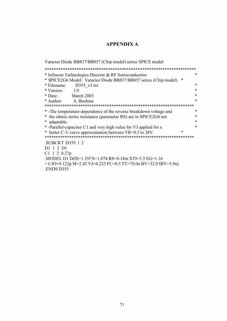
8/11/2019 2_template Fyp Final Report4
http://slidepdf.com/reader/full/2template-fyp-final-report4 70/75
APPENDI A
Caractor Diode **/HB**;H 4+hip model6 series S<I+E model
````````````````````````
` Infineon )echnologies Discrete K 7 Semiconductors `
` S<I+E10 $odel: Caractor Diode **/HB**;H series 4+hip model6 `
` ilename: D/;;[v/.t!t `
` Cersion: /. `
` Date: $arch / `
` Author: A. *oehme `
```````````````````````````````````````````````````````````````````
` 9)he temperature9dependence of the reverse breakdown voltage and `` the ohmic series resistance 4parameter 7S6 are in S<I+E10 not `
` adaptable. `
` 9<arallel9capacitor += and very high value for C5 applied for a `
` better +9C curve appro!imation between C7.; to C. `
```````````````````````````````````````````````````````````````````
.SF*+&) D/;; =
D= = D=
+= = .Hp
.$DE% D= D4IS=./;f =.H> 7S.=m L)I/.; E1=.=0
T +5J.=p $.> C50./ +.; ))H.n *C/. I*C;.u6
.EDS D/;;
H=
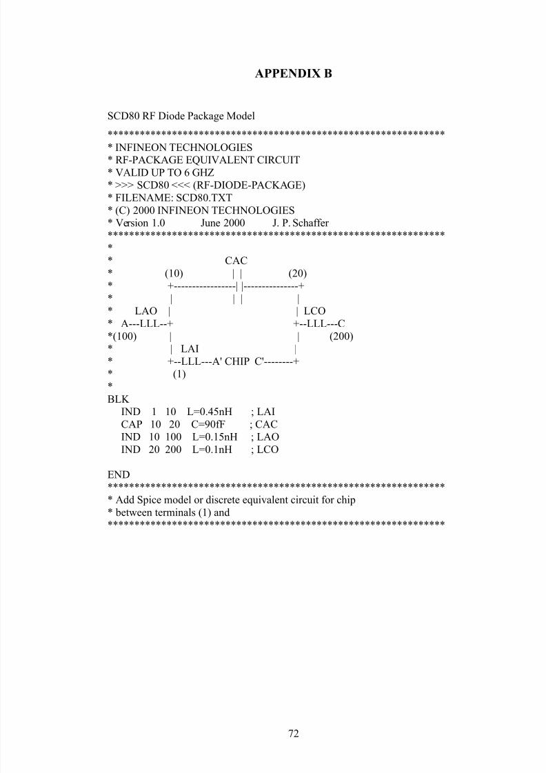
8/11/2019 2_template Fyp Final Report4
http://slidepdf.com/reader/full/2template-fyp-final-report4 71/75
APPENDI B
S+D 7 Diode <ackage $odel
```````````````````````````````````````````````````````````````` IIE )E+%1IES
` 79<A+&A1E E8FICA%E) +I7+FI)
` CA%ID F< ) 0 1\
` QQQ S+D PPP 479DIDE9<A+&A1E6
` I%EA$E: S+D.)L)
` 4+6 IIE )E+%1IES
` Cersion =. 5une 5. <. Schaffer
```````````````````````````````````````````````````````````````
`
` +A+
` 4=6 ] ] 46` T99999999999999999] ]999999999999999T
` ] ] ] ]
` %A ] ] %+
` A999%%%99T T99%%%999+
`4=6 ] ] 46
` ] %AI ]
` T99%%%999AU +I< +U99999999T
` 4=6
`
*%&
ID = = %.>;n # %AI
+A< = +Jf # +A+
ID = = %.=;n # %A
ID %.=n # %+
ED
```````````````````````````````````````````````````````````````
` Add Spice model or discrete e-uivalent circuit for chip
` between terminals 4=6 and
```````````````````````````````````````````````````````````````
H
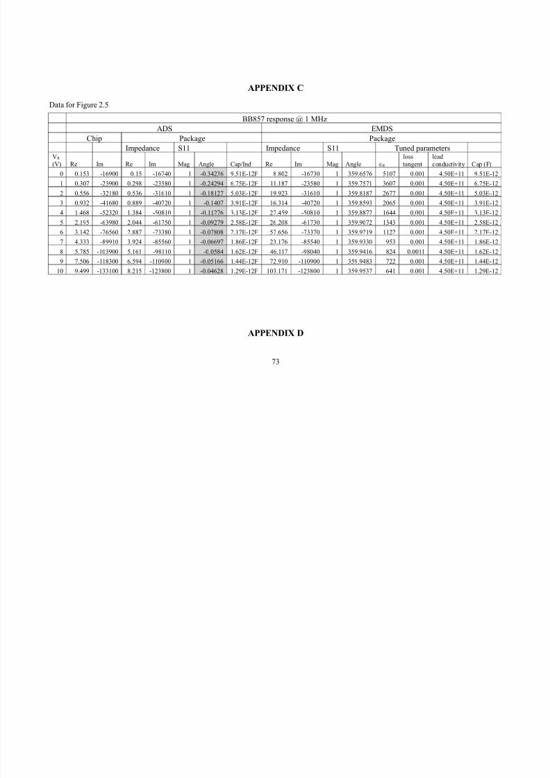
8/11/2019 2_template Fyp Final Report4
http://slidepdf.com/reader/full/2template-fyp-final-report4 72/75
APPENDI C
Data for igure .;
**;H response X = $2
ADS E$DS
+hip <ackage <ackage
Impedance S== Impedance S== )uned parametersC7
4C6 7e Im 7e Im $ag Angle +apBInd 7e Im $ag Angle 7
loss
tangent
lead
conductivity +ap 46
.=;/ 9=0J .=; 9=0H> = 9./>/0 J.;=E9= . 9=0H/ = /;J.0;H0 ;=H .= >.;ET== J.;=E9=
= ./H 9/J .J 9/; = 9.>J> 0.H;E9= ==.=H 9/; = /;J.H;H= /0H .= >.;ET== 0.H;E9=
.;;0 9/= .;/0 9/=0= = 9.==H ;./E9= =J.J/ 9/=0= = /;J.=H 0HH .= >.;ET== ;./E9=
/ .J/ 9>=0 .J 9>H = 9.=>H /.J=E9= =0./=> 9>H = /;J.;J/ 0; .= >.;ET== /.J=E9=
> =.>0 9;/ =./> 9;= = 9.==H0 /.=/E9= H.>;J 9;= = /;J.H =0>> .= >.;ET== /.=/E9=
; .=J; 90/J .>> 90=H; = 9.JHJ .;E9= 0. 90=H/ = /;J.JH =/>/ .= >.;ET== .;E9=
0 /.=> 9H0;0 .H 9H// = 9.H .=HE9= ;H.0;0 9H//H = /;J.J=J == .= >.;ET== .=HE9=
H >./// 9JJ= /.J> 9;;0 = 9.00JH =.0E9= /.=H0 9;;> = /;J.J// J;/ .= >.;ET== =.0E9=
;.H; 9=/J ;.=0= 9J== = 9.;> =.0E9= >0.==H 9J> = /;J.J>=0 > .== >.;ET== =.0E9=
J H.;0 9==/ 0.;J> 9==J = 9.;=00 =.>>E9= H.J= 9==J = /;J.J>/ H .= >.;ET== =.>>E9=
= J.>JJ 9=//= .=; 9=/ = 9.>0 =.JE9= =/.=H= 9=/ = /;J.J;/H 0>= .= >.;ET== =.JE9=
APPENDI D
H/
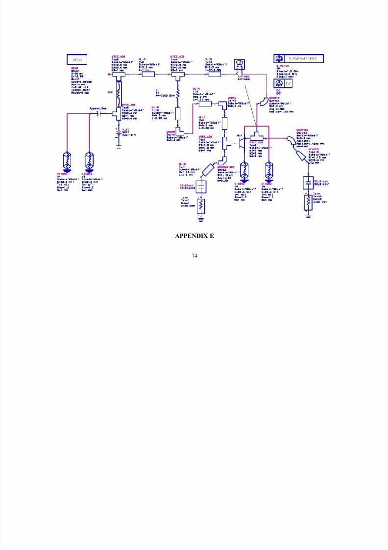
8/11/2019 2_template Fyp Final Report4
http://slidepdf.com/reader/full/2template-fyp-final-report4 73/75
MSub
DC
S-PARAMETERS
APPENDI E
H>
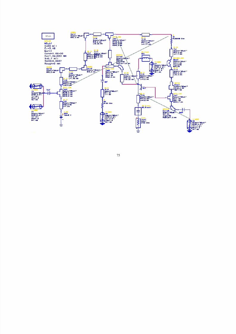
8/11/2019 2_template Fyp Final Report4
http://slidepdf.com/reader/full/2template-fyp-final-report4 74/75
MSub
H;

8/11/2019 2_template Fyp Final Report4
http://slidepdf.com/reader/full/2template-fyp-final-report4 75/75
LIST OF PUBLICATIONS
Amir Effendy $uhammad9Afifi, "idad Ismail and 5S $andeep. Vigh )uning
Sensitivity Dielectric 7esonator scillator from ptimi2ation of Dielectric
7esonator )E=δ 7esonant $ode +oupling.W $icrowave 5ournal, ori2on ouse<ublications Inc. 4in press6