Embed Size (px)
Citation preview

2D materials are an important emerging field of research due to their unique properties for applications in photovoltaics, semiconductors, battery technology and many other areas. 2D materials have been characterized by multiple nanoscale and microscopy techniques to gain a better understanding of the nature of their properties. Nanoscale FTIR techniques extend this characterization with critical chemical and optical data at the nanoscale.
The Anasys nanoIR3-s system provides two complementary nanoscale FTIR techniques for spectroscopy and near-field imaging, scattering-scanning near-field optical microscopy (s-SNOM) and photothermal AFM-Infrared (AFM-IR), including resonance-enhanced AFM-IR and Tapping AFM-IR. AFM-IR absorption spectra are direct measurements of sample absorption, independent of other complex optical properties of the tip and sample. As such, the spectra
Figure 1
Application Note #1512D Materials Characterization Using Nanoscale FTIR Spectroscopy and Near-field Imaging

Extending s-SNOM into Nanoscale FTIR Spectroscopy
Figures 1 and 2 illustrate the s-SNOM and photothermal AFM-IR techniques. Tapping AFM-IR is a recent advancement in AFM-IR that provides higher resolution chemical imaging and extends AFM-IR spectroscopy to a broader application range. Recent Bruker developments in s-SNOM technology have enabled the extension of this technique to nanoscale FTIR spectroscopy across the broadest available mid-IR range.
Figure 3 shows the modes of operation available with the nanoIR3-s Broadband laser. In a single source, the system provides 2 modes. The spectroscopy mode provides the largest spectral range for s-SNOM in a single laser source (670 cm-1 to >4000 cm-1), and the imaging mode provides the largest available imaging range (670 cm-1 to >2000 cm-1), eliminating the need to buy QCL lasers for imaging.
correlate very well to conventional bulk transmission IR. Scattering SNOM is a technique that investigates the optical and chemical properties of the material surface, and that providing correlation to reflection-based spectroscopy techniques. Atomic force microscopy (AFM) based techniques provide nanoscale information on the electrical, thermal, and mechanical properties of these materials.
Traditionally, 2D materials have been characterized with s-SNOM imaging techniques for optical and chemical information, but with the development of applications such as functionalization and nanopatterning, the AFM-IR can better provide unique information and valuable insights about materials, accelerating innovative research and capabilities.
Together, these complementary techniques provide new insights into the nanoscale chemical and complex optical properties of 2D materials with resolutions of 10 nm, orders of magnitude below the diffraction limit of conventional IR spectroscopy.
This application note describes using these complementary techniques for the characterization of a variety of 2D materials, including graphene, hexagonal boron nitride, nanoantennae and semiconductor materials.
Figure 2
Figure 3. nanoIR Broadband modes.

Complementary Nanoscale IR Techniques
The nanoIR3-s has the ability to acquire nanoscale images and IR spectra using two separate near-field spectroscopy techniques: photothermal AFM-IR and s-SNOM. These complementary techniques offer nanoscale chemical analysis, as well as optical, thermal, electrical, and mechanical mapping with spatial resolution down to a few nanometers for both soft and hard matter applications.
Nanoscale IR spectroscopy combines the precise chemical identification of infrared spectroscopy with the nanoscale capabilities of AFM to chemically identify sample components with a chemical spatial resolution down to 10 nm with monolayer sensitivity, breaking the diffraction limit by >100x. AFM-IR absorption spectra are direct measurements of sample absorption, independent of other complex optical properties of the tip and sample. As such, the spectra correlate very well to that of conventional bulk transmission IR.
Imaging of Plasmons and Phonons
Surface plasmon polaritons (SPPs) and surface phonon polaritons (SPhPs) in 2D materials, with their high spatial confinement, can open up new opportunities for enhanced light-matter interaction, super lenses, subwavelength metamaterial, and other novel photonic devices. In-situ characterization of these polaritonic excitations across different applications requires a versatile optical imaging and spectroscopy tool with nanometer spatial resolution. Through a non-invasive near-field light-matter interaction, s-SNOM provides a unique way to selectively excite and locally detect electronic and vibrational resonances in real space.
This technique is demonstrated by imaging the SPhPs of hexagonal boron nitride (hBN) as shown in Figure 4. Amplitude and phase near-field optical images provide complementary information for thorough characterization of the polaritonic resonances. Greater than 90° phase shift of SPhPs are observed on hBN, indicating strong light-matter coupling.
Similar to the visualization of SPhPs in hBN, the SPPs of graphene can also be investigated using the nanoIR3-s system. Figure 5 illustrates the standing wave of an SPP on a graphene wedge. Generally, the spatial resolution of s-SNOM is limited only by the end radius of the AFM probe, enabling the s-SNOM technique to measure cross sections of the SPP down to ~8 nm.
Figure 4. (a) AFM height image shows homogeneous hBN surface with different layers on a Si substrate; (b) s-SNOM amplitude shows strong interference fringes due to propagating SPhP along the surface on hBN; (c) s-SNOM phase shows a different phase signal with layer thickness; and (d) nano FTIR spectra of hBN.
A
B
C
D

Nanoscale Patterning of 2D Materials and Photothermal Effects
The controlled nanoscale patterning of 2D materials is a promising approach for engineering the optoelectronic, thermal, and mechanical properties of these materials to achieve novel functionalities and devices. Researchers at Harvard University undertook high-resolution patterning of hexagonal boron nitride (hBN).2 Through this nanofabrication approach various structures were created, including a 35 nm pitch grating and individual structure sizes down to 20 nm. Subsequent measurements by photothermal and scanning near-field optical microscopy measured the resulting near-field absorption and scattering of the nanostructures. These measurements revealed a large photothermal expansion of nanostructured hBN that is dependent on the height-to-width aspect ratio of the nanostructures. This effect is attributed to the large anisotropy of the thermal expansion coefficients of hBN and the nanostructuring implemented. The photothermal expansion should be present in other van der Waals materials with large anisotropy, and can lead to applications such as nanomechanical switches driven by light.
Functionalized 2D Materials Characterization with AFM-IR
Chemical functionalization of 2D materials is a key step in realizing their full potential in a wide range of applications. Nanoscale FTIR spectroscopy meets the growing need for unambiguous, non-destructive identification of chemical groups, as well as the mapping of their distribution on such materials with nanoscale spatial resolution and at monolayer thicknesses. Researchers at the National Graphene Center, University of Manchester have shown that photothermal AFM-IR can be used to analyze single-layer reduced graphene oxide flakes that have been non-covalently functionalized with sulfonated pyrenes.1 In their research, AFM-IR distinguished between the different pyrene moieties and mapping the sulfonate groups on a 1.7 nm functionalized monolayer of reduced graphene oxide with 32 nm spatial resolution, see Figure 6. AFM-IR is also shown to be sensitive to small changes in the sulfonate absorption spectra arising from chemical and surface effects. It was able to distinguish between different functionalizing molecules, even on materials with anisotropic thermal conductivity.
Figure 5. Imaging of surface plasmon polariton on a graphene wedge: (a) s-SNOM amplitude; (b) s-SNOM phase with a line cross section of the SPP standing wave; (c) s-SNOM phase line profile; and (d) cross section of a standing wave showing 10 nm resolution.
A B C D
Figure 6. (a) Single-flake AFM-IR spectra of i) PBSrGO, ii) PCNBS-rGO and, iii) U-rGO; and (b) average AFM-IR spectra of i) PBS-rGO, ii) PCNBS-rGO, and iii) U-rGO, dashed lines highlighting the 1084 and 1036 cm-1 intensities used for further chemical mapping studies.
A B
Figure 7: Photothermal infrared spectroscopy and imaging: (a) photothermal spectra taken from four different locations along the thinner region of the hBN grating, showing a strong SiO2 absorption peak at 1084 cm-1; (b) photothermal spectra taken from four different locations along the thicker region of the hBN grating, showing a strong and broad hBN absorption peak at 1368 cm-1; (c) AFM image of the top right corner of the hBN grating at 1368 cm-1; and (d) photothermal image of the same region at 1600 cm-1. No photothermal contrast was detected, indicating no absorption or mechanical expansion.
A
C
B
D
In addition to the ability to collect high-resolution images of optical phenomenon, the nanoIR3-s provides the capability to spectrally probe nanoscale surface features. Figure 10 shows the AFM-IR spectra collected on single rod and coupled antenna, and the antenna resonance can be clearly resolved at 910 cm-1, in agreement with theoretical predictions.
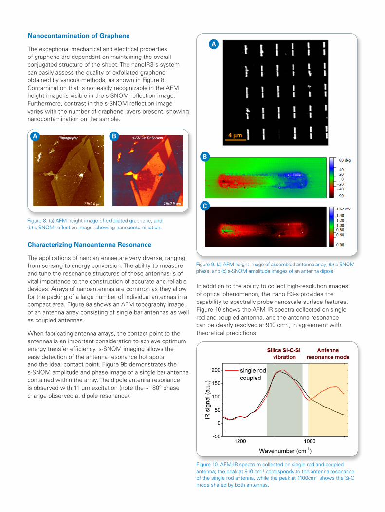
Nanocontamination of Graphene
The exceptional mechanical and electrical properties of graphene are dependent on maintaining the overall conjugated structure of the sheet. The nanoIR3-s system can easily assess the quality of exfoliated graphene obtained by various methods, as shown in Figure 8. Contamination that is not easily recognizable in the AFM height image is visible in the s-SNOM reflection image. Furthermore, contrast in the s-SNOM reflection image varies with the number of graphene layers present, showing nanocontamination on the sample.
Characterizing Nanoantenna Resonance
The applications of nanoantennae are very diverse, ranging from sensing to energy conversion. The ability to measure and tune the resonance structures of these antennas is of vital importance to the construction of accurate and reliable devices. Arrays of nanoantennas are common as they allow for the packing of a large number of individual antennas in a compact area. Figure 9a shows an AFM topography image of an antenna array consisting of single bar antennas as well as coupled antennas.
When fabricating antenna arrays, the contact point to the antennas is an important consideration to achieve optimum energy transfer efficiency. s-SNOM imaging allows the easy detection of the antenna resonance hot spots, and the ideal contact point. Figure 9b demonstrates the s-SNOM amplitude and phase image of a single bar antenna contained within the array. The dipole antenna resonance is observed with 11 µm excitation (note the ~180° phase change observed at dipole resonance).
Figure 10. AFM-IR spectrum collected on single rod and coupled antenna; the peak at 910 cm-1 corresponds to the antenna resonance of the single rod antenna, while the peak at 1100cm-1 shows the Si-O mode shared by both antennas.
Figure 8. (a) AFM height image of exfoliated graphene; and (b) s-SNOM reflection image, showing nanocontamination.
A B
Figure 9. (a) AFM height image of assembled antenna array; (b) s-SNOM phase; and (c) s-SNOM amplitude images of an antenna dipole.
A
B
C

Analysis of Carbon Nanotubes with Nanoscale IR
The AFM-IR technique functions by detecting the thermal expansion of a material, induced by the absorption of infrared illumination. The thermal expansion of a material is dependent on several factors, including the coefficient of thermal expansion and the thickness of the material. 1D and 2D materials, such as single-walled carbon nanotubes (CNT) and single-layer graphene have both a low coefficient of thermal expansion and also a thickness of roughly 1-2 nm. The nature of these 1D and 2D samples can make characterization challenging.
By placing a thin layer of polymeric material underneath graphene and CNT samples, a two orders of magnitude increase in AFM-IR signal intensity is observed.4, 5 As the thin sample absorbs the incident IR radiation, the heat generated is transferred to the thin polymer, which has a significantly higher coefficient of thermal expansion, and it expands. Figure 12 illustrates the finite element analysis model used to simulate the effects polymer thickness on the thermal expansion and temperature changes.
Characterizing the Effects of Polarized Light on Metasurface Chirality with s-SNOM and AFM-IR
For the first time, the combination of the complementary nanoscale imaging techniques, AFM-IR and s-SNOM have been used to investigate the role of chirality in the origins of circular dichroism in 2D nanoscale materials. Chiral molecules are a type of molecule that have a non-superimposable mirror image. These mirror images of chiral molecules are often called left handed and right handed, but due to the vector nature of light, they can be both left and right circularly polarized. Fully two-dimensional (2D) metamaterials, also known as metasurfaces, comprised of planar-chiral plasmonic metamolecules that are just nanometers thick, have been shown to exhibit chiral dichroism in transmission (CDT). Theoretical calculations indicate that this surprising effect relies on finite non-radiative (ohmic) losses of the metasurface. Until now this surprising theoretical prediction has never been experimentally verified because of the challenge of measuring non-radiative loss on the nanoscale.
Scattering SNOM was used to map the optical energy distribution when the structures were exposed to RCP and LCP IR radiation, while AFM-IR was used to detect the drastically different ohmic heating observed under RCP and LCP radiation.3
Through this study, it has been conclusively established for the first time that the circular dichroism observed in 2D metasurfaces can be attributed to handedness-dependent ohmic heating, as shown in Figure 11.
Figure 11. Experimentally measured AFM cantilever deflection amplitudes. The cantilever deflection is directly proportional to temperature increase in the sample during the laser pulse; this confirms that the magnitude and spatial distribution of the Ohmic heating of a chiral 2D metasurface markedly depends on the handedness of light.3
Figure 12. (a) Temperature rise (ΔT) and expansion (ΔZ) as a function of polymer thickness beneath the sample; temperature rise with no polymer (b) and with polymer (c) beneath the sample; vertical thermomechanical expansion with no polymer (d) and with polymer (e) beneath the sample.
A
B C
D E

The model was verified by examining an array of CNTs deposited on top of a layer of 150 nm thick polystyrene on a ZnSe prism. A region of the polymer substrate was removed prior to CNT deposition to ensure there was a region of CNT without polymer underneath. As can be seen in Figure 13, the IR chemical image collected at 4000 cm-1 shows clear signal from the CNT in the region that is supported by polystyrene, while no signal is observed where the polymer substrate has been removed. It has been suggested that the varying AFM-IR signal from different CNTs is caused by the difference between metallic and semiconducting tubes.
Figure 13c shows the AFM-IR imaging of graphene on top of a 106 nm thick layer of PMMA. This image shows the extension of this technique to monolayer 2D materials. The amplification of the AFM-IR signal by a thin layer of polymer increases the signal intensity by two orders of magnitude. This new technique allows for AFM-IR characterization of 1 nm thick 1D and 2D materials that was previously impossible. Going forward, this dramatic signal enhancement may be applied to a variety of applications, including ultrathin biologicals and a variety of 1D and 2D materials.
Investigating Exothermic Peaks of Polyethylene Using nanoTA and LCR
Polyethylene (PE) is one of the most widely utilized polymers, with uses in numerous industries, including 2D materials applications. To change the mechanical, thermal, and electrical properties of PE, inorganic fillers, such as graphite and metallic particles, have been added. In recent years, hBN has shown promise as a filler due to its high mechanical strength, thermal conductivity, and insulating properties. Researchers at Sichuan University used nanothermal analysis (nanoTA) and Lorentz contact resonance (LCR) to characterize this effect of hBN particles on the melting behavior of PE.5
LCR imaging is able to clearly show regions of high hBN concentration on the surface, as shown in Figure 14a and b. Then nanoTA was used to measure the softening temperature of various regions of the material. There was an increase shown in the transition temperature of 4-8°C for areas of the PE sample near hBN aggregates when compared to areas without hBN, as shown in Figure 14. The accuracy of this technique was verified when compared to traditional DSC analysis, with the bulk transition temperature within the standard deviation of nanoTA values (see Figure 14d). These results, combined with DSC analysis, show that the meso-phase of the PE forms near hBN particles during crystallization, which induces a weak exothermic peak that was previously unexplained. Figure 14 also illustrates nanoTA measurement performed directly on the hBN particles, for which no thermal transition was measured at temperatures up to 400°C.
Figure 13. (a) AFM topography imaging of CNTs deposited on a polystyrene substrate; (b) IR chemical mapping at 4000 cm-1 showing absorption by CNTs; and (c) IR chemical mapping image of monolayer graphene captured at 4000 cm-1.
A B C
Figure 14. (a) LCR-AFM height image; (b) AFM mechanical image (using LCR) of the PE/BN composites, showing boron nitride clusters in the areas A,D and E; (c) local thermal analysis data of the assigned positions were obtained by nanoTA, comparing the melting temperatures of PE and BN; and (d) DSC from the PE/BN composites (heating rate of 2°C min-1).
A
C
B
D

Analyzing Thermal Conductivity of Graphene Sheets with SThM
Graphene has been a focus of recent research due to its high thermal conductivity and potential in optoelectronics. Scanning thermal microscopy (SThM) characterizes thermal conductivity of 2D materials, as it yields high sensitivity in resistance detection between the probe and the sample. These high spatial resolutions remove ambiguity in the detection of the source of a sample’s electrical capabilities, making SThM a reliable method of monitoring a sample temperature, as well as its thermal conductivity.
Researchers at Lancaster University and Durham University used SThM to investigate thermal conductivity on single and multilayer graphene sheets.6 Graphene was deposited on an Si/SiO2 substrate with prepatterned trenches, with both graphene suspended over the trench and supported by the substrate imaged. It was found that increasing the number of supported graphene layers led to a clear decrease in thermal resistance. A key observation was that the thermal conductance of both bilayer and multilayer graphene suspended over the trench was greater than that of the supported layer. This finding is contrary to expectations that conduction from the graphene to the substrate would produce greater heat dissipation. As the mean free path of thermal phonons in graphene is much greater than the height of the trench, it is hypothesized that ballistic acoustic phonons from the SThM tip are the main source of heat transfer, with 90% reaching the trench in the ballistic regime. A graphene bulge that was still suspended over the trench exhibited similar properties, ruling out experimental differences, such as SThM contact area, as the reason for such behavior.
These measurements concluded that three-layer graphene had approximately 68% of the thermal conductance when compared to single-layer graphene. Finally, thermal mapping of border regions between supported graphene layers shows that the thermal transition region has a width of 50-100 nm, verifying theoretical estimates for the mean free path.
Figure 15. (a) SThM image of supported graphene, showing varied thicknesses throughout the sample; and (b) measured contact thermal resistance as a function of the number of graphene layers, showing reduction in thermal resistance as the number of layers increases.
A
B

Bruker Nano Surfaces DivisonSanta Barbara, CA · USAphone [email protected]
©20
19 B
ruke
r C
orpo
ratio
n. A
nasy
s, n
anoI
R3
-s, a
nd n
anoI
R3
-s B
road
band
are
tra
dem
arks
of
Bru
ker
Cor
pora
tion.
All
othe
r tr
adem
arks
are
the
pro
pert
y of
the
ir re
spec
tive
com
pani
es. A
ll rig
hts
rese
rved
. AN
151,
Rev
. B0.
www.bruker.com/nanoIR
Conclusions
Traditionally, 2D materials have been characterized with s-SNOM imaging techniques for optical characterization and chemical analysis. 2D materials characterization continues to evolve with the development of such applications as functionalization and nanopatterning, and the understanding of a more complete set of material properties, including radiative and absorptive material properties.
Recent developments in near-field spectroscopy, such as s-SNOM-based nanoscale FTIR spectroscopy and the use of resonance-enhanced and Tapping AFM-IR techniques, have extended the characterization capabilities for this class of materials to provide unique and complementary information, accelerating learning and new discoveries. The nanoIR3-s Broadband instrumentation helps enable these advances and provides the most comprehensive set of capabilities available for 2D materials characterization.
References
1. Bartlam C et al., "Nanoscale infrared identification and mapping of chemical functional groups on graphene," Carbon 139 (2018): 317-24.
2. Loepz et al., "Large photothermal effect in sub-40 nm h-BN nanostructures patterned via high resolution ion beam," DOI: 10.1002/smll.201800072.
3. Khanikaev AB, Arju N, Fan Z, Purtseladze D, Lu F, Lee J, Sarriugarte P, Schnell M, Hillenbrand R, Belkin MA, and Shvets G., "Experimental demonstration of the microscopic origin of circular dichroism in two-dimensional metamaterials," Nature Communications (2017).
4. Rosenberger MR, Wang MC, Xie X, Rogers JA, N S, and K WP, "Measuring individual carbon nanotubes and single graphene sheets using atomic force microscope infrared spectroscopy," Nanotechnology (2017).
5. Zhang X, Wu H, Guo S, and Wang Y, "Understanding in crystallization of polyethylene: the role of boron nitride (BN) particles," Royal Social of Chemistry Advances 121 (2015): 99585-100407.
6. Pumarol ME, Rosamond MC, Tovee P, Petty MC, Zeze DA, Falko V, and Kolosov OV, "Direct Nanoscale Imaging of Ballistic and Diffusive Thermal Transport in Graphene Nanostructures," Nano Letters 12 (2012): 2906-2911.


![Exploring Nanomechanical Properties of Materials with ... · perform high-resolution imaging of surfaces for a broad range of materials [1]. Initially, this function was realized](https://img.dokumen.tips/doc/110x75/60d1bfef0b03003bf0775237/exploring-nanomechanical-properties-of-materials-with-perform-high-resolution.jpg)