Embed Size (px)
Citation preview
2D Digital Filter Implementation ona FPGA
by
Danny T. Tsuei
A thesispresented to the University of Waterloo
in fulfillment of thethesis requirement for the degree of
Master of Applied Sciencein
Electrical and Computer Engineering
Waterloo, Ontario, Canada, 2011
c© Danny T. Tsuei 2011

I hereby declare that I am the sole author of this thesis. This is a true copy of the thesis,including any required final revisions, as accepted by my examiners.
I understand that my thesis may be made electronically available to the public.
Danny T. Tsuei
ii

Abstract
The use of two dimensional (2D) digital filters for real-time 2D data processing hasfound important practical applications in many areas, such as aerial surveillance, satelliteimaging and pattern recognition. In the case of military operations, real-time image pro-cessing is extensively used in target acquisition and tracking, automatic target recognitionand identification, and guidance of autonomous robots. Furthermore, equal opportuni-ties exist in civil industries such as vacuum cleaner path recognition and mapping andcar collision detection and avoidance. Many of these applications require dedicated hard-ware for signal processing. It is not efficient to implement 2D digital filters using a singleprocessor for real-time applications due to the large amount of data. A multiprocessorimplementation can be used in order to reduce processing time.
Previous work explored several realizations of 2D denominator separable digital filterswith minimal throughput delay by utilizing parallel processors. It was shown that regard-less of the order of the filter, a throughput delay of one adder and one multiplier can beachieved. The proposed realizations have high regularity due to the nature of the proces-sors. In this thesis, all four realizations are implemented in a Field Programming GateArray (FPGA) with floating point adders, multipliers and shift registers. The implementa-tion details and design trade-offs are discussed. Simulation results in terms of performance,area and power are compared.
From the experimental results, realization four is the ideal candidate for implementationon an Application Specific Integrated Circuit (ASIC) since it has the best performance,dissipates the lowest power, and uses the least amount of logic when compared to otherrealizations of the same filter size. For a filter size of 5 × 5, realization four can producea throughput of 16.3 million pixels per second, which is comparable to realization one andabout 34% increase in performance compared to realization one and two. For the givenfilter size, realization four dissipates the same amount of dynamic power as realization one,and roughly 54% less than realization three and 140% less than realization two. Further-more, area reduction can be applied by converting floating point algorithms to fixed pointalgorithms. Alternatively, the denormalization and normalization stage of the floatingpoint pipeline can be eliminated and fused together in order to save hardware resources.
iii

Acknowledgments
I would like to give thanks to my supervising professors, Professor Mohamed YahiaDabbagh and Professor Manoj Sachdev for their dedication, encouragement, and guidanceduring my graduate studies here at the University of Waterloo. I would like to thank themfor reading and critiquing this thesis. I would also like to thank my thesis readers, ProfessorBill Bishop and Professor Sebastian Fischmeister for their feedbacks and corrections onvarious parts of this thesis.
I would like to show my appreciation to the administrative staff in the Electrical andComputer Engineering department, Wendy Boles, Wendy Stoneman, Irena Baltaduonis,Susan King, and Annette Dietrich, for their assistance with the necessary paper work tofulfill my graduation requirement. Also, I would like to express my thanks to Philip Regierand Paul Ludwig for their technical assistance with regard to computer hardware.
To the members of CMOS Design and Reliability (CDR) group, David Li, PierceChuang, Jaspal Shah, Tasreen Charania and others, I couldn’t have made it through grad-uate studies without your help. Thank you all for the constant encouragement throughgood times and bad. It was a pleasure to have you all by my side.
Lastly, I would like to express my gratitude to my parents, who supported me bothfinancially and mentally, and for that I am grateful. I hope I have made you proud and Ican continue to do so in the future.
iv

Dedication
This thesis is dedicated to
My parents, Edward and Ginafor their unconditional love and support
v

Table of Contents
List of Tables ix
List of Figures xi
1 Introduction 1
1.1 Research Contribution . . . . . . . . . . . . . . . . . . . . . . . . . . . . . 2
1.2 Thesis Overview . . . . . . . . . . . . . . . . . . . . . . . . . . . . . . . . . 3
2 Realization of 2D Separable Denominator Digital Filters 4
2.1 General Form . . . . . . . . . . . . . . . . . . . . . . . . . . . . . . . . . . 4
2.2 Realization One . . . . . . . . . . . . . . . . . . . . . . . . . . . . . . . . . 5
2.3 Realization Two . . . . . . . . . . . . . . . . . . . . . . . . . . . . . . . . . 7
2.4 Realization Three . . . . . . . . . . . . . . . . . . . . . . . . . . . . . . . . 11
2.5 Realization Four . . . . . . . . . . . . . . . . . . . . . . . . . . . . . . . . 14
3 Filter Coefficients Derivation 17
3.1 Realization One . . . . . . . . . . . . . . . . . . . . . . . . . . . . . . . . . 20
3.2 Realization Two . . . . . . . . . . . . . . . . . . . . . . . . . . . . . . . . . 21
3.3 Realization Three . . . . . . . . . . . . . . . . . . . . . . . . . . . . . . . . 24
3.3.1 Modification to Realization Three . . . . . . . . . . . . . . . . . . . 30
3.4 Realization Four . . . . . . . . . . . . . . . . . . . . . . . . . . . . . . . . 31
vi

4 Timing Considerations on Filter Implementation 33
4.1 Critical Data Path in Realization One . . . . . . . . . . . . . . . . . . . . 33
4.2 Critical Data Path in Realization Two . . . . . . . . . . . . . . . . . . . . 36
4.3 Critical Data Path in Realization Three and Four . . . . . . . . . . . . . . 38
4.4 Control Path . . . . . . . . . . . . . . . . . . . . . . . . . . . . . . . . . . 40
5 System Implementation Details 43
5.1 Fixed Point versus Floating Point . . . . . . . . . . . . . . . . . . . . . . . 45
5.2 Multiplier and Adder Pipeline Depth . . . . . . . . . . . . . . . . . . . . . 47
5.3 Shift Registers . . . . . . . . . . . . . . . . . . . . . . . . . . . . . . . . . . 48
5.4 Implementation of a DSP System . . . . . . . . . . . . . . . . . . . . . . . 49
5.4.1 Communication Protocol to the FPGA . . . . . . . . . . . . . . . . 49
5.4.2 DSP System Architecture . . . . . . . . . . . . . . . . . . . . . . . 50
6 Simulation Results 56
6.1 Functional Correctness . . . . . . . . . . . . . . . . . . . . . . . . . . . . . 56
6.2 Filters of Varying Sizes . . . . . . . . . . . . . . . . . . . . . . . . . . . . . 60
6.2.1 Performance . . . . . . . . . . . . . . . . . . . . . . . . . . . . . . . 60
6.2.2 Logic Utilization . . . . . . . . . . . . . . . . . . . . . . . . . . . . 62
6.2.3 Power Dissipation . . . . . . . . . . . . . . . . . . . . . . . . . . . . 65
7 Conclusions and Future Work 67
7.1 Conclusions . . . . . . . . . . . . . . . . . . . . . . . . . . . . . . . . . . . 67
7.2 Future Work . . . . . . . . . . . . . . . . . . . . . . . . . . . . . . . . . . . 68
References 68
APPENDICES 72
vii

A Detailed filter implementation on FPGA 73
A.1 Realization One . . . . . . . . . . . . . . . . . . . . . . . . . . . . . . . . . 73
A.2 Realization Two . . . . . . . . . . . . . . . . . . . . . . . . . . . . . . . . . 75
A.3 Realization Three . . . . . . . . . . . . . . . . . . . . . . . . . . . . . . . . 75
A.4 Realization Four . . . . . . . . . . . . . . . . . . . . . . . . . . . . . . . . 78
B Synthesizer and Fitter Settings for Performance Optimization 80
B.1 Synthesizer Settings . . . . . . . . . . . . . . . . . . . . . . . . . . . . . . . 80
B.2 Fitter Settings . . . . . . . . . . . . . . . . . . . . . . . . . . . . . . . . . . 80
viii

List of Tables
4.1 Cycle Time for Each Realization. . . . . . . . . . . . . . . . . . . . . . . . 42
5.1 IEEE 745 Single and Double Precision Floating Point Internal Representation 46
5.2 Hardware Utilization for FP Multiplier and FP Adder. . . . . . . . . . . . 48
5.3 Hardware Utilization for Horizontal and Vertical Shift Register. . . . . . . 49
6.1 Maximum Operating Speed (MHz) for Realization One With and WithoutDSE Optimization. . . . . . . . . . . . . . . . . . . . . . . . . . . . . . . . 60
6.2 Maximum Operating Speed (MHz) for Realization One, Two, Three andFour after Design Space Explorer. . . . . . . . . . . . . . . . . . . . . . . . 61
6.3 Theoretical and Actual Cycle Time for Each Realization . . . . . . . . . . 61
6.4 Throughput (million pixels/second) for Each Realization. . . . . . . . . . . 62
6.5 Processors Required for Each Realization (does not include the final treeadder). . . . . . . . . . . . . . . . . . . . . . . . . . . . . . . . . . . . . . . 62
6.6 Logic Utilization Required for Each Megawizard Library Module. . . . . . 63
6.7 Expected versus Actual Logic Utilization for Realization One. . . . . . . . 63
6.8 Actual Logic Utilization for Each Realization. . . . . . . . . . . . . . . . . 64
6.9 Power Dissipation for each Realization in mW. . . . . . . . . . . . . . . . . 66
ix
List of Figures
2.1 Realization One . . . . . . . . . . . . . . . . . . . . . . . . . . . . . . . . . 6
2.2 Realization Two: A Hybrid Parallel-Cascade Realization. . . . . . . . . . . 9
2.3 Realization Two. . . . . . . . . . . . . . . . . . . . . . . . . . . . . . . . . 10
2.4 Realization Three . . . . . . . . . . . . . . . . . . . . . . . . . . . . . . . . 12
2.5 Realization Three Implementation . . . . . . . . . . . . . . . . . . . . . . . 13
2.6 Realization Four. . . . . . . . . . . . . . . . . . . . . . . . . . . . . . . . . 15
3.1 Implementation for the Numerator and the Denominator for Equation 3.34. 31
4.1 Critical Paths in First, Second and Third Subfilter of Realization One. . . 34
4.2 Critical Path and Modified Critical Path for Realization One. . . . . . . . 35
4.3 Critical Paths in First, Second and Third Stages of Realization Two. . . . 36
4.4 Critical Path and Modified Critical Path for Realization Two. . . . . . . . 37
4.5 Denominator Realization for Realization Three and Four. . . . . . . . . . . 38
4.6 Numerator Realization . . . . . . . . . . . . . . . . . . . . . . . . . . . . . 39
4.7 Example Timing Diagrams Without Control Paths. . . . . . . . . . . . . . 40
4.8 Timing Diagram with Control Path. . . . . . . . . . . . . . . . . . . . . . . 42
5.1 FPGA versus ASIC Design Flow . . . . . . . . . . . . . . . . . . . . . . . . 44
5.2 FP Multiplier fmax and Register Count versus Pipeline Depth . . . . . . . 48
5.3 FP Adder fmax and Register Count versus Pipeline Depth . . . . . . . . . 48
5.4 DSP System Architecture . . . . . . . . . . . . . . . . . . . . . . . . . . . 51
x

5.5 Avalon MM Interface Between the JTAG to Avalon MM Interface and theFilter Coefficient . . . . . . . . . . . . . . . . . . . . . . . . . . . . . . . . 54
5.6 Avalon ST Interface Between the Avalon ST JTAG Interface and the DigitalFilter . . . . . . . . . . . . . . . . . . . . . . . . . . . . . . . . . . . . . . . 55
6.1 Original Sample Image . . . . . . . . . . . . . . . . . . . . . . . . . . . . . 57
6.2 Processed Sample Image . . . . . . . . . . . . . . . . . . . . . . . . . . . . 59
A.1 Realization One . . . . . . . . . . . . . . . . . . . . . . . . . . . . . . . . . 74
A.2 Realization Two . . . . . . . . . . . . . . . . . . . . . . . . . . . . . . . . . 75
A.3 Realization Three Subfilter One . . . . . . . . . . . . . . . . . . . . . . . . 76
A.4 Realization Three Subfilter Two . . . . . . . . . . . . . . . . . . . . . . . . 76
A.5 Realization Three Subfilter Three . . . . . . . . . . . . . . . . . . . . . . . 76
A.6 Realization Three Subfilter Four . . . . . . . . . . . . . . . . . . . . . . . . 76
A.7 Realization Three Subfilter Five . . . . . . . . . . . . . . . . . . . . . . . . 76
A.8 Realization Three Subfilter Six . . . . . . . . . . . . . . . . . . . . . . . . . 76
A.9 Realization Three Subfilter Seven . . . . . . . . . . . . . . . . . . . . . . . 77
A.10 Realization Three Subfilter Eight . . . . . . . . . . . . . . . . . . . . . . . 77
A.11 Realization Three Subfilter Nine . . . . . . . . . . . . . . . . . . . . . . . . 77
A.12 Realization Four z1 Roots . . . . . . . . . . . . . . . . . . . . . . . . . . . 78
A.13 Realization Four z2 Roots . . . . . . . . . . . . . . . . . . . . . . . . . . . 78
A.14 Realization Four Numerator Coefficients P, J, K, and L . . . . . . . . . . . 79
A.15 Realization Four Numerator Coefficients M, E, H and I . . . . . . . . . . . 79
A.16 Realization Four Numerator Coefficients B, D, G and O . . . . . . . . . . . 79
A.17 Realization Four Numerator Coefficients A, C, F, and N . . . . . . . . . . 79
xi
Chapter 1
Introduction
The application of Digital Signal Processing (DSP) algorithms impacts many aspects ofour contemporary standard of living [1].Much of our technological advancements in modernwireless and wired communications, medical imaging equipment, audio and visual productsare driven by new and emerging DSP algorithms [2, 3]. The advent of more complex DSPalgorithms with smaller and faster Integrated Circuits (ICs) contribute to the eventualityof complex systems. DSP algorithms typically, but not always, process real time data asthe data is acquired. This implies that DSP algorithms must produce a deterministic runtime to satisfy system-wide timing constraints.
A 2D digital filter is a type of DSP algorithm used to process 2D data and has foundimportant practical applications in many areas, including aerial surveillance, satellite imag-ing, pattern recognition, target acquisition and tracking [1, 2, 4, 5].
Traditionally DSP algorithms are implemented using digital signal processors that ex-ecute a set of instructions on a set of given input data. Special mathematical circuitryis often found on digital signal processors in order to facilitate complex mathematicalfunctions. Designers are required to write in a low level language in order to produce op-timized instructions for digital signal processors. However, in recent years, DSP designershave been shifting toward the use of Field Programming Gate Arrays (FPGA) for hard-ware development. Majority of the controversy between the digital signal processor versusFPGA surrounds the issue of processing capability, as measured in millions of instructionsper second (MIPS) [6, 7]. Other inherent advantages of the FPGA, including reliabilityand maintainability, are often ignored.
Since a digital signal processor is a special microprocessor that requires a stream ofinstructions to execute, not all the instructions are data related. Some instructions are
1

control related, some are protocol related, while some are DSP related. Resources in thedigital signal processor, such as internal registers, external memory, Direct Memory Access(DMA) controller, transfer buses and external input/output (I/O) signals are shared by allinstructions. This can cause unexpected behavior as one instruction attempts to modify theresults of another instruction. DSP algorithms are often required to run in real-time andany unexpected delays can result in system failure. FPGAs inherently negate this problemby issuing dedicated resources to the executing instructions. Dedicated data and controlpaths are placed and assigned to predetermined locations on the FPGA to ensure thefunctionality correctness while meeting timing constraints. Memory blocks are distributedthroughout the FPGA and each instruction is allocated the proper amount of memory forits execution. I/O signals are clearly defined from modules to modules, and eliminatesunexpected interactions between instructions. This also allows the designer to more easilylocate and isolate bugs [8]. Not only does FPGA guarantee dedicated run-time resources,verification is much more simplified on the FPGA than digital signal processors.
Operating system (OS) , or more commonly called kernels, is used to control resourcesharing on the digital signal processor. Allowable execution time, memory allocation andperipheral I/O access time are all managed by the operating system. However, there isan inherent conflict of interest between instruction efficiency and operating system inter-vention. For the instruction to work at optimal efficiency, it would be ideal to have zerointervention from the operating system. Compounding these difficulties is the lack of abil-ity to verify functional correctness. It is impossible to ensure all possible permutationsof the instructions plus OS interventions are tested during verification based on the largenumber of test cases. Challenges arises from complete functional verification is equallydaunting on FPGAs. However, at the fundamental level, much of the design and verifica-tion tools are shared between FPGA and its Application Specific Integrated Circuit (ASIC)counterpart. The FPGA designers are able to benefit from this mutual relationship sinceASIC designers are extremely intolerant of design bugs. It would take millions of dollarsin fabrication cost to fix an implementation error [8]. From these arguments, it is clearthat FPGA is an excellent hardware development platform for DSP designers.
1.1 Research Contribution
In this thesis, multiple implementations of two dimensional (2D) digital filters are pre-sented. The implementations are designed and optimized using Altera’s proprietary Quar-tus II software and simulated using ModelSim. Results in this thesis show that with minormodifications on the filter realization, the same throughput as derived from previous work
2

can be obtained.
A framework for future 2D filter implementations is also presented in this thesis. The2D digital filters are implemented as custom hardware blocks in the Altera System onProgrammable Chip (SOPC) Builder. This provides flexibility in customizing the DSPsystem using additional SOPC components, such as Nios II processor, Phase Locked Loops(PLLs), external Random Access Memory (RAM), and parallel I/Os that can be easilyintegrated into the design to tailor to different applications.
Several optimization techniques pertaining to Hardware Register Transfer level (RTL)are also discussed in the thesis. These techniques include selecting floating point (FP)operators, secondary clock divider circuit, specifying synopsis design constraint (SDC)file constraint for timing oriented fitting and using the Design Space Explorer (DSE) fortiming optimization. Future work carried out in the implementation of 2D digital filterson FPGA will benefit from these optimization techniques as they are transferable acrossdifferent RTL lanaguges and hardware platforms.
1.2 Thesis Overview
The remainder of this thesis is organized as follows. Chapter 2 presents the general form offour different 2D denominator separable digital filters. Chapter 3 discusses the derivationof filter coefficients from a sample impulse function as well as any architectural changes dueto complex poles. Chapter 4 discusses architectural changes related to these realizationsbased on timing considerations. Chapter 5 describes how the digital filter fits into thesystem from a top level perspective. Chapter 6 shows and analyzes the simulation results.Finally, chapter 7 concludes the thesis.
3
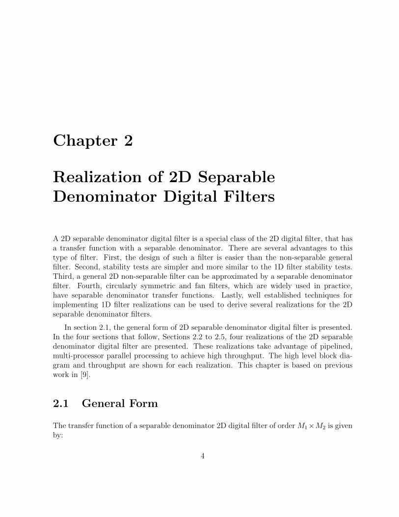
Chapter 2
Realization of 2D SeparableDenominator Digital Filters
A 2D separable denominator digital filter is a special class of the 2D digital filter, that hasa transfer function with a separable denominator. There are several advantages to thistype of filter. First, the design of such a filter is easier than the non-separable generalfilter. Second, stability tests are simpler and more similar to the 1D filter stability tests.Third, a general 2D non-separable filter can be approximated by a separable denominatorfilter. Fourth, circularly symmetric and fan filters, which are widely used in practice,have separable denominator transfer functions. Lastly, well established techniques forimplementing 1D filter realizations can be used to derive several realizations for the 2Dseparable denominator filters.
In section 2.1, the general form of 2D separable denominator digital filter is presented.In the four sections that follow, Sections 2.2 to 2.5, four realizations of the 2D separabledenominator digital filter are presented. These realizations take advantage of pipelined,multi-processor parallel processing to achieve high throughput. The high level block dia-gram and throughput are shown for each realization. This chapter is based on previouswork in [9].
2.1 General Form
The transfer function of a separable denominator 2D digital filter of order M1×M2 is givenby:
4

H(z1, z2) =G(z1, z2)
F (z1, z2)
=
∑M1
i=0
∑M2
j=0 bi,jz−i1 z
−j2∑M1
i=0 αiz−i1
∑M2
j=0 βjz−j2
=p(z1, z2)
q1(z1)q2(z2)
(2.1)
where F (z1, z2) and G(z1, z2) are the 2D Z-transforms of the input f(n1, n2) and the outputg(n1, n2). bi,j, αi and βj are constant coefficients that determine the characteristics of thefilter. The polynomials p(z1, z2), q1(z1) and q2(z2) are functions of the horizontal delay(z−1
1 ) and the vertical delay (z−12 ). M1 is the horizontal dimension and M2 is the vertical
dimension of the 2D digital filter. Also, we assume that the numerator and denomiatorare coprime and α0 = β0 = 1.
2.2 Realization One
The transfer function H(z1, z2) in (2.1) can be rewritten as a product of two subfilters:
H(z1, z2) = H1(z1)H2(z1, z2) (2.2)
where
H1(z1) =1
q1(z1)=
1∑M1
i=0 αiz−i1
(2.3)
H2(z1, z2) =p(z1, z2)
q2(z2)=
∑M1
i=0
∑M2
j=0 bi,jz−i1 z
−j2∑M2
j=0 βjz−j2
(2.4)
Equation (2.2) suggests the realization of H(z1, z2) as a cascade of two subfilters. Thefirst subfilter H1(z1) in (2.3) is an one dimensional (1D) Infinite Impulse Response (IIR)filter. This filter can be realized using the transposed direct form II, which is suitable fora multiprocessor implementation. The transfer function of the subfilter H2(z1, z2) can berewritten as:
5

H2(z1, z2) =
∑M2
j=0 bj(z1)z−j2∑M2
j=0 βjz−j2
(2.5)
where
bj(z1) =
M1∑i=0
bi,jz−i1 , j = 0, 1, ...,M2 (2.6)
Again, 1D realization structures can be used for the realization of this transfer function.The transposed direct form II structure is used to realize the subfilter, where in Equation2.5, bj(z1), j = 0, 1, ...M2 represents a set of 1D FIR filters.
1-1
1-1
1-1
1-1
1-1
1-1
1-1
1-1
2-1
2-1
2-1
w(n1,n2)f(n1,n2)
g(n1,n2)
xh1(n1,n2)
-α1
-αM1
xhM1(n1,n2)
-βM2
bM1,0 b0,0bM1-1,0
-β1
bM1,1 b0,2bM1-1,1
bM1,M2 b0,M2bM1-1,M2
uM2(n1,n2)
u0(n1,n2)
u1(n1,n2)
Figure 2.1: Realization One
Assuming the input is f(n1, n2), output is g(n1, n2), while w(n1, n2) and uj(n1, n2)(where j = 0...M2) are the intermediate state variables, the overall separable denominatorfilter has a completely decomposed realization as shown in Figure 2.1. The decomposed
6

realization consists of a cascade of three subfilters: a 1D horizontal IIR filter, a bank of1D horizontal FIR filters, and a 1D vertical IIR filter. It can be seen that this realizationhas the minimum number of vertical shifts, namely z−1
2 . A minimum number of verticalshifts is a desired feature since the physical implementation of a vertical shift is far moreexpensive in terms of hardware compared to a horizontal shift. For example, in a rasterscan image, a horizontal shift corresponds to a storage of one pixel of data, while a verticalshift corresponds to storage of an entire row of pixels. Since an FPGA is limited in termsof storage elements, be it RAM or registers, the less number of vertical shifts there are,the more likely the design will fit on the FPGA.
Pipelining and parallelism can be exploited effectively in the implementation of thedecomposed realization in Figure 2.1. Since each subfilter consists of multiple repeatinginstances of multipliers, adders and shift registers, a module can be created to include onemultiplier, one adder and one shift register. Cascading the module in parallel or series willproduce the desired filter. Modules can also be called processors. The temporary datastored in the shift registers can also be called states.
The first subfilter has M1 horizontal states and single intermediate output w(n1, n2).The states and the intermediate output have a computation structure that requires onemultiplication and two additions using M1 processors. The second subfilter has M1(M2+1)horizontal states and (M2 + 1) intermediate outputs. These states and the intermediateoutputs can be computed in a single multiplication and a single addition using (M1 +1)(M2 + 1) processors. The third subfilter has M2 vertical states and a single outputg(n1, n2). The computation of these states require the use of a processor that is composed oftwo adders, one multiplier and one shift register, assuming the first and the second subfiltersare processing in parallel with the third subfilter. The required number of processors (P )and the cycle time (T ) required for the realization are:
P = (M1 + 1)(M2 + 1) +M1 +M2 (2.7)
T = tmult + 2tadd + 1 (2.8)
2.3 Realization Two
The second realization is based on the decomposition of the numerator polynomial ofthe transfer function in Equation (2.1) by the general decomposition theorem [10]. This
7

theorem decomposes the 2D polynomial as a sum of products of simple 1D polynomials.The numerator of the transfer function H(z1, z2) in Equation (2.1) can be rewritten as
p(z1, z2) =
M1∑i=0
M2∑j=0
bi,jz−i1 z
−j2 = ZT
1 BZ2 (2.9)
where
ZT1 = [1, z−1
1 , z−21 , ..., z−M1
1 ] (2.10)
Z2 = [1, z−12 , z−2
2 , ..., z−M22 ] (2.11)
B = [bi,j] (2.12)
B is a matrix of dimension (M1 +1)× (M2 +1). There are many decompositions for thematrix B. In particular, it can always be decomposed as a product of two matrices. Themost commonly used decompositions in the literature are Singular Value Decomposition(SVD) [11], the Jordan Decomposition (JD) [12], and the Lower-Upper Decomposition(LUD) [13]. By decomposing the matrix B into a product of two matrices, multiplying,then expanding gives:
p(z1, z2) =r∑
k=1
pk1(z1)pk2(z2) (2.13)
where r is the rank of the matrix B, pk1(z1) and pk2(z2) are polynomials in z1 and z2,respectively, given by:
pk1(z1) =
M1∑i=0
gkiz−i1 (2.14)
pk2(z2) =
M2∑j=0
hkjz−j2 (2.15)
8

By using the decomposition in Equation (2.13), the transfer function H(z1, z2) in Equation(2.1) is decomposed as the sum of products of 1-D IIR filters as:
H(z1, z2) =r∑
k=1
Hk1(z1)Hk2(z2) (2.16)
where
Hk1(z1) =pk1(z1)
q1(z1), Hk2(z2) =
pk2(z2)
q2(z2)(2.17)
Equation (2.16) suggests a hybrid parallel-cascade realization of H(z1, z2) as shown inFigure 2.2 below.
w1(n1,n2)
f(n1,n2)g(n1,n2)
H11(z1) H12(z2)
H21(z1) H22(z2)
Hr1(z1) Hr2(z2)
w2(n1,n2)
wr(n1,n2)
v1(n1,n2)
v2(n1,n2)
vr(n1,n2)
Figure 2.2: Realization Two: A Hybrid Parallel-Cascade Realization.
Each cascade is implemented as a pipeline of two 1D IIR filters that can be realized in anyof the existing 1D realization. For example, Hk1(z1) (k = 1, 2, ... , r ) can be realizedin the observer canonical form, where f(n1, n2) and wk(n1, n2) are its input and output.Similarly, the transfer function Hk2(z2) (k = 1, 2, ..., r) can be realized in the sameform, where wk(n1, n2) and vk(n1, n2) are its input and output respectively. The output ofthe filter is then
g(n1, n2) = v1(n1, n2) + v2(n1, n2) + ...+ vr(n1, n2) (2.18)
9

It can be shown that the filter realization has a number of processors (P ) and a cycletime (T ) given by:
P = r(2M1 + 1 + 2M2 + 1) (2.19)
T = tmult + 2tadd (2.20)
where the summation at the filter output in Figure 2.3 is excluded from the computationof P in Equation (2.19). The number of processor required for realization two is almostdouble the amount required for realization one. This is due to the multiple realization ofthe denominator as can be seen in Equation (2.16).
Z1-1
f(n1,n2)
Z1-1
-β3
Z1-1
Z2-1 Z2
-1 Z2-1
-β2
Z1-1 Z1
-1 Z1-1
Z2-1 Z2
-1 Z2-1
Z1-1 Z1
-1 Z1-1
Z2-1 Z2
-1 Z2-1
Z1-1 Z1
-1 Z1-1
Z2-1 Z2
-1 Z2-1
+ g(n1,n2)
-β3 -β2
-β3 -β2
-β3 -β2
-α3 -α2
-α3 -α2
-α3 -α2
-α3
g1,M1
-α2
g1,M1-1 g1,0
h1,M1 h1,M1-1 h1,0
h2,M1 h2,M1-1 h2,0
h3,M1 h3,M1-1 h3,0
h4,M1 h4,M1-1 h4,0
g2,M1 g2,M1-1 g2,0
g3,M1 g3,M1-1 g3,0
g4,M1 g4,M1-1 g4,0
Figure 2.3: Realization Two.
10

2.4 Realization Three
For 1D filters, there always exists a diagonal state-space realization. The realization hashigh parallelism, low throughput delay and low roundoff noise. The realization can beobtained by applying partial-fraction expansion to the transfer function. In general, partialfraction does not exist for 2D filters. This is due to the lack of a fundamental theorem ofalgebra for factoring 2D and higher order polynomials. However, there is a partial-fractionexpansion for the special case of the separable denominator transfer function H(z1, z2)in Equation (2.1). The separable denominator transfer function H(z1, z2) has a partialfraction expansion given by:
H(z1, z2) =
M1∑i=1
M2∑j=1
Ki,j
(1− γiz−11 )(1− λjz−1
2 )+
M1∑i=1
Ki,0
1− γiz−11
+
M2∑j=1
K0,j
1− λjz−12
+K0,0 (2.21)
where γi (i = 1, 2, ...,M1) are the distinct roots of q1(z1), and λj (j = 1, 2, ...,M2) are thedistinct roots of q2(z2) and Ki,j are constants that can be determined from H(z1, z2) inEquation (2.1). The proof of this theorem is given in [9].
Similar to 1D filters, the above theorem can be extended to the case of multiple poles.The expansion of H(z1, z2) in Equation (2.21) suggests a highly parallel structure, whichhas an obvious multiprocessor realization as shown in Figure 2.4.
11
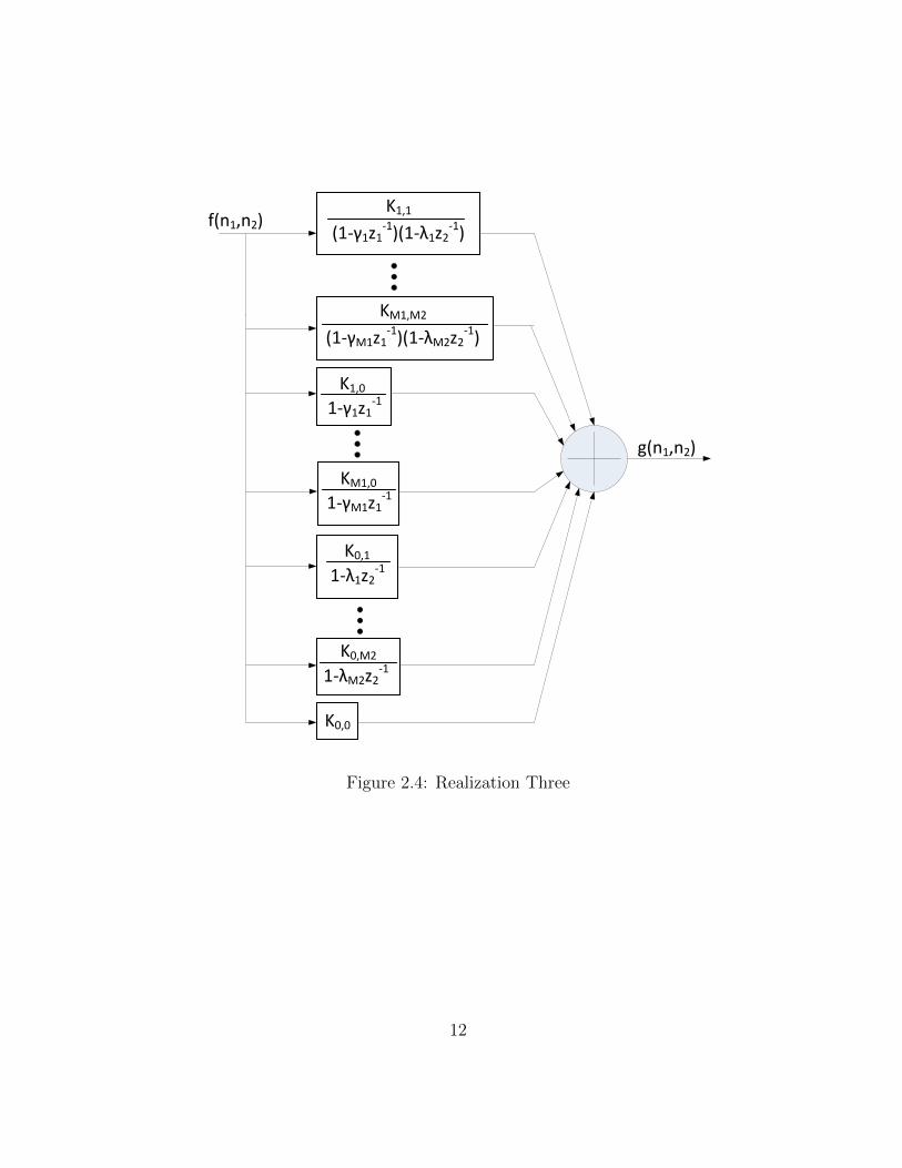
f(n1,n2)
g(n1,n2)
K0,0
K0,M2
1-λM2z2-1
K0,11-λ1z2-1
KM1,0
1-γM1z1-1
K1,01-γ1z1-1
KM1,M2
(1-γM1z1-1)(1-λM2z2-1)
K1,1(1-γ1z1-1)(1-λ1z2-1)
Figure 2.4: Realization Three
12

f(n1,n2) Z1-1 Z2
-1
γ1 λ1
K1,1
Z1-1 Z2
-1
γM1 λM2
KM1,M2
Z1-1 Z2
-1
γ1 0
K1,0
Z1-1 Z2
-1
γM1 0
KM1,0
Z1-1 Z2
-1
0 λ1
Z1-1 Z2
-1
0 λM2
K0,1
K0,M2
Z1-1 Z2
-1
0 0
K0,0
g(n1,n2)
Figure 2.5: Realization Three Implementation
13
The throughput delay of this implementation is limited by the realization of each ofthe sub-transfer functions
Hi,j(z1, z2) =Ki,j
(1− γiz−11 )(1− λjz−1
2 )(2.22)
One realization is shown in Figure 2.5. The filter can be broken down into threesubfilters – two adder-multiplier processor connected back to back, followed by a singlemultiplier and a final adder that sums up all the intermediate outputs. The implementationof the filter has a number of processors (P ) and a cycle time (T ) given as:
P = 3M1M2 + 2(M1 +M2) (2.23)
T = tmult + tadd (2.24)
where the number of processor used does not include the number of adders required toimplement the pipelined summation adder. The number of processors required is higherthan both realization one and two due to the duplicate realization of the poles. Thisstructure, however, maintains a highly parallelized pipeline and is quite suitable for multi-processor implementation.
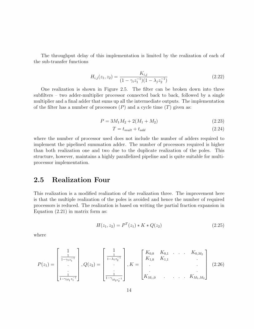
2.5 Realization Four
This realization is a modified realization of the realization three. The improvement hereis that the multiple realization of the poles is avoided and hence the number of requiredprocessors is reduced. The realization is based on writing the partial fraction expansion inEquation (2.21) in matrix form as:
H(z1, z2) = P T (z1) ∗K ∗Q(z2) (2.25)
where
P (z1) =
11
1−γ1z−11
.
.1
1−γM1z−11
, Q(z2) =
11
1−λ1z−12
.
.1
1−γM2z
−12
, K =
K0,0 K0,1 . . . K0,M2
K1,0 K1,1 .. .. .
KM1,0 . . . . KM1,M2
(2.26)
14

Equation (2.25) suggests realizing H(z1, z2) as a pipeline of three stages. The first stageis a parallel realization of the vector P (z1). The second stage is the vector-multiplicationoperations on the columns of the matrix K followed by vector-summation operations. Thethird stage is the parallel realization of the vector Q(z2) followed by summation operations.The complete realization is shown in Figure 2.6.
f(n1,n2) Z1-1
γ1
K0,0
Z1-1
γM1
λM2
KM1,0
Z1-1
0 K1,0
K0,1
KM1,1
K1,1
K0,M2
KM1,M2
K1,M2
Z2-1
0
Z2-1
λ1
Z2-1
g(n1,n2)
Figure 2.6: Realization Four.
The elements in P (z1) can be realized in parallel in one addition and one multiplication.The second stage involves parallel multiplication and addition, which can be implementedin parallel and pipeline fashion such that the cycle time is not increased, except for aninitial delay. The third stage has a similar structure to the first stage, therefore it has thesame cycle time as the first stage. The required number of processors (P ) and the cycletime (T ) are:
P = M1M2 + 2(M1 +M2) (2.27)
T = tmult + tadd (2.28)
It is worthwhile to note that the number of processors required is much less than
15

the previous realizations. In addition, this implementation can take advantage of highlyparallelized addition and multiplication when calculating the intermediate state variables.
16

Chapter 3
Filter Coefficients Derivation
In order to apply a 2D separable denominator digital filter to two dimensional data, thecorresponding filter coefficients must be first derived before data can be processed. Thederived filter coefficients can then be used to verify the functional correctness of the imple-mentation. A numerical example is taken out of existing publication in order to derive thecoefficients. The 2D impulse response specification for a Quarter-Plane Gaussian Filter[14] is given by:
hd(m,n) = 0.256322 · exp[−0.103203(m− 4)2 + (n− 4)2] (3.1)
The resulting 2D separable denominator digital filter is given by Roesser local state-space (LSS) matrices:[
xh(i+ 1, j)xv(i, j + 1)
]=
[A1 A2
0 A4
] [xh(i, j)xv(i, j)
]+
[b1b2
]u(i, j) (3.2)
y(i, j) =[c1 c2
] [xh(i, j)xv(i, j)
]+ du(i, j) (3.3)
where xh(i, j) is a M1× 1 horizontal state vector, xv(i, j) is a M2× 1 vertical state vector,u(i, j) is a scalar input, y(i, j) is a scalar output, and
A1 =
0.86382 0.27191 0.03899−0.27191 0.59513 −0.360790.03899 0.36079 0.35615
(3.4)
17

A2 =
0.42903 0.33791 −0.129900.33791 0.26614 −0.10231−0.12990 −0.10231 0.03933
(3.5)
A4 =
0.86382 −0.27191 0.038990.27191 0.59513 0.360790.03899 −0.36079 0.35615
(3.6)
bt1 =[0.06361 0.05010 −0.01926
](3.7)
bt2 =[0.65500 −0.51589 −0.19831
](3.8)
c1 =[0.65500 −0.51589 −0.19831
](3.9)
c2 =[0.06361 0.05010 −0.01926
](3.10)
D = 0.00943 (3.11)
To derive the coefficients required for the realizations, the local state-space matricesneed to be converted to a transfer function. Assume there is no loss of generality inrepresenting 2D separable denominator digital filters by the LSS model in Equation 3.2and 3.3. The LSS model is assumed to be asymptotically stable and minimal. The transferfunction is given by [15]
H(z1, z2) =[c1 c2
] [z1IM1 − A1 −A2
0 z2IM2 − A4
]−1 [b1b2
]+ d (3.12)
=[1 c1(z1IM1 − A1)
−1] [d c2b1 A2
] [1
(z2IM2 − A4)−1b2
](3.13)
By applying this transform, the resulting transfer function is:
H(z1, z2) =i(z1, z2)
j(z1)× k(z2)(3.14)
18

where
i(z1, z2) = 0.009059397520z−31 z−3
2 + 0.007524922930z−31 z−2
2 + 0.002468223450z−31 z−1
2 +
0.009244024377z−31 + 0.007524922933z−2
1 z−32 + 0.006245656370z−2
1 z−22 +
0.00205458569z−21 z−1
2 + 0.007675175463z−21 + 0.002468223444z−1
1 z−32 +
0.00205458571z−11 z−2
2 + 0.000668282136z−11 z−1
2 + 0.00252151860z−11 +
0.009244024371z−32 + 0.00767517545z−2
2 + 0.00252151860z−12 +
0.00943
j(z1) =1
1− 1.515100000z−11 + 1.236274491z−2
1 − 0.3133116076z−31
k(z2) =1
1− 1.515100000z−12 + 1.236274491z−2
2 − 0.3133116076z−32
Factoring the denominator of j(z1) and k(z2) gives:
j(z1) =1
(1− 0.3945011412z−11 )(1− 1.120598859z−1
1 + 0.7941969614z−21 )
=1
(1− 0.3945011412z−11 )(0.560295295 + 0.6562328205iz−1
1 )·
1
(0.560295295− 0.6562328205iz−11 )
and
k(z2) =1
(1− 0.3945011412z−12 )(1− 1.120598859z−1
2 + 0.7941969614z−22 )
=1
(1− 0.3945011412z−12 )(0.560295295 + 0.6562328205iz−1
2 )·
1
(0.560295295− 0.6562328205iz−12 )
19

so, the filter has two real poles at:
z1 = z2 = 0.3945011412
and four imaginary poles at:
z1 = z2 = 0.560295295± 0.6552328205i
3.1 Realization One
Since the transfer function of realization one can be written as a product of two functionsas shown in Equation 2.2, Equation 2.3, and Equation 2.4 , the filter coefficients can bedirectly collected from the transfer function without any transformation as follows:
α0 = β0 = 1
α1 = β1 = −1.5151
α2 = β2 = 1.236274491
α3 = β3 = −0.3133116076
20

b3,3 = 0.009059397520
b3,2 = 0.007524922930
b3,1 = 0.002468223450
b3,0 = 0.009244024377
b2,3 = 0.007524922933
b2,2 = 0.006245656370
b2,1 = 0.00205458569
b2,0 = 0.007675175463
b1,3 = 0.002468223444
b1,2 = 0.00205458571
b1,1 = 0.000668282136
b1,0 = 0.00252151860
b0,3 = 0.009244024371
b0,2 = 0.00767517545
b0,1 = 0.00252151860
b0,0 = 0.00943000000
3.2 Realization Two
The filter coefficients for realization two are obtained from the decomposition of the matrixB into two submatrices. As shown in Equation 2.9, the numerator of the transfer functionis separated into three matrices. Lower-Upper (triangular) Decomposition is used here todecompose the matrix B into a product of two matrices using Matlab.
p(z1, z2) =
M1∑i=0
M2∑j=0
bi,jz−i1 z
−j2 = ZT
1 ·B · Z2 = ZT1 · L · U · ZT
2 = (ZT1 · L)(U · Z2) (3.15)
and from Matlab, matrix B is:
21

L =
1 0 0 0
0.026739327677625 1 0 00.081391044114528 −0.385454286773350 1 00.980278299363733 0.598912923175959 0.166861870971349 1
(3.16)
U =
0.0943 0.0025215186 0.00767517545 0.00924402437
0 −0.000005954980906 0.000001995405592 −0.0000035665228940 0 −0.000000479927738 −0.0000002597514830 0 0 −0.000000139588430
(3.17)
The denominator coefficients remain the same as realization one.
α0 = β0 = 1
α1 = β1 = −1.5151
α2 = β2 = 1.236274491
α3 = β3 = −0.3133116076
However, the numerator coefficients is less straightforward. According to Equation 2.14and Equation 2.15, the filter coefficients that are z1-dependent are denoted gk1 and filter co-efficients that are z2-dependent are denoted hkj, where k represents the corresponding filtercoefficients for each set of subfilters containing only one z1 subfilter and one z2 subfilter.
22
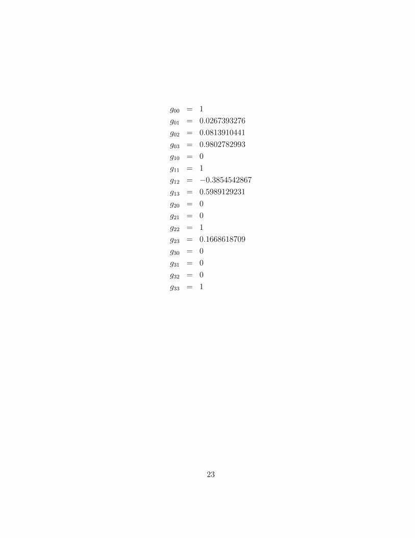
g00 = 1
g01 = 0.0267393276
g02 = 0.0813910441
g03 = 0.9802782993
g10 = 0
g11 = 1
g12 = −0.3854542867
g13 = 0.5989129231
g20 = 0
g21 = 0
g22 = 1
g23 = 0.1668618709
g30 = 0
g31 = 0
g32 = 0
g33 = 1
23

h00 = 0.0943
h01 = 0.0025215186
h02 = 0.00767517545
h03 = 0.00924402437
h10 = 0
h11 = −0.0000059549
h12 = 0.0000019954
h13 = −0.0000035665
h20 = 0
h21 = 0
h22 = −0.0000004799
h23 = −0.0000002597
h30 = 0
h31 = 0
h32 = 0
h33 = −0.0000001395
3.3 Realization Three
In order to produce the filter coefficients for realization three, the transfer function ispartial fraction expanded and then its fraction numerator is solved. The chosen transferfunction, however, contains four complex roots and two real roots. As a result, each twocomplex conjugate roots are combined to produce a real second order polynomial.
According to Equation 2.21, a 2D separable denominator digital filter of order 3 × 3 hasthe general partial fraction expanded form:
24

H(z1, z2) =K1
(1− γ1z−11 )(1− λ1z−1
2 )+
K2
(1− γ1z−11 )(1− λ2z−1
2 )+
K3
(1− γ1z−11 )(1− λ∗2z−1
2 )+
K4
(1− γ2z−11 )(1− λ1z−1
2 )+
K5
(1− γ2z−11 )(1− λ2z−1
2 )+
K6
(1− γ2z−11 )(1− λ∗2z−1
2 )+
K7
(1− γ∗2z−11 )(1− λ1z−1
2 )+
K8
(1− γ∗2z−11 )(1− λ2z−1
2 )+
K9
(1− γ∗2z−11 )(1− λ∗2z−1
2 )+
K10
(1− γ1z−11 )
+K11
(1− γ2z−11 )
+
K12
(1− γ∗2z−11 )
+K13
(1− λ1z−12 )
+K14
(1− λ2z−12 )
+K15
(1− λ∗2z−12 )
+K16
=K1
(1− γ1z−11 )(1− λ1z−1
2 )+
(K2 +K3)z−12 + (K2 +K3)
(1− γ1z−11 )(1− β1z−1
2 − β2z−22 )
+
(K4 +K7)z−11 + (K4 +K7)
(1− α1z−11 − α2z
−21 )(1− λ1z−1
2 )+
{(K5 · γ∗2 · λ∗2 +K9 · −γ2 · −λ2)z−11 z−1
2 +
(K5 · −γ∗2 +K9 · −γ2)z−11 + (K5 · −λ∗2 +K9 · −λ2)z−1
2 + (K5 +K9)} ·1
(1− α1z−11 − α2z
−12 )(1− β1z−1
1 − β2z−12 )
+
{(K8 · −γ2 · −λ∗2 +K6 · −γ∗2 · −λ2)z−11 z−1
2 +
(K8 · −λ∗2 +K6 · −λ2)z−12 + (K8 · −γ2 +K6 · −γ∗2)z−1
1 + (K8 +K6)} ·1
(1− α1z−11 − α2z
−12 )(1− β1z−1
2 − β2z−12 )
+
K10
1− γ1z−1 1+
(K11 · −γ∗2 +K12 · −γ2)z−11 + (K11 +K12)
1− α1z−11 − αz−2
1
+
K13
1− λ1z−12
+(K14 · −λ∗2 +K15 · −λ2)z−1
2 + (K14 +K15)
1− β1z−12 − βz−2
2
+K16
After collecting similar powers and reducing, this simplifies to:
25

H(z1, z2) =Az−1
1 z−12 +Bz−1
1 + Cz−12 +D
(1− α1z−11 − α2z
−21 )(1− β1z−1
2 − β2z−22 )
+ (3.18)
E
(1− γ1z−11 )(1− λ1z−1
2 )+ (3.19)
Fz−12 +G
(1− γ1z−11 )(1− β1z−1
2 − β2z−22 )
+ (3.20)
Hz−11 + I
(1− α1z−11 − α2z
−21 )(1− λ1z−1
2 )+ (3.21)
J
(1− γ1z−12 )
+ (3.22)
Kz−11 + L
(1− α1z−11 − α2z
−21 )
+ (3.23)
M
(1− λ1z−12 )
+ (3.24)
Nz−12 +O
(1− β1z−12 − β2z−2
2 )+ P (3.25)
Solving this system of 16 linear equations using matrices yields:
A · x = B (3.26)
where A is a matrix of dimension 16 × 16, and B is a column of dimension 16 × 1 andx represents the filter coefficients of dimension 1 × 16. Furthermore, matrix A is dividedinto four submatrices 1.
A =
[A1 A2
A3 A4
](3.27)
1A1, A2, A3, and A4 displayed here are with reduced precision due to page size restriction. Actualmatrix precision is 10 digits after the decimal point.
26

A1 =
0 0 0 1 1 0 1 00 0 1 −0.6636 −1.1514 1 −0.6636 00 0 −0.6636 0 0.4721 −0.6636 0 00 0 0 0 0 0 0 00 1 0 −0.6636 −1.1514 0 −1.1514 11 −0.6636 −0.6636 0.4403 1.3259 −1.1514 0.7641 −1.1514
−0.6636 0 0.4403 0 −0.5436 0.7641 0 0.47210 0 0 0 0 0 0 0
(3.28)
A2 =
1 1 0 1 1 0 1 11.1514 1.8151 0 1.8151 1.1514 1 0.6636 1.81510.4721 1.2362 0 1.2362 0.4721 −0.6636 0 1.2362
0 −0.3133 0 −0.3133 0 0 0 −0.3133−0.6636 −1.1514 1 −0.6636 −1.8151 0 −1.8151 −1.81510.7641 2.0900 −1.8151 1.2045 2.0900 −1.8151 1.2045 3.2945−0.3133 −1.4235 1.2362 −0.8203 −0.8569 1.2045 0 −2.2439
0 0.3607 −0.3133 0.2079 0 0 0 0.5686
(3.29)
A3 =
0 −0.6636 0 0 0.4721 0 0.4721 −0.6636−0.6636 0.4403 0 0 −0.5436 0.4721 −0.3133 0.76410.4403 0 0 0 0.2229 −0.3133 0 −0.3133
0 0 0 0 0 0 0 00 0 0 0 0 0 0 00 0 0 0 0 0 0 00 0 0 0 0 0 0 00 0 0 0 0 0 0 0
(3.30)
27

A4 =
0 0.4721 −0.6636 0 1.2362 0 1.2362 1.23620 −0.8569 1.2045 0 −1.4235 1.2362 −0.8203 −2.24390 0.5836 −0.8203 0 0.5836 −0.8203 0 1.52830 −0.1479 0.2079 0 0 0 0 −0.38730 0 0 0 −0.3133 0 −0.3133 −0.31330 0 0 0 0.3607 −0.3133 0.2079 0.56860 0 0 0 −0.1479 0.2079 0 −0.38730 0 0 0 0 0 0 0.09816
(3.31)
and
B =
0.009430000000.002521518600.007675175450.009244024360.002521518600.000668282130.002054585710.002468223440.007675175460.002054585690.006245656350.007524922930.009244024360.002468223450.007524922930.00905939752
(3.32)
Solving the system of linear equations, by x = A \B , the solution is obtained.
28

x =
−2.13997007282.63156022631.4059630793−1.1315043079−1.4883426863−2.36318178752.2515878795−2.36318178640.52898585339−0.57836003994−0.203368090400.45656755241−0.57836003983−0.203368090350.456567552310.092288236346
(3.33)
Referring to Equation 3.18 to Equation 3.25, the coefficients are then 2:
2Variable A and B presented here are coefficients for the partial fraction expanded 2D transfer functionin Equation 3.18
29

A = −2.1399700728
B = 2.6315602263
C = 1.4059630793
D = −1.1315043079
E = −1.4883426863
F = −2.3631817875
G = 2.2515878795
H = −2.3631817864
I = 0.52898585339
J = −0.57836003994
K = −0.20336809040
L = 0.45656755241
M = −0.57836003983
N = −0.20336809035
O = 0.45656755231
P = 0.092288236346
3.3.1 Modification to Realization Three
In Section 2.4, an architecture suitable for M1 ×M2 filter order is presented. However, therealization presented assume all the roots are real. As shown in Equation 3.18 to Equation3.25, the roots are not all real. The roots shown in the numerical example are a singlereal, a complex, and a complex conjugate root in both the z1 and z2 direction. Due to thisproblem, the realization needs to be modified before it is suitable for implemention.
In order to accommodate complex roots, the complex roots are combined to form a realpolynomial of order two that is realized using transposed direct form II. Figure 3.1(a) is thesubfilter for realizing the combined complex roots in the z1 direction and Figure 3.1(b) forthe z2 direction. Since the numerator is no longer a constant, but also contains coefficientsmultiplied by delays in z1 and z2 dimension, the numerator needs to to be modified aswell. The transposed direct form of FIR filter is suitable to implement the numerator.Figure 3.1(c) shows the modified realization to implement the numerator portion of thefirst double root containing coefficients A, B, C and D in the form:
30

Az−11 z−1
2 +Bz−11 + Cz−1
2 +D
(1− αz−11 − αz−2
1 )(1− βz−12 − βz−2
2 )(3.34)
1-1
w(n1,n2)f(n1,n2)
1-1
1
2
1-1
1-1
u0(n1,n2) g(n1,n2)
u1(n1,n2)
u2(n1,n2)
1
2
1-1
1-1
1-1
1-1
u0(n1,n2)
u1(n1,n2)
w(n1,n2)
(a) Modified z1 subfilter
1-1
w(n1,n2)f(n1,n2)
1-1
1
2
1-1
1-1
u0(n1,n2) g(n1,n2)
u1(n1,n2)
u2(n1,n2)
1
2
1-1
1-1
1-1
1-1
u0(n1,n2)
u1(n1,n2)
w(n1,n2)
(b) Modified multiplier subfilter
Z1-1
w(n1,n2)f(n1,n2)
Z1-1
-α1
-α2
Z2-1
Z2-1
u0(n1,n2) g(n1,n2)
u1(n1,n2)
u2(n1,n2)
-β1
-β2
Z1-1 Z1
-1
Z1-1 Z1
-1
A
u0(n1,n2)
u1(n1,n2)
w(n1,n2)
B D
C
(c) Modified z2 subfilter
Figure 3.1: Implementation for the Numerator and the Denominator for Equation 3.34.
A detailed subfilter realization is shown in Appendix A.3.
3.4 Realization Four
Realization four is a modified version of realization three, where redundant implementationof the same pole is avoided. Coefficients involving the same pole are summed using a treeadder and then multiplied by the pole. As such, the coefficients used for realization fourare the same as the coefficients used for realization three, which are presented in Section3.3.
Writing realization four in matrix form using the derived coefficients A to P:
H(z1, z2) = P T (z1) ·K ·Q(z2) (3.35)
where
31

P (z1) =
11
(1−γ1z−11 )
1(1−α1z
−11 −α2z
−21 )
, Q(z2) =
11
(1−λz−12 )
1(1−β1z−1
1 −β2z−21 )
(3.36)
K =
P M Nz−12 +O
J E Fz−12 +G
Kz−11 + L Hz−1
1 + I Az−11 z−1
2 +Bz−11 + Cz−1
2 +D
(3.37)
The filter realization have the structure similar to realization three. The circuitry thatrealizes the z1 and z2 poles and the coefficients is the same as the one shown in Figure3.3.1. The difference, however, is that this realization does not realize the same polemultiple times. As a result, the wire connection will be different for realization four fromrealization three. A detailed subfilter realization is shown in Appendix A.4.
32

Chapter 4
Timing Considerations on FilterImplementation
Before the system architecture of the digital signal processor can be presented, the timingof the filter realizations must be first investigated. As a whole, digital circuits are composedof two types of paths: data paths and control paths. Data paths propagate the data alongan arithmetic channel while the control paths moderate the flow and the direction of thedata traveling on the data paths. Some paths are timing critical, which implies that thepaths are affecting the speed at which the design can operate. Therefore critical pathsmust be identified and optimized in order to improve the filter throughput.
Since the feedback paths stipulate the shortest time for which the output of the previoussubfilter can be transferred to the input of the following subfilter, the feedback paths arealso considered the critical paths. In this chapter, the critical path for each of the fourrealizations are identified and modifications are made to improve the performance.
4.1 Critical Data Path in Realization One
Since realization one is comprised of three subfilters, each subfilter will have a critical path.The critical path of the implementation is therefore the maximum of the three criticalpaths. For the first subfilter, the critical path is two adds and one multiply. For the secondsubfilter, the critical path is one multiply and one add. For the third subfilter, the criticalpath is two adds and one multiply. The three input adder in the third subfilter is brokendown into two adders connected in series. The critical paths for the first, second and third
33

stages are shown in Figure 4.1. The actual throughput delay for the implementation istherefore two adds, one multiply plus one additional clock cycle required for the horizontaldelay element to transfer the data from previous stage to the next stage. Next, sincethe subfilters are connected in cascade, critical path for the overall realization must beidentified.
Z11
Z1-1 Z1
-1
Z1-1 Z1
-1
Z2-1
Z2-1Feedback Path
Z1-1
w(n1,n2)
Z1-1 Z1
-1
w(n1,n2)
Z2-1
u0(n1,n2)
u1(n1,n2)
g(n1,n2)
Z2-1
f(n1,n2)
Three input adder
u0(n1,n2)
(a) First stage
Z11
Z1-1 Z1
-1
Z1-1 Z1
-1
Z2-1
Z2-1Feedback Path
Z1-1
w(n1,n2)
Z1-1 Z1
-1
w(n1,n2)
Z2-1
u0(n1,n2)
u1(n1,n2)
g(n1,n2)
Z2-1
f(n1,n2)
Three input adder
u0(n1,n2)
(b) Second stage
Z1-1
Z2-1
u0(n1,n2)
u1(n1,n2)
g(n1,n2)
Z2-1
Three input adder
Z1-1 Z1
-1 Z1-1
u0(n1,n2)
Z1-1
u0(n1-1,n2)Z1
-1
(c) Third Stage
Figure 4.1: Critical Paths in First, Second and Third Subfilter of Realization One.
In the original realization shown in Figure 2.1, the critical path with the three subfilterscombined is three add and one multiply, which is larger than the critical path of the indi-vidual subfilters. If the design remains unchanged, the throughput of the implementationwill be three add and one multiply as shown in Figure 4.2(a) since the longest critical pathdictates how fast the entire realization can be clocked. To increase the throughput, anadditional horizontal delay is introduced at the output of the second subfilter. This hori-zontal delay breaks the overall critical path such that the overall implementation retains athroughput of two add and one multiply. However, since an extra horizontal delay is added,the output ui(n1, n2) and g(n1, n2) now have an additional horizontal delay, as shown in
34

Figure 4.2(b). This extra horizontal delay adds to the overall latency of the digital filter,but does not affect the processed data in any way.
Z2-1
u0(n1,n2)
u1(n1,n2)
g(n1,n2)
Z1-1 Z1
-1
u0(n1-1,n2)Z1
-1 Z1-1 Z1
-1
Z1-1
f(n1,n2)
Z1-1
f(n1,n2)
g(n1-1,n2)
(a) Critical path of the overall realization
u1(n1,n2)
2-1
u0(n1-1,n2)
u1(n1-1,n2)
1-1
1-1
1-11
-1
f(n1,n2)
g(n1-1,n2)
(b) Modified critical path of the overall realization
Figure 4.2: Critical Path and Modified Critical Path for Realization One.
35

4.2 Critical Data Path in Realization Two
Realization two contains two subfilters and a tree adder. Each subfilter has its own criticalpath, while the tree adder can be adjusted to accommodate the critical path found in theprevious two subfilters. For the first subfilter, the critical path is one multiply and twoadds. For the second subfilter, the critical path is also one multiply and two adds. Thecritical paths for the first and second subfilter is shown in Figure 4.2.
Z1-1 Z1
-1 Z1-1
-αM1 -αM1-1 -α1
f(n1,n2)
gk,M1
Z2-2 Z2
-2 Z2-2
-βM2
hk,M2
wr(n1,n2)
vr(n1,n2)-β1-βM2-1
gk-1,M1 g1,M1 g0,M1
hk-1,M2 h1,M2 0,M2
(a) First stage
Z1-1 Z1
-1 Z1-1
-αM1 -αM1-1 -α1
f(n1,n2)gk,M1
Z2-2 Z2
-2 Z2-2
-βM2
hk,M2
wr(n1,n2)
wr(n1,n2)
vr(n1,n2)-β1-βM2-1
Z1-1 Z1
-1
Z2-2 Z2
-2
f(n1,n2)
Z1-1
vr(n1,n2)
gk-1,M1 g1,M1 g0,M1
hk-1,M2 h1,M2 h0,M2
gk,0gk,M1
-αM1 -α1
-βM2 -β1
hk,0hk,M2
(b) Second stage
Figure 4.3: Critical Paths in First, Second and Third Stages of Realization Two.
In the original realization shown in Figure 2.3, the critical path with the two subfilters com-bined is two add and two multiply, which is larger than the critical path of the individualsubfilters. If the design remains unchanged, the throughput of the implementation will betwo add and two multiply as shown in Figure 4.4(a) since the longest critical path dictateshow fast the entire realization can be operated. To increase the throughput, an additionalhorizontal delay is introduced at the output of the first subfilter. This horizontal delaybreaks the overall critical path so that the overall implementation retains a throughput oftwo add and one multiply. Since an extra horizontal delay is added, the output g(n1, n2)now has an additional horizontal delay, as shown in Figure 4.4(b). This extra horizontaldelay increases the overall latency of the digital filter by one, but does not affect the outputdata. Since the minimum throughput is determined to be two add and one multiply, thetree adder that sums up all the vr(n1, n2) can now be determined to have two adds in its
36

critical path.
Z1-1 Z1
-1
Z2-2 Z2
-2
f(n1,n2)
Z2-2 Z2
-2 Z2-2
β
hk,M2
wr(n1,n2)
vr(n1,n2)
vr(n1,n2)
ββ
Z1-1 Z1
-1
Z2-2 Z2
-2
f(n1,n2)
Z1-1
vr(n1,n2)
hk-1,M2 h1,M2 h0,M2
-αM1 -α1
gk,M1 gk,1 gk,0
-βM2 -β1
hk,M2 hk,1 hk,0
gk,0gk,M1
-αM1 -α1
-βM2 -β1
hk,0hk,M2
(a) Critical path of the overall realization
Z1-1 Z1
-1
Z2-2 Z2
-2
f(n1,n2)
Z2-2 Z2
-2 Z2-2
-βM2
hk,M2
wr(n1,n2)
vr(n1,n2)
vr(n1,n2)
-β1-βM2-1
Z1-1 Z1
-1
Z2-2 Z2
-2
f(n1,n2)
Z1-1
vr(n1-1,n2)
hk-1,M2 h1,M2 h0,M2
-αM1 -α1
gk,M1 gk,1 gk,0
-βM2 -β1
hk,M2 hk,1 hk,0
gk,0gk,M1
-αM1 -α1
-βM2 -β1
hk,0hk,M2
(b) Modified critical path of the overall realization
Figure 4.4: Critical Path and Modified Critical Path for Realization Two.
37

4.3 Critical Data Path in Realization Three and Four
Despite the structural difference between realization three and realization four, the basicsubfilter that is used to construct realization three and realization four is the same. Thez1 and z2 denominator realization is shown in Figure 4.5(a) and 4.5(b). In fact, this samedenominator realization is used in realization one. The critical path is then two adds andone multiply as previously discussed.
-α1Z1-1 Z1-1
b3,0 b2,0
Z1-1 Z1-1
b3,1 b2,1
-β2
-β1
Z2-1
Z2-1
Z1-1
f(n1,n2)
Z1-1
-α2
g(n1,n2)
(1-γ1z1-1)(1-λ1z2-1)
Z1-1
f(n1,n2)
-γ1
g1(n1,n2)
-λ1
Z2-1Z1-1
E
(a) z1 denominator real-ization
-α1Z1-1 Z1-1
b3,0 b2,0
Z1-1 Z1-1
b3,1 b2,1
-β2
-β1
Z2-1
Z2-1
Z1-1
f(n1,n2)
Z1-1
-α2
g(n1,n2)
(1-γ1z1-1)(1-λ1z2-1)
Z1-1
f(n1,n2)
-γ1
g1(n1,n2)
-λ1
Z2-1Z1-1
E
(b) z2 denominator real-ization
Figure 4.5: Denominator Realization for Realization Three and Four.
The numerator realization is similar to realization one. One horizontal delay is inserted atthe end of the FIR filter chain to ensure a throughput of two add and one multiply. Thenumerator subfilter which realizes coefficient A, B, C, and D is shown in Figure 4.6.
Both realization three and four share the same subfilters for denominator and numera-tor realization. The only difference is realization four eliminates multiple realization ofthe same pole. This results in reduced hardware utilization and lower power dissipation.Appendix A.3 shows the detailed realization three subfilters and Appendix A.4 shows thedetailed realization four subfilters.
38

-α1Z1-1 Z1-1
B D
Z1-1 Z1-1
A C
-β2
-β1
Z2-1
Z2-1
Z1-1
f(n1,n2)
Z1-1
-α2
g(n1,n2)
(1-γ1z1-1)(1-λ1z2-1)
Z1-1
f(n1,n2)
-γ1
g1(n1,n2)
-λ1
Z2-1Z1-1
E
Figure 4.6: Numerator Realization
39

4.4 Control Path
Since adders, multipliers and shift registers are connected in series for all the realizations,control paths are required to reduce inadvertent data shifts. An example is provided toillustrate the significance of control paths. The example used for this section is subfilterone of realization one, as shown in Figure 4.7(a). It will be used to illustrate how incorrectdata can be inadvertently shifted without proper control paths.
1
-1
IN OUT
A
B
C
D
2
(a) Realization One subfilterone
t0 t1 t2 t3 t4 t5 t6 t7 t8 t9 t10
INOUT
ABCD
Z1-1
IN OUT
A
B
C
D
0 1
14 5 11
2 84 10
1043
2
32
INOUT
ABCD
0 1
14 11
2 810
103
32
t0 t1 t2 t3 t4 t5 t6 t7 t8 t9 t10
ENA_OUTENA_BENA_CENA_D
3
3
1012
(b) Timing diagram without control path
Figure 4.7: Example Timing Diagrams Without Control Paths.
For the sake of simplicity, an adder latency of 2 clock cycles, multiplier latency of 3clock cycles, and shift register latency of 1 clock cycle is assumed. Figure 4.7(b) shows
40

the timing diagram of such a circuit assuming both adders, multiplier and shift registerare operating simultaneously. Before zero time unit (t0), IN is given the initial value of0, A the value of 1, D the value of 3. Since OUT is the sum of IN and D, it is given thevalue of 3. For the same reason, C is the sum of A and B, and is given the value of 3,provided that the coefficient for the multiplier is 2 as shown. At zero time unit (t0), INswitches from 0 to 1 and A switches from 1 to 2. After 2 time unit (t2), adder on the tophas finished calculating and OUT switches from 1 to 4. Since the adder on the bottomis calculating simultaneously as the top adder, C switches from 3 to 4. After 1 time unit(t3), C has propagated to D via shift register, and D switches from 3 to 4. After 2 timeunit (t5), the multiplier has finished calculating and B switches from 2 to 8. At the sametime, OUT switches from 4 to 5 due to a change on D. This result is undesirable since thechange on OUT is propagated due to toggling of A to C to D. The correct result is finallyattained after 5 time unit (t10), when OUT switches from 5 to 11. Without proper control,the incorrect intermediate sum will propagate further down the signal processing pipelineand results in rapid toggling at the output. Clearly a control circuit is needed to remedythe problem.
To remedy the propagation of incorrect intermediate sums, a control circuitry is used toenable the adders, multiplier and shift register at the proper time. To produce the correctsum for the sample circuit in Figure 4.7(a), the top adder, the multiplier, the bottom adder,and the shift register must be enabled in this order. Figure 4.8 shows the enable signalsthat drive the corresponding output. ENA OUT signals the top adder to turn on for twoclock cycles to produce the correct sum at t2. Following that, ENA B signals the multiplierto turn on for 3 clock cycles to produce the correct product at t5. ENA C and ENA Dsignals are applied to the bottom adder and the shift register to produce the correct sum.Notice the erroneous value of 5 no longer appears on OUT at t5 using this control scheme.
Since all the realizations use a similar configuration of a multiplier, adders, and shiftregisters, the control scheme is applied to all the realizations to prevent incorrect calcula-tions from propagating down the signal processing pipeline. This change in architecture isof course subject to trade-offs. Since extra circuitry is used to produce the correct enablesignals for the corresponding adders, multipliers and shift registers, the hardware utiliza-tion will increase. Furthermore, additional routing resources are needed to fit the designas well.
Even though the same control scheme is applied to all four realizations, the exact cycletime required is different from one realization to another. The timing sequence shown inFigure 4.8 applies directly to realization one and realization two, since the critical pathis two adds, one multiply and one horizontal shift. For realization three and realizationfour, however, the timing sequence is different. The critical path is actually one add, one
41

t0 t1 t2 t3 t4 t5 t6 t7 t8 t9 t10
INOUT
ABCD
Z1-1
IN OUT
A
B
C
D
0 1
14 5 11
2 84 10
1043
2
32
INOUT
ABCD
0 1
14 11
2 810
103
32
t0 t1 t2 t3 t4 t5 t6 t7 t8 t9 t10
ENA_OUTENA_BENA_CENA_D
3
3
1012
Figure 4.8: Timing Diagram with Control Path.
Table 4.1: Cycle Time for Each Realization.Realiation Cycle Time
One 2tadd + tmult + 1Two 2tadd + tmult + 1
Three tadd + tmult + 1Four tadd + tmult + 1
multiply and one horizontal shift. Table 4.1 summarizes the cycle time for each realization.
42

Chapter 5
System Implementation Details
To implement a 2D separable denominator digital filter and use it to process two dimen-sional data, a complete system is required to receive input from a source, buffer the inputdata, process the data using the digital filter, buffer the output data, and send the outputdata back to the source.
There are two ways to produce a robust and reusable system: full-custom ASIC flowor FPGA flow. A full-custom ASIC flow is a long and arduous process involving manyspecific design tools, as shown on the right hand side of Figure 5.1. The circuitry is firstdesigned, functionally simulated, synthesized, layed out, manufactured and then tested.The entire process can occupy months for just one iteration of the design. The finishedproduct is much more compact and better optimized in both power and performance whencompared to an FPGA board.
On the contrary, the FPGA design flow is much more flexible and forgiving whencompared to the ASIC flow. One iteration of the design from synthesis, place and routeto testing can be done in a fraction of time that ASIC flow takes. The FPGA board canbe reused many times, unlike ASIC which needs to be replaced with each new revision.Furthermore, many FPGA vendors handle both the front-end as well as back-end tasks inone manageable piece of software, saving both cost and precious development time. As aresult, the digital signal processing system is built using a FPGA design flow, as shown onthe left hand side of Figure 5.1. In the next section, the advantages and disadvantages ofusing fixed point versus floating point arithmetic for the digital signal processing systemis discussed.
43

Figure 5.1: FPGA versus ASIC Design Flow
44

5.1 Fixed Point versus Floating Point
Traditional digital filters are implemented with fixed point calculations in mind, with whichcalculations are made with limited precision. Nowadays, hardware resources are becomingmuch cheaper and it is not unconventional to find floating point digital filters with muchhigher precision, albeit at the cost of higher hardware utilization as well. It is not an easychoice to make when it comes down to using fixed point or floating point arithmetic units,since both fixed point and floating point have advantages and disadvantages.
Fixed point processing is susceptible to finite word length effects, which occurs whenthe word length of the registers is less than the required precision needed to store the actualvalue. These effects introduce noise into the Digital Signal Processing system and createundesirable behavior, such as input quantization noise, coefficient quantization noise andarithmetic overflow [1].
Input quantization noise arises from the limited precision of the Analog to DigitalConverter, when a continuous time signal is converted to a discrete time signal. For thecase of filters, the input data is usually pre-sampled and quantized to acceptable levelsbefore it is fed to the processors. As a result, input quantization noise is less of an issue forthe matter at hand since it is assumed that this digital filter is a part of a larger systemthat reduce input quantization noise to an acceptable level.
On top of input quantization noise, there can also be noise associated with the coeffi-cients that are used to describe the transfer function of the filter. Usually the coefficientsassume the system has infinite precision. The Digital Signal Processing system has a lim-ited amount of memory and is forced to truncate the coefficients. What is more, truncatedcoefficients no longer retain the precision of the original coefficients and can affect pole/zerolocations, thus altering the frequency response of the digital filter. This effect is especiallycritical for IIR filters where the movement of the pole locations may lead to instability.
Lastly, addition and multiplication are two common operations in a Digital SignalProcessing system. Multiplying two 16 bit number requires a 32 bit register to store theresult. If the result is then multiplied with another 16 bit number, 48 (32 + 16) bits isrequired to store the result. If there are multiple multiplications within the systems, thenumber of bits required to store the intermediate output can increase very quickly. Asa result, in a fixed point Digital Signal Processing system, results are usually roundedor truncated. Unfortunately, rounding limits the growth of word length at the expenseof increased roundoff errors. The larger the Digital Signal Processing system, the moreroundoff errors the result can accumulate.
To deal with the shortcomings of fixed point Digital Signal Processing systems, floating
45

Table 5.1: IEEE 745 Single and Double Precision Floating Point Internal RepresentationType Sign Exponent Signficant Total Bits
Single Precision 1 8 23 32Double Precision 1 11 52 64
point adders and multipliers are used in the system. Floating point operations are intrin-sically more expensive than fixed point operations since floating point numbers take morebits to encode. Floating point operations require the operands to be aligned before calcula-tion can begin, a process called denormalization. After calculation is performed, the resultneeds to be converted back to single precision floating number, a process called normaliza-tion. Researchers agree in a pipelined DSP system, the denormalization and normalizationstage of the floating point operators can be fused to reduce hardware complexity and in-crease performance [16]. For this research, this particular optimization technique was notapplied since it requires C code. This idea, however, can be applied if the filter realizationsare to be implemented on ASIC since the designer typically has more control in the designand layout on ASIC than a FPGA.
The standard IEEE 745 describes five floating point standards and two of these arepopular among modern computing hardware: single precision and double precision. Theinternal representation of a single precision and a double precision floating point numberis shown in Table 5.1.
Single precision floating point numbers are much like numbers represented in scientificnotation. The sign bit represents the sign of the number. The exponent is an 8 bit signedinteger ranging from -128 to 127. The significant is stored with an implicit leading bit (tothe left of the binary point) with a value of 1 unless the significant is zero. The IEEE745 standard also lists four floating point number special cases: signed zero, subnormalnumbers, infinities, and not a number.
• Signed zero: Zero can represented as +0 or -0 in the IEEE floating point standard.The two values are numerically equal in computations. However, different operationscan produce either +0 or -0.
• Subnormal numbers: Subnormal values occur when the result of a floating pointoperation is smaller in magnitude than the smallest possible representable value inthe floating point number representation. Subnormal numbers are usually handledby the hardware.
46
• Infinities: Positive or negative infinity can result when a divide by zero exceptionoccurs. It is not an error and can occur just as often as any regular number.
• Not a number (NaN): Not a number is the result of an invalid floating point operation.For example, dividing zero by zero or taking the square root of negative one. Usinga NaN as an operand in an arthimetic operation will cause the result to be an NaNas well.
Fortunately, the Altera Quartus II IP MegaCore library comes with Floating Point (FP)adders and multipliers that can be configured to use single precision or double precisionfloating point, including the option to flag signed zero, subnormal numbers, infinities andNaNs. A design can also configure the FP multipliers and adders for different levels ofpipeline depth which can affect the overall operating speed, power and area of the DigitalSignal Processing system. For the implementation of this Digital Signal Processing system,IEEE single precision FP multipliers and adders are used to construct the system, sincethe system does not require the precision of double FP operators. In the next section, theoptimum level of pipeline for a floating point multiplier and an adder is discussed.
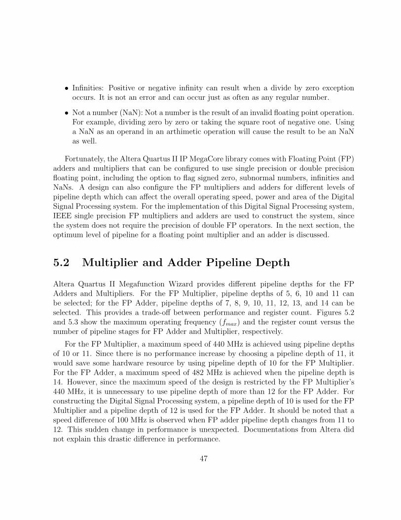
5.2 Multiplier and Adder Pipeline Depth
Altera Quartus II Megafunction Wizard provides different pipeline depths for the FPAdders and Multipliers. For the FP Multiplier, pipeline depths of 5, 6, 10 and 11 canbe selected; for the FP Adder, pipeline depths of 7, 8, 9, 10, 11, 12, 13, and 14 can beselected. This provides a trade-off between performance and register count. Figures 5.2and 5.3 show the maximum operating frequency (fmax) and the register count versus thenumber of pipeline stages for FP Adder and Multiplier, respectively.
For the FP Multiplier, a maximum speed of 440 MHz is achieved using pipeline depthsof 10 or 11. Since there is no performance increase by choosing a pipeline depth of 11, itwould save some hardware resource by using pipeline depth of 10 for the FP Multiplier.For the FP Adder, a maximum speed of 482 MHz is achieved when the pipeline depth is14. However, since the maximum speed of the design is restricted by the FP Multiplier’s440 MHz, it is unnecessary to use pipeline depth of more than 12 for the FP Adder. Forconstructing the Digital Signal Processing system, a pipeline depth of 10 is used for the FPMultiplier and a pipeline depth of 12 is used for the FP Adder. It should be noted that aspeed difference of 100 MHz is observed when FP adder pipeline depth changes from 11 to12. This sudden change in performance is unexpected. Documentations from Altera didnot explain this drastic difference in performance.
47

150
200
250
300
350
400
450
300
350
400
450
500
Register Cou
nt
Fmax (M
Hz)
fmax register count
0
50
100
200
250
4 6 8 10 12
Pipeline Depth
Figure 5.2: FP Multiplier fmax and RegisterCount versus Pipeline Depth
870
970
480
500fmax register count
770
870
440
460
670400
420
440
r Cou
nt
(MHz)
570380
400
Register
Fmax (
370
470340
360
270
370
300
320
6 8 10 12 14 16Pipeline Depth
Figure 5.3: FP Adder fmax and RegisterCount versus Pipeline Depth
The hardware resource utilization for the selected multiplier and adder is indicatedin Table 5.2. This information allows us to make a quantitative comparison on resourceutilization from the realization to the implementation later on.
Table 5.2: Hardware Utilization for FP Multiplier and FP Adder.FP Operator Combinational ALUTs Register Count DSP 18 bit Multiplier Latency
Multiplier 535 756 4 10Adder 126 357 0 12
5.3 Shift Registers
Since the horizontal shift (z1) is only one delay in pixel, it can be easily constructed usingflip flops in parallel. The vertical shift (z2), however, contains a line worth of pixels thatis the width of the image. For a 64 × 64 image, each vertical shift needs to be 64 pixelsdeep. To accomplish this, a RAM-based shift register is used from the MegaWizard Pluginmanager. The shift register is 32 bits wide to accommodate the single precision floatingpoint algorithm used in the digital signal processing pipeline and is 64 elements deep toaccommodate the image width. The hardware resource utilization used for horizontal andvertical shift register is shown in Table 5.3.
48

Table 5.3: Hardware Utilization for Horizontal and Vertical Shift Register.Shift Register Combinational ALUTs Register Count Block Memory Bits
Horizontal 0 32 0Vertical 24 13 1984
5.4 Implementation of a DSP System
A generic system is required that allows test data to be passed into the 2D digital filterand allows it to process and transport the processed data back for display. The systemmust be able to transport the data in a timely manner and without fault. Furthermore,the system must be relatively cheap to construct. First, the communication protocol mustbe determined, which is discussed in subsection 5.4.1. Second, the overall DSP systemarchitecture must be studied and developed, which is discussed in Subsection 5.4.2.
5.4.1 Communication Protocol to the FPGA
The Altera DE4 board provides many ways to accomplish the communication task sincethe board contains an array of high-speed IOs including Serial ATA, Gigabit Ethernet,PCI Express, Universal Serial Bus 2.0, and JTAG. The relevant specifications for each IOinterface are listed below [17].
• Serial ATA 3.0: Support standard 6 Gbps signal rate.
• Gigabit Ethernet: Support Ethernet frame at 1 Gbps.
• PCI Express x8: Support speed for first generation at 2.5 Gbps/lane and secondgeneration at 5 Gbps/lane. Can interface with PC motherboard with x8 or x16 PCIExpress slot.
• USB 2.0: Support speed up to 480 Mbps. Also support both USB host and device.
• JTAG: Used to program and debug the FPGA via USB adapter. Speed is limited bythe USB medium.
In fact, all these communication protocols are all viable choices and the only difference isthe communication speed. Altera has also provided sample applications which convenientlywork out of the box. The choice is then arbitrary and can be easily converted if more
49

communication protocols need to be included. The JTAG protocol is the ideal protocolto start with since it uses the existing USB cable that configures the FPGA and is thesimplest protocol to use.
In essence, the USB cable is used to download a configuration bit stream to the FPGAdevice. Once the device powers up, the USB cable switches over to JTAG mode andenables debugging of onboard components using either the Avalon Memory Mapped (MM)interface or Streaming (ST) interface. There are hardware IPs embedded on the FPGAboard that enable the required hardware transaction. The details of these hardware IPsare not discussed since they are beyond the scope of this thesis. More details with regardto Avalon MM interface and ST interface are discussed in Subsection 5.4.2.
5.4.2 DSP System Architecture
The proposed architecture of the digital signal processing system is shown in Figure 5.4.The DSP system is first configured via a byte stream from the host PC using the USBBlaster 1. JTAG to Avalon MM interface is used to write filter coefficients to the digitalfilter. The actual image data is streamed into the input FIFO, processed by the digitalfilter, streamed back to the output FIFO, and then returned to the host PC.
The image data used for digital filtering is a gray scale image of 64× 64 pixels. However,the image data streamed into the digital filter is not binary due to the lack of an availableimage encoder/decoder (CODEC) IP core. As a result, the image is first converted intointeger values ranging from 0 to 255 and then converted again into single precision floatingpoint numbers, since the digital filter operates using IEEE 754 single precision floating pointstandard. The same process is used to reverse the data that is received from the digitalfilter. This pseudo-CODEC is achieved using a mixture of Matlab and Java applicationon the host PC. For the same reason, the coefficients are also converted to single precisionfloating point numbers before they are written to the digital filter.
To write the filter coefficients to the digital filter, the Avalon MM interface is used[19]. Generally speaking, the Avalon MM interface creates a read/write interface in amemory-mapped system, where all the components are connected by interconnect fabric.
1For all intents and purposes, the USB Blaster is great for debugging. A new design can be quicklyloaded into the FPGA and have test cases executed. For long term usage of the hardware, it is highlyunlikely that a host PC will always be available to configure the FPGA every time the digital filter needs tobe used. Instead, the configuration files can be stored in the onboard flash memory and have the onboardMAX II CPLD device automatically configure the FPGA on power-ups. [18]
50

PC
2D digital filter
JTAG to
Avalon
MM
interface
Avalon
ST
JTAG
interface
USB
Blaster
Filter
coefficients
US
B
Output
FIFO
Input
FIFOFPGA
Figure 5.4: DSP System Architecture
Components such as the Nios II softcore processor, memories, communication interfacesand peripherals can all be interfaced using Avalon MM interface.
51

A detailed input/output (IO) interface and timing relations between JTAG to AvalonMM interface and digital filter is shown in Figure 5.5(a) and Figure 5.5(b) respectively.
1. address and read signals are asserted after the rising edge of clock by the master.
2. Address and read signals are sampled, and the slave responds with valid readdata.
3. Address, read and readdata lines are deasserted after read operation completes.
4. Address and write signal are asserted by the master. Valid data is asserted on thewritedata line.
5. Write operation completes and the master deasserts address, write and writedatalines.
In total, four words are written to the slave. An actual Avalon MM interface transactionis shown in Figure 5.5(c), where coefficient a1 from realization one is given the hexadecimalvalue of bfe85332. Since coefficient a1 is the first of many coefficients in realization one,the address line is given the value of 00.
The actual image data is sent and received via the Avalon ST JTAG interface. Ingeneral, the Avalon ST interface is used for components that requires high bandwidth, lowlatency and unidirectional data [19], such as multiplexed streams, packets and digital signalprocessing data. The interface is capable of supporting complex protocols such as bursttransfers and packet transfers with packets interleaved across multiple channels. For theproposed system, the Avalon ST interface is used as a traditional streaming interface whereit supports a single stream of data without knowledge of channels or packet boundaries.
A detailed input/output interface of the Avalon ST interface from the Avalon ST JTAGinterface to the digital fiter is shown in Figure 5.6(a), where the data flows from sourceto the sink. The Avalon ST interface uses backpressure to regulate the flow of data.Backpressure is a mechanism where the sink can signal to the source to stop sending datadue to a full FIFO or congestion in its output ports. Backpressure is extensively used inthis digital signal processing system to control data flow. Figure 5.6(b) illustrates a datatransfer with backpressure.
1. Source provides data and asserts valid, even though the sink is not ready.
2. The source asserts ready and the first data is captured immediately two cycles after(1).
52

3. The next data is captured and the source deasserts valid, but the sink does notdeassert ready until a cycle later.
In Figure 5.6(c), a transaction on the Avalon ST interface is shown where the inputFIFO sends pixel data to the Avalon ST sink in the digital filter. The input FIFO, alsocalled the ingress FIFO, asserts the hexadecimal value of 32353509 on the data lines. TheAvalon ST sink on the digital filter captures the data on the same clock cycle. Reg datais the input register at the input of the actual filter implementation.
In conclusion, both the Avalon MM interface and the Avalon ST interface are used toconstruct the digital signal processing system. The Avalon MM interface is used to writeand read filter coefficients to the 2D digital filter while the Avalon ST interface is used totransfer the raw input data to the FPGA and processed output data from the FPGA.
53

JTAG to Avalon
MM interface
Filtercoefficients
Avalon MM
master
Avalon MM
slave
Address (32 bits)
Read (1 bit)
Write (1 bit)
Writedata (32 bits)
Readdata (32 bits)
clock
address
read
write
writedata
readdata
(2) (4)
(1) (3) (5)
D1 D2 D3 D4
(a) Avalon MM interface I/O ports
JTAG to
Avalon
MM
interface
Filter
coefficients
Avalon
MM
master
Avalon
MM
slave
Address (32 bits)
Read (1 bit)
Write (1 bit)
Writedata (32 bits)
Readdata (32 bits)
clock
address
read
write
writedata
readdata
(2)(4)
(1) (3) (5)
D1 D2 D3 D4
(b) Avalon MM interface timing relationship
(c) A coefficient is written to the filter using Avalon MM interface
Figure 5.5: Avalon MM Interface Between the JTAG to Avalon MM Interface and theFilter Coefficient
54

Avalon ST
JTAG
Interface
Avalon
ST
Source
Avalon
ST
Sink
Avalon
ST Data
Format
Adapter
Output
FIFO
Avalon
ST
Source
2D
Digital
filterData (8 bits)
Valid (1 bit)
Ready (1 bit)
Data (32 bits)
Valid (1 bit)
Ready (1 bit)
Data (32 bits)
Valid (1 bit)
Ready (1 bit)
Avalon
ST Data
Format
Adapter
Input
FIFO
Avalon
ST
Sink
Data (8 bits)
Valid (1 bit)
Ready (1 bit)
Data (32 bits)
Valid (1 bit)
Ready (1 bit)
Data (32 bits)
Valid (1 bit)
Ready (1 bit)
(a) Avalon ST interface I/O portsAvalon ST JTAG Interface
2D digital filter
clock
ready
valid
data
(1)
(2)
(3)
Avalon Streaming
Source
Avalon Streaming
Sink
Avalon ST Data
Format Adapter
Output FIFOData (3
2 bits)
Valid (1
bit)
Ready (1
bit)
Data (3
2 bits)
Valid (1
bit)
Ready (1
bit)
Data (8
bits)
Valid (1
bit)
Ready (1
bit)
Avalon Streaming
Sink
Avalon Streaming
Source
Avalon ST Data
Format Adapter
Input FIFO
Data (8
bits)
Valid (1
bit)
Ready (1
bit)
Data (3
2 bits)
Valid (1
bit)
Ready (1
bit)
Data (3
2 bits)
Valid (1
bit)
Ready (1
bit)
D0 D1 D2 D3
(b) Avalon ST interface timing relationship
(c) Pixel data is received by the Avalon ST sink in the digitalfilter
Figure 5.6: Avalon ST Interface Between the Avalon ST JTAG Interface and the DigitalFilter
55

Chapter 6
Simulation Results
Given the derived coefficients in Chapter 3, the modifications made to the filter realizationdue to timing in Chapter 4, and the completed DSP system architecture in Chapter 5,filter realizations of various sizes can now be implemented in FPGA hardware. Onceimplementation is complete, the corresponding logic utilization, performance and powerfigures can be shown. In this chapter, images using the 3 × 3 filter coefficients derivedfrom Chapter 3 is displayed first to show the filter implementations are indeed functional.Following that, performance, logic utilization, and power for other filter sizes are discussed.
6.1 Functional Correctness
As mentioned before, the input image used for the DSP system is a grayscale image ofdimension 64 × 64. There is no particular for selecting a image dimension of 64 × 64except demonstration. It should be noted that an image dimension larger than 64 × 64can be used as input. The only change needed is to increase the storage capacity of thevertical shift registers (z2), since a vertical shift register must be able to store the numberof pixels equal to the width of the image. The sample image is shown in Figure 6.1. Sincethe impulse response is a low pass filter, the processed image looks blurred. The fourprocessed images can be seen in Figure 6.2.
During experimentation, it was found that the filter impulse response is not normalized.This translates directly to output pixel values in excess of maximum allowable display valueof 0 to 255. To ensure the output pixel values can be displayed, a Java program was writtento normalize the output pixel value by linear scaling. The scaling factor is determined based
56

on the minimum and maximum values derived from the output pixel values. Any negativepixel values are rounded up to 0. During this scaling procedure, some details in the imageare lost and can contribute to the perceived difference between the original image and theprocessed images.
Figure 6.1: Original Sample Image
Lines of black and gray can be seen on the top portion of the processed images, whichwere not present in the original image. This effect is commonly known as aliasing andis due to the initial condition of the digital filter. When the digital filter comes out ofreset, all the intermediate pipeline registers are assigned a value of zero. Typically, whenthe digital filter starts processing the input data, it takes some time before meaningfulinformation begins to arrive at the output of the digital filter. Inevitably some zeros willbe observed at the output before the pixel values start to change. For gray scale images, avalue of zero represents black and as a result, some black values are seen before the whiteappears.
Furthermore, the amount of aliasing is also affected by the scaling operation performedafter the image is processed. Both realization three and realization four requires four timesas much scaling per pixel when compared to realization one and realization two. Visuallythis can contribute to a processed image of higher contrast for realization three and four,and consequently, less aliasing.
The issue of aliasing is not a problem easily solved. Aliasing is more likely to happento an image with a white background and processed right after the DSP system comes outof a reset. If the image contains a black background, aliasing will not be observed sincethe value of black is already zero in the pixel. Furthermore, if images are continuouslyprocessed, such as a video clip, the pixel values will likely not differ from the current image
57

to the previous image, and thus aliasing is less likely to occur.
It can also be seen that some of the image is warping from the right hand side tothe left hand side. This effect is directly contributed by the insertion of control paths asdiscussed in Subsection 4.4. The control path dictates the transfer of a valid output everyfixed amount of clock cycles. However, in all the realizations, the latency is larger thancycle time by several folds. Due to this difference, first few pixels output from the digitalfilter can be safely ignored as they do not contain any useful information. This issue canbe easily fixed in software. As long as the software takes into account the latency of thegiven digital filter after the initial reset, the number of pixels that need to be discarded isequal to the number of cycles of latency divided by cycle time.
58
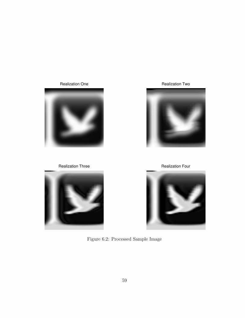
Realization One Realization Two
Realization Three Realization Four
Figure 6.2: Processed Sample Image
59

6.2 Filters of Varying Sizes
Once the filter function correctness is confirmed, more filters of varying sizes can be con-structed to observe the trend in performance, logic utilization, and power dissipation. Itshould be noted that the coefficients used to derive the power figures for filters with di-mension larger than 3 × 3 are not derived from a pre-existing or pre-designed filter. Assuch, the power figures should only be considered as a general guideline of what power dis-sipation could look like. For filter dimension less than 3 × 3, the filter coefficients derivedfrom Chapter 3 are truncated.
6.2.1 Performance
Opimitization of signal routing and module placement on FPGA is an intense and laboriousprocess. To assist in the design, tools often provide several optimization settings that cansignificantly affect the performance, logic utilization and the power dissipation of the finaldesign. Since the FPGA hardware is traditionally not optimized for power, the goal for thisresearch is to optimize for maximum performance instead. A list of detailed settings for thesynthesizer and fitter can be found in Appendix B. The maximum operating speed achievedusing these settings is shown in Table 6.1. The maximum operating speed is limited to375.09 MHz by the memory element used to construct the horizontal shift registers (z1).
Table 6.1: Maximum Operating Speed (MHz) for Realization One With and Without DSEOptimization.
Filter Order 1x1 2x2 3x3 4x4 5x5 6x6 7x7Without DSE 375.09 349.55 331.13 301.04 229.04 282.00 252.50
With DSE 375.09 375.09 375.09 375.09 375.09 345.07 329.49
With the aid of the Design Space Explorer (DSE), the performance can be increaseddramatically. DSE is capable of enumerating a list of possible synthesizer/fitter configu-rations that can potentially give a better performance. A list of seed numbers is enteredinto the DSE and the optimization goal can be selected. Since this research is focused onperformance enhancement, searching for the best performance option was selected. Themaximum operating speed for realization one after using DSE is shown in Table 6.1. Asone can see, the performance has improved dramatically and the fmax is close to 375.09MHz for most filter sizes of realization one. The performance eventually deteriorates dueto the increasing size of the design. It is evident that DSE can significantly increase the
60

performance of the design, and as a result, all realizations are DSE-optimized to ensurethe maximum operating frequency is attained.
Table 6.2 shows a summary of the maximum operating speed for realization two, real-ization three, and realization four after DSE optimization has been applied. Realizationone shows the least amount of performance deterioration as the filter order increases. Re-alization four performs better than realization three as filter order increases is no surprise,since realization four is realization three without instantiating the same poles multipletimes. Realization two has the worst performance figure due to its hybrid parallel-cascaderealization, which has a tendency of increasing fan out at the input of the digital filter andthe input of the tree adder. If the intended field of application requires high performance2D digital filter, realization one and realization four are preferred over realization two andrealization three.
Table 6.2: Maximum Operating Speed (MHz) for Realization One, Two, Three and Fourafter Design Space Explorer.
Filter Order 1x1 2x2 3x3 4x4 5x5 6x6 7x7One 375.09 375.09 375.09 375.09 375.09 345.07 329.49Two 375.09 375.09 343.41 306.00 256.61 NA NA
Three 375.09 372.30 362.32 344.47 281.53 NA NAFour 375.09 375.09 375.09 373.83 361.66 NA NA
Operating speed, however, is only a part of the story. Throughput is the better indicatorof performance, which is usually measured in bits per second, as it represents the maximumpossible quantity of data that can be transmitted under ideal circumstances. To calculatethroughput, maximum operating speed is multiplied by cycle time. The theoretical cycletime for each realization is presented in Table 4.1 and is shown again in Table 6.3, combinedwith the actual cycle time assuming tadd is 12, tmult is 10, and tshift is 1.
Table 6.3: Theoretical and Actual Cycle Time for Each RealizationRealization Theoretical cycle time Actual cycle time (clock cycles)
One 2tadd + tmult + 1 2× 12 + 10 + 1 = 35Two 2tadd + tmult + 1 2× 12 + 10 + 1 = 35
Three tadd + tmult + 1 12 + 10 + 1 = 23Four tadd + tmult + 1 12 + 10 + 1 = 23
Multiplying actual cycle time (from Table 6.3) by maximum operating frequency (fromTable 6.2), maximum throughput is obtained in Table 6.4 in terms of million pixels per
61

second. As one can see, even though the maximum operating frequency is roughly thesame across realizations of smaller filter order, the throughput is dramatically differentdue to cycle time. Realization four emerges as the definitive filter if performance is ofmajor concern. Realization three shows promise as a close second to realization one.However, due to decrease in fmax as filter order increases, realization three is not as goodas realization four.
Table 6.4: Throughput (million pixels/second) for Each Realization.Filter Order 1x1 2x2 3x3 4x4 5x5 6x6 7x7
One 10.72 10.72 10.72 10.72 10.72 9.86 9.41Two 10.72 10.72 9.81 8.74 7.33 NA NA
Three 16.31 16.19 15.75 14.98 12.24 NA NAFour 16.31 16.31 16.31 16.25 15.72 NA NA
6.2.2 Logic Utilization
As presented in Chapter 2, the number of processors required for each realization is derivedfrom previous work [9]. The number of processors required for each realization is reiteratedin Table 6.5, where M1, M2, and r are the horizontal dimension, vertical dimension and therank of the matrix B, respectively. To determine the correlation of logic utilization betweenthe realizations and the implementations, the number of processors used to construct eachrealization is translated into the number of combinational ALUTs, logic registers and 18bit DSP multipliers, which is what the Quartus II tool uses when describing the logicutilization of a given implementation.
Table 6.5: Processors Required for Each Realization (does not include the final tree adder).Filter Processors requiredOne (M1 + 1)(M2 + 1) +M1 +M2
Two r(2M1 + 1 + 2M2 + 1)Three 3M1M2 + 2(M1 +M2)Four M1M2 + 2(M1 +M2)
As aforementioned, four modules from the Quartus II Megawizard Library are used toconstruct the filter implementations: FP adders, FP multipliers, horizontal shift registersand vertical shift registers. The corresponding logic utilization required for each module is
62
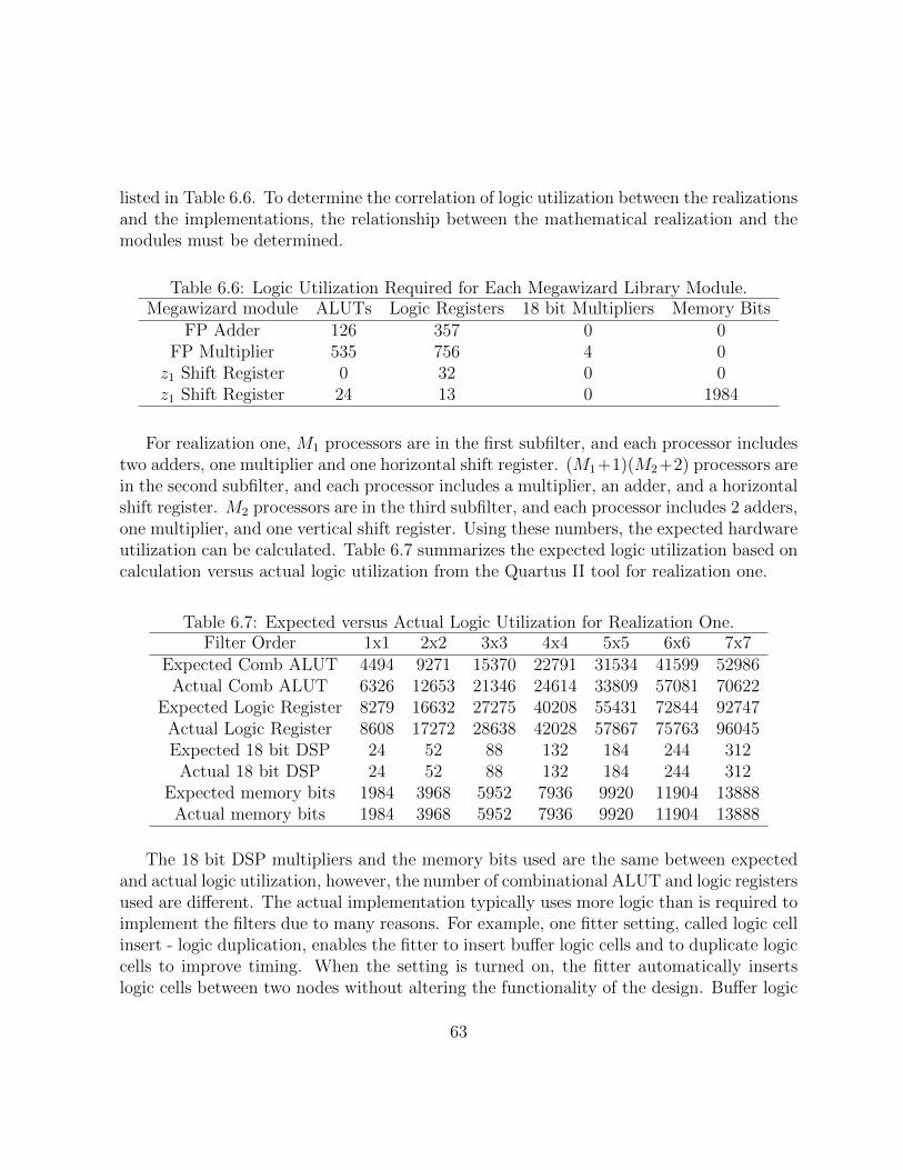
listed in Table 6.6. To determine the correlation of logic utilization between the realizationsand the implementations, the relationship between the mathematical realization and themodules must be determined.
Table 6.6: Logic Utilization Required for Each Megawizard Library Module.Megawizard module ALUTs Logic Registers 18 bit Multipliers Memory Bits
FP Adder 126 357 0 0FP Multiplier 535 756 4 0z1 Shift Register 0 32 0 0z1 Shift Register 24 13 0 1984
For realization one, M1 processors are in the first subfilter, and each processor includestwo adders, one multiplier and one horizontal shift register. (M1+1)(M2+2) processors arein the second subfilter, and each processor includes a multiplier, an adder, and a horizontalshift register. M2 processors are in the third subfilter, and each processor includes 2 adders,one multiplier, and one vertical shift register. Using these numbers, the expected hardwareutilization can be calculated. Table 6.7 summarizes the expected logic utilization based oncalculation versus actual logic utilization from the Quartus II tool for realization one.
Table 6.7: Expected versus Actual Logic Utilization for Realization One.Filter Order 1x1 2x2 3x3 4x4 5x5 6x6 7x7
Expected Comb ALUT 4494 9271 15370 22791 31534 41599 52986Actual Comb ALUT 6326 12653 21346 24614 33809 57081 70622
Expected Logic Register 8279 16632 27275 40208 55431 72844 92747Actual Logic Register 8608 17272 28638 42028 57867 75763 96045Expected 18 bit DSP 24 52 88 132 184 244 312
Actual 18 bit DSP 24 52 88 132 184 244 312Expected memory bits 1984 3968 5952 7936 9920 11904 13888
Actual memory bits 1984 3968 5952 7936 9920 11904 13888
The 18 bit DSP multipliers and the memory bits used are the same between expectedand actual logic utilization, however, the number of combinational ALUT and logic registersused are different. The actual implementation typically uses more logic than is required toimplement the filters due to many reasons. For example, one fitter setting, called logic cellinsert - logic duplication, enables the fitter to insert buffer logic cells and to duplicate logiccells to improve timing. When the setting is turned on, the fitter automatically insertslogic cells between two nodes without altering the functionality of the design. Buffer logic
63

cells are created from unused combinational ALUT and logic registers in the device. Yetanother setting called duplicate logic for fan-out control duplicates logic or registers toimprove fan-out. Duplicating logic or registers can help improve timing in paths wheremoving a register in a failing path to reduce routing delay creates another failing path, orwhere there are timing problems due to high fan-out nodes. A combination of these fittersettings helps to improve the maximum operating frequency of a design at the cost of higherlogic utilization. The same analysis can be applied to other realizations/implementations,but the task would be redundant and is therefore not shown. Instead, the logic utilizationfor all implementations is shown.
Table 6.8: Actual Logic Utilization for Each Realization.Filter Order 1x1 2x2 3x3 4x4 5x5 6x6 7x7
One Comb ALUT 6326 12653 21346 24614 33809 57081 70622Logic Register 8608 17272 28638 42028 57867 75763 96045
18 bit DSP 24 52 88 132 184 224 312Memory bits 1984 3968 5952 7936 9920 11904 13888
Percentage (%) 5 10 17 24 33 46 58Two Comb ALUT 3847 27571 50060 79191 92393 NA NA
Logic Register 6624 35550 65584 104926 123746 NA NA18 bit DSP 24 120 224 360 528 NA NA
Memory bits 9920 17856 31744 49600 103168 NA NAPercentage (%) 4 22 40 63 78 NA NA
Three Comb ALUT 6317 18130 31573 51747 78403 NA NALogic Register 8651 27708 42066 68302 101306 NA NA
18 bit DSP 24 84 136 228 344 NA NAMemory bits 3968 11904 17856 27776 49600 NA NA
Percentage (%) 5 15 25 41 63 NA NAFour Comb ALUT 4667 10730 21052 31967 36164 NA NA
Logic Register 6543 14702 28100 41683 57070 NA NA18 bit DSP 24 84 136 228 344 NA NA
Memory bits 1984 3968 5952 7936 11904 NA NAPercentage (%) 4 9 17 25 34 NA NA
Table 6.8 shows the logic utilization for all implementations of 2D digital filter fordifferent varying sizes. The percentage (%) indicated in the table is the amount of FPGAhardware resource utilizated needed to fit the implementation. As it can be seen, allimplementations have nearly the same logic utilization when the filter size is small. The
64

amount of growth for each implementation is different and there are several reasons thatcan contribute to the growth factor. A fixed amount of circuitry is required to construct thefilter when filter size increases both in the horizontal and vertical direction. This entailsadditional FP multipliers, adders and shift registers are needed. Furthermore, as theamount of circuitry increases, the more difficult it is to meet timing. With aforementionedfitter settings, such as logic cell insert - logic duplication and duplicate logic for fan-outcontrol, timing can be more easily met at the cost of additional logic utilization. As thefilter size increases, these effect are compounded, and eventually contributes to significantincrease in logic utilization.
Overall, both realization one and four are suitable candidates for area reduction. Bothrealizations use roughly the same amount of logic to synthesize and fit the design. If theresearch is to be carried out in standard cell design flow, realization one and realizationfour would be the ideal candidate since smaller logic utilization means less gate count andquicker turn over. Realization two and realization three, however, are terrible candidates.The logic utilization is twice as much or more for realization two and realization three, whencompared to realization one and realization four. In actuality, the problem for realizationtwo and realization three is similar. Both realizations implement the horizontal and verticalpoles multiple time in the filter structure. This occupies a substantial amount of logic andleads to increase in logic utilization.
6.2.3 Power Dissipation
In the world of circuit design, trade offs are common. For FPGA design, this equates totrading power and area for flexibility. This does not always appeal to the ASIC crowdsince area can translate directly to silicon cost and power can translate to heat. As aresult it is unfair to compare the results obtained from FPGA hardware directly to itsASIC counterpart.
Power dissipation is linked directly to the input. Typically there is always a worstcase input vector that will trigger the worst power dissipation. In other words, the powerdissipation is directly related to the input vector. For example, a black image will dissipatesignificantly less power than the sample image, since many of the data paths do not toggle.To figure out the worst power vector, however, would take a long for a complex design.For this research, a 3 × 3 sample impulse response from previous work is presented, and2D digital filter coefficients are derived from various transformation. However, that meansthere will not be enough coefficients for filter larger than 3 × 3. To cope with this problem,coefficients are duplicated in order to have the right number of coefficients. In some cases
65

the output is full of noise, or outright incorrect. Some may argue this produces boguspower data. But one must keep in mind that the work presented in this thesis is on the2D digital filter implementation on FPGA, not the design of 2D digital filter.
Table 6.9: Power Dissipation for each Realization in mW.Filter Order 1x1 2x2 3x3 4x4 5x5 6x6
One Dynamic Power 236.79 513.65 862.10 1195.62 1720.07 2078.07Static Power 2.70 2.67 2.67 2.73 2.73 2.72
Two Dynamic Power 134.73 717.84 1994.19 2671.14 3636.53 NAStatic Power 2.74 2.71 2.70 2.71 2.75 NA
Three Dynamic Power 261.92 793.77 1277.19 1489.56 2298.41 NAStatic Power 2.67 2.69 2.69 2.7 2.71 NA
Four Dynamic Power 187.8 435.11 828.69 1273.94 1729.01 NAStatic Power 2.70 2.70 2.71 2.72 2.73 NA
The dynamic and static power dissipation for all realizations are shown in Table 6.9.The table shows realization one and realizations four are the more suitable candidate forASIC design since they dissipate less power than realization two and realizations three.Typically power correlates very closely with logic utilization and switching frequency.
66

Chapter 7
Conclusions and Future Work
Four 2D separate denominator digital filters implementations are presented in this thesis.Due to timing constraint, optimization to the filter architecture is made by inserting regis-ters in the DSP pipeline. With this change, the digital filter is able to achieve higher max-imum operating speed. A flexible DSP system based on Altera System On ProgrammableChip technology is presented in this thesis. It is used to functionally verify the correctnessof the digital filter. Various synthesizer and fitter settings, such as logic duplication forfan-out control and logic cell insertion - logic duplication, are discussed in detail. DesignSpace Explorer is introduced and used to increase maximum operating frequency further.
7.1 Conclusions
Performance of the digital filter is directly related to the operating frequency and cycle time.With the help of DSE optimization, operating frequency is roughly equal for all realizationsas filter size increases. However, the cycle time for realization three and four is muchsmaller than one and two due to less logic on the critical path. These two factors combinedcontributes to higher throughput for realization three and four. From the experimentalresult presented, realization four is able to achieve the highest throughput of 15.72 millionpixels per second at 361.66 MHz for a filter size of 5 × 5. Realization three is a close secondwith 12.24 million pixels per second at 281.53 MHz. For high performance applications,realization three or realization four is recommended.
A smaller logic utilization translates to small area in ASIC. Since area directly trans-lates to silicon cost, smaller logic utilization is better for low cost production. From the
67
results presented, realization one and realization four occupies 33% and 34 % of the FPGAresources for a 5 × 5 filter, respectively, which uses half as much resources as realizationtwo and realization three. Realization one and realization four are better choice if the goalis to reduce production cost. Logic utilization also directly correlates with dynamic powerdissipation. The results show that realization one and realization four dissipates the lowestamount of dynamic power at 1720.07 mW and 1729.01 mW for a filter size of 5 × 5.
7.2 Future Work
Realization four is the best candidate if the filter is to be implemented in ASIC flow. Ithas excellent performance, occupies lower area and dissipates lower power compared to allother realizations. For more area reduction on the ASIC implementation, floating pointalgorithms could be converted to fixed point algorithms to eliminate hardware complexity.Alternatively, the floating point pipeline can be customized so the denormalization andthe normalization stage of the floating point operator can be eliminated altogether.
The floating point adder speed versus pipeline depth anomaly observed in Figure 5.3should be studied further. Pipelined floating point operators should see a gradual increasein operating speed as pipeline increases. A sudden and large increase in operating speedis unexpected and requires more careful examination.
68

References
[1] Sen M. Kuo and Woon-Seng Gan. Digital Signal Processing - Architecture, Implemen-tation, and Applications. 2004. 1, 45
[2] Qiu-Ting Wang and Ye Bin. A new recognizing and understanding method of mil-itary airfield image based on geometric structure. In Wavelet Analysis and PatternRecognition, 2007. ICWAPR ’07. International Conference on, volume 3, pages 1241–1246, 2-4 2007. 1
[3] B. Lambrigtsen, A. Tanner, T. Gaier, P. Kangaslahti, and S. Brown. Prototyping anew earth observing sensor - geostar. In Aerospace Conference, 2007 IEEE, pages 1–9, 3-10 2007. 1
[4] G. Linan-Cembrano, L. Carranza, C. Rind, A. Zarandy, M. Soininen, andA. Rodriguez-Vazquez. Insect-vision inspired collision warning vision processor forautomobiles. Circuits and Systems Magazine, IEEE, 8(2):6 –24, second 2008. 1
[5] R.W.M. Smith. A generic scaleable image processing architecture for real-time militaryapplications. In High Performance Architectures for Real-Time Image Processing (Ref.No. 1998/197), IEE Colloquium on, pages 3/1 –3/6, 12 1998. 1
[6] Scott Thibault. FPGA vs. DSP design reliability and maintenance. http://www.
altera.com/literature/wp/wp-01023.pdf, 2011. Online; accessed 6-June-2011. 1
[7] K. Sakiyama, P.R. Schaumont, and I.M. Verbauwbede. Finding the best systemdesign flow for a high-speed jpeg encoder. In Design Automation Conference, 2003.Proceedings of the ASP-DAC 2003. Asia and South Pacific, pages 577 – 578, jan. 2003.1
[8] Michael Parker. FPGA vs. DSP design reliability and maintenance. http://www.
altera.com/literature/wp/wp-01023.pdf, 2011. Online; accessed 11-May-2011. 2
69

[9] Mohammed Yahia Dabbagh and Winser E. Alexander. Multiprocessor implementationof 2-D denominator sparable digital filters for real-time processing. IEEE Trans. onAcoustic, Speech and Signal Processing, 37:872 – 881, June 1989. 4, 11, 62
[10] A. N. Venetsanopoulos and B. G. Mertzios. A decomposition theorem and its impli-cations to the design and realization of two-dimensional filters. IEEE Transactionson Acoustics, Speech and Signal Processing, CAS-33:239 – 249, December 1986. 7
[11] H. Andrews and III Patterson, C. Singular value decomposition (svd) image coding.Communications, IEEE Transactions on, 24(4):425 – 432, apr 1976. 8
[12] D. Coltuc and I. Pitas. Jordan decomposition filters. In Circuits and Systems, 1995.ISCAS ’95., 1995 IEEE International Symposium on, volume 3, pages 1896 –1899vol.3, 30 1995. 8
[13] C. Nikias, A. Chrysafis, and A. Venetsanopoulos. The LU decomposition theorem andits implications to the realization of two-dimensional digital filters. Acoustics, Speechand Signal Processing, IEEE Transactions on, 33(3):694 – 711, jun 1985. 8
[14] Tao Lin, Masayuki Kawamata, and Tatsuo Higuchi. Design of 2-d separable-denominator digital filters based on the reduced-dimensional decomposition. IEEETrans. on Circuits and Systems, 34:934 – 941, August 1987. 17
[15] Takao Hinamoto, Toshiaki Takao, and Mitsuji Muneyasu. Synthesis of 2d separable-denominator digital filters with low sensitivity. Journal of the Franklin Institute,329:1063 – 1080, November 1992. 18
[16] Altera Inc. Floating-point compiler: Increase performancewith fewer resources. http://www.altera.com/literature/wp/
wp-01050-Floating-Point-Compiler-Increasing-Performance-With-Fewer-Resources.
pdf, 2007. Online; accessed 6-June-2011. 46
[17] Terasic Inc. Altera DE4 development and education board specifica-tions. http://www.terasic.com.tw/cgi-bin/page/archive.pl?Language=
English&CategoryNo=138&No=501&PartNo=2, 2011. Online; accessed 11-May-2011.49
[18] Altera Inc. Fast passive parallel configuration. http://www.altera.com/support/
devices/configuration/schemes/fast-passive-parallel/cfg-fpp.html, 2011.Online; accessed 10-May-2011. 50
70

[19] Altera Inc. Avalon interface specifications. http://www.altera.com/literature/
manual/mnl_avalon_spec.pdf, 2011. Online; accessed 8-May-2011. 50, 52
71

APPENDICES
72

Appendix A
Detailed filter implementation onFPGA
This section shows the complete and detailed filter realizations including the coefficientsand interconnects for realization one to realization four. The numerical example includedin this research assumes that each dimension, z1 and z2, contains three roots, one realand two complex. αs and βs are used to denote the polynomial coefficients when the twocomplex roots are combined in the z1 and z2 direction, respectively. λ and γ are used torepresent the single real root in the z1 and z2 directions, respectively.
A.1 Realization One
Realization one contains three separate stages. First stage is composed of three subfilters.First subfilter is a 1D IIR filter in the z1 direction. Second subfilter is a bank of 1DFIR filters. Third subfilter is composed of 1D FIR filter in the z2 direction. The filterarchitecture is shown in Figure A.1.
73

2-1
1-1
1-1
1-1
1-1
w(n1,n2)f(n1,n2)
g(n1,n2)
xh1(n1,n2) -α1
-α3xhM1(n1,n2)
b3,0 b1,0b2,0
1-1
-α2
-β3
1-1
1-1
1-1
b3,1 b1,1b2,1
1-1
1-1
1-1
b3,2 b1,2b2,2
1-1
1-1
1-1
b3,3 b1,3b2,3
1-1
2-1
b0,0
b0,1
b0,2
b0,3
-β2
-β1
2-1
1-1
1-1
1-1
1-1
Figure A.1: Realization One
74

A.2 Realization Two
Realization two is a cascade of two filter banks as shown in Figure A.2. The number ofbanks in each subfilter is equivalent to the number of the rank of matrix B.
Z1-1
f(n1,n2)
Z1-1
-β3
Z1-1
Z2-1 Z2
-1 Z2-1
-β2 -β1
Z1-1 Z1
-1 Z1-1
Z2-1 Z2
-1 Z2-1
Z1-1 Z1
-1 Z1-1
Z2-1 Z2
-1 Z2-1
Z1-1 Z1
-1 Z1-1
Z2-1 Z2
-1 Z2-1
+ g(n1,n2)
-β3 -β2 -β1
-β3 -β2 -β1
-β3 -β2 -β1
-α3 -α2 -α1
-α3 -α2 -α1
-α3 -α2 -α1
-α3 -α1
g1,3
-α2
g1,2 g1,1 g1,0
h1,3 h1,2 h1,1 h1,0
h2,3 h2,2 h2,1 h2,0
h3,3 h3,2 h3,1 h3,0
h4,3 h4,2 h4,1 h4,0
g2,3 g2,2 g2,1 g2,0
g3,3 g3,2 g3,1 g3,0
g4,3 g4,2 g4,1 g4,0
Z1-1
Z1-1
Z1-1
Z1-1
Figure A.2: Realization Two
A.3 Realization Three
Realization three is a combination of many parallel stages as shown in Figure A.3 to A.11followed by a tree adder that sums up the intermediate results.
75

Z1-1 Z1-1 Z1-1
f(n1,n2)
k1(n1,n2)B D
Z1-1
-α2 Z1-1 Z1-1
A
C
-β2
-β1
Z2-1
Z2-1
k2(n1,n2)Z1-1
E
-λ1
Z2-1
Z1-1
f(n1,n2)
-γ1
Z1-1
f(n1,n2)
-γ1Z1-1
G
Z1-1
F
-β2
-β1
Z2-1
Z2-1
k3(n1,n2)
Z1-1
f(n1,n2)
Z1-1
-α2
Z1-1 Z1-1
H
-α1
Ik4(n1,n2)
-λ1
Z2-1
-α1
Figure A.3: Realization Three Subfilter One
Z1-1 Z1-1 Z1-1
f(n1,n2)
k1(n1,n2)B D
Z1-1
-α2 Z1-1 Z1-1
A
C
-β2
-β1
Z2-1
Z2-1
k2(n1,n2)Z1-1
E
-λ1
Z2-1
f(n1,n2)
Z1-1
f(n1,n2)
-γ1Z1-1
G
Z1-1
F
-β2
-β1
Z2-1
Z2-1
k3(n1,n2)
Z1-1
f(n1,n2)
Z1-1
-α2
Z1-1 Z1-1
H
-α1
Ik4(n1,n2)
-λ1
Z2-1
-α1
Figure A.4: Realization Three Subfilter Two
Z1-1 Z1-1 Z1-1
f(n1,n2)
k1(n1,n2)B D
Z1-1
-α2 Z1-1 Z1-1
A
C
-β2
-β1
Z2-1
Z2-1
k2(n1,n2)Z1-1
E
-λ1
Z2-1
Z1-1
f(n1,n2)
-γ1
Z1-1
f(n1,n2)
-γ1Z1-1
G
Z1-1
F
-β2
-β1
Z2-1
Z2-1
k3(n1,n2)
Z1-1
f(n1,n2)
Z1-1
-α2
Z1-1 Z1-1
H
-α1
Ik4(n1,n2)
-λ1
Z2-1
-α1
Figure A.5: Realization Three SubfilterThree
Z1-1 Z1-1 Z1-1
f(n1,n2)
k1(n1,n2)B D
Z1-1
-α2
Z1-1 Z1-1
A C
-β2
-β1
Z2-1
Z2-1
k2(n1,n2)Z1-1
E
-λ1
Z2-1
Z1-1
f(n1,n2)
-γ1
Z1-1
f(n1,n2)
-γ1Z1-1
G
Z1-1
F
-β2
-β1
Z2-1
Z2-1
k3(n1,n2)
Z1-1
f(n1,n2)
Z1-1
-α2
Z1-1 Z1-1
H
-α1
Ik4(n1,n2)
-λ1
Z2-1
-α1
Figure A.6: Realization Three Subfilter Four
Z1-1
f(n1,n2)
Z1-1
-α2
Z1-1 Z1-1
K
-α1
L
Z1-1
J
Z1-1
f(n1,n2)
-γ1
K7(n1,n2)
-λ1
Z2-1
Z1-1
M
k5(n1,n2) k6(n1,n2)
Z1-1
O
Z1-1
N
f(n1,n2)
f(n1,n2)
-β2
-β1
Z2-1
Z2-1
k8(n1,n2)
Z1-1
P
f(n1,n2)
k9(n1,n2)
Z1-1
Z1-1
Z1-1
Z1-1
Z1-1
Z1-1
Z1-1
Z1-1
Z1-1
Z1-1
g(n1,n2)
K1(n1,n2)
K2(n1,n2)K3(n1,n2)
K4(n1,n2)
K5(n1,n2)
K6(n1,n2)
K7(n1,n2)
K8(n1,n2)
K9(n1,n2)
Figure A.7: Realization Three Subfilter Five
Z1-1
f(n1,n2)
Z1-1
-α2
Z1-1 Z1-1
K
-α1
L
Z1-1
J
Z1-1
f(n1,n2)
-γ1
K7(n1,n2)
-λ1
Z2-1
Z1-1
M
k5(n1,n2) k6(n1,n2)
Z1-1
O
Z1-1
N
f(n1,n2)
f(n1,n2)
-β2
-β1
Z2-1
Z2-1
k8(n1,n2)
Z1-1
P
f(n1,n2)
k9(n1,n2)
Z1-1
Z1-1
Z1-1
Z1-1
Z1-1
Z1-1
Z1-1
Z1-1
Z1-1
Z1-1
g(n1,n2)
K1(n1,n2)
K2(n1,n2)K3(n1,n2)
K4(n1,n2)
K5(n1,n2)
K6(n1,n2)
K7(n1,n2)
K8(n1,n2)
K9(n1,n2)
Figure A.8: Realization Three Subfilter Six
76

Z1-1
f(n1,n2)
Z1-1
-α2
Z1-1 Z1-1
K
-α1
L
Z1-1
J
Z1-1
f(n1,n2)
-γ1
K7(n1,n2)
-λ1
Z2-1
Z1-1
M
k5(n1,n2) k6(n1,n2)
Z1-1
O
Z1-1
N
f(n1,n2)
f(n1,n2)
-β2
-β1
Z2-1
Z2-1
k8(n1,n2)
Z1-1
P
f(n1,n2)
k9(n1,n2)
Z1-1
Z1-1
Z1-1
Z1-1
Z1-1
Z1-1
Z1-1
Z1-1
Z1-1
Z1-1
g(n1,n2)
K1(n1,n2)
K2(n1,n2)K3(n1,n2)
K4(n1,n2)
K5(n1,n2)
K6(n1,n2)
K7(n1,n2)
K8(n1,n2)
K9(n1,n2)Figure A.9: Realization Three Subfilter Seven
Z1-1
f(n1,n2)
Z1-1
-α2
Z1-1 Z1-1
K
-α1
L
Z1-1
J
Z1-1
f(n1,n2)
-γ1
K7(n1,n2)
-λ1
Z2-1
Z1-1
M
k5(n1,n2) k6(n1,n2)
Z1-1
O
Z1-1
N
f(n1,n2)
f(n1,n2)
-β2
-β1
Z2-1
Z2-1
k8(n1,n2)
Z1-1
P
f(n1,n2)
k9(n1,n2)
Z1-1
Z1-1
Z1-1
Z1-1
Z1-1
Z1-1
Z1-1
Z1-1
Z1-1
Z1-1
g(n1,n2)
K1(n1,n2)
K2(n1,n2)K3(n1,n2)
K4(n1,n2)
K5(n1,n2)
K6(n1,n2)
K7(n1,n2)
K8(n1,n2)
K9(n1,n2)
Figure A.10: Realization Three SubfilterEight
Z1-1
f(n1,n2)
Z1-1
-α2
Z1-1 Z1-1
K
-α1
L
Z1-1
J
Z1-1
f(n1,n2)
-γ1
K7(n1,n2)
-λ1
Z2-1
Z1-1
M
k5(n1,n2) k6(n1,n2)
Z1-1
O
Z1-1
N
f(n1,n2)
f(n1,n2)
-β2
-β1
Z2-1
Z2-1
k8(n1,n2)
Z1-1
P
f(n1,n2)
k9(n1,n2)
Z1-1
Z1-1
Z1-1
Z1-1
Z1-1
Z1-1
Z1-1
Z1-1
Z1-1
Z1-1
g(n1,n2)
K1(n1,n2)
K2(n1,n2)K3(n1,n2)
K4(n1,n2)
K5(n1,n2)
K6(n1,n2)
K7(n1,n2)
K8(n1,n2)
K9(n1,n2)
Figure A.11: Realization Three SubfilterNine
77

A.4 Realization Four
Since realization four is a modified version of realization three, many subfilters that wereused in realization three are reused in realization four. The interconnect between thesubfilters are rewired to reduce redundant realization of the same pole. Figure A.12 showsthe subfilter used to realize poles in the z1 direction and Figure A.13 shows the subfilterused to realize the poles in the z2 direction. Figure A.14 to A.17 shows the subfilter usedto realize numerator coefficients A to P.
Z1-1
f(n1,n2)
-γ1
Z1-1
Z1-1
-α2
-α1
Z1-1
P
Z1-1
J
Z1-1 Z1-1
K L
Z1-1
Z1-1
Z1-1
M
Z1-1
E
Z1-1 Z1-1
H I
Z1-1
Z1-1
3 Input Tree adder
3 Input Tree adder
k1(n1,n2)
k2(n1,n2)
k3(n1,n2)
k1(n1,n2)
k2(n1,n2)
m1(n1,n2)
m2(n1,n2)
Figure A.12: Realization Four z1 Roots
-λ1
Z2-1
-β2
-β1
Z2-1
Z2-1
g1(n1,n2)
3 Input Tree adder
Z1-1
Z1-1
g(n1,n2)
m1(n1,n2)
m2(n1,n2)
m3(n1,n2)
m4(n1,n2)
Figure A.13: Realization Four z2 Roots
78

Z1-1
f(n1,n2)
-γ1
Z1-1
Z1-1
-α2
-α1
Z1-1
P
Z1-1
J
Z1-1 Z1-1
K L
Z1-1
Z1-1
Z1-1
M
Z1-1
E
Z1-1 Z1-1
H I
Z1-1
Z1-1
3 Input Tree adder
3 Input Tree adder
k1(n1,n2)
k2(n1,n2)
k3(n1,n2)
k1(n1,n2)
k2(n1,n2)
m1(n1,n2)
m2(n1,n2)
Figure A.14: Realization Four NumeratorCoefficients P, J, K, and L
Z1-1
f(n1,n2)
-γ1
Z1-1
Z1-1
-α2
-α1
Z1-1
P
Z1-1
J
Z1-1 Z1-1
K L
Z1-1
Z1-1
Z1-1
M
Z1-1
E
Z1-1 Z1-1
H I
Z1-1
Z1-1
3 Input Tree adder
3 Input Tree adder
k1(n1,n2)
k2(n1,n2)
k3(n1,n2)
k1(n1,n2)
k2(n1,n2)
m1(n1,n2)
m2(n1,n2)
Figure A.15: Realization Four NumeratorCoefficients M, E, H and I
Z1-1
O
Z1-1
G
Z1-1 Z1
-1
B D
Z1-1
Z1-1
Z1-1
N
Z1-1
F
Z1-1 Z1
-1
A C
Z1-1
Z1-1
3 Input Tree adder
3 Input Tree adder
k3(n1,n2)
m3(n1,n2)
m4(n1,n2)
k3(n1,n2)
Figure A.16: Realization Four NumeratorCoefficients B, D, G and O
Z1-1
O
Z1-1
G
Z1-1 Z1
-1
B D
Z1-1
Z1-1
Z1-1
N
Z1-1
F
Z1-1 Z1
-1
A C
Z1-1
Z1-1
3 Input Tree adder
3 Input Tree adder
k3(n1,n2)
m3(n1,n2)
m4(n1,n2)
k3(n1,n2)
Figure A.17: Realization Four NumeratorCoefficients A, C, F, and N
79

Appendix B
Synthesizer and Fitter Settings forPerformance Optimization
B.1 Synthesizer Settings
Optimization Technique: SpeedTiming-Driven Synthesis: CheckedPower-Up Don’t Care: CheckedPowerPlay power optimization: OffPerform physical synthesis for combinational logic for performance: OnPerform register Duplication for Performance: OnPerform register retiminig for Performance: OnLogic cell insertion - logic duplication: OnPerform WYSIWYG (What You See Is What You Get) primitive resynthesis: OnRestructure multiplexers: OffState machine processing: Auto
B.2 Fitter Settings
Seed number: 1Optimize hold timing: All pathsOptimize multi-corner timing: Checked
80

PowerPlay power optimization: OffFitter Effort: Standard Fit (highest effort)Router timing optimization level: MaximumAuto packed registers: NormalEnable beneficial skew optimization: OnOptimize hold timing: All pathsDuplicate logic for fan out control: Not set
81