Embed Size (px)
Citation preview

A7190 2.4GHz FSK/GFSK High Power Transceiver
May, 2013, Version 0.3 (PRELIMINARY) 1 AMICCOM Electronics Corporation
Document TitleA7190 Data Sheet, 2.4GHz 4Mbps Transceiver with 17 dBm output power.
Revision History
Rev. No. History Issue Date Remark0.1 Initial issue. Mar., 2012 Preliminary0.2 Change Data rate to 2 and 4Mbps
Add register LGC,PTH,MXT.CDPM,MOVS, CDPSAug., 2012 Preliminary
0.3 Modify the descriptions of TWOR_E register May., 2013 Preliminary
Important Notice:
AMICCOM reserves the right to make changes to its products or to discontinue any integrated circuit product or servicewithout notice. AMICCOM integrated circuit products are not designed, intended, authorized, or warranted to besuitable for use in life-support applications, devices or systems or other critical applications. Use of AMICCOM productsin such applications is understood to be fully at the risk of the customer.
AMICCOM C
ONFIDENTIA
L

A71902.4GHz FSK/GFSK High Power Transceiver
May, 2013, Version 0.3 (PRELIMINARY) 2 AMICCOM Electronics Corporation
Table of Contents1. General Description ..................................................................................................................................................... 12. Typical Applications..................................................................................................................................................... 13. Feature ........................................................................................................................................................................ 14. Pin Configurations....................................................................................................................................................... 25. Pin Description (I: input; O: output, I/O: input or output)............................................................................................ 36. Chip Block Diagram..................................................................................................................................................... 47. Absolute Maximum Ratings......................................................................................................................................... 58. Electrical Specification................................................................................................................................................. 69. Control Register........................................................................................................................................................... 8
9.1 Control Register Table......................................................................................................................................... 89.2 Control Register Description..............................................................................................................................12
9.2.1 Mode Register (Address: 00h) ...................................................................................................................129.2.2 Mode Control Register (Address: 01h) ......................................................................................................129.2.3 Calibration Control Register (Address: 02h).............................................................................................139.2.4 FIFO Register I (Address: 03h).................................................................................................................139.2.5 FIFO Register II (Address: 04h) ...............................................................................................................139.2.6 FIFO DATA Register II (Address: 05h) .....................................................................................................149.2.7 ID DATA Register (Address: 06h) .............................................................................................................149.2.8 RC OSC Register I (Address: 07h) ............................................................................................................149.2.9 RC OSC Register II (Address: 08h)...........................................................................................................149.2.10 RC OSC Register III (Address: 09h)........................................................................................................159.2.11 CKO Pin Control Register (Address: 0Ah) ..............................................................................................159.2.12 GIO1 Pin Control Register (Address: 0Bh) .............................................................................................169.2.13 GIO2 Pin Control Register (Address: 0Ch) .............................................................................................179.2.14 Data Rate Clock Register (Address: 0Dh) ...............................................................................................189.2.15 PLL Register I (Address: 0Eh) ................................................................................................................189.2.16 PLL Register II (Address: 0Fh)...............................................................................................................189.2.17 PLL Register III (Address: 10h)..............................................................................................................189.2.18 PLL Register IV (Address: 11h) ..............................................................................................................199.2.19 PLL Register V (Address: 12h)................................................................................................................199.2.20 Channel Group Register I (Address: 13h) ...............................................................................................199.2.21 Channel Group Register II (Address: 14h)..............................................................................................199.2.22 TX Register I (Address: 15h)...................................................................................................................199.2.23 TX Register II (Address: 16h) .................................................................................................................209.2.24 Delay Register I (Address: 17h) ..............................................................................................................209.2.25 Delay Register II (Address: 18h).............................................................................................................219.2.26 RX Register (Address: 19h).....................................................................................................................219.2.26 RX Gain Register I (Address: 1Ah) .........................................................................................................229.2.27 RX Gain Register II (Address: 1Bh) ........................................................................................................229.2.28 RX Gain Register III (Address: 1Ch).......................................................................................................229.2.29 RX Gain Register IV (Address: 1Dh).......................................................................................................239.2.30 RSSI Threshold Register (Address: 1Eh) ................................................................................................239.2.31 ADC Control Register (Address: 1Fh) .....................................................................................................239.2.32 Code Register I (Address: 20h)................................................................................................................249.2.33 Code Register II (Address: 21h) ..............................................................................................................249.2.34 Code Register III (Address: 22h).............................................................................................................259.2.35 IF Calibration Register I (Address: 23h).................................................................................................259.2.36 IF Calibration Register II (Address: 24h) ...............................................................................................259.2.37 VCO Current Calibration Register (Address: 25h)..................................................................................259.2.38 VCO Bank Calibration Register I (Address: 26h)....................................................................................269.2.39 VCO Bank Calibration Register II (Address: 27h) ..................................................................................269.2.40 VCO Deviation Calibration Register I (Address: 28h).............................................................................27
AMICCOM C
ONFIDENTIA
L

A71902.4GHz FSK/GFSK High Power Transceiver
May, 2013, Version 0.3 (PRELIMINARY) 3 AMICCOM Electronics Corporation
9.2.41 VCO Deviation Calibration Register II (Address: 29h) ...........................................................................279.2.42.0 DASP0 (Address: 2Ah)(AGT[3:0]=0, page 0) ........................................................................................279.2.42.1 DASP1 (Address: 2Ah) (AGT[3:0]=1, page 1) .......................................................................................289.2.42.2 DASP2 (Address: 2Ah) (AGT[3:0]=2, page 2) .......................................................................................289.2.42.3 DASP3 (Address: 2Ah) (AGT[3:0]=3, page 3) .......................................................................................289.2.42.4 DASP4 (Address: 2Ah) (AGT[3:0]=4, page 4) .......................................................................................289.2.42.5 DASP5 (Address: 2Ah) (AGT[3:0]=5, page 5) .......................................................................................289.2.42.6 DASP6 (Address: 2Ah) (AGT[3:0]=6, page 6) .......................................................................................299.2.42.7 DASP7 (Address: 2Ah) (AGT[3:0]=7, page 7) .......................................................................................299.2.42.8 DASP8 (Address: 2Ah) (AGT[3:0]=8, page 8) .......................................................................................299.2.42.9 DASP9 (Address: 2Ah) (AGT[3:0]=9, page 9) .......................................................................................299.2.42.9 DASP10 (Address: 2Ah) (AGT[3:0]=10, page 10)..................................................................................309.2.43 VCO Modulation Delay Register (Address: 2Bh) ....................................................................................309.2.44 Battery Detect Register (Address: 2Ch) ..................................................................................................309.2.45 TX Test Register (Address: 2Dh).............................................................................................................309.2.46 RX DEM Test Register I (Address: 2Eh) .................................................................................................319.2.47 RX DEM Test Register II (Address: 2Fh) ................................................................................................319.2.48 Charge Pump Current Register I (Address: 30h) ....................................................................................319.2.49 Charge Pump Current Register II (Address: 31h)...................................................................................329.2.50 Crystal Test Register (Address: 32h).......................................................................................................329.2.51 PLL Test Register (Address: 33h)............................................................................................................329.2.52 VCO Test Register (Address: 34h)...........................................................................................................339.2.53 RF Analog Test Register (Address: 35h)..................................................................................................339.2.54 Key data Register (Address: 36h)............................................................................................................349.2.55 Channel Select Register (Address: 37h) ..................................................................................................349.2.56.0 ROMP0 (Address: 38h)(AGT[3:0]=0, page 0)........................................................................................349.2.56.1 ROMP1 (Address: 38h)(AGT[3:0]=1, page 1)........................................................................................349.2.56.2 ROMP2 (Address: 38h)(AGT[3:0]=2, page 2)........................................................................................349.2.56.3 ROMP3 (Address: 38h)(AGT[3:0]=3, page 3)........................................................................................359.2.56.4 ROMP4 (Address: 38h)(AGT[3:0]=4, page 4)........................................................................................359.2.57 Data Rate Clock Register (Address: 39h) ................................................................................................359.2.58 FCR Register (Address: 3Ah) ..................................................................................................................359.2.59 ARD Register (Address: 3Bh)..................................................................................................................369.2.60 AFEP Register (Address: 3Ch) ................................................................................................................369.2.61 FCB Register (Address: 3Dh)..................................................................................................................369.2.61 KEYC Register (Address: 3Eh) ...............................................................................................................379.2.62 USID Register (Address: 3Fh) ................................................................................................................37
10. SPI ............................................................................................................................................................................3810.1 SPI Format.......................................................................................................................................................3910.2 SPI Timing Characteristic................................................................................................................................3910.3 SPI Timing Chart .............................................................................................................................................40
10.3.1 Timing Chart of 3-wire SPI.....................................................................................................................4010.3.2 Timing Chart of 4-wire SPI.....................................................................................................................40
10.4 Strobe Commands ............................................................................................................................................4110.4.1 Strobe Command - Sleep Mode ...............................................................................................................4110.4.2 Strobe Command - ldle Mode..................................................................................................................4110.4.3 Strobe Command - Standby Mode...........................................................................................................4210.4.4 Strobe Command - PLL Mode.................................................................................................................4210.4.5 Strobe Command - RX Mode...................................................................................................................4310.4.6 Strobe Command - TX Mode...................................................................................................................4310.4.7 Strobe Command – FIFO Write Pointer Reset........................................................................................4410.4.8 Strobe Command – FIFO Read Pointer Reset.........................................................................................4410.4.9 Strobe Command – Deep Sleep Mode .....................................................................................................44
10.5 Reset Command ...............................................................................................................................................4510.6 ID Accessing Command ....................................................................................................................................45
10.6.1 ID Write Command.................................................................................................................................4510.6.2 ID Read Command..................................................................................................................................46
AMICCOM C
ONFIDENTIA
L

A71902.4GHz FSK/GFSK High Power Transceiver
May, 2013, Version 0.3 (PRELIMINARY) 4 AMICCOM Electronics Corporation
10.7 FIFO Accessing Command................................................................................................................................4610.7.1 TX FIFO Write Command.......................................................................................................................4610.7.2 Rx FIFO Read Command........................................................................................................................47
11. State machine............................................................................................................................................................4811.1 Key states .........................................................................................................................................................4811.2 FIFO mode........................................................................................................................................................4911.3 Direct mode ......................................................................................................................................................50
12. Crystal Oscillator......................................................................................................................................................5312.1 Use External Crystal........................................................................................................................................5312.2 Use External Clock...........................................................................................................................................53
13. System Clock.............................................................................................................................................................5413.1 Data Rate Setting (4Mbps) ...............................................................................................................................5413.2 Data Rate Setting (2Mbps) ...............................................................................................................................55
14. Transceiver LO Frequency ........................................................................................................................................5614.1 LO Frequency Setting ......................................................................................................................................5614.2 IF Side Band Select ..........................................................................................................................................57
14.2.1 Auto IF Exchange ...................................................................................................................................5714.2.2 Fast Exchange ........................................................................................................................................58
14.3 Auto Frequency Compensation.........................................................................................................................5915. Calibration ................................................................................................................................................................60
15.1 Calibration Procedure ......................................................................................................................................6016. FIFO (First In First Out) ..........................................................................................................................................60
16.1 TX Packet Format in FIFO mode .....................................................................................................................6016.1.1 Basic FIFO mode ....................................................................................................................................6016.1.2 Advanced FIFO mode..............................................................................................................................6116.1.3 Multi-CRC FIFO mode ...........................................................................................................................62
16.2 Bit Stream Process in FIFO mode ....................................................................................................................6416.3 Transmission Time ...........................................................................................................................................6516.4 Usage of TX and RX FIFO................................................................................................................................65
16.4.1 Easy FIFO ..............................................................................................................................................6516.4.2 Segment FIFO ........................................................................................................................................66
17. ADC (Analog to Digital Converter)............................................................................................................................6817.1 RSSI Measurement ..........................................................................................................................................68
18. Battery Detect...........................................................................................................................................................7019. Auto-ack and auto-resend..........................................................................................................................................71
19.1 Basic FIFO plus auto-ack auto-resend .............................................................................................................7119.2 Advanced FIFO plus auto-ack and auto-resend................................................................................................7119.3 WTR Behavior during auto-ack and auto-resend..............................................................................................7219.6 Examples of auto-ack and auto-resend.............................................................................................................74
20. RC Oscillator.............................................................................................................................................................7620.1 WOR Function..................................................................................................................................................7620.2 TWOR Function................................................................................................................................................77
21. AES128 Security Packet............................................................................................................................................7722. Application circuit .....................................................................................................................................................7923. Abbreviations ............................................................................................................................................................8024. Ordering Information................................................................................................................................................8025. Package Information.................................................................................................................................................8126. Top Marking Information..........................................................................................................................................8227. Reflow Profile............................................................................................................................................................8328. Tape Reel Information...............................................................................................................................................8429. Product Status ..........................................................................................................................................................85
AMICCOM C
ONFIDENTIA
L

A7190 2.4GHz FSK/GFSK High Power Transceiver
May, 2013, Version 0.3 (PRELIMINARY) 1 AMICCOM Electronics Corporation
1. General Description
A7190 is a high TX power and low cost 2.4GHz ISM band transceiver. This device integrates both high sensitivityreceiver (-85dBm @4Mbps) and programmable high efficiency power amplifier (15 ~ 17dBm). Based on Data RateRegister (0x0E), user can configure on-air data rates to either 2Mbps or 4Mbps.
A7190 supports fast PLL settling time (30 us) for frequency hopping system. For packet handling, A7190 has built-inseparated (512 bytes) TX/RX FIFO for data buffering and burst transmission, auto-ack and auto-resend, CRC for errorpacket filtering, FEC (7,4 hamming code) for 1-bit data correction per code word, RSSI for clear channel assessment,thermal sensor to monitor relative temperature, WOR (Wake on RX) function to support periodically wake up from sleepmode to RX mode and listen for incoming packets without MCU interaction, data whitening for data encryption /decryption. In addition, A7190 has built-in AES128 co-processor (Advanced Encryption Standard) for advanced dataencryption or decryption which consists of the transformation of a 128-bit block into an encrypted 128-bit block. Thosefunctions are very easy to use while developing a wireless system. All features are integrated in a small QFN 4X4 20pins package.
A7190’s control registers are accessed via 3-wire or 4-wire SPI interface such as TX/RF FIFO, ID register, RSSI value,frequency hopping and calibration procedures. Another one is the unique Strobe command via SPI to control powersaving mode (sleep, idle, standby), TX mode and RX mode. The other connections between A7190 and MCU are GIO1and GIO2 (multi-function GPIO) to output A7190’s status so that MCU could use either polling or interrupt scheme forradio control. Overall, it is very easy to develop a wireless application by a MCU and A7190 because of its rich andeasy-to-use features.
2. Typical Applications
2.4GHz video baby monitor2.4GHz video streamingHiFi quality wireless audio streaming
2400 ~ 2483.5 MHz ISM systemWireless sensors and building automationLong range wireless toys
3. FeatureSmall size (QFN4 X4, 24 pins).Frequency band: 2400 ~ 2483.5MHz.FSK or GFSK modulation.Sleep current (1.5 uA).RX current consumption: 30mA (AGC on).TX current consumption: 107mA (17 dBm)On chip regulator, support input voltage 2.0 ~ 3.6 V.Programmable data rate 2M or 4Mbps.Programmable TX power level from 15 dBm to 17 dBm.High RX sensitivity:
-85dBm at 4Mbps on-air data rate.Fast PLL settling time (30 us) for frequency hopping system.On chip low power RC oscillator for WOR (Wake on RX) function.Built-in AES128 co-processorAGC (Auto Gain Control) for wide RSSI dynamic range.AFC (Auto Frequency Compensation) for frequency drift due to temperature.Support low cost crystal (16 / 18 MHz).Low Battery Detector indication.Easy to use.
Support 3-wire or 4-wire SPI.Unique Strobe command via SPI.ONE register setting for new channel frequency.CRC Error Packet Filtering.
AMICCOM C
ONFIDENTIA
L

A71902.4GHz FSK/GFSK High Power Transceiver
May, 2013, Version 0.3 (PRELIMINARY) 2 AMICCOM Electronics Corporation
Auto-acknowledgement and auto-resend.Separated 512Byte TX/RX FIFO.8-bits RSSI measurement for clear channel indication.Auto Calibrations.Auto IF function.FEC by (7, 4) Hamming code (1 bit error correction / code word).Easy FIFO / Segment FIFO.Support FIFO mode frame sync to MCU.Support direct mode with recovery clock output to MCU.
4. Pin Configurations
VD
D_A
RF
P
RF
N
23 22 21 20 19
7 8 9 10 11
BP
_BG
BP
_RS
SI
CK
O
XO
VD
D_P
LL
RT
C_X
I
RE
GI
VD
D_D
12
24
RT
C_X
O
Fig 4-1. A7190 QFN 4x4 24L Package Top View
AMICCOM C
ONFIDENTIA
L

A7190 2.4GHz FSK/GFSK High Power Transceiver
May, 2013, Version 0.3 (PRELIMINARY) 3 AMICCOM Electronics Corporation
5. Pin Description (I: input; O: output, I/O: input or output)
Pin No. Symbol I/O Function Description1 GND G Ground.2 VDD_PA I PA supply voltage input.3 GND G Ground.4 VDD_VCO I VCO supply voltage input.5 LPF O PLL loop filter output. Connect to loop filter.6 XI I Crystal oscillator input.7 XO O Crystal oscillator output.8 VDD_PLL O PLL supply voltage output. Connect to bypass capacitor.9 REGI I Regulator input. Connect to VDD supply.
10 VDD_D O Digital supply voltage output. Connect to bypass capacitor.11 RTCXI I RTC crystal oscillator input.12 RTCXO O RTC crystal oscillator output.13 SCS DI SPI chip select input.14 SCK DI SPI clock input.15 SDIO DI/O SPI data IO.16 GIO1 DI/O Multi-function IO 1.17 VDD_D O Digital supply voltage output. Connect to bypass capacitor.18 GIO2 DI/O Multi-function IO 2.19 CKO DO Multi-function clock output.20 BP_RSSI O RSSI bypass. Connect to bypass capacitor.21 BP_BG O Band-gap bypass. Connect to bypass capacitor.22 VDD_A O Analog supply voltage output. Connect to bypass capacitor.23 RFP IO Positive RF IO. Connect to balun.24 RFN IO Negative RF IO. Connect to balun.
Back side plate GGround.Back side plate shall be well-solder to ground; otherwise, it will impact RFperformance.
AMICCOM C
ONFIDENTIA
L

A71902.4GHz FSK/GFSK High Power Transceiver
May, 2013, Version 0.3 (PRELIMINARY) 4 AMICCOM Electronics Corporation
6. Chip Block Diagram
Fig 6-1. A7190 Block Diagram
AMICCOM C
ONFIDENTIA
L

A7190 2.4GHz FSK/GFSK High Power Transceiver
May, 2013, Version 0.3 (PRELIMINARY) 5 AMICCOM Electronics Corporation
7. Absolute Maximum Ratings
Parameter With respect to Rating UnitSupply voltage range (VDD) GND -0.3 ~ 3.6 VDigital IO pins range GND -0.3 ~ VDD+0.3 VVoltage on the analog pins range GND -0.3 ~ 2.1 VInput RF level 15 dBmStorage Temperature range -55 ~ 125 C
HBM ± 2K* VESD RatingMM ± 100 V
*Stresses above those listed under “Absolute Maximum Rating” may cause permanent damage to the device. These arestress ratings only; functional operation of the device at these or any other conditions above those indicated in theoperational sections of this specification is not implied. Exposure to absolute-maximum-rated conditions for extendedperiods may affect device reliability.
*Device is ESD sensitive. Use appropriate ESD precautions. HBM (Human Body Mode) is tested under MIL-STD-883FMethod 3015.7. MM (Machine Mode) is tested under JEDEC EIA/JESD22-A115-A.*Device is Moisture Sensitivity Level III (MSL 3).* RFP, RFN and VDD_PA pin are HBM ± 1500V
AMICCOM C
ONFIDENTIA
L

A7190 2.4GHz FSK/GFSK High Power Transceiver
May, 2013, Version 0.3 (PRELIMINARY) 6 AMICCOM Electronics Corporation
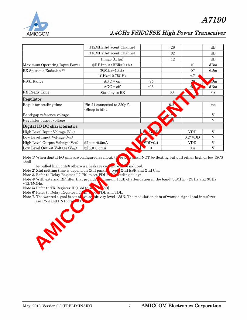
8. Electrical Specification(Ta=25℃, VDD=3.3V, FXTAL =16MHz, with Matching, Balun and low pass filter, On Chip Regulator = 1.8V, unless otherwise noted.)
Parameter Description Min. Type Max. UnitGeneral
Operating Temperature -40 85 ℃
Supply Voltage (VDD) with internal regulator 2.0 2.5 2.7 VVDD_PA 2.0 2.5 2.7 V
Sleep mode (WOR off) *1 2 uASleep mode (WOR on) *1 5 uAIdle Mode (Regulator on) *1 0.3 mAStandby Mode(XOSC on, CLK Gen. on)
5 mA
PLL mode 15 mARX Mode (4Mbps / AGC on) 32 mA
Current Consumption
TX Mode / 17dBm(TBC = 0, TDC = 0, TXC = 2)
107 mA
PLL blockCrystal start up time*2 Idle to standby (Xtal, 49US
type, is stable at 40ppm)0.6 ms
Crystal frequency Data rate: 4M 16 MHzCrystal tolerance Data rate: 4M ±50 ppmCrystal ESR 80 ohmVCO Operation Frequency 2400 2483.5 MHzPLL settling time*3 Loop filter based on app. circuit.
(Standby to PLL)30 us
TransmitterOutput power range 15 17 dBm
30MHz~1GHz -36 dBm1GHz~12.75GHz -30 dBm1.8GHz~ 1.9GHz -47 dBm
Out Band Spurious Emission *4
(PA = 17 dBm)
5.15GHz~ 5.3GHz -47 dBmFrequency deviation*5 Data rate 4Mbps ±1M HzData rate 2 4 MbpsTX ready time*6 Standby to TX 60 usReceiverReceiver sensitivity@ BER = 0.1%
Data rate 4Mbps -85 dBm
IFS = [11], 4Mbps 5MIF Filter bandwidthIFS = [01], 2Mbps 2.5M
Hz
IFS = [11], 4Mbps 4M HzIF center frequencyIFS = [01], 2Mbps 2M Hz
Co-Channel (C/I0) 11 dB±4MHz Adjacent Channel 4 dB
Interference *7
(4Mbps , IF = 4MHz)±8MHz Adjacent Channel - 18 dB
AMICCOM C
ONFIDENTIA
L
A71902.4GHz FSK/GFSK High Power Transceiver
May, 2013, Version 0.3 (PRELIMINARY) 7 AMICCOM Electronics Corporation
±12MHz Adjacent Channel - 28 dB±16MHz Adjacent Channel - 32 dB
Image (C/IIM) - 12 dBMaximum Operating Input Power @RF input (BER=0.1%) 10 dBm
30MHz~1GHz -57 dBmRX Spurious Emission *4
1GHz~12.75GHz -47AGC = on -95 -20 dBmRSSI RangeAGC = off -95 -55 dBm
RX Ready Time Standby to RX 60 us
RegulatorRegulator settling time Pin 21 connected to 330pF.
(Sleep to idle).0.2 ms
Band-gap reference voltage 1.24 VRegulator output voltage 1.8 VDigital IO DC characteristicsHigh Level Input Voltage (VIH) 0.8*VDD VDD VLow Level Input Voltage (VIL) 0 0.2*VDD VHigh Level Output Voltage (VOH) @IOH= -0.5mA VDD-0.4 VDD VLow Level Output Voltage (VOL) @IOL= 0.5mA 0 0.4 V
Note 1: When digital I/O pins are configured as input, those pins shall NOT be floating but pull either high or low (SCSshall be pulled high only); otherwise, leakage current will be induced.Note 2: Xtal settling time is depend on Xtal package type, Xtal ESR and Xtal Cm.Note 3: Refer to Delay Register I (17h) to set PDL (PLL settling delay).Note 4: With external RF filter that provides minimum 17dB of attenuation in the band: 30MHz ~ 2GHz and 3GHz~12.75GHz.Note 5: Refer to TX Register II (16h) to set FD [7:0].Note 6: Refer to Delay Register I (17h) to set PDL and TDL.Note 7: The wanted signal is set above sensitivity level +3dB. The modulation data of wanted signal and interferer are PN9 and PN15, respectively.
AMICCOM C
ONFIDENTIA
L

A7190 2.4GHz FSK/GFSK High Power Transceiver
May, 2013, Version 0.3 (PRELIMINARY) 8 AMICCOM Electronics Corporation
9. Control Register
A7190 has totally built-in 64 control registers that cover all radio control. MCU can access those control registers via3-wire or 4-wire SPI (Support max. SPI data rate up to 10 Mbps). User can refer to chapter 10 for details of SPI interface.A7190 is simply controlled by registers and outputs its status to MCU by GIO1 and GIO2 pins.
9.1 Control Register TableAddress /
Name R/W Bit 7 Bit 6 Bit 5 Bit 4 Bit 3 Bit 2 Bit 1 Bit 0
W RESETN RESETN RESETN RESETN RESETN RESETN RESETN RESETN00hMode R HECF FECF CRCF CER XER PLLER TRSR TRER
W DDPC ARSSI AIF DFCD WORE FMT FMS ADCM01hMode control R DDPC ARSSI AIF CD WORE FMT FMS ADCM
02hCalc R/W - - RCC VCC VBC VDC FBC RSSC
W FEP7 FEP6 FEP5 FEP4 FEP3 FEP2 FEP1 FEP003hFIFO I R LENF7 LENF6 LEN5 LENF4 LENF3 LENF2 LENF1 LENF0
W FPM1 FPM0 PSA5 PSA4 PSA3 PSA2 PSA1 PSA004hFIFO II R FIFOPT7 FIFOPT6 FIFOPT5 FIFOPT4 FIFOPT3 FIFOPT2 FIFOPT1 FIFOPT0
05hFIFO Data R/W FIFO7 FIFO6 FIFO5 FIFO4 FIFO3 FIFO2 FIFO1 FIFO0
06hID Data R/W SYNC7 SYNC6 SYNC5 SYNC4 SYNC3 SYNC2 SYNC1 SYNC0
W WOR_SL7 WOR_SL6 WOR_SL5 WOR_SL4 WOR_SL3 WOR_SL2 WOR_SL1 WOR_SL007hRC OSC I R RCOC7 RCOC6 RCOC5 RCOC4 RCOC3 RCOC2 RCOC1 RCOC0
08hRC OSC II W WOR_SL9 WOR_SL8 WOR_AC5 WOR_AC4 WOR_AC3 WOR_AC2 WOR_AC1 WOR_AC0
W RTCS MRONS INCM ROS RONC RCOSC_E TSEL TWOR_E09hRC OSC III R -- -- -- -- RCBNK3 RCBNK2 RCBNK1 RCBNK0
0AhCKO Pin W ECKOE CKOS3 CKOS2 CKOS1 CKOS0 CKOI CKOE SCKI
0BhGIO1 Pin I W VKM VPM GIO1S3 GIOS2 GIO1S1 GIO1S0 GIO1I GIO1OE
0ChGIO2 Pin II W BBCKS1 BBCKS0 GIO2S3 GIO2S2 GIO2S1 GIO2S0 GIO2I GIO2OE
W CGC1 CGC0 GRC3 GRC2 GRC1 GRC0 CGS XS0DhData Rate Clock R IFS1 IFS0 GRC3 GRC2 GRC1 GRC0 -- -
0EhPLL I R/W CHN7 CHN6 CHN5 CHN4 CHN3 CHN2 CHN1 CHN0
W -- RRC1 RRC0 CHR3 CHR2 CHR1 CHR0 IP80FhPLL II R -- RRC1 RRC0 CHR3 CHR2 CHR1 CHR0 BIP8
W BIP7 BIP6 BIP5 BIP4 BIP3 BIP2 BIP1 BIP010hPLL III R IP7 IP6 IP5 IP4 IP3 IP2 IP1 IP0
W BFP15 BFP14 BFP13 BFP12 BFP11 BFP10 BFP9 BFP811hPLL IV R FSYN-FP1
5 AC14 AC13 AC12 AC11 AC10 AC9 AC8
W BFP7 BFP6 BFP5 BFP4 BFP3 BFP2 BFP1 BFP012hPLL V R AC7 AC6 AC5 AC4 AC3 AC2 AC1 AC0
13hChannel Group I R/W CHGL7 CHGL6 CHGL5 CHGL4 CHGL3 CHGL2 CHGL1 CHGL0
14hChannel Group II R/W CHGH7 CHGH6 CHGH5 CHGH4 CHGH3 CHGH2 CHGH1 CHGH0
15hTX I W GDR GF TMDE TXDI TME FDP2 FDP1 FDP0
AMICCOM C
ONFIDENTIA
L

A71902.4GHz FSK/GFSK High Power Transceiver
May, 2013, Version 0.3 (PRELIMINARY) 9 AMICCOM Electronics Corporation
16hTX II W FD7 FD6 FD5 FD4 FD3 FD2 FD1 FD0
17hDelay I W DPR2 DPR1 DPR0 TDL1 TDL0 PDL2 PDL1 PDL0
18hDelay II W WSEL2 WSEL1 WSEL0 RSSC_D1 RSSC_D0 RS_DLY2 RS_DLY1 RS_DLY0
19hRX W -- AGCE RXSM1 RXSM0 AFC RXDI DMG ULS
1AhRX Gain I R/W MIM IGC1 IGC0 MGC1 MGC0 LGC2 LGC1 LGC0
W RSAGC1 RSAGC0 VTL2 VTL1 VTL0 VTH2 VTH1 VTH01BhRX Gain II R RH7 RH6 RH5 RH4 RH3 RH2 RH1 RH0
W MSC RDU IFS1 IFS0 RSM1 RSM0 ERSSM RSS1ChRX Gain III R RL7 RL6 RL5 RL4 RL3 RL2 RL1 RL0
1DhRX Gain IV W LIMC IFBC1 IFBC0 IFAS MHC1 MHC0 LHC1 LHC0
W RTH7 RTH6 RTH5 RTH4 RTH3 RTH2 RTH1 RTH01EhRSSI Threshold R ADC7 ADC6 ADC5 ADC4 ADC3 ADC2 ADC1 ADC0
W AVSEL1 AVSEL0 MVSEL1 MVSEL0 RADC FSARS XADS CDM1FhADC Control R SNF7 SNF6 SNF5 SNF4 SNF3 SNF2 SNF1 SNF0
W MCS WHTS FECS CRCS IDL1 IDL0 EPML1 EPML020hCode I R SNF15 SNF14 SNF13 SNF12 SNF11 SNF10 SNF9 SNF8
W MSCRC EDRL HECS ETH2 ETH1 ETH0 PTH1 PTH021hCode II R MTCRCF7 MTCRCF6 MTCRCF5 MTCRCF4 MTCRCF3 MTCRCF2 MTCRCF1 MTCRCF0
W CRCINV WS6 WS5 WS4 WS3 WS2 WS1 WS022hCode III R MTCRCF1
5MTCRCF14
MTCRCF13
MTCRCF12
MTCRCF11
MTCRCF10
MTCRCF9 MTCRCF8
W HFR CKGS1 CKGS0 MFBS MFB3 MFB2 MFB1 MFB023hIF Calibration I R - - - FBCF FB3 FB2 FB1 FB0
W PDNTXS RAMPS2 RAMPS1 RAMPS0 DTDS3 DTDS2 DTDS1 DTDS024hIF Calibration II R -- -- -- FCD4 FCD3 FCD2 FCD1 FCD0
W ROSCS -- VCRLS MVCS VCOC3 VCOC2 VCOC1 VCOC025hVCO currentCalibration R - - - VCCF VCB3 VCB2 VCB1 VCB0
W DCD1 DCD0 DAGS CWS MVBS MVB2 MVB1 MVB026hVCO band
Calibration I R - - - - VBCF VB2 VB1 VB0
W MDAG7 MDAG6 MDAG5 MDAG4 MDAG3 MDAG2 MDAG1 MDAG027hVCO band
Calibration II R ADAG7 ADAG6 ADAG5 ADAG4 ADAG3 ADAG2 ADAG1 ADAG0
W DEVS3 DEVS2 DEVS1 DEVS0 DAMR_M VMTE_M VMS_M MSEL28hVCO deviationCalibration I R DEVA7 DEVA6 DEVA5 DEVA4 DEVA3 DEVA2 DEVA1 DEVA0
W MVDS MDEV6 MDEV5 MDEV4 MDEV3 MDEV2 MDEV1 MDEV029hVCO deviationCalibration II R ADEV7 ADEV6 ADEV5 ADEV4 ADEV3 ADEV2 ADEV1 ADEV0
2AhDAS_P0 W QLIM PRS INTRC
(CSXTL5) CSXTL4 CSXTL3 CSXTL2 CSXTL1 CSXTL0
2AhDAS_P1 W -- CELS -- RGC1 RGC0 VRPL1 VRPL0 INTPRC
2AhDAS_P2 W VTRB3 VTRB2 VTRB1 VTRB0 VMRB3 VMRB2 VMRB1 VMRB0
AMICCOM C
ONFIDENTIA
L

A71902.4GHz FSK/GFSK High Power Transceiver
May, 2013, Version 0.3 (PRELIMINARY) 10 AMICCOM Electronics Corporation
2AhDAS_P3 W DCV7 DCV6 DCV5 DCV4 DCV3 DCV2 DCV1 DCV0
W VMG7 VMG6 VMG5 VMG4 VMG3 VMG2 VMG1 VMG02AhDAS_P4 R VMG7 VMG6 VMG5 VMG4 VMG3 VMG2 VMG1 VMG0
2AhDAS_P5 -- -- PKT1 PKT0 PKS PKIS1 PKIS0 IFPK
2AhDAS_P6 -- HPLS HRS PACTL IWS CNT MXD LXD
2AhDAS_P7 XDS VRSEL MS MSCL4 MSCL3 MCSL2 MCSL1 MSCL0
2AhDAS_P8 W RCDL[2] RCDL[1] RCDL[0] MBK MBNK[3] MBNK[2] MBNK[1] MBNK[0]
2AhDAS_P9 W MRCOC[7] MRCOC[6] MRCOC[5] MRCOC[4] MRCOC[3] MRCOC[2] MRCOC[1] MRCOC[0]
2AhDAS_P10 W MTCRCS DRS -- -- -- -- SPL1 SPL0
2BhVCO modulation
DelayW DMV1 DMV0 DEVFD2 DEVFD1 DEVFD0 DEVD2 DEVD1 DEVD0
W -- RGV1 RGV0 QDS BVT2 BVT1 BVT0 BD_E2ChBattery detect R -- RGV1 RGV0 BDF BVT2 BVT1 BVT0 BD_E
2DhTX test W ASMV1 ASMV0 TPC1 TPC0 TDC1 TDC0 TBC1 TBC0
2EhRx DEM test I W DMT DCM1 DCM0 CDPM MXT SLF2 SLF1 SLF0
2FhRx DEM test II W AGCH1 AGCH0 DCL2 DCL1 DCL0 RAW -- MOVS
30hCharge Pump
Current IW CPM3 CPM2 CPM1 CPM0 CPT3 CPT2 CPT1 CPT0
31hCharge Pump
Current IIW CPTX3 CPTX2 CPTX1 CPTX0 CPRX3 CPRX2 CPRX1 CPRX0
32hCrystal test W CDPS CPS CPCH1 CPCH0 CPCS XCC XCP1 XCP0
33hPLL test W MDEN OLM PRIC1 PRIC0 PRRC1 PRRC0 SDPW NSDO
34hVCO test W DEVGD2 DEVGD1 DEVGD0 -- RLB1 RLB0 VBS1 VBS0
35hRF Analog test W AGT3 AGT2 AGT1 AGT0 RFT3 RFT2 RFT1 RFT0
36h Key_data W/R KEY7 KEY6 KEY5 KEY4 KEY3 KEY2 KEY1 KEY0
37hChannel Select W CHI3 CHI2 CHI1 CHI0 CHD3 CHD2 CHD1 CHD0
38hROM_P0 W -- -- MIGS MRGS MRSS MTMS MADS MBGS
W -- -- -- FBG4 FBG3 FBG2 FBG1 FBG038hROM_P1 R -- -- -- FBGR4 FBGR3 FBGR2 FBGR1 FBGR0
W -- -- -- CTR4 CTR3 CTR2 CTR1 CTR038hROM_P2 R -- -- -- CTRR4 CTRR3 CTRR2 CTRR1 CTRR0
W FGC1 FGC0 SRS2 SRS1 SRS0 CRS2 CRS1 CRS038hROM_P3 R -- -- SRSR2 SRSR1 SRSR0 CRSR2 CRSR1 CRSR0
38h W -- STMP STM5 STM4 STM3 STM2 STM1 STM0
AMICCOM C
ONFIDENTIA
L

A71902.4GHz FSK/GFSK High Power Transceiver
May, 2013, Version 0.3 (PRELIMINARY) 11 AMICCOM Electronics Corporation
ROM_P4 R -- STMP STMR5 STMR4 STMR3 STMR2 STMR1 STMR039h
Data Rate CLK W SDR7 SDR6 SDR5 SDR4 SDR3 SDR2 SDR1 SDR0
W FCL1 FCL0 ARC3 ARC2 ARC1 ARC0 EACKS EARTS3AhFCR R ARTEF VPOAK RCR3 RCR2 RCR1 RCR0 EACKS EARTS3BhARD W ARD7 ARD6 ARD5 ARD4 ARD3 ARD2 ARD1 ARD0
W EACKF SPSS ACKFEP5 ACKFEP4 ACKFEP3 ACKFEP2 ACKFEP1 ACKFEP03ChAFEP R -- -- EARTS EARTS EARTS TXSN2 TXSN1 TXSN03DhFCF W/R FCB7 FCB6 FCB5 FCB4 FCB3 FCB2 FCB1 FCB0
3EhKEYCl W KEYOS AFIDS ARTMS MIDS AESS -- AKFS EDCRS
W RND7 RND6 RND5 RND4 RND3 RND2 RND1 RND03FhID code R ICD7 ICD6 ICD5 ICD4 ICD3 ICD2 ICD1 ICD0
Legend: - = unimplemented
AMICCOM C
ONFIDENTIA
L

A7190 2.4GHz FSK/GFSK High Power Transceiver
May, 2013, Version 0.3 (PRELIMINARY) 12 AMICCOM Electronics Corporation
9.2 Control Register Description9.2.1 Mode Register (Address: 00h)
Bit R/W Bit 7 Bit 6 Bit 5 Bit 4 Bit 3 Bit 2 Bit 1 Bit 0R HECF FECF CRCF CER XER PLLER TRSR TRERName W RESETN RESETN RESETN RESETN RESETN RESETN RESETN RESETN
Reset -- -- -- -- -- -- -- --
RESETN: Write to this register by 0x00 to issue reset command, then it is auto clear
HECF: Head Control Flag. (Clear by any Strobe command.)HEC is CRC-8 result from FCB + DFL (refer to chapter 16 for details)[0]: HEC pass. [1]: HEC error.
FECF: FEC flag. (FECF is read clear.)[0]: FEC pass. [1]: FEC error.
CRCF: CRC flag. (CRCF is read clear.)[0]: CRC pass. [1]: CRC error.
CER: RF chip enable Register.[0]: RF chip is disabled. [1]: RF chip is enabled.
XER: Internal crystal oscillator enable Register.[0]: Crystal oscillator is disabled. [1]: Crystal oscillator is enabled.
PLLER: PLL enable Register.[0]: PLL is disabled. [1]: PLL is enabled.
TRSR: TRX Mode Select Register.[0]: RX. [1]: TX. When TRE set, the chip will enter TX or RX mode by TRS register.
TRER: TRX Enable Register.[0]: Disable. [1]: Enable. It will be clear after end of packet encountered in FIFO mode.
9.2.2 Mode Control Register (Address: 01h)Bit R/W Bit 7 Bit 6 Bit 5 Bit 4 Bit 3 Bit 2 Bit 1 Bit 0
R DDPC ARSSI AIF CD WORE FMT FMS ADCMName W DDPC ARSSI AIF DFCD WORE FMT FMS ADCMReset 0 0 0 0 0 0 0 0
DDPC (Direct mode data pin control): Direct mode modem data can be accessed via SDIO pin when this register isenabled.[0]: Disable. [1]: Enable.
ARSSI: Auto RSSI measurement while entering RX mode. Recommend ARSSI = [1].[0]: Disable. [1]: Enable.
AIF (Auto IF Offset): RF LO frequency will auto offset one IF frequency while entering RX mode.[0]: Disable. [1]: Enable.If AIF =1, then,FRXLO = FPLLS - FIF, for up side band (ULS = 0, 19h).FRXLO = FPLLS + FIF, for low side band (ULS = 1, 19h)
CD / DFCD: DFCD: Data Filter by CD.[0]: Disable.[1]: Enable. The data package would be filtered while the input power level is below the threshold level (RTH[7:0], 1Eh).
DFCD (Read only): Carrier detector signal.[0]: Input power below threshold. [1]: Input power above threshold.
WORE: Wireless Wakeup System Enable.[0]: Disable.
AMICCOM C
ONFIDENTIA
L

A71902.4GHz FSK/GFSK High Power Transceiver
May, 2013, Version 0.3 (PRELIMINARY) 13 AMICCOM Electronics Corporation
[1]: Enable. This bit will be clear after wakeup.
FMT: Reserved for internal usage only. Shall be set to [0].
FMS: Direct/FIFO mode select.[0]: Direct mode. [1]: FIFO mode.
ADCM: ADC measurement enable (Auto clear when done).[0]: Disable measurement or measurement finished. [1]: Enable measurement.
ADCM A7190 @ Standby mode A7190 @ RX mode[0] Disable ADC Disable ADC[1] Measure temperature Measure RSSI, carrier detectRefer to chapter 17 for details.
9.2.3 Calibration Control Register (Address: 02h)Bit R/W Bit 7 Bit 6 Bit 5 Bit 4 Bit 3 Bit 2 Bit 1 Bit 0
Name R/W -- -- RCC VCC VBC VDC FBC RSSCReset -- -- 0 0 0 0 0 0
RCC: RC Oscillator calibration enable (Auto clear when done).[0]: Disable. [1]: Enable.
VCC: VCO Current calibration enable (Auto clear when done).[0]: Disable. [1]: Enable .
VBC: VCO Bank calibration enable (Auto clear when done).[0]: Disable. [1]: Enable.
VDC: VCO Deviation calibration enable (Auto clear when done).[0]: Disable. [1]: Enable.
FBC: IF Filter Bank calibration enable (Auto clear when done).[0]: Disable . [1]: Enable.
RSSC: RSSI calibration enable (Auto clear when done).[0]: Disable. [1]: Enable.
9.2.4 FIFO Register I (Address: 03h)Bit R/W Bit 7 Bit 6 Bit 5 Bit 4 Bit 3 Bit 2 Bit 1 Bit 0
Name R -- -- -- -- LENF11 LENF10 LENF9 LENF8W -- -- -- -- FEP11 FEP10 FEP9 FEP8R LENF7 LENF6 LEN5 LENF4 LENF3 LENF2 LENF1 LENF0W FEP7 FEP6 FEP5 FEP4 FEP3 FEP2 FEP1 FEP0
Reset 0 0 1 1 1 1 1 1
FEP [11:0]: FIFO End Pointer for TX FIFO and Rx FIFO.FIFO length = (FEP+1) bytes.Refer to chapter 16 for details.
LENF [11:0]: Received FIFO Length = LENF + 1.Used in dynamic length mode. (EDRL = 1).Refer to chapter 16 for details.
9.2.5 FIFO Register II (Address: 04h)Bit R/W Bit 7 Bit 6 Bit 5 Bit 4 Bit 3 Bit 2 Bit 1 Bit 0
Name R FIFOPT7 FIFOPT6 FIFOPT5 FIFOPT4 FIFOPT3 FIFOPT2 FIFOPT1 FIFOPT0W FPM1 FPM0 PSA5 PSA4 PSA3 PSA2 PSA1 PSA0
Reset 0 1 0 0 0 0 0 0
AMICCOM C
ONFIDENTIA
L

A71902.4GHz FSK/GFSK High Power Transceiver
May, 2013, Version 0.3 (PRELIMINARY) 14 AMICCOM Electronics Corporation
FPM [1:0]: FIFO Pointer Margin[00]: 4 bytes. [01]: 8 bytes. [10]: 12 bytes. [11]: 16 bytes.
PSA [5:0]: Used for Segment FIFO.Refer to chapter 16 for details.
FIFOPT[7:0]: FIFO pointer index (read only).The FIFO access pointer = FIFOPT x 2.
9.2.6 FIFO DATA Register II (Address: 05h)Bit R/W Bit 7 Bit 6 Bit 5 Bit 4 Bit 3 Bit 2 Bit 1 Bit 0
Name R/W FIFO7 FIFO6 FIFO5 FIFO4 FIFO3 FIFO2 FIFO1 FIFO0Reset 0 0 0 0 0 0 0 0
FIFO [7:0]: FIFO data.TX FIFO and RX FIFO share the same address (05h).TX FIFO is max 512-byte write only.RX FIFO is max 512-byte read only.Refer to chapter 16 for details.
9.2.7 ID DATA Register (Address: 06h)Bit R/W Bit 7 Bit 6 Bit 5 Bit 4 Bit 3 Bit 2 Bit 1 Bit 0
Name R/W SYNC7 SYNC6 SYNC5 SYNC4 SYNC3 SYNC2 SYNC1 SYNC0Reset 0 0 0 0 0 0 0 0
ID [7:0]: ID data (sync word, max 8 bytes).When this address is accessed, ID Data is input or output sequential (ID Byte 0,1, 2, 3 …., 7) corresponding to Write orRead.Recommend to set ID Byte 0 = 5xh or Axh.Refer to section 10.6 for details.
9.2.8 RC OSC Register I (Address: 07h)Bit R/W Bit 7 Bit 6 Bit 5 Bit 4 Bit 3 Bit 2 Bit 1 Bit 0
R RCOC7 RCOC6 RCOC5 RCOC4 RCOC3 RCOC2 RCOC1 RCOC0Name W WOR_SL7 WOR_SL6 WOR_SL5 WOR_SL4 WOR_SL3 WOR_SL2 WOR_SL1 WOR_SL0Reset 0 0 0 0 0 0 0 0
RCOC [7:0]: RC Oscillator Calibration Value (read only).
9.2.9 RC OSC Register II (Address: 08h)Bit R/W Bit 7 Bit 6 Bit 5 Bit 4 Bit 3 Bit 2 Bit 1 Bit 0
Name W WOR_SL9 WOR_SL8 WOR_AC5 WOR_AC4 WOR_AC3 WOR_AC2 WOR_AC1 WOR_AC0Reset 0 0 0 0 0 0 1 1
WOR_AC [5:0]: 6-bits WOR Active Timer for TWOR Function
WOR_SL [9:0]: 10-bits WOR Sleep Timer for TWOR Function.WOR_SL [9:0] are from address (07h) and (08h),
Device Active = (WOR_AC+1) x (1/4092), (244us ~ 15.6ms).Device Sleep = (WOR_SL+1) x (1/4092), (7.8ms ~ 7.99s).
AMICCOM C
ONFIDENTIA
L

A71902.4GHz FSK/GFSK High Power Transceiver
May, 2013, Version 0.3 (PRELIMINARY) 15 AMICCOM Electronics Corporation
G IO 1 P in(W T R )
R C O sc.
S ta rt W O R R Xsleep s leep
W O R _S L W O R _ AC
X ta l O sc.
W O R _S L
Refer to chapter 18 for details
9.2.10 RC OSC Register III (Address: 09h)Bit R/W Bit 7 Bit 6 Bit 5 Bit 4 Bit 3 Bit 2 Bit 1 Bit 0
R -- -- -- -- RCBNK3 RCBNK2 RCBNK1 RCBNK0Name W RTCS MRONS INCM ROS RONC RCOSC_E TSEL TWOR_EReset 1 0 0 1 1 0 0 0
RCBNK [3:0]: Ring Osc. calibration bank value.
RTCS: internal Oscillator selection in sleep mode. Recommend RTCS = [0].[0]: RC oscillator. [1]: RTC oscillator.
MRONS: Manual RON value setting.[0]: Auto. [1]: Manual.
INCM: Reserved for internal usage only. It should be set to [0].
ROS: Ring oscillator high current mode select. It should be set to [1].
RONC: RON calibration.[0]: Disable. [1]: Enable.
RCOSC_E: RC Oscillator Enable.[0]: Disable. [1]: Enable.
TSEL: Timer select for TWOR function.[0]: Use WOR_AC. [1]: Use WOR_SL.
TWOR_E: Enable TWOR function.[0]: Disable TWOR function.[1]: Enable TWOR mode. Wake up MCU by a periodic TWOR output.
9.2.11 CKO Pin Control Register (Address: 0Ah)Bit R/W Bit 7 Bit 6 Bit 5 Bit 4 Bit 3 Bit 2 Bit 1 Bit 0
Name W ECKOE CKOS3 CKOS2 CKOS1 CKOS0 CKOI CKOE SCKIReset 1 0 1 1 1 0 1 0
ECKOE: External Clock Output Enable for CKOS [3:0]= [0100] ~ [0111].[0]: Disable. [1]: Enable.
CKOS [3:0]: CKO pin output select.[0000]: DCK (TX data clock).[0001]: RCK (RX recovery clock).[0010]: FPF (FIFO pointer flag).[0011]: Logic OR gate by EOP, EOVBC, EOFBC, EOVCC, EOVDC and RSSC_OK. (Internal usage only).[0100]: FSYCK / 2.[0101]: FSYCK / 4.[0110]: RXD.[0111]: FSYNC..[1000]: WCK.
AMICCOM C
ONFIDENTIA
L

A71902.4GHz FSK/GFSK High Power Transceiver
May, 2013, Version 0.3 (PRELIMINARY) 16 AMICCOM Electronics Corporation
[1001]: PF8M.[1010]: ROSC.[1011]: MXDEC (MXT=1:inverter signal of OKADCN, MXT=0: DEC)[1100]: BDF.[1101]: FSYCK .[1110]: VPOAK[1111]: WRTC.
CKOI: CKO pin output signal invert.[0]: Non-inverted output. [1]: Inverted output.
CKOE: CKO pin Output Enable.[0]: High Z. [1]: Enable.
SCKI: SPI clock input invert.[0]: Non-inverted input. [1]: Inverted input.
9.2.12 GIO1 Pin Control Register (Address: 0Bh)Bit R/W Bit 7 Bit 6 Bit 5 Bit 4 Bit 3 Bit 2 Bit 1 Bit 0
Name W VKM VPM GIO1S3 GIO1S2 GIO1S1 GIO1S0 GIO1I IRQ1OEReset 0 0 0 0 0 0 0 1
VKM: Valid packet mode select.[0]: by event. [1]: by pulse.
VPM: Valid Pulse width select.[0]: 20u. [1]: 40u.
GIO1S [3:0]: GIO1 pin function select.
GIO1S [3:0] TX state RX state[0000] ARCWTR (Wait until TX or RX finished)[0001] EOAC (end of access code) FSYNC[0010] TMEO or TMDEO(TX
modulation enable)CD(carrier detect)
[0011] SID1 Detect Output(ID1DO)[0100] MCU wakeup signal (TWOR)[0101] MTCRCINT /In phase demodulator input(DMII)[0110] SDO ( 4 wires SPI data out)[0111] TRXD In/Out ( Direct mode )[1000] RXD ( Direct mode )[1001] TXD ( Direct mode )[1010] PDN_RX[1011] External FSYNC input in RX direct mode *[1100] MXINC(MXT=1:EOADC.MXT=0:INC.)[1101] FPF[1110] VPOAK (Auto Resend OK Output)[1111] FMTDO (FIFO mode TX Data Output testing)
<Case 1: If IDL = [01], ID = 4-bytes>
AMICCOM C
ONFIDENTIA
L

A71902.4GHz FSK/GFSK High Power Transceiver
May, 2013, Version 0.3 (PRELIMINARY) 17 AMICCOM Electronics Corporation
R X M ode(W T R )
R F S igna l
4-by te s
Pream bleR X D a ta
G IO 1 P in(ID 1D O )
SID 1 Pay load
(F S Y N C )
<Case 2: If IDL = [11], ID = 8-bytes>
R X M ode(W T R )
R F S igna l
4-by te s
Pream bleR X D a ta
G IO 1 P in(ID 1D O )
SID 1 P aylo ad
(F S Y N C )
4 -b ytes
SID 2
GIO1I: GIO1 pin output signal invert.[0]: Non-inverted output. [1]: Inverted output.
GIO1OE: GIO1pin output enable.[0]: High Z. [1]: Enable.
9.2.13 GIO2 Pin Control Register (Address: 0Ch)Bit R/W Bit 7 Bit 6 Bit 5 Bit 4 Bit 3 Bit 2 Bit 1 Bit 0
Name W BBCKS1 BBCKS0 GIO2S3 GIO2S2 GIO2S1 GIO2S0 GIO2I GIO2OEReset 0 1 0 1 0 0 0 1
BBCKS [1:0]: Clock select for digital block. Recommend BBCKS = [00].[00]: FSYCK [01]: FSYCK / 2. [10]: FSYCK / 4. [11]: FSYCK / 8.FSYCK is A7190’s System clock = 16MHz.
GIO2S [3:0]: GIO2 pin function select.
GIO2S [3:0] TX state RX state[0000] WTR (Wait until TX or RX finished)[0001] EOAC (end of access code) FSYNC(frame sync)[0010] TMEO(TX modulation
enable)CD(carrier detect)
[0011] SID1 Detect Output (ID1DO[0100] MCU wakeup signal (TWOR)[0101] MTCRCINT /Quadrature phase demodulator output
(DMIQ).[0110] SDO ( 4 wires SPI data out)[0111] TRXD In/Out ( Direct mode )[1000] RXD ( Direct mode )[1001] TXD ( Direct mode )[1010] PDN_TX[1011] External FSYNC input in RX direct mode *[1100] BDF[1101] FPF[1110] VPOAK (Auto Resend OK Output)
AMICCOM C
ONFIDENTIA
L

A71902.4GHz FSK/GFSK High Power Transceiver
May, 2013, Version 0.3 (PRELIMINARY) 18 AMICCOM Electronics Corporation
[1111] ROMOK(ROM Program OK)If GIO1S=[1011] and direct mode is selected, the internal frame sync function will be disabled. In such case, it isrecommended that user asserts frame sync signal to this input to get better DC estimation of demodulation.
GIO2I: GIO2 pin output signal invert.[0]: Non-inverted output. [1]: Inverted output.
GIO2OE: GIO1pin output enable.[0]: High Z. [1]: Enable.
9.2.14 Data Rate Clock Register (Address: 0Dh)Bit R/W Bit 7 Bit 6 Bit 5 Bit 4 Bit 3 Bit 2 Bit 1 Bit 0
R IFS1 IFS0 GRC3 GRC2 GRC1 GRC0 -- --Name W CGC1 CGC0 GRC3 GRC2 GRC1 GRC0 CGS XSReset 0 0 0 1 1 1 1 1
CGC[1:0]: Clock generation current setting.
GRC [3:0]: Generator Reference Counter.Clock generation reference = FCRYSTAL / (GRC+1). Maximum divide ratio is 16.Refer to chapter 13 for details.
CGS: Clock generator enable. Shall be set to [1].[0]: Disable. [1]: Enable.
XS: Crystal oscillator select. Recommend XS = [1].[0]: Use external clock. [1]: Use external crystal.
9.2.15 PLL Register I (Address: 0Eh)Bit R/W Bit 7 Bit 6 Bit 5 Bit 4 Bit 3 Bit 2 Bit 1 Bit 0
Name R/W CHN7 CHN6 CHN5 CHN4 CHN3 CHN2 CHN1 CHN0Reset 0 0 1 1 1 1 0 0
CHN [7:0]: RF LO Channel number.Refer to chapter 14 for details.
9.2.16 PLL Register II (Address: 0Fh)Bit R/W Bit 7 Bit 6 Bit 5 Bit 4 Bit 3 Bit 2 Bit 1 Bit 0
R -- RRC1 RRC0 CHR3 CHR2 CHR1 CHR0 IP8Name W -- RRC1 RRC0 CHR3 CHR2 CHR1 CHR0 BIP8Reset -- 0 0 0 1 1 1 0
RRC [1:0]: RF PLL reference counter setting.The PLL comparison frequency, FPFD = FCRYSTAL / (RRC+1).
CHR [3:0]: PLL channel step setting. Recommend CHR = [0111]Refer to chapter 14 for details.
9.2.17 PLL Register III (Address: 10h)Bit R/W Bit 7 Bit 6 Bit 5 Bit 4 Bit 3 Bit 2 Bit 1 Bit 0
R IP7 IP6 IP5 IP4 IP3 IP2 IP1 IP0Name W BIP7 BIP6 BIP5 BIP4 BIP3 BIP2 BIP1 BIP0Reset 1 0 0 1 0 1 1 0
BIP [8:0]: (write) LO base frequency integer part setting.BIP [8:0] are from address (0Fh) and (10h),
IP [8:0]: (read) LO frequency integer part value.
AMICCOM C
ONFIDENTIA
L

A71902.4GHz FSK/GFSK High Power Transceiver
May, 2013, Version 0.3 (PRELIMINARY) 19 AMICCOM Electronics Corporation
IP [8:0] are from address (0Fh) and (10h),
Refer to chapter 14 for details.
9.2.18 PLL Register IV (Address: 11h)Bit R/W Bit 7 Bit 6 Bit 5 Bit 4 Bit 3 Bit 2 Bit 1 Bit 0
R FSYN-FP15 AC14 AC13 AC12 AC11 AC10 AC9 AC8Name
W BFP15 BFP14 BFP13 BFP12 BFP11 BFP10 BFP9 BFP8Reset 0 0 0 0 0 0 0 0
9.2.19 PLL Register V (Address: 12h)Bit R/W Bit 7 Bit 6 Bit 5 Bit 4 Bit 3 Bit 2 Bit 1 Bit 0
R AC7 AC6 AC5 AC4 AC3 AC2 AC1 AC0Name W BFP7 BFP6 BFP5 BFP4 BFP3 BFP2 BFP1 BFP0Reset 0 0 0 0 0 1 0 0
BFP [15:0]: LO base frequency fractional part setting. (BFP = [0000] is forbidden.)BFP [15:0] are from address (11h) and (12h),
AC [14:0] (Read): Frequency compensation value if AFC (19h) =1.AC [14:0]: the fractional part in PLL of compensated value if AFC = 1.AFC(19h) RAC [14:0]1 PLLFF [14:0]0 AC [14:0]Refer to chapter 14 for details.
9.2.20 Channel Group Register I (Address: 13h)Bit R/W Bit 7 Bit 6 Bit 5 Bit 4 Bit 3 Bit 2 Bit 1 Bit 0
Name R/W CHGL7 CHGL6 CHGL5 CHGL4 CHGL3 CHGL2 CHGL1 CHGL0Reset 0 0 1 1 1 1 0 0
CHGL [7:0]: PLL channel group low boundary setting. Recommend CHGL = [0x3C].Refer to chapter 15 for details.
9.2.21 Channel Group Register II (Address: 14h)Bit R/W Bit 7 Bit 6 Bit 5 Bit 4 Bit 3 Bit 2 Bit 1 Bit 0
Name R/W CHGH7 CHGH6 CHGH5 CHGH4 CHGH3 CHGH2 CHGH1 CHGH0Reset 0 1 1 1 1 0 0 0
CHGH [7:0]: PLL channel group high boundary setting. Recommend CHGH = [0x78]Refer to chapter 15 for details.
PLL frequency is divided into 3 groups for calibration purpose:Channel
Group1 0 ~ CHGL-1Group2 CHGL ~ CHGH-1Group3 CHGH ~ 255
Note: Each group needs its own VCO current, bank and deviation calibration. Use the same calibration value for thefrequency in the same group.
9.2.22 TX Register I (Address: 15h)Bit R/W Bit 7 Bit 6 Bit 5 Bit 4 Bit 3 Bit 2 Bit 1 Bit 0
Name W GDR GF TMDE TXDI TME FDP2 FDP1 FDP0
AMICCOM C
ONFIDENTIA
L

A71902.4GHz FSK/GFSK High Power Transceiver
May, 2013, Version 0.3 (PRELIMINARY) 20 AMICCOM Electronics Corporation
Reset 0 0 1 0 1 1 1 1
GDR: Gaussian Filter Over-sampling Rate Select.[0]: BT= 0.7[1]: BT= 0.5
GF: Gaussian Filter Select.[0]: Disable. [1]: Enable.
TMDE: TX Modulation Enable for VCO Modulation. Recommend TMDE = [1].[0]: Disable. [1]: Enable.
TXDI: TX data invert. Recommend TXDI = [0].[0]: Non-invert. [1]: Invert.
TME: TX modulation enable. Recommend TME = [1].[0]: Disable. [1]: Enable.
FDP [2:0]: Frequency deviation power setting. Recommend FDP = [111].
9.2.23 TX Register II (Address: 16h)Bit R/W Bit 7 Bit 6 Bit 5 Bit 4 Bit 3 Bit 2 Bit 1 Bit 0
Name W FD7 FD6 FD5 FD4 FD3 FD2 FD1 FD0Reset 0 1 0 0 0 0 0 0
FD [7:0]: TX Frequency Deviation setting.
Formula : FDEV = FPFD /2**16*127*(FD+1)/16 * (FDP+1).
Data Rate FDP[2:0] FD[7:0] Fdev (KHz)4Mbps2Mbps
111110
0x400x40
1000500
9.2.24 Delay Register I (Address: 17h)Bit R/W Bit 7 Bit 6 Bit 5 Bit 4 Bit 3 Bit 2 Bit 1 Bit 0
Name W DPR2 DPR1 DPR0 TDL1 TDL0 PDL2 PDL1 PDL0Reset 0 0 0 1 0 0 0 0
DPR [2:0]: Delay scale. Recommend DPR = [000].
TDL [1:0]: Delay for TRX settling from WPLL to TX/RX.Delay= 20 * (TDL [1:0])*(DPR [2:0]+1) us.
DPR [1:0] TDL [1:0] WPLL to TX Note00 00 0us00 01 20 us00 10 40 us Recommend00 11 60 us
PDL [2:0]: Delay for TX settling from PLL to WPLL.Delay= 10+20 * (PDL [2:0]+1)*(DPR [1:0]+1) us.
DPR [1:0] PDL [2:0] PLL to WPLL(LO freq. fixed)
PLL to WPLL(LO freq changed)
Note
00 001 10 us 50 us Recommend00 010 10 us 70 us00 011 10 us 90 us00 100 10 us 110 us
AMICCOM C
ONFIDENTIA
L

A71902.4GHz FSK/GFSK High Power Transceiver
May, 2013, Version 0.3 (PRELIMINARY) 21 AMICCOM Electronics Corporation
G IO 1 P in(W T R )
R FO P in
T X S tro be
P D L T D L
P a cket (P rea m b le + ID + P ay lo a d)
TX M odePLL M ode
9.2.25 Delay Register II (Address: 18h)Bit R/W Bit 7 Bit 6 Bit 5 Bit 4 Bit 3 Bit 2 Bit 1 Bit 0
Name W WSEL2 WSEL1 WSEL0 RSSC_D1 RSSC_D0 RS_DLY2 RS_DLY1 RS_DLY0Reset 0 1 0 0 0 0 0 1
WSEL [2:0]: XTAL settling delay setting (200us ~ 2.5ms). Recommend WSEL = [010].[000]: 200us. [001]: 400us. [010]: 600us. [011]: 800us.[100]: 1ms. [101]: 1.5ms. [110]: 2ms. [111]: 2.5ms.
G IO 1 P in(W T R )
C rysta lO sc illa to r
PD L TD L
35 0 us W S E LId le
m o deTX o r RX m ode
Pa cket (Pream ble + ID + P aylo ad)R FO P in
RSSC_D [1:0]: RSSI calibration switching time (10us ~ 40us). Recommend RSSC_D = [00].[00]: 10us. [01]: 20us. [10]: 30us. [11]: 40us.
RS_DLY [2:0]: RSSI measurement delay (10us ~ 80us). Recommend RS_DLY = [000].[000]: 10us. [001]: 20us. [010]: 30us. [011]: 40us.[100]: 50us. [101]: 60us. [110]: 70us. [111]: 80us.
9.2.26 RX Register (Address: 19h)Bit R/W Bit 7 Bit 6 Bit 5 Bit 4 Bit 3 Bit 2 Bit 1 Bit 0
Name W MAGC AGCE RXSM1 RXSM0 AFC RXDI DMG ULSReset 0 1 1 0 0 0 0 0
MAGC: Manual AGC control. Recommend MAGC = [0].[0]: auto gain control by AGCE, [1]: manual gain control.
AGCE: Auto Front end Gain Control Select. Recommend AGCE = [1].[0]: Disable. [1]: Enable.
RXSM1: RX clock recovery circuit moving average filter length. Recommend RXSM1 = [1].[0]: 4 bits. [1]: 8 bits.
RXSM0: Demodulator LPF Bandwidth Select. Recommend RXSM0 = [1].[0]: 2MHz. [1]: 1MHz.
AFC: Auto Frequency compensation.[0]: Disable. [1]: Enable.Refer to Ch 14 for details.
AMICCOM C
ONFIDENTIA
L

A71902.4GHz FSK/GFSK High Power Transceiver
May, 2013, Version 0.3 (PRELIMINARY) 22 AMICCOM Electronics Corporation
RXDI: RX data output invert. Recommend RXDI = [0].[0]: Non-inverted output. [1]: Inverted output.
DMG: Demodulator Gain Select. Recommend DMG = [0].[0]: x 1. [1]: x 3.
ULS: RX Up/Low side band select. Recommend ULS = [0].[0]: Up side band, [1]: Low side band.Refer to Ch 14 for details.
9.2.26 RX Gain Register I (Address: 1Ah)Bit R/W Bit 7 Bit 6 Bit 5 Bit 4 Bit 3 Bit 2 Bit 1 Bit 0
Name R/W MIM IGC1 IGC0 MGC1 MGC0 LGC2 LGC1 LGC0Reset 1 1 1 1 1 1 1 1
MIM: Mixer buffer gain setting. Recommend = [1].[0]: 0dB. [1]: -6dB.
IGC [1:0]: IFA Attenuation Select. Recommend IGC = [01].[00]: -12dB. [01]: -6dB. [10]: -2dB. [11]: -0dB.
MGC [1:0]: Mixer Gain Attenuation select. Recommend MGC = [11].[00]: -18dB. [01]: -12dB. [10]: -6dB. [11]: 0dB.
LGC [2:0]: LNA Gain Attenuation select and the range from 3’b000 to 3’b100. Recommend LGC = [100].[000]: -24dB. [001]: -18dB. [010]: -12dB. [011]: -6dB. [100]: 0dB.
9.2.27 RX Gain Register II (Address: 1Bh)Bit R/W Bit 7 Bit 6 Bit 5 Bit 4 Bit 3 Bit 2 Bit 1 Bit 0
R RHC7 RHC6 RHC5 RHC4 RHC3 RHC2 RHC1 RHC0Name W RSAGC1 RSAGC0 VTL2 VTL1 VTL0 VTH2 VTH1 VTH0Reset 1 1 0 0 1 0 0 1
RSAGC [1:0]: AGC clock select. Recommend RSAGC = [11].[00]: 8*FIF . [01]: 4*FIF. [10]: 2*FIF. [11]: FIF.
VTH [2:0] (write): auto gain control high voltage threshold select. Recommend VTH = [011].
VTL [2:0] (write): auto gain control low voltage threshold select. Recommend VTL = [010].
RHC [7:0]: RSSI Calibration High Threshold (read only).
9.2.28 RX Gain Register III (Address: 1Ch)Bit R/W Bit 7 Bit 6 Bit 5 Bit 4 Bit 3 Bit 2 Bit 1 Bit 0
R RLC7 RLC6 RLC5 RLC4 RLC3 RLC2 RLC1 RLC0Name W MSC RDU IFS1 IFS0 RSM1 RSM0 ERSSM RSSReset 1 1 1 1 1 1 0 0
MSC: Mixer AGC switching control. Recommend MSC = [1].
RDU: Manual CGC select.(CGS=1) Recommend RDU = [1].
IFS[1:0]: IF Frequency Select. Recommend IFS = [11].[00]: Reserved. [01]: 2MHz. [10]: Reserved. [11]:4MHZ.
RSM [1:0]: RSSI Margin = RTH – RTL. Recommend RSM = [11].[00]: 5. [01]: 10. [10]: 15. [11]: 20.Refer to chapter 17 for details.
ERSSM: Ending Mode Select in RSSI Measurement. Recommend ERSSM = [0].
AMICCOM C
ONFIDENTIA
L

A71902.4GHz FSK/GFSK High Power Transceiver
May, 2013, Version 0.3 (PRELIMINARY) 23 AMICCOM Electronics Corporation
[0]: RSSI ending by leaving RX. [1]: RSSI ending by Frame SYNC.
RSS: RSSI measurement select.[0]: Disable. [1]: Enable.
RLC [7:0]: RSSI Calibration Low Threshold (read only).
9.2.29 RX Gain Register IV (Address: 1Dh)Bit R/W Bit 7 Bit 6 Bit 5 Bit 4 Bit 3 Bit 2 Bit 1 Bit 0
Name W LIMC IFBC1 IFBC0 IFAS MHC1 MHC0 LHC1 LHC0Reset 1 1 0 0 1 0 1 0
LIMC: IF limiter current select. Recommend LIMC = [1].[0]: 0.3mA. [1]: 0.6mA.
IFBC [1:0]: IF BPF current Select. Recommend IFBC = [10].
IFAS: IF amplifier current setting. Recommend IFAS = [0].
MHC[1:0]: Mixer Current Select. Recommend MHC = [10].[00]: 0.9 mA.. [01]: 1.2 mA. [10]: 1.5 mA. [11]: 1.8 mA.
LHC[1:0]: LNA Current Select. Recommend LHC = [10].[00]: 1mA. [01]: 2mA. [10]: 3mA. [11]: 4mA.
9.2.30 RSSI Threshold Register (Address: 1Eh)Bit R/W Bit 7 Bit 6 Bit 5 Bit 4 Bit 3 Bit 2 Bit 1 Bit 0
R ADC7 ADC6 ADC5 ADC4 ADC3 ADC2 ADC1 ADC0Name W RTH7 RTH6 RTH5 RTH4 RTH3 RTH2 RTH1 RTH0Reset 0 0 0 0 0 0 0 0
ADC [7:0]: ADC output value of thermal sensor and RSSI (read only).ADC input voltage= 0.3 + 1.2 * ADC [7:0] / 256 V.Refer to chapter 17 for details.
RTH [7:0]: Carrier detect threshold.Refer to chapter 17 for details.
CD (Carrier Detect) =1 when RSSI ≧ RTH.CD (Carrier Detect) =0 when RSSI < RTL.
9.2.31 ADC Control Register (Address: 1Fh)Bit R/W Bit 7 Bit 6 Bit 5 Bit 4 Bit 3 Bit 2 Bit 1 Bit 0
Name R SNF7 SNF6 SNF5 SNF4 SNF3 SNF2 SNF1 SNF0W AVSEL1 AVSEL0 MVSEL1 MVSEL0 RADC FSARS XADS CDM
Reset 1 1 1 1 0 0 0 0
AVSEL [1:0]: ADC average times (for Carrier / temperature sensor / external ADC). Recommend AVSEL = [11].[00]: No average. [01]: Average 2 times. [10]: Average 4 times. [11]: Average 8 times.
MVSEL [1:0]: ADC average times (for VCO calibration and RSSI ). Recommend MVSEL = [11].[00]: Average 8 times. [01]: Average 16 times. [10]: Average 32 times. [11]: Average 64 times.
RADC: ADC Read Out Average Mode.[0]: 1, 2, 4, 8 average mode. The average number is according to the setting of AVSEL.[1]: 8, 16, 32, 64 average mode. The average number is according to the setting of MVSEL.
FSARS: ADC Clock Select.[0]: 4MHz. [1]: 8MHz.
AMICCOM C
ONFIDENTIA
L

A71902.4GHz FSK/GFSK High Power Transceiver
May, 2013, Version 0.3 (PRELIMINARY) 24 AMICCOM Electronics Corporation
XADS: External ADC Input Signal Select.[0]: Disable. [1]: Enable.
CDM: RSSI measurement mode. Recommend CDM = [1].[0]: Single mode. [1]: Continuous mode.
SNF [7:0]: Sub-package Flag (read only).Please refer to section 16.1.3
9.2.32 Code Register I (Address: 20h)Bit R/W Bit 7 Bit 6 Bit 5 Bit 4 Bit 3 Bit 2 Bit 1 Bit 0
Name R SNF15 SNF14 SNF13 SNF12 SNF11 SNF10 SNF9 SNF8W MCS WHTS FECS CRCS IDL1 IDL0 EPML1 EPML0
Reset 0 0 0 0 0 1 1 1
MSC: Manchester Enable.[0]: Disable. [1]: Enable.
WHTS: Data Whitening (Data Encryption) Select.[0]: Disable. [1]: Enable (The data is whitening by multiplying PN7).
FECS: FEC Select.[0]: Disable. [1]: Enable (The FEC is (7, 4) Hamming code).
CRCS: CRC Select.[0]: Disable. [1]: Enable. The CRC is set by CRCDNP (0x1A) for either CCITT-16 CRC or CRC-DNP
IDL[1:0]: ID Code Length Select. Recommend IDL= [11].[00]: 2 bytes. [01]: 4 bytes. [10]: 6 bytes. [11]: 8 bytes.4Bytes or 8 Bytes is recommended in A7190 system. If user selects 4Bytes ID code, it is called SID1. If user selects8Bytes ID code, the first 4Bytes ID code is called SID1 and the second 4Bytes ID code is called SID2.
EPML [1:0]: Extend Preamble Length Select. Recommend EPML= [00].[00]: 0 byte. [01]: 1 byte. [10]: 2 bytes. [11]: 4 bytes.
SNF [15:8]: Sub-package Flag (read only).Please refer to section 16.1.3
9.2.33 Code Register II (Address: 21h)Bit R/W Bit 7 Bit 6 Bit 5 Bit 4 Bit 3 Bit 2 Bit 1 Bit 0
Name R MTCRCF7
MTCRCF6
MTCRCF5
MTCRCF4
MTCRCF3
MTCRCF2
MTCRCF1
MTCRCF0
W MSCRC EDRL HECS ETH2 ETH1 ETH0 PTH1 PTH0Reset 0 0 0 0 0 1 1 0
MSCRC: Mask CRC (CRC Data Filtering Enable).[0]: Disable. [1]: Enable.
EDRL: Enable FIFO Dynamic Length[0]: Disable. [1]: Enable.
HECS: Head CRC Select[0]: disable. [1]: enable
ETH [2:0]: Received SID2 Code Error Tolerance. SID2 is only valid if ID length is 8bytes. Recommend ETH = [011].[000]: 0 bit, [001]: 1 bit. [010]: 2 bit. [011]: 3 bit. [100]: 4 bit, [101]: 5 bit. [110]: 6 bit. [111]: 7 bit.
PTH [1:0]: Received SID1 Code Error Tolerance. Recommend PTH = [10].[00]: 0 bit, [01]: 1 bit. [10]: 2 bit. [11]: 3 bit.
MTCRCF [7:0]: Sub-package CRC Flag (read only).
AMICCOM C
ONFIDENTIA
L

A71902.4GHz FSK/GFSK High Power Transceiver
May, 2013, Version 0.3 (PRELIMINARY) 25 AMICCOM Electronics Corporation
Please refer to section 16.1.3
9.2.34 Code Register III (Address: 22h)Bit R/W Bit 7 Bit 6 Bit 5 Bit 4 Bit 3 Bit 2 Bit 1 Bit 0
Name R MTCRCF15
MTCRCF14
MTCRCF13
MTCRCF12
MTCRCF11
MTCRCF10
MTCRCF9 MTCRCF8
W CRCINV WS6 WS5 WS4 WS3 WS2 WS1 WS0Reset 0 0 1 0 1 0 1 0
CRCINV: CRC Inverted Select.[0]: Non-inverted. [1]: inverted.
WS [6:0]: Data Whitening Seed (data encryption key).Refer to chapter 16 for details.
MTCRCF [15:8]: Sub-package CRC Flag (read only).Please refer to section 16.1.3
9.2.35 IF Calibration Register I (Address: 23h)Bit R/W Bit 7 Bit 6 Bit 5 Bit 4 Bit 3 Bit 2 Bit 1 Bit 0
R -- --- --- FBCF FB3 FB2 FB1 FB0Name W HFR CKGS1 CKGS0 MFBS MFB3 MFB2 MFB1 MFB0Reset 1 1 1 0 0 1 1 0
HFR: Helf frequency rate select. Recommend HFR = [1].[0]: 32x. [1]: 16x.
CKGS[1:0]: Clock select. Recommend GKGS = [11].[00]: 1MHz. [01]: 2MHz. [10]: 3MHz. [11]: 4MHz.
FBCF: IF Filter Band Auto Calibration Flag (read only).[0]: Pass. [1]: Fail.
FB [3:0]: IF filter bank (read only).
MFBS: IF Filter Calibration Select. Recommend MFBS = [0].[0]: Auto calibration. [1]: Manual Setting MFB [3:0].
MFB [3:0]: IF Filter Manual Calibration Value. Recommend MFB = [0101].
9.2.36 IF Calibration Register II (Address: 24h)Bit R/W Bit 7 Bit 6 Bit 5 Bit 4 Bit 3 Bit 2 Bit 1 Bit 0
R -- -- -- FCD4 FCD3 FCD2 FCD1 FCD0Name W PDNTXS RAMPS2 RAMPS1 RAMPS0 DTDS3 DTDS2 DTDS1 DTDS0Reset 0 0 0 0 0 0 0 0
PDNTXS: TX Ramp down delay Select.
RAMPS [2:0] : TX Ramp up/down sequence Select. (TBD)[000]: TBC, TDC, TPC [001]: TBC, TPC, TDC [010]: TDC, TBC, TPC [011]: TDC, TPC, TBC [100]: TPC, TBC, TDC[101]: TPC, TDC, TBC [11X]: TBC, TDC, TPC
DTDS[3:0] : Direct mode TX data delay select. (TBD)Delay DTDS[3:0] master clocks.
FCD [4:0]: IF Filter Auto Calibration Deviation from Goal (read only).
9.2.37 VCO Current Calibration Register (Address: 25h)Bit R/W Bit 7 Bit 6 Bit 5 Bit 4 Bit 3 Bit 2 Bit 1 Bit 0
Name R -- -- -- VCCF VCB3 VCB2 VCB1 VCB0
AMICCOM C
ONFIDENTIA
L

A71902.4GHz FSK/GFSK High Power Transceiver
May, 2013, Version 0.3 (PRELIMINARY) 26 AMICCOM Electronics Corporation
W ROSCS -- VCRLS MVCS VCOC3 VCOC2 VCOC1 VCOC0Reset 1 0 0 0 1 1 1 1
ROSCS: Ring oscillator mode selection. Recommend ROSCS = [1].
VCRLS: VCO Current Resistor Select.[0]: low band. [1]: high band.
MVCS: VCO current calibration value select. Recommend MVCS = [1].[0]: Auto. [1]: Manual.
VCOC [3:0]: VCO Current Bank Calibration Value. Recommend VCOC = [1111].MVCS= 1: Manual VCO current bank.
VCCF: VCO Current Auto Calibration Flag (read only).[0]: Pass. [1]: Fail.
VCB [3:0]: VCO Current Bank Calibration Value (read only).MVCS= 0: Auto calibration value (AVCB).MVCS= 1: Manual calibration value (VCOC).
Refer to chapter 15 for details.
9.2.38 VCO Bank Calibration Register I (Address: 26h)Bit R/W Bit 7 Bit 6 Bit 5 Bit 4 Bit 3 Bit 2 Bit 1 Bit 0
R -- -- -- -- VBCF VB2 VB1 VB0Name W DCD1 DCD0 DAGS CWS MVBS MVB2 MVB1 MVB0Reset 1 1 0 1 0 1 0 0
DCD [1:0]: VCO Deviation Calibration Delay. Recommend DCD = [11].Delay time = PDL (Delay Register I, 17h) × ( DCD + 1 ).
DAGS: DAG Calibration Value Select. Recommend DAGS = [0].[0]: Auto calibration value. [1]: Manual calibration value.
CWS: Clock Disable for VCO Modulation. Recommend CWS = [1].[0]: Enable. [1]: Disable.
MVBS: Manual VCO Bank Select. Recommend MVBS = [0].[0]: Auto calibration value(VB[2:0]). [1]: Manual calibration value (MVB[2:0]).
MVB [2:0]: Manual VCO Band. Recommend MVB = [000].VCO frequency increases when MVB increases.
VBCF: VCO Band Auto Calibration Flag (read only).[0]: Pass. [1]: Fail.
VB [2:0]: VCO Bank Calibration Value (read only).MVBS= 0: Auto calibration value (AVB).MVBS= 1: Manual calibration value (MVB).
Refer to chapter 15 for details.
9.2.39 VCO Bank Calibration Register II (Address: 27h)Bit R/W Bit 7 Bit 6 Bit 5 Bit 4 Bit 3 Bit 2 Bit 1 Bit 0
R DAGB7 DAGB6 DAGB5 DAGB4 DAGB3 DAGB2 DAGB1 DAGB0Name W DAGM7 DAGM6 DAGM5 DAGM4 DAGM3 DAGM2 DAGM1 DAGM0Reset 1 0 0 0 0 0 0 0
DAGM [7:0]: DAG Manual Setting Value. Recommend DAGM = [0x80].
DAGB [7:0]: Auto DAG Calibration Value (read only).
AMICCOM C
ONFIDENTIA
L

A71902.4GHz FSK/GFSK High Power Transceiver
May, 2013, Version 0.3 (PRELIMINARY) 27 AMICCOM Electronics Corporation
9.2.40 VCO Deviation Calibration Register I (Address: 28h)Bit R/W Bit 7 Bit 6 Bit 5 Bit 4 Bit 3 Bit 2 Bit 1 Bit 0
R DEVA7 DEVA6 DEVA5 DEVA4 DEVA3 DEVA2 DEVA1 DEVA0Name W DEVS3 DEVS2 DEVS1 DEVS0 DAMR_M VMTE_M VMS_M MSELReset 0 1 1 1 0 0 0 0
DEVA [7:0]: Deviation Output Value.MVDS (29h)= 0: Auto calibration value ((DEVC / 8) × (DEVS + 1)),MVDS (29h)= 1: Manual calibration value (DEVM [6:0]).
DEVS [3:0]: Deviation Output Scaling. Recommend DEVS = [0111].
DAMR_M: DAMR Manual Enable. Recommend DAMR_M = [0].[0]: Disable. [1]: Enable.
VMTE_M: VMT Manual Enable. Recommend VMTE_M = [0].[0]: Disable. [1]: Enable.
VMS_M: VM Manual Enable. Recommend VMS_M = [0].[0]: Disable. [1]: Enable.
MSEL: VMS, VMTE and DAMR control select. Recommend MSEL = [0].[0]: Auto control. [1]: Manual control.
9.2.41 VCO Deviation Calibration Register II (Address: 29h)Bit R/W Bit 7 Bit 6 Bit 5 Bit 4 Bit 3 Bit 2 Bit 1 Bit 0
R DEVC7 DEVC6 DEVC5 DEVC4 DEVC3 DEVC2 DEVC1 DEVC0Name W MVDS DEVM6 DEVM5 DEVM4 DEVM3 DEVM2 DEVM1 DEVM0Reset 0 0 1 1 0 1 1 0
DEVC [7:0]: VCO Deviation Auto Calibration Value (read only).
MVDS: VCO Deviation Calibration Select. Recommend MVDS = [0].[0]: Auto calibration value. [1]: Manual calibration value.
DEVM [6:0]: VCO Deviation Manual Calibration Value. Recommend MVDS = [0x36].
Refer to chapter 15 for details.
9.2.42.0 DASP0 (Address: 2Ah)(AGT[3:0]=0, page 0)Bit R/W Bit 7 Bit 6 Bit 5 Bit 4 Bit 3 Bit 2 Bit 1 Bit 0
Name W QLIM PRS INTXC(CSXTL5) CSXTL4 CSXTL3 CSXTL2 CSXTL1 CSXTL0
Reset 0 0 1 1 1 0 0 0
QLIM: quick charge select for IF limiter amp.[0]: enable. [1]: disable.
PRS: Reserved for internal usage only. It should be set to [0].
INTXC: internal crystal oscillator capacitor selection. Recommend INTXC = [1].[0]: disable. [1]: enable.
CSXTAL[4:0]: On-chip Crystal loading select. Recommend INTXC = [10111] if Xtal Cload = 18pF.CSXTAL is active when INTXC=1 and Each CSXTAL step is 1 pF.CSXTAL is the on-chip capacitor for Xtal oscillator to fine tune offset frequency of the wanted RF carrier.Please refer to chapter 11 or contact AMICCOM’s FAE.
{INTXC,CSXTAL[4:0]} C load (pF)
AMICCOM C
ONFIDENTIA
L

A71902.4GHz FSK/GFSK High Power Transceiver
May, 2013, Version 0.3 (PRELIMINARY) 28 AMICCOM Electronics Corporation
0XXXXX 0100000 16100001 17100010 18
…111110 46111111 47
9.2.42.1 DASP1 (Address: 2Ah) (AGT[3:0]=1, page 1)Bit R/W Bit 7 Bit 6 Bit 5 Bit 4 Bit 3 Bit 2 Bit 1 Bit 0
Name W -- CELS -- RGC1 RGC0 VRPL1 VRPL0 INTPRCReset -- 1 -- 0 0 0 0 1
CELS: Digital voltage select in standby mode. Recommend CELS = [1].
RGC [1:0]: Low power band-gap current select. Recommend RGC = [01]
VRPL [1:0]: internal PLL loop filter resistor value select. Recommend VRPL = [00].[00]: 10Kohm. [01]: 5K ohm. [10]: 3.3 K ohm. [11]: 2.5K ohm.
INTPRC: Internal PLL loop filter resistor and capacitor select. Recommend INTPRC = [1].[0]: disable. [1]: enable
9.2.42.2 DASP2 (Address: 2Ah) (AGT[3:0]=2, page 2)Bit R/W Bit 7 Bit 6 Bit 5 Bit 4 Bit 3 Bit 2 Bit 1 Bit 0
Name W VTRB3 VTRB2 VTRB1 VTRB0 VMRB3 VMRB2 VMRB1 VMRB0Reset 0 0 0 0 0 0 0 0
VTRB [3:0]: Resistor Bank for VT RC Filtering. Shall be set to [1111].
VMRB [3:0]: Resistor Bank for VM RC Filtering. Shall be set to [0000].
9.2.42.3 DASP3 (Address: 2Ah) (AGT[3:0]=3, page 3)Bit R/W Bit 7 Bit 6 Bit 5 Bit 4 Bit 3 Bit 2 Bit 1 Bit 0
Name W DCV7 DCV6 DCV5 DCV4 DCV3 DCV2 DCV1 DCV0Reset 1 0 0 0 0 0 0 0
DCV [7:0]: Demodulator Fix mode DC value. Recommend DCV = [0x80].
9.2.42.4 DASP4 (Address: 2Ah) (AGT[3:0]=4, page 4)Bit R/W Bit 7 Bit 6 Bit 5 Bit 4 Bit 3 Bit 2 Bit 1 Bit 0
Name W VMG7 VMG6 VMG5 VMG4 VMG3 VMG2 VMG1 VMG0Reset 1 0 0 0 0 0 0 0
VMG [7:0]: VM Center Value for Deviation Calibration. Recommend VMG [7:0] = [0x80].
9.2.42.5 DASP5 (Address: 2Ah) (AGT[3:0]=5, page 5)Bit R/W Bit 7 Bit 6 Bit 5 Bit 4 Bit 3 Bit 2 Bit 1 Bit 0
Name W -- -- PKT1 PKT0 PKS PKIS1 PKIS0 IEPKReset -- -- 0 0 1 0 0 0
PKT[1:0]: VCO Peak Detect Current Select. Recommend PKT = [00].
PKS: VCO Current Calibration Mode Select. Recommend PKS = [1].
PKIS[1:0]: AGC Peak Detect Current Select. Recommend PKIS = [00].
IFPK: AGC Amplifier Current Select. Recommend IFPK = [0].
AMICCOM C
ONFIDENTIA
L

A71902.4GHz FSK/GFSK High Power Transceiver
May, 2013, Version 0.3 (PRELIMINARY) 29 AMICCOM Electronics Corporation
9.2.42.6 DASP6 (Address: 2Ah) (AGT[3:0]=6, page 6)Bit R/W Bit 7 Bit 6 Bit 5 Bit 4 Bit 3 Bit 2 Bit 1 Bit 0
Name W -- HPLS HRS PACTL IWS CNT MXD LXDReset -- 0 0 0 0 0 0 0
HPLS: High Power LNA Gain Select. Recommend HPLS = [0].[0]: LGC set to 6dB when in TX Mode. [1]: LGC set to 24dB when in TX Mode.
HRS: Reserved for internal usage only. Shall be set to [0].
PACTL: Reserved for internal usage only. Shall be set to [0].
IWS: Reserved for internal usage only. Shall be set to [0].
CNT: Reserved for internal usage only. Shall be set to [0].
MXD: Reserved for internal usage only. Shall be set to [0].
LXD: Reserved for internal usage only. Shall be set to [0].
9.2.42.7 DASP7 (Address: 2Ah) (AGT[3:0]=7, page 7)Bit R/W Bit 7 Bit 6 Bit 5 Bit 4 Bit 3 Bit 2 Bit 1 Bit 0
Name W XDS VRSEL MS MSCL4 MSCL3 MSCL2 MSCL1 MSCL0Reset 0 0 0 1 0 1 1 0
XDS: VCO Modulation Data Sampling Clock selection. Recommend XDS = [1].[0]: 8x over-sampling Clock. [1]: XCPCK Clock.
VRSEL: AGC Function select. Recommend VRSEL = [0].[0]: RSSI AGC. [1]: Normal AGC.
MS: AGC Manual scale select. Recommend MS = [0].[0]: By (RL−RH). [1]: By MSCL[4:0].
MSCL[4:0]: AGC Manual Scale setting. Recommend MSCL = [00000].
9.2.42.8 DASP8 (Address: 2Ah) (AGT[3:0]=8, page 8)Bit R/W Bit 7 Bit 6 Bit 5 Bit 4 Bit 3 Bit 2 Bit 1 Bit 0
Name W ROBCD2 ROBCD1 ROBCD0 MROBS MROB3 MROB2 MROB1 MROB0Reset 1 0 1 0 1 0 0 0
ROBCD [2:0]: Reserved for internal usage only. It should be set to [000].
MROBS: Manual Ring Osc Bank setting.[0]: Auto. [1]: Manual.
MROB [3:0]: Ring Osc Bank manual calibration value.Manual setting if MROBS =1.
9.2.42.9 DASP9 (Address: 2Ah) (AGT[3:0]=9, page 9)Bit R/W Bit 7 Bit 6 Bit 5 Bit 4 Bit 3 Bit 2 Bit 1 Bit 0
Name W RONCG7 RONCG6 RONCG5 RONCG4 RONCG3 RONCG2 RONCG1 RONCG0Reset 0 1 0 1 0 0 0 0
RONCG [7:0]: N-counter of Ring Osc. Recommend RONCG = [0x3C].N-counter calibration goal or manual setting of Ring Osc.
AMICCOM C
ONFIDENTIA
L

A71902.4GHz FSK/GFSK High Power Transceiver
May, 2013, Version 0.3 (PRELIMINARY) 30 AMICCOM Electronics Corporation
9.2.42.9 DASP10 (Address: 2Ah) (AGT[3:0]=10, page 10)Bit R/W Bit 7 Bit 6 Bit 5 Bit 4 Bit 3 Bit 2 Bit 1 Bit 0
Name W MTCRCS DRS -- -- -- -- SPL1 SPL0Reset 0 0 -- -- -- -- 0 0
MTCRCS: Multi-CRC select.[0]: Disable. [1]: Enable.
DRS: Data received select for MTCRC.[0]: Package will be stored when CRC ok.[1]: Package will be stored when package finish.
SPL: Sub-package length.[00]: 32bytes.[01]: 64bytes.[10]: 128bytes.[11]: 256bytes.
9.2.43 VCO Modulation Delay Register (Address: 2Bh)Bit R/W Bit 7 Bit 6 Bit 5 Bit 4 Bit 3 Bit 2 Bit 1 Bit 0
Name W DMV1 DMV0 DEVFD2 DEVFD1 DEVFD0 DEVD2 DEVD1 DEVD0Reset 1 1 0 0 0 0 1 1
DMV [1:0]: Demodulator D/A Voltage Range Select. Recommend DMV = [11].[00]: 1/32*1.2. [01]: 1/16*1.2. [10]: 1/8*1.2. [11]: 1/4*1.2.
DEVFD [2:0]: VCO Modulation Data Delay by 8x over-sampling Clock. Recommend DEVFD = [111].
DEVD [2:0]: VCO Modulation Data Delay by XCPCK Clock. Recommend DEVD = [111].
9.2.44 Battery Detect Register (Address: 2Ch)Bit R/W Bit 7 Bit 6 Bit 5 Bit 4 Bit 3 Bit 2 Bit 1 Bit 0
R -- RGV1 RGV0 BDF BVT2 BVT1 BVT0 BD_EName W -- RGV1 RGV0 QDS BVT2 BVT1 BVT0 BD_EReset -- 1 1 1 0 0 1 0
RGV [1:0]: Regulator Voltage Select. Recommend RGV = [11].[00]: 2.1V. [01]: 2.0V. [10]: 1.9V. [11]: 1.8V.
BDF : Low Battery Detection Flag (read only).[0]: battery low. [1]: battery high.
QDS: VDD_A Quick Discharge Select. Recommend QDS = [1].[0]: Disable. [1]: Enable.
BVT [2:0]: Battery Voltage Threshold Select.[000]: 2.0V, [001]: 2.1V. [010]: 2.2V. [011]: 2.3V. [100]: 2.4V. [101]: 2.5V. [110]: 2.6V. [111]: 2.7V.
BD_E: Battery Detect Enable.[0]: Disable.[1]: Enable. This bit will be clear after battery detection is triggered.
9.2.45 TX Test Register (Address: 2Dh)Bit R/W Bit 7 Bit 6 Bit 5 Bit 4 Bit 3 Bit 2 Bit 1 Bit 0
Name W ASMV1 ASMV0 TPC1 TPC0 TDC1 TDC0 TBC1 TBC0Reset 1 1 1 1 1 1 1 1
ASMV[1:0]: Ramp up/down clock select. Recommend ASMV = [11].
AMICCOM C
ONFIDENTIA
L

A71902.4GHz FSK/GFSK High Power Transceiver
May, 2013, Version 0.3 (PRELIMINARY) 31 AMICCOM Electronics Corporation
[00]: 8MHz. [01]: 2MHz. [10]: 1MHz. [11]: 0.5MHz.
TPC[1:0]: TX PA Current select.
TDC[1:0]: TX Driver Current select.
TBC[1:0]: TX Buffer Current select.
Refer to A7190 App. Note for more settings.
9.2.46 RX DEM Test Register I (Address: 2Eh)Bit R/W Bit 7 Bit 6 Bit 5 Bit 4 Bit 3 Bit 2 Bit 1 Bit 0
Name W DMT DCM1 DCM0 CDPM MXT SLF2 SLF1 SLF0Reset 0 1 1 0 0 1 1 1
DMT: Reserved for internal usage only. Shall be set to [0].
DCM [1:0]: Demodulator DC estimation mode. Recommend DCM = [10].(The average length before hold is selected by DCL in Code Register II.)[00]: DC set by DCV in 2Fh).[01]: DC holds after SID1detected.[10]: DC holds after FSYNC detected.[11]: No hold.
CDPM: Reset time-out (40bits) counter after SID1 match.[0]: Disable[1]: Enable
MXT: Control the GPIO1 and CKO function (MXDEC,MXINC).[0]: MXDEC=inverter signal of OKADC, MXINC = EOADC[1]: MXDEC = DEC, MXINC = INC
SLF [2:0]: Reserved for internal usage only. Shall be set to [111].
9.2.47 RX DEM Test Register II (Address: 2Fh)Bit R/W Bit 7 Bit 6 Bit 5 Bit 4 Bit 3 Bit 2 Bit 1 Bit 0
Name W AGCH1 AGCH0 DCL2 DCL1 DCL0 RAW -- MOVSReset 1 1 1 1 0 0 -- 0
AGCH[1:0]: AGC Hold mode. Recommend AGCH = [01].[00]: by SID1 detect. [01]: by frame sync (FSYNC) detect.[1x]: no hold
DCL2: DC Estimation Average Length After ID Detected. Recommend DCL2 = [1].[0]: 128 bits. [1]: 256 bits.
DCL[1:0]: DC Estimation Average Length Before ID Detected. Recommend DCL = [10].[00]: 8 bits. [01]: 16 bits. [10]: 32 bits. [11]: 64 bits.
RAW: Raw Data Output Select. Recommend RAW = [1].[0]: latch data output. [1]: RAW data output.
MOVS: Select the moving average data source from the last filter in demodulation.[0]: Select date source from the output of the last filter.[1]: Select date source from the input of the last filter.
9.2.48 Charge Pump Current Register I (Address: 30h)Bit R/W Bit 7 Bit 6 Bit 5 Bit 4 Bit 3 Bit 2 Bit 1 Bit 0
Name W CPM3 CPM2 CPM1 CPM0 CPT3 CPT2 CPT1 CPT0
AMICCOM C
ONFIDENTIA
L

A71902.4GHz FSK/GFSK High Power Transceiver
May, 2013, Version 0.3 (PRELIMINARY) 32 AMICCOM Electronics Corporation
Reset 1 1 1 1 0 0 1 1
CPM [3:0]: Charge Pump Current Setting for VM loop. Recommend CPM = [1111].Charge pump current = (CPM + 1) / 16 mA.
CPT [3:0]: Charge Pump Current Setting for VT loop. Recommend CPT = [0011]. Charge pump current = (CPT + 1) / 16 mA.
9.2.49 Charge Pump Current Register II (Address: 31h)Bit R/W Bit 7 Bit 6 Bit 5 Bit 4 Bit 3 Bit 2 Bit 1 Bit 0
Name W CPTX3 CPTX2 CPTX1 CPTX0 CPRX3 CPRX2 CPRX1 CPRX0Reset 0 0 1 1 0 0 1 1
CPTX [3:0]: Charge Pump Current Setting for TX mode. Recommend CPTX = [0011].Charge pump current = (CPTX + 1) / 16 mA.
CPRX [3:0]: Charge Pump Current Setting for RX mode. Recommend CPRX = [0011]. Charge pump current = (CPRX + 1) / 16 mA.
9.2.50 Crystal Test Register (Address: 32h)Bit R/W Bit 7 Bit 6 Bit 5 Bit 4 Bit 3 Bit 2 Bit 1 Bit 0
Name W CPDS CPS CPCH1 CPCH0 CPCS XCC XCP1 XCP0Reset 0 1 0 0 1 1 0 1
CPDS: Replace the TX carrier by preamble bit (0101…)[0]: TX sends the carrier. [1]: TX sends preamble bits (0101…) to replace carrier.
CPS: PLL charge pump enable. Recommend CPS = [1].[0]: Enable. [1]: Disable.
CPCH[1:0] : Charge Pump High Current. Recommend CHCH = [00]
CPCS : Charge Pump Current Select. Recommend CPCS = [1].[0]: Use CPM for TX, CPT for RX.[1]: Use CPTX for TX, CPRX for RX.
XCC : Crystal Startup Current Selection. Recommend XCC = [1].[0]: about 0.7 mA. [1]: about 1.5 mA.
XCP [1:0]: Crystal Oscillator Regulated Couple Setting. Recommend XCP = [01].[00]: 1.5mA. [01]: 0.5mA. [10]: 0.35mA. [11]: 0.3mA.
9.2.51 PLL Test Register (Address: 33h)Bit R/W Bit 7 Bit 6 Bit 5 Bit 4 Bit 3 Bit 2 Bit 1 Bit 0
Name W MDEN OLM PRIC1 PRIC0 PRRC1 PRRC0 SDPW NSDOReset 0 0 0 1 0 1 0 1
MDEN : Use for Manual VCO Calibration. Shall be set to [0].
OLM : Open Loop Modulation Enable. Shall be set to [0].[0]: Disable. [1]: Enable.
PRIC [1:0]: Prescaler IF Part Current Setting. Shall be set to [01].[00]: 0.95mA. [01]: 1.05mA. [10]: 1.15mA. [11]: 1.25mA.
PRRC [1:0]: Prescaler RF Part Current Setting. Shall be set to [01].[00]: 1.0mA. [01]: 1.2mA. [10]: 1.4mA. [11]: 1.6mA.
SDPW : Clock Delay For Sigma Delta Modulator. Shall be set to [0].[0]: 13 ns. [1]: 26 ns.
NSDO : Sigma Delta Order Setting. Shall be set to [1].
AMICCOM C
ONFIDENTIA
L

A71902.4GHz FSK/GFSK High Power Transceiver
May, 2013, Version 0.3 (PRELIMINARY) 33 AMICCOM Electronics Corporation
[0]: order 2. [1]: order 3.
9.2.52 VCO Test Register (Address: 34h)Bit R/W Bit 7 Bit 6 Bit 5 Bit 4 Bit 3 Bit 2 Bit 1 Bit 0
Name W DEVGD2 DEVGD1 DEVGD0 -- RLB1 RLB0 VBS1 VBS0Reset 0 0 0 -- 1 0 1 1
DEVGD [2:0]: Sigma Delta Modulator Data Delay Setting. Recommend DEVGD = [000].
RLB [1:0]: RF divider Current Select. Shall be set to [10].[00]: 1.2mA. [01]: 1.5mA. [10]: 1.8mA. [11]: 2.1mA.
VBS[1:0] : VCO Buffer Current Setting. Shall be set to [11].
9.2.53 RF Analog Test Register (Address: 35h)Bit R/W Bit 7 Bit 6 Bit 5 Bit 4 Bit 3 Bit 2 Bit 1 Bit 0
Name W AGT3 AGT2 AGT1 AGT0 RFT3 RFT2 RFT1 RFT0Reset 0 0 0 0 0 0 0 0
AGT[3:0]:Page select.AGT[3:0] Address:2Ah Address:38h
0000 DASP0 ROMP00001 DASP1 ROMP10010 DADP2 ROMP20011 DASP3 ROMP30100 DASP4 ROMP40101 DASP5 --0110 DASP6 --0111 DADP7 --1000 DASP8 --1001 DASP9 --1010 DASP10
RFT [2:0]: RF Analog Pin Configuration. Recommend RFT= [000].{XADS, RFT[2:0]} BP_BG BP_RSSI
[0000] Band-gap voltage RSSI voltage[0001] Analog temperature voltage RSSI voltage[0010] Band-gap voltage No connection[0011] Analog temperature voltage No connection[0100] BPF positive in phase output BPF negative in phase output[0101] BPF positive quadrature phase output BPF negative quadrature phase
output[0110] RSSI voltage No connection[0111] RSSI voltage No connection[1000] Band-gap voltage External ADC input source[1001] Analog temperature voltage External ADC input source[1010] Band-gap voltage External ADC input source[1011] Analog temperature voltage External ADC input source[1100] No connection External ADC input source[1101] No connection External ADC input source[1110] No connection External ADC input source[1111] No connection External ADC input source
AMICCOM C
ONFIDENTIA
L

A71902.4GHz FSK/GFSK High Power Transceiver
May, 2013, Version 0.3 (PRELIMINARY) 34 AMICCOM Electronics Corporation
9.2.54 Key data Register (Address: 36h)Bit R/W Bit 7 Bit 6 Bit 5 Bit 4 Bit 3 Bit 2 Bit 1 Bit 0
R KEYO7 KEYO6 KEYO5 KEYO4 KEYO3 KEYO2 KEYO1 KEYO0Name W KEYI7 KEYI6 KEYI5 KEYI4 KEYI3 KEYI2 KEYI1 KEYI0Reset 0 0 0 0 0 0 0 0
KEYI [7:0]: AES128 key input, total 16-btyes. (Write only).
KEYO [7:0]: AES128 key output, total 16-bytes. (Read only). Select by KEYOS (3Eh).
A E S K e y D a t a ( t o t a l 1 6 B y t e s )
K E Y [ 7 : 0 ] K E Y [ 1 5 : 8 ] … K E Y [ 1 2 7 : 1 2 0 ]
9.2.55 Channel Select Register (Address: 37h)Bit R/W Bit 7 Bit 6 Bit 5 Bit 4 Bit 3 Bit 2 Bit 1 Bit 0
Name W CHI3 CHI2 CHI1 CHI0 CHD3 CHD2 CHD1 CHD0
Reset 0 1 1 1 0 1 1 1
CHI [3:0]: Auto IF Offset Channel Number Setting.FCHSP × ( CHI + 1 ) = FIFRefer to chapter 14 for FCHSP setting. Set FCHSP = 500KHz for most of cases.
CHD [3:0]: Channel Frequency Offset for Deviation Calibration.Offset channel number = +/- (CHD + 1).
9.2.56.0 ROMP0 (Address: 38h)(AGT[3:0]=0, page 0)Bit R/W Bit 7 Bit 6 Bit 5 Bit 4 Bit 3 Bit 2 Bit 1 Bit 0
Name W -- -- MIGS MRGS MRSS MTMS MADS MBGSReset 0 0 0 0 0 0 0 0
Reserved for internal usage.
9.2.56.1 ROMP1 (Address: 38h)(AGT[3:0]=1, page 1)Bit R/W Bit 7 Bit 6 Bit 5 Bit 4 Bit 3 Bit 2 Bit 1 Bit 0
W -- -- -- FBG4 FBG3 FBG2 FBG1 FBG0Name R FBGR4 FBGR3 FBGR2 FBGR1 FBGR0Reset 0 0 0 1 0 0 0 0
Reserved for internal usage.
9.2.56.2 ROMP2 (Address: 38h)(AGT[3:0]=2, page 2)Bit R/W Bit 7 Bit 6 Bit 5 Bit 4 Bit 3 Bit 2 Bit 1 Bit 0
W -- -- CTR4 CTR3 CTR2 CTR1 CTR0Name R CTRR4 CTRR3 CTRR2 CTRR1 CTRR0Reset 0 0 0 1 0 0 0 0
Reserved for internal usage. Recommend ROMP2 = [0x30].
AMICCOM C
ONFIDENTIA
L

A71902.4GHz FSK/GFSK High Power Transceiver
May, 2013, Version 0.3 (PRELIMINARY) 35 AMICCOM Electronics Corporation
9.2.56.3 ROMP3 (Address: 38h)(AGT[3:0]=3, page 3)Bit R/W Bit 7 Bit 6 Bit 5 Bit 4 Bit 3 Bit 2 Bit 1 Bit 0
W FGC1 FGC0 SRS2 SRS1 SRS0 CRS2 CRS1 CRS0Name R SRSR2 SRSR1 SRSR0 CRSR2 CRSR1 CRSR0Reset 1 1 1 0 0 1 0 0
Reserved for internal usage.Recommend FGC = [10].Recommend SRS = [100].Recommend CRS = [100].
9.2.56.4 ROMP4 (Address: 38h)(AGT[3:0]=4, page 4)Bit R/W Bit 7 Bit 6 Bit 5 Bit 4 Bit 3 Bit 2 Bit 1 Bit 0
W STMP STM5 STM4 STM3 STM2 STM1 STM0Name R STMP STMR5 STMR5 STMR3 STMR2 STMR1 STMR0Reset 0 0 1 0 0 0 0 0
Reserved for internal usage.
9.2.57 Data Rate Clock Register (Address: 39h)Bit R/W Bit 7 Bit 6 Bit 5 Bit 4 Bit 3 Bit 2 Bit 1 Bit 0
Name W SDR7 SDR6 SDR5 SDR4 SDR3 SDR2 SDR1 SDR0Reset 0 0 0 0 0 0 0 0
SDR [7:0]: Data Rate Setting. On-air Data rate = FIF / (SDR+1).
9.2.58 FCR Register (Address: 3Ah)Bit R/W Bit 7 Bit 6 Bit 5 Bit 4 Bit 3 Bit 2 Bit 1 Bit 0
R ARTEF VPOAK RCR3 RCR2 RCR1 RCR0 EAK EARName W FCL1 FCL0 ARC3 ARC2 ARC1 ARC0 EAK EARReset 0 0 0 1 1 0 0 0
FCL [1:0] : Frame Control Length.[00]: No Frame Control[01]: 1 byte Frame Control. (FCB0), refer to 3Dh and chapter 16 and 20.[10]: 2 byte Frame control. (FCB0+FCB1), refer to 3Dh and chapter 16 and 20.[11]: 4 byte Frame control. (FCB0+FCB1+FCB2+FCB3), refer to 3Dh and chapter 16 and 20.
RCR [3:0]: Decremented ARC[3:0] (read only).
ARC [3:0] : Auto Resend Cycle Setting.[0000]: resend disable.[0001]: 1 [0010]: 2 [0011]: 3 [0100]: 4 [0101]: 5 [0110]: 6 [0111]: 7 [1000]: 8 [1001]: 9 [1010]: 10[1011]: 11 [1100]: 12 [1101]: 13 [1110]: 14 [1111]: 15
EAK : Enable auto-ack.[0]: Disable. [1]: Enable.
EAR : Enable auto-resend.[0]: Disable. [1]: Enable.
ARTEF: Auto re-transmission ending flag (read only).[0]: Resend not end [1]: Finish resend.
VPOAK : Valid Packet or ACK OK Flag. (read only)This bit is clear by any Strobe command.[0]: Neither valid packet nor ACK OK. [1]: Valid packet or ACK OK.
AMICCOM C
ONFIDENTIA
L

A71902.4GHz FSK/GFSK High Power Transceiver
May, 2013, Version 0.3 (PRELIMINARY) 36 AMICCOM Electronics Corporation
Please refer to chapter 16 and 19 for details.
9.2.59 ARD Register (Address: 3Bh)Bit R/W Bit 7 Bit 6 Bit 5 Bit 4 Bit 3 Bit 2 Bit 1 Bit 0
Name W ARD7 ARD6 ARD5 ARD4 ARD3 ARD2 ARD1 ARD0Reset 0 0 0 0 0 0 1 1
ARD[7:0] : Auto Resend DelayARD Delay = 200 us * (ARD+1) (200us ~ 51.2 ms)
[0000-0000]: 200 us.[0000-0001]: 400 us.[0000-0010]: 600 us.…[1111-1111]: 51.2 ms.
Please refer to chapter 19 for details.9.2.60 AFEP Register (Address: 3Ch)
Bit R/W Bit 7 Bit 6 Bit 5 Bit 4 Bit 3 Bit 2 Bit 1 Bit 0Name R - - EARTS2 EARTS1 EARTS0 TXSN2 TXSN1 TXSN0
W EAF SPSS ACKFEP5 ACKFEP4 ACKFEP3 ACKFEP2 ACKFEP1 ACKFEP0Reset 1 1 0 0 0 0 1 1
EAF: Enable ACK FIFO.[0]: Disable. [1]: Enable.
SPSS : Mode Back Select when auto-act and auto-resend are enabled.[0]: Standby mode. [1]: PLL mode.
ACKFEP [5:0]: FIFO Length setting for auto-ack packet.ACK FIFO Length = (ACKFEP[5:0] + 1)max. 64 bytes.
EARTS [2:0]: Enable Auto Resend Read.
TXSN [2:0]: TX Serial Number.This device increases TXSN each time for every new packet and keep the same TXSN when retransmitting.
Please refer to chapter 16 and 19 for details.
9.2.61 FCB Register (Address: 3Dh)Bit R/W Bit 7 Bit 6 Bit 5 Bit 4 Bit 3 Bit 2 Bit 1 Bit 0
Name R/W FCB7 FCB6 FCB5 FCB4 FCB3 FCB2 FCB1 FCB0Reset 0 0 0 0 0 0 0 0
FCB [7:0]: Frame Control Buffer, total 20-bytes.
Please refer to chapter 16 and 19 for details.
Byte Name Bit-Map Description Strobe Cmd0 FCB0 0 0 1 1 1 TXSN2 TXSN1 TXSN0 For auto-resend. NA1 FCB1 [7:0]2 FCB2 [7:0]3 FCB3 [7:0]
ACK infoby user’s attaching
NA
Remark:1. Please refer to section 10.4.10 for details.2. TXSN is auto incremental for every new packet if FCB0 is enabled.
AMICCOM C
ONFIDENTIA
L

A71902.4GHz FSK/GFSK High Power Transceiver
May, 2013, Version 0.3 (PRELIMINARY) 37 AMICCOM Electronics Corporation
3. FCB0 ~ FCB3 is controlled by FCL[1:0] (3Ah)4. User can attach wanted ACK information to FCB1 ~ FCB3 if auto-ack is enabled (EAK =1).
ID c o d eP re a m b le P a y lo a d (C R C )
4 b y te s 4 b y te s 2 b y te sP h y . 6 4 b y te s
F C B
1 ~ 4 b y te s
F E P
8 b its
a u toa c k / re se n d
d y n a m icF IF O
M A C H e a d e r ( s e l f -g e n e ra te d )P H Y H e a d e r ( s e lf - g e n e ra te d )
9.2.61 KEYC Register (Address: 3Eh)Bit R/W Bit 7 Bit 6 Bit 5 Bit 4 Bit 3 Bit 2 Bit 1 Bit 0
Name W KEYOS AFIDS ARTMS MIDS AESS -- AKFS EDCRSReset 0 0 0 0 0 0 0 0
KEYOS: AES128 Key source read select.[0]: If AKFS=1, from RX received encrypted AES128 key data. If AKFS=0, from SPI write AES128 key data.[1]: From encrypted/decrypted AES128 key data.
AFIDS: FIFO ID appendixes select.[0]: Disable. [1]: Enable.
ARTMS: auto-resend duration select.[0]: random interval. [1]: fixed interval.
MIDS: FIFO control byte address mapping for FIFO ID select.[0]: Received device ID. [1]: internal FIFO control byte ID.
AESS: encryption format selection.[1]: Standard AES 128 bit. [0]: proprietary 32 bit.
AKFS: Data packet with decrypted key appendixes select.[0]: Disable. [1]: Enable.
EDRCS: Data encrypt or decrypt select.[0]: Disable. [1]: Enable.
9.2.62 USID Register (Address: 3Fh)Name R/W Bit 7 Bit 6 Bit 5 Bit 4 Bit 3 Bit 2 Bit 1 Bit 0USID W RND7 RND6 RND5 RND4 RND3 RND2 RND1 RND0
RND [7:0]: Random seed for auto-resend interval.
Please refer to chapter 16 and 19 for details.
AMICCOM C
ONFIDENTIA
L

A7190 2.4GHz FSK/GFSK High Power Transceiver
May, 2013, Version 0.3 (PRELIMINARY) 38 AMICCOM Electronics Corporation
10. SPI
A7190 only supports one SPI interface with maximum data rate up to 10Mbps. MCU should assert SCS pin low (SPI chipselect) to active accessing of A7190. Via SPI interface, user can access control registers and issue Strobe command.Figure 10.1 gives an overview of SPI access manners.
3-wire SPI (SCS, SCK and SDIO) or 4-wire SPI (SCS, SCK, SDIO and GIO1/GIO2) configuration is provided. For 3-wireSPI, SDIO pin is configured as bi-direction to be data input and output. For 4-wire SPI, SDIO pin is data input and GIO1(or GIO2) pin is data output. In such case, GIO1S (0bh) or GIO2S (0ch) should be set to [0110].
For SPI write operation, SDIO pin is latched into A7190 at the rising edge of SCK. For SPI read operation, if inputaddress is latched by A7190, data output is aligned at falling edge of SCK. Therefore, MCU can latch data output at therising edge of SCK.
To control A7190’s internal state machine, it is very easy to send Strobe command via SPI interface. The Strobecommand is a unique command set with total 8 commands. See section 10.3, 10.4 and 10.5 for details.
SPI chip select Data In Data Out
3-Wire SPI SCS pin = 0 SDIO pin SDIO pin
4-Wire SPI SCS pin = 0 SDIO pin GIO1 (GIO1S=0110) /GIO2 (GIO2S=0110)
ADDRreg DataByte ADDRreg ADDRreg
ADDRFIFO DataByte0 DataByte1 DataByte2 DataByte3
ADDRID DataByte0 DataByte1 DataByte2 DataByte3
StrobeCommandSleep Mode
Sleep Mode
Read/Write IDregister
Read/Write RFFIFO
Read/Write register
SCS
DataByten
DataByte DataByte
StrobeCommandIdle Mode
Idle Mode
StrobeCommandSTBY Mode
STBY Mode
StrobeCommandPLL Mode
PLL Mode
StrobeCommandRX Mode
RX Mode
StrobeCommandTX Mode
TX Mode
StrobeCommandFIFO Write Reset
FIFO Write Reset
StrobeCommandFIFO Read Reset
FIFO Read Reset
Figure 10.1 SPI Access Manners
AMICCOM C
ONFIDENTIA
L

A71902.4GHz FSK/GFSK High Power Transceiver
May, 2013, Version 0.3 (PRELIMINARY) 39 AMICCOM Electronics Corporation
10.1 SPI FormatThe first bit (A7) is critical to indicate A7190 the following instruction is “Strobe command” or “control register”. SeeTable 10.1 for SPI format. Based on Table 10.1, To access control registers, just set A7=0, then A6 bit is used to indicateread (A6=1) or write operation (A6=0). See Figure 10.2 (3-wire SPI) and Figure 10.3 (4-wire SPI) for details.
Address Byte (8 bits) Data Byte (8 bits)CMD R/W Address DataA7 A6 A5 A4 A3 A2 A1 A0 7 6 5 4 3 2 1 0
Table 10.1 SPI FormatAddress byte:
Bit 7: Command bit[0]: Control registers.[1]: Strobe command.
Bit 6: R/W bit[0]: Write data to control register.[1]: Read data from control register.
Bit [5:0]: Address of control register
Data Byte:Bit [7:0]: SPI input or output data, see Figure 10.2 and Figure 10.3 for details.
10.2 SPI Timing Characteristic
No matter 3-wire or 4-wire SPI interface is configured, the maximum SPI data rate is 10 Mbps. To active SPI interface,SCS pin must be set to low. For correct data latching, user has to take care hold time and setup time between SCK andSDIO. See Table 10.2 for SPI timing characteristic.
Parameter Description Min. Max. UnitTFC Frequency clock *1. 10 MHzTSE Enable setup time. 50 nsTHE Enable hold time. 50 nsTSW TX Data setup time. 50 nsTHW TX Data hold time. 50 nsTDR RX Data delay time. 0 50 ns
Table 10.2 SPI Timing Characteristic
Note 1: SPI frequency clock should be slower than BBCLK(0Ch).
AMICCOM C
ONFIDENTIA
L

A71902.4GHz FSK/GFSK High Power Transceiver
May, 2013, Version 0.3 (PRELIMINARY) 40 AMICCOM Electronics Corporation
10.3 SPI Timing ChartIn this section, 3-wire and 4-wire SPI interface read / write timing are described.
10.3.1 Timing Chart of 3-wire SPI
A7 DW
7A0A1A2A3A4A5A6 DW
0DW
5DW
6 DW
1
SCS
SCK
SDIO
SCK
SCS
A7 DR7A0A1A2A3A4A5A6 D
R0D
R5D
R6 D
R1SDIO
RF IC will latch address bit atrising edge of SCK
RF IC will latch data bit atthe rising edge of SCK
RF IC will latch address bit atrising edge of SCK
3-Wire serial interface - Write operation
3-Wire serial interface - Read operation
RF IC will change the datawhen falling edge of SCK
MCU can latch data at risingedge of SCK
Figure 10.2 Read/Write Timing Chart of 3-Wire SPI10.3.2 Timing Chart of 4-wire SPI
A7 DW
7A0A1A2A3A4A5A6 DW
0DW
5DW
6 DW
1
SCS
SCK
SDIO
SCK
SCS
RF IC will latch address bit atrising edge of SCK
RF IC will latch data bit at risingedge of SCK
RF IC will latch address bit atrising edge of SCK
4-Wire serial interface - Write operation
4-Wire serial interface - Read operation
RF IC will change the datawhen falling edge of SCK
MCU can latch data at therising edge of SCK
GIOx DR7 DR1 DR0DR5DR6 DR2
SDI A7 A0A1A2A3A4A5A6 x
x
Figure 10.3 Read/Write Timing Chart of 4-Wire SPI
AMICCOM C
ONFIDENTIA
L

A71902.4GHz FSK/GFSK High Power Transceiver
May, 2013, Version 0.3 (PRELIMINARY) 41 AMICCOM Electronics Corporation
10.4 Strobe Commands
A7190 supports 8 Strobe commands to control internal state machine for chip’s operations. Table 10.3 is the summary ofStrobe commands.
Be notice, Strobe command could be defined by 4-bits (A7~A4) or 8-bits (A7~A0). If 8-bits Strobe command is selected,A3 ~ A0 are don’t care conditions. In such case, SCS pin can be remaining low for asserting next commands.
Strobe Command when AFIDS =0 (3Eh) and MIDS =0 (3Eh)Strobe Command
A7 A6 A5 A4 A3 A2 A1 A0Description
1 0 0 0 1 0 0 0 Deep Sleep mode (I/Os are in tri-state)1 0 0 0 1 0 1 1 Deep Sleep mode (I/Os are pulled high)1 0 0 0 x x x x Sleep mode1 0 0 1 x x x x Idle mode1 0 1 0 x x x x Standby mode1 0 1 1 x x x x PLL mode1 1 0 0 x x x x RX mode1 1 0 1 x x x x TX mode1 1 1 0 x x x x FIFO write pointer reset1 1 1 1 x x x x FIFO read pointer reset
Remark: x means “ don’t care”
Table 10.3 Strobe Commands by SPI interface
10.4.1 Strobe Command - Sleep Mode
Refer to Table 10.3 user can issue 4 bits (1000) Strobe command directly to set A7190 into Sleep mode. Below are theStrobe command table and timing chart.
Strobe CommandStrobe Command
A7 A6 A5 A4 A3 A2 A1 A0Description
1 0 0 0 x X x x Sleep mode
Figure 10.4 Sleep mode Command Timing Chart
10.4.2 Strobe Command - ldle Mode
Refer to Table 10.3, user can issue 4 bits (1001) Strobe command directly to set A7190 into Idle mode. Below is theStrobe command table and timing chart.
AMICCOM C
ONFIDENTIA
L

A71902.4GHz FSK/GFSK High Power Transceiver
May, 2013, Version 0.3 (PRELIMINARY) 42 AMICCOM Electronics Corporation
Strobe CommandStrobe Command
A7 A6 A5 A4 A3 A2 A1 A0Description
1 0 0 1 x X x x Idle mode
SCS
SCK
SDIO
Idle mode
A7 A4A5A6
SCS
SCK
SDIO
Idle mode
A7 A4A5A6 A3 A0A1A2
Figure 10.5 Idle mode Command Timing Chart
10.4.3 Strobe Command - Standby Mode
Refer to Table 10.3, user can issue 4 bits (1010) Strobe command directly to set A7190 into Standby mode. Below is theStrobe command table and timing chart.
Strobe CommandStrobe Command
A7 A6 A5 A4 A3 A2 A1 A0Description
1 0 1 0 x X x x Standby mode
Figure 10.6 Standby mode Command Timing Chart
10.4.4 Strobe Command - PLL Mode
Refer to Table 10.3, user can issue 4 bits (1011) Strobe command directly to set A7190 into PLL mode. Below are theStrobe command table and timing chart.
Strobe CommandStrobe Command
A7 A6 A5 A4 A3 A2 A1 A0Description
1 0 1 1 x X x x PLL mode
AMICCOM C
ONFIDENTIA
L

A71902.4GHz FSK/GFSK High Power Transceiver
May, 2013, Version 0.3 (PRELIMINARY) 43 AMICCOM Electronics Corporation
Figure 10.7 PLL mode Command Timing Chart
10.4.5 Strobe Command - RX Mode
Refer to Table 10.3, user can issue 4 bits (1100) Strobe command directly to set A7190 into RX mode. Below are theStrobe command table and timing chart.
Strobe CommandStrobe Command
A7 A6 A5 A4 A3 A2 A1 A0Description
1 1 0 0 x X x x RX mode
Figure 10.8 RX mode Command Timing Chart10.4.6 Strobe Command - TX Mode
Refer to Table 10.3, user can issue 4 bits (1101) Strobe command directly to set A7190 into TX mode. Below are theStrobe command table and timing chart.
Strobe CommandStrobe Command
A7 A6 A5 A4 A3 A2 A1 A0Description
1 1 0 1 x x x x TX mode
Figure 10.9 TX mode Command Timing Chart
AMICCOM C
ONFIDENTIA
L

A71902.4GHz FSK/GFSK High Power Transceiver
May, 2013, Version 0.3 (PRELIMINARY) 44 AMICCOM Electronics Corporation
10.4.7 Strobe Command – FIFO Write Pointer Reset
Refer to Table 10.3, user can issue 4 bits (1110) Strobe command directly to reset A7190 FIFO write pointer. Below isthe Strobe command table and timing chart.
Strobe CommandStrobe Command
A7 A6 A5 A4 A3 A2 A1 A0Description
1 1 1 0 x x x x FIFO write pointer reset
Figure 10.10 FIFO write pointer reset Command Timing Chart
10.4.8 Strobe Command – FIFO Read Pointer Reset
Refer to Table 10.3, user can issue 4 bits (1111) Strobe command directly to reset A7190 FIFO read pointer. Below arethe Strobe command table and timing chart.
Strobe CommandStrobe Command
A7 A6 A5 A4 A3 A2 A1 A0Description
1 1 1 1 x x x x FIFO read pointer reset
Figure 10.11 FIFO read pointer reset Command Timing Chart
10.4.9 Strobe Command – Deep Sleep Mode
Refer to Table 10.3, user can issue (8 bits) deep sleep Strobe command directly to switch off power supply to A7190.Inthis mode, A7190 is staying minimum current consumption. All registers are no data retention and re-calibration flow isnecessary. Below are the Strobe command table and timing chart.
Strobe CommandStrobe Command Description
AMICCOM C
ONFIDENTIA
L

A71902.4GHz FSK/GFSK High Power Transceiver
May, 2013, Version 0.3 (PRELIMINARY) 45 AMICCOM Electronics Corporation
A7 A6 A5 A4 A3 A2 A1 A01 0 0 0 1 0 0 0 Tri-state of GIO1 / GIO2 (no register retention)
1 0 0 0 1 0 1 1 Internal Pull-High of GIO1 / GIO2 (no registerretention)
Figure 10.12 Deep Sleep Mode Timing Chart
10.5 Reset Command
In addition to power on reset (POR), MCU could issue software reset to A7190 by setting Mode Register (00h) throughSPI interface as shown below. As long as 8-bits address (A7~A0) are delivered zero and data (D7~D0) are delivered zero,A7190 is informed to generate internal signal “RESETN” to initial itself. After reset command, A7190 is in standby modeand calibration procedure shall be issued again.
A7 DW7A0A1A2A3A4A5A6 DW0DW5DW6 DW1
SCS
SCK
SDIO
Reset RF chip
RESETN
Figure 10.14 Reset Command Timing Chart
10.6 ID Accessing Command
A7190 has built-in 64-bits ID Registers for customized identification code. It is accessed via SPI interface. ID length isrecommended to be 64 bits by setting IDL (1Fh). Therefore, user can toggle SCS pin to high to terminate ID accessingcommand when ID data is output completely.
Figure 10.15 and 10.16 are timing charts of 64-bits ID accessing via 3-wire SPI.
10.6.1 ID Write Command
AMICCOM C
ONFIDENTIA
L

A71902.4GHz FSK/GFSK High Power Transceiver
May, 2013, Version 0.3 (PRELIMINARY) 46 AMICCOM Electronics Corporation
User can refer to Figure 10.2 for SPI write timing chart in details. Below is the procedure of ID write command.
Step1: Deliver A7~A0 = 00000110 (A6=0 for write, A5~A0 = 000110 for ID addr, 06h).Step2: By SDIO pin, deliver 32-bits ID into A7190 in sequence by Data Byte 0 (recommend 5xh or Axh), 1,
2,3,4,5,6 and 7.Step3: Toggle SCS pin to high when step2 is completed.
Figure 10.15 ID Write Command Timing Chart
10.6.2 ID Read Command
User can refer to Figure 10.2 for SPI read timing chart in details. Below is the procedure of ID read command.
Step1: Deliver A7~A0 = 01000110 (A6=1 for read, A5~A0 = 000110 for ID addr, 06h).Step2: SDIO pin outputs 32-bits ID in sequence by Data Byte 0, 1, 2, 3, 4, 5, 6 and 7.Step3: Toggle SCS pin to high when step2 is completed.
Figure 10.16 ID Read Command Timing Chart
10.7 FIFO Accessing Command
To use A7190’s FIFO mode, enable FMS (01h) =1 via SPI interface. Before TX delivery, just write wanted data into TXFIFO (05h) then issue TX Strobe command. Similarly, user can read RX FIFO (05h) once payload data is received.
MCU can use polling or interrupt scheme to do FIFO accessing. FIFO status can output to GIO1 (or GIO2) pin by settingGIO1S (0Bh) or GIO2S (0Ch).
Figure 10.15 and 10.16 are timing charts of FIFO accessing via 3-wire SPI.
10.7.1 TX FIFO Write Command
User can refer to Figure 10.2 for SPI write timing chart in details. Below is the procedure of TX FIFO write command.
AMICCOM C
ONFIDENTIA
L

A71902.4GHz FSK/GFSK High Power Transceiver
May, 2013, Version 0.3 (PRELIMINARY) 47 AMICCOM Electronics Corporation
Step1: Deliver A7~A0 = 00000101 (A6=0 for write control register and issue FIFO A [5:0] = 05h).Step2: By SDIO pin, deliver (n+1) bytes TX data into TX FIFO in sequence by Data Byte 0, 1, 2 to n.Step3: Toggle SCS pin to high when step2 is completed.Step4: Send Strobe command of TX mode (Figure 10.9) to do TX delivery.
Figure 10.17 TX FIFO Write Command Timing Chart
10.7.2 Rx FIFO Read Command
User can refer to Figure 10.2 for SPI read timing chart in details. Below is the procedure of RX FIFO read command.
Step1: Deliver A7~A0 = 01000101 (A6=1 for read control register and issue FIFO at address 05h).Step2: SDIO pin outputs RX data from RX FIFO in sequence by Data Byte 0, 1, 2 to n.Step3: Toggle SCS pin to high when RX FIFO is read completely.
Figure 10.18 RX FIFO Read Command Timing Chart
AMICCOM C
ONFIDENTIA
L

A7190 2.4GHz FSK/GFSK High Power Transceiver
May, 2013, Version 0.3 (PRELIMINARY) 48 AMICCOM Electronics Corporation
11. State machine
From accessing data point of view, if FMS=1, FIFO mode is enabled, otherwise, A7190 is in direct mode.
SPIchip select
SPIClock
SPIData In
SPIData Out
FMS register
3-Wire SPI SCS SCK SDIO SDIO FIFO (FMS=1)Direct (FMS=0)
4-Wire SPI SCS SCK SDIO GIO1 or GIO2 FIFO (FMS=1)Direct (FMS=0)
From current consumption point of view, A7190 has below 8 operation modes.
(1) Deep Sleep mode(2) Sleep mode(3) Idle mode(4) Standby mode(5) PLL mode(6) TX mode(7) RX mode(8) Star-networking mode
11.1 Key statesAfter power on reset or software reset or deep sleep mode, user has to do calibration process because all control registersare in initial values. The calibration process of A7190 is very easy, user only needs to issue Strobe commands and enablecalibration registers. And then, the calibrations are automatically completed by A7190’s internal state machine. Table11.1 shows a summary of key circuitry among those strobe commands.
Strobe Command when AFIDS =0 (3Eh) and MIDS =0 (3Eh)Strobe Command
A7 A6 A5 A4 A3 A2 A1 A0Description
1 0 0 0 1 0 0 0 Deep Sleep mode (I/Os are in tri-state)1 0 0 0 1 0 1 1 Deep Sleep mode (I/Os are pulled high)1 0 0 0 x x x x Sleep mode1 0 0 1 x x x x Idle mode1 0 1 0 x x x x Standby mode1 0 1 1 x x x x PLL mode1 1 0 0 x x x x RX mode1 1 0 1 x x x x TX mode1 1 1 0 x x x x FIFO write pointer reset1 1 1 1 x x x x FIFO read pointer reset
Mode Registerretention Regulator Xtal Osc. VCO PLL RX TX Strobe Command
Deep Sleep(Tri-state) No OFF OFF OFF OFF OFF OFF (1000-1000)b
Deep Sleep(pull-high) No OFF OFF OFF OFF OFF OFF (1000-1011)b
Sleep Yes ON OFF OFF OFF OFF OFF (1000-xxxx)bIdle Yes ON OFF OFF OFF OFF OFF (1001-xxxx)b
Standby Yes ON ON OFF OFF OFF OFF (1010-xxxx)bPLL Yes ON ON ON ON OFF OFF (1011-xxxx)bTX Yes ON ON ON ON OFF ON (1101-xxxx)bRX Yes ON ON ON ON ON OFF (1100-xxxx)b
Remark: x means “don’t care”
AMICCOM C
ONFIDENTIA
L

A71902.4GHz FSK/GFSK High Power Transceiver
May, 2013, Version 0.3 (PRELIMINARY) 49 AMICCOM Electronics Corporation
Table 11.1. Operation mode and strobe command
11.2 FIFO modeThis mode is suitable for the requirements of general purpose applications and can be chosen by setting FMS = 1. Aftercalibration, user can issue Strobe command to enter standby mode where write TX FIFO or read RX FIFO. From standbymode to packet data transmission, only one Strobe command is needed. Once transmission is done, A7190 is auto back tostandby mode. Figure 11.1 and Figure 11.2 are TX and RX timing diagram respectively. Figure 11.3 illustrates statediagram of FIFO mode.
Strobe CMD(SCS,SCK,SDIO)
T0 T2T1
TXStrobe
GIO1 Pin - WTR(GIO1S[3:0]=0000)
RF settling(PDL+TDL)
Next Instruction
Preamble + ID Code + PayloadRFO Pin
Transmitting Time
Auto BackStandby Mode
Figure 11.1 TX timing of FIFO Mode
Strobe CMD(SCS,SCK,SDIO)
T0 T3T2
RXstrobe
GIO1 Pin - WTR(GIO1S[3:0]=0000)
RX settling
Next Instruction
Preamble + ID Code + PayloadRFI Pin
Receiving Time
Auto BackStandby ModeT1
WaitPacket
Figure 11.2 RX timing of FIFO Mode
AMICCOM C
ONFIDENTIA
L

A71902.4GHz FSK/GFSK High Power Transceiver
May, 2013, Version 0.3 (PRELIMINARY) 50 AMICCOM Electronics Corporation
Figure 11.3 State diagram of FIFO Mode
11.3 Direct modeThis mode is suitable to let MCU to drive customized packet to A7190 directly by setting FMS = 0. In TX mode, MCUshall send customized packet in bit sequence (simply called raw TXD) to GIO1 or GIO2 pin. In RX mode, the receivingraw bit streams (simply called RXD) can be configured output to GIO1 or GIO2 pin. Be aware that a customized packetshall be preceded by a 32 bits carrier or preamble to let A7190 get a suitable DC estimation voltage. After calibration flow,for every state transition, user has to issue Strobe command to A7190 for fully manual control. This mode is also suitablefor the requirement of versatile packet format.
Figure 11.4 and Figure 11.5 are TX and RX timing diagram in direct mode respectively. Figure 14.6 illustrates statediagram of direct mode.
AMICCOM C
ONFIDENTIA
L

A71902.4GHz FSK/GFSK High Power Transceiver
May, 2013, Version 0.3 (PRELIMINARY) 51 AMICCOM Electronics Corporation
Strobe CMD(SCS,SCK,SDIO)
T0 T4T1
TXStrobe
GIO1 Pin - WTR(GIO1S[3:0]=0000)
RF settling(PDL+TDL)
STB strobe
Preamble + customized raw TXDRFO Pin
Manually backto STB
GIO1 Pin - TMEO(GIO1S[3:0]=0010)
GIO2 Pin - TXD(GIO2S[3:0]=1001)
Carrieronly
Modulated signals
32-bitspreamble
Modulation auto enable
T3
Figure 11.4 TX timing of Direct Mode
Strobe CMD(SCS,SCK,SDIO)
T0 T4T1
RXStrobe
GIO1 Pin - WTR(GIO1S[3:0]=0000)
RX settling
STB strobe
Preamble + customized raw TXDRFO Pin
Manually backto STB
GIO1 Pin - PMDO(GIO1S[3:0]=0011)
GIO2 Pin - RXD(GIO2S[3:0]=1000)
Waitpacket
Coming packet
Preamble detect output
T3
Figure 11.5 RX timing of Direct Mode
AMICCOM C
ONFIDENTIA
L

A71902.4GHz FSK/GFSK High Power Transceiver
May, 2013, Version 0.3 (PRELIMINARY) 52 AMICCOM Electronics Corporation
Figure 11.6 State diagram of Direct Mode
AMICCOM C
ONFIDENTIA
L

A7190 2.4GHz FSK/GFSK High Power Transceiver
May, 2013, Version 0.3 (PRELIMINARY) 53 AMICCOM Electronics Corporation
12. Crystal Oscillator
A7190 needs external crystal or external clock that is either 16 MHz (or 18MHz) to generate internal wanted clock.
Relative Control Register
Clock Register (Address: 0Dh)Bit R/W Bit 7 Bit 6 Bit 5 Bit 4 Bit 3 Bit 2 Bit 1 Bit 0
R IFS1 IFS0 GRC3 GRC2 GRC1 GRC0 -- --Name W CGC1 CGC0 GRC3 GRC2 GRC1 GRC0 CGS XS
12.1 Use External CrystalFigure 12.1 shows the connection of crystal network between XI and XO pins. C1 and C2 capacitance built inside A7190are used to adjust different crystal loading. User can set INTXC [4:0] to meet crystal loading requirement. A7190supports low cost crystal within ± 50 ppm accuracy. Be aware that crystal accuracy requirement includes initial tolerance,temperature drift, aging and crystal loading.
Crystal Accuracy Crystal ESR±50 ppm ≦80 ohm
Fig12.1 Crystal oscillator circuit, set INTXC[4:0] for the internal C1 and C2 values.
12.2 Use External ClockA7190 has built-in AC couple capacitor to support external clock input. Figure 11.2 shows how to connect. In such case, XIpin is left opened. XS shall be low to select external clock. The frequency accuracy of external clock shall be controlledwithin ± 50 ppm, and the amplitude of external clock shall be within 1.2 ~ 1.8 V peak-to-peak.
Fig12.2 External clock source. R is used to tune Vpp = 1.2~1.8V
AMICCOM C
ONFIDENTIA
L

A71902.4GHz FSK/GFSK High Power Transceiver
May, 2013, Version 0.3 (PRELIMINARY) 54 AMICCOM Electronics Corporation
13. System Clock
A7190 supports different crystal frequency by programmable “Clock Register”. Based on this, three important internalclocks FCGR, FDR and FMSYCK are generated.
(1) FXTAL: Crystal frequency.(2) FXREF: Crystal Ref. Clock = FXTAL(3) FCGR: Clock Generation Reference = 2MHz = FXREF / (GRC+1).(4) FIF: Intermediate Frequency.(5) FMSYCK: System Clock = 16 * FIF so that FMSYCK is depend on data rate.(6) FDR: Data Rate Clock = FIF / (SDR+1).
Data Rate FCGR FMSYCK FIF FDR
4Mbps 2MHz 64MHz 4MHz 4MHz2Mbps 2MHz 32MHz 2MHz 2MHz
Table 13.1 System clock and related clock sources
Fig13.1 Block diagram of system clock and data rate clock
13.1 Data Rate Setting (4Mbps)User can choose 16MHz Xtal for 4Mbps applications. The configurations of system clock is shown in Figure 13.2 and table13.1.
Xtal XS(0Dh)
DBL(0Fh)
GRC(0Dh)
CGC(0Dh)
RDU(1Ch)
CGS(0Dh)
SDR [7:0](39h)
IFS [1:0](1Ch)
CKGS[1:0](23h)
RSAGC [1:0](1Bh)
16MHz 0 0 0111 10 1 1 0x00 11 11Table 13.1 Registers configuration for 4Mbps.
AMICCOM C
ONFIDENTIA
L

A71902.4GHz FSK/GFSK High Power Transceiver
May, 2013, Version 0.3 (PRELIMINARY) 55 AMICCOM Electronics Corporation
Figure 13.2 System clock and data rate clock for 4Mbps.
13.2 Data Rate Setting (2Mbps)User can choose 16MHz Xtal for 2Mbps applications. The configurations of system clock is shown in Figure 13.2 and table13.1.
Xtal XS(0Dh)
DBL(0Fh)
GRC(0Dh)
CGC(0Dh)
RDU(1Ch)
CGS(0Dh)
SDR [7:0](39h)
IFS [1:0](1Ch)
CKGS[1:0](23h)
RSAGC [1:0](1Bh)
16MHz 0 0 0111 10 1 1 0x00 01 11Table 13.2 Registers configuration for 2Mbps.
Figure 13.3 System clock and data rate clock for 2Mbps.
AMICCOM C
ONFIDENTIA
L

A7190 2.4GHz FSK/GFSK High Power Transceiver
May, 2013, Version 0.3 (PRELIMINARY) 56 AMICCOM Electronics Corporation
14. Transceiver LO Frequency
A7190 is a half-duplex low-IF transceiver with embedded PA and LNA. For TX or RX frequency setting, user just needs toset up LO (Local Oscillator) frequency for two ways radio transmission.
To target full range of 2.4GHz ISM band (2400 MHz to 2483.5 MHz), A7190 applies offset concept by LO frequency FLO =FLO_BASE + FOFFSET. Therefore, this device is easy to implement frequency hopping and multi-channels by just ONE registersetting, PLL Register I (CHN [7:0]).
Below is the LO frequency block diagram.
/ (RRC[1:0]+1) PFD VCO
+
Divider
FXTAL
CHN / [4*(CHR+1)]
AC[14:0]/ 216
0
1
0
AFC
FPFD FLO
FLO
BIP[8:0] +BFP[15:0]/ 216
+
FLO_BASE
FOFFSET
Fig14.1 Frequency synthesizer block diagram
14.1 LO Frequency SettingFrom Figure 14.1, FLO is not only for TX radio frequency but also to be RX LO frequency. To set up FLO, it is easy by below4 steps.
1. Set FLO_BASE ~ 2400.001MHz.2. Set FCHSP = 500 KHz.3. Set FOFFSET = CHN [7:0] x FCHSP4. The LO frequency, FLO = FLO_BASE + FOFFSET
FLO_BASE
)2
]0:15[]0:8[(1]0:1[
)1()2
]0:15[]0:8[( 1616PFDLO_BASEBFPBIP
RRCFDBLBFPBIPFF XTAL +×
+×+=+×=
Base on the above formula, i.e. 16 MHz, please refer to Table 14.1 and 14.2 as a calculation example to get LO frequency.
STEP ITEMS VALUE NOTE1 FXTAL 16 MHz Crystal Frequency
FOFFSET
FLO_BASE
FLO
AMICCOM C
ONFIDENTIA
L

A71902.4GHz FSK/GFSK High Power Transceiver
May, 2013, Version 0.3 (PRELIMINARY) 57 AMICCOM Electronics Corporation
2 RRC, 0Eh 0 If so, FPFD= 16MHz3 BIP[8:0], 0Fh and 10h 0x096 To get FLO_BASE =2400 MHz4 BFP[15:0], 11h and 12h 0x0004 To get FLO_BASE ~ 2400.001 MHz5 FLO_BASE 2400.001 MHz LO Base frequency
Table 14.1 How to set FLO_BASE
How to set FTXRF = FLO = FLO_BASE + FOFFSET ~ 2405.001 MHzSTEP ITEMS VALUE NOTE
1 FLO_BASE 2400.001 MHz After set up BIP and BFP2 CHR[3:0], 0Fh 0111 To get FCHSP= 500 KHz4 CHN[7:0], 0Eh 0x0A FOFFSET= 500 KHz * (CHN) = 5MHz6 FLO 2405.001 MHz Get FLO= FLO_BASE + FOFFSET
7 FTXRF 2405.001 MHz FTXRF = FLO
Table 14.2 How to set FTXRF
For different crystal frequency (16MHz / 18MHz), below are calculation details for FFPD and FCHSP.
[ ]( )10:34 +×=
CHRFF PFD
CHSP
FXTAL (MHz) RRC(0Fh) FPFD (MHz) CHR [3:0] FCHSP (KHz) Note
16 16 0111 500 Recommend18
0018 1000 500
14.2 IF Side Band SelectSince A7190 is a low-IF TRX, in RX mode, the FRXLO shall be set to shift a FIF (i.e. FIF = 4MHz @ 4Mbps) regarding tocoming FTXRF. Therefore, A7190 offers two methods to set up FLO while A7190 is exchanging from TX mode to RX mode.
AIF register is used to enable Auto IF function for Auto IF exchange mode. And ULS registers is used for fast exchangemode because of reduction of PLL settling time.
(1) Auto IF exchange modeAIF (01h) ULS (19h) FRXLO Formula Note
1 0 FRXLO = FLO - FIF Auto-minus a FIF because ULS = 01 1 FRXLO = FLO + FIF Auto-plus a FIF because ULS = 1
(2) Fast exchange modeAIF (01h) ULS (19h) FRXLO Formula Note
0 0 FRXLO = FLO The coming FTXRF shall be (FRXLO + FIF )0 1 FRXLO = FLO The coming FTXRF shall be (FRXLO - FIF )
14.2.1 Auto IF Exchange
A7190 supports Auto IF offset function by setting AIF = 1. In such case, FTXRF between master and slave is the same sothat there is only one carrier frequency (Fcarrier) during communications. Meanwhile, FRXLO during TRX exchanging isauto shifted FIF. See below Figures and Table 14.3 for details.
Master
AMICCOM C
ONFIDENTIA
L

A71902.4GHz FSK/GFSK High Power Transceiver
May, 2013, Version 0.3 (PRELIMINARY) 58 AMICCOM Electronics Corporation
AIF=1 and ULS=0, FRXLO is auto shifted lower than FTXRF for a (FIF).
Master AIF ULS CHN[7:0] FCHSP (KHz) FLO_BASE(MHz)
FTXRF (MHz) FRXLO (MHz)
TX 1 0 0x0A 500 2400.001 2405.001 --RX 1 0 0x0A 500 2400.001 -- 2401.001
SlaveAIF=1 and ULS=0, FRXLO is auto shifted lower than FTXRF for a (FIF).
Slave AIF ULS CHN[7:0] FCHSP (KHz) FLO_BASE(MHz)
FTXRF (MHz) FRXLO (MHz)
TX 1 0 0x0A 500 2400.001 2405.001 --RX 1 0 0x0A 500 2400.001 -- 2401.001
Table 14.3 Auto IF exchange mode while TRX exchanging
14.2.2 Fast Exchange
Fast exchange can reduce the PLL settling time during TRX exchanging because FRXLO and FTXRF are kept to the same FLOin either master or slave side. However, there are two on-air frequency (FCarrier (master), FCarrier (slave)) during communications.In such case, user has to control ULS =0 in master side and ULS = 1 in slave side for two ways radio. See below Figuresand Table 14.4 for details.
MasterAIF=0 and ULS=0, Master is set to up side band.
FOFFSET =5MHzFIF4MHz @ 4Mbps
FRXLOFLO_BASE
FTXRF = FLO =
FRXLOFLO_BASE
FTXLO = FLO = FCarrier (Master)
FOFFSET =5MHz
FRXLOFLO_BASE
FTXRF = FLO =
FIF4MHz @ 4Mbps
AMICCOM C
ONFIDENTIA
L

A71902.4GHz FSK/GFSK High Power Transceiver
May, 2013, Version 0.3 (PRELIMINARY) 59 AMICCOM Electronics Corporation
SlaveAIF=0 and ULS=1, Slave is set to low side band.
Master AIF ULS CHN[7:0] FCHSP (KHz) FLO_BASE(MHz)
FTXRF (MHz) FRXLO (MHz)
TX 0 0 0x0A 500 2400.001 2405.001 --RX 0 0 0x0A 500 2400.001 -- 2405.001
Slave AIF ULS CHN[7:0] FCHSP (KHz) FLO_BASE(MHz)
FTXRF (MHz) FRXLO (MHz)
TX 0 1 0x12 500 2400.001 2409.001 --RX 0 1 0x12 500 2400.001 -- 2409.001
Table 14.4 Fast exchange mode while TRX exchanging
14.3 Auto Frequency Compensation
The AFC function (Auto Frequency Compensation) supports to use low accuracy crystal (±50 ppm) on A7190 withoutsensitivity degradation. The AFC concept is automatically fine tune RX LO frequency (FRXLO). User can read AC [14:0] toknow the compensation value of FRXLO.
/ (RRC[1:0]+1)X (DBL+1) PFD VCO
+
Divider
FXTAL
CHN / [4*(CHR+1)]
AC[14:0]/ 216
0
1
0
AFC
FPFD FLO
FLO
BIP[8:0] +BFP[15:0]/ 216
+
FLO_BASE
FOFFSET
Figure 14.3 Block Diagram of enabling FC function
For AFC procedure, please refer to AMICCOM’s reference code and contact AMICCOM FAE team for details.
FIF4MHz @ 4Mbps
FRXLO
FOFFSET =5.5MHz
FLO_BASE
FOFFSET =5MHz
FTXLO= FLO = FCarrier (Slave)
AMICCOM C
ONFIDENTIA
L

A71902.4GHz FSK/GFSK High Power Transceiver
May, 2013, Version 0.3 (PRELIMINARY) 60 AMICCOM Electronics Corporation
15. Calibration
A7190 needs calibration process after deep sleep mode or power on reset or software reset. Below are six calibration itemsinside the device.
1. VCO Current Calibration.2. VCO Bank Calibration.3. VCO Deviation Calibration.4. IF Filter Bank Calibration.5. RC Oscillator (WOR)Calibration.
15.1 Calibration ProcedureThe purpose to execute the above calibration items is to deal with Foundry process deviation. After calibrations, A7190will be set to the best working conditions without concerning Foundry process deviation to impact A7190’s RFperformance.
In general, user can use A7190’s auto calibration function by just enabling calibration items and checking its calibrationflag. For detailed calibration procedures, please refer to A7190 reference code of initRF() subroutine and A7190_Cal()subroutine.
1. Initialize A7190 by calling the subroutine of initRF().Initialize all control registers by calling the subroutine of A7190_Config().Execute all calibration items by calling the subroutine of A7190_Cal().
16. FIFO (First In First Out)
A7190 has the separated physical 512-bytes TX and RX FIFO inside the device. To use A7190’s FIFO mode, user justneeds to enable FMS =1. For FIFO accessing, TX FIFO (write-only) and RX FIFO (read-only) share the same registeraddress 05h. TX FIFO represents transmitted payload. On the other hand, RX circuitry synchronizes ID Code and storesreceived payload into RX FIFO.
16.1 TX Packet Format in FIFO mode16.1.1 Basic FIFO mode
A7190 has various parameters to select TX packet. Set CPDS= 1(32h) to output preamble to replace carrier signal. SetEPML =0(32h) to no extend preamble output. Set IDL=[11] (32h) to use 8-byte ID length, The first 4-byte ID code is calledSID1 and the second ID code is called SID2.If FCL[1:0] = 00 and ENRL = 0, A7190 is formed a Basic FIFO mode which canalso support auto-ack/ auto-resend scheme. There is no MAC header in TX packet format. ID code is a PHY header used tobe the frame sync to enable RX FIFO receiving.
AMICCOM C
ONFIDENTIA
L

A71902.4GHz FSK/GFSK High Power Transceiver
May, 2013, Version 0.3 (PRELIMINARY) 61 AMICCOM Electronics Corporation
Figure 16.1TX packet with RF signal
ID codeP ream b le P ay load (C R C )
4 bytes 8 by tes 2 bytesPhy . 512 by tes
C R C -16 ca lcu la tion (op tiona l)FE C encoded /decoded (op tiona l)
Da ta w hiten ing (op tiona l)
Figure 16.2 TX packet format of basic FIFO mode
Preamble:Preamble is generated by CPDS in carrier signal interval. The sequence is fixed and the format is 0101…Use preamble toreplace carrier signal by Set CPDS= 1(32h).The extend preamble is a self-generated preamble which is composed of alternate 0 and 1. If the first bit of ID code is 0,preamble shall be 0101…0101. In the contrast, if the first bit of SID code is 1, extend preamble shall be 1010…1010.Extend preamble length is recommended to set 0 bytes by EPML [1:0] (20h).
ID code:ID code is recommended to set 4 bytes by IDL[1:0] = [01] and ID Code is stored into ID Data register by sequence ID Byte0, 1, 2 and 3. If RX circuitry check ID code is correct, payload will be written into RX FIFO. In addition, user can set IDcode error tolerance (0~ 7bit error) by setting PTH [2:0] during ID synchronization check.
Payload:Payload length is programmable by FEP [7:0]. The physical FIFO depth is 512 bytes. A7190 does NOT supports logicalFIFO extension.
CRC:In FIFO mode, if CRC is enabled (CRCS=1), 2-bytes of CRC value is self-generated and attached at the footer of the packet.In the same way, RX circuitry will check CRC value and show the result to CRC Flag.
16.1.2 Advanced FIFO mode
A7190 supports to self generated MAC header to form an advanced FIFO mode by enabling FCL[1:0], ENRL.. Therefore,A7190 can support ACK FIFO (FCB1~FCB3) and dynamic FIFO length depending on configurations.
ID c o d eP re a m b le P a y lo a d (C R C )
4 b y te s 4 b y te s 2 b y te sP h y . 5 1 2 b y te s
F C B
1 ~ 4 b y te s
F E P
8 b its
a u toa c k / re se n d
d y n a m icF IF O
M A C H e a d e r ( s e lf -g e n e ra te d )P H Y H e a d e r ( s e lf - g e n e ra te d )
ID code
SID1 4Bytes SID2 4Bytes
AMICCOM C
ONFIDENTIA
L

A71902.4GHz FSK/GFSK High Power Transceiver
May, 2013, Version 0.3 (PRELIMINARY) 62 AMICCOM Electronics Corporation
Figure 16.3 TX packet format of advanced FIFO mode.
FCB:If FCL[1:0] ≠00, FCB header is enabled to support ACK FIFO by (FCB1~FCB3). The FCB is frame control byte. FCB0 isNOT allowed to program but carry a dedicated header (00111b) and TXSN [2:0] (Serial ID of packet number). FCB1~3 areused for customized information in FCB field.
Figure 16.4 FCB (Frame Control Field)
FEP:If ENRL = 1, A7190 supports dynamic FIFO. FEP [11:0] is self-generated to add into TX packet. In RX side, FEP[11:0] ofthe coming TX packet will be detected and stored into LENF [11:0] register.
HEC:If HECS = 1, A7190 supports to self-generated a HEC byte which is a local CRC-8 of the MAC header. This HEC byte is anoptional feature to calculate CRC result of MAC Header. HEC is located at the end of the MAC header.
ID c o d eP re a m b le P a y lo a d (C R C )
4 b y te s 4 b y te s 2 b y te sP h y . 5 1 2 b y te s
F C B
1 ~ 4 b y te s
F E P
8 b its
H E C
1 b y te
H e a d e rC R C
M A C H e a d e r ( s e l f -g e n e ra te d )P H Y H e a d e r ( s e lf - g e n e ra te d )
M A Ch e a d e r
Figure 16.5 HEC (MAC header CRC)
16.1.3 Multi-CRC FIFO mode
A7190 supports multi-CRC function in FIFO mode to avoid the whole RX-FIFO (512 bytes) corruptions from the externalnoise interference during transmission. The multi-CRC is a segmented payload with local CRC, ID and packet numbercodes as illustrated in Figure 16.6.
For example, to transmit the 512 bytes TX FIFO, if MTCRCS = 1 (enable multi-CRC), the TX FIFO will be segmented intosub-packets (32 bytes or 64 bytes or 128 bytes or 256 bytes per sub-packets) by SPL[1:0] configurations.
TX FIFO steps:Step 1 Enable Multi-CRC function (set MTCRCS = 1)Step 2 Set the total packet length (set FEP [7:0])Step 3 Set sub-package length (set SPL[1:0] 0:32Bytes, 1:64Bytes, 2:128Bytes, 3:256Bytes)Step 4 Write TX FIFO data.Step 5 Issue TX strobe command.
FCB
FCB 0 FCB 1 FCB 2 FCB 3
AMICCOM C
ONFIDENTIA
L

A71902.4GHz FSK/GFSK High Power Transceiver
May, 2013, Version 0.3 (PRELIMINARY) 63 AMICCOM Electronics Corporation
Preamble ID code Payload data CRC
TX_WTR
512 Bytes
64 Bytes 64 Bytes 64 Bytes 64 Bytes 64 Bytes 64 Bytes 64 Bytes 64 Bytes
ID code (4 or 8 Bytes)
Packet number code (1 Byte)
CRC code (2 Bytes)
Self-generated
Sub-packets (SPL[1:0])
Figure 16.6 Multi-CRC packet format
RX FIFO steps: (disable CRC filtering, MSCRC=0)
Step 1 Enable Multi-CRC function (set MTCRCS bit = 1)Step 2 Sub package will be stored in RX_FIFO when ID sync ok (set DRS = 1)Step 3 Set the total packet length (set FEP [7:0])Step 4 Set the sub-packet length (SPL[1 : 0] 0:32Bytes, 1:64Bytes, 2:128Bytes, 3:256Bytes)Step 5 Issue RX strobe command.Step 6 When RX_WTR goes low, MCU can read SNF flags (1Fh & 20h) and MTCRCF (21h & 22h) to check the status
of sub-packets as illustrated in Figure 16.7.
AMICCOM C
ONFIDENTIA
L

A71902.4GHz FSK/GFSK High Power Transceiver
May, 2013, Version 0.3 (PRELIMINARY) 64 AMICCOM Electronics Corporation
TX Side
64 Bytes 64 Bytes 64 Bytes 64 Bytes 64 Bytes 64 Bytes 64 Bytes 64 Bytes
WTR(GIO2S=0000)
FSYNC(GIO2S=0001)
64 bytes64 bytes64 bytes64 bytes64 bytes64 bytes64 bytes64 bytes
TX Side(TX_FIFO)
P1P2P3P4P5P6P7P8
64 bytes64 bytes64 bytes64 bytes64 bytes64 bytes64 bytes64 bytes
RX side(RX_ FIFO)
P1P2P3P4P5P6P7P8
RX Side
P1 P2 P3 P4 P5 P6 P7 P8
WTR(GIO2S=0000)
SNF0=1SNF1=1SNF2=1SNF3=1SNF4=0SNF5=1SNF6=1SNF7=1
(CRC error)
(ID sync loss)
(1Fh)
MTCRCF0=0MTCRCF1=0MTCRCF2=1MTCRCF3=0MTCRCF4=1MTCRCF5=0MTCRCF6=0MTCRCF7=0
(21h)
Figure 16.7 Multi-CRC packet format
16.2 Bit Stream Process in FIFO modeA7190 supports 3 optional bit stream process for payload in FIFO mode, they are,
(1) CCITT-16 CRC(2) (7, 4) Hamming FEC(3) Data Whitening by XOR PN7 (7-bits Pseudo Random Sequence). The initial seed of PN7 is set by WS [6:0]
CRC (Cyclic Redundancy Check):
1. CRC is enabled by CRCS= 1. TX circuitry calculates the CRC value of payload (preamble and ID code are excluded)and transmits 2-bytes CRC value after payload.
2. RX circuitry checks CRC value and shows the result to CRCF. If CRCF=0, received payload is correct, else erroroccurred.
FEC (Forward Error Correction):
1. FEC is enabled by FECS= 1. Payload and CRC value (if CRCS=1) are encoded by (7, 4) Hamming code.2. Each 4-bits (nibble) of payload is encoded into 7-bits code word and delivered out automatically.
(ex., 64 bytes payload will be encoded to 128 code words, each code word is 7 bits.)3. RX circuitry decodes received code words automatically. Each code word can correct 1-bit error. Once 1-bit error
occurred, FECF=1 (00h).
Data Whitening:
1. Data whitening is enabled by WHTS= 1. Payload and CRC value (if CRCS=1) or their encoded code words (ifFECS=1) are encrypted by bit XOR operation with PN7. The initial seed of PN7 is set by WS [6:0].
AMICCOM C
ONFIDENTIA
L

A71902.4GHz FSK/GFSK High Power Transceiver
May, 2013, Version 0.3 (PRELIMINARY) 65 AMICCOM Electronics Corporation
2. RX circuitry decrypts received payload and 2-bytes CRC (if CRCS=1) automatically. Please noted that user shall setthe same WS [6:0] (22h) to TX and RX.
16.3 Transmission TimeBased on CRC and FEC options, the transmission time are different. See table 16.1 for details.
Data Rate = 4 MbpsData Rate
(Mbps)SID1(bits)
SID2 Code(bits)
Payload(bits)
CRC(bits)
FEC TransmissionTime / Packet
4 32 32 512 Disable Disable 576 bit X 0.25 us = 144 us4 32 32 512 16 bits Disable 592 bit X 0.25 us = 148 us4 32 32 512 Disable 512 x 7 / 4 960 bit X 0.25 us = 240 us4 32 32 512 16 x 7 / 4 512 x 7 / 4 988 bit X 0.25 us = 247 us
Data Rate = 2 MbpsData Rate
(Mbps)SID1(bits)
SID2 Code(bits)
Payload(bits)
CRC(bits)
FEC TransmissionTime / Packet
2 32 32 512 Disable Disable 576 bit X 0.5 us = 288 us2 32 32 512 16 bits Disable 592 bit X 0.5 us = 296 us2 32 32 512 Disable 512 x 7 / 4 960 bit X 0.5 us = 480 us2 32 32 512 16 x 7 / 4 512 x 7 / 4 988 bit X 0.5 us = 494 us
Table 16.1 Transmission time
16.4 Usage of TX and RX FIFOIn application points of view, A7190 supports 2 options of FIFO arrangement.(1) Easy FIFO(2) Segment FIFO
For FIFO operation, A7190 supports Strobe command to reset TX and RX FIFO pointer as shown below. User can refer tosection 10.5 for details.
Strobe CommandStrobe Command
A7 A6 A5 A4 A3 A2 A1 A0Description
1 1 1 0 x x X x FIFO write pointer reset (for TX FIFO)1 1 1 1 x x X x FIFO read pointer reset (for RX FIFO)
16.4.1 Easy FIFO
In Easy FIFO mode, max FIFO length is 64 bytes. FIFO length is equal to ( FEP [7:0] +1 ). User just needs to control FEP[7:0] (03h) and disable PSA and FPM as shown below.
TX-FIFO(byte)
RX-FIFO(byte)
FEP[11:0](03h)
PSA[5:0](04h)
FPM[1:0](04h)
1 1 0x00 0 08 8 0x07 0 016 16 0x0F 0 032 32 0x1F 0 064 64 0x3F 0 0
AMICCOM C
ONFIDENTIA
L

A71902.4GHz FSK/GFSK High Power Transceiver
May, 2013, Version 0.3 (PRELIMINARY) 66 AMICCOM Electronics Corporation
Table 16.2 Control registers of Easy FIFO
Procedures of TX FIFO Transmitting1. Initialize all control registers (refer A7190 reference code).2. Set FEP [11:0] = 0x003F for 64-bytes FIFO.3. Send Strobe command – TX FIFO write pointer reset.4. MCU writes 64-bytes data to TX FIFO.5. Send TX Strobe Command and monitor WTR signal.6. Done.
Procedures of RX FIFO Reading1. When RX FIFO is full, WTR (or FSYNC) can be used to trigger MCU for RX FIFO reading.2. Send Strobe command – RX FIFO read pointer reset.3. MCU monitors WTR signal and then read 64-bytes from RX FIFO.4. Done.
Figure 16.8 Easy FIFO
16.4.2 Segment FIFO
In Segment FIFO, TX FIFO length is equal to (FEP [11:0] - PSA [5:0]+1). FPM [1:0] should be zero. This function isvery useful for button applications. In such case, each button is used to transmit fixed code (data) every time. Duringinitialization, each fixed code is written into corresponding segment FIFO once and for all. Then, if button is triggered,MCU just assigns corresponding segment FIFO (PSA [5:0] and FEP [11:0]) and issues TX strobe command. Table 16.4explains the details if TX FIFO is arranged into 8 segments, each TX segment and RX FIFO length are 8 bytes.
Segment PSA FEP TX-FIFO(byte)
PSA[5:0](04h)
FEP[11:0](03h)
FPM[1:0](04h)
1 PSA1 FEP1 8 0x00 0x07 02 PSA2 FEP2 8 0x08 0x0F 03 PSA3 FEP3 8 0x10 0x17 04 PSA4 FEP4 8 0x18 0x1F 05 PSA5 FEP5 8 0x20 0x27 06 PSA6 FEP6 8 0x28 0x2F 07 PSA7 FEP7 8 0x30 0x37 08 PSA8 FEP8 8 0x38 0x3F 0
RX-FIFO PSA[5:0] FEP[11:0] FPM[1:0]
AMICCOM C
ONFIDENTIA
L

A71902.4GHz FSK/GFSK High Power Transceiver
May, 2013, Version 0.3 (PRELIMINARY) 67 AMICCOM Electronics Corporation
(byte) (04h) (03h) (04h)8 0 0x0007 0
Table 16.4 Segment FIFO is arranged into 8 segments
Procedures of TX FIFO Transmitting1. Initialize all control registers (refer A7190 reference code).2. Send Strobe command – TX FIFO write pointer reset.3. MCU writes fixed code into corresponding segment FIFO once and for all.4. To consign Segment 1, set PSA = 0x00 and FEP= 0x0007
To consign Segment 2, set PSA = 0x08 and FEP= 0x000FTo consign Segment 3, set PSA = 0x10 and FEP= 0x0017To consign Segment 4, set PSA = 0x18 and FEP= 0x001FTo consign Segment 5, set PSA = 0x20 and FEP= 0x0027To consign Segment 6, set PSA = 0x28 and FEP= 0x002FTo consign Segment 7, set PSA = 0x30 and FEP= 0x0037To consign Segment 8, set PSA = 0x38 and FEP= 0x003F
5. Send TX Strobe Command and monitor WTR signal.6. Done.
Procedures of RX FIFO Reading1. When RX FIFO is full, WTR (or FSYNC) is used to trigger MCU for RX FIFO reading.2. Send Strobe command – RX FIFO read pointer reset.3. MCU monitors WTR signal and then read 8-bytes from RX FIFO.4. Done.
Figure 16.9 Segment FIFO Mode
AMICCOM C
ONFIDENTIA
L

A7190 2.4GHz FSK/GFSK High Power Transceiver
May, 2013, Version 0.3 (PRELIMINARY) 68 AMICCOM Electronics Corporation
17. ADC (Analog to Digital Converter)
A7190 has built-in 8-bits ADC for RSSI measurement and internal thermal sensor by enabling ADCM. User can just usethe recommended values of ADC from Table 17.1. Please noted that ADC clock can be selected by setting FSARS (4MHz or8MHz). The ADC converting time is 20 x ADC clock periods.
XADS(1Fh)
RSS(1Ch)
ARSSI(01h)
ADCM(1Ch)
ERSSM(1Ch)
FSARS(1Fh)
CDM(1Fh)
IWS(1Fh)
AVSEL [1:0](1Ch) Standby Mode RX Mode
0 1 1 1 1 0 1 1 10 Thermal sensor RSSI
Table 17.1 Setting of RSSI measurement
17.1 RSSI Measurement
A7190 supports 8-bits digital RSSI to detect RF signal strength. RSSI value is stored in ADC [7:0] (1Eh). Fig 17.1 shows atypical plot of RSSI reading as a function of input power. Be aware RSSI accuracy is about ± 6dB.
RSSI_Value(AGC on, 25℃)
0
50
100
150
200
250
-110 -105 -100 -95 -90 -85 -80 -75 -70 -65 -60 -55 -50 -45 -40 -35 -30 -25 -20 -15 -10 -5 0 5 10
Input Power (dBm)
RSSI_
Val
ue
IC NO.1
IC NO.6
IC NO.7
Figure 17.1 Typical RSSI characteristic.
Auto RSSI measurement for TX Power of the coming packet:1. Set wanted FRXLO.2. Set recommend values of Table 17.1.3. Enable ADCM = 1.4. Send RX Strobe command.5. Once frame sync (FSYNC) is detected or exiting RX mode, user can read digital RSSI value from ADC [7:0] for TX
AMICCOM C
ONFIDENTIA
L

A71902.4GHz FSK/GFSK High Power Transceiver
May, 2013, Version 0.3 (PRELIMINARY) 69 AMICCOM Electronics Corporation
power of the coming packet.
Figure 17.2 RSSI Measurement of TX Power of the coming packet.
Auto RSSI measurement for Background Power:1. Set wanted FRXLO.2. Set recommend values of Table 17.1.3. Enable ADCM = 1.4. Send RX Strobe command.5. Stay in RX mode at least 140 us and then exiting RX mode. User can read digital RSSI value from ADC [7:0] for the
background power.
Figure 17.3 RSSI Measurement of Background Power.
Strobe CMD(SCS,SCK,SDIO)
T0
RX Mode
T0-T1: Settling TimeT2-T3: Receiving PacketT3 : Exit RX mode automatically in FIFO modeT3-T4: MCU read RSSI value @ ADC [7:0]
T1
RX-Strobe
RX Ready TimeReceived Packet
GIO1 Pin - WTR(GPIO1S[3:0]=0000)
RF-IN
T2
GIO2 Pin - FSYNC(GPIO2S[3:0]=0001)
T4
MCU Read ADC[7:0]
T3
Read 8-bits RSSI value
Strobe CMD(SCS,SCK,SDIO)
T0
T0-T1: MCU Delay Loop from PLL to RX mode for RSSI measurmentT1 : Auto RSSI Measurment is done by 8-times average. MCU can read RSSI value from ADC [7:0]
RX-Strobe
Min. 140 us
No Packet
GIO1 Pin - WTR(GPIO1S[3:0]=0000)
RFI Pin
T1
GIO2 Pin - FSYNC(GPIO2S[3:0]=0001)
MCU Read ADC[7:0]
MCU reads 8-bits RSSI value that is refresh every 40 usAMICCOM C
ONFIDENTIA
L

A71902.4GHz FSK/GFSK High Power Transceiver
May, 2013, Version 0.3 (PRELIMINARY) 70 AMICCOM Electronics Corporation
18. Battery Detect
A7190 has a built-in battery detector to check supply voltage (REGI pin). The detecting range is 2.0V ~ 2.7V in 8 levels.
Battery detect Register (Address: 2Ch)Bit R/W Bit 7 Bit 6 Bit 5 Bit 4 Bit 3 Bit 2 Bit 1 Bit 0
R -- RGV1 RGV0 BDF BVT2 BVT1 BVT0 BD_EName W -- RGV1 RGV0 QDS BVT2 BVT1 BVT0 BD_E
BDF : Low Battery Detection Flag.[0]: battery low. [1]: battery high.
BVT [2:0]: Battery Voltage Threshold Select.[000]: 2.0V, [001]: 2.1V. [010]: 2.2V. [011]: 2.3V. [100]: 2.4V. [101]: 2.5V. [110]: 2.6V. [111]: 2.7V.
BD_E: Battery Detect Enable.[0]: Disable. [1]: Enable. It will be clear after battery detection is triggered.
Below is the procedure to detect low voltage input (ex. below 2.1V):
1. Set A7190 in standby or PLL mode.2. Set BVT [2:0] = [001] and enable BD_E = 1.3. After 5 us, BD_E is auto clear.4. User can read BDF or output BDF to GIO1 pin or CKO pin.
If REGI pin > 2.1V,BDF = 1 (battery high). Else, BDF = 0 (battery low).
AMICCOM C
ONFIDENTIA
L

A7190 2.4GHz FSK/GFSK High Power Transceiver
May, 2013, Version 0.3 (PRELIMINARY) 71 AMICCOM Electronics Corporation
19. Auto-ack and auto-resend
A7190 supports auto-resend and auto-ack by setting EAK = 1 (auto-ack) and EAR = 1 (auto-resend). In application pointsof view, user may also enable auto-ack and auto-resend together with feature options of FCB and/or EDRL (dynamicFIFO).
19.1 Basic FIFO plus auto-ack auto-resendSet EAF = 0, EAK = 1 and EAR = 1 to enable auto-ack and auto-resend. Please refer to the below TX and ACK packetformat of the sender and the receiver site respectively.
19.2 Advanced FIFO plus auto-ack and auto-resendIn addition to set EAF = 0, EAK = 1 and EAR = 1 to enable auto-ack and auto-resend. User can also enable an optionalMAC header (FCB field) in the TX packet together with auto-ack and auto resend scheme. Please refer to the below TXand ACK packet format of the sender and the receiver site.
AMICCOM C
ONFIDENTIA
L

A71902.4GHz FSK/GFSK High Power Transceiver
May, 2013, Version 0.3 (PRELIMINARY) 72 AMICCOM Electronics Corporation
19.3 WTR Behavior during auto-ack and auto-resendIf auto-ack and auto-resend are enabled (EAR = EAK = 1), WTR represents a completed transmission period and CWTR isa debug signal which represents the cyclic TX period and cyclic RX period. Please refer to the below timing diagrams fordetails.
AMICCOM C
ONFIDENTIA
L

A71902.4GHz FSK/GFSK High Power Transceiver
May, 2013, Version 0.3 (PRELIMINARY) 73 AMICCOM Electronics Corporation
The sender site (auto-resend)
The receiver site (auto-ack)
Remark: Refer to 3Bh for ARD[7:0] setting (auto resend delay).Refer to 3Fh for RND[7:0] setting (random seed for resend interval).Refer to 3Ah for EAK (enable auto-ack).Refer to 3Ah for EAR (enable auto-resend).Refer to 0Bh for VKM and VPM.
AMICCOM C
ONFIDENTIA
L

A71902.4GHz FSK/GFSK High Power Transceiver
May, 2013, Version 0.3 (PRELIMINARY) 74 AMICCOM Electronics Corporation
19.6 Examples of auto-ack and auto-resend
Once EAK and EAR are enabled, below case 1 ~ case 3 illustrate the most common cases as a timing reference (assumeARD = 800 us) in two ways radio communications.
<Case1> Always success
<Case2> Success in second packet
AMICCOM C
ONFIDENTIA
L

A71902.4GHz FSK/GFSK High Power Transceiver
May, 2013, Version 0.3 (PRELIMINARY) 75 AMICCOM Electronics Corporation
<Case3> always resend failure
AMICCOM C
ONFIDENTIA
L

A7190 2.4GHz FSK/GFSK High Power Transceiver
May, 2013, Version 0.3 (PRELIMINARY) 76 AMICCOM Electronics Corporation
20. RC Oscillator
A7190 has an internal RC oscillator to supports WOR (Wake On RX) and TWOR (Timer Wake On RX) function.RCOSC_E (09h) is used to enable RC oscillator. WORE (01h) is used to enable WOR function and TWOR_E (09h) is usedto enable TWOR function. After done calibrations of RC oscillator, WOR and TWOR function can be operated from -40℃to 85℃.
Parameter Min Typ Max Unit NoteCalibrated Freq. 3.8K 4.2K HzSleep period 7.82 8007.68 ms [( WOR_SL [9:0] ) +1] x 7.8 msRX period 0.244 ms [( WOR_AC [5:0] ) +1] x 244 usOperation temperature -40 85 ℃ After calibration.
20.1 WOR FunctionWhen WOR is enabled (WORE = 1 and RCOSC_E =1), A7190 periodically wakes up from sleep and listen (auto-enter RXmode) for incoming packets without MCU interaction. Therefore, A7190 will stay in sleep mode based on WOR_SL timerand RX mode based on WOR_AC timer unless a packet is received.
The internal RC oscillator used for the WOR function varies with temperature and CMOS process deviation. In order tokeep the frequency as accurate as possible, the RC oscillator shall be calibrated (CALWC=1) whenever possible. Afterdone calibrations, MCU shall set WORE=1 and issue sleep strobe command to start WOR function. After a period(WOR_SL) in sleep mode, the device goes to RX mode to check coming packets. And then, A7190 is back to sleep mode forthe next WOR cycle. To end up WOR function, MCU just needs to set WORE = 0.
Strobe CMD(SCS,SCK,SDIO) No Command Requiredsleep
GIO1 -- WTR GIO1S[3:0]=0000
RF In Pin
Strobecmd
SleepWOR_SL[9:0]
RX SleepWOT_SL[9:0]
RX
Start WOT(sleep strobe)
Comingpacket
End WOT(set WOTE = 0)
AMICCOM C
ONFIDENTIA
L

A71902.4GHz FSK/GFSK High Power Transceiver
May, 2013, Version 0.3 (PRELIMINARY) 77 AMICCOM Electronics Corporation
20.2 TWOR FunctionThe RC oscillator inside A7190 can also be used to supports programmable TWOR (Timer Wake-On, TWOR_E=1)function which enables A7190 to output a periodic square wave from GIO1 (or GIO2). The duty cycle of this square wave isset by WOR_AC (08h) or WOR_SL (08h and 07h) regarding to TSEL (09h). User can use this square wave to wake upMCU or other purposes.
21. AES128 Security Packet
A7190 has a built-in AES128 security engine to generate a security packet by any general purpose MCU. In addition tosupport 128-bits key length (AES128), A7190 also support proprietary 32-bits key length called AES32.
Software procedure to use AES128.Step1: Write 16-bytes AES128 key to KEYI [127:0] (36h)Step2: Set AESS=1 (3Eh) to select standard AES128Step3. Set AKFS=0 (3Eh) to not attach AES128 KEYI [127:0] to the wanted TX packet.Step4: Set EDCRS=1 (3Eh) to enable AES128.Step5: Write plain text to TX FIFOStep6: Issue TX strobe command and then A7190 will execute AES128 encryption and deliver the cipher text withoutlatency.Step7: In RX side with the same configurations, A7190 will execute AES128 decryption and store plain text back to RXFIFO.
Remark1. The unit size of AES128 encryption packet is 16-bytes.2. In TX side, if plain text is not dividable by 16-bytes, i.e. 5-bytes only, the TX packet is complement to 16-bytes.3. In RX side, the coming cipher text will be decrypted and restore 5-bytes plain text back to RX FIFO.
Software procedure to use AES32.Step1: Write 4-bytes AES128 key to KEYI [31:0] (36h)Step2: Set AESS=0 (3Eh) to select proprietary AES32.Step3. Set AKFS=0 (3Eh) to not attach AES128 KEYI [31:0] to the wanted TX packet.Step4: Set EDCRS=1 (3Eh) to enable AES128.Step5: Write plain text to TX FIFOStep6: Issue TX strobe command and then A7190 will execute AES32 encryption and deliver the cipher text withoutlatency.
AMICCOM C
ONFIDENTIA
L

A71902.4GHz FSK/GFSK High Power Transceiver
May, 2013, Version 0.3 (PRELIMINARY) 78 AMICCOM Electronics Corporation
Step7: In RX side with the same configurations, A7190 will execute AES32 decryption and store plain text back to RXFIFO.
Remark1. The unit size of AES32 encryption packet is 4-bytes.2. In TX side, if plain text is not dividable by 4-bytes, i.e. 5-bytes only, the TX packet is complement to 8-bytes.3. In RX side, the coming cipher text will be decrypted and restore 5-bytes plain text back to RX FIFO.
AMICCOM C
ONFIDENTIA
L

A7190 2.4GHz FSK/GFSK High Power Transceiver
May, 2013, Version 0.3 (PRELIMINARY) 79 AMICCOM Electronics Corporation
22. Application circuit
Below are AMICCOM’s ref. design module, MD7190-A01, application circuit example. The application circuit is 17dBm.
C16330pF
C4
0.1u
F
C100.1uF
C9
100pF
C24
560pF
Y2
16MHz
C5 1uF
C61uF
C232.2uF
SCS
SCK
SDIO
GIO
1
GIO
2
CKO
C21.0pF
SCS
GND
SCK
GND
SDIO
GIO2
REGI
CKO
GIO1
12345678910
CON/10P 2.0
L12.4nH
L22.4nH
12
J2
CON/2P 2.0
12
J3
CON/2P 2.0
REGIPA
C11.0pF REGI
REG
I
VD
D_P
VDD_P
VDD_P
C80.1uF
REGI
C12NC
C7
100pF
C3
1uF
VDD_A
VDD_A
GN
D_A
1
GN
D_A
3
VD
D_PA
2
VD
D_V
4
XO 7
VDD_P 8
VDD_D 10
RTCXI 11
RTCXO 12
SCS
13
SCK
14
SDIO
15
GIO
116
VD
D_S
17
BP_RSSI20
CKO19
VDD_A22
RFP23
A71
90
LPF
5
XI
6
REGI 9
GIO
218
RFN24
BP_BG21
U1
C19
56pF
C20
56pF
L33.6nH
C251pF
C261pF
R2NC
1
3
GND 2
GND4Y3
X'tal / 5x3.2
1
TP1CON/1P 1.27
L42.4nH
L6120nH
L5120nH
C15
10pF
1. A7190 schematic for RF layouts with single ended 50Ω RF output.2. Recommend to select 16MHz crystal with 18 pF Cload. Please see application note for detail.
AMICCOM C
ONFIDENTIA
L

A7190 2.4GHz FSK/GFSK High Power Transceiver
May, 2013, Version 0.3 (PRELIMINARY) 80 AMICCOM Electronics Corporation
23. Abbreviations
ADC Analog to Digital ConverterAIF Auto IFFC Frequency CompensationAGC Automatic Gain ControlBER Bit Error RateBW BandwidthCD Carrier DetectCHSP Channel StepCRC Cyclic Redundancy CheckDC Direct CurrentFEC Forward Error CorrectionFIFO First in First outFSK Frequency Shift KeyingID IdentifierIF Intermediate FrequencyISM Industrial, Scientific and MedicalLO Local OscillatorMCU Micro Controller UnitPFD Phase Frequency Detector for PLLPLL Phase Lock LoopPOR Power on ResetRX ReceiverRXLO Receiver Local OscillatorRSSI Received Signal Strength IndicatorSPI Serial to Parallel InterfaceSYCK System Clock for digital circuitTX TransmitterTXRF Transmitter Radio FrequencyVCO Voltage Controlled OscillatorXOSC Crystal OscillatorXREF Crystal Reference frequencyXTAL Crystal
24. Ordering Information
Part No. Package Units Per Reel / Tray
A71X90AQFI/Q QFN4x4, Pb Free, Tape & Reel, -40℃〜85℃ 3K
A71X90AQFI QFN4x4, Pb Free, Tray, -40℃〜85℃ 490EA
A71X90AH Die form, -40℃〜85℃ 100EA
AMICCOM C
ONFIDENTIA
L

A71902.4GHz FSK/GFSK High Power Transceiver
May, 2013, Version 0.3 (PRELIMINARY) 81 AMICCOM Electronics Corporation
25. Package Information
QFN 24L (4 X 4 X 0.8mm) Outline Dimensions unit: inches/mm
13
19
24
12
7
18
1 6
0.25 C
0.25
C
D
E
D2
E2
e
13 18
19
24
6 1e bC0.10 M A B
12
7
L
TOP VIEW BOTTOM VIEW
A1
C A3
A
0.10// C
y C
Seating Plane
Dimensions in inches Dimensions in mmSymbolMin Nom Max Min Nom Max
A 0.028 0.030 0.032 0.70 0.75 0.80A1 0.000 0.001 0.002 0.00 0.02 0.05A3 0.008 REF 0.203 REFb 0.007 0.010 0.012 0.18 0.25 0.30D 0.154 0.158 0.161 3.90 4.00 4.10D2 0.075 -. 0.114 1.90 - 2.90E 0.154 0.158 0.161 3.90 4.00 4.10E2 0.075 - 0.114 1.90 - 2.90e 0.020 BSC 0.50 BSCL 0.012 0.016 0.020 0.30 0.40 0.50y 0.003 0.08
AMICCOM C
ONFIDENTIA
L

A71902.4GHz FSK/GFSK High Power Transceiver
May, 2013, Version 0.3 (PRELIMINARY) 82 AMICCOM Electronics Corporation
26. Top Marking Information
A71X90AQFI
Part No. : A71X90AQFI Pin Count : 24 Package Type : QFN 4x4 Dimension : 4*4 mm Mark Method : Laser Mark Character Type : Arial
AMICCOM C
ONFIDENTIA
L

A71902.4GHz FSK/GFSK High Power Transceiver
May, 2013, Version 0.3 (PRELIMINARY) 83 AMICCOM Electronics Corporation
27. Reflow Profile
Actual Measurement Graph
AMICCOM C
ONFIDENTIA
L

A71902.4GHz FSK/GFSK High Power Transceiver
May, 2013, Version 0.3 (PRELIMINARY) 84 AMICCOM Electronics Corporation
28. Tape Reel Information
Cover / Carrier Tape Dimension
Unit: mm
TYPE P A0 B0 P0 P1 D0 D1 E F W K0 tCovertape
width
QFN3*3 8±0.1 3.25±0.1
3.25±0.1 4±0.2 2±0.1 1.5±0.1 1.5 1.75
±0.15.5
±0.05 12±0.3 1.25±0.1
0.3±0.05 9.3±0.1
QFN 4*4 8±0.1 4.35±0.1
4.35±0.1 4±0.2 2±0.1 1.5±0.1 1.5 1.75
±0.15.5
±0.05 12±0.3 1.25±0.1
0.3±0.05 9.3±0.1
QFN 5*5 8±0.1 5.25±0.1
5.25±0.1 4±0.2 2±0.1 1.5±0.1 1.5 1.75
±0.15.5
±0.05 12±0.3 1.25±0.1
0.3±0.05 9.3±0.1
SSOP 12±0.1 8.2±1 8.8±1.5 4.0±0.1 2.0±0.1 1.5±0.1 1.5±0.1 1.75±0.1 7.5±0.1 16±0.1 2.1±0.4 0.3
±0.0513.3±0.1
REEL DIMENSIONS
Unit: mmTYPE G N M D K L R
QFN 12.9±0.5 102 REF±2.0 2.3±0.2 13.15±0.35 2.0±0.5 330±3.0 19.6±2.9
SSOP 16.3±1 102 REF±2.0 2.3±0.2 13.15±0.35 2.0±0.5 330±3.0 19.6±2.9
N
M
G
D
T
L R
KAMICCOM C
ONFIDENTIA
L

A71902.4GHz FSK/GFSK High Power Transceiver
May, 2013, Version 0.3 (PRELIMINARY) 85 AMICCOM Electronics Corporation
RF ICs AMICCOM
29. Product Status
Data Sheet Identification Product Status DefinitionObjective Planned or Under Development This data sheet contains the design
specifications for product development.Specifications may change in any mannerwithout notice.
Preliminary Engineering Samplesand First Production
This data sheet contains preliminary data, andsupplementary data will be published at a laterdate. AMICCOM reserves the right to makechanges at any time without notice in order toimprove design and supply the best possibleproduct.
No Identification Noted Full Production This data sheet contains the final specifications.AMICCOM reserves the right to make changesat any time without notice in order to improvedesign and supply the best possible product.
Obsolete Not In Production This data sheet contains specifications on aproduct that has been discontinued byAMICCOM. The data sheet is printed forreference information only.
HeadquarterA3, 1F, No.1, Li-Hsin Rd. 1, Hsinchu Science Park,Taiwan 30078Tel: 886-3-5785818
Shenzhen OfficeRm., 2003, DongFeng Building, No. 2010,Shennan Zhonglu Rd., Futian Dist., Shenzhen, ChinaPost code: 518031
Web Sitehttp://www.amiccom.com.tw
AMICCOM C
ONFIDENTIA
L