Embed Size (px)
Citation preview

24
The periodic table of the elements:
Concept of a hole:
In an intrinsic (pure) semiconductor, for every electron that is excited into the conduction band,
there is a vacant (or “missing”) electron at the top of the conduction band:
Conduction band (empty initially)
Eg
Valence band (filled initially)
We have: an electron in the conduction band + absence of an electron in the valence band.
This vacancy behaves and moves (e.g., when an electric field is applied) like a positive charge of
the same mass as an electron in the solid.
INTRINSIC CONDUCTIVITY
This is for highly pure materials (negligible effect of any impurities).
Conductivity occurs by the mechanism just discussed: Electrons are thermally excited (at a
temperature T > 0 Kelvin) from the filled valence band (leaving holes) to the conduction band.
Then there are 2 types of charges to contribute to σ (the electrons and the holes).
The electrons move in an applied field E in the same way as “free” electrons in a metal through
collisions with the lattice and acquire a drift velocity in the direction opposite to the field.
The holes acquire a drift velocity in the same direction as the field, as follows:
25
E
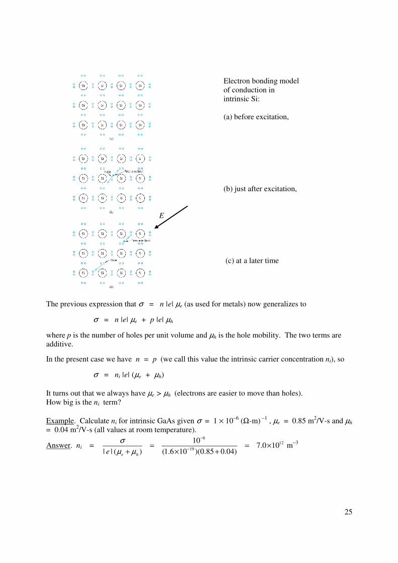
The previous expression that σ = n |e| µe (as used for metals) now generalizes to
σ = n |e| µe + p |e| µh
where p is the number of holes per unit volume and µh is the hole mobility. The two terms are
additive.
In the present case we have n = p (we call this value the intrinsic carrier concentration ni), so
σ = ni |e| (µe + µh)
It turns out that we always have µe > µh (electrons are easier to move than holes).
How big is the ni term?
Example. Calculate ni for intrinsic GaAs given σ = 1 × 10⁻⁶
(Ω-m) −1
, µe = 0.85 m2/V-s and µh
= 0.04 m2/V-s (all values at room temperature).
Answer. ni = 6
12
19
107.0 10
| | ( ) (1.6 10 )(0.85 0.04)e he
σ
µ µ
−
−= = ×
+ × + m−3
Electron bonding model
of conduction in
intrinsic Si:
(a) before excitation,
(b) just after excitation,
(c) at a later time
26
Variation of ni with temperature: At T = 0 Kelvin there would be no thermal effects to excite
electrons from the valence band to the conduction band (ni → 0). When T > 0 there is a thermal
Boltzmann factor like exp(−Eg/kBT) for the probability of electron excitation this will increase
sharply with T.
A detailed calculation shows that ni is proportional to exp(−Eg/2kBT), so roughly σ is
proportional to the same factors (since mobilities do not usually change much with T).
EXTRINSIC CONDUCTIVITY
− This is applicable when there are selected impurities in the semiconductor with
concentrations comparable to (or larger than) the calculated ni.
There are 2 cases of interest, called n-type and p-type.
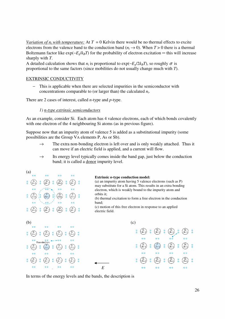
1) n-type extrinsic semiconductors
As an example, consider Si. Each atom has 4 valence electrons, each of which bonds covalently
with one electron of the 4 neighbouring Si atoms (as in previous figure).
Suppose now that an impurity atom of valence 5 is added as a substitutional impurity (some
possibilities are the Group VA elements P, As or Sb).
→ The extra non-bonding electron is left over and is only weakly attached. Thus it
can move if an electric field is applied, and a current will flow.
→ Its energy level typically comes inside the band gap, just below the conduction
band; it is called a donor impurity level.
(a)
(b) (c)
E
In terms of the energy levels and the bands, the description is
Extrinsic n-type conduction model: (a) an impurity atom having 5 valence electrons (such as P)
may substitute for a Si atom. This results in an extra bonding
electron, which is weakly bound to the impurity atom and
orbits it;
(b) thermal excitation to form a free electron in the conduction
band;
(c) motion of this free electron in response to an applied
electric field.

27
Notice that the process does not cause any holes to be formed in the valence band.
∴ n >> p in this case (and hence the name n-type)
For the conductivity, σ ≅ n |e| µe , and the electrons are called the majority carriers. Also the
temperature dependence should be different from the intrinsic case because the excitation energy
is much smaller (see later).
2) p-type extrinsic semiconductors
We again use Si as an example, but in this case we add a substitutional impurity that has valence
3 from group IIIA (e.g. Al, B, or Ga). This produces the opposite effect to the previous case:
there is now a deficiency of one electron in one of the covalent bonds
→ This is like having one hole that is only loosely attached.
→ It’s energy level again comes within the band gap, but it is now just above the
valence band. It is called an acceptor impurity level.
(a) An impurity atom having 3 valence electrons (such as B) may substitute for a Si atom. This results in a
deficiency of 1 valence electron (or equivalently the presence of a hole) associated with the impurity atom. (b) The
motion of this hole in response to an electric field.
(a) Electron energy band
scheme for a donor impurity
level located within the band
gap, just below the bottom of
the conduction band.
(b) Excitation from a donor
state to produce a free electron
in the conduction band.
Extrinsic p-type
conduction model:
(a) Electron energy band
scheme for an acceptor
impurity level located
within the band gap, just
above the top of the
valence band.
(b) Excitation of an
electron into the acceptor
level to leave a free hole
in the valence band.

28
This process leaves holes at the top of the valence band, but it does not form electrons in the
conduction band.
∴ p >> n in this case (and hence the name p-type)
We have σ ≅ p |e| µh , and the holes are called the majority carriers.
The process of intentionally adding the impurities to form n-type or p-type semiconductors as an
alloy is called doping.
Temperature dependence of σ in semiconductors
— this comes from the T-dependence of the carrier concentrations (n and/or p) and
the T-dependence of the mobilities (µe and/or µh)
— the behaviour for the intrinsic and extrinsic situations can be discussed as follows.
Intrinsic carrier concentration ni
(log scale) vs. temperature T for Si
and Ge.
Electron concentration n vs. T for
n-type Si doped with 1021
m-3
of a
donor impurity. The freeze-out,
extrinsic and intrinsic regimes are
shown.

29
To deduce the conductivity σ, we also need to know something about the T-dependence and
impurity dependence of the electron and hole mobilities.
Dependence of (a) the electron mobility and (b) the hole mobility (log scales) vs. T (log scales)
for Si with various impurity concentrations.
Dependence of the room-
temperature electron and
hole mobilities (log scale)
vs. impurity concentration
(log scale) for Si.

![PERIODIC CLASSIFICATION & PERIODIC PROPERTIES [ 1 ...youvaacademy.com/youvaadmin/image/PERIODIC TABLE BY RS.pdf · [ 2 ] PERIODIC CLASSIFICATION & PERIODIC PROPERTIES BY RAJESH SHAH](https://img.dokumen.tips/doc/110x75/604570870a43592d4f6b3e29/periodic-classification-periodic-properties-1-table-by-rspdf-2.jpg)