Embed Size (px)
Citation preview
February 2011 Doc ID 1499 Rev 3 1/30
1
TDA7360
22 W bridge/stereo audio amplifier with clipping detector
Features■ Very few external components
■ No Boucherot cells
■ No bootstrap capacitors
■ High output power
■ No switch on/off noise
■ Very low standby current
■ Fixed gain (20 dB stereo)
■ Programmable turn-on delay
■ Clipping detector
■ Protections:– Output AC-DC short circuit to ground and
to supply voltage– Very inductive loads– Loudspeaker protection– Overrating chip temperature– Load dump voltage– Fortuitous open ground– ESD
DescriptionThe TDA7360 is a new technology class AB Audio Power Amplifier in the Multiwatt® package designed for car radio applications.
Thanks to the fully complementary PNP/NPN output configuration the high power performance of the TDA7360 is obtained without bootstrap capacitors.
A delayed turn-on mute circuit eliminates audible on/off noise, and a novel short circuit protection system prevents spurious intervention with highly inductive loads.
The device provides a circuit for the detection of clipping in the output stages. The output, an open collector, is able to drive systems with automatic volume control.
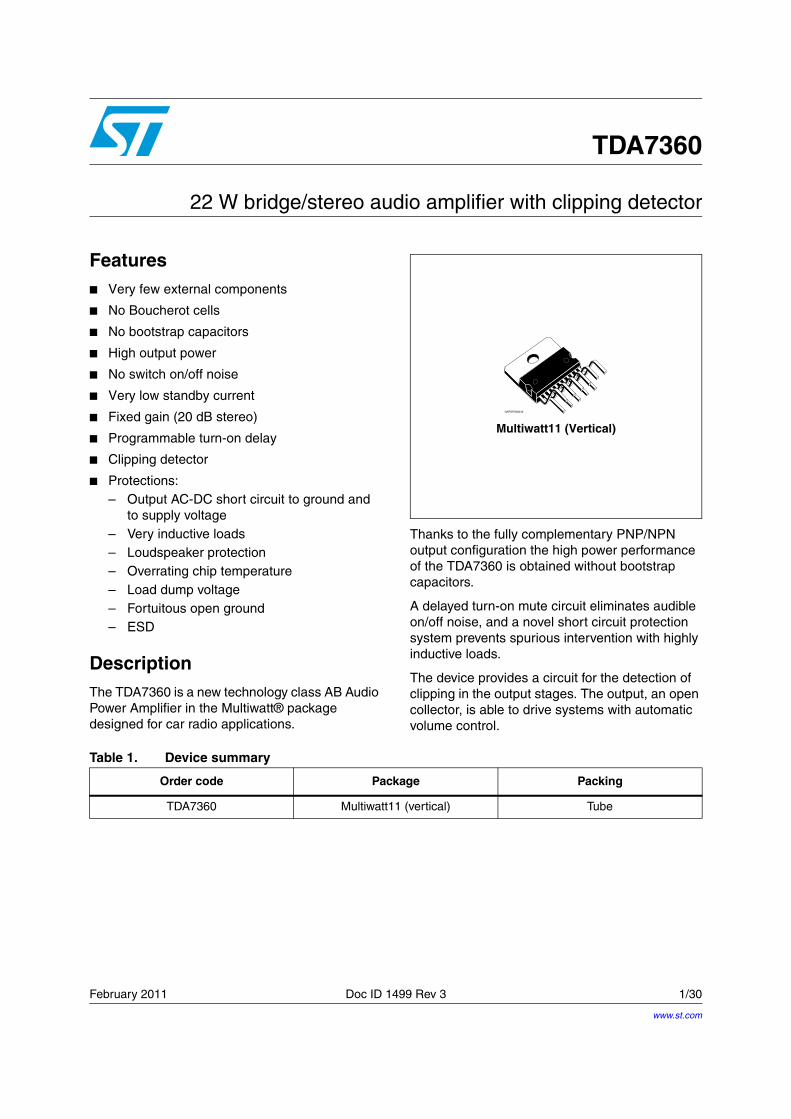
Multiwatt11 (Vertical)
Table 1. Device summary
Order code Package Packing
TDA7360 Multiwatt11 (vertical) Tube
www.st.com

Contents TDA7360
2/30 Doc ID 1499 Rev 3
Contents
1 Block and pins connection diagram . . . . . . . . . . . . . . . . . . . . . . . . . . . . 6
2 Electrical specifications . . . . . . . . . . . . . . . . . . . . . . . . . . . . . . . . . . . . . . 8
2.1 Absolute maximum ratings . . . . . . . . . . . . . . . . . . . . . . . . . . . . . . . . . . . . . 8
2.2 Thermal data . . . . . . . . . . . . . . . . . . . . . . . . . . . . . . . . . . . . . . . . . . . . . . . 8
2.3 Electrical characteristics . . . . . . . . . . . . . . . . . . . . . . . . . . . . . . . . . . . . . . . 8
2.4 Test and application circuit . . . . . . . . . . . . . . . . . . . . . . . . . . . . . . . . . . . . 10
2.5 Electrical characteristics curves . . . . . . . . . . . . . . . . . . . . . . . . . . . . . . . . 12
3 General description . . . . . . . . . . . . . . . . . . . . . . . . . . . . . . . . . . . . . . . . . 15
3.1 Amplifier organization . . . . . . . . . . . . . . . . . . . . . . . . . . . . . . . . . . . . . . . . 15
3.2 Block description . . . . . . . . . . . . . . . . . . . . . . . . . . . . . . . . . . . . . . . . . . . 15
3.2.1 Polarization . . . . . . . . . . . . . . . . . . . . . . . . . . . . . . . . . . . . . . . . . . . . . . 15
3.2.2 SVR . . . . . . . . . . . . . . . . . . . . . . . . . . . . . . . . . . . . . . . . . . . . . . . . . . . . 15
3.2.3 Delayed turn-on (muting) . . . . . . . . . . . . . . . . . . . . . . . . . . . . . . . . . . . . 15
3.2.4 Stereo/bridge switching . . . . . . . . . . . . . . . . . . . . . . . . . . . . . . . . . . . . . 16
3.2.5 Standby . . . . . . . . . . . . . . . . . . . . . . . . . . . . . . . . . . . . . . . . . . . . . . . . . 16
3.2.6 Stability . . . . . . . . . . . . . . . . . . . . . . . . . . . . . . . . . . . . . . . . . . . . . . . . . 16
3.2.7 Clip detector . . . . . . . . . . . . . . . . . . . . . . . . . . . . . . . . . . . . . . . . . . . . . . 17
3.2.8 Output stage . . . . . . . . . . . . . . . . . . . . . . . . . . . . . . . . . . . . . . . . . . . . . 18
3.2.9 Amplifier block diagram . . . . . . . . . . . . . . . . . . . . . . . . . . . . . . . . . . . . . 19
3.3 Built-in protection systems . . . . . . . . . . . . . . . . . . . . . . . . . . . . . . . . . . . . 20
3.3.1 Short circuit protection . . . . . . . . . . . . . . . . . . . . . . . . . . . . . . . . . . . . . . 20
3.3.2 Load dump voltage surge . . . . . . . . . . . . . . . . . . . . . . . . . . . . . . . . . . . 20
3.3.3 Polarity inversion . . . . . . . . . . . . . . . . . . . . . . . . . . . . . . . . . . . . . . . . . . 21
3.4 Open ground . . . . . . . . . . . . . . . . . . . . . . . . . . . . . . . . . . . . . . . . . . . . . . 21
3.4.1 DC voltage . . . . . . . . . . . . . . . . . . . . . . . . . . . . . . . . . . . . . . . . . . . . . . . 21
3.4.2 Thermal shut-down . . . . . . . . . . . . . . . . . . . . . . . . . . . . . . . . . . . . . . . . 22
3.4.3 Loudspeaker protection . . . . . . . . . . . . . . . . . . . . . . . . . . . . . . . . . . . . . 22
4 Application hints . . . . . . . . . . . . . . . . . . . . . . . . . . . . . . . . . . . . . . . . . . . 23
4.1 Reducing turn on-off pop . . . . . . . . . . . . . . . . . . . . . . . . . . . . . . . . . . . . . 23
4.2 Turn-on . . . . . . . . . . . . . . . . . . . . . . . . . . . . . . . . . . . . . . . . . . . . . . . . . . . 23

TDA7360 Contents
Doc ID 1499 Rev 3 3/30
4.3 Turn-off . . . . . . . . . . . . . . . . . . . . . . . . . . . . . . . . . . . . . . . . . . . . . . . . . . . 24
4.4 Global approach to solving pop problem by using the muting/turn-on delay function 25
4.5 Balance input in bridge configuration . . . . . . . . . . . . . . . . . . . . . . . . . . . . 27
5 Package information . . . . . . . . . . . . . . . . . . . . . . . . . . . . . . . . . . . . . . . . 28
6 Revision history . . . . . . . . . . . . . . . . . . . . . . . . . . . . . . . . . . . . . . . . . . . 29
List of tables TDA7360
4/30 Doc ID 1499 Rev 3
List of tables
Table 1. Device summary . . . . . . . . . . . . . . . . . . . . . . . . . . . . . . . . . . . . . . . . . . . . . . . . . . . . . . . . . . 1Table 2. Absolute maximum ratings . . . . . . . . . . . . . . . . . . . . . . . . . . . . . . . . . . . . . . . . . . . . . . . . . . 8Table 3. Thermal data. . . . . . . . . . . . . . . . . . . . . . . . . . . . . . . . . . . . . . . . . . . . . . . . . . . . . . . . . . . . . 8Table 4. Electrical characteristics . . . . . . . . . . . . . . . . . . . . . . . . . . . . . . . . . . . . . . . . . . . . . . . . . . . . 8Table 5. External components value of the stereo test and application circuits . . . . . . . . . . . . . . . . 10Table 6. Document revision history . . . . . . . . . . . . . . . . . . . . . . . . . . . . . . . . . . . . . . . . . . . . . . . . . 29

TDA7360 List of figures
Doc ID 1499 Rev 3 5/30
List of figures
Figure 1. Block diagram (stereo configuration) . . . . . . . . . . . . . . . . . . . . . . . . . . . . . . . . . . . . . . . . . . 6Figure 2. Block diagram (bridge configuration) . . . . . . . . . . . . . . . . . . . . . . . . . . . . . . . . . . . . . . . . . . 6Figure 3. Pins connection (top view) . . . . . . . . . . . . . . . . . . . . . . . . . . . . . . . . . . . . . . . . . . . . . . . . . . 7Figure 4. Stereo test and application circuit . . . . . . . . . . . . . . . . . . . . . . . . . . . . . . . . . . . . . . . . . . . . 10Figure 5. Printed circuit board of the stereo application circuit . . . . . . . . . . . . . . . . . . . . . . . . . . . . . 10Figure 6. Bridge test and application circuit . . . . . . . . . . . . . . . . . . . . . . . . . . . . . . . . . . . . . . . . . . . . 11Figure 7. Printed circuit board of the bridge application circuit . . . . . . . . . . . . . . . . . . . . . . . . . . . . . 11Figure 8. Output power vs. supply voltage (Stereo, 4 Ω) . . . . . . . . . . . . . . . . . . . . . . . . . . . . . . . . . . 12Figure 9. Output power vs. supply voltage (Stereo, 2 Ω) . . . . . . . . . . . . . . . . . . . . . . . . . . . . . . . . . . 12Figure 10. Output power vs. supply voltage (Stereo, 3.2 Ω) . . . . . . . . . . . . . . . . . . . . . . . . . . . . . . . . 12Figure 11. Output power vs. supply voltage (Bridge, 4 Ω) . . . . . . . . . . . . . . . . . . . . . . . . . . . . . . . . . . 12Figure 12. Output power vs. supply voltage (Bridge, 3.2 Ω) . . . . . . . . . . . . . . . . . . . . . . . . . . . . . . . . 12Figure 13. Drain current vs. supply voltage (Stereo) . . . . . . . . . . . . . . . . . . . . . . . . . . . . . . . . . . . . . . 12Figure 14. Distortion vs. output power (Stereo, 4 Ω) . . . . . . . . . . . . . . . . . . . . . . . . . . . . . . . . . . . . . . 13Figure 15. Distortion vs. output power (Stereo, 3.2 Ω). . . . . . . . . . . . . . . . . . . . . . . . . . . . . . . . . . . . . 13Figure 16. Distortion vs. output power (Stereo, 2 Ω) . . . . . . . . . . . . . . . . . . . . . . . . . . . . . . . . . . . . . . 13Figure 17. Distortion vs. output power (Bridge, 4 Ω) . . . . . . . . . . . . . . . . . . . . . . . . . . . . . . . . . . . . . . 13Figure 18. Distortion vs. output power (Bridge, 3.2 Ω). . . . . . . . . . . . . . . . . . . . . . . . . . . . . . . . . . . . . 13Figure 19. SVR vs. frequency and C3 (Stereo) . . . . . . . . . . . . . . . . . . . . . . . . . . . . . . . . . . . . . . . . . . 13Figure 20. SVR vs. frequency and C3 (Bridge) . . . . . . . . . . . . . . . . . . . . . . . . . . . . . . . . . . . . . . . . . . 14Figure 21. Crosstalk vs. frequency (Stereo) . . . . . . . . . . . . . . . . . . . . . . . . . . . . . . . . . . . . . . . . . . . . 14Figure 22. Power dissipation and efficiency vs. output power (Stereo, 2 Ω) . . . . . . . . . . . . . . . . . . . . 14Figure 23. Power dissipation and efficiency vs. output power (Stereo, 4 Ω) . . . . . . . . . . . . . . . . . . . . 14Figure 24. Power dissipation and efficiency vs. output power (Bridge, 4 Ω) . . . . . . . . . . . . . . . . . . . . 14Figure 25. Power dissipation and efficiency vs. output power (Bridge, 3.2 Ω). . . . . . . . . . . . . . . . . . . 14Figure 26. Turn-on delay circuit . . . . . . . . . . . . . . . . . . . . . . . . . . . . . . . . . . . . . . . . . . . . . . . . . . . . . . 16Figure 27. Mute function diagram . . . . . . . . . . . . . . . . . . . . . . . . . . . . . . . . . . . . . . . . . . . . . . . . . . . . 17Figure 28. Dual channel distortion detector . . . . . . . . . . . . . . . . . . . . . . . . . . . . . . . . . . . . . . . . . . . . . 17Figure 29. Output at clipping detector pin vs. signal distortion . . . . . . . . . . . . . . . . . . . . . . . . . . . . . . 17Figure 30. ICV - PNP gain vs. IC . . . . . . . . . . . . . . . . . . . . . . . . . . . . . . . . . . . . . . . . . . . . . . . . . . . . . 18Figure 31. ICV - PNP VCE(sat) vs. IC . . . . . . . . . . . . . . . . . . . . . . . . . . . . . . . . . . . . . . . . . . . . . . . . . 18Figure 32. ICV - PNP cut-off frequency vs. IC . . . . . . . . . . . . . . . . . . . . . . . . . . . . . . . . . . . . . . . . . . . 18Figure 33. The new output stage . . . . . . . . . . . . . . . . . . . . . . . . . . . . . . . . . . . . . . . . . . . . . . . . . . . . . 19Figure 34. A classical output stage . . . . . . . . . . . . . . . . . . . . . . . . . . . . . . . . . . . . . . . . . . . . . . . . . . . 19Figure 35. Amplifier block diagram . . . . . . . . . . . . . . . . . . . . . . . . . . . . . . . . . . . . . . . . . . . . . . . . . . . 19Figure 36. Circuitry for short circuit detection . . . . . . . . . . . . . . . . . . . . . . . . . . . . . . . . . . . . . . . . . . . 20Figure 37. Suggested LC network circuit . . . . . . . . . . . . . . . . . . . . . . . . . . . . . . . . . . . . . . . . . . . . . . . 21Figure 38. Voltage gain bridge configuration . . . . . . . . . . . . . . . . . . . . . . . . . . . . . . . . . . . . . . . . . . . . 21Figure 39. Maximum allowable power dissipation vs. ambient temperature . . . . . . . . . . . . . . . . . . . . 22Figure 40. Restart circuit . . . . . . . . . . . . . . . . . . . . . . . . . . . . . . . . . . . . . . . . . . . . . . . . . . . . . . . . . . . 22Figure 41. Output waveforms compared to the values of Csvr . . . . . . . . . . . . . . . . . . . . . . . . . . . . . . 24Figure 42. ST-BY pin supply circuit, example 1 . . . . . . . . . . . . . . . . . . . . . . . . . . . . . . . . . . . . . . . . . . 25Figure 43. ST-BY pin supply circuit, example 2 . . . . . . . . . . . . . . . . . . . . . . . . . . . . . . . . . . . . . . . . . . 25Figure 44. Suggested muting circuit during amplifier switch-on and switch-off . . . . . . . . . . . . . . . . . . 26Figure 45. Timing diagram for the circuit depicted in fig. 44 . . . . . . . . . . . . . . . . . . . . . . . . . . . . . . . . 26Figure 46. Modification of the circuit depicted in fig.44 to drive two amplifiers . . . . . . . . . . . . . . . . . . 26Figure 47. Balance input bridge configuration, example 1 . . . . . . . . . . . . . . . . . . . . . . . . . . . . . . . . . . 27Figure 48. Balance input bridge configuration, example 2 . . . . . . . . . . . . . . . . . . . . . . . . . . . . . . . . . . 27Figure 49. Multiwatt11 (vertical) mechanical data and package dimensions. . . . . . . . . . . . . . . . . . . . 28

Block and pins connection diagram TDA7360
6/30 Doc ID 1499 Rev 3
1 Block and pins connection diagram
Figure 1. Block diagram (stereo configuration)
Figure 2. Block diagram (bridge configuration)

TDA7360 Block and pins connection diagram
Doc ID 1499 Rev 3 7/30
Figure 3. Pins connection (top view)

Electrical specifications TDA7360
8/30 Doc ID 1499 Rev 3
2 Electrical specifications
2.1 Absolute maximum ratings
2.2 Thermal data
2.3 Electrical characteristicsRefer to the test circuits, Tamb = 25 °C, VS = 14.4 V, f = 1 kHz unless otherwise specified.
Table 2. Absolute maximum ratings
Symbol Parameter Value Unit
VS Operating supply voltage 18 V
VS DC supply voltage 28 V
VS Peak supply voltage (t = 50 ms) 50 V
IO Output peak current (non rep. t = 100 µs) 5 A
IO Output peak current (rep. freq. > 10 Hz) 4 A
Ptot Power dissipation at Tcase = 85 °C 36 W
Tstg, Tj Storage and junction temperature -40 to 150 °C
Table 3. Thermal data
Symbol Parameter Value Unit
Rthj-case Thermal resistance junction-to-case Max. 1.8 °C/W
Table 4. Electrical characteristics
Symbol Parameter Test condition Min. Typ. Max. Unit
VS Supply voltage range - 8 - 18 V
Id Total quiescent drain current Stereo configuration - - 120 mA
ASB Standby attenuation - 60 80 - dB
ISB Standby current - - - 100 µA
ICO Clip detector average current
Pin 2 pull up to 5 V with 10 kΩd = 1%
d = 5%
- 70
130
- µA
Stereo
Po Output power (each channel)
d = 10%
RL= 1.6 ΩRL= 2 ΩRL= 3.2 ΩRL= 4 Ω
7
1211
8
6.5
- W

TDA7360 Electrical specifications
Doc ID 1499 Rev 3 9/30
d Distortion Po = 0.1 to 4 W; RL = 3.2 Ω - 0.05 0.5 %
SVR Supply voltage rejection Rg = 10 kΩ, f = 100 HzC3 = 22 µF
C3 = 100 µF45
62
- dB
CT Crosstalk f = 1 kHz
f = 10 kHz 45
55- dB
RI Input resistance - - 50 - kΩ
GV Voltage gain - - 20 - dB
GV Voltage gain match - - 1 dB
EIN Input noise voltage
22 Hz to 22 kHz
Rg = 50 ΩRg = 10 kΩRg = ∞
-2.5
3
3.5
7 µV
Bridge
VOS Output offset voltage - - - 250 mV
Po Output power d = 10%; RL= 4 Ω
d = 10%; RL= 3.2 Ω 16
20
22 - W
d Distortion Po = 0.1 to 10 W; RL = 3.2 Ω 0.05 1 %
SVR Supply voltage rejection Rg = 10kΩ f = 100HzC3 = 22µF
C3 = 100µF
45
62
- dB
RI Input resistance - - 50 - kΩ
GV Voltage gain - - 26 - dB
EIN Input noise voltage 22 Hz to 22 kHz Rg= 50 Ω
Rg= 10 kΩ-
3.5
4 - µV
Table 4. Electrical characteristics (continued)
Symbol Parameter Test condition Min. Typ. Max. Unit
Electrical specifications TDA7360
10/30 Doc ID 1499 Rev 3
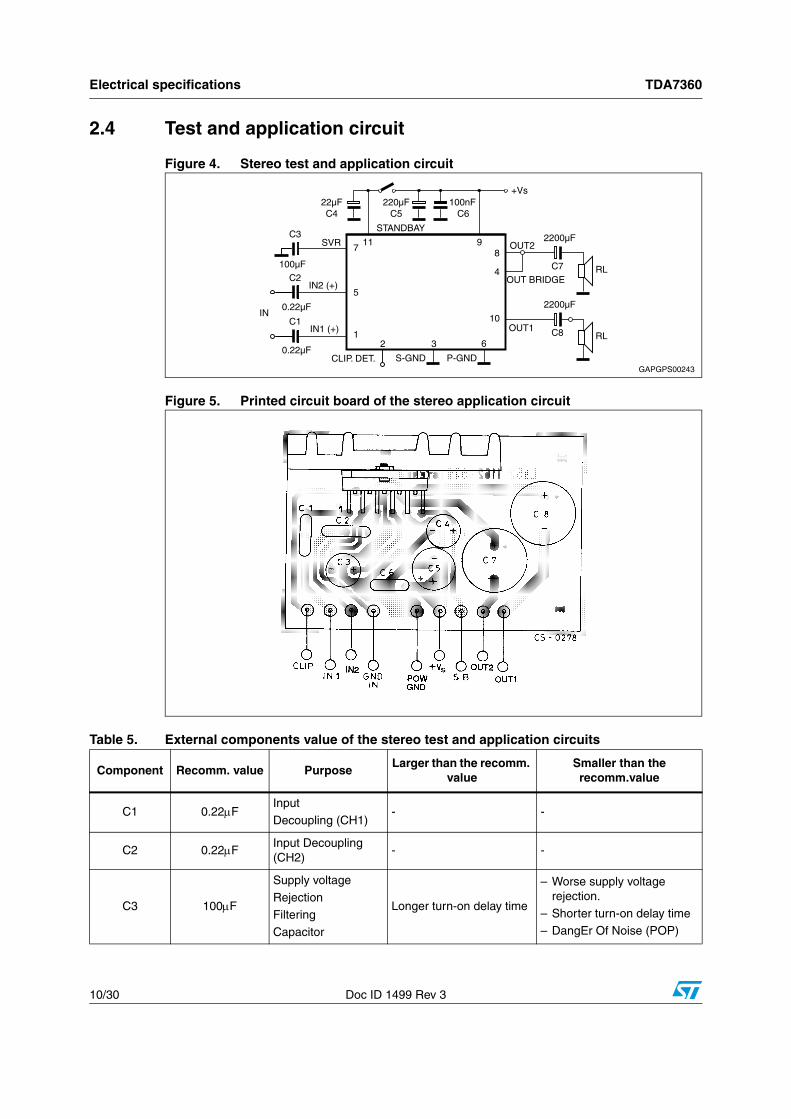
2.4 Test and application circuit
Figure 4. Stereo test and application circuit
Figure 5. Printed circuit board of the stereo application circuit
Table 5. External components value of the stereo test and application circuits
Component Recomm. value PurposeLarger than the recomm.
valueSmaller than the recomm.value
C1 0.22μFInput
Decoupling (CH1)- -
C2 0.22μF Input Decoupling (CH2)
- -
C3 100μF
Supply voltage
RejectionFiltering
Capacitor
Longer turn-on delay time
– Worse supply voltage rejection.
– Shorter turn-on delay time– DangEr Of Noise (POP)

TDA7360 Electrical specifications
Doc ID 1499 Rev 3 11/30
Figure 6. Bridge test and application circuit
Figure 7. Printed circuit board of the bridge application circuit
C4 22μF StandbyON/OFF delay
Delayed turn-off by standby switch
Danger of noise (POP)
C5 220μF (min) Supply by-pass - Danger of oscillations
C6 100nF (min) Supply by-pass - Danger of oscillations
C7 2200μF
Output
Decoupling
CH2
– Decrease of low frequency cut-off
– Longer turn-on delay
– Increase of low frequency cut-off
– Shorter turn-on delay
Table 5. External components value of the stereo test and application circuits (continued)
Component Recomm. value PurposeLarger than the recomm.
valueSmaller than the recomm.value

Electrical specifications TDA7360
12/30 Doc ID 1499 Rev 3
2.5 Electrical characteristics curves
Figure 8. Output power vs. supply voltage (Stereo, 4 Ω)
Figure 9. Output power vs. supply voltage (Stereo, 2 Ω)
Figure 10. Output power vs. supply voltage (Stereo, 3.2 Ω)
Figure 11. Output power vs. supply voltage (Bridge, 4 Ω)
Figure 12. Output power vs. supply voltage (Bridge, 3.2 Ω)
Figure 13. Drain current vs. supply voltage (Stereo)

TDA7360 Electrical specifications
Doc ID 1499 Rev 3 13/30
Figure 14. Distortion vs. output power (Stereo, 4 Ω)
Figure 15. Distortion vs. output power (Stereo, 3.2 Ω)
Figure 16. Distortion vs. output power (Stereo, 2 Ω)
Figure 17. Distortion vs. output power (Bridge, 4 Ω)
Figure 18. Distortion vs. output power (Bridge, 3.2 Ω)
Figure 19. SVR vs. frequency and C3 (Stereo)

Electrical specifications TDA7360
14/30 Doc ID 1499 Rev 3
Figure 20. SVR vs. frequency and C3 (Bridge) Figure 21. Crosstalk vs. frequency (Stereo)
Figure 22. Power dissipation and efficiency vs. output power (Stereo, 2 Ω)
Figure 23. Power dissipation and efficiency vs. output power (Stereo, 4 Ω)
Figure 24. Power dissipation and efficiency vs. output power (Bridge, 4 Ω)
Figure 25. Power dissipation and efficiency vs. output power (Bridge, 3.2 Ω)

TDA7360 General description
Doc ID 1499 Rev 3 15/30
3 General description
3.1 Amplifier organizationThe TDA7360 has been developed taking care of the key concepts of the modern power audio amplifier for car radio such as: space and costs saving due to the minimized external count, excellent electrical performances, flexibility in use, superior reliability thanks to a built-in array of protections. As a result the following performances has been achieved:
– No need of bootstrap capacitors even at the highest output power levels
– Absolute stability without external compensation thanks to the innovative out stage configuration, also allowing internally fixed closed loop lower than competitors
– Low gain (20 dB stereo fixed without any external components) in order to minimize the output noise and optimize SVR
– Silent Mute/Standby function featuring absence of pop ON/OFF noise
– high SVR
– Stereo/bridge operation without addition of external component
– AC/DC short circuit protection (to GND, to VS, across the load)
– Loudspeaker protection
– Dump protection
– ESD protection
3.2 Block description
3.2.1 Polarization
The device is organized with the gain resistors directly connected to the signal ground pin i.e. without gain capacitors (Figure 1).
The non inverting inputs of the amplifiers are connected to the SVR pin by means of resistor dividers, equal to the feedback networks. This allows the outputs to track the SVR pin which is sufficiently slow to avoid audible turn-on and turn-off transients.
3.2.2 SVR
The voltage ripple on the outputs is equal to the one on SVR pin: with appropriate selection of CSVR, more than 60dB of ripple rejection can be obtained.
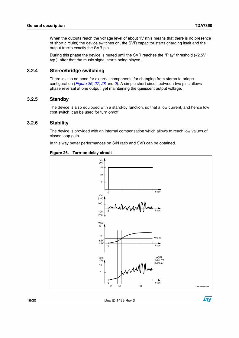
3.2.3 Delayed turn-on (muting)
The CSVR sets a signal turn-on delay too. A circuit is included which mutes the device until the voltage on SVR pin reaches ~2.5V typ (Figure 1). The mute function is obtained by duplicating the input differential pair (Figure 27): it can be switched to the signal source or to an internal mute input. This feature is necessary to prevent transients at the inputs reaching the loudspeaker(s) immediately after power-on).
Figure 1 represents the detailed turn-on transient with reference to the stereo configuration. At the power-on the output decoupling capacitors are charged through an internal path but the device itself remains switched off (Phase 1 of the represented diagram).
General description TDA7360
16/30 Doc ID 1499 Rev 3
When the outputs reach the voltage level of about 1V (this means that there is no presence of short circuits) the device switches on, the SVR capacitor starts charging itself and the output tracks exactly the SVR pin.
During this phase the device is muted until the SVR reaches the "Play" threshold (~2.5V typ.), after that the music signal starts being played.
3.2.4 Stereo/bridge switching
There is also no need for external components for changing from stereo to bridge configuration (Figure 26, 27, 28 and 2). A simple short circuit between two pins allows phase reversal at one output, yet maintaining the quiescent output voltage.
3.2.5 Standby
The device is also equipped with a stand-by function, so that a low current, and hence low cost switch, can be used for turn on/off.
3.2.6 Stability
The device is provided with an internal compensation which allows to reach low values of closed loop gain.
In this way better performances on S/N ratio and SVR can be obtained.
Figure 26. Turn-on delay circuit

TDA7360 General description
Doc ID 1499 Rev 3 17/30
Figure 27. Mute function diagram
3.2.7 Clip detector
The TDA7360 is equipped with an internal circuit able to detect the output stage saturation providing a proper current sinking into an open collector out. pin 2) when a certain distortion level is reached at each output. This particular function allows compression facility whenever the amplifier is over driven, so obtaining high quality sound at all listening levels.
Figure 28. Dual channel distortion detector
Figure 29. Output at clipping detector pin vs. signal distortion
General description TDA7360
18/30 Doc ID 1499 Rev 3
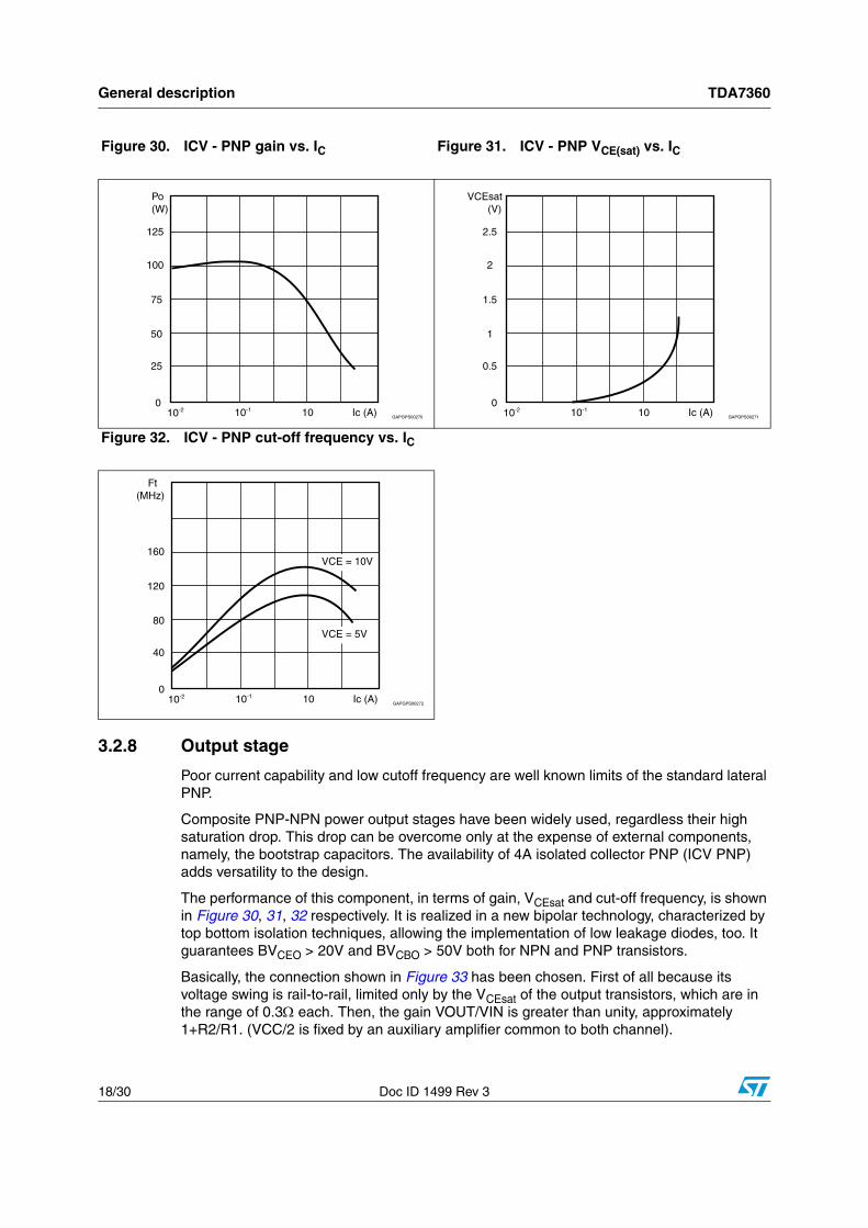
3.2.8 Output stage
Poor current capability and low cutoff frequency are well known limits of the standard lateral PNP.
Composite PNP-NPN power output stages have been widely used, regardless their high saturation drop. This drop can be overcome only at the expense of external components, namely, the bootstrap capacitors. The availability of 4A isolated collector PNP (ICV PNP) adds versatility to the design.
The performance of this component, in terms of gain, VCEsat and cut-off frequency, is shown in Figure 30, 31, 32 respectively. It is realized in a new bipolar technology, characterized by top bottom isolation techniques, allowing the implementation of low leakage diodes, too. It guarantees BVCEO > 20V and BVCBO > 50V both for NPN and PNP transistors.
Basically, the connection shown in Figure 33 has been chosen. First of all because its voltage swing is rail-to-rail, limited only by the VCEsat of the output transistors, which are in the range of 0.3Ω each. Then, the gain VOUT/VIN is greater than unity, approximately 1+R2/R1. (VCC/2 is fixed by an auxiliary amplifier common to both channel).
Figure 30. ICV - PNP gain vs. IC Figure 31. ICV - PNP VCE(sat) vs. IC
Figure 32. ICV - PNP cut-off frequency vs. IC

TDA7360 General description
Doc ID 1499 Rev 3 19/30
It is possible, controlling the amount of this local feedback, to force the loop gain (A. β) to less than unity at frequencies for which the phase shift is 180°. This means that the output buffer is intrinsically stable and not prone to oscillation.
Figure 33. The new output stage
In contrast, with the circuit of Figure 34, the solution adopted to reduce the gain at high frequencies is the use of an external RC network.
Figure 34. A classical output stage
3.2.9 Amplifier block diagram
The block diagram of each voltage amplifier is shown in Figure 35. Regardless of production spread, the current in each final stage is kept low, with enough margin on the minimum, below which cross-over distortion would appear.
Figure 35. Amplifier block diagram
General description TDA7360
20/30 Doc ID 1499 Rev 3
3.3 Built-in protection systems
3.3.1 Short circuit protection
The maximum current the device can deliver can be calculated by considering the voltage that may be present at the terminals of a car radio amplifier and the minimum load impedance.
Apart from consideration concerning the area of the power transistors it is not difficult to achieve peak currents of this magnitude (5A peak).
However, it becomes more complicated if AC and DC short circuit protection is also required.In particular, with a protection circuit which limits the output current following the SOA curve of the output transistors it is possible that in some conditions (highly reactive loads, for example) the protection circuit may intervene during normal operation. For this reason each amplifier has been equipped with a protection circuit that intervenes when the output current exceeds 4A.
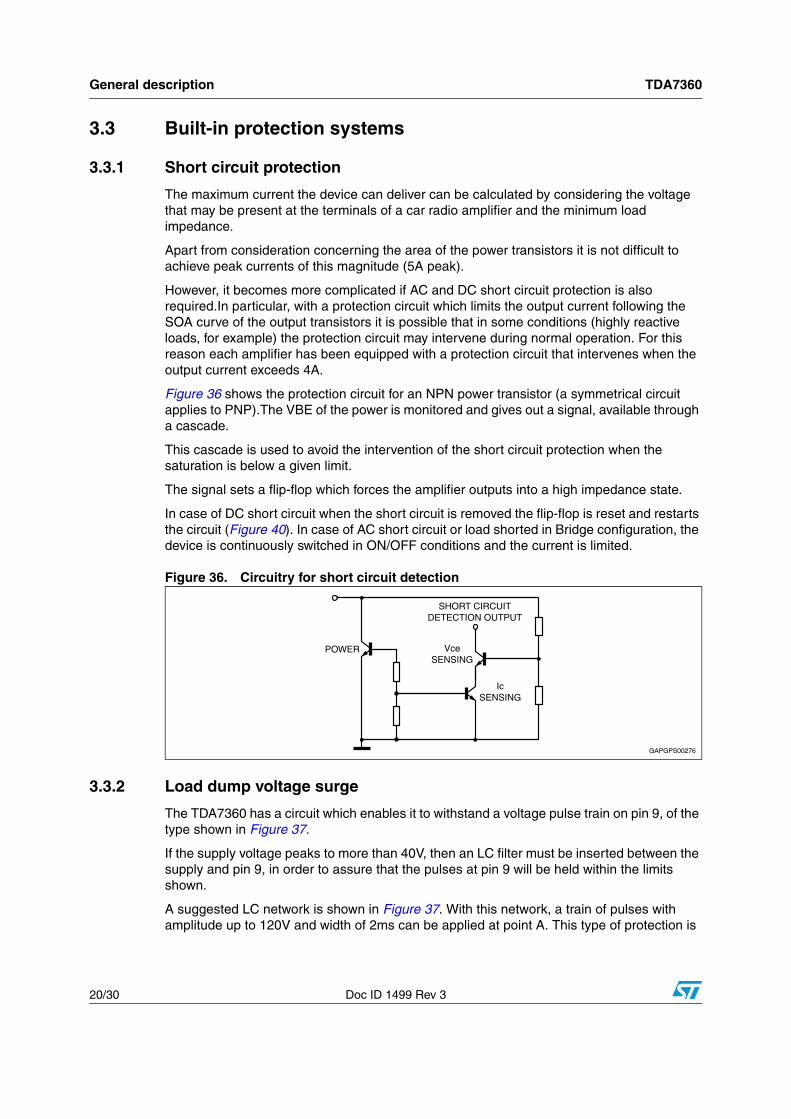
Figure 36 shows the protection circuit for an NPN power transistor (a symmetrical circuit applies to PNP).The VBE of the power is monitored and gives out a signal, available through a cascade.
This cascade is used to avoid the intervention of the short circuit protection when the saturation is below a given limit.
The signal sets a flip-flop which forces the amplifier outputs into a high impedance state.
In case of DC short circuit when the short circuit is removed the flip-flop is reset and restarts the circuit (Figure 40). In case of AC short circuit or load shorted in Bridge configuration, the device is continuously switched in ON/OFF conditions and the current is limited.
Figure 36. Circuitry for short circuit detection
3.3.2 Load dump voltage surge
The TDA7360 has a circuit which enables it to withstand a voltage pulse train on pin 9, of the type shown in Figure 37.
If the supply voltage peaks to more than 40V, then an LC filter must be inserted between the supply and pin 9, in order to assure that the pulses at pin 9 will be held within the limits shown.
A suggested LC network is shown in Figure 37. With this network, a train of pulses with amplitude up to 120V and width of 2ms can be applied at point A. This type of protection is

TDA7360 General description
Doc ID 1499 Rev 3 21/30
ON when the supply voltage (pulse or DC) exceeds 18V. For this reason the maximum operating supply voltage is 18V.
Figure 37. Suggested LC network circuit
Figure 38. Voltage gain bridge configuration
3.3.3 Polarity inversion
High current (up to 10A) can be handled by the device with no damage for a longer period than the blow-out time of a quick 2A fuse (normally connected in series with the supply). This features is added to avoid destruction, if during fitting to the car, a mistake on the connection of the supply is made.
3.4 Open groundWhen the radio is in the ON condition and the ground is accidentally opened, a standard audio amplifier will be damaged. On the TDA7360 protection diodes are included to avoid any damage.
3.4.1 DC voltage
The maximum operating DC voltage for the TDA7360 is 18V. However the device can withstand a DC voltage up to 28V with no damage.
This could occur during winter if two batteries are series connected to crank the engine.

General description TDA7360
22/30 Doc ID 1499 Rev 3
3.4.2 Thermal shut-down
The presence of a thermal limiting circuit offers the following advantages:
an overload on the output (even if it is permanent), or an excessive ambient temperature can be easily withstood.
the heatsink can have a smaller factor of safety compared with that of a conventional circuit. There is no device damage in the case of excessive junction temperature: all happens is that Po (and therefore Ptot) and Id are reduced.
The maximum allowable power dissipation depends upon the size of the external heatsink (i.e. its thermal resistance); Figure 39 shows the dissipable power as a function of ambient temperature for different thermal resistance.
Figure 39. Maximum allowable power dissipation vs. ambient temperature
3.4.3 Loudspeaker protection
The TDA7360 guarantees safe operations even for the loudspeaker in case of accidental short-circuit.
Whenever a single OUT to GND, OUT to VS short circuit occurs both the outputs are switched OFF so limiting dangerous DC current flowing through the loudspeaker.
Figure 40. Restart circuit

TDA7360 Application hints
Doc ID 1499 Rev 3 23/30
4 Application hints
This section explains briefly how to get the best from the TDA7360 and presents some application circuits with suggestions for the value of the components.These values can change depending on the characteristics that the designer of the car radio wants to obtain, or other parts of the car radio that are connected to the audio block.
To optimize the performance of the audio part it is useful (or indispensable) to analyze also the parts outside this block that can have an interconnection with the amplifier.
This method can provide components and system cost saving.
4.1 Reducing turn on-off popThe TDA7360 has been designed in a way that the turn-on (off) transients are controlled through the charge (discharge) of the Csvr capacitor.
As a result of it, the turn-on (off) transient spectrum contents is limited only to the subsonic range.The following section gives some brief notes to get the best from this design feature (it will refer mainly to the stereo application which appears to be in most cases the more critical from the pop viewpoint.The bridge connection in fact, due to the common mode waveform at the outputs, does not give pop effect).
4.2 Turn-onFigure 41 shows the output waveform (before and after the "A" weighting filter) compared to the value of Csvr.
Better pop-on performance is obtained with higher Csvr values (the recommended range is from 22μF to 220μF).
The turn-on delay (during which the amplifier is in mute condition) is a function essentially of: Cout, Csvr. Being:
T1 ≈ 120 · Cout
T2 ≈ 1200 · Csvr
The turn-on delay is given by:
T1+T2 STEREO
T2 BRIDGE
The best performance is obtained by driving the st-by pin with a ramp having a slope slower than 2V/ms.

Application hints TDA7360
24/30 Doc ID 1499 Rev 3
Figure 41. Output waveforms compared to the values of Csvr
4.3 Turn-offA turn-off pop can occur if the standby pin goes low with a short time constant (this can occur if other car radio sections, preamplifiers, radio are supplied through the same standby switch).
This pop is due to the fast switch-off of the internal current generator of the amplifier.
If the voltage present across the load becomes rapidly zero (due to the fast switch off) a small pop occurs, depending also on Cout, Rload.
The parameters that set the switch off time constant of the st-by pin are:
● the standby capacitor (Cst-by)
● the SVR capacitor (CSVR)
● resistors connected from st-by pin to ground (Rext)
The time constant is given by:
T ≈ Csvr · 2000Ω // Rext + Cst-by · 2500Ω // Rext
The suggested time constants are:
T > 120 ms with Cout =1000μF, RL = 4 ohm, stereo
T > 170 ms with Cout = 2200μF, RL = 4 ohm, stereo
If Rext is too low the Csvr can become too high and a different approach may be useful (see next section).
Figure 42 and 43 show some types of electronic switches (μP compatible) suitable for supplying the st-by pin (it is important that Qsw is able to saturate with VCE ≤ 150 mV).
Also for turn off pop the bridge configuration is superior, in particular the st-by pin can go low faster.

TDA7360 Application hints
Doc ID 1499 Rev 3 25/30
4.4 Global approach to solving pop problem by using the muting/turn-on delay functionIn the real case turn-on and turn-off pop problems are generated not only by the power amplifier, but also (very often) by preamplifiers, tone controls, radios etc. and transmitted by the power amplifier to the loudspeaker.
A simple approach to solving these problems is to use the mute characteristics of the TDA7360. If the SVR pin is at a voltage below 1.5 V, the mute attenuation (typ) is 30dB.The amplifier is in play mode when Vsvr overcomes 3.5 V.
With the circuit of Figure 44 we can mute the amplifier for a time Ton after switch-on and for a time Toff after switch-off. During this period the circuitry that precedes the power amplifier can produce spurious spikes that are not transmitted to the loudspeaker.
This can give back a very simple design of this circuitry from the pop point of view. A timing diagram of this circuit is illustrated in Figure 45. Other advantages of this circuit are:
● A reduced time constant allowance of stand-by pin turn off. Consequently it is possible to drive all the car-radio with the signal that drives this pin.
● A better turn-off noise with signal on the output. To drive two stereo amplifiers with this circuit it is possible to use the circuit of Figure 46.
Figure 42. ST-BY pin supply circuit, example 1
Figure 43. ST-BY pin supply circuit, example 2

Application hints TDA7360
26/30 Doc ID 1499 Rev 3
Figure 44. Suggested muting circuit during amplifier switch-on and switch-off
Figure 45. Timing diagram for the circuit depicted in fig. 44
Figure 46. Modification of the circuit depicted in fig.44 to drive two amplifiers

TDA7360 Application hints
Doc ID 1499 Rev 3 27/30
4.5 Balance input in bridge configurationA helpful characteristic of the TDA7360 is that, in bridge configuration, a signal present on both the input capacitors is amplified by the same amount and it is present in phase at the outputs, so this signal does not produce effects on the load.The typical value of CMRR is 46dB.
Looking at Figure 47, we can see that a noise signal from the ground of the power amplifier to the ground of the hypothetical preamplifier is amplified of a factor equal to the gain of the amplifier (2 · Gv). Using a configuration of Figure 48 the same ground noise is present at the output multiplied by the factor 2 · Gv/200.
This means less distortion, less noise (e.g. motor cassette noise) and/or a simplification of the layout of PC board.
The only limitation of this balanced input is the maximum amplitude of common mode signals (few tens of millivolt) to avoid a loss of output power due to the common mode signal on the output, but in a large number of cases this signal is within this range.
Figure 47. Balance input bridge configuration, example 1
Figure 48. Balance input bridge configuration, example 2

Package information TDA7360
28/30 Doc ID 1499 Rev 3
5 Package information
In order to meet environmental requirements, ST offers these devices in different grades of ECOPACK® packages, depending on their level of environmental compliance. ECOPACK®
specifications, grade definitions and product status are available at: www.st.com.
ECOPACK® is an ST trademark.
Figure 49. Multiwatt11 (vertical) mechanical data and package dimensions

TDA7360 Revision history
Doc ID 1499 Rev 3 29/30
6 Revision history
Table 6. Document revision history
Date Revision Changes
09-Jul-1997 1 Initial release.
20-Oct-1998 2 Document status promoted from preliminary data to datasheet.
24-Feb-2011 3
Document reformatted.
Updated order code in Table 1: Device summary.Updated Section 5: Package information.

TDA7360
30/30 Doc ID 1499 Rev 3
Please Read Carefully:
Information in this document is provided solely in connection with ST products. STMicroelectronics NV and its subsidiaries (“ST”) reserve theright to make changes, corrections, modifications or improvements, to this document, and the products and services described herein at anytime, without notice.
All ST products are sold pursuant to ST’s terms and conditions of sale.
Purchasers are solely responsible for the choice, selection and use of the ST products and services described herein, and ST assumes noliability whatsoever relating to the choice, selection or use of the ST products and services described herein.
No license, express or implied, by estoppel or otherwise, to any intellectual property rights is granted under this document. If any part of thisdocument refers to any third party products or services it shall not be deemed a license grant by ST for the use of such third party productsor services, or any intellectual property contained therein or considered as a warranty covering the use in any manner whatsoever of suchthird party products or services or any intellectual property contained therein.
UNLESS OTHERWISE SET FORTH IN ST’S TERMS AND CONDITIONS OF SALE ST DISCLAIMS ANY EXPRESS OR IMPLIEDWARRANTY WITH RESPECT TO THE USE AND/OR SALE OF ST PRODUCTS INCLUDING WITHOUT LIMITATION IMPLIEDWARRANTIES OF MERCHANTABILITY, FITNESS FOR A PARTICULAR PURPOSE (AND THEIR EQUIVALENTS UNDER THE LAWSOF ANY JURISDICTION), OR INFRINGEMENT OF ANY PATENT, COPYRIGHT OR OTHER INTELLECTUAL PROPERTY RIGHT.
UNLESS EXPRESSLY APPROVED IN WRITING BY AN AUTHORIZED ST REPRESENTATIVE, ST PRODUCTS ARE NOTRECOMMENDED, AUTHORIZED OR WARRANTED FOR USE IN MILITARY, AIR CRAFT, SPACE, LIFE SAVING, OR LIFE SUSTAININGAPPLICATIONS, NOR IN PRODUCTS OR SYSTEMS WHERE FAILURE OR MALFUNCTION MAY RESULT IN PERSONAL INJURY,DEATH, OR SEVERE PROPERTY OR ENVIRONMENTAL DAMAGE. ST PRODUCTS WHICH ARE NOT SPECIFIED AS "AUTOMOTIVEGRADE" MAY ONLY BE USED IN AUTOMOTIVE APPLICATIONS AT USER’S OWN RISK.
Resale of ST products with provisions different from the statements and/or technical features set forth in this document shall immediately voidany warranty granted by ST for the ST product or service described herein and shall not create or extend in any manner whatsoever, anyliability of ST.
ST and the ST logo are trademarks or registered trademarks of ST in various countries.
Information in this document supersedes and replaces all information previously supplied.
The ST logo is a registered trademark of STMicroelectronics. All other names are the property of their respective owners.
© 2011 STMicroelectronics - All rights reserved
STMicroelectronics group of companies
Australia - Belgium - Brazil - Canada - China - Czech Republic - Finland - France - Germany - Hong Kong - India - Israel - Italy - Japan - Malaysia - Malta - Morocco - Philippines - Singapore - Spain - Sweden - Switzerland - United Kingdom - United States of America
www.st.com