Embed Size (px)
Citation preview

2256 IEEE TRANSACTIONS ON VERY LARGE SCALE INTEGRATION (VLSI) SYSTEMS, VOL. 19, NO. 12, DECEMBER 2011
Clock Distribution Networks in3-D Integrated Systems
Vasilis F. Pavlidis, Member, IEEE, Ioannis Savidis, and Eby G. Friedman, Fellow, IEEE
Abstract—3-D integration is an important technology that ad-dresses fundamental limitations in on-chip interconnects. Severaldesign issues related to 3-D circuits, such as multiplane synchro-nization, however, need to be addressed. A comparison of three 3-Dclock distribution network topologies is presented in this paper.Good agreement is shown between the modeled and experimentalresults of a 3-D test circuit composed of three device planes. Suc-cessful operation of the 3-D test circuit at 1.4 GHz is demonstrated.Clock skew, clock delay, signal slew, and power dissipation mea-surements for the different clock topologies are also provided. Themeasurements suggest that each topology provides certain advan-tages and disadvantages in terms of different performance criteria.The proper choice, consequently, of a clock distribution network isnot dictated by a single design objective but rather by the overall3-D system design requirements including availability of resourcesand number of bonded planes.
Index Terms—3-D clock characterization, 3-D clock distribu-tion, 3-D clock modeling, 3-D synchronization.
I. INTRODUCTION
A N OMNIPRESENT and challenging issue for syn-chronous digital circuits is the reliable distribution of the
clock signal to the many hundreds of thousands of sequentialelements distributed throughout a synchronous circuit [1],[2]. The complexity of this task is further exacerbated in 3-Dintegrated circuits (ICs) as sequential elements belonging tothe same clock domain (i.e., synchronized by the same clocksignal) can be located on multiple planes. Another fundamentalissue in the design of clock distribution networks is low powerconsumption, since the clock network dissipates a significantportion of the total power consumed by a synchronous circuit[3], [4]. This constraint is stricter for 3-D ICs due to the higherpower density and related thermal concerns.
Manuscript received December 14, 2009; revised April 22, 2010 and July28, 2010; accepted August 11, 2010. Date of publication October 14, 2010;date of current version October 28, 2011. This work was supported in partby the National Science Foundation under Contract CCF-0541206, ContractCCF-0811317, and Contract CCF-0829915, by grants from the New YorkState Office of Science, Technology & Academic Research to the Center forAdvanced Technology in Electronic Imaging Systems, and by grants fromIntel Corporation, Eastman Kodak Company, and Freescale SemiconductorCorporation.V. F. Pavlidis is with the Integrated Systems Laboratory, EPFL, Lausanne,
CH-1015, Switzerland (e-mail: [email protected])I. Savidis and E. G. Friedman are with the Department of Electrical and Com-
puter Engineering, University of Rochester, Rochester, NY 14627 USA (e-mail:[email protected]; [email protected]).Color versions of one or more of the figures in this paper are available online
at http://ieeexplore.ieee.org.Digital Object Identifier 10.1109/TVLSI.2010.2073724
Fig. 1. Schematic of a 3-D clock tree. The magnified detail illustrates the fourbranches that emanate from the output of the clock driver in the second plane.Two branches propagate the clock signal in the second plane, while the verticalTSVs transfer the clock signal to the first and third planes.
In 2-D circuits, symmetric interconnect structures, such as H-and X-trees, are widely utilized to distribute the clock signalacross a circuit [2]. The symmetry of these structures permitsthe clock signal to arrive at the leaves of the tree at approxi-mately the same time, resulting in synchronous data processing.Maintaining this symmetry within a 3-D circuit, however, is adifficult task.An extension of an H-tree to three dimensions does not guar-
antee equidistant interconnect paths from the root to the leavesof the tree. The clock signal propagates through vertical inter-connects, typically implemented by through silicon vias (TSVs)from the output of the clock driver to the center of the H-treeon the other planes. The impedance of the TSVs can increasethe time for the clock signal to arrive at the leaves of the treeon these planes as compared to the time for the clock signalto arrive at the leaves of the tree located on the same plane asthe clock driver. Furthermore, in a multiplane 3-D circuit, threeor four branches can emanate at each branch point, as depictedin Fig. 1. The third and fourth branches propagate the clocksignal to the other planes within the 3-D circuit. Similar to a de-sign methodology for a 2-D H-tree topology, the width of eachbranch is reduced by a third (or more) of the segment width pre-ceding the branch point to match the impedance at that branchpoint [2]. This requirement, however, is difficult to achieve asthe third and fourth branches are connected through a TSV.Global signaling issues in 3-D circuits, such as clock signal
distribution, have only recently been explored [5]–[9]. Recentstudies consider thermal effects on buffered 3-D clock trees [10]and H-tree topologies [11], [12]. No experimental characteriza-tion of 3-D clock distribution networks, however, has yet beenpresented. Measurements from a 3-D test circuit employing sev-eral clock distribution architectures are presented in this paper.The test circuit was fabricated by the MIT Lincoln Laboratories(MITLL) [13], [14].The objective of the paper is to summarize the analysis of
different 3-D clock distribution topologies for both skew (and
1063-8210/$26.00 © 2010 IEEE

PAVLIDIS et al.: CLOCK DISTRIBUTION NETWORKS IN 3-D INTEGRATED SYSTEMS 2257
Fig. 2. Block diagram of the logic circuit for each clock topology.
therefore delay) and power consumption. Clock distribution net-works of increasing asymmetry in a 3-D stack are also investi-gated. Analysis of the skew and power consumption providesenhanced understanding of the advantages and disadvantagesof each topology, and aides in the design of the synchronouscircuitry in 3-D integrated systems. In addition, the effect ofthe TSVs on distributing the clock signal within a stack of de-vice planes is described. The effect that these structures have onpropagating clock signals in a fabricated 3-D circuit is demon-strated and described for the first time in this paper.In the following section, the design of the 3-D test circuit is
described. A brief discussion of the MITLL process is providedin Section III. Experimental results and a discussion of thecharacteristics of the three clock distribution networks arepresented in Section IV. Simulations of the clock distribu-tion topologies including expressions modeling the 3-D viaimpedance are compared to experimental results in Section V.Some conclusions are offered in Section VI. The closed-formexpressions characterizing the impedance of the 3-D via areprovided in Appendix A, and the circuit parameters used tomodel the clock skew within the 3-D clock topologies aresummarized in Appendix B.
II. DESIGN OF THE 3-D TEST CIRCUIT
The test circuit consists of three blocks. Each block includesthe same logic circuit but implements a different clock distri-bution architecture. The total area of the test circuit is 3 mm3 mm, where each block occupies an approximate area of 1
mm . Each block contains about 30,000 transistors with a powersupply voltage of 1.5 V. The design kit used for the implemen-tation has been developed by North Carolina State University.1
The common logic circuitry within each clock module is de-scribed in Section II-A, and the different clock distribution ar-chitectures are reviewed in Section II-B.
A. 3-D Circuit Architecture
The logic circuit common to the three blocks is described inthis section. An overview of the logic circuitry is depicted inFig. 2. The function of the logic is to emulate different switchingpatterns of the circuit and operating conditions for the clock dis-tribution networks under investigation. The logic is repeated ineach plane and includes three pseudorandom number genera-tors (PNG), a six-by-six bit crossbar switch, control logic for thecrossbar switch, several groups of four-bit counters, and currentloads.
1[Online]. Available: http://www.ece.ncsu.edu/erl/3DIC/pub
Fig. 3. Cascoded current mirror with an additional control transistor, M5.
The pseudorandom number generators use linear feedbackshift registers and XOR operations to generate a random 16-bitword every clock cycle once the generators are initialized [15].The data flow in this circuit can be described as follows. Afterresetting the circuit, the PNG are initialized and the control logicconnects each input port to the appropriate output port. Sincethe control logic includes an eight-bit counter, each input portof the crossbar switch is successively connected every 256 clockcycles to each output port.The output ports of the crossbar switch, each 16 bits wide,
are connected to four 4-bit counters (see Fig. 2). Each of thesecounters is loaded with a four-bit word, counts upwards, and isloaded with a new word each time all four bits are equal to one.The MSB of each counter is connected to four current loads thatare turned on when this bit is equal to one. Since the counters areloaded with random numbers through the crossbar switch, thecurrent loads draw a variable amount of current during circuitoperation. This randomness is used to mimic different switchingpatterns that can exist within a circuit.The current loads are implemented with cascode current mir-
rors, as shown in Fig. 3. The reference current is externallyprovided to control the amount of current drawn from the cir-cuit. The gate of transistor M5 is connected to the MSB of afour-bit counter, shown in Fig. 3 as the sel signal. This addi-tional device is used to switch the current sinks. The width ofthe devices shown in Fig. 3 is600 nm and 2000 nm.Several TSVs are used to connect these circuits. For example,
in each block, each PNG is placed on a different plane but atthe same location within each plane. Vertical busses connect theoutput of the PNGs to the input ports of the switch. Addition-ally, interplane signals connect the current loads with the con-trol signal, which is generated by the MSB of the 4-bit counters.Furthermore, the reset signal is distributed by the TSVs to eachsequential element throughout the multiple planes.Several capacitors are included in each circuit block and serve
as an extrinsic decoupling capacitance which is implemented byMIM capacitors [16]. Additionally, each of the circuit blocksis supplied by separate power and ground pads (three pairs ofpower and ground pads per block) to ensure that each blockcan be individually tested. Furthermore, one pair of power and

2258 IEEE TRANSACTIONS ON VERY LARGE SCALE INTEGRATION (VLSI) SYSTEMS, VOL. 19, NO. 12, DECEMBER 2011
Fig. 4. Three 3-D clock distribution networks within the test circuit:(a) H-trees, (b) H-tree and local rings, and (c) H-tree and global rings.
ground pads is connected to the pad ring to provide protectionfrom electrostatic discharge and provide power and ground tothe I/O drivers.
B. 3-D Clock Topologies
Several clock network topologies for 3-D ICs are describedin this section. These architectures combine different topologieswhich are commonplace in 2-D circuits, such as H-trees, rings,and meshes [2]. Each of the three blocks includes a differentclock distribution structure, which is schematically illustratedin Fig. 4. The dashed lines depict vertical interconnects imple-mented by groups of through silicon vias. Multiple TSVs at theconnection points between the clock networks are used to lowerthe resistance of the vertical path while enhancing reliability.As shown in Fig. 4, these topologies range from purely sym-
metric to highly asymmetric networks to investigate the dif-ferent features of these topologies. A primary objective is todetermine the effect of the TSVs on the clock skew. The sym-metry of the H-tree topology should be sufficient if the effect ofthe TSVs is small (for this specific technology). Alternatively,load balancing the global rings may reduce the delay of theclock signal caused by the TSVs. Local meshes may be prefer-able since the distribution of the clock signal to the sinks is pri-marily limited within a physical plane. Stacks of TSVs subse-quently connect the sinks on other planes through local rings.This topology offers the advantage of limiting most of the clockpaths within one physical plane, while distributing the signalvertically to localized areas within neighboring planes.The effect that these topological choices have on the clock
skew, power dissipation, and signal slew are experimentallyinvestigated. Since the clock signal is distributed in threedimensions, achieving equidistant signal propagation in a 3-Dsystem is not straightforward. This task is further complicatedby the different impedance characteristics of the vertical andhorizontal interconnects. Consequently, the objective is toprovide a global clock topology that produces sufficiently lowskew (or predictable skew for delay compensation) within
(intra-plane) and among (inter-plane) the planes of a 3-Dcircuit. The symmetry of an H-tree and the load balancingcharacteristics of rings and meshes are thereby exploited. Ad-ditionally, the power consumed by each 3-D clock architectureis considered due to the importance of thermal issues in 3-Dcircuits.In each of the circuit blocks, the clock driver for the entire
clock network is located on the second plane. The location ofthe clock driver is chosen to ensure that the clock signal prop-agates through identical vertical interconnect paths to the firstand third planes, ideally resulting in the same delay. The clockdriver is implemented with a traditional chain of tapered buffers[17], [18]. Additionally, buffers are inserted at the leaves of eachH-tree in all three topologies. The width of the branches withinthe H-tree is halved at each branch point [19], with an initialwidth of 8 m.Note that in a 3-D circuit employing an even number of
planes, the inherent symmetry of an H-tree topology in the ver-tical direction is not possible, increasing the inter-plane clockskew between specific planes, as depicted in Fig. 4. Therefore,for a 3-D technology supporting physical planes, whereis even, symmetry along the vertical direction is not feasible.Placing the clock driver in plane or resultsin an increase in skew between the first and th plane equal tothe effective delay of the group of TSVs connecting the twosuccessive planes. This increase in delay can be compensatedby placing fewer TSVs (with a higher effective impedance) inthe vertical direction.The architectures employed in the blocks are as follows.Block A: All of the planes contain a four level H-tree (i.e.,equivalent to 16 leaves) with identical interconnect charac-teristics. All of the H-trees are connected through a groupof TSVs at the output of the clock driver. Note that inFig. 4(a) the H-tree on the second plane is rotated by 90with respect to the H-trees on the other two planes. This ro-tation eliminates inductive coupling between the H-trees.All of the H-trees are shielded with two parallel lines con-nected to ground.Block B: A four level H-tree is included in the secondplane. All of the leaves of this H-tree are connected by fourTSVs to small local rings on the first and third planes, as il-lustrated in Fig. 4(b). As in Block A, the H-tree is shieldedwith two parallel lines connected to ground. Additional in-terconnect resources form local rings. Due to the limited in-terconnect resources, however, achieving a uniform meshin each ring is difficult. Clock routing is constrained by thepower and ground lines as only three metal layers are avail-able on each plane [13], [14].Block C: The clock distribution network for the secondplane is a shielded four level H-tree. Two global rings areutilized for the other two planes, as shown in Fig. 4(c).Buffers are inserted to drive each ring, which are connectedby TSVs to the four branch points on the second level of theH-tree. The rings on planes A and C are connected to thesecond level of the H-tree for two reasons; first, to avoidan unnecessarily long ring that would result in a signifi-cant capacitive load, and second, to maintain a ring withsides of equal length. Additionally, connecting the ring to

PAVLIDIS et al.: CLOCK DISTRIBUTION NETWORKS IN 3-D INTEGRATED SYSTEMS 2259
Fig. 5. Power distribution network for the local ring topology.
the leaves at the perimeter of the H-tree results in a consid-erable difference in the load among the sinks of the tree,since only the outer leaves are connected to the ring. Theregisters in each plane are connected either directly to therings on the first and third planes or are driven by buffersat the leaves of the H-tree on the second plane. With thisarrangement, the balancing properties of the rings resultsin low interplane skew for the first and third planes. In ad-dition, since the interplane path to these planes is the samefor both planes, the skew between these two planes is lowas compared to the H-tree topology in the second plane.
A primary objective of this paper is to evaluate the delayand power characteristics of different clock distribution archi-tectures. A secondary and related objective is to analyze thecharacteristics of asymmetric topologies in 3-D systems. Thisobjective poses several limitations on the power distributionnetwork within each block. Power and ground rings at the pe-riphery of each block are utilized. Although this architecture isnot optimal, the structure is sufficiently small 1 mm . Thesmall size of the blocks does not cause a significant voltage dropacross and among the planes. In addition, minimal noiseis observed during circuit operation. The power and groundrings on each plane are connected by a large number of TSVs tolower the impedance of the vertical interconnections. The localrings topology requires greater area for distributing power andground in the first and third planes, where local rings distributethe clock signal. The resulting clock and power networks forplanes A and C are illustrated in Fig. 5 for this specific block.In this topology, the power distribution network consists of acoarse mesh of power and ground lines [16].
III. FABRICATION OF THE 3-D TEST CIRCUIT
The manufacturing process developed by MITLL for fullydepleted silicon-on-insulator (FDSOI) 3-D circuits is summa-rized here [13], [14]. The MITLL process is a wafer level 3-D
Fig. 6. Cross-section of a 3-D circuit based on the MITTLL process: (a) anintermediate step and (b) the fully fabricated 3-D stack [13]. The second planeis flipped and bonded with the first plane, while the third plane is bonded face-to-back with the second plane. The backside metal layer and vias and the throughsilicon vias are also shown.
integration technology with up to three FDSOI wafers bondedto form a 3-D circuit. The diameter of the wafers is 150 mm.The minimum feature size of the devices is 180 nm, with onepolysilicon layer and three metal layers interconnecting the de-vices on each wafer. A backside metal layer also exists on theupper two planes, providing the starting and landing pads for theTSVs, and the I/O, power supply, and ground pads for the entire3-D circuit. An attractive feature of this process is the high den-sity TSVs. The dimensions of these vias are 1.75 m 1.75 m,much smaller than the through silicon via in many existing 3-Dtechnologies [20], [21]. An intermediate step of the fabricationprocess is illustrated in Fig. 6, where some salient features ofthis technology are also depicted. SOI technologies are partic-ularly suitable for 3-D circuits, since the SOI device layers canbe used for both monolithic [22] and wafer level 3-D integratedsystems. In the latter case, SOI is a better solution for 3-D cir-cuits because it is possible to aggressively etch the wafers ascompared to standard bulk CMOS technologies [23]. This sit-uation is due to the high selectivity of the etching solutions,where a Si to selectivity of 300:1 is possible [23]. Thiscapability results in significantly shorter through silicon vias,a critical component in 3-D systems. The primary obstacle for3-D SOI technologies is the high thermal resistance of the oxidewhich impedes the heat removal process.As depicted in Fig. 6, this process includes both face-to-face
and face-to-back plane bonding. The TSV length, however, isnot affected due to the aggressive etching feasible with this tech-nology. Alternatively, employing a bulk CMOS technology canrequire TSVs of longer length due to the greater thickness of thesilicon substrate [24]. In the context of clock skew, the presenceof TSVs with different lengths increases the asymmetry in thevertical direction, requiring more careful design to balance theclock signal delay across the plane. The horizontal interconnectis partitioned into segments by the TSVs, which also affects theclock signal delay.
IV. EXPERIMENTAL RESULTS
The clock distribution network topologies of the 3-D test cir-cuit are evaluated in this section. The fabricated circuit is de-picted in Fig. 7(a), where the individual blocks can be distin-guished. A magnified view of one block is shown in Fig. 7(b).Each block includes four RF pads for measuring the delay ofthe clock signal. The pad located at the center of each blockprovides the input clock signal. The clock input waveform is a

2260 IEEE TRANSACTIONS ON VERY LARGE SCALE INTEGRATION (VLSI) SYSTEMS, VOL. 19, NO. 12, DECEMBER 2011
TABLE ICLOCK SKEW AMONG THE PLANES OF EACH BLOCK
Fig. 7. Fabricated 3-D circuit: (a) all of the blocks and dc pads and (b) a mag-nified view of one block.
Fig. 8. Clock signal input and output waveform from the topology illustratedin Fig. 4(c).
sinusoidal signal with a dc offset, which is converted to a squarewaveform at the output of the clock driver. The remaining threeRF pads are used to measure the delay of the clock signal at spe-cific points on the clock distribution network within each plane.A buffer is connected at each of these measurement points. Theoutput of this buffer drives the gate of an open drain transistorconnected to the RF pad.A clock waveform acquired from the topology combining an
H-tree and global rings is illustrated in Fig. 8, demonstrating cir-cuit operation at 1.4 GHz. The clock skew between the planesof each block is listed in Table I. The delay of the clock signalfrom the RF input pad at the center of each block to the mea-surement point on plane is denoted as in Table I. For ex-ample, denotes the delay of the clock signal to the measure-ment point on plane A. The clock delay from the source nodeon the second plane to each leaf on the three separate planes islisted in Table II. Differences between the data listed in Tables I
TABLE IIMEASURED CLOCK DELAY FROM THE ROOT TO THE LEAVES OF
EACH PLANE FOR EACH BLOCK
and II are due to the method of analysis for the clock skew andclock delay, respectively. The clock skew between each leaf isthe average skew as determined from data samples collected at10, 20, 40, 80, 160, 500, and 1000 MHz. The clock delay isthe average root to leaf delay from data collected at frequen-cies of 500 and 1000 MHz. The difference in the delay of theclock signal between two measurement points on planes andis notated as .For the H-tree topology, the clock signal delay is measured
from the root to a leaf of the tree on each plane, with no ad-ditional load connected to these leaves. The skew between theleaves of the H-tree on planes A and C (i.e., ) is effectivelythe delay of a stacked TSV traversing the three planes transfer-ring the clock signal from the target leaf to the RF pad on thethird plane (plane C). A schematic of this topology includinga path of the clock signal is shown in Fig. 9. The delay of theclock signal to the sink of the H-tree on the second plane islarger due to the additional capacitance coupled to that quadrantof the H-tree. This capacitance is intentional on-chip decouplingcapacitance placed under the quadrant, increasing the measuredskew of and . This topology produces, on average, com-parable skew to the global ring topology, and less skew than thelocal rings clock structure.The measured and average slew for each block is reported in
Table III. The measurements are for a clock frequency of 1 GHz,where the time resolution is sufficiently small to produce rea-sonable accuracy 1.22 ps . From the reported results,any undershoots during the falling edge increase significantlyas compared to during the rise time. The mismatch between thesize of the devices in the clock buffers also contributes to un-balanced clock edges, although from simulations, equal rise andfall times are demonstrated.In the H-tree topology, each leaf of a tree is connected to only
those registers located within the same plane. Allowing one sinkof an H-tree to drive a register on another plane adds the delayof another TSV to the clock signal path, further increasing the

PAVLIDIS et al.: CLOCK DISTRIBUTION NETWORKS IN 3-D INTEGRATED SYSTEMS 2261
TABLE IIISLEW MEASUREMENTS OF THE INVESTIGATED CLOCK DISTRIBUTION NETWORKS
Fig. 9. 3-D H-tree topology, where the path of the clock signal from the inputto plane A and through a group of TSVs to an output RF pad is shown (not toscale).
delay. Consequently, the registers within each plane are con-nected to the H-tree on the same plane. Note that this approachdoes not require the data paths to be within one plane.The clock skew among the planes is greater for the local ring
topology as compared to the H-tree and global ring topologies,primarily due to the imbalance in the clock load for certainlocal rings. Indeed, this topology has only 16 tap points withinthe global clock distribution network; three times fewer thanthe H-tree topology illustrated in Fig. 4(a). This difference canproduce a considerable load imbalance, greatly increasing thelocal clock skew as compared to the local clock skew within theH-tree and global ring topologies. By inserting the local rings onplanes A and C, connected to the 16 sinks of the H-tree on thesecond plane, the local clock skew is significantly larger thaneither the H-tree only, or H-tree with global ring topologies.Consequently, a limitation of the local rings topology is
that greater effort is required to control the local skew. Thefewer number of sinks driven by the global clock distributionnetwork increases the number of registers clocked by each sink.To better explain this situation, consider a segment of eachtopology, as shown in Figs. 10(a) and (b), respectively. For theH-tree topology, the clock signal is distributed from three sinks,one on each plane, to the registers within the circular area de-picted in Fig. 10(a). Note that the radius of the circle on planesA and C is slightly smaller to compensate for the additionaldelay of the clock signal due to the impedance characteristicsof the TSVs. The registers located within these regions satisfyspecific local skew constraints. Alternatively, in the case of thelocal ring topology, the clock signal at the sinks of the H-treeon the second plane feeds registers on each of the three planes.Consequently, each sink of the tree connects to a larger numberof registers as compared to the H-tree topology, as depicted by
Fig. 10. Part of the clock distribution networks illustrated in Fig. 4(a) and (b).(a) The local clock skew is individually adjusted within each plane of the H-treetopology. (b) The local skew is simultaneously adjusted for all of the planeswithin the local ring topology.
the shaded region in Fig. 10(b). Despite the beneficial effect ofthe local rings, load imbalances are more pronounced with thistopology. Alternatively, the H-tree topology [see Fig. 4(a)] uti-lizes a significant amount of interconnect resources, dissipatinggreater power.The clock distribution network with the global rings exhibits
low skew for planesA andC, those planes that include the globalrings. The objective of this topology is to evaluate the effective-ness of a less symmetric architecture in distributing the clocksignal within a 3-D circuit. Although the clock load on eachring is non-uniformly distributed, the load balancing character-istic of the rings yields a relatively low skew between the planes.Since the clock distribution network on the second plane is im-plemented with an H-tree, the skew between adjacent planes issignificantly larger than the skew between the top and bottomplanes. Note that the sinks of the H-tree on plane B are lo-cated at a greater distance from the rings on planes A and C[see Fig. 4(c)]. A combination of H-tree and global rings, con-sequently, is not a suitable approach for 3-D circuits due to thedifficulty in matching the distance that the clock signal traverseson each plane from the sink of the tree or the ring to the manyregisters distributed across a plane.The measured power consumption of the blocks operating at
1 GHz is reported in Table IV. The local ring topology dissipatesthe lowest power. This topology requires the least interconnectresources for a global clock network, since the local rings areconnected at the output of the buffers located on the last levelof the H-tree on the second plane. In addition, this topology re-quires a small amount of local interconnect resources as com-pared to the H-tree and global rings topologies. Most of the reg-isters are connected directly to the local rings. Alternatively,the power consumed by the H-tree topology is the highest, asthis topology requires three H-trees and additional wiring forthe local connections to the leaves of each tree. In addition,the largest number of buffers is included in this topology. Thisnumber is threefold as compared to the number of buffers used

2262 IEEE TRANSACTIONS ON VERY LARGE SCALE INTEGRATION (VLSI) SYSTEMS, VOL. 19, NO. 12, DECEMBER 2011
TABLE IVMEASURED POWER CONSUMPTION OF EACH BLOCK OPERATING AT 1 GHz
for the local ring topology. Finally, the global rings block con-sumes slightly less power than the H-tree topology due to thereduced amount of wiring resources used by the global clocknetwork.Although the local ring topology requires the least intercon-
nect resources, a large number of TSVs is required for the inter-plane connections. Since the TSVs block all of the metal layersand occupy silicon area, the routing blockage increases consid-erably as compared to the H-tree topology. The global ringstopology requires a moderate number of TSVs as only four con-nections between the vertices of the rings and the branch pointsof the H-tree are necessary.Since 3-D integration greatly increases the complexity of de-
signing an integrated system, a topology that offers low over-head during the design process of a 3-D clock distribution net-work is preferable. From this perspective, a potential advantageof the H-tree topology is that each plane can be individually an-alyzed. This approach is supported by the H-tree topology sincethe clock distribution network in each plane is exclusively con-nected to registers within the same plane. Alternatively, in thelocal ring topology, registers from all of the planes, which areconnected to each sink of the tree on the second plane, all needto be simultaneously considered.
V. MODELS OF THE CLOCK DISTRIBUTION NETWORKTOPOLOGIES INCORPORATING THE 3-D VIA IMPEDANCE
Simulation of the fabricated clock distribution topologies in-corporating the modeled electrical impedance of the interplane3-D vias is described in this section. A comparison between thesimulated and experimental results is also presented here. Theelectrical impedance of the 3-D vias is described for severaldiameters, lengths, dielectric thicknesses (bulk), and via-to-viaspacings [25], [26]. The extracted parameters are used in theclosed-form expressions characterizing the 3-D via impedance[26]. These equations are used here to model the contribution ofthe 3-D vias to the delay and skew characteristics of the clockdistribution topologies and are summarized in Appendix A.In addition to characterizing the electrical parameters of the
TSVs, the electrical characteristics of the clock distribution net-work on each plane are determined through numerical simula-tion. This set of simulations has been performed for the threewidths used in the fabricated test circuit, and for five differentlengths. Trend lines for the capacitance, dc resistance, 1 GHzresistance, dc self- and mutual inductance, and the asymptoticself- andmutual inductance approximate the electrical pa-rameters of different length interconnect segments within theclock network. These simulations include two ground returnpaths spaced 2 m from either side of the clock line. These re-turn paths behave as ground for the electrical field lines ema-nating from the clock line, resulting in a more accurate estimateof the capacitance.
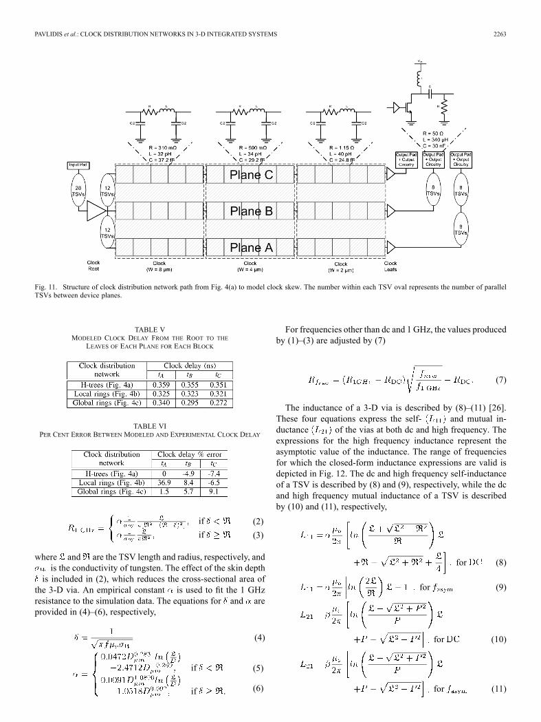
The electrical paths of the clock signal propagating from theroot to the leaves of each plane for the H-tree clock topology[see Fig. 4(a)] is depicted in Fig. 11. The size of the sourcefollower nMOS transistor and the dimensions of the clockbuffers at the root, leaves, and output circuitry are included inAppendix B. The clock network on each plane is composedof 50 m segments, where a -model represents the electricalproperties of each segment. These 50 m segments model thedistributive electrical properties of the interconnect. Similarly,when either meshes [see Fig. 4(b)] or rings [see Fig. 4(c)] areused on planes A and C (see Fig. 11), each 50 m segment isreplaced with an equivalent -model to more accurately repre-sent the single mesh and ring structure within the test circuit.Note that for the mesh structures, the clock signal is distributedto planes A and C from the leaves of the H-tree in plane B whilefor the rings topology, the clock signal distributed to planes Aand C is driven by buffers at the second level of the H-tree. Thedelay from the root to the leaves of each plane is included inTable V.The clock delays listed in Table V are compared with the
measured values listed in Table II. Good agreement betweenthe model and experimental data is shown. The per cent errorbetween the model and experimental clock delays is listed inTable VI. A maximum error of less than 10% is achieved for theclock paths within the H-tree topology. The larger errors shownin Table VI are due to the small time scale being examined.All of the values listed in Tables II and V are less than 550 ps;therefore, any small deviation in delay produces a large error.
VI. CONCLUSION
The design of a clock distribution network for applicationto 3-D circuits is considerably more complex than the de-sign of a 2-D clock distribution network. Three topologies toglobally distribute a clock signal within a 3-D circuit havebeen evaluated. A 3-D test circuit, based on the MITLL 3-DIC manufacturing process, has been designed, fabricated,and measured and is shown to operate at 1.4 GHz. Clockskew simulations incorporating both numerical simulationand analytic expressions produce comparable results to theexperimentally extracted clock skew measurements. The clockskew measurements indicate that a topology combining thesymmetry of an H-tree on the second plane and global ringson the remaining two planes results in low clock skew in 3-Dcircuits while consuming a moderate amount of power. Thisstructure, however, produces the largest root to leaf clock delayas compared to the other investigated topologies. Alternatively,for the H-tree and local rings topology, the lowest power isconsumed. The performance characteristics of these topologiessuggest that the target requirements should be considered whendesigning a 3-D clock distribution network.
APPENDIX AELECTRICAL PARAMETERS OF A THROUGH SILICON VIA
The resistance of a 3-D via [26] is
(1)
PAVLIDIS et al.: CLOCK DISTRIBUTION NETWORKS IN 3-D INTEGRATED SYSTEMS 2263
Fig. 11. Structure of clock distribution network path from Fig. 4(a) to model clock skew. The number within each TSV oval represents the number of parallelTSVs between device planes.
TABLE VMODELED CLOCK DELAY FROM THE ROOT TO THE
LEAVES OF EACH PLANE FOR EACH BLOCK
TABLE VIPER CENT ERROR BETWEEN MODELED AND EXPERIMENTAL CLOCK DELAY
if
if
(2)
(3)
where and are the TSV length and radius, respectively, andis the conductivity of tungsten. The effect of the skin depth
is included in (2), which reduces the cross-sectional area ofthe 3-D via. An empirical constant is used to fit the 1 GHzresistance to the simulation data. The equations for and areprovided in (4)–(6), respectively,
(4)
if
if .
(5)
(6)
For frequencies other than dc and 1 GHz, the values producedby (1)–(3) are adjusted by (7)
(7)
The inductance of a 3-D via is described by (8)–(11) [26].These four equations express the self- and mutual in-ductance of the vias at both dc and high frequency. Theexpressions for the high frequency inductance represent theasymptotic value of the inductance. The range of frequenciesfor which the closed-form inductance expressions are valid isdepicted in Fig. 12. The dc and high frequency self-inductanceof a TSV is described by (8) and (9), respectively, while the dcand high frequency mutual inductance of a TSV is describedby (10) and (11), respectively,
for (8)
for (9)
for (10)
for (11)
2264 IEEE TRANSACTIONS ON VERY LARGE SCALE INTEGRATION (VLSI) SYSTEMS, VOL. 19, NO. 12, DECEMBER 2011
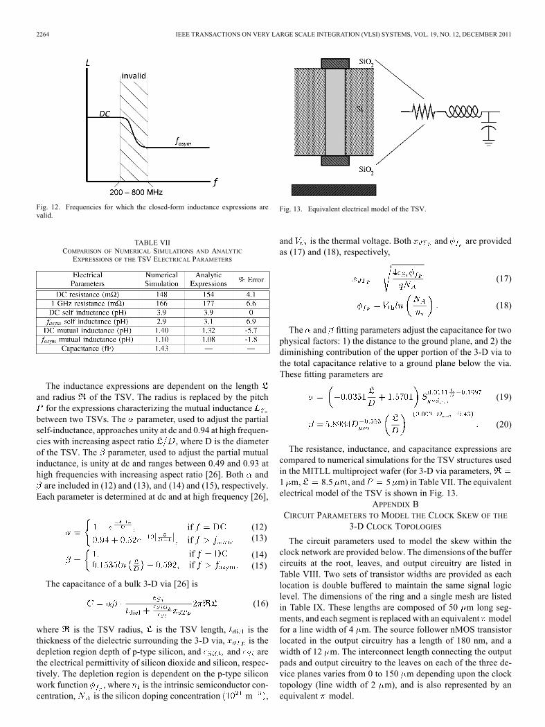
Fig. 12. Frequencies for which the closed-form inductance expressions arevalid.
TABLE VIICOMPARISON OF NUMERICAL SIMULATIONS AND ANALYTICEXPRESSIONS OF THE TSV ELECTRICAL PARAMETERS
The inductance expressions are dependent on the lengthand radius of the TSV. The radius is replaced by the pitchfor the expressions characterizing the mutual inductance
between two TSVs. The parameter, used to adjust the partialself-inductance, approaches unity at dc and 0.94 at high frequen-cies with increasing aspect ratio , where D is the diameterof the TSV. The parameter, used to adjust the partial mutualinductance, is unity at dc and ranges between 0.49 and 0.93 athigh frequencies with increasing aspect ratio [26]. Both andare included in (12) and (13), and (14) and (15), respectively.
Each parameter is determined at dc and at high frequency [26],
if
if
(12)(13)
ifif .
(14)(15)
The capacitance of a bulk 3-D via [26] is
(16)
where is the TSV radius, is the TSV length, is thethickness of the dielectric surrounding the 3-D via, is thedepletion region depth of p-type silicon, and and arethe electrical permittivity of silicon dioxide and silicon, respec-tively. The depletion region is dependent on the p-type siliconwork function , where is the intrinsic semiconductor con-centration, is the silicon doping concentration m ,
Fig. 13. Equivalent electrical model of the TSV.
and is the thermal voltage. Both and are providedas (17) and (18), respectively,
(17)
(18)
The and fitting parameters adjust the capacitance for twophysical factors: 1) the distance to the ground plane, and 2) thediminishing contribution of the upper portion of the 3-D via tothe total capacitance relative to a ground plane below the via.These fitting parameters are
(19)
(20)
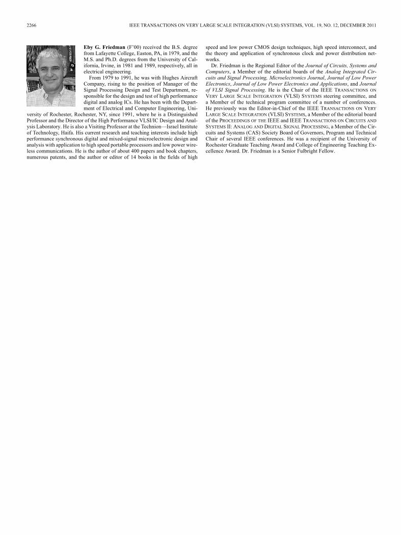
The resistance, inductance, and capacitance expressions arecompared to numerical simulations for the TSV structures usedin the MITLL multiproject wafer (for 3-D via parameters,1 m, 8.5 , and 5 m) in Table VII. The equivalentelectrical model of the TSV is shown in Fig. 13.
APPENDIX BCIRCUIT PARAMETERS TO MODEL THE CLOCK SKEW OF THE
3-D CLOCK TOPOLOGIES
The circuit parameters used to model the skew within theclock network are provided below. The dimensions of the buffercircuits at the root, leaves, and output circuitry are listed inTable VIII. Two sets of transistor widths are provided as eachlocation is double buffered to maintain the same signal logiclevel. The dimensions of the ring and a single mesh are listedin Table IX. These lengths are composed of 50 m long seg-ments, and each segment is replaced with an equivalent modelfor a line width of 4 m. The source follower nMOS transistorlocated in the output circuitry has a length of 180 nm, and awidth of 12 m. The interconnect length connecting the outputpads and output circuitry to the leaves on each of the three de-vice planes varies from 0 to 150 m depending upon the clocktopology (line width of 2 m), and is also represented by anequivalent model.

PAVLIDIS et al.: CLOCK DISTRIBUTION NETWORKS IN 3-D INTEGRATED SYSTEMS 2265
TABLE VIIITRANSISTOR WIDTH OF THE CLOCK BUFFERS AT THE ROOT, LEAVES, AND
OUTPUT CIRCUITRY (ALL LENGTHS ARE 180 nm)
TABLE IXDIMENSIONS OF LOCAL AND GLOBAL CLOCK RINGS
ACKNOWLEDGMENT
The authors would like to thank Y. Zhu, L. Zhang, and Prof.H. Wu of the University of Rochester for their help duringtesting and the MIT Lincoln Laboratories for fabricating the3-D test circuit.
REFERENCES
[1] Clock Distribution Networks in VLSI Circuits and Systems, E. G.Friedman, Ed.. Piscataway, NJ: IEEE Press, 1995.
[2] E. G. Friedman, “Clock distribution networks in synchronous digitalintegrated circuits,” Proc. IEEE, vol. 89, no. 5, pp. 665–692,May 2001.
[3] W. Bailey and B. J. Benschneider, “Clocking design and analysis fora 600-MHz alpha microprocessor,” IEEE J. Solid-State Circuits, vol.22, no. 11, pp. 1627–1633, Nov. 1998.
[4] T. Xanthopoulos, D. W. Bailey, A. K. Gangwar, M. K. Gowan, A. K.Jain, and B. K. Prewitt, “The design and analysis of the clock distribu-tion network for a 1.2 GHz alpha microprocessor,” in Proc. IEEE Int.Solid-State Circuits Conf., 2001, pp. 402–403.
[5] ScienceDaily, “3-D computer processor: “Rochester Cube” points wayto more powerful chip designs,” Sep. 17, 2008. [Online]. Available:www.sciencedaily.com/releases/2008/09/080915105733.htm
[6] V. F. Pavlidis, I. Savidis, and E. G. Friedman, “Clock distribution net-works for 3-D integrated circuits,” in Proc. IEEE Int. Conf. CustomIntegr. Circuits, 2008, pp. 651–654.
[7] V. F. Pavlidis, I. Savidis, and E. G. Friedman, “Clock distribution ar-chitectures for 3-D SOI integrated circuits,” in Proc. IEEE Int. Sil-icon-on-Insulator Conf., 2008, pp. 111–112.
[8] D. L. Lewis and H.-H. S. Lee, “A scan-island based design enablingpre-bond testability in die-stacked microprocessor,” in Proc. IEEE Int.Test Conf., 2007, pp. 21.2.1–21.2.8.
[9] W. R. Davis, J. Wilson, S. Mick, J. Xu, H. Hua, C. Mineo, A. M. Sule,M. Steer, and P. D. Franzon, “Demystifying 3D ICs: The pros and consof going vertical,” IEEEDes. Test Comput., vol. 22, no. 6, pp. 498–510,Nov./Dec. 2005.
[10] J. Minz, X. Zhao, and S. K. Lim, “Buffered clock tree synthesis for 3DICs under thermal variations,” in Proc. IEEE Int. Asia South PacificDes. Autom. Conf., 2008, pp. 504–509.
[11] M. Mondal, A. J. Ricketts, S. Kirolos, T. Ragheb, G. Link, N. Viyaykr-ishnan, and Y. Massoud, “Thermally robust clocking schemes for 3Dintegrated circuits,” in Proc. IEEE Int. Conf. Des., Autom. Test Euro.(DATE), 2007, pp. 1206–1211.
[12] V. Arunachalam and W. Burleson, “Low-power clock distribution ina multilayer core 3D microprocessor,” in Proc. ACM/IEEE Int. GreatLakes Symp. VLSI, 2008, pp. 429–434.
[13] “MITLL Low-Power FDSOI CMOS Process Design Guide,”MIT Lin-coln Laboratories, Cambridge, MA, 2006.
[14] J. A. Burns, B. F. Aull, C. K. Chen, C.-L. Chen, C. L. Keast, J. M.Knecht, V. Suntharalingam, K. Warner, P. W. Wyatt, and D.-R. W.Yost, “A wafer-scale 3-D circuit integration technology,” IEEE Trans.Electron Devices, vol. 53, no. 10, pp. 2507–2515, Oct. 2006.
[15] W. Cui, H. Chen, and Y. Han, “VLSI implemenation of universalrandom number generator,” in Proc. IEEE Asia-Pacific Conf. CircuitsSyst., 2002, pp. 465–470.
[16] M. Popovich, A. V. Mezhiba, and E. G. Friedman, Power Distribu-tion Networks With On-Chip Decoupling Capacitors. New York:Springer Verlag, 2008.
[17] N. Hedenstiema and K. O. Jeppson, “CMOS circuit speed and bufferoptimization,” IEEE Trans. Comput.-Aided Des. Integr. Circuits Syst.,vol. 6, no. 2, pp. 270–281, Mar. 1987.
[18] B. S. Cherkauer and E. G. Friedman, “A unified design methodologyfor CMOS tapered buffers,” IEEE Trans. Very Large Scale Integr.(VLSI) Syst., vol. 3, no. 1, pp. 99–111, Mar. 1995.
[19] H. B. Bakoglu, Circuits, Interconnections, and Packaging for VLSI.Boston, MA: Addison-Wesley, 1990.
[20] M. W. Newman, S. Muthukumar, M. Schuelein, T. Dambrauskas, P.A. Dunaway, J. M. Jordan, S. Kulkarni, C. D. Linde, T. A. Opheim, R.A. Stingel, W. Wormag, L. A. Topic, and J. M. Swan, “Fabrication andelectrical characterization of 3D vertical interconnects,” in Proc. IEEEInt. Electron. Components Technol. Conf., 2006, pp. 394–398.
[21] P. Dixit and J. Miao, “Fabrication of high aspect ratio 35 m pitch in-terconnects for next generation 3-D wafer level packaging by through-wafer copper electroplating,” in Proc. IEEE Int. Electron. ComponentsTechnol. Conf., 2006, pp. 388–393.
[22] K. Sugahara, T. Nishimura, S. Kusunoki, Y. Akasaka, and H. Nakata,“SOI/SOI/bulk-Si triple-level structure for three-dimensional devices,”IEEEElectronDevice Lett., vol. EDL-7, no. 3, pp. 193–194,Mar. 1986.
[23] A. Fan, A. Rahman, and R. Reif, “Copper wafer bonding,” Elec-trochem. Solid-State Lett., vol. 2, no. 10, pp. 534–536, Oct. 1999.
[24] A. W. Topol, D. C. Tulipe, L. L. Shi, D. J. Frank, K. Bernstein, S. E.Stein, A. Kumar, G. U. Singco, A. M. Young, K. W. Guarini, and M.Ieong, “Three-dimensional integrated circuits,” IBM J. Res. Develop-ment, vol. 50, no. 4/5, pp. 491–506, 2006.
[25] I. Savidis and E. G. Friedman, “Electrical modeling and characteriza-tion of 3-D vias,” in Proc. IEEE Int. Symp. Circuits Syst., 2008, pp.784–787.
[26] I. Savidis and E. G. Friedman, “Closed-form expressions of 3-D via re-sistance, inductance, and capacitance,” IEEE Trans. Electron Devices,vol. 56, no. 9, pp. 1873–1881, Sep. 2009.
Vasilis F. Pavlidis (M’09) received the B.S. andM.Eng. degrees in electrical and computer engi-neering from the Democritus University of Thrace,Xanthi, Greece, in 2000 and 2002, respectively, andthe M.Sc. and Ph.D. degrees from the Departmentof Electrical and Computer Engineering, Universityof Rochester, Rochester, NY, in 2003 and 2008,respectively.He is currently a post-doctoral researcher with the
Integrated Systems Laboratory, EPFL, Lausanne,Switzerland. From 2000 to 2002, he was with
INTRACOM S.A., Athens, Greece. In summer 2007, he was with SynopsysInc., Mountain View, CA. His current research interests include the area ofinterconnect modeling, 3-D integration, networks-on-chip, and related designissues in VLSI.
Ioannis Savidis received the B.S.E. degree in elec-trical and computer engineering and biomedical engi-neering fromDuke University, Durham, NC, in 2005,and the M.Sc. degree in electrical and computer engi-neering from the University of Rochester, Rochester,NY, in 2007, where he is currently pursuing the Ph.D.degree in electrical and computer engineering underthe guidance of Prof. E. G. Friedman.He interned at Freescale Semiconductor Corpora-
tion, Austin, TX, during the summers of 2006 and2007, where he worked on the electrical characteri-
zation and modeling of interplane 3-D vias. During the summers of 2008–2010,he interned at T. J.Watson Research Center, IBM,YorktownHeights, NY, wherehe worked on electrical characterization and modeling, reticle design, and DCand high frequency electrical measurements of test vehicles implementing var-ious interplane 3-D via topologies. His research interests include analysis, mod-eling, and design methodologies for high performance digital and mixed signalintegrated circuits, with an emphasis on electrical and thermal modeling andcharacterization, signal and power integrity, and power and clock delivery for3-D stacking technologies.
2266 IEEE TRANSACTIONS ON VERY LARGE SCALE INTEGRATION (VLSI) SYSTEMS, VOL. 19, NO. 12, DECEMBER 2011
Eby G. Friedman (F’00) received the B.S. degreefrom Lafayette College, Easton, PA, in 1979, and theM.S. and Ph.D. degrees from the University of Cal-ifornia, Irvine, in 1981 and 1989, respectively, all inelectrical engineering.From 1979 to 1991, he was with Hughes Aircraft
Company, rising to the position of Manager of theSignal Processing Design and Test Department, re-sponsible for the design and test of high performancedigital and analog ICs. He has been with the Depart-ment of Electrical and Computer Engineering, Uni-
versity of Rochester, Rochester, NY, since 1991, where he is a DistinguishedProfessor and the Director of the High Performance VLSI/IC Design and Anal-ysis Laboratory. He is also a Visiting Professor at the Technion—Israel Instituteof Technology, Haifa. His current research and teaching interests include highperformance synchronous digital and mixed-signal microelectronic design andanalysis with application to high speed portable processors and low power wire-less communications. He is the author of about 400 papers and book chapters,numerous patents, and the author or editor of 14 books in the fields of high
speed and low power CMOS design techniques, high speed interconnect, andthe theory and application of synchronous clock and power distribution net-works.Dr. Friedman is the Regional Editor of the Journal of Circuits, Systems and
Computers, a Member of the editorial boards of the Analog Integrated Cir-cuits and Signal Processing, Microelectronics Journal, Journal of Low PowerElectronics, Journal of Low Power Electronics and Applications, and Journalof VLSI Signal Processing. He is the Chair of the IEEE TRANSACTIONS ONVERY LARGE SCALE INTEGRATION (VLSI) SYSTEMS steering committee, anda Member of the technical program committee of a number of conferences.He previously was the Editor-in-Chief of the IEEE TRANSACTIONS ON VERYLARGE SCALE INTEGRATION (VLSI) SYSTEMS, a Member of the editorial boardof the PROCEEDINGS OF THE IEEE and IEEE TRANSACTIONS ON CIRCUITS ANDSYSTEMS II: ANALOG AND DIGITAL SIGNAL PROCESSING, a Member of the Cir-cuits and Systems (CAS) Society Board of Governors, Program and TechnicalChair of several IEEE conferences. He was a recipient of the University ofRochester Graduate Teaching Award and College of Engineering Teaching Ex-cellence Award. Dr. Friedman is a Senior Fulbright Fellow.