Embed Size (px)
Citation preview
Package
HALF-BRIDGE GATE DRIVER IC
Features• Floating channel up to +1200V• Soft overcurrent shutdown• Synchronization signal to synchronize shut down
with the other phases• Integrated desaturation detection circuit• Two stage turn on output for di/dt control• Separate pull-up/pull-down output drive pins• Matched delay outputs• Under voltage lockout with hysteresis band
www.irf.com 1
IR2214/IR22141
24-Lead SSOP
VOFFSET 1200V max.
IO+/- (typ.) 2.0 A / 3.0A
VOUT 10.4V - 20V
Deadtime matching (max) 75nsec
Deadtime (typ) 330nsec
Desat blanking time (typ) 3µsec DSH,DSL input voltage
threshold (typ) 8.0V Soft shutdown time (typ) 9.6µsec
Product Summary
DescriptionThe IR2214/IR22141 is a gate driver suited to drive asingle half bridge in power switching applications.The high gate driving capability (2A source, 3A sink)and the low quiescent current enable bootstrap supply techniques in mediumpower systems. The IR2214/IR22141 driver features full short circuit protectionby means of the power transistor desaturation detection. The IR2214/IR22141manages all the half-bridge faults by turning off smoothly the desaturated tran-sistor through the dedicated soft shut down pin, therefore preventing over-volt-ages and reducing EM emissions. In multi-phase system IR2214/IR22141 driv-ers communicate using a dedicated local network (SY_FLT and FAULT/SD sig-nals) to properly manage phase-to-phase short circuits. The system controllermay force shutdown or read device fault state through the 3.3 V compatible CMOSI/O pin (FAULT/SD). To improve the signal immunity from DC-bus noise, the con-trol and power ground usededicated pins enablinglow-side emitter currentsensing as well. Under volt-age conditions in floatingand low voltage circuits aremanaged independently.
Typical Connection
(Refer to Lead Assignments forcorrect pin configuration). This/These diagram(s) showelectrical connections only.Please refer to our ApplicationNotes and DesignTips forproper circuit board layout.
DC+
DC-
DC BUS(1200V)
VCC
LIN
HIN
FAULT/SD
VB
HOP
HON
SSDH
DSH
VS
LOP
LON
SSDL
DSL
COMVSS
IR22
14
FLT_CLR
SY_FLT
15 V
uP,Control
Motor
Data Sheet No. PD60213ADVANCE DATA

2
IR2214/IR22141
www.irf.com
ADVANCE DATA
Note 1: While internal circuitry is operational below the indicated supply voltages, the UV lockout disables the output drivers if the UV thresholds are not reached.Note 2: Logic operational for VS from VSS-5 to VSS+1200V. Logic state held for VS from VSS-5V to VSS-VBS. (Please refer to the Design Tip DT97-3 for more details).
Symbol Definition Min. Max. UnitsVB High side floating supply voltage (Note 1) VS + 11.5 VS + 20
VS High side floating supply offset voltage Note 2 1200
VHO High side output voltage (HOP, HON and SSDH) VS VS + 20
VLO Low side output voltage (LOP, LON and SSDL) VCOM VCC
VCC Low side and logic fixed supply voltage (Note 1) 11.5 20
COM Power ground - 5 5
VIN Logic input voltage (HIN, LIN and FLT_CLR) 0 VCC
VFLT Fault input/output voltage (FAULT/SD and SY_FLT) 0 VCC
VDSH High side DS pin input voltage VB - 20 VB
VDSL Low side DS pin input voltage VCC - 20 VCC
TA Ambient temperature -40 125 °C
Recommended Operating ConditionsFor proper operation the device should be used within the recommended conditions. All voltage parameters are absoutevoltages referenced to VSS. The VS offset rating is tested with all supplies biased at 15V differential.
V
Symbol Definition Min. Max. UnitsVS High side offset voltage VB - 25 VB + 0.3
VB High side floating supply voltage -0.3 1225
VHO High side floating output voltage (HOP, HON and SSDH) VS - 0.3 VB + 0.3
VCC Low side and logic fixed supply voltage -0.3 25
COM Power ground VCC - 25 VCC + 0.3
VLO Low side output voltage (LOP, LON and SSDL) VCOM -0.3 VCC + 0.3
VIN Logic input voltage (HIN, LIN and FLT_CLR) -0.3 VCC + 0.3
VFLT FAULT input/output voltage (FAULT/SD and SY_FLT) -0.3 VCC + 0.3
VDSH High side DS input voltage VB -25 VB + 0.3
VDSL Low side DS input voltage VCC - 25 VCC + 0.3
dVs/dt Allowable offset voltage slew rate — 50 V/ns
PD Package power dissipation @ TA ≤ +25°C — 1.5 W
RthJA Thermal resistance, junction to ambient — 65 °C/W
TJ Junction temperature — 150
TS Storage temperature -55 150
TL Lead temperature (soldering, 10 seconds) — 300
Absolute Maximum RatingsAbsolute maximum ratings indicate sustained limits beyond which damage to the device may occur. All voltage parametersare absolute voltages referenced to VSS, all currents are defined positive into any lead The thermal resistance and powerdissipation ratings are measured under board mounted and still air conditions.
V
°C
3
IR2214/IR22141
www.irf.com
ADVANCE DATA
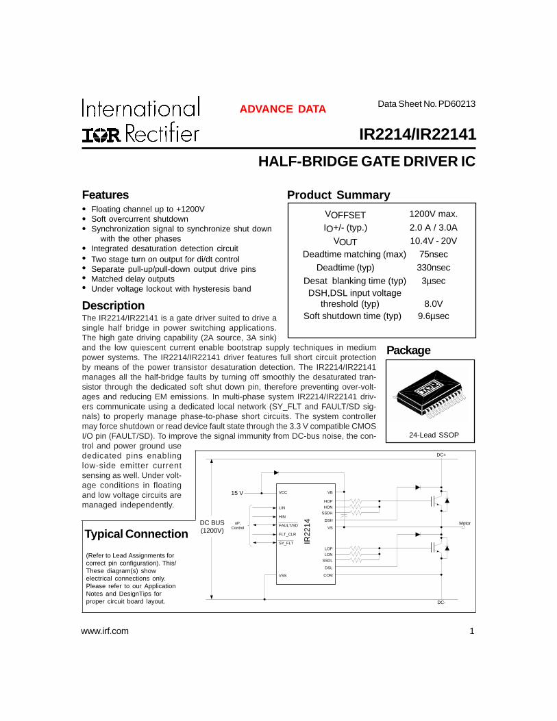
Pin: VCC, VSS, VB, VS Symbol Definition Min Typ Max Units Test Conditions
VCCUV+ Vcc supply undervoltage positive going threshold 9.3 10.2 11.4 VCCUV- Vcc supply undervoltage negative going threshold 8.7 9.3 10.3 VCCUVH Vcc supply undervoltage lockout hysteresis - 0.9 - VBSUV+ (VB-VS) supply undervoltage positive going threshold 9.3 10.2 11.4 VS=0V, VS=1200V VBSUV- (VB-VS) supply undervoltage negative going threshold 8.7 9.3 10.3 VS=0V, VS=1200V VBSUVH (VB-VS) supply undervoltage lockout hysteresis - 0.9 -
V
ILK Offset supply leakage current - - 50 VB = VS = 1200V
IQBS Quiescent VBS supply current - 400 800
VIN = 0V or 3.3V IQCC Quiescent Vcc supply current - 0.7 2.5 mA (No load)
VCC/VB
VCCUV/VBSUV
VSS/VS
comparator
UV internalsignal
Figure 1: Undervoltage diagram
HIN/LIN/FLTCLR
VSS
schmitttrigger
10k
internalsignal
Figure 2: HIN, LIN and FLTCLR diagram
µA
Static Electrical CharacteristicsVCC = 15 V, VSS = COM = 0 V, VS = 0 ÷ 1200 V and TA = 25 oC unless otherwise specified.
Pin: HIN, LIN, FLTCLR, FAULT/SD, SY_FLTSymbol Definition Min Typ Max Units Test Conditions
VIH Logic "1" input voltage 2.0 - - VIL Logic "0" input voltage - - 0.8
VIHSS Logic input hysteresis 0.2 0.4 -
V VCC = VCCUV- to
20V
IIN+ Logic "1" input bias current - 370 - VIN = 3.3V IIN- Logic "0" input bias current -1 - 0 VIN = 0V
RON,FLT FAULT/SD open drain resistance - 60 -
RON,SY SY_FLT open drain resistance - 60 -
P ÿ≤ 7
4
IR2214/IR22141
www.irf.com
ADVANCE DATA
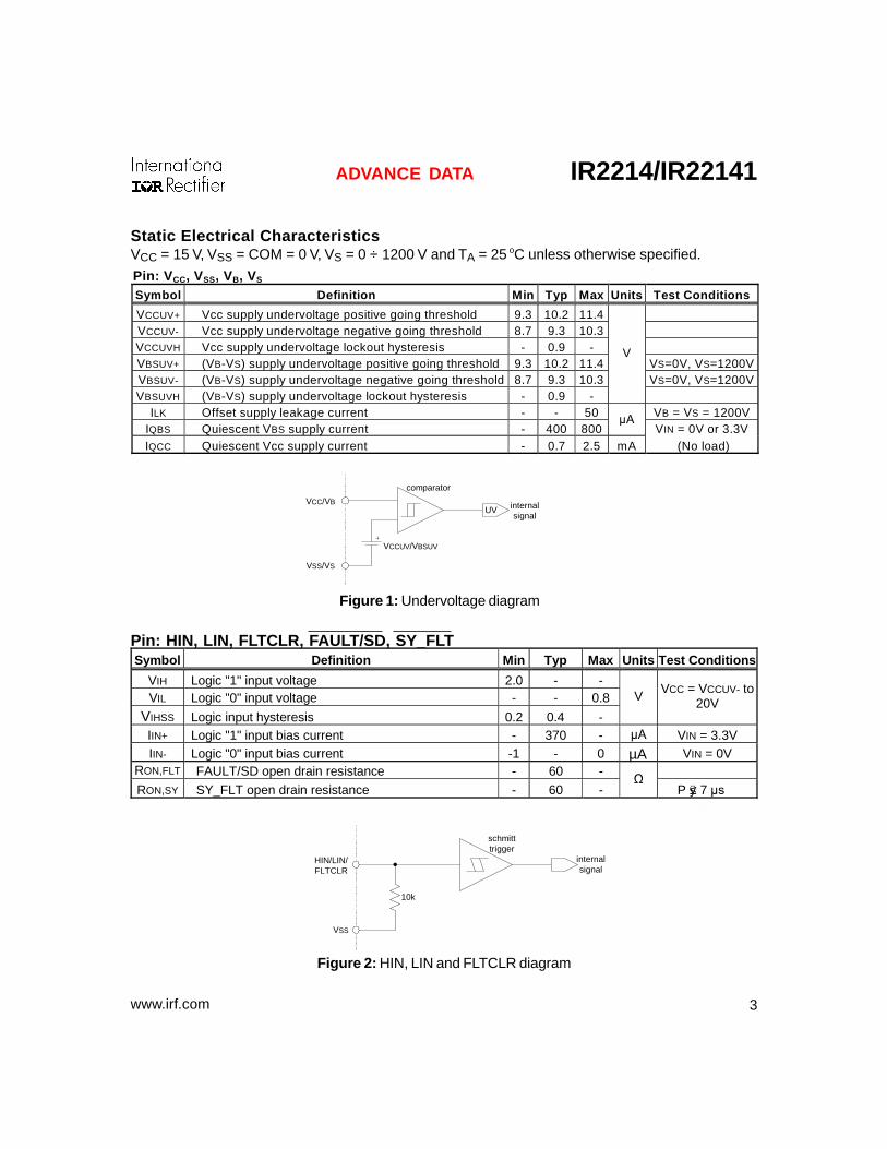
The active bias is present only in IR22141. VDESAT, IDS and IDSB parameters are referenced to COM and VS respectively for DSL and DSH.
Symbol Definition Min Typ Max Units Test Conditions
VDESAT+ High desat input threshold voltage 7.2 8.0 8.8 VDESAT- Low desat input threshold voltage 6.3 7.0 7.7 VDSTH Desat input voltage hysteresis - 1.0 -
V See Fig. 16, 4
IDS+ High DSH or DSL input bias current - 21 - VDESAT = VCC or VBS IDS- Low DSH or DSL input bias current - -160 -
VDESAT = 0V
IDSB DSH or DSL input bias current (IR22141 only) - -20 - mA VDESAT = (VCC or VBS) - 2V
Pin: DSL, DSH
DSL/DSH
VDESAT
COM/VS
comparator
100k
700k
VCC/VBS
SSDinternalsignal
activebias
Figure 4: DSH and DSL diagram
FAULT/SDSY_FLT
VSS
schmitttrigger
R ON
fault/holdinternal signal
hard/soft shutdowninternal signal
Figure 3: FAULT/SD and SY_FLT diagram
5
IR2214/IR22141
www.irf.com
ADVANCE DATA
Symbol Definition Min Typ Max Units Test Conditions
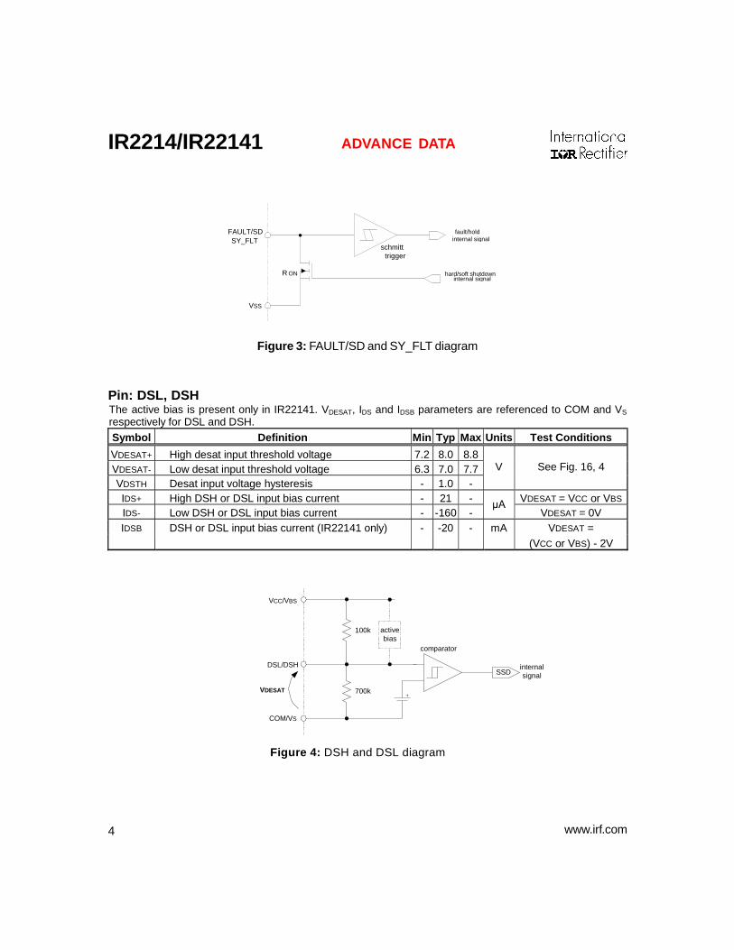
VOH High level output voltage, VB – VHOP or Vcc –VLOP - 20 100 mV IO = 1mA IO1+ Output high first stage short circuit pulsed current - 2 -
VHOP/LOP=0V, HIN or LIN= 1, PW≤200ns,
resistive load, see Fig. 8
IO2+ Output high second stage short circuit pulsed current
- 1 - A
VHOP/LOP=0V, HIN or LIN = 1,
400ns≤PW≤10resistive load,
see Fig. 8
Pin: HOP, LOP
LOP/HOP
VCC/VB
on/offinternal signal
VOH
200nsoneshot
Figure 5: HOP and LOP diagram
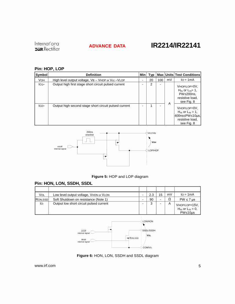
SSDL/SSDH
COM/VS
on/offinternal signal
RON,SSD
LON/HON
desatinternal signal
VOL
Figure 6: HON, LON, SSDH and SSDL diagram
VOL Low level output voltage, VHON or VLON - 2.3 15 mV IO = 1mA
RON,SSD Soft Shutdown on resistance (Note 1) - 90 - PW ≤ 7 IO- Output low short circuit pulsed current - 3 - A VHOP/LOP=15V,
HIN or LIN = 0, PW≤10
Pin: HON, LON, SSDH, SSDL
6
IR2214/IR22141
www.irf.com
ADVANCE DATA
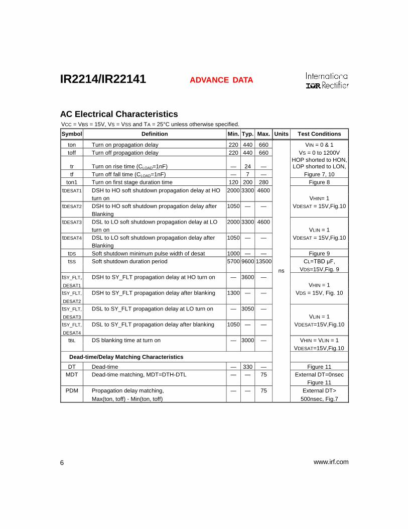
AC Electrical Characteristics VCC = VBS = 15V, VS = VSS and TA = 25°C unless otherwise specified.
Symbol Definition Min. Typ. Max. Units Test Conditions
ton Turn on propagation delay 220 440 660 VIN = 0 & 1 toff Turn off propagation delay 220 440 660 VS = 0 to 1200V
tr Turn on rise time (CLOAD=1nF) — 24 — HOP shorted to HON, LOP shorted to LON,
tf Turn off fall time (CLOAD=1nF) — 7 — Figure 7, 10 ton1 Turn on first stage duration time 120 200 280 Figure 8
tDESAT1 DSH to HO soft shutdown propagation delay at HO 2000 3300 4600 turn on VHIN= 1
tDESAT2 DSH to HO soft shutdown propagation delay after 1050 — — VDESAT = 15V,Fig.10 Blanking
tDESAT3 DSL to LO soft shutdown propagation delay at LO 2000 3300 4600 turn on VLIN = 1
tDESAT4 DSL to LO soft shutdown propagation delay after 1050 — — VDESAT = 15V,Fig.10 Blanking
tDS Soft shutdown minimum pulse width of desat 1000 — — Figure 9 tSS Soft shutdown duration period 5700 9600 13500 CL VDS=15V,Fig. 9
tSY_FLT, DSH to SY_FLT propagation delay at HO turn on — 3600 — DESAT1 VHIN = 1 tSY_FLT, DSH to SY_FLT propagation delay after blanking 1300 — — VDS = 15V, Fig. 10 DESAT2 tSY_FLT, DSL to SY_FLT propagation delay at LO turn on — 3050 — DESAT3 VLIN = 1 tSY_FLT, DSL to SY_FLT propagation delay after blanking 1050 — — VDESAT=15V,Fig.10 DESAT4
tBL DS blanking time at turn on — 3000 — VHIN = VLIN = 1 VDESAT=15V,Fig.10
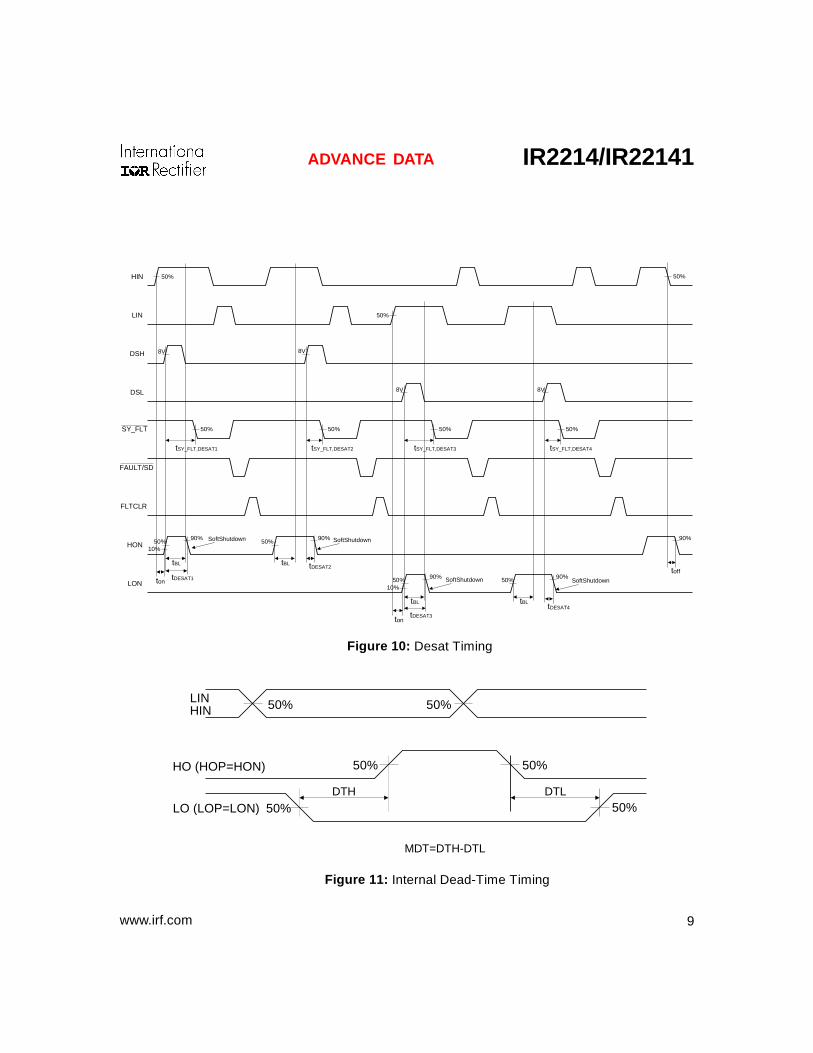
Dead-time/Delay Matching Characteristics DT Dead-time — 330 — Figure 11
MDT Dead-time matching, MDT=DTH-DTL — — 75 External DT=0nsec Figure 11
PDM Propagation delay matching, — — 75 External DT>
Max(ton, toff) - Min(ton, toff)
ns
500nsec, Fig.7

7
IR2214/IR22141
www.irf.com
ADVANCE DATA
HINLIN
HO (HOP=HON)LO (LOP=LON)
10%
3.3V
10%
90% 90%
50% 50%
trton toff tf
PWin
PWout
Figure 7: Switching Time Waveforms
Ton1
Io1+
Io2+
Figure 8: Output Source Current

8
IR2214/IR22141
www.irf.com
ADVANCE DATA
HIN/LIN
HO/LO
VDESAT+ VDESAT-
tSStDESAT
3.3V
DSH/DSL
tDS
SSD Driver Enable
Figure 9: Soft Shutdown Timing Waveform
9
IR2214/IR22141
www.irf.com
ADVANCE DATA
HIN
DSH
SY_FLT
HON
FAULT/SD
FLTCLR
LIN
LON
DSL
50%50%
50%
8V8V
8V 8V
50% 50% 50% 50%
50%90% 90%
50%10%
90%
50% 90%
10%
90%50%ton
tBL
SoftShutdown
tDESAT1
tSY_FLT,DESAT1
tBL tDESAT2
tSY_FLT,DESAT2
SoftShutdown
ton
tBL
tDESAT3
tSY_FLT,DESAT3
SoftShutdown
tBLtDESAT4
SoftShutdown
tSY_FLT,DESAT4
toff
Figure 10: Desat Timing
HINLIN
HO (HOP=HON)
LO (LOP=LON)DTH DTL
50%
50%
50% 50%
50%
MDT=DTH-DTL
50%
Figure 11: Internal Dead-Time Timing
10
IR2214/IR22141
www.irf.com
ADVANCE DATA
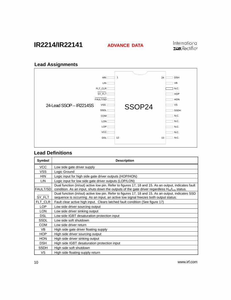
Symbol Description
VCC Low side gate driver supply VSS Logic Ground HIN Logic input for high side gate driver outputs (HOP/HON) LIN Logic input for low side gate driver outputs (LOP/LON)
FAULT/SD
Dual function (in/out) active low pin. Refer to figures 17, 18 and 15. As an output, indicates fault condition. As an input, shuts down the outputs of the gate driver regardless HIN/LIN status.
SY_FLT
Dual function (in/out) active low pin. Refer to figures 17, 18 and 15. As an output, indicates SSD sequence is occurring. As an input, an active low signal freezes both output status.
FLT_CLR Fault clear active high input. Clears latched fault condition (See figure 17) LOP Low side driver sourcing output LON Low side driver sinking output DSL Low side IGBT desaturation protection input
SSDL Low side soft shutdown COM Low side driver return VB High side gate driver floating supply
HOP High side driver sourcing output HON High side driver sinking output DSH High side IGBT desaturation protection input
SSDH High side soft shutdown VS High side floating supply return
Lead Definitions
SSOP24
1
12
24
13
SSDL
FLT_CLR
HIN
COM
SY_FLT
LON
FAULT/SD
VSS
LOP
VCC
DSL
HOP
SSDH
HON
N.C.
VS
N.C.
DSH
VB
N.C.
N.C.
N.C.
N.C.
LIN
24-Lead SSOP – IR2214SS
Lead Assignments
11
IR2214/IR22141
www.irf.com
ADVANCE DATA
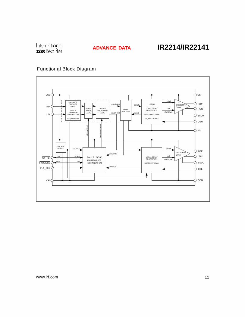
Functional Block Diagram
SCHMITTTRIGGER
INPUT
SHOOTTHROUGH
PREVENTION
(DT) Deadtime
LEVELSHIFTERS
LATCH
LOCAL DESATPROTECTION
SOFT SHUTDOWN
UV_VBS DETECT
di/dt controlDriver
UV_VCCDETECT
LOCAL DESATPROTECTION
SOFTSHUTDOWN
di/dt controlDriver
on/off
on/off
desat
soft
shutdown
on/off
soft
shutdown
on/off (HS)
DesatHS
DesatLS
on/off (LS)
Har
d S
hutD
own
inte
rnal
Hol
d
SD
FAULT LOGICmanagemend(See figure 14)
UV_VCC
VB
HOP
HON
SSDH
DSH
VS
LOP
LON
SSDL
DSL
COMVSS
FLT_CLR
FAULT/SD
SY_FLT
LIN
HIN
VCC
FAULT
HOLDSSD
INPUTHOLDLOGIC
OUTPUTSHUTDOWN
LOGIC
12
IR2214/IR22141
www.irf.com
ADVANCE DATA
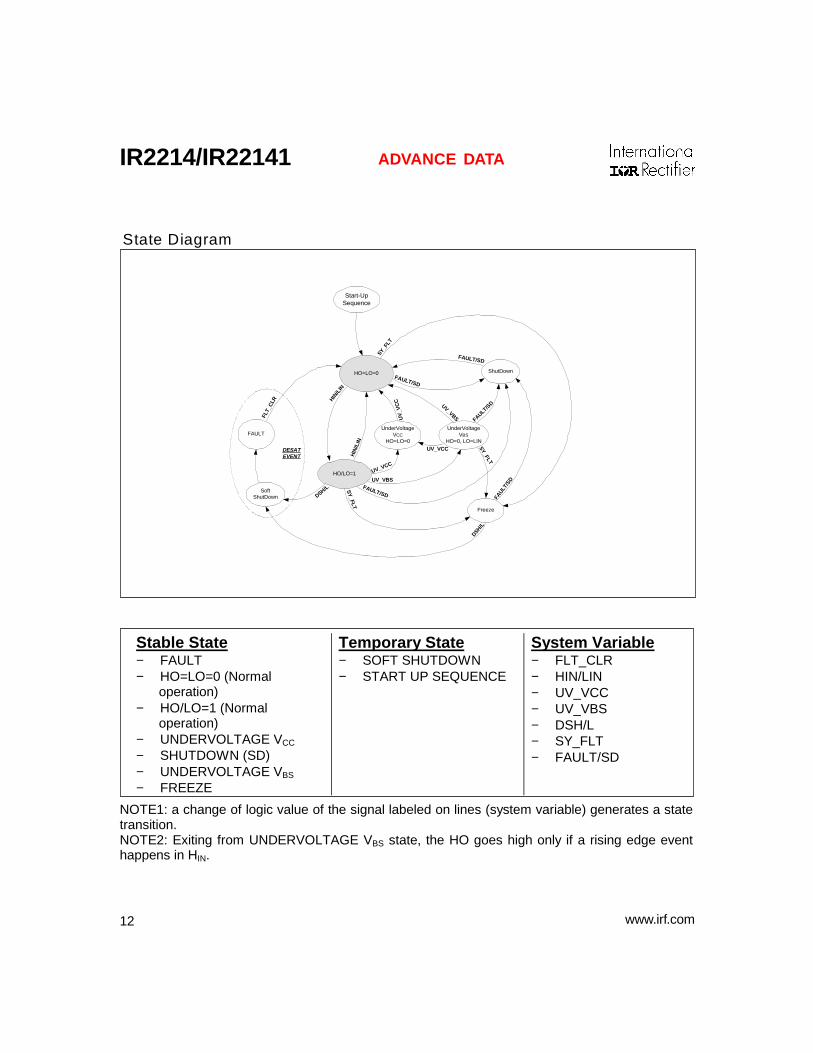
NOTE1: a change of logic value of the signal labeled on lines (system variable) generates a state transition. NOTE2: Exiting from UNDERVOLTAGE VBS state, the HO goes high only if a rising edge event happens in HIN.
Stable State − FAULT − HO=LO=0 (Normal
operation) − HO/LO=1 (Normal
operation) − UNDERVOLTAGE VCC − SHUTDOWN (SD) − UNDERVOLTAGE VBS − FREEZE
Temporary State − SOFT SHUTDOWN − START UP SEQUENCE
System Variable − FLT_CLR − HIN/LIN − UV_VCC − UV_VBS − DSH/L − SY_FLT − FAULT/SD
Start-UpSequence
FAULT
HO/LO=1
HO=LO=0
UnderVoltageVCC
HO=LO=0
Freeze
ShutDownSY
_FLT
SY
_FLT
SY_FLT
FLT_
CLR HIN
/LIN
HIN
/LIN
UV_VCC
UV
_VC
C
UV_VBSFAULT/SDDSH/L
DSH/L
FAULT
/SD
FAULT/SD
FAULT/SD
FAULT/S
DUV_VBS
UV_VCCDESATEVENT
UnderVoltageVBS
HO=0, LO=LIN
SoftShutDown
State Diagram
13
IR2214/IR22141
www.irf.com
ADVANCE DATA
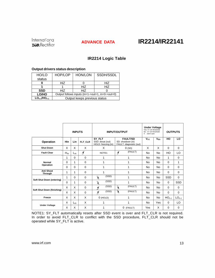
HO/LO status
HOP/LOP HON/LON SSDH/SSDL
0 HiZ 0 HiZ 1 1 HiZ HiZ
SSD HiZ HiZ 0 LO/HO Output follows inputs (in=1->out=1, in=0->out=0)
LOn-1/HOn-1 Output keeps previous status
IR2214 Logic Table
NOTE1: SY_FLT automatically resets after SSD event is over and FLT_CLR is not required. In order to avoid FLT_CLR to conflict with the SSD procedure, FLT_CLR should not be operated while SY_FLT is active.
INPUTS
INPUT/OUTPUT
Under Voltage Yes: V< UV threshold No : V> UV threshold X : don’t care
OUTPUTS
Hin
Lin
FLT_CLR
SY_FLT SSD: desat (out) HOLD: freezing (in)
FAULT/SD SD: shutdown (in) FAULT: diagnostic (out)
VCC VBS HO LO
X X X X 0 (SD) X X 0 0
HIN LIN NOTE1 (FAULT) No No HO LO
1 0 0 1 1 No No 1 0
0 1 0 1 1 No No 0 1
0 0 0 1 1 No No 0 0
1 1 0 1 1 No No 0 0
1 0 0 (SSD) 1 No No SSD 0
0 1 0 (SSD) 1 No No 0 SSD
X X 0 (SSD) (FAULT) No No 0 0
X X 0 (SSD) (FAULT) No No 0 0
X X X 0 (HOLD) 1 No No HOn-1 LOn-1
X LIN X 1 1 No Yes 0 LO
X X X 1 0 (FAULT) Yes X 0 0
Normal
Operation
Anti Shoot Through
Soft Shut Down (entering)
Soft Shut Down (finishing)
Freeze
Shut Down
Fault Clear
Operation
Under Voltage
Output drivers status description
14
IR2214/IR22141
www.irf.com
ADVANCE DATA
FEATURES DESCRIPTION
1. Start-up sequenceAt power supply start-up it is recommended tokeep FLT_CLR pin active until supply voltagesare properly established. This prevents spuriousdiagnostic signals being generated. All protectionfunctions are operating independently fromFLT_CLR status and output driver status reflectsthe input commands.When bootstrap supply topology is used forsupplying the floating high side stage, thefollowing start-up sequence is recommended(see also figure 12):
1. Set Vcc2. Set FLT_CLR pin to HIGH level3. Set LIN pin to HIGH level and let the
bootstrap capacitor be charged4. Release LIN pin to LOW level
5. Release FLT_CLR pin to LOW level
Figure 12 Start-up sequence
A minimum 15µs LIN and FLT-CLR pulse isrequired.
VCC
FLT_CLR
LIN
LO
2. Normal operation modeAfter start-up sequence has been terminated, thedevice becomes fully operative (see grey blocksin the State Diagram).HIN and LIN produce driver outputs to switchaccordingly, while the input logic checks the inputsignals preventing shoot-through events andincluding DeadTime (DT).
3. Shut downThe system controller can asynchronouslycommand the Hard ShutDown (HSD) through the3.3 V compatible CMOS I/O FAULT/SD pin. Thisevent is not latched.In a multi-phase system, FAULT/SD signals areor-wired so the controller or one of the gate driverscan force simultaneous shutdown to the othergate drivers through the same pin.
4. Fault managementIR2214 is able to manage both the supply failure(undervoltage lock out on both low and high sidecircuits) and the desaturation of both powertransistors.
4.1 Undervoltage (UV)The Undervoltage protection function disables thedriver’s output stage preventing the power devicebeing driven with too low voltages.Both the low side (V
CC supplied) and the floating
side (VBS
supplied) are controlled by a dedicateundervoltage function.Undervoltage event on the V
CC (when
VCC
< UVVCC-
) generates a diagnostic signal byforcing FAULT/SD pin low (see FAULT/SD sectionand figure 14). This event disables both low sideand floating drivers and the diagnostic signal holdsuntil the under voltage condition is over. Faultcondition is not latched and the FAULT/SD pin isreleased once V
CC becomes higher than UV
VCC+.
15
IR2214/IR22141
www.irf.com
ADVANCE DATA
The undervoltage on the VBS works disabling onlythe floating driver. Undervoltage on VBS does notprevent the low side driver to activate its outputnor generate diagnostic signals. VBS undervoltagecondition (VBS < UVVBS-) latches the high sideoutput stage in the low state. VBS must bereestablished higher than UVVBS+ to return innormal operating mode. To turn on the floatingdriver HIN must be re-asserted high (rising edgeevent on HIN is required).
4.2 Power devices desaturationDifferent causes can generate a power inverterfailure: phase and/or rail supply short-circuit,overload conditions induced by the load, etc…In all these fault conditions a large currentincrease is produced in the IGBT.The IR2214 fault detection circuit monitors theIGBT emitter to collector voltage (V
CE) by means
of an external high voltage diode. High current inthe IGBT may cause the transistor to desaturate,i.e. V
CE to increase.
Once in desaturation, the current in powertransistor can be as high as 10 times the nominalcurrent. Whenever the transistor is switched off,this high current generates relevant voltagetransients in the power stage that need to besmoothed out in order to avoid destruction (byover-voltages). The IR2214 gate driver accomplishthe transients control by smoothly turning off thedesaturated transistor by means of the SSD pinactivating a so called Soft ShutDown sequence(SSD).
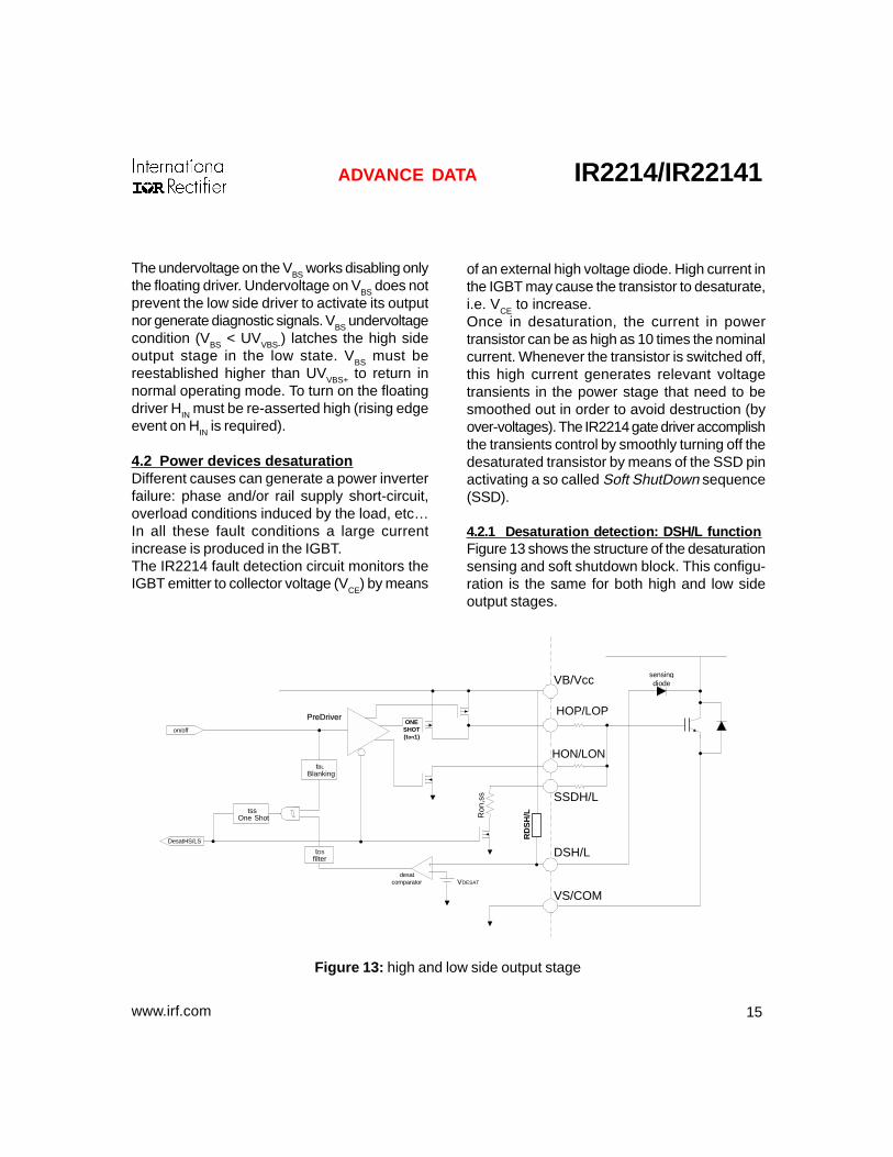
4.2.1 Desaturation detection: DSH/L functionFigure 13 shows the structure of the desaturationsensing and soft shutdown block. This configu-ration is the same for both high and low sideoutput stages.
Figure 13: high and low side output stage
tBL
Blanking
VB/Vcc
HON/LON
DSH/L
VS/COM
Ron
,ss
HOP/LOP
tssOne Shot
VDESAT
(ton1)
ONESHOT
tDSfilter
SSDH/L
RD
SH
/L
PPrreeDDrriivveerr
sensingdiode
on/off
DesatHS/LS
desatcomparator

16
IR2214/IR22141
www.irf.com
ADVANCE DATA
FLTCLR
Q
QSET
CLR
S
R
FAULT/SD
SY_FLT
internal HOLD
(externalhold)
(external hardshutdown)
internal FAULT (hard shutdown)
UVCC
DesatHS
DesatLS
Figure 14: fault management diagram
The external sensing diode should haveBV>1200V and low stray capacitance (in orderto minimize noise coupling and switching de-lays). The diode is biased by an internal pull-upresistor R
DSH/L (equal to V
CC/I
DS- or V
BS/I
DS- for
IR2214) or by a dedicated circuit (see the active-bias section for the IR22141). When V
CE in-
creases, the voltage at DSH/L pin increases too.Being internally biased to the local supply,DSH/L voltage is automatically clamped. WhenDSH/L exceeds the V
DESAT+ threshold the com-
parator triggers (see figure 13). Comparatoroutput is fi ltered in order to avoid falsedesaturation detection by externally inducednoise; pulses shorter than t
DS are filtered out. To
avoid detecting a false desaturation during IGBTturn on, the desaturation circuit is disabled by aBlanking signal (T
BL, see Blanking block in fig-
ure 13). This time is the estimated maximumIGBT turn on time and must be not exceeded byproper gate resistance sizing. When the IGBT is
not completely saturated after TBL
, desaturationis detected and the driver will turn off.Eligible desaturation signals initiate the SoftShutdown sequence (SSD). While in SSD, theoutput driver goes in high impedance and theSSD pull-down is activated to turn off the IGBTthrough SSDH/L pin. The SY_FLT output pin(active low, see figure 14) reports the IR2214status all the way long SSD sequence lasts (t
SS).
Once finished SSD, SYS_FLT releases, andIR2214 generates a FAULT signal (see theFAULT/SD section) by activating FAULT/SD pin.This generates a hard shut down for both highand low output stages (HO=LO=low). Each driveris latched low until the fault is cleared (seeFLT_CLR).Figure 14 shows the fault management circuit.In this diagram DesatHS and DesatLS are twointernal signals that come from the output stages(see figure 13).
17
IR2214/IR22141
www.irf.com
ADVANCE DATA
It must be noted that while in Soft Shut Down,both Under Voltage fault and external Shut Down(SD) are masked until the end of SSD.Desaturation protection is working independentlyby the other entire control pin and it is disabledonly when the output status is off.
VCC
LIN
HIN
FLT_CLR
VB
HOP
HON
SSH
DSH
VS
LOP
LON
SSL
DSL
COMVSS
SY_FLT
FAULT/SD
IR22
14
VCC
LIN
HIN
FLT_CLR
VB
HOP
HON
SSH
DSH
VS
LOP
LON
SSL
DSL
COMVSS
SY_FLT
FAULT/SD
IR22
14
VCC
LIN
HIN
FLT_CLR
VB
HOP
HON
SSH
DSH
VS
LOP
LON
SSL
DSL
COMVSS
SY_FLT
FAULT/SD
IR22
14
phase U phase V phase W
FAULT
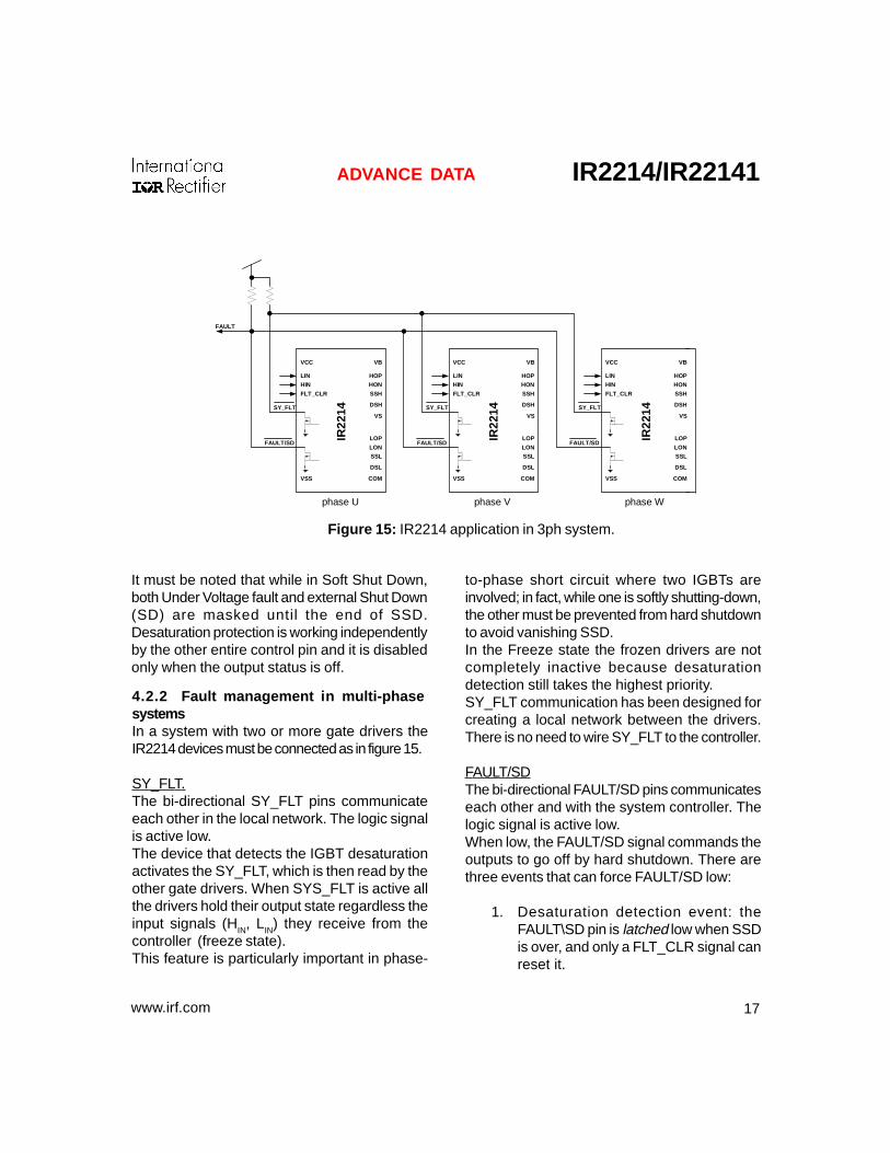
4.2.2 Fault management in multi-phasesystemsIn a system with two or more gate drivers theIR2214 devices must be connected as in figure 15.
SY_FLT.The bi-directional SY_FLT pins communicateeach other in the local network. The logic signalis active low.The device that detects the IGBT desaturationactivates the SY_FLT, which is then read by theother gate drivers. When SYS_FLT is active allthe drivers hold their output state regardless theinput signals (H
IN, L
IN) they receive from the
controller (freeze state).This feature is particularly important in phase-
to-phase short circuit where two IGBTs areinvolved; in fact, while one is softly shutting-down,the other must be prevented from hard shutdownto avoid vanishing SSD.In the Freeze state the frozen drivers are notcompletely inactive because desaturationdetection still takes the highest priority.SY_FLT communication has been designed forcreating a local network between the drivers.There is no need to wire SY_FLT to the controller.
FAULT/SDThe bi-directional FAULT/SD pins communicateseach other and with the system controller. Thelogic signal is active low.When low, the FAULT/SD signal commands theoutputs to go off by hard shutdown. There arethree events that can force FAULT/SD low:
1. Desaturation detection event: theFAULT\SD pin is latched low when SSDis over, and only a FLT_CLR signal canreset it.
Figure 15: IR2214 application in 3ph system.
18
IR2214/IR22141
www.irf.com
ADVANCE DATA
2. Undervoltage on VCC
: the FAULT\SD pinis forced low and held until theundervoltage is active (not latched).
3. FAULT/SD is externally driven low eitherfrom the controller or from anotherIR2214 device. This event is not latched;therefore the FLT_CLR cannot disableit. Only when FAULT/SD becomes highthe device returns in normal operatingmode.
5. Active biasFor the purpose of sensing the power transistordesaturation the collector voltage is read by anexternal HV diode. The diode is normally biasedby an internal pull up resistor connected to thelocal supply line (V
B or V
CC). When the transistor
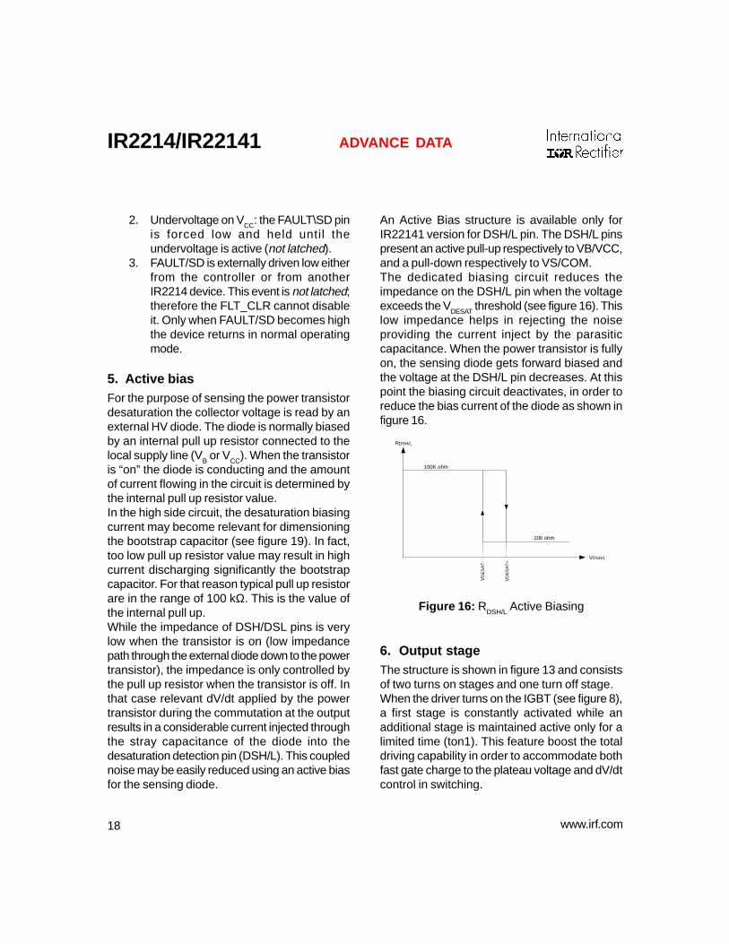
is “on” the diode is conducting and the amountof current flowing in the circuit is determined bythe internal pull up resistor value.In the high side circuit, the desaturation biasingcurrent may become relevant for dimensioningthe bootstrap capacitor (see figure 19). In fact,too low pull up resistor value may result in highcurrent discharging significantly the bootstrapcapacitor. For that reason typical pull up resistorare in the range of 100 kΩ. This is the value ofthe internal pull up.While the impedance of DSH/DSL pins is verylow when the transistor is on (low impedancepath through the external diode down to the powertransistor), the impedance is only controlled bythe pull up resistor when the transistor is off. Inthat case relevant dV/dt applied by the powertransistor during the commutation at the outputresults in a considerable current injected throughthe stray capacitance of the diode into thedesaturation detection pin (DSH/L). This couplednoise may be easily reduced using an active biasfor the sensing diode.
An Active Bias structure is available only forIR22141 version for DSH/L pin. The DSH/L pinspresent an active pull-up respectively to VB/VCC,and a pull-down respectively to VS/COM.The dedicated biasing circuit reduces theimpedance on the DSH/L pin when the voltageexceeds the V
DESAT threshold (see figure 16). This
low impedance helps in rejecting the noiseproviding the current inject by the parasiticcapacitance. When the power transistor is fullyon, the sensing diode gets forward biased andthe voltage at the DSH/L pin decreases. At thispoint the biasing circuit deactivates, in order toreduce the bias current of the diode as shown infigure 16.
Figure 16: RDSH/L
Active Biasing
6. Output stageThe structure is shown in figure 13 and consistsof two turns on stages and one turn off stage.When the driver turns on the IGBT (see figure 8),a first stage is constantly activated while anadditional stage is maintained active only for alimited time (ton1). This feature boost the totaldriving capability in order to accommodate bothfast gate charge to the plateau voltage and dV/dtcontrol in switching.
VDSH/L
VD
ES
AT
-
VD
ES
AT
+
100 ohm
100K ohm
RDSH/L

19
IR2214/IR22141
www.irf.com
ADVANCE DATA
At turn off, a single n-channel sinks up to 3A (I )O-
and offers a low impedance path to prevent theself-turn on due to the parasitic Miller capacitancein the power switch.
HIN
LIN
FAULT/SD
LO(LOP/LON)
DSH
FLT_CLR
SY_FLT
HO(HOP/HON)
DSL
A B C D E F G
Figure 17: I/O timing diagram with SY_FLT and FAULT/SD as output
7. Timing and logic state diagramsdescriptionThe following figures show the input/output logicdiagram.Figure 17 shows the SY_FLT and FAULT/SDsignals as output, whereas figure 18 shows themas input.

20
IR2214/IR22141
www.irf.com
ADVANCE DATA
A B C D E F
HIN
LIN
SY_FLT
FAULT/SD
FLT_CLR
HO (HOP/HON)
LO (LOP/LON)
Figure 18: I/O logic diagram with SY_FLT and FAULT/SD as input
Referred to timing diagram of figure 17:A. When the input signals are on together the
outputs go off (anti-shoot through).B. The HO signal is on and the high side IGBT
desaturates, the HO turn off softly while theSY_FLT stays low. When SY_FLT goes highthe FAULT/SD goes low. While in SSD, ifLIN goes up, LO does not change (freeze).
C. When FAULT/SD is latched low (see FAULT/SD section) FLT_CLR can disable it and theoutputs go back to follow the inputs.
D. The DSH goes high but this is not readbecause HO is off.
E. The LO signal is on and the low side IGBTdesaturates, the low side behaviour is thesame as described in point B.
F. The DSL goes high but this is not readbecause LO is off.
G. As point A (anti-shoot through).
Referred to logic diagram figure 18:A. The device is in hold state, regardless of input
variations. Hold state is forced by SY_FLTforced low externally
B. The device outputs goes off by hardshutdown, externally commanded. A throughB is the same sequence adopted by anotherIR2214 device in SSD procedure.
C. Externally driven low FAULT/SD (shutdownstate) cannot be disabled by forcing FLT_CLR(see FAULT/SD section).
D. The FAULT/SD is released and the outputsgo back to follow the inputs.
E. Externally driven low FAULT/SD: outputs gooff by hard shutdown (like point B).
F. As point A and B but for the low side output.
21
IR2214/IR22141
www.irf.com
ADVANCE DATA
Sizing tips
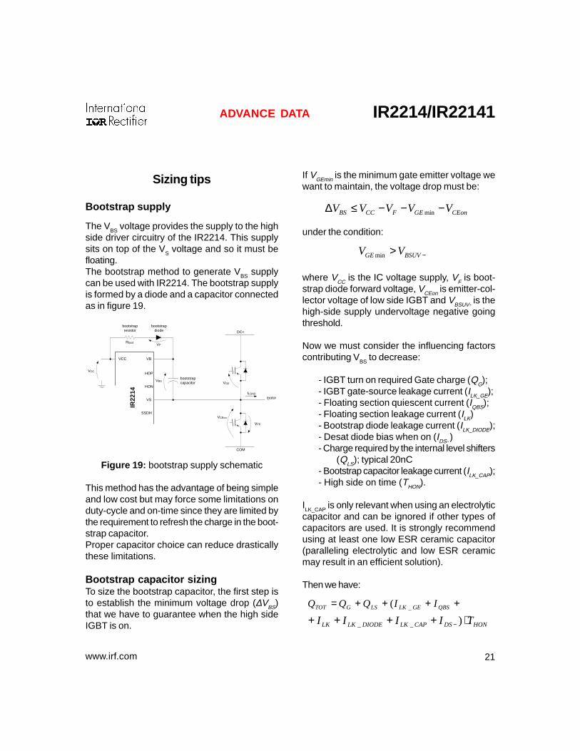
Bootstrap supply
The VBS
voltage provides the supply to the highside driver circuitry of the IR2214. This supplysits on top of the V
S voltage and so it must be
floating.The bootstrap method to generate V
BS supply
can be used with IR2214. The bootstrap supplyis formed by a diode and a capacitor connectedas in figure 19.
Figure 19: bootstrap supply schematic
This method has the advantage of being simpleand low cost but may force some limitations onduty-cycle and on-time since they are limited bythe requirement to refresh the charge in the boot-strap capacitor.Proper capacitor choice can reduce drasticallythese limitations.
Bootstrap capacitor sizingTo size the bootstrap capacitor, the first step isto establish the minimum voltage drop (∆VBS)that we have to guarantee when the high sideIGBT is on.
bootstrapdiode
IR22
14
bootstrapcapacitor
VB
VS
VCC
HOP
HON
SSDH
DC+
bootstrapresistor
COM
VCC
VBS
VF
VGE
VCEon
VFP
ILOAD
motor
Rboot
If VGEmin is the minimum gate emitter voltage wewant to maintain, the voltage drop must be:
under the condition:
where VCC is the IC voltage supply, VF is boot-strap diode forward voltage, VCEon is emitter-col-lector voltage of low side IGBT and VBSUV- is thehigh-side supply undervoltage negative goingthreshold.
Now we must consider the influencing factorscontributing V
BS to decrease:
- IGBT turn on required Gate charge (QG);- IGBT gate-source leakage current (ILK_GE);- Floating section quiescent current (IQBS);- Floating section leakage current (ILK)- Bootstrap diode leakage current (ILK_DIODE);- Desat diode bias when on (IDS- )- Charge required by the internal level shifters
(QLS); typical 20nC- Bootstrap capacitor leakage current (ILK_CAP);- High side on time (THON).
ILK_CAP
is only relevant when using an electrolyticcapacitor and can be ignored if other types ofcapacitors are used. It is strongly recommendusing at least one low ESR ceramic capacitor(paralleling electrolytic and low ESR ceramicmay result in an efficient solution).
Then we have:
CEonGEFCCBS VVVVV −−−≤∆ min
−> BSUVGE VV min
++++= QBSGELKLSGTOT IIQQQ _(
HONDSCAPLKDIODELKLK TIIII ⋅++++ − )__
22
IR2214/IR22141
www.irf.com
ADVANCE DATA
The minimum size of bootstrap capacitor is:
An example follows:
a) using a 25A @ 125C IGBT (IRGP30B120KD):
• IQBS = 800 µA (See Static Electrical Charact.);
• ILK = 50 µA (See Static Electrical Charact.);
• QLS = 20 nC;
• QG = 160 nC (Datasheet IRGP30B120KD);
• ILK_GE = 100 nA (Datasheet IRGP30B120KD);
• ILK_DIODE = 100 µA (with reverse recovery
time <100 ns);
• ILK_CAP = 0 (neglected for ceramic capacitor);
• IDS- = 150 µA (see Static Electrical Charact.);
• THON = 100 µs.
And:
• VCC = 15 V
• VF = 1 V
• VCEonmax = 3.1 V
• VGEmin = 10.5 V
the maximum voltage drop ∆VBS becomes
and the boodstrap capacitor is:
BS
TOTBOOT V
QC
∆=min
=−−−≤∆ CEonGEFCCBS VVVVV min
VVVVV 4.01.35.10115 =−−−=
nFV
nCCBOOT 725
4.0290 =≥
NOTICE: Here above VCC has been cho-sen to be 15V. Some IGBTs may requirehigher supply to work correctly with the boot-strap technique. Also Vcc variations must beaccounted in the above formulas.
Some important considerationsa. Voltage rippleThere are three different cases making the boot-strap circuit gets conductive (see figure 19):
• ILOAD < 0; the load current flows in the lowside IGBT displaying relevant VCEon
In this case we have the lowest value for VBS.This represents the worst case for the bootstrapcapacitor sizing. When the IGBT is turned offthe Vs node is pushed up by the load currentuntil the high side freewheeling diode get for-warded biased
• I
LOAD = 0; the IGBT is not loaded while be-
ing on and VCE
can be neglected
• ILOAD
> 0; the load current flows through thefreewheeling diode
In this case we have the highest value for VBS
.Turning on the high side IGBT, I
LOAD flows into
it and VS is pulled up.
To minimize the risk of undervoltage, bootstrapcapacitor should be sized according to theILOAD
<0 case.
CEonFCCBS VVVV −−=
FCCBS VVV −=
FPFCCBS VVVV +−=

23
IR2214/IR22141
www.irf.com
ADVANCE DATA
b. Bootstrap ResistorA resistor (R
boot) is placed in series with boot-
strap diode (see figure 19) so to limit the currentwhen the bootstrap capacitor is initially charged.We suggest not exceeding some Ohms (typi-cally 5, maximum 10 Ohm) to avoid increasingthe V
BS time-constant. The minimum on time for
charging the bootstrap capacitor or for refresh-ing its charge must be verified against this time-constant.
c. Bootstrap CapacitorFor high THON designs where is used an electro-lytic tank capacitor, its ESR must be consid-ered. This parasitic resistance forms a voltagedivider with R
boot generating a voltage step on V
BS
at the first charge of bootstrap capacitor. Thevoltage step and the related speed (dV
BS/dt)
should be limited. As a general rule, ESR shouldmeet the following constraint:
Parallel combination of small ceramic and largeelectrolytic capacitors is normally the best com-promise, the first acting as fast charge thank forthe gate charge only and limiting the dV
BS/dt by
reducing the equivalent resistance while the sec-ond keeps the V
BS voltage drop inside the de-
sired ∆VBS.
d. Bootstrap DiodeThe diode must have a BV> 1200V and a fastrecovery time (trr < 100 ns) to minimize theamount of charge fed back from the bootstrapcapacitor to V
CC supply
VVRESR
ESRCC
BOOT
3≤⋅+
Gate resistances
The switching speed of the output transistor canbe controlled by properly size the resistors con-trolling the turn-on and turn-off gate current. Thefollowing section provides some basic rules forsizing the resistors to obtain the desired switch-ing time and speed by introducing the equivalentoutput resistance of the gate driver (RDRp andRDRn).The examples always use IGBT power transis-tor. Figure 20 shows the nomenclature used inthe following paragraphs. In addition, V
ge* indi-
cates the plateau voltage, Qgc and Qge indicatethe gate to collector and gate to emitter chargerespectively.
Figure 20: Nomenclature
Vge*
10%
t1,QGE
CRESoff
CRESon
VCE
IC
VGE
CRES
10%
90% CRES
tDon
VGE
dV/dt
IC
t2,QGC
t,Q
tR
tSW

24
IR2214/IR22141
www.irf.com
ADVANCE DATA
≤
>
−+⋅
=
+
++
11
1121
1 1
onSWo
onSWon
SW
ooSW
on
DRp
ttwhenI
Vcc
ttwhent
t
I
Vcc
I
Vcc
t
t
R
When RGon
> 7 Ohm, RDRp is defined by
(IO1+
,IO2+
and ton1
from the IR2214 datasheet).
RESoff
avgout
C
I
dt
dV =
Table 1 reports the gate resistance size for twocommonly used IGBTs (calculation made usingtypical datasheet values and assumingVcc=15V).
• Output voltage slopeTurn-on gate resistor R
Gon can be sized to con-
trol output slope (dVOUT/dt).While the output voltage has a non-linearbehaviour, the maximum output slope can be ap-proximated by:
inserting the expression yielding Iavg andrearranging:
As an example, table 2 shows the sizing of gateresistance to get dVout/dt=5V/ns when using twopopular IGBTs, typical datasheet values andassuming Vcc=15V.
NOTICE: Turn on time must be lower than TBL
toavoid improper desaturation detection and SSDtriggering.
dt
dVC
VVccR
outRESoff
geTOT
⋅
−=
*
Sizing the turn-on gate resistor
• Switching-timeFor the matters of the calculation included here-after, the switching time t
sw is defined as the time
spent to reach the end of the plateau voltage (atotal Qgc+Qge has been provided to the IGBT gate).To obtain the desired switching time the gateresistance can be sized starting from Qge andQgc, Vcc, Vge
* (see figure 21):
and
Figure 21: RGon
sizing
sw
gegcavg t
QQI
+=
Vcc/Vb
RDRp
RGon
CRES
COM/Vs
Iavg
where GonDRpTOT RRR +=
RGon = gate on-resistor RDRp = driver equivalent on-resistance
avg
geTOT I
VVccR
*−=

25
IR2214/IR22141
www.irf.com
ADVANCE DATA
OFF
HS Turning ON
ON
dV/dt
RGoff
CRESoff
RDRn
Translated into equations::
Rearranging the equation yields:
When RGoff
> 4 Ohm, RDRn is well defined byVcc/IO- (IO-
from IR2214 datasheet).As an example, table 3 reports R
Goff for two popu-
lar IGBT to withstand dVout/dt = 5V/ns.
NOTICE: the above-described equations are in-tended being an approximated way for the gateresistances sizing. More accurate sizing mayaccount more precise device modelling and para-sitic component dependent on the PCB andpower section layout and related connections.
( ) ( )RRIRRV DRnGoffDRnGoffth +=⋅+≥
dt
dVC out
RESoff⋅
DRn
RESoff
thGoff R
dt
dVC
VR −
⋅≤
Sizing the turn-off gate resistor
The worst case in sizing the turn-off resistor RGoff
is when the collector of the IGBT in off state isforced to commutate by external events (i.e. theturn-on of the companion IGBT).In this case the dV/dt of the output node inducesa parasitic current through C
RESoff flowing in R
Goff
and RDRn
(see figure 22).If the voltage drop at the gate exceeds the thresh-old voltage of the IGBT, the device may self turnon causing large oscillation and relevant crossconduction.
Figure 22: RGoff
sizing: current path when LowSide is off and High Side turns on
IGBT Qge Qgc Vge* tsw Iavg Rtot RGon → std commercial value Tsw
IRGP30B120K(D) 19nC 82nC 9V 400ns 0.25A 24Ω RTOT - → →420ns IRG4PH30K(D) 10nC 20nC 9V 200ns 0.15A 40Ω RTOT - → →202ns
IGBT Qge Qgc Vge* CRESoff Rtot RGon → std commercial value dVout/dt
IRGP30B120K(D) 19nC 82nC 9V 85pF 14Ω RTOT - RDRp = 6.5 → 8.2 →4.5V/ns IRG4PH30K(D) 10nc 20nC 9V 14pF 85Ω RTOT - RDRp = 78 → 82 →5V/ns
IGBT Vth(min) CRESoff RGoff
IRGP30B120K(D) 4 85pF RGoff ≤ 4 IRG4PH30K(D) 3 14pF RGoff ≤ 35
Table 1: tsw driven RGon sizing
Table 2: dVOUT/dt driven RGon sizing
Table 3: RGoff sizing
26
IR2214/IR22141
www.irf.com
ADVANCE DATA
PCB LAYOUT TIPS
Distance from H to L voltage:The IR2214 pin out maximizes the distance be-tween floating (from DC- to DC+) and low voltagepins. It’s strongly recommended to place com-ponents tied to floating voltage in the high volt-age side of device (V
B, V
S side) while the other
components in the opposite side.
Ground plane:
Ground plane must not be placed under ornearby the high voltage floating side to minimizenoise coupling.
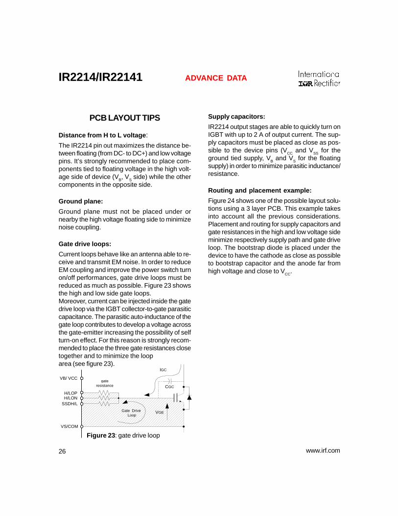
Gate drive loops:
Current loops behave like an antenna able to re-ceive and transmit EM noise. In order to reduceEM coupling and improve the power switch turnon/off performances, gate drive loops must bereduced as much as possible. Figure 23 showsthe high and low side gate loops.Moreover, current can be injected inside the gatedrive loop via the IGBT collector-to-gate parasiticcapacitance. The parasitic auto-inductance of thegate loop contributes to develop a voltage acrossthe gate-emitter increasing the possibility of selfturn-on effect. For this reason is strongly recom-mended to place the three gate resistances closetogether and to minimize the looparea (see figure 23).
gateresistance
VS/COM
VB/ VCC
H/LOPH/LON
SSDH/L
VGEGate Drive Loop
CGC
IGC
Figure 23: gate drive loop
Supply capacitors:
IR2214 output stages are able to quickly turn onIGBT with up to 2 A of output current. The sup-ply capacitors must be placed as close as pos-sible to the device pins (V
CC and V
SS for the
ground tied supply, VB and V
S for the floating
supply) in order to minimize parasitic inductance/resistance.
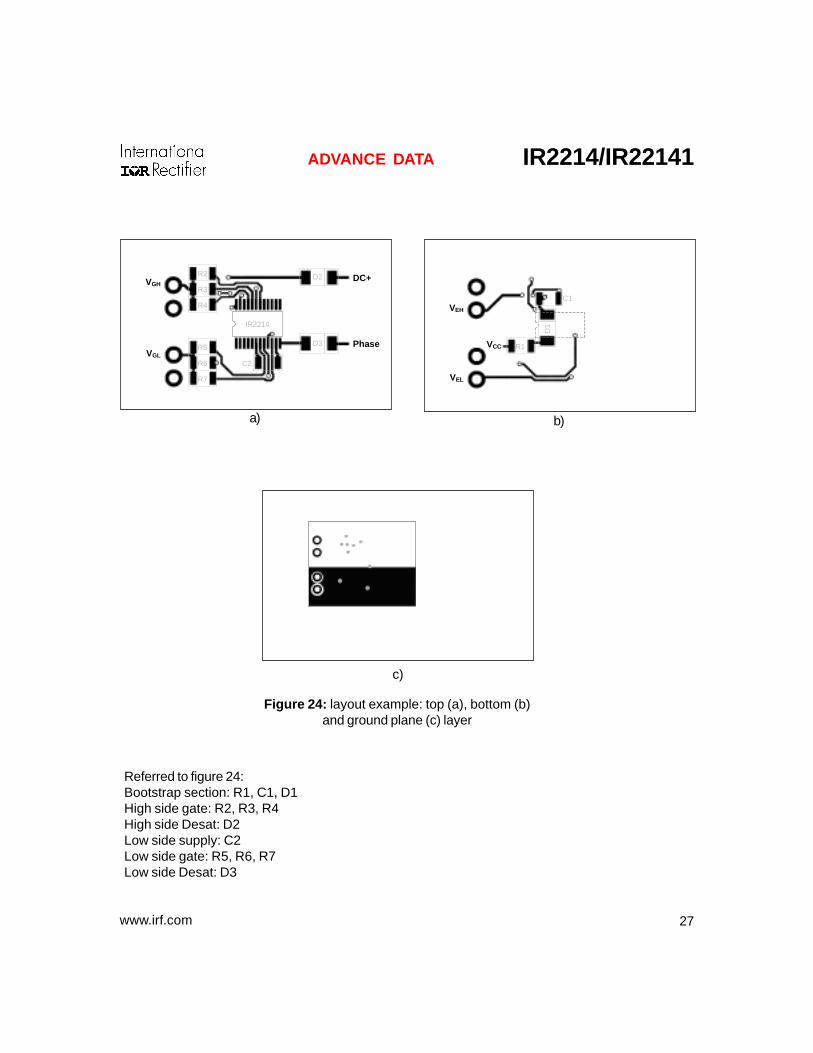
Routing and placement example:
Figure 24 shows one of the possible layout solu-tions using a 3 layer PCB. This example takesinto account all the previous considerations.Placement and routing for supply capacitors andgate resistances in the high and low voltage sideminimize respectively supply path and gate driveloop. The bootstrap diode is placed under thedevice to have the cathode as close as possibleto bootstrap capacitor and the anode far fromhigh voltage and close to V
CC.
27
IR2214/IR22141
www.irf.com
ADVANCE DATA
Referred to figure 24:Bootstrap section: R1, C1, D1High side gate: R2, R3, R4High side Desat: D2Low side supply: C2Low side gate: R5, R6, R7Low side Desat: D3
R2
R3
R4
R5
R6
R7
C2
D3
D2
IR2214
VGH
VGL
DC+
Phase
a) b)
D1
R1
C1 VEH
VEL
VCC
c)
Figure 24: layout example: top (a), bottom (b)and ground plane (c) layer
28
IR2214/IR22141
www.irf.com
ADVANCE DATA
IR WORLD HEADQUARTERS: 233 Kansas St., El Segundo, California 90245 Tel: (310) 252-7105 Data and specifications subject to change without notice. 8/6/2003
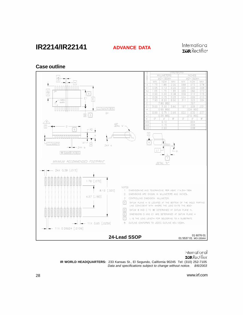
Case outline
01 6076 0101 5537 01 MO-150AH24-Lead SSOP


![Whirlpool Awe 2214 [ET]](https://img.dokumen.tips/doc/110x75/552aed114a795932118b45d7/whirlpool-awe-2214-et.jpg)


