Embed Size (px)
Citation preview

Supporting Information
Cross-linkable Fullerene Derivatives for
Solution-processed n–i-p Perovskite Solar
Cells
Konrad Wojciechowski1,†
, Ivan Ramirez1,†
, Therese Gorisse2, Olivier Dautel
3, Raghunath
Dasari4, Nobuya Sakai
1, Josue Martinez Hardigree
1, Seulki Song
5, Seth Marder
4, Moritz
Riede1, Guillaume Wantz2, Henry J. Snaith1,*
† These authors contributed equally, * [email protected]
Addresses
1. Clarendon Laboratory, University of Oxford, Parks Road, OX1 3PU, United Kingdom. 2.
IMS laboratory. Bordeaux Institute of Technology (IPB), University of Bordeaux, CNRS UMR
5218, ENSCBP, 16 Pey Berland, 33607 Pessac Cedex, France. 3. Institut Charles Gerhardt de
Montpellier, Laboratoire AM2N, UMR CNRS 5253, ENSCM 8 rue de l’Ecole Normale, 34296
Montpellier, France. 4. School of Chemistry and Biochemistry and Center for Organic Photonics and
Electronics, Georgia Institute of Technology, Atlanta, GA 30332, USA, 5. Department of Chemical
Engineering, Pohang University of Science and Technology (POSTECH), San 31, Nam-gu, Pohang,
Kyungbuk 790-784, Korea
1. Experimental section
a) Materials and device fabrication
Unless otherwise stated, all materials were purchased from Sigma-Aldrich or Alfa Aesar and used as
received. Fullerene (C60), 99.5% purity was used. Spiro-OMeTAD was purchased from Borun
Chemicals and used as received. The synthesis of the perovskite, CH3NH3PbI3-xClx has been reported
elsewhere.1

All the photovoltaic devices were fabricated on the fluorine-doped tin oxide (FTO)-coated glass
substrates, supplied by Pilkington (TEC15 of 15 Ω/sq). The FTO coating was etched with zinc powder
and 2M HCl. In order to achieve the desired pattern, areas where coating was not supposed to be
etched were covered with stripes of scotch tape. The substrates were subsequently washed with
Hellmanex solution (ca. 2 wt% in water), and then sonicated in acetone and isopropanol (IPA), 10
minutes in each solvent. Substrate preparation was completed with oxidising organic residues present
on the FTO surface by piranha etching. The substrates were immersed in the piranha etch solution
(sulphuric acid:hydrogen peroxide, 2:1 v/v), and heated at 150 °C for 2 hours. After the solution
cooled down, the samples were thoroughly rinsed with deionised water, and sonicated in acetone and
IPA. The optimised C60 compact layer was spin-coated on top of sintered FTO glass from the
solution in 1,2-dichlorobenzene (10 mg/ml) at 1500 rpm, yielding in the film thickness of
37 nm, followed by drying at 60 °C for 2 minutes. The compact layer made of crosslinkable
fulleropyrrolidine derivative containing triethoxysilane moiety (N-[3-(Triethoxysilyl)propyl]-2-
carbomethoxy-3,4-fulleropyrrolidine, sol-gel C60) was spin-coated on top of piranha-cleaned FTO
substrate from the solution in 1,2-dichlorobenzene (concentration: 2, 4 or 6 mg/ml, spinning rate: 2000
rpm). After spin-coating the film was exposed to trifluoroacetic acid vapour for 60 seconds in order to
trigger the crosslinking reaction. Then, the sample was transferred into a nitrogen-filled glovebox and
annealed at 130 °C for 30 minutes to complete the crosslinking. After that time the sample was taken
out of the glovebox and rinsed with methanol.. The electron collection layer made of the crosslinkable
PCBM derivative, PCBCB, was spin-coated on top of piranha-cleaned FTO substrate from solution in
1,2-dichlorobenzene (concentration: 5 or 10 mg/ml, spinning rate: 2000 or 3000 rpm). After spin-
coating, the sample was transferred into a nitrogen-filled glovebox and annealed at 200 °C for 10
minutes to crosslink the fullerene. Then, the sample was taken out of the glovebox and rinsed with
methanol. The synthesis of the molecule was reported by Deb et al.2 After the compact layer
deposition samples were transferred into a nitrogen-filled glovebox. Perovskite precursor solution of
the concentration of 380 mg/ml (CH3NH3I and PbCl2, 3:1 molar ratio in dimethylformamide (DMF))
was spin-coated (spinning rate: 2000 rpm) at room temperature, followed by drying at room
temperature for 30 min and annealing at 90 °C for 150 min, and 120 °C for 15 minutes, according to

the procedure reported elsewhere.3 After the perovskite annealing process finished, surface passivation
treatment was applied by spin-coating (spinning rate: 2000 rpm). a solution of iodopentafluorobenzene
(IPFB) or thiophene on top of formed perovskite, as reported previously.4,5 Subsequently, the hole
transporter was deposited by spin-coating (spinning rate: 2000 rpm) a solution of 8 wt.%
2,2’,7,7’-tetrakis-(N,N-di-pmethoxyphenylamine)9,9-spirobifluorene (spiro-OMeTAD,
purchased from Lumtec or Borun Chemical) in chlorobenzene with added tert-butylpiridine
(tBP) and lithium bis(trifluoromethanesulfonyl)imide (Li-TFSI) of 80 and 30 mol%, with
respect to spiro-OMeTAD. Finally, 50 nm thick gold electrodes were deposited on top of devices by
thermal evaporation at ~10-6 bar, through a shadow mask.
For perovskite PL measurements with different quenchers all the films were deposited on microscope
glass substrates. The perovskite layers were then sealed with a ~100nm layer of the inert polymer
poly(methylmethacrylate) (PMMA) (10 mg/ml, 1000 rpm) to reduce the impact of prolonged exposure
to moisture.
b) Characterization techniques
Atomic Force Microscopy
Surface morphology was measured in air on a vibration-isolated Asylum Instruments MFP-3D atomic
force microscope (AFM) in non-contact AC “tapping” mode in amplitude-feedback mode. Samples
were scanned using BudgetSensors Tap 150Al-G Al-coated tips (force constant of 5 N/m, resonant
frequency ~ 150 kHz). Soft-approach was used to reduce the possibility of surface-tip damage. A fast-
axis scan rate of 0.6 Hz was used to ensure topographical features were accurately retraced.
Histograms and image formatting were carried out using Gwyddion v2.45.6
Additional images were obtained using a ThermoMicroscope M5 in non-contact mode and scanning
over a range of 5 µm by 5 µm at a resolution of 256 x 256 data points. The surface roughness was
measured as the root mean-squared roughness over the scanning area.
Scanning Electron Microscopy
SEM images were obtained from a Hitachi S-4300 microscope.

Current voltage characteristics
JV characteristics of solar cells were measured under simulated AM1.5 100 mW.cm-2 sunlight (ABET
Technologies Sun 2000) with a Keithley 2400 sourcemeter. The lamp was calibrated with an NREL-
calibrated KG5 filtered silicon reference with a solar mismatch factor of 1.01. The active area of the
device was defined by a metal mask with square aperture of the area of 0.0919 cm2. The pre-masked
active area of the solar cells was approximately 0.12 cm2 nominally defined by the overlap area of the
gold and FTO electrodes. Solar cells were masked for all the current voltage measurements.
Solar cells after encapsulation, before aging test were measured under simulated AM1.5 81.1
mW.cm-2 sunlight (calibrated with Fraunhofer KG5-filtered Si-reference cell, class AAA solar
simulator).
Aging test was done at the maximum power point (MPP tracker), with a light intensity of 76.5
mW.cm-2, at the temperature of 60 °C, no active humidity control.
Photoluminescence Measurements
Time-resolved PL measurements were acquired using a time-correlated single photon counting
(TCSPC) setup (FluoTime 300, PicoQuant GmbH). Film samples were photoexcited using a 507nm
laser head (LDH-P-C-510, PicoQuant GmbH) pulsed at 1 MHz, with a pulse duration of 117 ps and
fluence of 30 nJ/cm2/pulse. The samples were exposed to the pulsed light source for ~10 minutes prior
to measurement to ensure stable sample emission. The PL was collected using a high resolution
monochromator and hybrid photomultiplier detector assembly (PMA Hybrid 40, PicoQuant GmbH).
UV-Vis absorption
UV-Vis absorption spectra were obtained using a Carry 300 Bio (Agilent Technologies) spectrometer
in transmission mode.
SCLC
Electron mobilities were extracted using the Mott-Gurney law and a field-independent mobility. To
ensure direct comparability with reported PCBCB values2, the same PEDOT/fullerene/LiF/Al
architecture was employed and Vbi taken to be 1.4 V.

2. Synthesis of sol-gel C601
Figure S1. Schematic of the sol-gel C60 synthesis.
Materials. C60 was purchased from Sigma-Aldrich (99.5%). Methyl 2,3-dibromopropionate and all
other reagents were used as purchased from Sigma-Aldrich. N-[3-(Triethoxysilyl)propyl]-2-
carbomethoxy aziridine 11 was synthesised as previously described starting from methyl 2,3-
dibromopropionate. Toluene was purchased from Sigma-Aldrich and used without further purification.
1,2-dichlorobenzene was passed through alumina column and kept over molecular sieves.
N-[3-(Triethoxysilyl)propyl]-2-carbomethoxy-3,4-fulleropyrrolidine (Sol-gel C60). 200 mg (0.14 mmol) of C60 were solubilised in 150 mL of 1,2-dichlorobenzene using an ultrasonic bath for 30
minutes. The blue solution was then degased through several vacuum-nitrogen cycles and 340 mg
(1.12 mmol) of N-[3-(triethoxysilyl)propyl]-2-carbomethoxyaziridine (1) were added. After 24 h of heating at 140 °C, the solvent was removed in vacuo. The crude product was taken back into toluene
(15 mL) and unreacted C60 separated by centrifugation. The supernatant was purified by gel
permeation chromatography using polystyrene as stationary phase (Bio-Beads SX-3) and toluene as
eluent (Figure S2). The faster eluting brown product is corresponding to the bigger and unsymmetrical
Sol-gel C60 while unreacted C60 being smaller and symmetrical remained longer on the column to elute
as the purple product. Using polystyrene gel instead of conventional silica gel allowed avoiding
premature hydrolysis of the sol-gel C60 on the silica. The collected fractions were concentrated to 20
mL and 100 mL of EtOH were added to precipitate the fullerene derivative. 106 mg (37%) of sol-gel
C60 were obtained after centrifugation. Sol-gel C60 was fully characterized by 1H,
13C and
29Si NMR
techniques. Analyses were in good accordance with the literature. 1H NMR (400 MHz, CDCl3): δδδδ
0.85-1.10 (m, 2H), 1.29 (t, 9H, J = 6.8 Hz), 1.96- 2.16 (m, 2H), 2.94-3.04 (m, 1H), 3.31-3.39 (m, 1H),
3.86 (s, 3H), 3.90 (q, 6H, J = 6.8 Hz), 4.32, (d, 1H, J = 9.2 Hz), 5.08 (d, 1H, J = 9.2 Hz), 5.10 (s, 1H). 13
C NMR (100 MHz, CDCl3): δδδδ 8.19, 18.43, 21.71, 51.50, 52.27, 55.33, 58.54, 65.21, 69.57 (Csp3,
fullerene), 72.76 (Csp3, fullerene), 77.73, 133.31, 135.44, 136.10, 136.60, 137.77, 139.73, 139.90,
140.28, 140.33, 141.85, 141.98, 142.04, 142.13, 142.16, 142.26, 142.28, 142.65, 142.68, 142.71,
143.10, 143.13, 144.48, 144.50, 144.58, 144.69, 145.30, 145.33, 145.36, 145.42, 145.44, 145.50,
145.66, 145.71, 145.81, 145.84, 146.08, 146.10, 146.25, 146.27, 146.32, 146.39, 147.34, 147.44,
151.13, 153.65, 154.75, 154.8, 170.54 (C=O). 29
Si NMR (79.5 MHz, CDCl3): δδδδ -45,35 (s, 1Si). FT-
IR: ν ν ν ν 2972 (νasCH3), 2931 (νasCH2), 2882 (νCH3), 2840 (νCH2), 1755 (νC=O), 1736 (νC=O), 1434
(νC=C, fullerene), 1175 (νasC-OSi), 1103 (νasSi-OEt), 1078 (νSi-OEt), 955 (νC-OSi) cm-1.

Figure S2. Purification of a mixture of Sol-gel C60 and unreacted C60 in toluene by gel permeation chromatography using polystyrene as stationary phase (Bio-Beads SX-3) and toluene as eluent.
The faster eluting brown product is corresponding to the bigger and unsymmetrical Sol-gel
C60 while unreacted C60 being smaller and symmetrical remained longer on the column to elute as the
purple product. Using polystyrene gel instead of conventional silica gel allowed avoiding premature
hydrolysis of the sol-gel C60 on the silica.

Figure S3. 1H NMR spectrum of Sol-gel C60 recorded at 400 MHz in CDCl3.
Figure S4. 13C NMR spectrum of Sol-gel C60 recorded at 100 MHz in CDCl3.

Figure S5. 29
Si NMR spectrum of Sol-gel C60 recorded at 79.5 MHz in CDCl3.
3. Cross-linking of the sol-gel C60
The transformation can be monitored in the sol-gel C60 FTIR spectrum (Figure S6a), from the band
intensity of the asymmetric (νasCH3) and symmetric (νsCH3) stretching vibrations of the CH3, at 2973
and 2882 cm-1, respectively. In the sol-gel C60/TFA spectrum these bands completely disappear which
is significant of the hydrolysis of the Si-OEt bonds. Similarly, formation of the Si-O-Si network can be
followed by the decrease of the band intensity of the asymmetric (νasSi-O-Et, 1103 cm-1) and
symmetric (νsSi-O-Et, 1078 cm-1
) stretching vibrations of the Si-OEt bond, the decrease of the band
intensity of the asymmetric (νasC-OSi, 1170 cm-1) and symmetric (νaC-OSi, 955 cm-1) stretching
vibrations of the CH3CH2C-OSi bond, and the appearance of the broad band from 980 to 1255 cm-1
corresponding to the asymmetric and symmetric stretching vibrations of various Si-O-Si bonds of the
silicate network. After TFA vapour exposure, absorption bands corresponding to the acid can be
observed in the sol-gel C60/TFA spectrum, with the vibration of the carbonyl (νC=O, 1784 cm-1
), C-O

(1210 cm-1), and C-F (1175 cm-1) functions. Accordingly, residual Si-OH functions (νSiO-H, around
3400 cm-1, Figure S6a) can be monitored, indicating the level of completion of the condensation
process. The removal of the TFA traces and complete condensation is achieved after 30 minutes of
thermal annealing at 130 °C in a nitrogen-filled glovebox. This is confirmed by the disappearance of
the vibrations corresponding to the TFA (νC=O, νC-O, νC-F), and the one corresponding to the
silanol (νSiO-H) in the sol-gel C60/TFA/130 °C spectrum.
a)
b)

Figure S6. (a) FT-IR spectrum of a spin-coated thin film of sol-gel C60 on a silicon wafer from a
chlorobenzene solution, before exposure to TFA vapour (black curve), after exposure to TFA vapour
(blue curve), and after exposure to TFA vapour followed by a thermal annealing at 130 °C (red curve).
The grey dashed curve is corresponding to the FT-IR spectrum of pure TFA; (b) schematic of a hybrid
network generated by the acid-catalysed hydrolysis and polycondensation of the sol-gel C60.
4. Estimation of the LUMO levels by cyclic voltammetry
The LUMO level of sol-gel C60 in solution was measured by cyclic voltammetry measurements. We
highlight that these energy levels are bound to be different to those of films, which change again upon
cross-linking. Pt wires were used as working and counter electrodes and an Ag wire as pseudo
reference electrode. The analysis were performed on a 10-3
M solution of Sol-gel C60 in an electrolyte
(0.1 M Bu4NPF6 in tetrahydrofuran solution) at room temperature with a scan rate of 100 mV/s and
ferrocenium/ferrocene (Fc+/Fc) redox couple as external reference (EFc+/Fc = 0.4 V/SCE). The cyclic
voltammogram of sol-gel C60 and PCBM (as a comparison) are shown in figure S7. The LUMO level
has been deduced from the reduction onset of the sol-gel C60 under the assumption that the energy
level of Fc is 4.7 eV below vacuum level.2
Eoxonset Fc = 0.3 V, Eredonset sol-gel C60 = - 0.55 V
ELUMO sol-gel C60 = -(4.7-(0.55+0.3)) = - 3.85 eV
Figure S7. Cyclic voltammogram of a 10-3
M solution of Sol-gel C60 in an electrolyte (0.1 M Bu4NPF6
in tetrahydrofuran solution) at room temperature with a scan rate of 100 mV/s. Ferrocene was added to
recalibrate the curves. Potential are given versus SCE.
Fc Fc+
Fc Fc+
0.3 V
- 0.55 V

5. SEM images of the fullerene-based compact layers.
Figure S8. SEM images of (a,d) sol-gel C60 after cross-linking, (b,e) PCBCB after cross-linking, and
(c,f) C60 films, processed on FTO glass.
Figure S9. AFM topography (1x1µm2) and phase images of bare FTO (a, d) , sol-gel C60 films (b, e)
before the application of solvent and after spin-coating DMF (c,f) and acquired with an Asylum
Instruments MFP-3D.
a) b) c)
d) e) f)
FTO Sol-gel C60 Sol-gel C60 + neat DMF
Height
Phase
a) b)
d)
c)
e) f)

Figure S10. Histograms corresponding to the scans presented in figure S10.
Height
Amplitude
Phase
0
Z/degree
95 65 70 75 90 85 80 100 105
0.02
0.04
60
0.06
0.08
ρ/d
egre
e-1
0.10
0.12
0.14
0.16
6. SEM images of the perovskite films processed on different fullerene layers
Figure S11. SEM images of perovskite films grown on (a) sol-gel C60, (b) PCBCB, and (c) C60 layer.
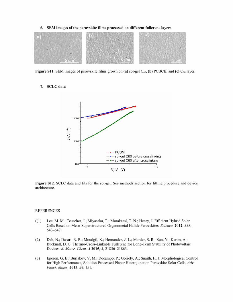
7. SCLC data
Figure S12. SCLC data and fits for the sol-gel. See methods section for fitting procedure and device
architecture.
REFERENCES
((1) Lee, M. M.; Teuscher, J.; Miyasaka, T.; Murakami, T. N.; Henry, J. Efficient Hybrid Solar
Cells Based on Meso-Superstructured Organometal Halide Perovskites. Science. 2012, 338,
643–647.
(2) Deb, N.; Dasari, R. R.; Moudgil, K.; Hernandez, J. L.; Marder, S. R.; Sun, Y.; Karim, A.;
Bucknall, D. G. Thermo-Cross-Linkable Fullerene for Long-Term Stability of Photovoltaic
Devices. J. Mater. Chem. A 2015, 3, 21856–21863.
(3) Eperon, G. E.; Burlakov, V. M.; Docampo, P.; Goriely, A.; Snaith, H. J. Morphological Control
for High Performance, Solution-Processed Planar Heterojunction Perovskite Solar Cells. Adv.
Funct. Mater. 2013, 24, 151.
a) b) c)

(4) Abate, A.; Saliba, M.; Hollman, D. J.; Stranks, S. D.; Wojciechowski, K.; Avolio, R.; Grancini,
G.; Petrozza, A.; Snaith, H. J. Supramolecular Halogen Bond Passivation of Supramolecular
Halogen Bond Passivation of Organic-Inorganic Halide Perovskite Solar Cells. Nano Lett.
2014, 14, 3247–3254.
(5) Noel, N. K.; Abate, A.; Stranks, S. D.; Parrott, E. S.; Burlakov, V. M.; Goriely, A.; Snaith, H.
J. Enhanced Photoluminescence and Solar Cell Performance via Lewis Base Passivation of
Organic-Inorganic Lead Halide Perovskites. ACS Nano 2014, 8, 9815–9821.
(6) Nečas, D.; Klapetek, P. Gwyddion: An Open-Source Software for SPM Data Analysis. Open
Phys. 2012, 10 (1).