Embed Size (px)
DESCRIPTION
Thermoelectrics
Citation preview

Heterostructured Approaches to Efficient Thermoelectric MaterialsYichi Zhang† and Galen D. Stucky*,†,‡
†Department of Chemistry and Biochemistry, University of California, Santa Barbara, California 93106-9510, United States‡Materials Department, University of California, Santa Barbara, California 93106-5050, United States
ABSTRACT: A key challenge for the materials chemist is thedevelopment of controllable and straightforward synthetic method-ologies that will integrate multiple phases/compositions with scalardesigned physical properties. The intent of this Perspective is to givea brief summary of some of the current bulk-scaled approaches thatmight help guide researchers in the design of optimal hetero-structures in large quantity for the further improvement ofthermoelectric conversion efficiency. Examples of two-phasecombinations on different length scales will be discussed with afocus on the hot carrier filtering effect that results from the selectivescattering of carriers with different energies. On the basis of thisstrategy, heterostructures fabricated by both the bottom-up solutionapproaches at low temperature and top-down solid-state depositionroutes that show promise in improving the thermoelectric figure ofmerit are highlighted.
KEYWORDS: heterostructures, thermoelectric materials, nanoinclusions, metal-semiconductor, interfacial barrier, hot carrier filtering
1. INTRODUCTION
1.1. Thermoelectric Materials. Thermoelectric (TE)materials interchange thermal energy and electricity for theutilization of waste heat and for cooling. In either case aninexpensive and scalable TE material with a high energy-conversion performance is highly desired. The upper limit ofthe TE conversion efficiency is defined by the Carnot efficiency.Figure 1a shows the energy conversion efficiency accomplishedby TE materials with different zT values across a Carnottemperature gradient, in which zT is the dimensionless figure ofmerit as defined in eq 1.
σ κ= S TzT /2 (1)
This equation allows designers to control the parameters,including Seebeck coefficient (S), electrical conductivity (σ),and thermal conductivity (κ), of materials to optimizeperformance. However, for single-phase materials, the biggestchallenge in improving the figure of merit lies in theinterdependence of each variable in eq 1. As illustrated inFigure 1b,1 the Seebeck coefficient (S) decreases as the carrierdensity increases while the other two parameters, electricalconductivity (σ) and thermal conductivity (κ), increase whenthe carrier density increases. The maximum zT fits into thedegenerate semiconductor range with an optimal carrier densityfrom 1019/cm3 to 1021/cm3.1,2 The figure of merit and thepower efficiency are therefore limited by this variableinterdependence. The consequence of this physics is that forthe single-phase thermoelectric materials that have beensynthesized and studied over the past 150 years,3,4 the TEpower efficiency has been limited to 5% or less for low-
temperature applications (<400 K) and to ∼15% or less at hightemperatures (900 K or greater).A solution to this impasse is to synthesize thermoelectric
materials that are hierarchically defined by the length scales ofthe property variables given in eq 1. However, as illustrated inFigure 1b, two pairs of variables with conflicting dependenceexist in a typical single-band electron system: electricalconductivity and thermal conductivity; and Seebeck coefficientand electrical conductivity. A successful TE material is expectedto maximize one variable without degrading the other one inthe conflicting pairs. More specifically, decoupling the electricaland thermal conductivity along with enhancement of theSeebeck coefficient while simultaneously retaining or increasingthe electrical conductivity is required. In addition to this, ascalable methodology that is able to produce the thermoelectricsystem in large quantities at low cost is necessary for practicalapplications. This is because the heat flux along a bar of lengthL is proportional to (TH − TL)/L so that the temperaturegradient across a bulk module is larger than that in a small-scaled device, resulting in a higher power efficiency asillustrated in Figure 1a.In this Perspective, the emphasis is on bulk scaled
approaches for the synthesis of heterostructures that targetthe successful simultaneous decoupling of those variables.
Special Issue: Celebrating Twenty-Five Years of Chemistry ofMaterials
Received: July 1, 2013Revised: August 19, 2013Published: September 18, 2013
Perspective
pubs.acs.org/cm
© 2013 American Chemical Society 837 dx.doi.org/10.1021/cm402150j | Chem. Mater. 2014, 26, 837−848

Ideally we wish to use a bottom-up chemistry approach togenerate property-defined phase separation of multicompo-nents on multiple length scales in order to create bulkthermoelectric systems.1.2. Single-Compositional Phase Nanostructured
Alloys. Alloyed nanostructures have been demonstrated tosuccessfully decouple the electrical and thermal conductivity byefficiently scattering phonons rather than electrons.5−12 These
alloyed nanostructures include nanocomposites made up ofnanoparticles that are prepared by either top-down5−8 orbottom-up9−12 strategies and nanoporous composites such asporous membranes13 and three-dimensional porous mono-liths.14 A substantial reduction in thermal conductivity can takeadvantage of both atomic defects in the lattice that are theresult of (1) alloyed atomic substitution along with (2) grainboundaries that are part of the hierarchical length scalenecessary to completely cover the entire phonon mean freepath (MFP) distribution range in the material system. Asshown in Figure 2, the relative reduction in thermalconductivity of silicon nanowires (Si NWs) by alloy scatteringas well as boundary scattering was quantified by Dames and
Figure 1. (a) Power generator efficiency as a function of temperaturegradient for a material with different zT values from 0.5 to 2.0. Theheat sink temperature is assumed to be 300 K. (b) Optimizing zTthrough carrier concentration tuning. Curves are based on results froma Ba8Ga16−xGe30+x sample with n = 8 × 1020 cm−3 at 600 K generatedwith a single parabolic band model. The value of 1 on the y-axiscorresponds to zT = 1; S = 400 μV/K; σ = 2 × 10⁵ S/m, and κ = 5 W/(m·K). (b) is reprinted with permission from ref 1. Copyright 2010American Chemical Society.
Figure 2. Calculated (lines) and measured (points) thermalconductivity of Si and SiGe nanowires at 300 K. Sources: [DC] =Dames and Chen;16 [Li et al.].17 The yellow area indicates the relativereduction by introducing germanium substitutions. Adapted withpermission from ref 15. Copyright 2012 Annual Reviews.
Figure 3. (a) Schematic of the of the band structure of filtering effect.Here Ec (Ev) is the conduction (valence) band edge and ΔEc (ΔEv) isthe conduction (valence) band edge difference of two materials. Eg(Eg′) is the band gap of the matrix material (second phase). Low-energy carriers are scattered more than the high-energy carriers overthe energy barrier; (b, c) Schematic of the metal−semiconductor bandalignments between n-type semiconductor and metals for Schottkycontact (b) and Ohmic contact (c). VB is the interfacial barrier withpositive (negative) sign in (b) ((c)).22
Figure 4. (a) Calculated Seebeck coefficient and conductivity for PbTeas a function of the interface potential VB; (b) the resulting powerfactor. Parameters are metallic nanoparticle diameter d = 3 nm,temperature T = 300 K, volume fraction x = 5%, and carrier density n= 2.5 × 1019 cm−3. Reprinted with permission from ref 24. Copyright2008 American Physical Society.
Chemistry of Materials Perspective
dx.doi.org/10.1021/cm402150j | Chem. Mater. 2014, 26, 837−848838

Chen.15−17 For this system, introducing defects that are of theappropriate dimensions to scatter phonons in the propertylength scale of a few nm to 1 μm is highly desirable in order tomaximize the phonon scattering and thereby reduce thethermal conductivity. However, due to the narrow phononMFP distribution in other material systems, such as telluridecompounds, using this strategy to produce an ideal hierarchicalstructure with a high degree of atomic ordering to maximizeelectron transport and appropriately dimensioned longer-rangelattice defects to maximize phonon scattering is a formidablechallenge, especially for single-phase alloy nanostructures.Therefore, the most encouraging recent breakthrough (astate-of-the-art zT value of 2.2 in a PbTe based materialsystem) in the thermoelectric field came from a hierarchicalheterostructure containing SrTe nanoinclusions instead of asingle compositional phase material.18
1.3. Multiphased Heterostructures. 1.3.1. Advantagesof Heterostructures in Theory. Taking the structure in ref 18 asone example, we define a structure containing identifiablecomposition(s) or phase(s) that is (are) integrated within themajority composition or phase and are distinguishable fromthat majority component as a heterostructure system. Thestate-of-the-art zT value of 2.2 in the PbTe-based materialsystem18 resulted from the creation of a second integratednanostructured phase with inherent different property lengthscales resulting from atomic doping and the creation of grainboundaries. This much more completely covered the phononMFP distribution range and gave a thermoelectric efficiencythat was substantially better than simpler single-phasednanostructures with related chemical compositions.18
In addition, the incorporation of multiphases provides anopportunity to produce a unique electron (carrier) transportbehavior that can be used to decouple electron transport fromthe phonon scattering at the interfaces. This is important sincethere is limited room for further reduction of thermalconductivity without losing electrical conductivity. In general,the heat transport relies on the electronic carriers as well as thelattice vibrations of the crystal, which means that the two typesof conductivities (σ and κ) are naturally coherent with eachother. This coherence can be understood quantitatively by eq 2,
in which the total thermal conductivity (κ) is split into twoparts: lattice contribution and electronic contribution. Accord-ing to the Wiedemann−Franz law, the latter contribution isrelated to electrical conductivity (σ), Lorentz number (L) andtemperature (T).
κ κ κ κ σ= + = + L TL e L (2)
This relation means that any reduction in κe will result in areduction in electrical conductivity. The desired strategy is toreduce the lattice contribution (κL) without affecting theelectronic part. However, in general, the lattice contributioncannot be reduced below the amorphous limit. One notableexception is the ultralow thermal conductivity found indisordered, layered WSe2, TE material systems.19 What ismore likely to be found is exemplified by the experimentallymeasured lattice thermal conductivity of the nanocompositemade up of ball-milled nanoparticles of p-type Bi2Te3,
5 whichapproaches the amorphous limit of Bi2Te3 as calculated usingCahill’s model.20
This result makes obvious the importance of introducingfurther improvement in thermoelectric efficiency and zT bydecoupling the variables (S and σ). Conceptually this relies onthe energy-dependent scattering of electrons (carriers) atinterfaces, which can be accomplished in heterostructures withinterfacial band offset or bending. This carrier transportbehavior, or so-called hot-carrier filtering effect in hetero-structures has been theoretically studied for several modelstructures.21−26 Specifically, superlattice structures, an integra-tion of multiple semiconductor phases, have been defined withan interfacial band offset in order to selectively scatter out thelow-energy carriers. While the low-energy carriers are beingscattered, the high-energy carriers can transport over an energybarrier as illustrated in Figure 3a.22 In contrast to the firstcategory described above that involves semiconducting phasecombinations, metal−semiconductor heterostructures definethe second group of heterostructures.23,24,26 In this group, bandbending at the metal−semiconductor contact plays animportant role in highlighting the differential transportbehaviors of the carriers with different energies.As shown in Figure 3b,c, two types of band bending can be
formed at the metal−semiconductor interfaces: (b) is the caseof a Schottky contact with positive interfacial potential while(c) shows an Ohmic contact with negative potential. Accordingto Faleev’s calculation,24 the sign of the interfacial potential(VB), positive or negative, which corresponds to the type shownin (b) or (c), does not affect either the Seebeck value or themobility. This is primarily because in this band-bendingpotential, the scattering occurs mostly as a result of thespatially slowly varying potential (band-bending), rather thanthe sharp step-like potential VB at the interface. This slowlyvarying potential is very strong for low-energy electrons, so thatthe scattering time increases with increasing energy. Thisscattering changes the total energy-dependent scattering time inthe material, thus enhancing the Seebeck coefficient. Thismechanism can be considered as a partial electron filteringeffect. The key factor is the barrier height: the absolute value ofthe potential (|VB|) must be optimized in order to maximize theenhancement in Seebeck coefficient and power factor (S2σ) asshown in Figure 4.24
In this prediction, taking the material system of a metalphase-PbTe heterostructure as an example, the optimalpotential is ∼0.1 eV.24 However, in Faleev’s calculation, ahigh volume fraction of nanoinclusions of 5% is included so
Figure 5. Room-temperature Seebeck coefficient; comparison ofexperimental and theoretical data in the in-plane direction(experimental data: squares, theory: solid curve) and cross-planedirection (experimental data: circles, theory: dashed curve for asuperlattice with conserved transverse momentum and dotted curvefor a superlattice with nonconserved transverse momentum).Experimental results indicate an improvement in the Seebeckcoefficient due to electron filtering and a maximum zT value is ∼1.5at 900 K. Reprinted with permission from ref 28. Copyright 2006American Physical Society.
Chemistry of Materials Perspective
dx.doi.org/10.1021/cm402150j | Chem. Mater. 2014, 26, 837−848839
that the nanoinclusions change the band structure of the matrixitself, which was not taken into account. This may result in aninaccurate result, as predicted by Zebarjadi et al.27 Generally,relatively large nanoparticles with a proper band bending areconsidered to be useful in partially realizing electron filtering. Inorder to simplify the interpretation of the hot carrier filteringeffect, the Mott expression eq 3 is used,
π σ
π μμ
=
= +
=
=
⎧⎨⎩⎫⎬⎭
⎧⎨⎩⎫⎬⎭
Skq
EE
kq
Tn E
n EEE
3T
d[ln( ( ))]d
3d ( )
dd ( )
d
E E
E E
2B
2
2B
2F
F (3)
In it, the Seebeck coefficient (S) depends on the energyderivative of the energy-dependent electrical conductivity σ(E)= n(E)·e(E)·μ(E) taken at the Fermi (EF) level. In thisexpression, μ(E) is the mobility, kB is the Boltzmann constant,and q is electron charge. The term, dμ(E)/dE, which is theenergy derivative of the carrier mobility in the Mott expression,can be enhanced if an appropriate barrier exists. In other words,the carriers’ transport depends on their own energies.1.3.2. Thin-Film Heterostructures Fabricated by High
Vacuum Deposition. Experimentally, these theoretical pre-dictions have been observed in some heterostructures grownusing high vacuum techniques such as molecular-beam epitaxy(MBE).28 One successful demonstration is based on the MBE-grown III−V semiconductor superlattice, In0.53Ga0.47As/In0.53Ga0.28Al0.19As.
28 In this case, these two compositionswere selected because the barrier height (VB) between themwas confirmed to be 200 meV. According to the theoreticalsimulations and experimental observations, the cross-planeSeebeck value is about two to three times higher than the in-plane Seebeck coefficient as shown in Figure 5,28 which ismainly due to the hot electron filtering that occurs in the cross-plane direction rather than in the in-plane direction, since theinterfacial barriers are uniaxial in the cross-plane direction. As aresult, the zT value of this III−V superlattice is ∼1.5 at 900 K.Similarly to this demonstration, some other thin films with
heterostructures, Te nanoparticle-dispersed Bi0.5Sb1.5Te329,30
and a misfit layered compound [(PbSe)0.99]m(WSe2)n,31,32 have
been successfully fabricated by high vacuum deposition usingelemental precursors on the basis of solid state reactions.According to Kim et al.29 and Mavrokefalos et al.’s studies,32
respectively, in the first example, Te nanoparticle-dispersedBi0.5Sb1.5Te3, in which the amount of ∼15 nm diameter Tenanoparticles is increased up to 15 vol %, the Seebeck value issignificantly improved from 169 to 248 μV/K with amoderately reduced electrical conductivity, thus resulting inan enhanced zT value by more than 30% due to the hot carrierfiltering effect as predicted by Faleev and Leonard’scalculation.24 In a second example, the in-plane thermalconductivity is measured to be three times lower in misfit-layered [(PbSe)0.99]m(WSe2)n superlattice thin films than indisordered-layered WSe2 because of interface scattering.1.3.3. Drawbacks and Challenges in Heterostructure
Fabrication. While it is valuable to investigate the physicalproperties of the atomically defined, highly crystallized thinfilms that are fabricated as heterostructures by high vacuumdeposition procedures, up-scaled syntheses of materials withdesigned structures are highly desirable, especially for thermo-electric applications. We will outline a variety of hetero-structures synthesized by either mechanical mixing techniques
or solution based chemical syntheses. In contrast to the thinfilm heterostructures for which the physics and thermoelectricproperties have been extensively studied, the synthesis andmodeling of bulk, polycrystallized, and multilength scaledmaterial systems are formidable. Impurities and interfacialboundaries induced by bulk-scaled synthetic routes are for themost part inevitable. The key challenge for the materialschemist is the development of controllable and straightforwardsynthetic methodologies that will integrate multiple phases withscalar designed physical properties. The intent of thisPerspective is to give a brief summary of some of the currentbulk scaled approaches that might help guide researchers todesign optimal heterostructures for further improvement ofthermoelectric conversion efficiency.
2. BULK SCALED APPROACHES TOINHOMOGENEOUS HETEROSTRUCTURES
In the development of heterostructures with enhancedthermoelectric performance, the use of inhomogeneous
precursor nanophase mixtures in the early synthesis stages isa valuable approach because of its simplicity. This strategy hasbeen applied to a variety of material systems including telluride,half-Heusler, and skutterudite.33−36 For example, Zhang et al.and Sumithra et al. reported a simple methodology to obtainmicronano-heterostructures by mixing the metallic nano-particles (Ni2Te and Bi) and semiconducting micrometerscaled particles as shown in Figure 6a.33,34 In addition, for the
Figure 6. (a) Cross-sectional microscopic image of Ni2Te dopedBi2Te3 heterostructures. The labels indicate the inhomogeneousdispersion of stoichiometric Bi2Te3 and Ni doped inclusions. (b)Transmission microscopic image of the inhomogeneous composite ofhalf-Heusler (hH) and full-Heusler (fH). (c, d) Low (c) and high (d)magnification image of the nanocomposite with x = 0.04 showing fHnanoparticles with broad size distribution (10−60 nm) coherentlyembedded inside the hH (Ti0.1Zr0.9NiSn) matrix. No noticeable strainis observed at the interface between the particle and the matrix,suggesting endotaxial insertion with minimal lattice distortion of thefH particle within the hH matrix. Parts a, c, and d reprinted withpermission from refs 33 and 41. Copyright 2010, 2013 AmericanChemical Society. Part b reproduced with permission from ref 35.Copyright 2013 PCCP Owner Societies.
Chemistry of Materials Perspective
dx.doi.org/10.1021/cm402150j | Chem. Mater. 2014, 26, 837−848840

half-Heusler material system, Birkel et al. used a solid-statereaction to form full-Heusler compounds in a half-Heuslermatrix by adding small amount of excess Ni to the startingreactants as shown in Figure 6b.35
One of the common characteristics in these three reportedheterostructures is the use of inhomogeneous metallic micro-structures, which limits the extent of metal−semiconductorinterfaces. In addition, a change in the charge carrier densitiesresulting from the impurities suppresses an improvement of thepower factors. Therefore, in contrast to the prediction of Faleevet al.’s model,24 the power factors of these inhomogeneousheterostructures do not exhibit a significant improvement.However, compared to the metallic inclusion-free semi-conductor, these heterostructures possess somewhat lowerthermal conductivities, mainly due to the irregular micro-structure induced phonon scattering. According to a systematicstudy by Zhao et al. on the length scale of grains,37 this extentof reduction in lattice thermal conductivity using metallicinclusions incorporated to make the heterostructure is similarto that for the single phase semiconductors made withapproximately the same amount of nanoscaled particles. Thismeans that from a synthetic perspective increasing the powerfactor is more difficult to accomplish than reducing the thermalconductivity. The inhomogeneous heterostructures made bystraightforward routes in general are not able to create thedesired interfacial barriers and/or band bending that isnecessary to selectively scatter the carriers as predicted by
theoretical models, but are able to scatter the long-wavelengthphonons as a result of the existence of their irregularmicrostructure characteristics. However, it is important tonote that this extent of reduction is not great (∼20−30%), evenwith a relatively large number of nanoscaled/micrometer-sizedinclusions, which suggests that the inhomogeneously dispersedmicrostructures are not as efficient as homogeneous nanostruc-tures in terms of phonon scattering. It is clear that the furtherdevelopment of synthetic methodologies that give a homoge-neous dispersion of the minor phase into the bulk matrix of aheterostructure is highly desirable, as discussed in Section 3below.
3. BULK SCALED APPROACHES TO HOMOGENEOUSHETEROSTRUCTURES
Both solid-state syntheses and solution based chemistrystrategies have been reported for homogeneous heterostruc-tures.38−53 Solid-state syntheses usually produce materialsystems with higher zT values than does solution basedchemistry, mainly because a high temperature process abovethe melting point can be used to minimize or better defineimpurity composition and distribution.54 However, this processis limited to phase combinations that are thermodynamicallyfavored at high temperature. Moreover, the dispersion of thenanometer scaled domains requires careful control of the phaseimmiscibility which is not universal for all the phasecombinations that are of interest. For example, for the
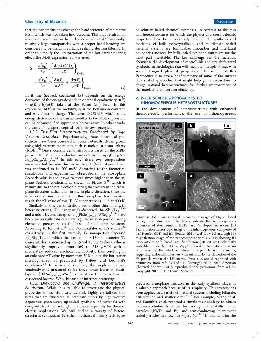
Figure 7. Microscopic images of the heterostructures: (a, b) 8% PbS-PbTe; (c, d) 3% SrS-PbS; (e, f) 3% CdS-PbS; (g, h) 2% SrTe-PbTe; (i, j) 1%CdTe-PbTe; (k) 4.1% Ag2Te-PbTe; (l) 5.5% Ag2Te-PbTe. Here, “A-B” represents “A” inclusions embedded in “B” matrix. Specifically, (a) is theEDS line scans that reveal the darker PbS particles that show increased counts for S and decreased Te. The inset in (c) is the high-resolution TEMimage of one grain boundary and that in (d) is the corresponding diffraction pattern along [011] direction that shows all spots from PbS matrix. Theinset in (e) is the STEM image that shows high number density nanostructures and that in (f) is the corresponding diffraction pattern along the[011] direction. The inset in (g) is the corresponding diffraction pattern, which confirms the crystallographic alignment of SrTe and PbTe lattices.Reproduced with permission from refs 44−49. Copyright 2010, 2012 American Chemical Society, 2011 Nature Publishing Group, and 2011 Wiley-VCH Verlag.
Chemistry of Materials Perspective
dx.doi.org/10.1021/cm402150j | Chem. Mater. 2014, 26, 837−848841

preparation of a metallic full-Heusler minor phase in a half-Heusler semiconductor major phase, as for TiNi1+xSn, themicrowave synthesis plus spark plasma sintering proceduresreported by Birkel et al. results in an inhomogeneous dispersionof the metallic full-Heusler compound in the semiconductinghalf-Heusler matrix.35 In contrast, for (Zr,Ti)Ni1+xSn, made byconventional melting plus hot pressing procedures, the metallicfull-Heusler inclusions are more homogeneous at the nanoscaleas shown in Figure 6c,d.41 These contradictory observationsdrawn from two similar material systems show, notunexpectedly, that the processing conditions can greatly modifythe resulting heterostructure properties. In this review, the twomain methodologies, solid-state reaction and solution basedroutes, are discussed further in Sections 3.1 and 3.2,respectively.3.1. Solid-State Syntheses of Homogeneous Hetero-
structures. Although bulk scaled homogeneous heterostruc-tures produced by solid-state syntheses have similar structures,because of the differences in the intrinsic properties and bandstructures of the minor phase and major matrix, no unanimousconclusion on the effects of those nanoinclusions can be drawnexcept for the reduction in lattice thermal conductivity.41−49
Figure 7 summarizes the structures currently reported includingPbS,44 SrS,45 CdS,46 SrTe,47 CdTe,48 and Ag2Te
49 in the PbTeor PbS matrix. Particularly in the cases of SrS−PbS45 andSrTe−PbTe,47 the strain maps in Figure 8 show considerableelastic strain at and around all nanoscaled precipitates. This ismainly due to the formation of coherent or semicoherentboundaries at the nanoscale (<10 nm).According to the work done by He et al., these nanoscaled
structures with the correlated dislocations and the resultantstrains have been confirmed to produce materials with moreefficient reductions in thermal conductivity at high temper-ature.50 With respect to improving the electronic properties,
especially the Seebeck coefficient, no dramatic improvementhas been reported, for several possible reasons: (1) the bandoffsets between two semiconducting phases (PbS and CdS orZnS) are rather small (<0.13 eV at 0 K) and accordingly playonly a minor role in producing hot carrier filtering;44,46 (2) theinclusions are strong dopants, which compensate for theintrinsic carriers, resulting in an extraordinarily large change incarrier density. For example, Cu-based inclusions in p-Bi2Te3switch the conductivity type from p to n as the moleconcentration of Cu goes from 0% to 5%.43 However, thereare still a few interesting observations about the Seebeckcoefficient enhancement without losing the electrical con-ductivity. For example, in the layered oxide system(Ca3Co4O9+δ)
42 and the half-Heusler system,41 the metallicinclusions are shown to increase the Seebeck coefficientsignificantly as a result of the hot carrier filtering effect dueto the appropriate band alignment among multiple phases(Figure 9).
3.2. Solution-Grown Heterostructures. The preparationof heterostructures with second phase inclusions introduced bysolid-state syntheses usually parallels the top-down synthesisstrategy. In contrast, the bottom-up approaches aim to createthe products from molecular precursors via a low-temperaturechemical reaction. Some of the nanostructures grown areshown in Figure 10.51−53 For example, Yin and co-workersproduced Bi2Te3−Te heterogeneous nanostructures that arecomposed of Bi2Te3 nanoplates and Te nanorods with variousmorphologies (“nails”, “barbells”, “syringes”, and “accordions”)by controlling the reduction kinetics of TeO3
2− and Bi3+,respectively.51 However, according to the studies done byRamanath and co-workers,52 p-type Te in n-type Bi2Te3 is notideal for thermoelectric application since both types of carrierswill cancel the thermoelectric effect to produce a lower Seebeckcoefficient. Instead, p-Sb2Te3 and Te phase combinations mayincrease the Seebeck value significantly, by two- to threefold.Although encouraging in terms of Seebeck enhancement, the
overall zT values of solution-synthesized nanostructures havebeen rarely reported, and more effort on this aspect is needed.Especially noteworthy is the example of PbTe−PbS hetero-structures made by the solution syntheses53 analogous to thestructures made by solid-state syntheses in ref 44 as discussedabove. As shown in Figure 11a, the heterostructured compositeis built on the building blocks of core−shell nanoparticles. Bycontrolling the relative dimensions between the core and theshell, the concentration of the inclusions can be tuned. Figure11b confirms the well-defined core−shell structure of thenanoparticles. After annealing, this composite with twosemiconducting phases (PbS and PbTe) exhibits a reductionin thermal conductivity comparable to that in ref 44 andthereby has a high zT of over 1.0 at ∼700 K, which is slightlylower (∼20%) than the zT record for the same compositionsmade by solid-state syntheses. This result shows considerablepromise for the use of solution syntheses to generate high zTvalues and thus avoid high temperature processes. This offersopportunities both for thermoelectric design and for thereduction of bulk fabrication costs.The three examples discussed above summarize the current
state-of-the-art for solution-grown heterostructures. From theperspective of energy-conversion efficiency, all the reports todate offer opportunities for significant improvement in thefuture. However, these examples give alternatives for theassembly of phase combinations and nanostructures that aredifficult to produce by ordinary solid-state synthesis techniques.
Figure 8. (a−c), high magnification TEM image (a) and εxx (b), εyy(c) strain maps of the image (a) of Pb0.975Na0.025S with 3% SrS sample.(d, e) high magnification TEM image (d) and shear strain distributionmap of the image (d) of 2% SrTe in PbTe. Reproduced withpermission from refs 45 and 47. Copyright 2012 American ChemicalSociety and 2011 Nature Publishing Group.
Chemistry of Materials Perspective
dx.doi.org/10.1021/cm402150j | Chem. Mater. 2014, 26, 837−848842

3.3. Solution-Based Assembly of Heterostructures.Unlike the materials discussed in Section 3.2, in this category,solution-based chemistry is used to assemble multiple phasestogether homogeneously to form a heterostructured system.This idea was first inspired by the pioneering work done byMurray and co-workers in 2004.55 In their early studies, twotypes of nanocrystals, PbTe and Ag2Te, were assembledtogether by controlling the surface chemistry. The drawbackof this route is low electronic mobility, which limits itsapplication for thermoelectric applications. Also in 2004,hydrazine-based zintl ion chemistry was reported by Mitzi etal.,56 and this has since played an important role in thedevelopment of bulk scaled approaches for the synthesis ofconducting materials. In the first example of [Sn2S6]
4−,56 theSnS2 compound plus excess sulfur was shown to be soluble inpure hydrazine to form a clear solution. One of the mostimportant features of this precursor is the ease of conversionfrom solution phase to solid state, conducting phase via solventevaporation and annealing.Besides [Sn2S6]
4−, other metal chalcogenide compoundssuch as ZnTe,57 GeSbSe,58 CuS,59 and CuInSe60 have beendeveloped using a similar strategy. In 2009, these molecularmetal chalcogenides (MMC), for example, [Sn2S6]
4−, weredemonstrated to successfully exchange with the organic cappingligand used in the synthesis of the metal nanoparticles.61 Afterthe exchange, the metal nanoparticles are suspended in thehydrophilic phase (hydrazinium precursor) while the organicsurfactants are left in the hydrophobic layer (organic nonpolar
solvent). After spin-coating the exchanged metal nanoparticleson the substrate, the nanoparticles assemble together with an“inorganic” capping ligand. After annealing, the “inorganic”capping ligand crystallizes to form an inorganic solid-stateinterlayer to facilitate in-plane electron transport as shown inFigure 12.On the basis of these studies, the Stucky and Murray groups
have recently reported heterostructured bulk-scale thick films ofAg@Sb2Te3−Te
62 and [email protected] In their reports, the
hydrazinium precursor that comprises antimony telluride andexcess tellurium is used to exchange the organic surfactants thatcap the Ag or Pt nanoparticles and thereby form ahomogeneous dispersion of metallic nanophases. After solventevaporation and annealing, the molecular metal chalcogenidecrystallizes to form a semiconducting matrix with Ag or Ptincorporated metallic nanoinclusions. The interfacial bandbending formed corresponds to a Schottky contact for Ag−Sb2Te3/Te and an Ohmic contact for Pt−Sb2Te3, respectively.Interestingly, the relative improvement in zT values of bothsamples is the same (see Table 1), although the preparationconditions are slightly different. It is worth noting that thecarrier densities may increase once the metallic nanoinclusionsare introduced; however, in comparison to the nanoinclusion-free semiconductor, the heterostructure exhibits a higherSeebeck coefficient at higher carrier density, which stronglysuggests a hot electron improvement of Seebeck coefficient.This is in agreement with Faleev and Leonard’s prediction;24
Figure 9. (a) Pisarenko plot of Ti0.1Zr0.9Ni1+xSn nanocomposites, which shows large enhancements of the thermopower (S) due to simultaneousdecrease in carrier concentration and increase in the carrier effective mass (m*) with increasing excess Ni. (b) Temperature-dependentthermoelectric figure of merit (zT) of hH(1 − x)/fH(x) bulk nanocomposites (x = 0, 0.02, 0.04, and 0.1). (c) Proposed mechanism of the filtering oflow energy electrons (from CB of hH) at the potential barrier, ΔE (reducing effective carrier density), and spatial separation of high-energy electrons(within CB of fH) from ionized impurities at nanometer scale hH/fH heterojunctions. Cyan and orange colors represent distributions of low-energyand high-energy electrons at temperatures T1 and T2 (T2 > T1) within the CB of the HH matrix. (d, e) Temperature dependence of (d) Seebeckcoefficient (S) and (e) dimensionless figure of merit for Ca3−x−yAgxLuyCo4O9+δ with x, y = 0, x = 0.05, y = 0.15, and x = 0.15, y = 0.05. Reprintedwith permission from refs 41 and 42. Copyright 2013 American Chemical Society and 2011 Wiley-VCH Verlag.
Chemistry of Materials Perspective
dx.doi.org/10.1021/cm402150j | Chem. Mater. 2014, 26, 837−848843

both types of band bending (Figure 3b,c) are able tosignificantly improve the Seebeck coefficient.In contrast to the high work-function noble metal inclusions
like Pt, in the study of Ag-based inclusions, researchers foundthat the high solubility of Ag in Te limited the annealing andoperating temperature.62 Because Ag@Sb2Te3 is less thermallystable than Pt@Sb2Te3, a metal oxide coating of the metallic Agnanoparticles is necessary in order to reduce the diffusion of Aginto the surrounding semiconducting telluride media. Recently,the Stucky group developed a route to grow a thin layer ofoxide (∼3 nm) to protect the Ag nanoparticles by atomic layer
deposition (ALD).64 The enhancement of the Seebeckcoefficient is predicted by a computer simulation by Shakouri,Stucky, and co-workers that includes an extensive ionizedimpurity scattering mechanism as well as a cutoff potential of0.2 eV for hot carrier filtering.64
This is the first demonstration of hot electron filtering withboth experimental and theoretical evidence for solutionprocessed thermoelectric heterostructures. The enhancementof thermoelectric Seebeck and conductivity results in animprovement of the zT value by a factor of 2 to ∼1.0 at 460K. This is an exceptionally high value compared to other single-phase semiconductors processed in solution with similarcomposition and carrier density.
4. OTHER HYBRID HETEROSTRUCTURES4.1. Carbon Nanotube (CNT)-Based Hybrid Structures.
Recently, studies of the thermoelectric properties of carbon-based nanomaterials such as carbon nanotubes (CNTs) andgraphenes have attracted more and more attention. Kim andco-workers investigated the thermoelectric power of individualsingle-walled carbon nanotubes (SWNTs) and discovered thatthe measured thermoelectric power correlated well with theelectrical conductance across the SWNT according to the Mottformula, eq 3.65 However, due to the metallic nature of theSWNTs with the expected inherently high thermal conductivityand low Seebeck coefficient, the composite made solely byCNTs does not provide a respectable thermoelectricefficiency.66−68 Consequently, extensive effort in this field hasfocused on hybrid composites in which the CNTs act asadditives. These hybrid structures include structural polymerCNTs,69−77 conductive polymer CNTs,78−81 metal decoratedCNTs,82−84 and solid-state compound CNTs.85−87 The mainfunction of CNTs in the polymer is to facilitate the electron
Figure 10. TEM images of the Bi2Te3−Te heterostructures. (a−c)Products prepared by Wang et al.51 using different amounts of dilutedhydrazine (2 M) in the presence of 15 μL of FeCl3/EG stock solution:(a) 130, (b) 140, and (c) 150 μL. The insets in (b) are SEM images ofa broken barbell structure. The scale bars in the insets are 100 nm. (d)Product prepared by Mehta et al.52 using microwave synthesis undertri-n-octylphosphine (TOP) protection. The inset is the corresponding[0001] zone diffraction pattern exhibiting Bragg reflections fromBi2Te3 (hexagonal spot pattern) and Te (red circles). Reprinted withpermission from refs 51 and 52. Copyright 2010 American ChemicalSociety.
Figure 11. (a) Steps for the production of nanocomposites from thebottom-up assembly of core−shell nanoparticles with different shellthicknesses. (b, c) TEM images of (PbTe)0.28@(PbS)0.72 core−shellnanoparticles with crystalline PbS shells. (d, e) TEM images of(PbTe)0.25@(PbS)0.75 core−shell nanoparticles having amorphous PbSshells. Insets display the histogram of the particle size distribution.Adapted with permission from ref 53. Copyright 2013 AmericanChemical Society.
Figure 12. (a) TEM image of an array of ∼5-nm Au NCs capped withdodecanethiol. (b) TEM image of a layer of ∼5-nm Au NCs cappedwith (N2H5)4Sn2S6. (c) TEM image of a three-dimensional super-lattice of ∼5-nm Au nanocrystals capped with (N2H5)4Sn2S6. (d)Current−voltage (I−V) scans for a film of dodecanethiol-capped 5-nmAu nanocrystals (open circles) and for a film of the same Au NCscapped with (N2H5)4Sn2S6 (black squares). Dashed arrows show thevoltage scan direction. (e) Plot of drain current ID versus drain−source voltage VDS for a nanocrystal FET with a channel composed of4.5-nm CdSe nanocrystals capped with (N2H5)4Sn2S6 and annealed at200 °C (channel length 10 mm, width 3800 mm, 110-nm-thick SiO2gate dielectric). From ref 61. Reprinted with permission from AAAS.
Chemistry of Materials Perspective
dx.doi.org/10.1021/cm402150j | Chem. Mater. 2014, 26, 837−848844

transport by creating electron transport pathways and retain thelow thermal conductivity as illustrated in Figure 13.Substantial progress in understanding and predictively
designing the properties of carbon nanotube (CNT)-basedhybrid structures is being made. For example, a zT value of 1.2has been reported for a hybrid system made using a solid-statesemiconductor and CNTs. As demonstrated by Zhang and co-workers, a ∼20% relative improvement in zT is obtained forhybrid Bi2Te3−CNTs over the CNT-free sample.87 However,the mechanism of this synergistic effect has yet to be resolved.This can be contrasted with the power factor of 160 μW/(m·K2) that is achieved for the carbon based composite made up ofSWNTs , po l y(3 ,4 - e thy l ened ioxy th iophene) :po l y -(styrenesulfonate) (PEDOT:PSS) and polyvinyl acetate
(PVAc).81 The overall zT values reported (10−3 to 10−2) forthis organic material are approximately 2 orders of magnitudelower than those observed for typical solid-state semi-conductors.
4.2. Conductive Polymer Based Organic−InorganicHybrid Structures. The use of conductive polymers forthermoelectric application was inspired by the thermoelectricmeasurement of single molecules such as thiol- and isocyanide-terminated aromatic molecules.88 An important breakthroughin this field was reported by Crispin and co-workers,89 in whichthe zT of poly(3,4-ethylenedioxythiophene) (PEDOT) ap-proached 0.25 at room temperature by controlling theoxidation level of PEDOT.As for CNTs, it is possible to combine the relatively efficient
conductive polymers with inorganic semiconductors to form ahybrid inorganic−organic system such as Te-PEDOT:PSS90
and poly(3-hexylthiophene) (P3HT)-Bi2Te3.91 In the former
example, the zT value is ∼0.1, more than 2 orders of magnitudehigher than bare Te and PEDOT:PSS, as a result of the greatlyhigher conductivity and the respectable Seebeck coefficientshown in Table 2. For the latter system, the authors depictedthe possible band alignment between p-type Bi2Te3 and organicP3HT. One advantage of incorporating the organic phase is theease of band tuning by changing the doping level. For example,in the 24 wt % doped P3HT system, the band gap of P3HT is0.2 eV, which forms a potential barrier at the P3HT−Bi2Te3interface below 0.1 eV, and therefore selectively scatters low-energy carriers rather than high-energy carriers. As aconsequence, the Seebeck coefficient of the hybrid is 118μV/K, almost five times higher than that of the bare P3HT (24μV/K).91 In summary, although these hybrid systems do notexhibit zT values as high as inorganic solid-state hetero-structures, great progress is being made. It is expected that thehighly accessible tunability of each of the components willfacilitate maximization of the overall power efficiency and zT.
5. SUMMARY AND OUTLOOKAs illustrated in Figure 14, heterostructures have proven to bean enabling route to the improvement of zT in comparisonwith the zT values for single-phase nanostructures. In Figure14, different heterostructures are categorized into severalgroups based on their base semiconductors (polymers,Bi2Te3, lead chalcogenide, and oxide). Generally, theheterostructures prepared by solid-state syntheses (column)
Table 1. Thermoelectric Properties at Room Temperature and Compositions of the Hetero-Structures and the Control Samplesin Refs 62 and 63
refnumber composition
carrier density(cm−3) mobility (cm2·V−1·s−1)
Seebeck coefficient(μV/K) conductivity (S·cm−1) power factor (μW/(cm·K2))
62 Ag@Sb2Te3−Te 8.9 × 10¹⁹ 4.1 +135 56 1.0263 Pt@Sb2Te3 2.5 × 10¹⁹ 11 +152 27 1.0262 Sb2Te3 1.7 × 10¹⁹ 26 +114 70 0.9163 Sb2Te3 1.7 × 10¹⁹ 28 +116 73 0.96
Figure 13. (a) Schematic of CNTs suspended in an aqueous emulsion.Gray spheres and red lines represent emulsion particles and CNTs,respectively. (b) Schematic of the emulsion-based composite afterdrying. The CNTs form a three-dimensional network along thesurfaces of the spherical emulsion particles. (c), (d) SEMs of the crosssections of 5 wt % CNT in poly(vinyl acetate) (PVAc). The high-magnification SEM shown in (d) is a portion of the sample in (c)indicated by a yellow solid square. It clearly shows that CNTs(indicated by arrows) are wrapped around the emulsion particles(indicated by yellow dotted lines). The scale bars in the SEMs indicate1 μm. Reprinted with permission from ref 69. Copyright 2008American Chemical Society.
Table 2. Room Temperature Thermoelectric Properties of Te/PEDOT:PSS Nanocomposites and Control Filmsa,b
system σ (S/cm) S (μV/K) power factor (μW/(m·K2)) κ (W/(m·K)) zTmax
hybrid 19.3 (±2.3) 163 (±4) 70.9 0.22−0.30c 0.10PEDOT:PSS 1.32 (±0.12) 18.9 (±0.2) 0.05 0.24−0.29 6 × 10⁻⁵
Te nanowires 0.08 (±0.03) 408 (±69) 2.7 2d 4 × 10⁻⁴
aAdapted with permission from ref 90. Copyright 2010 American Chemical Society. bReported errors are standard deviations. cFilms prepared inidentical manner to those used for electrical measurements. dBulk value.92
Chemistry of Materials Perspective
dx.doi.org/10.1021/cm402150j | Chem. Mater. 2014, 26, 837−848845

exhibit higher zT values than those from the materials made bysolution assembly or syntheses (cubic). However, the low-temperature solution-processed heterostructures are catchingup with zT values that are over 1.0.Although the mechanisms of phonon/electron transport in a
variety of heterostructures with different compositions andmicrostructures are not identical or unambiguous, severalconclusions can be drawn based on current literature results:(1) homogeneous dispersion of a minor phase into the major-phase matrix is more efficient for both phonon scattering andhot carrier filtering than is an inhomogeneous dispersion; (2)hot carrier filtering requires an appropriate interfacial barrier orband bending to selectively scatter low-energy carriers; (3) thebarrier height must be below 0.2 eV for selective scattering andto maintain or enhance carrier mobility; (4) the combination ofmultiple phases must be thermally stable. In other words, theinsolubility of one phase into the other must remain constantover the entire temperature range of processing and operations.Chemistry synthesis techniques are a double-edged sword.
Impurity levels are inherently higher than they are for MBE orclean room synthetic procedures, so that there are moresynthetic variables to control in terms of composition,hierarchical structure, and property scaled heterostructureassembly. This larger synthesis phase space in principle canbe valuable for providing access for the enabling of complexcomposite thermoelectric materials with high power efficien-cies. We believe that to do this with bulk synthesis chemistrytechniques, high throughput screening is highly desirable. Theoptimal phase combination has to be selected from acomprehensive library of heterostructures. For example, inaddition to Ag@Sb2Te3−Te
62 and Pt@Sb2Te3,63 screening of
numerous other types and combinations of metals is needed. Inaddition, compared to the solid-state-synthesized heterostruc-tures, low-temperature processes based on hydraziniumchemistry or polymer chemistry offer some flexibility of timeand processing for the fabrication of thermoelectric devices.89
■ AUTHOR INFORMATION
NotesThe authors declare no competing financial interest.Biographies
Yichi Zhang earned his bachelor’s degree from Peking University in2008. After being awarded his Ph.D. degree from University ofCalifornia, Santa Barbara, in June 2013, he joined Dow Chemical Inc.He has published 19 scientific articles including four papers with firstauthorship. Honors include the Corning Fellowship (2010), StudentAward at the 2nd Nano Today International Conference (2011), andthe Excellence in Graduate Research Award at the 244th AmericanChemical Society Meeting (2012).
After earning his doctorate from Iowa State University in 1962, GalenStucky held positions at the University of Illinois, Sandia, and DuPontbefore joining the faculty of the University of California, Santa Barbara,in 1985. He has published over 700 scientific articles and has beenawarded 20 patents. Honors include the ACS Award in Chemistry ofMaterials (2002), the ATACCC Award (2008), and election to theNational Academy of Sciences (2013).
■ ACKNOWLEDGMENTS
The authors are grateful for support from the Center forEnergy Efficient Materials, an Energy Frontier Research Centerfunded by the U.S. Department of Energy, Office of Science,Basic Energy Sciences, under Award DE-SC0001009.
■ REFERENCES(1) Toberer, E. S.; May, A. F.; Snyder, G. J. Chem. Mater. 2010, 22,624−634.(2) Snyder, G. J.; Toberer, E. S. Nat. Mater. 2008, 7, 105−114.(3) Seebeck, T. J.; von Oettingen, A. Magnetische Polarisation derMetalle und Erze durch Temperatur-Differenz; W. Engelmann: Leipzig,1895; pp 265−373. http://catalog.hathitrust.org/api/volumes/oclc/7502427.html.(4) Peltier, J. C. Ann. Chim. 1834, 56, 371−386.(5) Poudel, B.; Hao, Q.; Ma, Y.; Lan, Y.; Minnich, A.; Yu, B.; Yan, X.;Wang, D.; Muto, A.; Vashaee, D.; Chen, X.; Liu, J.; Dresselhaus, M. S.;Chen, G.; Ren, Z. Science 2008, 320, 634−638.(6) Joshi, G.; Lee, H.; Lan, Y.; Wang, X.; Zhu, G.; Wang, D.; Gould,R. W.; Cuff, D. C.; Tang, M. Y.; Dresselhaus, M. S.; Chen, G.; Ren, Z.Nano Lett. 2008, 8, 4670−4674.(7) Yan, X.; Poudel, B.; Ma, Y.; Liu, W. S.; Joshi, G.; Wang, H.; Lan,Y.; Wang, D.; Chen, G.; Ren, Z. F. Nano Lett. 2010, 10, 3373−3378.(8) Xie, W.; He, J.; Kang, H. J.; Tang, X.; Zhu, S.; Laver, M.; Wang,S.; Copley, J. R. D.; Brown, C. M.; Zhang, Q.; Tritt, T. M. Nano Lett.2010, 10, 3283−3289.(9) Mehta, R. J.; Zhang, Y.; Karthik, C.; Singh, B.; Siegel, R. W.;Borca-Tasciuc, T.; Ramanath, G. Nat. Mater. 2012, 11, 233−40.(10) Kovalenko, M. V; Spokoyny, B.; Lee, J.; Scheele, M.; Weber, A.;Perera, S.; Landry, D.; Talapin, D. V. J. Am. Chem. Soc. 2009, 131,597−602.(11) Dirmyer, M. R.; Martin, J.; Nolas, G. S.; Sen, A.; Badding, J. V.Small 2009, 5, 933−937.(12) Scheele, M.; Oeschler, N.; Meier, K.; Kornowski, A.; Klinke, C.;Weller, H. Adv. Funct. Mater. 2009, 19, 3476−3483.(13) Tang, J.; Wang, H.-T.; Lee, D. H.; Fardy, M.; Huo, Z.; Russell,T. P.; Yang, P. Nano Lett. 2010, 10, 4279−4283.(14) Zhang, Y.; Day, T.; Snedaker, M. L.; Wang, H.; Kramer, S.;Birkel, C. S.; Ji, X.; Liu, D.; Snyder, G. J.; Stucky, G. D. Adv. Mater.2012, 24, 5065−5670.(15) Toberer, E. S.; Baranowski, L. L.; Dames, C. Annu. Rev. Mater.Res. 2012, 42, 179−209.(16) Dames, C.; Chen, G. In ThermoelectricsHandbook: Macro toNano; Rowe, D. M., Ed.; CRC Press: Boca Raton, FL; p 1014.
Figure 14. Summary of zT values of the bulk scaled heterostructuresdiscussed in this review. CNTs, Bi2Te3, PbTe, and oxide basedheterostructures are shown in blue, green, red, and purple, respectively.The cube on the yellow base indicates the corresponding syntheticroute is solution based, and the column on the blue base indicates theroute is solid-state based. The corresponding reference is labeledrespectively.
Chemistry of Materials Perspective
dx.doi.org/10.1021/cm402150j | Chem. Mater. 2014, 26, 837−848846

(17) Li, D. Y.; Wu, Y. Y.; Kim, P.; Shi, L.; Yang, P. D.; Majumdar, A.Appl. Phys. Lett. 2003, 83, 2934−2936.(18) Biswas, K.; He, J.; Blum, I. D.; Wu, C.-I.; Hogan, T. P.; Seidman,D. N.; Dravid, V. P.; Kanatzidis, M. G. Nature 2012, 489, 414−418.(19) Chiritescu, C.; Cahill, D. G.; Nguyen, N.; Johnson, D.; Bodapati,A.; Kebilinski, P.; Zschack, P. Science 2007, 315, 351−353.(20) Cahill, D. G.; Watson, S. K.; Pohl, R. O. Phys. Rev. B 1992, 46,6131−6140.(21) Popescu, A.; Woods, L.; Martin, J.; Nolas, G. Phys. Rev. B 2009,79, 205302.(22) Zhou, J.; Li, X.; Chen, G.; Yang, R. Phys. Rev. B 2010, 82,115308.(23) Moyzhes, B.; Nemchinsky, V. Appl. Phys. Lett. 1998, 73, 1895−1897.(24) Faleev, S.; Leonard, F. Phys. Rev. B 2008, 77, 214304.(25) Heremans, J.; Thrush, C.; Morelli, D. Phys. Rev. B 2004, 70,115334.(26) Vashaee, D.; Shakouri, A. Phys. Rev. Lett. 2004, 92, 106103.(27) Zebarjadi, M.; Esfarjani, K.; Shakouri, A.; Bahk, J.-H.; Bian, Z.;Zeng, G.; Bowers, J.; Lu, H.; Zide, J.; Gossard, A. Appl. Phys. Lett.2009, 94, 202105.(28) Zide, J.; Vashaee, D.; Bian, Z.; Zeng, G.; Bowers, J.; Shakouri,A.; Gossard, A. Phys. Rev. B 2006, 74, 205335.(29) Kim, S. Il; Ahn, K.; Yeon, D.-H.; Hwang, S.; Kim, H.-S.; Lee, S.M.; Lee, K. H. Appl. Phys. Express 2011, 4, 091801.(30) Kim, S. I.; Hwang, S.; Roh, J. W.; Ahn, K.; Yeon, D.-H.; Lee, K.H.; Kim, S. W. J. Mater. Res. 2012, 27, 2449−2456.(31) Lin, Q.; Smeller, M.; Heideman, C. L.; Zschack, P.; Koyano, M.;Anderson, M. D.; Kykyneshi, R.; Keszler, D. A.; Anderson, I. M.;Johnson, D. C Chem. Mater. 2010, 22, 1002−1009.(32) Mavrokefalos, A.; Lin, Q.; Beekman, M.; Seol, J. H.; Lee, Y. J.;Kong, H.; Pettes, M. T.; Johnson, D. C.; Shi, L. Appl. Phys. Lett. 2010,96, 181908.(33) Zhang, Y.; Wang, H.; Kramer, S.; Shi, Y.; Zhang, F.; Snedaker,M.; Ding, K.; Moskovits, M.; Snyder, G. J.; Stucky, G. D. ACS Nano2011, 5, 3158−3165.(34) Sumithra, S.; Takas, N. J.; Misra, D. K.; Nolting, W. M.; Poudeu,P. F. P.; Stokes, K. L. Adv. Energy Mater. 2011, 1, 1141−1147.(35) Birkel, C. S.; Douglas, J. E.; Lettiere, B. R.; Seward, G.; Verma,N.; Zhang, Y.; Pollock, T. M.; Seshadri, R.; Stucky, G. D. Phys. Chem.Chem. Phys. 2013, 15, 6990−6997.(36) Puneet, P.; He, J.; Zhu, S.; Tritt, T. M. J. Appl. Phys. 2012, 112,033710.(37) Zhao, L.-D.; Zhang, B.-P.; Liu, W.-S.; Li, J.-F. J. Appl. Phys. 2009,105, 23704−23706.(38) Hsu, K. F.; Loo, S.; Guo, F.; Chen, W.; Dyck, J. S.; Uher, C.;Hogan, T.; Polychroniadis, E. K.; Kanatzidis, M. G. Science 2004, 303,818−821.(39) Kanatzidis, M. G. Chem. Mater. 2010, 22, 648−659.(40) Poudeu, P. F. P.; Gueguen, A.; Wu, C.-I.; Hogan, T.; Kanatzidis,M. G. Chem. Mater. 2010, 22, 1046−1053.(41) Liu, Y.; Sahoo, P.; Makongo, J. P. A.; Zhou, X.; Kim, S.-J.; Chi,H.; Uher, C.; Pan, X.; Poudeu, P. F. P. J. Am. Chem. Soc. 2013, 135,7486−95.(42) Van Nong, N.; Pryds, N.; Linderoth, S.; Ohtaki, M. Adv. Mater.2011, 23, 2484−90.(43) Han, M.-K.; Ahn, K.; Kim, H.; Rhyee, J.-S.; Kim, S.-J. J. Mater.Chem. 2011, 21, 11365−11370.(44) Girard, S. N.; He, J.; Li, C.; Moses, S.; Wang, G.; Uher, C.;Dravid, V. P.; Kanatzidis, M. G. Nano Lett. 2010, 10, 2825−31.(45) Zhao, L.-D.; He, J.; Wu, C.-I.; Hogan, T. P.; Zhou, X.; Uher, C.;Dravid, V. P.; Kanatzidis, M. G. J. Am. Chem. Soc. 2012, 134, 7902−12.(46) Zhao, L.-D.; He, J.; Hao, S.; Wu, C.-I.; Hogan, T. P.; Wolverton,C.; Dravid, V. P.; Kanatzidis, M. G. J. Am. Chem. Soc. 2012, 134,16327−36.(47) Biswas, K.; He, J.; Zhang, Q.; Wang, G.; Uher, C.; Dravid, V. P.;Kanatzidis, M. G. Nat. Chem. 2011, 3, 160−6.
(48) Ahn, K.; Han, M.-K.; He, J.; Androulakis, J.; Ballikaya, S.; Uher,C.; Dravid, V. P.; Kanatzidis, M. G. J. Am. Chem. Soc. 2010, 132,5227−35.(49) Pei, Y.; Lensch-Falk, J.; Toberer, E. S.; Medlin, D. L.; Snyder, G.J. Adv. Funct. Mater. 2011, 21, 241−249.(50) He, J.; Girard, S. N.; Kanatzidis, M. G.; Dravid, V. P. Adv. Funct.Mater. 2010, 20, 764−772.(51) Wang, W.; Goebl, J.; He, L.; Aloni, S.; Hu, Y.; Zhen, L.; Yin, Y. J.Am. Chem. Soc. 2010, 132, 17316−17324.(52) Mehta, R. J.; Karthik, C.; Singh, B.; Teki, R.; Borca-Tasciuc, T.;Ramanath, G. ACS Nano 2010, 4, 5055−60.(53) Ibanez, M.; Zamani, R.; Gorsse, S.; Fan, J.; Silvia, O.; Cadavid,D.; Morante, J. R.; Arbiol, J.; Cabot, A. ACS Nano 2013, 7, 2573−2586.(54) Saramat, A.; Svensson, G.; Palmqvist, A. E. C. J. Appl. Phys.2006, 99, 023708.(55) Urban, J. J.; Talapin, D. V; Shevchenko, E. V; Kagan, C. R.;Murray, C. B. Nat. Mater. 2007, 6, 115−21.(56) Mitzi, D. B.; Kosbar, L. L.; Murray, C. E.; Copel, M.; Afzali, A.Nature 2004, 428, 299−303.(57) Mitzi, D. B. Inorg. Chem. 2005, 44, 7078−86.(58) Milliron, D. J.; Raoux, S.; Shelby, R. M.; Jordan-Sweet, J. Nat.Mater. 2007, 6, 352−6.(59) Mitzi, D. Inorg. Chem. 2007, 46, 926−931.(60) Milliron, D. J.; Mitzi, D. B.; Copel, M.; Murray, C. E. Chem.Mater. 2006, 18, 587−590.(61) Kovalenko, M. V; Scheele, M.; Talapin, D. V. Science 2009, 324,1417−20.(62) Zhang, Y.; Snedaker, M. L.; Birkel, C. S.; Mubeen, S.; Ji, X.; Shi,Y.; Liu, D.; Liu, X.; Moskovits, M.; Stucky, G. D. Nano Lett. 2012, 12,1075−1080.(63) Ko, D.-K.; Kang, Y.; Murray, C. B. Nano Lett. 2011, 11, 2841−2844.(64) Zhang, Y.; Bahk, J.-H.; Lee, J.; Birkel, C. S.; Snedaker, M. L.; Liu,D.; Zeng, H.; Moskovits, M.; Shakouri, A.; Stucky, G. D. Adv. Mater.2013, submitted.(65) Small, J.; Perez, K.; Kim, P. Phys. Rev. Lett. 2003, 91, 256801.(66) Yu, F.; Hu, L.; Zhou, H.; Qiu, C.; Yang, H.; Chen, M.; Lu, J.;Sun, L. J. Nanosci. Nanotechnol. 2013, 13, 1335−8.(67) Bradley, K.; Jhi, S.; Collins, P.; Hone, J.; Cohen, M.; Louie, S.;Zettl, A. Phys. Rev. Lett. 2000, 85, 4361−4.(68) Haskins, J.; Kinaci, A.; Sevik, C.; Sevincli, H.; Cuniberti, G.;Cagin, T. ACS Nano 2011, 5, 3779−3787.(69) Yu, C.; Kim, Y. S.; Kim, D.; Grunlan, J. C. Nano Lett. 2008, 8,4428−32.(70) Hewitt, C. A.; Kaiser, A. B.; Roth, S.; Craps, M.; Czerw, R.;Carroll, D. L. Appl. Phys. Lett. 2011, 98, 183110.(71) Choi, Y.; Kim, Y.; Park, S.-G.; Kim, Y.-G.; Sung, B. J.; Jang, S.-Y.;Kim, W. Org. Electron. 2011, 12, 2120−2125.(72) Yao, Q.; Chen, L.; Zhang, W.; Liufu, S.; Chen, X. ACS Nano2010, 4, 2445−2451.(73) Wang, Q.; Yao, Q.; Chang, J.; Chen, L. J. Mater. Chem. 2012, 22,17612−17618.(74) Zhang, K.; Davis, M.; Qiu, J.; Hope-Weeks, L.; Wang, S.Nanotechnology 2012, 23, 385701.(75) Liu, J.; Sun, J.; Gao, L. Nanoscale 2011, 3, 3616−9.(76) Freeman, D. D.; Choi, K.; Yu, C. PloS One 2012, 7, e47822.(77) Moriarty, G. P.; Wheeler, J. N.; Yu, C.; Grunlan, J. C. Carbon2012, 50, 885−895.(78) Kim, D.; Kim, Y.; Choi, K.; Grunlan, J. C.; Yu, C. ACS Nano2010, 4, 513−523.(79) Bounioux, C.; Díaz-Chao, P.; Campoy-Quiles, M.; Martín-Gonzalez, M. S.; Goni, A. R.; Yerushalmi-Rozen, R.; Muller, C. EnergyEnviron. Sci. 2013, 6, 918−925.(80) Kim, G. H.; Hwang, D. H.; Woo, S. I. Phys. Chem. Chem. Phys.2012, 14, 3530−6.(81) Yu, C.; Choi, K.; Yin, L.; Grunlan, J. C. ACS Nano 2011, 5,7885−92.
Chemistry of Materials Perspective
dx.doi.org/10.1021/cm402150j | Chem. Mater. 2014, 26, 837−848847

(82) Hewitt, C. A; Kaiser, A. B.; Roth, S.; Craps, M.; Czerw, R.;Carroll, D. L. Nano Lett. 2012, 12, 1307−10.(83) Fernandes, G. E.; Kim, J. H.; Xu, J. Mater. Res. Bull. 2013, 48,2950−2954.(84) Yu, C.; Ryu, Y.; Yin, L.; Yang, H. ACS Nano 2011, 5, 1297−1303.(85) Kim, K. T.; Choi, S. Y.; Shin, E. H.; Moon, K. S.; Koo, H. Y.;Lee, G.-G.; Ha, G. H. Carbon 2013, 52, 541−549.(86) Suh, D.; Lee, D.; Kang, C.; Shon, I.-J.; Kim, W.; Baik, S. J. Mater.Chem. 2012, 22, 21376−21381.(87) Zhang, Y.; Wang, X. L.; Yeoh, W. K.; Zheng, R. K.; Zhang, C.Appl. Phys. Lett. 2012, 101, 031909.(88) Tan, A.; Balachandran, J.; Sadat, S.; Gavini, V.; Dunietz, B. D.;Jang, S.-Y.; Reddy, P. J. Am. Chem. Soc. 2011, 133, 8838−41.(89) Bubnova, O.; Khan, Z. U.; Malti, A.; Braun, S.; Fahlman, M.;Berggren, M.; Crispin, X. Nat. Mater. 2011, 10, 429−33.(90) See, K. C.; Feser, J. P.; Chen, C. E.; Majumdar, A.; Urban, J. J.;Segalman, R. A. Nano Lett. 2010, 10, 4664−7.(91) He, M.; Ge, J.; Lin, Z.; Feng, X.; Wang, X.; Lu, H.; Yang, Y.;Qiu, F. Energy Environ. Sci. 2012, 5, 8351−8358.(92) Goncalves, P.; , A.; Lopes, E. B.; Alves, E.; Barradas, N. P.;Franco, N.; Rouleau, O.; Godart, C. New Approaches to Thermo-electric Materials. In Properties and Applications of ThermoelectricMaterials; Springer: Dordrecht, 2009; p 51.
Chemistry of Materials Perspective
dx.doi.org/10.1021/cm402150j | Chem. Mater. 2014, 26, 837−848848