Embed Size (px)
Citation preview

SVTC SolarA Photovoltaic Product Development Center
Stephen EmpedoclesDirector of Business DevelopmentSVTC Solar Division [email protected]
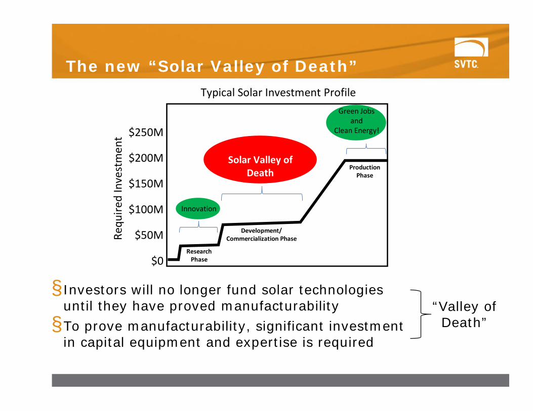
§ Investors will no longer fund solar technologies until they have proved manufacturability§ To prove manufacturability, significant investment
in capital equipment and expertise is required
“Valley of Death”
The new “Solar Valley of Death”
$250M
$200M
$150M
$100M
$50M
$0Research
Phase
Development/Commercialization Phase
Production Phase
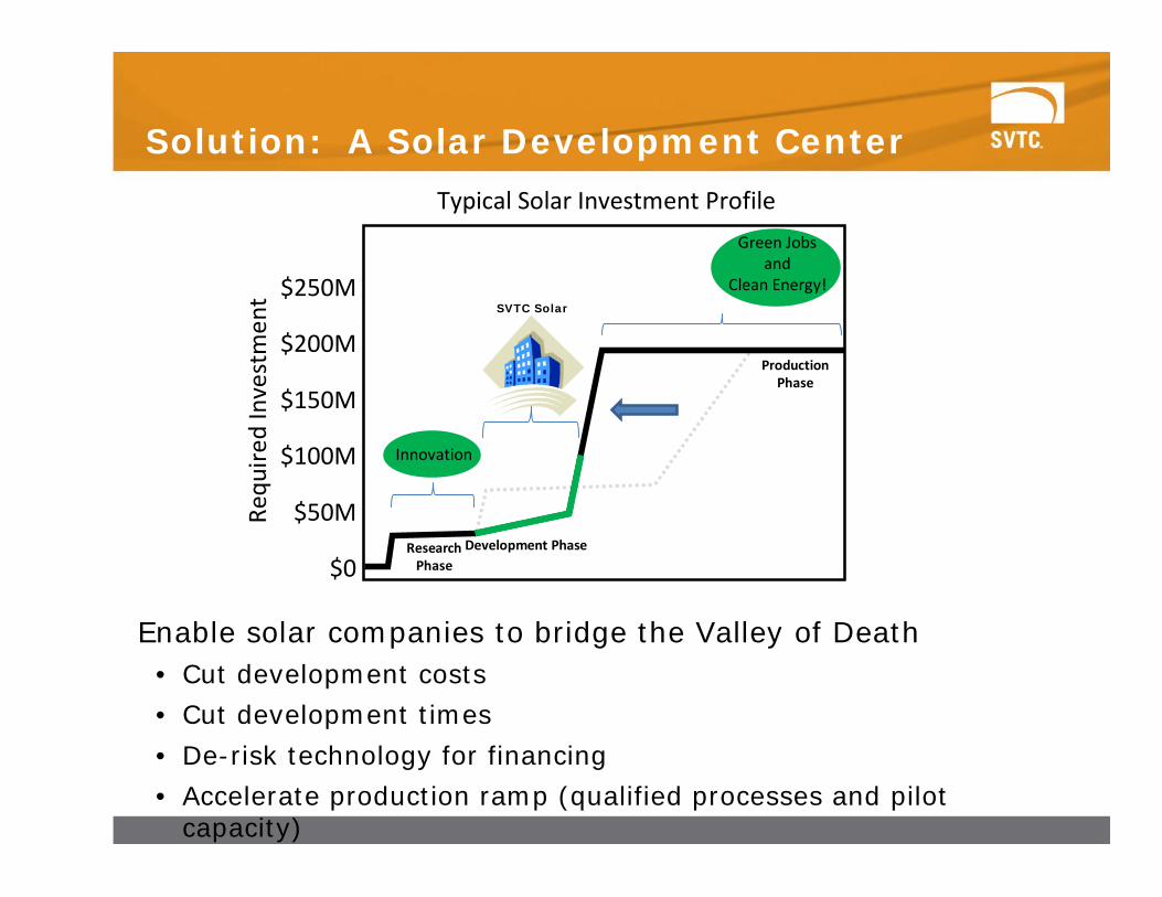
Typical Solar Investment Profile
Innovation
Green Jobs and
Clean Energy!
Solar Valley of Death
Requ
ired
Inve
stm
ent
$250M
$200M
$150M
$100M
$50M
$0Research
PhaseDevelopment Phase
Typical Solar Investment Profile
Innovation
Requ
ired
Inve
stm
ent
Solution: A Solar Development Center
SVTC Solar
Enable solar companies to bridge the Valley of Death• Cut development costs
• Cut development times
• De-risk technology for financing
• Accelerate production ramp (qualified processes and pilot capacity)
Production Phase
Green Jobs and
Clean Energy!

• Not a research center . . . . . . a product development and piloting center
• High synergy with PV research centers like NREL’s NCPV
Synergy with PV Research Centers
p.4
Basic Research
Volume Manufacturing
Pilot Production
Product Development
PV Cell Makers
• Universities• NREL NCPV• HUBS• DoE R&D Programs
SiSoC
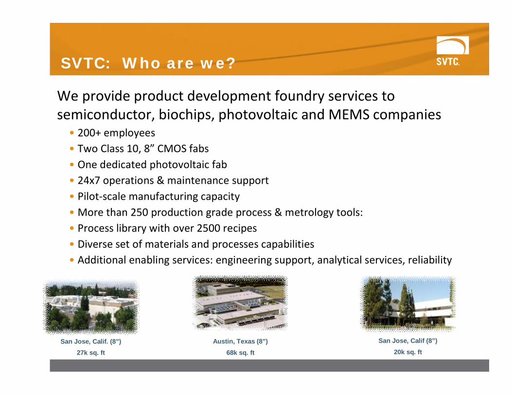
Austin, Texas (8”)
68k sq. ft
SVTC: Who are we?
San Jose, Calif. (8”)27k sq. ft
San Jose, Calif (8”)
20k sq. ft
We provide product development foundry services to semiconductor, biochips, photovoltaic and MEMS companies
• 200+ employees• Two Class 10, 8” CMOS fabs• One dedicated photovoltaic fab• 24x7 operations & maintenance support• Pilot-scale manufacturing capacity• More than 250 production grade process & metrology tools:• Process library with over 2500 recipes• Diverse set of materials and processes capabilities• Additional enabling services: engineering support, analytical services, reliability
p.6
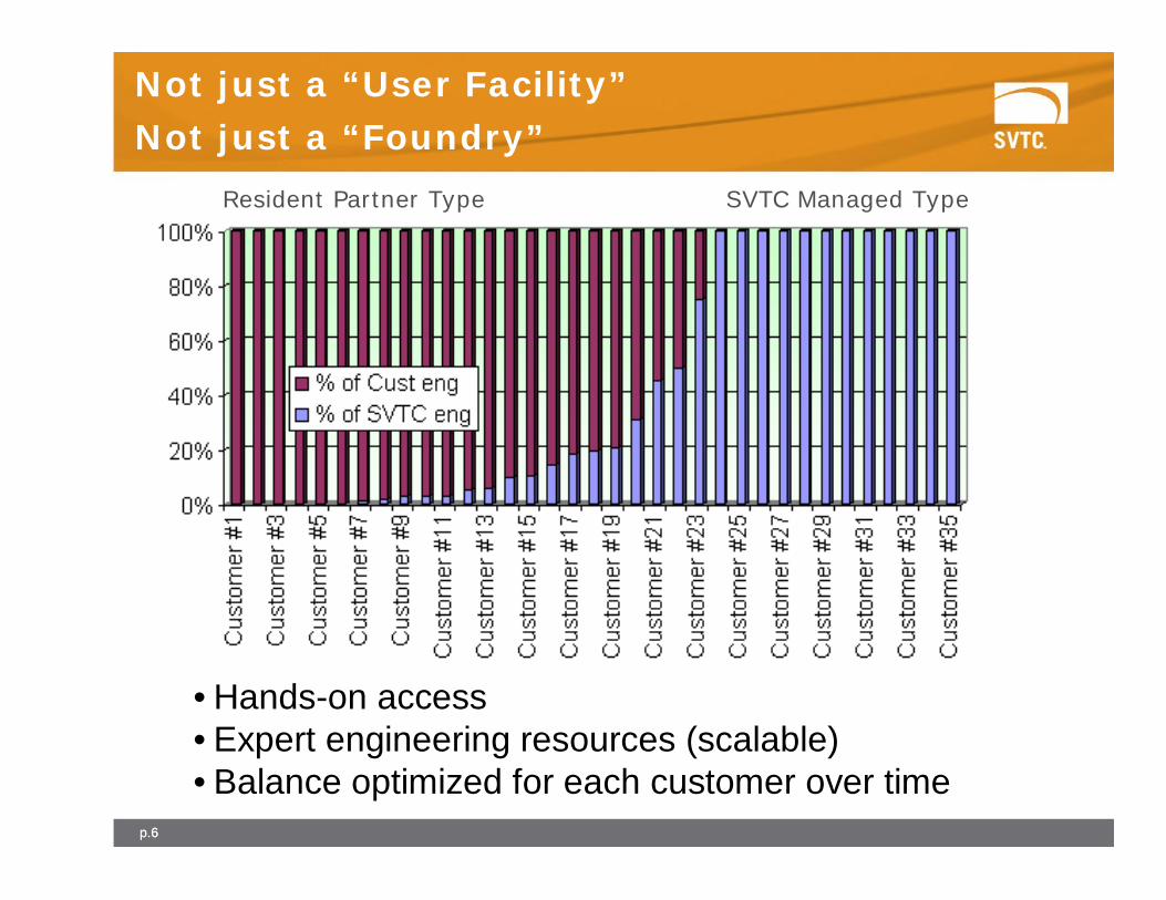
Not just a “User Facility”Not just a “Foundry”
p.6
Resident Partner Type SVTC Managed Type
• Hands-on access • Expert engineering resources (scalable)• Balance optimized for each customer over time
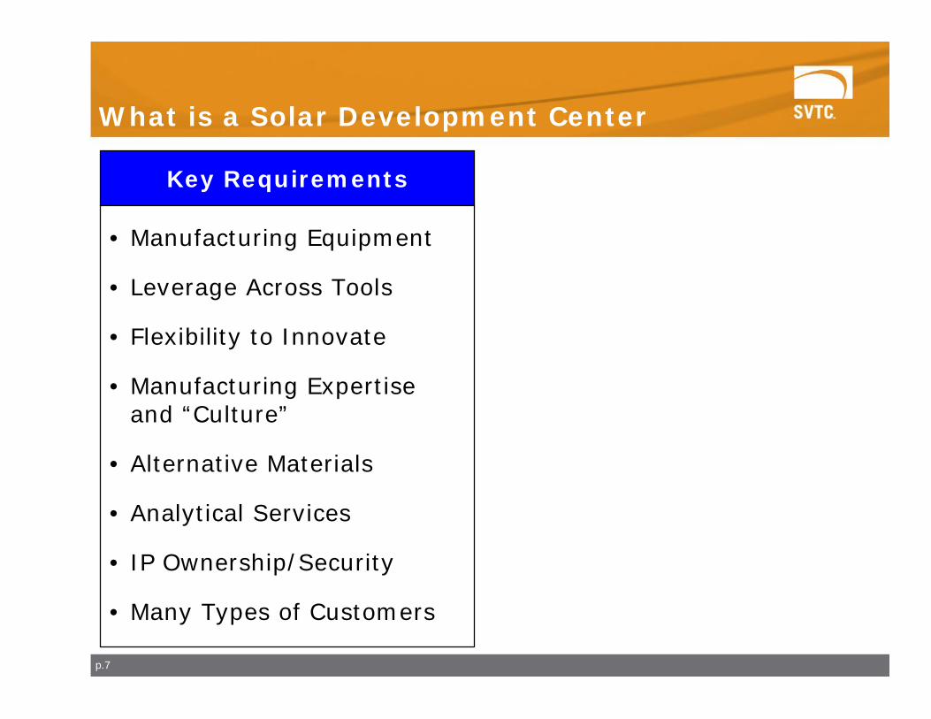
What is a Solar Development Center
p.7
• Manufacturing Equipment
• Leverage Across Tools
• Flexibility to Innovate
• Manufacturing Expertise and “Culture”
• Alternative Materials
• Analytical Services
• IP Ownership/Security
• Many Types of Customers
Key Requirements
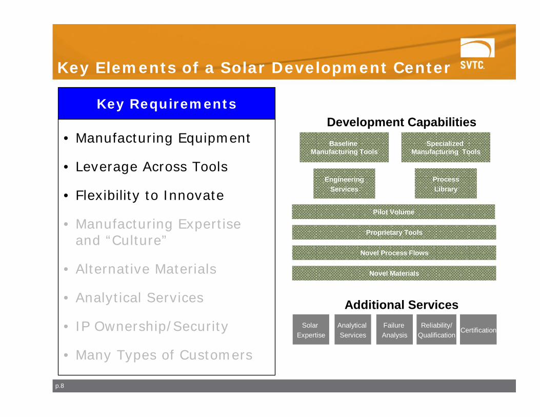
Key Elements of a Solar Development Center
p.8
Proprietary Tools
Novel Process Flows
Novel Materials
Additional ServicesSolar
ExpertiseAnalytical Services
Reliability/Qualification
CertificationFailure Analysis
Development CapabilitiesBaseline
Manufacturing Tools
EngineeringServices
ProcessLibrary
Specialized Manufacturing Tools
Pilot Volume
• Manufacturing Equipment
• Leverage Across Tools
• Flexibility to Innovate
• Manufacturing Expertise and “Culture”
• Alternative Materials
• Analytical Services
• IP Ownership/Security
• Many Types of Customers
Key Requirements
p.9
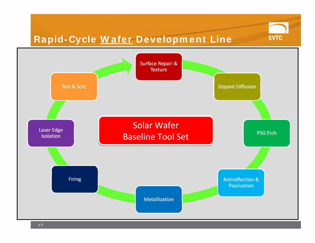
Rapid-Cycle Wafer Development Line
Solar Wafer Baseline Tool Set
Solar Wafer Baseline Tool Set
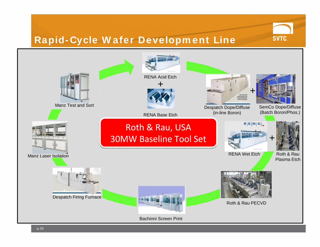
p.10
Roth & Rau, USA30MW Baseline Tool Set
Roth & Rau, USA30MW Baseline Tool Set
Bachinni Screen Print
Despatch Firing Furnace
Manz Laser Isolation
Manz Test and Sort SemCo Dope/Diffuse (Batch Boron/Phos.)
+Despatch Dope/Diffuse
(in-line Boron)
Roth & Rau PECVD
RENA Base Etch
RENA Acid Etch
+
RENA Wet Etch Roth & RauPlasma Etch
+
Rapid-Cycle Wafer Development Line
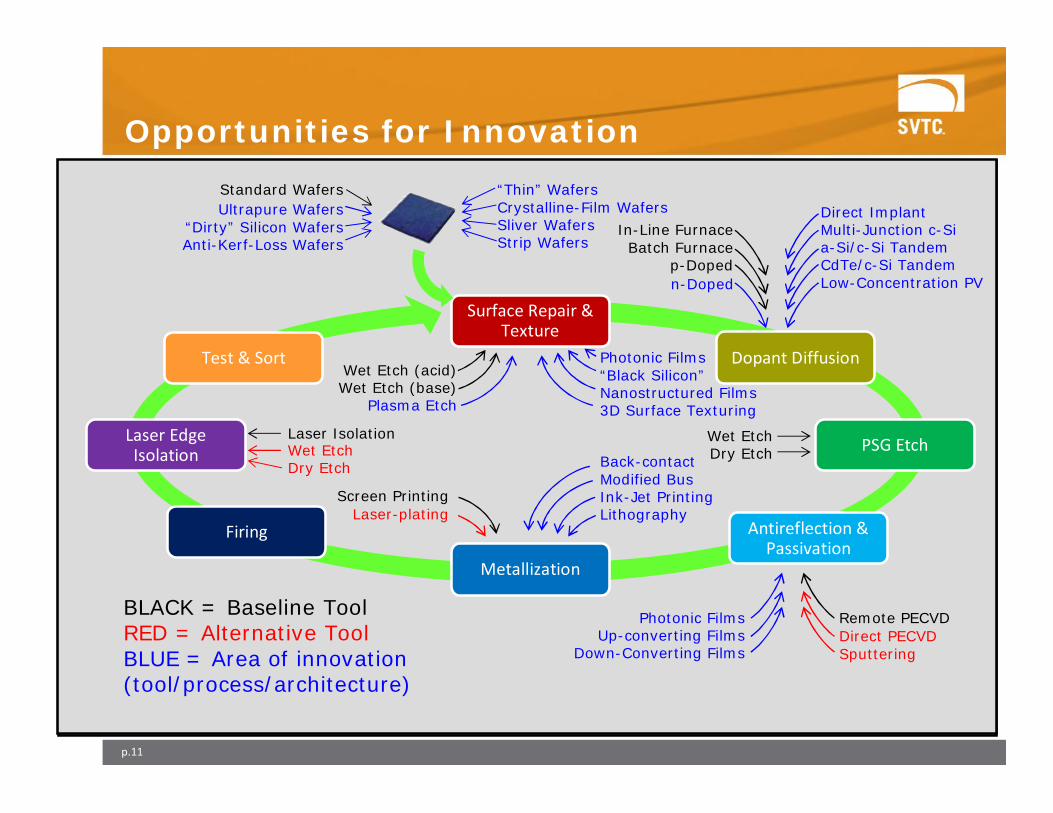
Opportunities for Innovation
p.11
Roth & Rau, USA30MW Baseline Tool Set
Roth & Rau, USA30MW Baseline Tool Set
Surface Repair & Texture
Dopant Diffusion
PSG Etch
Antireflection & Passivation
Metallization
Firing
Laser Edge Isolation
Test & Sort
Laser Isolation Wet EtchDry Etch
“Thin” WafersCrystalline-Film WafersSliver WafersStrip Wafers
Standard Wafers
Wet Etch (acid)Wet Etch (base)
Photonic Films“Black Silicon”Nanostructured Films3D Surface Texturing
In-Line FurnaceBatch Furnace
p-Doped
Direct ImplantMulti-Junction c-Sia-Si/c-Si TandemCdTe/c-Si TandemLow-Concentration PV
Remote PECVDPhotonic FilmsUp-converting Films
Down-Converting Films
Screen Printing
Back-contactModified BusInk-Jet PrintingLithography
Plasma Etch
Ultrapure Wafers“Dirty” Silicon WafersAnti-Kerf-Loss Wafers
Direct PECVDSputtering
Laser-plating
Wet EtchDry Etch
n-Doped
BLACK = Baseline ToolRED = Alternative ToolBLUE = Area of innovation (tool/process/architecture)
Surface Repair & Texture
Dopant Diffusion
PSG Etch
Antireflection & Passivation
Metallization
Firing
Laser Edge Isolation
Test & Sort
p.12
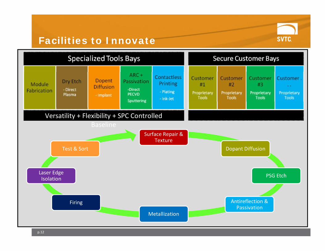
Facilities to Innovate
Versatility + Flexibility + SPC Controlled Baseline
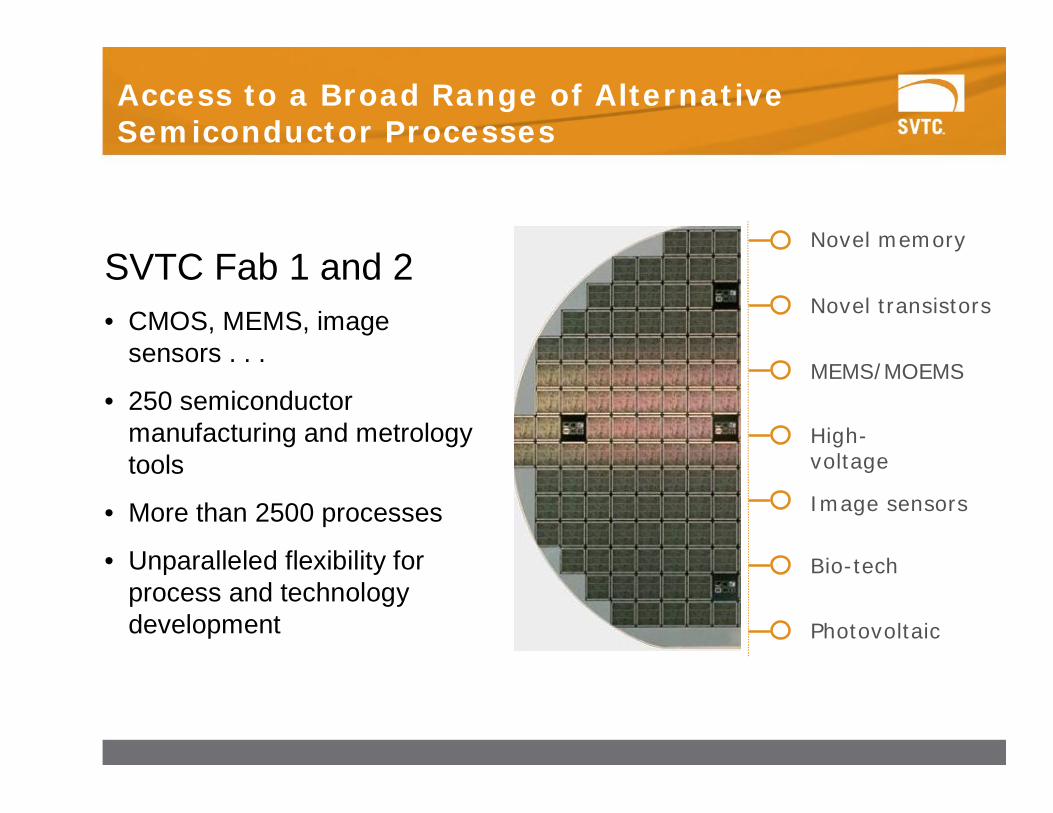
Novel memory
MEMS/MOEMS
Photovoltaic
High-voltage
Bio-tech
Novel transistors
Image sensors
Access to a Broad Range of Alternative Semiconductor Processes
SVTC Fab 1 and 2• CMOS, MEMS, image
sensors . . .
• 250 semiconductor manufacturing and metrology tools
• More than 2500 processes
• Unparalleled flexibility for process and technology development

Key Elements of a Solar Development Center
p.14
Not another research center
SVTC Solar
Manufacturing Tools
Manufacturing Focus
Manufacturing Staff
Manufacturing Controls
SVTC Solar
+ = Synergy
• Manufacturing Equipment
• Leverage Across Tools
• Flexibility to Innovate
• Manufacturing Expertise and “Culture”
• Alternative Materials
• Analytical Services
• IP Ownership/Security
• Many Types of Customers
Key Requirements

Key Elements of a Solar Development Center
p.15
Classic CMOS Fab Additional at SVTC
Li
Na
K
Rb
Cs
Fr
Be
Ra Ac
Ce
Th
Rf
Pr
Pa
Db
Nd
U
Sg
Pm
Np
Tc
Re
Bh
Sm
Pu
Os
Hs
Eu
Am
Rh
Mt
Cm Bk
Au
Cf
Cd
Hg
Ho
Es
Ga
Ti
Fm
Ge
Pb
Tm
Md
Bi
No
Lu
Lr
Br
I
At
F
Ci
H
Ti
W
Co Ni Cu
B
Al Si
As
N
P
O
Ar
Xe
Rn
Mg
Ca
Sr
Ba
Sc
Y
La
Zr
Hf
V
Nb
Ta
Cr
Mo
Mn Fe
Ru
Ir
Gd
Pd
Pt
Tb
Ag
Dy
Zn
In
Er
Sn
C
Sb
Yb
Te
S
He
Ne
Se Kr
Po
Mg
Ca
Sr
Ba
Sc
Y
La
Zr
Hf
V
Nb
Ta
Cr
Mo
Mn Fe
Ru
Ir
Gd
Pd
Pt
Tb
Ag
Dy
Zn
In
Er
C
Sb
Yb
Te
S
He
Bi
Ge
• Advanced materials are critical to solar innovation
• Working with novel materials isan SVTC core competency (52 elements run through CMOS lines)
• Many new materials will be added for solar development (customer driven)
Materials Currently Running in SVTC’s CMOS Facility
• Manufacturing Equipment
• Leverage Across Tools
• Flexibility to Innovate
• Manufacturing Expertise and “Culture”
• Alternative Materials
• Analytical Services
• IP Ownership/Security
• Many Types of Customers
Key Requirements
Key Elements of a Solar Development Center
p.16
• Manufacturing Equipment
• Leverage Across Tools
• Flexibility to Innovate
• Manufacturing Expertise and “Culture”
• Alternative Materials
• Analytical Services
• IP Ownership/Security
• Many Types of Customers
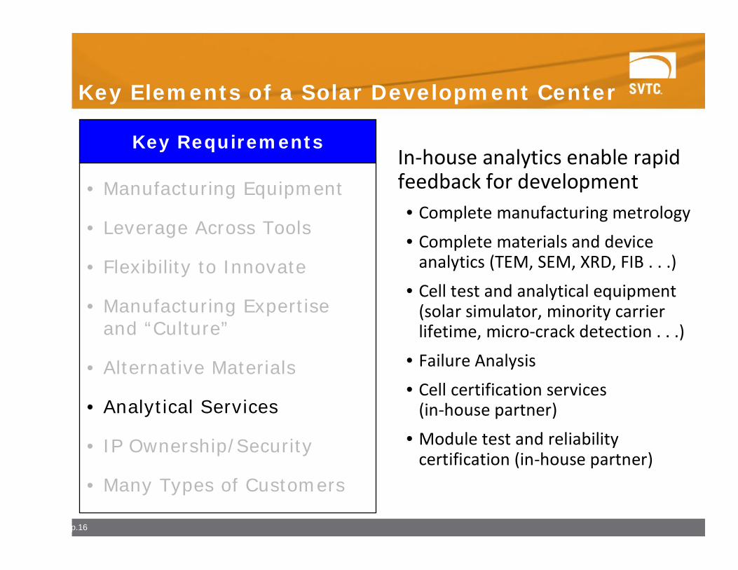
Key RequirementsIn-house analytics enable rapid feedback for development• Complete manufacturing metrology
• Complete materials and device analytics (TEM, SEM, XRD, FIB . . .)
• Cell test and analytical equipment (solar simulator, minority carrier lifetime, micro-crack detection . . .)
• Failure Analysis
• Cell certification services (in-house partner)
• Module test and reliability certification (in-house partner)
Key Elements of a Solar Development Center
p.17
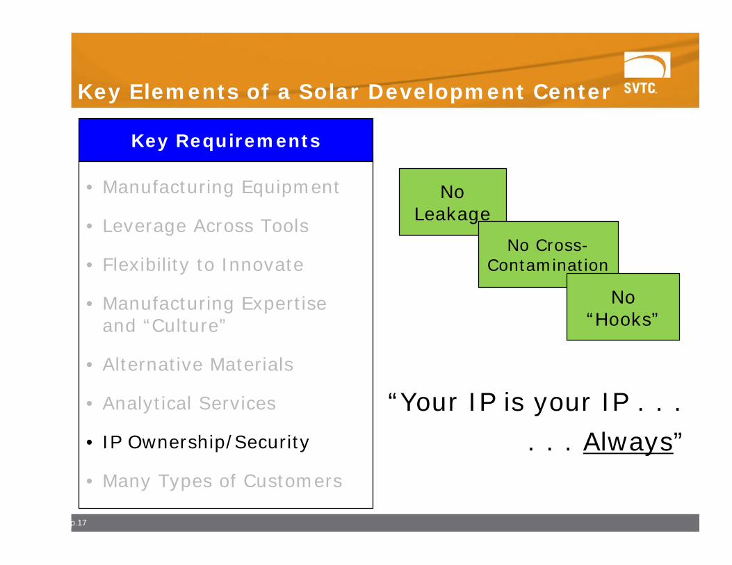
“Your IP is your IP . . .
. . . Always”
No Leakage
No Cross-Contamination
No “Hooks”
• Manufacturing Equipment
• Leverage Across Tools
• Flexibility to Innovate
• Manufacturing Expertise and “Culture”
• Alternative Materials
• Analytical Services
• IP Ownership/Security
• Many Types of Customers
Key Requirements
p.18
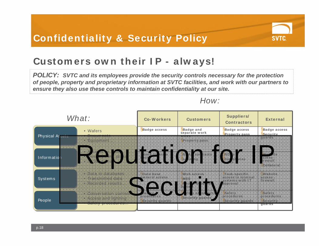
Confidentiality & Security Policy
Customers own their IP - always!POLICY: SVTC and its employees provide the security controls necessary for the protection of people, property and proprietary information at SVTC facilities, and work with our partners to ensure they also use these controls to maintain confidentiality at our site.
Physical AssetsPhysical Assets
Information Information
PeoplePeople
• Wafers• Documents• Equipment…
• Recipes on tools• Development plans• IP Solutions…
• Conversation content• Access and lighting• Safety procedures…
Systems Systems • Data in databases• Transmitted data• Recorded results…
Co-Workers CustomersSuppliers/ Contractors
External
§Badge access §Badge and separate work areas§Property pass
§Badge access§Property pass
§Badge access§Security guards
§Need-to-know basis§Labeling
§NDAs, contracts§Labeling
§NDAs§Compliance audits
§Website access -firewall§Collateral
§Data base owners/access
§Web access§MES§Recipe Security System
§Task-specific access to internal systems with IT approval
§Website access -firewall
§Safety procedures§Security guards
§Safety procedures§Security guards
§Safety procedures§Security guards
§Safety procedures§Security guards
What:
How:
Reputation for IP Security
Key Elements of a Solar Development Center
p.19
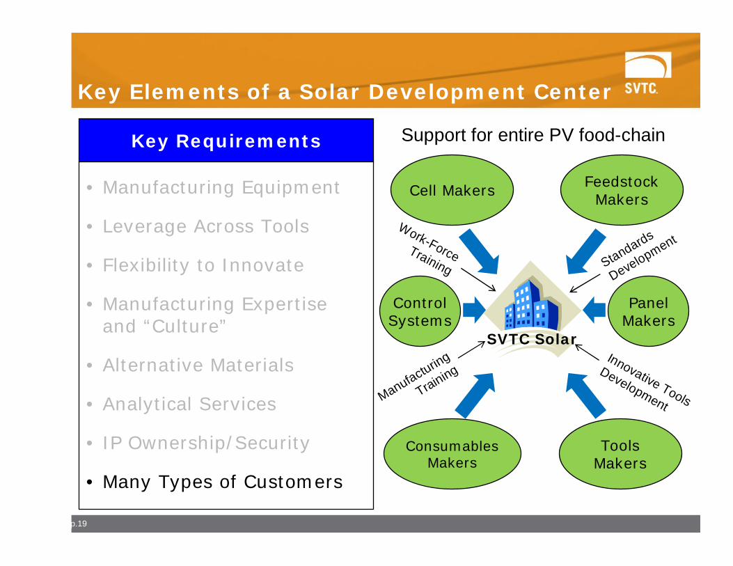
SVTC Solar
Cell Makers Feedstock Makers
Tools Makers
Consumables Makers
Support for entire PV food-chain
Panel Makers
• Manufacturing Equipment
• Leverage Across Tools
• Flexibility to Innovate
• Manufacturing Expertise and “Culture”
• Alternative Materials
• Analytical Services
• IP Ownership/Security
• Many Types of Customers
Key Requirements
ControlSystems
Work-Force Training
Manufacturing
TrainingInnovative Tools
Development
Standards
Development
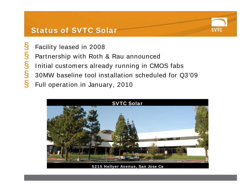
§ Facility leased in 2008§ Partnership with Roth & Rau announced§ Initial customers already running in CMOS fabs§ 30MW baseline tool installation scheduled for Q3’09§ Full operation in January, 2010
Status of SVTC Solar
SVTC Solar
5215 Hellyer Avenue, San Jose Ca
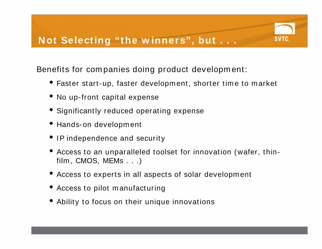
Not Selecting “the winners”, but . . .
Benefits for companies doing product development:
• Faster start-up, faster development, shorter time to market
• No up-front capital expense
• Significantly reduced operating expense
• Hands-on development
• IP independence and security
• Access to an unparalleled toolset for innovation (wafer, thin-film, CMOS, MEMs . . .)
• Access to experts in all aspects of solar development
• Access to pilot manufacturing
• Ability to focus on their unique innovations
p.21

www.svtc.com
Steve Empedocles
Director of Business Development, Solar Division
650-776-7089
p.22
SVTC SolarA Photovoltaic Product Development Center