Embed Size (px)
Citation preview
REPORT OFDEPARTMENT OF DEFENSE
0 ADVISORY GROUP ON ELECTRON DEVICESWORKING GROUP B (MICROELECTRONICS)
SPECIAL TECHNOLOGY AREA REVIEW
ON
SPINTRONICS
20060208 139
0i
0 19 UTI O STAT71 1ET AJune 2004 APpprovcd for Public Release
Distribution Unlimited
OFFICE OF THE UNDER SECRETARY OF DEFENSEACQUISITION, TECHNOLOGY & LOGISTICS
WASHINGTON, DC 20301-3140
CLEAREDFOR OPEN PUBLICATION
6AUG 3 2004 9
OFFICE OF FREEDOM OF INFORMATIONAND SECURITY REVIEW
DEPARTMENT OF DEFENSE
S
S
THIS REPORT IS A PRODUCT OF THE DEFENSE ADVISORY GROUP ON ELECTRON DEVICES (AGED). THE AGED IS AFEDERAL ADVISORY COMMITTEE ESTABLISHED TO PROMOTE INDEPENDENT ADVICE TO THE OFFICE OF THE DIRECTOROF DEFENSE AND ENGINEERING. STATEMENTS, OPINIONS, RECOMMENDATIONS, AND CONCLUSIONS IN THIS REPORTDO NOT NECESSARILY REPRESENT THE OFFICIAL POSITION OF THE DEPARTMENT OF DEFENSE.
Prepared by the AGED SecretariatPalisades Institute for Research Services, Inc.241 1 8 1h Street, Suite 500, Arlington, VA 22202
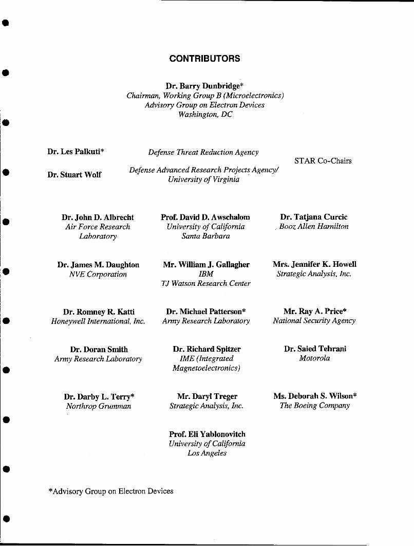
CONTRIBUTORS
Dr. Barry Dunbridge*Chairman, Working Group B (Microelectronics)
Advisory Group on Electron DevicesWashington, DC
Dr. Les Palkuti* Defense Threat Reduction AgencySTAR Co-Chairs
Dr. Stuart Wolf Defense Advanced Research Projects Agency!University of Virginia
Dr. John D. Albrecht Prof. David D. Awschalom Dr. Tatjana CurcicAir Force Research University of California Booz Allen Hamilton
Laboratory Santa Barbara
Dr. James M. Daughton Mr. William J. Gallagher Mrs. Jennifer K. HowellNVE Corporation IBM Strategic Analysis, Inc.
TJ Watson Research Center
Dr. Romney R. Katti Dr. Michael Patterson* Mr. Ray A. Price*Honeywell International, Inc. Army Research Laboratory National Security Agency
Dr. Doran Smith Dr. Richard Spitzer Dr. Saied TehraniArmy Research Laboratory IME (Integrated Motorola
Magnetoelectronics)
Dr. Darby L. Terry* Mr. Daryl Treger Ms. Deborah S. Wilson*Northrop Grumman Strategic Analysis, Inc. The Boeing Company
Prof. Eli YablonovitchUniversity of California
Los Angeles
*Advisory Group on Electron Devices
DEPARTMENT OF DEFENSEADVISORY GROUP ON ELECTRON DEVICES (AGED)
WORKING GROUP B (MICROELECTRONICS)
SPECIAL TECHNOLOGY AREA REVIEWON
SPINTRONICS
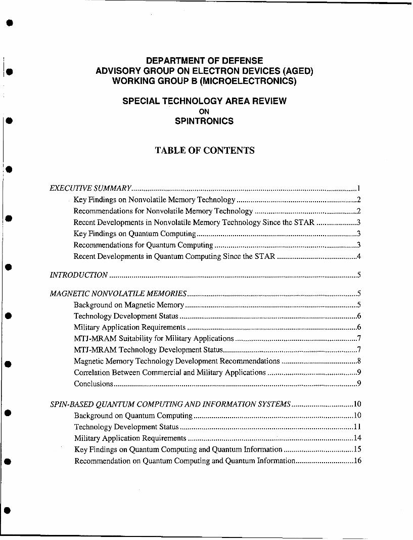
TABLE OF CONTENTS
EXECUTIVE SUM MARY ....................................................................................................... 1Key Findings on Nonvolatile Memory Technology ...................................................... 2Recommendations for Nonvolatile Memory Technology ............................................ 2Recent Developments in Nonvolatile Memory Technology Since the STAR .............. 3Key Findings on Quantum Computing ........................................................................... 3Recommendations for Quantum Computing ................................................................. 3Recent Developments in Quantum Computing Since the STAR ................................... 4
IN TR O D U C TIO N ............................................................................................................................ 5
MAGNETIC NONVOLATILE MEMORIES ................................................................................ 5Background on M agnetic M emory ............................................................................... 5Technology Developm ent Status .................................................................................... 6M ilitary Application Requirements ............................................................................... 6MTJ-MRAM Suitability for Military Applications ........................................................ 7MTJ-MRAM Technology Development Status ............................................................. 7Magnetic Memory Technology Development Recommendations ................................. 8Correlation Between Commercial and Military Applications ........................................ 9C onclusions .......................................................................................................................... 9
SPIN-BASED QUANTUM COMPUTING AND INFORMATION SYSTEMS ........................... 10Background on Quantum Computing ........................................................................... 10Technology Developm ent Status .................................................................................. 11M ilitary Application Requirements ............................................................................. 14Key Findings on Quantum Computing and Quantum Information .............................. 15
Recommendation on Quantum Computing and Quantum Information ......................... 16
FIGURES:The State of Play ................................................................................................................ 12
N uclear M agnetic Resonance ....................................................................................... 12
Ion Traps ............................................................................................................................ 13Superconducting Josephson Junctions .......................................................................... 13Silicon Q uantum Com puting ........................................................................................ 14
APPENDICES:
Appendix A: Quantum Information Science Landscape .............................................. 17A ppendix B : Term s of Reference ................................................................................. 23
A ppendix C : A genda .................................................................................................... 27
ACRO YNM S ................................................................................................................................... 29
t0
i0
DEPARTMENT OF DEFENSEADVISORY GROUP ON ELECTRON DEVICES (AGED)
WORKING GROUP B (MICROELECTRONICS)
SPECIAL TECHNOLOGY AREA REVIEWON
SPINTRONICS
EXECUTIVE SUMMARY
The objective of this Advisory Group on Electron Devices (AGED) Working Group B(Microelectronics) Special Technology Area Review (STAR) was to examine the status ofspintronics (electronics based on the spin degree of freedom of the electron) as it applies tononvolatile memories and quantum-based logic and computing. In addition, the informationprovided at the STAR is expected to be of use to the Services and Department of Defense (DoD)agencies as they formulate an investment strategy for realizing the potential benefits of spin-based technologies for military applications. For example, magnetic tunnel junction (MTJ) basednonvolatile memory has the potential to replace dynamic random access memory (DRAM) andfloating-gate nonvolatile memory (Flash). Specifically the objectives of the STAR were to:
e Evaluate the present status and progress in spin-based nonvolatile memory applications.* Determine the military applications of this disruptive memory technology particularly as it
relates applying the technology in space-based applications.* Review the potential for spin qubit-based quantum logic and computing.* Identify current technical barriers and impediments; and possible breakthroughs in quantum
spin-based computing technologies for future military system applications.• Develop additional science and technology efforts to expand applications to DoD systems.
The STAR was convened at the Fess Parker's DoubleTree Resort, Santa Barbara, CA on March19, 2003. A distinguished group of speakers made presentations as follows: from industry onnonvolatile memory technology, from universities on quantum computing and communicationsand from the Defense Advanced Research Projects Agency (DARPA) on the militaryapplications of spin-based computing. In addition, a university speaker summarized theworldwide efforts in quantum information research. The speakers also participated in two paneldiscussions that interacted extensively with the AGED Working Group B membership and otherattendees at the STAR, answering questions and discussing research needed to expand themilitary applications of spin-based nonvolatile memories and spin-based quantum computing.
This STAR was held in conjunction with a DARPA workshop on quantum computing andquantum information processing where some of the same presentations were made. Thisworkshop was intended to define the type and scope of future research in this area. Based on thisworkshop and other workshops conducted this past year, DARPA has continued work in thisarea.

0
The following key findings and recommendations emerged from speakers' presentations andsubsequent discussions with the AGED Working Group B membership.
Key Findings on Nonvolatile Memory Technology
The development of magnetic nonvolatile memory technologies, especially the MTJ magneticrandom access memory (MRAM) is quite advanced. MTJ-MRAM can theoretically beoverwhelmingly better than Flash and other nonvolatile memories in terms of system 0friendliness. Unlike Flash, MTJ-MRAM has unlimited read/write cycles. MTJ-MRAIV iscurrently competitive in terms of power consumption and access performance with other non-volatile memories but MRAM has the highest write speed. Commercial MRAM products arebeing sampled this year. 6Some specific findings are:* The most advanced industry MRAM efforts are in the MTJ-MRAM area.* Motorola appears to be closest to commercializing a product - a 4Mb MTJ-MRAM. This
memory product utilizes the new Savtchenko switching mode and thus eliminates the half-select problem. 6
* IBM is developing two potential products in parallel: one classical matrix configuration witha selection transistor for each cell and one cross-point configuration, which does not requirethe active selection element. The former will have higher performance, the latter promisessignificantly higher densities.
* NVE is conducting development of magnetic (giant magneto resistive (GMR) and MTJ)sensors with military applications such as unattended sensors for vehicle or troop movementand non-destructive evaluation sensors for faults on airplane wings.
Recommendations for Nonvolatile Memory Technology
In order to achieve the DoD goal of developing nonvolatile memory components that fulfillmilitary application requirements, the following are recommended:
Investment in resolving the problems of the MTJ-MIRAM technologies:(a) The need to develop new write strategies such a spin momentum transfer, which will allow
write currents to shrink as manufacturing geometry shrinks. If these efforts are not pursuedthe consequences may be increasing per bit power consumption with increasing density.
(b) The need to combine a radiation-hard complementary metal oxide semiconductor (CMOS)under layer with the MTJ cell is now being addressed in a licensing arrangement betweenHoneywell and Motorola. This arrangement and others like it should be encouraged.
(c) The need to continue improvement in high reliability processes and make technologyavailable for trusted military applications.
Investment in the development of other alternative magnetic memory technologies such as the allmetal SpinRAM and the technology of spin momentum transfer.
-2-
Recent Developments in Nonvolatile Memory Technology Since the STAR
Honeywell and Motorola have a joint development program underway to demonstrate aradiation-hard 1Mb MTJ-MRAM that incorporates Honeywell's radiation hard 0.15micronCMOS silicon-on-insulator (SOI) technology with Motorola's latest MTJ cell. The MTJ layerswill be deposited on the CMOS SOI wafer after the third metal level. NVE is developing amagneto-thermal GMR technology that has significantly reduced write current by takingadvantage of either Curie or Niel point. In addition, Cypress is planning MRAM product releases(64k and 256k MRAM devices aimed at substituting battery backed-up static random accessmemory (SRAM)).
Key Findings on Quantum Computing
Quantum computing and quantum information technologies are promising solutions to a numberof critical problems of interest to the military and to commercial enterprise. At the time of thisreview, no implementation technology for a quantum computer has emerged as a clear leader inthis technically challenging field. There has, however, been great progress on several key basiccomponents.
Some specific findings are:"* Electrical control of spin coherence has been demonstrated at the basic level. This has been
done mainly through the gating of spin-engineered nanostructures.* Femtosecond operation (control over the setting and changing of quantum mechanical states)
has been demonstrated. Quantum repeaters for distributing quantum information have not yetbeen demonstrated but represent an important technology research area for nearly all of theimplementations in the quantum computing or quantum information fields.
"* Applications in computing include the factoring of very large numbers, the simulation oflarge quantum systems, unsorted database searching, complex scheduling, image processing(target recognition) and signal processing.
"* Novel DoD applications of quantum information science include optical detector absolutecalibration, absolute radiance measurements, single photon sources (and detectors), andenhanced lithographic techniques to reach below the diffraction limit using entangledphotons.
"* The main challenges facing this technology are decoherence, signal attenuation, limitedalgorithm development, and scalability.
"* A "race" among worldwide efforts is underway. An extensive reporting of the funding andactivity in this field (as of January 2003) was presented that shows a strong effort by foreigngovernments to fund their researchers to compete in this area.
Recommendations for Quantum Computing
The principal recommendation of this STAR is that an enormous effort in basic research is goingto be required to realize and implement a quantum computer or information system with real-world applications suitable to a military platform. Continued strong support from the DoD in thisarea is crucial. The challenges to building a successful system are enormous and will not happenthrough loose collaborative efforts among academicians applying for a series of small grants.
-3-
Strong support of systematic development, such as that suggested by the DARPA FoQuSprogram, is the way to leverage the efforts to date so that the computing implementations can beexplored more fully. A clear message from this STAR was that the rest of the world is not goingto stop development of quantum information systems for secure communications and quantumcomputers and there is a significant risk of the US falling behind.
Recent Developments in Quantum Computing Since the STAR
The DoD has shown a strong interest in the successful demonstration of a quantum computerwith the objective to have a systems-engineering approach to building a quantum computer withnarrow, targeted goals in the next five to ten years.
0
6
i6
--
-4-

DEPARTMENT OF DEFENSE* ADVISORY GROUP ON ELECTRON DEVICES (AGED)
WORKING GROUP B (MICROELECTRONICS)
SPECIAL TECHNOLOGY AREA REVIEWON
* SPINTRONICS
INTRODUCTION
Spintronics (electronics based on the spin degree of freedom of the electron) is of great current0 interest and has the potential to revolutionize current charge based electronics. For example
magnetoresistive (GMR and MTJ)-based nonvolatile memory has the potential to replace Flashand dynamic random access memory (DRAM). It is timely to provide AGED and the Office ofthe Secretary of Defense with an up-to-date assessment of the military applications in this field.
MAGNETIC NONVOLATILE MEMORIES
The purpose of this section is to provide a summary of the presentations and the discussions held*0 during the STAR about magnetic nonvolatile technologies and their suitability for military
applications. It is structured as follows: 1) background on magnetic nonvolatile memory, 2)technology development status, 3) memory requirements for military applications, 4) the extentto which MTJ-MRAM will satisfy these requirements, 5) magnetic memory developments, and6) future magnetic technology developments,.
Background on Magnetic Memory
Magnetic memories have the potential to become valuable alternative technologies for electroniccomponents. Research to date indicates that electronic memory components based on magnetismhave the capability to improve system performance and reduce system costs. In addition, these
* components are nonvolatile, and their magnetic portions are radiation hard.
Although there are a multitude of magnetic nonvolatile memory approaches, all MRAM deviceshave a series of common characteristics. All rely on merging two very different technologies:1) a semiconductor base for an active cell array matrix and ancillary circuitry and 2) a
* magnetically sensitive storage cell built as a combination of magnetic and semiconductormaterials. The storage cell is a multi-layer structure, e.g. magnetic tunnel junction that changesits magnetization state when a certain magnetic field combination is applied to it via currents inneighboring wires. The cell transistor in the array allows selecting the cell for reading. "Bitdisturb" defines the phenomenon of corrupting the content of a cell that has been selected non-intentionally along one of the two simultaneously activated half-select current lines that providethe magnetic field for writing.
-5-
The major difference between the different types of memories comes from the structure of thestorage cell. So far, four different techniques have been employed for storing magnetic ginformation in the cell: 1) AMR (anisotropic magnetoresistance), 2) GMR (giantmagnetoresistance), 3) MTJ (magnetic tunnel junction), and 4) CMR (colossalmagnetoresistance).
Technology Development Status
For technology reasons (magnetic state discrimination signal too small), AMR based memorieshave not evolved into the commercial market. GMR based memories have been productized on avery limited basis, but not commercialized. They have a higher discrimination signal than AMR,which allows developing usable memory components. The exploitation of the magnetictunneling effect has created new perspectives. Unlike GMR, MTJ cells require perpendicularlyflowing currents. In addition, they generate a much higher output signal. The former attributeallows building compact cell array matrices, while the latter reduces the complexity of thesensing circuitry. In the last five years, nearly all industry research and productization effortshave been concentrated on MTJ. Finally, an all-metal SpinRAM technology based on the GMReffect is in the basic development stage. Its main promise is a low cost silicon-free technology 0that is inherently radiation hard.
The specific MRAM efforts discussed at the STAR included (presentation charts are availablefrom the AGED Secretariat):"* Romney Katti, Honeywell, "GMR MRAM with Current-in-Plane Magnetic Devices""* Saied Tehrani, Motorola, "Tunnel Junction MRAM Technology""* Jim Daughton, NVE, "GMR Memory and Sensors with Spin-Dependent Tunneling
Technology""* Bill Gallagher, IBM, "Magnetic Tunnel Junction MRAM""* Richard Spitzer, Integrated Magnetoelectronics (IME), "All-Metal GMR-Based SpinRAM"
Military Application Requirements
Nonvolatile memory components for military missile and space applications require:"* Radiation hardness"* Fast read/write performance"* High density"* Low power"* Long endurance"• Random access capability"* Trusted on-shore fabrication
-6-
MTJ-MRAM Suitability for Military Applications
Compared with other memory technologies, MTJ-MRAM has a series of inherent advantages formilitary applications:"* The magnetic storage cell is radiation hard; however, the semiconductor base is radiation
vulnerable. In order to achieve radiation hardness combining the radiation hard magneticdevice with a radiation-hard CMOS process is required. Since there is a clear isolationbetween the CMOS and magnetic components, combining rad hard CMOS with MTJ cells isfeasible.
"* The density (defined as normalized capacity) of MTJ-MRAM components is determined bythe semiconductor technology node. Because every cell needs an active element (transistor ordiode) for selection, the cell size can approach 4f2. This results in a storage density that iscomparable with that of NAND Flash with 1-bit per cell, which is approximately 1.5 Gb/cm2.
" The power consumption of MTJ-MRAM can be theoretically lower than that of puresemiconductor memories, mainly because of lower leakage and better stand-by currents.
"• MTJ-MRAM, like NOR Flash and trapped charge devices, has full random access capability."• The MTJ-MRAM access performance is generally comparable with that of DRAM and MTJ-
MRAM has the fastest write time of all nonvolatile technologies."* "System friendliness" measures the hidden system costs introduced by a technology. These
costs are generated by additional hardware or software that is needed to compensate for thetechnology limitations, such as asymmetric access, low access performance, limitedendurance, or volatility. On a comparative basis, MTJ- MRAM components are much moresystem friendly than Flash and trapped charge memory components.
In summary: MTJ-MRAM memories can be overwhelmingly better than Flash and other non-volatile memories in terms of system friendliness. Unlike Flash, MTJ-MRAM has unlimitedread/write cycles. The MTJ memory cell itself is radiation hard but must be combined with aradiation-hard CMOS process. MTJ-MRAM is at equal terms of power consumption and accessperformance and MRAM has the highest write speed compared to other nonvolatile memories.
MTJ-MRAM Technology Development Status
e The most advanced industry MRAM efforts are in the MTJ-MRAM area.* Motorola is closest to commercializing a product. A 4Mb MTJ-MRAM component was
described at the 2003 IEDM (Durlam, et al, "A 0.18micron 4Mb Toggle MRAM", 2003IEDM Technical Digest, paper 34.6). This memory product utilizes the new Savtchenkoswitching mode and thus eliminates the half-select problem.
9 Honeywell and Motorola have a joint development program underway to demonstrate aradiation-hard 1Mb MTJ-MRAM that incorporates Honeywell's radiation hard 0.15micronCMOS/SOI technology with Motorola's latest MTJ toggle cell. The MTJ layers will bedeposited on the CMOS SOI wafer after the third metal level.
9 IBM is developing two potential products in parallel: one classical matrix configuration witha selection transistor for each cell and one cross-point configuration, which does not requirethe active selection element. The former will have higher performance, the latter promisessignificantly higher densities. Both developments appear to be'behind schedule, probablybecause of bit disturb and write current problems. IBM is trying to solve the select problem
-7-
by building "twin cells" that use two adjacent cells to store one bit, which doubles the signalsand cancels noise, but reduces the density by 50%. It is not known how much time it will take gto fix the problems. Also the write current scalability appears to be a fundamental problem.
" NVE is conducting development of magnetic (GMR) sensors with military application suchas unattended sensors for vehicle or troop movement and non-destructive evaluation sensorsfor faults on airplane wings.
"* NVE is developing a magneto-thermal GMR technology that has significantly reduced writecurrent by taking advantage of either Curie or Niel point.
" Cypress is still planning MRAM product release (device aimed at substituting batterybacked-up SRAM) in collaboration with NVE to sample in late 2004. Cypress has recentlyreleased data sheets on two MRAM products (64k and 256k MRAM).
To date, some issues with the MTJ technology have become evident: •* MTJ based cells have open flux structures for which coercivity increases with decreasing cell
size, which leads to increased write currents. While Motorola claims to have partially solvedthe problem through cladding, none of the others have made any progress in this area. TheMotorola solution just ameliorates the effect, it does not eliminate it. It also appears that theperpendicular current structure required by the MTJ cell, which is an attractive feature formatrix type structures, does not lend itself to create a totally closed flux cell structure, whichprevents write currents from scaling in phase with the manufacturing geometry. Instead, writecurrents are increasing as geometry shrinks.
* The open flux structure creates the danger to influence adjacent cells. To prevent this, openflux cells have to be wider spaced. As a result, the real cell size is about 20f2, approximately5 times bigger that the theoretical size (4f2), which leads to a similar reduction of thecomponent density. In addition, the overhead circuits in MRAM significantly limit density.
* A further problem appears to be the processing of the very thin films required by the MTJcell. Motorola and IBM appear to be the most advanced in developing a manufacturingprocesses that will increase quality and yields. The efficiency of this process is paramount for •creating high performance system-on-chip configurations.
Magnetic Memory Technology Development Recommendations
In order to achieve the DoD goal of developing nonvolatile memory components that fulfillmilitary application requirements the following are recommended:
Investment in resolving the problems with the MTJ-MRAM technologies:(a) The need to develop new write strategies such as spin momentum transfer, which will allow
write currents to shrink as manufacturing geometry shrinks. If these efforts are not pursuedthe consequences may be increasing per bit power consumption with increasing density.
(b) The need to combine radiation-hard CMOS/SOI under layer with the MTJ cell is now beingaddressed in a licensing arrangement between Honeywell and Motorola. This arrangementand others like it should be encouraged.
(c) The need to continue improvement in high reliability processes and make technologyavailable for trusted military applications. (See IBM white paper entitled "MRAM 6Development for Space Mission Memory Subsystems" September 2003, available from theAGED Secretariat).
-8-
Investment in the development of other alternative magnetic memory technologies such as theall-metal SpinRAM and the technology of spin momentum transfer.
The all-metal SpinRAM is being developed by IME. According to their presentation, in additionto all MTJ-MRAM advantages, SpinRAM offers inherent radiation hardness, the potential for anup to two orders of magnitude increase in density, much above the mechanic-magnetic HDDlevel, as well as a two orders of magnitude decrease in power consumption. If the technologyfulfills the claims IME makes, it appears to be the ideal solution for discrete memorycomponents, embedded memory components and system-on-a-chip solutions. The latter ispossible because the technology allows for building not only storage cells based on the spineffect, but also system logic elements like digital logic (the foundation for microcontrollers andmicroprocessors) and analog circuitry. The potential of the SpinRAM technology should beinvestigated in detail to assess its potential. (See white paper by J. Spitzer, IME, entitled"Integrated Magnetoelectronics -All-Metal Electronics" April 2003, available from the AGEDSecretariat).
Correlation Between Commercial and Military Applications
Military requirements for electronic components in general and for nonvolatile memories inparticular are technologically much more demanding than commercial applications. Thenonvolatile memory military requirement that is not mandatory for the vast majority ofcommercial applications is radiation hardness. Even so, military applications will greatly benefitfrom utilizing technologies with commercial applications, not only because of the larger R&Dbase, but also because of the quality improvement brought about by the very large manufacturingvolumes and the higher technology improvement pace.
Conclusions
The development of magnetic memory technologies, especially MTJ-MRAM, is quite advanced.The first commercial products are being sampled this year. The next step is to create a military-grade component (to be applied to the D5 missile life extension program) by replacing the MTJ-MRAM commercial bulk CMOS base with a radiation-hard CMOS/SOI technology. In addition,the development of methods to reduce the current drive requirements for the MTJ-MRAMtechnology, such as the magneto-thermal technology, should be continued. The all-metalSpinRAM technology is theoretically capable of producing beneficial nonvolatile memory.There is a value in further investigating this technology.
S -9-
0
SPIN-BASED QUANTUM COMPUTING AND INFORMATION SYSTEMS0
The purpose of this section is to provide a summary of the presentations and the discussions heldduring the STAR about spin-based quantum computing technologies and their suitability formilitary applications. It is structured as follows: 1) background on quantum computing andquantum information, 2) technology development status and recent developments, 3)requirements for military applications, 4) key findings, and 5) recommendations.
Background on Quantum Computing
Quantum computers offer the potential to solve certain classes of computationally intensiveproblems that would be prohibitively difficult (or impossible) using standard computingmethods. These problems include the factorization of large integers, database searching, thesimulation of quantum mechanical effects and, more generally, other problems described bypartial differential equations. Although there are many candidate approaches to building aquantum computer, the central theme is the entanglement of quantum bits, or qubits. It is usefulto begin with a comparison to standard digital computing.
Almost all of today's computers are based on simple Turing Theory and employ Boolean logicbased on binary mathematics. Even "parallel" computers are really complex Turing enginesemploying multiple computing modules, which deal with pieces of incoming data (chunks, bytes,instructions, etc.). There has been some research into biological computing using enzymes orlarge-molecule systems as memory, shift registers, etc., but this has not proven to be verypractical.
Where the digital computer uses binary digits (bits), the quantum computer uses qubits, butqubits are extremely difficult to generate. Quantum computing is based on a different physicsthan digital computing. Instead of having two states-per-element like digital computers, whichare off or on, quantum computers can have all three states at the same time. A classical 8-bitdigital computer can exist in only one of 256 states at a time while an eight bit quantumcomputer can exist in a linear superposition of all 256 states at a time and theoretically, quantumoperation works on 256 calculations at once (quantum parallelism). Each of the 256 numbers inthis 8-bit example can, if the register is initiated appropriately, have an equal probability of beingmeasured so that a quantum processor can functions as a random number generator. The actualregister is representing all of these values at once but a single value output only occurs atmeasurement. While a classical digital computer would have to operate on each number from 0to 255, quantum computers require only one pass through the "processor," radically reducingcalculation time. Of course, the larger the register size, the larger the number - even a simple 20-bit quantum computer could scream past a supercomputer for an appropriate problem likefactoring.
A quantum switch must be undisturbed. The impinging fields required for the proper operationof a quantum computer depend on the interaction of the various qubits without any outsideinfluence. When disturbed, the qubit becomes quite Newtonian rather than quantum and selects adefinite state - by chance becoming, dare we say, digital. Paul Benioff of the Argonne NationalLaboratory first applied quantum theory to computers in 1981 and David Deutsch of Oxford
-10-
proposed quantum parallel computers in 1985, years before the realization of qubits in 1995.Qubits are made using various techniques. A group at the National Institute of Standards inBoulder, CO trapped a single atom with missing electrons (an ion) with two energy levels bycontaining it with magnetic and electric fields at -273 degrees C. Another group at CaliforniaInstitute of Technology made qubits from polarized light using a device, which allows photons tointeract while they pass though a stream of cesium atoms interacting in a XOR-like manner. AtLos Alamos, researchers make qubits by trapping ions. Ion traps, housing up to six ions, havealready been produced - far short of the thousands required for a useable quantum computer.
Although quantum computers at the system level (beyond a few qubits or a gate) have not beenbuilt to date, many of the mechanisms required, like error correction and algorithm construction,are being investigated. Because of their multiple states (unlike two-state digital processes)quantum computers will have some of the problems that analog computers had - namely errorcorrection and calculation reliability (although this does not sound very quantum mechanical).Physicists are arguing what type of error correction will work with qubits and quantummeasurement in general. John von Neuman's work in computer error detection and correction isbeing re-examined and has led to new efforts in quantum error correction. The samesuperposition that gives quantum computation its parallelism may give quantum error correctionits power dramatically exceeding classical error correction methods.
For additional background information see Quantum Computation and Quantum Information byM. A. Nielson and I. L. Chuang. Cambridge University Press, September 2000.
Technology Development Status
Quantum computing has been tested or proposed in several physical systems. Here is a brief listof the leading candidates followed by some highlighted examples."* Liquid State NMR and NMR Spin Lattices"* Linear Ion-Trap Spectroscopy"* Neutral Atom Optical Lattices"* Cavity QED"* Linear Optics with Single Photons"" Nitrogen Vacancies in Diamond"* Electrons in Liquid Helium"* Small Josephson Junctions"* Spin Spectroscopies"* Coupled Quantum Dots
* -11-
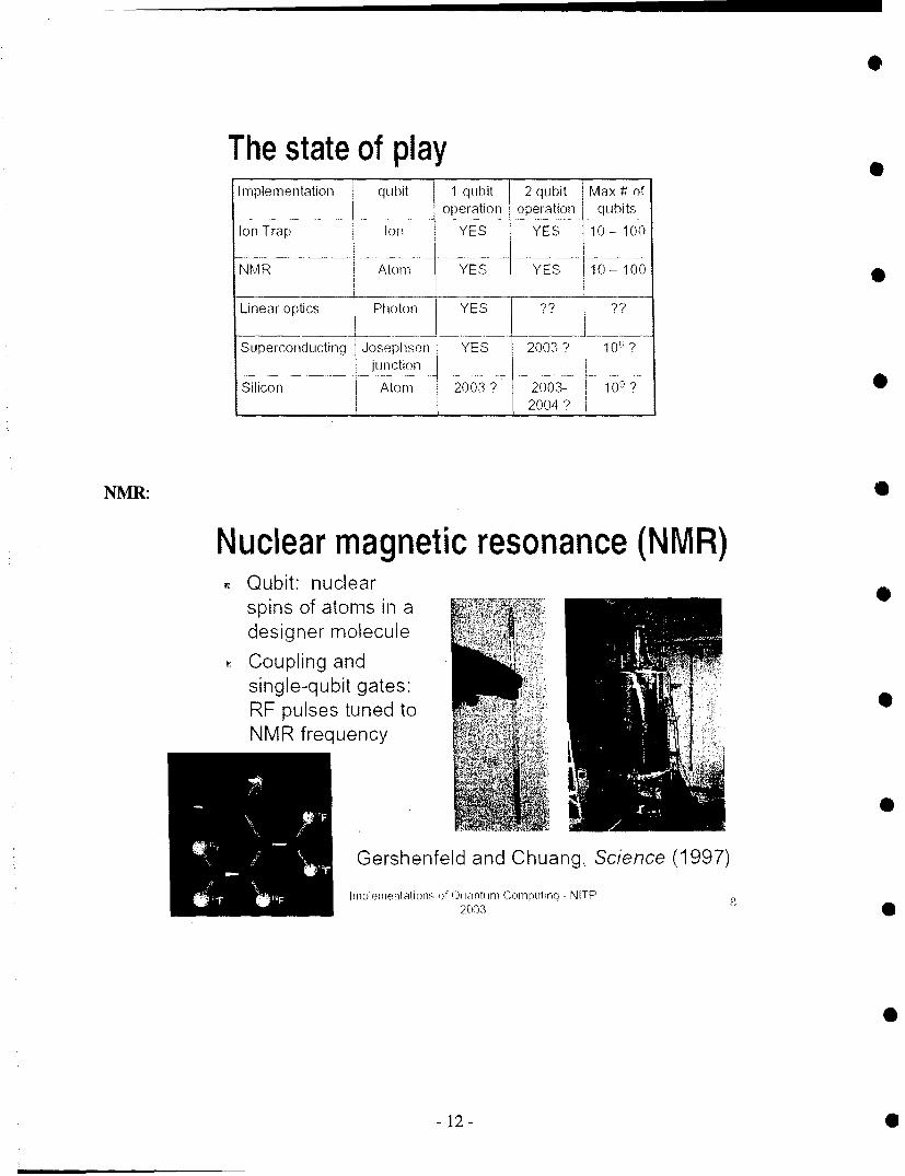
The state of play
1 mplemnen tation F qtuhit 1 quhit 2 qubit Max ft of____________ope ratio n opera.tion -qubits--
Ion Trap Ion YES YES 10 1 00
NMR IAtom YES YES 10- 100
Linear optics Photon YES ???
Superconfducing IJosephson YES 2003 ? 10(, ?____________________ jUnCtiOrln
Silicon Atom 2003 ? 2003- 10 O7 ?1________ 2004 ?
NMR:
Nuclear magnetic resonance (NMR)Qubit: nuclearspins of atomns 'in adesigner moleculeCoupling andsingle-qubit gates:PF pulses tuned toNMR frequency
Gershenfeld and Chuang, Scienice (1997)
mi: eieni~ii n~of Qua ntum C em puti ng - N ITP
20010

Ion Traps:
Ion traps
Qubit: internal* electronic state of
atomic ion in a trap(ground and excited)
SCoupling: usequantised vibrationalmode along linear axis(phonons)
* Single qubit gates:using laser
Cirac and Zoller, Phys. Rev. Lett. (1995)
Josephson Junctions:
Superconducting Josephson* junctions
Qubit: a) Magnetic flux trapped in loop
b) Cooper pair charge on metal box
c) Charge-phase
Coupling: capacitive/inductive
It Single-qubit gates: flux bias, charge on gate,current through junction
* Nakamura,Pashkin, Tsai,Nature (1999)
-13-

Silicon:
Silicon quantum computingQubit:"* Nuclear spin of single P donor T Z I V
"* Electron spin of single donor
"* Electron charge
Coupling: gate-controlledelectron-electron interaction _,_
Single-qubit gates: NMR pulse;gate bias in magnetic material;-charge on gate
QUANTUM COMPUTER Kane, Nature (1998)
The specific quantum computing efforts discussed at the STAR included (see presentation charts,available from the AGED Secretariat):"* David Awschalom, UCSB "Spintronics for Logic, Storage, and Computing""* Eli Yablanovich, UCLA "Quantum Information Processing Using Spins in Semiconductors""* Stuart Wolf, DARPA "Quantum Information Science and Technology""* Tatjana Curcic, Booz Allen Hamilton "Quantum Information Science Landscape." An
extensive reporting of the funding and activity in this field (this briefing outlines researchefforts as of January 2003 and the authors noted that significant changes in the researchlandscape has occurred during the past year) was presented and is included here at the end ofthis report in Appendix A. This briefing shows a strong effort by foreign governments tofund their researchers to compete in this area.
Military Application Requirements
Military applications include:"* Factorization (code breaking)"* Searching (pattern recognition, huge database searches, etc)"* Image and signal processing using generalized transforms"* Powerful simulations of large non-linear systems
- 14-
Key Findings on Quantum Computing and Quantum Information
Quantum computing and quantum information technologies are promising solutions to a numberof critical problems of interest to the military and to commercial enterprise. At the time of thisreview, no single implementation technology for a quantum computer has emerged as a clearleader in this technically challenging field. There has, however, been great progress in severalkey areas, which has been spurred on in large part by the DARPA QuIST and SpinS programs. Aconservative estimate would suggest that fully 80% of the domestic papers authored werereporting work commissioned and supported at least in part by the DARPA QuIST or SpinSprograms. The DoD already has a strong interest in the successful demonstration of a quantumcomputer and this year a new call for proposals for the Focused Quantum Systems DARPAprogram is planned. The point of the new effort will be to have a systems-engineering approachto building a quantum computer with narrow, targeted goals (in all likelihood a factorizationquantum computer) in the next five to ten years.
Some of the specific findings from the presentations at the STAR meeting include:"* Electrical control of spin coherence has been demonstrated at the basic level. This has been
done mainly through the gating of spin-engineered nanostructures."• Femtosecond operations (control over the setting and changing of quantum mechanical
states) has been demonstrated. This includes all-optical electron spin resonance techniquesfor coherent manipulation of the electron spin.
"* Ferromagnetic imprinting of nuclear spins has been demonstrated. In hybridferromagnetic/semiconductor heterostructures the nuclei in the proximity of a ferromagneticcontact can be manipulated by interacting with the magnetic gate.
"* Quantum repeaters for distributing quantum information have not yet been demonstrated butrepresent an important technology research area for nearly all of the implementations in thequantum computing or information fields.
"" Applications in computing include the factoring of very large numbers, the simulation oflarge quantum systems, unsorted database searching, complex scheduling, and image andsignal processing (target recognition).
"* Applications in communications include enhanced channel capacity, ultra-precise metrologyfor geolocation, long-baseline interferometry, and distributed aperture sensing.
* Novel DoD applications of quantum information science include optical detector absolutecalibration, absolute radiance measurements, single photon sources (and detectors), andenhanced lithographic techniques to reach below the diffraction limit using entangledphotons.
"* The main challenges facing this technology are decoherence, signal attenuation, limitedalgorithm development, and scalability.
" Recent breakthroughs in the implementation of quantum computers have come in the areas ofsuperconducting, semiconductor solid state, ion trap, optical lattice, and nuclear magneticresonance.
"• A "race" among worldwide efforts is underway. An extensive reporting of the funding andactivity in this field was presented that shows a strong effort by foreign governments to fundtheir researchers to compete in this area.
-15-
Recommendation on Quantum Computing and Quantum Information
The principal recommendation of this STAR is that an enormous effort in basic research is goingto be required to realize and implement a quantum computer or information system with real-world applications suitable to a military platform. Continued strong support from the DoD in thisarea is crucial. The support of the National Science Foundation for basic research in spintronicsand quantum computing should be encouraged. Without previous DoD funding, the great bodyof work leading to recent breakthroughs would not have happened and would not be ongoing.The challenges to building a successful system are enormous and will not happen through loosecollaborative efforts among academicians applying for a series of small grants. Strong support ofsystematic development, such as that suggested by the DARPA FoQuS program, is the clear wayto leverage the efforts to date so that the implementations can be explored more fully. A clearmessage from this STAR was that the rest of the world is not going to stop development ofquantum information systems for secure communications and quantum computers and there is asignificant risk of the US falling behind.
- 16-
APPENDIX A0 Tatjana Curcic and Stuart Wolf "Quantum Information Science Landscape"
Quantum InformationScience Landscape
Stu Wolf
University of Virginia
Tatjana Curcic, Julia Vollmers
Booz Allen Hamilton
0-Communications and Cryptography:Experiment and Theory
Asia, Oceania,North America Europe Rusi iaRus-sia-
APLIJHU MIT GenevaBBN MITRE Id Quantique Mitsubishi
Caltech NIST Innsbruck NECQuantum StanfordIBM Orsay TokyoCommunication Telcordia
UCLA TamagawaMagiQ UCSB LMU
AT&T Bristol0-Comm and IBM Cambridge Hong KongCryptography LANL Erlangen Japan
Theory Montreal LMU KoreaUNM Oxford
-17-
QC Implementations: Experiment and Theory
Europe Asia, Oceania,North America Russia
NMR MIT, Harvard, IBM, LANL, NIMS, RIKENStanford
Ion Trap NIST, LANL, Michigan Innsbruck, LMU, Oxford, MPQ
Neutral NIST, Arizona, UNM, Caltech, MPQ, Orsay, ENS,
Atoms GaTech, Harvard, UCB Aarhaus, Innsbruck
APL/JHU, UIUC, LANL, BU, RAMBOQ, Rome, Geneva, Queensland,
Optical JPL, UCSB, UMBC, Toronto, Bristol, Oxford, Vienna, Macquarie,TAMU Imperial China
Harvard, NRL, Michigan,
Solid State UCSB, UMD, Pittsburgh, Delft, Basel, USNW,Ottawa, Michigan, UIUC, Torino, Wuerzburg Melbourne,
Wisconsin, UCLA, IBM, NCSU, TokyoStanford, UCSD, TAMU, LANL
Super- MIT, SUNY SB, Kansas, IBM, Delft, Saclay, Pisa,
Conducting NIST, JPL, UMD, TRW, Yale, Erlangen, Karlsruhe NEC, RIKEN, NTTLL, Rochester, LPS
Architecture MIT/ UCD, NIST
Theory
North America Europe Asia, Oceania,Russia
AT&T, MIT, UCB, Columbia, Oxford, Cambridge, KyotoQ-Algorithms HP, Lucent, Caltech Amsterdam
Caltech, Toronto, Microsoft,QEC / Fault Tolerance MIT, UCB, AT&T, LANL, Oxford, Torino, LMU
Waterloo
UCB, IBM, Montreal, Calgary,Q-Complexity Caltech, Microsoft Amsterdam
IBM, LANL, Bangor, Poland, Queensland,
0-Information Theory Williams, AT&T Imperial, MPQ, Bristol, Moscow, NagoyaNottingham
0-Control SCS, Princeton, MIT, Caltech Oxford, Cambridge
4
Major StrengthsNorth America Europe
"• NMR (MIT, Harvard, IBM) * Q-Communication (Geneva)"* Semiconductor Solid State -Neutral Atoms (MPQ, ENS)
(UCSB, Harvard, UCLA, NRL) Ion Trap (Innsbruck, MPQ)"* Ion Trap (NIST) -Quantum Optics (Bristol, HP Euro- Quantum Optics (LANIJUIUC, Lab, Vienna, Geneva)
BU, UMBC, TAMU) -Superconducting QC (Delft, Saclay)"• Theory • Theory
- QECIFT (Caltech, Toronto, - Q-Information (Imperial Coll.,Microsoft, MIT, UCB) Bangor, Poland, MPQ)
- Q-Algorithms (Caltech, - Q-Comm & -CryptoMIT, UCB) (Cambridge, Bristol, Oxford)
- Q-Information (IBM) -Q-Algorithms (Amsterdam,- Q-Comm & -Crypto (IBM) Oxford, Cambridge)- Q-Control (Caltech, - QEC (Oxford)
Princeton, MIT)Japan
Australia • Superconducting QC (NEC,* Quantum Optics (Queensland) RIKEN)- Solid State (CQCT) * Q-Communication (NEC,
Mitsubishi))
Recent Breakthroughs: Implementations
Superconducting QC- Entanglement of two charge qubits observed (RIKEN/NEC).- Many Rabi oscillations observed in phase (Kansas), charge-phase (Saclay), and flux (Delft)
qubits, with decoherence times in lis.
Semiconductor Solid State- Entanglement observed in quantum dots(NRllWuerzburg, NRLJMichigan).- Single-spin control (Delft) and single-spin measurement (Harvard) demonstrated in
quantum dots.• Electrical control of spin coherence (UCSB).9 Spin lifetime of 60 ms demonstrated in Si at 7K (Princeton).
Ion Trap* First q-algorithm (Deutch-Jozsa) demonstrated in an ion trap (Innsbruck).
Optical Lattice"* Mott-insulator transition demonstrated for loading optical lattice (MPQ, NIST)."* Conditional two-atom phase shifts in state-dependent lattice demonstrated (MPQ).
NMR* Shor's algorithm demonstrated to factor 15 (IBM).
6
* -19-
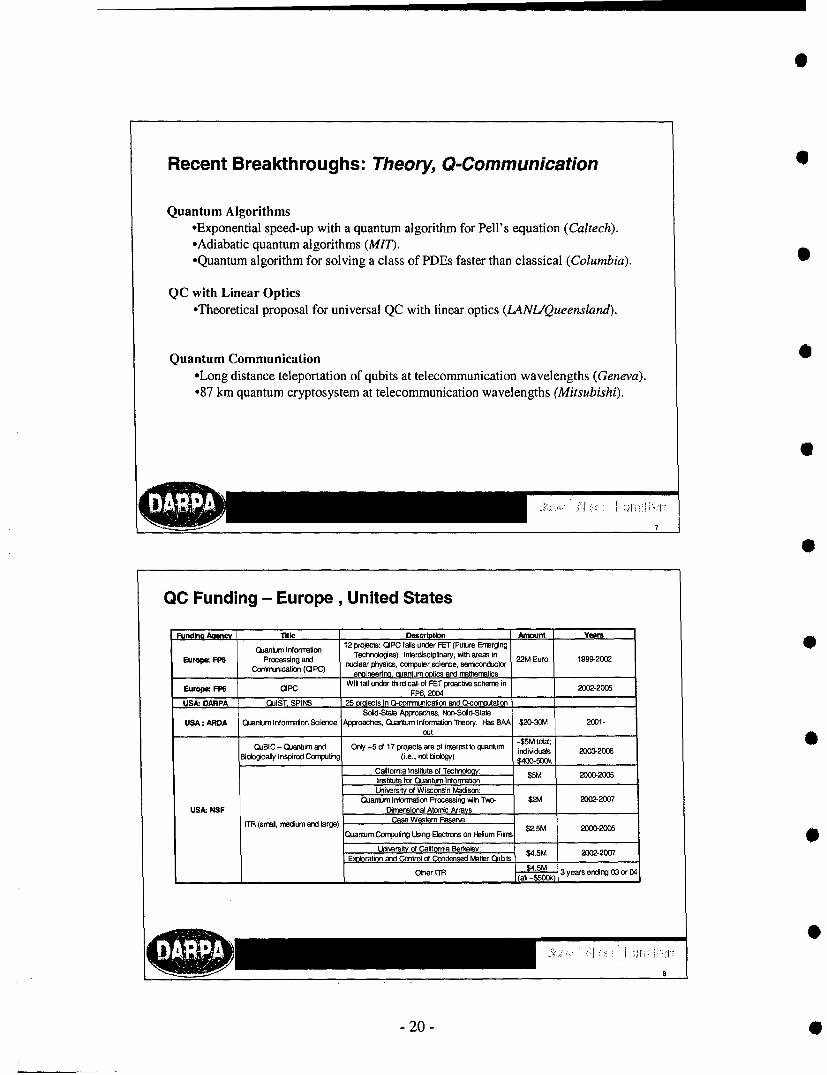
Recent Breakthroughs: Theory, 0-Communication
Quantum Algorithms*Exponential speed-up with a quantum algorithm for Pell's equation (Ca itech).'Adiabatic quantum algorithms (MIT).-Quantum algorithm for solving a class of PDEs faster than classical (Columbia).
QC with Linear Optics'Theoretical proposal for universal QC with linear optics (LANlJQueenslandj.
Quantum Communication0'Long distance teleportation of qubits at telecommunication wavelengths (Geneva).'87 km quantum cryptosystem at telecommunication wavelengths (Mitsubishi).
7
0
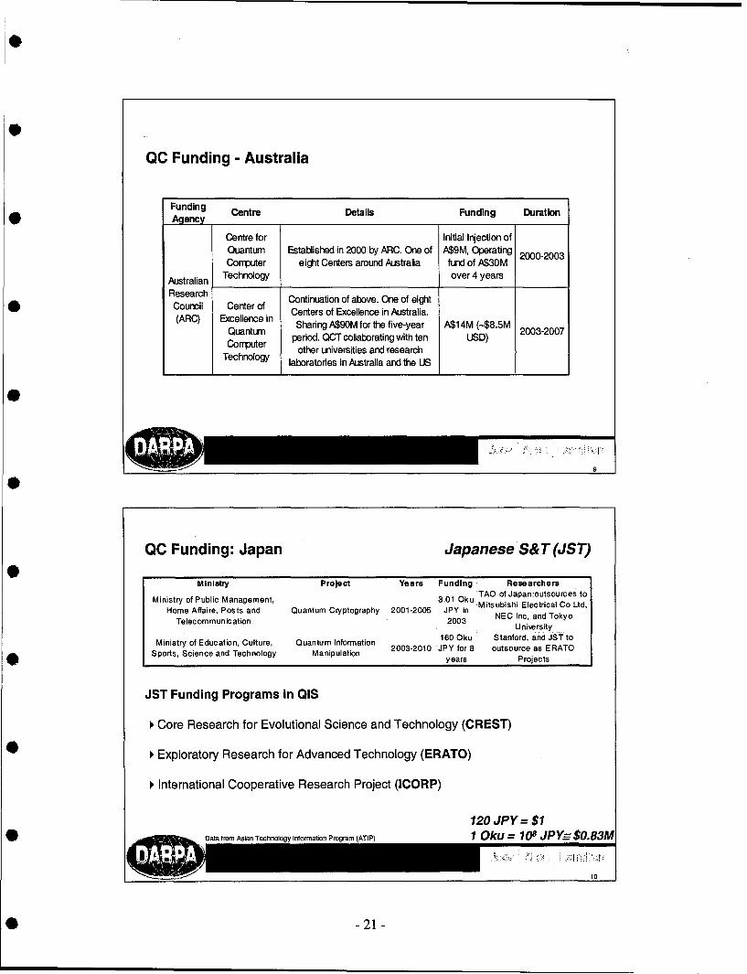
QC Funding - Europe, United States
Fundh¶ gec TItle Description Amount Years12 projectsa OPC fails under PET (Future Emerging 0QuantnhimInforrmaton Techncio~es). Interdisnciplinary, Wth areas in
Euoe CFS Ponmcesing a(d nu)rclear physics, com-puter science, semconuckjcor 22M Euro 1999-2002Cornunictio (ClPC) erd neernra. oQu um ootics arnd mathermatics
Euroe FP6 0PCWill fall under Ithird call of FET preoaes schem~e in 2002-2005FP6,2004__
USA: DARPA QuIST. SPINS 25 projecsf in O-cormmnication and O-computijbon____Sdlid-Ststsa Approaches, Non-Solid-State
USA: ARDA QuantumInformation Scienice Approaches, Quantum Information Theory, f-tas EM $20-30tvM 2001-
OuSIC - Quantum and Only -5cof 17 projects are of irterest to cluantumn $5IV Itual0Biologically Inspired Comrputing (ieno oeg)ldh4duasf 2003-2006
Caiufornia Institute of Technrology! $5M X000-2005Institute for Quanetum nfltormationI
inhersitv of Wisconsin fWedsomQuantum I nformationa Processing vaBh Two- I $2M 2003-2007
USA. NSF Dimnsmional Atomic Arrays
ITR (srraI, nfedum and large) Case Western aesern$25e2:-20Qusntum Com~puting Lising Electrons on -Helium riln 05 00-
Uni'.ersity of Cslfornia Berkeley: $.M M2UEusilorat ion and Control of Condensed Matter Quibts
Otheir tM fal SM 3 years ending 03 or 04
-20-
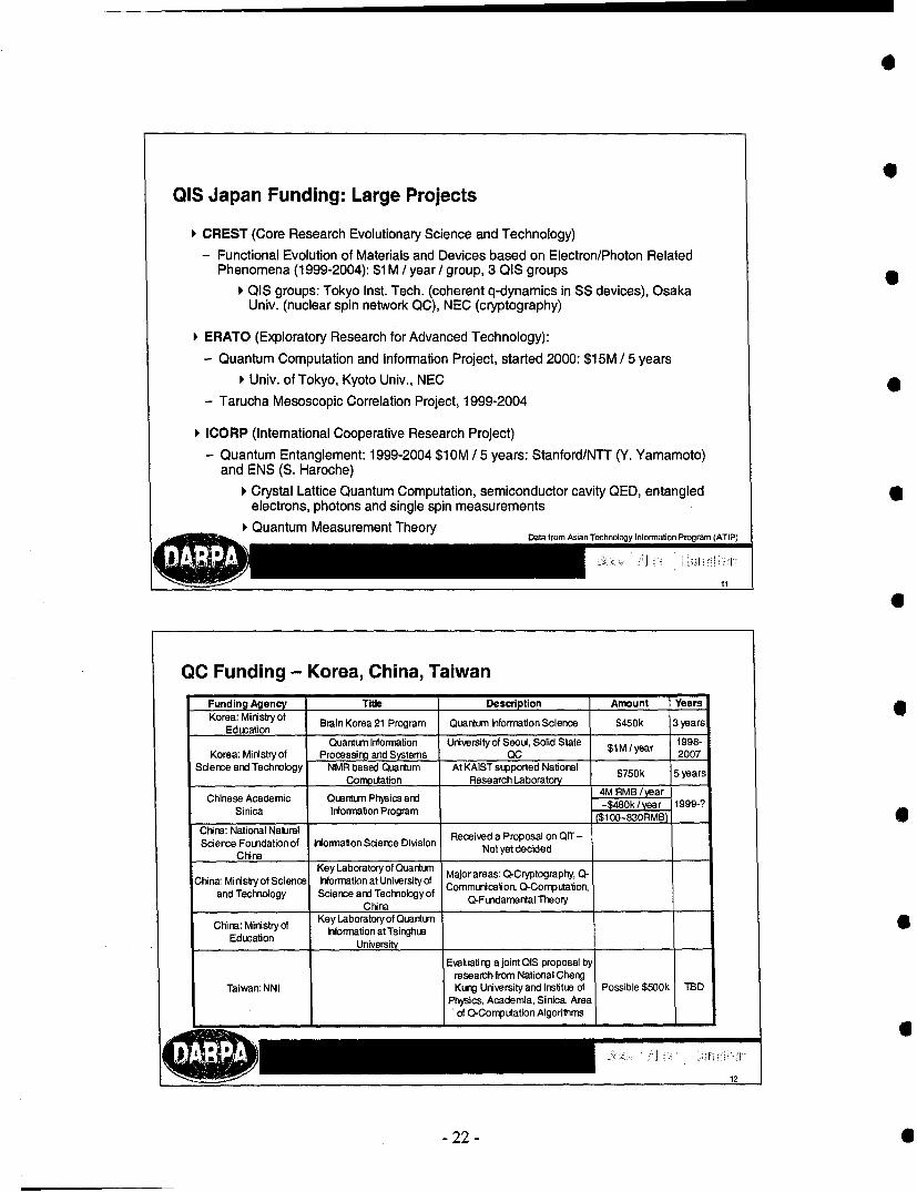
QC Funding - Australia
Funding Centre Details Funding Duration.Agency
Centre for Initial Injection ofQuantum Established in 2000 by ARC. One of A$9M, Operating 2000-2003Computer eight Centers around Australia fund of A$30M
Australian Technology over 4 years
Research Continuation of above. One of eight
Council Center of Centers of Excellence in Australia.(ARC) Excellence in Sharing A$90M for the five-year A$14M (-$8.5M 2003-2007
Quantum period. QCT collaborating with ten USD)Conputer other universities and research
Technology laboratories in Australia and the US
99QC Funding: Japan Japanese S& T (JS T)
Ministry Project Years :Funding Researchers
Ministry of Public Management, 3.01 Oku TAO ofJapan:outsources to.Mitsubishi Electrical Co Ltd,
Home Affaire, Posts and Quantum Cryptography 2001-2005 JPY inECctian Tokyo
Telecommunication 2003Unixersity
Ministry of Education, Culture, Quantum Information 160 Oku Stanford, and JST to
Sports, Science and Technology Manipulation 2003-2010 JPY for 8 outsource as ERATOyears Projects
JST Funding Programs in QIS
I, Core Research for Evolutional Science and Technology (CREST)
i Exploratory Research for Advanced Technology (ERATO)
ii International Cooperative Research Project (ICORP)
120 JPY = $1cats fronm Asian Technology Information Program (ATIP) 1 Oku 108 JPY $0.83M
* -21-
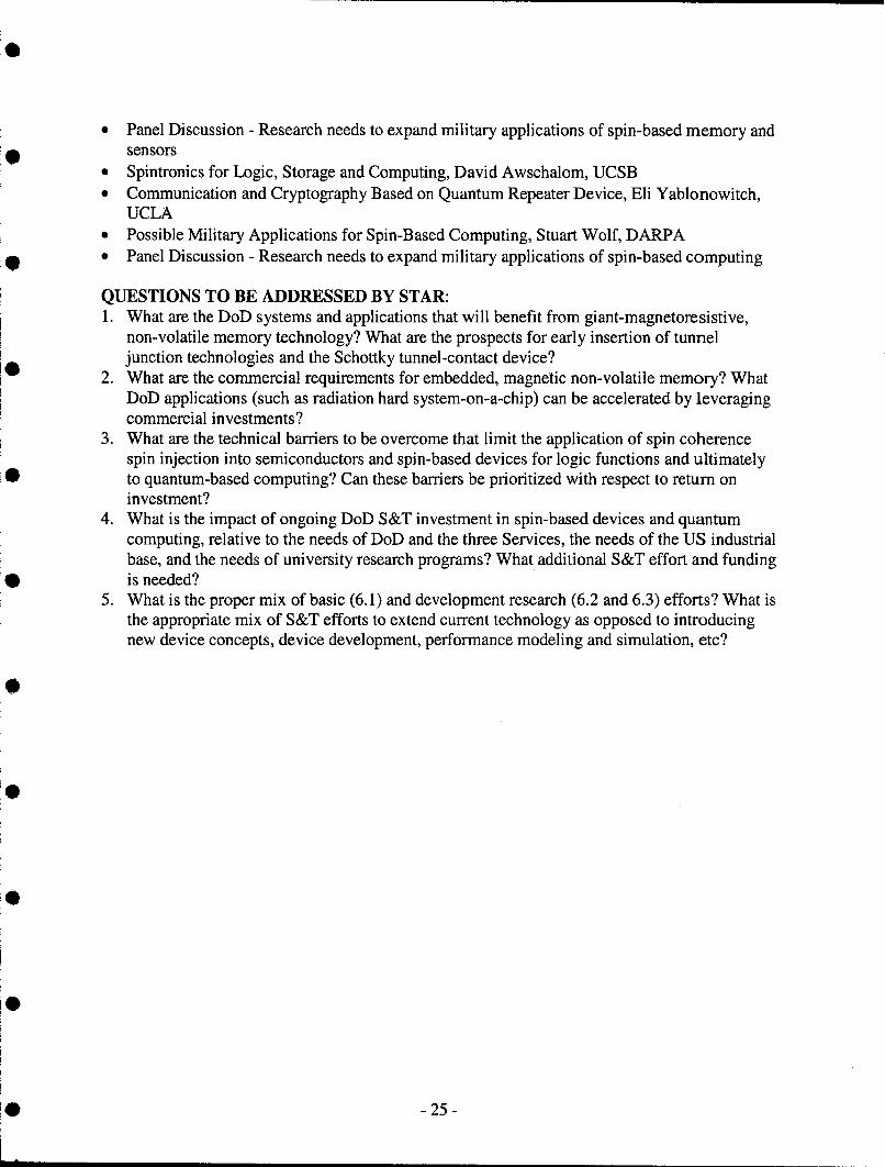
QIS Japan Funding: Large Projects
i0 CREST (Core Research Evolutionary Science and Technology)- Functional Evolution of Materials and Devices based on Electron/Photon Related
Phenomena (11999-2004): $1 M / year / group, 3 015 groups0 O15 groups: Tokyo Inst. Tech. (coherent q-dynamics in SS devices), Osaka
Univ. (nuclear spin network QC), NEC (cryptography)
il ERATO (Exploratory Research for Advanced Technology):- Quantum Computation and Information Project, started 2000: $15M / 5 years
ý Univ. of Tokyo, Kyoto Univ., NEC- Tarucha Mesoscopic Correlation Project, 1999-2004
il ICORP (International Cooperative Research Project)-Quantum Entanglement: 1999-2004 $1 OM / 5 years: Stanford/Nfl (Y. Yamamoto)
and ENS (S. Haroche)iý Crystal Lattice Quantum Computation, semiconductor cavity QED, entangled
electrons, photons and single spin measurementsý Quantum Measurement Theory Data from Asian Technology Information Program (ATIP)
OC Funding -Korea, China, TaiwanFunding Agency Title Description Amount YearsKorea: Ministry of Brain Korea 21 Program Ouatuninttformration Science $450k 3 years
EducationQuantumn Information University of Seoul, Solid State $M/ year 1998-
Korea: Ministry of Processing and Systems 00 2007Science and Technology NMR based Quantum At KAIST supported National $750k 5 years
Compqutation Research Laboratory ______
Chinese Acadermic Quanturn Physics andi I 480k ar 1999-?Sinica informaltion Program ______________ O3OM) __
China: National Natural Received a Proposal on 0fl -Science Foundation of Iriformation Science Division Not yet decided
ChnraKey Laboratory of Quarttum Major areas: 0-Cryptography, 0-
China: Ministry of Science kIformation at University of Commun~ication, Ct-Corrputation,and Tech-nology Science and Tecfhnology of 0-Funamental Theory
_______________~China_______ ____ _____
China: Ministry of Key Laboratory of QuantumnEducation Iformation at TsinghuaEductionUniversity
Evalujating a joint 0is proposal byresearch from National Cheng
Taiwart NNI Kung University and Iretitie, of Possible $500k TBDPhysics, Academia, Sinica. Area
'of Q-Cornputation Algorith~ms
12
-22-6

APPENDIX BTerms of Reference
DEPARTMENT OF DEFENSEADVISORY GROUP ON ELECTRON DEVICES (AGED)
* •WORKING GROUP B (Microelectronics)
SPECIAL TECHNOLOGY AREA REVIEWON
SPINTRONICS
TERMS OF REFERENCE
0 STAR ORGANIZERS:
Les Palkuti, DTRAStuart Wolf, DARPA
LENGTH: 1 day including discussion
VENUE: Fess Parker's DoubleTree Resort, Santa Barbara, CA
TIME: 19 March 2003
9 WHY TOPIC IS APPROPRIATE FOR AN AGED STAR:Spintronics (electronics based on the spin degree of freedom of the electron) is of great currentinterest and has the potential to revolutionize current charge based electronics. For example,giant magnetoresistive (GMR)-based non-volatile memory has the potential to replace Flash andDRAM. It is timely now to provide AGED and OSD with an up to date assessment of the
* military applications in this field.
OBJECTIVES:1. Evaluate the present status and progress in spin-based nonvolatile memory applications.2. Determine the military applications of this disruptive memory technology particularly as it
* relates applying the technology in space-based applications3. Review the potential for magnetic quantum-based logic and computing.4. Identify current technical barriers and impediments; and possible breakthroughs in quantum
spin-based computing technologies for future military system applications.5. Develop additional science and technology efforts to expand applications to DoD systems.
-23-

BACKGROUND:Until very recently, the spin of the electron was ignored in mainstream charge-based electronics.A new electronics technology based on the spin transport of the electron or spintronics hasrecently emerged, where it is not the electron charge but the electron spin that carriesinformation. Spin-based electronics offers remarkable opportunities for a new generation ofdevices combining standard microelectronics with spin-dependent effects that arise from theinteractions between electron spin, magnetic field and the magnetic properties of the material.An important spintronic device is the non-volatile memory based on the giant magnetoresistiveeffect. Within the next two years several companies including Motorola and IBM will introducethese magnetic non-volatile random access memories using the magnetic tunnel junction devices.This memory has significant military potential by replacing much of the existing semiconductormemories including Flash and DRAM and embedded GMR devices form the memory elementsin robust system-on-a-chip technology. Recent discoveries about induced spin coherence and 6spin injection into semiconductors have opened up even more possibilities for revolutionarydevices that can supplement or even supplant charge based semiconductor electronics for logicoperations. The prospects of developing a whole new computing infrastructure based on thequantum mechanical nature of electron or nuclear spin have emerged in recent years and thereare several large efforts that are trying to fabricate and understand the properties and limitationof spin based quantum bits. (For additional background see S. A. Wolf, D. D. Awschalom, R. A.Buhrman, J. Daughton, S. von Molnar, M. Roukes, A. Y. Chtchelkanova, D. M. Treger, Science,Vol 294, Nov 2001, pp 1488-1495; or Zorpette, Glenn, "The Quest for the Spin Transistor",IEEE Spectrum, Dec 2001, pp 30-35 - articles attached)
STAR OVERVIEW: •
Nonvolatile MemoryThese applications talks will provide in depth reviews of the major efforts to develop magneticrandom access memory (MRAM) based the magnetic tunnel junction devices integrated withCMOS. The first MRAM products are expected within the next two years. In addition, amagnetic Schottky tunnel contact device and process will be explored that has the potential for a100-fold increase in memory density.
Spin-Based Quantum ComputingThe next series of talks will focus on the development of a host of new technologies that rely onthe controllable interactions of coherent spins with ferromagnetic materials to produce quantumlogic operations. Recent advances in spin transport, spin injection and coherent spin behaviorhave enhanced the prospects for novel new devices for logic that may be faster and lower powerthan just charge based electronics. These talks will describe how spin is the perfect quantum bitor qubit that will make it possible for quantum computation. DoD applications for thistechnology will be addressed in detail.
Agenda0 GMR MRAM with Current-in-Plane Magnetic Devices, Romney Katti, Honeywell* Tunnel Junction MRAM, Speaker Saied Tehrani, Motorola0 GMR Sensors with Spin-Dependent Tunneling Technology, Jim Daughton, NVE9 Magnetic Tunnel Junction MRAM, Jim Gallagher, IBM
-24- -
"* Panel Discussion - Research needs to expand military applications of spin-based memory andsensors
"* Spintronics for Logic, Storage and Computing, David Awschalom, UCSB"* Communication and Cryptography Based on Quantum Repeater Device, Eli Yablonowitch,
UCLA"* Possible Military Applications for Spin-Based Computing, Stuart Wolf, DARPA* Panel Discussion - Research needs to expand military applications of spin-based computing
QUESTIONS TO BE ADDRESSED BY STAR:1. What are the DoD systems and applications that will benefit from giant-magnetoresistive,
non-volatile memory technology? What are the prospects for early insertion of tunneljunction technologies and the Schottky tunnel-contact device?
2. What are the commercial requirements for embedded, magnetic non-volatile memory? WhatDoD applications (such as radiation hard system-on-a-chip) can be accelerated by leveragingcommercial investments?
3. What are the technical barriers to be overcome that limit the application of spin coherencespin injection into semiconductors and spin-based devices for logic functions and ultimatelyto quantum-based computing? Can these barriers be prioritized with respect to return oninvestment?
4. What is the impact of ongoing DoD S&T investment in spin-based devices and quantumcomputing, relative to the needs of DoD and the three Services, the needs of the US industrialbase, and the needs of university research programs? What additional S&T effort and fundingis needed?
5. What is the proper mix of basic (6.1) and development research (6.2 and 6.3) efforts? What isthe appropriate mix of S&T efforts to extend current technology as opposed to introducingnew device concepts, device development, performance modeling and simulation, etc?
-25-

, , , I I I I I I I I I I I I
6
THIS PAGE INTENTIONALLY LEFT BLANKa
J6
tr4
I6
- 26- -
APPENDIX C* Agenda
DEPARTMENT OF DEFENSEADVISORY GROUP ON ELECTRON DEVICES (AGED)
* WORKING GROUP B (MICROELECTRONICS)
SPECIAL TECHNOLOGY AREA REVIEWon
SPINTRONICS
Wednesday, March 19, 2003
0730-0830 Continental Breakfast and Registration
0830-0840 Introduction
0840-0920 GMR MRAM with Current-in-Plane Magnetic Devices Romney Katti, Honeywell
0920-1000 Tunnel Junction MRAM Saied Tehrani, Motorola1000-1040 GMR Memory and Sensors with Spin-Dependent Jim Daughton, NVE
Tunneling Technology
1040-1100 Break
1100-1130 Magnetic Tunnel Junction MRAM Bill Gallagher, IBM
1130-1200 SpinRAM -All metal, based on GMR Richard Spitzer, IME (integratedMagnetoelectronics)
1200-1230 Research needs to expand military applications of Panel Discussionspin-based memory and sensors
1230-1330 Lunch
1330-1420 Spintronics for Logic, Storage and Computing David Awschalom, UCSB
1420-1510 Communication and Cryptography Based on Eli Yablonovitch, UCLAQuantum Repeater Device
1510-1545 Break
1545-1635 Possible Military Applications for Spin-Based Stuart Wolf, UVAComputing
1635-1650 Quantum Information Science Landscape Tatjana Curcic, UVA
1650-1715 Research Needs to Expand Military Applications of Panel DiscussionSpin-Based Computing
Meeting Adjourns
-27-
THIS PAGE INTENTIONALLY LEFT BLANK
ta
i6
S- 28- -

ACRONYMS
AGED Advisory Group on Electron Devices
AMR Anisotropic Magnetoresistance
CMOS Complementary Metal Oxide Semiconductor
CMR Colossal Magnetoresistance
DARPA Defense Advanced Research Projects Agency
DoD Department of Defense
4 DRAM Dynamic Random Access Memory
GMR Giant Magneto Resistive
MTJ Magnetic Tunnel Junction
MRAM Magnetic Random Access Memory
S&T Science and Technology
SOI Silicon on Insulator
SRAM Static Random Access Memory
STAR Special Technology Area Review
S&T Science and Technology
-29-


![Promises, Promises [Score]](https://img.dokumen.tips/doc/110x75/55cf922f550346f57b946648/promises-promises-score.jpg)