Embed Size (px)
Citation preview
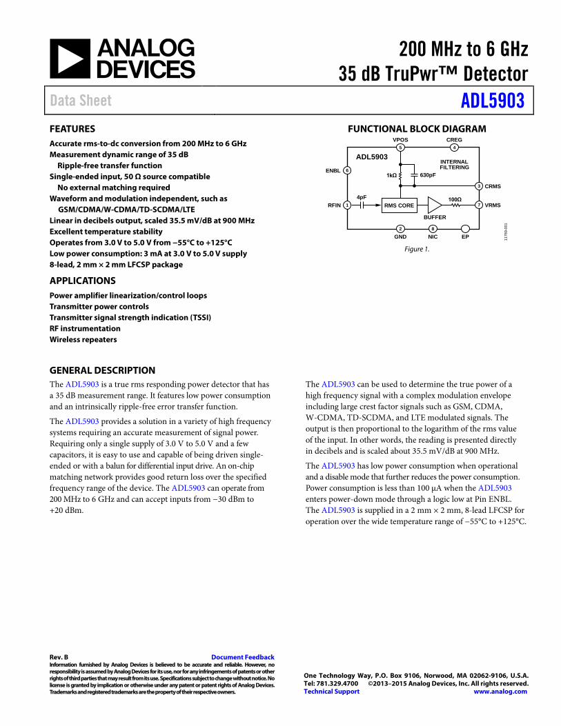
200 MHz to 6 GHz 35 dB TruPwr™ Detector
Data Sheet ADL5903
Rev. B Document Feedback Information furnished by Analog Devices is believed to be accurate and reliable. However, no responsibility is assumed by Analog Devices for its use, nor for any infringements of patents or other rights of third parties that may result from its use. Specifications subject to change without notice. No license is granted by implication or otherwise under any patent or patent rights of Analog Devices. Trademarks and registered trademarks are the property of their respective owners.
One Technology Way, P.O. Box 9106, Norwood, MA 02062-9106, U.S.A. Tel: 781.329.4700 ©2013–2015 Analog Devices, Inc. All rights reserved. Technical Support www.analog.com
FEATURES Accurate rms-to-dc conversion from 200 MHz to 6 GHz Measurement dynamic range of 35 dB
Ripple-free transfer function Single-ended input, 50 Ω source compatible
No external matching required Waveform and modulation independent, such as
GSM/CDMA/W-CDMA/TD-SCDMA/LTE Linear in decibels output, scaled 35.5 mV/dB at 900 MHz Excellent temperature stability Operates from 3.0 V to 5.0 V from −55°C to +125°C Low power consumption: 3 mA at 3.0 V to 5.0 V supply 8-lead, 2 mm × 2 mm LFCSP package
APPLICATIONS Power amplifier linearization/control loops Transmitter power controls Transmitter signal strength indication (TSSI) RF instrumentation Wireless repeaters
FUNCTIONAL BLOCK DIAGRAM
Figure 1.
GENERAL DESCRIPTION The ADL5903 is a true rms responding power detector that has a 35 dB measurement range. It features low power consumption and an intrinsically ripple-free error transfer function.
The ADL5903 provides a solution in a variety of high frequency systems requiring an accurate measurement of signal power. Requiring only a single supply of 3.0 V to 5.0 V and a few capacitors, it is easy to use and capable of being driven single-ended or with a balun for differential input drive. An on-chip matching network provides good return loss over the specified frequency range of the device. The ADL5903 can operate from 200 MHz to 6 GHz and can accept inputs from −30 dBm to +20 dBm.
The ADL5903 can be used to determine the true power of a high frequency signal with a complex modulation envelope including large crest factor signals such as GSM, CDMA, W-CDMA, TD-SCDMA, and LTE modulated signals. The output is then proportional to the logarithm of the rms value of the input. In other words, the reading is presented directly in decibels and is scaled about 35.5 mV/dB at 900 MHz.
The ADL5903 has low power consumption when operational and a disable mode that further reduces the power consumption. Power consumption is less than 100 µA when the ADL5903 enters power-down mode through a logic low at Pin ENBL. The ADL5903 is supplied in a 2 mm × 2 mm, 8-lead LFCSP for operation over the wide temperature range of −55°C to +125°C.
1176
9-00
1
5
1
6
ADL5903
RFIN
ENBL
RMS CORE
INTERNALFILTERING
BUFFER
630pF1kΩ
100Ω4pF
VPOS
2
GND8
NIC EP
4CREG
3 CRMS
7 VRMS
ADL5903 Data Sheet
Rev. B | Page 2 of 20
TABLE OF CONTENTS Features .............................................................................................. 1 Applications ....................................................................................... 1 Functional Block Diagram .............................................................. 1 General Description ......................................................................... 1 Revision History ............................................................................... 2 Specifications ..................................................................................... 3 Absolute Maximum Ratings ............................................................ 6
ESD Caution .................................................................................. 6 Pin Configuration and Function Descriptions ............................. 7 Typical Performance Characteristics ............................................. 8
Measurement Setups ...................................................................... 14 Theory of Operation ...................................................................... 15
RF Input Interface ...................................................................... 15 Basic Connections ...................................................................... 15 Choosing a Value for CRMS ......................................................... 16 Device Calibration and Error Calculation .............................. 17
Evaluation Board Schematic and Configuration Options ........ 19 Outline Dimensions ....................................................................... 20
Ordering Guide .......................................................................... 20
REVISION HISTORY 5/15—Rev. A to Rev. B
Changes to Figure 49 ...................................................................... 19
2/15—Rev. 0 to Rev. A
Added ADL5903ACPZN Operating Temperature Range of −40°C to +85°C; Table 2 .................................................................. 6 Changes to Ordering Guide .......................................................... 20
10/13—Revision 0: Initial Version

Data Sheet ADL5903
Rev. B | Page 3 of 20
SPECIFICATIONS VPOS = 5.0 V, TA = 25°C, ZO = 50 Ω, Capacitor CRMS = 10 nF, unless otherwise noted.
Table 1. Parameter Test Conditions/Comments Min Typ Max Unit OVERALL FUNCTION
Frequency Range 200 to 6000 MHz RF INPUT INTERFACE Pin RFIN
Nominal Input Impedance1 Single-ended drive 50 Ω OUTPUT INTERFACE Pin VRMS
DC Output Resistance 100 Ω Rise Time PIN = off to 0 dBm, 10% to 90%, CRMS = 10 nF 3.5 µs PIN = off to 0 dBm, 10% to 90%, CRMS = 100 nF 34 µs Fall Time PIN = 0 dBm to off, 90% to 10%, CRMS = 10 nF 32 µs PIN = 0 dBm to off, 90% to 10%, CRMS = 100 nF 330 µs
f = 300 MHz ±1.0 dB Dynamic Range Continuous wave (CW) input, TA = 25°C, VPOS = 5.0 V 37 dB CW input, TA = 25°C, VPOS = 3.0 V 34 dB Maximum Input Level, ±1.0 dB Three-point calibration at −16 dBm, −4 dBm, and +12 dBm 13 dBm Minimum Input Level, ±1.0 dB Three-point calibration at −16 dBm, −4 dBm, and +12 dBm −24 dBm Deviation vs. Temperature Deviation from output at 25°C
−40°C < TA < +85°C; PIN = 10 dBm −0.2/+0.032 dB −55°C < TA < +125°C; PIN = 10 dBm −0.25/+0.052 dB
−40°C < TA < +85°C; PIN = −10 dBm −0.2/+0.152 dB −55°C < TA < +125°C; PIN = −10 dBm −0.25/+0.22 dB Logarithmic Slope Calibration at −16 dBm and +4 dBm 36.3 mV/dB Logarithmic Intercept Calibration at −16 dBm and +4 dBm (X-intercept) −39 dBm
f = 700 MHz ±1.0 dB Dynamic Range CW input, TA = 25°C, VPOS = 5.0 V 37 dB CW input, TA = 25°C, VPOS = 3.0 V 34 dB Maximum Input Level, ±1.0 dB Three-point calibration at −16 dBm, −3 dBm, and +13 dBm 14 dBm Minimum Input Level, ±1.0 dB Three-point calibration at −16 dBm, −3 dBm, and +13 dBm −23 dBm Deviation vs. Temperature Deviation from output at 25°C
−40°C < TA < +85°C; PIN = 10 dBm −0.13 dB −55°C < TA < +125°C; PIN = 10 dBm −0.16 dB −40°C < TA < +85°C; PIN = −10 dBm −0.15/+0.12 dB −55°C < TA < +125°C; PIN = −10 dBm −0.2/+0.22 dB
Logarithmic Slope Calibration at −16 dBm and +4 dBm 36.4 mV/dB Logarithmic Intercept Calibration at −16 dBm and +4 dBm (X-intercept) −38 dBm
f = 900 MHz ±1.0 dB Dynamic Range CW input, TA = 25°C, VPOS = 5.0 V 37 dB CW input, TA = 25°C, VPOS = 3.0 V 33 dB Maximum Input Level, ±1.0 dB Three-point calibration at −16 dBm, −3 dBm, and +13 dBm 14 dBm Minimum Input Level, ±1.0 dB Three-point calibration at −16 dBm, −3 dBm, and +13 dBm −23 dBm Deviation vs. Temperature Deviation from output at 25°C −40°C < TA < +85°C; PIN = 10 dBm −0.12 dB −55°C < TA < +125°C; PIN = 10 dBm −0.15/+0.022 dB −40°C < TA < +85°C; PIN = −10 dBm −0.1/+0.022 dB −55°C < TA < +125°C; PIN = −10 dBm −0.1/+0.12 dB Logarithmic Slope Calibration at −16 dBm and +4 dBm 35.5 mV/dB Logarithmic Intercept Calibration at −16 dBm and +4 dBm (X-intercept) −38 dBm

ADL5903 Data Sheet
Rev. B | Page 4 of 20
Parameter Test Conditions/Comments Min Typ Max Unit f = 1900 MHz
±1.0 dB Dynamic Range CW input, TA = 25°C, VPOS = 5.0 V 37 dB CW input, TA = 25°C, VPOS = 3.0 V 33 dB Maximum Input Level, ±1.0 dB Three-point calibration at −15 dBm, −3 dBm, and +13 dBm 15 dBm Minimum Input Level, ±1.0 dB Three-point calibration at −15 dBm, −3 dBm, and +13 dBm −22 dBm Deviation vs. Temperature Deviation from output at 25°C
−40°C < TA < +85°C; PIN = 10 dBm −0.15 dB −55°C < TA < +125°C; PIN = 10 dBm −0.15 dB −40°C < TA < +85°C; PIN = −10 dBm −0.3/+0.22 dB −55°C < TA < +125°C; PIN = −10 dBm −0.35/+0.252 dB
Logarithmic Slope Calibration at −16 dBm and +4 dBm 37.2 mV/dB Logarithmic Intercept Calibration at −16 dBm and +4 dBm (X-intercept) −35.5 dBm
f = 2140 MHz ±1.0 dB Dynamic Range CW input, TA = 25°C, VPOS = 5.0 V 35 dB CW input, TA = 25°C, VPOS = 3.0 V 32 dB Maximum Input Level, ±1.0 dB Three-point calibration at −15 dBm, −3 dBm, and +13 dBm 15 dBm Minimum Input Level, ±1.0 dB Three-point calibration at −15 dBm, −3 dBm, and +13 dBm −20 dBm Deviation vs. Temperature Deviation from output at 25°C −40°C < TA < +85°C; PIN = 10 dBm −0.2 dB −55°C < TA < +125°C; PIN = 10 dBm −0.2 dB −40°C < TA < +85°C; PIN = −10 dBm −0.4/+0.22 dB −55°C < TA < +125°C; PIN = −10 dBm −0.5/+0.32 dB Logarithmic Slope Calibration at −16 dBm and +4 dBm 37.4 mV/dB Logarithmic Intercept Calibration at −16 dBm and +4 dBm (X-intercept) −35 dBm
f = 2600 MHz ±1.0 dB Dynamic Range CW input, TA = 25°C, VPOS = 5.0 V 34 dB CW input, TA = 25°C, VPOS = 3.0 V 32 dB Maximum Input Level, ±1.0 dB Three-point calibration at −14 dBm, −2 dBm, and +14 dBm 15 dBm Minimum Input Level, ±1.0 dB Three-point calibration at −14 dBm, −2 dBm, and +14 dBm −19 dBm Deviation vs. Temperature Deviation from output at 25°C −40°C < TA < +85°C; PIN = 10 dBm −0.2 dB −55°C < TA < +125°C; PIN = 10 dBm −0.25 dB −40°C < TA < +85°C; PIN = −10 dBm −0.5/+0.22 dB −55°C < TA < +125°C; PIN = −10 dBm −0.6/+0.32 dB Logarithmic Slope Calibration at −16 dBm and +4 dBm 37.7 mV/dB Logarithmic Intercept Calibration at −16 dBm and +4 dBm (X-intercept) −34 dBm
f = 3500 MHz ±1.0 dB Dynamic Range CW input, TA = 25°C, VPOS = 5.0 V 33 dB CW input, TA = 25°C, VPOS = 3.0 V 31 dB Maximum Input Level, ±1.0 dB Three-point calibration at −12 dBm, 0 dBm, and +14 dBm 16 dBm Minimum Input Level, ±1.0 dB Three-point calibration at −12 dBm, 0 dBm, and +14 dBm −17 dBm Deviation vs. Temperature Deviation from output at 25°C −40°C < TA < +85°C; PIN = 10 dBm −0.2 dB −55°C < TA < +125°C; PIN = 10 dBm −0.25 dB −40°C < TA < +85°C; PIN = −10 dBm −0.6/+0.32 dB −55°C < TA < +125°C; PIN = −10 dBm −0.75/+0.42 dB Logarithmic Slope Calibration at −12 dBm and +8 dBm 39 mV/dB Logarithmic Intercept Calibration at −12 dBm and +8 dBm (X-intercept) −31.5 dBm

Data Sheet ADL5903
Rev. B | Page 5 of 20
Parameter Test Conditions/Comments Min Typ Max Unit f = 5800 MHz
±1.0 dB Dynamic Range CW input, TA = 25°C, VPOS = 5.0 V 35 dB CW input, TA = 25°C, VPOS = 3.0 V 32 dB Maximum Input Level, ±1.0 dB Three-point calibration at −12 dBm, −2 dBm, and +12 dBm 19 dBm Minimum Input Level, ±1.0 dB Three-point calibration at −12 dBm, −2 dBm, and +12 dBm −16 dBm Deviation vs. Temperature Deviation from output at 25°C −40°C < TA < +85°C; PIN = 10 dBm −0.6/+0.32 dB −55°C < TA < +125°C; PIN = 10 dBm −0.7/+0.42 dB −40°C < TA < +85°C; PIN = −10 dBm −1.1/+0.72 dB −55°C < TA < +125°C; PIN = −10 dBm −1.4/+1.12 dB Logarithmic Slope Calibration at −12 dBm and +8 dBm 40 mV/dB Logarithmic Intercept Calibration at −12 dBm and +8 dBm (X-intercept) −27 dBm
POWER-DOWN INTERFACE Pin ENBL Voltage Level to Enable 2 VPOS V Voltage Level to Disable 0 0.6 V Input Bias Current VENBL = 2.2 V <20 nA
POWER SUPPLY INTERFACE Pin VPOS Supply Voltage 3.0 5.25 V Quiescent Current TA = 25°C, no signal at RFIN, VPOS = 5.0 V 3 mA TA = 125°C, no signal at RFIN, VPOS = 5.0 V 3.6 mA Power-Down Current ENBL input low condition <100 µA
1 Refer to Figure 12, input return loss, S11 (dB). 2 The slash indicates a range. For example, −0.2/+0.03 means −0.2 to +0.03.

ADL5903 Data Sheet
Rev. B | Page 6 of 20
ABSOLUTE MAXIMUM RATINGS Table 2. Parameter Rating Supply Voltage, VPOS 5.5 V Input Average RF Power1, 2 20 dBm
Equivalent Voltage, Sine Wave Input 3.16 V peak Internal Power Dissipation 200 mW θJC
3 3.95°C/W θJA
3 78.5°C/W Maximum Junction Temperature 150°C Operating Temperature Range (ADL5903ACPZN)
−40°C to +85°C
Operating Temperature Range (ADL5903SCPZN)
−55°C to +125°C
Storage Temperature Range −65°C to +150°C Lead Temperature (Soldering, 60 sec) 300°C 1 This is for long durations. Excursions above this level, with durations much
less than 1 second, are possible without damage. 2 Driven from a 50 Ω source. 3 No airflow with the exposed pad soldered to a 4-layer JEDEC board.
Stresses at or above those listed under Absolute Maximum Ratings may cause permanent damage to the product. This is a stress rating only; functional operation of the product at these or any other conditions above those indicated in the operational section of this specification is not implied. Operation beyond the maximum operating conditions for extended periods may affect product reliability.
ESD CAUTION

Data Sheet ADL5903
Rev. B | Page 7 of 20
PIN CONFIGURATION AND FUNCTION DESCRIPTIONS
Figure 2. Pin Configuration
Table 3. Pin Function Descriptions Pin No. Mnemonic Description 1 RFIN Signal Input. This pin is internally ac-coupled with a broadband matching network. See the RF Input Interface
section for broadband matching options. 2 GND Device Ground. Connect GND to system ground using a low impedance path. 3 CRMS RMS Averaging Pin. Connect a capacitor between the CREG and CRMS pins for rms averaging. See the
Choosing a Value for CRMS section for choosing the correct CRMS capacitor value. 4 CREG Bypass Capacitor Connection for On-Chip Regulator. Bypass this pin to ground using a capacitor and a series
resistor. See Basic Connections section for more information. 5 VPOS Supply Voltage. The operational range is 3.0 V to 5.25 V. 6 ENBL Enable. Connect the ENBL pin to a logic high (2 V to VPOS) to enable the device. Connect the ENBL pin to a
logic low (0 V to 0.6 V) to disable the device. 7 VRMS Signal Output. The output from the VRMS pin is proportional to the logarithm of the rms value at the input
level. 8 NIC No Internal Connection. Do not connect to this pin. This pin is not internally connected. 0 EP Exposed Pad. The exposed pad is internally connected to GND and requires a good thermal and electrical
connection to the ground of the printed circuit board (PCB).
1176
9-00
2
3CRMS
4CREG
1RFIN
2GND
6 ENBL
5 VPOS
8 NIC
7 VRMSADL5903TOP VIEW
(Not to Scale)
NOTES1. NIC = NO INTERNAL CONNECTION.2. THE EXPOSED PAD IS INTERNALLY CONNECTED TO GND
AND REQUIRES A GOOD THERMAL AND ELECTRICALCONNECTION TO THE GROUND OF THE PRINTEDCIRCUIT BOARD (PCB).

ADL5903 Data Sheet
Rev. B | Page 8 of 20
TYPICAL PERFORMANCE CHARACTERISTICS VPOS = 5.0 V, CRMS = 10 nF, TA = −55°C (light blue), TA = −40°C (blue), +25°C (green), +85°C (red), +125°C (orange) where appropriate. Input levels referred to 50 Ω source. Input RF signal is a sine wave (CW), unless otherwise indicated.
Figure 3. Typical VRMS vs. Input Level vs. Frequency
(300 MHz to 5.80 GHz) at 25°C
Figure 4. Error from CW Linear Reference vs. Input Level and Signal
Modulation (QPSK, 16 QAM, 64 QAM), Frequency = 900 MHz, CRMS = 1 µF
Figure 5. Error from CW Linear Reference vs. Input Level and Signal
Modulation (One-Carrier W-CDMA, Four-Carrier W-CDMA), Frequency = 2.14 GHz, CRMS = 1 µF
Figure 6. Typical VRMS vs. Frequency for Four Input Levels
Figure 7. Error from CW Linear Reference vs. Input Level and Signal
Modulation (QPSK, 16 QAM, 64 QAM), Frequency = 2.14 GHz, CRMS = 1 µF
Figure 8. Error from CW Linear Reference vs. Input Level and Signal
Modulation (LTE TM1 One-Carrier, 20 MHz), Frequency = 2.14 GHz, CRMS = 1 µF
20151050–5–10–15–20–25–30–35–40
2.0
1.8
1.6
1.4
1.2
1.0
0.8
0.6
0.4
0.2
0.0
PIN (dBm)
OU
TPU
T VO
LTA
GE
(V)
300MHz700MHz900MHz1.90GHz2.14GHz2.60GHz3.50GHz5.80GHz
1176
9-00
3
1176
9-00
4
1050–5–10–15–20–30
2.4
2.2
2.0
1.8
1.6
1.4
1.2
1.0
0.8
0.6
0.4
0.2
0
PIN (dBm)
OU
TPU
T VO
LTA
GE
(V)
CW16 QAM PEP = 6.34dB64 QAM PEP = 7.17dBQPSK PEP = 3.8dB
6
5
4
3
2
1
0
–1
–2
–3
–4
–5
–6
ERR
OR
(dB
)
CALIBRATION AT –16dBm, –3dBm, AND +8dBm
–25
1176
9-00
5
2.4
2.2
2.0
1.8
1.6
1.4
1.2
1.0
0.8
0.6
0.4
0.2
0
6
5
4
3
2
1
0
–1
–2
–3
–4
–5
–6
PIN (dBm)
OU
TPU
T VO
LTA
GE
(V)
ERR
OR
(dB
)
CW4-CARRIER W-CDMA PEP = 12.08dBm1-CARRIER W-CDMA PEP = 10.56dB
1050–5–10–15–20–25–30
CALIBRATION AT –15dBm, –3dBm, AND +8dBm
1G 6G100M
2.0
1.5
1.0
0.5
0
FREQUENCY (Hz)
OU
TPU
T VO
LTA
GE
(V)
–20dBm–10dBm0dBm10dBm
1176
9-00
6
1176
9-00
7
1050–5–10–15–20–25–30
2.4
2.2
2.0
1.8
1.6
1.4
1.2
1.0
0.8
0.6
0.4
0.2
0
PIN (dBm)
OU
TPU
T VO
LTA
GE
(V)
6
5
4
3
2
1
0
–1
–2
–3
–4
–5
–6
ERR
OR
(dB
)
CW16 QAM PEP = 6.34dB64 QAM PEP = 7.17dBQPSK PEP = 3.8dB
CALIBRATION AT –15dBm, –3dBm, AND +8dBm
1050–5–10–15–20–25–30
2.4
2.2
2.0
1.8
1.6
1.4
1.2
1.0
0.8
0.6
0.4
0.2
0
6
5
4
3
2
1
0
–1
–2
–3
–4
–5
–6
PIN (dBm)
OU
TPU
T VO
LTA
GE
(V)
ERR
OR
(dB
)CWLTE TM1 1-CARRIER 20MHz PEP = 11.58dB
1176
9-00
8
CALIBRATION AT –15dBm, –3dBm, AND +8dBm
Data Sheet ADL5903
Rev. B | Page 9 of 20
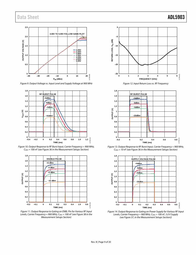
Figure 9. Output Voltage vs. Input Level and Supply Voltage at 900 MHz
Figure 10. Output Response to RF Burst Input, Carrier Frequency = 900 MHz,
CRMS = 100 nF (see Figure 36 in the Measurement Setups Section)
Figure 11. Output Response to Gating on ENBL Pin for Various RF Input Levels, Carrier Frequency = 900 MHz, CRMS = 100 nF (see Figure 38 in the
Measurement Setups Section)
Figure 12. Input Return Loss vs. RF Frequency
Figure 13. Output Response to RF Burst Input, Carrier Frequency = 900 MHz,
CRMS = 10 nF (see Figure 36 in the Measurement Setups Section)
Figure 14. Output Response to Gating on Power Supply for Various RF Input
Levels, Carrier Frequency = 900 MHz, CRMS = 100 nF, 5.0 V Supply (see Figure 37, in the Measurement Setups Section))
0
0.5
1.0
1.5
2.0
2.5
–40 –30 –20 –10 0 10 20
OU
TPU
T VO
LTA
GE
(V)
PIN (dBm)
3.00V3.40V3.80V4.00V4.25V4.50V5.00V
1176
9-00
9
4.00V TO 5.00V FOLLOW SAME PLOT
0
0.2
0.4
0.6
0.8
1.0
1.2
1.4
1.6
1.8
–0.4 –0.2 0 0.2 0.4 0.6 0.8 1.0 1.2
V OU
T (V
)
TIME (ms)
RF BURST PULSE
+5dBm
0dBm
–5dBm
–15dBm
1176
9-01
0
0
0.2
0.4
0.6
0.8
1.0
1.2
1.4
1.6
1.8
–0.2 –0.1 0 0.1 0.2 0.3 0.4 1.5 0.6
OU
TPU
T (V
)
TIME (ms) 1176
9-01
6
ENABLE PULSE
+5 dBm
0 dBm
–5 dBm
–15 dBm
–25
–20
–15
–10
–5
0
0 1 2 3 4 5 6
RET
UR
N L
OSS
, S11
(dB
)
FREQUENCY (GHz) 1176
9-01
2
0
0.2
0.4
0.6
0.8
1
1.2
1.4
1.6
1.8
–0.2 0 0.2 0.4 0.6 0.8
OU
TPU
T (V
)
TIME (ms)
+5dBm
0dBm
–5dBm
–15dBm
RF BURST PULSE
1176
9-01
1
0
0.2
0.4
0.6
0.8
1.0
1.2
1.4
1.6
1.8
–0.2 –0.1 0 0.1 0.2 0.3 0.4 0.5 0.6
OU
TPU
T (V
)
TIME (ms)
SUPPLY VOLTAGE PULSE
+5dBm
0dBm
–5dBm
–15dBm11
769-
015

ADL5903 Data Sheet
Rev. B | Page 10 of 20
Figure 15. VRMS and Log Conformance Error vs. Input Level and Temperature
at 300 MHz
Figure 16. VRMS and Log Conformance Error vs. Input Level and Temperature
at 700 MHz
Figure 17. VRMS and Log Conformance Error vs. Input Level and Temperature
at 900 MHz
Figure 18. Distribution of Log Conformance Error with Respect to Calibration
at 25°C vs. Input Level and Temperature at 300 MHz
Figure 19. Distribution of Log Conformance Error with Respect to Calibration
at 25°C vs. Input Level and Temperature at 700 MHz
Figure 20. Distribution of Log Conformance Error with Respect to Calibration
at 25°C vs. Input Level and Temperature at 900 MHz
20151050–5–10–15–20–25–30–35–40
2.4
2.2
2.0
1.8
1.6
1.4
1.2
1.0
0.8
0.6
0.4
0.2
0
6
5
4
3
2
1
0
–1
–2
–3
–4
–5
–6
PIN (dBm)
OU
TPU
T VO
LTA
GE
(V)
ERR
OR
(dB
)
–55°C–40°C+25°C+85°C+125°C
1176
9-01
7
CALIBRATION AT –16dBm, –4dBm, AND +12dBm
20151050–5–10–15–20–25–30–35–40
2.4
2.2
2.0
1.8
1.6
1.4
1.2
1.0
0.8
0.6
0.4
0.2
0
6
5
4
3
2
1
0
–1
–2
–3
–4
–5
–6
PIN (dBm)
OU
TPU
T VO
LTA
GE
(V)
ERR
OR
(dB
)
–55°C–40°C+25°C+85°C+125°C
1176
9-02
1
CALIBRATION AT –16dBm, –3dBm, AND +13dBm
20151050–5–10–15–20–25–30–35–40
2.4
2.2
2.0
1.8
1.6
1.4
1.2
1.0
0.8
0.6
0.4
0.2
0
6
5
4
3
2
1
0
–1
–2
–3
–4
–5
–6
PIN (dBm)
OU
TPU
T VO
LTA
GE
(V)
ERR
OR
(dB
)
–55°C–40°C+25°C+85°C+125°C
1176
9-02
2
CALIBRATION AT –16dBm, –3dBm, AND +13dBm
20151050–5–10–15–20–25–30–35–40
2.4
2.2
2.0
1.8
1.6
1.4
1.2
1.0
0.8
0.6
0.4
0.2
0
6
5
4
3
2
1
0
–1
–2
–3
–4
–5
–6
PIN (dBm)
OU
TPU
T VO
LTA
GE
(V)
ERR
OR
(dB
)
–55°C–40°C+25°C+85°C+125°C
1176
9-02
0
20151050–5–10–15–20–25–30–35–40
2.4
2.2
2.0
1.8
1.6
1.4
1.2
1.0
0.8
0.6
0.4
0.2
0
6
5
4
3
2
1
0
–1
–2
–3
–4
–5
–6
PIN (dBm)
OU
TPU
T VO
LTA
GE
(V)
ERR
OR
(dB
)11
769-
024
–55°C–40°C+25°C+85°C+125°C
2.4
2.2
2.0
1.8
1.6
1.4
1.2
1.0
0.8
0.6
0.4
0.2
0
6
5
4
3
2
1
0
–1
–2
–3
–4
–5
–6
OU
TPU
T VO
LTA
GE
(V)
ERR
OR
(dB
)
–55°C–40°C+25°C+85°C+125°C
20151050–5–10–15–20–25–30–35–40PIN (dBm) 11
769-
025

Data Sheet ADL5903
Rev. B | Page 11 of 20
Figure 21. VRMS and Log Conformance Error vs. Input Level and Temperature
at 1.9 GHz
Figure 22. VRMS and Log Conformance Error vs. Input Level and Temperature
at 2.14 GHz
Figure 23. VRMS and Log Conformance Error vs. Input Level and Temperature
at 2.6 GHz
Figure 24. Distribution of Log Conformance Error with Respect to Calibration
at 25°C vs. Input Level and Temperature at 1.9 GHz
Figure 25. Distribution of Log Conformance Error with Respect to Calibration
at 25°C vs. Input Level and Temperature at 2.14 GHz
Figure 26. Distribution of Log Conformance Error with Respect to Calibration
at 25°C vs. Input Level and Temperature at 2.6 GHz
20151050–5–10–15–20–25–30–35–40
2.4
2.2
2.0
1.8
1.6
1.4
1.2
1.0
0.8
0.6
0.4
0.2
0
6
5
4
3
2
1
0
–1
–2
–3
–4
–5
–6
PIN (dBm)
OU
TPU
T VO
LTA
GE
(V)
ERR
OR
(dB
)
–55°C–40°C+25°C+85°C+125°C
1176
9-02
3
CALIBRATION AT –15dBm, –3dBm, AND +13dBm
2.4
2.2
2.0
1.8
1.6
1.4
1.2
1.0
0.8
0.6
0.4
0.2
0
6
5
4
3
2
1
0
–1
–2
–3
–4
–5
–6
OU
TPU
T VO
LTA
GE
(V)
20151050–5–10–15–20–25–30–35–40PIN (dBm)
ERR
OR
(dB
)
–55°C–40°C+25°C+85°C+125°C
1176
9-02
7CALIBRATION AT –15dBm, –3dBm, AND +13dBm
2.4
2.2
2.0
1.8
1.6
1.4
1.2
1.0
0.8
0.6
0.4
0.2
0
6
5
4
3
2
1
0
–1
–2
–3
–4
–5
–6
OU
TPU
T VO
LTA
GE
(V)
20151050–5–10–15–20–25–30–35–40PIN (dBm)
ERR
OR
(dB
)
2015
–55°C–40°C+25°C+85°C+125°C
1176
9-02
8
CALIBRATION AT –14dBm, –2dBm, AND +14dBm
2.4
2.2
2.0
1.8
1.6
1.4
1.2
1.0
0.8
0.6
0.4
0.2
0
6
5
4
3
2
1
0
–1
–2
–3
–4
–5
–6
OU
TPU
T VO
LTA
GE
(V)
ERR
OR
(dB
)
20151050–5–10–15–20–25–30–35–40PIN (dBm) 11
769-
026
–55°C–40°C+25°C+85°C+125°C
2.4
2.2
2.0
1.8
1.6
1.4
1.2
1.0
0.8
0.6
0.4
0.2
0
6
5
4
3
2
1
0
–1
–2
–3
–4
–5
–6
OU
TPU
T VO
LTA
GE
(V)
ERR
OR
(dB
)
20151050–5–10–15–20–25–30–35–40PIN (dBm) 11
769-
030
–55°C–40°C+25°C+85°C+125°C
2.4
2.2
2.0
1.8
1.6
1.4
1.2
1.0
0.8
0.6
0.4
0.2
0
6
5
4
3
2
1
0
–1
–2
–3
–4
–5
–6
OU
TPU
T VO
LTA
GE
(V)
ERR
OR
(dB
)
–55°C–40°C+25°C+85°C+125°C
20151050–5–10–15–20–25–30–35–40PIN (dBm) 11
769-
031

ADL5903 Data Sheet
Rev. B | Page 12 of 20
Figure 27. VRMS and Log Conformance Error vs. Input Level and Temperature
at 3.5 GHz
Figure 28. VRMS and Log Conformance Error vs. Input Level and Temperature
at 5.8 GHz
Figure 29. Distribution of VRMS, PIN = 8 dBm, 900 MHz
Figure 30. Distribution of Log Conformance Error with Respect to Calibration
at 25°C vs. Input Level and Temperature at 3.5 GHz
Figure 31. Distribution of Log Conformance Error with Respect to Calibration
at 25°C vs. Input Level and Temperature at 5.8 GHz
Figure 32. Distribution of VRMS, PIN = −16 dBm, 900 MHz
2.4
2.2
2.0
1.8
1.6
1.4
1.2
1.0
0.8
0.6
0.4
0.2
0
6
5
4
3
2
1
0
–1
–2
–3
–4
–5
–6
OU
TPU
T VO
LTA
GE
(V)
20151050–5–10–15–20–25–30–35–40PIN (dBm)
ERR
OR
(dB
)
2015
–55°C–40°C+25°C+85°C+125°C
1176
9-02
9
CALIBRATION AT –12dBm, 0Bm, AND +14dBm
2.4
2.2
2.0
1.8
1.6
1.4
1.2
1.0
0.8
0.6
0.4
0.2
0
6
5
4
3
2
1
0
–1
–2
–3
–4
–5
–6
OU
TPU
T VO
LTA
GE
(V)
20151050–5–10–15–20–25–30–35–40PIN (dBm)
ERR
OR
(dB
)
–55°C–40°C+25°C+85°C+125°C
1176
9-03
3
CALIBRATION AT –12dBm, –2dBm, AND +12dBm
1.50 1.55 1.60 1.65 1.70 1.750
200
400
600
800
1000
1200
1400
VRMS (V)
CO
UN
T
1176
9-03
4
REPRESENTS MORETHAN 8000 PARTS
2.4
2.2
2.0
1.8
1.6
1.4
1.2
1.0
0.8
0.6
0.4
0.2
0
6
5
4
3
2
1
0
–1
–2
–3
–4
–5
–6
OU
TPU
T VO
LTA
GE
(V)
ERR
OR
(dB
)
–55°C–40°C+25°C+85°C+125°C
1176
9-03
2
20151050–5–10–15–20–25–30–35–40PIN (dBm)
2.4
2.2
2.0
1.8
1.6
1.4
1.2
1.0
0.8
0.6
0.4
0.2
0
6
5
4
3
2
1
0
–1
–2
–3
–4
–5
–6
OU
TPU
T VO
LTA
GE
(V)
ERR
OR
(dB
)
–55°C–40°C+25°C+85°C+125°C
1176
9-03
6
20151050–5–10–15–20–25–30–35–40PIN (dBm)
0.60 0.65 0.70 0.75 0.80 0.850
200
400
600
800
1000
1200
1400
VRMS (V)
CO
UN
T
1176
9-03
7
REPRESENTS MORETHAN 8000 PARTS

Data Sheet ADL5903
Rev. B | Page 13 of 20
Figure 33. Distribution of Intercept at 900 MHz
Figure 34. Supply Current vs. Input Level (at −55°C, −40°C, +25°C, +85°C, +125°C)
Figure 35. Distribution of Slope at 900 MHz
–44 –42 –40 –38 –36 –34 –320
200
400
600
800
1000
1200
1400
INTERCEPT (dBm)
CO
UN
T
1176
9-03
8
REPRESENTS MORETHAN 8000 PARTS
CALIBRATION BETWEEN–16dBm AND –4dBm
20100–10–20–30–40
30
25
20
15
10
5
0
PIN (dBm)
SUPP
LY C
UR
REN
T (m
A)
–55°C–40°C+25°C+85°C+125°C
1176
9-01
4
30 32 34 36 38 400
200
400
600
800
1000
1200
SLOPE (mV/dB)
CO
UN
T
1176
9-03
5
REPRESENTS MORETHAN 8000 PARTS
CALIBRATION BETWEEN–16dBm AND –4dBm
ADL5903 Data Sheet
Rev. B | Page 14 of 20
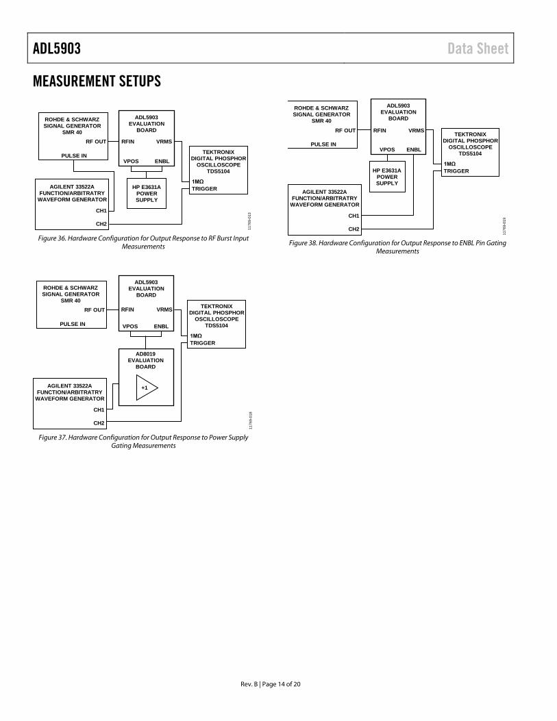
MEASUREMENT SETUPS
Figure 36. Hardware Configuration for Output Response to RF Burst Input
Measurements
Figure 37. Hardware Configuration for Output Response to Power Supply
Gating Measurements
Figure 38. Hardware Configuration for Output Response to ENBL Pin Gating
Measurements
ROHDE & SCHWARZSIGNAL GENERATOR
SMR 40
ADL5903EVALUATION
BOARD
PULSE IN
RF OUT RFIN
VPOS ENBL
1MΩTRIGGER
VRMS
HP E3631APOWERSUPPLY
AGILENT 33522AFUNCTION/ARBITRATRY
WAVEFORM GENERATOR
CH2
CH1
TEKTRONIXDIGITAL PHOSPHOR
OSCILLOSCOPETDS5104
1176
9-01
3
AD8019EVALUATION
BOARD
+1
1176
9-01
8
ROHDE & SCHWARZSIGNAL GENERATOR
SMR 40
ADL5903EVALUATION
BOARD
PULSE IN
RF OUT RFIN
1MΩTRIGGER
VRMS
AGILENT 33522AFUNCTION/ARBITRATRY
WAVEFORM GENERATOR
CH2
CH1
TEKTRONIXDIGITAL PHOSPHOR
OSCILLOSCOPETDS5104VPOS ENBL
1176
9-01
9
ROHDE & SCHWARZSIGNAL GENERATOR
SMR 40
ADL5903EVALUATION
BOARD
PULSE IN
RF OUT RFIN
VPOS ENBL
1MΩTRIGGER
VRMS
HP E3631APOWERSUPPLY
AGILENT 33522AFUNCTION/ARBITRATRY
WAVEFORM GENERATOR
CH2
CH1
TEKTRONIXDIGITAL PHOSPHOR
OSCILLOSCOPETDS5104

Data Sheet ADL5903
Rev. B | Page 15 of 20
THEORY OF OPERATION The ADL5903 is a true rms detector with a 35 dB measurement range at 2.14 GHz with useable range up to 6 GHz. It features no error ripple over its range, low temperature drift, and very low power consumption. Temperature stability of the rms output measurements provides ≤±0.5 dB error typical over the temperature range of −40°C to +85°C up to 3.5 GHz. The measurement output voltage scales linearly in decibels with a slope of approximately 36 mV/dB.
The ADL5903 operates from a nominal supply voltage of 3.0 V to 5.0 V. The rms core is internally regulated to 3.6 V, that is, the full measurement range is available for supply voltages between 3.8 V and 5.0 V. Below 3.8 V, the high end of the measurement range degrades gradually whereas the low end shows no noticeable change in error characteristics or calibration requirements. At 2.14 GHz, the measurement range extends to 14 dBm for 3.8 V and above, and to 12 dBm at a supply voltage of 3.0 V. The low end of the ADL5903 measurement range is limited by internal device offsets that vary from device to device but tracks well over temperature. See the Device Calibration and Error Calculation section for more information.
The core rms processing of the ADL5903 uses a proprietary technique that provides accuracy for complex modulation signals irrespective of the crest factor of the input signal. An integrating filter capacitor at Pin CRMS performs the square domain averaging.
An RF input matching network allows the device to be driven with a 50 Ω source with reasonable input return loss. The measurement intercept varies with frequency, as shown in Table 1 and the Typical Performance Characteristics section.
Figure 39. Simplified Architecture
RF INPUT INTERFACE A single-ended input at the RFIN pin drives the ADL5903, and a 50 Ω source can drive it directly without any external components. Figure 40 shows the simplified RF input interface. An on-chip matching network presents 133 Ω of shunt resistance to ground and ac coupling to the rms core. The ESD protection circuitry is designed to allow voltage swings as high as ±2 V at the input.
As shown in Figure 12 (input return loss, S11), the device offers excellent input return loss over most of the operating range but rises to around −9 dB near its minimum operating frequency of
200 MHz. Add an external shunt resistance of 127 Ω, if desired, when operating at low frequencies to improve input return loss over the range of 200 MHz to 1.7 GHz. Figure 41 shows a comparison of the input return loss, with and without the external shunt resistor.
Figure 40. Simplified RF Input Interface
Figure 41. Return Loss with and Without External Shunt Termination
BASIC CONNECTIONS The ADL5903 requires a single supply of 3.0 V to 5.0 V. The supply is connected to the VPOS supply pin. This pin is decoupled using two capacitors with values equal or similar to those shown in Figure 44. Place these capacitors as near the VPOS pin as possible.
The CREG pin provides a bypass capacitor connection for an on-chip regulator. The CREG pin is connected to ground with a 4.02 Ω resistor and a 0.1 μF capacitor. The CRMS pin provides an averaging function for the rms computation and is referenced to Pin 4 (CREG). A filter capacitor can be placed between the CRMS and CREG pins. More information on choosing the CRMS capacitor is provided in the Choosing a Value for CRMS section. Using smaller values for CRMS allows quicker response times to a pulsed waveform. Higher values of CRMS are required for correct rms computation as the peak to average ratio of modulated signals increases and the bandwidth of the modulated signals decreases.
1176
9-03
9
5
1
6
ADL5903
RFIN
ENBL
RMS CORE
INTERNALFILTERING
BUFFER
630pF1kΩ
100Ω4pF
VPOS
2
GND
8
NIC EP
4
CREG
3 CRMS
7 VRMS
ES
D
VPOS
MATCHINGNETWORK
GND
133Ω
4pF
OPTIONAL127Ω
ES
D
1176
9-04
0
–25
–20
–15
–10
–5
0
0 1 2 3 4 5 6
FREQUENCY (GHz)
RE
TU
RN
LO
SS
, S
11 (
dB
)
EXTERNAL 127Ω SHUNT TERMNO SHUNT TERM
1176
9-04
1

ADL5903 Data Sheet
Rev. B | Page 16 of 20
The ENBL pin configures the device enable interface. Connecting the ENBL pin to a logic high signal (2 V to 5.0 V) enables the device, and connecting the pin to a logic low signal (0 V to 0.6 V) disables the device. The exposed pad is internally connected to GND and must be soldered to a low impedance ground plane.
The output buffer of the ADL5903 features a PMOS common source drive transistor and a resistive pull-down load. Under typical operating conditions, the internal measurement range of the device limits the output signal range to ≤2.2 V. Place a 100 Ω resistor on chip in series with the output to allow additional filtering, if desired.
CHOOSING A VALUE FOR CRMS CRMS provides the averaging function for the internal rms computation. Using the minimum value for CRMS allows the quickest response time to a pulsed waveform but leaves signifi-cant output noise on the output voltage signal. However, a large filter capacitor reduces output noise and improves the rms measurement accuracy but at the expense of the response time.
In applications where the response time is not critical, place a relatively large capacitor on the CRMS pin. In Figure 44, a value of 0.1 µF is used. For most signal modulation schemes, this value ensures excellent rms measurement compliance and low residual output noise. There is no maximum capacitance limit for CRMS.
Figure 42 and Figure 43 show how output noise varies with CRMS when the ADL5903 is driven by a single carrier W-CDMA (Test Model TM1-64, peak envelope power = 10.56 dB, bandwidth = 3.84 MHz) and an LTE signal (Test Model TM1-20, peak envelope power = 11.58 dB, bandwidth = 20 MHz), respectively.
Figure 42 and Figure 43 also show how the value of CRMS affects the response time. This is measured by applying an RF burst at 2.14 GHz at 0 dBm to the ADL5903. The 10% to 90% rise time and 90% to 10% fall time are then measured.
Figure 42. Output Noise, Rise/Fall Times vs. CRMS Capacitance,
Single Carrier W-CDMA (Test Model TM1-64) at 2.14 GHz with PIN = 0 dBm
Figure 43. Output Noise, Rise/Fall Times vs. CRMS Capacitance,
Single Carrier LTE (Test Model TM1-20) at 2.14 GHz with PIN = 0 dBm
Figure 44. Basic Connections
0.1
1
10
100
1k
10k
100k
1M
0
100
200
300
400
500
600
700
0.1 1 10 100 1000
RIS
E/FA
LL T
IME
(µs)
OU
TPU
T N
OIS
E (m
V p-
p)
CRMS CAPACITANCE (nF)
OUTPUT NOISE (mV p-p)10% TO 90% RISE TIME (µs)90% to 10% FALL TIME (µs)
1176
9-04
2
0.1
1
10
100
1k
10k
100k
1M
10M
100M
0
50
100
150
200
250
300
350
400
450
0.1 1 10 100 1000
RIS
E/FA
LL T
IME
(µs)
OU
TPU
T N
OIS
E (m
V p-
p)
CFLT4 (nF)
OUTPUT NOISE (mV p-p)10% TO 90% RISE TIME (µs)90% to 10% FALL TIME (µs)
1176
9-04
3
RFIN
VPOS
VRMS
GND
ADL5903 INTERNALFILTERING
CRMS
ENBL
RMS CORE
BUFFER
100Ω
1kΩ
CREG
NIC
630pF
EP
4pF
0.1μF
4.02Ω
0.1μF
VPOS
RFIN VRMS
VENBL
0.1μF
100pF
6
5 4
3
71
2 8
1176
9-04
4

Data Sheet ADL5903
Rev. B | Page 17 of 20
Table 4. Recommended Minimum CRMS Values for Various Modulation Schemes
Modulation/Standard Peak Envelope Power Ratio (dB)
Carrier Bandwidth (MHz) CRMSMIN (nF)
Output Noise(mV p-p)
Rise/Fall Times (μs)
QPSK, 5 MSPS (SQR COS Filter, = 0.35) 4.0 5 10 140 3.5/32
QPSK ,15 MSPS (SQR COS Filter, = 0.35) 4.1 15 10 80 3.5/32
64 QAM, 1 MSPS (SQR COS Filter, = 0.35) 7.4 1 1000 60 280/2600
64 QAM, 5 MSPS (SQR COS Filter, = 0.35) 7.4 5 100 50 34/330
64 QAM, 13 MSPS (SQR COS Filter, = 0.35) 7.4 13 100 50 34/330
W-CDMA, One-Carrier, TM1-64 10.56 3.84 100 80 34/330 W-CDMA Four-Carrier, TM1-64, TM1-32, TM1-16, TM1-8 12.08 18.84 100 96 34/330 LTE, TM1, One-Carrier, 20 MHz (2048 QPSK Subcarriers) 11.58 20 100 76 34/330
Table 4 shows the recommended minimum values of CRMS for popular modulation schemes. The output response time and noise performance are also shown. Using lower capacitor values results in faster response times but can result in degraded rms measurement accuracy. If the output noise shown in Table 4 is unacceptably high, it can be reduced by increasing CRMS or by implementing an averaging algorithm after the output voltage of the ADL5903 has been sampled by an analog-to-digital converter (ADC).
The values in Table 4 were experimentally determined to be the minimum capacitance that ensures good rms accuracy for that particular signal type. This test was initially performed with a large capacitance value on the CRMS pin (for example, 10 μF). The value of VRMS was noted for a fixed input level (for example, −10 dBm). The value of CRMS was then progressively reduced (this can be accomplished with press-down capacitors) until the value of VRMS started to deviate from its original value (this indicates that the accuracy of the rms computation is degrading and that CRMS is becoming too small).
In general, the minimum CRMS required increases as the peak-to-average ratio of the carrier increases. The minimum required CRMS also tends to increase as the bandwidth of the carrier decreases. With narrow-band carriers, the noise spectrum of the VRMS output tends to have a correspondingly narrow profile. The relatively narrow spectral profile demands a larger value of CRMS that reduces the low-pass corner frequency of the averaging function and ensures a valid rms computation.
DEVICE CALIBRATION AND ERROR CALCULATION The measured transfer function of the ADL5903 at 2.14 GHz is shown in Figure 45, which contains plots of both output voltage and log conformance error vs. input level for one device. As the input level varies from −30 dBm to +14 dBm, the output voltage varies from near 0 V to 1.9 V.
Figure 45. 2.14 GHz VRMS and Log Conformance Error at +25°C, −40°C, −55°C,
+85°C, and +125°C
Board level calibration must be performed to achieve high accuracy because the slope and intercept vary from device to device. For a two-point calibration, write the equation for the idealized output voltage as
VRMS(IDEAL) = Slope × (PIN − Intercept) (1)
where: Slope is the change in output voltage divided by the change in input level (dBm). PIN is the input level. Intercept is the calculated input level at which the output voltage is equal to 0 V (note that Intercept is an extrapolated theoretical value and not a measured value).
In general, calibration is performed during equipment manufacture by applying two or more known signal levels to the input of the ADL5903 and measuring the corresponding output voltages. The calibration points must be within the linear operating range of the device.
With a two-point calibration, calculate the slope and intercept as follows:
Slope = (VRMS1 − VRMS2)/(PIN1 − PIN2) (2)
Intercept = PIN1 − (VRMS1/Slope) (3)
20151050–5–10–15–20–25–30–35–40
2.4
2.2
2.0
1.8
1.6
1.4
1.2
1.0
0.8
0.6
0.4
0.2
0
6
5
4
3
2
1
0
–1
–2
–3
–4
–5
–6
PIN (dBm)
OU
TPU
T VO
LTA
GE
(V)
ERR
OR
(dB
)
–55°C–40°C+25°C+85°C+125°C
1176
9-04
5
CALIBRATION AT –10dBm AND +10dBm

ADL5903 Data Sheet
Rev. B | Page 18 of 20
After the slope and intercept are calculated (and stored in some form) an equation can be used to calculate an unknown input level based on the output voltage of the detector.
PIN (Unknown) = (VRMS(MEASURED)/Slope) + Intercept (4)
The log conformance error is the difference between this straight line and the actual performance of the detector.
Error (dB) = (VRMS(MEASURED) − VRMS(IDEAL))/Slope (5)
Figure 45 shows the log conformance error at five temperatures, ranging from −55°C to +125°C, when using a two-point calibration (calibration points are +10 dBm and −10 dBm) measured at one temperature, 25°C. The error at the two calibration points passes through 0 dB for the 25°C curve by definition.
Multipoint calibration can be used to further extend the measurement dynamic range. In this case, the transfer function is segmented, with each segment having its own slope and intercept. Figure 46 shows the error plot of the same device with calibration points at −16 dBm, −4 dBm, and+12 dBm. The three-point, dual-slope calibration results in tighter error bounds over the high end of the range and extends the lower measurement range to better than −20 dBm for ±1 dB error.
Figure 46. 2.14 GHz VRMS and Log Conformance Error at +25°C, −40°C, −55°C,
+85°C, and +125°C
For the example shown in Figure 46, the error drift with tempera-ture is very small over the upper 20 dB of the measurement range, varying ±0.3 dB, but widens at lower power levels, from −20 dBm to −5 dBm to as high as ±0.9 dB. This is typical performance, although some devices may perform better.
Figure 47. 2.14 GHz VRMS and Log Conformance Error for Second Device at
+25°C, −40°C, −55°C, +85°C, and +125°C
For comparison, the three-point calibration of a different device is shown in Figure 47 for the same frequency and calibration points. For this example, note that the device has greater dynamic range, and the temperature dependence of error at lower power levels is inverted.
Finally, Figure 48 shows the log conformance error at 2.14 GHz for a collection of four devices at +25°C, −40°C, and +85°C with three-point calibration (−16 dBm, −4 dBm, and+12 dBm). The error plots at each temperature are calculated with respect to the slope and intercept measurements from the 25°C line for each device. This is consistent with a typical production environment where calibration at one temperature is required. Figure 48 illustrates the various error scenarios possible at low input levels. The dynamic range of the three-point calibrated devices extends to below −20 dBm for ±1.0 dB error.
Figure 48. 2.14 GHz VRMS and Log Conformance +25°C, −40°C, and +85°C for
Multiple Devices
20151050–5–10–15–20–25–30–35–40
2.4
2.2
2.0
1.8
1.6
1.4
1.2
1.0
0.8
0.6
0.4
0.2
0
6
5
4
3
2
1
0
–1
–2
–3
–4
–5
–6
PIN (dBm)
OU
TPU
T VO
LTA
GE
(V)
ERR
OR
(dB
)
–55°C–40°C+25°C+85°C+125°C
1176
9-04
6
CALIBRATION AT –16dBm, –4dBm, AND +12dBm
20151050–5–10–15–20–25–30–35–40
2.4
2.2
2.0
1.8
1.6
1.4
1.2
1.0
0.8
0.6
0.4
0.2
0
6
5
4
3
2
1
0
–1
–2
–3
–4
–5
–6
PIN (dBm)
OU
TPU
T VO
LTA
GE
(V)
ERR
OR
(dB
)
–55°C–40°C+25°C+85°C+125°C
1176
9-04
7
CALIBRATION AT –16dBm, –4dBm, AND +12dBm
20151050–5–10–15–20–25–30–35–40
2.4
2.2
2.0
1.8
1.6
1.4
1.2
1.0
0.8
0.6
0.4
0.2
0
6
5
4
3
2
1
0
–1
–2
–3
–4
–5
–6
PIN (dBm)
OU
TPU
T VO
LTA
GE
(V)
ERR
OR
(dB
)
–40°C+25°C+85°C
1176
9-04
8
CALIBRATION AT –16dBm, –4dBm, AND +12dBm

Data Sheet ADL5903
Rev. B | Page 19 of 20
EVALUATION BOARD SCHEMATIC AND CONFIGURATION OPTIONS
Figure 49. Evaluation Board Schematic
Table 5. Evaluation Board Configuration Options Component Description Default Value RFIN, R208 RF input. R208 is a shunt input termination to optimize low frequency input
return loss. RFIN = SMA connector, R208 = DNI1
R205, R206, S201 Device enable interface. Header S201 configures the enable network. Pin 2 and Pin 3 of S201 enable the resistive divider network. R205 and R206 form a resistive divider network to step down the voltage provided by VPOS for an optimal enable setpoint condition.
R205 = 100 kΩ, R206 = 100 kΩ, S201 = Jumper Pin 2 and Jumper Pin 3
C201, C202 Power supply decoupling. The nominal supply decoupling consists of a 100 pF and a 0.1 μF capacitor placed near the device.
C201 = 100 pF, C202 = 0.1 µF
C209 RMS averaging capacitor. C209 is the capacitor (CRMS) interfacing CREG and CRMS for rms averaging. Set the value of the rms averaging capacitor on the peak-to-average ratio of the input signal and based on the desired output response time and residual output noise. See the Choosing a Value for CRMS section for more information.
C209 = 0.1 µF
R202, C203A Bypass capacitor connection for on-chip regulator. R202 and C203A are connected to the CREG pin to provide decoupling for the internal regulator.
R202 = 4.02 Ω, C203A = 0.1 µF
R204, C210 RMS output. R204 and C210 provide options for output filtering and to mimic system load conditions.
R204 = 0 Ω, C210 = DNI1
C203, C204, C204A, C205, C205A, R203, R207, R209
Test header interface. C203, C204, C204A, C205, C205A, R203, R207, R208, R209 = DNI1
EP Exposed pad. The exposed pad is soldered to a ground pad, which provides both a thermal ground and an electrical ground.
1 DNI = do not install.
VOUT
RFIN 1
2
3
4
COMM
RFIN
ADL5903
8
7
6
5
CRMS
CREG
VRMS
NIC
VPOS
ENBL
VPOS
VPOS
C201100pF
C2020.1μF4.02Ω
DNI
ENBL
R208DNI
R207DNI
R202
R206100kΩ
R205100kΩ
R209DNI
R204
0Ω
OUT C210DNI
C203DNI
C203A0.1μF
COMM
EP
P201 (24-PIN TEST HEADER)
1 2
S2013
12
3 4 5 6 7 8 9 10 11 121 2 3 4 5 6 7 8 9 10 11 12
BA
C205ADNI
TO P201R203
DNITO P201
TO P201
C205DNI
C204ADNI
C204DNI
TO P201
0.1μF
C209
1176
9-04
9

ADL5903 Data Sheet
Rev. B | Page 20 of 20
OUTLINE DIMENSIONS
Figure 50. 8-Lead Lead Frame Chip Scale Package [LFCSP_UD]
2.00 mm × 2.00 mm Body, Ultra Thin, Dual Lead (CP-8-10)
Dimensions shown in millimeters
ORDERING GUIDE Model1 Temperature Range Package Description Package Option Branding Ordering Quantity ADL5903ACPZN-R7 −40°C to +85°C 8-Lead LFCSP_UD, 7’’ Tape and Reel CP-8-10 BS 3,000 ADL5903SCPZN-R7 −55°C to +125°C 8-Lead LFCSP_UD, 7’’ Tape and Reel CP-8-10 CJ 3,000 ADL5903-EVALZ Evaluation Board 1 Z = RoHS Compliant Part.
1.701.601.50
0.4250.3500.275
TOP VIEW
8
1
5
4
0.300.250.20
BOTTOM VIEW
PIN 1 INDEXAREA
SEATINGPLANE
0.600.550.50
1.101.000.90
0.20 REF
0.15 REF
0.05 MAX0.02 NOM
0.50 BSC
EXPOSEDPAD
PIN 1INDICATOR(R 0.15)
FOR PROPER CONNECTION OFTHE EXPOSED PAD, REFER TOTHE PIN CONFIGURATION ANDFUNCTION DESCRIPTIONSSECTION OF THIS DATA SHEET.
01-1
4-20
13-C
2.102.00 SQ1.90
©2013–2015 Analog Devices, Inc. All rights reserved. Trademarks and registered trademarks are the property of their respective owners. D11769-0-5/15(B)