Embed Size (px)
Citation preview

Fei Peng , Naomi Ando , Ernest Long , Jim Watkowski , William BowermanMacDermid Enthone Electronics Solutions, Waterbury, CT, USA
MacDermid Enthone Electronics Solutions, Hiratsuka City, Kanagawa, Japan
1 2 1 1 1
1
2
Technical Paper20
Journal of the HKPCA / 2018 / Autumn / Issue No. 69
Semi-Additive Process for Low Loss Build-Up Materialin High Speed and High Frequency SignalTransmission Integrated Circuit Substrates
Abstract
Higher functionality, higher performance and higher reliability
with smaller real estate are the mantras of any electronic device
and the future guarantees more of the same. In order to
achieve the requirements of these devices, designs must
incorporate fine line and via pitch while maintain good circuitry
adhesion at a smooth plating-resin interface to improve signal
integrity. The Semi-Additive Process (SAP) is a production-
proven method used on low dielectric loss tangent (Df) build-up
materials that enables the manufacture of ultra-fine circuitry.
The standard SAP process utilizes some roughening or
texturing of the dielectric substrate in order to achieve sufficient
adhesion; however, the rough surface at the plating-resin
interface potentially increases transmission loss at high signal
speeds. To promote signal integrity at high-frequency signal
transmission, the next SAP process should provide high
plating-resin adhesion as well as very smooth interface in
between.
The next build-up material in demand should present high
thermal and dimension stability, good chemical resistance to
survive many cure and reflow processes in circuitry
manufacture. It should also deliver excellent electric properties
including high insulation reliability, low Df and low dielectric
constant (Dk) to guarantee good signal integrity in high
frequency signal transmission. Meanwhile, the good properties
above bring challenges to the SAP process.
This paper will discuss a new SAP process for low loss build-up
materials with low desmear roughness (Ra= 40-100 nm) and
excellent adhesion (610-680 gf/cm) at various processing
conditions. Along with the process flow, the current work will
also present results and a discussion regarding characterization
on the morphology and composition of resin and/or metal
plating surfaces using scanning electron microscopy (SEM) and
energy dispersive X-ray spectroscopy (EDX), surface roughness
analysis, plating-resin adhesion evaluation from 90 peel tests.
New electronic devices are getting more functional but smaller,
which continuously pushes technology to new levels. This
miniaturization trend demands ultra-fine circuitry, which
incorporates laser drilled blind microvias, tighter pitch, finer lines
and spacing. At the same time, it requires high speed signal
transmission with high signal integrity. Semi-Additive Processing
(SAP) has been widely used in the manufacture of ultra-fine
circuitry on different dielectric build-up materials.
Good candidates for dielectric build up materials should provide
good process-ability as well as excellent chemical resistance;
good dimension stability (i.e. low constant of thermal expansion)
and sufficient mechanical strength. These outstanding
properties make circuitry manufacture possible by eliminating
smear and warpage through multiple chemical treatment, cure
and reflow processes involved. Moreover, they ensure good
circuitry integrity and guarantee long-term reliability of electronic
devices used at a wide range of temperatures. In addition, the
potential candidates should have excellent electrical properties,
including low dielectric loss tangent (Df) and low dielectric
constant (Dk), which are essential for high speed signal
transmission.
In order to decrease signal loss and increase signal integrity at a
high transmission speed, the surface of dielectric materials
should be maintained as very smooth while the adhesion
between them and fine circuitry should be excellent; however,
the standard SAP process dramatically roughens dielectric
O
1. Introduction

surface to seek sufficient adhesion through an anchor effect.
The next SAP process should use very mild surface texturing
but add significant chemical functioning to provide high plating-
dielectric adhesion at very smooth interface in between.
Our company developed a new SAP-RIGID process for low
loss build-up materials with low desmear roughness
(Ra= 80 18 nm) and excellent adhesion (658 18 gf/cm) at
various processing conditions. Along with the process flow, the
current work will also present results and a discussion
regarding characterization of the morphology and composition
of resin and/or metal plating surfaces using scanning electron
microscopy (SEM) and energy dispersive X-ray spectroscopy
(EDX), surface roughness analysis, plating-resin adhesion
evaluation from 90 peel tests.
The process flow for SAP-RIGID is listed in Figure 1. Generally, it
includes similar steps as in traditional SAP, which makes it
adaptable to existing equipment sets. In detail, the SAP-RIGID
process combines metallization techniques tailored for rigid
dielectric materials from our company, including surface
pretreatments before plating (including permanganate and
± ±
O
2. New Semi-Additive Process Flow
Technical Paper 21
www.hkpca.org
neutralization, etching and conditioning, activation and reducer),
electroless and electrolytic plating techniques. In the pretreatment
steps, the dielectric material is imparted with a very smooth but
highly functionalized surface. After activating and reducing, a thin
Cu seed layer with a thickness adjustable from 0.25 to 1.00 m
(i.e. 10-40 in) was applied on the dielectric surface using an
electroless Cu plating process. This Cu layer provides the film
surface with good electrical conductivity which results in a
uniform electrolytic copper thickness across the panel width. In
the last step, electrolytic Cu plating was used to build up Cu
thickness to the idea value. The influence of each processing
step was demonstrated and discussed as follows.
In SAP-RIGID, surface pretreatment starts with a 12-25 min
permanganate process at 80 C, which generates abundant
carboxylate functional groups on the dielectric surface while just
roughens it slightly. After that there is a neutralization step
followed by a conditioning step in a caustic solution. This short
time (5-10 min) etching and conditioning step can be done at a
wide temperature range from 50-70 C. This surface
pretreatment flow is much milder compared to traditional SAP
for rigid dielectric materials, which normally starts with a strong
sweller. The sweller step is normally operated at high caustic
content, high temperature for 20-30 min, which is eliminated in
the SAP-RIGID flow.
As a result, after the surface pretreatment in SAP-RIGID, the
roughness on an epoxy and/or cyanate ester type dielectric
surface is still as low as Ra=80 18 nm, compared to that of
raw dielectric material at Ra= 50 5 nm as received. The
dielectric surface before and after pretreatment are also
compared underneath SEM, whose images are presented in
Figures 2. Compared to the raw dielectric surface, there are
obviously more dents rather than sphere-like bumps on the
treated dielectric surface. These dents are homogenously
distributed and were formed due to release of some glass fillers
from the surface after treatment.
µ
µ
3.1. Surface Pretreatment
O
O
±
±
3. Results and Discussions
Figure 1. SAP-RIGID process flow.

Technical Paper22
Journal of the HKPCA / 2018 / Autumn / Issue No. 69
Figure 2. SEM images for the dielectric material (MATERIAL A) before (a) and after (b) SAP-RIGID pretreatment at 1000x magnification.
Inserted are some of their surface enlarged at 5000x magnification respectively.
Such changes on the topography of the pretreated dielectric is
accompanied with modification on its surface chemistry, which
can be reflected from the atomic ratio on dielectric surface. As
shown in Table 1, the EDX results demonstrate that the C/Si
atomic ratio on pretreated dielectric surface increased to
3.3 0.0 from that of 2.7 0.1 on the raw one ( <0.001).
Moreover, the O/(C+Si) atomic ratio on pretreated dielectric
surface increased to 0.66 0.01 from 0.56 0.02 ( <0.001).
Considering the two sets of comparisons, it can be concluded
that the surface pretreatment in SAP-RIGID significantly
introduced functional groups with carbon at higher oxidation
stage. Furthermore, the chemical groups on pretreated and raw
dielectric surfaces were also investigated using ATR-FTIR
spectroscopy (Spectra are not shown here). A new big bump-
like absorption from 3100-3600 cm , which is well-known as -
OH stretching band region including hydrogen bond, was found
on pretreated dielectric surface. It further proves that abundant
± ±
± ±
p
p
-1
carboxyl functional groups were successfully introduced to the
dielectric surface after the pretreatment.
Following surface pretreatment, ionic activator and reducer are used
to seed the dielectric surface with palladium. Then direct
metallization processes are utilized to build up dielectric-metal
laminate. In detail, an electroless Cu plating is applied to obtain a
thin Cu seed layer. This electroless Cu bath is operated around 27-
35 C and the plating rate in it can be tailored from 0.4 to 1 in/min
by adjusting plating temperature and additive contents. Figure 3
shows the SEM images for the morphology of electroless Cu layers
generated at 0.75 in/min with a thickness around 20 in.
3.2. Electroless Cu Plating
Oµ
µ µ
Table 1. EDX for atomic composition on dielectric surface before and
after surface pretreatment in SAP-RIGID, separately.
Figure 3. SEM image (1000x magnification; inserted, 5000x magnification) for
electroless Cu layers plated on pre-treated MATERIAL A at 0.75 in/min with
a thickness around 20 in.
µ
µ
Technical Paper 23
www.hkpca.org
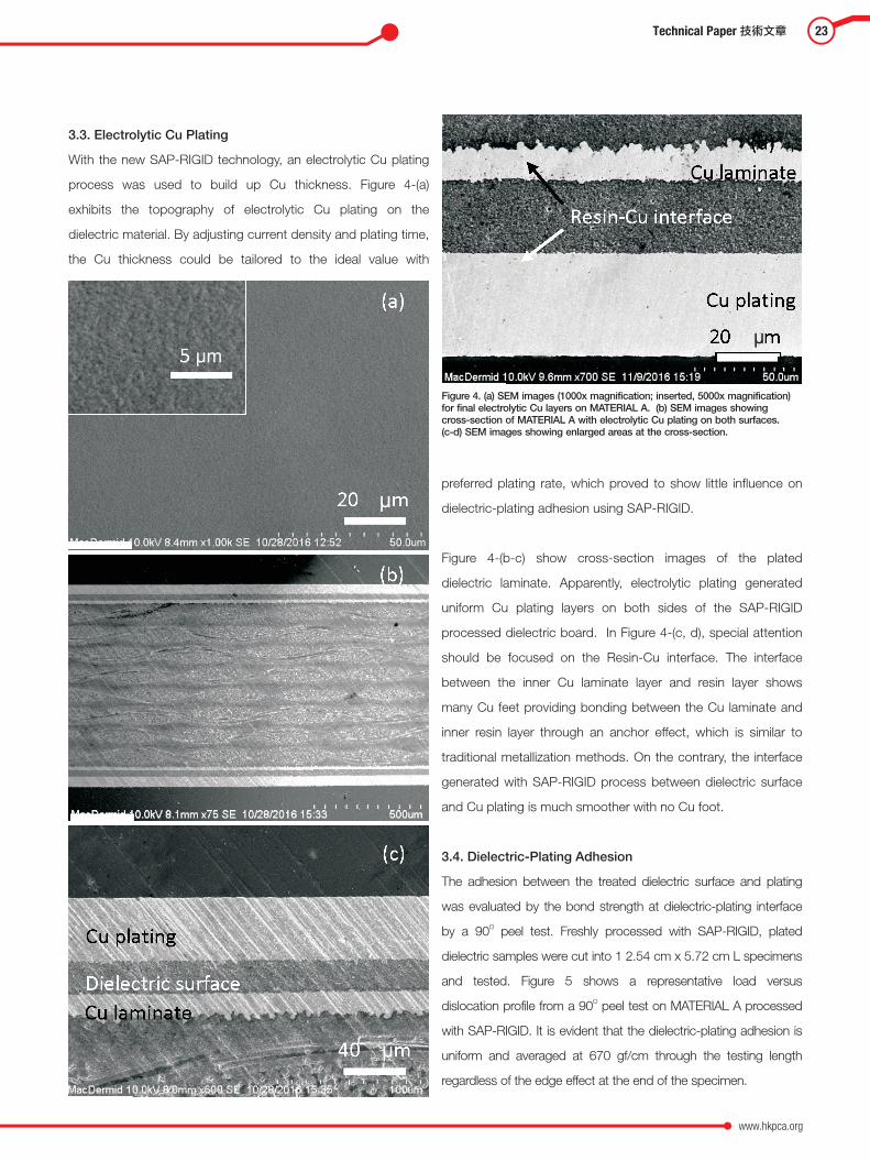
3.3. Electrolytic Cu Plating
With the new SAP-RIGID technology, an electrolytic Cu plating
process was used to build up Cu thickness. Figure 4-(a)
exhibits the topography of electrolytic Cu plating on the
dielectric material. By adjusting current density and plating time,
the Cu thickness could be tailored to the ideal value with
preferred plating rate, which proved to show little influence on
dielectric-plating adhesion using SAP-RIGID.
Figure 4-(b-c) show cross-section images of the plated
dielectric laminate. Apparently, electrolytic plating generated
uniform Cu plating layers on both sides of the SAP-RIGID
processed dielectric board. In Figure 4-(c, d), special attention
should be focused on the Resin-Cu interface. The interface
between the inner Cu laminate layer and resin layer shows
many Cu feet providing bonding between the Cu laminate and
inner resin layer through an anchor effect, which is similar to
traditional metallization methods. On the contrary, the interface
generated with SAP-RIGID process between dielectric surface
and Cu plating is much smoother with no Cu foot.
The adhesion between the treated dielectric surface and plating
was evaluated by the bond strength at dielectric-plating interface
by a 90 peel test. Freshly processed with SAP-RIGID, plated
dielectric samples were cut into 1 2.54 cm x 5.72 cm L specimens
and tested. Figure 5 shows a representative load versus
dislocation profile from a 90 peel test on MATERIAL A processed
with SAP-RIGID. It is evident that the dielectric-plating adhesion is
uniform and averaged at 670 gf/cm through the testing length
regardless of the edge effect at the end of the specimen.
3.4. Dielectric-Plating Adhesion
O
O
Figure 4. (a) SEM images (1000x magnification; inserted, 5000x magnification)
for final electrolytic Cu layers on MATERIAL A. (b) SEM images showing
cross-section of MATERIAL A with electrolytic Cu plating on both surfaces.
(c-d) SEM images showing enlarged areas at the cross-section.

Technical Paper24
Journal of the HKPCA / 2018 / Autumn / Issue No. 69
Figure 5. Representative load versus dislocation profile from 90 peel tests
showing dielectric-plating adhesion processed with SAP-RIGID on MATERIAL A
with electrolytic Cu plating around 20 m.
O
µ
Figure 6. Statistical analysis of dielectric-plating adhesion and capacity
evaluation of SAP-RIGID process on MATERIAL A with electrolytic Cu
plating around 20 m.µ
In order to evaluate the repeatability and consistency of the
adhesion, more replicate experiments were performed by
processing MATERIAL A using the SAP-RIGID process. At the
same time, the capacity of the SAP-RIGID process was
evaluated based on the adhesion results. As demonstrated in
Figure 6, using the SAP-RIGID process, the dielectric-plating
adhesion averages 658 18 gf/cm. Compared to a general
adhesion lower limit for the adhesion on MATERIAL A, which is
550 gf/cm, the SAP-RIGID process has a short-term capability
at 2.51 and a long-term capability of 2.06. In other words, our
SAP-RIGID process is a typical 6-sigma capable process,
which can consistently and continuously deliver satisfactory
adhesion.
±
3.5. Preliminary Application on other Dielectric Materials
In addition to investigation on MATERIAL A, some preliminary
studies were also carried out by applying the new SAP-RIGID
technique on other rigid dielectric materials (MATERIAL B,
MATERIAL C, MATERIAL D and MATERIAL E). The surface
morphology of these dielectric materials after SAP-RIGID
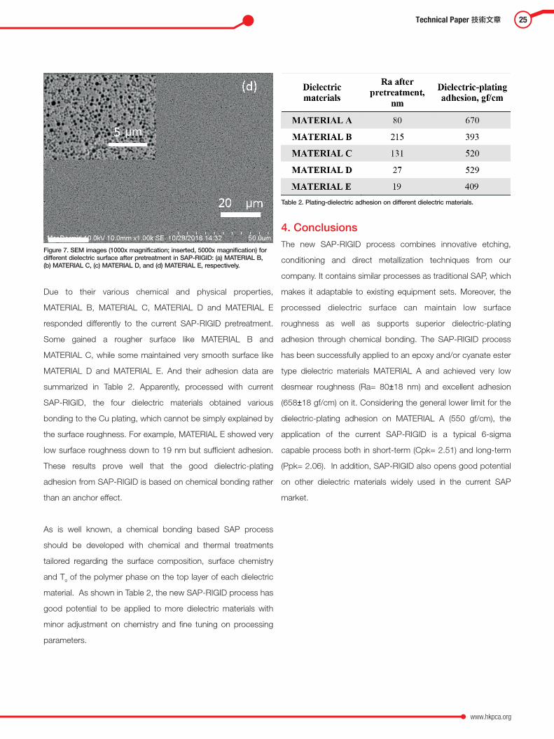
pretreatment are shown in Figure 7, respectively.
Technical Paper 25
www.hkpca.org
Figure 7. SEM images (1000x magnification; inserted, 5000x magnification) for
different dielectric surface after pretreatment in SAP-RIGID: (a) MATERIAL B,
(b) MATERIAL C, (c) MATERIAL D, and (d) MATERIAL E, respectively.
4. Conclusions
The new SAP-RIGID process combines innovative etching,
conditioning and direct metallization techniques from our
company. It contains similar processes as traditional SAP, which
makes it adaptable to existing equipment sets. Moreover, the
processed dielectric surface can maintain low surface
roughness as well as supports superior dielectric-plating
adhesion through chemical bonding. The SAP-RIGID process
has been successfully applied to an epoxy and/or cyanate ester
type dielectric materials MATERIAL A and achieved very low
desmear roughness (Ra= 80 18 nm) and excellent adhesion
(658 18 gf/cm) on it. Considering the general lower limit for the
dielectric-plating adhesion on MATERIAL A (550 gf/cm), the
application of the current SAP-RIGID is a typical 6-sigma
capable process both in short-term (Cpk= 2.51) and long-term
(Ppk= 2.06). In addition, SAP-RIGID also opens good potential
on other dielectric materials widely used in the current SAP
market.
±
±
Due to their various chemical and physical properties,
MATERIAL B, MATERIAL C, MATERIAL D and MATERIAL E
responded differently to the current SAP-RIGID pretreatment.
Some gained a rougher surface like MATERIAL B and
MATERIAL C, while some maintained very smooth surface like
MATERIAL D and MATERIAL E. And their adhesion data are
summarized in Table 2. Apparently, processed with current
SAP-RIGID, the four dielectric materials obtained various
bonding to the Cu plating, which cannot be simply explained by
the surface roughness. For example, MATERIAL E showed very
low surface roughness down to 19 nm but sufficient adhesion.
These results prove well that the good dielectric-plating
adhesion from SAP-RIGID is based on chemical bonding rather
than an anchor effect.
As is well known, a chemical bonding based SAP process
should be developed with chemical and thermal treatments
tailored regarding the surface composition, surface chemistry
and T of the polymer phase on the top layer of each dielectric
material. As shown in Table 2, the new SAP-RIGID process has
good potential to be applied to more dielectric materials with
minor adjustment on chemistry and fine tuning on processing
parameters.
g
Table 2. Plating-dielectric adhesion on different dielectric materials.


![SELECTIVE ELECTROLESS NICKEL PLATING ON OXYGEN …356823/FULLTEXT01.pdf · Electroless nickel plating on other, inactive seed-layers such as silicon [6, 7], aluminum [8] and ... displayed](https://img.dokumen.tips/doc/110x75/5f8284d6e56f510ad02498bb/selective-electroless-nickel-plating-on-oxygen-356823fulltext01pdf-electroless.jpg)