Embed Size (px)
Citation preview

20. Design for Testability
Jacob Abraham
Department of Electrical and Computer EngineeringThe University of Texas at Austin
VLSI DesignFall 2019
November 7, 2019
ECE Department, University of Texas at Austin Lecture 20. Design for Testability Jacob Abraham, November 7, 2019 1 / 38

Design for Testability (DFT)
Reduce costs associated with testing complex circuit
Design circuit so that it will be easier to test
Increase accessibility of internal nodes
Controllability: ability to establish specific signal value ateach internal node by setting inputsObservability: ability to determine internal values bycontrolling inputs and observing outputs
Ensure predictable circuit responses
Tradeoffs
Technical: area, I/O pins, performanceEconomic: design time, yield, time to revenue
ECE Department, University of Texas at Austin Lecture 20. Design for Testability Jacob Abraham, November 7, 2019 1 / 38

Testable Sequential Circuits
Sequential circuits are very difficult to test
Design the internal memoryelements to be part of ashifter register chain toprovide controllability,observability through serialshifts
With scan chain, problem of testing any circuit reduces to testingthe combinational logic
ECE Department, University of Texas at Austin Lecture 20. Design for Testability Jacob Abraham, November 7, 2019 2 / 38

Level-Sensitive Scan Design (LSSD)
Structured DFT developed at IBM
All internal storage implemented in hazard-free polarity-holdlatches (SRLs), part of a scan chain
Latches controlled by two or more non-overlapping clocks,with rules for clocking
All clock inputs to SRLs must be in their off states whenprimary inputs (PIs) are “off”Clock signal at any clock input to an SRL must be controlledfrom one or more clock PIsNo clock can be ANDed with another clockClock PIs cannot feed data inputs to latches, either directly orthrough combinational logic
ECE Department, University of Texas at Austin Lecture 20. Design for Testability Jacob Abraham, November 7, 2019 3 / 38

Scan Chains
Convert each flip-flop to a scan registerOnly costs one extra multiplexer
Normal mode: flip-flops behave as usual
Scan mode: flip-flops behave as shift register
Contents of flops can be scanned out and new values scannedin
ECE Department, University of Texas at Austin Lecture 20. Design for Testability Jacob Abraham, November 7, 2019 4 / 38

Scannable Flip-Flops
ECE Department, University of Texas at Austin Lecture 20. Design for Testability Jacob Abraham, November 7, 2019 5 / 38

Boundary Scan
Testing boards is also difficult
Need to verify solder joints are goodDrive a pin to 0, then to 1Check that all connected pins get the values
Single-sided PC boards with “through-hole” construction used“bed of nails” to contact pins of chip on the back side of theboard
SMT and BGA boards cannot easily contact pins
Build capability of observing and controlling pins into eachchip to make board test easier
ECE Department, University of Texas at Austin Lecture 20. Design for Testability Jacob Abraham, November 7, 2019 6 / 38

Boundary Scan (IEEE 1149.1)
ECE Department, University of Texas at Austin Lecture 20. Design for Testability Jacob Abraham, November 7, 2019 7 / 38

Boundary Scan Example
ECE Department, University of Texas at Austin Lecture 20. Design for Testability Jacob Abraham, November 7, 2019 8 / 38

Boundary Scan Interface
Boundary scan is accessed through five pins
TCK: test clockTMS: test mode selectTDI: test data inTDO: test data outTRST*: test reset (optional)
Chips with internal scan chains can access the chains throughboundary scan for unified test strategy
ECE Department, University of Texas at Austin Lecture 20. Design for Testability Jacob Abraham, November 7, 2019 9 / 38

IDDQ Testing
Measure quiescent power supply current of CMOS circuitsfor selected test vectors
Example, microprocessor has nanoamps of current with nofaults; many defects (shorts, for example) cause much highercurrents
Direct relationship found (Sandia Labs., HP, Phillips) betweenIDDQ test acceptance rates and quality, reliability of ICs
Only need to activate site of potential defect (no need topropagate errors)
Leakage current in very large chips may overwhelm the abnormalcurrent due to a fault in one gate
ECE Department, University of Texas at Austin Lecture 20. Design for Testability Jacob Abraham, November 7, 2019 10 / 38
IDDQ Testing, Cont’d
ECE Department, University of Texas at Austin Lecture 20. Design for Testability Jacob Abraham, November 7, 2019 11 / 38

Commercial Tool for DfT Insertion
Source: Synopsys, Inc.ECE Department, University of Texas at Austin Lecture 20. Design for Testability Jacob Abraham, November 7, 2019 12 / 38

Built-In Self Test (BIST)
Increasing circuit complexity, tester cost
Interest in techniques which integrate some tester capabilitieson the chip
Reduce tester costsTest circuits at speed (more thoroughly)
Approach:
Compress test responses into “signature”Pseudo-random (or pseudo-exhaustive) pattern generator(PRG) on the chip
Integrating pattern generation and response evaluationon chip – BIST
ECE Department, University of Texas at Austin Lecture 20. Design for Testability Jacob Abraham, November 7, 2019 13 / 38

Pseudo-Random Sequence Generator (PRSG)
Linear Feedback Shift Register
Shift register with input taken from XOR of statePseudo-Random Sequence Generator (or Pseudo-RandomPattern Generator (PRPG), or Linear Feedback Shift Register(LFSR))
Step Q0 1111 1102 1013 0104 1005 0016 0117 111 (repeats)
ECE Department, University of Texas at Austin Lecture 20. Design for Testability Jacob Abraham, November 7, 2019 14 / 38

Example of BIST
Technique calledSTUMPS (from IBM)
ECE Department, University of Texas at Austin Lecture 20. Design for Testability Jacob Abraham, November 7, 2019 15 / 38

Testability Techniques for 68020 ROMs
Used test mode to force next microcode address (NMA) fromdata pins
Data pins also control a MUX for both micro and nano ROMoutputs, which are moved to the BC bus, into the datasection of the execution unit, and to the address bus whichcan be observed
Exhaustive testing of the2K ROM entries
32 bits of ROM visibleevery 2 clocks
Four passes of testsneeded to read the 110outputs of the two ROMs
ECE Department, University of Texas at Austin Lecture 20. Design for Testability Jacob Abraham, November 7, 2019 16 / 38

Microrom Test in MC68881 Floating Point Co-processorROM physically split into two sectionsIn test mode, ROM is addressed directly through thecommand registerExhaustive addresses fed to ROM in a “ping-pong” fashion(address/address complement)Outputs of ROM go to two 16-bit signature registers (usingCCITT-16 polynomial x15 + x12 + x5 + 1)Monitor both the quotient and final signature serially on atest pin (Probability of aliasing 2−(n+m−1))
ECE Department, University of Texas at Austin Lecture 20. Design for Testability Jacob Abraham, November 7, 2019 17 / 38

MC68881 NanoROM Test
NanoROM physically located between the microROM and theexecution unit (ECU), and outputs fed to ECU
No functional path for nanoROM to access signature registers
In test mode, nanoROM columns coupled with the microROMcolumns (with additional columns of nanoROM multiplexed tosignature register)
ECE Department, University of Texas at Austin Lecture 20. Design for Testability Jacob Abraham, November 7, 2019 18 / 38

MC68881 Entry PLA Test
Four entry PLAs, A0, A1, A2 and A3
A0 PLA contains the entry point reset vectors and iscompletely tested functionallyA1–A3 tested like the ROMs
Command register generatespatterns and outputs are routedthrough a bus to the signatureregister
Test patterns generated using PLAtest generator
PLA Inputs Outputs Products
A1 6 10 23A2 13 10 133A3 5 10 28Response 25 25 56
ECE Department, University of Texas at Austin Lecture 20. Design for Testability Jacob Abraham, November 7, 2019 19 / 38

Built-in Self Test in the Intel 80386
Normal PLA inputs disabled during test and output ofpseudorandom generator provides exhaustive set of tests toAND-plane input
CROM tested with binary counter (exhaustive test)
Responses compressed using multiple-input signature registers
Test transistors: 2.7%
Area overhead for BIST:1.8%
Transistor sites testedwith BIST: 52.5%
Area tested: 18.6%
ECE Department, University of Texas at Austin Lecture 20. Design for Testability Jacob Abraham, November 7, 2019 20 / 38

Testing Cache Memory Arrays in MC68030
Cache cell layout design is resistant to both bridging defectsand capacitive coupling
Most likely bridging defect is between adjacent metal bit linesMemory fault model:
One or more cells stuck at 0 or 1Coupling between cells
11n March Test (Marinescu, 1982)
Refresh and data retention tests for the dynamic memory cellsECE Department, University of Texas at Austin Lecture 20. Design for Testability Jacob Abraham, November 7, 2019 21 / 38

MC68040 Scan Chain and Timing
ECE Department, University of Texas at Austin Lecture 20. Design for Testability Jacob Abraham, November 7, 2019 22 / 38

BIST in IBM Risc System/6000
LSSD with pseudo-random BIST
ECE Department, University of Texas at Austin Lecture 20. Design for Testability Jacob Abraham, November 7, 2019 23 / 38
Common Engineering Processor (COP), bus, on-card sequencer (OCS), engineering support processor (ESP)

Common on-chip Processor (COP) in IBM RS/6000
Hardware for pseudo-random vector generation and resultcompression (31-bit LFSR)
ECE Department, University of Texas at Austin Lecture 20. Design for Testability Jacob Abraham, November 7, 2019 24 / 38
Small processor controls operation
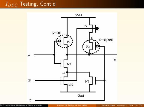
BIST in IBM/Motorola Power-PC
Variety of test techniques applied to the Power-PC 603
Full LSSD test of logicBIST of “large” embedded RAMSFunctional test of small RAMSIDDQ tests
BIST for cache and tag RAMs
Functional vectors (good for data cache, not instruction cache)and random BIST (size, complexity, test coverage) notapplicable
Use modified march test of Dekker (1988)
log2 n pattern for data
Overhead: BIST is 2.9% of RAM array, 0.58% of total chip
Performance impact: less than 100 pS due to extra MUXinput leg
All four RAMs tested in parallel, 2.5 mS at 80 MHz
ECE Department, University of Texas at Austin Lecture 20. Design for Testability Jacob Abraham, November 7, 2019 25 / 38
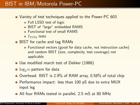
Issues with Built-In Self Test
Technique can run test sequences at operating frequencies andcapture results within the chip
Pseudorandom pattern generators, signature analyzers
Can also use weighted randompatterns or deterministic patterns
Example (Synopsys): DeterministicLogic BIST
Problems:Hardware overheadTest powerNon-functional modes during test
ECE Department, University of Texas at Austin Lecture 20. Design for Testability Jacob Abraham, November 7, 2019 26 / 38

Industry Issues with Processor Testing
Concern with detecting real defects
Small delay defects due to process variations, power droopsand capacitive coupling
Cause a shift in the speed of the part
Problems with logic BIST (same issues with scan AC tests)
Overheads on chip
False paths tested
Test operating conditions different from normal operatingmodes
ECE Department, University of Texas at Austin Lecture 20. Design for Testability Jacob Abraham, November 7, 2019 27 / 38

Software-Based (Native-Mode) Self Test for Processors
Why not use functional capabilities of processors to replaceBIST hardware?
No additional hardware
Reduce test costs by using low-cost testers
Increase coverage of delay defects and increase yield by testingnative
No issues with excessive power consumption during test
Developed at University of Texas (Int’l Test Conference 1998)
Application to processors at Intel (Int’l Test Conference 2002)
ECE Department, University of Texas at Austin Lecture 20. Design for Testability Jacob Abraham, November 7, 2019 28 / 38
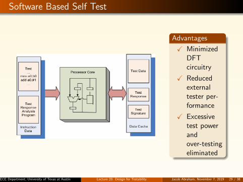
Software Based Self Test
Advantages
X MinimizedDFTcircuitry
X Reducedexternaltester per-formance
X Excessivetest powerandover-testingeliminated
ECE Department, University of Texas at Austin Lecture 20. Design for Testability Jacob Abraham, November 7, 2019 29 / 38
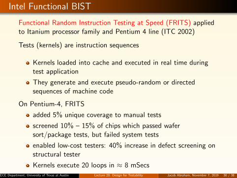
Intel Functional BIST
Functional Random Instruction Testing at Speed (FRITS) appliedto Itanium processor family and Pentium 4 line (ITC 2002)
Tests (kernels) are instruction sequences
Kernels loaded into cache and executed in real time duringtest application
They generate and execute pseudo-random or directedsequences of machine code
On Pentium-4, FRITS
added 5% unique coverage to manual tests
screened 10% – 15% of chips which passed wafersort/package tests, but failed system tests
enabled low-cost testers: 40% increase in defect screening onstructural tester
Kernels execute 20 loops in ≈ 8 mSecsECE Department, University of Texas at Austin Lecture 20. Design for Testability Jacob Abraham, November 7, 2019 30 / 38

Are Random Tests Sufficient?
Intel implementation involved code in the cache which generatedrandom instruction sequences
Interest in generating instructions targeting faults
Possible to generate instruction sequences which will test foran internal stuck-at fault in a module
In order to deal with defects in DSM technologies, need to targetsmall delay defects
Automatically generate instruction sequences which willtarget small delay defects in an internal module
ECE Department, University of Texas at Austin Lecture 20. Design for Testability Jacob Abraham, November 7, 2019 31 / 38

RT Level Test Generation for Hard-to Detect Faults
Overview
Map gate level stuck-at faultto RTL
Capture the propagationconstraints as an LTLproperty
Generate a witness for theLTL property using BoundedModel Checking
All required constraintsavailable in RTL
Use SMT based BoundedModel Checking
Scaling with
cone-of-influence reduction
ECE Department, University of Texas at Austin Lecture 20. Design for Testability Jacob Abraham, November 7, 2019 32 / 38

RTL Test Generation for Hard-to-Detect Faults
Experimental Setup
OR1200 RISC processor was DUT
EBMC Model checker / Boolector SMT solver
Bound of pipleine depth + 1
Focused on hard to detect faults in control logic
Commercial ATPG to seive out easy to detect stuck-at faults
78% Fault coverage by commercial ATPG
ECE Department, University of Texas at Austin Lecture 20. Design for Testability Jacob Abraham, November 7, 2019 33 / 38

RT Level Test Generation for Hard-to Detect Faults
Experimental Results using SMT Solver
Module ATPGFC(%)
Flts.SAT basedmethod
Naive ObservabilityMethod
FC(%) # TO T(sec) FC(%) # TO T(sec)
if 80.35 328 84.11 310 96.18 88.49 161 95.13ctrl 63.21 832 65.97 817 83.12 97.15 59 69.72
oprmux 73.66 378 76.09 354 95.49 98.26 6 57.46sprs 89.59 393 90.85 381 93.71 93.78 57 90.27
freeze 82.94 17 99.14 2 64.41 100 0 43.51rf 78.59 7444 80.50 7268 97.57 90.21 463 69.83
except 72.69 1263 73.48 1209 98.63 92.79 128 96.19
Overall 78.05 10655 79.17 10343 96.23 93.86 874 76.11
FC(%) : Fault Coverage in %# TO : # of Timed Out faults
T(sec) : Average Time for generating a test for a fault in secondsECE Department, University of Texas at Austin Lecture 20. Design for Testability Jacob Abraham, November 7, 2019 34 / 38
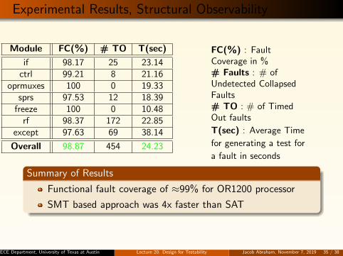
Experimental Results, Structural Observability
Module FC(%) # TO T(sec)
if 98.17 25 23.14ctrl 99.21 8 21.16
oprmuxes 100 0 19.33sprs 97.53 12 18.39
freeze 100 0 10.48rf 98.37 172 22.85
except 97.63 69 38.14
Overall 98.87 454 24.23
FC(%) : FaultCoverage in %# Faults : # ofUndetected CollapsedFaults# TO : # of TimedOut faults
T(sec) : Average Time
for generating a test for
a fault in seconds
Summary of Results
Functional fault coverage of ≈99% for OR1200 processor
SMT based approach was 4x faster than SAT
ECE Department, University of Texas at Austin Lecture 20. Design for Testability Jacob Abraham, November 7, 2019 35 / 38
Detecting Delay Defects After Manufacturing
Necessary to detect “small-delay defects”
Delay defects which don’t affect performance soon aftermanufacture could be reliability hazards
Need Path Delay Tests to ensure that defective parts arescreened out
Difficult to apply two-pattern tests in scan modeRequires precise control of clocks for high-speed circuitsIf capture clocks are based on the system clock, there is noinformation on the slack for the path
Solution: On-chip programmable capture mechanismAbility to capture faster than at-speed
ECE Department, University of Texas at Austin Lecture 20. Design for Testability Jacob Abraham, November 7, 2019 36 / 38

Delay Lines for On-Chip Programmable Capture
Source: R. Tayade, et al.ECE Department, University of Texas at Austin Lecture 20. Design for Testability Jacob Abraham, November 7, 2019 37 / 38

System for On-Chip Programmable Capture
Source: R. Tayade, et al.ECE Department, University of Texas at Austin Lecture 20. Design for Testability Jacob Abraham, November 7, 2019 38 / 38