Embed Size (px)
Citation preview

General DescriptionThe MAX8896 dual step-down converter is optimizedfor powering the power amplifier (PA) and RF transceiv-er in WCDMA handsets. This device integrates a high-efficiency PWM step-down converter (OUT1) formedium and low-power transmission, and a 140mΩ(typ) bypass FET to power the PA directly from the bat-tery during high-power transmission. A second high-efficiency PWM step-down converter (OUT2) suppliespower directly to a high PSRR, low output noise, 200mAlow-dropout linear regulator (LDO) to power the RFtransceiver.
Fast switching allows the use of small ceramic input andoutput capacitors while maintaining low ripple voltage.The feedback network is integrated reducing externalcomponent count and total solution size. OUT1 uses ananalog input driven by an external DAC to control theoutput voltage linearly for continuous PA power adjust-ment. At high duty cycle, OUT1 automatically switches tobypass mode, connecting the input to the output througha low-impedance (140mΩ, typ) MOSFET.
OUT2 is a 2MHz fixed-frequency, step-down convertercapable of operating at 100% duty cycle. Output accu-racy is ±2% over load, line, and temperature. The out-put of OUT2 is preset to 3.1V to provide power to a200mA, 2.8V LDO designed for low noise (16µVRMS,typ), high PSRR (65dB, typ) operation. This configura-tion provides noise attenuation for the RF transceiverpower supply in the 100Hz to 100kHz range.
Other features include separate output enables, low-supply current shutdown, output overcurrent, andovertemperature protection. The MAX8896 is availablein a 16-bump, 2mm x 2mm UCSP™ package (0.7mmmax height).
ApplicationsWCDMA/NCDMA Cellular Handsets
Smartphones
Features PA Step-Down Converter (OUT1)
7.5µs (typ) Settling Time for 0.5V to 1V OutputVoltage Change
Dynamic Output Voltage Setting from 0.5V toVBATT
140mΩ Bypass PFET and 100% Duty Cycle for Low Dropout
2MHz Switching FrequencyLow Output Voltage Ripple700mA (min) Output Drive Capability2% Gain AccuracyTiny External Components
RF Step-Down Converter (OUT2)2MHz Fixed Switching Frequency94% Peak Efficiency100% Duty Cycle2% Output Accuracy Over Load, Line, and
Temperature200mA (min) Output Drive CapabilityTiny External Components
Low-Noise LDOGuaranteed 200mA OutputHigh 65dB (typ) PSRRFixed Output VoltageLow Noise (16µVRMS, typ)
Simple Logic ON/OFF Controls
Low 0.1µA Shutdown Current
2.7V to 5.5V Supply Voltage Range
Thermal Shutdown
2mm x 2mm UCSP Package (4 x 4 Grid)
MA
X8
89
6
Dual PWM Step-Down Converter in a 2mm x2mm Package for WCDMA PA and RF Power
________________________________________________________________ Maxim Integrated Products 1
19-4663; Rev 0; 5/09
EVALUATION KIT
AVAILABLE
UCSP is a trademark of Maxim Integrated Products, Inc. Pin Configurations appear at end of data sheet.
Ordering Information
PART PIN-PACKAGELDO
VOLTAGE
MAX8896EREE+T 16 UCSP (0.5mm pitch) 2.80V
Note: Device operates over the -40°C to +85°C temperaturerange.+Denotes a lead(Pb)-free/RoHS-compliant package.T = Tape and reel.
For information on other Maxim products, visit Maxim’s website at www.maxim-ic.com.

MA
X8
89
6
Dual PWM Step-Down Converter in a 2mm x2mm Package for WCDMA PA and RF Power
2 _______________________________________________________________________________________
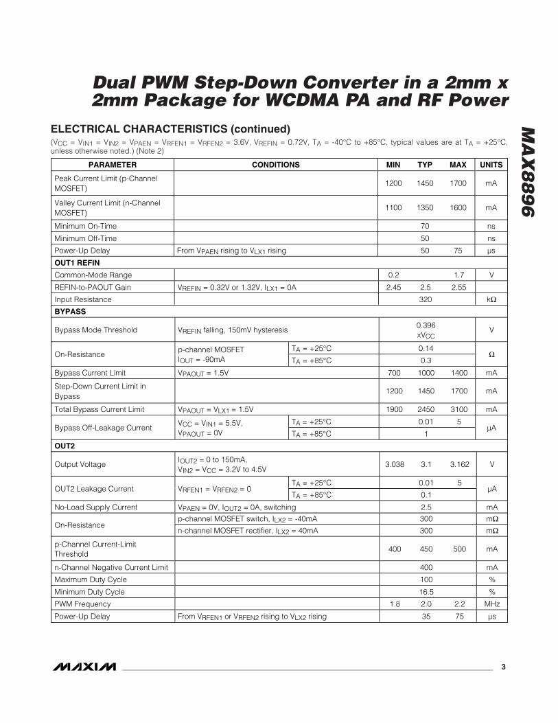
ELECTRICAL CHARACTERISTICS(VCC = VIN1 = VIN2 = VPAEN = VRFEN1 = VRFEN2 = 3.6V, VREFIN = 0.72V, TA = -40°C to +85°C, typical values are at TA = +25°C,unless otherwise noted.) (Note 2)
Stresses beyond those listed under “Absolute Maximum Ratings” may cause permanent damage to the device. These are stress ratings only, and functionaloperation of the device at these or any other conditions beyond those indicated in the operational sections of the specifications is not implied. Exposure toabsolute maximum rating conditions for extended periods may affect device reliability.
PARAMETER CONDITIONS MIN TYP MAX UNITS
INPUT SUPPLY
Input Voltage VCC, VIN1, VIN2 2.7 5.5 V
Input Undervoltage Threshold VCC rising, 180mV typical hysteresis 2.52 2.63 2.70 V
TA = +25°C 0.1 4Shutdown Supply Current V P AE N = V R FE N 1 = V R FE N 2 = 0
TA = +85°C 0.1µA
LOGIC CONTROL
PAEN, RFEN1, RFEN2 LogicInput High Voltage
2.7V ≤ VCC ≤ 5.5V 1.3 V
PAEN, RFEN1, RFEN2 LogicInput Low Voltage
2.7V ≤ VCC ≤ 5.5V 0.4 V
PAEN, RFEN1, RFEN2 InternalPulldown Resistor
400 800 1600 kΩ
TA = +25°C 0.01 1PAEN, RFEN1, RFEN2 LogicInput Current
VIL = 0TA = +85°C 0.1
µA
REFBP
REFBP Output Voltage 0µA ≤ IREFBP ≤ 1µA 1.237 1.250 1.263 V
THERMAL PROTECTION
Thermal Shutdown TA rising, 20°C typical hysteresis +160 °C
OUT1
Quiescent Supply CurrentVRFEN1 = VRFEN2 = 0V, IPA = 0A,no switching
155 µA
p-channel MOSFET switch, ILX1 = -200mA 0.16 0.40On-Resistance
n-channel MOSFET rectifier, ILX1 = 500mA 0.17 0.40Ω
Load Regulation RL is the inductor resistance RL/2 V/A
TA = +25°C 0.1 5LX1 Leakage Current VIN1 = 5.5V, VLX1 = 0V
TA = +85°C 1µA
ABSOLUTE MAXIMUM RATINGSVCC, IN1, IN2, PAEN, RFEN1, RFEN2,
REFIN, OUT2, REFBP to AGND .........................-0.3V to +6.0VPAOUT to AGND........................................-0.3V to (VIN1 + 0.3V)LDO to AGND .........................................-0.3V to (VOUT2 + 0.3V)IN1, IN2 to VCC......................................................-0.3V to +0.3VIN1 to IN2 ..............................................................-0.3V to +0.3VPGND1, PGND2 to AGND.....................................-0.3V to +0.3VLX1 Current .......................................................................1ARMSLX2 Current .......................................................................1ARMSIN1 and PAOUT Current....................................................1ARMS
PAOUT, OUT2, LDO Short Circuit to PGND1, PGND2 ....................................................................Continuous
Continuous Power Dissipation (TA = +70°C)16-Bump UCSP (derate 12.5mW/°C above +70°C) ............1W
Junction-to-Ambient Thermal Resistance (θJA) (Note 1)...96°C/WJunction Temperature ......................................................+150°CStorage Temperature Range .............................-65°C to +150°CBump Temperature (soldering, reflow) ...........................+260°C
Note 1: Package thermal resistances were obtained using the method described in JEDEC specification JESD51-7, using a four-layer board. For detailed information on package thermal considerations, refer to www.maxim-ic.com/thermal-tutorial.
MA
X8
89
6
Dual PWM Step-Down Converter in a 2mm x2mm Package for WCDMA PA and RF Power
_______________________________________________________________________________________ 3
PARAMETER CONDITIONS MIN TYP MAX UNITS
Peak Current Limit (p-ChannelMOSFET)
1200 1450 1700 mA
Valley Current Limit (n-ChannelMOSFET)
1100 1350 1600 mA
Minimum On-Time 70 ns
Minimum Off-Time 50 ns
Power-Up Delay From VPAEN rising to VLX1 rising 50 75 µs
OUT1 REFIN
Common-Mode Range 0.2 1.7 V
REFIN-to-PAOUT Gain VREFIN = 0.32V or 1.32V, ILX1 = 0A 2.45 2.5 2.55
Input Resistance 320 kΩBYPASS
Bypass Mode Threshold VREFIN falling, 150mV hysteresis0.396xVCC
V
TA = +25°C 0.14On-Resistance
p-channel MOSFETIOUT = -90mA TA = +85°C 0.3
Ω
Bypass Current Limit VPAOUT = 1.5V 700 1000 1400 mA
Step-Down Current Limit inBypass
1200 1450 1700 mA
Total Bypass Current Limit VPAOUT = VLX1 = 1.5V 1900 2450 3100 mA
TA = +25°C 0.01 5Bypass Off-Leakage Current
VCC = VIN1 = 5.5V,VPAOUT = 0V TA = +85°C 1
µA
OUT2
Output VoltageIOUT2 = 0 to 150mA,VIN2 = VCC = 3.2V to 4.5V
3.038 3.1 3.162 V
TA = +25°C 0.01 5OUT2 Leakage Current VRFEN1 = VRFEN2 = 0
TA = +85°C 0.1µA
No-Load Supply Current VPAEN = 0V, IOUT2 = 0A, switching 2.5 mA
p-channel MOSFET switch, ILX2 = -40mA 300 mΩOn-Resistance
n-channel MOSFET rectifier, ILX2 = 40mA 300 mΩ
p-Channel Current-LimitThreshold
400 450 500 mA
n-Channel Negative Current Limit 400 mA
Maximum Duty Cycle 100 %
Minimum Duty Cycle 16.5 %
PWM Frequency 1.8 2.0 2.2 MHz
Power-Up Delay From VRFEN1 or VRFEN2 rising to VLX2 rising 35 75 µs
ELECTRICAL CHARACTERISTICS (continued)(VCC = VIN1 = VIN2 = VPAEN = VRFEN1 = VRFEN2 = 3.6V, VREFIN = 0.72V, TA = -40°C to +85°C, typical values are at TA = +25°C,unless otherwise noted.) (Note 2)

MA
X8
89
6
Dual PWM Step-Down Converter in a 2mm x2mm Package for WCDMA PA and RF Power
4 _______________________________________________________________________________________
ELECTRICAL CHARACTERISTICS (continued)(VCC = VIN1 = VIN2 = VPAEN = VRFEN1 = VRFEN2 = 3.6V, VREFIN = 0.72V, TA = -40°C to +85°C, typical values are at TA = +25°C,unless otherwise noted.) (Note 2)
PARAMETER CONDITIONS MIN TYP MAX UNITS
LDO
Output Voltage, VLDO VOUT2 = 3.1V, ILDO = 1mA to 200mA 2.744 2.800 2.856 V
Current Limit VOUT2 = 3.1V, VLDO = 0V 250 420 750 mA
Dropout Voltage VOUT2 = 3.1V, ILDO = 100mA 70 mV
Line Regulation VOUT2 stepped from 3.5V to 5.5V, ILDO = 100mA 2.4 mV
Load Regulation VOUT2 = 3.1V, ILDO stepped from 50µA to 200mA 25 mV
Power-Supply Rejection∆VLDO/∆VOUT2
VOUT2 = 3.1V, 10Hz to 10kHz,CLDO = 1µF, ILDO = 100mA
65 dB
Output Noise100Hz to 100kHz,CLDO = 1µF, ILDO = 100mA
16 µVRMS
Minimum Output Capacitance forStable Operation
0 < ILDO < 200mA 1 µF
Output Leakage Current VOUT2 = 3.1V, VRFEN1 = VRFEN2 = 0V 25 nA
Power-Up Delay From VRFEN1 or VRFEN2 rising to VLDO rising 50 µs
Note 2: All devices are 100% production tested at TA = +25°C. Limits over the operating temperature range are guaranteed bydesign.
MA
X8
89
6
Dual PWM Step-Down Converter in a 2mm x2mm Package for WCDMA PA and RF Power
_______________________________________________________________________________________ 5
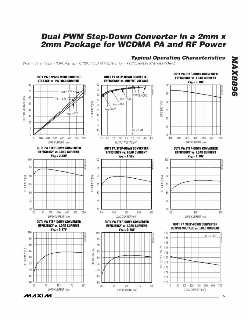
0
20
10
40
30
70
60
50
80
0 200100 300 400 500 600 700
OUT1 PA BYPASS MODE DROPOUTVOLTAGE vs. PA LOAD CURRENT
MAX
8896
toc0
1
LOAD CURRENT (mA)
DROP
OUT
VOLT
AGE
(mV)
VIN1 = 3.2V
VIN1 = 3.6V
VIN1 = 4.2V
0
20
10
40
30
60
50
70
90
80
100
0.5 1.5 2.01.0 2.5 3.0 3.5 4.0 4.5
OUT1 PA STEP-DOWN CONVERTEREFFICIENCY vs. OUTPUT VOLTAGE
MAX
8896
oc0
2
OUTPUT VOLTAGE (V)
EFFI
CIEN
CY (%
)BYPASS MODE
VIN1 = 4.2V
VIN1 = 3.6V
VIN1 = 3.2V
RPA = 7.5Ω
70
85
80
75
95
90
100
100 200 300 400 500 600 700
OUT1 PA STEP-DOWN CONVERTEREFFICIENCY vs. LOAD CURRENT
VPA = 3.18V
MAX
8896
toc0
3
LOAD CURRENT (mA)
EFFI
CIEN
CY (%
)
70
75
95
90
85
80
100
50 150 250 350 450 550 650
OUT1 PA STEP-DOWN CONVERTEREFFICIENCY vs. LOAD CURRENT
VPA = 2.58V
MAX
8896
toc0
4
LOAD CURRENT (mA)
EFFI
CIEN
CY (%
)
70
75
95
90
85
80
100
50 150 250 350 450
OUT1 PA STEP-DOWN CONVERTEREFFICIENCY vs. LOAD CURRENT
VPA = 1.58VM
AX88
96 to
c05
LOAD CURRENT (mA)
EFFI
CIEN
CY (%
)
70
75
95
90
85
80
100
50 150 250
OUT1 PA STEP-DOWN CONVERTEREFFICIENCY vs. LOAD CURRENT
VPA = 1.18V
MAX
8896
toc0
6
LOAD CURRENT (mA)
EFFI
CIEN
CY (%
)
60
75
65
70
85
80
95
90
100
25 75 125 175 225
OUT1 PA STEP-DOWN CONVERTEREFFICIENCY vs. LOAD CURRENT
VPA = 0.77V
MAX
8896
toc0
7
LOAD CURRENT (mA)
EFFI
CIEN
CY (%
)
OUT1 PA STEP-DOWN CONVERTEREFFICIENCY vs. LOAD CURRENT
VPA = 0.56V
MAX
8896
toc0
8
60
75
65
70
85
80
95
90
100
25 75 125 175 225LOAD CURRENT (mA)
EFFI
CIEN
CY (%
)
1.70
1.76
1.74
1.72
1.80
1.78
1.88
1.86
1.84
1.82
1.90
0 100 200 300 400 500 600 700
OUT1 PA STEP-DOWN CONVERTEROUTPUT VOLTAGE vs. LOAD CURRENT
MAX
8896
toc0
9
LOAD CURRENT (mA)
OUTP
UT V
OLTA
GE (V
)
RL = 0.09Ω
Typical Operating Characteristics(VCC = VIN1 = VIN2 = 3.6V, VREFIN = 0.72V, circuit of Figure 3, TA = +25°C, unless otherwise noted.)

MA
X8
89
6
Dual PWM Step-Down Converter in a 2mm x2mm Package for WCDMA PA and RF Power
6 _______________________________________________________________________________________
Typical Operating Characteristics (continued)(VCC = VIN1 = VIN2 = 3.6V, VREFIN = 0.72V, circuit of Figure 3, TA = +25°C, unless otherwise noted.)
0.5
1.5
1.0
2.5
2.0
3.5
3.0
4.0
0.2 0.6 0.80.4 1.0 1.2 1.4 1.6 1.8 2.0
OUT1 PA STEP-DOWN CONVERTER OUTPUTVOLTAGE vs. REFIN VOLTAGE
MAX
8896
toc1
0
REFIN VOLTAGE (V)
OUTP
UT V
OLTA
GE (V
)
OUTPUT VOLTAGE ERRORvs. LOAD CURRENT
MAX
8896
toc1
1
-4
-1
-3
-2
1
0
3
2
4
0 200100 400 600300 500 700 800LOAD CURRENT (mA)
OUTP
UT V
OLTA
GE E
RROR
(%)
VOUT = 3.18V
VOUT = 0.56V
OUT1 LIGHT-LOAD SWITCHINGWAVEFORMS
MAX8896 toc12
VLX1
IL1
VPA
2V/div
200mA/div
20mV/div(AC-COUPLED)
200ns/div
5mA LOAD
200ns/div
OUT1 HEAVY-LOAD SWITCHINGWAVEFORMS
ILX1 200mA/div
20mV/div(AC-COUPLED)
2V/div
MAX8896 toc13
VPA
VLX1
500mA LOAD
20µs/div
OUT1 STARTUP AND SHUTDOWN
VPAEN5V/div
1V/div
500mA/div
MAX8896 toc14
VPA
IL1

MA
X8
89
6
Dual PWM Step-Down Converter in a 2mm x2mm Package for WCDMA PA and RF Power
_______________________________________________________________________________________ 7
10µs/div
OUT1 LOAD TRANSIENT RESPONSE
IOUT
200mA/div
100mV/div(AC-COUPLED)
MAX8896 toc16
VPA
500mA
0mA
10µs/div
OUT1 REFIN TRANSIENT RESPONSE
VREFIN
500mV/div
500mV/div
1A/div
MAX8896 toc17
VPA
IL1
0.72V
0.2V 1.8V
0.5V
2.5Ω LOAD
10µs/div
OUT1 REFIN TRANSIENT RESPONSEWITH BYPASS EVENT
VREFIN 1V/div
1V/div
1A/div
MAX8896 toc18
VPA
IL1
3.3V0.6V
1.8V
0
30
20
10
40
50
60
70
80
90
100
0 50 100 150 200
OUT2 EFFICIENCYvs. LOAD CURRENT
MAX
8896
toc1
9
LOAD CURRENT (mA)
EFFI
CIEN
CY (%
)
VCC = 4.2VVCC = 3.6V
VCC = 3.2V
20µs/div
OUT1 LINE TRANSIENT RESPONSE
VIN500mV/div
10mV/div(AC-COUPLED)
200mA/div
MAX8896 toc15
VPA
IL1
50mA LOAD
4.0V
3.5V
Typical Operating Characteristics (continued)(VCC = VIN1 = VIN2 = 3.6V, VREFIN = 0.72V, circuit of Figure 3, TA = +25°C, unless otherwise noted.)
3.04
3.05
3.06
3.07
3.08
3.09
3.10
3.11
3.12
0 50 100 150 200
*OUT2 IN DROPOUT
OUT2 VOLTAGEvs. LOAD CURRENT
MAX
8896
toc2
0
LOAD CURRENT (mA)
OUTP
UT V
OLTA
GE (V
)
VCC = 3.6V
VCC = 3.2V*
VCC = 4.2V
10µs/div
OUT2 LOAD TRANSIENT RESPONSE
100mA/div
MAX8896 toc25
IOUT2
VOUT2100mV/div(AC-COUPLED)
150mA
0mA
0
0.06
0.04
0.02
0.08
0.10
0.12
0.14
0.16
0.18
0.20
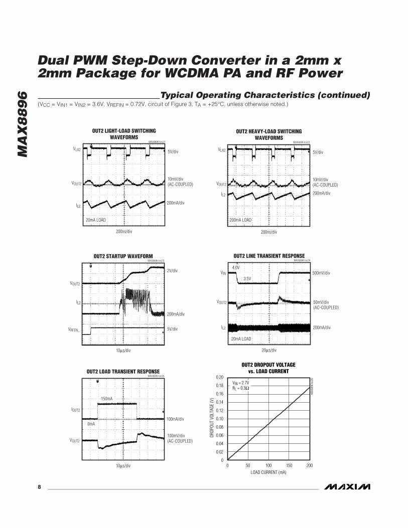
0 50 100 150 200
OUT2 DROPOUT VOLTAGEvs. LOAD CURRENT
MAX
8896
toc2
6
LOAD CURRENT (mA)
DROP
OUT
VOLT
AGE
(V)
VIN = 2.7VRL = 0.3Ω
MA
X8
89
6
Dual PWM Step-Down Converter in a 2mm x2mm Package for WCDMA PA and RF Power
8 _______________________________________________________________________________________
200ns/div
OUT2 HEAVY-LOAD SWITCHINGWAVEFORMS
VLX2
10mV/div(AC-COUPLED)
5V/div
200mA/div
MAX8896 toc22
VOUT2
IL2
200mA LOAD
10µs/div
OUT2 STARTUP WAVEFORM
VOUT2
2V/div
200mA/div
MAX8896 toc23
IL2
VRFEN_ 5V/div
Typical Operating Characteristics (continued)(VCC = VIN1 = VIN2 = 3.6V, VREFIN = 0.72V, circuit of Figure 3, TA = +25°C, unless otherwise noted.)
20µs/div
OUT2 LINE TRANSIENT RESPONSE
VIN 500mV/div
200mA/div
MAX8896 toc24
VOUT2
IL2
50mV/div(AC-COUPLED)
4.0V
3.5V
20mA LOAD
200ns/div
OUT2 LIGHT-LOAD SWITCHINGWAVEFORMS
VLX2
10mV/div(AC-COUPLED)
5V/div
200mA/div
MAX8896 toc21
VOUT2
IL2
20mA LOAD

MA
X8
89
6
2.76
2.78
2.77
2.80
2.79
2.81
2.82
0 10050 150 250200
LDO OUTPUT VOLTAGEvs. LOAD CURRENT
MAX
8896
toc2
7
LOAD CURRENT (mA)
OUTP
UT V
OLTA
GE (V
)
0
0.06
0.04
0.02
0.08
0.10
0.12
0.14
0.16
0.18
0.20
0 50 100 150 200
LDO DROPOUT VOLTAGEvs. LOAD CURRENT
MAX
8896
toc2
8
LOAD CURRENT (mA)
DROP
OUT
VOLT
AGE
(V)
VOUT2 = 2.7V
4µs/div
LDO LOAD TRANSIENT RESPONSE
50mA/div
MAX8896 toc29
VLDO
ILDO
20mV/div(AC-COUPLED)
80mA
10mA
VRFEN1
VOUT2
VLDO
200mA LOAD ON LDO
400µs/div
LDO STARTUP WAVEFORMMAX8896 toc30
2V/div
2V/div
2V/div
400µs/div
LDO OUTPUT NOISE(OUT1, OUT2, AND LDO ENABLED)
MAX8896 toc31
VLDO
30mA LOAD
10µV/div
LDO OUTPUT-NOISE SPECTRALDENSITY vs. FREQUENCY
(OUT1, OUT2, AND LDO ENABLED)
MAX
8896
toc3
2
FREQUENCY (kHz)1,0001001010.1
10E+0
100E+0
1E+3
10E+3
1E+00.01 10,000
NOIS
E DE
NSIT
Y (n
V/√H
z)
Typical Operating Characteristics (continued)(VCC = VIN1 = VIN2 = 3.6V, VREFIN = 0.72V, circuit of Figure 3, TA = +25°C, unless otherwise noted.)
Dual PWM Step-Down Converter in a 2mm x2mm Package for WCDMA PA and RF Power
_______________________________________________________________________________________ 9

MA
X8
89
6
Dual PWM Step-Down Converter in a 2mm x2mm Package for WCDMA PA and RF Power
10 ______________________________________________________________________________________
Pin DescriptionPIN NAME FUNCTION
A1 REFBPReference Noise Bypass. Bypass REFBP to AGND with a 0.033µF ceramic capacitor to reduce noiseon the LDO output. REFBP is internally pulled down through a 1kΩ resistor during shutdown.
A2 AGNDLow-Noise Analog Ground. Connect AGND to the ground plane at a single point away from highswitching currents. See the PCB Layout section.
A3 REFINDAC-Controlled Input. The output of the PA step-down converter is regulated to 2.5 x VREFIN. WhenVREFIN reaches 0.396 x VCC, bypass mode is enabled.
A4 PGND1Power Ground for OUT1. Connect PGND1 to the ground plane near the input and output capacitorgrounds. See the PCB Layout section.
B1 LDO200mA LDO Regulator Output. Bypass LDO with a 1µF ceramic capacitor as close as possible toLDO and ground. Leave LDO unconnected if not used.
B2 PAENOUT1 Enable Input. Connect PAEN to IN1 or logic-high for normal operation. Connect to ground orlogic-low to shut down OUT1. Internally connected to ground through an 800kΩ resistor.
B3 RFEN2OUT2 and LDO Enable Input. Connect RFEN1 or RFEN2 to IN2 or logic-high for normal operation.Connect RFEN1 and RFEN2 to ground or logic-low to shut down OUT2 and the LDO. Internallyconnected to ground through an 800kΩ resistor.
B4 LX1 Inductor Connection. Connect an inductor from LX1 to the output of OUT1.
C1 OUT2Output of OUT2. OUT2 is also the supply voltage input for the LDO. Bypass OUT2 with a 2.2µFceramic capacitor as close as possible to OUT2 and PGND2.
C2 RFEN1OUT2 and LDO Enable Input. Connect RFEN1 or RFEN2 to IN2 or logic-high for normal operation.Connect RFEN1 and RFEN2 to ground or logic-low to shut down OUT2 and the LDO. Internallyconnected to ground through an 800kΩ resistor.
C3 VCC
Supply Voltage Input for Internal Reference and Control Circuitry. Connect VCC to a battery or supplyvoltage from 2.7V to 5.5V. Bypass VCC with a 0.1µF ceramic capacitor as close as possible to VCCand AGND. Connect VCC, IN1, and IN2 to the same source.
C4 IN1Supply Voltage Input for OUT1. Connect IN1 to a battery or supply voltage from 2.7V to 5.5V. BypassIN1 with a 4.7µF ceramic capacitor as close as possible to IN1 and PGND1. Connect IN1, VCC, andIN2 to the same source.
D1 PGND2Power Ground for OUT2. Connect PGND2 to the ground plane near the input and output capacitorgrounds. See the PCB Layout section.
D2 LX2 Inductor Connection. Connect an inductor from LX2 to the output of OUT2.
D3 IN2Supply Voltage Input for OUT2. Connect IN2 to a battery or supply voltage from 2.7V to 5.5V. BypassIN2 with a 2.2µF ceramic capacitor as close as possible to IN2 and PGND2. Connect IN2, VCC, andIN1 to the same source.
D4 PAOUTPA Connection for Bypass Mode. Internally connected to IN1 using the internal bypass MOSFETduring bypass mode. PAOUT is internally connected to the feedback network for OUT1. BypassPAOUT with a 4.7µF ceramic capacitor as close as possible to PAOUT and PGND1.

MA
X8
89
6
OUT1PWM LOGIC
STEP DOWN
CURRENT LIMIT
PWM ERRORCOMPARATOR
CURRENT-LIMITCONTROL
LX1
PGND1
PA OUTBYPASS FET
REFIN
R1R2
R3
R5R4
R6
R7
C2
C1
RFEN2
R7
ERRORAMP
LDOCURRENT LIMIT
BANDGAP
LDO
OUT2
LX2
VCC
1.25VREFERENCE
REFBP
BANDGAP
PAEN
IN1
CONTROLLOGICRFEN1
OUT1EN
OUT1EN
PGND2
OUT2PWM LOGIC
IN2
EN
FB NETWORK/COMPENSATION
EN
BIAS
AGND
OUT2VCC
R9
BANDGAP
Figure 1. Block Diagram
Dual PWM Step-Down Converter in a 2mm x2mm Package for WCDMA PA and RF Power
______________________________________________________________________________________ 11

MA
X8
89
6
Dual PWM Step-Down Converter in a 2mm x2mm Package for WCDMA PA and RF Power
12 ______________________________________________________________________________________
Detailed DescriptionThe MAX8896 dual step-down converter is optimizedfor powering the power amplifier (PA) and RF transceiv-er in WCDMA handsets. This device integrates a high-efficiency PWM step-down converter (OUT1) formedium and low-power transmission, and a 140mΩ(typ) bypass FET to power the PA directly from the bat-tery during high power transmission. A second high-efficiency PWM step-down converter (OUT2) suppliespower directly to a high PSRR, low-output noise, 200mAlow-dropout linear regulator (LDO) to power the RFtransceiver.
OUT1 Step-Down ConverterA hysteretic PWM control scheme ensures high efficien-cy, fast switching, fast transient response, low outputripple, and physically tiny external components. Thecontrol scheme is simple: when the output voltage isbelow the regulation threshold, the error comparatorbegins a switching cycle by turning on the high-sideswitch. This high-side switch remains on until the mini-mum on-time expires and output voltage is within regu-lation, or the inductor current is above the current-limitthreshold. Once off, the high-side switch remains offuntil the minimum off-time expires and the output volt-age falls again below the regulation threshold. Duringthe off period, the low-side synchronous rectifier turnson and remains on until the high-side switch turns onagain. The internal synchronous rectifier eliminates theneed for an external Schottky diode.
Voltage-Positioning Load RegulationThe MAX8896 step-down converter utilizes a uniquefeedback network. By taking DC feedback from the LXnode through R1 of Figure 1, the usual phase lag dueto the output capacitor is removed, making the loopexceedingly stable and allowing the use of very smallceramic output capacitors. To improve the load regula-tion, resistor R3 is included in the feedback. This con-figuration yields load regulation equal to half theinductor’s series resistance multiplied by the load cur-rent. This voltage-positioning load regulation greatlyreduces overshoot during load transients or whenchanging the output voltage from one level to another.However, when calculating the required REFIN voltage,the load regulation should be considered. Becauseinductor resistance is typically well specified and thetypical PA is a resistive load, the VREFIN to VOUT1 gainis slightly less than 2.5V/V. The output voltage isapproximately:
Automatic Bypass ModeDuring high-power transmission, the bypass mode con-nects IN1 directly to PAOUT with the internal 140mΩ(typ) bypass FET, while the step-down converter isforced into 100% duty-cycle operation. The low on-resistance in this mode provides low dropout, long bat-tery life, and high output current capability. OUT1enters bypass mode automatically when VREFIN >0.396 x VCC (see Figure 2). Current-limit circuitry con-tinuously limits current through the bypass FET to1000mA (typ). The bypass FET opens up if the voltageat PAOUT drops below 1.25V (typ) in current limit.
OUT2 Step-Down ConverterOUT2 is a high-efficiency, 2MHz current-mode step-down DC-DC converter that outputs 200mA with effi-ciency up to 94%. The output voltage of the MAX8896is a fixed 3.1V for powering the LDO. RFEN1 andRFEN2 are dedicated enable inputs for OUT2. DriveRFEN1 or RFEN2 high to enable OUT2, or drive RFEN1and RFEN2 low to disable OUT2. RFEN1 and RFEN2have hysteresis so that an RC may be used to imple-ment manual sequencing with respect to other inputs.
OUT2 operates with a constant 2MHz switching fre-quency regardless of output load. The MAX8896 regu-lates the output voltage by modulating the switchingduty cycle. An internal n-channel synchronous rectifiereliminates the need for an external Schottky diode andimproves efficiency. The synchronous rectifier turns onduring the second half of each switching cycle (off-time). During this time, the voltage across the inductoris reversed, and the inductor current ramps down. Thesynchronous rectifier turns off at the end of the switch-ing cycle.
V V R IOUT REFIN L LOAD1 2 512
= × − × ×.
0 10 15 205 25 30 35 4540 50TIME (ms)
REFI
N VO
LTAG
E (V
)
0
0.5
1.0
1.5
2.0
2.5
V CC
AND
PAOU
T VO
LTAG
E(V
)
0.51.01.52.02.53.03.54.04.55.05.56.06.5
0
VCC VOLTAGEPAOUTREFIN
Figure 2. Automatic Bypass

MA
X8
89
6
Dual PWM Step-Down Converter in a 2mm x2mm Package for WCDMA PA and RF Power
______________________________________________________________________________________ 13
The OUT2 step-down DC-DC converter operates with100% duty cycle when the supply voltage approachesthe output voltage. This allows this converter to main-tain regulation until the input voltage falls below thedesired output voltage plus the dropout voltage specifi-cation of the converter. During 100% duty cycle opera-tion, the high-side p-channel MOSFET turns onconstantly, connecting the input to the output throughthe inductor. The dropout voltage (VDO) is calculatedas follows:
VDO = ILOAD x (RP + RL)
where:
RP = internal p-channel MOSFET switch on-resistance(see Electrical Characteristics)
RL = external inductor DC resistance
LDOThe LDO provides 200mA at 2.8V and is designed forlow noise (16µVRMS, typ) and high PSRR (65dB, typ).The LDO is powered from OUT2 (3.1V) and is enabledor disabled at the same time as OUT2 using RFEN1 orRFEN2.
LDO Dropout VoltageThe regulator’s minimum input/output differential (ordropout voltage) determines the lowest usable supplyvoltage. In battery-powered systems, this determinesthe useful end-of-life battery voltage. Because the LDOuses a p-channel MOSFET pass transistor, the dropoutvoltage is drain-to-source on-resistance (RDS(ON)) mul-tiplied by the load current (see the Typical OperatingCharacteristics).
Shutdown ModeConnect PAEN to GND or logic-low to place OUT1 inshutdown mode. In shutdown, the control circuitry,internal switching MOSFET, and synchronous rectifierturn off and LX1 becomes high impedance. ConnectPAEN to IN1, VCC, or logic-high for normal operation.
Either RFEN1 or RFEN2 enable OUT2 and the LDO.Connect RFEN1 and RFEN2 to GND or logic-low toplace OUT2 and the LDO in shutdown mode. In shut-down, the control circuitry, internal switching MOSFET,and synchronous rectifier turn off and LX2 and the LDOoutput become high impedance. Connect RFEN1 orRFEN2 to IN2, VCC, or logic-high for normal operation.When PAEN, RFEN1, and RFEN2 are all logic-low, theMAX8896 enter a very low power state, where the inputcurrent drops to 0.1µA (typ).
Thermal-Overload ProtectionThermal-overload protection limits total power dissipationin the MAX8896. If the junction temperature exceeds+160°C, the MAX8896 turn off, allowing the IC to cool.The IC turns on and begins soft-start after the junctiontemperature cools by 20°C. This results in a pulsed out-put during continuous thermal-overload conditions.
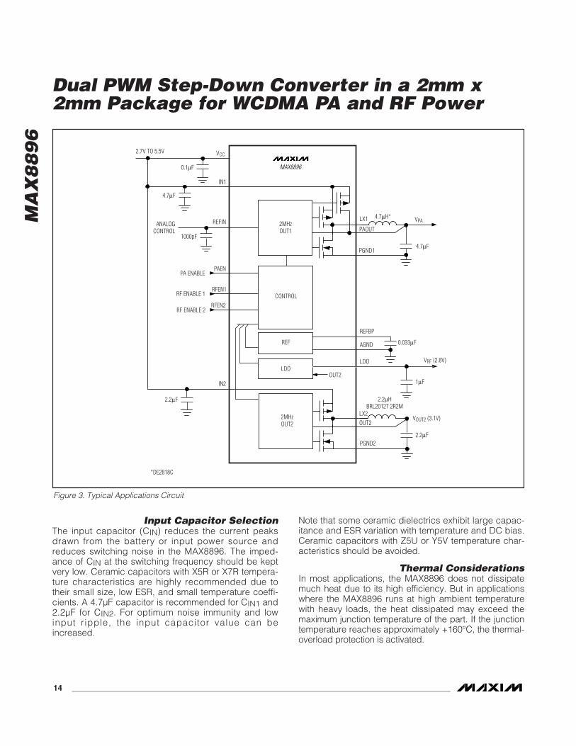
Applications InformationInductor Selection
OUT1 operates with a switching frequency of 2MHz andutilizes a 2.2µH to 4.7µH inductor. OUT2 operates with aswitching frequency of 2MHz and utilizes a 2.2µH induc-tor. This operating frequency allows the use of physicallysmall inductors while maintaining high efficiency.
The OUT1 inductor’s DC current rating only needs tomatch the maximum load of the application becauseOUT1 features zero current overshoot during startup andload transients. For optimum transient response and highefficiency, choose an inductor with DC series resistancein the 50mΩ to 150mΩ range. See Table 1 for suggestedinductors and manufacturers.
Using a larger inductance value reduces the ripple cur-rent, therefore providing higher efficiency at light load.
Output Capacitor SelectionFor OUT1 and OUT2, the output capacitor keeps theoutput voltage ripple small and ensures regulation loopstability. COUT must have low impedance at the switch-ing frequency. Ceramic capacitors with X5R or X7Rtemperature characteristics are highly recommendeddue to their small size, low ESR, and small temperaturecoefficients. A 4.7µF capacitor is recommended forCOUT1 and 2.2µF is recommended for COUT2. For opti-mum load-transient performance and very low outputripple, the output capacitor value can be increased.
For the LDO, the minimum output capacitance requiredis dependent on the load currents. For loads lighterthan 10mA, it is sufficient to use a 0.1µF capacitor forstable operation over the full temperature range. Withrated maximum load currents, a minimum of 1µF is rec-ommended. Larger value output capacitors furtherreduce output noise and improve load-transientresponse, stability, and power-supply rejection.
Note that some ceramic dielectrics exhibit large capac-itance and ESR variation with temperature and DC bias.Ceramic capacitors with Z5U or Y5V temperature char-acteristics should be avoided. These regulators areoptimized for ceramic capacitors. Tantalum capacitorsare not recommended.
MA
X8
89
6
Dual PWM Step-Down Converter in a 2mm x2mm Package for WCDMA PA and RF Power
14 ______________________________________________________________________________________
Input Capacitor SelectionThe input capacitor (CIN) reduces the current peaksdrawn from the battery or input power source andreduces switching noise in the MAX8896. The imped-ance of CIN at the switching frequency should be keptvery low. Ceramic capacitors with X5R or X7R tempera-ture characteristics are highly recommended due totheir small size, low ESR, and small temperature coeffi-cients. A 4.7µF capacitor is recommended for CIN1 and2.2µF for CIN2. For optimum noise immunity and lowinput ripple, the input capacitor value can beincreased.
Note that some ceramic dielectrics exhibit large capac-itance and ESR variation with temperature and DC bias.Ceramic capacitors with Z5U or Y5V temperature char-acteristics should be avoided.
Thermal ConsiderationsIn most applications, the MAX8896 does not dissipatemuch heat due to its high efficiency. But in applicationswhere the MAX8896 runs at high ambient temperaturewith heavy loads, the heat dissipated may exceed themaximum junction temperature of the part. If the junctiontemperature reaches approximately +160°C, the thermal-overload protection is activated.
2MHzOUT1
LX1
PGND1
PAOUT
IN1
RFEN1
REFIN
REF
REFBP
*DE2818C
AGND
LDO
IN2
PAEN
CONTROL
PA ENABLE
RF ENABLE 1
ANALOGCONTROL
2MHzOUT2
LX2
PGND2
RFEN2
OUT2
1000pF
RF ENABLE 2
2.7V TO 5.5V
0.1µF
VCC
4.7µF
0.033µF
2.2µHBRL2012T 2R2M
2.2µF
VRF (2.8V)
2.2µF
4.7µH* VPA
4.7µF
MAX8896
VOUT2 (3.1V)
LDOOUT2
1µF
Figure 3. Typical Applications Circuit

MA
X8
89
6
Dual PWM Step-Down Converter in a 2mm x2mm Package for WCDMA PA and RF Power
______________________________________________________________________________________ 15
The MAX8896 maximum power dissipation depends onthe thermal resistance of the IC package and circuitboard, the temperature difference between the diejunction and ambient air, and the rate of airflow. Thepower dissipated in the device is:
PD = POUT1 x (1/ηOUT1 - 1) + POUT2 x (1/ηOUT2 - 1) +ILDO x (VOUT2 - VLDO)
where η is the efficiency of the step-down converter andPOUT_ is the output power of the step-down converter.The maximum allowed power dissipation is:
PMAX = (TJMAX - TA)/θJA
where (TJMAX - TA) is the temperature differencebetween the MAX8896 die junction and the surroundingair, θJA is the thermal resistance of the junction throughthe PCB, copper traces, and other materials to the sur-rounding air.
PCB LayoutHigh switching frequencies and relatively large peakcurrents make the PCB layout a very important part ofdesign. Good design minimizes excessive EMI on thefeedback paths and voltage gradients in the groundplane, resulting in a stable and well regulated output.Connect CIN1 close to IN1 and PGND1 and connectCIN2 close to IN2 and PGND2. Connect the inductorand output capacitor as close as possible to the IC andkeep their traces short, direct, and wide. Keep noisytraces, such as the LX node, as short as possible. Referto the MAX8896EVKIT for an example layout.

MA
X8
89
6
Dual PWM Step-Down Converter in a 2mm x2mm Package for WCDMA PA and RF Power
16 ______________________________________________________________________________________
MANUFACTURER SERIESINDUCTANCE
(µH)ESR(Ω)
CURRENT RATING (mA) DIMENSIONS
CB2016T1.02.2
0.090.13
600510
2.0mm x 1.6mm x 1.8mm= 5.8mm3
CB2518T2.24.7
0.090.13
510340
2.5mm x 1.8mm x 2.0mm= 9mm3
BRL2012T 2.2 0.30 5502.0mm x 1.25mm x 1.0mm
= 2.5mm3
Taiyo Yuden
CKP2520 2.2 0.09 13002.5mm x 2.0mm x 1.0mm
= 5mm3
MIPF25201.01.52.2
0.050.070.08
150015001300
2.5mm x 2.0mm x 1.0mm= 5mm3
FDK
MIPF2016 2.2 0.11 11002.0mm x 1.6mm x 1.0mm
= 3.2mm3
Murata LQH32C_531.02.2
0.060.10
1000790
3.2mm x 2.5mm x 1.7mm= 14mm3
D3010FB 1.0 0.20 11703.0mm x 3.0mm x 1.0mm
= 9mm3
D2812C1.22.2
0.090.15
860640
3.0mm x 3.0mm x 1.2mm= 11mm3
D310F1.52.2
0.130.17
12301080
3.6mm x 3.6mm x 1.0mm= 13mm3
D312C1.52.2
0.100.12
12901140
3.6mm x 3.6mm x 1.2mm= 16mm3
TOKO
DE2818C 4.7 72 9503.2mm x 3.0mm x 1.8mm
= 17.3mm3
CDRH2D091.21.52.2
0.080.090.12
590520440
3.0mm x 3.0mm x 1.0mm= 9mm3
Sumida
CDRH2D111.52.23.3
0.050.080.10
680580450
3.2mm x 3.2mm x 1.2mm= 12mm3
LPO33101.01.52.2
0.070.100.13
160014001100
3.3mm x 3.3mm x 1.0mm= 11mm3
Coilcraft
XPL2010 4.7 0.284 7401.9mm x 2.0mm x 1.0mm
= 3.8mm3
ELC3FN1.02.2
0.080.12
14001000
3.2mm x 3.2mm x 1.2mm= 12mm3
Panasonic
ELL3GM1.02.2
0.070.10
14001100
3.2mm x 3.2mm x 1.5mm= 15mm3
Table 1. Suggested Inductors

MA
X8
89
6
Dual PWM Step-Down Converter in a 2mm x2mm Package for WCDMA PA and RF Power
16-BUMP UCSP
A
B
C
1 2 3 4MAX8896
D
TOP VIEW(BUMPS ON BOTTOM)
D4D3
C4C3
B4B3
A4A3
D2D1
C2C1
B2B1
A2A1
PGND1REFINAGNDREFBP
LX1RFEN2PAENLDO
IN1VCCRFEN1OUT2
PAOUTIN2LX2PGND2
Pin Configuration
Package InformationFor the latest package outline information and land patterns, goto www.maxim-ic.com/packages.
PACKAGE TYPE PACKAGE CODE DOCUMENT NO.
16 UCSP R162A2+1 21-0226
Maxim cannot assume responsibility for use of any circuitry other than circuitry entirely embodied in a Maxim product. No circuit patent licenses areimplied. Maxim reserves the right to change the circuitry and specifications without notice at any time.
Maxim Integrated Products, 120 San Gabriel Drive, Sunnyvale, CA 94086 408-737-7600 ____________________ 17
© 2009 Maxim Integrated Products Maxim is a registered trademark of Maxim Integrated Products, Inc.
Chip InformationPROCESS: BiCMOS