Embed Size (px)
Citation preview

18-447
Computer Architecture
Lecture 5: ISA Wrap-Up and
Single-Cycle Microarchitectures
Prof. Onur Mutlu
Carnegie Mellon University
Spring 2012, 1/25/2012

Homework 0
Was due Wednesday!
34 received
2

Reminder: Homeworks for Next Two Weeks
Homework 1
Due Monday Jan 28, right before lecture
Turn in via AFS (hand-in directories)
MIPS warmup, ISA concepts, basic performance evaluation
Homework 2
Will be assigned next week. Stay tuned…
3

Reminder: Lab Assignment 1
Due next Friday (Feb 1), at the end of Friday lab
A functional C-level simulator for a subset of the MIPS ISA
Study the MIPS ISA Tutorial
TAs will cover this in Lab Sessions this week
4

A Note on Lab and Homework Dates
Intended dates are on your syllabus
http://www.ece.cmu.edu/~ece447/s13/lib/exe/fetch.php?media=syllabus-18-447-mutlu-s13.pdf
We will try to stick to them.
Last year’s website can provide you a good lookahead into what is coming…
http://www.ece.cmu.edu/~ece447/s12/doku.php
http://www.ece.cmu.edu/~ece447/s12/doku.php?id=wiki:lectures
5

Readings for Next Lecture
P&P, Revised Appendix C
Microarchitecture of the LC-3b
Appendix A (LC-3b ISA) will be useful in following this
P&H, Appendix D
Mapping Control to Hardware
Optional
Maurice Wilkes, “The Best Way to Design an Automatic Calculating Machine,” Manchester Univ. Computer Inaugural Conf., 1951.
6

Review of Last Lecture: ISA Tradeoffs
Complex vs. simple instructions: concept of semantic gap
Use of translation to change the tradeoffs
Fixed vs. variable length, uniform vs. non-uniform decode
Number of registers
What is the benefit of translating complex instructions to “simple instructions” before executing them?
In hardware (a la Intel, AMD)?
In software (a la Transmeta)?
Which ISA is easier to extend: fixed length or variable length?
How can you have a variable length, uniform decode ISA?
7

Review: x86 vs. Alpha Instruction Formats
x86:
Alpha:
8

Review: ISA-level Tradeoffs: Number of Registers
Affects:
Number of bits used for encoding register address
Number of values kept in fast storage (register file)
(uarch) Size, access time, power consumption of register file
Large number of registers:
+ Enables better register allocation (and optimizations) by compiler fewer saves/restores
-- Larger instruction size
-- Larger register file size
9

ISA-level Tradeoffs: Addressing Modes
Addressing mode specifies how to obtain an operand of an instruction
Register
Immediate
Memory (displacement, register indirect, indexed, absolute, memory indirect, autoincrement, autodecrement, …)
More modes:
+ help better support programming constructs (arrays, pointer-based accesses)
-- make it harder for the architect to design
-- too many choices for the compiler?
Many ways to do the same thing complicates compiler design
Wulf, “Compilers and Computer Architecture,” IEEE Computer 1981
10

x86 vs. Alpha Instruction Formats
x86:
Alpha:
11

12
x86
register
absolute
register
indirect
register +
displacement

x86
13
indexed
(base +
index)
scaled
(base +
index*4)
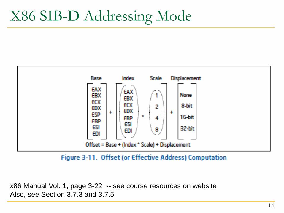
X86 SIB-D Addressing Mode
14
x86 Manual Vol. 1, page 3-22 -- see course resources on website
Also, see Section 3.7.3 and 3.7.5

X86 Manual: Suggested Uses of Addressing Modes
15
x86 Manual Vol. 1, page 3-22 -- see course resources on website
Also, see Section 3.7.3 and 3.7.5

X86 Manual: Suggested Uses of Addressing Modes
16
x86 Manual Vol. 1, page 3-22 -- see course resources on website
Also, see Section 3.7.3 and 3.7.5

Other Example ISA-level Tradeoffs
Condition codes vs. not
VLIW vs. single instruction
Precise vs. imprecise exceptions
Virtual memory vs. not
Unaligned access vs. not
Hardware interlocks vs. software-guaranteed interlocking
Software vs. hardware managed page fault handling
Cache coherence (hardware vs. software)
…
17

Back to Programmer vs. (Micro)architect
Many ISA features designed to aid programmers
But, complicate the hardware designer’s job
Virtual memory
vs. overlay programming
Should the programmer be concerned about the size of code blocks fitting physical memory?
Addressing modes
Unaligned memory access
Compile/programmer needs to align data
18

MIPS: Aligned Access
LW/SW alignment restriction: 4-byte word-alignment
not designed to fetch memory bytes not within a word boundary
not designed to rotate unaligned bytes into registers
Provide separate opcodes for the “infrequent” case
LWL/LWR is slower
Note LWL and LWR still fetch within word boundary
19
byte-3 byte-2 byte-1 byte-0
byte-7 byte-6 byte-5 byte-4
MSB LSB
A B C D
byte-6 byte-5 byte-4 D
byte-6 byte-5 byte-4 byte-3
LWL rd 6(r0)
LWR rd 3(r0)

X86: Unaligned Access
LD/ST instructions automatically align data that spans a “word” boundary
Programmer/compiler does not need to worry about where data is stored (whether or not in a word-aligned location)
20

X86: Unaligned Access
21

Aligned vs. Unaligned Access
Pros of having no restrictions on alignment
Cons of having no restrictions on alignment
Filling in the above: an exercise for you…
22

Implementing the ISA:
Microarchitecture Basics
23

How Does a Machine Process Instructions?
What does processing an instruction mean?
Remember the von Neumann model
A = Architectural (programmer visible) state before an instruction is processed
Process instruction
A’ = Architectural (programmer visible) state after an instruction is processed
Processing an instruction: Transforming A to A’ according to the ISA specification of the instruction
24

The “Process instruction” Step
ISA specifies abstractly what A’ should be, given an instruction and A
It defines an abstract finite state machine where
State = programmer-visible state
Next-state logic = instruction execution specification
From ISA point of view, there are no “intermediate states” between A and A’ during instruction execution
One state transition per instruction
Microarchitecture implements how A is transformed to A’
There are many choices in implementation
We can have programmer-invisible state to optimize the speed of instruction execution: multiple state transitions per instruction
Choice 1: A A’ (transform A to A’ in a single clock cycle)
Choice 2: A A+MS1 A+MS2 A+MS3 A’ (take multiple clock
cycles to transform A to A’)
25

A Very Basic Instruction Processing Engine
Each instruction takes a single clock cycle to execute
Only combinational logic is used to implement instruction execution
No intermediate, programmer-invisible state updates
A = Architectural (programmer visible) state
at the beginning of a clock cycle
Process instruction in one clock cycle
A’ = Architectural (programmer visible) state
at the end of a clock cycle
26

A Very Basic Instruction Processing Engine
Single-cycle machine
What is the clock cycle time determined by?
What is the critical path of the combinational logic determined by?
27
ANext A Sequential Logic (State)
Combinational Logic

Remember: Programmer Visible (Architectural) State
28
M[0]
M[1]
M[2]
M[3]
M[4]
M[N-1] Memory
array of storage locations indexed by an address
Program Counter memory address of the current instruction
Registers
- given special names in the ISA (as opposed to addresses) - general vs. special purpose
Instructions (and programs) specify how to transform the values of programmer visible state

Single-cycle vs. Multi-cycle Machines
Single-cycle machines
Each instruction takes a single clock cycle
All state updates made at the end of an instruction’s execution
Big disadvantage: The slowest instruction determines cycle time
long clock cycle time
Multi-cycle machines
Instruction processing broken into multiple cycles/stages
State updates can be made during an instruction’s execution
Architectural state updates made only at the end of an instruction’s execution
Advantage over single-cycle: The slowest “stage” determines cycle time
Both single-cycle and multi-cycle machines literally follow the von Neumann model at the microarchitecture level
29

Instruction Processing “Cycle”
Instructions are processed under the direction of a “control unit” step by step.
Instruction cycle: Sequence of steps to process an instruction
Fundamentally, there are six phases:
Fetch
Decode
Evaluate Address
Fetch Operands
Execute
Store Result
Not all instructions require all six stages (see P&P Ch. 4) 30

Instruction Processing “Cycle” vs. Machine Clock Cycle
Single-cycle machine:
All six phases of the instruction processing cycle take a single machine clock cycle to complete
Multi-cycle machine:
All six phases of the instruction processing cycle can take multiple machine clock cycles to complete
In fact, each phase can take multiple clock cycles to complete
31

Instruction Processing Viewed Another Way Instructions transform Data (AS) to Data’ (AS’)
This transformation is done by functional units Units that “operate” on data
These units need to be told what to do to the data
An instruction processing engine consists of two components
Datapath: Consists of hardware elements that deal with and transform data signals
functional units that operate on data
hardware structures (e.g. wires and muxes) that enable the flow of data into the functional units and registers
storage units that store data (e.g., registers)
Control logic: Consists of hardware elements that determine control signals, i.e., signals that specify what the datapath elements should do to the data
32
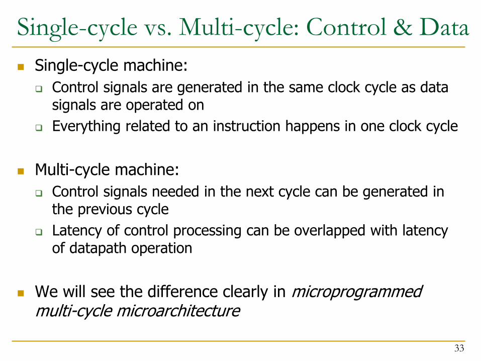
Single-cycle vs. Multi-cycle: Control & Data
Single-cycle machine:
Control signals are generated in the same clock cycle as data signals are operated on
Everything related to an instruction happens in one clock cycle
Multi-cycle machine:
Control signals needed in the next cycle can be generated in the previous cycle
Latency of control processing can be overlapped with latency of datapath operation
We will see the difference clearly in microprogrammed multi-cycle microarchitecture
33

Many Ways of Datapath and Control Design
There are many ways of designing the data path and control logic
Single-cycle, multi-cycle, pipelined datapath and control
Single-bus vs. multi-bus datapaths
See your homework 2 question
Hardwired/combinational vs. microcoded/microprogrammed control
Control signals generated by combinational logic versus
Control signals stored in a memory structure
Control signals and structure depend on the datapath design
34

Flash-Forward: Performance Analysis
Execution time of an instruction
{CPI} x {clock cycle time}
Execution time of a program
Sum over all instructions [{CPI} x {clock cycle time}]
{# of instructions} x {Average CPI} x {clock cycle time}
Single cycle microarchitecture performance
CPI = 1
Clock cycle time = long
Multi-cycle microarchitecture performance
CPI = different for each instruction
Average CPI hopefully small
Clock cycle time = short 35
Now, we have
two degrees of freedom
to optimize independently

A Single-Cycle Microarchitecture
A Closer Look
36

Remember…
Single-cycle machine
37
ASNext AS Sequential Logic (State)
Combinational Logic

Let’s Start with the State Elements
Data and control inputs
38
P C
In s tru c tion
m e m o ry
In s tru c tio n
a d d res s
In s tru c tio n
a . In s tru c tio n m e m o ry b . P ro g ra m c o u n te r
A d d S u m
c . A d d e r
P C
In s tru c tio n
m e m o ry
In s tru c tio n
a d d re s s
In s tru c tio n
a . In s t ru c tio n m e m o ry b . P ro g ram c o u n te r
A d d S um
c . A d de r
1 6 3 2S ig n
e x te n d
b . S ig n -e x te n s io n un it
M e m R e a d
M e m W rite
D a ta
m e m o ryW rite
d a ta
R e a d
d a ta
a . D a ta m e m o ry u n it
A d d re s s
A LU co n tro l
R eg W rite
R eg is te rs
W rite
re g is te r
R e ad
d a ta 1
R e ad
d a ta 2
R e ad
re g is te r 1
R e ad
re g is te r 2
W rite
d a ta
A L U
re su lt
A L U
D a ta
D a ta
R eg is te r
nu m be rs
a . R e g is te rs b . A L U
Z e ro
5
5
5 3
**Based on original figure from [P&H CO&D, COPYRIGHT 2004 Elsevier. ALL RIGHTS RESERVED.]
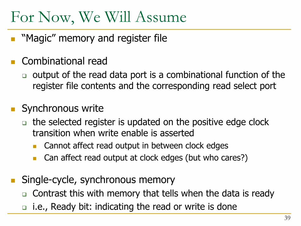
For Now, We Will Assume
“Magic” memory and register file
Combinational read
output of the read data port is a combinational function of the register file contents and the corresponding read select port
Synchronous write
the selected register is updated on the positive edge clock transition when write enable is asserted
Cannot affect read output in between clock edges
Can affect read output at clock edges (but who cares?)
Single-cycle, synchronous memory
Contrast this with memory that tells when the data is ready
i.e., Ready bit: indicating the read or write is done
39

Instruction Processing
5 generic steps (P&H)
Instruction fetch (IF)
Instruction decode and register operand fetch (ID/RF)
Execute/Evaluate memory address (EX/AG)
Memory operand fetch (MEM)
Store/writeback result (WB)
40
R e g is te rs
R e g is te r #
D a ta
R e g is te r #
D a ta
m e m ory
A d dre ss
D ata
R e g is te r #
P C In s tru c tio n A L U
In s tru c tion
m e m ory
A d d re ss
IF
ID/RF EX/AG
MEM
WB
**Based on original figure from [P&H CO&D, COPYRIGHT 2004 Elsevier. ALL RIGHTS RESERVED.]

What Is To Come: The Full Datapath
41
S h ift
le ft 2
P C
In s truc tio n
m e m ory
R e a d
ad d re ss
In struc tio n
[3 1– 0]
D ata
m e m o ry
R e a d
d ata
W rite
d ata
R eg is te rs
W rite
re gis te r
W rite
da ta
R e a d
da ta 1
R e a d
da ta 2
R ea d
re gis te r 1
R ea d
re gis te r 2
Ins truc tio n [1 5– 1 1]
Ins truc tio n [2 0– 1 6]
Ins truc tio n [2 5– 2 1]
A d d
A L U
re su lt
Z e ro
In stru ction [5– 0 ]
M e m to R eg
A L U O p
M e m W rite
R e g W rite
M e m R e a d
B ra n ch
Ju m p
R e g D st
A L U S rc
Ins truc tio n [3 1– 2 6]
4
M
u
x
Ins tru ctio n [2 5– 0 ] Ju m p a d dres s [31– 0]
P C +4 [31– 2 8 ]
S ig n
e xte n d
1 6 3 2Ins truc tio n [1 5– 0 ]
1
M
u
x
1
0
M
u
x
0
1
M
u
x
0
1
A L U
co n tro l
C o ntro l
A d dA LU
re su lt
M
u
x
0
1 0
A L U
S h ift
left 226 2 8
A d d re ss
PCSrc2=Br Taken
PCSrc1=Jump
ALU operation
bcond
**Based on original figure from [P&H CO&D, COPYRIGHT 2004 Elsevier. ALL RIGHTS RESERVED.] JAL, JR, JALR omitted

Single-Cycle Datapath for
Arithmetic and Logical Instructions
42

R-Type ALU Instructions
Assembly (e.g., register-register signed addition)
ADD rdreg rsreg rtreg
Machine encoding
Semantics
if MEM[PC] == ADD rd rs rt
GPR[rd] GPR[rs] + GPR[rt]
PC PC + 4
43
0 6-bit
rs 5-bit
rt 5-bit
R-type rd 5-bit
0 5-bit
ADD 6-bit

ALU Datapath
44
P C
Ins tru c tio n
m e m ory
R ea d
ad d re ss
Ins tru c t io n
4
A dd
In s truc tio nR e g is te rs
W rite
re g is te r
R ea d
da ta 1
R ea d
da ta 2
R e ad
re g is te r 1
R e ad
re g is te r 2
W rite
d a ta
A L U
res u lt
A L U
Z e ro
R e gW rite
A LU op e ra tion3
1
15:11
20:16
25:21
**Based on original figure from [P&H CO&D, COPYRIGHT 2004 Elsevier. ALL RIGHTS RESERVED.]
if MEM[PC] == ADD rd rs rt GPR[rd] GPR[rs] + GPR[rt] PC PC + 4
Combinational state update logic
IF ID EX MEM WB
**Based on original figure from [P&H CO&D, COPYRIGHT 2004 Elsevier. ALL RIGHTS RESERVED.]

I-Type ALU Instructions
Assembly (e.g., register-immediate signed additions)
ADDI rtreg rsreg immediate16
Machine encoding
Semantics
if MEM[PC] == ADDI rt rs immediate
GPR[rt] GPR[rs] + sign-extend (immediate)
PC PC + 4
45
ADDI 6-bit
rs 5-bit
rt 5-bit
immediate 16-bit
I-type

Datapath for R and I-Type ALU Insts.
46
P C
Ins tru c tio n
m e m ory
R ea d
ad d re ss
Ins tru c t io n
4
A dd
In s tru c tio n
1 6 3 2
R eg is te rsW rite
reg is te r
R e a d
d a ta 1
R e a d
d a ta 2
R e a d
reg is te r 1
R e a d
reg is te r 2
D a ta
m e m oryW rite
d a ta
R ea d
da ta
W rite
d a ta
S ign
e x ten d
A LU
re s u lt
Z e ro
A L U
A d d res s
M e m R e a d
M e m W rite
R e g W rite
A L U op e ra tio n3
1 ALUSrc
isItype
RegDest
isItype
15:11
20:16
25:21
**Based on original figure from [P&H CO&D, COPYRIGHT 2004 Elsevier. ALL RIGHTS RESERVED.]
if MEM[PC] == ADDI rt rs immediate GPR[rt] GPR[rs] + sign-extend (immediate) PC PC + 4
Combinational state update logic
IF ID EX MEM WB

Single-Cycle Datapath for
Data Movement Instructions
47

Load Instructions
Assembly (e.g., load 4-byte word)
LW rtreg offset16 (basereg)
Machine encoding
Semantics
if MEM[PC]==LW rt offset16 (base)
EA = sign-extend(offset) + GPR[base]
GPR[rt] MEM[ translate(EA) ]
PC PC + 4
48
LW 6-bit
base 5-bit
rt 5-bit
offset 16-bit
I-type

LW Datapath
49
P C
Ins tru c tio n
m e m ory
R ea d
ad d re ss
Ins tru c t io n
4
A dd
In s tru c tio n
1 6 3 2
R eg is te rsW rite
reg is te r
R e a d
d a ta 1
R e a d
d a ta 2
R e a d
reg is te r 1
R e a d
reg is te r 2
D a ta
m e m oryW rite
d a ta
R ea d
da ta
W rite
d a ta
S ign
e x ten d
A LU
re s u lt
Z e ro
A L U
A d d res s
M e m R e a d
M e m W rite
R e g W rite
A L U op e ra tio n3
ALUSrc
if MEM[PC]==LW rt offset16 (base) EA = sign-extend(offset) + GPR[base] GPR[rt] MEM[ translate(EA) ] PC PC + 4
Combinational state update logic
IF ID EX MEM WB
1 6 3 2S ig n
e x te n d
b . S ig n -e x te n s io n un it
M e m R e a d
M e m W rite
D a ta
m e m o ryW rite
d a ta
R e a d
d a ta
a . D a ta m e m o ry u n it
A d d re s s
1
add
isItype
RegDest isItype
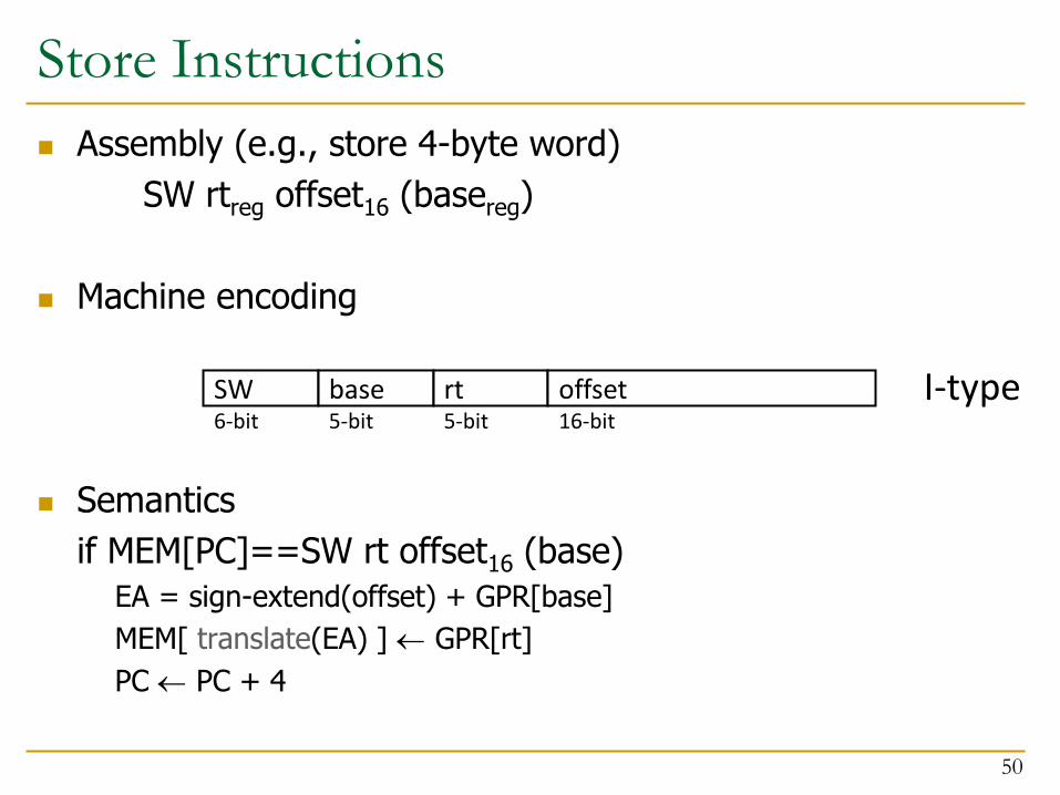
Store Instructions
Assembly (e.g., store 4-byte word)
SW rtreg offset16 (basereg)
Machine encoding
Semantics
if MEM[PC]==SW rt offset16 (base)
EA = sign-extend(offset) + GPR[base]
MEM[ translate(EA) ] GPR[rt]
PC PC + 4
50
SW 6-bit
base 5-bit
rt 5-bit
offset 16-bit
I-type

SW Datapath
51
P C
Ins tru c tio n
m e m ory
R ea d
ad d re ss
Ins tru c t io n
4
A dd
In s tru c tio n
1 6 3 2
R eg is te rsW rite
reg is te r
R e a d
d a ta 1
R e a d
d a ta 2
R e a d
reg is te r 1
R e a d
reg is te r 2
D a ta
m e m oryW rite
d a ta
R ea d
da ta
W rite
d a ta
S ign
e x ten d
A LU
re s u lt
Z e ro
A L U
A d d res s
M e m R e a d
M e m W rite
R e g W rite
A L U op e ra tio n3
if MEM[PC]==SW rt offset16 (base) EA = sign-extend(offset) + GPR[base] MEM[ translate(EA) ] GPR[rt] PC PC + 4
Combinational state update logic
IF ID EX MEM WB
1 6 3 2S ig n
e x te n d
b . S ig n -e x te n s io n un it
M e m R e a d
M e m W rite
D a ta
m e m o ryW rite
d a ta
R e a d
d a ta
a . D a ta m e m o ry u n it
A d d re s s
0
add
ALUSrc
isItype
RegDest isItype

Load-Store Datapath
52
P C
Ins tru c tio n
m e m ory
R ea d
ad d re ss
Ins tru c t io n
4
A dd
In s tru c tio n
1 6 3 2
R eg is te rsW rite
reg is te r
R e a d
d a ta 1
R e a d
d a ta 2
R e a d
reg is te r 1
R e a d
reg is te r 2
D a ta
m e m oryW rite
d a ta
R ea d
da ta
W rite
d a ta
S ign
e x ten d
A LU
re s u lt
Z e ro
A L U
A d d res s
M e m R e a d
M e m W rite
R e g W rite
A L U op e ra tio n3
!isStore
add isStore
isLoad
ALUSrc
isItype
RegDest
isItype
**Based on original figure from [P&H CO&D, COPYRIGHT 2004 Elsevier. ALL RIGHTS RESERVED.]

Datapath for Non-Control-Flow Insts.
53
P C
Ins tru c tio n
m e m ory
R ea d
ad d re ss
Ins tru c t io n
4
A dd
In s tru c tio n
1 6 3 2
R eg is te rsW rite
reg is te r
R e a d
d a ta 1
R e a d
d a ta 2
R e a d
reg is te r 1
R e a d
reg is te r 2
D a ta
m e m oryW rite
d a ta
R ea d
da ta
W rite
d a ta
S ign
e x ten d
A LU
re s u lt
Z e ro
A L U
A d d res s
M e m R e a d
M e m W rite
R e g W rite
A L U op e ra tio n3
!isStore
isStore
isLoad
ALUSrc
isItype
MemtoReg
isLoad
RegDest
isItype
**Based on original figure from [P&H CO&D, COPYRIGHT 2004 Elsevier. ALL RIGHTS RESERVED.]

Single-Cycle Datapath for
Control Flow Instructions
54

Unconditional Jump Instructions
Assembly
J immediate26
Machine encoding
Semantics
if MEM[PC]==J immediate26
target = { PC[31:28], immediate26, 2’b00 }
PC target
55
J 6-bit
immediate 26-bit
J-type

Unconditional Jump Datapath
56
P C
Ins tru c tio n
m e m ory
R ea d
ad d re ss
Ins tru c t io n
4
A dd
In s tru c tio n
1 6 3 2
R eg is te rsW rite
reg is te r
R e a d
d a ta 1
R e a d
d a ta 2
R e a d
reg is te r 1
R e a d
reg is te r 2
D a ta
m e m oryW rite
d a ta
R ea d
da ta
W rite
d a ta
S ign
e x ten d
A LU
re s u lt
Z e ro
A L U
A d d res s
M e m R e a d
M e m W rite
R e g W rite
A L U op e ra tio n3
ALUSrc
concat
PCSrc
isJ
What about JR, JAL, JALR?
?
**Based on original figure from [P&H CO&D, COPYRIGHT 2004 Elsevier. ALL RIGHTS RESERVED.]
0
X 0
0
X
if MEM[PC]==J immediate26 PC = { PC[31:28], immediate26, 2’b00 }

Conditional Branch Instructions
Assembly (e.g., branch if equal)
BEQ rsreg rtreg immediate16
Machine encoding
Semantics (assuming no branch delay slot)
if MEM[PC]==BEQ rs rt immediate16
target = PC + 4 + sign-extend(immediate) x 4
if GPR[rs]==GPR[rt] then PC target
else PC PC + 4
57
BEQ 6-bit
rs 5-bit
rt 5-bit
immediate 16-bit
I-type

Conditional Branch Datapath (For You to Fix)
58
1 6 32S ig n
e x te n d
Z e roA L U
S u m
S h if t
le ft 2
T o b ra n c h
c o n tro l log ic
B ra n c h ta rg e t
P C + 4 fro m in s t ru c tion d a ta p a th
In s tru c tio n
A d d
R e g is te rs
W rite
re g is te r
R e a d
d a ta 1
R e a d
d a ta 2
R e a d
re g is te r 1
R e a d
re g is te r 2
W rite
d a ta
R e g W rite
A L U op e ra tio n3
P C
Ins tru c tio n
m e m ory
R ea d
ad d re ss
Ins tru c t io n
4
A dd
PCSrc
concat
0
sub
How to uphold the delayed branch semantics?
bcond
**Based on original figure from [P&H CO&D, COPYRIGHT 2004 Elsevier. ALL RIGHTS RESERVED.]
watch out

Putting It All Together
59
S h ift
le ft 2
P C
In s truc tio n
m e m ory
R e a d
ad d re ss
In struc tio n
[3 1– 0]
D ata
m e m o ry
R e a d
d ata
W rite
d ata
R eg is te rs
W rite
re gis te r
W rite
da ta
R e a d
da ta 1
R e a d
da ta 2
R ea d
re gis te r 1
R ea d
re gis te r 2
Ins truc tio n [1 5– 1 1]
Ins truc tio n [2 0– 1 6]
Ins truc tio n [2 5– 2 1]
A d d
A L U
re su lt
Z e ro
In stru ction [5– 0 ]
M e m to R eg
A L U O p
M e m W rite
R e g W rite
M e m R e a d
B ra n ch
Ju m p
R e g D st
A L U S rc
Ins truc tio n [3 1– 2 6]
4
M
u
x
Ins tru ctio n [2 5– 0 ] Ju m p a d dres s [31– 0]
P C +4 [31– 2 8 ]
S ig n
e xte n d
1 6 3 2Ins truc tio n [1 5– 0 ]
1
M
u
x
1
0
M
u
x
0
1
M
u
x
0
1
A L U
co n tro l
C o ntro l
A d dA LU
re su lt
M
u
x
0
1 0
A L U
S h ift
left 226 2 8
A d d re ss
PCSrc2=Br Taken
PCSrc1=Jump
ALU operation
bcond
**Based on original figure from [P&H CO&D, COPYRIGHT 2004 Elsevier. ALL RIGHTS RESERVED.] JAL, JR, JALR omitted

We did not cover the following slides in lecture.
These are for your preparation for the next lecture.

Single-Cycle Control Logic
61

Single-Cycle Hardwired Control
As combinational function of Inst=MEM[PC]
Consider
All R-type and I-type ALU instructions
LW and SW
BEQ, BNE, BLEZ, BGTZ
J, JR, JAL, JALR
62
opcode 6-bit
rs 5-bit
rt 5-bit
immediate 16-bit
I-type
R-type 0 6-bit
rs 5-bit
rt 5-bit
rd 5-bit
shamt 5-bit
funct 6-bit
opcode 6-bit
immediate 26-bit
J-type
0 6 11 16 21 26 31
0 16 21 26 31
0 26 31

Single-Bit Control Signals
63
When De-asserted When asserted Equation
RegDest GPR write select according to rt, i.e., inst[20:16]
GPR write select according to rd, i.e., inst[15:11]
opcode==0
ALUSrc
2nd ALU input from 2nd GPR read port
2nd ALU input from sign-extended 16-bit immediate
(opcode!=0) &&
(opcode!=BEQ) &&
(opcode!=BNE)
MemtoReg Steer ALU result to GPR write port
steer memory load to GPR wr. port
opcode==LW
RegWrite
GPR write disabled GPR write enabled (opcode!=SW) &&
(opcode!=Bxx) &&
(opcode!=J) &&
(opcode!=JR))
JAL and JALR require additional RegDest and MemtoReg options

Single-Bit Control Signals
64
When De-asserted When asserted Equation
MemRead Memory read disabled Memory read port
return load value opcode==LW
MemWrite Memory write disabled Memory write enabled opcode==SW
PCSrc1
According to PCSrc2 next PC is based on 26-bit immediate jump target
(opcode==J) ||
(opcode==JAL)
PCSrc2 next PC = PC + 4 next PC is based on 16-
bit immediate branch target
(opcode==Bxx) &&
“bcond is satisfied”
JR and JALR require additional PCSrc options

ALU Control
case opcode
‘0’ select operation according to funct
‘ALUi’ selection operation according to opcode
‘LW’ select addition
‘SW’ select addition
‘Bxx’ select bcond generation function
__ don’t care
Example ALU operations
ADD, SUB, AND, OR, XOR, NOR, etc.
bcond on equal, not equal, LE zero, GT zero, etc.
65

R-Type ALU
66
S h ift
le ft 2
P C
In s truc tio n
m e m ory
R e a d
ad d re ss
In struc tio n
[3 1– 0]
D ata
m e m o ry
R e a d
d ata
W rite
d ata
R eg is te rs
W rite
re gis te r
W rite
da ta
R e a d
da ta 1
R e a d
da ta 2
R ea d
re gis te r 1
R ea d
re gis te r 2
Ins truc tio n [1 5– 1 1]
Ins truc tio n [2 0– 1 6]
Ins truc tio n [2 5– 2 1]
A d d
A L U
re su lt
Z e ro
In stru ction [5– 0 ]
M e m to R eg
A L U O p
M e m W rite
R e g W rite
M e m R e a d
B ra n ch
Ju m p
R e g D st
A L U S rc
Ins truc tio n [3 1– 2 6]
4
M
u
x
Ins tru ctio n [2 5– 0 ] Ju m p a d dres s [31– 0]
P C +4 [31– 2 8 ]
S ig n
e xte n d
1 6 3 2Ins truc tio n [1 5– 0 ]
1
M
u
x
1
0
M
u
x
0
1
M
u
x
0
1
A L U
co n tro l
C o ntro l
A d dA LU
re su lt
M
u
x
0
1 0
A L U
S h ift
left 226 2 8
A d d re ss
PCSrc2=Br Taken
PCSrc1=Jump
ALU operation
bcond
**Based on original figure from [P&H CO&D, COPYRIGHT 2004 Elsevier. ALL RIGHTS RESERVED.]
1 0
0 funct

I-Type ALU
67
S h ift
le ft 2
P C
In s truc tio n
m e m ory
R e a d
ad d re ss
In struc tio n
[3 1– 0]
D ata
m e m o ry
R e a d
d ata
W rite
d ata
R eg is te rs
W rite
re gis te r
W rite
da ta
R e a d
da ta 1
R e a d
da ta 2
R ea d
re gis te r 1
R ea d
re gis te r 2
Ins truc tio n [1 5– 1 1]
Ins truc tio n [2 0– 1 6]
Ins truc tio n [2 5– 2 1]
A d d
A L U
re su lt
Z e ro
In stru ction [5– 0 ]
M e m to R eg
A L U O p
M e m W rite
R e g W rite
M e m R e a d
B ra n ch
Ju m p
R e g D st
A L U S rc
Ins truc tio n [3 1– 2 6]
4
M
u
x
Ins tru ctio n [2 5– 0 ] Ju m p a d dres s [31– 0]
P C +4 [31– 2 8 ]
S ig n
e xte n d
1 6 3 2Ins truc tio n [1 5– 0 ]
1
M
u
x
1
0
M
u
x
0
1
M
u
x
0
1
A L U
co n tro l
C o ntro l
A d dA LU
re su lt
M
u
x
0
1 0
A L U
S h ift
left 226 2 8
A d d re ss
PCSrc2=Br Taken
PCSrc1=Jump
ALU operation
1 0
0
bcond
**Based on original figure from [P&H CO&D, COPYRIGHT 2004 Elsevier. ALL RIGHTS RESERVED.]
opcode
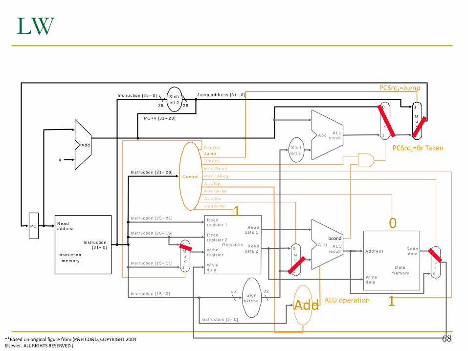
LW
68
S h ift
le ft 2
P C
In s truc tio n
m e m ory
R e a d
ad d re ss
In struc tio n
[3 1– 0]
D ata
m e m o ry
R e a d
d ata
W rite
d ata
R eg is te rs
W rite
re gis te r
W rite
da ta
R e a d
da ta 1
R e a d
da ta 2
R ea d
re gis te r 1
R ea d
re gis te r 2
Ins truc tio n [1 5– 1 1]
Ins truc tio n [2 0– 1 6]
Ins truc tio n [2 5– 2 1]
A d d
A L U
re su lt
Z e ro
In stru ction [5– 0 ]
M e m to R eg
A L U O p
M e m W rite
R e g W rite
M e m R e a d
B ra n ch
Ju m p
R e g D st
A L U S rc
Ins truc tio n [3 1– 2 6]
4
M
u
x
Ins tru ctio n [2 5– 0 ] Ju m p a d dres s [31– 0]
P C +4 [31– 2 8 ]
S ig n
e xte n d
1 6 3 2Ins truc tio n [1 5– 0 ]
1
M
u
x
1
0
M
u
x
0
1
M
u
x
0
1
A L U
co n tro l
C o ntro l
A d dA LU
re su lt
M
u
x
0
1 0
A L U
S h ift
left 226 2 8
A d d re ss
PCSrc2=Br Taken
PCSrc1=Jump
ALU operation
1 0
1
bcond
**Based on original figure from [P&H CO&D, COPYRIGHT 2004 Elsevier. ALL RIGHTS RESERVED.]
Add

SW
69
S h ift
le ft 2
P C
In s truc tio n
m e m ory
R e a d
ad d re ss
In struc tio n
[3 1– 0]
D ata
m e m o ry
R e a d
d ata
W rite
d ata
R eg is te rs
W rite
re gis te r
W rite
da ta
R e a d
da ta 1
R e a d
da ta 2
R ea d
re gis te r 1
R ea d
re gis te r 2
Ins truc tio n [1 5– 1 1]
Ins truc tio n [2 0– 1 6]
Ins truc tio n [2 5– 2 1]
A d d
A L U
re su lt
Z e ro
In stru ction [5– 0 ]
M e m to R eg
A L U O p
M e m W rite
R e g W rite
M e m R e a d
B ra n ch
Ju m p
R e g D st
A L U S rc
Ins truc tio n [3 1– 2 6]
4
M
u
x
Ins tru ctio n [2 5– 0 ] Ju m p a d dres s [31– 0]
P C +4 [31– 2 8 ]
S ig n
e xte n d
1 6 3 2Ins truc tio n [1 5– 0 ]
1
M
u
x
1
0
M
u
x
0
1
M
u
x
0
1
A L U
co n tro l
C o ntro l
A d dA LU
re su lt
M
u
x
0
1 0
A L U
S h ift
left 226 2 8
A d d re ss
PCSrc2=Br Taken
PCSrc1=Jump
ALU operation
0 1
0
* * bcond
**Based on original figure from [P&H CO&D, COPYRIGHT 2004 Elsevier. ALL RIGHTS RESERVED.]
Add

Branch Not Taken
70
S h ift
le ft 2
P C
In s truc tio n
m e m ory
R e a d
ad d re ss
In struc tio n
[3 1– 0]
D ata
m e m o ry
R e a d
d ata
W rite
d ata
R eg is te rs
W rite
re gis te r
W rite
da ta
R e a d
da ta 1
R e a d
da ta 2
R ea d
re gis te r 1
R ea d
re gis te r 2
Ins truc tio n [1 5– 1 1]
Ins truc tio n [2 0– 1 6]
Ins truc tio n [2 5– 2 1]
A d d
A L U
re su lt
Z e ro
In stru ction [5– 0 ]
M e m to R eg
A L U O p
M e m W rite
R e g W rite
M e m R e a d
B ra n ch
Ju m p
R e g D st
A L U S rc
Ins truc tio n [3 1– 2 6]
4
M
u
x
Ins tru ctio n [2 5– 0 ] Ju m p a d dres s [31– 0]
P C +4 [31– 2 8 ]
S ig n
e xte n d
1 6 3 2Ins truc tio n [1 5– 0 ]
1
M
u
x
1
0
M
u
x
0
1
M
u
x
0
1
A L U
co n tro l
C o ntro l
A d dA LU
re su lt
M
u
x
0
1 0
A L U
S h ift
left 226 2 8
A d d re ss
PCSrc2=Br Taken
PCSrc1=Jump
ALU operation
0 0
0
* *
bcond
**Based on original figure from [P&H CO&D, COPYRIGHT 2004 Elsevier. ALL RIGHTS RESERVED.]
bcond

Branch Taken
71
S h ift
le ft 2
P C
In s truc tio n
m e m ory
R e a d
ad d re ss
In struc tio n
[3 1– 0]
D ata
m e m o ry
R e a d
d ata
W rite
d ata
R eg is te rs
W rite
re gis te r
W rite
da ta
R e a d
da ta 1
R e a d
da ta 2
R ea d
re gis te r 1
R ea d
re gis te r 2
Ins truc tio n [1 5– 1 1]
Ins truc tio n [2 0– 1 6]
Ins truc tio n [2 5– 2 1]
A d d
A L U
re su lt
Z e ro
In stru ction [5– 0 ]
M e m to R eg
A L U O p
M e m W rite
R e g W rite
M e m R e a d
B ra n ch
Ju m p
R e g D st
A L U S rc
Ins truc tio n [3 1– 2 6]
4
M
u
x
Ins tru ctio n [2 5– 0 ] Ju m p a d dres s [31– 0]
P C +4 [31– 2 8 ]
S ig n
e xte n d
1 6 3 2Ins truc tio n [1 5– 0 ]
1
M
u
x
1
0
M
u
x
0
1
M
u
x
0
1
A L U
co n tro l
C o ntro l
A d dA LU
re su lt
M
u
x
0
1 0
A L U
S h ift
left 226 2 8
A d d re ss
PCSrc2=Br Taken
PCSrc1=Jump
ALU operation
0 0
0
* *
bcond
**Based on original figure from [P&H CO&D, COPYRIGHT 2004 Elsevier. ALL RIGHTS RESERVED.]
bcond

Jump
72
S h ift
le ft 2
P C
In s truc tio n
m e m ory
R e a d
ad d re ss
In struc tio n
[3 1– 0]
D ata
m e m o ry
R e a d
d ata
W rite
d ata
R eg is te rs
W rite
re gis te r
W rite
da ta
R e a d
da ta 1
R e a d
da ta 2
R ea d
re gis te r 1
R ea d
re gis te r 2
Ins truc tio n [1 5– 1 1]
Ins truc tio n [2 0– 1 6]
Ins truc tio n [2 5– 2 1]
A d d
A L U
re su lt
Z e ro
In stru ction [5– 0 ]
M e m to R eg
A L U O p
M e m W rite
R e g W rite
M e m R e a d
B ra n ch
Ju m p
R e g D st
A L U S rc
Ins truc tio n [3 1– 2 6]
4
M
u
x
Ins tru ctio n [2 5– 0 ] Ju m p a d dres s [31– 0]
P C +4 [31– 2 8 ]
S ig n
e xte n d
1 6 3 2Ins truc tio n [1 5– 0 ]
1
M
u
x
1
0
M
u
x
0
1
M
u
x
0
1
A L U
co n tro l
C o ntro l
A d dA LU
re su lt
M
u
x
0
1 0
A L U
S h ift
left 226 2 8
A d d re ss
PCSrc2=Br Taken
PCSrc1=Jump
ALU operation
0 0
0
* *
*
*
bcond
**Based on original figure from [P&H CO&D, COPYRIGHT 2004 Elsevier. ALL RIGHTS RESERVED.]
*

What is in That Control Box?
Combinational Logic Hardwired Control
Idea: Control signals generated combinationally based on instruction
Sequential Logic Sequential/Microprogrammed Control
Control Store
Idea: A memory structure contains the control signals associated with an instruction
73