Embed Size (px)
Citation preview

"179
THE METAL-ORGANIC CHEMICAL VAPOR DEPOSITION OF Cu(II)-BIS-
HEXAFLUOROACETYLACETONATE ON A TUNGSTEN SUBSTRATE
THESIS
Presented to the Graduate Council of the
University of North Texas in Partial
Fulfillment of the Requirements
For the Degree of
MASTER OF SCIENCE
By
Theresa E. Welton, B.A.
Denton, Texas
May, 1992

Welton, Theresa E., The Metal-Organic Chemical :Vapor Deposition of
Cu(LI)-bishexafluoroacetylacetonate on a Tungsten Substrate. Master of Science
(Chemistry), May, 1993, 32 pp., 12 illustrations, 25 references, 12 titles.
Evidence is reported for the formation of carbon-containing contamination
products at the copper-tungsten (Cu-W) interface during the metal organic
chemical vapor deposition (MOCVD) of copper on tungsten. Cu(II)bishexa-
fluoroacetylacetonate [Cu(hfac) 2] was physisorbed onto lightly oxidized tungsten
(WOW) at 115K, under ultra-high vacuum conditions, and then annealed
sequentially to higher temperatures. Copper reduction was observed'by 320K
Carbonaceous and carbidic contamination of the WO surface was observed, even
after sample warming to 625K in UHV. The results indicate that low temperature
MOCVD of Cu may be possible, but interfacial contamination from the organic
ligand fragmentation is a major concern.

TABLE OF CONTENTS
Page
LIST OF ILLUSTRATIONS
Chapter
I. INTRODUCTION
Background of Chemical Vapor DepositionApplications for Chemical Vapor DepositionMotivation for Using CopperPrevious WorkBackground of X-Ray Photoelectron Spectroscopy
II. EXPERIMENTAL
III. RESULTS AND DISCUSSION
IV. CONCLUSIONS
ENDNOTESREFERENCES
iii
iv
1457
10
15
19
25
2731

LIST OF ILLUSTRATIONS
Page
Figure 1 The Metal Organic Chemical Vapor Deposition ProcessFigure 2 Sputtering TechniqueFigure 3 Interfacial ContaminationFigure 4 Schematic Diagram of a Basic XPSFigure 5 Diagram of the Photoelectric ProcessFigure 6 Diagram of the Auger ProcessFigure 7 Schematic Diagram of the Experimental ChamberFigure 8 Partially Oxidized Tungsten SurfaceFigure 9 The Pre-dose Spectra of (a) W and (b) 0Figure 10 The Post-dose Spectra of (a) W and (b) 0Figure 11 The C Is and Cu 2p Spectra at each stepFigure 12 The Post-anneal Spectra of (a) W and (b) 0
234
111213151620212224
iv

CHAPTER I
INTRODUCTION
Background of Chemical Vapor Deposition
Metal organic chemical vapor deposition (MOCVD) is a technique of thin
film deposition by exposure of the substrate to a vapor of organometallic
molecules (precursors) containing the desired atom (or atoms) for film growth. In
every MOCVD reaction, the following steps must occur: (a) the reacting gaseous
species must be transported to the surface; (b) the species must react at the
surface allowing the nucleation of the film; and (c) the gaseous organic reaction
products must desorb from the surface and be transported away[1]. Essential
issues in all MOCVD processes are the film purity and microstructure, the
deposition rate of the solid film, the deposition uniformity over an extended
surface, and the morphology of the solid film.
A major advantage MOCVD has over other deposition techniques is
enhanced conformal coverage[2] which is of increasing importance with the
continuing shrinkage of microelectronic features. MOCVD is a nondirectional
process that allows the coating or infiltration of objects with intricate shapes or
complex surface topographies. This is an important advantage over line-of-sight
physical vapor deposition or sputter deposition techniques which have difficulties
coating nonplanar items or filling high-aspect feature holes[3].
1
2
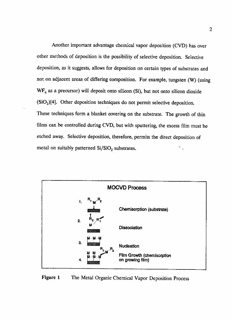
Another important advantage chemical vapor deposition (CVD) has over
other methods of deposition is the possibility of selective deposition. Selective
deposition, as it suggests, allows for deposition on certain types of substrates and
not on adjacent areas of differing composition. For example, tungsten (W) (using
WF6 as a precursor) will deposit onto silicon (Si), but not onto silicon dioxide
(Si02)[4]. Other deposition techniques do not permit selective deposition.
These techniques form a blanket covering on the substrate. The growth of thin
films can be controlled during CVD, but with sputtering, the excess film must be
etched away. Selective deposition, therefore, permits the direct deposition of
metal on suitably patterned Si/Si02 substrates.
MOCVD Process
1.R MR2t iM'R2
Chemisorption (substrate)t
Dissociation
8.R NucleationR ,2 Film Growth (chemisorption
4. on growing film)
FThe Metal Organic Chemical Vapor Deposition ProcessFire I

3
Metal organic chemical vapor deposition is based on the decomposition of
the vapor phase of an organometallic compound with the application of some
form of energy (thermal activation, photon radiation, etc.). The result is the
deposition of a metal, alloy, or compound in the form of a thin film[5]. The
MOCVD process is shown in Figure 1. The properties desired of a precursor for
MOCVD are high vapor pressure, low decomposition temperature, and an
elementary decomposition mechanism that allows clean elimination of the
supporting ligands to form a pure metal deposit.
Figure 2 Sputtering technique
metal
Substrate
metallic film
vacant ar

4
Applications for Chemical Vapor Deposition
Applications of CVD stem from the need for advanced thin film technology
in the semiconductor industry. Because the circuit dimensions continue to
decrease in very large scale integration (VLSI) devices, a method for depositing
conformal films over fine features is desired. Chemical vapor deposition is
superior to sputtering for filling in high aspect holes, and has good step coverage
in small areas[6]. The sputtering technique is not as precise as MOCVD. It
tends to plug up the top of the vias, leaving vacant areas, as shown in Figure 2,
instead of completely filling the holes, as occurs with MOCVD.
Metal (pure)
Contaminant
eSubstrate
Interracial Contamination Induces HighContact Resistance
Figure 3 Interfacial Contamination
5
Interconnect metallization is the patterned thin or thick film metallization
on a semiconductor device which conducts electrical current between various
regions of the device. Multilayer metallization involves one or more device layers
with patterned metallization separated by an insulating layer. Vias are openings
through a semiconductor dielectric that allow essential electrical contact among
active device layers. Standard via-fill geometry is such that even one monolayer
of an insulating contaminant at the metal-substrate interface can lead to
unacceptably high contact resistance. Figure 3 illustrates this problem. This may
occur for metal films with very high bulk purity. The line widths in past
semiconductor devices were several micrometers wide, and the vias'to the silicon
substrate were of similar dimensions. Vias currently in use are of the order of a
single micron, some even narrower. Future devices, however, will have 0.25pm
geometry[7] and shallower junctions, hence the need for focused emphasis on
MOCVD for future device fabrication.
Motivation for Using Copper
Copper is of interest for microelectric metallization due to its high
conductivity and resistance to electromigration[8]. Electromigration is the
electrically induced migration of the atoms in a thin film interconnection. This
migration results in a depletion of metal at the electron source region and an
accumulation of metal at the less negative region of the interconnection[9].

6
The high conductivity and electromigration resistance of copper improve the
reliability of the via and reduce the RC time delay in signal processing. The
deposition of copper from metal organic precursors is often difficult due to the
instability of organocopper compounds and their inclination to form nonvolatile
oligomers and polymers[10]. Cu(hfac) 2 has been used here because it does
not possess these handicaps. Copper does diffuse into silicon, however, and so
must be deposited onto a diffusion barrier for device fabrication.
Because copper reduction is initiated by copper-substrate[11], not
ligand-substrate, bond formation, selective deposition should occur on metals,
metal silicides, or on "open" oxides. All of these possess surfaces with accessible
metal sites at the substrate surface for bond formation. This hypothesis has been
confirmed by experiment[12].
Copper has been shown by Reynolds, et.al.[13] to preferentially deposit
onto metal versus dielectrics, therefore a metal diffusion barrier should be
employed. Because of the deposition selectivity of tungsten onto silicon vs. silicon
dioxide[14], tungsten is an excellent potential source for a diffusion
barrier/substrate with possibilities for the development of a totally selective
tungsten/copper metallization process.
Cu(hfac) 2 is a virtually nontoxic solid with a vapor pressure of about 10
mTorr at room temperature[15]. It is thermally stable at temperatures below
523K and sublimes without decomposition at 343K[16]. Its decomposition
mechanism has been studied by Temple and Reisman[17]. They found that at

7
lower temperatures the dominant metal-ligand decomposition mechanism involves
breaking only the bonds between the metal ion and the organic ligand. The
ligand is volatilized with very little fragmentation. Pure copper films are expected
to result form this particular mechanism. They also report, however, that at
higher temperatures the organic ligand itself begins to undergo a fragmentation.
Because of this ligand fragmentation, the Cu films contain carbon and oxygen
contamination. Therefore, some of the experiments described here were carried
out in the presence of molecular hydrogen to determine the effect of a carrier gas
has on the purity of the copper films.
Previous Work
Many other organometallic precursors have been employed for the CVD of
copper. A few of these are the low molecular weight alkyl copper(I) tri-
alkylphosphine compounds[18], copper(I) tert-butoxide[19], and 1,5-
cyclooctadiene copper(I) hexafluoroacetylacetonate[20]. Pure films have been
deposited with a few of these precursors, but interfacial contamination has yet to
be eliminated.
The CVD of copper has been attempted using several different methods of
deposition. These include, among MOCVD, laser chemical vapor deposition
(LCVD)[21][22], and photochemical deposition using either ultra-violet
(UV) light[23] or low pressure mercury arc lamps[24] as irradiation sources.

8
The CVD of copper on substrates of silicon, silicon oxide, or chromium-
copper seeded silicon wafers using tri-alkyphosphine precursors resulted in
blanket films of copper on all of the substrates above 473K[25]. Deposition on
the silicon and silicon oxide occurred only at temperatures above 473K, but on the
seeded substrate deposition resulted at temperatures as low as 403K. Both carbon
and oxygen contamination were present in all of the films[26]. The deposition
of copper films on silicon dioxide (SiO2) employing Cu(I)-tert-butoxide has
produced films with low carbon contamination (below the Auger detection limit),
but with oxygen contamination clearly present[27], while the use of 1,5-
cyclooctadiene copper(I) hexafluoroacetylacetonate as a precursor resulted in
relatively pure films on Si02 with less than 1.0% oxygen, carbon, or fluorine
contamination observed[28]. The MOCVD of copper on metal, metal silicide,
and pre-patterned TiSi2 , W, Cr, Al and Zr was successful at a substrate
temperature of 623K, but no deposition occurred on SiO, or silicon nitride
(Si3 N4)[29]. Temple and Reisman[30] report the attempted growth of
copper films on silicon and silicon oxide wafers of temperatures from 523-923K
using Cu(hfac)2 as a precursor. Relatively pure copper was deposited on
substrates with temperatures of 613 and 703K, but copper deposition occurring at
703K was contaminated with carbon, oxygen, and fluorine. No copper was
deposited at substrate temperatures of 523, 773, or 923K.
Many materials have been studied as potential diffusion barriers[31].
Little attention has been paid, however, to the copper substrate interface. In via

9
filling, this interface is of considerable importance, since it is possible for a
monolayer of highly resistive material (e.g., organic contamination) to lead to
unacceptable contact resistance, even in films of high bulk purity and low sheet
resistance[32]. As copper surfaces are generally much less reactive towards
oxycarbon species than are, for example W, Ti-W, the potential exists for a
formation of a carbonaceous or carbidic interface even under conditions leading
to formation of a clean Cu film. Thus, one can obtain excellent sheet resistance
and unacceptable contact resistance simultaneously. The interactions between the
copper precursor and the substrate surface are important in determining
selectivity, but they also directly determine the level of contamination at the
copper-substrate interface. This is a critical issue for multilevel interconnect
technology, as the electrons traveling a particular interconnect must all pass
through the copper-substrate interface region.
The previous studies mentioned have demonstrated the potential for
deposition of films of high bulk purity[33] in a selective[34] or non-
selective[35] media. However, these studies have not examined the issue of
contamination of the interface between the copper and the substrate. Kelber,
et.al.[36] examined this carbonaceous contamination while performing copper
MOCVD on aluminum. On partially oxidized aluminum (AlO ), Cu(II)
separation from the ligand and reduction to Cu(O) occurs by room temperature.
The hexafluoroacetylacetonate (hfac) ligand remains associatively adsorbed on the
surface. At higher temperatures decomposition of the organic moiety occurs

10
rather than desorption from the surface. The Cu reduction and nucleation
process is apparently initiated by substrate reaction with the Cu atom, rather than
with the ligand[37]. This is indicated by the observation of unreacted hfac on
the AIOX surface at a temperature where Cu reduction and nucleation has already
occurred[38]. The results of this experiment provide evidence that Cu-
substrate bond formation governs the selectivity of Cu deposition, and that room
temperature deposition is possible if a mechanism for ligand volatilization from
the surface can be developed[39]. The experiments previously reported by
Kelber, et.al. presented the background needed for the studies presented here.
Background of X-Ray Photoelectron Spectroscopy
The analysis of a surface by x-ray photoelectron spectroscopy (XPS) is
achieved by irradiating a sample in a vacuum (pressure below 10'' Torr) with
monoenergetic soft x-rays and analyzing the energy of the electrons emitted.
MgKa or AlKa x-rays are used as the irradiation source. They are provided by
the electron bombardment of Mg or Al targets. For Mg and Al, approximately
half of the x-rays produced by this bombardment are the Ka x-rays. A schematic
diagram of the basic apparatus used in XPS is shown in Figure 4[40].
When a beam of low energy x-rays is used to bombard a sample,
photoelectrons are emitted. This is known as the photoelectron effect. The
observed kinetic energy of the photoelectron is related to its binding energy by

11
Es = hv-Ebining - ( 1)
where Ern is the kinetic energy, lv is the energy of the photon, Eiding is the
binding energy of the atomic orbital from which the electron originated, and O, is
the spectrometer work function which is specific for each instrument[41]. A
diagram of the photoelectric process is shown in Figure 5. Because the inelastic
mean free paths of photoelectrons with kinetic energies below 1.5keV are typically
less than 50 Angstroms (A)[42], the majority of the photoelectrons which have
not been inelastically scattered originates within the surface region. Thus XPS is
a surface, or near-surface sensitive technique.
Figure 4 Schematic Diagram of a Basic XPS
ENERGY ANALYZER
AL X-RAY SOURCE
PHOTON ej ELECTRON ELECTROHSAMPLE OPTICS DETECTOR
ne w iiwis . - y

12
The kinetic energy of the electron emitted defines the type of atom, and its
oxidation state. The number of electrons at this energy is related to the number
density of atoms present. The kinetic energies of core electrons (Fig.5) are
characteristic of the type of atom from which the photoelectron originated[43].
Changes in the chemical bonding environment of that atom (e.g. oxidation state)
induces small changes (0.1 eV - 10 eV)[44] in these characteristic energies -
"chemical shifts." Therefore, XPS is used for both surface elemental analysis and
for analysis of surface chemical bonding environments.
L23or 2 p
Lior 1s
photoelectronphoton
_ Kr or Is
The Photoelectric Process
Figure 5 Diagram of the Photoelectric Process
w ~
- a p I~ %
I
.a.0

13
Auger electrons (from the relaxation of the energetic ions left after
photoemission) are emitted as well as the photoelectrons. The Auger electron
emission occurs about 1014 seconds after the photoelectric emission . In the
Auger process, an outer electron falls into the inner orbital vacancy, and a second
electron is emitted, taking with it the excess energy. A diagram of the Auger
process is shown in Figure 6. The Auger electron's kinetic energy is equal to the
difference between the initial ion's energy and the energy of the doubly-charged
final ion. The Auger electron is independent of the mode of the initial ionization.
pA*l
"'
ifp
Auger electron
L23or 2 p
L1or 1s
Figure 6 Diagram of the Auger Process
-I K or 1sThe Auger Process

14
Therefore, the photoionization typically leads to two emitted electrons, a
photoelectron and an Auger electron[45]. Auger chemical shifts are more
complex due to the multi-electron nature of the process and are therefore used
for element identification rather than chemical state analysis.
The electrons that make up the photoemission spectrum are those
originating from within the first 100 Angstroms or so of the surface. Even though
the ionization takes place in the micrometer range depth, only the electrons from
beneath the top few atomic layers of the solid surface can leave the surface
without losing kinetic energy[46]. The electrons that lose energy before
emerging from the surface make up a broad secondary electron background of the
spectrum.
The photoemission spectrum is commonly displayed as a plot of the
number of electrons emitted per energy interval versus their kinetic or binding
energy. Because each element has its own unique spectrum, and the spectral
peaks produced from a mixture are roughly the sum of the elemental peaks from
the individual constituents, qualitative information about the material can be
established. Quantitative details can be acquired from the peak heights or areas.
The chemical states can be assessed by the exact positions and separations of the
peaks, as well as from certain spectral contours[47]. Statistical methods for
decomposing composite spectra, background subtraction, etc. are well established.
In some circumstances, film thicknesses and adsorbate surface coverage may be
determined from an analysis of the intensity data.

CHAPTER II
EXPERIMENTAL
Experiments were carried out in a stainless steel turbomolecular pumped
ultra-high vacuum chamber equipped for sample heating and cooling with XPS
capability. The base pressure of the chamber was 3 x 10' 0 Torr. The XPS
spectra were recorded using a commercial hemispherical analyzer operated at
Figure 7 Schematic Diagram of the Experimental Chamber
15
Analytical ChamberProcessing Chamber (Se-10 Tonr)(10e-9 Ton)
Sample Introduction 11Chamber
100K - 1300K
TurboPump Turbo
Pump
TurboPump

16
50eV pass energy operated in the constant pass energy mode, and
unrnonochromatized Mg Ka radiation of 300W and 115kV. This is a typical setup
for XPS studies. A schematic diagram of the reaction apparatus is shown in
Figure 7.
A clean tungsten (W) sample was annealed at 600K while exposed to
99.995% pure oxygen gas at a pressure of 104 Torr for a period of ten minutes.
The surface of the W was characterized by XPS referencing the energies of the W
4f72,W 4f512, and 0 Is literature values of Handbook of X-Ray Photoelectron
Spectroscopy[48] in comparison to Colton and Rabelais'[49] work and
Binding Energy (eV)
W~f
II +I
" I" a ... .......... ....1.. ... r
I.. .. I ..I I
11 .9 It A 3.e" are as
Figure 8 Partially oxidized tungsten surface.
Qr...a+. .a ~r+. Dnrran a 1* C71 .a.. ... tat..r... D~.a- q a-*~a 4005catre T
WO.
..w.+..;...... ........ s+ ..... ..". ,...... a ... I +..aa
rTa.
I;
1.
f . n."
T-
............
1
i
I
..... .......
.............
i
..............
ai
w
- - ---
..
Sca l r ator s 1 #K N V twtw& / 11 'a 'fi i' 9e 1.68m x cou tOOtc
17
found to be a partially oxidized W surface (Figure 8) with an oxidation state of
+6. These values also agree with those presented in the Handbook of X-Ray
Photoelectron Spectroscopy[50] for W0 3. No studies were made of film
stoichiometry as a function of depth. Therefore, the oxide is described as WO, in
order to denote a lightly oxidized W surface as might be encountered under
LPCVD conditions (typically above 1 milliTorr total pressure), as opposed to a
uniformly stoichiometric W03 film. The sample temperature was varied between
115K and 600K by a combination of liquid nitrogen cooling and resistive heating.
The sample temperature was monitored with a K-type thermocouple spot-welded
to the back of the tantalum (Ta) sample holder.
The precursor Cu(hfac)2 was obtained through Sandia National
Laboratories in Albuquerque, New Mexico. It was contained in an evacuated
pyrex tube surrounded by a constant temperature water bath. This pyrex tube was
attached to a stainless steel manual leak valve and doser tube leading directing
into the chamber. The path from the pyrex container to the doser tube was kept
as short as possible and maintained at a temperature of 343K during the dosing of
the sample to minimize precursor decomposition.
The W substrate was dosed with the copper precursor at a pressure of 9 x
10' Torr and a temperature of 114K for two minutes. No carrier gas was used
during dosing in order to focus on precursor-substrate interaction. XPS spectra
taken after the dose show a multilayer on the surface consisting of the
undecomposed multilayer, as well as copper. The multilayer was then annealed in

18
UHV to 320K to determine the reaction pathways. At 320K, the copper has been
partially reduced, but the hfac is still present on the surface. The sample was
annealed to 600K. The Cu 2p XPS spectrum (Fig 11) reveals that the copper has
been reduced to pure copper metal, but the organic precursor is still present on
the surface, as seen by the C 1s spectrum.
The experiment was repeated, with the annealing procedures executed in
the presence of H2 to determine the effects of hydrogen on the surface reactions.
The H2 made no impact on the results of the original experiment.
The XPS spectra of the physisorbed multilayer indicated little or no sample
decomposition if the temperature of the gas introduction system was maintained
at 343K, but dosing with the gas introduction system at room temperature resulted
in substatial decomposition.
Software by Peter Sherwood[51] facilitated the deconvolution of the
XPS peaks in the spectra. Each peak has seven parameters associated with it.
These are the peak center, height, width, Gaussian-Lorenuzian mix, constant tail
height, exponential tail slope, and tail mixing ratio.[52] These parameters are
entered into the software, and the curve fitting is obtained. The areas of the
peaks , or intensities, are also provided with this curve synthesis option of the
program.

CHAPTER III
RESULTS AND DISCUSSION
The 0 Is, C is, and Cu 2p pre-dose XPS spectra for this experiment are
shown in Figures 9 and 11. The thicknesses of the films on the surface of the
sample were calculated using equation 1[53], where n1/n 2 is the atom fraction,
I1 and 12 are the intensities of species 1 and 2 respectively, and S, and S2 are the
atomic sensitivity factors. The oxide film thickness was calculated to be 2.8662 A,
or one monolayer.
I'i Sn 1 T= (1)
S2
At 115K, Cu(hfac) 2 was physisorbed onto the WO, surface. The Cu (2p)
XPS spectrum (Fig. 11) shows Cu in the +2 oxidation state. The C (is) spectrum
(Fig. 11) shows hydrocarbons and fluorinated carbon species present. The W
spectrum (Fig. 10) shows mainly the oxide. This is expected because the
deposited overlayer preferentially attenuates the tungsten electrons originates
from the metal substrate. The 0 spectrum displays a shift in the Is peak. This
shift is explained by the influence of the carbonyls from the organic ligand[54].
19

20
;ca 1 kSactoa
5 ; ....... ......~ .......... . M++.. f..
L * a....f~
0$. *.
* 16.71 KCounts/"e
.j ..a....a. ..!a. "f. . t#f. .{{a
I wo1
1. Irr..r....~~
" ...... . ."+a.a4 .....
7I
w; Offset
Binding Energy (eV)
21 . 688 tvneecI"" r r. .a.a r r R a a ar r "aI .aw .+a~r fs rRaR~aar
..fr «"""r«w~s~ raaRra." .rrw sRrrra«f.f.a~r..s t e 000041r"i aat a
.ss." .".rs.....a....
l of t" ." U0.0W W
Scale factor 4.133 K c sac offset 63.1 K counts/sec
* .......... ........... ~....I. I...L .......
i ---..-. .................... ........
"............... .......+
...... I........ ......I....
.5............. ." .. .. .... .... "t .
h3a~e ss~ a.e 932.0 3)0.0 3* 0 Ii 0 s o ns s ao.u
Binding Energy (eV)
Figure 9 The Pre-dose Spectra of (a) W and (b) 0
..
rI .a~yI.
b
'C
'A
.t.!
- - - I -1I I l I Igg g. ol ii M ||| lilllig g g g || w
4 _
IIM I/ Yilw-
-___._Ji
gian III .w
'c -Of tset
#rta.MlJtwa
"i!lwiiiilt .w.
.iwirr"tf !t
" .. r t .. " a. r r
. i t i"" i # w
t.J#1 iJ#w#i
Y Y .! i a Y. i
1

21
a Sca le factor
* .......I.. ......7 ....... ... ........ .
95.0 l93 0 9
S. 355 K counts/sec Offset = 2.Z2EI3,.. 3
.. . . . ...1
.r
.. .r ..re e" .a .a.R aw f .a .ft{r. ai{" t4 Ia."rR
.9 39 >7.6 15.*
Binding Energy (eV)
I Ktconts sec
1 .. . 4 .. 01......r..
"" 1a.1.....
b cl atrim 2.244 IC counts/sec Offset = 16.838 K counts/sec
; .I~
".!..a........9..a.*.s.a .. .. w r. ... .....
. . . . . . . . . . ........ .. .......3 .
.+ .ar" .. ar ...... .. . rr!.r.....
2
.. ... ... 0............".. 0.5 )0.0...6.0.w.. . 's..,.,.,... ...
Figure. 10 .The Post-dose...Spectra".of .(a) .W.and .(b).0
>3.. -)1 .# 2$.0 27.0 23.4
.. . . .. e. .,..+

The Cu (2p) spectrum (Fig. 11) shows that reduction occurs by 320K -
substantially below typical processing temperatures [55]. The C (is) spectra
(Fig. 11) at this temperature indicate that the ligand has begun to react with the
c (1s)WC
650K
320K
115K
22
Cu (2p)
650K
A320K
115K
959 953 947 941 935 929
B.E. (eV)295 291 287 283 279
B.E. (eV)275
Figure 11 XPS of Cu(hfac) 2 physisorbed on WOX and then annealed to varioustemperatures. The C Is spectrum shows carbide formation and other carboncontaminants at 650K.
C
Qt)
C
linl m I.IM EII I I II I . . -.. . , I.w
23
WO, surface. Shifts in the energies of the Cu (2p) photoemission mark the
reduction of the Cu(H) to metallic copper[56].
After the last anneal at 650K - a typical temperature range for copper
deposition - the hfac ligand has reacted to yield both WC (as seen by the intensity
at 283 eV) and other carbon containing species, as seen in Figure 12. The
presence of these species at the WO, surface at elevated temperatures in UHV
indicate that they are strongly chemisorbed to the surface. The metallic W peaks
are now clearly distinguishable from the oxide peaks (Fig. 12), indicating
desorption of the organic ligand, and the formation of a thin film. Some of the
organic moiety was desorbed from the surface, but enough remains to
contaminate the tungsten-copper interface. Even this small amount of interfacial
contamination may cause problems.

24
Scale factor s 9. v rn7a/ eKn
a
30
I
'gire ")r" 'i.* f)0i.! 3 , n3.! n.e 1.0 25.0 -. tn., a.o
Binding Energy (eV)b
Scale Factor 3.688 K counts/sec Offset = 66.988 X counts/sec
S4. . I. ... ..rra .......
". . . . j. .{I.! .. 1al .r.*.srg. .... S« ,..} ............
9- I
- j30., r. r. .." .-.. .. 5 0.-.0 526 -..0 5 12. ---..---*"..-
Figure 12 The Post-anneal Spectra of (a) W and (b) 0
c Offset = 21.9?8Kcounts/sec
. . . . . . . ........ ....r. r...... ........... i.........W4f
.... .. ... jsr tA "s r"a.. .. r . I r aat . A
Iaa e.. .rrr .."A w a" .a"ra~~r.aa1r...."..".......................ar"a..... .a ~ra4 r".. aa fr ...aw
. . . . . . ....... .ir1 .."«,"ar !"r ." ~ .tr r f«. .a 4
MI r
- - . 1 - --......... .... .. T ...
.w...a.....f+"....f f
- - - . . . I .1| IlNa m|
VW o-W4K W6 -%w- - -6 4 %O%& II %wwr b.'
s

CHAPTER IV
CONCLUSIONS
These studies indicate that Cu(ll) reduction and metallic film growth can
occur at room temperature, significantly below standard processing temperatures.
The primary obstacle is the formation of carbide, and carbonaceous
contamination at the copper-tungsten interface. Studies confirm that on a lightly
oxidized surface Cu(hfac) 2 still breaks apart by copper-substrate bond formation.
At 650K the ligand has reacted with the WOE surface to yiel. tungsten
carbide (WC), indicated by the peak at 283 eV[57], as well as other
carbonaceous species. Their presence on the surface at these high temperatures
suggest that they are strongly chemisorbed to the substrate. The appearance of
these carbon-containing species displays evidence that MOCVD may lead to
interfacial contamination which may devastate the via interconnect's effectiveness
by leading to high contact resistance.
The Cu reduction and nucleation process is apparently initiated by
substrate reaction with the Cu atom, rather than with the ligand. This is
demonstrated by the observation by Kelber, et.al.[58] of unreacted hfac on the
oxidized aluminum surface at a temperature where Cu reduction and nucleation
has already taken place. This would also suggest that Cu deposition from
25

26
Cu(hfac) 2 would be selective for metal and metal-silicide substrates - as is
apparently the case[59].
These studies confirm the need for more experimentation to explain the
chemistry that occurs between the precursor and the substrate. The precursor
may react differently with the substrate than with the surtece of the growing film .
Therefore, reactions which occur at the substrate-film interface may be far
different than those which occur during subsequent film growth. This can give
rise to a monolayer of contamination at the substrate-film interface, even for films
with very high bulk purity. Such a monolayer can easily be overlooked in
conventional sputter depth-profiling evaluations. Unfortunately, via-fill geometry
is such that even a monolayer of highly resistive material can lead to contact
resistance that is unacceptable for processing. An intimate knowledge of
precursor-substrate interactions is a necessity.

ENDNOTES
1. Arthur Sherman, Chemical Vapor Deposition for Microelectronics; Principles,Technology, and Applications ( New Jersey: Noyes Publications, 1987), p. 78.
2. B.E. Bent, R.G. Nuzzo, and L.H. Dubois, Journal of the American ChemicalSociety, 111, 1989, p. 1634.
3. M.J. Hampden-Smith, T.T. Kodas, M. Paffett, J.K. Farr, and H.-K. Shin,Chemistry of Materials, 2, 1990, p. 636.
4. R.W. Cheek, J.A. Kelber, J. Fleming, R.D. Lujan, and R.S. Blewer, Tungstenand Other Advanced Metals for ULSI Applications in 1990, Proceedings of the1990 Workshop, ed. by G.C. Smith and R. Blumenthal, Materials ResearchSociety, 1991, p.9 9 .
5. Sherman, p. 96.
6. J.O. Carlsson, Critical Reviews in Solid State and Materials Sciences, Volume16, Issue 3, ed. by J.E. Greene (Boca Raton, Fl.: CRC Press, Inc., 1990), p,161.
7. D. Briggs and M.P. Seah, eds., Practical Surface Analysis, Second Edition,Volume 1, (New York: John Wiley & Sons, 1990,) p. 136.
8. Nobuyoshi Awaya and Yoshinobu Arita, Proceedings of the VLSI Symposium,Kyoto, Japan, 1989, p. 103.
9. Briggs and Seah, p. 223.
10. D.B. Beach, F.K. LeGoues and C.-K. Hu, Chemistry of Materials, 1990, 2, p.216.
11. J.A. Kelber, R.S. Blewer, R.D. Lujan, and G. Gutierrez, Proceedings for the5th Workshop on Tungsten and Other Advanced Metals for VLSI/USLIApplications, Materials Research Society Symposium Proceedings, VLSI V, ed.R.S. Blewer (Pittsburgh, PA; Materials Research Society, 1990), p. 345.
12. N. Awaya and Y. Arita, 1989 Symposium on VLSI Technology: Digest ofTechnical Papers (May 22-25, 1989), Kyoto, Japan, p. 103.
27

28
13. S.K. Reynolds, C.J. Smart, and E.F. Baran, Applied Physical Letters, 59(18), 28October, 1991, p. 2332.
14. R.W. Cheek, J.A. Kelber, J. Fleming, R.D. Lujan, and R.S. Blewer, Tungstenand Other Advanced Metals for ULSI Applications in 1990, Proceedings of the1990 Workshop, ed. by G.C. Smith and R. Blumenthal, Materials ResearchSociety, 1991, p. 99.
15. F.A. Houle, C.T. Jones, T. Baum, C. Pico, and C.A. Kovac, Applied PhysicalLetters, 46(2), 15 January, 1985, p. 204.
16. F.A. Houle, C.T. Jones, T. Baum, C. Pico, and C.A. Kovac, p. 204.
17. D. Temple and A. Reisman, Journal of the Electrochemical Society, Vol. 136,No. 11, November 1989, p. 248.
18. D.B. Beach, F.K. LeGoues and C.-K. Hu, Chemistry of Materials, p. 216.
19. P.M. Jefferies and G.S. Girolami, Chemistry of Materials, 1989, 1, p. 8.
20. S.K. Reynolds, C.J. Smart and E.F. Baran, Applied Physical Letters, 59(18), 28October 1991, p. 2333.
21. C.R. Moylan, T.H. Baum, and C.R. Jones, Applied Physics A, 40, 1986, p. 1.
22. F.A. Houle, C.R. Jones, T. Baum, C. Pico, and C.A. Kovac, Applied PhysicalLetters, p. 204.
23. P.M. George and J.L. Beauchamp, Thin Solid Films, 67, 1980, p. L25.
24. C.R. Jones, F.A. Houle, C.A. Kovac, and T.H. Baum, Applied Physical Letters,46(2), 15 January, 1985, p.97.
25. D.B. Beach, F.K. LeGoues, and C.-K. Hu, p. 216.
26. D.B. Beach, F.K. LeGoues, and C.-K. Hu, p. 216.
27. M.J. Hampden-Smith, T.T. Kodas, M. Paffett, J.K. Farr, and H.-K. Shin,Chemistry of Materials, 1990, 2, p. 636.
28. S.K. Reynolds, C.J. Smart, and E.F. Baran, p. 2332.
29. Nobuyoshi Awaya and Yoshinobu Arita, p103.
30. D. Temple and A. Reisman, p. 249.

29
31. S.P. Murada, Proceedings of the 1990 Workshop on Tungsten and OtherAdvanced Metals for ULSI Applications, (Pennsylvania: Materials ResearchSociety, 1990,) pp. 179-180.
32. J.A. Kelber, R.S. Blewer, R.D. Lujan and G. Gutierrez, Proceedings of the1989 Workshop on Tungsten and Other Metals for Advanced VLSI/ULSIApplications, (Pennsylvania: Materials Research Society, 1989,) pp. 345-349.
33. S.K. Reynolds, C.J. Smart, and E.F. Baran, p. 2332.
34. Nobuyoshi Awaya and Yoshinobu Arita, p. 103.
35. Chi-Chen Cho, Tungsten and Other Advanced Metals for ULSI Applications in1990, Proceedings of the 1990 Materials Research Society Workshop, eds.G.C. Smith and R. Blumenthal, Materials Research Society, 1991, p. 189.
36. J.A. Kelber, R.S. Blewer, R.D. Lujan, and G. Gutierrez, Proceedings of the 5thWorkshop on Tungsten and Other Advanced Metals for VLSI/ULSIApplications, Materials Research Society Symposium Proceedings, VLSI V, ed.R.S. Blewer, (Pittsburgh, PA: Materials Research Society, 1990), p. 345.
37. J.A. Kelber, R.S. Blewer, R.D. Lujan, and G. Gutierrez, Proceedings of the1989 ... , p.346.
38. J.A. Kelber, R.S. Blewer, R.D. Lujan and G. Gutierrez, Proceedings of the1989..., p. 346.
39. J.A. Kelber, R.S. Blewer, R.D. Lujan and G. Gutierrez, Proceedings of the1989 ... , p. 346.
40. L.C. Feldman and J.W. Mayer, Fundamentals of Surface and Thin FilmAnalysis, (Elsevier Science Publishing Co., Inc., 1986,) p. 191.
41. C.D. Wagner, W.M. Tiggs, L.E. Davis, and J.F. Moulder, Handbook of X-RayPhotoelectron Spectroscopy, ed. G.E. Muilenberg, (Minnesota: Perkin-ElmerCorporation, 1979,) p. 6.
42. Briggs and Seah, p. 136.
43. Briggs and Seah, p. 47.
44. C.D. Wagner, W.M. Tiggs, L.E. Davis, and J.F. Moulder, p. 18.
45. C.D. Wagner, W.M. Tiggs, L.E. Davis, and J.F. Moulder, p. 12.

30
46. C.D. Wagner, W.M. Tiggs, L.E. Davis, and J.F. Moulder, p. 8.
47. C.D. Wagner, W.M. Tiggs, L.E. Davis, and J.F. Moulder, p. 21.
48. C.D. Wagner, W.M. Tiggs, L.E. David, and J.F. Moulder, p. 146-147.
49. RJ. Colton and J.W. Rabelais, Inorganic Chemistry, Vol 15, No. 1, 1976, p.236.
50. C.D. Wagner, W.M. Tiggs, L.E. Davis, and J.F. Moulder, p. 146-147.
51. Peter M.A. Sherwood, X-Ray Photoelectron Spectrometer Computer Operationand Data Analysis Software, (P.M.A. Sherwood, 1988,).
52. Peter M.A. Sherwood, p. 49.
53. Peter M.A. Sherwood, p. 47.
54. C.D. Wagner, W.M. Riggs, L.E. Davis, J.F. Moulder and G.E. Muilenberg,Handbook of X-Ray Photoelectron Spectroscopy, (Physical Electronics Divisionof Perkin Elmer Corp.; Eden Prairie, Minnesota, 1979), p.3 8 .
55. MOCVD of Copper on Tungsten: Carbon Contamination at the Interface, T.Welton, J. Prasad, J.A. Kelber, R.D. Lujan, J. Fleming, and R.S. Blewer, 1991Tungsten Workshop Proceedings (in press)
56. C.D. Wagner, W.M. Riggs, L.E. Davis, J.F. Moulder and G.E. Muilenberg,Handbook of X-Ray Photoelectron Spectroscopy, (Physical Electronics Divisionof Perkin Elmer Corp.; Eden Prairie, Minnesota, 1979), p. 82.
57. C.D. Wagner, W.M. Riggs, L.E. Davis, J.F. Moulder and G.E. Muilenberg,Handbook of X-ray Photoelectron Spectroscopy, (Physical Electronics Divisionof Perkin Elmer Corp.; Eden Prairie, Minnesota, 1979), p.3 8 .
58. J.A. Kelber, R.S. Blewer, R.D. Lujan and G. Gutierrez, Proceedings of the1989 ... , p. 346.
59. Nobuyoshi Awaya and Yoshinobu Arita, p. 103.

REFERENCES
Awaya, N. and Y. Arita, 1989 Symposium on VLSI Technology: Digest of TechnicalPapers (May 22-25, 1989), Kyoto, Japan, p. 103.
Awaya, Nobuyoshi and Yoshinobu Arita, Proceedings of the VLSI Symposium,Kyoto, Japan, 1989, p. 103.
Beach, D.B., F.K. LeGoues and C.-K. Hu, Chemistry of Materials, 1990, 2, p. 216.
Bent, B.E., R.G. Nuzzo, and L.H. Dubois, Journal of the American ChemicalSociety, 111, 1989, p. 1634.
Briggs D. and M.P. Seah, eds., Practical Surface Analysis, Second Edition, Volume1, (New York: John Wiley & Sons, 1990,).
Carlsson, J.O. Critical Reviews in Solid State and Materials Sciences, Volume 16,Issue 3, ed. by J.E. Greene (Boca Raton, Fl.: CRC Press, Inc., 1990), p.161.
Cheek, R.W., J.A. Kelber, J. Fleming, R.D. Lujan, and R.S. Blewer, Tungsten andOther Advanced Metals for ULSI Applications in 1990, Proceedings of the1990 Workshop, ed. by G.C. Smith and R. Blumenthal, Materials ResearchSociety, 1991, p. 99.
Colton, R.J. and J.W. Rabelais, Inorganic Chemistry, Vol 15, No. 1, 1976, p. 236.
Feldman, L.C. and J.W. Mayer, Fundamentals of Surface and Thin Film Analysis,Elsevier Science Publishing Co., Inc., 1986.
George, P.M. and J.L. Beauchamp, Thin Solid Films, 67, 1980, p. L25.
Hampden-Smith, M.J., T.T. Kodas, M. Paffett, J.K. Farr, and H.-K. Shin,Chemistry of Materials, 2, 1990, p. 636.
Houle, F.A., C.T. Jones, T. Baum, C. Pico, and C.A. Kovac, Applied PhysicalLetters, 46(2), 15 January, 1985, p. 204.
Jefferies, P.M. and G.S. Girolami, Chemistry of Materials, 1989, 1, p. 8.
31

32
Jones, C.R., F.A. Houle, C.A. Kovac, and T.H. Baum, Applied Physical Letters,46(2), 15 January, 1985, p. 97.
Kelber, J.A., R.S. Blewer, R.D. Lujan, and G. Gutierrez, Proceedings for the 5thWorkshop on Tungsten and Other Advanced Metals for VLSI/USLIApplications, Materials Research Society Symposium Proceedings, VLSI V,ed. R.S. Blewer (Pittsburgh, PA; Materials Research Society, 1990), p. 345.
Kelber, J.A., R.S. Blewer, R.D. Lujan and G. Gutierrez, Proceedings of the 1989Workshop on Tungsten and Other Metals for Advanced VLSI/ULSIApplications, (Pennsylvania: Materials Research Society, 1989,), pp. 345-349.
Moylan, C.R., T.H. Baum, and C.R. Jones, Applied Physics A, 40, 1986, p. 1.
Murada, S.P. Proceedings of the 1990 Workshop on Tungsten and Other AdvancedMetals for ULSI Applications, (Pennsylvania: Materials Research Society,1990,), pp. 179-180.
Reynolds, S.K., C.J. Smart and E.F. Baran, Applied Physical Letters, 59(18), 28October 1991, p. 2333.
Sherman, Arthur. Chemical Vapor Deposition for Microelectronics; Principles,Technology, and Applications. New Jersey: Noyes Publications, 1987, p. 78.
Sherwood, Peter M.A. X-Ray Photoelectron Spectrometer Computer Operation andData Analysis Software, (P.M.A. Sherwood, 1988,).
Temple, D. and A. Reisman, Journal of the Electrochemical Society, Vol. 136, No.11, November 1989, p. 248.
Wagner, C.D., W.M. Riggs, L.E. Davis, J.F. Moulder and G.E. Muilenberg,Handbook of X-Ray Photoelectron Spectroscopy, Eden Prairie, Minnesota:Physical Electronics Division of Perkin Elmer Corp. 1979.
Welton, T., J. Prasad, J.A. Kelber, R.D. Lujan, J. Fleming, and R.S. Blewer,MOCVD of Copper on Tungsten: Carbon Contamination at the Interface,1991 Tungsten Workshop Proceedings (in press).