Embed Size (px)
Citation preview

17. ENVIRONMENTAL TRANSMISSION ELECTRON MICROSCOPYIN NANOTECHNOLOGY
RENU SHARMA AND PETER A. CROZIER
1. INTRODUCTION
Nanotechnology depends on the unique properties and behaviors of nanophase systemsand the nanoparticles making up such systems often have properties that are significantlydifferent from bulk materials. The behavior of the system may be strongly influencedby particle size, shape and the interactions between particles. In general, the config-uration and evolution of the system will also be influenced by temperature, ambientatmosphere and associated gas-solid reactions. Moreover, in applications, nanoparticlesare often subjected to high temperatures and pressures and as a result their structure andchemistry can dramatically change. For these reasons it is important to study nanopar-ticle systems under a wide range of different ambient atmospheres and temperatures.Since the invention of the transmission electron microscope (TEM), there have beencontinuous efforts to modify the instrument to observe biological samples in theirnative form (wet) and in-situ gas-solid reactions, e.g. corrosion, oxidation, reductionetc. These modified microscopes have been called ‘controlled atmosphere transmissionelectron microscopes’ or more recently ‘environmental transmission electron micro-scopes’ (ETEM). An ETEM can permit researchers to follow structural and chemicalchanges in nanophase materials, at high spatial resolution, during gas-solid or liquid-solid reactions over a wide range of different pressures. This information can be used todeduce atomic level structural mechanisms of reaction processes. With careful exper-imental planning, thermodynamic and kinetic data can also be obtained. An ETEM

532 II. Electron Microscopy
can thus be described as a nanolaboratory for the synthesis and the characterization ofnanomaterials.
In order to follow the gas-solid or liquid-solid interactions at the nanometer level,we need to modify the TEM to confine gas or liquid to the area around the sam-ple. In a transmission electron microscope (TEM), high-energy electrons (generally100–1500 KV) are used to form an image. In order to avoid scattering from gasmolecules and to increase the life of the electron source, both the column and thegun chamber are kept under high vacuum conditions (better than 10−6 Torr). Whena field emission gun (FEG) is used as the electron source, the gun chamber shouldbe better than 10−9 Torr for optimum performance and long life. However, in orderto observe gas-solid reactions, or image hydrated materials (including biological sam-ples), the environment around the sample should be typically 10−3 to 150 Torr. Inan ETEM-our goal is to confine the reactive gas/liquid to the sample region withoutsignificantly compromising the vacuum of the rest of the microscope column. Figure 1shows the general functioning principle of an ETEM. The ETEM allows the atmo-sphere around the sample to be controlled while still providing all of the high spa-tial resolution information (electron diffraction, bright-field images, dark-field imagesetc . . . ) available in a regular TEM.
In this chapter we will give a brief overview of the history and development ofthe ETEM. This will be followed with a description of time-resolved recordingtechniques which are particularly important in ETEM experiments because we areinterested in following the evolution of the nano-system during gas-solid reactions.Practical aspects of designing and performing controlled atmosphere experiments arediscussed in section 4. In our final section on applications, we show that ETEM is use-ful for obtaining detailed information on nanoparticle synthesis, phase transformationspathways and nanoparticle kinetics.
2. HISTORY OF ETEM
2.1. Early Developments
The concept of controlling the sample environment during observation is almost asold as the idea of using TEM to image thin biological sections. The aim of an earlyETEM design [1] was to examine biological samples in the hydrated state and to studythe effect of gases on sample contamination. There was a steady development of thetechnique during the seventies and several review articles on the subject were publishedduring that time [2–4]. A comprehensive review on environmental TEM and otherin-situ techniques for TEM can be found in the book by Butler and Hale [5].
Environmental cell (E-cell) designs were based on modifying the sample area torestrict or control the gaseous flow from the sample region to the column of themicroscope (Figure 1). This was achieved in two ways:
a) Window Method—gas or liquid is confined around the sample region by using thinelectron transparent windows of low electron scattering power, e.g. thin amorphouscarbon or SiN films.

17. Environmental Transmission Electron Microscopy in Nanotechnology 533
Electron Beam
Environmental Cell
Ambient environment (O2, H2, N2, CO, CO2, NH3, etc.)
Temperature -170 - 800°C
X-RAY (EDS)
Diffraction Plane (Electron diffraction)
Image Plane Dark Field Image
Bright Field Image Energy-loss (EELS)
Energy Filtered Image (Chemical maps)
Sample
Figure 1. Schematic diagram of ETEM showing operation principle and available high resolutioninformation. Pressures in the cell are typically 1–50 Torr.
b) Differential Pumping—a pressure difference is maintained by installing small aper-tures above and below the sample area and using additional pumping.
In the window method, the windows are usually placed in a TEM sample holder.The windowed design has the advantage of being able to handle high gas pressures(depending upon the strength and thickness of the window). They can also handlewet samples and are often called ‘wet cell’ sample holders. The main disadvantage ofthe window method is that high-resolution imaging is difficult due to the additional

534 II. Electron Microscopy
scattering from the amorphous structure of the window films. Moreover, the windowsoften ruptured, the increased thickness of the sample holder did not leave much roomfor tilting and the samples could not be heated [5].
Large objective lens pole-piece gaps were required to successfully maneuver thegas confinement system and still leave enough space for tilting and translation ofthe sample. Therefore, most of the early environmental cells were designed to fitinto the column of a high-voltage electron microscope (HVEM; 1000–1500 KV)[2–5]. Moreover, Swan and Tighe [6] studied the loss of intensity with increasingcell pressure for different voltages. They concluded that using high voltage TEMcould reduce the loss of intensity due to high gas pressures in the sample area. Theuse and further development of microscopes with E-cells diminished considerablyin the eighties due to several problems associated with the high-voltage microscopesand controlled-atmosphere chambers. First, many materials are damaged by the high-energy electron beam and could not be studied with high-voltage microscopy. Theresolution limit, after installation of the E-cell, was not suitable for atomic-levelimaging and finally the high-voltage microscopes were expensive to purchase andmaintain.
2.2. Later Developments and Current Status
In the early eighties, improvements in the objective lens pole-piece design led to thedevelopment of atomic-resolution medium-voltage (200–400 keV) transmission elec-tron microscopes. This stimulated renewed interest in E-cell designs in the ninetiesbecause the pole-piece gaps (7–9 mm) were large enough to accommodate the cellwhile still permitting atomic resolution imaging (0.2 to 0.25 nm). The smaller pole-piece gap, 7–9 mm compared to 13–17 mm for high voltage TEM, has an addedadvantage of reducing the gas path through the cell and thereby reducing the amountof electron scattering from the gas or liquid. Using an intermediate voltage micro-scope and thin carbon windows, Parkinson was able to demonstrate atomic resolutionimaging (0.31 nm) in ceria in an atmosphere of 20 Torr of N2 [7]. Atomic reso-lution imaging with the differentially pumped system was demonstrated two yearslater [8].
In the past decade, attention has concentrated on the design of differentially pumpedE-cells (Table 1, 9–18). The modern differential pumping systems are designed afterthe basic principles outlined by Swann and Tighe [19] and consist of two pairs ofapertures with an aperture from each pair being placed above and below the sample.The first pair of apertures is placed closest to the sample and most of the gas leakingthrough these apertures is pumped out of the system using a turbo molecular pump.The second pair of apertures is larger than the first pair (because they see much lowergas pressure) and is used to further restrict the leakage of gases into the microscopecolumn.
There are several factors to consider when selecting the size of the differentialpumping apertures:

17. Environmental Transmission Electron Microscopy in Nanotechnology 535
Table 1. Development History of ETEM Since 1991.
Reported lattice resolution/Year Research Group Microscope p\pressure/Temperature Reference
1991 Doole, Parkinson,Hutchinson
JEOL 4000 0.31 nm/4.2 TorrH2/670◦C
9
1991 Lee, Robertson,Birnbaum
JEOL 4000 Not reported/70 Torr∗ H2 10
1991 Yao, Spindler/Gatan Inc.
Phillips CM 30 0.34 nm/20 Torr∗/Noreported
11
1994 Sharma et al. Phillips 400T 0.42 nm/3 Torr NH3 121997 Boyes & Gai Phillips CM 30 0.23 nm/500◦C/0.3 Torr
N2
13,14
1998 Sharma et al. Phillips 430 0.31 nm/RT/4 Torr H2 152001,
1st commercialHansen/Haldor
TopsoePhillips CM
200 FEG0.23 nm/550◦C/4 Torr
H2/N2
16,17
2003 Sharma et al. Tecnai F 20TEM/STEM
0.13/RT/4 Torr N2 18
∗Reported Pressure limit.
(1) The gas leak rate through the aperture should be comparable to the pumping rateon the high vacuum side of the aperture in order to keep the column vacuum inthe 10−6 Torr range.
(2) The angular range in the diffraction pattern should not be severely limited by theaperture.
(3) A reasonable field of view of the sample should be preserved.
Since the most critical part requiring high vacuum is the gun area, it is desirableto have a lower leak rate from the upper aperture so this aperture may have a smallerdiameter than the lower aperture. Typical aperture sizes for the first set are in the range100–200 μm giving a good compromise between reducing the gas leak rate to thegun area while at the same time maintain high angle diffraction capabilities and largeviewing areas.
Boyes and Gai [13] successfully incorporated a multilevel differential pumping sys-tem into their Philips CM 30. Recently, FEI (previously Philips Electron Optics)redesigned the vacuum system of a CM 300-FEG in order to convert it to an ETEM[16, 17]. This modification was also incorporated into the new generation Tecnaimicroscopes [18] and is now commercially available (Figure 2). The modificationsto the objective pole-piece region of the column are shown in Figure 3. In thecommercially available instrument, the first and second sets of differential pump-ing apertures are located at the ends of the upper and the lower objective pole-piece bores (Figure 3). The gas leaking through the first pair of apertures (Figure 3,first level pumping) is pumped out through top and bottom objective pole-pieces.The gas flow is further restricted by the second set of apertures (Figure 3, secondlevel pumping). The region above the condenser aperture and the viewing cham-ber are evacuated by separate pumping systems (Figure 3, third level of pumping).

536 II. Electron Microscopy
Figure 2. Tecnai F 20 field emission gun ETEM at Arizona State University operated at 200 KV andequipped with Gatan Imaging Filter.

17. Environmental Transmission Electron Microscopy in Nanotechnology 537
Figure 3. Block diagram showing the modifications in the objective pole-piece area to accommodate1st level of differential pumping. The residual gases leaking out from the aperture b and b’ are pumped outby 2nd level of pumping and the 3rd level of pumping is performed using separate pumps for the viewingchamber and column-section between condenser aperture and gun chamber.
The gas inlet pressure from a gas reservoir is measured outside the microscopecolumn. A gas manifold with numerous gas inlets from various gas cylinders and onegas outlet to the sample region of the ETEM is used to handle gases. This arrangementnot only makes it easy to switch between various gasses but also allows different gases tobe mixed in desired ratios before leaking them into the sample area. The microscopecolumn is isolated from the gas inlet, outlet and associated pumps using pneumaticvalves. A control system can be designed to automatically open and close the valvesin order to switch between high vacuum TEM and ETEM modes [18]. The ability

538 II. Electron Microscopy
to rapidly switch between modes is particularly important in a multi-user facilitybecause it permits the microscope to be easily operated in the conventional high-vacuum mode. On our Tecnai F 20, we have demonstrated an information limitof 0.13 nm in 4 Torr of H2 proving that atomic resolution capability can be easilyattained [18].
To eliminate the effect of inelastic gas scattering at high pressures, a Gatan ImagingFilter (GIF) has been fitted to the ETEM. This configuration has the added advantageof permitting chemical information to be obtained through the use of electron energy-loss spectroscopy (EELS) and chemical maps by energy filtered (EFTEM) imaging. Thefield-emission gun permits high spatial resolution spectroscopy and scanning transmis-sion electron microscopy (STEM) to be performed in situ. In the Tecnai F 20 ETEM,the electron beam can be focused down to about 0.2 nm in diameter. Annular dark-field STEM imaging can also be performed although the lower differential pumpingaperture restricts the highest angle of scattering to about 50 mrad.
3. DATA COLLECTION
The data collection using an ETEM is usually performed with the same detectors usedfor TEM. The main difference is that the rate of data collection is directed by the rateof the reaction process of interest and often very high collection speeds are required.ETEM is usually undertaken to study dynamic processes such as phase transformations.In a typical experiment, sample temperature and pressure are varied with time in orderto study gas-solid reactions at the nanometer or sub-nanometer level and extract infor-mation about reaction mechanisms and kinetics. For rapid transformation processes,it is necessary to continuously acquire and store data with good temporal resolutionto ensure that the critical events are recorded. The high data collection rates resultin large amounts of data being acquired during an experiment introducing practicaldata processing problems. In a typical experiment, many hours of data is recorded andstored although later analysis may show that only several minutes of data is scientifi-cally interesting. Here we describe some of the considerations necessary for collectingdifferent data types in an ETEM.
3.1. Real-Time Imaging Systems
The ideal detector for continuous image acquisition would consist of a low-noisedigital camera system with a detection quantum efficiency close to unity, a largenumber of pixels (at least 10242) and the ability to perform rapid readouts (>50 framesper second). Data would be written continuously to a high-density storage media.Sophisticated image processing software would be capable of performing quantitativebatch processing on extensive sequences of images and generate video output forreview. Unfortunately no such system is readily available at present and most facilitiesuse a television camera (TV) coupled to a video recording system. In the best systems, aphosphor or single crystal scintillator converts the incident electron signal to a photonsignal which is then fed into an image intensifier coupled to a high-performance TVcamera. The output from the TV camera is fed to a monitor and digital video recorder.

17. Environmental Transmission Electron Microscopy in Nanotechnology 539
In a typical video recording set-up, several hours of data can be recorded with a timeresolution of 1/30th or even 1/60th of a second (note the actual frame rate in theNTSC system is 29.97 Hz). For ETEM applications, the differential pumping belowthe sample should be reasonably good to ensure that gas products cannot deposit andreact on the scintillator during electron irradiation.
The main advantage of such a video system is that the data can be recorded usingreasonably priced commercially available digital cameras/recorders and the storageformat can be easily transferred between labs. However this setup also suffers from anumber of disadvantages which significantly compromise the data quality. The numberof pixels associated with conventional television recording techniques is rather small.For example, in the NTSC system, the conventional television picture has a resolutionof 480 × 640 pixels. In image recording, the highest spatial frequency should be sampledby at least 3 pixels so that if a resolution of d nanometers is desired in the image, thewidth of the field of view in the vertical direction will be (480 × d)/3. For atomicresolution with 0.2 nm resolution, the width of the field of view in the vertical directionwill be only 32 nm. Consequently, the field of view for real-time in situ observations isvery much reduced making the probability of observing critical nucleation events rathersmall. The current development and implementation of high definition televisionsystems (HDTV) should increase the number of pixels by about a factor of 4 and givea corresponding increase in the sampled area. However, this is still a factor of 10 lessarea than currently possible on conventional photographic micrographs.
Advanced cine-photography techniques could be used to record more data withimproved temporal resolution (see Butler and Hale [5] for discussion of some earlycine-photography setups). Improving the temporal resolution τ would be advantageousbut may also be limited to low-resolution applications because of radiation damageconsiderations associated with atomic resolution imaging. It is common to recordatomic resolution HREM images with doses of ∼5 × 10³ e/Å2 to obtain reasonablesignal-to-noise ratios. To maintain this signal-to-noise level in each frame, the doseD that is necessary to record a sequence of length t with a temporal resolution τ isgiven by:
D(t ) = 5 × 10³ t/τ
With 30 frames/second (τ = 0.0333s) the dose rate will be 1.5 × 10⁵ e/s/Å2 whichmay result in significant damage in many materials. This simple expression showsthat the dose rate has an inverse dependence on the temporal resolution; doublingthe frame speed will require the electron dose to be doubled to maintain the samesignal-to-noise per frame. In ETEM, it is usually desirable to run experiments withthe lowest possible electron dose to minimize the impact of electron irradiation on theprocesses under study. It is possible to acquire high-resolution images using low-dosetechniques. For example, atomic resolution images can be recorded from zeolites with0.2 nm resolution and doses of around 100 e/Å2 on a slow-scan CCD camera [20, 21].However, with this dose, the information in the image is ultimately limited by countingstatistics and is useful only for extracting average periodic information at the 0.2 nmlevel. By utilizing frame-averaging techniques, temporal resolution can be sacrificed

540 II. Electron Microscopy
in order to obtain improved signal-to-noise if necessary. In an ideal system, we wouldcombine higher frame rates and low readout noise with suitable frame averaging tomaximize the flexibility.
Data storage and quantitative image processing continue to be a challenge. It isnecessary to convert digital video sequences into series of still frames which must beprocessed and re-assembled back into video format for playback. Since the data weare dealing with in ETEM has relatively high noise content, it is undesirable to utilizeimage compression techniques before quantitative analysis is performed. Consequently,very large volumes of digital data are generated which may consume enormous storagespace. At present, some compression is often necessary to generate manageable filesfor presentation purposes.
For some ETEM experiments, it is not necessary to record data with high temporalresolution. For example, in metal particle sintering studies, many of the processes takeplace over a period of hours and data can be recorded with either a slow-scan CCDcamera or using conventional photographic plates. In both cases, the image quality isbetter than that obtained from the TV system.
3.2. Spectroscopy and Chemical Analysis
Energy-dispersive x-ray spectroscopy (EDX) is a powerful technique for extractingelemental information in TEM. However, the EDX spectrometer is normally locatedin the pole-piece gap which effectively puts it in the middle of the E-cell for ETEMapplication. This can significantly complicate the design and implementation of thecell and spurious scattering from the windows or differential pumping apertures dra-matically increases the background in the EDX spectrum. For these reasons, most ofthe current ETEMs rely on EELS to obtain chemical information. Detailed informa-tion about the technique can be found elsewhere [22]. In EELS, the fast electron isinelastically scattered as it passes through the thin sample resulting in significant energytransfers to the atomic electrons in the sample. The spectrum of energy losses carriesdetailed information about the elemental composition and electronic structure of thesample. Implementation of EELS on the ETEM is essentially identical to that on con-ventional microscopes because the detector is located a significant distance away fromthe environmental cell and, provided the differential pumping in the lower part of thecolumn is effective, there is no negative impact on the energy-loss performance. Thetechnique is best suited to light and medium atomic number materials in very thinsamples (ideally <50 nm). The spatial resolution of the EELS analysis is limited by theprobe size and instruments equipped with field emission guns can record fast spectralseries from sub-nanometer areas.
It is common to install energy filters to permit energy filtering of images and electrondiffraction patterns. The effect of inelastic scattering from the gases and thick samplescan also be removed with zero-loss imaging. In many of the commercially availablespectral processing routines, there are powerful features for batch processing of timeresolved spectral data. This makes it relatively easy to study changes in compositionand bonding during gas-solid reactions.

17. Environmental Transmission Electron Microscopy in Nanotechnology 541
4. EXPERIMENTAL DESIGN STRATEGIES
To perform successful in-situ observations using an ETEM, experiments must bedesigned with extreme care. There are a number of parameters that must be con-sidered mainly dependent on the following:
1. Type of data to be collected, i.e. high-resolution images, electron diffraction, elec-tron energy-loss spectroscopy etc.
2. Type of gas and gas pressures to be used.3. Reaction temperature.
Both the data type and the reaction rates determine the choice of recording mediafor data collection. While chemical processes with high reaction rates can only beobserved by high-resolution imaging or electron diffraction data recorded on digitalvideo tapes, processes with low reaction rates can be recorded using CCD camerasor photographic films. Moreover, time-resolved spectroscopic information can also becollected for high reaction rate processes provided that the very intense low-loss partof the spectrum can be utilized.
Gas contaminants may deposit in the gas delivery tubes and/or the microscope col-umn. Therefore it is extremely important to use ultra-pure gases and keep the gaslines and samples clean for in-situ experiments. Contaminants can alter the reactionpath and/or influence the reaction rates, for example, the presence of carbon contam-ination has been found to increase the reduction rate of iron oxide [23]. Similarly, ifthe microscope is used with different gases, cross contamination of gases could affectthe reaction path. For example, we found the presence of water vapor in the systemretarded the reduction rate for CeO2 [24]. Water vapor also poisoned Ziegler-Nattacatalyst used for polymerization of propylene [25]. Therefore, it is necessary to purgeboth the gas lines and microscope column with ultra-pure nitrogen before and afterperforming in-situ reactions. It is also advisable to purge the system with the gas thatwill be used for the reaction (if possible) before starting the experiment. The micro-scope column and gas lines should be baked (if possible) and pumped over night afterpurging.
Many of the experiments performed in the ETEM are conducted at elevated tem-peratures. Guidelines on calibration and use of heating stages are covered on the chapteron in-situ microscopy. However there are a number of practical situations that must betaken into account when performing heating experiments in the ETEM because ofthe possible reactive nature of the gases. Most of the commercially available heatingholders are made from tantalum because of its high melting point and structural sta-bility after many thermal cycles. Tantalum holders are well suited for working invacuum and under reducing conditions; however the power required to reach a giventemperature is higher under the typical gas pressures used in the ETEM compared tovacuum operation. The increased power is necessary because gases are usually admittedat room temperature and are a source considerable heat loss due to conduction. Theamount of additional heating power required depends on the thermal conductivity andpressure of the gas in the cell. Table 2 gives the thermal conductivities of gases that are

542 II. Electron Microscopy
Table 2. Thermal Conductivity of Various Gases.
Thermal ConductivityGas Type (W m−1 K−1)
H2 1684H2O 158He 1415N2 243O2 151CO 232Ar 1625% H2/Ar 2375% H2/N2 314
often used in ETEM experiments. This table shows that the thermal conductivity forH2 is extremely high so that high-temperature work will require significantly higherheating currents. It is common to mix H2 with Ar or N2 to generate a lower thermalconductivity reducing gas. If possible it is advisable to obtain the required reactionpressures before heating the samples because introducing high gas pressures duringheating will drastically cool the sample due to thermal losses to the gas.
Ta holders are not suitable for oxidizing environments because of the corrosive effectsof the gas environment at elevated temperatures. Inconel alloy or Pt holders have beensuccessfully developed (Gatan Incorporated) to provide more robust solutions whenoxygen is present permitting heating up to ∼1000◦C. Kamino et al. have designedheating holders that are capable of heating powder samples to very high temperatures(1500◦C) [26]. The temperatures attainable in the microscope are usually restricted bythe design of the heating holder but for the ETEM it is also restricted by the materialand placement of the differential pumping apertures. For example, the viton seals usedto keep the apertures in place can be destroyed at high temperature due to heat transferfrom the sample to the seals via the gas.
For powder samples, the choice of grid material is very important. The grid mate-rial should not react with the sample or gases used for experiments. Only Au or Ptgrids should be used in oxidizing atmospheres as most other metals will be corrodedin oxygen. The grid melting point should be significantly higher than the experi-mental temperatures. In general, atoms from the grid will become mobile when theexperimental temperature exceeds the Tamman temperature (half metal melting pointin degrees Kelvin). If the experimental temperatures exceed the Tamman tempera-ture, metal atoms from the grid may diffuse over the sample and change the gas-solidreactions. For example, Cu melts at ∼900◦C, hence Cu grids should not be used forreaction temperatures above 300◦C. In practice it is advisable to observe the behav-ior of grid material at the experimental temperatures and pressures using well-knownsamples. Carbon thin films often break due to thermal expansion and/or oxidationat elevated temperatures. Dusting bare grids with powder samples and observing theregions near grid bars give the best results. These regions also have good thermal con-tact with the heating furnace. The support material for cross-sectional samples shouldbe given the same considerations as described above.

17. Environmental Transmission Electron Microscopy in Nanotechnology 543
Preliminary experiments are usually performed to determine the reaction condi-tions, mainly temperature and pressure. The electron beam can alter the reactionrate/mechanism, therefore it is very important to monitor sample regions not exposedto the electron beam and/or confirm the results using ex-situ methods.
5. APPLICATIONS TO NANOMATERIALS
ETEM has been successfully used to understand many different gas-solid reactions[e.g. 27–36]. In general, one of the main advantages of performing in-situ measurementscompared to ex-situ measurements is that the structural and chemical information isobtained under reaction conditions. In situ methods provide us with information onthe reaction process, thus all the intermediate phases/steps (if any) are easily identified.Moreover, nanoparticle synthesis and characterizations can be performed and studiedsimultaneously. Some of the specific applications to nanotechnology are described inthis section.
5.1. Transformation Mechanisms in Nanostructures Due to Gas-Solid Reactions
The majority of previous work on applying ETEM to elucidate transformation mech-anisms during gas-solid reactions comes from the field of catalysis. Most heterogeneouscatalysis involves gas-solid or gas-liquid reactions occurring directly on the surface ofthe catalyst. For this reason it is necessary to utilize nanoparticles simply to maximizethe surface area. Indeed, heterogeneous catalysts may be one of the earliest technologi-cally important areas to exploit the unique properties of nanophase materials. We nowalso realize that the properties of nanoparticles can be fundamentally different fromtheir bulk counterparts and that these changes can yield unique catalytic activity. Thecatalytic activity may be related to structural or electronic transformations taking placeas a result of the small particle size, the interaction between the particle and the supportor as direct result of the interaction with the gaseous reactants. ETEM is particularlypowerful for studying catalysts because it permits us to make atomic level observationsof the response of the nanoparticles to gaseous environments. For catalytic research,the ETEM essentially acts as a small micro-reactor allowing us to observe the changesin nanostructure and nanochemistry under near reactor conditions.
Baker and co-workers were the first to extensively use ETEM to study heteroge-neous catalysts. His first work focused on the growth of carbon filaments using Nibased catalysts [27]. Catalytic gasification of carbon and filamentous growth remainedcommon themes for many of Baker’s publications in the 80 and 90 s [28–30, 37–39].He has also worked on a wide range of metal catalysts studying the influence of gaseousenvironments on particle shape and metal-support interactions [40–45]. Gai and Boyeshave also developed ETEM and applied it extensively to a wide number of differentheterogeneous catalysts [e.g. 31–34]. Our group and the group at Haldor Topsoe havealso been studying various catalytic processes at atomic level under reaction conditions[e.g. 17, 24, 46].

544 II. Electron Microscopy
5.1.1. Oxidation and Reduction Reactions
Oxidation and reduction plays a central role in many catalytic processes related topollution control and chemical synthesis. ETEM can provide detailed information onthe structural, compositional and electronic transformations associated with reduction-oxidation (redox) processes. Palladium based catalysts are of considerable importancein automotive technology for the elimination of NOx in the exhaust gases of gaso-line engines and for combustion of methane [47–48]. For both applications, oxygenis involved in the combustion and there is considerable evidence to show that theformation of palladium oxide may play a critical role in both catalytic processes. It hasalso been suggested that particle morphology and the Pd oxidation state are impor-tant in defining the active sites in Pd catalysts. For palladium supported on silica, itis known that under certain conditions, reduction of PdO can lead to the formationof small Pd metal particles containing central faceted voids [49–50]. Figure 4A showan example of Pd particles formed after in-situ reduction of PdO at 200◦C in 1 Torrof H2. These metal nanoshells form under a variety of different reducing atmospheresand at different reducing rates.
The mechanism for the void formation process was determined by following theevolution of individual nanoparticles during in-situ reduction [51]. A typical atomic-resolution image recorded from a particle at an intermediate state of reduction is shownin Figure 4B. Fourier analysis of this image shows that it is composed of two sets ofatomic lattice planes corresponding to Pd metal and PdO confirming that the particlesis indeed at an intermediate state of reduction. The coarse Moire fringe pattern at thecenter of the particle arises due to overlap between the Pd and PdO fringes. By furtherprocessing this image, it is possible to reconstruct two digital dark-field images; onecorresponds to the Pd metal spacing and the other to the oxide spacing. In Figure 4Cthese two images are overlaid using false color in order to see the distribution of Pdmetal and PdO during the transformation process. The image shows that the initialreduction occurs uniformly over the surface of the particle and leads to the formationof a continuous metal shell around the oxide particle. Subsequent reduction of theparticle occurs via oxygen diffusion through the metal shell. Reduction of PdO to Pdis accompanied by a 40% reduction in the overall volume of the particle. The metalshell associated with the initial reduction is rather rigid and fixes the final particle size.Consequently, part of the change in particle volume that occurs during the reductionmust be accommodated by the formation of a void in the center of the metal particle.Continued heating of the sample resulted in a gradual reduction of the oxide anda steady increase in the thickness of the metal shell. Eventually the oxide disappearsfrom the particle and a small void remains at the particle center. The voids collapse attemperatures above 500◦C suggesting that voids will not form during high temperaturereduction.
In the previous example, we determined the mechanism for oxide nanoparticlestransforming completely to metal accompanied by a drastic change in particle mor-phology. In many cases, the redox processes of interest may involve transformationsbetween different oxides states. Cerium based oxides are a technologically important

17. Environmental Transmission Electron Microscopy in Nanotechnology 545
Figure 4. A) Pd metal particles formed after in situ reduction from PdO. Metal particles show evidencefor void formation. B) Atomic resolution micrograph recorded from particle at an intermediate stage oftransformation. C) Digital dark-field analysis of the image clearly shows that PdO (blue) gets initiallyreduced to Pd metal (red) on the outside of the particle. (See color plate 16.)

546 II. Electron Microscopy
catalytic material for pollution control where transformations can occur between manydifferent oxide forms depending on the reducing conditions. To follow the transfor-mation pathways requires the combined use of imaging, spectroscopy and electrondiffraction.
Three-way catalysts (TWC) are used to reduce the common pollutants CO, NOx,and unburned hydrocarbons escaping from the exhaust system of automobiles [52].The TWC functions by providing additional oxygen to complete combustion duringfuel rich conditions. During fuel lean conditions, the catalyst can restore the oxygenreservoir by absorbing oxygen from the ambient atmosphere and reducing NOx inthe process. The effectiveness of the catalyst is directly related to the oxygen storagecapacity (OSC) capacity of the material. This in turn depends on the degree and easewith which the catalysts can run through oxidation and reduction cycles. CeO2 basedcatalysts are commonly used in catalytic converters because Ce can exist in both +3and +4 oxidation states and the oxides possess high oxygen mobility at low temperature(≈300◦C) resulting in an easy redox cycles [53–54]. The ceria/zirconia mixed oxidesystems (Ce1−xZrxO2) have been found to have higher OSC than the pure oxides andconsequently are the material of choice for many TWC applications [55].
Fully oxidized CeO2 has a fluorite structure similar to most of the rare earth oxides,e.g. PrO2 and TbO2. These oxides can also exist in both + 3 and + 4 oxidationstates and possess high oxygen mobility. For PrO2 and TbO2, the oxygen vacanciesintroduced during reduction cause the formation of ordered superstructure phases,and a number of discrete intermediate phases with a general formula, RnO2n−2m havebeen identified [54]. Similar intermediate phases have been predicted to form for CeO2
during reduction. However this system has been more difficult to study in reducedform because of its high oxygen affinity.
Recently ETEM has been used to follow the formation of superstructures underreducing environments at high temperatures [24]. Figure 5A shows the HREM imageand the digital diffractogram of a single crystal oriented along <111>F (F = fluorite)zone axes at 800◦C in 2 Torr of dry hydrogen. The reduction process for singlecrystals was observed to be very slow as expected due to their low surface area. Afterabout 5 minutes of observation, a strained structure was observed to start forming(Figure 5B), probably due to oxygen vacancy formation. After 14 minutes, semi-ordered fringes were observed (Figure 5C) and after 40 minutes of isothermal heatingat 800◦C, a domain of ordered superstructure was observed to grow to ∼30 nm insize (Figure 5D). Simultaneously, extra superlattice reflections could also be observedin the digital diffractogram (Figure 5D) indicating that the oxygen vacancies formedduring reduction were ordering. Since the superstructure reflections observed here donot have a simple relationship with the fluorite lattice, it is not possible to determinethe exact nature of the phase formed. In other words, the fluorite orientation is nota superstructure zone perpendicular to the plane in which the ordered vacancies arebeing formed. CeO2 nanopartcles reduced quite easily and vacancy ordering wasobserved together with sintering processes. The measured reduction temperature andrates for samples with different surface areas confirmed that the fastest reductions wereobtained for high surface-area nanoparticles.

17. Environmental Transmission Electron Microscopy in Nanotechnology 547
Figure 5. High resolution electron microscopy images recorded from a single crystal CeO2 sampleoriented with <110>F zone axis parallel to the electron beam, recorded at A) room temperature (RT) andB–D) at 800◦C in ≈2 Torr dry H2 showing development of defected area and (C, D) orderedsuperstructure after 40 minutes. A comparison of digital diffractogram inset in (A) and (D) confirms theformation of superstructure.
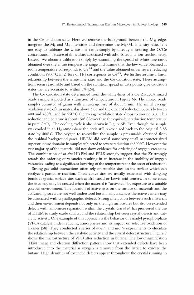
Electron energy-loss spectroscopy provides a convenient method to follow the aver-age oxidation state of the Ce when exposed to different reducing conditions. Figure 6Ashows a series of Ce M45 edges recorded from high surface-area nanoparticles of CeO2
during in situ reduction in dry H2. The large peaks at the beginning of the edge arecalled white lines and correspond to electron transitions from the 3d5/2 (M5–884 eV)and the 3d3/2 (M4–902 eV)) to unoccupied states in the 4f band. It has been shownthat the relative intensity of the M5 and M4 peaks depends on the occupancy in the 4fband, which in turn depends on the oxidation state of Ce [56]. The occupancy of the4f band changes from approximately 0 to 1 as the Ce transforms from an oxidation stateof +4 to +3. Inspection of the Ce spectra in Figure 6A shows a reversal in the relative

548 II. Electron Microscopy
0
5000
10000
15000
20000
25000
30000
870 890 910 930 950
RT
500°C
600°C
700°C
2.5
2.75
3
3.25
3.5
3.75
4
300 350 400 450 500 550 600
Temperature oC
Ce Oxidation State
A
B
Figure 6. A) Background subtracted Ce M45 peaks from pure CeO2 sample showing relative change inthe white-line intensity with temperature. A small shoulder (marked by arrow) also disappeared withreduction. B) Ce oxidation state for CeZrO2 samples showing reduction and oxidation of Ce with heating(diamonds) and cooling (squares) in dry H2.
intensities of the M5 and M4 white lines as ceria is heated from room temperature to700◦C.
There are several different methods of extracting the variation of the white-lineintensity in order to determine the occupancy of the 4f band [57]. Some of thesemethods require significant spectral processing and impose restrictive conditions onthe data acquisition. However, in the Ce system, the change in the white-line inten-sity is pronounced and thus we can use a simplified procedure to quantify changes
17. Environmental Transmission Electron Microscopy in Nanotechnology 549
in the Ce oxidation state. Here we remove the background beneath the M45 edge,integrate the M5 and M4 intensities and determine the M5/M4 intensity ratio. It isnot easy to calibrate the white-line ratios simply by directly measuring the O/Ceconcentration because of difficulties associated with adsorbates and non-stochiometry.Instead, we obtain a calibration simply by examining the spread of white-line ratiosobtained over the entire temperature range and assume that the low value obtained atroom temperature corresponds to Ce+4 and the value obtained under severe reducingconditions (800◦C in 2 Torr of H2) corresponds to Ce+3. We further assume a linearrelationship between the white-line ratio and the Ce oxidation state. These assump-tions seem reasonable and based on the statistical spread in data points give oxidationstates that are accurate to within 5% [24].
The Ce oxidation state determined from the white-lines of a CexZr1−xO2 mixedoxide sample is plotted as a function of temperature in Figure 6b. The mixed oxidesamples consisted of grains with an average size of about 5 nm. The initial averageoxidation state of this material is about 3.85 and the onset of reduction occurs between400 and 450◦C and by 550◦C the average oxidation state drops to around 3.3. Thisreduction temperature is about 150◦C lower than the equivalent reduction temperaturein pure CeO2. The cooling cycle is also shown in Figure 6B. Even though the samplewas cooled in an H2 atmosphere the ceria still re-oxidized back to the original 3.85state by 400◦C. The oxygen to re-oxidize the sample is presumable obtained fromthe residual background gases. HREM did reveal some very small nanometer sizedsuperstructure domains in samples subjected to severe reduction at 800◦C. However thevast majority of the material did not show evidence for ordering of oxygen vacancies.The combination of in-situ HREM and EELS strongly suggest that the Zr stronglyretards the ordering of vacancies resulting in an increase in the mobility of oxygenvacancies leading to a significant lowering of the temperature for the onset of reduction.
Strong gas-solid interactions often rely on suitable sites on the surface which cancatalyze a particular reaction. These active sites are usually associated with danglingbonds at special surface sites such as Bronstead or Lewis acid centers. In some cases,the sites may only be created when the material is “activated” by exposure to a suitablegaseous environment. The location of active sites on the surface of materials and theactivation process are not well understood but in many instances the active centers maybe associated with crystallographic defects. Strong interaction between such materialsand their environment depends not only on the high surface area but also on extendeddefects with nanometer separation within the crystals. Gai et al. has pioneered the useof ETEM to study oxide catalyst and the relationship between crystal defects and cat-alytic activity. One example of this approach is the behavior of vanadyl pyrophosphate(VPO) catalyst under reducing atmospheres and its impact on selective oxidation ofalkanes [58]. They conducted a series of ex-situ and in-situ experiments to elucidatethe relationship between the catalytic activity and the crystal defect structure. Figure 7shows the microstructure of VPO after reduction in butane. The low-magnificationTEM image and electron diffraction pattern show that extended defects have beenintroduced into the material as oxygen is removed from the lattice to oxidize thebutane. High densities of extended defects appear throughout the crystal running in

550 II. Electron Microscopy
Figure 7. VPO after reducing in butane. Two sets of extended defects (arrowed) parallel to [201] andsymmetry-related [201] directions in (010) orientation in diffraction contrast (∼400◦C several hours). Thediffraction pattern reveals two sets of diffuse streaks along these directions. (Gai and Kourtakis, Science,1995, reproduced with permission)
either the [201] direction or the symmetry related [201] direction. Under reducingconditions many oxygen vacancies are generated at the surfaces which diffuse into thecrystal. In this case, the lattice minimizes strain by gliding along the [201] directionswith a pure shear mechanism to reduce the misfit between the reduced surface and theadjacent matrix. The anion vacancies generated where the extended defect intersectsthe crystal surface are associated with the strong Lewis acid sites responsible for thehigh catalytic activity.
5.1.2. Evolution of Nanoparticle Systems and Sintering Mechanisms
The ambient atmosphere can strongly affect the evolution of nanoparticles givingrise to behaviors that can be much more complex than those observed under UHVconditions. Even when gross chemical transformations of the particles do not takeplace, gas induced surface effects can result in dramatic changes in particle shape

17. Environmental Transmission Electron Microscopy in Nanotechnology 551
and sintering behavior [46, 59–61]. Hansen et al. [46] have shown that the shapechange of Cu nanoparticles on a ZnO support, formed by in-situ reduction of CuO,depends upon the gaseous composition of the reducing atmosphere. Model catalystswere prepared by impregnating ZnO support with copper acetate. The formationof Cu nanocrystals during reduction in an H2 atmosphere was recorded by high-resolution imaging (Figure 8). The atomic resolution images, recorded at 280◦C in4 Torr of H2, confirm the metallic nature of the Cu particles formed (Figure 8A). Theseparticles are faceted and bound by (100), (110) and (111) lattice planes (Figure 8B).On the other hand round Cu particles were formed when the catalyst sample wasexposed to slightly oxidizing environment generated by adding H2O vapor to thehydrogen gas (Figure 8C). The shape of the Cu particle was observed to change ina more reducing environment, obtained by adding CO to hydrogen gas (Figure 8E).The Wulff ’s construction for the corresponding shapes (Figure 8B, 8D and 8F) wasused to determine surface free energies. The observed dynamic restructuring of thecatalyst shows that relevant active sites are generated during catalytic processes. Suchinformation is crucial to determine the amount of H2 adsorption on various surfacesand hence reduction rates.
Sintering and ripening processes are expected to be strongly influenced by ambientatmosphere. For example, it is well known in the catalysis literature that the presence ofoxidizing agents like water can significantly alter sintering processes. Here we illustratesintering processes for catalyst regeneration where complex interactions between thenanoparticles, the support and the ambient atmosphere result in significant noble metalsintering during low-temperatures catalyst regeneration.
Pd/alumina catalysts are widely used for hydrogenation of alkynes [62]. During thehydrogenation process, the catalysts are gradually deactivated by hydrocarbon build-upand eventually need to be regenerated. The regenerated catalysts usually exhibit lessactivity and different selectivity compared with the fresh catalysts. This phenomenonis often attributed to the decrease in the active metal surface area caused by sinteringduring the regeneration process [63]. In traditional metal particle sintering processes,significant metal atom mobility on the substrate is not achieved until the temperaturereaches about half the melting point in Kelvin (the Tamman temperature). However,the temperature during catalyst regeneration is usually much lower than the Tammantemperature of Pd (∼650◦C) and Pd is not expected to sinter easily. The catalystregeneration process was observed in the ETEM in order to determine the mechanismfor sintering at these low temperatures.
Pd/α-alumina catalysts were run in an industrial reactor for the hydrogenation ofacetylene. The catalysts were kept on-stream for 124 hours and the temperature wasvaried from 110 to 145◦F to keep a constant acetylene conversion level. Electrondiffraction and electron energy-loss spectroscopy analysis revealed that in the used cat-alysts, most of the Pd particles were lifted from the alumina surface and embedded inthe amorphous hydrocarbon material. The regeneration process was performed in situby heating the system in either steam or air to remove the hydrocarbon via either subli-mation or combustion respectively. Figure 9 shows a series of images recorded from thecatalyst while heating in 500 mTorr of air at 350◦C. The hydrocarbon develops pores

552 II. Electron Microscopy
Fig
ure
8.In
situ
TE
Mim
ages
(A,C
and
E)
ofa
Cu/
ZnO
cata
lyst
inva
riou
sga
sen
viro
nmen
tsto
geth
erw
ithth
eco
rres
pond
ing
Wul
ffco
nstr
uctio
nof
the
Cu
nano
crys
tals
(B,D
,and
F).A
)T
heim
age
was
reco
rded
ata
pres
sue
of1.
5m
bar
ofH
2at
220◦
C.T
heel
ectr
onbe
amw
aspa
ralle
lto
[011
]zo
neax
isof
Cu.
(C)
Obt
aine
din
aga
sm
ixtu
reof
H2
and
H2O
,H2:H
20
=3;
1at
ato
talp
ress
ure
of1.
5m
bar
at22
0◦C
.(E
)O
btai
ned
ina
gas
mix
ture
ofH
2(9
5%)
and
CO
(5%
)at
ato
tal
pres
sure
of5
mba
rat
220◦
C.(
Han
sen
etal
.Sc
ienc
e,20
02,r
epro
duce
dw
ithpe
rmiss
ion)

17. Environmental Transmission Electron Microscopy in Nanotechnology 553
Figure 9. Time series of used Pd/Al2O3 catalyst heating in 500 mTorr air at 350◦C for A) 0 hour;B) 1 hour C) 4 hours and D) 7 hours. Pd particles are marked and HC indicates hydrocarbon.
due in part to catalytic combustion of the hydrocarbon by the Pd particles. Calculationssuggest that the local temperature rises to about 500◦C. This is still significantly belowthe Tamman temperature (∼650◦C for Pd) and we would not normally expect atomicdiffusion of Pd to give rise to sintering. ETEM reveals several reasons for Pd sinteringin this case. First, on fresh catalyst, we have shown that major structural rearrangementscan occur within the Pd particles at temperatures as low as 500◦C [64]. This agreeswith shape transformation measurements described earlier in this chapter in whichPd nanoshells were shown to undergo significant atomic rearrangement at 500◦C.Although the atoms are mobile within the clusters, we do not see any evidence forsignificant diffusion of Pd atoms away from the clusters i.e. the atoms remain bondedto the metal cluster. However, during the regeneration process, particles are passivelybrought into physical contact via oxidation of the underlying hydrocarbon support.When physical contact between particles occurs, the high atom mobility within eachPd particle causes the two-particle cluster to rapidly reconfigure into a single crystal

554 II. Electron Microscopy
Table 3. Rate of Au Particle Growth with and Without Electron Beam
Substrate Growth Rate Electron Beam Enhanced Growth RateTemperature (atoms/cm2/sec.) Growth rate (atoms/cm2/sec.) Enhancement
125◦C 8.5 × 10¹⁰ 1.2 × 10¹³ 160150◦C 5 × 10¹¹ 1.7 × 10¹³ 140200◦C 1.2 × 10¹³ 5.8 × 10¹³ 5
cluster. This mechanism is completely different from the traditional Ostwald ripeningprocess and is the primary sintering mechanism during the regeneration of the Pdbased catalysts.
5.2. Controlled Synthesis of Nanostructures
The E-TEM can also be used as a cold-wall chemical vapor deposition (CVD) cell.The chemical vapor deposition involves precursor adsorption and dissociation on asubstrate. The materials deposited after dissociation may nucleate and grow to formnanoparticles or continuous films. The ETEM can be used for direct observation ofthe deposition process, and the nucleation and growth process. The dissociation of aprecursor (vapor) can proceed by any of the following three main mechanisms:
a) Thermal dissociation.b) Catalytic dissociationc) Electron beam induced dissociation.
An advantage of performing such experiments in an electron microscope is that we canuse imaging, diffraction and spectroscopy to simultaneously characterize the resultingmaterial in situ allowing synthesis conditions to be varied and optimized.
Drucker et al. [65, 66] have used ETEM to study the CVD process of Al and Auon SiO2 and Si surfaces respectively. They reported that the electron beam enhancedthe growth rates but the effect is lower at higher temperatures (Table 3). The observeddendritic growth of Al was believed to be responsible for the frosty and non-reflectiveappearance of Al films reported by Beach et al. [67]. Surface treatment by TiCl4produced high quality conformal Al films with growth rates dependent on pressureand temperatures. The growth rates of Au films on clean Si were observed to bedependent on temperature with a higher rate at higher temperature (Table 3). Thesemodel studies have established the validity of this technique to study CVD in situ atnear atomic level using the ETEM. Similar in-situ CVD studies can also be performedusing specially modified ultra high vacuum (UHV) TEM [68]. For example, the in situobservation of the nucleation and growth mechanism of Ge islands on clean Si surfacesunder low Ge2H6 pressures were found to follow Ostwald ripening process [69].
In an ETEM equipped with a field emission gun, nanolithography can be performedto synthesize nanostructures. The characterization techniques available in the TEM canbe employed to immediately characterize the resulting structures and understand the

17. Environmental Transmission Electron Microscopy in Nanotechnology 555
Figure 10. A) Z-contrast image of two-dimensional periodic array of GaN dots. Insert shows lineprofiles through the Z-contrast images showing FWHM of 4 nm. B) Surface plot of array of dots showingthe height of dots derived from the ADF image intensity. Average dot height 5 nm.
deposition processes. Nanolithography proceeds by admitting a gaseous precursor intothe sample area of the microscope and using the fast electron beam to locally decomposethe precursor. Electron nanolithography in a modern TEM has been demonstrated forcreating nanostructures from carbonaceous contamination and tungsten metal [70–72].However, if more exotic gaseous precursors can be designed then a much wider rangeof materials synthesis can be performed including binary compounds.
Figure 10 shows a periodic array of uniform GaN dots generated using nanolithog-raphy in the ETEM [73]. The array was generated by exposing the SiOx substrate to aunique inorganic and highly reactive hydride D2GaN3, that dissociates exothermallyunder electron irradiation resulting in formation of stoichiometric GaN and volatileand robust D2 and N2 byproducts as shown by the equation
D2GaN3 → D2 + N2 + GaN.

556 II. Electron Microscopy
This compound was previously used in GaN film growth by gas source molecular beamepitaxy to form standard heterostructures and luminescent nanostructures at extremelylow temperatures, between 150◦C and 450◦C [74]. The dot array is generated byrastering a 0.5 nm electron probe over the substrate in well define steps. The dots arehighly uniform and display an average full-width half maximum of about 4 nm, a basewidth of about 9 nm and a height of about 5 nm. Such arrays are small enough tomanifest true quantum size effects and are likely to possess unique electronic and opticalproperties which may be beneficial to optoelectronic applications and informationprocessing [75–77].
The spatial extent of the dot (5–10 nm) is considerably larger than the size of theprimary electron probe (∼0.5 nm). Similar results have recently been obtained onin situ TEM deposition of carbon nanowires and dots of tungsten metal [70, 71]. Inboth cases, features with dimensions in the range 2–5 nm were reported. Most pro-cesses for nanolithography rely on ionization of the valence electrons of the precursorspecies. The cross sections for these ionization processes are much higher for low-energy electrons and consequently the secondary electrons emitted from the surface ofthe substrate are more efficient at dissociation. For this reason in electron lithography,precursor decomposition is associated with the spatial distribution of emitted secondaryelectrons. For high-energy sub-nanometer electron probes, the spatial distribution ofsecondary electrons emitted from the surface of a thin film is controlled primarilyby the secondary electron mean free path. Careful measurements for 100 keV elec-trons show that the majority of secondary electrons are emitted with energy between2–10 eV [78, 79]. The mean free paths of secondary electrons can be estimated fromuniversal curves to lie in the range 1–5 nm [80]. Our dot dimensions are certainlyconsistent with this model and provide evidence for the strong role that secondaryelectrons play in the electron beam assisted nanolithography.
5.3. Kinetics
The kinetics of gas-solid interactions at the nanometer level can be obtained by in-situ measurements of reaction rates using an ETEM. Most of the time it is possibleto obtain the reaction rates from the time resolved data (mostly from video images).Sometimes it is possible to collect both time and temperature resolved data allowingus to estimate activation energies of the reaction process. Baker et al. [81, 82] werethe first to use ETEM to make quantitative measurements of reaction kinetics. Theyused time resolved images to measure the growth rate of carbon nanofibers at differenttemperatures for different metal particles [82]. Activation energies of carbon nanofiberformation for different catalysts were obtained from Arrhenius plots (see below). Thisinformation was used to model the growth mechanisms of carbon nanofibers bycomparing the activation energies obtained with carbon dissolution energies for variousmetal catalysts.
The reaction rate k is given by the well-known Maxwell-Boltzman equation:
k = Ae−Ea /RT

17. Environmental Transmission Electron Microscopy in Nanotechnology 557
where A is a constant called the frequency factor, Ea is the activation energy, R isthe gas constant and T is the absolute temperature. In most reactions, the rate of thereaction increases with increasing temperature. The reaction rates can be obtained bymeasuring (a) the growth rates and/or (b) conversion rates. Taking logarithms andre-arranging the Maxwell-Boltzman equation gives the Arrhenius equation:
ln k = ln A − Ea /RT
This equation shows that plotting the reaction rate against inverse temperature(Arrhenius plot) gives a straight line and the activation energy can be determineddirectly from the gradient.
5.3.1. Nucleation and Growth of Cu Nanoparticles
TiN is commonly used as a barrier layer in the semiconductor industry to retard Sidiffusion into the interconnect layer (Au, Al or Cu etc.). One of the ways to incorporatea TiN or CrN layer in very small integrated circuits is by depositing a thin layer of Tior Cr on Si or SiO2 and subjecting this layer to rapid thermal annealing in NH3 toform the respective nitride. Au, Al or Cu is then deposited to form the interconnectlayer. This two-step process could be reduced to a single step by depositing a thinlayer of Cu/Ti or Cu/Cr alloy on Si or SiO2 and performing rapid thermal annealingin NH3 at suitable temperatures. As Ti or Cr will convert to respective nitrides,Cu will be depleted from the matrix to form nanoparticles giving the desired metalcontact and nitride barrier layer. In order to understand the effect of temperature andpressure on the nitridation reaction, the process was followed by heating Cu/Ti andCu/Cr thin films, of different compositions, in ≈3–4 Torr of high purity NH3 upto 650◦C using a modified Phillips 400-T E-TEM operated at 120 KV [35]. Thenitridation temperature of Ti and Cr metals was determined by time and temperatureresolved SAED patterns [35, 36]. The growth rates of Cu particles depleted during thenitridation of Cu/Ti and Cu/Cr thin films were measured using time and temperatureresolved video imaging [36]. A typical sequence used for such measurements is shown inFigure 11. The images are digital still frames extracted from a video sequence recordedduring growth of Cu particles at 630◦C in 4 Torr of NH3. It was also observed that theCu grains do not grow isotropically, rather, certain facets have a preferential growthrate.
The area of two (of several measurements) Cu grains was plotted as a function ofannealing time during heat treatment of the CuCr film at 630◦C (Figure 12). Twogrowth regimes are observed for both grains. Growth is rapid initially (solid symbols,region A), whereas at longer anneal times, growth is slower and the grain area varieslinearly with time (open symbols, region B). This behavior indicates that for longerannealing times, the growth is controlled by diffusion of Cu in the nitride matrix.The calculated average value of the slopes of those curves, K = 3.0 ± 0.4 × 10⁻¹¹
cm2/sec, is proportional to the diffusion constant of Cu through the CrN matrix. Itshould be noted that for very long annealing times (t > 10 min), the curve becomescompletely flat as the Cu grain growth process was completed. This phenomenon

558 II. Electron Microscopy
Figure 11. A time sequence of in situ still video frames showing the growth of a Cu particle during thenitridation process of the Cu1−xCrx (x = 0.40) thin film at 630◦C. The corresponding video times inseconds are also shown in the top left of each picture.
0.2
0.4
0.6
0.8
1
1.2
1.4
0 50 100 150 200 250 300 350
Gra
in A
rea
(μm
2 )
Time (sec)
K = 3.05±0.4x10⁻¹¹
cm2/sec
Cu/Cr System
T = 630°C
A
B
Figure 12. Cu grain area measured from the video sequence shown in Figure 12 as a function of theannealing time at 630◦C when a Cu/Cr thin film was heated in ≈3 Torr of high purity NH3 gas. Thegrowth rate from two different particles given is obtained from the curves.
might be attributed to the fact that after long annealing times, Cu was fully depletedfrom the CrN matrix. Although the nitridation temperature for Ti was found tobe lower (370◦C) compared to Cr (580◦C), the growth rate of Cu particles was anorder of magnitude lower in Cr/Cu (3.05 × 10⁻¹¹ cm2/sec.) thin films than in Cu/Ti(2.2 × 10−12 − 5.0 × 10⁻¹² cm2/sec.) thin films.

17. Environmental Transmission Electron Microscopy in Nanotechnology 559
5.3.2. Carbon Nanotube Growth
Carbon nanotubes (CNTs) were dramatically novel nanoscale materials when theywere first discovered in 1991 by Iijima using a carbon arc discharge process [83]. Theyhave since become one of the most sought out materials for nanotechnology due totheir remarkable magnetic, electronic and mechanical properties [84]. The structureof a CNT can be described in terms of a single graphite layer (graphene) rolled upto form a single cylinder or concentrically arranged cylinders. The former is referredto as a single wall nanotube (SWNT) and the latter are called multiwall nanotubes(MWNTs). Although, a number of growth mechanisms have been proposed, deducedfrom high-resolution electron microscopy (HREM) images and theoretical simulations[81, 85–88], there is no direct evidence to support these models.
We have been successful in recording images of the growth of CNTs at video rate.We have used the specimen area of this microscope as a chemical vapor depositionchamber [89–90]. Our preliminary observations were made using Ni/SiO2 catalyst,and propylene and acetylene as carbon sources (precursor). Although fibrous structureswere observed to grow when propylene was used as a precursor, CNTs were observedto form only when acetylene (C2H2) was used as the precursor. Multi-wall carbonnanotubes were often observed to form with a catalyst particle at their apex, as hasbeen observed previously in HREM images of carbon nanotubes formed by the CVDprocesses.
Figures 13A–I show digitized individual frames of a typical growth process for multi-wall carbon nanotubes. A small finger shaped hollow structure (Figure 13A) movedout from the substrate, where another tube has been formed (Figure 13B), and createdthe tip of a multi-wall nanotube. After growing linearly for a short time, it curved andstarted to grow straight out again (Figure 13C). The process of changing directionscontinued until the apex anchored back to the substrate forming a loop (Figure 13D–F).CNT were often observed to grow in such a zigzag manner forming waves, spirals orloops. The length of the tube formed at the substrate to the end was used to measurethe growth rate. Measured growth rates at 475◦C and 20 m Torr of C2H2 pressurewere 38–40 nm/second (Figure 14). It is clear from the length vs. time plot (Figure 14)that the growth of the tube is not continuous. The total growth period was observedto be in the range of 1–2.5 seconds. Nanotubes were not observed to grow after1–2 seconds of their nucleation, on the other hand, new CNTs were observed tonucleate and grow during the first 2–5 minutes, after which significant deposition ofCNTs was not observed. We observed no difference in the reaction morphology orlength of CNTs formed in the area under in-situ observation or the area not irradiatedby electron beam during conditions. The growth mechanisms for various CNT arecurrently being investigated.
5.3.3. Activation Energy of Nucleation and Growth of Au Nanoparticles
Drucker et al. [65–66] had made the first in-situ observations of growth and nucle-ation mechanism of gold CVD on Si/SiOx from ethyl (trimethylphosphine) gold(Et Au(PMe3)) at different temperatures and constant pressure with time using a

560 II. Electron Microscopy
Figure 13. Individual frames digitized from a video sequence showing the nucleation and growth of amultiwall carbon nanotube. The apex is marked by arrows (A–F) showing the zigzag growth directionbending 360◦ (E) and finally attaching back to the substrate forming a loop (F). The bar is 10 nm and thetime interval between various frames is given in the top right hand corner.
modified Philips 400T ETEM [11]. Si <111> samples were cleaned by dipping inHF and quickly transferring to the microscope in order to minimize the oxidationof the Si. The samples were heated to the deposition temperature and time-resolvedimages were recorded using a video recorder. Figure 15A shows that the number ofnuclei formed did not increase with time but the Au nanoparticles grew in size. Theseparticles coalesced to form continuous thin films once their growth brought them intodirect contact with other particles [66]. The survey of the sample region not exposedto the electron beam indicated that the Au growth rates were lower in the areas notunder direct observation (Table 3). In order to obtain growth rates without electron

17. Environmental Transmission Electron Microscopy in Nanotechnology 561
CNT Growth
0
10
20
30
40
50
60
5 15 25 35 45Frame # (1/30 sec)
CN
T le
ng
th (
nm
)
Figure 14. The discontinuous growth rates for CNT measured from individual frames (1/30 second) ofthe video sequence shown in Figure 14.
beam effects, the following procedure was adopted. The precursor was introducedin the sample region for 5 minutes at deposition temperature and then the ETEMcolumn was evacuated before making TEM observations. The absence of Au particlegrowth during the observation confirmed that no residual precursor was present in thesample area and the deposition was not enhanced by the electron beam. The processwas repeated to obtain time resolved growth rates for each temperature.
The change in particle size with time at constant temperature and pressure was usedto obtain average growth rates for the Au particles. As TEM data only provides uswith two-dimensional growth rates, the height of the Au particles was measured afterdepositions using scanning tunneling microscopy. The measure change in volumethus obtained was used to determine growth rates at three different temperatures(125◦C, 150◦C and 200◦C) for depositions with and without electron beam effects(Table 3).
The logarithm of the growth rates (no of Au atoms/cm2) plotted against 1/T canthus be used to obtain the activation energy (Ea) for nucleation and growth of Aunanoparticles by CVD (Figure 15B). The slope of the curve can directly be used toobtain the activation energy using Arrhenius equation (1):
Ea = −(slope∗R)= 22.67 k cal/mole
As Au particles, once formed, were not observed to grow with time in the absenceof precursor, it is safe to assume that ripening is not responsible for the growth atthese low temperatures and the particles coalesced only when they were in directcontact. Moreover, the reported activation energy for Au surface diffusion on carbon is39 kcal/mole [91] which is higher than measured here. Therefore the activation energymeasured is for the nucleation and growth of Au during CVD.
Measurement of reaction kinetics thus provides us with an insight in to the reactionmechanisms and processes involved.

562 II. Electron Microscopy
Arrhenius Plot of Au Deposition
y = -12455x + 56.431
24
25
26
27
28
29
30
31
0.0021 0.0021 0.0022 0.0022 0.0023 0.0023 0.0024 0.0024 0.0025 0.0025 0.0026
1/T (K)
Ln
gro
wth
rat
e (a
t/cm
2 )
Figure 15. Bright field images showing nucleation and growth of Au particles on Si <111> surface at125◦C after exposure of A) 5 minutes and B) 15 minutes. C) Arrhenius plot showing the temperaturedependence of the growth rate obtained.
6. CONCLUSIONS
We have shown that ETEM is a valuable technique for understanding the responseof nanoparticle systems to a gaseous environment at near atomic-level. The modernETEM allows the dynamic behavior of the nanoparticles to be studied in real time withatomic-resolution imaging and electron diffraction in up to 50 Torr of gas pressure.On a machine equipped with a field-emission gun, electron energy-loss spectra canbe recorded using a sub-nanometer probe so that elemental and electronic structuralchanges occurring in individual nanoparticles can be followed in situ. This powerful

17. Environmental Transmission Electron Microscopy in Nanotechnology 563
combination of in-situ imaging, diffraction and spectroscopy provides detailed infor-mation about gas-solid phase transformation mechanisms in individual nanoparticles.Quantitative measurements can be used to derive reaction rates and activation ener-gies from very small areas and should allow full reaction kinetics to be determinedas a function of nanoparticles size. The ETEM can also be used to perform in-situsynthesis of nanophase materials. The simultaneous characterization can be performedduring synthesis allowing synthesis conditions to be varied and optimized rapidly.Sub-nanometer electron probes can also permit nano-lithographic structures to bedeposited and studied under a wide variety of different conditions.
REFERENCES
1. L. Marton, Bull. Acad. R. Belg. Cl. Sci., 21 (1935) 553.2. H. M. Flower, J. Microscopy, 97 (1973) 171.3. D. F. Parsons, V. R. Matricardi, R. C. Moretz and J. N. Turner, in Advances in Biological and Med-
ical Physics, Vol. 15, J. H. Lawrence and J. W. Gofman, Eds. (Academic Press, New York), (1974)p. 161.
4. D. L. Allinson, in Principles and Techniques in Elelctron Microscopy, Biological Applications, Vol. 5, M. A.Hayat, Ed. (Van Nostrand Reinhold, New York), (1975) p. 52.
5. P. Butler and K. Hale, in Practical Methods in Electron Microscopy, Vol. 9 (North Holland) (1981)pp. 239–308.
6. P. R. Swann and N. J. Tighe, Proc. 5th Eur. Reg. Cong Electron Microscopy, (1972) 436.7. G. M. Parkinson, Catalysis Letters, 2 (1989) 303.8. R. C. Doole, G. M. Parkinson, and J. M. Stead, Inst. Phys. Conf. Ser., 119 (1991) 157–160.9. R. C. Doole, G.M. Parkinson, J. L. Hutchison, M. J. Goringe and P. J. F. Harris JEOL News 30E,
(1992) 30.10. T. C. Lee, D. K. Dewald, J. A. Eades, I. M. Robertson, and H. K. Birnbaum, Rev. Sci. Instrum.
62 (1991) 1438.11. Nan Yao, Gerard E. Spinnler, Richard A. Kemp, Don C. Guthrie, R. Dwight Cates and C. Mark
Bolinger, Proc. 49th Annual; meeting of Microsc. Soc. Am. San Francisco Press (1991) 1028.12. Renu Sharma, K. Weiss, M. McKelvy and W. Glaunsinger, Proc. 52nd Ann. Meet. Microscopy Society of
America, (1994) 494–495P.13. E. D. Boyes and P. L. Gai, Ultramicroscopy, 67 (1997) 219–232.14. Pratibha L. Gai and Edward D. Boyes, in In Situ Microscopy in Materials Research, Ed. Pratibha L. Gai,
Kluwer Academic Publishers, (1997) 123–146.15. Renu Sharma and Karl Weiss, Microscopy Research and Techniques, 42 (1998) 270–280.16. L. Hansen and J. B. Wagner, Proc. 12th European Congress on Electron Microscopy, Vol. II, (2000) 537–
538.17. Thomas W. Hansen, Jacob B. Wagner, Poul L. Hansen, Seren Dahl, Haldor Topsoe, Claus J. H. Jacobson,
Science, 294 (2001) 1508–1510.18. Renu Sharma, Peter A. Crozier, Ronald Marx and Karl Weiss, Microsc. & Microanal., (2003) 912 CD.19. P. R. Swann and N. J. Tighe, Proc. 5th Eur. Reg. Cong Electron Microscopy, (1972) 360.20. M. Pan and P. A. Crozier, Ultramicroscopy, 48 (1993) 332.21. M. Pan and P. A. Crozier, Ultramicroscopy, 48 (1993) 487.22. R. F. Egerton, Electron Energy-Loss Spectroscopy in the Electron Microscope, Plenum Press, New York (1996)
Second Edition.23. P. R. Swann, in Electron Microscopy and Structure of Materials, Ed. G. Thomas, R. Fulrath and R. M.
Fisher, University of California Press (1972) 878.24. R. Sharma P. A. Crozier, Z. C. Kang, and L.Eyring, Phil. Mag. 84 (2004) 2731.25. V. Oleshko, P. A. Crozier, R. Cantrell, A. Westwood, J. of Electron Microscopy, 151 (Supplement), (2002),
S27.26. Kamino and H. Saka, Microsc. Microanal. Microstruct., 4 (1993) 127.27. R. T. K. Baker, M. A. Barber, P. S. Harris, F. S. Feates and R. J. White, J. Catalysis, 26 (1972) 51.28. R. T. K. Baker and J. J. Chludzinski, Journal of Catalysis, 64 (1980) 464.29. R. T. K. Baker, J. J. Chludzinski and C. R. F. Lund, Carbon, 25 (1987) 295–303.

564 II. Electron Microscopy
30. R. T. K. Baker, J. Of Adhesion, 52 (1995) 13–40 and references therein.31. P. L. Gai, and C. C. Torardi, Mat. Res. Soc. Symp. Proc., 404 (1996) 61.32. Pratibha. L. Gai, Kostantinos Kourtakis, and Stan Zeimecki, Microscopy and Microanalysis (2000) 6.33. Pratibha L. Gai, and Edward D. Boyes, Catal. Rev. – Sci. Eng., 34 (1992) 1–54.34. P. L. Gai, Phil. Mag., 48 (1983) 359–371.35. Z. Atzmon, R. Sharma, J. W. Mayer, and S. Q. Hong, Materials Research Society Sympos. Proceedings,
317 (1993) 245–250.36. Z. Atzmon, R. Sharma, S. W. Russell and J. W. Mayer, Materials Research Society Symp. Proceedings,
337 (1994) 619–624.37. C. A. Mims, J. J. Chludzinski, J. K. Pabst and R. T. K. Baker, J. Catalysis, 88 (1984) 97.38. R. T. K. Baker, N. S. Dudash, C. R. F. Lund and J. J. Chludzinski, Fuel, 64 (1985) 1151.39. R. T. K. Baker, J. J. Chludzinski and J. A. Dumesic, J. Catalysis, 93 (1985) 312.40. R. T. K. Baker and J. A. Dumesic, J. Phys. Chem., 90 (1986) 4730.41. E. G. Derouane, J. J. Chludzinski and R. T. K. Baker, J. Catalysis, 85 (1984) 187.42. J. A. Dumesic, S. A. Stevenson, R. D. Sherwood and R. T. K. Baker, J. Catalysis, 99 (1986) 79.43. A. J. Simoens, R. T. K. Baker, D. J. Dwyer, C. R. F. Lund and R. J. Madon, J. Catalysis, 86 (1984)
359.44. B. H. Upton, C. C. Chen, N. M. Rodriguez and R. T. K. Baker, J. Catalysis, 141 (1993) 171.45. R. T. K. Baker and N. M. Rodriguez, Energy and Fuels, 8 (1994) 330.46. P. L. Hansen, J. B. Wagner, S. Helveg, J. R. Rostrup-Nielsen, B. S. Clausen, H. Topsoe, Science 295
(2002) 2053.47. R. W. McCabe and R. K. Usmen, Studies in Surface Science and Catalysis, 101 (1996) 355.48. T. R. Baldwin and R. Burch. Applied Catalysis, 66 (1990) 359.49. A. K. Datye, D. S. Kalakkad, E. Volkl and L. F. Allard (1995). Electron Holography, 199–208.50. P. A. Crozier, R. Sharma and A. K. Datye, Microscopy and Microanalysis, 4 (1998) 278.51. P. Crozier and A. K. Datye, Studies in Surface Science and Catalysis, 130 (2000), 3119–3124.52. M. Shelef, and R. W. McCabe, Catalysis Today, 62 (2000) 35–57.53. D. J. M. Bevan and J. Kordis, J. Inorg. Chem., 26 (1964) 1509–1523.54. Z. C. Kang, J. Zhang, and L. Eyring, Z. anorg. Allg. Chem., 622 (1996) 465–472.55. P. Fornasiero, J. Kasper, and M. Graziani, J. of Catalysis, 167 (1997) 576.56. T. Manoubi, and C. Colliex, J. of Microscopy and Related Phenomena, 50 1990) 1–18.57. D. H. Pearson, C. C. Ahn, and B. Fultz, Phys. Rev., B47 (1993), 8471.58. P. L. Gai and K. Kourtakis, Science, 267 (1995) 661.59. E. G. Derouane, J. J. Chludzinski and R. T. K. Baker, J. Catalysis, 85 (1983) 187.60. K. Heinemann, T. Osaka, H. Poppa and M. Avalos-Borlja, J. Catalysis 83 (1982) 61.61. P. L. Gai, B. C. Smith and G. Owen, Nature 348 (1990) 430.62. J. Gislason W. Xia, H. Sellers J. Phys. Chem., A 106 (2002):767.63. T. B. Lin and T. C. Chou, Ind. Eng. Chem. Res., 34 (1995) 128.64. R. J. Liu et al., Microscopy and Microanalysis, in press.65. J. Drucker, R. Sharma, J. Kouvetakis and Karl Weiss, J. Appl. Phys., 77 (1995) 2846–2848.66. J. Drucker, R. Sharma, J. Kouvetakis and Karl Weiss, Proc. Mat. Res. Soc., 404 (1996) 75–84.67. D. B. Beach, S. E. Blum, and F. K. LeGoues, J. Vac. Sci. Technol., A 7 (1989) 3117.68. M. Hammar, F. K. LeGoues, J. Tersoff, M. C. Reuter and R. M. Tromp, Surface Science, 349 (1995)
129.69. F. M. Ross, J. Tersoff and R. M. Tromp, Microsc. Microanal., 4 (1998) 254.70. N. Silvis-Cividjian, C. W. Hagen, P. Kruit, M. A. J. v. d. Stam and H. B. Groen, Appl. Phys. Lett., 82
(2003) 3514.71. N. Silvis-Cividjian, C. W. Hagen, L. H. A. Leunissen, and P. Kruit, Microelectronic Engineering., 61–62
(2002) 693.72. K. Mitsuishi, M. Shimojo, M. Han, K. Furuya, Appl. Phys. Lett., 83 (2003) 2064.73. P. A. Crozier, J. Tolle, J. Kouvetakis & Cole Ritter, Appl. Phys. Lett. 84 (2004) 3441.74. L. Torrison, J. Tolle, I. S. T. Tsong, J. Kouvetakis, Thin Solid Films, 434 (2003) 106.75. Y. Arakawa, T. Someya and T. Tachibana, Phys. Stat. Sol. (b), 224 (2001) 1.76. I. D’Amico, E. Biolatti, F. Rossi, S. Derinaldis, R. Rinaldis and R. Cingolani, Superlattices and Microstruc-
tures, 31 (2002) 117.77. K. Kawasaki, D. Yamazaki, A., Kinoshita, H. Hirayama, K. Tsutsui and Y. Aoyagi, Appl. Phys. Lett., 79
(2001) 2243.78. J. Drucker, M. R. Scheinfein, J. Liu and J. K. Weiss, J. Appl. Phys., 74(12) (1993) 7329.

17. Environmental Transmission Electron Microscopy in Nanotechnology 565
79. M. R. Scheinfein, J. Drucker and J. K. Weiss, Phys. Rev., B 47(7) (1993) 4068.80. M. Prutton, Introduction to Surface Physics, Clarendon Press (1994).81. R. T. K. Baker, R. D. Sherwood and J. A. Dumesic, J. Catalysis, 66 (1980) 56.82. R. T. K. Baker, and M. A. Harris (1978), in ‘Chemistry and Physics of Carbon’, Eds. P. L. Walker, Jr.
and P. A. Thrower, Pekker, New York. Vol. 14, 83–164.83. S. Iijima, Nature, 354 (1991) 56–58.84. M. Dresselhaus, G. Dresselhaus, and Ph. Avouris (Editors), in Carbon Nanotubes: Synthesis, Structure,
Properties and Applications. Spriner-Verlag, Berln (2001) and references therein.85. Jean-Christophe Charlier, Sumio Iijima in Carbon Nanotubes: Synthesis, Structure, Properties and Applica-
tions. Spriner-Verlag, Berln (2001) 55–79.86. Y. Zhang, Y. Li, W. Kim, D. Wang, and H. Dai, Appl. Phys., A 74, 325 (2002).87. A. Maiti, C. J. Brabec, C. M. Roland, and J. Bernholc, Phys. Rev. Lett., 73 (1994) 2468–2471.88. M. Grujicic, G. Cao, and Bonnie Gersten, Materials Sci. Eng., B94 (2002) 247–259.89. Renu Sharma (2003), Microsc. & Microanal. 302CD.90. Renu Sharma and Zafar Iqbal, Appl. Phys. Lett., 84 (2004) 990.91. Mona B. Mohamed, Zhong L. Wang and Mostafa A. Al-Sayed, J. Phys. Chem. A 103 (1999) 10255.