Embed Size (px)
Citation preview

dsPIC33EPXXXGP50X,dsPIC33EPXXXMC20X/50X and
PIC24EPXXXGP/MC20X
16-Bit Microcontrollers and Digital Signal Controllers with High-Speed PWM, Op Amps and Advanced Analog
Operating Conditions• 3.0V to 3.6V, -40°C to +85°C, DC to 70 MIPS• 3.0V to 3.6V, -40°C to +125°C, DC to 60 MIPS
Core: 16-Bit dsPIC33E/PIC24E CPU• Code Efficient (C and Assembly) Architecture• Two 40-Bit-Wide Accumulators• Single Cycle (MAC/MPY) with Dual Data Fetch• Single-Cycle, Mixed-Sign MUL plus Hardware Divide• 32-Bit Multiply Support
Clock Management• 1.0% Internal Oscillator• Programmable PLLs and Oscillator Clock Sources• Fail-Safe Clock Monitor (FSCM)• Independent Watchdog Timer (WDT)• Fast Wake-up and Start-up
Power Management• Low-Power Management modes (Sleep, Idle, Doze)• Integrated Power-on Reset and Brown-out Reset• 0.6 mA/MHz Dynamic Current (typical)• 30 µA IPD Current (typical)
High-Speed PWM• Up to Three PWM Pairs with Independent Timing• Dead Time for Rising and Falling Edges • 7.14 ns PWM Resolution• PWM Support for:
- DC/DC, AC/DC, Inverters, PFC, Lighting- BLDC, PMSM, ACIM, SRM
• Programmable Fault Inputs• Flexible Trigger Configurations for ADC Conversions
Advanced Analog Features• ADC module:
- Configurable as 10-bit, 1.1 Msps with four S&H or 12-bit, 500 ksps with one S&H
- Six analog inputs on 28-pin devices and up to 16 analog inputs on 64-pin devices
• Flexible and Independent ADC Trigger Sources• Up to Three Op Amp/Comparators with
Direct Connection to the ADC module:- Additional dedicated comparator- Programmable references with 32 voltage points
• Charge Time Measurement Unit (CTMU):- Supports mTouch™ capacitive touch sensing- Provides high-resolution time measurement (1 ns)- On-chip temperature measurement
Timers/Output Compare/Input Capture• 12 General Purpose Timers:
- Five 16-bit and up to two 32-bit timers/counters- Four Output Compare (OC) modules, configurable
as timers/counters- PTG module with two configurable timers/counters- 32-bit Quadrature Encoder Interface (QEI) module,
configurable as a timer/counter• Four Input Capture (IC) modules• Peripheral Pin Select (PPS) to allow Function Remap• Peripheral Trigger Generator (PTG) for Scheduling
Complex Sequences
Communication Interfaces• Two UART modules (17.5 Mbps):
- With support for LIN/J2602 protocols and IrDA®
• Two 4-Wire SPI modules (15 Mbps)• ECAN™ module (1 Mbaud) CAN 2.0B Support• Two I2C™ modules (up to 1 Mbaud) with SMBus
Support• PPS to allow Function Remap• Programmable Cyclic Redundancy Check (CRC)
Direct Memory Access (DMA)• 4-Channel DMA with User-Selectable Priority Arbitration• UART, SPI, ADC, ECAN, IC, OC and Timers
Input/Output• Sink/Source 12 mA or 6 mA, Pin-Specific for
Standard VOH/VOL, up to 22 or 14 mA, respectively for Non-Standard VOH1
• 5V Tolerant Pins• Peripheral Pin Select (PPS) to allow Digital Function
Remapping• Selectable Open-Drain, Pull-ups and Pull-Downs• Up to 5 mA Overvoltage Clamp Current• Change Notification Interrupts on All I/O Pins
Qualification and Class B Support • AEC-Q100 REVG (Grade 1, -40°C to +125°C) Planned• AEC-Q100 REVG (Grade 0, -40°C to +150°C) Planned• Class B Safety Library, IEC 60730
Debugger Development Support• In-Circuit and In-Application Programming• Two Program and Two Complex Data Breakpoints• IEEE 1149.2 Compatible (JTAG) Boundary Scan• Trace and Run-Time Watch
2011-2013 Microchip Technology Inc. DS70000657H-page 1

dsPIC33EPXXXGP50X, dsPIC33EPXXXMC20X/50X AND PIC24EPXXXGP/MC20X
dsPIC33EPXXXGP50X, dsPIC33EPXXXMC20X/50X AND PIC24EPXXXGP/MC20X PRODUCT FAMILIES
The device names, pin counts, memory sizes andperipheral availability of each device are listed inTable 1 (General Purpose Families) and Table 2 (MotorControl Families). Their pinout diagrams appear on thefollowing pages.
TABLE 1: dsPIC33EPXXXGP50X and PIC24EPXXXGP20X GENERAL PURPOSE FAMILIES
Device
Pag
e E
ras
e S
ize
(In
str
uc
tio
ns
)
Pro
gra
m F
las
h M
emo
ry (
Kb
ytes
)
RA
M (
Kb
yte
)
Remappable Peripherals
I2 C™
CR
C G
ener
ato
r
10-B
it/1
2-B
it A
DC
(C
ha
nn
els
)
Op
Am
ps
/Co
mp
ara
tors
CT
MU
PT
G
I/O P
ins
Pin
s
Pac
kag
es
16-B
it/3
2-B
it T
ime
rs
In
pu
t C
aptu
re
Ou
tpu
t C
om
pa
re
UA
RT
SP
I(2)
EC
AN
™ T
ech
no
log
y
Ex
tern
al I
nte
rru
pts
(3)
PIC24EP32GP202 512 32 4
5 4 4 2 2 — 3 2 1 6 2/3(1) Yes Yes 21 28
SPDIP,SOIC,
SSOP(4), QFN-S
PIC24EP64GP202 1024 64 8
PIC24EP128GP202 1024 128 16
PIC24EP256GP202 1024 256 32
PIC24EP512GP202 1024 512 48
PIC24EP32GP203 512 32 45 4 4 2 2 — 3 2 1 8 3/4 Yes Yes 25 36 VTLA
PIC24EP64GP203 1024 64 8
PIC24EP32GP204 512 32 4
5 4 4 2 2 — 3 2 1 9 3/4 Yes Yes 3544/48
VTLA(4),TQFP, QFN, UQFN
PIC24EP64GP204 1024 64 8
PIC24EP128GP204 1024 128 16
PIC24EP256GP204 1024 256 32
PIC24EP512GP204 1024 512 48
PIC24EP64GP206 1024 64 8
5 4 4 2 2 — 3 2 1 16 3/4 Yes Yes 53 64TQFP,QFN
PIC24EP128GP206 1024 128 16
PIC24EP256GP206 1024 256 32
PIC24EP512GP206 1024 512 48
dsPIC33EP32GP502 512 32 4
5 4 4 2 2 1 3 2 1 6 2/3(1) Yes Yes 21 28
SPDIP,SOIC,
SSOP(4), QFN-S
dsPIC33EP64GP502 1024 64 8
dsPIC33EP128GP502 1024 128 16
dsPIC33EP256GP502 1024 256 32
dsPIC33EP512GP502 1024 512 48
dsPIC33EP32GP503 512 32 45 4 4 2 2 1 3 2 1 8 3/4 Yes Yes 25 36 VTLA
dsPIC33EP64GP503 1024 64 8
dsPIC33EP32GP504 512 32 4
5 4 4 2 2 1 3 2 1 9 3/4 Yes Yes 3544/48
VTLA(4),TQFP, QFN, UQFN
dsPIC33EP64GP504 1024 64 8
dsPIC33EP128GP504 1024 128 16
dsPIC33EP256GP504 1024 256 32
dsPIC33EP512GP504 1024 512 48
dsPIC33EP64GP506 1024 64 8
5 4 4 2 2 1 3 2 1 16 3/4 Yes Yes 53 64TQFP,QFN
dsPIC33EP128GP506 1024 128 16
dsPIC33EP256GP506 1024 256 32
dsPIC33EP512GP506 1024 512 48
Note 1: On 28-pin devices, Comparator 4 does not have external connections. Refer to Section 25.0 “Op Amp/Comparator Module” for details.2: Only SPI2 is remappable.3: INT0 is not remappable.4: The SSOP and VTLA packages are not available for devices with 512 Kbytes of memory.
DS70000657H-page 2 2011-2013 Microchip Technology Inc.

dsPIC33EPXXXGP50X, dsPIC33EPXXXMC20X/50X AND PIC24EPXXXGP/MC20X
TABLE 2: dsPIC33EPXXXMC20X/50X and PIC24EPXXXMC20X MOTOR CONTROL FAMILIES
DeviceP
ag
e E
rase
Siz
e (I
nst
ruct
ion
s)
Pro
gra
m F
lash
Mem
ory
(K
byt
es)
RA
M (
Kb
ytes
)
Remappable Peripherals
I2C
™
CR
C G
en
era
tor
10-
Bit
/12-
Bit
AD
C (
Ch
ann
els
)
Op
Am
ps/
Co
mp
arat
ors
CT
MU
PT
G
I/O
Pin
s
Pin
s
Pa
ckag
es
16-
Bit
/32-
Bit
Tim
ers
Inp
ut
Ca
ptu
re
Ou
tpu
t C
om
par
e
Mo
tor
Co
ntr
ol P
WM
(4)
(Ch
ann
els
)
Qu
ad
ratu
re E
nco
de
r In
terf
ace
UA
RT
SP
I(2)
EC
AN
™ T
ech
no
log
y
Ext
ern
al In
terr
up
ts(3
)
PIC24EP32MC202 512 32 4
5 4 4 6 1 2 2 — 3 2 1 6 2/3(1) Yes Yes 21 28
SPDIP,SOIC,
SSOP(5), QFN-S
PIC24EP64MC202 1024 64 8
PIC24EP128MC202 1024 128 16
PIC24EP256MC202 1024 256 32
PIC24EP512MC202 1024 512 48
PIC24EP32MC203 512 32 45 4 4 6 1 2 2 — 3 2 1 8 3/4 Yes Yes 25 36 VTLA
PIC24EP64MC203 1024 64 8
PIC24EP32MC204 512 32 4
5 4 4 6 1 2 2 — 3 2 1 9 3/4 Yes Yes 3544/48
VTLA(5),TQFP, QFN, UQFN
PIC24EP64MC204 1024 64 8
PIC24EP128MC204 1024 128 16
PIC24EP256MC204 1024 256 32
PIC24EP512MC204 1024 512 48
PIC24EP64MC206 1024 64 8
5 4 4 6 1 2 2 — 3 2 1 16 3/4 Yes Yes 53 64TQFP,QFN
PIC24EP128MC206 1024 128 16
PIC24EP256MC206 1024 256 32
PIC24EP512MC206 1024 512 48
dsPIC33EP32MC202 512 32 4
5 4 4 6 1 2 2 — 3 2 1 6 2/3(1) Yes Yes 21 28
SPDIP,SOIC,
SSOP(5), QFN-S
dsPIC33EP64MC202 1024 64 8
dsPIC33EP128MC202 1024 128 16
dsPIC33EP256MC202 1024 256 32
dsPIC33EP512MC202 1024 512 48
dsPIC33EP32MC203 512 32 45 4 4 6 1 2 2 — 3 2 1 8 3/4 Yes Yes 25 36 VTLA
dsPIC33EP64MC203 1024 64 8
dsPIC33EP32MC204 512 32 4
5 4 4 6 1 2 2 — 3 2 1 9 3/4 Yes Yes 3544/48
VTLA(5),TQFP, QFN, UQFN
dsPIC33EP64MC204 1024 64 8
dsPIC33EP128MC204 1024 128 16
dsPIC33EP256MC204 1024 256 32
dsPIC33EP512MC204 1024 512 48
dsPIC33EP64MC206 1024 64 8
5 4 4 6 1 2 2 — 3 2 1 16 3/4 Yes Yes 53 64TQFP,QFN
dsPIC33EP128MC206 1024 128 16
dsPIC33EP256MC206 1024 256 32
dsPIC33EP512MC206 1024 512 48
dsPIC33EP32MC502 512 32 4
5 4 4 6 1 2 2 1 3 2 1 6 2/3(1) Yes Yes 21 28
SPDIP,SOIC,
SSOP(5), QFN-S
dsPIC33EP64MC502 1024 64 8
dsPIC33EP128MC502 1024 128 16
dsPIC33EP256MC502 1024 256 32
dsPIC33EP512MC502 1024 512 48
dsPIC33EP32MC503 512 32 45 4 4 6 1 2 2 1 3 2 1 8 3/4 Yes Yes 25 36 VTLA
dsPIC33EP64MC503 1024 64 8
Note 1: On 28-pin devices, Comparator 4 does not have external connections. Refer to Section 25.0 “Op Amp/Comparator Module” for details.2: Only SPI2 is remappable.3: INT0 is not remappable.4: Only the PWM Faults are remappable.5: The SSOP and VTLA packages are not available for devices with 512 Kbytes of memory.
2011-2013 Microchip Technology Inc. DS70000657H-page 3

dsPIC33EPXXXGP50X, dsPIC33EPXXXMC20X/50X AND PIC24EPXXXGP/MC20X
dsPIC33EP32MC504 512 32 4
5 4 4 6 1 2 2 1 3 2 1 9 3/4 Yes Yes 3544/48
VTLA(5),TQFP, QFN, UQFN
dsPIC33EP64MC504 1024 64 8
dsPIC33EP128MC504 1024 128 16
dsPIC33EP256MC504 1024 256 32
dsPIC33EP512MC504 1024 512 48
dsPIC33EP64MC506 1024 64 8
5 4 4 6 1 2 2 1 3 2 1 16 3/4 Yes Yes 53 64TQFP,QFN
dsPIC33EP128MC506 1024 128 16
dsPIC33EP256MC506 1024 256 32
dsPIC33EP512MC506 1024 512 48
TABLE 2: dsPIC33EPXXXMC20X/50X and PIC24EPXXXMC20X MOTOR CONTROL FAMILIES (CONTINUED)
DeviceP
ag
e E
rase
Siz
e (I
nst
ruct
ion
s)
Pro
gra
m F
lash
Mem
ory
(K
byt
es)
RA
M (
Kb
ytes
)
Remappable Peripherals
I2C
™
CR
C G
en
era
tor
10-
Bit
/12-
Bit
AD
C (
Ch
ann
els
)
Op
Am
ps/
Co
mp
arat
ors
CT
MU
PT
G
I/O
Pin
s
Pin
s
Pa
ckag
es
16-
Bit
/32-
Bit
Tim
ers
Inp
ut
Ca
ptu
re
Ou
tpu
t C
om
par
e
Mo
tor
Co
ntr
ol P
WM
(4)
(Ch
ann
els
)
Qu
ad
ratu
re E
nco
de
r In
terf
ace
UA
RT
SP
I(2)
EC
AN
™ T
ech
no
log
y
Ext
ern
al In
terr
up
ts(3
)
Note 1: On 28-pin devices, Comparator 4 does not have external connections. Refer to Section 25.0 “Op Amp/Comparator Module” for details.2: Only SPI2 is remappable.3: INT0 is not remappable.4: Only the PWM Faults are remappable.5: The SSOP and VTLA packages are not available for devices with 512 Kbytes of memory.
DS70000657H-page 4 2011-2013 Microchip Technology Inc.

dsPIC33EPXXXGP50X, dsPIC33EPXXXMC20X/50X AND PIC24EPXXXGP/MC20X
Pin Diagrams
28-Pin SPDIP/SOIC/SSOP(1,2)
Note 1: The RPn/RPIn pins can be used by any remappable peripheral with some limitation. See Section 11.4 “Peripheral Pin Select (PPS)” for available peripherals and for information on limitations.
2: Every I/O port pin (RAx-RGx) can be used as a Change Notification pin (CNAx-CNGx). See Section 11.0 “I/O Ports” for more information.
3: There is an internal pull-up resistor connected to the TMS pin when the JTAG interface is active. See the JTAGEN bit field in Table 27-2.
= Pins are up to 5V tolerant
MCLR AVDD
AN0/OA2OUT/RA0 AVSS
AN1/C2IN1+/RA1 RPI47/T5CK/RB15
PGED3/VREF-/AN2/C2IN1-/SS1/RPI32/CTED2/RB0 RPI46/T3CK/RB14
PGEC3/VREF+/AN3/OA1OUT/RPI33/CTED1/RB1 RPI45/CTPLS/RB13
PGEC1/AN4/C1IN1+/RPI34/RB2 RPI44/RB12
PGED1/AN5/C1IN1-/RP35/RB3 TDI/RP43/RB11
TDO/RP42/RB10
OSC1/CLKI/RA2 VCAP
OSC2/CLKO/RA3 VSS
RP36/RB4 TMS/ASDA1/SDI1/RP41/RB9(3)
CVREF2O/RP20/T1CK/RA4 TCK/CVREF1O/ASCL1/SDO1/RP40/T4CK/RB8
VDD SCK1/RP39/INT0/RB7
PGED2/ASDA2/RP37/RB5 PGEC2/ASCL2/RP38/RB6
VSS
MCLR AVDD
AN0/OA2OUT/RA0 AVSS
AN1/C2IN1+/RA1 RPI47/PWM1L/T5CK/RB15
PGED3/VREF-/AN2/C2IN1-/SS1/RPI32/CTED2/RB0 RPI46/PWM1H/T3CK/RB14
PGEC3/VREF+/AN3/OA1OUT/RPI33/CTED1/RB1 RPI45/PWM2L/CTPLS/RB13
PGEC1/AN4/C1IN1+/RPI34/RB2 RPI44/PWM2H/RB12
PGED1/AN5/C1IN1-/RP35/RB3 TDI/RP43/PWM3L/RB11
TDO/RP42/PWM3H/RB10
OSC1/CLKI/RA2 VCAP
OSC2/CLKO/RA3 VSS
FLT32/RP36/RB4 TMS/ASDA1/SDI1/RP41/RB9(3)
CVREF2O/RP20/T1CK/RA4 TCK/CVREF1O/ASCL1/SDO1/RP40/T4CK/RB8
VDD SCK1/RP39/INT0/RB7
PGED2/ASDA2/RP37/RB5 PGEC2/ASCL2/RP38/RB6
VSS
1 28
2 27
3 26
4 25
5 24
6 23
7 22
8 21
9 20
10 19
11 18
12 17
13 16
14 15
PIC
24
EP
XX
XG
P2
02
ds
PIC
33
EP
XX
XG
P5
02
1 28
2 27
3 26
4 25
5 24
6 23
7 22
8 21
9 20
10 19
11 18
12 17
13 16
14 15
PIC
24
EP
XX
XM
C2
02
ds
PIC
33
EP
XX
XM
C2
02
/50
2
2011-2013 Microchip Technology Inc. DS70000657H-page 5

dsPIC33EPXXXGP50X, dsPIC33EPXXXMC20X/50X AND PIC24EPXXXGP/MC20X
Pin Diagrams (Continued)
28-Pin QFN-S(1,2,3) = Pins are up to 5V tolerant
28 27 26 25 24 23 22
8 9 10 11 12 13 14
3
18
17
16
15
4
5
7
1
2 20
19
6
21
PIC24EPXXXGP202dsPIC33EPXXXGP502
TC
K/C
VR
EF
1O
/AS
CL1
/SD
O1
/RP
40/T
4C
K/R
B8
SC
K1/
RP
39/
INT
0/R
B7
PG
EC
2/A
SC
L2/R
P38
/RB
6
PG
ED
2/A
SD
A2
/RP
37/R
B5
VD
D
CV
RE
F2O
/RP
20/T
1C
K/R
A4
RP
36/R
B4
RPI45/CTPLS/RB13
RPI44/RB12
TDI/RP43/RB11
TDO/RP42/RB10
VCAP
VSS
TMS/ASDA1/SDI1/RP41/RB9(4)R
PI4
6/T
3CK
/RB
14
RP
I47/
T5C
K/R
B15
AV
SS
AV
DD
MC
LR
AN
0/O
A2O
UT
/RA
0
AN
1/C
2IN
1+
/RA
1PGED3/VREF-/AN2/C2IN1-/SS1/RPI32/CTED2/RB0
PGEC3/VREF+/AN3/OA1OUT/RPI33/CTED1/RB1
VSS
OSC1/CLKI/RA2
OSC2/CLKO/RA3
PGEC1/AN4/C1IN1+/RPI34/RB2
PGED1/AN5/C1IN1-/RP35/RB3
Note 1: The RPn/RPIn pins can be used by any remappable peripheral with some limitation. See Section 11.4 “Peripheral Pin Select (PPS)” for available peripherals and for information on limitations.
2: Every I/O port pin (RAx-RGx) can be used as a Change Notification pin (CNAx-CNGx). See Section 11.0 “I/O Ports” for more information.
3: The metal pad at the bottom of the device is not connected to any pins and is recommended to be connected to VSS externally.
4: There is an internal pull-up resistor connected to the TMS pin when the JTAG interface is active. See the JTAGEN bit field in Table 27-2.
DS70000657H-page 6 2011-2013 Microchip Technology Inc.

dsPIC33EPXXXGP50X, dsPIC33EPXXXMC20X/50X AND PIC24EPXXXGP/MC20X
Pin Diagrams (Continued)
28-Pin QFN-S(1,2,3) = Pins are up to 5V tolerant
28 27 26 25 24 23 22
8 9 10 11 12 13 14
3
18
17
16
15
4
5
7
1
2 20
19
6
21
PIC24EPXXXMC202dsPIC33EPXXXMC202/502
TC
K/C
VR
EF
1O/A
SC
L1/
SD
O1
/RP
40/T
4C
K/R
B8
SC
K1/
RP
39/
INT
0/R
B7
PG
EC
2/A
SC
L2/R
P38
/RB
6
PG
ED
2/A
SD
A2
/RP
37/R
B5
VD
D
CV
RE
F2O
/RP
20/T
1C
K/R
A4
FLT
32/R
P36
/RB
4RPI45/PWM2L/CTPLS/RB13
RPI44/PWM2H/RB12
TDI/RP43/PWM3L/RB11
TDO/RP42/PWM3H/RB10
VCAP
VSS
TMS/ASDA1/SDI1/RP41/RB9(4)R
PI4
6/P
WM
1H/T
3C
K/R
B14
RP
I47/
PW
M1L
/T5C
K/R
B15
AV
SS
AV
DD
MC
LR
AN
0/O
A2
OU
T/R
A0
AN
1/C
2IN
1+/R
A1
PGED3/VREF-/AN2/C2IN1-/SS1/RPI32/CTED2/RB0
PGEC3/VREF+/AN3/OA1OUT/RPI33/CTED1/RB1
VSS
OSC1/CLKI/RA2
OSC2/CLKO/RA3
PGEC1/AN4/C1IN1+/RPI34/RB2
PGED1/AN5/C1IN1-/RP35/RB3
Note 1: The RPn/RPIn pins can be used by any remappable peripheral with some limitation. See Section 11.4 “Peripheral Pin Select (PPS)” for available peripherals and for information on limitations.
2: Every I/O port pin (RAx-RGx) can be used as a Change Notification pin (CNAx-CNGx). See Section 11.0 “I/O Ports” for more information.
3: The metal pad at the bottom of the device is not connected to any pins and is recommended to be connected to VSS externally.
4: There is an internal pull-up resistor connected to the TMS pin when the JTAG interface is active. See the JTAGEN bit field in Table 27-2.
2011-2013 Microchip Technology Inc. DS70000657H-page 7

dsPIC33EPXXXGP50X, dsPIC33EPXXXMC20X/50X AND PIC24EPXXXGP/MC20X
Pin Diagrams (Continued)
17
36-Pin VTLA(1,2,3)
1
10
33 32 31 30 29 28
2
3
4
5
6
24
23
22
21
20
19
11 12 13 14 15
7
8
9
343536
16 18
27
26
25
= Pins are up to 5V tolerant
PIC24EP32GP203T
CK
/CV
RE
F1O
/AS
CL
1/S
DO
1/R
P40
/T4
CK
/RB
8
RPI45/CTPLS/RB13
PGEC1/AN4/C1IN1+/RPI34/RB2
PGED1/AN5/C1IN1-/RP35/RB3
AN6/OA3OUT/C4IN1+/OCFB/RC0
AN7/C3IN1-/C4IN1-/RC1
VDD
VSS
OSC1/CLKI/RA2
OSC2/CLKO/RA3
SDA2/RPI24/RA8
RP
I46
/T3C
K/R
B14
RP
I47
/T5C
K/R
B15
AV
SS
AV
DD
MC
LR
AN
0/O
A2O
UT
/RA
0
AN
1/C
2IN
1+/R
A1
PG
ED
3/V
RE
F-/
AN
2/C
2IN
1-/
SS
1/R
PI3
2/C
TE
D2/
RB
0
PG
EC
3/V
RE
F+
/AN
3/O
A1
OU
T/R
PI3
3/C
TE
D1
/RB
1
RPI44/RB12
TDI/RP43/RB11
TDO/RP42/RB10
VCAP
VSS
RP56/RC8
TMS/ASDA1/SDI1/RP41/RB9(4)
SC
K1/
RP
39/I
NT
0/R
B7
PG
EC
2/A
SC
L2/R
P38
/RB
6
PG
ED
2/A
SD
A2
/RP
37/R
B5
VD
D
VS
S
CV
RE
F2
O/R
P20
/T1
CK
/RA
4
VD
D
SC
L2/R
P36
/RB
4
VDD
Note 1: The RPn/RPIn pins can be used by any remappable peripheral with some limitation. See Section 11.4 “Peripheral Pin Select (PPS)” for available peripherals and for information on limitations.
2: Every I/O port pin (RAx-RGx) can be used as a Change Notification pin (CNAx-CNGx). See Section 11.0 “I/O Ports” for more information.
3: The metal pad at the bottom of the device is not connected to any pins and is recommended to be connected to VSS externally.
4: There is an internal pull-up resistor connected to the TMS pin when the JTAG interface is active. See the JTAGEN bit field in Table 27-2.
dsPIC33EP32GP503
PIC24EP64GP203
dsPIC33EP64GP503
17
DS70000657H-page 8 2011-2013 Microchip Technology Inc.

dsPIC33EPXXXGP50X, dsPIC33EPXXXMC20X/50X AND PIC24EPXXXGP/MC20X
Pin Diagrams (Continued)
36-Pin VTLA(1,2,3)= Pins are up to 5V tolerant
1
10
33 32 31 30 29 28
2
3
4
5
6
24
23
22
21
20
19
11 12 13 14 15
7
8
9
343536
16 17 18
27
26
25
PIC24EP32MC203T
CK
/CV
RE
F1O
/AS
CL
1/S
DO
1/R
P40
/T4
CK
/RB
8
RPI45/PWM2L/CTPLS/RB13
PGEC1/AN4/C1IN1+/RPI34/RB2
PGED1/AN5/C1IN1-/RP35/RB3
AN6/OA3OUT/C4IN1+/OCFB/RC0
AN7/C3IN1-/C4IN1-/RC1
VDD
VSS
OSC1/CLKI/RA2
OSC2/CLKO/RA3
SDA2/RPI24/RA8
RP
I46
/PW
M1
H/T
3C
K/R
B14
RP
I47
/PW
M1
L/T
5CK
/RB
15
AV
SS
AV
DD
MC
LR
AN
0/O
A2O
UT
/RA
0
AN
1/C
2IN
1+/R
A1
PG
ED
3/V
RE
F-/
AN
2/C
2IN
1-/
SS
1/R
PI3
2/C
TE
D2/
RB
0
PG
EC
3/V
RE
F+
/AN
3/O
A1
OU
T/R
PI3
3/C
TE
D1
/RB
1
RPI44/PWM2H/RB12
TDI/RP43/PWM3L/RB11
TDO/RP42/PWM3H/RB10
VCAP
VSS
RP56/RC8
TMS/ASDA1/SDI1/RP41/RB9(4)
SC
K1/
RP
39/
INT
0/R
B7
PG
EC
2/A
SC
L2/R
P38
/RB
6
PG
ED
2/A
SD
A2
/RP
37/R
B5
VD
D
VS
S
CV
RE
F2O
/RP
20/T
1C
K/R
A4
VD
D
FLT
32/
SC
L2/R
P36
/RB
4
VDD
Note 1: The RPn/RPIn pins can be used by any remappable peripheral with some limitation. See Section 11.4 “Peripheral Pin Select (PPS)” for available peripherals and for information on limitations.
2: Every I/O port pin (RAx-RGx) can be used as a Change Notification pin (CNAx-CNGx). See Section 11.0 “I/O Ports” for more information.
3: The metal pad at the bottom of the device is not connected to any pins and is recommended to be connected to VSS externally.
4: There is an internal pull-up resistor connected to the TMS pin when the JTAG interface is active. See the JTAGEN bit field in Table 27-2.
dsPIC33EP32MC203/503
PIC24EP64MC203
dsPIC33EP64MC203/503
2011-2013 Microchip Technology Inc. DS70000657H-page 9
dsPIC33EPXXXGP50X, dsPIC33EPXXXMC20X/50X AND PIC24EPXXXGP/MC20X
Pin Diagrams (Continued)
44-Pin TQFP(1,2) = Pins are up to 5V tolerant
44
43
42
41
40
39
38
37
36
35
34
1 33
2 32
3 31
4 30
5 29
6 28
7 27
8 26
9 25
10 24
11 23
12 13 14 15 16 17 18 19 20 21 22
PIC24EPXXXGP204
TC
K/C
VR
EF
1O/A
SC
L1/R
P4
0/T
4CK
/RB
8T
DO
/RA
10
RPI45/CTPLS/RB13 PGEC1/AN4/C1IN1+/RPI34/RB2
PGED1/AN5/C1IN1-/RP35/RB3
AN6/OA3OUT/C4IN1+/OCFB/RC0
AN7/C3IN1-/C4IN1-/RC1
AN8/C3IN1+/U1RTS/BCLK1/RC2
VDD
VSS
OSC1/CLKI/RA2
OSC2/CLKO/RA3
SDA2/RPI24/RA8
SCL2/RP36/RB4
TD
I/R
A7
RP
I46
/T3C
K/R
B14
RP
I47
/T5C
K/R
B15
AV
SS
AV
DD
MC
LR
AN
0/O
A2O
UT
/RA
0
AN
1/C
2IN
1+/R
A1
PG
ED
3/V
RE
F-/
AN
2/C
2IN
1-/
SS
1/R
PI3
2/C
TE
D2/
RB
0
PG
EC
3/V
RE
F+
/AN
3/O
A1O
UT
/RP
I33/
CT
ED
1/R
B1
RPI44/RB12
RP43/RB11
RP42/RB10
VCAP
VSS
RP57/RC9
RP56/RC8
RP55/RC7
RP54/RC6
TMS/ASDA1/RP41/RB9(3)
RP
39/
INT
0/R
B7
PG
EC
2/A
SC
L2/R
P38
/RB
6
PG
ED
2/A
SD
A2/
RP
37/R
B5
VD
D
VS
S
SC
L1/
RP
I53/
RC
5
SD
A1/
RP
I52
/RC
4
SC
K1/
RP
I51
/RC
3
SD
I1/R
PI2
5/R
A9
CV
RE
F2
O/S
DO
1/R
P20
/T1
CK
/RA
4
Note 1: The RPn/RPIn pins can be used by any remappable peripheral with some limitation. See Section 11.4 “Peripheral Pin Select (PPS)” for available peripherals and for information on limitations.
2: Every I/O port pin (RAx-RGx) can be used as a Change Notification pin (CNAx-CNGx). See Section 11.0 “I/O Ports” for more information.
3: There is an internal pull-up resistor connected to the TMS pin when the JTAG interface is active. See the JTAGEN bit field in Table 27-2.
dsPIC33EPXXXGP504
DS70000657H-page 10 2011-2013 Microchip Technology Inc.

dsPIC33EPXXXGP50X, dsPIC33EPXXXMC20X/50X AND PIC24EPXXXGP/MC20X
Pin Diagrams (Continued)
44-Pin TQFP(1,2) = Pins are up to 5V tolerant
44
43
42
41
40
39
38
37
36
35
34
1 33
2 32
3 31
4 30
5 29
6 28
7 27
8 26
9 25
10 24
11 23
12
13
14
15
16
17
18
19
20
21
22
PIC24EPXXXMC204
TC
K/C
VR
EF
1O
/AS
CL1
/RP
40/T
4C
K/R
B8
TD
O/R
A1
0
RPI45/PWM2L/CTPLS/RB13 PGEC1/AN4/C1IN1+/RPI34/RB2
PGED1/AN5/C1IN1-/RP35/RB3
AN6/OA3OUT/C4IN1+/OCFB/RC0
AN7/C3IN1-/C4IN1-/RC1
AN8/C3IN1+/U1RTS/BCLK1/FLT3/RC2
VDD
VSS
OSC1/CLKI/RA2
OSC2/CLKO/RA3
SDA2/RPI24/RA8
FLT32/SCL2/RP36/RB4
TD
I/R
A7
RP
I46/
PW
M1H
/T3C
K/R
B1
4
RP
I47
/PW
M1
L/T
5CK
/RB
15
AV
SS
AV
DD
MC
LR
AN
0/O
A2
OU
T/R
A0
AN
1/C
2IN
1+/R
A1
PG
ED
3/V
RE
F-/
AN
2/C
2IN
1-/
SS
1/R
PI3
2/C
TE
D2/
RB
0
PG
EC
3/V
RE
F+
/AN
3/O
A1O
UT
/RP
I33/
CT
ED
1/R
B1
RPI44/PWM2H/RB12
RP43/PWM3L/RB11
RP42/PWM3H/RB10
VCAP
VSS
RP57/RC9
RP56/RC8
RP55/RC7
RP54/RC6
TMS/ASDA1/RP41/RB9(3)
RP
39/
INT
0/R
B7
PG
EC
2/A
SC
L2/R
P38
/RB
6
PG
ED
2/A
SD
A2/
RP
37/
RB
5
VD
D
VS
S
SC
L1/
RP
I53/
RC
5
SD
A1
/RP
I52
/RC
4
SC
K1
/RP
I51
/RC
3
SD
I1/R
PI2
5/R
A9
CV
RE
F2
O/S
DO
1/R
P20
/T1C
K/R
A4
Note 1: The RPn/RPIn pins can be used by any remappable peripheral with some limitation. See Section 11.4 “Peripheral Pin Select (PPS)” for available peripherals and for information on limitations.
2: Every I/O port pin (RAx-RGx) can be used as a Change Notification pin (CNAx-CNGx). See Section 11.0 “I/O Ports” for more information.
3: There is an internal pull-up resistor connected to the TMS pin when the JTAG interface is active. See the JTAGEN bit field in Table 27-2.
dsPIC33EPXXXMC204/504
2011-2013 Microchip Technology Inc. DS70000657H-page 11

dsPIC33EPXXXGP50X, dsPIC33EPXXXMC20X/50X AND PIC24EPXXXGP/MC20X
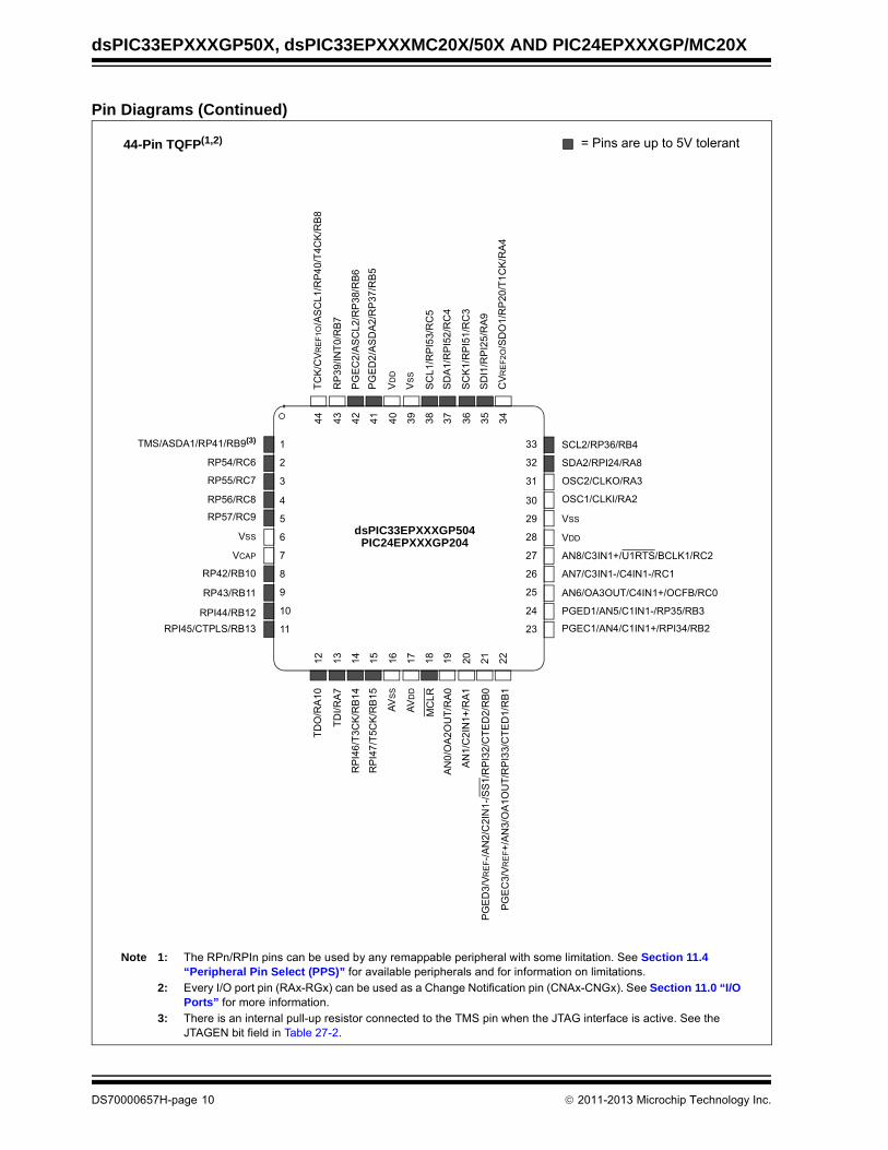
Pin Diagrams (Continued)
44-Pin VTLA(1,2,3) = Pins are up to 5V tolerant
PIC24EPXXXGP204
1
12
41 40 39 38 37 36 35 34
2
3
4
5
6
7
8
30
29
28
27
26
25
24
23
13 14 15 16 17 18 19
9
10
11 2220 21
33
32
31
424344
PGEC1/AN4/C1IN1+/RPI34/RB2
PGED1/AN5/C1IN1-/RP35/RB3
AN6/OA3OUT/C4IN1+/OCFB/RC0
AN7/C3IN1-/C4IN1-/RC1
AN8/C3IN1+/U1RTS/BCLK1/RC2
VDD
VSS
OSC1/CLKI/RA2
OSC2/CLKO/RA3
SDA2/RPI24/RA8
SCL2/RP36/RB4
TC
K/C
VR
EF
1O
/AS
CL1
/RP
40/T
4C
K/R
B8
RP
39/I
NT
0/R
B7
PG
EC
2/A
SC
L2/
RP
38/R
B6
PG
ED
2/A
SD
A2/
RP
37/R
B5
VD
D
VS
S
SC
L1/R
PI5
3/R
C5
SD
A1/
RP
I52/
RC
4
SC
K1/
RP
I51/
RC
3
SD
I1/R
PI2
5/R
A9
CV
RE
F2O
/SD
O1/
RP
20/
T1C
K/R
A4
RPI45/CTPLS/RB13
RPI44/RB12
RP43/RB11
RP42/RB10
VCAP
VSS
RP57/RC9
RP56/RC8
RP55/RC7
RP54/RC6
TMS/ASDA1/RP41/RB9(4)
TD
O/R
A10
TD
I/RA
7
RP
I46
/T3
CK
/RB
14
RP
I47
/T5
CK
/RB
15
AV
SS
AV
DD
MC
LR
AN
0/O
A2O
UT
/RA
0
AN
1/C
2IN
1+/R
A1
PG
ED
3/V
RE
F-/
AN
2/C
2IN
1-/S
S1
/RP
I32/
CT
ED
2/R
B0
PG
EC
3/V
RE
F+
/AN
3/O
A1O
UT
/RP
I33/
CT
ED
1/R
B1
Note 1: The RPn/RPIn pins can be used by any remappable peripheral with some limitation. See Section 11.4 “Peripheral Pin Select (PPS)” for available peripherals and for information on limitations.
2: Every I/O port pin (RAx-RGx) can be used as a Change Notification pin (CNAx-CNGx). See Section 11.0 “I/O Ports” for more information.
3: The metal pad at the bottom of the device is not connected to any pins and is recommended to be connected to VSS externally.
4: There is an internal pull-up resistor connected to the TMS pin when the JTAG interface is active. See the JTAGEN bit field in Table 27-2.
dsPIC33EPXXXGP504
DS70000657H-page 12 2011-2013 Microchip Technology Inc.
dsPIC33EPXXXGP50X, dsPIC33EPXXXMC20X/50X AND PIC24EPXXXGP/MC20X
Pin Diagrams (Continued)
43
44-Pin VTLA(1,2,3) = Pins are up to 5V tolerant
PIC24EPXXXMC204
1
12
41 40 39 38 37 36 35 34
2
3
4
5
6
7
8
30
29
28
27
26
25
24
23
13 14 15 16 17 18 19
9
10
11 2220 21
33
32
31
4244
PGEC1/AN4/C1IN1+/RPI34/RB2
PGED1/AN5/C1IN1-/RP35/RB3
AN6/OA3OUT/C4IN1+/OCFB/RC0
AN7/C3IN1-/C4IN1-/RC1
AN8/C3IN1+/U1RTS/BCLK1/FLT3/RC2
VDD
VSS
OSC1/CLKI/RA2
OSC2/CLKO/RA3
SDA2/RPI24/RA8
FLT32/SCL2/RP36/RB4
TC
K/C
VR
EF
1O
/AS
CL1
/RP
40/T
4C
K/R
B8
RP
39/I
NT
0/R
B7
PG
EC
2/A
SC
L2/R
P38
/RB
6
PG
ED
2/A
SD
A2/
RP
37/
RB
5
VD
D
VS
S
SC
L1/R
PI5
3/R
C5
SD
A1
/RP
I52
/RC
4
SC
K1
/RP
I51
/RC
3
SD
I1/R
PI2
5/R
A9
CV
RE
F2O
/SD
O1/
RP
20/
T1C
K/R
A4
RPI45/PWM2L/CTPLS/RB13
RPI44/PWM2H/RB12
RP43/PWM3L/RB11
RP42/PWM3H/RB10
VCAP
VSS
RP57/RC9
RP56/RC8
RP55/RC7
RP54/RC6
TMS/ASDA1/RP41/RB9(4)
TD
O/R
A10
TD
I/RA
7
RP
I46/
PW
M1H
/T3
CK
/RB
14
RP
I47/
PW
M1L
/T5
CK
/RB
15
AV
SS
AV
DD
MC
LR
AN
0/O
A2
OU
T/R
A0
AN
1/C
2IN
1+
/RA
1
PG
ED
3/V
RE
F-/
AN
2/C
2IN
1-/S
S1
/RP
I32
/CT
ED
2/R
B0
PG
EC
3/V
RE
F+
/AN
3/O
A1
OU
T/R
PI3
3/C
TE
D1
/RB
1
Note 1: The RPn/RPIn pins can be used by any remappable peripheral with some limitation. See Section 11.4 “Peripheral Pin Select (PPS)” for available peripherals and for information on limitations.
2: Every I/O port pin (RAx-RGx) can be used as a Change Notification pin (CNAx-CNGx). See Section 11.0 “I/O Ports” for more information.
3: The metal pad at the bottom of the device is not connected to any pins and is recommended to be connected to VSS externally.
4: There is an internal pull-up resistor connected to the TMS pin when the JTAG interface is active. See the JTAGEN bit field in Table 27-2.
dsPIC33EPXXXMC204/504
2011-2013 Microchip Technology Inc. DS70000657H-page 13

dsPIC33EPXXXGP50X, dsPIC33EPXXXMC20X/50X AND PIC24EPXXXGP/MC20X
Pin Diagrams (Continued)
44-Pin QFN(1,2,3) = Pins are up to 5V tolerant
44 43 42 41 40 39 38 37 36 35
12 13 14 15 16 17 18 19 20 21
3
30
29
28
27
26
25
24
23
4
5
7
8
9
10
11
1
2 32
31
6
22
33
34
PIC24EPXXXGP204
PGEC1/AN4/C1IN1+/RPI34/RB2
PGED1/AN5/C1IN1-/RP35/RB3
AN6/OA3OUT/C4IN1+/OCFB/RC0
AN7/C3IN1-/C4IN1-/RC1
AN8/C3IN1+/U1RTS/BCLK1/RC2
VDD
VSS
OSC1/CLKI/RA2
OSC2/CLKO/RA3
SDA2/RPI24/RA8
SCL2/RP36/RB4
TC
K/C
VR
EF
1O/A
SC
L1/
RP
40/T
4CK
/RB
8
RP
39/IN
T0/
RB
7
PG
EC
2/A
SC
L2/
RP
38/
RB
6
PG
ED
2/A
SD
A2
/RP
37/R
B5
VD
D
VS
S
SC
L1/R
PI5
3/R
C5
SD
A1/
RP
I52/
RC
4
SC
K1/
RP
I51/
RC
3
SD
I1/R
PI2
5/R
A9
CV
RE
F2O
/SD
O1/
RP
20/T
1CK
/RA
4
RPI45/CTPLS/RB13
RPI44/RB12
RP43/RB11
RP42/RB10
VCAP
VSS
RP57/RC9
RP56/RC8
RP55/RC7
RP54/RC6
TMS/ASDA1/RP41/RB9(4)
TD
O/R
A10
TD
I/RA
7
RP
I46
/T3
CK
/RB
14
RP
I47
/T5
CK
/RB
15
AV
SS
AV
DD
MC
LR
AN
0/O
A2O
UT
/RA
0
AN
1/C
2IN
1+/R
A1
PG
ED
3/V
RE
F-/
AN
2/C
2IN
1-/S
S1
/RP
I32
/CT
ED
2/R
B0
PG
EC
3/V
RE
F+
/AN
3/O
A1
OU
T/R
PI3
3/C
TE
D1/
RB
1
dsPIC33EPXXXGP504
Note 1: The RPn/RPIn pins can be used by any remappable peripheral with some limitation. See Section 11.4 “Peripheral Pin Select (PPS)” for available peripherals and for information on limitations.
2: Every I/O port pin (RAx-RGx) can be used as a Change Notification pin (CNAx-CNGx). See Section 11.0 “I/O Ports” for more information.
3: The metal pad at the bottom of the device is not connected to any pins and is recommended to be connected to VSS externally.
4: There is an internal pull-up resistor connected to the TMS pin when the JTAG interface is active. See the JTAGEN bit field in Table 27-2.
DS70000657H-page 14 2011-2013 Microchip Technology Inc.

dsPIC33EPXXXGP50X, dsPIC33EPXXXMC20X/50X AND PIC24EPXXXGP/MC20X
Pin Diagrams (Continued)
44-Pin QFN(1,2,3) = Pins are up to 5V tolerant
44 43 42 41 40 39 38 37 36 35
12 13 14 15 16 17 18 19 20 21
3
30
29
28
27
26
25
24
23
4
5
7
8
9
10
11
1
2 32
31
6
22
33
34
PIC24EPXXXMC204
PGEC1/AN4/C1IN1+/RPI34/RB2
PGED1/AN5/C1IN1-/RP35/RB3
AN6/OA3OUT/C4IN1+/OCFB/RC0
AN7/C3IN1-/C4IN1-/RC1
AN8/C3IN1+/U1RTS/BCLK1/FLT3/RC2
VDD
VSS
OSC1/CLKI/RA2
OSC2/CLKO/RA3
SDA2/RPI24/RA8
FLT32/SCL2/RP36/RB4
TC
K/C
VR
EF
1O/A
SC
L1/
RP
40/
T4C
K/R
B8
RP
39/IN
T0/
RB
7
PG
EC
2/A
SC
L2/R
P3
8/R
B6
PG
ED
2/A
SD
A2
/RP
37/R
B5
VD
D
VS
S
SC
L1/R
PI5
3/R
C5
SD
A1/
RP
I52/
RC
4
SC
K1/
RP
I51/
RC
3
SD
I1/R
PI2
5/R
A9
CV
RE
F2
O/S
DO
1/R
P20
/T1
CK
/RA
4
RPI45/PWM2L/CTPLS/RB13
RPI44/PWM2H/RB12
RP43/PWM3L/RB11
RP42/PWM3H/RB10
VCAP
VSS
RP57/RC9
RP56/RC8
RP55/RC7
RP54/RC6
TMS/ASDA1/RP41/RB9(4)
TD
O/R
A10
TD
I/RA
7
RP
I46
/PW
M1
H/T
3C
K/R
B14
RP
I47/
PW
M1L
/T5
CK
/RB
15
AV
SS
AV
DD
MC
LR
AN
0/O
A2O
UT
/RA
0
AN
1/C
2IN
1+/R
A1
PG
ED
3/V
RE
F-/
AN
2/C
2IN
1-/S
S1/
RP
I32/
CT
ED
2/R
B0
PG
EC
3/V
RE
F+
/AN
3/O
A1O
UT
/RP
I33/
CT
ED
1/R
B1
dsPIC33EPXXXMC204/504
Note 1: The RPn/RPIn pins can be used by any remappable peripheral with some limitation. See Section 11.4 “Peripheral Pin Select (PPS)” for available peripherals and for information on limitations.
2: Every I/O port pin (RAx-RGx) can be used as a Change Notification pin (CNAx-CNGx). See Section 11.0 “I/O Ports” for more information.
3: The metal pad at the bottom of the device is not connected to any pins and is recommended to be connected to VSS externally.
4: There is an internal pull-up resistor connected to the TMS pin when the JTAG interface is active. See the JTAGEN bit field in Table 27-2.
2011-2013 Microchip Technology Inc. DS70000657H-page 15

dsPIC33EPXXXGP50X, dsPIC33EPXXXMC20X/50X AND PIC24EPXXXGP/MC20X
Pin Diagrams (Continued)
48-Pin UQFN(1,2,3) = Pins are up to 5V tolerant
Note 1: The RPn/RPIn pins can be used by any remappable peripheral with some limitation. See Section 11.4 “Peripheral Pin Select (PPS)” for available peripherals and for information on limitations.
2: Every I/O port pin (RAx-RGx) can be used as a Change Notification pin (CNAx-CNGx). See Section 11.0 “I/O Ports” for more information.
3: The metal pad at the bottom of the device is not connected to any pins and is recommended to be connected to VSS externally.
4: There is an internal pull-up resistor connected to the TMS pin when the JTAG interface is active. See the JTAGEN bit field in Table 27-2.
48 47 46 45 43 42 41 40 39 38
13 14 15 16 17 18 19 21 22 23
3
33
31
30
29
28
27
26
25
4
5
7
9
10
11
12
1
2 35
34
6
24
36
37
PIC24EPXXXGP204
PGEC1/AN4/C1IN1+/RPI34/RB2
PGED1/AN5/C1IN1-/RP35/RB3
AN6/OA3OUT/C4IN1+/OCFB/RC0
AN7/C3IN1-/C4IN1-/RC1
AN8/C3IN1+/U1RTS/BCLK1/RC2
VDD
VSS
OSC1/CLKI/RA2
OSC2/CLKO/RA3
SDA2/RPI24/RA8
SCL2/RP36/RB4
TC
K/C
VR
EF
1O
/AS
CL1
/RP
40/T
4C
K/R
B8
RP
39/I
NT
0/R
B7
PG
EC
2/A
SC
L2/
RP
38/R
B6
PG
ED
2/A
SD
A2/
RP
37/
RB
5
VD
D
VS
S
SC
L1/R
PI5
3/R
C5
SD
A1/
RP
I52/
RC
4
SC
K1/
RP
I51/
RC
3
SD
I1/R
PI2
5/R
A9
CV
RE
F2O
/SD
O1/
RP
20/
T1C
K/R
A4
RPI45/CTPLS/RB13
RPI44/RB12
RP43/RB11
RP42/RB10
VCAP
VSS
RP57/RC9
RP56/RC8
RP55/RC7
RP54/RC6
TMS/ASDA1/RP41/RB9(4)
TD
O/R
A1
0
TD
I/R
A7
RP
I46/
T3C
K/R
B1
4
RP
I47/
T5C
K/R
B1
5
AV
SS
AV
DD
MC
LR
AN
0/O
A2
OU
T/R
A0
AN
1/C
2IN
1+
/RA
1
PG
ED
3/V
RE
F-/
AN
2/C
2IN
1-/S
S1
/RP
I32
/CT
ED
2/R
B0
PG
EC
3/V
RE
F+
/AN
3/O
A1
OU
T/R
PI3
3/C
TE
D1
/RB
1dsPIC33EPXXXGP504
8N/C
20
N/C
32 N/C
44N
/C
DS70000657H-page 16 2011-2013 Microchip Technology Inc.

dsPIC33EPXXXGP50X, dsPIC33EPXXXMC20X/50X AND PIC24EPXXXGP/MC20X
Pin Diagrams (Continued)
48-Pin UQFN(1,2,3) = Pins are up to 5V tolerant
Note 1: The RPn/RPIn pins can be used by any remappable peripheral with some limitation. See Section 11.4 “Peripheral Pin Select (PPS)” for available peripherals and for information on limitations.
2: Every I/O port pin (RAx-RGx) can be used as a Change Notification pin (CNAx-CNGx). See Section 11.0 “I/O Ports” for more information.
3: The metal pad at the bottom of the device is not connected to any pins and is recommended to be connected to VSS externally.
4: There is an internal pull-up resistor connected to the TMS pin when the JTAG interface is active. See the JTAGEN bit field in Table 27-2.
48 47 46 45 43 42 41 40 39 38
13 14 15 16 17 18 19 21 22 23
3
33
31
30
29
28
27
26
25
4
5
7
9
10
11
12
1
2 35
34
6
24
36
37
PIC24EPXXXMC204
PGEC1/AN4/C1IN1+/RPI34/RB2
PGED1/AN5/C1IN1-/RP35/RB3
AN6/OA3OUT/C4IN1+/OCFB/RC0
AN7/C3IN1-/C4IN1-/RC1
AN8/C3IN1+/U1RTS/BCLK1/FLT3/RC2
VDD
VSS
OSC1/CLKI/RA2
OSC2/CLKO/RA3
SDA2/RPI24/RA8
FLT32/SCL2/RP36/RB4
TC
K/C
VR
EF
1O
/AS
CL1
/RP
40/T
4C
K/R
B8
RP
39/I
NT
0/R
B7
PG
EC
2/A
SC
L2/R
P38
/RB
6
PG
ED
2/A
SD
A2/
RP
37/
RB
5
VD
D
VS
S
SC
L1/R
PI5
3/R
C5
SD
A1
/RP
I52/
RC
4
SC
K1
/RP
I51/
RC
3
SD
I1/R
PI2
5/R
A9
CV
RE
F2O
/SD
O1/
RP
20/
T1C
K/R
A4
RPI45/PWM2L/CTPLS/RB13
RPI44/PWM2H/RB12
RP43/PWM3L/RB11
RP42/PWM3H/RB10
VCAP
VSS
RP57/RC9
RP56/RC8
RP55/RC7
RP54/RC6
TMS/ASDA1/RP41/RB9(4)
TD
O/R
A1
0
TD
I/R
A7
RP
I46/
PW
M1H
/T3C
K/R
B1
4
RP
I47/
PW
M1
L/T
5CK
/RB
15
AV
SS
AV
DD
MC
LR
AN
0/O
A2
OU
T/R
A0
AN
1/C
2IN
1+
/RA
1
PG
ED
3/V
RE
F-/
AN
2/C
2IN
1-/
SS
1/R
PI3
2/C
TE
D2
/RB
0
PG
EC
3/V
RE
F+
/AN
3/O
A1
OU
T/R
PI3
3/C
TE
D1
/RB
1
dsPIC33EPXXXMC204/504
8N/C
20
N/C
32 N/C
44N
/C
2011-2013 Microchip Technology Inc. DS70000657H-page 17

dsPIC33EPXXXGP50X, dsPIC33EPXXXMC20X/50X AND PIC24EPXXXGP/MC20X
Pin Diagrams (Continued)
64 63 62 61 60 59 58 57 56 55 54 53 52 51 50 49
1 48
2 47
3 46
4 455 44
6 43
7 42
8 419 40
10 39
11 38
12 37
13 36
14 35
15 34
16 33
17 18 19 20 21 22 23 24 25 26 27 28 29 30 31 32
TDI/RA7
RPI46/T3CK/RB14
RPI47/T5CK/RB15
RP118/RG6
RPI119/RG7
RP120/RG8
MCLR
RPI121/RG9
VSS
VDD
AN10/RPI28/RA12
AN9/RPI27/RA11
AN0/OA2OUT/RA0
AN1/C2IN1+/RA1
PGED3/VREF-/AN2/C2IN1-/SS1/RPI32/CTED2/RB0
PGEC3/VREF+/AN3/OA1OUT/RPI33/CTED1/RB1
TD
O/R
A10
RP
I45/
CT
PLS
/RB
13
RP
I44/
RB
12
RP
43/R
B11
RP
42/R
B10
RP
97/R
F1
RP
I96/
RF
0
VD
D
VC
AP
RP
57/R
C9
RD
6
RD
5
RP
56/R
C8
RP
55/R
C7
RP
54/R
C6
TM
S/A
SD
A1/
RP
41/R
B9(4
)
TCK/CVREF1O/ASCL1/RP40/T4CK/RB8
RC13
RP39/INT0/RB7
RPI58/RC10
PGEC2/ASCL2/RP38/RB6
PGED2/ASDA2/RP37/RB5
RD8
VSS
OSC2/CLKO/RC15
OSC1/CLKI/RC12
VDD
SCL1/RPI53/RC5
SDA1/RPI52/RC4
SCK1/RPI51/RC3
SDI1/RPI25/RA9
CVREF2O/SDO1/RP20/T1CK/RA4
PG
EC
1/A
N4/
C1I
N1+
/RP
I34/
RB
2
PG
ED
1/A
N5/
C1I
N1-
/RP
35/R
B3
AV
DD
AV
SS
AN
6/O
A3O
UT
/C4I
N1+
/OC
FB
/RC
0
AN
7/C
3IN
1-/C
4IN
1-/R
C1
AN
8/C
3IN
1+/U
1RT
S/B
CLK
1/R
C2
AN
11/C
1IN
2-(3
) /U1C
TS
/RC
11
VS
S
VD
D
AN
12/C
2IN
2-(3
) /U2R
TS
/BC
LK2/
RE
12
AN
13/C
3IN
2-(3
) /U2C
TS
/RE
13
AN
14/R
PI9
4/R
E14
AN
15/R
PI9
5/R
E15
SD
A2/
RP
I24/
RA
8
SC
L2/R
P36
/RB
4
dsPIC33EP64GP506
PIC24EP64GP206PIC24EP128GP206PIC24EP256GP206
dsPIC33EP128GP506dsPIC33EP256GP506dsPIC33EP512GP506
PIC24EP512GP206
Note 1: The RPn/RPIn pins can be used by any remappable peripheral with some limitation. See Section 11.4 “Peripheral Pin Select (PPS)” for available peripherals and for information on limitations.
2: Every I/O port pin (RAx-RGx) can be used as a Change Notification pin (CNAx-CNGx). See Section 11.0 “I/O Ports” for more information.
3: The metal pad at the bottom of the device is not connected to any pins and is recommended to be connected to VSS externally.
4: There is an internal pull-up resistor connected to the TMS pin when the JTAG interface is active. See the JTAGEN bit field in Table 27-2.
64-Pin TQFP(1,2,3) = Pins are up to 5V tolerant
DS70000657H-page 18 2011-2013 Microchip Technology Inc.

dsPIC33EPXXXGP50X, dsPIC33EPXXXMC20X/50X AND PIC24EPXXXGP/MC20X
Pin Diagrams (Continued)
64-Pin TQFP(1,2,3) = Pins are up to 5V tolerant
64 63 62 61 60 59 58 57 56 55 54 53 52 51 50 49
1 48
2 47
3 46
4 45
5 44
6 43
7 42
8 41
9 40
10 39
11 38
12 37
13 36
14 35
15 34
16 33
17 18 19 20 21 22 23 24 25 26 27 28 29 30 31 32
TDI/RA7
RPI46/PWM1H/T3CK/RB14
RPI47/PWM1L/T5CK/RB15
RP118/RG6
RPI119/RG7
RP120/RG8
MCLR
RPI121/RG9
VSS
VDD
AN10/RPI28/RA12
AN9/RPI27/RA11
AN0/OA2OUT/RA0
AN1/C2IN1+/RA1
PGED3/VREF-/AN2/C2IN1-/SS1/RPI32/CTED2/RB0
PGEC3/VREF+/AN3/OA1OUT/RPI33/CTED1/RB1
TD
O/R
A1
0
RP
I45
/PW
M2
L/C
TP
LS
/RB
13
RP
I44/
PW
M2H
/RB
12
RP
43/P
WM
3L/R
B11
RP
42/P
WM
3H/R
B1
0
RP
97/R
F1
RP
I96/
RF
0
VD
D
VC
AP
RP
57/R
C9
RD
6
RD
5
RP
56/R
C8
RP
55/R
C7
RP
54/R
C6
TM
S/A
SD
A1
/RP
41
/RB
9(4
)
TCK/CVREF1O/ASCL1/RP40/T4CK/RB8
RC13
RP39/INT0/RB7
RPI58/RC10
PGEC2/ASCL2/RP38/RB6
PGED2/ASDA2/RP37/RB5
RD8
VSS
OSC2/CLKO/RC15
OSC1/CLKI/RC12
VDD
SCL1/RPI53/RC5
SDA1/RPI52/RC4
SCK1/RPI51/RC3
SDI1/RPI25/RA9
CVREF2O/SDO1/RP20/T1CK/RA4
PG
EC
1/A
N4
/C1I
N1
+/R
PI3
4/R
B2
PG
ED
1/A
N5
/C1I
N1
-/R
P3
5/R
B3
AV
DD
AV
SS
AN
6/O
A3O
UT
/C4I
N1+
/OC
FB
/RC
0
AN
7/C
3IN
1-/
C4
IN1
-/R
C1
AN
8/C
3IN
1+
/U1R
TS
/BC
LK1/
FLT
3/R
C2
AN
11/C
1IN
2-(3
) /U1C
TS
/FLT
4/R
C11
VS
S
VD
D
AN
12
/C2I
N2
-(3) /U
2RT
S/B
CL
K2
/RE
12
AN
13/
C3
IN2
-(3) /U
2CT
S/R
E13
AN
14
/RP
I94
/RE
14
AN
15
/RP
I95
/RE
15
SD
A2
/RP
I24
/RA
8
FLT
32
/SC
L2
/RP
36
/RB
4
PIC24EP64MC206
dsPIC33EP64MC206/506
PIC24EP128MC206PIC24EP256MC206
dsPIC33EP128MC206/506dsPIC33EP256MC206/506dsPIC33EP512MC206/506
PIC24EP512MC206
Note 1: The RPn/RPIn pins can be used by any remappable peripheral with some limitation. See Section 11.4 “Peripheral Pin Select (PPS)” for available peripherals and for information on limitations.
2: Every I/O port pin (RAx-RGx) can be used as a Change Notification pin (CNAx-CNGx). See Section 11.0 “I/O Ports” for more information.
3: The metal pad at the bottom of the device is not connected to any pins and is recommended to be connected to VSS externally.
4: There is an internal pull-up resistor connected to the TMS pin when the JTAG interface is active. See the JTAGEN bit field in Table 27-2.
2011-2013 Microchip Technology Inc. DS70000657H-page 19

dsPIC33EPXXXGP50X, dsPIC33EPXXXMC20X/50X AND PIC24EPXXXGP/MC20X
Pin Diagrams (Continued)
64-Pin QFN(1,2,3,4) = Pins are up to 5V tolerant
TD
O/R
A1
0
RP
I45/
CT
PLS
/RB
13
RP
I44/
RB
12
RP
43/R
B11
RP
42/R
B1
0
RP
97/R
F1
RP
I96/
RF
0
VD
D
VC
AP
RP
57/R
C9
RD
6
RD
5
RP
56/R
C8
RP
55/R
C7
RP
54/R
C6
TM
S/A
SD
A1
/RP
41
/RB
9(5)
TCK/CVREF1O/ASCL1/RP40/T4CK/RB8
RC13
RP39/INT0/RB7
RPI58/RC10
PGEC2/ASCL2/RP38/RB6
PGED2/ASDA2/RP37/RB5RD8
VSS
OSC2/CLKO/RC15
OSC1/CLKI/RC12VDD
SCL1/RPI53/RC5SDA1/RPI52/RC4
SCK1/RPI51/RC3
SDI1/RPI25/RA9
CVREF2O/SDO1/RP20/T1CK/RA4
PG
EC
1/A
N4
/C1I
N1
+/R
PI3
4/R
B2
PG
ED
1/A
N5
/C1I
N1
-/R
P3
5/R
B3
AV
DD
AV
SS
AN
6/O
A3O
UT
/C4I
N1+
/OC
FB
/RC
0
AN
7/C
3IN
1-/C
4IN
1-/R
C1
AN
8/C
3IN
1+
/U1
RT
S/B
CLK
1/R
C2
AN
11/C
1IN
2-(3
) /U1C
TS
/RC
11
VS
S
VD
D
AN
12
/C2I
N2
-(3) /U
2RT
S/B
CL
K2
/RE
12
AN
13
/C3
IN2
-(3) /U
2CT
S/R
E1
3
AN
14
/RP
I94
/RE
14
AN
15
/RP
I95
/RE
15
SD
A2
/RP
I24
/RA
8
SC
L2/
RP
36
/RB
4
TDI/RA7
RPI46/T3CK/RB14RPI47/T5CK/RB15
RP118/RG6RPI119/RG7
RP120/RG8MCLR
RPI121/RG9VSS
VDD
AN10/RPI28/RA12
AN9/RPI27/RA11
AN0/OA2OUT/RA0
AN1/C2IN1+/RA1
PGED3/VREF-/AN2/C2IN1-/SS1/RPI32/CTED2/RB0
PGEC3/VREF+/AN3/OA1OUT/RPI33/CTED1/RB1
PIC24EP64GP206
64
63
62
61
60
59
58
57
56
55
54
53
52
51
50
49
1 48
2 47
3 46
4 45
5 44
6 43
7 42
8 41
9 40
10 39
11 38
12 37
13 36
14 35
15 34
16 33
17
18
19
20
21
22
23
24
25
26
27
28
29
30
31
32
Note 1: The RPn/RPIn pins can be used by any remappable peripheral with some limitation. See Section 11.4 “Peripheral Pin Select (PPS)” for available peripherals and for information on limitations.
2: Every I/O port pin (RAx-RGx) can be used as a Change Notification pin (CNAx-CNGx). See Section 11.0 “I/O Ports” for more information.
3: This pin is not available as an input when OPMODE (CMxCON<10>) = 1.4: The metal pad at the bottom of the device is not connected to any pins and is recommended to be connected
to VSS externally.5: There is an internal pull-up resistor connected to the TMS pin when the JTAG interface is active. See the
JTAGEN bit field in Table 27-2.
dsPIC33EP64GP506
PIC24EP128GP206PIC24EP256GP206
dsPIC33EP128GP506dsPIC33EP256GP506dsPIC33EP512GP506
PIC24EP512GP206
DS70000657H-page 20 2011-2013 Microchip Technology Inc.

dsPIC33EPXXXGP50X, dsPIC33EPXXXMC20X/50X AND PIC24EPXXXGP/MC20X
Pin Diagrams (Continued)
64-Pin QFN(1,2,3,4) = Pins are up to 5V tolerant
64
63
62
61
60
59
58
57
56
55
54
53
52
51
50
49
1 48
2 47
3 46
4 45
5 44
6 43
7 42
8 41
9 40
10 39
11 38
12 37
13 36
14 35
15 34
16 33
17
18
19
20
21
22
23
24
25
26
27
28
29
30
31
32
TD
O/R
A1
0
RP
I45
/PW
M2L
/CT
PL
S/R
B1
3
RP
I44/
PW
M2H
/RB
12
RP
43/P
WM
3L/R
B11
RP
42/P
WM
3H/R
B10
RP
97/R
F1
RP
I96/
RF
0
VD
D
VC
AP
RP
57/R
C9
RD
6
RD
5
RP
56/R
C8
RP
55/R
C7
RP
54/R
C6
TM
S/A
SD
A1
/RP
41
/RB
9(5)
TCK/CVREF1O/ASCL1/RP40/T4CK/RB8
RC13
RP39/INT0/RB7
RPI58/RC10
PGEC2/ASCL2/RP38/RB6
PGED2/ASDA2/RP37/RB5RD8
VSS
OSC2/CLKO/RC15
OSC1/CLKI/RC12VDD
SCL1/RPI53/RC5SDA1/RPI52/RC4
SCK1/RPI51/RC3
SDI1/RPI25/RA9
CVREF2O/SDO1/RP20/T1CK/RA4
PG
EC
1/A
N4
/C1
IN1
+/R
PI3
4/R
B2
PG
ED
1/A
N5
/C1I
N1
-/R
P3
5/R
B3
AV
DD
AV
SS
AN
6/O
A3O
UT
/C4I
N1+
/OC
FB
/RC
0
AN
7/C
3IN
1-/
C4I
N1-
/RC
1
AN
8/C
3IN
1+
/U1
RT
S/B
CLK
1/F
LT3/
RC
2
AN
11/C
1IN
2-(3
) /U1C
TS
/FLT
4/R
C11
VS
S
VD
D
AN
12
/C2
IN2
-(3) /U
2RT
S/B
CL
K2
/RE
12
AN
13
/C3I
N2
-(3) /U
2CT
S/R
E13
AN
14
/RP
I94
/RE
14
AN
15
/RP
I95
/RE
15
SD
A2
/RP
I24
/RA
8
FLT
32
/SC
L2/
RP
36
/RB
4
TDI/RA7
RPI46/PWM1H/T3CK/RB14RPI47/PWM1L/T5CK/RB15
RP118/RG6RPI119/RG7
RP120/RG8MCLR
RPI121/RG9VSS
VDD
AN10/RPI28/RA12
AN9/RPI27/RA11
AN0/OA2OUT/RA0
AN1/C2IN1+/RA1
PGED3/VREF-/AN2/C2IN1-/SS1/RPI32/CTED2/RB0
PGEC3/VREF+/AN3/OA1OUT/RPI33/CTED1/RB1
PIC24EP64MC206
dsPIC33EP64MC206/506
PIC24EP128MC206PIC24EP256MC206
dsPIC33EP128MC206/506dsPIC33EP256MC206/506dsPIC33EP512MC206/506
PIC24EP512MC206
Note 1: The RPn/RPIn pins can be used by any remappable peripheral with some limitation. See Section 11.4 “Peripheral Pin Select (PPS)” for available peripherals and for information on limitations.
2: Every I/O port pin (RAx-RGx) can be used as a Change Notification pin (CNAx-CNGx). See Section 11.0 “I/O Ports” for more information.
3: This pin is not available as an input when OPMODE (CMxCON<10>) = 1.4: The metal pad at the bottom of the device is not connected to any pins and is recommended to be connected
to VSS externally.
5: There is an internal pull-up resistor connected to the TMS pin when the JTAG interface is active. See the JTAGEN bit field in Table 27-2.
2011-2013 Microchip Technology Inc. DS70000657H-page 21
dsPIC33EPXXXGP50X, dsPIC33EPXXXMC20X/50X AND PIC24EPXXXGP/MC20X
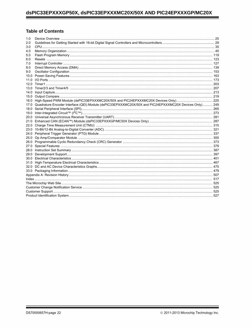
Table of Contents
1.0 Device Overview ........................................................................................................................................................................ 252.0 Guidelines for Getting Started with 16-bit Digital Signal Controllers and Microcontrollers ......................................................... 293.0 CPU............................................................................................................................................................................................ 354.0 Memory Organization ................................................................................................................................................................. 455.0 Flash Program Memory............................................................................................................................................................ 1196.0 Resets ..................................................................................................................................................................................... 1237.0 Interrupt Controller ................................................................................................................................................................... 1278.0 Direct Memory Access (DMA) .................................................................................................................................................. 1399.0 Oscillator Configuration ............................................................................................................................................................ 15310.0 Power-Saving Features............................................................................................................................................................ 16311.0 I/O Ports ................................................................................................................................................................................... 17312.0 Timer1 ...................................................................................................................................................................................... 20313.0 Timer2/3 and Timer4/5 ............................................................................................................................................................ 20714.0 Input Capture............................................................................................................................................................................ 21315.0 Output Compare....................................................................................................................................................................... 21916.0 High-Speed PWM Module (dsPIC33EPXXXMC20X/50X and PIC24EPXXXMC20X Devices Only) ....................................... 22517.0 Quadrature Encoder Interface (QEI) Module (dsPIC33EPXXXMC20X/50X and PIC24EPXXXMC20X Devices Only)........... 24918.0 Serial Peripheral Interface (SPI)............................................................................................................................................... 26519.0 Inter-Integrated Circuit™ (I2C™).............................................................................................................................................. 27320.0 Universal Asynchronous Receiver Transmitter (UART) ........................................................................................................... 28121.0 Enhanced CAN (ECAN™) Module (dsPIC33EPXXXGP/MC50X Devices Only) ..................................................................... 28722.0 Charge Time Measurement Unit (CTMU) ............................................................................................................................... 31523.0 10-Bit/12-Bit Analog-to-Digital Converter (ADC) ...................................................................................................................... 32124.0 Peripheral Trigger Generator (PTG) Module............................................................................................................................ 33725.0 Op Amp/Comparator Module ................................................................................................................................................... 35526.0 Programmable Cyclic Redundancy Check (CRC) Generator .................................................................................................. 37327.0 Special Features ...................................................................................................................................................................... 37928.0 Instruction Set Summary .......................................................................................................................................................... 38729.0 Development Support............................................................................................................................................................... 39730.0 Electrical Characteristics .......................................................................................................................................................... 40131.0 High-Temperature Electrical Characteristics............................................................................................................................ 46732.0 DC and AC Device Characteristics Graphs.............................................................................................................................. 47533.0 Packaging Information.............................................................................................................................................................. 479Appendix A: Revision History............................................................................................................................................................. 507Index ................................................................................................................................................................................................. 517The Microchip Web Site ..................................................................................................................................................................... 525Customer Change Notification Service .............................................................................................................................................. 525Customer Support .............................................................................................................................................................................. 525Product Identification System............................................................................................................................................................. 527
DS70000657H-page 22 2011-2013 Microchip Technology Inc.
dsPIC33EPXXXGP50X, dsPIC33EPXXXMC20X/50X AND PIC24EPXXXGP/MC20X
TO OUR VALUED CUSTOMERS
It is our intention to provide our valued customers with the best documentation possible to ensure successful use of your Microchipproducts. To this end, we will continue to improve our publications to better suit your needs. Our publications will be refined andenhanced as new volumes and updates are introduced.
If you have any questions or comments regarding this publication, please contact the Marketing Communications Department viaE-mail at [email protected]. We welcome your feedback.
Most Current Data Sheet
To obtain the most up-to-date version of this data sheet, please register at our Worldwide Web site at:
http://www.microchip.com
You can determine the version of a data sheet by examining its literature number found on the bottom outside corner of any page.The last character of the literature number is the version number, (e.g., DS30000000A is version A of document DS30000000).
Errata
An errata sheet, describing minor operational differences from the data sheet and recommended workarounds, may exist for currentdevices. As device/documentation issues become known to us, we will publish an errata sheet. The errata will specify the revisionof silicon and revision of document to which it applies.
To determine if an errata sheet exists for a particular device, please check with one of the following:
• Microchip’s Worldwide Web site; http://www.microchip.com• Your local Microchip sales office (see last page)When contacting a sales office, please specify which device, revision of silicon and data sheet (include literature number) you areusing.
Customer Notification System
Register on our web site at www.microchip.com to receive the most current information on all of our products.
2011-2013 Microchip Technology Inc. DS70000657H-page 23
dsPIC33EPXXXGP50X, dsPIC33EPXXXMC20X/50X AND PIC24EPXXXGP/MC20X
Referenced Sources
This device data sheet is based on the followingindividual chapters of the “dsPIC33/PIC24 Family Ref-erence Manual”. These documents should beconsidered as the general reference for the operationof a particular module or device feature.
• “Introduction” (DS70573)
• “CPU” (DS70359)
• “Data Memory” (DS70595)
• “Program Memory” (DS70613)
• “Flash Programming” (DS70609)
• “Interrupts” (DS70600)
• “Oscillator” (DS70580)
• “Reset” (DS70602)
• “Watchdog Timer and Power-Saving Modes” (DS70615)
• “I/O Ports” (DS70598)
• “Timers” (DS70362)
• “Input Capture” (DS70352)
• “Output Compare” (DS70358)
• “High-Speed PWM” (DS70645)
• “Quadrature Encoder Interface (QEI)” (DS70601)
• “Analog-to-Digital Converter (ADC)” (DS70621)
• “UART” (DS70582)
• “Serial Peripheral Interface (SPI)” (DS70569)
• “Inter-Integrated Circuit (I2C™)” (DS70330)
• “Enhanced Controller Area Network (ECAN™)” (DS70353)
• “Direct Memory Access (DMA)” (DS70348)
• “CodeGuard™ Security” (DS70634)
• “Programming and Diagnostics” (DS70608)
• “Op Amp/Comparator” (DS70357)
• “Programmable Cyclic Redundancy Check (CRC)” (DS70346)
• “Device Configuration” (DS70618)
• “Peripheral Trigger Generator (PTG)” (DS70669)
• “Charge Time Measurement Unit (CTMU)” (DS70661)
Note 1: To access the documents listed below,browse to the documentation section of thedsPIC33EP64MC506 product page of theMicrochip web site (www.microchip.com)or select a family reference manual sectionfrom the following list.
In addition to parameters, features andother documentation, the resulting pageprovides links to the related familyreference manual sections.
DS70000657H-page 24 2011-2013 Microchip Technology Inc.

dsPIC33EPXXXGP50X, dsPIC33EPXXXMC20X/50X AND PIC24EPXXXGP/MC20X
1.0 DEVICE OVERVIEW This document contains device-specific information forthe dsPIC33EPXXXGP50X, dsPIC33EPXXXMC20X/50X and PIC24EPXXXGP/MC20X Digital SignalController (DSC) and Microcontroller (MCU) devices.
dsPIC33EPXXXMC20X/50X and dsPIC33EPXXXGP50Xdevices contain extensive Digital Signal Processor(DSP) functionality with a high-performance, 16-bitMCU architecture.
Figure 1-1 shows a general block diagram of the coreand peripheral modules. Table 1-1 lists the functions ofthe various pins shown in the pinout diagrams.
FIGURE 1-1: dsPIC33EPXXXGP50X, dsPIC33EPXXXMC20X/50X AND PIC24EPXXXGP/MC20X BLOCK DIAGRAM
Note 1: This data sheet summarizes thefeatures of the dsPIC33EPXXXGP50X,dsPIC33EPXXXMC20X/50X andPIC24EPXXXGP/MC20X families ofdevices. It is not intended to be a com-prehensive resource. To complementthe information in this data sheet, referto the related section of the “dsPIC33/PIC24 Family Reference Manual”,which is available from the Microchipweb site (www.microchip.com)
2: Some registers and associated bitsdescribed in this section may not beavailable on all devices. Refer toSection 4.0 “Memory Organization” inthis data sheet for device-specific registerand bit information.
PORTA
Power-upTimer
OscillatorStart-up
OSC1/CLKI
MCLR
VDD, VSS
UART1,
TimingGeneration
ECAN1(2) I2C1,ADC
Timers
InputCapture
OutputCompare
AVDD, AVSS
UART2SPI2SPI1,
WatchdogTimer
POR/BOR
CRC
I2C2
QEI1(1) PWM(1)
RemappablePins
Note 1: This feature or peripheral is only available on dsPIC33EPXXXMC20X/50X and PIC24EPXXXMC20X devices.2: This feature or peripheral is only available on dsPIC33EPXXXGP/MC50X devices.
Op Amp/Comparator
CTMU
PTG
CPU
Refer to Figure 3-1 for CPU diagram details.16
16
PORTB
PORTC
PORTD
PORTE
PORTF
PORTG
PORTS
Peripheral Modules
Timer
2011-2013 Microchip Technology Inc. DS70000657H-page 25

dsPIC33EPXXXGP50X, dsPIC33EPXXXMC20X/50X AND PIC24EPXXXGP/MC20X
TABLE 1-1: PINOUT I/O DESCRIPTIONS
Pin Name(4) PinType
BufferType
PPS Description
AN0-AN15 I Analog No Analog input channels.
CLKI I ST/CMOS
No External clock source input. Always associated with OSC1 pin function.
CLKO O — No Oscillator crystal output. Connects to crystal or resonator in Crystal Oscillator mode. Optionally functions as CLKO in RC and EC modes. Always associated with OSC2 pin function.
OSC1
OSC2
I
I/O
ST/CMOS
—
No
No
Oscillator crystal input. ST buffer when configured in RC mode; CMOS otherwise.Oscillator crystal output. Connects to crystal or resonator in Crystal Oscillator mode. Optionally functions as CLKO in RC and EC modes.
REFCLKO O — Yes Reference clock output.
IC1-IC4 I ST Yes Capture Inputs 1 through 4.
OCFAOCFBOC1-OC4
IIO
STST—
YesNoYes
Compare Fault A input (for Compare channels).Compare Fault B input (for Compare channels).Compare Outputs 1 through 4.
INT0INT1INT2
III
STSTST
NoYesYes
External Interrupt 0.External Interrupt 1.External Interrupt 2.
RA0-RA4, RA7-RA12 I/O ST No PORTA is a bidirectional I/O port.
RB0-RB15 I/O ST No PORTB is a bidirectional I/O port.
RC0-RC13, RC15 I/O ST No PORTC is a bidirectional I/O port.
RD5, RD6, RD8 I/O ST No PORTD is a bidirectional I/O port.
RE12-RE15 I/O ST No PORTE is a bidirectional I/O port.
RF0, RF1 I/O ST No PORTF is a bidirectional I/O port.
RG6-RG9 I/O ST No PORTG is a bidirectional I/O port.
T1CKT2CKT3CKT4CKT5CK
IIIII
STSTSTSTST
NoYesNoNoNo
Timer1 external clock input.Timer2 external clock input.Timer3 external clock input.Timer4 external clock input.Timer5 external clock input.
CTPLSCTED1CTED2
OII
STSTST
NoNoNo
CTMU pulse output.CTMU External Edge Input 1.CTMU External Edge Input 2.
U1CTSU1RTSU1RXU1TXBCLK1
IOIOO
ST—ST—ST
NoNoYesYesNo
UART1 Clear-To-Send.UART1 Ready-To-Send.UART1 receive.UART1 transmit.UART1 IrDA® baud clock output.
Legend: CMOS = CMOS compatible input or output Analog = Analog input P = PowerST = Schmitt Trigger input with CMOS levels O = Output I = Input PPS = Peripheral Pin Select TTL = TTL input buffer
Note 1: This pin is available on dsPIC33EPXXXMC20X/50X and PIC24EPXXXMC20X devices only.
2: This pin is available on dsPIC33EPXXXGP/MC50X devices only.
3: This is the default Fault on Reset for dsPIC33EPXXXMC20X/50X and PIC24EPXXXMC20X devices. See Section 16.0 “High-Speed PWM Module (dsPIC33EPXXXMC20X/50X and PIC24EPXXXMC20X Devices Only)” for more information.
4: Not all pins are available in all packages variants. See the “Pin Diagrams” section for pin availability.
5: There is an internal pull-up resistor connected to the TMS pin when the JTAG interface is active. See the JTAGEN bit field in Table 27-2.
DS70000657H-page 26 2011-2013 Microchip Technology Inc.

dsPIC33EPXXXGP50X, dsPIC33EPXXXMC20X/50X AND PIC24EPXXXGP/MC20X
U2CTSU2RTSU2RXU2TXBCLK2
IOIOO
ST—ST—ST
NoNoYesYesNo
UART2 Clear-To-Send.UART2 Ready-To-Send.UART2 receive.UART2 transmit.UART2 IrDA® baud clock output.
SCK1SDI1SDO1SS1
I/OIO
I/O
STST—ST
NoNoNoNo
Synchronous serial clock input/output for SPI1.SPI1 data in.SPI1 data out.SPI1 slave synchronization or frame pulse I/O.
SCK2SDI2SDO2SS2
I/OIO
I/O
STST—ST
YesYesYesYes
Synchronous serial clock input/output for SPI2.SPI2 data in.SPI2 data out.SPI2 slave synchronization or frame pulse I/O.
SCL1SDA1ASCL1ASDA1
I/OI/OI/OI/O
STSTSTST
NoNoNoNo
Synchronous serial clock input/output for I2C1.Synchronous serial data input/output for I2C1.Alternate synchronous serial clock input/output for I2C1.Alternate synchronous serial data input/output for I2C1.
SCL2SDA2ASCL2ASDA2
I/OI/OI/OI/O
STSTSTST
NoNoNoNo
Synchronous serial clock input/output for I2C2.Synchronous serial data input/output for I2C2.Alternate synchronous serial clock input/output for I2C2.Alternate synchronous serial data input/output for I2C2.
TMS(5)
TCKTDITDO
IIIO
STSTST—
NoNoNoNo
JTAG Test mode select pin.JTAG test clock input pin.JTAG test data input pin.JTAG test data output pin.
C1RX(2) C1TX(2)
IO
ST—
YesYes
ECAN1 bus receive pin.ECAN1 bus transmit pin.
FLT1(1), FLT2(1)
FLT3(1), FLT4(1)
FLT32(1,3)
DTCMP1-DTCMP3(1)
PWM1L-PWM3L(1)
PWM1H-PWM3H(1)
SYNCI1(1)
SYNCO1(1)
IIIIOOIO
STSTSTST——ST—
YesNoNoYesNoNoYesYes
PWM Fault Inputs 1 and 2.PWM Fault Inputs 3 and 4.PWM Fault Input 32 (Class B Fault).PWM Dead-Time Compensation Inputs 1 through 3.PWM Low Outputs 1 through 3.PWM High Outputs 1 through 3.PWM Synchronization Input 1.PWM Synchronization Output 1.
INDX1(1)
HOME1(1)
QEA1(1)
QEB1(1)
CNTCMP1(1)
III
I
O
STSTST
ST
—
YesYesYes
Yes
Yes
Quadrature Encoder Index1 pulse input.Quadrature Encoder Home1 pulse input.Quadrature Encoder Phase A input in QEI1 mode. Auxiliary timer external clock/gate input in Timer mode.Quadrature Encoder Phase B input in QEI1 mode. Auxiliary timer external clock/gate input in Timer mode.Quadrature Encoder Compare Output 1.
TABLE 1-1: PINOUT I/O DESCRIPTIONS (CONTINUED)
Pin Name(4) PinType
BufferType
PPS Description
Legend: CMOS = CMOS compatible input or output Analog = Analog input P = PowerST = Schmitt Trigger input with CMOS levels O = Output I = Input PPS = Peripheral Pin Select TTL = TTL input buffer
Note 1: This pin is available on dsPIC33EPXXXMC20X/50X and PIC24EPXXXMC20X devices only.
2: This pin is available on dsPIC33EPXXXGP/MC50X devices only.
3: This is the default Fault on Reset for dsPIC33EPXXXMC20X/50X and PIC24EPXXXMC20X devices. See Section 16.0 “High-Speed PWM Module (dsPIC33EPXXXMC20X/50X and PIC24EPXXXMC20X Devices Only)” for more information.
4: Not all pins are available in all packages variants. See the “Pin Diagrams” section for pin availability.
5: There is an internal pull-up resistor connected to the TMS pin when the JTAG interface is active. See the JTAGEN bit field in Table 27-2.
2011-2013 Microchip Technology Inc. DS70000657H-page 27

dsPIC33EPXXXGP50X, dsPIC33EPXXXMC20X/50X AND PIC24EPXXXGP/MC20X
C1IN1-C1IN2-C1IN1+OA1OUTC1OUT
IIIOO
AnalogAnalogAnalogAnalog
—
NoNoNoNoYes
Op Amp/Comparator 1 Negative Input 1.Comparator 1 Negative Input 2.Op Amp/Comparator 1 Positive Input 1.Op Amp 1 output.Comparator 1 output.
C2IN1-C2IN2-C2IN1+OA2OUTC2OUT
IIIOO
AnalogAnalogAnalogAnalog
—
NoNoNoNoYes
Op Amp/Comparator 2 Negative Input 1.Comparator 2 Negative Input 2.Op Amp/Comparator 2 Positive Input 1.Op Amp 2 output.Comparator 2 output.
C3IN1-C3IN2-C3IN1+OA3OUTC3OUT
IIIOO
AnalogAnalogAnalogAnalog
—
NoNoNoNoYes
Op Amp/Comparator 3 Negative Input 1.Comparator 3 Negative Input 2.Op Amp/Comparator 3 Positive Input 1.Op Amp 3 output.Comparator 3 output.
C4IN1-C4IN1+C4OUT
IIO
AnalogAnalog
—
NoNoYes
Comparator 4 Negative Input 1.Comparator 4 Positive Input 1.Comparator 4 output.
CVREF1O
CVREF2O
OO
AnalogAnalog
NoNo
Op amp/comparator voltage reference output.Op amp/comparator voltage reference divided by 2 output.
PGED1PGEC1PGED2PGEC2PGED3PGEC3
I/OI
I/OI
I/OI
STSTSTSTSTST
NoNoNoNoNoNo
Data I/O pin for Programming/Debugging Communication Channel 1.Clock input pin for Programming/Debugging Communication Channel 1.Data I/O pin for Programming/Debugging Communication Channel 2.Clock input pin for Programming/Debugging Communication Channel 2.Data I/O pin for Programming/Debugging Communication Channel 3.Clock input pin for Programming/Debugging Communication Channel 3.
MCLR I/P ST No Master Clear (Reset) input. This pin is an active-low Reset to the device.
AVDD P P No Positive supply for analog modules. This pin must be connected at all times.
AVSS P P No Ground reference for analog modules. This pin must be connected at all times.
VDD P — No Positive supply for peripheral logic and I/O pins.
VCAP P — No CPU logic filter capacitor connection.
VSS P — No Ground reference for logic and I/O pins.
VREF+ I Analog No Analog voltage reference (high) input.
VREF- I Analog No Analog voltage reference (low) input.
TABLE 1-1: PINOUT I/O DESCRIPTIONS (CONTINUED)
Pin Name(4) PinType
BufferType
PPS Description
Legend: CMOS = CMOS compatible input or output Analog = Analog input P = PowerST = Schmitt Trigger input with CMOS levels O = Output I = Input PPS = Peripheral Pin Select TTL = TTL input buffer
Note 1: This pin is available on dsPIC33EPXXXMC20X/50X and PIC24EPXXXMC20X devices only.
2: This pin is available on dsPIC33EPXXXGP/MC50X devices only.
3: This is the default Fault on Reset for dsPIC33EPXXXMC20X/50X and PIC24EPXXXMC20X devices. See Section 16.0 “High-Speed PWM Module (dsPIC33EPXXXMC20X/50X and PIC24EPXXXMC20X Devices Only)” for more information.
4: Not all pins are available in all packages variants. See the “Pin Diagrams” section for pin availability.
5: There is an internal pull-up resistor connected to the TMS pin when the JTAG interface is active. See the JTAGEN bit field in Table 27-2.
DS70000657H-page 28 2011-2013 Microchip Technology Inc.

dsPIC33EPXXXGP50X, dsPIC33EPXXXMC20X/50X AND PIC24EPXXXGP/MC20X
2.0 GUIDELINES FOR GETTING STARTED WITH 16-BIT DIGITAL SIGNAL CONTROLLERS AND MICROCONTROLLERS
2.1 Basic Connection Requirements
Getting started with the dsPIC33EPXXXGP50X,dsPIC33EPXXXMC20X/50X andPIC24EPXXXGP/MC20X families requires attentionto a minimal set of device pin connections beforeproceeding with development. The following is a listof pin names, which must always be connected:
• All VDD and VSS pins (see Section 2.2 “Decoupling Capacitors”)
• All AVDD and AVSS pins (regardless if ADC module is not used) (see Section 2.2 “Decoupling Capacitors”)
• VCAP (see Section 2.3 “CPU Logic Filter Capacitor Connection (VCAP)”)
• MCLR pin (see Section 2.4 “Master Clear (MCLR) Pin”)
• PGECx/PGEDx pins used for In-Circuit Serial Programming™ (ICSP™) and debugging purposes (see Section 2.5 “ICSP Pins”)
• OSC1 and OSC2 pins when external oscillator source is used (see Section 2.6 “External Oscillator Pins”)
Additionally, the following pins may be required:
• VREF+/VREF- pins are used when external voltage reference for the ADC module is implemented
2.2 Decoupling Capacitors
The use of decoupling capacitors on every pair ofpower supply pins, such as VDD, VSS, AVDD andAVSS is required.
Consider the following criteria when using decouplingcapacitors:
• Value and type of capacitor: Recommendation of 0.1 µF (100 nF), 10-20V. This capacitor should be a low-ESR and have resonance frequency in the range of 20 MHz and higher. It is recommended to use ceramic capacitors.
• Placement on the printed circuit board: The decoupling capacitors should be placed as close to the pins as possible. It is recommended to place the capacitors on the same side of the board as the device. If space is constricted, the capacitor can be placed on another layer on the PCB using a via; however, ensure that the trace length from the pin to the capacitor is within one-quarter inch (6 mm) in length.
• Handling high-frequency noise: If the board is experiencing high-frequency noise, above tens of MHz, add a second ceramic-type capacitor in parallel to the above described decoupling capacitor. The value of the second capacitor can be in the range of 0.01 µF to 0.001 µF. Place this second capacitor next to the primary decoupling capacitor. In high-speed circuit designs, consider implementing a decade pair of capacitances as close to the power and ground pins as possible. For example, 0.1 µF in parallel with 0.001 µF.
• Maximizing performance: On the board layout from the power supply circuit, run the power and return traces to the decoupling capacitors first, and then to the device pins. This ensures that the decoupling capacitors are first in the power chain. Equally important is to keep the trace length between the capacitor and the power pins to a minimum, thereby reducing PCB track inductance.
Note 1: This data sheet summarizes thefeatures of the dsPIC33EPXXXGP50X,dsPIC33EPXXXMC20X/50X andPIC24EPXXXGP/MC20X families ofdevices. It is not intended to be acomprehensive reference source. Tocomplement the information in this datasheet, refer to the related section of the“dsPIC33/PIC24 Family ReferenceManual”, which is available from theMicrochip web site (www.microchip.com)
2: Some registers and associated bitsdescribed in this section may not beavailable on all devices. Refer toSection 4.0 “Memory Organization” inthis data sheet for device-specific registerand bit information.
Note: The AVDD and AVSS pins must beconnected, independent of the ADCvoltage reference source.
2011-2013 Microchip Technology Inc. DS70000657H-page 29

dsPIC33EPXXXGP50X, dsPIC33EPXXXMC20X/50X AND PIC24EPXXXGP/MC20X
FIGURE 2-1: RECOMMENDED MINIMUM CONNECTION
2.2.1 TANK CAPACITORS
On boards with power traces running longer than sixinches in length, it is suggested to use a tank capacitorfor integrated circuits including DSCs to supply a localpower source. The value of the tank capacitor shouldbe determined based on the trace resistance that con-nects the power supply source to the device and themaximum current drawn by the device in the applica-tion. In other words, select the tank capacitor so that itmeets the acceptable voltage sag at the device. Typicalvalues range from 4.7 µF to 47 µF.
2.3 CPU Logic Filter Capacitor Connection (VCAP)
A low-ESR (< 1 Ohm) capacitor is required on the VCAP
pin, which is used to stabilize the voltage regulatoroutput voltage. The VCAP pin must not be connected toVDD and must have a capacitor greater than 4.7 µF(10 µF is recommended), 16V connected to ground. Thetype can be ceramic or tantalum. See Section 30.0“Electrical Characteristics” for additional information.
The placement of this capacitor should be close to theVCAP pin. It is recommended that the trace length notexceeds one-quarter inch (6 mm). See Section 27.3“On-Chip Voltage Regulator” for details.
2.4 Master Clear (MCLR) Pin
The MCLR pin provides two specific device functions:
• Device Reset
• Device Programming and Debugging.
During device programming and debugging, theresistance and capacitance that can be added to thepin must be considered. Device programmers anddebuggers drive the MCLR pin. Consequently,specific voltage levels (VIH and VIL) and fast signaltransitions must not be adversely affected. Therefore,specific values of R and C will need to be adjustedbased on the application and PCB requirements.
For example, as shown in Figure 2-2, it is recommendedthat the capacitor, C, be isolated from the MCLR pinduring programming and debugging operations.
Place the components as shown in Figure 2-2 withinone-quarter inch (6 mm) from the MCLR pin.
FIGURE 2-2: EXAMPLE OF MCLR PIN CONNECTIONS
dsPIC33E/PIC24EV
DD
VS
S
VDD
VSS
VSS
VDD
AV
DD
AV
SS
VD
D
VS
S
0.1 µFCeramic
0.1 µFCeramic
0.1 µFCeramic
0.1 µFCeramic
C
R
VDD
MCLR
0.1 µFCeramic
VC
AP
L1(1)
R1
10 µFTantalum
Note 1: As an option, instead of a hard-wired connection, an inductor (L1) can be substituted between VDD and AVDD to improve ADC noise rejection. The inductor impedance should be less than 1 and the inductor capacity greater than 10 mA.
Where:
f FCNV
2--------------=
f 1
2 LC -----------------------=
L1
2f C ---------------------- 2
=
(i.e., ADC conversion rate/2)
Note 1: R 10 k is recommended. A suggested starting value is 10 k. Ensure that the MCLR pin VIH and VIL specifications are met.
2: R1 470 will limit any current flowing into MCLR from the external capacitor, C, in the event of MCLR pin breakdown, due to Electrostatic Discharge (ESD) or Electrical Overstress (EOS). Ensure that the MCLR pin VIH and VIL specifications are met.
C
R1(2)R(1)
VDD
MCLR
dsPIC33E/PIC24EJP
DS70000657H-page 30 2011-2013 Microchip Technology Inc.
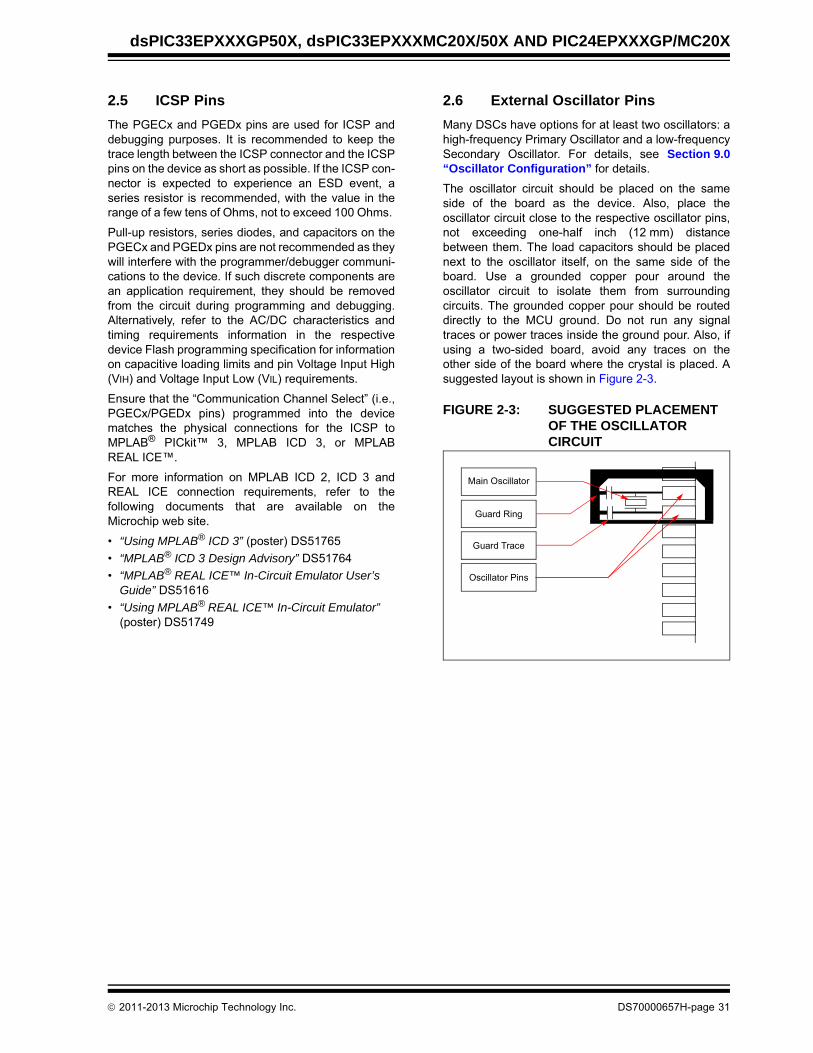
dsPIC33EPXXXGP50X, dsPIC33EPXXXMC20X/50X AND PIC24EPXXXGP/MC20X
2.5 ICSP Pins
The PGECx and PGEDx pins are used for ICSP anddebugging purposes. It is recommended to keep thetrace length between the ICSP connector and the ICSPpins on the device as short as possible. If the ICSP con-nector is expected to experience an ESD event, aseries resistor is recommended, with the value in therange of a few tens of Ohms, not to exceed 100 Ohms.
Pull-up resistors, series diodes, and capacitors on thePGECx and PGEDx pins are not recommended as theywill interfere with the programmer/debugger communi-cations to the device. If such discrete components arean application requirement, they should be removedfrom the circuit during programming and debugging.Alternatively, refer to the AC/DC characteristics andtiming requirements information in the respectivedevice Flash programming specification for informationon capacitive loading limits and pin Voltage Input High(VIH) and Voltage Input Low (VIL) requirements.
Ensure that the “Communication Channel Select” (i.e.,PGECx/PGEDx pins) programmed into the devicematches the physical connections for the ICSP toMPLAB® PICkit™ 3, MPLAB ICD 3, or MPLABREAL ICE™.
For more information on MPLAB ICD 2, ICD 3 andREAL ICE connection requirements, refer to thefollowing documents that are available on theMicrochip web site.
• “Using MPLAB® ICD 3” (poster) DS51765
• “MPLAB® ICD 3 Design Advisory” DS51764
• “MPLAB® REAL ICE™ In-Circuit Emulator User’s Guide” DS51616
• “Using MPLAB® REAL ICE™ In-Circuit Emulator” (poster) DS51749
2.6 External Oscillator Pins
Many DSCs have options for at least two oscillators: ahigh-frequency Primary Oscillator and a low-frequencySecondary Oscillator. For details, see Section 9.0“Oscillator Configuration” for details.
The oscillator circuit should be placed on the sameside of the board as the device. Also, place theoscillator circuit close to the respective oscillator pins,not exceeding one-half inch (12 mm) distancebetween them. The load capacitors should be placednext to the oscillator itself, on the same side of theboard. Use a grounded copper pour around theoscillator circuit to isolate them from surroundingcircuits. The grounded copper pour should be routeddirectly to the MCU ground. Do not run any signaltraces or power traces inside the ground pour. Also, ifusing a two-sided board, avoid any traces on theother side of the board where the crystal is placed. Asuggested layout is shown in Figure 2-3.
FIGURE 2-3: SUGGESTED PLACEMENT OF THE OSCILLATOR CIRCUIT
Main Oscillator
Guard Ring
Guard Trace
Oscillator Pins
2011-2013 Microchip Technology Inc. DS70000657H-page 31

dsPIC33EPXXXGP50X, dsPIC33EPXXXMC20X/50X AND PIC24EPXXXGP/MC20X
2.7 Oscillator Value Conditions on Device Start-up
If the PLL of the target device is enabled andconfigured for the device start-up oscillator, themaximum oscillator source frequency must be limitedto 3 MHz < FIN < 5.5 MHz to comply with device PLLstart-up conditions. This means that if the externaloscillator frequency is outside this range, theapplication must start-up in the FRC mode first. Thedefault PLL settings after a POR with an oscillatorfrequency outside this range will violate the deviceoperating speed.
Once the device powers up, the application firmwarecan initialize the PLL SFRs, CLKDIV and PLLFBD, to asuitable value, and then perform a clock switch to theOscillator + PLL clock source. Note that clock switchingmust be enabled in the device Configuration Word.
2.8 Unused I/Os
Unused I/O pins should be configured as outputs anddriven to a logic low state.
Alternatively, connect a 1k to 10k resistor between VSS
and unused pins, and drive the output to logic low.
2.9 Application Examples
• Induction heating• Uninterruptable Power Supplies (UPS)
• DC/AC inverters• Compressor motor control• Washing machine 3-phase motor control • BLDC motor control• Automotive HVAC, cooling fans, fuel pumps• Stepper motor control
• Audio and fluid sensor monitoring• Camera lens focus and stability control• Speech (playback, hands-free kits, answering
machines, VoIP)
• Consumer audio• Industrial and building control (security systems
and access control)• Barcode reading
• Networking: LAN switches, gateways• Data storage device management• Smart cards and smart card readers
Examples of typical application connections are shownin Figure 2-4 through Figure 2-8.
FIGURE 2-4: BOOST CONVERTER IMPLEMENTATION
IPFC
VOUTPUT
ADC Channel Op Amp/ ADC ChannelPWM
k1
k2
k3
FET
dsPIC33EP
VINPUT
Comparator Output
Driver
DS70000657H-page 32 2011-2013 Microchip Technology Inc.

dsPIC33EPXXXGP50X, dsPIC33EPXXXMC20X/50X AND PIC24EPXXXGP/MC20X
FIGURE 2-5: SINGLE-PHASE SYNCHRONOUS BUCK CONVERTER
FIGURE 2-6: MULTIPHASE SYNCHRONOUS BUCK CONVERTER
k1
Op Amp/Comparator
k2k7
PW
M
PW
M ADCChannel
ADCChannel
5V Output
I5V
12V Input
FETDriver
dsPIC33EP
k5
k4
k3
k6
k7
Op Amp/Comparator
Op Amp/Comparator
ADC Channel
Op Amp/Comparator
ADCChannel P
WM
PW
M
PWM
PWM
PW
MP
WM
3.3V Output12V Input
FETDriver
FETDriver
FETDriver
dsPIC33EP
2011-2013 Microchip Technology Inc. DS70000657H-page 33

dsPIC33EPXXXGP50X, dsPIC33EPXXXMC20X/50X AND PIC24EPXXXGP/MC20X
FIGURE 2-7: INTERLEAVED PFC
FIGURE 2-8: BEMF VOLTAGE MEASURED USING THE ADC MODULE
VAC
VOUT+
Op Amp/Comparator PWM ADCPWM
|VAC|
k4 k3
FET
dsPIC33EP
Driver
VOUT-
ADC Channel
FETDriver
Op Amp/
k1 k2
Comparator ChannelOp Amp/
Comparator
3-PhaseInverter
PWM3HPWM3LPWM2HPWM2LPWM1HPWM1L
FLTx Fault
BLDCdsPIC33EP/PIC24EP
AN3
AN4
AN5
AN2
Demand
Phase Terminal Voltage Feedback
R49 R41 R34 R36
R44
R52
DS70000657H-page 34 2011-2013 Microchip Technology Inc.

dsPIC33EPXXXGP50X, dsPIC33EPXXXMC20X/50X AND PIC24EPXXXGP/MC20X
3.0 CPU
The dsPIC33EPXXXGP50X, dsPIC33EPXXXMC20X/50X and PIC24EPXXXGP/MC20X CPU has a 16-bit(data) modified Harvard architecture with an enhancedinstruction set, including significant support for digitalsignal processing. The CPU has a 24-bit instructionword with a variable length opcode field. The ProgramCounter (PC) is 23 bits wide and addresses up to4M x 24 bits of user program memory space.
An instruction prefetch mechanism helps maintainthroughput and provides predictable execution. Mostinstructions execute in a single-cycle effective execu-tion rate, with the exception of instructions that changethe program flow, the double-word move (MOV.D)instruction, PSV accesses and the table instructions.Overhead-free program loop constructs are supportedusing the DO and REPEAT instructions, both of whichare interruptible at any point.
3.1 Registers
The dsPIC33EPXXXGP50X, dsPIC33EPXXXMC20X/50X and PIC24EPXXXGP/MC20X devices have six-teen, 16-bit working registers in the programmer’smodel. Each of the working registers can act as a data,address or address offset register. The 16th workingregister (W15) operates as a Software Stack Pointer forinterrupts and calls.
3.2 Instruction Set
The instruction set for dsPIC33EPXXXGP50X anddsPIC33EPXXXMC20X/50X devices has two classes ofinstructions: the MCU class of instructions and the DSPclass of instructions. The instruction set forPIC24EPXXXGP/MC20X devices has the MCU class ofinstructions only and does not support DSP instructions.These two instruction classes are seamlessly integratedinto the architecture and execute from a single executionunit. The instruction set includes many addressing modesand was designed for optimum C compiler efficiency.
3.3 Data Space Addressing
The base Data Space can be addressed as 64 Kbytes(32K words).
The Data Space includes two ranges of memory,referred to as X and Y data memory. Each memoryrange is accessible through its own independentAddress Generation Unit (AGU). The MCU class ofinstructions operates solely through the X memoryAGU, which accesses the entire memory map as onelinear Data Space. On dsPIC33EPXXXMC20X/50Xand dsPIC33EPXXXGP50X devices, certain DSPinstructions operate through the X and Y AGUs tosupport dual operand reads, which splits the dataaddress space into two parts. The X and Y Data Spaceshave memory locations that are device-specific, andare described further in the data memory maps inSection 4.2 “Data Address Space”.
The upper 32 Kbytes of the Data Space memory mapcan optionally be mapped into Program Space (PS) atany 32-Kbyte aligned program word boundary. TheProgram-to-Data Space mapping feature, known asProgram Space Visibility (PSV), lets any instructionaccess Program Space as if it were Data Space.Moreover, the Base Data Space address is used inconjunction with a Read or Write Page register (DSRPAGor DSWPAG) to form an Extended Data Space (EDS)address. The EDS can be addressed as 8M words or16 Mbytes. Refer to the “Data Memory” (DS70595) and“Program Memory” (DS70613) sections in the“dsPIC33/PIC24 Family Reference Manual” for moredetails on EDS, PSV and table accesses.
On the dsPIC33EPXXXMC20X/50X anddsPIC33EPXXXGP50X devices, overhead-free circularbuffers (Modulo Addressing) are supported in both Xand Y address spaces. The Modulo Addressingremoves the software boundary checking overhead forDSP algorithms. The X AGU Circular Addressing can beused with any of the MCU class of instructions. The XAGU also supports Bit-Reversed Addressing to greatlysimplify input or output data re-ordering for radix-2 FFTalgorithms. PIC24EPXXXGP/MC20X devices do notsupport Modulo and Bit-Reversed Addressing.
3.4 Addressing Modes
The CPU supports these addressing modes:
• Inherent (no operand)
• Relative
• Literal
• Memory Direct
• Register Direct
• Register Indirect
Each instruction is associated with a predefinedaddressing mode group, depending upon its functionalrequirements. As many as six addressing modes aresupported for each instruction.
Note 1: This data sheet summarizes thefeatures of the dsPIC33EPXXXGP50X,dsPIC33EPXXXMC20X/50X andPIC24EPXXXGP/MC20X families ofdevices. It is not intended to be acomprehensive reference source. To com-plement the information in this data sheet,refer to “CPU” (DS70359) in the“dsPIC33/PIC24 Family ReferenceManual”, which is available from theMicrochip web site (www.microchip.com).
2: Some registers and associated bitsdescribed in this section may not beavailable on all devices. Refer toSection 4.0 “Memory Organization” inthis data sheet for device-specific registerand bit information.
2011-2013 Microchip Technology Inc. DS70000657H-page 35
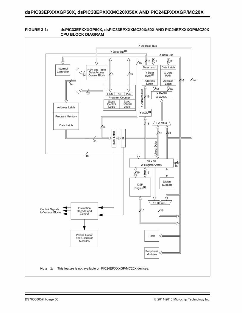
dsPIC33EPXXXGP50X, dsPIC33EPXXXMC20X/50X AND PIC24EPXXXGP/MC20X
FIGURE 3-1: dsPIC33EPXXXGP50X, dsPIC33EPXXXMC20X/50X AND PIC24EPXXXGP/MC20X CPU BLOCK DIAGRAM
InstructionDecode and
Control
16
PCL
16
Program Counter
16-Bit ALU
24
24
24
24
X Data Bus
PCU16
16 16
DivideSupport
Engine(1)DSP
RO
M L
atch
16
Y Data Bus(1)
EA MUX
X RAGUX WAGU
Y AGU(1)
16
24
16
16
16
16
16
16
16
8
InterruptController
PSV and TableData AccessControl Block
StackControlLogic
LoopControlLogic
Data LatchData Latch
Y DataRAM(1)
X DataRAM
AddressLatch
AddressLatch
16
Data Latch
16
16
16
X Address Bus
Y A
ddre
ss B
us
24
Lite
ral D
ata
Program Memory
Address Latch
Power, Resetand Oscillator
Control Signalsto Various Blocks
Ports
PeripheralModules
Note 1: This feature is not available on PIC24EPXXXGP/MC20X devices.
Modules
PCH
IR
16 x 16W Register Array
DS70000657H-page 36 2011-2013 Microchip Technology Inc.

dsPIC33EPXXXGP50X, dsPIC33EPXXXMC20X/50X AND PIC24EPXXXGP/MC20X
3.5 Programmer’s Model
The programmer’s model for thedsPIC33EPXXXGP50X, dsPIC33EPXXXMC20X/50Xand PIC24EPXXXGP/MC20X is shown in Figure 3-2.All registers in the programmer’s model are memorymapped and can be manipulated directly byinstructions. Table 3-1 lists a description of eachregister.
In addition to the registers contained in theprogrammer’s model, the dsPIC33EPXXXGP50X,dsPIC33EPXXXMC20X/50X and PIC24EPXXXGP/
MC20X devices contain control registers for ModuloAddressing (dsPIC33EPXXXMC20X/50X anddsPIC33EPXXXGP50X devices only), Bit-ReversedAddressing (dsPIC33EPXXXMC20X/50X anddsPIC33EPXXXGP50X devices only) and interrupts.These registers are described in subsequentsections of this document.
All registers associated with the programmer’s modelare memory mapped, as shown in Table 4-1.
TABLE 3-1: PROGRAMMER’S MODEL REGISTER DESCRIPTIONS
Register(s) Name Description
W0 through W15 Working Register Array
ACCA, ACCB 40-Bit DSP Accumulators
PC 23-Bit Program Counter
SR ALU and DSP Engine STATUS Register
SPLIM Stack Pointer Limit Value Register
TBLPAG Table Memory Page Address Register
DSRPAG Extended Data Space (EDS) Read Page Register
DSWPAG Extended Data Space (EDS) Write Page Register
RCOUNT REPEAT Loop Count Register
DCOUNT(1) DO Loop Count Register
DOSTARTH(1,2), DOSTARTL(1,2) DO Loop Start Address Register (High and Low)
DOENDH(1), DOENDL(1) DO Loop End Address Register (High and Low)
CORCON Contains DSP Engine, DO Loop Control and Trap Status bits
Note 1: This register is available on dsPIC33EPXXXMC20X/50X and dsPIC33EPXXXGP50X devices only.
2: The DOSTARTH and DOSTARTL registers are read-only.
2011-2013 Microchip Technology Inc. DS70000657H-page 37

dsPIC33EPXXXGP50X, dsPIC33EPXXXMC20X/50X AND PIC24EPXXXGP/MC20X
FIGURE 3-2: PROGRAMMER’S MODEL
N OV Z C
TBLPAG
PC23 PC0
7 0
D0D15
Program Counter
Data Table Page Address
STATUS Register
Working/AddressRegisters
DSP OperandRegisters
W0 (WREG)
W1
W2
W3
W4
W5
W6
W7
W8
W9
W10
W11
W12
W13
Frame Pointer/W14
Stack Pointer/W15
DSP AddressRegisters
AD39 AD0AD31
DSPAccumulators(1)
ACCA
ACCB
DSRPAG
9 0
RA
0
OA(1) OB(1) SA(1) SB(1)
RCOUNT15 0
Repeat Loop Counter
DCOUNT15 0
DO Loop Counter and Stack(1)
DOSTART
23 0
DO Loop Start Address and Stack(1)
0
DOEND DO Loop End Address and Stack(1)
IPL2 IPL1
SPLIM Stack Pointer Limit
AD15
23 0
SRL
IPL0
PUSH.s and POP.s Shadows
Nested DO Stack
0
0
OAB(1) SAB(1)
X Data Space Read Page Address
DA(1) DC
0
0
0
0
DSWPAG X Data Space Write Page Address
8 0
Note 1: This feature or bit is available on dsPIC33EPXXXMC20X/50X and dsPIC33EPXXXGP50X devices only.
CORCON15 0
CPU Core Control Register
DS70000657H-page 38 2011-2013 Microchip Technology Inc.

dsPIC33EPXXXGP50X, dsPIC33EPXXXMC20X/50X AND PIC24EPXXXGP/MC20X
3.6 CPU Resources
Many useful resources are provided on the main prod-uct page of the Microchip web site for the devices listedin this data sheet. This product page, which can beaccessed using this link, contains the latest updatesand additional information.
3.6.1 KEY RESOURCES
• “CPU” (DS70359) in the “dsPIC33/PIC24 Family Reference Manual”
• Code Samples
• Application Notes
• Software Libraries
• Webinars
• All related “dsPIC33/PIC24 Family Reference Manual” Sections
• Development Tools
Note: In the event you are not able to access theproduct page using the link above, enterthis URL in your browser:http://www.microchip.com/wwwproducts/Devices.aspx?dDocName=en555464
2011-2013 Microchip Technology Inc. DS70000657H-page 39
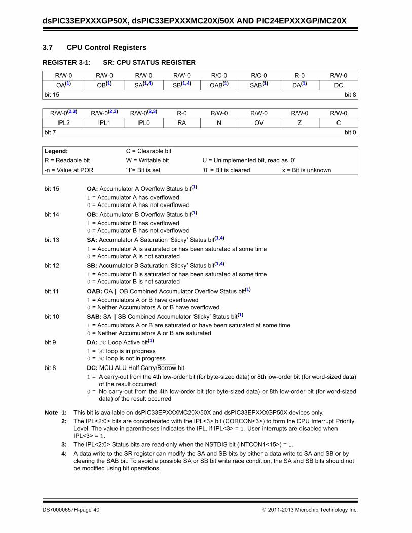
dsPIC33EPXXXGP50X, dsPIC33EPXXXMC20X/50X AND PIC24EPXXXGP/MC20X
3.7 CPU Control Registers
REGISTER 3-1: SR: CPU STATUS REGISTER
R/W-0 R/W-0 R/W-0 R/W-0 R/C-0 R/C-0 R-0 R/W-0
OA(1) OB(1) SA(1,4) SB(1,4) OAB(1) SAB(1) DA(1) DC
bit 15 bit 8
R/W-0(2,3) R/W-0(2,3) R/W-0(2,3) R-0 R/W-0 R/W-0 R/W-0 R/W-0
IPL2 IPL1 IPL0 RA N OV Z C
bit 7 bit 0
Legend: C = Clearable bit
R = Readable bit W = Writable bit U = Unimplemented bit, read as ‘0’
-n = Value at POR ‘1’= Bit is set ‘0’ = Bit is cleared x = Bit is unknown
bit 15 OA: Accumulator A Overflow Status bit(1)
1 = Accumulator A has overflowed0 = Accumulator A has not overflowed
bit 14 OB: Accumulator B Overflow Status bit(1)
1 = Accumulator B has overflowed0 = Accumulator B has not overflowed
bit 13 SA: Accumulator A Saturation ‘Sticky’ Status bit(1,4)
1 = Accumulator A is saturated or has been saturated at some time0 = Accumulator A is not saturated
bit 12 SB: Accumulator B Saturation ‘Sticky’ Status bit(1,4)
1 = Accumulator B is saturated or has been saturated at some time0 = Accumulator B is not saturated
bit 11 OAB: OA || OB Combined Accumulator Overflow Status bit(1)
1 = Accumulators A or B have overflowed0 = Neither Accumulators A or B have overflowed
bit 10 SAB: SA || SB Combined Accumulator ‘Sticky’ Status bit(1)
1 = Accumulators A or B are saturated or have been saturated at some time0 = Neither Accumulators A or B are saturated
bit 9 DA: DO Loop Active bit(1)
1 = DO loop is in progress0 = DO loop is not in progress
bit 8 DC: MCU ALU Half Carry/Borrow bit
1 = A carry-out from the 4th low-order bit (for byte-sized data) or 8th low-order bit (for word-sized data)of the result occurred
0 = No carry-out from the 4th low-order bit (for byte-sized data) or 8th low-order bit (for word-sizeddata) of the result occurred
Note 1: This bit is available on dsPIC33EPXXXMC20X/50X and dsPIC33EPXXXGP50X devices only.
2: The IPL<2:0> bits are concatenated with the IPL<3> bit (CORCON<3>) to form the CPU Interrupt Priority Level. The value in parentheses indicates the IPL, if IPL<3> = 1. User interrupts are disabled when IPL<3> = 1.
3: The IPL<2:0> Status bits are read-only when the NSTDIS bit (INTCON1<15>) = 1.
4: A data write to the SR register can modify the SA and SB bits by either a data write to SA and SB or by clearing the SAB bit. To avoid a possible SA or SB bit write race condition, the SA and SB bits should not be modified using bit operations.
DS70000657H-page 40 2011-2013 Microchip Technology Inc.

dsPIC33EPXXXGP50X, dsPIC33EPXXXMC20X/50X AND PIC24EPXXXGP/MC20X
bit 7-5 IPL<2:0>: CPU Interrupt Priority Level Status bits(2,3)
111 = CPU Interrupt Priority Level is 7 (15); user interrupts are disabled110 = CPU Interrupt Priority Level is 6 (14)101 = CPU Interrupt Priority Level is 5 (13)100 = CPU Interrupt Priority Level is 4 (12)011 = CPU Interrupt Priority Level is 3 (11)010 = CPU Interrupt Priority Level is 2 (10)001 = CPU Interrupt Priority Level is 1 (9)000 = CPU Interrupt Priority Level is 0 (8)
bit 4 RA: REPEAT Loop Active bit
1 = REPEAT loop in progress0 = REPEAT loop not in progress
bit 3 N: MCU ALU Negative bit
1 = Result was negative0 = Result was non-negative (zero or positive)
bit 2 OV: MCU ALU Overflow bit
This bit is used for signed arithmetic (2’s complement). It indicates an overflow of the magnitude thatcauses the sign bit to change state. 1 = Overflow occurred for signed arithmetic (in this arithmetic operation)0 = No overflow occurred
bit 1 Z: MCU ALU Zero bit
1 = An operation that affects the Z bit has set it at some time in the past0 = The most recent operation that affects the Z bit has cleared it (i.e., a non-zero result)
bit 0 C: MCU ALU Carry/Borrow bit
1 = A carry-out from the Most Significant bit of the result occurred0 = No carry-out from the Most Significant bit of the result occurred
REGISTER 3-1: SR: CPU STATUS REGISTER (CONTINUED)
Note 1: This bit is available on dsPIC33EPXXXMC20X/50X and dsPIC33EPXXXGP50X devices only.
2: The IPL<2:0> bits are concatenated with the IPL<3> bit (CORCON<3>) to form the CPU Interrupt Priority Level. The value in parentheses indicates the IPL, if IPL<3> = 1. User interrupts are disabled when IPL<3> = 1.
3: The IPL<2:0> Status bits are read-only when the NSTDIS bit (INTCON1<15>) = 1.
4: A data write to the SR register can modify the SA and SB bits by either a data write to SA and SB or by clearing the SAB bit. To avoid a possible SA or SB bit write race condition, the SA and SB bits should not be modified using bit operations.
2011-2013 Microchip Technology Inc. DS70000657H-page 41

dsPIC33EPXXXGP50X, dsPIC33EPXXXMC20X/50X AND PIC24EPXXXGP/MC20X
REGISTER 3-2: CORCON: CORE CONTROL REGISTER
R/W-0 U-0 R/W-0 R/W-0 R/W-0 R-0 R-0 R-0
VAR — US1(1) US0(1) EDT(1,2) DL2(1) DL1(1) DL0(1)
bit 15 bit 8
R/W-0 R/W-0 R/W-1 R/W-0 R/C-0 R-0 R/W-0 R/W-0
SATA(1) SATB(1) SATDW(1) ACCSAT(1) IPL3(3) SFA RND(1) IF(1)
bit 7 bit 0
Legend: C = Clearable bit
R = Readable bit W = Writable bit U = Unimplemented bit, read as ‘0’
-n = Value at POR ‘1’ = Bit is set ‘0’ = Bit is cleared x = Bit is unknown
bit 15 VAR: Variable Exception Processing Latency Control bit
1 = Variable exception processing latency is enabled0 = Fixed exception processing latency is enabled
bit 14 Unimplemented: Read as ‘0’
bit 13-12 US<1:0>: DSP Multiply Unsigned/Signed Control bits(1)
11 = Reserved10 = DSP engine multiplies are mixed-sign01 = DSP engine multiplies are unsigned 00 = DSP engine multiplies are signed
bit 11 EDT: Early DO Loop Termination Control bit(1,2)
1 = Terminates executing DO loop at end of current loop iteration0 = No effect
bit 10-8 DL<2:0>: DO Loop Nesting Level Status bits(1)
111 = 7 DO loops are active
•
•
•
001 = 1 DO loop is active000 = 0 DO loops are active
bit 7 SATA: ACCA Saturation Enable bit(1)
1 = Accumulator A saturation is enabled0 = Accumulator A saturation is disabled
bit 6 SATB: ACCB Saturation Enable bit(1)
1 = Accumulator B saturation is enabled0 = Accumulator B saturation is disabled
bit 5 SATDW: Data Space Write from DSP Engine Saturation Enable bit(1)
1 = Data Space write saturation is enabled0 = Data Space write saturation is disabled
bit 4 ACCSAT: Accumulator Saturation Mode Select bit(1)
1 = 9.31 saturation (super saturation)0 = 1.31 saturation (normal saturation)
bit 3 IPL3: CPU Interrupt Priority Level Status bit 3(3)
1 = CPU Interrupt Priority Level is greater than 70 = CPU Interrupt Priority Level is 7 or less
Note 1: This bit is available on dsPIC33EPXXXMC20X/50X and dsPIC33EPXXXGP50X devices only.
2: This bit is always read as ‘0’.
3: The IPL3 bit is concatenated with the IPL<2:0> bits (SR<7:5>) to form the CPU Interrupt Priority Level.
DS70000657H-page 42 2011-2013 Microchip Technology Inc.
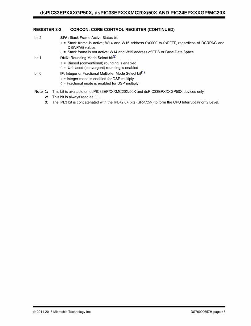
dsPIC33EPXXXGP50X, dsPIC33EPXXXMC20X/50X AND PIC24EPXXXGP/MC20X
bit 2 SFA: Stack Frame Active Status bit
1 = Stack frame is active; W14 and W15 address 0x0000 to 0xFFFF, regardless of DSRPAG andDSWPAG values
0 = Stack frame is not active; W14 and W15 address of EDS or Base Data Space
bit 1 RND: Rounding Mode Select bit(1)
1 = Biased (conventional) rounding is enabled0 = Unbiased (convergent) rounding is enabled
bit 0 IF: Integer or Fractional Multiplier Mode Select bit(1)
1 = Integer mode is enabled for DSP multiply0 = Fractional mode is enabled for DSP multiply
REGISTER 3-2: CORCON: CORE CONTROL REGISTER (CONTINUED)
Note 1: This bit is available on dsPIC33EPXXXMC20X/50X and dsPIC33EPXXXGP50X devices only.
2: This bit is always read as ‘0’.
3: The IPL3 bit is concatenated with the IPL<2:0> bits (SR<7:5>) to form the CPU Interrupt Priority Level.
2011-2013 Microchip Technology Inc. DS70000657H-page 43

dsPIC33EPXXXGP50X, dsPIC33EPXXXMC20X/50X AND PIC24EPXXXGP/MC20X
3.8 Arithmetic Logic Unit (ALU)
The dsPIC33EPXXXGP50X, dsPIC33EPXXXMC20X/50X and PIC24EPXXXGP/MC20X ALU is 16 bits wide,and is capable of addition, subtraction, bit shifts andlogic operations. Unless otherwise mentioned,arithmetic operations are two’s complement in nature.Depending on the operation, the ALU can affect thevalues of the Carry (C), Zero (Z), Negative (N),Overflow (OV) and Digit Carry (DC) Status bits in theSR register. The C and DC Status bits operate asBorrow and Digit Borrow bits, respectively, forsubtraction operations.
The ALU can perform 8-bit or 16-bit operations,depending on the mode of the instruction that is used.Data for the ALU operation can come from the Wregister array or data memory, depending on theaddressing mode of the instruction. Likewise, outputdata from the ALU can be written to the W register arrayor a data memory location.
Refer to the “16-bit MCU and DSC Programmer’sReference Manual” (DS70157) for information on theSR bits affected by each instruction.
The core CPU incorporates hardware support for bothmultiplication and division. This includes a dedicatedhardware multiplier and support hardware for 16-bitdivisor division.
3.8.1 MULTIPLIER
Using the high-speed 17-bit x 17-bit multiplier, the ALUsupports unsigned, signed, or mixed-sign operation inseveral MCU multiplication modes:
• 16-bit x 16-bit signed• 16-bit x 16-bit unsigned• 16-bit signed x 5-bit (literal) unsigned• 16-bit signed x 16-bit unsigned• 16-bit unsigned x 5-bit (literal) unsigned• 16-bit unsigned x 16-bit signed• 8-bit unsigned x 8-bit unsigned
3.8.2 DIVIDER
The divide block supports 32-bit/16-bit and 16-bit/16-bitsigned and unsigned integer divide operations with thefollowing data sizes:
• 32-bit signed/16-bit signed divide
• 32-bit unsigned/16-bit unsigned divide
• 16-bit signed/16-bit signed divide
• 16-bit unsigned/16-bit unsigned divide
The quotient for all divide instructions ends up in W0and the remainder in W1. The 16-bit signed andunsigned DIV instructions can specify any W registerfor both the 16-bit divisor (Wn) and any W register(aligned) pair (W(m + 1):Wm) for the 32-bit dividend.The divide algorithm takes one cycle per bit of divisor,so both 32-bit/16-bit and 16-bit/16-bit instructions takethe same number of cycles to execute.
3.9 DSP Engine (dsPIC33EPXXXMC20X/50X and dsPIC33EPXXXGP50X Devices Only)
The DSP engine consists of a high-speed 17-bit x17-bit multiplier, a 40-bit barrel shifter and a 40-bitadder/subtracter (with two target accumulators, roundand saturation logic).
The DSP engine can also perform inherent accumulator-to-accumulator operations that require no additionaldata. These instructions are ADD, SUB and NEG.
The DSP engine has options selected through bits inthe CPU Core Control register (CORCON), as listedbelow:
• Fractional or integer DSP multiply (IF)
• Signed, unsigned or mixed-sign DSP multiply (US)
• Conventional or convergent rounding (RND)
• Automatic saturation on/off for ACCA (SATA)
• Automatic saturation on/off for ACCB (SATB)
• Automatic saturation on/off for writes to data memory (SATDW)
• Accumulator Saturation mode selection (ACCSAT)
TABLE 3-2: DSP INSTRUCTIONS SUMMARY
InstructionAlgebraic Operation
ACC Write Back
CLR A = 0 Yes
ED A = (x – y)2 No
EDAC A = A + (x – y)2 No
MAC A = A + (x • y) Yes
MAC A = A + x2 No
MOVSAC No change in A Yes
MPY A = x • y No
MPY A = x2 No
MPY.N A = – x • y No
MSC A = A – x • y Yes
DS70000657H-page 44 2011-2013 Microchip Technology Inc.

dsPIC33EPXXXGP50X, dsPIC33EPXXXMC20X/50X AND PIC24EPXXXGP/MC20X
4.0 MEMORY ORGANIZATION
The dsPIC33EPXXXGP50X, dsPIC33EPXXXMC20X/50X and PIC24EPXXXGP/MC20X architecturefeatures separate program and data memory spaces,and buses. This architecture also allows the directaccess of program memory from the Data Space (DS)during code execution.
4.1 Program Address Space
The program address memory space of thedsPIC33EPXXXGP50X, dsPIC33EPXXXMC20X/50Xand PIC24EPXXXGP/MC20X devices is 4Minstructions. The space is addressable by a 24-bitvalue derived either from the 23-bit PC during programexecution, or from table operation or Data Spaceremapping, as described in Section 4.8 “InterfacingProgram and Data Memory Spaces”.
User application access to the program memory spaceis restricted to the lower half of the address range(0x000000 to 0x7FFFFF). The exception is the use ofTBLRD operations, which use TBLPAG<7> to readDevice ID sections of the configuration memory space.
The program memory maps, which are presented bydevice family and memory size, are shown inFigure 4-1 through Figure 4-5.
FIGURE 4-1: PROGRAM MEMORY MAP FOR dsPIC33EP32GP50X, dsPIC33EP32MC20X/50X AND PIC24EP32GP/MC20X DEVICES
Note: This data sheet summarizes thefeatures of the dsPIC33EPXXXGP50X,dsPIC33EPXXXMC20X/50X andPIC24EPXXXGP/MC20X families ofdevices. It is not intended to be acomprehensive reference source. To com-plement the information in this data sheet,refer to “Program Memory” (DS70613) inthe “dsPIC33/PIC24 Family ReferenceManual”, which is available from theMicrochip web site (www.microchip.com).
Reset Address
0x000000
0x000002
Write Latches
User ProgramFlash Memory
0x0057EC0x0057EA(11K instructions)
0x800000
0xFA00000xFA00020xFA0004
DEVID
0xFEFFFE0xFF0000
0xFFFFFE
0xF9FFFE
Unimplemented(Read ‘0’s)
GOTO Instruction
0x000004
Reserved
0x7FFFFE
Reserved
0x0002000x0001FEInterrupt Vector Table
Con
figu
ratio
n M
emor
y S
pace
Use
r M
emor
y S
pace
Flash ConfigurationBytes
0x0058000x0057FE
Reserved
0xFF0002
Note: Memory areas are not shown to scale.
0xFF0004
Reserved
0x800FF80x800FF6
0x8010000x800FFE
USERID
2011-2013 Microchip Technology Inc. DS70000657H-page 45

dsPIC33EPXXXGP50X, dsPIC33EPXXXMC20X/50X AND PIC24EPXXXGP/MC20X
FIGURE 4-2: PROGRAM MEMORY MAP FOR dsPIC33EP64GP50X, dsPIC33EP64MC20X/50X AND PIC24EP64GP/MC20X DEVICES
Reset Address
0x000000
0x000002
Write Latches
User ProgramFlash Memory
0x00AFEC0x00AFEA(22K instructions)
0x800000
0xFA00000xFA00020xFA0004
DEVID
0xFEFFFE0xFF0000
0xFFFFFE
0xF9FFFE
Unimplemented(Read ‘0’s)
GOTO Instruction
0x000004
Reserved
0x7FFFFE
Reserved
0x0002000x0001FEInterrupt Vector Table
Co
nfig
ura
tion
Me
mo
ry S
pace
Use
r M
em
ory
Spa
ce
Flash ConfigurationBytes
0x00B0000x00AFFE
Reserved
0xFF0002
Note: Memory areas are not shown to scale.
0xFF0004
Reserved
0x800FF80x800FF6
0x8010000x800FFE
USERID
DS70000657H-page 46 2011-2013 Microchip Technology Inc.

dsPIC33EPXXXGP50X, dsPIC33EPXXXMC20X/50X AND PIC24EPXXXGP/MC20X
FIGURE 4-3: PROGRAM MEMORY MAP FOR dsPIC33EP128GP50X, dsPIC33EP128MC20X/50X AND PIC24EP128GP/MC20X DEVICES
Reset Address
0x000000
0x000002
Write Latches
User ProgramFlash Memory
0x0157EC0x0157EA(44K instructions)
0x800000
0xFA00000xFA00020xFA0004
DEVID
0xFEFFFE0xFF0000
0xFFFFFE
0xF9FFFE
Unimplemented
(Read ‘0’s)
GOTO Instruction
0x000004
Reserved
0x7FFFFE
Reserved
0x0002000x0001FEInterrupt Vector Table
Con
figu
ratio
n M
emor
y S
pace
Use
r M
emor
y S
pace
Flash ConfigurationBytes
0x0158000x0157FE
Reserved
0xFF0002
Note: Memory areas are not shown to scale.
0xFF0004
Reserved
0x800FF80x800FF6
0x8010000x800FFE
USERID
2011-2013 Microchip Technology Inc. DS70000657H-page 47

dsPIC33EPXXXGP50X, dsPIC33EPXXXMC20X/50X AND PIC24EPXXXGP/MC20X
FIGURE 4-4: PROGRAM MEMORY MAP FOR dsPIC33EP256GP50X, dsPIC33EP256MC20X/50X AND PIC24EP256GP/MC20X DEVICES
Reset Address
0x000000
0x000002
Write Latches
User ProgramFlash Memory
0x02AFEC0x02AFEA(88K instructions)
0x800000
0xFA00000xFA00020xFA0004
DEVID
0xFEFFFE0xFF0000
0xFFFFFE
0xF9FFFE
Unimplemented
(Read ‘0’s)
GOTO Instruction
0x000004
Reserved
0x7FFFFE
Reserved
0x0002000x0001FEInterrupt Vector Table
Con
figur
atio
n M
emor
y S
pace
Use
r M
em
ory
Spa
ce
Flash ConfigurationBytes
0x02B0000x02AFFE
Reserved
0xFF0002
Note: Memory areas are not shown to scale.
0xFF0004
Reserved
0x800FF80x800FF6
0x8010000x800FFE
USERID
DS70000657H-page 48 2011-2013 Microchip Technology Inc.

dsPIC33EPXXXGP50X, dsPIC33EPXXXMC20X/50X AND PIC24EPXXXGP/MC20X
FIGURE 4-5: PROGRAM MEMORY MAP FOR dsPIC33EP512GP50X, dsPIC33EP512MC20X/50X AND PIC24EP512GP/MC20X DEVICES
Reset Address
0x000000
0x000002
Write Latches
User ProgramFlash Memory
0x0557EC0x0557EA(175K instructions)
0x800000
0xFA00000xFA00020xFA0004
DEVID
0xFEFFFE0xFF0000
0xFFFFFE
0xF9FFFE
Unimplemented
(Read ‘0’s)
GOTO Instruction
0x000004
Reserved
0x7FFFFE
Reserved
0x0002000x0001FEInterrupt Vector Table
Con
figur
atio
n M
emor
y S
pace
Use
r M
em
ory
Spa
ce
Flash ConfigurationBytes
0x0558000x0557FE
Reserved
0xFF0002
Note: Memory areas are not shown to scale.
0xFF0004
Reserved
0x800FF80x800FF6
0x8010000x800FFE
USERID
2011-2013 Microchip Technology Inc. DS70000657H-page 49

dsPIC33EPXXXGP50X, dsPIC33EPXXXMC20X/50X AND PIC24EPXXXGP/MC20X
4.1.1 PROGRAM MEMORY ORGANIZATION
The program memory space is organized in word-addressable blocks. Although it is treated as 24 bitswide, it is more appropriate to think of each address ofthe program memory as a lower and upper word, withthe upper byte of the upper word being unimplemented.The lower word always has an even address, while theupper word has an odd address (Figure 4-6).
Program memory addresses are always word-alignedon the lower word and addresses are incremented, ordecremented by two, during code execution. Thisarrangement provides compatibility with data memoryspace addressing and makes data in the programmemory space accessible.
4.1.2 INTERRUPT AND TRAP VECTORS
All dsPIC33EPXXXGP50X, dsPIC33EPXXXMC20X/50X and PIC24EPXXXGP/MC20X devices reserve theaddresses between 0x000000 and 0x000200 for hard-coded program execution vectors. A hardware Resetvector is provided to redirect code execution from thedefault value of the PC on device Reset to the actualstart of code. A GOTO instruction is programmed by theuser application at address, 0x000000, of Flashmemory, with the actual address for the start of code ataddress, 0x000002, of Flash memory.
A more detailed discussion of the Interrupt VectorTables (IVTs) is provided in Section 7.1 “InterruptVector Table”.
FIGURE 4-6: PROGRAM MEMORY ORGANIZATION
0816
PC Address
0x000000
0x000002
0x0000040x000006
23
0000000000000000
0000000000000000
Program Memory‘Phantom’ Byte
(read as ‘0’)
least significant wordmost significant word
Instruction Width
0x000001
0x000003
0x0000050x000007
mswAddress (lsw Address)
DS70000657H-page 50 2011-2013 Microchip Technology Inc.

dsPIC33EPXXXGP50X, dsPIC33EPXXXMC20X/50X AND PIC24EPXXXGP/MC20X
4.2 Data Address Space
The dsPIC33EPXXXGP50X, dsPIC33EPXXXMC20X/50X and PIC24EPXXXGP/MC20X CPU has a separate16-bit-wide data memory space. The Data Space isaccessed using separate Address Generation Units(AGUs) for read and write operations. The datamemory maps, which are presented by device familyand memory size, are shown in Figure 4-7 throughFigure 4-16.
All Effective Addresses (EAs) in the data memory spaceare 16 bits wide and point to bytes within the DataSpace. This arrangement gives a base Data Spaceaddress range of 64 Kbytes (32K words).
The base Data Space address is used in conjunctionwith a Read or Write Page register (DSRPAG orDSWPAG) to form an Extended Data Space, which hasa total address range of 16 Mbytes.
dsPIC33EPXXXGP50X, dsPIC33EPXXXMC20X/50Xand PIC24EPXXXGP/MC20X devices implement up to52 Kbytes of data memory (4 Kbytes of data memoryfor Special Function Registers and up to 48 Kbytes ofdata memory for RAM). If an EA points to a locationoutside of this area, an all-zero word or byte is returned.
4.2.1 DATA SPACE WIDTH
The data memory space is organized in byte-addressable, 16-bit-wide blocks. Data is aligned in datamemory and registers as 16-bit words, but all DataSpace EAs resolve to bytes. The Least SignificantBytes (LSBs) of each word have even addresses, whilethe Most Significant Bytes (MSBs) have oddaddresses.
4.2.2 DATA MEMORY ORGANIZATION AND ALIGNMENT
To maintain backward compatibility with PIC® MCUdevices and improve Data Space memoryusage efficiency, the dsPIC33EPXXXGP50X,dsPIC33EPXXXMC20X/50X and PIC24EPXXXGP/MC20X instruction set supports both word and byteoperations. As a consequence of byte accessibility, allEffective Address calculations are internally scaled tostep through word-aligned memory. For example, thecore recognizes that Post-Modified Register IndirectAddressing mode [Ws++] results in a value of Ws + 1for byte operations and Ws + 2 for word operations.
A data byte read, reads the complete word thatcontains the byte, using the LSb of any EA to determinewhich byte to select. The selected byte is placed ontothe LSB of the data path. That is, data memory andregisters are organized as two parallel, byte-wideentities with shared (word) address decode butseparate write lines. Data byte writes only write to thecorresponding side of the array or register that matchesthe byte address.
All word accesses must be aligned to an even address.Misaligned word data fetches are not supported, socare must be taken when mixing byte and wordoperations, or translating from 8-bit MCU code. If amisaligned read or write is attempted, an address errortrap is generated. If the error occurred on a read, theinstruction underway is completed. If the error occurredon a write, the instruction is executed but the write doesnot occur. In either case, a trap is then executed,allowing the system and/or user application to examinethe machine state prior to execution of the addressFault.
All byte loads into any W register are loaded into theLSB. The MSB is not modified.
A Sign-Extend (SE) instruction is provided to allow userapplications to translate 8-bit signed data to 16-bitsigned values. Alternatively, for 16-bit unsigned data,user applications can clear the MSB of any W registerby executing a Zero-Extend (ZE) instruction on theappropriate address.
4.2.3 SFR SPACE
The first 4 Kbytes of the Near Data Space, from 0x0000to 0x0FFF, is primarily occupied by Special FunctionRegisters (SFRs). These are used by thedsPIC33EPXXXGP50X, dsPIC33EPXXXMC20X/50Xand PIC24EPXXXGP/MC20X core and peripheralmodules for controlling the operation of the device.
SFRs are distributed among the modules that theycontrol and are generally grouped together by module.Much of the SFR space contains unused addresses;these are read as ‘0’.
4.2.4 NEAR DATA SPACE
The 8-Kbyte area, between 0x0000 and 0x1FFF, isreferred to as the Near Data Space. Locations in thisspace are directly addressable through a 13-bit abso-lute address field within all memory direct instructions.Additionally, the whole Data Space is addressableusing MOV instructions, which support Memory DirectAddressing mode with a 16-bit address field, or byusing Indirect Addressing mode using a workingregister as an Address Pointer.
Note: The actual set of peripheral features andinterrupts varies by the device. Refer tothe corresponding device tables andpinout diagrams for device-specificinformation.
2011-2013 Microchip Technology Inc. DS70000657H-page 51

dsPIC33EPXXXGP50X, dsPIC33EPXXXMC20X/50X AND PIC24EPXXXGP/MC20X
FIGURE 4-7: DATA MEMORY MAP FOR dsPIC33EP32MC20X/50X AND dsPIC33EP32GP50X DEVICES
0x0000
0x0FFE
0x17FE
0xFFFE
LSBAddress16 Bits
LSBMSB
MSBAddress
0x0001
0x0FFF
0x17FF
0xFFFF
OptionallyMappedinto ProgramMemory Space
0x1FFF 0x1FFE
0x1001 0x1000
0x1801 0x1800
4-KbyteSFR Space
4-Kbyte
SRAM Space
0x20000x2001
Data SpaceNear8-Kbyte
SFR Space
X Data RAM (X)
X DataUnimplemented (X)
0x80000x8001
Note: Memory areas are not shown to scale.
(PSV)
Y Data RAM (Y)
DS70000657H-page 52 2011-2013 Microchip Technology Inc.

dsPIC33EPXXXGP50X, dsPIC33EPXXXMC20X/50X AND PIC24EPXXXGP/MC20X
FIGURE 4-8: DATA MEMORY MAP FOR dsPIC33EP64MC20X/50X AND dsPIC33EP64GP50X DEVICES
0x0000
0x0FFE
0x1FFE
0xFFFE
LSBAddress16 Bits
LSBMSB
MSBAddress
0x0001
0x0FFF
0x1FFF
0xFFFF
OptionallyMappedinto ProgramMemory Space
0x2FFF 0x2FFE
0x1001 0x1000
0x2001 0x2000
4-KbyteSFR Space
8-KbyteSRAM Space
0x30000x3001
Data SpaceNear8-Kbyte
SFR Space
X Data RAM (X)
X DataUnimplemented (X)
0x80000x8001
Note: Memory areas are not shown to scale.
(PSV)
Y Data RAM (Y)
2011-2013 Microchip Technology Inc. DS70000657H-page 53

dsPIC33EPXXXGP50X, dsPIC33EPXXXMC20X/50X AND PIC24EPXXXGP/MC20X
FIGURE 4-9: DATA MEMORY MAP FOR dsPIC33EP128MC20X/50X AND dsPIC33EP128GP50X DEVICES
0x0000
0x0FFE
0x2FFE
0xFFFE
LSBAddress16 Bits
LSBMSB
MSBAddress
0x0001
0x0FFF
0x2FFF
0xFFFF
OptionallyMappedinto ProgramMemory Space
0x4FFF 0x4FFE
0x1001 0x1000
0x3001 0x3000
4-KbyteSFR Space
16-Kbyte
SRAM Space
0x50000x5001
Data SpaceNear8-Kbyte
SFR Space
X Data RAM (X)
X DataUnimplemented (X)
0x80000x8001
Note: Memory areas are not shown to scale.
(PSV)
0x1FFE0x1FFF0x2001 0x2000
Y Data RAM (Y)
DS70000657H-page 54 2011-2013 Microchip Technology Inc.
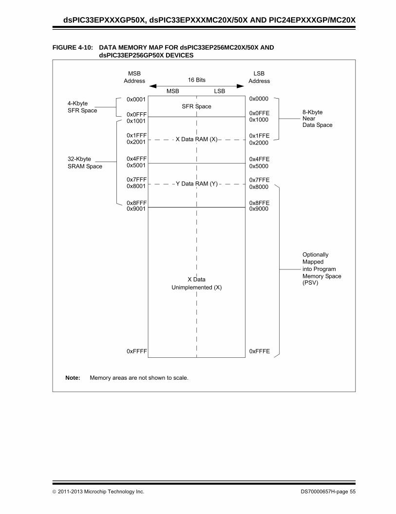
dsPIC33EPXXXGP50X, dsPIC33EPXXXMC20X/50X AND PIC24EPXXXGP/MC20X
FIGURE 4-10: DATA MEMORY MAP FOR dsPIC33EP256MC20X/50X AND dsPIC33EP256GP50X DEVICES
0x0000
0x0FFE
0x4FFE
0xFFFE
LSBAddress16 Bits
LSBMSB
MSBAddress
0x0001
0x0FFF
0x4FFF
0xFFFF
OptionallyMappedinto ProgramMemory Space
0x8FFF 0x8FFE
0x1001 0x1000
0x5001 0x5000
4-KbyteSFR Space
32-KbyteSRAM Space
0x90000x9001
Data SpaceNear8-Kbyte
SFR Space
X Data RAM (X)
X DataUnimplemented (X)
Y Data RAM (Y)
Note: Memory areas are not shown to scale.
(PSV)
0x1FFE0x1FFF0x2001 0x2000
0x7FFE0x7FFF0x8001 0x8000
2011-2013 Microchip Technology Inc. DS70000657H-page 55

dsPIC33EPXXXGP50X, dsPIC33EPXXXMC20X/50X AND PIC24EPXXXGP/MC20X
FIGURE 4-11: DATA MEMORY MAP FOR dsPIC33EP512MC20X/50X AND dsPIC33EP512GP50X DEVICES
0x0000
0x0FFE
0x7FFE
0xFFFE
LSBAddress16 Bits
LSBMSB
MSBAddress
0x0001
0x0FFF
0x7FFF
0xFFFF
OptionallyMappedinto ProgramMemory Space
0xEFFF 0xEFFE
0x1001 0x1000
0x8001 0x8000
4-KbyteSFR Space
48-KbyteSRAM Space
0xD0000xD001
Data SpaceNear8-Kbyte
SFR Space
X Data RAM (X)
X DataUnimplemented (X)
Note: Memory areas are not shown to scale.
(PSV)
0x1FFE0x1FFF0x2001 0x2000
0x8FFE0x8FFF0x9001 0x9000
Y Data RAM (Y)
DS70000657H-page 56 2011-2013 Microchip Technology Inc.

dsPIC33EPXXXGP50X, dsPIC33EPXXXMC20X/50X AND PIC24EPXXXGP/MC20X
FIGURE 4-12: DATA MEMORY MAP FOR PIC24EP32GP/MC20X/50X DEVICES
0x0000
0x0FFE
0xFFFE
LSBAddress16 Bits
LSBMSB
MSBAddress
0x0001
0x0FFF
0xFFFF
OptionallyMappedinto ProgramMemory Space
0x1FFF 0x1FFE
0x1001 0x1000
4-KbyteSFR Space
4-KbyteSRAM Space
0x20000x2001
Data SpaceNear8-Kbyte
SFR Space
X Data RAM (X)
X DataUnimplemented (X)
0x80000x8001
Note: Memory areas are not shown to scale.
(PSV)
2011-2013 Microchip Technology Inc. DS70000657H-page 57
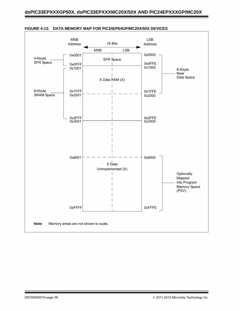
dsPIC33EPXXXGP50X, dsPIC33EPXXXMC20X/50X AND PIC24EPXXXGP/MC20X
FIGURE 4-13: DATA MEMORY MAP FOR PIC24EP64GP/MC20X/50X DEVICES
0x0000
0x0FFE
0x1FFE
0xFFFE
LSBAddress16 Bits
LSBMSB
MSBAddress
0x0001
0x0FFF
0x1FFF
0xFFFF
OptionallyMappedinto ProgramMemory Space
0x2FFF 0x2FFE
0x1001 0x1000
0x2001 0x2000
4-KbyteSFR Space
8-KbyteSRAM Space
0x30000x3001
Data SpaceNear8-Kbyte
SFR Space
X Data RAM (X)
X DataUnimplemented (X)
0x80000x8001
Note: Memory areas are not shown to scale.
(PSV)
DS70000657H-page 58 2011-2013 Microchip Technology Inc.

dsPIC33EPXXXGP50X, dsPIC33EPXXXMC20X/50X AND PIC24EPXXXGP/MC20X
FIGURE 4-14: DATA MEMORY MAP FOR PIC24EP128GP/MC20X/50X DEVICES
0x0000
0x0FFE
0xFFFE
LSBAddress16 Bits
LSBMSB
MSBAddress
0x0001
0x0FFF
0xFFFF
OptionallyMappedinto ProgramMemory Space
0x4FFF 0x4FFE
0x1001 0x1000
4-KbyteSFR Space
16-KbyteSRAM Space
0x50000x5001
Data SpaceNear8-Kbyte
SFR Space
X Data RAM (X)
X DataUnimplemented (X)
0x80000x8001
Note: Memory areas are not shown to scale.
(PSV)
0x1FFE0x1FFF0x2001 0x2000
2011-2013 Microchip Technology Inc. DS70000657H-page 59

dsPIC33EPXXXGP50X, dsPIC33EPXXXMC20X/50X AND PIC24EPXXXGP/MC20X
FIGURE 4-15: DATA MEMORY MAP FOR PIC24EP256GP/MC20X/50X DEVICES
0x0000
0x0FFE
0xFFFE
LSBAddress16 Bits
LSBMSB
MSBAddress
0x0001
0x0FFF
0xFFFF
OptionallyMappedinto ProgramMemory Space
0x8FFF 0x8FFE
0x1001 0x1000
4-KbyteSFR Space
32-KbyteSRAM Space
0x90000x9001
Data SpaceNear8-Kbyte
SFR Space
X Data RAM (X)
X DataUnimplemented (X)
Note: Memory areas are not shown to scale.
(PSV)
0x1FFE0x1FFF0x2001 0x2000
0x7FFE0x7FFF0x8001 0x8000
DS70000657H-page 60 2011-2013 Microchip Technology Inc.

dsPIC33EPXXXGP50X, dsPIC33EPXXXMC20X/50X AND PIC24EPXXXGP/MC20X
FIGURE 4-16: DATA MEMORY MAP FOR PIC24EP512GP/MC20X/50X DEVICES
0x0000
0x0FFE
0xFFFE
LSBAddress16 Bits
LSBMSB
MSBAddress
0x0001
0x0FFF
0xFFFF
OptionallyMappedinto ProgramMemory Space
0xEFFF 0xEFFE
0x1001 0x1000
4-KbyteSFR Space
48-KbyteSRAM Space
0xD0000xD001
Data SpaceNear8-Kbyte
SFR Space
X Data RAM (X)
X DataUnimplemented (X)
Note: Memory areas are not shown to scale.
(PSV)
0x1FFE0x1FFF0x2001 0x2000
0x7FFE0x7FFF0x8001 0x8000
2011-2013 Microchip Technology Inc. DS70000657H-page 61

dsPIC33EPXXXGP50X, dsPIC33EPXXXMC20X/50X AND PIC24EPXXXGP/MC20X
4.2.5 X AND Y DATA SPACES
The dsPIC33EPXXXMC20X/50X anddsPIC33EPXXXGP50X core has two Data Spaces,X and Y. These Data Spaces can be considered eitherseparate (for some DSP instructions) or as one unifiedlinear address range (for MCU instructions). The DataSpaces are accessed using two Address GenerationUnits (AGUs) and separate data paths. This featureallows certain instructions to concurrently fetch twowords from RAM, thereby enabling efficient executionof DSP algorithms, such as Finite Impulse Response(FIR) filtering and Fast Fourier Transform (FFT).
The X Data Space is used by all instructions andsupports all addressing modes. X Data Space hasseparate read and write data buses. The X read databus is the read data path for all instructions that viewData Space as combined X and Y address space. It isalso the X data prefetch path for the dual operand DSPinstructions (MAC class).
The Y Data Space is used in concert with the X DataSpace by the MAC class of instructions (CLR, ED,EDAC, MAC, MOVSAC, MPY, MPY.N and MSC) to providetwo concurrent data read paths.
Both the X and Y Data Spaces support ModuloAddressing mode for all instructions, subject toaddressing mode restrictions. Bit-Reversed Addressingmode is only supported for writes to X Data Space.Modulo Addressing and Bit-Reversed Addressing arenot present in PIC24EPXXXGP/MC20X devices.
All data memory writes, including in DSP instructions,view Data Space as combined X and Y address space.The boundary between the X and Y Data Spaces isdevice-dependent and is not user-programmable.
4.3 Memory Resources
Many useful resources are provided on the main prod-uct page of the Microchip web site for the devices listedin this data sheet. This product page, which can beaccessed using this link, contains the latest updatesand additional information.
4.3.1 KEY RESOURCES
• “Program Memory” (DS70613) in the “dsPIC33/PIC24 Family Reference Manual”
• Code Samples
• Application Notes
• Software Libraries
• Webinars
• All Related “dsPIC33/PIC24 Family Reference Manual” Sections
• Development Tools
Note: In the event you are not able to access theproduct page using the link above, enterthis URL in your browser:http://www.microchip.com/wwwproducts/Devices.aspx?dDocName=en555464
DS70000657H-page 62 2011-2013 Microchip Technology Inc.
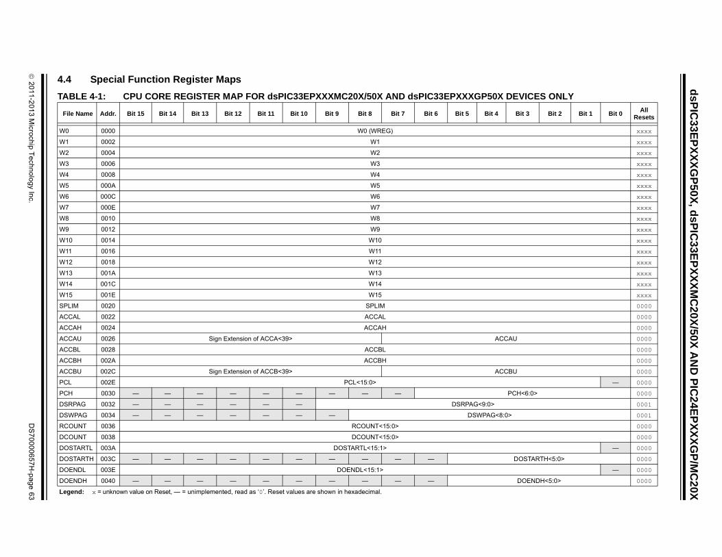
2
01
1-2
01
3 M
icroch
ip T
ech
no
log
y Inc.
DS
70
00
06
57
H-p
ag
e 6
3
ds
PIC
33E
PX
XX
GP
50X
, ds
PIC
33E
PX
XX
MC
20X
/50X
AN
D P
IC2
4EP
XX
XG
P/M
C2
0X
4.4
TA EVICES ONLY
Fi Bit 3 Bit 2 Bit 1 Bit 0All
Resets
W0 xxxx
W1 xxxx
W2 xxxx
W3 xxxx
W4 xxxx
W5 xxxx
W6 xxxx
W7 xxxx
W8 xxxx
W9 xxxx
W1 xxxx
W1 xxxx
W1 xxxx
W1 xxxx
W1 xxxx
W1 xxxx
SP 0000
AC 0000
AC 0000
AC U 0000
AC 0000
AC 0000
AC U 0000
PC — 0000
PC CH<6:0> 0000
DS 0001
DS 0001
RC 0000
DC 0000
DO — 0000
DO DOSTARTH<5:0> 0000
DO — 0000
DO DOENDH<5:0> 0000
Leg
Special Function Register Maps
BLE 4-1: CPU CORE REGISTER MAP FOR dsPIC33EPXXXMC20X/50X AND dsPIC33EPXXXGP50X D
le Name Addr. Bit 15 Bit 14 Bit 13 Bit 12 Bit 11 Bit 10 Bit 9 Bit 8 Bit 7 Bit 6 Bit 5 Bit 4
0000 W0 (WREG)
0002 W1
0004 W2
0006 W3
0008 W4
000A W5
000C W6
000E W7
0010 W8
0012 W9
0 0014 W10
1 0016 W11
2 0018 W12
3 001A W13
4 001C W14
5 001E W15
LIM 0020 SPLIM
CAL 0022 ACCAL
CAH 0024 ACCAH
CAU 0026 Sign Extension of ACCA<39> ACCA
CBL 0028 ACCBL
CBH 002A ACCBH
CBU 002C Sign Extension of ACCB<39> ACCB
L 002E PCL<15:0>
H 0030 — — — — — — — — — P
RPAG 0032 — — — — — — DSRPAG<9:0>
WPAG 0034 — — — — — — — DSWPAG<8:0>
OUNT 0036 RCOUNT<15:0>
OUNT 0038 DCOUNT<15:0>
STARTL 003A DOSTARTL<15:1>
STARTH 003C — — — — — — — — — —
ENDL 003E DOENDL<15:1>
ENDH 0040 — — — — — — — — — —
end: x = unknown value on Reset, — = unimplemented, read as ‘0’. Reset values are shown in hexadecimal.

ds
PIC
33E
PX
XX
GP
50X
, dsP
IC33
EP
XX
XM
C20
X/5
0X A
ND
PIC
24E
PX
XX
GP
/MC
20X
DS
70
00
06
57
H-p
ag
e 6
4
20
11
-20
13
Micro
chip
Te
chn
olo
gy In
c.
N OV Z C 0000
AT IPL3 SFA RND IF 0020
XWM<3:0> 0000
— 0000
— 0001
— 0000
— 0001
0000
0000
LPAG<7:0> 0000
0000
X DEVICES ONLY (CONTINUED)
4 Bit 3 Bit 2 Bit 1 Bit 0All
Resets
SR 0042 OA OB SA SB OAB SAB DA DC IPL2 IPL1 IPL0 RA
CORCON 0044 VAR — US<1:0> EDT DL<2:0> SATA SATB SATDW ACCS
MODCON 0046 XMODEN YMODEN — — BWM<3:0> YWM<3:0>
XMODSRT 0048 XMODSRT<15:0>
XMODEND 004A XMODEND<15:0>
YMODSRT 004C YMODSRT<15:0>
YMODEND 004E YMODEND<15:0>
XBREV 0050 BREN XBREV<14:0>
DISICNT 0052 — — DISICNT<13:0>
TBLPAG 0054 — — — — — — — — TB
MSTRPR 0058 MSTRPR<15:0>
TABLE 4-1: CPU CORE REGISTER MAP FOR dsPIC33EPXXXMC20X/50X AND dsPIC33EPXXXGP50
File Name Addr. Bit 15 Bit 14 Bit 13 Bit 12 Bit 11 Bit 10 Bit 9 Bit 8 Bit 7 Bit 6 Bit 5 Bit
Legend: x = unknown value on Reset, — = unimplemented, read as ‘0’. Reset values are shown in hexadecimal.

2
01
1-2
01
3 M
icroch
ip T
ech
no
log
y Inc.
DS
70
00
06
57
H-p
ag
e 6
5
ds
PIC
33E
PX
XX
GP
50X
, ds
PIC
33E
PX
XX
MC
20X
/50X
AN
D P
IC2
4EP
XX
XG
P/M
C2
0X
TA
NBit 3 Bit 2 Bit 1 Bit 0
All Resets
W0 xxxx
W1 xxxx
W2 xxxx
W3 xxxx
W4 xxxx
W5 xxxx
W6 xxxx
W7 xxxx
W8 xxxx
W9 xxxx
W1 xxxx
W1 xxxx
W1 xxxx
W1 xxxx
W1 xxxx
W1 xxxx
SP 0000
PC — 0000
PC CH<6:0> 0000
DS 0001
DS 0001
RC 0000
SR N OV Z C 0000
CO IPL3 SFA — — 0020
DI 0000
TB <7:0> 0000
MS 0000
Le
BLE 4-2: CPU CORE REGISTER MAP FOR PIC24EPXXXGP/MC20X DEVICES ONLY
File ame
Addr. Bit 15 Bit 14 Bit 13 Bit 12 Bit 11 Bit 10 Bit 9 Bit 8 Bit 7 Bit 6 Bit 5 Bit 4
0000 W0 (WREG)
0002 W1
0004 W2
0006 W3
0008 W4
000A W5
000C W6
000E W7
0010 W8
0012 W9
0 0014 W10
1 0016 W11
2 0018 W12
3 001A W13
4 001C W14
5 001E W15
LIM 0020 SPLIM<15:0>
L 002E PCL<15:1>
H 0030 — — — — — — — — — P
RPAG 0032 — — — — — — DSRPAG<9:0>
WPAG 0034 — — — — — — — DSWPAG<8:0>
OUNT 0036 RCOUNT<15:0>
0042 — — — — — — — DC IPL2 IPL1 IPL0 RA
RCON 0044 VAR — — — — — — — — — — —
SICNT 0052 — — DISICNT<13:0>
LPAG 0054 — — — — — — — — TBLPAG
TRPR 0058 MSTRPR<15:0>
gend: x = unknown value on Reset, — = unimplemented, read as ‘0’. Reset values are shown in hexadecimal.

ds
PIC
33E
PX
XX
GP
50X
, dsP
IC33
EP
XX
XM
C20
X/5
0X A
ND
PIC
24E
PX
XX
GP
/MC
20X
DS
70
00
06
57
H-p
ag
e 6
6
20
11
-20
13
Micro
chip
Te
chn
olo
gy In
c.
Bit 3 Bit 2 Bit 1 Bit 0All
Resets
T1IF OC1IF IC1IF INT0IF 0000
CNIF CMIF MI2C1IF SI2C1IF 0000
— — SPI2IF SPI2EIF 0000
— MI2C2IF SI2C2IF — 0000
RCIF U2EIF U1EIF — 0000
— — — — 0000
TG0IF PTGWDTIF PTGSTEPIF — 0000
T1IE OC1IE IC1IE INT0IE 0000
CNIE CMIE MI2C1IE SI2C1IE 0000
— — SPI2IE SPI2EIE 0000
— MI2C2IE SI2C2IE — 0000
RCIE U2EIE U1EIE — 0000
— — — — 0000
TG0IE PTGWDTIE PTGSTEPIE — 0000
— INT0IP<2:0> 4444
— DMA0IP<2:0> 4444
— T3IP<2:0> 4444
— U1TXIP<2:0> 0444
— SI2C1IP<2:0> 4444
— INT1IP<2:0> 0004
— DMA2IP<2:0> 4444
— T5IP<2:0> 4444
— SPI2EIP<2:0> 0044
— DMA3IP<2:0> 0444
— — — — 0440
— — — — 4440
— — — — 0040
— — — — 4400
— — — — 4440
— PTG1IP<2:0> 0444
DRERR STKERR OSCFAIL — 0000
— INT2EP INT1EP INT0EP 8000
— — — — 0000
— — — SGHT 0000
7:0> 0000
TABLE 4-3: INTERRUPT CONTROLLER REGISTER MAP FOR PIC24EPXXXGP20X DEVICES ONLY
File Name
Addr. Bit 15 Bit 14 Bit 13 Bit 12 Bit 11 Bit 10 Bit 9 Bit 8 Bit 7 Bit 6 Bit 5 Bit 4
IFS0 0800 — DMA1IF AD1IF U1TXIF U1RXIF SPI1IF SPI1EIF T3IF T2IF OC2IF IC2IF DMA0IF
IFS1 0802 U2TXIF U2RXIF INT2IF T5IF T4IF OC4IF OC3IF DMA2IF — — — INT1IF
IFS2 0804 — — — — — — — — — IC4IF IC3IF DMA3IF
IFS3 0806 — — — — — — — — — — — —
IFS4 0808 — — CTMUIF — — — — — — — — — C
IFS8 0810 JTAGIF ICDIF — — — — — — — — — —
IFS9 0812 — — — — — — — — — PTG3IF PTG2IF PTG1IF P
IEC0 0820 — DMA1IE AD1IE U1TXIE U1RXIE SPI1IE SPI1EIE T3IE T2IE OC2IE IC2IE DMA0IE
IEC1 0822 U2TXIE U2RXIE INT2IE T5IE T4IE OC4IE OC3IE DMA2IE — — — INT1IE
IEC2 0824 — — — — — — — — — IC4IE IC3IE DMA3IE
IEC3 0826 — — — — — — — — — — — —
IEC4 0828 — — CTMUIE — — — — — — — — — C
IEC8 0830 JTAGIE ICDIE — — — — — — — — — —
IEC9 0832 — — — — — — — — — PTG3IE PTG2IE PTG1IE P
IPC0 0840 — T1IP<2:0> — OC1IP<2:0> — IC1IP<2:0>
IPC1 0842 — T2IP<2:0> — OC2IP<2:0> — IC2IP<2:0>
IPC2 0844 — U1RXIP<2:0> — SPI1IP<2:0> — SPI1EIP<2:0>
IPC3 0846 — — — — — DMA1IP<2:0> — AD1IP<2:0>
IPC4 0848 — CNIP<2:0> — CMIP<2:0> — MI2C1IP<2:0>
IPC5 084A — — — — — — — — — — — —
IPC6 084C — T4IP<2:0> — OC4IP<2:0> — OC3IP<2:0>
IPC7 084E — U2TXIP<2:0> — U2RXIP<2:0> — INT2IP<2:0>
IPC8 0850 — — — — — — — — — SPI2IP<2:0>
IPC9 0852 — — — — — IC4IP<2:0> — IC3IP<2:0>
IPC12 0858 — — — — — MI2C2IP<2:0> — SI2C2IP<2:0>
IPC16 0860 — CRCIP<2:0> — U2EIP<2:0> — U1EIP<2:0>
IPC19 0866 — — — — — — — — — CTMUIP<2:0>
IPC35 0886 — JTAGIP<2:0> — ICDIP<2:0> — — — —
IPC36 0888 — PTG0IP<2:0> — PTGWDTIP<2:0> — PTGSTEPIP<2:0>
IPC37 088A — — — — — PTG3IP<2:0> — PTG2IP<2:0>
INTCON1 08C0 NSTDIS OVAERR OVBERR — — — — — — DIV0ERR DMACERR MATHERR AD
INTCON2 08C2 GIE DISI SWTRAP — — — — — — — — —
INTCON3 08C4 — — — — — — — — — — DAE DOOVR
INTCON4 08C6 — — — — — — — — — — — —
INTTREG 08C8 — — — — ILR<3:0> VECNUM<
Legend: — = unimplemented, read as ‘0’. Reset values are shown in hexadecimal.
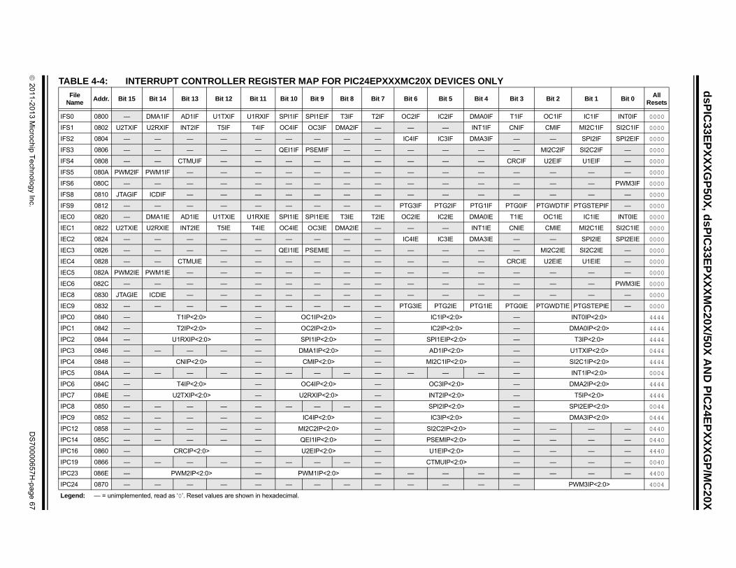
2
01
1-2
01
3 M
icroch
ip T
ech
no
log
y Inc.
DS
70
00
06
57
H-p
ag
e 6
7
ds
PIC
33E
PX
XX
GP
50X
, ds
PIC
33E
PX
XX
MC
20X
/50X
AN
D P
IC2
4EP
XX
XG
P/M
C2
0X
TA
N3 Bit 2 Bit 1 Bit 0
AllResets
IFS F OC1IF IC1IF INT0IF 0000
IFS F CMIF MI2C1IF SI2C1IF 0000
IFS — SPI2IF SPI2EIF 0000
IFS MI2C2IF SI2C2IF — 0000
IFS IF U2EIF U1EIF — 0000
IFS — — — 0000
IFS — — PWM3IF 0000
IFS — — — 0000
IFS IF PTGWDTIF PTGSTEPIF — 0000
IEC E OC1IE IC1IE INT0IE 0000
IEC E CMIE MI2C1IE SI2C1IE 0000
IEC — SPI2IE SPI2EIE 0000
IEC MI2C2IE SI2C2IE — 0000
IEC IE U2EIE U1EIE — 0000
IEC — — — 0000
IEC — — PWM3IE 0000
IEC — — — 0000
IEC IE PTGWDTIE PTGSTEPIE — 0000
IPC INT0IP<2:0> 4444
IPC DMA0IP<2:0> 4444
IPC T3IP<2:0> 4444
IPC U1TXIP<2:0> 0444
IPC SI2C1IP<2:0> 4444
IPC INT1IP<2:0> 0004
IPC DMA2IP<2:0> 4444
IPC T5IP<2:0> 4444
IPC SPI2EIP<2:0> 0044
IPC DMA3IP<2:0> 0444
IPC — — — 0440
IPC — — — 0440
IPC — — — 4440
IPC — — — 0040
IPC — — — 4400
IPC PWM3IP<2:0> 4004
Le
BLE 4-4: INTERRUPT CONTROLLER REGISTER MAP FOR PIC24EPXXXMC20X DEVICES ONLY
File ame
Addr. Bit 15 Bit 14 Bit 13 Bit 12 Bit 11 Bit 10 Bit 9 Bit 8 Bit 7 Bit 6 Bit 5 Bit 4 Bit
0 0800 — DMA1IF AD1IF U1TXIF U1RXIF SPI1IF SPI1EIF T3IF T2IF OC2IF IC2IF DMA0IF T1I
1 0802 U2TXIF U2RXIF INT2IF T5IF T4IF OC4IF OC3IF DMA2IF — — — INT1IF CNI
2 0804 — — — — — — — — — IC4IF IC3IF DMA3IF —
3 0806 — — — — — QEI1IF PSEMIF — — — — — —
4 0808 — — CTMUIF — — — — — — — — — CRC
5 080A PWM2IF PWM1IF — — — — — — — — — — —
6 080C — — — — — — — — — — — — —
8 0810 JTAGIF ICDIF — — — — — — — — — — —
9 0812 — — — — — — — — — PTG3IF PTG2IF PTG1IF PTG0
0 0820 — DMA1IE AD1IE U1TXIE U1RXIE SPI1IE SPI1EIE T3IE T2IE OC2IE IC2IE DMA0IE T1I
1 0822 U2TXIE U2RXIE INT2IE T5IE T4IE OC4IE OC3IE DMA2IE — — — INT1IE CNI
2 0824 — — — — — — — — — IC4IE IC3IE DMA3IE —
3 0826 — — — — — QEI1IE PSEMIE — — — — — —
4 0828 — — CTMUIE — — — — — — — — — CRC
5 082A PWM2IE PWM1IE — — — — — — — — — — —
6 082C — — — — — — — — — — — — —
8 0830 JTAGIE ICDIE — — — — — — — — — — —
9 0832 — — — — — — — — — PTG3IE PTG2IE PTG1IE PTG0
0 0840 — T1IP<2:0> — OC1IP<2:0> — IC1IP<2:0> —
1 0842 — T2IP<2:0> — OC2IP<2:0> — IC2IP<2:0> —
2 0844 — U1RXIP<2:0> — SPI1IP<2:0> — SPI1EIP<2:0> —
3 0846 — — — — — DMA1IP<2:0> — AD1IP<2:0> —
4 0848 — CNIP<2:0> — CMIP<2:0> — MI2C1IP<2:0> —
5 084A — — — — — — — — — — — — —
6 084C — T4IP<2:0> — OC4IP<2:0> — OC3IP<2:0> —
7 084E — U2TXIP<2:0> — U2RXIP<2:0> — INT2IP<2:0> —
8 0850 — — — — — — — — — SPI2IP<2:0> —
9 0852 — — — — — IC4IP<2:0> — IC3IP<2:0> —
12 0858 — — — — — MI2C2IP<2:0> — SI2C2IP<2:0> —
14 085C — — — — — QEI1IP<2:0> — PSEMIP<2:0> —
16 0860 — CRCIP<2:0> — U2EIP<2:0> — U1EIP<2:0> —
19 0866 — — — — — — — — — CTMUIP<2:0> —
23 086E — PWM2IP<2:0> — PWM1IP<2:0> — — — — —
24 0870 — — — — — — — — — — — — —
gend: — = unimplemented, read as ‘0’. Reset values are shown in hexadecimal.
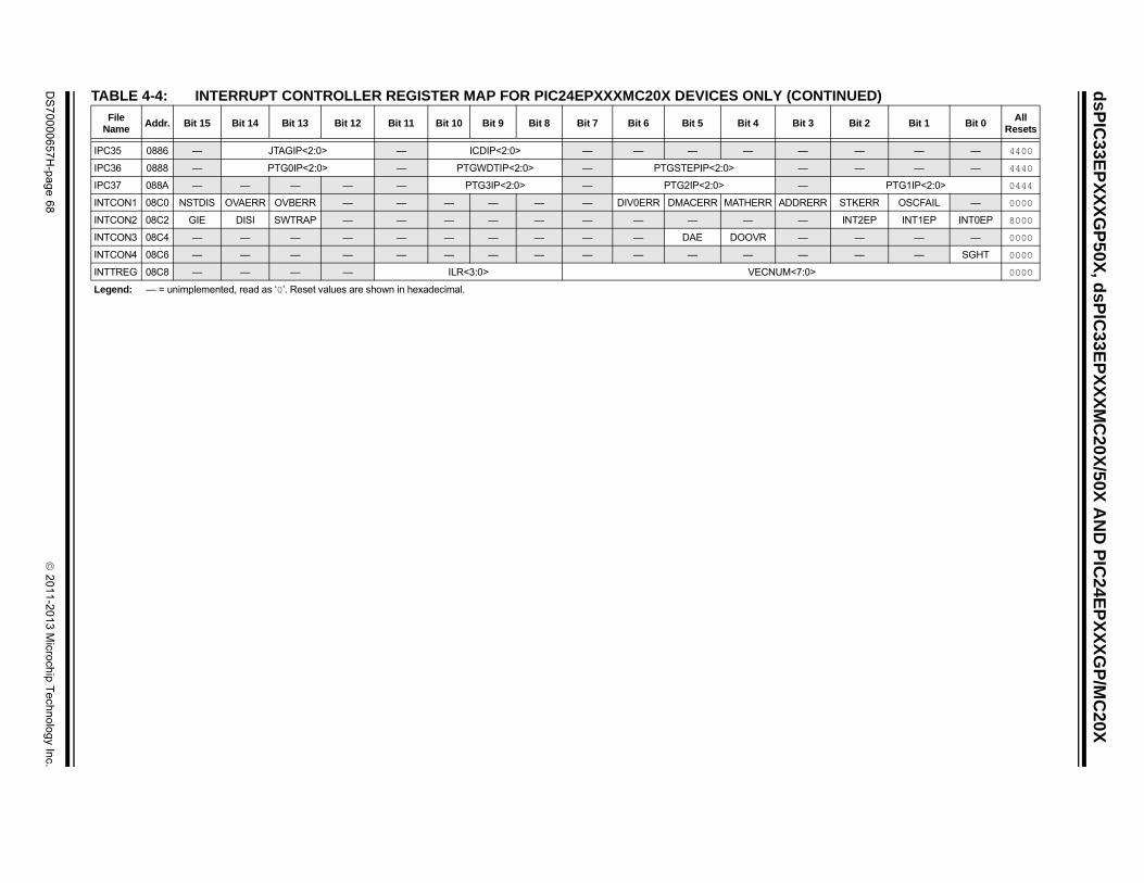
ds
PIC
33E
PX
XX
GP
50X
, dsP
IC33
EP
XX
XM
C20
X/5
0X A
ND
PIC
24E
PX
XX
GP
/MC
20X
DS
70
00
06
57
H-p
ag
e 6
8
20
11
-20
13
Micro
chip
Te
chn
olo
gy In
c.
— — — — 4400
— — — — 4440
— PTG1IP<2:0> 0444
DDRERR STKERR OSCFAIL — 0000
— INT2EP INT1EP INT0EP 8000
— — — — 0000
— — — SGHT 0000
M<7:0> 0000
(CONTINUED)
Bit 3 Bit 2 Bit 1 Bit 0All
Resets
IPC35 0886 — JTAGIP<2:0> — ICDIP<2:0> — — — —
IPC36 0888 — PTG0IP<2:0> — PTGWDTIP<2:0> — PTGSTEPIP<2:0>
IPC37 088A — — — — — PTG3IP<2:0> — PTG2IP<2:0>
INTCON1 08C0 NSTDIS OVAERR OVBERR — — — — — — DIV0ERR DMACERR MATHERR A
INTCON2 08C2 GIE DISI SWTRAP — — — — — — — — —
INTCON3 08C4 — — — — — — — — — — DAE DOOVR
INTCON4 08C6 — — — — — — — — — — — —
INTTREG 08C8 — — — — ILR<3:0> VECNU
TABLE 4-4: INTERRUPT CONTROLLER REGISTER MAP FOR PIC24EPXXXMC20X DEVICES ONLY
File Name
Addr. Bit 15 Bit 14 Bit 13 Bit 12 Bit 11 Bit 10 Bit 9 Bit 8 Bit 7 Bit 6 Bit 5 Bit 4
Legend: — = unimplemented, read as ‘0’. Reset values are shown in hexadecimal.

2
01
1-2
01
3 M
icroch
ip T
ech
no
log
y Inc.
DS
70
00
06
57
H-p
ag
e 6
9
ds
PIC
33E
PX
XX
GP
50X
, ds
PIC
33E
PX
XX
MC
20X
/50X
AN
D P
IC2
4EP
XX
XG
P/M
C2
0X
TA
Nit 3 Bit 2 Bit 1 Bit 0
AllResets
IFS 1IF OC1IF IC1IF INT0IF 0000
IFS NIF CMIF MI2C1IF SI2C1IF 0000
IFS 1IF C1RXIF SPI2IF SPI2EIF 0000
IFS — MI2C2IF SI2C2IF — 0000
IFS CIF U2EIF U1EIF — 0000
IFS — — — PWM3IF 0000
IFS — — — — 0000
IFS G0IF PTGWDTIF PTGSTEPIF — 0000
IEC 1IE OC1IE IC1IE INT0IE 0000
IEC NIE CMIE MI2C1IE SI2C1IE 0000
IEC 1IE C1RXIE SPI2IE SPI2EIE 0000
IEC — MI2C2IE SI2C2IE — 0000
IEC CIE U2EIE U1EIE — 0000
IEC — — — — 0000
IEC G0IE PTGWDTIE PTGSTEPIE — 0000
IPC — INT0IP<2:0> 4444
IPC — DMA0IP<2:0> 4444
IPC — T3IP<2:0> 4444
IPC — U1TXIP<2:0> 0444
IPC — SI2C1IP<2:0> 4444
IPC — INT1IP<2:0> 0004
IPC — DMA2IP<2:0> 4444
IPC — T5IP<2:0> 4444
IPC — SPI2EIP<2:0> 4444
IPC — DMA3IP<2:0> 0444
IPC — — — — 0000
IPC — — — — 0440
IPC — — — — 4440
IPC — — — — 0400
IPC — — — — 0040
IPC — — — — 4400
IPC — — — — 4440
IPC — PTG1IP<2:0> 0444
Le
BLE 4-5: INTERRUPT CONTROLLER REGISTER MAP FOR dsPIC33EPXXXGP50X DEVICES ONLY
File ame
Addr. Bit 15 Bit 14 Bit 13 Bit 12 Bit 11 Bit 10 Bit 9 Bit 8 Bit 7 Bit 6 Bit 5 Bit 4 B
0 0800 — DMA1IF AD1IF U1TXIF U1RXIF SPI1IF SPI1EIF T3IF T2IF OC2IF IC2IF DMA0IF T
1 0802 U2TXIF U2RXIF INT2IF T5IF T4IF OC4IF OC3IF DMA2IF — — — INT1IF C
2 0804 — — — — — — — — — IC4IF IC3IF DMA3IF C
3 0806 — — — — — — — — — — — —
4 0808 — — CTMUIF — — — — — — C1TXIF — — CR
6 080C — — — — — — — — — — — —
8 0810 JTAGIF ICDIF — — — — — — — — — —
9 0812 — — — — — — — — — PTG3IF PTG2IF PTG1IF PT
0 0820 — DMA1IE AD1IE U1TXIE U1RXIE SPI1IE SPI1EIE T3IE T2IE OC2IE IC2IE DMA0IE T
1 0822 U2TXIE U2RXIE INT2IE T5IE T4IE OC4IE OC3IE DMA2IE — — — INT1IE C
2 0824 — — — — — — — — — IC4IE IC3IE DMA3IE C
3 0826 — — — — — — — — — — — —
4 0828 — — CTMUIE — — — — — — C1TXIE — — CR
8 0830 JTAGIE ICDIE — — — — — — — — — —
9 0832 — — — — — — — — — PTG3IE PTG2IE PTG1IE PT
0 0840 — T1IP<2:0> — OC1IP<2:0> — IC1IP<2:0>
1 0842 — T2IP<2:0> — OC2IP<2:0> — IC2IP<2:0>
2 0844 — U1RXIP<2:0> — SPI1IP<2:0> — SPI1EIP<2:0>
3 0846 — — — — — DMA1IP<2:0> — AD1IP<2:0>
4 0848 — CNIP<2:0> — CMIP<2:0> — MI2C1IP<2:0>
5 084A — — — — — — — — — — — —
6 084C — T4IP<2:0> — OC4IP<2:0> — OC3IP<2:0>
7 084E — U2TXIP<2:0> — U2RXIP<2:0> — INT2IP<2:0>
8 0850 — C1IP<2:0> — C1RXIP<2:0> — SPI2IP<2:0>
9 0852 — — — — — IC4IP<2:0> — IC3IP<2:0>
11 0856 — — — — — — — — — — — —
12 0858 — — — — — MI2C2IP<2:0> — SI2C2IP<2:0>
16 0860 — CRCIP<2:0> — U2EIP<2:0> — U1EIP<2:0>
17 0862 — — — — — C1TXIP<2:0> — — — —
19 0866 — — — — — — — — — CTMUIP<2:0>
35 0886 — JTAGIP<2:0> — ICDIP<2:0> — — — —
36 0888 — PTG0IP<2:0> — PTGWDTIP<2:0> — PTGSTEPIP<2:0>
37 088A — — — — — PTG3IP<2:0> — PTG2IP<2:0>
gend: — = unimplemented, read as ‘0’. Reset values are shown in hexadecimal.
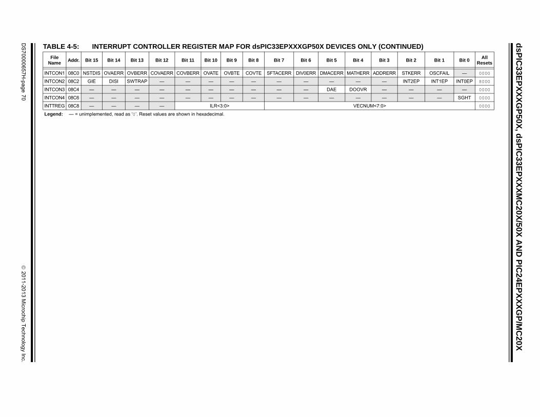
ds
PIC
33E
PX
XX
GP
50X
, dsP
IC33
EP
XX
XM
C20
X/5
0X A
ND
PIC
24E
PX
XX
GP
/MC
20X
DS
70
00
06
57
H-p
ag
e 7
0
20
11
-20
13
Micro
chip
Te
chn
olo
gy In
c.
ADDRERR STKERR OSCFAIL — 0000
— INT2EP INT1EP INT0EP 8000
— — — — 0000
— — — SGHT 0000
M<7:0> 0000
Y (CONTINUED)
Bit 3 Bit 2 Bit 1 Bit 0All
Resets
INTCON1 08C0 NSTDIS OVAERR OVBERR COVAERR COVBERR OVATE OVBTE COVTE SFTACERR DIV0ERR DMACERR MATHERR
INTCON2 08C2 GIE DISI SWTRAP — — — — — — — — —
INTCON3 08C4 — — — — — — — — — — DAE DOOVR
INTCON4 08C6 — — — — — — — — — — — —
INTTREG 08C8 — — — — ILR<3:0> VECNU
TABLE 4-5: INTERRUPT CONTROLLER REGISTER MAP FOR dsPIC33EPXXXGP50X DEVICES ONL
File Name
Addr. Bit 15 Bit 14 Bit 13 Bit 12 Bit 11 Bit 10 Bit 9 Bit 8 Bit 7 Bit 6 Bit 5 Bit 4
Legend: — = unimplemented, read as ‘0’. Reset values are shown in hexadecimal.

2
01
1-2
01
3 M
icroch
ip T
ech
no
log
y Inc.
DS
70
00
06
57
H-p
ag
e 7
1
ds
PIC
33E
PX
XX
GP
50X
, ds
PIC
33E
PX
XX
MC
20X
/50X
AN
D P
IC2
4EP
XX
XG
P/M
C2
0X
TA
NBit 3 Bit 2 Bit 1 Bit 0
AllResets
IFS T1IF OC1IF IC1IF INT0IF 0000
IFS NIF CMIF MI2C1IF SI2C1IF 0000
IFS — — SPI2IF SPI2EIF 0000
IFS — MI2C2IF SI2C2IF — 0000
IFS RCIF U2EIF U1EIF — 0000
IFS — — — — 0000
IFS — — — PWM3IF 0000
IFS — — — — 0000
IFS TG0IF PTGWDTIF PTGSTEPIF — 0000
IEC T1IE OC1IE IC1IE INT0IE 0000
IEC NIE CMIE MI2C1IE SI2C1IE 0000
IEC — — SPI2IE SPI2EIE 0000
IEC — MI2C2IE SI2C2IE — 0000
IEC RCIE U2EIE U1EIE — 0000
IEC — — — — 0000
IEC — — — PWM3IE 0000
IEC — — — — 0000
IEC G0IE PTGWDTIE PTGSTEPIE — 0000
IPC — INT0IP<2:0> 4444
IPC — DMA0IP<2:0> 4444
IPC — T3IP<2:0> 4444
IPC — U1TXIP<2:0> 0444
IPC — SI2C1IP<2:0> 4444
IPC — INT1IP<2:0> 0004
IPC — DMA2IP<2:0> 4444
IPC — T5IP<2:0> 4444
IPC — SPI2EIP<2:0> 0444
IPC — DMA3IP<2:0> 0444
IPC — — — — 0440
IPC — — — — 0440
IPC — — — — 4440
IPC — — — — 0040
IPC — — — — 4400
IPC — PWM3IP<2:0> 0004
Le
BLE 4-6: INTERRUPT CONTROLLER REGISTER MAP FOR dsPIC33EPXXXMC20X DEVICES ONLY
File ame
Addr. Bit 15 Bit 14 Bit 13 Bit 12 Bit 11 Bit 10 Bit 9 Bit 8 Bit 7 Bit 6 Bit 5 Bit 4
0 0800 — DMA1IF AD1IF U1TXIF U1RXIF SPI1IF SPI1EIF T3IF T2IF OC2IF IC2IF DMA0IF
1 0802 U2TXIF U2RXIF INT2IF T5IF T4IF OC4IF OC3IF DMA2IF — — — INT1IF C
2 0804 — — — — — — — — — IC4IF IC3IF DMA3IF
3 0806 — — — — — QEI1IF PSEMIF — — — — —
4 0808 — — CTMUIF — — — — — — — — — C
5 080A PWM2IF PWM1IF — — — — — — — — — —
6 080C — — — — — — — — — — — —
8 0810 JTAGIF ICDIF — — — — — — — — — —
9 0812 — — — — — — — — — PTG3IF PTG2IF PTG1IF P
0 0820 — DMA1IE AD1IE U1TXIE U1RXIE SPI1IE SPI1EIE T3IE T2IE OC2IE IC2IE DMA0IE
1 0822 U2TXIE U2RXIE INT2IE T5IE T4IE OC4IE OC3IE DMA2IE — — — INT1IE C
2 0824 — — — — — — — — — IC4IE IC3IE DMA3IE
3 0826 — — — — — QEI1IE PSEMIE — — — — —
4 0828 — — CTMUIE — — — — — — — — — C
5 082A PWM2IE PWM1IE — — — — — — — — — —
6 082C — — — — — — — — — — — —
8 0830 JTAGIE ICDIE — — — — — — — — — —
9 0832 — — — — — — — — — PTG3IE PTG2IE PTG1IE PT
0 0840 — T1IP<2:0> — OC1IP<2:0> — IC1IP<2:0>
1 0842 — T2IP<2:0> — OC2IP<2:0> — IC2IP<2:0>
2 0844 — U1RXIP<2:0> — SPI1IP<2:0> — SPI1EIP<2:0>
3 0846 — — — — — DMA1IP<2:0> — AD1IP<2:0>
4 0848 — CNIP<2:0> — CMIP<2:0> — MI2C1IP<2:0>
5 084A — — — — — — — — — — — —
6 084C — T4IP<2:0> — OC4IP<2:0> — OC3IP<2:0>
7 084E — U2TXIP<2:0> — U2RXIP<2:0> — INT2IP<2:0>
8 0850 — — — — — C1RXIP<2:0> — SPI2IP<2:0>
9 0852 — — — — — IC4IP<2:0> — IC3IP<2:0>
12 0858 — — — — — MI2C2IP<2:0> — SI2C2IP<2:0>
14 085C — — — — — QEI1IP<2:0> — PSEMIP<2:0>
16 0860 — CRCIP<2:0> — U2EIP<2:0> — U1EIP<2:0>
19 0866 — — — — — — — — — CTMUIP<2:0>
23 086E — PWM2IP<2:0> — PWM1IP<2:0> — — — —
24 0870 — — — — — — — — — — — —
gend: — = unimplemented, read as ‘0’. Reset values are shown in hexadecimal.

ds
PIC
33E
PX
XX
GP
50X
, dsP
IC33
EP
XX
XM
C20
X/5
0X A
ND
PIC
24E
PX
XX
GP
/MC
20X
DS
70
00
06
57
H-p
ag
e 7
2
20
11
-20
13
Micro
chip
Te
chn
olo
gy In
c.
— — — — 4400
— — — — 4440
— PTG1IP<2:0> 0444
ADDRERR STKERR OSCFAIL — 0000
— INT2EP INT1EP INT0EP 8000
— — — — 0000
— — — SGHT 0000
M<7:0> 0000
LY (CONTINUED)
Bit 3 Bit 2 Bit 1 Bit 0All
Resets
IPC35 0886 — JTAGIP<2:0> — ICDIP<2:0> — — — —
IPC36 0888 — PTG0IP<2:0> — PTGWDTIP<2:0> — PTGSTEPIP<2:0>
IPC37 088A — — — — — PTG3IP<2:0> — PTG2IP<2:0>
INTCON1 08C0 NSTDIS OVAERR OVBERR COVAERR COVBERR OVATE OVBTE COVTE SFTACERR DIV0ERR DMACERR MATHERR
INTCON2 08C2 GIE DISI SWTRAP — — — — — — — — —
INTCON3 08C4 — — — — — — — — — — DAE DOOVR
INTCON4 08C6 — — — — — — — — — — — —
INTTREG 08C8 — — — — ILR<3:0> VECNU
TABLE 4-6: INTERRUPT CONTROLLER REGISTER MAP FOR dsPIC33EPXXXMC20X DEVICES ON
File Name
Addr. Bit 15 Bit 14 Bit 13 Bit 12 Bit 11 Bit 10 Bit 9 Bit 8 Bit 7 Bit 6 Bit 5 Bit 4
Legend: — = unimplemented, read as ‘0’. Reset values are shown in hexadecimal.

2
01
1-2
01
3 M
icroch
ip T
ech
no
log
y Inc.
DS
70
00
06
57
H-p
ag
e 7
3
ds
PIC
33E
PX
XX
GP
50X
, ds
PIC
33E
PX
XX
MC
20X
/50X
AN
D P
IC2
4EP
XX
XG
P/M
C2
0X
TA
Nt 3 Bit 2 Bit 1 Bit 0
AllResets
IFS IF OC1IF IC1IF INT0IF 0000
IFS IF CMIF MI2C1IF SI2C1IF 0000
IFS IF C1RXIF SPI2IF SPI2EIF 0000
IFS MI2C2IF SI2C2IF — 0000
IFS CIF U2EIF U1EIF — 0000
IFS — — — 0000
IFS — — PWM3IF 0000
IFS — — — 0000
IFS 0IF PTGWDTIF PTGSTEPIF — 0000
IEC IE OC1IE IC1IE INT0IE 0000
IEC IE CMIE MI2C1IE SI2C1IE 0000
IEC IE C1RXIE SPI2IE SPI2EIE 0000
IEC MI2C2IE SI2C2IE — 0000
IEC CIE U2EIE U1EIE — 0000
IEC — — — 0000
IEC — — PWM3IE 0000
IEC — — — 0000
IEC — — — 0000
IEC 0IE PTGWDTIE PTGSTEPIE — 0000
IPC INT0IP<2:0> 4444
IPC DMA0IP<2:0> 4444
IPC T3IP<2:0> 4444
IPC U1TXIP<2:0> 0444
IPC SI2C1IP<2:0> 4444
IPC INT1IP<2:0> 0004
IPC DMA2IP<2:0> 4444
IPC T5IP<2:0> 4444
IPC SPI2EIP<2:0> 4444
IPC DMA3IP<2:0> 0444
IPC — — — 0440
IPC — — — 0440
IPC — — — 4440
IPC — — — 0400
IPC — — — 0040
Le
BLE 4-7: INTERRUPT CONTROLLER REGISTER MAP FOR dsPIC33EPXXXMC50X DEVICES ONLY
File ame
Addr. Bit 15 Bit 14 Bit 13 Bit 12 Bit 11 Bit 10 Bit 9 Bit 8 Bit 7 Bit 6 Bit 5 Bit 4 Bi
0 0800 — DMA1IF AD1IF U1TXIF U1RXIF SPI1IF SPI1EIF T3IF T2IF OC2IF IC2IF DMA0IF T1
1 0802 U2TXIF U2RXIF INT2IF T5IF T4IF OC4IF OC3IF DMA2IF — — — INT1IF CN
2 0804 — — — — — — — — — IC4IF IC3IF DMA3IF C1
3 0806 — — — — — QEI1IF PSEMIF — — — — — —
4 0808 — — CTMUIF — — — — — — C1TXIF — — CR
5 080A PWM2IF PWM1IF — — — — — — — — — — —
6 080C — — — — — — — — — — — — —
8 0810 JTAGIF ICDIF — — — — — — — — — — —
9 0812 — — — — — — — — — PTG3IF PTG2IF PTG1IF PTG
0 0820 — DMA1IE AD1IE U1TXIE U1RXIE SPI1IE SPI1EIE T3IE T2IE OC2IE IC2IE DMA0IE T1
1 0822 U2TXIE U2RXIE INT2IE T5IE T4IE OC4IE OC3IE DMA2IE — — — INT1IE CN
2 0824 — — — — — — — — — IC4IE IC3IE DMA3IE C1
3 0826 — — — — — QEI1IE PSEMIE — — — — — —
4 0828 — — CTMUIE — — — — — — C1TXIE — — CR
5 082A PWM2IE PWM1IE — — — — — — — — — — —
6 082C — — — — — — — — — — — — —
7 082E — — — — — — — — — — — — —
8 0830 JTAGIE ICDIE — — — — — — — — — — —
9 0832 — — — — — — — — — PTG3IE PTG2IE PTG1IE PTG
0 0840 — T1IP<2:0> — OC1IP<2:0> — IC1IP<2:0> —
1 0842 — T2IP<2:0> — OC2IP<2:0> — IC2IP<2:0> —
2 0844 — U1RXIP<2:0> — SPI1IP<2:0> — SPI1EIP<2:0> —
3 0846 — — — — — DMA1IP<2:0> — AD1IP<2:0> —
4 0848 — CNIP<2:0> — CMIP<2:0> — MI2C1IP<2:0> —
5 084A — — — — — — — — — — — — —
6 084C — T4IP<2:0> — OC4IP<2:0> — OC3IP<2:0> —
7 084E — U2TXIP<2:0> — U2RXIP<2:0> — INT2IP<2:0> —
8 0850 — C1IP<2:0> — C1RXIP<2:0> — SPI2IP<2:0> —
9 0852 — — — — — IC4IP<2:0> — IC3IP<2:0> —
12 0858 — — — — — MI2C2IP<2:0> — SI2C2IP<2:0> —
14 085C — — — — — QEI1IP<2:0> — PSEMIP<2:0> —
16 0860 — CRCIP<2:0> — U2EIP<2:0> — U1EIP<2:0> —
17 0862 — — — — — C1TXIP<2:0> — — — — —
19 0866 — — — — — — — — — CTMUIP<2:0> —
gend: — = unimplemented, read as ‘0’. Reset values are shown in hexadecimal.
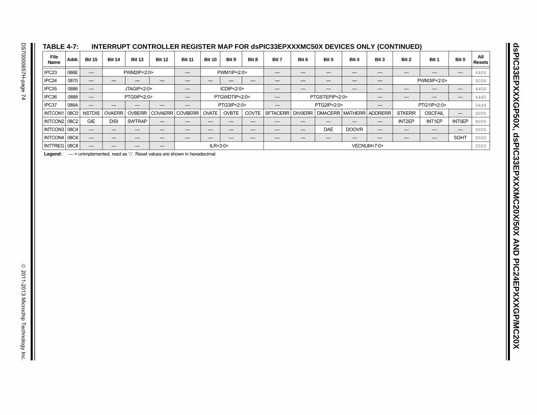
ds
PIC
33E
PX
XX
GP
50X
, dsP
IC33
EP
XX
XM
C20
X/5
0X A
ND
PIC
24E
PX
XX
GP
/MC
20X
DS
70
00
06
57
H-p
ag
e 7
4
20
11
-20
13
Micro
chip
Te
chn
olo
gy In
c.
— — — — 4400
— PWM3IP<2:0> 0004
— — — — 4400
— — — — 4440
— PTG1IP<2:0> 0444
ADDRERR STKERR OSCFAIL — 0000
— INT2EP INT1EP INT0EP 8000
— — — — 0000
— — — SGHT 0000
M<7:0> 0000
LY (CONTINUED)
Bit 3 Bit 2 Bit 1 Bit 0All
Resets
IPC23 086E — PWM2IP<2:0> — PWM1IP<2:0> — — — —
IPC24 0870 — — — — — — — — — — — —
IPC35 0886 — JTAGIP<2:0> — ICDIP<2:0> — — — —
IPC36 0888 — PTG0IP<2:0> — PTGWDTIP<2:0> — PTGSTEPIP<2:0>
IPC37 088A — — — — — PTG3IP<2:0> — PTG2IP<2:0>
INTCON1 08C0 NSTDIS OVAERR OVBERR COVAERR COVBERR OVATE OVBTE COVTE SFTACERR DIV0ERR DMACERR MATHERR
INTCON2 08C2 GIE DISI SWTRAP — — — — — — — — —
INTCON3 08C4 — — — — — — — — — — DAE DOOVR
INTCON4 08C6 — — — — — — — — — — — —
INTTREG 08C8 — — — — ILR<3:0> VECNU
TABLE 4-7: INTERRUPT CONTROLLER REGISTER MAP FOR dsPIC33EPXXXMC50X DEVICES ON
File Name
Addr. Bit 15 Bit 14 Bit 13 Bit 12 Bit 11 Bit 10 Bit 9 Bit 8 Bit 7 Bit 6 Bit 5 Bit 4
Legend: — = unimplemented, read as ‘0’. Reset values are shown in hexadecimal.

2
01
1-2
01
3 M
icroch
ip T
ech
no
log
y Inc.
DS
70
00
06
57
H-p
ag
e 7
5
ds
PIC
33E
PX
XX
GP
50X
, ds
PIC
33E
PX
XX
MC
20X
/50X
AN
D P
IC2
4EP
XX
XG
P/M
C2
0X
TA
Bit 3 Bit 2 Bit 1 Bit 0All
Resets
TM xxxx
PR FFFF
T1 — TSYNC TCS — 0000
TM xxxx
TM xxxx
TM xxxx
PR FFFF
PR FFFF
T2 T32 — TCS — 0000
T3 — — TCS — 0000
TM xxxx
TM xxxx
TM xxxx
PR FFFF
PR FFFF
T4 T32 — TCS — 0000
T5 — — TCS — 0000
Le
BLE 4-8: TIMER1 THROUGH TIMER5 REGISTER MAP
SFR Name
Addr. Bit 15 Bit 14 Bit 13 Bit 12 Bit 11 Bit 10 Bit 9 Bit 8 Bit 7 Bit 6 Bit 5 Bit 4
R1 0100 Timer1 Register
1 0102 Period Register 1
CON 0104 TON — TSIDL — — — — — — TGATE TCKPS<1:0>
R2 0106 Timer2 Register
R3HLD 0108 Timer3 Holding Register (for 32-bit timer operations only)
R3 010A Timer3 Register
2 010C Period Register 2
3 010E Period Register 3
CON 0110 TON — TSIDL — — — — — — TGATE TCKPS<1:0>
CON 0112 TON — TSIDL — — — — — — TGATE TCKPS<1:0>
R4 0114 Timer4 Register
R5HLD 0116 Timer5 Holding Register (for 32-bit operations only)
R5 0118 Timer5 Register
4 011A Period Register 4
5 011C Period Register 5
CON 011E TON — TSIDL — — — — — — TGATE TCKPS<1:0>
CON 0120 TON — TSIDL — — — — — — TGATE TCKPS<1:0>
gend: x = unknown value on Reset, — = unimplemented, read as ‘0’. Reset values are shown in hexadecimal.

ds
PIC
33E
PX
XX
GP
50X
, dsP
IC33
EP
XX
XM
C20
X/5
0X A
ND
PIC
24E
PX
XX
GP
/MC
20X
DS
70
00
06
57
H-p
ag
e 7
6
20
11
-20
13
Micro
chip
Te
chn
olo
gy In
c.
4 Bit 3 Bit 2 Bit 1 Bit 0All
Resets
V ICBNE ICM<2:0> 0000
SYNCSEL<4:0> 000D
xxxx
0000
V ICBNE ICM<2:0> 0000
SYNCSEL<4:0> 000D
xxxx
0000
V ICBNE ICM<2:0> 0000
SYNCSEL<4:0> 000D
xxxx
0000
V ICBNE ICM<2:0> 0000
SYNCSEL<4:0> 000D
xxxx
0000
TABLE 4-9: INPUT CAPTURE 1 THROUGH INPUT CAPTURE 4 REGISTER MAP
File Name Addr. Bit 15 Bit 14 Bit 13 Bit 12 Bit 11 Bit 10 Bit 9 Bit 8 Bit 7 Bit 6 Bit 5 Bit
IC1CON1 0140 — — ICSIDL ICTSEL<2:0> — — — ICI<1:0> ICO
IC1CON2 0142 — — — — — — — IC32 ICTRIG TRIGSTAT —
IC1BUF 0144 Input Capture 1 Buffer Register
IC1TMR 0146 Input Capture 1 Timer
IC2CON1 0148 — — ICSIDL ICTSEL<2:0> — — — ICI<1:0> ICO
IC2CON2 014A — — — — — — — IC32 ICTRIG TRIGSTAT —
IC2BUF 014C Input Capture 2 Buffer Register
IC2TMR 014E Input Capture 2 Timer
IC3CON1 0150 — — ICSIDL ICTSEL<2:0> — — — ICI<1:0> ICO
IC3CON2 0152 — — — — — — — IC32 ICTRIG TRIGSTAT —
IC3BUF 0154 Input Capture 3 Buffer Register
IC3TMR 0156 Input Capture 3 Timer
IC4CON1 0158 — — ICSIDL ICTSEL<2:0> — — — ICI<1:0> ICO
IC4CON2 015A — — — — — — — IC32 ICTRIG TRIGSTAT —
IC4BUF 015C Input Capture 4 Buffer Register
IC4TMR 015E Input Capture 4 Timer
Legend: x = unknown value on Reset, — = unimplemented, read as ‘0’. Reset values are shown in hexadecimal.

2
01
1-2
01
3 M
icroch
ip T
ech
no
log
y Inc.
DS
70
00
06
57
H-p
ag
e 7
7
ds
PIC
33E
PX
XX
GP
50X
, ds
PIC
33E
PX
XX
MC
20X
/50X
AN
D P
IC2
4EP
XX
XG
P/M
C2
0X
TA
Fi it 3 Bit 2 Bit 1 Bit 0All
Resets
OC MODE OCM<2:0> 0000
OC SYNCSEL<4:0> 000C
OC xxxx
OC xxxx
OC xxxx
OC MODE OCM<2:0> 0000
OC SYNCSEL<4:0> 000C
OC xxxx
OC xxxx
OC xxxx
OC MODE OCM<2:0> 0000
OC SYNCSEL<4:0> 000C
OC xxxx
OC xxxx
OC xxxx
OC MODE OCM<2:0> 0000
OC SYNCSEL<4:0> 000C
OC xxxx
OC xxxx
OC xxxx
Le
BLE 4-10: OUTPUT COMPARE 1 THROUGH OUTPUT COMPARE 4 REGISTER MAP
le Name Addr. Bit 15 Bit 14 Bit 13 Bit 12 Bit 11 Bit 10 Bit 9 Bit 8 Bit 7 Bit 6 Bit 5 Bit 4 B
1CON1 0900 — — OCSIDL OCTSEL<2:0> — ENFLTB ENFLTA — OCFLTB OCFLTA TRIG
1CON2 0902 FLTMD FLTOUT FLTTRIEN OCINV — — — OC32 OCTRIG TRIGSTAT OCTRIS
1RS 0904 Output Compare 1 Secondary Register
1R 0906 Output Compare 1 Register
1TMR 0908 Timer Value 1 Register
2CON1 090A — — OCSIDL OCTSEL<2:0> — ENFLTB ENFLTA — OCFLTB OCFLTA TRIG
2CON2 090C FLTMD FLTOUT FLTTRIEN OCINV — — — OC32 OCTRIG TRIGSTAT OCTRIS
2RS 090E Output Compare 2 Secondary Register
2R 0910 Output Compare 2 Register
2TMR 0912 Timer Value 2 Register
3CON1 0914 — — OCSIDL OCTSEL<2:0> — ENFLTB ENFLTA — OCFLTB OCFLTA TRIG
3CON2 0916 FLTMD FLTOUT FLTTRIEN OCINV — — — OC32 OCTRIG TRIGSTAT OCTRIS
3RS 0918 Output Compare 3 Secondary Register
3R 091A Output Compare 3 Register
3TMR 091C Timer Value 3 Register
4CON1 091E — — OCSIDL OCTSEL<2:0> — ENFLTB ENFLTA — OCFLTB OCFLTA TRIG
4CON2 0920 FLTMD FLTOUT FLTTRIEN OCINV — — — OC32 OCTRIG TRIGSTAT OCTRIS
4RS 0922 Output Compare 4 Secondary Register
4R 0924 Output Compare 4 Register
4TMR 0926 Timer Value 4 Register
gend: x = unknown value on Reset, — = unimplemented, read as ‘0’. Reset values are shown in hexadecimal.

ds
PIC
33E
PX
XX
GP
50X
, dsP
IC33
EP
XX
XM
C20
X/5
0X A
ND
PIC
24E
PX
XX
GP
/MC
20X
DS
70
00
06
57
H-p
ag
e 7
8
20
11
-20
13
Micro
chip
Te
chn
olo
gy In
c.
t 4 Bit 3 Bit 2 Bit 1 Bit 0All
Resets
— — PTGITM<1:0> 0000
— PTGWDT<2:0> 0000
1CS OC4TSS OC3TSS OC2TSS OC1TSS 0000
0000
0000
0000
0000
0000
0000
0000
0000
PTGQPTR<4:0> 0000
TEP0<7:0> 0000
TEP2<7:0> 0000
TEP4<7:0> 0000
TEP6<7:0> 0000
TEP8<7:0> 0000
EP10<7:0> 0000
EP12<7:0> 0000
EP14<7:0> 0000
TABLE 4-11: PTG REGISTER MAP
File Name Addr. Bit 15 Bit 14 Bit 13 Bit 12 Bit 11 Bit 10 Bit 9 Bit 8 Bit 7 Bit 6 Bit 5 Bi
PTGCST 0AC0 PTGEN — PTGSIDL PTGTOGL — PTGSWT PTGSSEN PTGIVIS PTGSTRT PTGWTO — —
PTGCON 0AC2 PTGCLK<2:0> PTGDIV<4:0> PTGPWD<3:0>
PTGBTE 0AC4 ADCTS<4:1> IC4TSS IC3TSS IC2TSS IC1TSS OC4CS OC3CS OC2CS OC
PTGHOLD 0AC6 PTGHOLD<15:0>
PTGT0LIM 0AC8 PTGT0LIM<15:0>
PTGT1LIM 0ACA PTGT1LIM<15:0>
PTGSDLIM 0ACC PTGSDLIM<15:0>
PTGC0LIM 0ACE PTGC0LIM<15:0>
PTGC1LIM 0AD0 PTGC1LIM<15:0>
PTGADJ 0AD2 PTGADJ<15:0>
PTGL0 0AD4 PTGL0<15:0>
PTGQPTR 0AD6 — — — — — — — — — — —
PTGQUE0 0AD8 STEP1<7:0> S
PTGQUE1 0ADA STEP3<7:0> S
PTGQUE2 0ADC STEP5<7:0> S
PTGQUE3 0ADE STEP7<7:0> S
PTGQUE4 0AE0 STEP9<7:0> S
PTGQUE5 0AE2 STEP11<7:0> ST
PTGQUE6 0AE4 STEP13<7:0> ST
PTGQUE7 0AE6 STEP15<7:0> ST
Legend: — = unimplemented, read as ‘0’. Reset values are shown in hexadecimal.

2
01
1-2
01
3 M
icroch
ip T
ech
no
log
y Inc.
DS
70
00
06
57
H-p
ag
e 7
9
ds
PIC
33E
PX
XX
GP
50X
, ds
PIC
33E
PX
XX
MC
20X
/50X
AN
D P
IC2
4EP
XX
XG
P/M
C2
0X
TA ONLY
F Bit 3 Bit 2 Bit 1 Bit 0All
Resets
PT SEVTPS<3:0> 0000
PT — PCLKDIV<2:0> 0000
PT 00F8
SE 0000
MD 0000
CH 0000
PW 0000
Le
TA C20X DEVICES ONLY
Fi Bit 3 Bit 2 Bit 1 Bit 0All
Resets
PW TBS CAM XPRES IUE 0000
IO CLDAT<1:0> SWAP OSYNC C000
FC FLTPOL FLTMOD<1:0> 0000
PD FFF8
PH 0000
DT 0000
AL 0000
TR 0000
TR TRGSTRT<5:0> 0000
LE PHH BPHL BPLH BPLL 0000
LE 0000
AU <3:0> CHOPHEN CHOPLEN 0000
Le
BLE 4-12: PWM REGISTER MAP FOR dsPIC33EPXXXMC20X/50X AND PIC24EPXXXMC20X DEVICES
ile Name Addr. Bit 15 Bit 14 Bit 13 Bit 12 Bit 11 Bit 10 Bit 9 Bit 8 Bit 7 Bit 6 Bit 5 Bit 4
CON 0C00 PTEN — PTSIDL SESTAT SEIEN EIPU SYNCPOL SYNCOEN SYNCEN SYNCSRC<2:0>
CON2 0C02 — — — — — — — — — — — —
PER 0C04 PTPER<15:0>
VTCMP 0C06 SEVTCMP<15:0>
C 0C0A MDC<15:0>
OP 0C1A CHPCLKEN — — — — — CHOPCLK<9:0>
MKEY 0C1E PWMKEY<15:0>
gend: — = unimplemented, read as ‘0’. Reset values are shown in hexadecimal.
BLE 4-13: PWM GENERATOR 1 REGISTER MAP FOR dsPIC33EPXXXMC20X/50X AND PIC24EPXXXM
le Name Addr. Bit 15 Bit 14 Bit 13 Bit 12 Bit 11 Bit 10 Bit 9 Bit 8 Bit 7 Bit 6 Bit 5 Bit 4
MCON1 0C20 FLTSTAT CLSTAT TRGSTAT FLTIEN CLIEN TRGIEN ITB MDCS DTC<1:0> DTCP — M
CON1 0C22 PENH PENL POLH POLL PMOD<1:0> OVRENH OVRENL OVRDAT<1:0> FLTDAT<1:0>
LCON1 0C24 — CLSRC<4:0> CLPOL CLMOD FLTSRC<4:0>
C1 0C26 PDC1<15:0>
ASE1 0C28 PHASE1<15:0>
R1 0C2A — — DTR1<13:0>
TDTR1 0C2C — — ALTDTR1<13:0>
IG1 0C32 TRGCMP<15:0>
GCON1 0C34 TRGDIV<3:0> — — — — — —
BCON1 0C3A PHR PHF PLR PLF FLTLEBEN CLLEBEN — — — — BCH BCL B
BDLY1 0C3C — — — — LEB<11:0>
XCON1 0C3E — — — — BLANKSEL<3:0> — — CHOPSEL
gend: — = unimplemented, read as ‘0’. Reset values are shown in hexadecimal.

ds
PIC
33E
PX
XX
GP
50X
, dsP
IC33
EP
XX
XM
C20
X/5
0X A
ND
PIC
24E
PX
XX
GP
/MC
20X
DS
70
00
06
57
H-p
ag
e 8
0
20
11
-20
13
Micro
chip
Te
chn
olo
gy In
c.
XXMC20X DEVICES ONLY
it 4 Bit 3 Bit 2 Bit 1 Bit 0All
Resets
MTBS CAM XPRES IUE 0000
:0> CLDAT<1:0> SWAP OSYNC C000
FLTPOL FLTMOD<1:0> 00F8
0000
0000
0000
0000
0000
TRGSTRT<5:0> 0000
CL BPHH BPHL BPLH BPLL 0000
0000
OPSEL<3:0> CHOPHEN CHOPLEN 0000
XXMC20X DEVICES ONLY
4 Bit 3 Bit 2 Bit 1 Bit 0All
Resets
MTBS CAM XPRES IUE 0000
> CLDAT<1:0> SWAP OSYNC C000
FLTPOL FLTMOD<1:0> 00F8
0000
0000
0000
0000
0000
TRGSTRT<5:0> 0000
L BPHH BPHL BPLH BPLL 0000
0000
PSEL<3:0> CHOPHEN CHOPLEN 0000
TABLE 4-14: PWM GENERATOR 2 REGISTER MAP FOR dsPIC33EPXXXMC20X/50X AND PIC24EPX
File Name Addr. Bit 15 Bit 14 Bit 13 Bit 12 Bit 11 Bit 10 Bit 9 Bit 8 Bit 7 Bit 6 Bit 5 B
PWMCON2 0C40 FLTSTAT CLSTAT TRGSTAT FLTIEN CLIEN TRGIEN ITB MDCS DTC<1:0> DTCP —
IOCON2 0C42 PENH PENL POLH POLL PMOD<1:0> OVRENH OVRENL OVRDAT<1:0> FLTDAT<1
FCLCON2 0C44 — CLSRC<4:0> CLPOL CLMOD FLTSRC<4:0>
PDC2 0C46 PDC2<15:0>
PHASE2 0C48 PHASE2<15:0>
DTR2 0C4A — — DTR2<13:0>
ALTDTR2 0C4C — — ALTDTR2<13:0>
TRIG2 0C52 TRGCMP<15:0>
TRGCON2 0C54 TRGDIV<3:0> — — — — — —
LEBCON2 0C5A PHR PHF PLR PLF FLTLEBEN CLLEBEN — — — — BCH B
LEBDLY2 0C5C — — — — LEB<11:0>
AUXCON2 0C5E — — — — BLANKSEL<3:0> — — CH
Legend: — = unimplemented, read as ‘0’. Reset values are shown in hexadecimal.
TABLE 4-15: PWM GENERATOR 3 REGISTER MAP FOR dsPIC33EPXXXMC20X/50X AND PIC24EPX
File Name Addr. Bit 15 Bit 14 Bit 13 Bit 12 Bit 11 Bit 10 Bit 9 Bit 8 Bit 7 Bit 6 Bit 5 Bit
PWMCON3 0C60 FLTSTAT CLSTAT TRGSTAT FLTIEN CLIEN TRGIEN ITB MDCS DTC<1:0> DTCP —
IOCON3 0C62 PENH PENL POLH POLL PMOD<1:0> OVRENH OVRENL OVRDAT<1:0> FLTDAT<1:0
FCLCON3 0C64 — CLSRC<4:0> CLPOL CLMOD FLTSRC<4:0>
PDC3 0C66 PDC3<15:0>
PHASE3 0C68 PHASE3<15:0>
DTR3 0C6A — — DTR3<13:0>
ALTDTR3 0C6C — — ALTDTR3<13:0>
TRIG3 0C72 TRGCMP<15:0>
TRGCON3 0C74 TRGDIV<3:0> — — — — — —
LEBCON3 0C7A PHR PHF PLR PLF FLTLEBEN CLLEBEN — — — — BCH BC
LEBDLY3 0C7C — — — — LEB<11:0>
AUXCON3 0C7E — — — — BLANKSEL<3:0> — — CHO
Legend: — = unimplemented, read as ‘0’. Reset values are shown in hexadecimal.
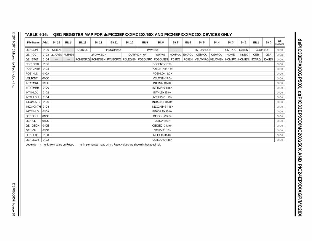
2
01
1-2
01
3 M
icroch
ip T
ech
no
log
y Inc.
DS
70
00
06
57
H-p
ag
e 8
1
ds
PIC
33E
PX
XX
GP
50X
, ds
PIC
33E
PX
XX
MC
20X
/50X
AN
D P
IC2
4EP
XX
XG
P/M
C2
0X
TA ONLY
Fil Bit 3 Bit 2 Bit 1 Bit 0All
Resets
QEI CNTPOL GATEN CCM<1:0> 0000
QEI L HOME INDEX QEB QEA 000x
QEI N HOMIRQ HOMIEN IDXIRQ IDXIEN 0000
POS 0000
POS 0000
POS 0000
VEL 0000
INT 0000
INT 0000
INT 0000
INT 0000
IND 0000
IND 0000
IND 0000
QEI 0000
QEI 0000
QEI 0000
QEI 0000
QEI 0000
QEI 0000
Leg
BLE 4-16: QEI1 REGISTER MAP FOR dsPIC33EPXXXMC20X/50X AND PIC24EPXXXMC20X DEVICES
e Name Addr. Bit 15 Bit 14 Bit 13 Bit 12 Bit 11 Bit 10 Bit 9 Bit 8 Bit 7 Bit 6 Bit 5 Bit 4
1CON 01C0 QEIEN — QEISIDL PIMOD<2:0> IMV<1:0> — INTDIV<2:0>
1IOC 01C2 QCAPEN FLTREN QFDIV<2:0> OUTFNC<1:0> SWPAB HOMPOL IDXPOL QEBPOL QEAPO
1STAT 01C4 — — PCHEQIRQ PCHEQIEN PCLEQIRQ PCLEQIEN POSOVIRQ POSOVIEN PCIIRQ PCIIEN VELOVIRQ VELOVIE
1CNTL 01C6 POSCNT<15:0>
1CNTH 01C8 POSCNT<31:16>
1HLD 01CA POSHLD<15:0>
1CNT 01CC VELCNT<15:0>
1TMRL 01CE INTTMR<15:0>
1TMRH 01D0 INTTMR<31:16>
1HLDL 01D2 INTHLD<15:0>
1HLDH 01D4 INTHLD<31:16>
X1CNTL 01D6 INDXCNT<15:0>
X1CNTH 01D8 INDXCNT<31:16>
X1HLD 01DA INDXHLD<15:0>
1GECL 01DC QEIGEC<15:0>
1ICL 01DC QEIIC<15:0>
1GECH 01DE QEIGEC<31:16>
1ICH 01DE QEIIC<31:16>
1LECL 01E0 QEILEC<15:0>
1LECH 01E2 QEILEC<31:16>
end: x = unknown value on Reset, — = unimplemented, read as ‘0’. Reset values are shown in hexadecimal.

ds
PIC
33E
PX
XX
GP
50X
, dsP
IC33
EP
XX
XM
C20
X/5
0X A
ND
PIC
24E
PX
XX
GP
/MC
20X
DS
70
00
06
57
H-p
ag
e 8
2
20
11
-20
13
Micro
chip
Te
chn
olo
gy In
c.
Bit 3 Bit 2 Bit 1 Bit 0All
Resets
ive Register 0000
mit Register 00FF
erator 0000
RCEN PEN RSEN SEN 1000
S R_W RBF TBF 0000
r 0000
0000
ive Register 0000
mit Register 00FF
erator 0000
RCEN PEN RSEN SEN 1000
S R_W RBF TBF 0000
r 0000
0000
Bit 3 Bit 2 Bit 1 Bit 0All
Resets
V BRGH PDSEL<1:0> STSEL 0000
E PERR FERR OERR URXDA 0110
it Register xxxx
e Register 0000
0000
V BRGH PDSEL<1:0> STSEL 0000
E PERR FERR OERR URXDA 0110
it Register xxxx
e Register 0000
0000
TABLE 4-17: I2C1 AND I2C2 REGISTER MAP
File Name
Addr. Bit 15 Bit 14 Bit 13 Bit 12 Bit 11 Bit 10 Bit 9 Bit 8 Bit 7 Bit 6 Bit 5 Bit 4
I2C1RCV 0200 — — — — — — — — I2C1 Rece
I2C1TRN 0202 — — — — — — — — I2C1 Trans
I2C1BRG 0204 — — — — — — — Baud Rate Gen
I2C1CON 0206 I2CEN — I2CSIDL SCLREL IPMIEN A10M DISSLW SMEN GCEN STREN ACKDT ACKEN
I2C1STAT 0208 ACKSTAT TRSTAT — — — BCL GCSTAT ADD10 IWCOL I2COV D_A P
I2C1ADD 020A — — — — — — I2C1 Address Registe
I2C1MSK 020C — — — — — — I2C1 Address Mask
I2C2RCV 0210 — — — — — — — — I2C2 Rece
I2C2TRN 0212 — — — — — — — — I2C2 Trans
I2C2BRG 0214 — — — — — — — Baud Rate Gen
I2C2CON 0216 I2CEN — I2CSIDL SCLREL IPMIEN A10M DISSLW SMEN GCEN STREN ACKDT ACKEN
I2C2STAT 0218 ACKSTAT TRSTAT — — — BCL GCSTAT ADD10 IWCOL I2COV D_A P
I2C2ADD 021A — — — — — — I2C2 Address Registe
I2C2MSK 021C — — — — — — I2C2 Address Mask
Legend: — = unimplemented, read as ‘0’. Reset values are shown in hexadecimal.
TABLE 4-18: UART1 AND UART2 REGISTER MAP
SFR Name
Addr. Bit 15 Bit 14 Bit 13 Bit 12 Bit 11 Bit 10 Bit 9 Bit 8 Bit 7 Bit 6 Bit 5 Bit 4
U1MODE 0220 UARTEN — USIDL IREN RTSMD — UEN<1:0> WAKE LPBACK ABAUD URXIN
U1STA 0222 UTXISEL1 UTXINV UTXISEL0 — UTXBRK UTXEN UTXBF TRMT URXISEL<1:0> ADDEN RIDL
U1TXREG 0224 — — — — — — — UART1 Transm
U1RXREG 0226 — — — — — — — UART1 Receiv
U1BRG 0228 Baud Rate Generator Prescaler
U2MODE 0230 UARTEN — USIDL IREN RTSMD — UEN<1:0> WAKE LPBACK ABAUD URXIN
U2STA 0232 UTXISEL1 UTXINV UTXISEL0 — UTXBRK UTXEN UTXBF TRMT URXISEL<1:0> ADDEN RIDL
U2TXREG 0234 — — — — — — — UART2 Transm
U2RXREG 0236 — — — — — — — UART2 Receiv
U2BRG 0238 Baud Rate Generator Prescaler
Legend: x = unknown value on Reset, — = unimplemented, read as ‘0’. Reset values are shown in hexadecimal.
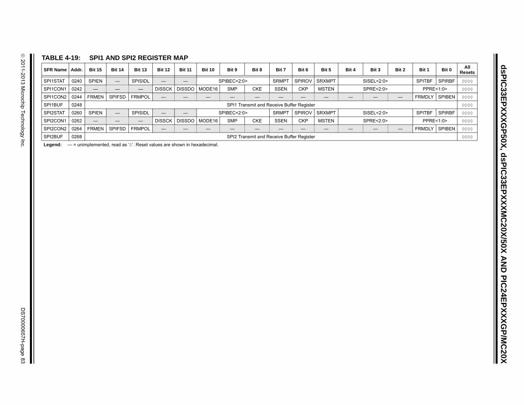
2
01
1-2
01
3 M
icroch
ip T
ech
no
log
y Inc.
DS
70
00
06
57
H-p
ag
e 8
3
ds
PIC
33E
PX
XX
GP
50X
, ds
PIC
33E
PX
XX
MC
20X
/50X
AN
D P
IC2
4EP
XX
XG
P/M
C2
0X
TA
SF Bit 3 Bit 2 Bit 1 Bit 0All
Resets
SP EL<2:0> SPITBF SPIRBF 0000
SP RE<2:0> PPRE<1:0> 0000
SP — — FRMDLY SPIBEN 0000
SP 0000
SP EL<2:0> SPITBF SPIRBF 0000
SP RE<2:0> PPRE<1:0> 0000
SP — — FRMDLY SPIBEN 0000
SP 0000
Le
BLE 4-19: SPI1 AND SPI2 REGISTER MAP
R Name Addr. Bit 15 Bit 14 Bit 13 Bit 12 Bit 11 Bit 10 Bit 9 Bit 8 Bit 7 Bit 6 Bit 5 Bit 4
I1STAT 0240 SPIEN — SPISIDL — — SPIBEC<2:0> SRMPT SPIROV SRXMPT SIS
I1CON1 0242 — — — DISSCK DISSDO MODE16 SMP CKE SSEN CKP MSTEN SP
I1CON2 0244 FRMEN SPIFSD FRMPOL — — — — — — — — —
I1BUF 0248 SPI1 Transmit and Receive Buffer Register
I2STAT 0260 SPIEN — SPISIDL — — SPIBEC<2:0> SRMPT SPIROV SRXMPT SIS
I2CON1 0262 — — — DISSCK DISSDO MODE16 SMP CKE SSEN CKP MSTEN SP
I2CON2 0264 FRMEN SPIFSD FRMPOL — — — — — — — — —
I2BUF 0268 SPI2 Transmit and Receive Buffer Register
gend: — = unimplemented, read as ‘0’. Reset values are shown in hexadecimal.

ds
PIC
33E
PX
XX
GP
50X
, dsP
IC33
EP
XX
XM
C20
X/5
0X A
ND
PIC
24E
PX
XX
GP
/MC
20X
DS
70
00
06
57
H-p
ag
e 8
4
20
11
-20
13
Micro
chip
Te
chn
olo
gy In
c.
t 4 Bit 3 Bit 2 Bit 1 Bit 0All
Resets
xxxx
xxxx
xxxx
xxxx
xxxx
xxxx
xxxx
xxxx
xxxx
xxxx
xxxx
xxxx
xxxx
xxxx
xxxx
xxxx
CG SIMSAM ASAM SAMP DONE 0000
<4:0> BUFM ALTS 0000
DCS<7:0> 0000
— CH123NA<1:0> CH123SA 0000
CH0SA<4:0> 0000
— — — — 0000
S4 CSS3 CSS2 CSS1 CSS0 0000
— DMABL<2:0> 0000
TABLE 4-20: ADC1 REGISTER MAP
File Name Addr. Bit 15 Bit 14 Bit 13 Bit 12 Bit 11 Bit 10 Bit 9 Bit 8 Bit 7 Bit 6 Bit 5 Bi
ADC1BUF0 0300 ADC1 Data Buffer 0
ADC1BUF1 0302 ADC1 Data Buffer 1
ADC1BUF2 0304 ADC1 Data Buffer 2
ADC1BUF3 0306 ADC1 Data Buffer 3
ADC1BUF4 0308 ADC1 Data Buffer 4
ADC1BUF5 030A ADC1 Data Buffer 5
ADC1BUF6 030C ADC1 Data Buffer 6
ADC1BUF7 030E ADC1 Data Buffer 7
ADC1BUF8 0310 ADC1 Data Buffer 8
ADC1BUF9 0312 ADC1 Data Buffer 9
ADC1BUFA 0314 ADC1 Data Buffer 10
ADC1BUFB 0316 ADC1 Data Buffer 11
ADC1BUFC 0318 ADC1 Data Buffer 12
ADC1BUFD 031A ADC1 Data Buffer 13
ADC1BUFE 031C ADC1 Data Buffer 14
ADC1BUFF 031E ADC1 Data Buffer 15
AD1CON1 0320 ADON — ADSIDL ADDMABM — AD12B FORM<1:0> SSRC<2:0> SSR
AD1CON2 0322 VCFG<2:0> — — CSCNA CHPS<1:0> BUFS SMPI
AD1CON3 0324 ADRC — — SAMC<4:0> A
AD1CHS123 0326 — — — — — CH123NB<1:0> CH123SB — — — —
AD1CHS0 0328 CH0NB — — CH0SB<4:0> CH0NA — —
AD1CSSH 032E CSS31 CSS30 — — — CSS26 CSS25 CSS24 — — — —
AD1CSSL 0330 CSS15 CSS14 CSS13 CSS12 CSS11 CSS10 CSS9 CSS8 CSS7 CSS6 CSS5 CS
AD1CON4 0332 — — — — — — — ADDMAEN — — — —
Legend: x = unknown value on Reset, — = unimplemented, read as ‘0’. Reset values are shown in hexadecimal.
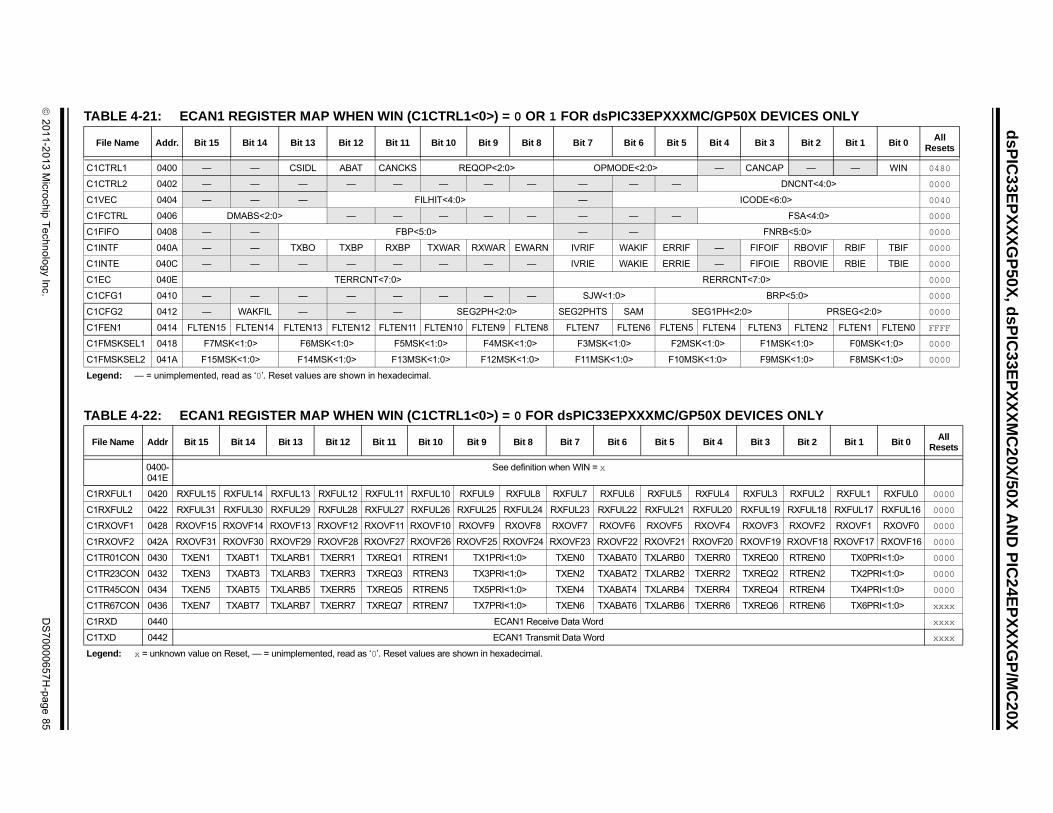
2
01
1-2
01
3 M
icroch
ip T
ech
no
log
y Inc.
DS
70
00
06
57
H-p
ag
e 8
5
ds
PIC
33E
PX
XX
GP
50X
, ds
PIC
33E
PX
XX
MC
20X
/50X
AN
D P
IC2
4EP
XX
XG
P/M
C2
0X
TA X DEVICES ONLY
Bit 3 Bit 2 Bit 1 Bit 0All
Resets
C1 CANCAP — — WIN 0480
C1 DNCNT<4:0> 0000
C1 CODE<6:0> 0040
C1 FSA<4:0> 0000
C1 FNRB<5:0> 0000
C1 FIFOIF RBOVIF RBIF TBIF 0000
C1 FIFOIE RBOVIE RBIE TBIE 0000
C1 <7:0> 0000
C1 BRP<5:0> 0000
C1 > PRSEG<2:0> 0000
C1 FLTEN3 FLTEN2 FLTEN1 FLTEN0 FFFF
C1 F1MSK<1:0> F0MSK<1:0> 0000
C1 F9MSK<1:0> F8MSK<1:0> 0000
Le
TA VICES ONLY
F Bit 3 Bit 2 Bit 1 Bit 0All
Resets
C1 RXFUL3 RXFUL2 RXFUL1 RXFUL0 0000
C1 XFUL19 RXFUL18 RXFUL17 RXFUL16 0000
C1 RXOVF3 RXOVF2 RXOVF1 RXOVF0 0000
C1 XOVF19 RXOVF18 RXOVF17 RXOVF16 0000
C1 TXREQ0 RTREN0 TX0PRI<1:0> 0000
C1 TXREQ2 RTREN2 TX2PRI<1:0> 0000
C1 TXREQ4 RTREN4 TX4PRI<1:0> 0000
C1 TXREQ6 RTREN6 TX6PRI<1:0> xxxx
C1 xxxx
C1 xxxx
Le
BLE 4-21: ECAN1 REGISTER MAP WHEN WIN (C1CTRL1<0>) = 0 OR 1 FOR dsPIC33EPXXXMC/GP50
File Name Addr. Bit 15 Bit 14 Bit 13 Bit 12 Bit 11 Bit 10 Bit 9 Bit 8 Bit 7 Bit 6 Bit 5 Bit 4
CTRL1 0400 — — CSIDL ABAT CANCKS REQOP<2:0> OPMODE<2:0> —
CTRL2 0402 — — — — — — — — — — —
VEC 0404 — — — FILHIT<4:0> — I
FCTRL 0406 DMABS<2:0> — — — — — — — —
FIFO 0408 — — FBP<5:0> — —
INTF 040A — — TXBO TXBP RXBP TXWAR RXWAR EWARN IVRIF WAKIF ERRIF —
INTE 040C — — — — — — — — IVRIE WAKIE ERRIE —
EC 040E TERRCNT<7:0> RERRCNT
CFG1 0410 — — — — — — — — SJW<1:0>
CFG2 0412 — WAKFIL — — — SEG2PH<2:0> SEG2PHTS SAM SEG1PH<2:0
FEN1 0414 FLTEN15 FLTEN14 FLTEN13 FLTEN12 FLTEN11 FLTEN10 FLTEN9 FLTEN8 FLTEN7 FLTEN6 FLTEN5 FLTEN4
FMSKSEL1 0418 F7MSK<1:0> F6MSK<1:0> F5MSK<1:0> F4MSK<1:0> F3MSK<1:0> F2MSK<1:0>
FMSKSEL2 041A F15MSK<1:0> F14MSK<1:0> F13MSK<1:0> F12MSK<1:0> F11MSK<1:0> F10MSK<1:0>
gend: — = unimplemented, read as ‘0’. Reset values are shown in hexadecimal.
BLE 4-22: ECAN1 REGISTER MAP WHEN WIN (C1CTRL1<0>) = 0 FOR dsPIC33EPXXXMC/GP50X DE
ile Name Addr Bit 15 Bit 14 Bit 13 Bit 12 Bit 11 Bit 10 Bit 9 Bit 8 Bit 7 Bit 6 Bit 5 Bit 4
0400-041E
See definition when WIN = x
RXFUL1 0420 RXFUL15 RXFUL14 RXFUL13 RXFUL12 RXFUL11 RXFUL10 RXFUL9 RXFUL8 RXFUL7 RXFUL6 RXFUL5 RXFUL4
RXFUL2 0422 RXFUL31 RXFUL30 RXFUL29 RXFUL28 RXFUL27 RXFUL26 RXFUL25 RXFUL24 RXFUL23 RXFUL22 RXFUL21 RXFUL20 R
RXOVF1 0428 RXOVF15 RXOVF14 RXOVF13 RXOVF12 RXOVF11 RXOVF10 RXOVF9 RXOVF8 RXOVF7 RXOVF6 RXOVF5 RXOVF4
RXOVF2 042A RXOVF31 RXOVF30 RXOVF29 RXOVF28 RXOVF27 RXOVF26 RXOVF25 RXOVF24 RXOVF23 RXOVF22 RXOVF21 RXOVF20 R
TR01CON 0430 TXEN1 TXABT1 TXLARB1 TXERR1 TXREQ1 RTREN1 TX1PRI<1:0> TXEN0 TXABAT0 TXLARB0 TXERR0
TR23CON 0432 TXEN3 TXABT3 TXLARB3 TXERR3 TXREQ3 RTREN3 TX3PRI<1:0> TXEN2 TXABAT2 TXLARB2 TXERR2
TR45CON 0434 TXEN5 TXABT5 TXLARB5 TXERR5 TXREQ5 RTREN5 TX5PRI<1:0> TXEN4 TXABAT4 TXLARB4 TXERR4
TR67CON 0436 TXEN7 TXABT7 TXLARB7 TXERR7 TXREQ7 RTREN7 TX7PRI<1:0> TXEN6 TXABAT6 TXLARB6 TXERR6
RXD 0440 ECAN1 Receive Data Word
TXD 0442 ECAN1 Transmit Data Word
gend: x = unknown value on Reset, — = unimplemented, read as ‘0’. Reset values are shown in hexadecimal.

ds
PIC
33E
PX
XX
GP
50X
, dsP
IC33
EP
XX
XM
C20
X/5
0X A
ND
PIC
24E
PX
XX
GP
/MC
20X
DS
70
00
06
57
H-p
ag
e 8
6
20
11
-20
13
Micro
chip
Te
chn
olo
gy In
c.
DEVICES ONLY
Bit 3 Bit 2 Bit 1 Bit 0All
Resets
F0BP<3:0> 0000
F4BP<3:0> 0000
F8BP<3:0> 0000
F12BP<3:0> 0000
MIDE — EID<17:16> xxxx
D<7:0> xxxx
MIDE — EID<17:16> xxxx
D<7:0> xxxx
MIDE — EID<17:16> xxxx
D<7:0> xxxx
EXIDE — EID<17:16> xxxx
D<7:0> xxxx
EXIDE — EID<17:16> xxxx
D<7:0> xxxx
EXIDE — EID<17:16> xxxx
D<7:0> xxxx
EXIDE — EID<17:16> xxxx
D<7:0> xxxx
EXIDE — EID<17:16> xxxx
D<7:0> xxxx
EXIDE — EID<17:16> xxxx
D<7:0> xxxx
EXIDE — EID<17:16> xxxx
D<7:0> xxxx
EXIDE — EID<17:16> xxxx
D<7:0> xxxx
EXIDE — EID<17:16> xxxx
D<7:0> xxxx
EXIDE — EID<17:16> xxxx
D<7:0> xxxx
EXIDE — EID<17:16> xxxx
D<7:0> xxxx
EXIDE — EID<17:16> xxxx
TABLE 4-23: ECAN1 REGISTER MAP WHEN WIN (C1CTRL1<0>) = 1 FOR dsPIC33EPXXXMC/GP50X
File Name Addr Bit 15 Bit 14 Bit 13 Bit 12 Bit 11 Bit 10 Bit 9 Bit 8 Bit 7 Bit 6 Bit 5 Bit 4
0400-041E
See definition when WIN = x
C1BUFPNT1 0420 F3BP<3:0> F2BP<3:0> F1BP<3:0>
C1BUFPNT2 0422 F7BP<3:0> F6BP<3:0> F5BP<3:0>
C1BUFPNT3 0424 F11BP<3:0> F10BP<3:0> F9BP<3:0>
C1BUFPNT4 0426 F15BP<3:0> F14BP<3:0> F13BP<3:0>
C1RXM0SID 0430 SID<10:3> SID<2:0> —
C1RXM0EID 0432 EID<15:8> EI
C1RXM1SID 0434 SID<10:3> SID<2:0> —
C1RXM1EID 0436 EID<15:8> EI
C1RXM2SID 0438 SID<10:3> SID<2:0> —
C1RXM2EID 043A EID<15:8> EI
C1RXF0SID 0440 SID<10:3> SID<2:0> —
C1RXF0EID 0442 EID<15:8> EI
C1RXF1SID 0444 SID<10:3> SID<2:0> —
C1RXF1EID 0446 EID<15:8> EI
C1RXF2SID 0448 SID<10:3> SID<2:0> —
C1RXF2EID 044A EID<15:8> EI
C1RXF3SID 044C SID<10:3> SID<2:0> —
C1RXF3EID 044E EID<15:8> EI
C1RXF4SID 0450 SID<10:3> SID<2:0> —
C1RXF4EID 0452 EID<15:8> EI
C1RXF5SID 0454 SID<10:3> SID<2:0> —
C1RXF5EID 0456 EID<15:8> EI
C1RXF6SID 0458 SID<10:3> SID<2:0> —
C1RXF6EID 045A EID<15:8> EI
C1RXF7SID 045C SID<10:3> SID<2:0> —
C1RXF7EID 045E EID<15:8> EI
C1RXF8SID 0460 SID<10:3> SID<2:0> —
C1RXF8EID 0462 EID<15:8> EI
C1RXF9SID 0464 SID<10:3> SID<2:0> —
C1RXF9EID 0466 EID<15:8> EI
C1RXF10SID 0468 SID<10:3> SID<2:0> —
C1RXF10EID 046A EID<15:8> EI
C1RXF11SID 046C SID<10:3> SID<2:0> —
Legend: x = unknown value on Reset, — = unimplemented, read as ‘0’. Reset values are shown in hexadecimal.

2
01
1-2
01
3 M
icroch
ip T
ech
no
log
y Inc.
DS
70
00
06
57
H-p
ag
e 8
7
ds
PIC
33E
PX
XX
GP
50X
, ds
PIC
33E
PX
XX
MC
20X
/50X
AN
D P
IC2
4EP
XX
XG
P/M
C2
0X
C1 > xxxx
C1 EXIDE — EID<17:16> xxxx
C1 > xxxx
C1 EXIDE — EID<17:16> xxxx
C1 > xxxx
C1 EXIDE — EID<17:16> xxxx
C1 > xxxx
C1 EXIDE — EID<17:16> xxxx
C1 > xxxx
TA VICES ONLY (CONTINUED)
F Bit 3 Bit 2 Bit 1 Bit 0All
Resets
Le
RXF11EID 046E EID<15:8> EID<7:0
RXF12SID 0470 SID<10:3> SID<2:0> —
RXF12EID 0472 EID<15:8> EID<7:0
RXF13SID 0474 SID<10:3> SID<2:0> —
RXF13EID 0476 EID<15:8> EID<7:0
RXF14SID 0478 SID<10:3> SID<2:0> —
RXF14EID 047A EID<15:8> EID<7:0
RXF15SID 047C SID<10:3> SID<2:0> —
RXF15EID 047E EID<15:8> EID<7:0
BLE 4-23: ECAN1 REGISTER MAP WHEN WIN (C1CTRL1<0>) = 1 FOR dsPIC33EPXXXMC/GP50X DE
ile Name Addr Bit 15 Bit 14 Bit 13 Bit 12 Bit 11 Bit 10 Bit 9 Bit 8 Bit 7 Bit 6 Bit 5 Bit 4
gend: x = unknown value on Reset, — = unimplemented, read as ‘0’. Reset values are shown in hexadecimal.
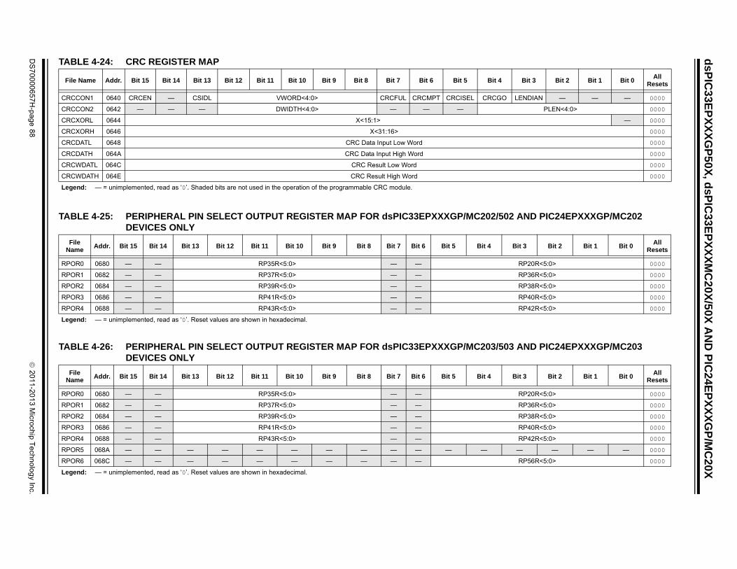
ds
PIC
33E
PX
XX
GP
50X
, dsP
IC33
EP
XX
XM
C20
X/5
0X A
ND
PIC
24E
PX
XX
GP
/MC
20X
DS
70
00
06
57
H-p
ag
e 8
8
20
11
-20
13
Micro
chip
Te
chn
olo
gy In
c.
02 AND PIC24EPXXXGP/MC202
03 AND PIC24EPXXXGP/MC203
Bit 3 Bit 2 Bit 1 Bit 0All
Resets
LENDIAN — — — 0000
PLEN<4:0> 0000
— 0000
0000
0000
0000
0000
0000
Bit 3 Bit 2 Bit 1 Bit 0All
Resets
RP20R<5:0> 0000
RP36R<5:0> 0000
RP38R<5:0> 0000
RP40R<5:0> 0000
RP42R<5:0> 0000
Bit 3 Bit 2 Bit 1 Bit 0All
Resets
RP20R<5:0> 0000
RP36R<5:0> 0000
RP38R<5:0> 0000
RP40R<5:0> 0000
RP42R<5:0> 0000
— — — — 0000
RP56R<5:0> 0000
TABLE 4-24: CRC REGISTER MAP
TABLE 4-25: PERIPHERAL PIN SELECT OUTPUT REGISTER MAP FOR dsPIC33EPXXXGP/MC202/5DEVICES ONLY
TABLE 4-26: PERIPHERAL PIN SELECT OUTPUT REGISTER MAP FOR dsPIC33EPXXXGP/MC203/5DEVICES ONLY
File Name Addr. Bit 15 Bit 14 Bit 13 Bit 12 Bit 11 Bit 10 Bit 9 Bit 8 Bit 7 Bit 6 Bit 5 Bit 4
CRCCON1 0640 CRCEN — CSIDL VWORD<4:0> CRCFUL CRCMPT CRCISEL CRCGO
CRCCON2 0642 — — — DWIDTH<4:0> — — —
CRCXORL 0644 X<15:1>
CRCXORH 0646 X<31:16>
CRCDATL 0648 CRC Data Input Low Word
CRCDATH 064A CRC Data Input High Word
CRCWDATL 064C CRC Result Low Word
CRCWDATH 064E CRC Result High Word
Legend: — = unimplemented, read as ‘0’. Shaded bits are not used in the operation of the programmable CRC module.
File Name
Addr. Bit 15 Bit 14 Bit 13 Bit 12 Bit 11 Bit 10 Bit 9 Bit 8 Bit 7 Bit 6 Bit 5 Bit 4
RPOR0 0680 — — RP35R<5:0> — —
RPOR1 0682 — — RP37R<5:0> — —
RPOR2 0684 — — RP39R<5:0> — —
RPOR3 0686 — — RP41R<5:0> — —
RPOR4 0688 — — RP43R<5:0> — —
Legend: — = unimplemented, read as ‘0’. Reset values are shown in hexadecimal.
File Name
Addr. Bit 15 Bit 14 Bit 13 Bit 12 Bit 11 Bit 10 Bit 9 Bit 8 Bit 7 Bit 6 Bit 5 Bit 4
RPOR0 0680 — — RP35R<5:0> — —
RPOR1 0682 — — RP37R<5:0> — —
RPOR2 0684 — — RP39R<5:0> — —
RPOR3 0686 — — RP41R<5:0> — —
RPOR4 0688 — — RP43R<5:0> — —
RPOR5 068A — — — — — — — — — — — —
RPOR6 068C — — — — — — — — — —
Legend: — = unimplemented, read as ‘0’. Reset values are shown in hexadecimal.

2
01
1-2
01
3 M
icroch
ip T
ech
no
log
y Inc.
DS
70
00
06
57
H-p
ag
e 8
9
ds
PIC
33E
PX
XX
GP
50X
, ds
PIC
33E
PX
XX
MC
20X
/50X
AN
D P
IC2
4EP
XX
XG
P/M
C2
0X
TA ND PIC24EPXXXGP/MC204
TA ND PIC24EPXXXGP/MC206
N 3 Bit 2 Bit 1 Bit 0
All Resets
RP P20R<5:0> 0000
RP P36R<5:0> 0000
RP P38R<5:0> 0000
RP P40R<5:0> 0000
RP P42R<5:0> 0000
RP P54R<5:0> 0000
RP P56R<5:0> 0000
Le
N 3 Bit 2 Bit 1 Bit 0
All Resets
RP P20R<5:0> 0000
RP P36R<5:0> 0000
RP P38R<5:0> 0000
RP P40R<5:0> 0000
RP P42R<5:0> 0000
RP P54R<5:0> 0000
RP P56R<5:0> 0000
RP — — — 0000
RP — — — 0000
RP P120R<5:0> 0000
Le
BLE 4-27: PERIPHERAL PIN SELECT OUTPUT REGISTER MAP FOR dsPIC33EPXXXGP/MC204/504 ADEVICES ONLY
BLE 4-28: PERIPHERAL PIN SELECT OUTPUT REGISTER MAP FOR dsPIC33EPXXXGP/MC206/506 ADEVICES ONLY
File ame
Addr. Bit 15 Bit 14 Bit 13 Bit 12 Bit 11 Bit 10 Bit 9 Bit 8 Bit 7 Bit 6 Bit 5 Bit 4 Bit
OR0 0680 — — RP35R<5:0> — — R
OR1 0682 — — RP37R<5:0> — — R
OR2 0684 — — RP39R<5:0> — — R
OR3 0686 — — RP41R<5:0> — — R
OR4 0688 — — RP43R<5:0> — — R
OR5 068A — — RP55R<5:0> — — R
OR6 068C — — RP57R<5:0> — — R
gend: — = unimplemented, read as ‘0’. Reset values are shown in hexadecimal.
File ame
Addr. Bit 15 Bit 14 Bit 13 Bit 12 Bit 11 Bit 10 Bit 9 Bit 8 Bit 7 Bit 6 Bit 5 Bit 4 Bit
OR0 0680 — — RP35R<5:0> — — R
OR1 0682 — — RP37R<5:0> — — R
OR2 0684 — — RP39R<5:0> — — R
OR3 0686 — — RP41R<5:0> — — R
OR4 0688 — — RP43R<5:0> — — R
OR5 068A — — RP55R<5:0> — — R
OR6 068C — — RP57R<5:0> — — R
OR7 068E — — RP97R<5:0> — — — — —
OR8 0690 — — RP118R<5:0> — — — — —
OR9 0692 — — — — — — — — — — R
gend: — = unimplemented, read as ‘0’. Reset values are shown in hexadecimal.
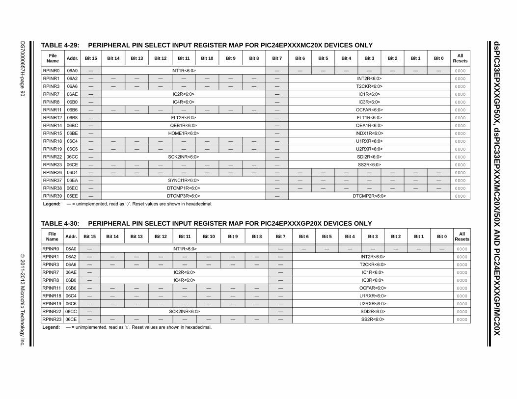
ds
PIC
33E
PX
XX
GP
50X
, dsP
IC33
EP
XX
XM
C20
X/5
0X A
ND
PIC
24E
PX
XX
GP
/MC
20X
DS
70
00
06
57
H-p
ag
e 9
0
20
11
-20
13
Micro
chip
Te
chn
olo
gy In
c.
ONLY
Bit 3 Bit 2 Bit 1 Bit 0All
Resets
— — — — 0000
INT2R<6:0> 0000
T2CKR<6:0> 0000
IC1R<6:0> 0000
IC3R<6:0> 0000
OCFAR<6:0> 0000
FLT1R<6:0> 0000
QEA1R<6:0> 0000
INDX1R<6:0> 0000
U1RXR<6:0> 0000
U2RXR<6:0> 0000
SDI2R<6:0> 0000
SS2R<6:0> 0000
— — — — 0000
— — — — 0000
— — — — 0000
DTCMP2R<6:0> 0000
ONLY
Bit 3 Bit 2 Bit 1 Bit 0All
Resets
— — — — 0000
INT2R<6:0> 0000
T2CKR<6:0> 0000
IC1R<6:0> 0000
IC3R<6:0> 0000
OCFAR<6:0> 0000
U1RXR<6:0> 0000
U2RXR<6:0> 0000
SDI2R<6:0> 0000
SS2R<6:0> 0000
TABLE 4-29: PERIPHERAL PIN SELECT INPUT REGISTER MAP FOR PIC24EPXXXMC20X DEVICES
File Name
Addr. Bit 15 Bit 14 Bit 13 Bit 12 Bit 11 Bit 10 Bit 9 Bit 8 Bit 7 Bit 6 Bit 5 Bit 4
RPINR0 06A0 — INT1R<6:0> — — — —
RPINR1 06A2 — — — — — — — — —
RPINR3 06A6 — — — — — — — — —
RPINR7 06AE — IC2R<6:0> —
RPINR8 06B0 — IC4R<6:0> —
RPINR11 06B6 — — — — — — — — —
RPINR12 06B8 — FLT2R<6:0> —
RPINR14 06BC — QEB1R<6:0> —
RPINR15 06BE — HOME1R<6:0> —
RPINR18 06C4 — — — — — — — — —
RPINR19 06C6 — — — — — — — — —
RPINR22 06CC — SCK2INR<6:0> —
RPINR23 06CE — — — — — — — — —
RPINR26 06D4 — — — — — — — — — — — —
RPINR37 06EA — SYNCI1R<6:0> — — — —
RPINR38 06EC — DTCMP1R<6:0> — — — —
RPINR39 06EE — DTCMP3R<6:0> —
Legend: — = unimplemented, read as ‘0’. Reset values are shown in hexadecimal.
TABLE 4-30: PERIPHERAL PIN SELECT INPUT REGISTER MAP FOR PIC24EPXXXGP20X DEVICES
File Name
Addr. Bit 15 Bit 14 Bit 13 Bit 12 Bit 11 Bit 10 Bit 9 Bit 8 Bit 7 Bit 6 Bit 5 Bit 4
RPINR0 06A0 — INT1R<6:0> — — — —
RPINR1 06A2 — — — — — — — — —
RPINR3 06A6 — — — — — — — — —
RPINR7 06AE — IC2R<6:0> —
RPINR8 06B0 — IC4R<6:0> —
RPINR11 06B6 — — — — — — — — —
RPINR18 06C4 — — — — — — — — —
RPINR19 06C6 — — — — — — — — —
RPINR22 06CC — SCK2INR<6:0> —
RPINR23 06CE — — — — — — — — —
Legend: — = unimplemented, read as ‘0’. Reset values are shown in hexadecimal.

2
01
1-2
01
3 M
icroch
ip T
ech
no
log
y Inc.
DS
70
00
06
57
H-p
ag
e 9
1
ds
PIC
33E
PX
XX
GP
50X
, ds
PIC
33E
PX
XX
MC
20X
/50X
AN
D P
IC2
4EP
XX
XG
P/M
C2
0X
TA NLY
Bit 3 Bit 2 Bit 1 Bit 0All
Resets
RP — — — — 0000
RP 2R<6:0> 0000
RP KR<6:0> 0000
RP R<6:0> 0000
RP R<6:0> 0000
RP AR<6:0> 0000
RP XR<6:0> 0000
RP XR<6:0> 0000
RP 2R<6:0> 0000
RP R<6:0> 0000
RP XR<6:0> 0000
Le
TA NLY
Fi Bit 3 Bit 2 Bit 1 Bit 0All
Resets
RP — — — — 0000
RP 2R<6:0> 0000
RP KR<6:0> 0000
RP R<6:0> 0000
RP R<6:0> 0000
RP AR<6:0> 0000
RP 1R<6:0> 0000
RP 1R<6:0> 0000
RP X1R<6:0> 0000
RP XR<6:0> 0000
RP XR<6:0> 0000
RP I2R<6:0> 0000
RP 2R<6:0> 0000
RP XR<6:0> 0000
RP — — — — 0000
RP — — — — 0000
RP P2R<6:0> 0000
Le
BLE 4-31: PERIPHERAL PIN SELECT INPUT REGISTER MAP FOR dsPIC33EPXXXGP50X DEVICES O
File Name
Addr. Bit 15 Bit 14 Bit 13 Bit 12 Bit 11 Bit 10 Bit 9 Bit 8 Bit 7 Bit 6 Bit 5 Bit 4
INR0 06A0 — INT1R<6:0> — — — —
INR1 06A2 — — — — — — — — — INT
INR3 06A6 — — — — — — — — — T2C
INR7 06AE — IC2R<6:0> — IC1
INR8 06B0 — IC4R<6:0> — IC3
INR11 06B6 — — — — — — — — — OCF
INR18 06C4 — — — — — — — — — U1R
INR19 06C6 — — — — — — — — — U2R
INR22 06CC — SCK2INR<6:0> — SDI
INR23 06CE — — — — — — — — — SS2
INR26 06D4 — — — — — — — — — C1R
gend: — = unimplemented, read as ‘0’. Reset values are shown in hexadecimal.
BLE 4-32: PERIPHERAL PIN SELECT INPUT REGISTER MAP FOR dsPIC33EPXXXMC50X DEVICES O
le Name Addr. Bit 15 Bit 14 Bit 13 Bit 12 Bit 11 Bit 10 Bit 9 Bit 8 Bit 7 Bit 6 Bit 5 Bit 4
INR0 06A0 — INT1R<6:0> — — — —
INR1 06A2 — — — — — — — — — INT
INR3 06A6 — — — — — — — — — T2C
INR7 06AE — IC2R<6:0> — IC1
INR8 06B0 — IC4R<6:0> — IC3
INR11 06B6 — — — — — — — — — OCF
INR12 06B8 — FLT2R<6:0> — FLT
INR14 06BC — QEB1R<6:0> — QEA
INR15 06BE — HOME1R<6:0> — IND
INR18 06C4 — — — — — — — — — U1R
INR19 06C6 — — — — — — — — — U2R
INR22 06CC — SCK2INR<6:0> — SD
INR23 06CE — — — — — — — — — SS
INR26 06D4 — — — — — — — — — C1R
INR37 06EA — SYNCI1R<6:0> — — — —
INR38 06EC — DTCMP1R<6:0> — — — —
INR39 06EE — DTCMP3R<6:0> — DTCM
gend: — = unimplemented, read as ‘0’. Reset values are shown in hexadecimal.
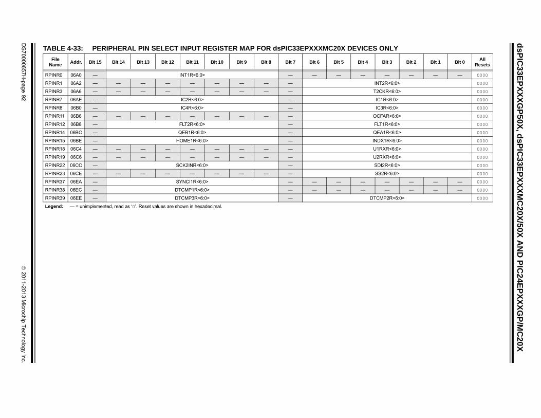
ds
PIC
33E
PX
XX
GP
50X
, dsP
IC33
EP
XX
XM
C20
X/5
0X A
ND
PIC
24E
PX
XX
GP
/MC
20X
DS
70
00
06
57
H-p
ag
e 9
2
20
11
-20
13
Micro
chip
Te
chn
olo
gy In
c.
S ONLY
Bit 3 Bit 2 Bit 1 Bit 0All
Resets
— — — — 0000
INT2R<6:0> 0000
T2CKR<6:0> 0000
IC1R<6:0> 0000
IC3R<6:0> 0000
OCFAR<6:0> 0000
FLT1R<6:0> 0000
QEA1R<6:0> 0000
INDX1R<6:0> 0000
U1RXR<6:0> 0000
U2RXR<6:0> 0000
SDI2R<6:0> 0000
SS2R<6:0> 0000
— — — — 0000
— — — — 0000
DTCMP2R<6:0> 0000
TABLE 4-33: PERIPHERAL PIN SELECT INPUT REGISTER MAP FOR dsPIC33EPXXXMC20X DEVICE
File Name
Addr. Bit 15 Bit 14 Bit 13 Bit 12 Bit 11 Bit 10 Bit 9 Bit 8 Bit 7 Bit 6 Bit 5 Bit 4
RPINR0 06A0 — INT1R<6:0> — — — —
RPINR1 06A2 — — — — — — — — —
RPINR3 06A6 — — — — — — — — —
RPINR7 06AE — IC2R<6:0> —
RPINR8 06B0 — IC4R<6:0> —
RPINR11 06B6 — — — — — — — — —
RPINR12 06B8 — FLT2R<6:0> —
RPINR14 06BC — QEB1R<6:0> —
RPINR15 06BE — HOME1R<6:0> —
RPINR18 06C4 — — — — — — — — —
RPINR19 06C6 — — — — — — — — —
RPINR22 06CC — SCK2INR<6:0> —
RPINR23 06CE — — — — — — — — —
RPINR37 06EA — SYNCI1R<6:0> — — — —
RPINR38 06EC — DTCMP1R<6:0> — — — —
RPINR39 06EE — DTCMP3R<6:0> —
Legend: — = unimplemented, read as ‘0’. Reset values are shown in hexadecimal.

2
01
1-2
01
3 M
icroch
ip T
ech
no
log
y Inc.
DS
70
00
06
57
H-p
ag
e 9
3
ds
PIC
33E
PX
XX
GP
50X
, ds
PIC
33E
PX
XX
MC
20X
/50X
AN
D P
IC2
4EP
XX
XG
P/M
C2
0X
TA
TA
TA
Fi Bit 3 Bit 2 Bit 1 Bit 0All
Resets
NV NVMOP<3:0> 0000
NV 0000
NV 23:16> 0000
NV 7:0> 0000
Leg
Fil Bit 3 Bit 2 Bit 1 Bit 0All
Resets
RC SLEEP IDLE BOR POR Note 1
OS CF — — OSWEN Note 2
CLK PLLPRE<4:0> 0030
PLL 0030
OS TUN<5:0> 0000
LegNot
Fil Bit 3 Bit 2 Bit 1 Bit 0All
Resets
RE — — — — 0000
Leg
BLE 4-34: NVM REGISTER MAP
BLE 4-35: SYSTEM CONTROL REGISTER MAP
BLE 4-36: REFERENCE CLOCK REGISTER MAP
le Name Addr. Bit 15 Bit 14 Bit 13 Bit 12 Bit 11 Bit 10 Bit 9 Bit 8 Bit 7 Bit 6 Bit 5 Bit 4
MCON 0728 WR WREN WRERR NVMSIDL — — — — — — — —
MADRL 072A NVMADR<15:0>
MADRH 072C — — — — — — — — NVMADR<
MKEY 072E — — — — — — — — NVMKEY<
end: — = unimplemented, read as ‘0’. Reset values are shown in hexadecimal.
e Name Addr. Bit 15 Bit 14 Bit 13 Bit 12 Bit 11 Bit 10 Bit 9 Bit 8 Bit 7 Bit 6 Bit 5 Bit 4
ON 0740 TRAPR IOPUWR — — VREGSF — CM VREGS EXTR SWR SWDTEN WDTO
CCON 0742 — COSC<2:0> — NOSC<2:0> CLKLOCK IOLOCK LOCK —
DIV 0744 ROI DOZE<2:0> DOZEN FRCDIV<2:0> PLLPOST<1:0> —
FBD 0746 — — — — — — — PLLDIV<8:0>
CTUN 0748 — — — — — — — — — —
end: — = unimplemented, read as ‘0’. Reset values are shown in hexadecimal.e 1: RCON register Reset values are dependent on the type of Reset.
2: OSCCON register Reset values are dependent on the Configuration Fuses.
e Name Addr. Bit 15 Bit 14 Bit 13 Bit 12 Bit 11 Bit 10 Bit 9 Bit 8 Bit 7 Bit 6 Bit 5 Bit 4
FOCON 074E ROON — ROSSLP ROSEL RODIV<3:0> — — — —
end: — = unimplemented, read as ‘0’. Reset values are shown in hexadecimal.
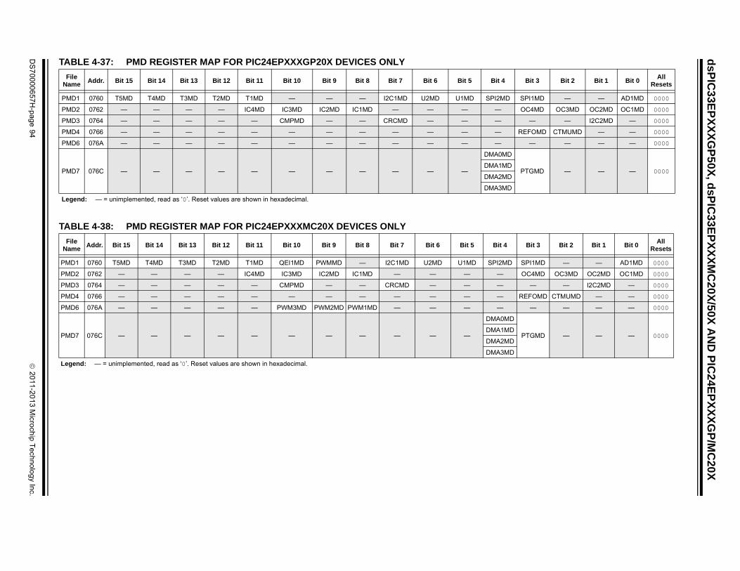
ds
PIC
33E
PX
XX
GP
50X
, dsP
IC33
EP
XX
XM
C20
X/5
0X A
ND
PIC
24E
PX
XX
GP
/MC
20X
DS
70
00
06
57
H-p
ag
e 9
4
20
11
-20
13
Micro
chip
Te
chn
olo
gy In
c.
Bit 3 Bit 2 Bit 1 Bit 0All
Resets
D SPI1MD — — AD1MD 0000
OC4MD OC3MD OC2MD OC1MD 0000
— — I2C2MD — 0000
REFOMD CTMUMD — — 0000
— — — — 0000
D
PTGMD — — — 0000D
D
D
Bit 3 Bit 2 Bit 1 Bit 0All
Resets
D SPI1MD — — AD1MD 0000
OC4MD OC3MD OC2MD OC1MD 0000
— — I2C2MD — 0000
REFOMD CTMUMD — — 0000
— — — — 0000
D
PTGMD — — — 0000D
D
D
TABLE 4-37: PMD REGISTER MAP FOR PIC24EPXXXGP20X DEVICES ONLY
TABLE 4-38: PMD REGISTER MAP FOR PIC24EPXXXMC20X DEVICES ONLY
FileName
Addr. Bit 15 Bit 14 Bit 13 Bit 12 Bit 11 Bit 10 Bit 9 Bit 8 Bit 7 Bit 6 Bit 5 Bit 4
PMD1 0760 T5MD T4MD T3MD T2MD T1MD — — — I2C1MD U2MD U1MD SPI2M
PMD2 0762 — — — — IC4MD IC3MD IC2MD IC1MD — — — —
PMD3 0764 — — — — — CMPMD — — CRCMD — — —
PMD4 0766 — — — — — — — — — — — —
PMD6 076A — — — — — — — — — — — —
PMD7 076C — — — — — — — — — — —
DMA0M
DMA1M
DMA2M
DMA3M
Legend: — = unimplemented, read as ‘0’. Reset values are shown in hexadecimal.
FileName
Addr. Bit 15 Bit 14 Bit 13 Bit 12 Bit 11 Bit 10 Bit 9 Bit 8 Bit 7 Bit 6 Bit 5 Bit 4
PMD1 0760 T5MD T4MD T3MD T2MD T1MD QEI1MD PWMMD — I2C1MD U2MD U1MD SPI2M
PMD2 0762 — — — — IC4MD IC3MD IC2MD IC1MD — — — —
PMD3 0764 — — — — — CMPMD — — CRCMD — — —
PMD4 0766 — — — — — — — — — — — —
PMD6 076A — — — — — PWM3MD PWM2MD PWM1MD — — — —
PMD7 076C — — — — — — — — — — —
DMA0M
DMA1M
DMA2M
DMA3M
Legend: — = unimplemented, read as ‘0’. Reset values are shown in hexadecimal.

2
01
1-2
01
3 M
icroch
ip T
ech
no
log
y Inc.
DS
70
00
06
57
H-p
ag
e 9
5
ds
PIC
33E
PX
XX
GP
50X
, ds
PIC
33E
PX
XX
MC
20X
/50X
AN
D P
IC2
4EP
XX
XG
P/M
C2
0X
TA
TA
FNa
Bit 3 Bit 2 Bit 1 Bit 0All
Resets
PM PI1MD — C1MD AD1MD 0000
PM C4MD OC3MD OC2MD OC1MD 0000
PM — — I2C2MD — 0000
PM EFOMD CTMUMD — — 0000
PM — — — — 0000
PM TGMD — — — 0000
Leg
FNa
Bit 3 Bit 2 Bit 1 Bit 0All
Resets
PM PI1MD — C1MD AD1MD 0000
PM OC4MD OC3MD OC2MD OC1MD 0000
PM — — I2C2MD — 0000
PM EFOMD CTMUMD — — 0000
PM — — — — 0000
PM PTGMD — — — 0000
Leg
BLE 4-39: PMD REGISTER MAP FOR dsPIC33EPXXXGP50X DEVICES ONLY
BLE 4-40: PMD REGISTER MAP FOR dsPIC33EPXXXMC50X DEVICES ONLY
ileme
Addr. Bit 15 Bit 14 Bit 13 Bit 12 Bit 11 Bit 10 Bit 9 Bit 8 Bit 7 Bit 6 Bit 5 Bit 4
D1 0760 T5MD T4MD T3MD T2MD T1MD — — — I2C1MD U2MD U1MD SPI2MD S
D2 0762 — — — — IC4MD IC3MD IC2MD IC1MD — — — — O
D3 0764 — — — — — CMPMD — — CRCMD — — —
D4 0766 — — — — — — — — — — — — R
D6 076A — — — — — — — — — — — —
D7 076C — — — — — — — — — — —
DMA0MD
PDMA1MD
DMA2MD
DMA3MD
end: — = unimplemented, read as ‘0’. Reset values are shown in hexadecimal.
ileme
Addr. Bit 15 Bit 14 Bit 13 Bit 12 Bit 11 Bit 10 Bit 9 Bit 8 Bit 7 Bit 6 Bit 5 Bit 4
D1 0760 T5MD T4MD T3MD T2MD T1MD QEI1MD PWMMD — I2C1MD U2MD U1MD SPI2MD S
D2 0762 — — — — IC4MD IC3MD IC2MD IC1MD — — — —
D3 0764 — — — — — CMPMD — — CRCMD — — —
D4 0766 — — — — — — — — — — — — R
D6 076A — — — — — PWM3MD PWM2MD PWM1MD — — — —
D7 076C — — — — — — — — — — —
DMA0MD
DMA1MD
DMA2MD
DMA3MD
end: — = unimplemented, read as ‘0’. Reset values are shown in hexadecimal.

ds
PIC
33E
PX
XX
GP
50X
, dsP
IC33
EP
XX
XM
C20
X/5
0X A
ND
PIC
24E
PX
XX
GP
/MC
20X
DS
70
00
06
57
H-p
ag
e 9
6
20
11
-20
13
Micro
chip
Te
chn
olo
gy In
c.
Bit 3 Bit 2 Bit 1 Bit 0All
Resets
D SPI1MD — — AD1MD 0000
OC4MD OC3MD OC2MD OC1MD 0000
— — I2C2MD — 0000
REFOMD CTMUMD — — 0000
— — — — 0000
MD
PTGMD — — — 0000MD
MD
MD
TABLE 4-41: PMD REGISTER MAP FOR dsPIC33EPXXXMC20X DEVICES ONLY
FileName
Addr. Bit 15 Bit 14 Bit 13 Bit 12 Bit 11 Bit 10 Bit 9 Bit 8 Bit 7 Bit 6 Bit 5 Bit 4
PMD1 0760 T5MD T4MD T3MD T2MD T1MD QEI1MD PWMMD — I2C1MD U2MD U1MD SPI2M
PMD2 0762 — — — — IC4MD IC3MD IC2MD IC1MD — — — —
PMD3 0764 — — — — — CMPMD — — CRCMD — — —
PMD4 0766 — — — — — — — — — — — —
PMD6 076A — — — — — PWM3MD PWM2MD PWM1MD — — — —
PMD7 076C — — — — — — — — — — —
DMA0
DMA1
DMA2
DMA3
Legend: — = unimplemented, read as ‘0’. Reset values are shown in hexadecimal.

2
01
1-2
01
3 M
icroch
ip T
ech
no
log
y Inc.
DS
70
00
06
57
H-p
ag
e 9
7
ds
PIC
33E
PX
XX
GP
50X
, ds
PIC
33E
PX
XX
MC
20X
/50X
AN
D P
IC2
4EP
XX
XG
P/M
C2
0X
TA
TA
Bit 3 Bit 2 Bit 1 Bit 0All
Resets
CM C4OUT C3OUT C2OUT C1OUT 0000
CV CVR<3:0> 0000
CM — — CCH<1:0> 0000
CM SELSRCA<3:0> 0000
CM ABEN ABNEN AAEN AANEN 0000
CM CFLTREN CFDIV<2:0> 0000
CM — — CCH<1:0> 0000
CM SELSRCA<3:0> 0000
CM ABEN ABNEN AAEN AANEN 0000
CM CFLTREN CFDIV<2:0> 0000
CM — — CCH<1:0> 0000
CM SELSRCA<3:0> 0000
CM ABEN ABNEN AAEN AANEN 0000
CM CFLTREN CFDIV<2:0> 0000
CM — — CCH<1:0> 0000
CM SELSRCA<3:0> 0000
CM ABEN ABNEN AAEN AANEN 0000
CM CFLTREN CFDIV<2:0> 0000
LegNo
TA
Fi Bit 4 Bit 3 Bit 2 Bit 1 Bit 0All
Resets
CT — — — — — 0000
CT DG2SEL<3:0> — — 0000
CT — — — — — 0000
Le
Fi Bit 3 Bit 2 Bit 1 Bit 0All
Resets
JD xxxx
JD 0000
Le
BLE 4-42: OP AMP/COMPARATOR REGISTER MAP
BLE 4-44: JTAG INTERFACE REGISTER MAP
File Name Addr. Bit 15 Bit 14 Bit 13 Bit 12 Bit 11 Bit 10 Bit 9 Bit 8 Bit 7 Bit 6 Bit 5 Bit 4
STAT 0A80 PSIDL — — — C4EVT C3EVT C2EVT C1EVT — — — —
RCON 0A82 — CVR2OE — — — VREFSEL — — CVREN CVR1OE CVRR CVRSS
1CON 0A84 CON COE CPOL — — OPMODE CEVT COUT EVPOL<1:0> — CREF
1MSKSRC 0A86 — — — — SELSRCC<3:0> SELSRCB<3:0>
1MSKCON 0A88 HLMS — OCEN OCNEN OBEN OBNEN OAEN OANEN NAGS PAGS ACEN ACNEN
1FLTR 0A8A — — — — — — — — — CFSEL<2:0>
2CON 0A8C CON COE CPOL — — OPMODE CEVT COUT EVPOL<1:0> — CREF
2MSKSRC 0A8E — — — — SELSRCC<3:0> SELSRCB<3:0>
2MSKCON 0A90 HLMS — OCEN OCNEN OBEN OBNEN OAEN OANEN NAGS PAGS ACEN ACNEN
2FLTR 0A92 — — — — — — — — — CFSEL<2:0>
3CON(1) 0A94 CON COE CPOL — — OPMODE CEVT COUT EVPOL<1:0> — CREF
3MSKSRC(1) 0A96 — — — — SELSRCC<3:0> SELSRCB<3:0>
3MSKCON(1) 0A98 HLMS — OCEN OCNEN OBEN OBNEN OAEN OANEN NAGS PAGS ACEN ACNEN
3FLTR(1) 0A9A — — — — — — — — — CFSEL<2:0>
4CON 0A9C CON COE CPOL — — — CEVT COUT EVPOL<1:0> — CREF
4MSKSRC 0A9E — — — — SELSRCC<3:0> SELSRCB<3:0>
4MSKCON 0AA0 HLMS — OCEN OCNEN OBEN OBNEN OAEN OANEN NAGS PAGS ACEN ACNEN
4FLTR 0AA2 — — — — — — — — — CFSEL<2:0>
end: — = unimplemented, read as ‘0’. Reset values are shown in hexadecimal.te 1: These registers are unavailable on dsPIC33EPXXXGP502/MC502/MC202 and PIC24EP256GP/MC202 (28-pin) devices.
BLE 4-43: CTMU REGISTER MAP
le Name Addr. Bit 15 Bit 14 Bit 13 Bit 12 Bit 11 Bit 10 Bit 9 Bit 8 Bit 7 Bit 6 Bit 5
MUCON1 033A CTMUEN — CTMUSIDL TGEN EDGEN EDGSEQEN IDISSEN CTTRIG — — —
MUCON2 033C EDG1MOD EDG1POL EDG1SEL<3:0> EDG2STAT EDG1STAT EDG2MOD EDG2POL E
MUICON 033E ITRIM<5:0> IRNG<1:0> — — —
gend: — = unimplemented, read as ‘0’. Reset values are shown in hexadecimal.
le Name Addr Bit 15 Bit 14 Bit 13 Bit 12 Bit 11 Bit 10 Bit 9 Bit 8 Bit 7 Bit 6 Bit 5 Bit 4
ATAH 0FF0 — — — — JDATAH<27:16>
ATAL 0FF2 JDATAL<15:0>
gend: x = unknown value on Reset, — = unimplemented, read as ‘0’. Reset values are shown in hexadecimal.

ds
PIC
33E
PX
XX
GP
50X
, dsP
IC33
EP
XX
XM
C20
X/5
0X A
ND
PIC
24E
PX
XX
GP
/MC
20X
DS
70
00
06
57
H-p
ag
e 9
8
20
11
-20
13
Micro
chip
Te
chn
olo
gy In
c.
t 4 Bit 3 Bit 2 Bit 1 Bit 0All
Resets
> — — MODE<1:0> 0000
QSEL<7:0> 00FF
0000
TA<23:16> 0000
0000
TB<23:16> 0000
0000
0000
> — — MODE<1:0> 0000
QSEL<7:0> 00FF
0000
TA<23:16> 0000
0000
TB<23:16> 0000
0000
0000
> — — MODE<1:0> 0000
QSEL<7:0> 00FF
0000
TA<23:16> 0000
0000
TB<23:16> 0000
0000
0000
> — — MODE<1:0> 0000
QSEL<7:0> 00FF
0000
TA<23:16> 0000
0000
TB<23:16> 0000
0000
0000
PWCOL3 PWCOL2 PWCOL1 PWCOL0 0000
RQCOL3 RQCOL2 RQCOL1 RQCOL0 0000
PPST3 PPST2 PPST1 PPST0 0000
LSTCH<3:0> 000F
0000
ADR<23:16> 0000
TABLE 4-45: DMAC REGISTER MAP
File Name Addr. Bit 15 Bit 14 Bit 13 Bit 12 Bit 11 Bit 10 Bit 9 Bit 8 Bit 7 Bit 6 Bit 5 Bi
DMA0CON 0B00 CHEN SIZE DIR HALF NULLW — — — — — AMODE<1:0
DMA0REQ 0B02 FORCE — — — — — — — IR
DMA0STAL 0B04 STA<15:0>
DMA0STAH 0B06 — — — — — — — — S
DMA0STBL 0B08 STB<15:0>
DMA0STBH 0B0A — — — — — — — — S
DMA0PAD 0B0C PAD<15:0>
DMA0CNT 0B0E — — CNT<13:0>
DMA1CON 0B10 CHEN SIZE DIR HALF NULLW — — — — — AMODE<1:0
DMA1REQ 0B12 FORCE — — — — — — — IR
DMA1STAL 0B14 STA<15:0>
DMA1STAH 0B16 — — — — — — — — S
DMA1STBL 0B18 STB<15:0>
DMA1STBH 0B1A — — — — — — — — S
DMA1PAD 0B1C PAD<15:0>
DMA1CNT 0B1E — — CNT<13:0>
DMA2CON 0B20 CHEN SIZE DIR HALF NULLW — — — — — AMODE<1:0
DMA2REQ 0B22 FORCE — — — — — — — IR
DMA2STAL 0B24 STA<15:0>
DMA2STAH 0B26 — — — — — — — — S
DMA2STBL 0B28 STB<15:0>
DMA2STBH 0B2A — — — — — — — — S
DMA2PAD 0B2C PAD<15:0>
DMA2CNT 0B2E — — CNT<13:0>
DMA3CON 0B30 CHEN SIZE DIR HALF NULLW — — — — — AMODE<1:0
DMA3REQ 0B32 FORCE — — — — — — — IR
DMA3STAL 0B34 STA<15:0>
DMA3STAH 0B36 — — — — — — — — S
DMA3STBL 0B38 STB<15:0>
DMA3STBH 0B3A — — — — — — — — S
DMA3PAD 0B3C PAD<15:0>
DMA3CNT 0B3E — — CNT<13:0>
DMAPWC 0BF0 — — — — — — — — — — — —
DMARQC 0BF2 — — — — — — — — — — — —
DMAPPS 0BF4 — — — — — — — — — — — —
DMALCA 0BF6 — — — — — — — — — — — —
DSADRL 0BF8 DSADR<15:0>
DSADRH 0BFA — — — — — — — — DS
Legend: — = unimplemented, read as ‘0’. Reset values are shown in hexadecimal.

2
01
1-2
01
3 M
icroch
ip T
ech
no
log
y Inc.
DS
70
00
06
57
H-p
ag
e 9
9
ds
PIC
33E
PX
XX
GP
50X
, ds
PIC
33E
PX
XX
MC
20X
/50X
AN
D P
IC2
4EP
XX
XG
P/M
C2
0X
TA EVICES ONLY
TA EVICES ONLY
TA EVICES ONLY
NBit 3 Bit 2 Bit 1 Bit 0
All Resets
TR — — TRISA1 TRISA0 1F93
PO — — RA1 RA0 0000
LA — — LA1TA1 LA0TA0 0000
OD — — ODCA1 ODCA0 0000
CN — — CNIEA1 CNIEA0 0000
CN — — CNPUA1 CNPUA0 0000
CN — — CNPDA1 CNPDA0 0000
AN — — ANSA1 ANSA0 1813
Le
NBit 3 Bit 2 Bit 1 Bit 0
All Resets
TR TRISB3 TRISB2 TRISB1 TRISB0 FFFF
PO RB3 RB2 RB1 RB0 xxxx
LA LATB3 LATB2 LATB1 LATB0 xxxx
OD ODCB3 ODCB2 ODCB1 ODCB0 0000
CN CNIEB3 CNIEB2 CNIEB1 CNIEB0 0000
CN CNPUB3 CNPUB2 CNPUB1 CNPUB0 0000
CN CNPDB3 CNPDB2 CNPDB1 CNPDB0 0000
AN ANSB3 ANSB2 ANSB1 ANSB0 010F
Le
NBit 3 Bit 2 Bit 1 Bit 0
All Resets
TR RISC3 TRISC2 TRISC1 TRISC0 BFFF
PO RC3 RC2 RC1 RC0 xxxx
LA LATC3 LATC2 LATC1 LATC0 xxxx
OD DCC3 ODCC2 ODCC1 ODCC0 0000
CN NIEC3 CNIEC2 CNIEC1 CNIEC0 0000
CN NPUC3 CNPUC2 CNPUC1 CNPUC0 0000
CN NPDC3 CNPDC2 CNPDC1 CNPDC0 0000
AN — ANSC2 ANSC1 ANSC0 0807
Le
BLE 4-46: PORTA REGISTER MAP FOR PIC24EPXXXGP/MC206 AND dsPIC33EPXXXGP/MC206/506 D
BLE 4-47: PORTB REGISTER MAP FOR PIC24EPXXXGP/MC206 AND dsPIC33EPXXXGP/MC206/506 D
BLE 4-48: PORTC REGISTER MAP FOR PIC24EPXXXGP/MC206 AND dsPIC33EPXXXGP/MC206/506 D
File ame
Addr. Bit 15 Bit 14 Bit 13 Bit 12 Bit 11 Bit 10 Bit 9 Bit 8 Bit 7 Bit 6 Bit 5 Bit 4
ISA 0E00 — — — TRISA12 TRISA11 TRISA10 TRISA9 TRISA8 TRISA7 — — TRISA4
RTA 0E02 — — — RA12 RA11 RA10 RA9 RA8 RA7 — — RA4
TA 0E04 — — — LATA12 LATA11 LATA10 LATA9 LATA8 LATA7 — — LATA4
CA 0E06 — — — ODCA12 ODCA11 ODCA10 ODCA9 ODCA8 ODCA7 — — ODCA4
ENA 0E08 — — — CNIEA12 CNIEA11 CNIEA10 CNIEA9 CNIEA8 CNIEA7 — — CNIEA4
PUA 0E0A — — — CNPUA12 CNPUA11 CNPUA10 CNPUA9 CNPUA8 CNPUA7 — — CNPUA4
PDA 0E0C — — — CNPDA12 CNPDA11 CNPDA10 CNPDA9 CNPDA8 CNPDA7 — — CNPDA4
SELA 0E0E — — — ANSA12 ANSA11 — — — — — — ANSA4
gend: — = unimplemented, read as ‘0’. Reset values are shown in hexadecimal.
File ame
Addr. Bit 15 Bit 14 Bit 13 Bit 12 Bit 11 Bit 10 Bit 9 Bit 8 Bit 7 Bit 6 Bit 5 Bit 4
ISB 0E10 TRISB15 TRISB14 TRISB13 TRISB12 TRISB11 TRISB10 TRISB9 TRISB8 TRISB7 TRISB6 TRISB5 TRISB4
RTB 0E12 RB15 RB14 RB13 RB12 RB11 RB10 RB9 RB8 RB7 RB6 RB5 RB4
TB 0E14 LATB15 LATB14 LATB13 LATB12 LATB11 LATB10 LATB9 LATB8 LATB7 LATB6 LATB5 LATB4
CB 0E16 ODCB15 ODCB14 ODCB13 ODCB12 ODCB11 ODCB10 ODCB9 ODCB8 ODCB7 ODCB6 ODCB5 ODCB4
ENB 0E18 CNIEB15 CNIEB14 CNIEB13 CNIEB12 CNIEB11 CNIEB10 CNIEB9 CNIEB8 CNIEB7 CNIEB6 CNIEB5 CNIEB4
PUB 0E1A CNPUB15 CNPUB14 CNPUB13 CNPUB12 CNPUB11 CNPUB10 CNPUB9 CNPUB8 CNPUB7 CNPUB6 CNPUB5 CNPUB4
PDB 0E1C CNPDB15 CNPDB14 CNPDB13 CNPDB12 CNPDB11 CNPDB10 CNPDB9 CNPDB8 CNPDB7 CNPDB6 CNPDB5 CNPDB4
SELB 0E1E — — — — — — — ANSB8 — — — —
gend: x = unknown value on Reset, — = unimplemented, read as ‘0’. Reset values are shown in hexadecimal.
File ame
Addr. Bit 15 Bit 14 Bit 13 Bit 12 Bit 11 Bit 10 Bit 9 Bit 8 Bit 7 Bit 6 Bit 5 Bit 4
ISC 0E20 TRISC15 — TRISC13 TRISC12 TRISC11 TRISC10 TRISC9 TRISC8 TRISC7 TRISC6 TRISC5 TRISC4 T
RTC 0E22 RC15 — RC13 RC12 RC11 RC10 RC9 RC8 RC7 RC6 RC5 RC4
TC 0E24 LATC15 — LATC13 LATC12 LATC11 LATC10 LATC9 LATC8 LATC7 LATC6 LATC5 LATC4
CC 0E26 ODCC15 — ODCC13 ODCC12 ODCC11 ODCC10 ODCC9 ODCC8 ODCC7 ODCC6 ODCC5 ODCC4 O
ENC 0E28 CNIEC15 — CNIEC13 CNIEC12 CNIEC11 CNIEC10 CNIEC9 CNIEC8 CNIEC7 CNIEC6 CNIEC5 CNIEC4 C
PUC 0E2A CNPUC15 — CNPUC13 CNPUC12 CNPUC11 CNPUC10 CNPUC9 CNPUC8 CNPUC7 CNPUC6 CNPUC5 CNPUC4 C
PDC 0E2C CNPDC15 — CNPDC13 CNPDC12 CNPDC11 CNPDC10 CNPDC9 CNPDC8 CNPDC7 CNPDC6 CNPDC5 CNPDC4 C
SELC 0E2E — — — — ANSC11 — — — — — — —
gend: x = unknown value on Reset, — = unimplemented, read as ‘0’. Reset values are shown in hexadecimal.

ds
PIC
33E
PX
XX
GP
50X
, dsP
IC33
EP
XX
XM
C20
X/5
0X A
ND
PIC
24E
PX
XX
GP
/MC
20X
DS
70
00
06
57
H-p
ag
e 1
00
2
01
1-2
01
3 M
icroch
ip T
ech
no
log
y Inc.
06 DEVICES ONLY
06 DEVICES ONLY
06 DEVICES ONLY
it 4 Bit 3 Bit 2 Bit 1 Bit 0All
Resets
— — — — — 0160
— — — — — xxxx
— — — — — xxxx
— — — — — 0000
— — — — — 0000
— — — — — 0000
— — — — — 0000
4 Bit 3 Bit 2 Bit 1 Bit 0All
Resets
— — — — F000
— — — — xxxx
— — — — xxxx
— — — — 0000
— — — — 0000
— — — — 0000
— — — — 0000
— — — — F000
Bit 3 Bit 2 Bit 1 Bit 0All
Resets
— — TRISF1 TRISF0 0003
— — RF1 RF0 xxxx
— — LATF1 LATF0 xxxx
— — ODCF1 ODCF0 0000
— — CNIEF1 CNIEF0 0000
— — CNPUF1 CNPUF0 0000
— — CNPDF1 CNPDF0 0000
TABLE 4-49: PORTD REGISTER MAP FOR PIC24EPXXXGP/MC206 AND dsPIC33EPXXXGP/MC206/5
TABLE 4-50: PORTE REGISTER MAP FOR PIC24EPXXXGP/MC206 AND dsPIC33EPXXXGP/MC206/5
TABLE 4-51: PORTF REGISTER MAP FOR PIC24EPXXXGP/MC206 AND dsPIC33EPXXXGP/MC206/5
File Name
Addr. Bit 15 Bit 14 Bit 13 Bit 12 Bit 11 Bit 10 Bit 9 Bit 8 Bit 7 Bit 6 Bit 5 B
TRISD 0E30 — — — — — — — TRISD8 — TRISD6 TRISD5
PORTD 0E32 — — — — — — — RD8 — RD6 RD5
LATD 0E34 — — — — — — — LATD8 — LATD6 LATD5
ODCD 0E36 — — — — — — — ODCD8 — ODCD6 ODCD5
CNEND 0E38 — — — — — — — CNIED8 — CNIED6 CNIED5
CNPUD 0E3A — — — — — — — CNPUD8 — CNPUD6 CNPUD5
CNPDD 0E3C — — — — — — — CNPDD8 — CNPDD6 CNPDD5
Legend: x = unknown value on Reset, — = unimplemented, read as ‘0’. Reset values are shown in hexadecimal.
File Name
Addr. Bit 15 Bit 14 Bit 13 Bit 12 Bit 11 Bit 10 Bit 9 Bit 8 Bit 7 Bit 6 Bit 5 Bit
TRISE 0E40 TRISE15 TRISE14 TRISE13 TRISE12 — — — — — — — —
PORTE 0E42 RE15 RE14 RE13 RE12 — — — — — — — —
LATE 0E44 LATE15 LATE14 LATE13 LATE12 — — — — — — — —
ODCE 0E46 ODCE15 ODCE14 ODCE13 ODCE12 — — — — — — — —
CNENE 0E48 CNIEE15 CNIEE14 CNIEE13 CNIEE12 — — — — — — — —
CNPUE 0E4A CNPUE15 CNPUE14 CNPUE13 CNPUE12 — — — — — — — —
CNPDE 0E4C CNPDE15 CNPDE14 CNPDE13 CNPDE12 — — — — — — — —
ANSELE 0E4E ANSE15 ANSE14 ANSE13 ANSE12 — — — — — — — —
Legend: x = unknown value on Reset, — = unimplemented, read as ‘0’. Reset values are shown in hexadecimal.
File Name
Addr. Bit 15 Bit 14 Bit 13 Bit 12 Bit 11 Bit 10 Bit 9 Bit 8 Bit 7 Bit 6 Bit 5 Bit 4
TRISF 0E50 — — — — — — — — — — — —
PORTF 0E52 — — — — — — — — — — — —
LATF 0E54 — — — — — — — — — — — —
ODCF 0E56 — — — — — — — — — — — —
CNENF 0E58 — — — — — — — — — — — —
CNPUF 0E5A — — — — — — — — — — — —
CNPDF 0E5C — — — — — — — — — — — —
Legend: x = unknown value on Reset, — = unimplemented, read as ‘0’. Reset values are shown in hexadecimal.

2
01
1-2
01
3 M
icroch
ip T
ech
no
log
y Inc.
DS
70
00
06
57
H-p
ag
e 1
01
ds
PIC
33E
PX
XX
GP
50X
, ds
PIC
33E
PX
XX
MC
20X
/50X
AN
D P
IC2
4EP
XX
XG
P/M
C2
0X
TA DEVICES ONLY
FN
Bit 3 Bit 2 Bit 1 Bit 0All
Resets
TR — — — — 03C0
PO — — — — xxxx
LAT — — — — xxxx
OD — — — — 0000
CN — — — — 0000
CN — — — — 0000
CN — — — — 0000
Leg
BLE 4-52: PORTG REGISTER MAP FOR PIC24EPXXXGP/MC206 AND dsPIC33EPXXXGP/MC206/506
ile ame
Addr. Bit 15 Bit 14 Bit 13 Bit 12 Bit 11 Bit 10 Bit 9 Bit 8 Bit 7 Bit 6 Bit 5 Bit 4
ISG 0E60 — — — — — — TRISG9 TRISG8 TRISG7 TRISG6 — —
RTG 0E62 — — — — — — RG9 RG8 RG7 RG6 — —
G 0E64 — — — — — — LATG9 LATG8 LATG7 LATG6 — —
CG 0E66 — — — — — — ODCG9 ODCG8 ODCG7 ODCG6 — —
ENG 0E68 — — — — — — CNIEG9 CNIEG8 CNIEG7 CNIEG6 — —
PUG 0E6A — — — — — — CNPUG9 CNPUG8 CNPUG7 CNPUG6 — —
PDG 0E6C — — — — — — CNPDG9 CNPDG8 CNPDG7 CNPDG6 — —
end: x = unknown value on Reset, — = unimplemented, read as ‘0’. Reset values are shown in hexadecimal.

ds
PIC
33E
PX
XX
GP
50X
, dsP
IC33
EP
XX
XM
C20
X/5
0X A
ND
PIC
24E
PX
XX
GP
/MC
20X
DS
70
00
06
57
H-p
ag
e 1
02
2
01
1-2
01
3 M
icroch
ip T
ech
no
log
y Inc.
04 DEVICES ONLY
04 DEVICES ONLY
04 DEVICES ONLY
Bit 3 Bit 2 Bit 1 Bit 0All
Resets
4 TRISA3 TRISA2 TRISA1 TRISA0 079F
RA3 RA2 RA1 RA0 0000
4 LATA3 LATA2 LA1TA1 LA0TA0 0000
4 ODCA3 ODCA2 ODCA1 ODCA0 0000
4 CNIEA3 CNIEA2 CNIEA1 CNIEA0 0000
A4 CNPUA3 CNPUA2 CNPUA1 CNPUA0 0000
A4 CNPDA3 CNPDA2 CNPDA1 CNPDA0 0000
4 — — ANSA1 ANSA0 0013
4 Bit 3 Bit 2 Bit 1 Bit 0All
Resets
B4 TRISB3 TRISB2 TRISB1 TRISB0 FFFF
RB3 RB2 RB1 RB0 xxxx
4 LATB3 LATB2 LATB1 LATB0 xxxx
B4 ODCB3 ODCB2 ODCB1 ODCB0 0000
B4 CNIEB3 CNIEB2 CNIEB1 CNIEB0 0000
B4 CNPUB3 CNPUB2 CNPUB1 CNPUB0 0000
B4 CNPDB3 CNPDB2 CNPDB1 CNPDB0 0000
ANSB3 ANSB2 ANSB1 ANSB0 010F
Bit 3 Bit 2 Bit 1 Bit 0All
Resets
4 TRISC3 TRISC2 TRISC1 TRISC0 03FF
RC3 RC2 RC1 RC0 xxxx
4 LATC3 LATC2 LATC1 LATC0 xxxx
4 ODCC3 ODCC2 ODCC1 ODCC0 0000
4 CNIEC3 CNIEC2 CNIEC1 CNIEC0 0000
4 CNPUC3 CNPUC2 CNPUC1 CNPUC0 0000
4 CNPDC3 CNPDC2 CNPDC1 CNPDC0 0000
— ANSC2 ANSC1 ANSC0 0007
TABLE 4-53: PORTA REGISTER MAP FOR PIC24EPXXXGP/MC204 AND dsPIC33EPXXXGP/MC204/5
TABLE 4-54: PORTB REGISTER MAP FOR PIC24EPXXXGP/MC204 AND dsPIC33EPXXXGP/MC204/5
TABLE 4-55: PORTC REGISTER MAP FOR PIC24EPXXXGP/MC204 AND dsPIC33EPXXXGP/MC204/5
File Name
Addr. Bit 15 Bit 14 Bit 13 Bit 12 Bit 11 Bit 10 Bit 9 Bit 8 Bit 7 Bit 6 Bit 5 Bit 4
TRISA 0E00 — — — — — TRISA10 TRISA9 TRISA8 TRISA7 — — TRISA
PORTA 0E02 — — — — — RA10 RA9 RA8 RA7 — — RA4
LATA 0E04 — — — — — LATA10 LATA9 LATA8 LATA7 — — LATA
ODCA 0E06 — — — — — ODCA10 ODCA9 ODCA8 ODCA7 — — ODCA
CNENA 0E08 — — — — — CNIEA10 CNIEA9 CNIEA8 CNIEA7 — — CNIEA
CNPUA 0E0A — — — — — CNPUA10 CNPUA9 CNPUA8 CNPUA7 — — CNPU
CNPDA 0E0C — — — — — CNPDA10 CNPDA9 CNPDA8 CNPDA7 — — CNPD
ANSELA 0E0E — — — — — — — — — — — ANSA
Legend: — = unimplemented, read as ‘0’. Reset values are shown in hexadecimal.
File Name
Addr. Bit 15 Bit 14 Bit 13 Bit 12 Bit 11 Bit 10 Bit 9 Bit 8 Bit 7 Bit 6 Bit 5 Bit
TRISB 0E10 TRISB15 TRISB14 TRISB13 TRISB12 TRISB11 TRISB10 TRISB9 TRISB8 TRISB7 TRISB6 TRISB5 TRIS
PORTB 0E12 RB15 RB14 RB13 RB12 RB11 RB10 RB9 RB8 RB7 RB6 RB5 RB4
LATB 0E14 LATB15 LATB14 LATB13 LATB12 LATB11 LATB10 LATB9 LATB8 LATB7 LATB6 LATB5 LATB
ODCB 0E16 ODCB15 ODCB14 ODCB13 ODCB12 ODCB11 ODCB10 ODCB9 ODCB8 ODCB7 ODCB6 ODCB5 ODC
CNENB 0E18 CNIEB15 CNIEB14 CNIEB13 CNIEB12 CNIEB11 CNIEB10 CNIEB9 CNIEB8 CNIEB7 CNIEB6 CNIEB5 CNIE
CNPUB 0E1A CNPUB15 CNPUB14 CNPUB13 CNPUB12 CNPUB11 CNPUB10 CNPUB9 CNPUB8 CNPUB7 CNPUB6 CNPUB5 CNPU
CNPDB 0E1C CNPDB15 CNPDB14 CNPDB13 CNPDB12 CNPDB11 CNPDB10 CNPDB9 CNPDB8 CNPDB7 CNPDB6 CNPDB5 CNPD
ANSELB 0E1E — — — — — — — ANSB8 — — — —
Legend: x = unknown value on Reset, — = unimplemented, read as ‘0’. Reset values are shown in hexadecimal.
File Name
Addr. Bit 15 Bit 14 Bit 13 Bit 12 Bit 11 Bit 10 Bit 9 Bit 8 Bit 7 Bit 6 Bit 5 Bit 4
TRISC 0E20 — — — — — — TRISC9 TRISC8 TRISC7 TRISC6 TRISC5 TRISC
PORTC 0E22 — — — — — — RC9 RC8 RC7 RC6 RC5 RC4
LATC 0E24 — — — — — — LATC9 LATC8 LATC7 LATC6 LATC5 LATC
ODCC 0E26 — — — — — — ODCC9 ODCC8 ODCC7 ODCC6 ODCC5 ODCC
CNENC 0E28 — — — — — — CNIEC9 CNIEC8 CNIEC7 CNIEC6 CNIEC5 CNIEC
CNPUC 0E2A — — — — — — CNPUC9 CNPUC8 CNPUC7 CNPUC6 CNPUC5 CNPUC
CNPDC 0E2C — — — — — — CNPDC9 CNPDC8 CNPDC7 CNPDC6 CNPDC5 CNPDC
ANSELC 0E2E — — — — — — — — — — — —
Legend: x = unknown value on Reset, — = unimplemented, read as ‘0’. Reset values are shown in hexadecimal.
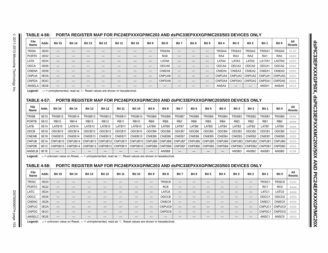
2
01
1-2
01
3 M
icroch
ip T
ech
no
log
y Inc.
DS
70
00
06
57
H-p
ag
e 1
03
ds
PIC
33E
PX
XX
GP
50X
, ds
PIC
33E
PX
XX
MC
20X
/50X
AN
D P
IC2
4EP
XX
XG
P/M
C2
0X
TA EVICES ONLY
TA EVICES ONLY
TA EVICES ONLY
NBit 3 Bit 2 Bit 1 Bit 0
All Resets
TR RISA3 TRISA2 TRISA1 TRISA0 011F
PO RA3 RA2 RA1 RA0 0000
LA LATA3 LATA2 LA1TA1 LA0TA0 0000
OD DCA3 ODCA2 ODCA1 ODCA0 0000
CN NIEA3 CNIEA2 CNIEA1 CNIEA0 0000
CN NPUA3 CNPUA2 CNPUA1 CNPUA0 0000
CN NPDA3 CNPDA2 CNPDA1 CNPDA0 0000
AN — — ANSA1 ANSA0 0013
Le
NBit 3 Bit 2 Bit 1 Bit 0
All Resets
TR TRISB3 TRISB2 TRISB1 TRISB0 FFFF
PO RB3 RB2 RB1 RB0 xxxx
LA LATB3 LATB2 LATB1 LATB0 xxxx
OD ODCB3 ODCB2 ODCB1 ODCB0 0000
CN CNIEB3 CNIEB2 CNIEB1 CNIEB0 0000
CN NPUB3 CNPUB2 CNPUB1 CNPUB0 0000
CN NPDB3 CNPDB2 CNPDB1 CNPDB0 0000
AN ANSB3 ANSB2 ANSB1 ANSB0 010F
Le
NBit 3 Bit 2 Bit 1 Bit 0
All Resets
TR — — TRISC1 TRISC0 0103
PO — — RC1 RC0 xxxx
LA — — LATC1 LATC0 xxxx
OD — — ODCC1 ODCC0 0000
CN — — CNIEC1 CNIEC0 0000
CN — — CNPUC1 CNPUC0 0000
CN — — CNPDC1 CNPDC0 0000
AN — — ANSC1 ANSC0 0003
Le
BLE 4-56: PORTA REGISTER MAP FOR PIC24EPXXXGP/MC203 AND dsPIC33EPXXXGP/MC203/503 D
BLE 4-57: PORTB REGISTER MAP FOR PIC24EPXXXGP/MC203 AND dsPIC33EPXXXGP/MC203/503 D
BLE 4-58: PORTC REGISTER MAP FOR PIC24EPXXXGP/MC203 AND dsPIC33EPXXXGP/MC203/503 D
File ame
Addr. Bit 15 Bit 14 Bit 13 Bit 12 Bit 11 Bit 10 Bit 9 Bit 8 Bit 7 Bit 6 Bit 5 Bit 4
ISA 0E00 — — — — — — — TRISA8 — — — TRISA4 T
RTA 0E02 — — — — — — — RA8 — — — RA4
TA 0E04 — — — — — — — LATA8 — — — LATA4
CA 0E06 — — — — — — — ODCA8 — — — ODCA4 O
ENA 0E08 — — — — — — — CNIEA8 — — — CNIEA4 C
PUA 0E0A — — — — — — — CNPUA8 — — — CNPUA4 C
PDA 0E0C — — — — — — — CNPDA8 — — — CNPDA4 C
SELA 0E0E — — — — — — — — — — — ANSA4
gend: — = unimplemented, read as ‘0’. Reset values are shown in hexadecimal.
File ame
Addr. Bit 15 Bit 14 Bit 13 Bit 12 Bit 11 Bit 10 Bit 9 Bit 8 Bit 7 Bit 6 Bit 5 Bit 4
ISB 0E10 TRISB15 TRISB14 TRISB13 TRISB12 TRISB11 TRISB10 TRISB9 TRISB8 TRISB7 TRISB6 TRISB5 TRISB4
RTB 0E12 RB15 RB14 RB13 RB12 RB11 RB10 RB9 RB8 RB7 RB6 RB5 RB4
TB 0E14 LATB15 LATB14 LATB13 LATB12 LATB11 LATB10 LATB9 LATB8 LATB7 LATB6 LATB5 LATB4
CB 0E16 ODCB15 ODCB14 ODCB13 ODCB12 ODCB11 ODCB10 ODCB9 ODCB8 ODCB7 ODCB6 ODCB5 ODCB4
ENB 0E18 CNIEB15 CNIEB14 CNIEB13 CNIEB12 CNIEB11 CNIEB10 CNIEB9 CNIEB8 CNIEB7 CNIEB6 CNIEB5 CNIEB4
PUB 0E1A CNPUB15 CNPUB14 CNPUB13 CNPUB12 CNPUB11 CNPUB10 CNPUB9 CNPUB8 CNPUB7 CNPUB6 CNPUB5 CNPUB4 C
PDB 0E1C CNPDB15 CNPDB14 CNPDB13 CNPDB12 CNPDB11 CNPDB10 CNPDB9 CNPDB8 CNPDB7 CNPDB6 CNPDB5 CNPDB4 C
SELB 0E1E — — — — — — — ANSB8 — — — —
gend: x = unknown value on Reset, — = unimplemented, read as ‘0’. Reset values are shown in hexadecimal.
File ame
Addr. Bit 15 Bit 14 Bit 13 Bit 12 Bit 11 Bit 10 Bit 9 Bit 8 Bit 7 Bit 6 Bit 5 Bit 4
ISC 0E20 — — — — — — — TRISC8 — — — —
RTC 0E22 — — — — — — — RC8 — — — —
TC 0E24 — — — — — — — LATC8 — — — —
CC 0E26 — — — — — — — ODCC8 — — — —
ENC 0E28 — — — — — — — CNIEC8 — — — —
PUC 0E2A — — — — — — — CNPUC8 — — — —
PDC 0E2C — — — — — — — CNPDC8 — — — —
SELC 0E2E — — — — — — — — — — — —
gend: x = unknown value on Reset, — = unimplemented, read as ‘0’. Reset values are shown in hexadecimal.

ds
PIC
33E
PX
XX
GP
50X
, dsP
IC33
EP
XX
XM
C20
X/5
0X A
ND
PIC
24E
PX
XX
GP
/MC
20X
DS
70
00
06
57
H-p
ag
e 1
04
2
01
1-2
01
3 M
icroch
ip T
ech
no
log
y Inc.
02 DEVICES ONLY
02 DEVICES ONLY
Bit 3 Bit 2 Bit 1 Bit 0All
Resets
4 TRISA3 TRISA2 TRISA1 TRISA0 001F
RA3 RA2 RA1 RA0 0000
4 LATA3 LATA2 LA1TA1 LA0TA0 0000
4 ODCA3 ODCA2 ODCA1 ODCA0 0000
4 CNIEA3 CNIEA2 CNIEA1 CNIEA0 0000
A4 CNPUA3 CNPUA2 CNPUA1 CNPUA0 0000
A4 CNPDA3 CNPDA2 CNPDA1 CNPDA0 0000
4 — — ANSA1 ANSA0 0013
4 Bit 3 Bit 2 Bit 1 Bit 0All
Resets
B4 TRISB3 TRISB2 TRISB1 TRISB0 FFFF
4 RB3 RB2 RB1 RB0 xxxx
4 LATB3 LATB2 LATB1 LATB0 xxxx
B4 ODCB3 ODCB2 ODCB1 ODCB0 0000
B4 CNIEB3 CNIEB2 CNIEB1 CNIEB0 0000
B4 CNPUB3 CNPUB2 CNPUB1 CNPUB0 0000
B4 CNPDB3 CNPDB2 CNPDB1 CNPDB0 0000
ANSB3 ANSB2 ANSB1 ANSB0 010F
TABLE 4-59: PORTA REGISTER MAP FOR PIC24EPXXXGP/MC202 AND dsPIC33EPXXXGP/MC202/5
TABLE 4-60: PORTB REGISTER MAP FOR PIC24EPXXXGP/MC202 AND dsPIC33EPXXXGP/MC202/5
File Name
Addr. Bit 15 Bit 14 Bit 13 Bit 12 Bit 11 Bit 10 Bit 9 Bit 8 Bit 7 Bit 6 Bit 5 Bit 4
TRISA 0E00 — — — — — — — — — — — TRISA
PORTA 0E02 — — — — — — — — — — — RA4
LATA 0E04 — — — — — — — — — — — LATA
ODCA 0E06 — — — — — — — — — — — ODCA
CNENA 0E08 — — — — — — — — — — — CNIEA
CNPUA 0E0A — — — — — — — — — — — CNPU
CNPDA 0E0C — — — — — — — — — — — CNPD
ANSELA 0E0E — — — — — — — — — — — ANSA
Legend: — = unimplemented, read as ‘0’. Reset values are shown in hexadecimal.
File Name
Addr. Bit 15 Bit 14 Bit 13 Bit 12 Bit 11 Bit 10 Bit 9 Bit 8 Bit 7 Bit 6 Bit 5 Bit
TRISB 0E10 TRISB15 TRISB14 TRISB13 TRISB12 TRISB11 TRISB10 TRISB9 TRISB8 TRISB7 TRISB6 TRISB5 TRIS
PORTB 0E12 RB15 RB14 RB13 RB12 RB11 RB10 RB9 RB8 RB7 RB6 RB5 RB
LATB 0E14 LATB15 LATB14 LATB13 LATB12 LATB11 LATB10 LATB9 LATB8 LATB7 LATB6 LATB5 LATB
ODCB 0E16 ODCB15 ODCB14 ODCB13 ODCB12 ODCB11 ODCB10 ODCB9 ODCB8 ODCB7 ODCB6 ODCB5 ODC
CNENB 0E18 CNIEB15 CNIEB14 CNIEB13 CNIEB12 CNIEB11 CNIEB10 CNIEB9 CNIEB8 CNIEB7 CNIEB6 CNIEB5 CNIE
CNPUB 0E1A CNPUB15 CNPUB14 CNPUB13 CNPUB12 CNPUB11 CNPUB10 CNPUB9 CNPUB8 CNPUB7 CNPUB6 CNPUB5 CNPU
CNPDB 0E1C CNPDB15 CNPDB14 CNPDB13 CNPDB12 CNPDB11 CNPDB10 CNPDB9 CNPDB8 CNPDB7 CNPDB6 CNPDB5 CNPD
ANSELB 0E1E — — — — — — — ANSB8 — — — —
Legend: x = unknown value on Reset, — = unimplemented, read as ‘0’. Reset values are shown in hexadecimal.

dsPIC33EPXXXGP50X, dsPIC33EPXXXMC20X/50X AND PIC24EPXXXGP/MC20X
4.4.1 PAGED MEMORY SCHEME
The dsPIC33EPXXXGP50X, dsPIC33EPXXXMC20X/50X and PIC24EPXXXGP/MC20X architectureextends the available Data Space through a pagingscheme, which allows the available Data Space tobe accessed using MOV instructions in a linearfashion for pre-modified and post-modified EffectiveAddresses (EA). The upper half of the base DataSpace address is used in conjunction with the DataSpace Page registers, the 10-bit Read Page register(DSRPAG) or the 9-bit Write Page register(DSWPAG), to form an Extended Data Space (EDS)
address or Program Space Visibility (PSV) address.The Data Space Page registers are located in theSFR space.
Construction of the EDS address is shown inExample 4-1. When DSRPAG<9> = 0 and the baseaddress bit, EA<15> = 1, the DSRPAG<8:0> bits areconcatenated onto EA<14:0> to form the 24-bit EDSread address. Similarly, when base address bit,EA<15> = 1, DSWPAG<8:0> are concatenated ontoEA<14:0> to form the 24-bit EDS write address.
EXAMPLE 4-1: EXTENDED DATA SPACE (EDS) READ ADDRESS GENERATION
1
DSRPAG<8:0>
9 Bits
EA
15 Bits
Select
Byte24-Bit EDS EASelect
EA(DSRPAG = Don’t care)
No EDS Access
Select16-Bit DS EAByte
EA<15> = 0
DSRPAG
0
EA<15>
Note: DS read access when DSRPAG = 0x000 will force an address error trap.
= 1?DSRPAG<9>
Y
N
GeneratePSV Address
0
2011-2013 Microchip Technology Inc. DS70000657H-page 105

dsPIC33EPXXXGP50X, dsPIC33EPXXXMC20X/50X AND PIC24EPXXXGP/MC20X
EXAMPLE 4-2: EXTENDED DATA SPACE (EDS) WRITE ADDRESS GENERATION
The paged memory scheme provides access tomultiple 32-Kbyte windows in the EDS and PSVmemory. The Data Space Page registers, DSxPAG, incombination with the upper half of the Data Spaceaddress, can provide up to 16 Mbytes of additionaladdress space in the EDS and 8 Mbytes (DSRPAGonly) of PSV address space. The paged data memoryspace is shown in Example 4-3.
The Program Space (PS) can be accessed with aDSRPAG of 0x200 or greater. Only reads from PS aresupported using the DSRPAG. Writes to PS are notsupported, so DSWPAG is dedicated to DS, includingEDS only. The Data Space and EDS can be read from,and written to, using DSRPAG and DSWPAG,respectively.
1
DSWPAG<8:0>
9 Bits
EA
15 Bits
Byte24-Bit EDS EASelect
EA
(DSWPAG = don’t care)
No EDS Access
Select16-Bit DS EAByte
EA<15> = 0
EA<15>
Note: DS read access when DSRPAG = 0x000 will force an address error trap.
GeneratePSV Address
0
DS70000657H-page 106 2011-2013 Microchip Technology Inc.

2
01
1-2
01
3 M
icroch
ip T
ech
no
log
y Inc.
DS
70
00
06
57
H-p
ag
e 1
07
ds
PIC
33E
PX
XX
GP
50X
, ds
PIC
33E
PX
XX
MC
20X
/50X
AN
D P
IC2
4EP
XX
XG
P/M
C2
0X
EXTable Address Space
(TBLPAG<7:0>)
0x0000(TBLPAG = 0x00)
0xFFFF
S_Addr<15:0>
lsw UsingTBLRDL/TBLWTL
MSB UsingTBLRDH/TBLWTH
0x0000(TBLPAG = 0x7F)
0xFFFF
lsw UsingTBLRDL/TBLWTL
MSB UsingTBLRDH/TBLWTH
re information.
AMPLE 4-3: PAGED DATA MEMORY SPACE
0x0000
Program Memory0x0000
0x7FFF
0x7FFF
EDS Page 0x001
0x0000SFR Registers
0x0FFF0x1000
Up to 8-Kbyte
0x2FFF
Local Data Space EDS(DSRPAG<9:0>/DSWPAG<8:0>)
Reserved(Will produce an
address error trap)
32-KbyteEDS Window
0xFFFF
0x3000
Page 0
Program Space
0x00_0000
0x7F_FFFF
(lsw – <15:0>)
0x0000
(DSRPAG = 0x001)(DSWPAG = 0x001)
EDS Page 0x1FF(DSRPAG = 0x1FF)(DSWPAG = 0x1FF)
EDS Page 0x200(DSRPAG = 0x200)
PSVProgramMemory
EDS Page 0x2FF(DSRPAG = 0x2FF)
EDS Page 0x300(DSRPAG = 0x300)
EDS Page 0x3FF(DSRPAG = 0x3FF)
0x7FFF
0x0000
0x7FFF
0x0000
0x7FFF0x0000
0x7FFF
0x0000
0x7FFF
DS_Addr<14:0>
DS_Addr<15:0>
(lsw)
PSVProgramMemory(MSB)
Program Memory
0x00_0000
0x7F_FFFF
(MSB – <23:16>)
D
(Instruction & Data)
No writes allowed
No writes allowed
No writes allowed
No writes allowed
RAM(1)
0x7FFF0x8000
Note 1: For 64K Flash devices. RAM size and end location is dependent on device; see Section 4.2 “Data Address Space” for mo

dsPIC33EPXXXGP50X, dsPIC33EPXXXMC20X/50X AND PIC24EPXXXGP/MC20X
Allocating different Page registers for read and writeaccess allows the architecture to support datamovement between different pages in data memory.This is accomplished by setting the DSRPAG registervalue to the page from which you want to read, andconfiguring the DSWPAG register to the page to whichit needs to be written. Data can also be moved fromdifferent PSV to EDS pages, by configuring theDSRPAG and DSWPAG registers to address PSV andEDS space, respectively. The data can be movedbetween pages by a single instruction.
When an EDS or PSV page overflow or underflowoccurs, EA<15> is cleared as a result of the registerindirect EA calculation. An overflow or underflow of theEA in the EDS or PSV pages can occur at the pageboundaries when:
• The initial address prior to modification addresses an EDS or PSV page
• The EA calculation uses Pre-Modified or Post-Modified Register Indirect Addressing; however, this does not include Register Offset Addressing
In general, when an overflow is detected, the DSxPAGregister is incremented and the EA<15> bit is set tokeep the base address within the EDS or PSV window.When an underflow is detected, the DSxPAG register isdecremented and the EA<15> bit is set to keep thebase address within the EDS or PSV window. Thiscreates a linear EDS and PSV address space, but onlywhen using Register Indirect Addressing modes.
Exceptions to the operation described above arisewhen entering and exiting the boundaries of Page 0,EDS and PSV spaces. Table 4-61 lists the effects ofoverflow and underflow scenarios at differentboundaries.
In the following cases, when overflow or underflowoccurs, the EA<15> bit is set and the DSxPAG is notmodified; therefore, the EA will wrap to the beginning ofthe current page:
• Register Indirect with Register Offset Addressing
• Modulo Addressing
• Bit-Reversed Addressing
TABLE 4-61: OVERFLOW AND UNDERFLOW SCENARIOS AT PAGE 0, EDS and PSV SPACE BOUNDARIES(2,3,4)
O/U, R/W
Operation
Before After
DSxPAGDS
EA<15>Page
DescriptionDSxPAG
DSEA<15>
Page Description
O,Read
[++Wn]or
[Wn++]
DSRPAG = 0x1FF 1 EDS: Last page DSRPAG = 0x1FF 0 See Note 1
O,Read
DSRPAG = 0x2FF 1 PSV: Last lsw page
DSRPAG = 0x300 1 PSV: First MSB page
O,Read
DSRPAG = 0x3FF 1 PSV: Last MSB page
DSRPAG = 0x3FF 0 See Note 1
O,Write
DSWPAG = 0x1FF 1 EDS: Last page DSWPAG = 0x1FF 0 See Note 1
U,Read
[--Wn]or
[Wn--]
DSRPAG = 0x001 1 PSV page DSRPAG = 0x001 0 See Note 1
U,Read
DSRPAG = 0x200 1 PSV: First lsw page
DSRPAG = 0x200 0 See Note 1
U,Read
DSRPAG = 0x300 1 PSV: First MSB page
DSRPAG = 0x2FF 1 PSV: Last lsw page
Legend: O = Overflow, U = Underflow, R = Read, W = Write
Note 1: The Register Indirect Addressing now addresses a location in the base Data Space (0x0000-0x8000).
2: An EDS access with DSxPAG = 0x000 will generate an address error trap.
3: Only reads from PS are supported using DSRPAG. An attempt to write to PS using DSWPAG will generate an address error trap.
4: Pseudo-Linear Addressing is not supported for large offsets.
DS70000657H-page 108 2011-2013 Microchip Technology Inc.
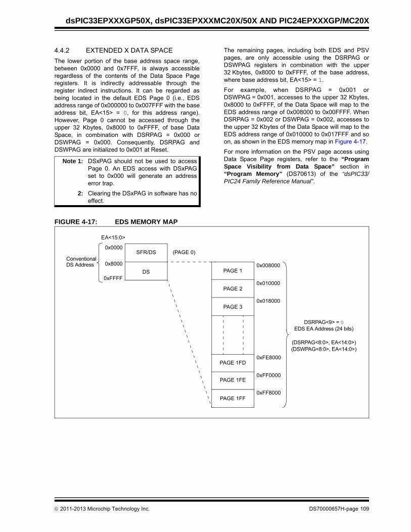
dsPIC33EPXXXGP50X, dsPIC33EPXXXMC20X/50X AND PIC24EPXXXGP/MC20X
4.4.2 EXTENDED X DATA SPACE
The lower portion of the base address space range,between 0x0000 and 0x7FFF, is always accessibleregardless of the contents of the Data Space Pageregisters. It is indirectly addressable through theregister indirect instructions. It can be regarded asbeing located in the default EDS Page 0 (i.e., EDSaddress range of 0x000000 to 0x007FFF with the baseaddress bit, EA<15> = 0, for this address range).However, Page 0 cannot be accessed through theupper 32 Kbytes, 0x8000 to 0xFFFF, of base DataSpace, in combination with DSRPAG = 0x000 orDSWPAG = 0x000. Consequently, DSRPAG andDSWPAG are initialized to 0x001 at Reset.
The remaining pages, including both EDS and PSVpages, are only accessible using the DSRPAG orDSWPAG registers in combination with the upper32 Kbytes, 0x8000 to 0xFFFF, of the base address,where base address bit, EA<15> = 1.
For example, when DSRPAG = 0x001 orDSWPAG = 0x001, accesses to the upper 32 Kbytes,0x8000 to 0xFFFF, of the Data Space will map to theEDS address range of 0x008000 to 0x00FFFF. WhenDSRPAG = 0x002 or DSWPAG = 0x002, accesses tothe upper 32 Kbytes of the Data Space will map to theEDS address range of 0x010000 to 0x017FFF and soon, as shown in the EDS memory map in Figure 4-17.
For more information on the PSV page access usingData Space Page registers, refer to the “ProgramSpace Visibility from Data Space” section in“Program Memory” (DS70613) of the “dsPIC33/PIC24 Family Reference Manual”.
FIGURE 4-17: EDS MEMORY MAP
Note 1: DSxPAG should not be used to accessPage 0. An EDS access with DSxPAGset to 0x000 will generate an addresserror trap.
2: Clearing the DSxPAG in software has noeffect.
0x008000
0x010000
0x018000PAGE 3
PAGE 2
PAGE 1FD0xFE8000
0xFF0000
0xFF8000PAGE 1FF
PAGE 1FE
SFR/DS0x0000
0xFFFF
EDS EA Address (24 bits)
DS
Conventional
EA<15:0>
0x8000
(PAGE 0)
(DSRPAG<8:0>, EA<14:0>)(DSWPAG<8:0>, EA<14:0>)
PAGE 1
DSRPAG<9> = 0
DS Address
2011-2013 Microchip Technology Inc. DS70000657H-page 109

dsPIC33EPXXXGP50X, dsPIC33EPXXXMC20X/50X AND PIC24EPXXXGP/MC20X
4.4.3 DATA MEMORY ARBITRATION AND BUS MASTER PRIORITY
EDS accesses from bus masters in the system arearbitrated.
The arbiter for data memory (including EDS) arbitratesbetween the CPU, the DMA and the ICD module. In theevent of coincidental access to a bus by the busmasters, the arbiter determines which bus masteraccess has the highest priority. The other bus mastersare suspended and processed after the access of thebus by the bus master with the highest priority.
By default, the CPU is Bus Master 0 (M0) with thehighest priority and the ICD is Bus Master 4 (M4) withthe lowest priority. The remaining bus master (DMAController) is allocated to M3 (M1 and M2 are reservedand cannot be used). The user application may raise orlower the priority of the DMA Controller to be above thatof the CPU by setting the appropriate bits in the EDSBus Master Priority Control (MSTRPR) register. All busmasters with raised priorities will maintain the samepriority relationship relative to each other (i.e., M1being highest and M3 being lowest, with M2 inbetween). Also, all the bus masters with priorities below
that of the CPU maintain the same priority relationshiprelative to each other. The priority schemes for busmasters with different MSTRPR values are tabulated inTable 4-62.
This bus master priority control allows the userapplication to manipulate the real-time response of thesystem, either statically during initialization ordynamically in response to real-time events.
TABLE 4-62: DATA MEMORY BUS ARBITER PRIORITY
FIGURE 4-18: ARBITER ARCHITECTURE
PriorityMSTRPR<15:0> Bit Setting(1)
0x0000 0x0020
M0 (highest) CPU DMA
M1 Reserved CPU
M2 Reserved Reserved
M3 DMA Reserved
M4 (lowest) ICD ICD
Note 1: All other values of MSTRPR<15:0> are reserved.
ICDReserved
Data Memory Arbiter
M0 M1 M2 M3 M4
MSTRPR<15:0>
DMA CPU
SRAM
DS70000657H-page 110 2011-2013 Microchip Technology Inc.

dsPIC33EPXXXGP50X, dsPIC33EPXXXMC20X/50X AND PIC24EPXXXGP/MC20X
4.4.4 SOFTWARE STACK
The W15 register serves as a dedicated SoftwareStack Pointer (SSP) and is automatically modified byexception processing, subroutine calls and returns;however, W15 can be referenced by any instruction inthe same manner as all other W registers. Thissimplifies reading, writing and manipulating of theStack Pointer (for example, creating stack frames).
W15 is initialized to 0x1000 during all Resets. Thisaddress ensures that the SSP points to valid RAM in alldsPIC33EPXXXGP50X, dsPIC33EPXXXMC20X/50Xand PIC24EPXXXGP/MC20X devices, and permitsstack availability for non-maskable trap exceptions.These can occur before the SSP is initialized by the usersoftware. You can reprogram the SSP duringinitialization to any location within Data Space.
The Software Stack Pointer always points to the firstavailable free word and fills the software stackworking from lower toward higher addresses.Figure 4-19 illustrates how it pre-decrements for astack pop (read) and post-increments for a stack push(writes).
When the PC is pushed onto the stack, PC<15:0> arepushed onto the first available stack word, thenPC<22:16> are pushed into the second available stacklocation. For a PC push during any CALL instruction,the MSB of the PC is zero-extended before the push,as shown in Figure 4-19. During exception processing,the MSB of the PC is concatenated with the lower 8 bitsof the CPU STATUS Register, SR. This allows thecontents of SRL to be preserved automatically duringinterrupt processing.
FIGURE 4-19: CALL STACK FRAME
Note: To protect against misaligned stackaccesses, W15<0> is fixed to ‘0’ by thehardware.
Note 1: To maintain system Stack Pointer (W15)coherency, W15 is never subject to(EDS) paging, and is therefore restrictedto an address range of 0x0000 to0xFFFF. The same applies to the W14when used as a Stack Frame Pointer(SFA = 1).
2: As the stack can be placed in, and canaccess X and Y spaces, care must betaken regarding its use, particularly withregard to local automatic variables in a Cdevelopment environment
<Free Word>
PC<15:0>
b‘000000000’
015
W15 (before CALL)
W15 (after CALL)S
tack
Gro
ws
Tow
ard
Hig
he
r A
ddre
ss
0x0000
PC<22:16>
CALL SUBR
2011-2013 Microchip Technology Inc. DS70000657H-page 111

dsPIC33EPXXXGP50X, dsPIC33EPXXXMC20X/50X AND PIC24EPXXXGP/MC20X
4.5 Instruction Addressing Modes
The addressing modes shown in Table 4-63 form thebasis of the addressing modes optimized to support thespecific features of individual instructions. Theaddressing modes provided in the MAC class ofinstructions differ from those in the other instructiontypes.
4.5.1 FILE REGISTER INSTRUCTIONS
Most file register instructions use a 13-bit address field(f) to directly address data present in the first8192 bytes of data memory (Near Data Space). Mostfile register instructions employ a working register, W0,which is denoted as WREG in these instructions. Thedestination is typically either the same file register orWREG (with the exception of the MUL instruction),which writes the result to a register or register pair. TheMOV instruction allows additional flexibility and canaccess the entire Data Space.
4.5.2 MCU INSTRUCTIONS
The three-operand MCU instructions are of the form:
Operand 3 = Operand 1 <function> Operand 2
where Operand 1 is always a working register (that is,the addressing mode can only be Register Direct),which is referred to as Wb. Operand 2 can be a W reg-ister fetched from data memory or a 5-bit literal. Theresult location can either be a W register or a datamemory location. The following addressing modes aresupported by MCU instructions:
• Register Direct
• Register Indirect
• Register Indirect Post-Modified
• Register Indirect Pre-Modified
• 5-Bit or 10-Bit Literal
TABLE 4-63: FUNDAMENTAL ADDRESSING MODES SUPPORTED
Note: Not all instructions support all theaddressing modes given above. Individ-ual instructions can support differentsubsets of these addressing modes.
Addressing Mode Description
File Register Direct The address of the file register is specified explicitly.
Register Direct The contents of a register are accessed directly.
Register Indirect The contents of Wn form the Effective Address (EA).
Register Indirect Post-Modified The contents of Wn form the EA. Wn is post-modified (incremented or decremented) by a constant value.
Register Indirect Pre-Modified Wn is pre-modified (incremented or decremented) by a signed constant value to form the EA.
Register Indirect with Register Offset (Register Indexed)
The sum of Wn and Wb forms the EA.
Register Indirect with Literal Offset The sum of Wn and a literal forms the EA.
DS70000657H-page 112 2011-2013 Microchip Technology Inc.
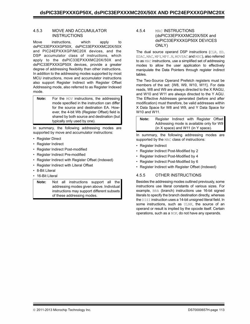
dsPIC33EPXXXGP50X, dsPIC33EPXXXMC20X/50X AND PIC24EPXXXGP/MC20X
4.5.3 MOVE AND ACCUMULATOR INSTRUCTIONS
Move instructions, which apply todsPIC33EPXXXGP50X, dsPIC33EPXXXMC20X/50Xand PIC24EPXXXGP/MC20X devices, and theDSP accumulator class of instructions, whichapply to the dsPIC33EPXXXMC20X/50X anddsPIC33EPXXXGP50X devices, provide a greaterdegree of addressing flexibility than other instructions.In addition to the addressing modes supported by mostMCU instructions, move and accumulator instructionsalso support Register Indirect with Register OffsetAddressing mode, also referred to as Register Indexedmode.
In summary, the following addressing modes aresupported by move and accumulator instructions:
• Register Direct
• Register Indirect
• Register Indirect Post-modified
• Register Indirect Pre-modified
• Register Indirect with Register Offset (Indexed)
• Register Indirect with Literal Offset
• 8-Bit Literal
• 16-Bit Literal
4.5.4 MAC INSTRUCTIONS (dsPIC33EPXXXMC20X/50X and dsPIC33EPXXXGP50X DEVICES ONLY)
The dual source operand DSP instructions (CLR, ED,EDAC, MAC, MPY, MPY.N, MOVSAC and MSC), also referredto as MAC instructions, use a simplified set of addressingmodes to allow the user application to effectivelymanipulate the Data Pointers through register indirecttables.
The Two-Source Operand Prefetch registers must bemembers of the set: {W8, W9, W10, W11}. For datareads, W8 and W9 are always directed to the X RAGU,and W10 and W11 are always directed to the Y AGU.The Effective Addresses generated (before and aftermodification) must therefore, be valid addresses withinX Data Space for W8 and W9, and Y Data Space forW10 and W11.
In summary, the following addressing modes aresupported by the MAC class of instructions:
• Register Indirect
• Register Indirect Post-Modified by 2
• Register Indirect Post-Modified by 4
• Register Indirect Post-Modified by 6
• Register Indirect with Register Offset (Indexed)
4.5.5 OTHER INSTRUCTIONS
Besides the addressing modes outlined previously, someinstructions use literal constants of various sizes. Forexample, BRA (branch) instructions use 16-bit signedliterals to specify the branch destination directly, whereasthe DISI instruction uses a 14-bit unsigned literal field. Insome instructions, such as ULNK, the source of anoperand or result is implied by the opcode itself. Certainoperations, such as a NOP, do not have any operands.
Note: For the MOV instructions, the addressingmode specified in the instruction can differfor the source and destination EA. How-ever, the 4-bit Wb (Register Offset) field isshared by both source and destination (buttypically only used by one).
Note: Not all instructions support all theaddressing modes given above. Individualinstructions may support different subsetsof these addressing modes.
Note: Register Indirect with Register OffsetAddressing mode is available only for W9(in X space) and W11 (in Y space).
2011-2013 Microchip Technology Inc. DS70000657H-page 113

dsPIC33EPXXXGP50X, dsPIC33EPXXXMC20X/50X AND PIC24EPXXXGP/MC20X
4.6 Modulo Addressing (dsPIC33EPXXXMC20X/50X and dsPIC33EPXXXGP50X Devices Only)
Modulo Addressing mode is a method of providing anautomated means to support circular data buffers usinghardware. The objective is to remove the need forsoftware to perform data address boundary checkswhen executing tightly looped code, as is typical inmany DSP algorithms.
Modulo Addressing can operate in either Data or Pro-gram Space (since the Data Pointer mechanism isessentially the same for both). One circular buffer can besupported in each of the X (which also provides the point-ers into Program Space) and Y Data Spaces. ModuloAddressing can operate on any W Register Pointer. How-ever, it is not advisable to use W14 or W15 for ModuloAddressing since these two registers are used as theStack Frame Pointer and Stack Pointer, respectively.
In general, any particular circular buffer can be config-ured to operate in only one direction, as there are certainrestrictions on the buffer start address (for incrementingbuffers) or end address (for decrementing buffers),based upon the direction of the buffer.
The only exception to the usage restrictions is forbuffers that have a power-of-two length. As thesebuffers satisfy the start and end address criteria, theycan operate in a bidirectional mode (that is, addressboundary checks are performed on both the lower andupper address boundaries).
4.6.1 START AND END ADDRESS
The Modulo Addressing scheme requires that astarting and ending address be specified, and loadedinto the 16-bit Modulo Buffer Address registers:XMODSRT, XMODEND, YMODSRT and YMODEND(see Table 4-1).
The length of a circular buffer is not directly specified. Itis determined by the difference between the corre-sponding start and end addresses. The maximumpossible length of the circular buffer is 32K words(64 Kbytes).
4.6.2 W ADDRESS REGISTER SELECTION
The Modulo and Bit-Reversed Addressing Controlregister, MODCON<15:0>, contains enable flags as wellas a W register field to specify the W Address registers.The XWM and YWM fields select the registers thatoperate with Modulo Addressing:
• If XWM = 1111, X RAGU and X WAGU Modulo Addressing is disabled
• If YWM = 1111, Y AGU Modulo Addressing is disabled
The X Address Space Pointer W register (XWM), towhich Modulo Addressing is to be applied, is stored inMODCON<3:0> (see Table 4-1). Modulo Addressing isenabled for X Data Space when XWM is set to anyvalue other than ‘1111’ and the XMODEN bit is set(MODCON<15>).
The Y Address Space Pointer W register (YWM), towhich Modulo Addressing is to be applied, is stored inMODCON<7:4>. Modulo Addressing is enabled for YData Space when YWM is set to any value other than‘1111’ and the YMODEN bit is set at MODCON<14>.
FIGURE 4-20: MODULO ADDRESSING OPERATION EXAMPLE
Note: Y space Modulo Addressing EA calcula-tions assume word-sized data (LSb ofevery EA is always clear).
0x1100
0x1163
Start Addr = 0x1100End Addr = 0x1163Length = 50 words
ByteAddress
MOV #0x1100, W0MOV W0, XMODSRT ;set modulo start addressMOV #0x1163, W0MOV W0, MODEND ;set modulo end addressMOV #0x8001, W0MOV W0, MODCON ;enable W1, X AGU for modulo
MOV #0x0000, W0 ;W0 holds buffer fill value
MOV #0x1110, W1 ;point W1 to buffer
DO AGAIN, #0x31 ;fill the 50 buffer locationsMOV W0, [W1++] ;fill the next locationAGAIN: INC W0, W0 ;increment the fill value
DS70000657H-page 114 2011-2013 Microchip Technology Inc.

dsPIC33EPXXXGP50X, dsPIC33EPXXXMC20X/50X AND PIC24EPXXXGP/MC20X
4.6.3 MODULO ADDRESSING APPLICABILITY
Modulo Addressing can be applied to the EffectiveAddress (EA) calculation associated with any Wregister. Address boundaries check for addressesequal to:
• The upper boundary addresses for incrementing buffers
• The lower boundary addresses for decrementing buffers
It is important to realize that the address boundariescheck for addresses less than, or greater than, theupper (for incrementing buffers) and lower (fordecrementing buffers) boundary addresses (not justequal to). Address changes can, therefore, jumpbeyond boundaries and still be adjusted correctly.
4.7 Bit-Reversed Addressing(dsPIC33EPXXXMC20X/50X and dsPIC33EPXXXGP50X Devices Only)
Bit-Reversed Addressing mode is intended to simplifydata reordering for radix-2 FFT algorithms. It issupported by the X AGU for data writes only.
The modifier, which can be a constant value or registercontents, is regarded as having its bit order reversed.The address source and destination are kept in normalorder. Thus, the only operand requiring reversal is themodifier.
4.7.1 BIT-REVERSED ADDRESSING IMPLEMENTATION
Bit-Reversed Addressing mode is enabled when allthese conditions are met:
• BWMx bits (W register selection) in the MODCON register are any value other than ‘1111’ (the stack cannot be accessed using Bit-Reversed Addressing)
• The BREN bit is set in the XBREV register
• The addressing mode used is Register Indirect with Pre-Increment or Post-Increment
If the length of a bit-reversed buffer is M = 2N bytes,the last ‘N’ bits of the data buffer start address mustbe zeros.
XBREV<14:0> is the Bit-Reversed Addressing modi-fier, or ‘pivot point’, which is typically a constant. In thecase of an FFT computation, its value is equal to half ofthe FFT data buffer size.
When enabled, Bit-Reversed Addressing is executedonly for Register Indirect with Pre-Increment or Post-Increment Addressing and word-sized data writes. Itdoes not function for any other addressing mode or forbyte-sized data and normal addresses are generatedinstead. When Bit-Reversed Addressing is active, theW Address Pointer is always added to the addressmodifier (XBREVx) and the offset associated with theRegister Indirect Addressing mode is ignored. Inaddition, as word-sized data is a requirement, the LSbof the EA is ignored (and always clear).
If Bit-Reversed Addressing has already been enabledby setting the BREN (XBREV<15>) bit, a write to theXBREV register should not be immediately followed byan indirect read operation using the W register that hasbeen designated as the Bit-Reversed Pointer.
Note: The modulo corrected Effective Addressis written back to the register only whenPre-Modify or Post-Modify Addressingmode is used to compute the EffectiveAddress. When an address offset (suchas [W7 + W2]) is used, ModuloAddressing correction is performed butthe contents of the register remainunchanged.
Note: All bit-reversed EA calculations assumeword-sized data (LSb of every EA is alwaysclear). The XBREVx value is scaledaccordingly to generate compatible (byte)addresses.
Note: Modulo Addressing and Bit-ReversedAddressing can be enabled simultaneouslyusing the same W register, but Bit-Reversed Addressing operation will alwaystake precedence for data writes whenenabled.
2011-2013 Microchip Technology Inc. DS70000657H-page 115

dsPIC33EPXXXGP50X, dsPIC33EPXXXMC20X/50X AND PIC24EPXXXGP/MC20X
FIGURE 4-21: BIT-REVERSED ADDRESSING EXAMPLE
TABLE 4-64: BIT-REVERSED ADDRESSING SEQUENCE (16-ENTRY)
Normal Address Bit-Reversed Address
A3 A2 A1 A0 Decimal A3 A2 A1 A0 Decimal
0 0 0 0 0 0 0 0 0 0
0 0 0 1 1 1 0 0 0 8
0 0 1 0 2 0 1 0 0 4
0 0 1 1 3 1 1 0 0 12
0 1 0 0 4 0 0 1 0 2
0 1 0 1 5 1 0 1 0 10
0 1 1 0 6 0 1 1 0 6
0 1 1 1 7 1 1 1 0 14
1 0 0 0 8 0 0 0 1 1
1 0 0 1 9 1 0 0 1 9
1 0 1 0 10 0 1 0 1 5
1 0 1 1 11 1 1 0 1 13
1 1 0 0 12 0 0 1 1 3
1 1 0 1 13 1 0 1 1 11
1 1 1 0 14 0 1 1 1 7
1 1 1 1 15 1 1 1 1 15
b3 b2 b1 0
b2 b3 b4 0
Bit Locations Swapped Left-to-RightAround Center of Binary Value
Bit-Reversed Address
XBREV<14:0> = 0x0008 for a 16-Word Bit-Reversed Buffer
b7 b6 b5 b1
b7 b6 b5 b4b11 b10 b9 b8
b11 b10 b9 b8
b15 b14 b13 b12
b15 b14 b13 b12
Sequential Address
Pivot Point
DS70000657H-page 116 2011-2013 Microchip Technology Inc.

dsPIC33EPXXXGP50X, dsPIC33EPXXXMC20X/50X AND PIC24EPXXXGP/MC20X
4.8 Interfacing Program and Data Memory Spaces
The dsPIC33EPXXXGP50X, dsPIC33EPXXXMC20X/50X and PIC24EPXXXGP/MC20X architecture uses a24-bit-wide Program Space (PS) and a 16-bit-wideData Space (DS). The architecture is also a modifiedHarvard scheme, meaning that data can also bepresent in the Program Space. To use this data suc-cessfully, it must be accessed in a way that preservesthe alignment of information in both spaces.
Aside from normal execution, the architecture of thedsPIC33EPXXXGP50X, dsPIC33EPXXXMC20X/50Xand PIC24EPXXXGP/MC20X devices provides twomethods by which Program Space can be accessedduring operation:
• Using table instructions to access individual bytes or words anywhere in the Program Space
• Remapping a portion of the Program Space into the Data Space (Program Space Visibility)
Table instructions allow an application to read or writeto small areas of the program memory. This capabilitymakes the method ideal for accessing data tables thatneed to be updated periodically. It also allows accessto all bytes of the program word. The remappingmethod allows an application to access a large block ofdata on a read-only basis, which is ideal for look-upsfrom a large table of static data. The application canonly access the least significant word of the programword.
TABLE 4-65: PROGRAM SPACE ADDRESS CONSTRUCTION
FIGURE 4-22: DATA ACCESS FROM PROGRAM SPACE ADDRESS GENERATION
Access TypeAccessSpace
Program Space Address
<23> <22:16> <15> <14:1> <0>
Instruction Access(Code Execution)
User 0 PC<22:1> 0
0xx xxxx xxxx xxxx xxxx xxx0
TBLRD/TBLWT(Byte/Word Read/Write)
User TBLPAG<7:0> Data EA<15:0>
0xxx xxxx xxxx xxxx xxxx xxxx
Configuration TBLPAG<7:0> Data EA<15:0>
1xxx xxxx xxxx xxxx xxxx xxxx
0Program Counter
23 Bits
Program Counter(1)
TBLPAG
8 Bits
EA
16 Bits
Byte Select
0
1/0
User/Configuration
Table Operations(2)
Space Select
24 Bits
1/0
Note 1: The Least Significant bit (LSb) of Program Space addresses is always fixed as ‘0’ to maintain word alignment of data in the Program and Data Spaces.
2: Table operations are not required to be word-aligned. Table Read operations are permitted in the configuration memory space.
2011-2013 Microchip Technology Inc. DS70000657H-page 117

dsPIC33EPXXXGP50X, dsPIC33EPXXXMC20X/50X AND PIC24EPXXXGP/MC20X
4.8.1 DATA ACCESS FROM PROGRAM MEMORY USING TABLE INSTRUCTIONS
The TBLRDL and TBLWTL instructions offer a directmethod of reading or writing the lower word of anyaddress within the Program Space without goingthrough Data Space. The TBLRDH and TBLWTHinstructions are the only method to read or write theupper 8 bits of a Program Space word as data.
The PC is incremented by two for each successive 24-bitprogram word. This allows program memory addressesto directly map to Data Space addresses. Program mem-ory can thus be regarded as two 16-bit-wide wordaddress spaces, residing side by side, each with thesame address range. TBLRDL and TBLWTL access thespace that contains the least significant data word.TBLRDH and TBLWTH access the space that contains theupper data byte.
Two table instructions are provided to move byte orword-sized (16-bit) data to and from Program Space.Both function as either byte or word operations.
• TBLRDL (Table Read Low):
- In Word mode, this instruction maps the lower word of the Program Space location (P<15:0>) to a data address (D<15:0>)
- In Byte mode, either the upper or lower byte of the lower program word is mapped to the lower byte of a data address. The upper byte is selected when Byte Select is ‘1’; the lower byte is selected when it is ‘0’.
• TBLRDH (Table Read High):
- In Word mode, this instruction maps the entire upper word of a program address (P<23:16>) to a data address. The ‘phantom’ byte (D<15:8>) is always ‘0’.
- In Byte mode, this instruction maps the upper or lower byte of the program word to D<7:0> of the data address in the TBLRDL instruc-tion. The data is always ‘0’ when the upper ‘phantom’ byte is selected (Byte Select = 1).
In a similar fashion, two table instructions, TBLWTHand TBLWTL, are used to write individual bytes orwords to a Program Space address. The details oftheir operation are explained in Section 5.0 “FlashProgram Memory”.
For all table operations, the area of program memoryspace to be accessed is determined by the Table Pageregister (TBLPAG). TBLPAG covers the entire programmemory space of the device, including user applicationand configuration spaces. When TBLPAG<7> = 0, thetable page is located in the user memory space. WhenTBLPAG<7> = 1, the page is located in configurationspace.
FIGURE 4-23: ACCESSING PROGRAM MEMORY WITH TABLE INSTRUCTIONS
081623
0000000000000000
0000000000000000
‘Phantom’ Byte
TBLRDH.B (Wn<0> = 0)
TBLRDL.W
TBLRDL.B (Wn<0> = 1)
TBLRDL.B (Wn<0> = 0)
23 15 0
TBLPAG02
0x000000
0x800000
0x020000
0x030000
Program Space
The address for the table operation is determined by the data EAwithin the page defined by the TBLPAG register. Only read operations are shown; write operations are also valid inthe user memory area.
DS70000657H-page 118 2011-2013 Microchip Technology Inc.

dsPIC33EPXXXGP50X, dsPIC33EPXXXMC20X/50X AND PIC24EPXXXGP/MC20X
5.0 FLASH PROGRAM MEMORY
The dsPIC33EPXXXGP50X, dsPIC33EPXXXMC20X/50X and PIC24EPXXXGP/MC20X devices containinternal Flash program memory for storing andexecuting application code. The memory is readable,writable and erasable during normal operation over theentire VDD range.
Flash memory can be programmed in two ways:
• In-Circuit Serial Programming™ (ICSP™) programming capability
• Run-Time Self-Programming (RTSP)
ICSP allows for a dsPIC33EPXXXGP50X,dsPIC33EPXXXMC20X/50X and PIC24EPXXXGP/MC20X device to be serially programmed while in theend application circuit. This is done with two lines forprogramming clock and programming data (one of the
alternate programming pin pairs: PGECx/PGEDx), andthree other lines for power (VDD), ground (VSS) andMaster Clear (MCLR). This allows customers tomanufacture boards with unprogrammed devices andthen program the device just before shipping theproduct. This also allows the most recent firmware or acustom firmware to be programmed.
RTSP is accomplished using TBLRD (Table Read) andTBLWT (Table Write) instructions. With RTSP, the userapplication can write program memory data a singleprogram memory word, and erase program memory inblocks or ‘pages’ of 1024 instructions (3072 bytes) at atime.
5.1 Table Instructions and Flash Programming
Regardless of the method used, all programming ofFlash memory is done with the Table Read and TableWrite instructions. These allow direct read and writeaccess to the program memory space from the datamemory while the device is in normal operating mode.The 24-bit target address in the program memory isformed using bits<7:0> of the TBLPAG register and theEffective Address (EA) from a W register, specified inthe table instruction, as shown in Figure 5-1.
The TBLRDL and the TBLWTL instructions are used toread or write to bits<15:0> of program memory.TBLRDL and TBLWTL can access program memory inboth Word and Byte modes.
The TBLRDH and TBLWTH instructions are used to reador write to bits<23:16> of program memory. TBLRDHand TBLWTH can also access program memory in Wordor Byte mode.
FIGURE 5-1: ADDRESSING FOR TABLE REGISTERS
Note 1: This data sheet summarizes thefeatures of the dsPIC33EPXXXGP50X,dsPIC33EPXXXMC20X/50X andPIC24EPXXXGP/MC20X families ofdevices. It is not intended to be a compre-hensive reference source. To complementthe information in this data sheet, refer to“Flash Programming” (DS70609) inthe “dsPIC33/PIC24 Family ReferenceManual”, which is available from theMicrochip web site (www.microchip.com).
2: Some registers and associated bitsdescribed in this section may not beavailable on all devices. Refer toSection 4.0 “Memory Organization” inthis data sheet for device-specific registerand bit information.
0Program Counter
24 Bits
Program Counter
TBLPAG Reg
8 Bits
Working Reg EA
16 Bits
Byte24-Bit EA
0
1/0
Select
UsingTable Instruction
Using
User/ConfigurationSpace Select
2011-2013 Microchip Technology Inc. DS70000657H-page 119
dsPIC33EPXXXGP50X, dsPIC33EPXXXMC20X/50X AND PIC24EPXXXGP/MC20X
5.2 RTSP Operation
RTSP allows the user application to erase a singlepage of memory and to program two instruction wordsat a time. See the General Purpose and Motor ControlFamily tables (Table 1 and Table 2, respectively) for thepage sizes of each device.
For more information on erasing and programmingFlash memory, refer to “Flash Programming”(DS70609) in the “dsPIC33/PIC24 Family ReferenceManual”.
5.3 Programming Operations
A complete programming sequence is necessary forprogramming or erasing the internal Flash in RTSPmode. The processor stalls (waits) until the programmingoperation is finished.
For erase and program times, refer to Parameters D137aand D137b (Page Erase Time), and D138a andD138b (Word Write Cycle Time) in Table 30-14 inSection 30.0 “Electrical Characteristics”.
Setting the WR bit (NVMCON<15>) starts the opera-tion and the WR bit is automatically cleared when theoperation is finished.
5.3.1 PROGRAMMING ALGORITHM FOR FLASH PROGRAM MEMORY
Programmers can program two adjacent words(24 bits x 2) of program Flash memory at a time onevery other word address boundary (0x000002,0x000006, 0x00000A, etc.). To do this, it is necessaryto erase the page that contains the desired address ofthe location the user wants to change.
For protection against accidental operations, the writeinitiate sequence for NVMKEY must be used to allowany erase or program operation to proceed. After theprogramming command has been executed, the userapplication must wait for the programming time untilprogramming is complete. The two instructions follow-ing the start of the programming sequence should beNOPs.
Refer to Flash Programming” (DS70609) in the“dsPIC33/PIC24 Family Reference Manual” for detailsand codes examples on programming using RTSP.
5.4 Flash Memory Resources
Many useful resources are provided on the main prod-uct page of the Microchip web site for the devices listedin this data sheet. This product page, which can beaccessed using this link, contains the latest updatesand additional information.
5.4.1 KEY RESOURCES
• “Flash Programming” (DS70609) in the “dsPIC33/PIC24 Family Reference Manual”
• Code Samples
• Application Notes
• Software Libraries
• Webinars
• All Related “dsPIC33/PIC24 Family Reference Manual” Sections
• Development Tools
5.5 Control Registers
Four SFRs are used to erase and write the programFlash memory: NVMCON, NVMKEY, NVMADRH andNVMADRL.
The NVMCON register (Register 5-1) enables andinitiates Flash memory erase and write operations.
NVMKEY (Register 5-4) is a write-only register that isused for write protection. To start a programming orerase sequence, the user application mustconsecutively write 0x55 and 0xAA to the NVMKEYregister.
There are two NVM Address registers: NVMADRH andNVMADRL. These two registers, when concatenated,form the 24-bit Effective Address (EA) of the selectedword for programming operations or the selected pagefor erase operations.
The NVMADRH register is used to hold the upper 8 bitsof the EA, while the NVMADRL register is used to holdthe lower 16 bits of the EA.
Note: In the event you are not able to access theproduct page using the link above, enterthis URL in your browser:http://www.microchip.com/wwwproducts/Devices.aspx?dDocName=en555464
DS70000657H-page 120 2011-2013 Microchip Technology Inc.

dsPIC33EPXXXGP50X, dsPIC33EPXXXMC20X/50X AND PIC24EPXXXGP/MC20X
REGISTER 5-1: NVMCON: NONVOLATILE MEMORY (NVM) CONTROL REGISTER
R/SO-0(1) R/W-0(1) R/W-0(1) R/W-0 U-0 U-0 U-0 U-0
WR WREN WRERR NVMSIDL(2) — — — —
bit 15 bit 8
U-0 U-0 U-0 U-0 R/W-0(1) R/W-0(1) R/W-0(1) R/W-0(1)
— — — — NVMOP3(3,4) NVMOP2(3,4) NVMOP1(3,4) NVMOP0(3,4)
bit 7 bit 0
Legend: SO = Settable Only bit
R = Readable bit W = Writable bit U = Unimplemented bit, read as ‘0’
-n = Value at POR ‘1’ = Bit is set ‘0’ = Bit is cleared x = Bit is unknown
bit 15 WR: Write Control bit(1)
1 = Initiates a Flash memory program or erase operation; the operation is self-timed and the bit iscleared by hardware once the operation is complete
0 = Program or erase operation is complete and inactive
bit 14 WREN: Write Enable bit(1)
1 = Enables Flash program/erase operations0 = Inhibits Flash program/erase operations
bit 13 WRERR: Write Sequence Error Flag bit(1)
1 = An improper program or erase sequence attempt or termination has occurred (bit is set automaticallyon any set attempt of the WR bit)
0 = The program or erase operation completed normally
bit 12 NVMSIDL: NVM Stop in Idle Control bit(2)
1 = Flash voltage regulator goes into Standby mode during Idle mode0 = Flash voltage regulator is active during Idle mode
bit 11-4 Unimplemented: Read as ‘0’
bit 3-0 NVMOP<3:0>: NVM Operation Select bits(1,3,4)
1111 = Reserved1110 = Reserved1101 = Reserved1100 = Reserved1011 = Reserved1010 = Reserved0011 = Memory page erase operation0010 = Reserved0001 = Memory double-word program operation(5)
0000 = Reserved
Note 1: These bits can only be reset on a POR.
2: If this bit is set, there will be minimal power savings (IIDLE) and upon exiting Idle mode, there is a delay (TVREG) before Flash memory becomes operational.
3: All other combinations of NVMOP<3:0> are unimplemented.
4: Execution of the PWRSAV instruction is ignored while any of the NVM operations are in progress.
5: Two adjacent words on a 4-word boundary are programmed during execution of this operation.
2011-2013 Microchip Technology Inc. DS70000657H-page 121

dsPIC33EPXXXGP50X, dsPIC33EPXXXMC20X/50X AND PIC24EPXXXGP/MC20X
REGISTER 5-4: NVMKEY: NONVOLATILE MEMORY KEY
REGISTER 5-2: NVMADRH: NONVOLATILE MEMORY ADDRESS REGISTER HIGH
U-0 U-0 U-0 U-0 U-0 U-0 U-0 U-0
— — — — — — — —
bit 15 bit 8
R/W-x R/W-x R/W-x R/W-x R/W-x R/W-x R/W-x R/W-x
NVMADR<23:16>
bit 7 bit 0
Legend:
R = Readable bit W = Writable bit U = Unimplemented bit, read as ‘0’
-n = Value at POR ‘1’ = Bit is set ‘0’ = Bit is cleared x = Bit is unknown
bit 15-8 Unimplemented: Read as ‘0’
bit 7-0 NVMADR<23:16>: Nonvolatile Memory Write Address High bits
Selects the upper 8 bits of the location to program or erase in program Flash memory. This registermay be read or written by the user application.
REGISTER 5-3: NVMADRL: NONVOLATILE MEMORY ADDRESS REGISTER LOW
R/W-x R/W-x R/W-x R/W-x R/W-x R/W-x R/W-x R/W-x
NVMADR<15:8>
bit 15 bit 8
R/W-x R/W-x R/W-x R/W-x R/W-x R/W-x R/W-x R/W-x
NVMADR<7:0>
bit 7 bit 0
Legend:
R = Readable bit W = Writable bit U = Unimplemented bit, read as ‘0’
-n = Value at POR ‘1’ = Bit is set ‘0’ = Bit is cleared x = Bit is unknown
bit 15-0 NVMADR<15:0>: Nonvolatile Memory Write Address Low bits
Selects the lower 16 bits of the location to program or erase in program Flash memory. This registermay be read or written by the user application.
U-0 U-0 U-0 U-0 U-0 U-0 U-0 U-0
— — — — — — — —
bit 15 bit 8
W-0 W-0 W-0 W-0 W-0 W-0 W-0 W-0
NVMKEY<7:0>
bit 7 bit 0
Legend:
R = Readable bit W = Writable bit U = Unimplemented bit, read as ‘0’
-n = Value at POR ‘1’ = Bit is set ‘0’ = Bit is cleared x = Bit is unknown
bit 15-8 Unimplemented: Read as ‘0’
bit 7-0 NVMKEY<7:0>: Key Register (write-only) bits
DS70000657H-page 122 2011-2013 Microchip Technology Inc.

dsPIC33EPXXXGP50X, dsPIC33EPXXXMC20X/50X AND PIC24EPXXXGP/MC20X
6.0 RESETS
The Reset module combines all Reset sources andcontrols the device Master Reset Signal, SYSRST. Thefollowing is a list of device Reset sources:
• POR: Power-on Reset
• BOR: Brown-out Reset
• MCLR: Master Clear Pin Reset
• SWR: RESET Instruction
• WDTO: Watchdog Timer Time-out Reset
• CM: Configuration Mismatch Reset
• TRAPR: Trap Conflict Reset
• IOPUWR: Illegal Condition Device Reset
- Illegal Opcode Reset- Uninitialized W Register Reset- Security Reset
A simplified block diagram of the Reset module isshown in Figure 6-1.
Any active source of Reset will make the SYSRSTsignal active. On system Reset, some of the registersassociated with the CPU and peripherals are forced toa known Reset state and some are unaffected.
All types of device Reset set a corresponding status bitin the RCON register to indicate the type of Reset (seeRegister 6-1).
A POR clears all the bits, except for the POR and BORbits (RCON<1:0>), that are set. The user applicationcan set or clear any bit at any time during codeexecution. The RCON bits only serve as status bits.Setting a particular Reset status bit in software doesnot cause a device Reset to occur.
The RCON register also has other bits associated withthe Watchdog Timer and device power-saving states.The function of these bits is discussed in other sectionsof this manual.
For all Resets, the default clock source is determinedby the FNOSC<2:0> bits in the FOSCSEL Configura-tion register. The value of the FNOSC<2:0> bits isloaded into NOSC<2:0> (OSCCON<10:8>) on Reset,which in turn, initializes the system clock.
FIGURE 6-1: RESET SYSTEM BLOCK DIAGRAM
Note 1: This data sheet summarizes thefeatures of the dsPIC33EPXXXGP50X,dsPIC33EPXXXMC20X/50X andPIC24EPXXXGP/MC20X families ofdevices. It is not intended to be acomprehensive reference source. To com-plement the information in this data sheet,refer to “Reset” (DS70602) in the“dsPIC33/PIC24 Family Reference Man-ual”, which is available from the Microchipweb site (www.microchip.com).
2: Some registers and associated bitsdescribed in this section may not beavailable on all devices. Refer toSection 4.0 “Memory Organization” inthis data sheet for device-specific registerand bit information.
Note: Refer to the specific peripheral section orSection 4.0 “Memory Organization” ofthis manual for register Reset states.
Note: The status bits in the RCON registershould be cleared after they are read sothat the next RCON register value after adevice Reset is meaningful.
MCLR
VDD
BOR
Sleep or Idle
RESET Instruction
WDTModule
Glitch Filter
Trap Conflict
Illegal Opcode
Uninitialized W Register
SYSRST
VDD RiseDetect
POR
Configuration Mismatch
Security Reset
InternalRegulator
2011-2013 Microchip Technology Inc. DS70000657H-page 123
dsPIC33EPXXXGP50X, dsPIC33EPXXXMC20X/50X AND PIC24EPXXXGP/MC20X
6.1 Reset Resources
Many useful resources are provided on the main prod-uct page of the Microchip web site for the devices listedin this data sheet. This product page, which can beaccessed using this link, contains the latest updatesand additional information.
6.1.1 KEY RESOURCES
• “Reset” (DS70602) in the “dsPIC33/PIC24 Family Reference Manual”
• Code Samples
• Application Notes
• Software Libraries
• Webinars
• All Related “dsPIC33/PIC24 Family Reference Manual” Sections
• Development Tools
Note: In the event you are not able to access theproduct page using the link above, enterthis URL in your browser:http://www.microchip.com/wwwproducts/Devices.aspx?dDocName=en555464
DS70000657H-page 124 2011-2013 Microchip Technology Inc.

dsPIC33EPXXXGP50X, dsPIC33EPXXXMC20X/50X AND PIC24EPXXXGP/MC20X
REGISTER 6-1: RCON: RESET CONTROL REGISTER(1)
R/W-0 R/W-0 U-0 U-0 R/W-0 U-0 R/W-0 R/W-0
TRAPR IOPUWR — — VREGSF — CM VREGS
bit 15 bit 8
R/W-0 R/W-0 R/W-0 R/W-0 R/W-0 R/W-0 R/W-1 R/W-1
EXTR SWR SWDTEN(2) WDTO SLEEP IDLE BOR POR
bit 7 bit 0
Legend:
R = Readable bit W = Writable bit U = Unimplemented bit, read as ‘0’
-n = Value at POR ‘1’ = Bit is set ‘0’ = Bit is cleared x = Bit is unknown
bit 15 TRAPR: Trap Reset Flag bit
1 = A Trap Conflict Reset has occurred0 = A Trap Conflict Reset has not occurred
bit 14 IOPUWR: Illegal Opcode or Uninitialized W Access Reset Flag bit
1 = An illegal opcode detection, an illegal address mode or Uninitialized W register used as anAddress Pointer caused a Reset
0 = An illegal opcode or Uninitialized W register Reset has not occurred
bit 13-12 Unimplemented: Read as ‘0’
bit 11 VREGSF: Flash Voltage Regulator Standby During Sleep bit
1 = Flash voltage regulator is active during Sleep0 = Flash voltage regulator goes into Standby mode during Sleep
bit 10 Unimplemented: Read as ‘0’
bit 9 CM: Configuration Mismatch Flag bit
1 = A Configuration Mismatch Reset has occurred.0 = A Configuration Mismatch Reset has not occurred
bit 8 VREGS: Voltage Regulator Standby During Sleep bit
1 = Voltage regulator is active during Sleep0 = Voltage regulator goes into Standby mode during Sleep
bit 7 EXTR: External Reset (MCLR) Pin bit
1 = A Master Clear (pin) Reset has occurred0 = A Master Clear (pin) Reset has not occurred
bit 6 SWR: Software RESET (Instruction) Flag bit
1 = A RESET instruction has been executed0 = A RESET instruction has not been executed
bit 5 SWDTEN: Software Enable/Disable of WDT bit(2)
1 = WDT is enabled0 = WDT is disabled
bit 4 WDTO: Watchdog Timer Time-out Flag bit
1 = WDT time-out has occurred0 = WDT time-out has not occurred
Note 1: All of the Reset status bits can be set or cleared in software. Setting one of these bits in software does not cause a device Reset.
2: If the FWDTEN Configuration bit is ‘1’ (unprogrammed), the WDT is always enabled, regardless of the SWDTEN bit setting.
2011-2013 Microchip Technology Inc. DS70000657H-page 125

dsPIC33EPXXXGP50X, dsPIC33EPXXXMC20X/50X AND PIC24EPXXXGP/MC20X
bit 3 SLEEP: Wake-up from Sleep Flag bit
1 = Device has been in Sleep mode0 = Device has not been in Sleep mode
bit 2 IDLE: Wake-up from Idle Flag bit
1 = Device was in Idle mode0 = Device was not in Idle mode
bit 1 BOR: Brown-out Reset Flag bit1 = A Brown-out Reset has occurred0 = A Brown-out Reset has not occurred
bit 0 POR: Power-on Reset Flag bit1 = A Power-on Reset has occurred0 = A Power-on Reset has not occurred
REGISTER 6-1: RCON: RESET CONTROL REGISTER(1) (CONTINUED)
Note 1: All of the Reset status bits can be set or cleared in software. Setting one of these bits in software does not cause a device Reset.
2: If the FWDTEN Configuration bit is ‘1’ (unprogrammed), the WDT is always enabled, regardless of the SWDTEN bit setting.
DS70000657H-page 126 2011-2013 Microchip Technology Inc.
dsPIC33EPXXXGP50X, dsPIC33EPXXXMC20X/50X AND PIC24EPXXXGP/MC20X
7.0 INTERRUPT CONTROLLER
The dsPIC33EPXXXGP50X, dsPIC33EPXXXMC20X/50X and PIC24EPXXXGP/MC20X interrupt controllerreduces the numerous peripheral interrupt request sig-nals to a single interrupt request signal to thedsPIC33EPXXXGP50X, dsPIC33EPXXXMC20X/50Xand PIC24EPXXXGP/MC20X CPU.
The interrupt controller has the following features:
• Up to eight processor exceptions and software traps
• Eight user-selectable priority levels
• Interrupt Vector Table (IVT) with a unique vector for each interrupt or exception source
• Fixed priority within a specified user priority level
• Fixed interrupt entry and return latencies
7.1 Interrupt Vector Table
The dsPIC33EPXXXGP50X, dsPIC33EPXXXMC20X/50X and PIC24EPXXXGP/MC20X Interrupt VectorTable (IVT), shown in Figure 7-1, resides in programmemory starting at location, 000004h. The IVTcontains seven non-maskable trap vectors and up to246 sources of interrupt. In general, each interruptsource has its own vector. Each interrupt vectorcontains a 24-bit-wide address. The value programmedinto each interrupt vector location is the startingaddress of the associated Interrupt Service Routine(ISR).
Interrupt vectors are prioritized in terms of their naturalpriority. This priority is linked to their position in thevector table. Lower addresses generally have a highernatural priority. For example, the interrupt associatedwith Vector 0 takes priority over interrupts at any othervector address.
7.2 Reset Sequence
A device Reset is not a true exception because theinterrupt controller is not involved in the Reset process.The dsPIC33EPXXXGP50X, dsPIC33EPXXXMC20X/50X and PIC24EPXXXGP/MC20X devices clear theirregisters in response to a Reset, which forces the PCto zero. The device then begins program execution atlocation, 0x000000. A GOTO instruction at the Resetaddress can redirect program execution to theappropriate start-up routine.
Note 1: This data sheet summarizes thefeatures of the dsPIC33EPXXXGP50X,dsPIC33EPXXXMC20X/50X andPIC24EPXXXGP/MC20X families ofdevices. It is not intended to be acomprehensive reference source. Tocomplement the information in this datasheet, refer to “Interrupts” (DS70600) inthe “dsPIC33/PIC24 Family ReferenceManual”, which is available from theMicrochip web site (www.microchip.com).
2: Some registers and associated bitsdescribed in this section may not beavailable on all devices. Refer toSection 4.0 “Memory Organization” inthis data sheet for device-specific registerand bit information.
Note: Any unimplemented or unused vectorlocations in the IVT should beprogrammed with the address of a defaultinterrupt handler routine that contains aRESET instruction.
2011-2013 Microchip Technology Inc. DS70000657H-page 127

dsPIC33EPXXXGP50X, dsPIC33EPXXXMC20X/50X AND PIC24EPXXXGP/MC20X
FIGURE 7-1: dsPIC33EPXXXGP50X, dsPIC33EPXXXMC20X/50X AND PIC24EPXXXGP/MC20X INTERRUPT VECTOR TABLE
IVT
Dec
reas
ing
Nat
ural
Ord
er P
rior
ity
Reset – GOTO Instruction 0x000000
Reset – GOTO Address 0x000002
Oscillator Fail Trap Vector 0x000004
Address Error Trap Vector 0x000006
Generic Hard Trap Vector 0x000008
Stack Error Trap Vector 0x00000A
Math Error Trap Vector 0x00000C
DMAC Error Trap Vector 0x00000E
Generic Soft Trap Vector 0x000010
Reserved 0x000012
Interrupt Vector 0 0x000014
Interrupt Vector 1 0x000016
: :
: :
: :
Interrupt Vector 52 0x00007C
Interrupt Vector 53 0x00007E
Interrupt Vector 54 0x000080
: :
: :
: :
Interrupt Vector 116 0x0000FC
Interrupt Vector 117 0x0000FE
Interrupt Vector 118 0x000100
Interrupt Vector 119 0x000102
Interrupt Vector 120 0x000104
: :
: :
: :
Interrupt Vector 244 0x0001FC
Interrupt Vector 245 0x0001FE
START OF CODE 0x000200
See Table 7-1 for Interrupt Vector Details
DS70000657H-page 128 2011-2013 Microchip Technology Inc.

dsPIC33EPXXXGP50X, dsPIC33EPXXXMC20X/50X AND PIC24EPXXXGP/MC20X
TABLE 7-1: INTERRUPT VECTOR DETAILS
Interrupt SourceVector
#IRQ
#IVT Address
Interrupt Bit Location
Flag Enable Priority
Highest Natural Order Priority
INT0 – External Interrupt 0 8 0 0x000014 IFS0<0> IEC0<0> IPC0<2:0>
IC1 – Input Capture 1 9 1 0x000016 IFS0<1> IEC0<1> IPC0<6:4>
OC1 – Output Compare 1 10 2 0x000018 IFS0<2> IEC0<2> IPC0<10:8>
T1 – Timer1 11 3 0x00001A IFS0<3> IEC0<3> IPC0<14:12>
DMA0 – DMA Channel 0 12 4 0x00001C IFS0<4> IEC0<4> IPC1<2:0>
IC2 – Input Capture 2 13 5 0x00001E IFS0<5> IEC0<5> IPC1<6:4>
OC2 – Output Compare 2 14 6 0x000020 IFS0<6> IEC0<6> IPC1<10:8>
T2 – Timer2 15 7 0x000022 IFS0<7> IEC0<7> IPC1<14:12>
T3 – Timer3 16 8 0x000024 IFS0<8> IEC0<8> IPC2<2:0>
SPI1E – SPI1 Error 17 9 0x000026 IFS0<9> IEC0<9> IPC2<6:4>
SPI1 – SPI1 Transfer Done 18 10 0x000028 IFS0<10> IEC0<10> IPC2<10:8>
U1RX – UART1 Receiver 19 11 0x00002A IFS0<11> IEC0<11> IPC2<14:12>
U1TX – UART1 Transmitter 20 12 0x00002C IFS0<12> IEC0<12> IPC3<2:0>
AD1 – ADC1 Convert Done 21 13 0x00002E IFS0<13> IEC0<13> IPC3<6:4>
DMA1 – DMA Channel 1 22 14 0x000030 IFS0<14> IEC0<14> IPC3<10:8>
Reserved 23 15 0x000032 — — —
SI2C1 – I2C1 Slave Event 24 16 0x000034 IFS1<0> IEC1<0> IPC4<2:0>
MI2C1 – I2C1 Master Event 25 17 0x000036 IFS1<1> IEC1<1> IPC4<6:4>
CM – Comparator Combined Event 26 18 0x000038 IFS1<2> IEC1<2> IPC4<10:8>
CN – Input Change Interrupt 27 19 0x00003A IFS1<3> IEC1<3> IPC4<14:12>
INT1 – External Interrupt 1 28 20 0x00003C IFS1<4> IEC1<4> IPC5<2:0>
Reserved 29-31 21-23 0x00003E-0x000042 — — —
DMA2 – DMA Channel 2 32 24 0x000044 IFS1<8> IEC1<8> IPC6<2:0>
OC3 – Output Compare 3 33 25 0x000046 IFS1<9> IEC1<9> IPC6<6:4>
OC4 – Output Compare 4 34 26 0x000048 IFS1<10> IEC1<10> IPC6<10:8>
T4 – Timer4 35 27 0x00004A IFS1<11> IEC1<11> IPC6<14:12>
T5 – Timer5 36 28 0x00004C IFS1<12> IEC1<12> IPC7<2:0>
INT2 – External Interrupt 2 37 29 0x00004E IFS1<13> IEC1<13> IPC7<6:4>
U2RX – UART2 Receiver 38 30 0x000050 IFS1<14> IEC1<14> IPC7<10:8>
U2TX – UART2 Transmitter 39 31 0x000052 IFS1<15> IEC1<15> IPC7<14:12>
SPI2E – SPI2 Error 40 32 0x000054 IFS2<0> IEC2<0> IPC8<2:0>
SPI2 – SPI2 Transfer Done 41 33 0x000056 IFS2<1> IEC2<1> IPC8<6:4>
C1RX – CAN1 RX Data Ready(1) 42 34 0x000058 IFS2<2> IEC2<2> IPC8<10:8>
C1 – CAN1 Event(1) 43 35 0x00005A IFS2<3> IEC2<3> IPC8<14:12>
DMA3 – DMA Channel 3 44 36 0x00005C IFS2<4> IEC2<4> IPC9<2:0>
IC3 – Input Capture 3 45 37 0x00005E IFS2<5> IEC2<5> IPC9<6:4>
IC4 – Input Capture 4 46 38 0x000060 IFS2<6> IEC2<6> IPC9<10:8>
Reserved 47-56 39-48 0x000062-0x000074 — — —
SI2C2 – I2C2 Slave Event 57 49 0x000076 IFS3<1> IEC3<1> IPC12<6:4>
MI2C2 – I2C2 Master Event 58 50 0x000078 IFS3<2> IEC3<2> IPC12<10:8>
Reserved 59-64 51-56 0x00007A-0x000084 — — —
PSEM – PWM Special Event Match(2) 65 57 0x000086 IFS3<9> IEC3<9> IPC14<6:4>
Note 1: This interrupt source is available on dsPIC33EPXXXGP50X and dsPIC33EPXXXMC50X devices only.2: This interrupt source is available on dsPIC33EPXXXMC20X/50X and PIC24EPXXXMC20X devices only.
2011-2013 Microchip Technology Inc. DS70000657H-page 129
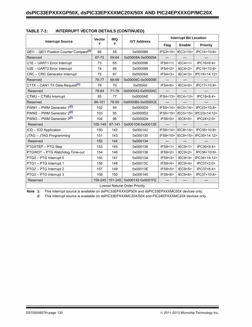
dsPIC33EPXXXGP50X, dsPIC33EPXXXMC20X/50X AND PIC24EPXXXGP/MC20X
QEI1 – QEI1 Position Counter Compare(2) 66 58 0x000088 IFS3<10> IEC3<10> IPC14<10:8>
Reserved 67-72 59-64 0x00008A-0x000094 — — —
U1E – UART1 Error Interrupt 73 65 0x000096 IFS4<1> IEC4<1> IPC16<6:4>
U2E – UART2 Error Interrupt 74 66 0x000098 IFS4<2> IEC4<2> IPC16<10:8>
CRC – CRC Generator Interrupt 75 67 0x00009A IFS4<3> IEC4<3> IPC16<14:12>
Reserved 76-77 68-69 0x00009C-0x00009E — — —
C1TX – CAN1 TX Data Request(1) 78 70 0x000A0 IFS4<6> IEC4<6> IPC17<10:8>
Reserved 79-84 71-76 0x0000A2-0x0000AC — — —
CTMU – CTMU Interrupt 85 77 0x0000AE IFS4<13> IEC4<13> IPC19<6:4>
Reserved 86-101 78-93 0x0000B0-0x0000CE — — —
PWM1 – PWM Generator 1(2) 102 94 0x0000D0 IFS5<14> IEC5<14> IPC23<10:8>
PWM2 – PWM Generator 2(2) 103 95 0x0000D2 IFS5<15> IEC5<15> IPC23<14:12>
PWM3 – PWM Generator 3(2) 104 96 0x0000D4 IFS6<0> IEC6<0> IPC24<2:0>
Reserved 105-149 97-141 0x0001D6-0x00012E — — —
ICD – ICD Application 150 142 0x000142 IFS8<14> IEC8<14> IPC35<10:8>
JTAG – JTAG Programming 151 143 0x000130 IFS8<15> IEC8<15> IPC35<14:12>
Reserved 152 144 0x000134 — — —
PTGSTEP – PTG Step 153 145 0x000136 IFS9<1> IEC9<1> IPC36<6:4>
PTGWDT – PTG Watchdog Time-out 154 146 0x000138 IFS9<2> IEC9<2> IPC36<10:8>
PTG0 – PTG Interrupt 0 155 147 0x00013A IFS9<3> IEC9<3> IPC36<14:12>
PTG1 – PTG Interrupt 1 156 148 0x00013C IFS9<4> IEC9<4> IPC37<2:0>
PTG2 – PTG Interrupt 2 157 149 0x00013E IFS9<5> IEC9<5> IPC37<6:4>
PTG3 – PTG Interrupt 3 158 150 0x000140 IFS9<6> IEC9<6> IPC37<10:8>
Reserved 159-245 151-245 0x000142-0x0001FE — — —
Lowest Natural Order Priority
TABLE 7-1: INTERRUPT VECTOR DETAILS (CONTINUED)
Interrupt SourceVector
#IRQ
#IVT Address
Interrupt Bit Location
Flag Enable Priority
Note 1: This interrupt source is available on dsPIC33EPXXXGP50X and dsPIC33EPXXXMC50X devices only.2: This interrupt source is available on dsPIC33EPXXXMC20X/50X and PIC24EPXXXMC20X devices only.
DS70000657H-page 130 2011-2013 Microchip Technology Inc.

dsPIC33EPXXXGP50X, dsPIC33EPXXXMC20X/50X AND PIC24EPXXXGP/MC20X
7.3 Interrupt Resources
Many useful resources are provided on the main prod-uct page of the Microchip web site for the devices listedin this data sheet. This product page, which can beaccessed using this link, contains the latest updatesand additional information.
7.3.1 KEY RESOURCES
• “Interrupts” (DS70600) in the “dsPIC33/PIC24 Family Reference Manual”
• Code Samples
• Application Notes
• Software Libraries
• Webinars
• All Related “dsPIC33/PIC24 Family Reference Manual” Sections
• Development Tools
7.4 Interrupt Control and Status Registers
dsPIC33EPXXXGP50X, dsPIC33EPXXXMC20X/50Xand PIC24EPXXXGP/MC20X devices implement thefollowing registers for the interrupt controller:
• INTCON1
• INTCON2
• INTCON3
• INTCON4
• INTTREG
7.4.1 INTCON1 THROUGH INTCON4
Global interrupt control functions are controlled fromINTCON1, INTCON2, INTCON3 and INTCON4.
INTCON1 contains the Interrupt Nesting Disable bit(NSTDIS), as well as the control and status flags for theprocessor trap sources.
The INTCON2 register controls external interruptrequest signal behavior and also contains the GlobalInterrupt Enable bit (GIE).
INTCON3 contains the status flags for the DMA and DOstack overflow status trap sources.
The INTCON4 register contains the softwaregenerated hard trap status bit (SGHT).
7.4.2 IFSx
The IFSx registers maintain all of the interrupt requestflags. Each source of interrupt has a status bit, which isset by the respective peripherals or external signal andis cleared via software.
7.4.3 IECx
The IECx registers maintain all of the interrupt enablebits. These control bits are used to individually enableinterrupts from the peripherals or external signals.
7.4.4 IPCx
The IPCx registers are used to set the Interrupt PriorityLevel (IPL) for each source of interrupt. Each userinterrupt source can be assigned to one of eight prioritylevels.
7.4.5 INTTREG
The INTTREG register contains the associatedinterrupt vector number and the new CPU InterruptPriority Level, which are latched into the VectorNumber bits (VECNUM<7:0>) and Interrupt PriorityLevel bits (ILR<3:0>) fields in the INTTREG register.The new Interrupt Priority Level is the priority of thepending interrupt.
The interrupt sources are assigned to the IFSx, IECxand IPCx registers in the same sequence as they arelisted in Table 7-1. For example, the INT0 (ExternalInterrupt 0) is shown as having Vector Number 8 and anatural order priority of 0. Thus, the INT0IF bit is foundin IFS0<0>, the INT0IE bit in IEC0<0> and the INT0IPbits in the first position of IPC0 (IPC0<2:0>).
7.4.6 STATUS/CONTROL REGISTERS
Although these registers are not specifically part of theinterrupt control hardware, two of the CPU Controlregisters contain bits that control interrupt functionality.For more information on these registers refer to “CPU”(DS70359) in the “dsPIC33/PIC24 Family ReferenceManual”.
• The CPU STATUS Register, SR, contains the IPL<2:0> bits (SR<7:5>). These bits indicate the current CPU Interrupt Priority Level. The user software can change the current CPU Interrupt Priority Level by writing to the IPLx bits.
• The CORCON register contains the IPL3 bit which, together with IPL<2:0>, also indicates the current CPU priority level. IPL3 is a read-only bit so that trap events cannot be masked by the user software.
All Interrupt registers are described in Register 7-3through Register 7-7 in the following pages.
Note: In the event you are not able to access theproduct page using the link above, enterthis URL in your browser:http://www.microchip.com/wwwproducts/Devices.aspx?dDocName=en555464
2011-2013 Microchip Technology Inc. DS70000657H-page 131
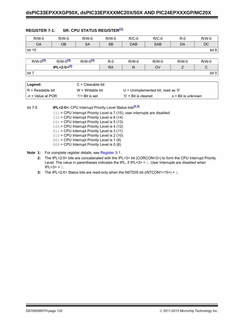
dsPIC33EPXXXGP50X, dsPIC33EPXXXMC20X/50X AND PIC24EPXXXGP/MC20X
REGISTER 7-1: SR: CPU STATUS REGISTER(1)
R/W-0 R/W-0 R/W-0 R/W-0 R/C-0 R/C-0 R-0 R/W-0
OA OB SA SB OAB SAB DA DC
bit 15 bit 8
R/W-0(3) R/W-0(3) R/W-0(3) R-0 R/W-0 R/W-0 R/W-0 R/W-0
IPL<2:0>(2) RA N OV Z C
bit 7 bit 0
Legend: C = Clearable bit
R = Readable bit W = Writable bit U = Unimplemented bit, read as ‘0’
-n = Value at POR ‘1’= Bit is set ‘0’ = Bit is cleared x = Bit is unknown
bit 7-5 IPL<2:0>: CPU Interrupt Priority Level Status bits(2,3)
111 = CPU Interrupt Priority Level is 7 (15); user interrupts are disabled 110 = CPU Interrupt Priority Level is 6 (14)101 = CPU Interrupt Priority Level is 5 (13)100 = CPU Interrupt Priority Level is 4 (12)011 = CPU Interrupt Priority Level is 3 (11)010 = CPU Interrupt Priority Level is 2 (10)001 = CPU Interrupt Priority Level is 1 (9)000 = CPU Interrupt Priority Level is 0 (8)
Note 1: For complete register details, see Register 3-1.
2: The IPL<2:0> bits are concatenated with the IPL<3> bit (CORCON<3>) to form the CPU Interrupt Priority Level. The value in parentheses indicates the IPL, if IPL<3> = 1. User interrupts are disabled when IPL<3> = 1.
3: The IPL<2:0> Status bits are read-only when the NSTDIS bit (INTCON1<15>) = 1.
DS70000657H-page 132 2011-2013 Microchip Technology Inc.

dsPIC33EPXXXGP50X, dsPIC33EPXXXMC20X/50X AND PIC24EPXXXGP/MC20X
REGISTER 7-2: CORCON: CORE CONTROL REGISTER(1)
R/W-0 U-0 R/W-0 R/W-0 R/W-0 R-0 R-0 R-0
VAR — US1 US0 EDT DL2 DL1 DL0
bit 15 bit 8
R/W-0 R/W-0 R/W-1 R/W-0 R/C-0 R-0 R/W-0 R/W-0
SATA SATB SATDW ACCSAT IPL3(2) SFA RND IF
bit 7 bit 0
Legend: C = Clearable bit
R = Readable bit W = Writable bit U = Unimplemented bit, read as ‘0’
-n = Value at POR ‘1’= Bit is set ‘0’ = Bit is cleared x = Bit is unknown
bit 15 VAR: Variable Exception Processing Latency Control bit
1 = Variable exception processing is enabled0 = Fixed exception processing is enabled
bit 3 IPL3: CPU Interrupt Priority Level Status bit 3(2)
1 = CPU Interrupt Priority Level is greater than 70 = CPU Interrupt Priority Level is 7 or less
Note 1: For complete register details, see Register 3-2.
2: The IPL3 bit is concatenated with the IPL<2:0> bits (SR<7:5>) to form the CPU Interrupt Priority Level.
2011-2013 Microchip Technology Inc. DS70000657H-page 133

dsPIC33EPXXXGP50X, dsPIC33EPXXXMC20X/50X AND PIC24EPXXXGP/MC20X
REGISTER 7-3: INTCON1: INTERRUPT CONTROL REGISTER 1
R/W-0 R/W-0 R/W-0 R/W-0 R/W-0 R/W-0 R/W-0 R/W-0
NSTDIS OVAERR(1) OVBERR(1) COVAERR(1) COVBERR(1) OVATE(1) OVBTE(1) COVTE(1)
bit 15 bit 8
R/W-0 R/W-0 R/W-0 R/W-0 R/W-0 R/W-0 R/W-0 U-0
SFTACERR(1) DIV0ERR DMACERR MATHERR ADDRERR STKERR OSCFAIL —
bit 7 bit 0
Legend:
R = Readable bit W = Writable bit U = Unimplemented bit, read as ‘0’
-n = Value at POR ‘1’ = Bit is set ‘0’ = Bit is cleared x = Bit is unknown
bit 15 NSTDIS: Interrupt Nesting Disable bit
1 = Interrupt nesting is disabled0 = Interrupt nesting is enabled
bit 14 OVAERR: Accumulator A Overflow Trap Flag bit(1)
1 = Trap was caused by overflow of Accumulator A0 = Trap was not caused by overflow of Accumulator A
bit 13 OVBERR: Accumulator B Overflow Trap Flag bit(1)
1 = Trap was caused by overflow of Accumulator B0 = Trap was not caused by overflow of Accumulator B
bit 12 COVAERR: Accumulator A Catastrophic Overflow Trap Flag bit(1)
1 = Trap was caused by catastrophic overflow of Accumulator A0 = Trap was not caused by catastrophic overflow of Accumulator A
bit 11 COVBERR: Accumulator B Catastrophic Overflow Trap Flag bit(1)
1 = Trap was caused by catastrophic overflow of Accumulator B0 = Trap was not caused by catastrophic overflow of Accumulator B
bit 10 OVATE: Accumulator A Overflow Trap Enable bit(1)
1 = Trap overflow of Accumulator A0 = Trap is disabled
bit 9 OVBTE: Accumulator B Overflow Trap Enable bit(1)
1 = Trap overflow of Accumulator B0 = Trap is disabled
bit 8 COVTE: Catastrophic Overflow Trap Enable bit(1)
1 = Trap on catastrophic overflow of Accumulator A or B is enabled0 = Trap is disabled
bit 7 SFTACERR: Shift Accumulator Error Status bit(1)
1 = Math error trap was caused by an invalid accumulator shift0 = Math error trap was not caused by an invalid accumulator shift
bit 6 DIV0ERR: Divide-by-Zero Error Status bit
1 = Math error trap was caused by a divide-by-zero0 = Math error trap was not caused by a divide-by-zero
bit 5 DMACERR: DMAC Trap Flag bit
1 = DMAC trap has occurred0 = DMAC trap has not occurred
Note 1: These bits are available on dsPIC33EPXXXMC20X/50X and dsPIC33EPXXXGP50X devices only.
DS70000657H-page 134 2011-2013 Microchip Technology Inc.

dsPIC33EPXXXGP50X, dsPIC33EPXXXMC20X/50X AND PIC24EPXXXGP/MC20X
bit 4 MATHERR: Math Error Status bit
1 = Math error trap has occurred0 = Math error trap has not occurred
bit 3 ADDRERR: Address Error Trap Status bit
1 = Address error trap has occurred0 = Address error trap has not occurred
bit 2 STKERR: Stack Error Trap Status bit
1 = Stack error trap has occurred0 = Stack error trap has not occurred
bit 1 OSCFAIL: Oscillator Failure Trap Status bit
1 = Oscillator failure trap has occurred0 = Oscillator failure trap has not occurred
bit 0 Unimplemented: Read as ‘0’
REGISTER 7-3: INTCON1: INTERRUPT CONTROL REGISTER 1 (CONTINUED)
Note 1: These bits are available on dsPIC33EPXXXMC20X/50X and dsPIC33EPXXXGP50X devices only.
2011-2013 Microchip Technology Inc. DS70000657H-page 135
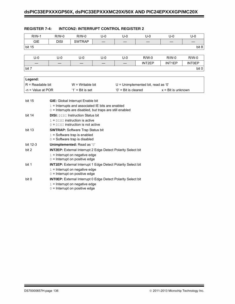
dsPIC33EPXXXGP50X, dsPIC33EPXXXMC20X/50X AND PIC24EPXXXGP/MC20X
REGISTER 7-4: INTCON2: INTERRUPT CONTROL REGISTER 2
R/W-1 R/W-0 R/W-0 U-0 U-0 U-0 U-0 U-0
GIE DISI SWTRAP — — — — —
bit 15 bit 8
U-0 U-0 U-0 U-0 U-0 R/W-0 R/W-0 R/W-0
— — — — — INT2EP INT1EP INT0EP
bit 7 bit 0
Legend:
R = Readable bit W = Writable bit U = Unimplemented bit, read as ‘0’
-n = Value at POR ‘1’ = Bit is set ‘0’ = Bit is cleared x = Bit is unknown
bit 15 GIE: Global Interrupt Enable bit
1 = Interrupts and associated IE bits are enabled 0 = Interrupts are disabled, but traps are still enabled
bit 14 DISI: DISI Instruction Status bit
1 = DISI instruction is active0 = DISI instruction is not active
bit 13 SWTRAP: Software Trap Status bit
1 = Software trap is enabled0 = Software trap is disabled
bit 12-3 Unimplemented: Read as ‘0’
bit 2 INT2EP: External Interrupt 2 Edge Detect Polarity Select bit
1 = Interrupt on negative edge 0 = Interrupt on positive edge
bit 1 INT1EP: External Interrupt 1 Edge Detect Polarity Select bit
1 = Interrupt on negative edge 0 = Interrupt on positive edge
bit 0 INT0EP: External Interrupt 0 Edge Detect Polarity Select bit
1 = Interrupt on negative edge 0 = Interrupt on positive edge
DS70000657H-page 136 2011-2013 Microchip Technology Inc.

dsPIC33EPXXXGP50X, dsPIC33EPXXXMC20X/50X AND PIC24EPXXXGP/MC20X
REGISTER 7-5: INTCON3: INTERRUPT CONTROL REGISTER 3
U-0 U-0 U-0 U-0 U-0 U-0 U-0 U-0
— — — — — — — —
bit 15 bit 8
U-0 U-0 R/W-0 R/W-0 U-0 U-0 U-0 U-0
— — DAE DOOVR — — — —
bit 7 bit 0
Legend:
R = Readable bit W = Writable bit U = Unimplemented bit, read as ‘0’
-n = Value at POR ‘1’ = Bit is set ‘0’ = Bit is cleared x = Bit is unknown
bit 15-6 Unimplemented: Read as ‘0’
bit 5 DAE: DMA Address Error Soft Trap Status bit
1 = DMA address error soft trap has occurred0 = DMA address error soft trap has not occurred
bit 4 DOOVR: DO Stack Overflow Soft Trap Status bit
1 = DO stack overflow soft trap has occurred0 = DO stack overflow soft trap has not occurred
bit 3-0 Unimplemented: Read as ‘0’
REGISTER 7-6: INTCON4: INTERRUPT CONTROL REGISTER 4
U-0 U-0 U-0 U-0 U-0 U-0 U-0 U-0
— — — — — — — —
bit 15 bit 8
U-0 U-0 U-0 U-0 U-0 U-0 U-0 R/W-0
— — — — — — — SGHT
bit 7 bit 0
Legend:
R = Readable bit W = Writable bit U = Unimplemented bit, read as ‘0’
-n = Value at POR ‘1’ = Bit is set ‘0’ = Bit is cleared x = Bit is unknown
bit 15-1 Unimplemented: Read as ‘0’
bit 0 SGHT: Software Generated Hard Trap Status bit
1 = Software generated hard trap has occurred0 = Software generated hard trap has not occurred
2011-2013 Microchip Technology Inc. DS70000657H-page 137

dsPIC33EPXXXGP50X, dsPIC33EPXXXMC20X/50X AND PIC24EPXXXGP/MC20X
REGISTER 7-7: INTTREG: INTERRUPT CONTROL AND STATUS REGISTER
U-0 U-0 U-0 U-0 R-0 R-0 R-0 R-0
— — — — ILR3 ILR2 ILR1 ILR0
bit 15 bit 8
R-0 R-0 R-0 R-0 R-0 R-0 R-0 R-0
VECNUM7 VECNUM6 VECNUM5 VECNUM4 VECNUM3 VECNUM2 VECNUM1 VECNUM0
bit 7 bit 0
Legend:
R = Readable bit W = Writable bit U = Unimplemented bit, read as ‘0’
-n = Value at POR ‘1’ = Bit is set ‘0’ = Bit is cleared x = Bit is unknown
bit 15-12 Unimplemented: Read as ‘0’
bit 11-8 ILR<3:0>: New CPU Interrupt Priority Level bits
1111 = CPU Interrupt Priority Level is 15•••0001 = CPU Interrupt Priority Level is 10000 = CPU Interrupt Priority Level is 0
bit 7-0 VECNUM<7:0>: Vector Number of Pending Interrupt bits
11111111 = 255, Reserved; do not use
•
•
•
00001001 = 9, IC1 – Input Capture 100001000 = 8, INT0 – External Interrupt 000000111 = 7, Reserved; do not use00000110 = 6, Generic soft error trap00000101 = 5, DMAC error trap00000100 = 4, Math error trap00000011 = 3, Stack error trap00000010 = 2, Generic hard trap00000001 = 1, Address error trap00000000 = 0, Oscillator fail trap
DS70000657H-page 138 2011-2013 Microchip Technology Inc.

dsPIC33EPXXXGP50X, dsPIC33EPXXXMC20X/50X AND PIC24EPXXXGP/MC20X
8.0 DIRECT MEMORY ACCESS (DMA)
The DMA Controller transfers data between PeripheralData registers and Data Space SRAM
In addition, DMA can access the entire data memoryspace. The Data Memory Bus Arbiter is utilized wheneither the CPU or DMA attempts to access SRAM,resulting in potential DMA or CPU stalls.
The DMA Controller supports 4 independent channels.Each channel can be configured for transfers to or fromselected peripherals. Some of the peripheralssupported by the DMA Controller include:
• ECAN™
• Analog-to-Digital Converter (ADC)
• Serial Peripheral Interface (SPI)
• UART
• Input Capture
• Output Compare
Refer to Table 8-1 for a complete list of supportedperipherals.
FIGURE 8-1: DMA CONTROLLER MODULE
Note 1: This data sheet summarizes thefeatures of the dsPIC33EPXXXGP50X,dsPIC33EPXXXMC20X/50X andPIC24EPXXXGP/MC20X families ofdevices. It is not intended to be acomprehensive reference source. Tocomplement the information in this datasheet, refer to “Direct Memory Access(DMA)” (DS70348) in the “dsPIC33/PIC24 Family Reference Manual”, whichis available from the Microchip web site(www.microchip.com).
2: Some registers and associated bitsdescribed in this section may not beavailable on all devices. Refer toSection 4.0 “Memory Organization” inthis data sheet for device-specific registerand bit information.
DMAPERIPHERALData Memory
SRAM
(see Figure 4-18)Arbiter
2011-2013 Microchip Technology Inc. DS70000657H-page 139
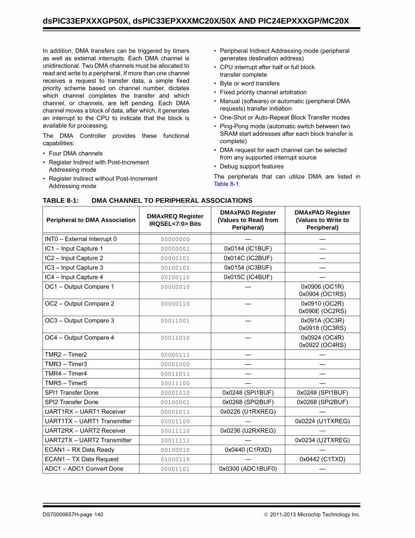
dsPIC33EPXXXGP50X, dsPIC33EPXXXMC20X/50X AND PIC24EPXXXGP/MC20X
In addition, DMA transfers can be triggered by timersas well as external interrupts. Each DMA channel isunidirectional. Two DMA channels must be allocated toread and write to a peripheral. If more than one channelreceives a request to transfer data, a simple fixedpriority scheme based on channel number, dictateswhich channel completes the transfer and whichchannel, or channels, are left pending. Each DMAchannel moves a block of data, after which, it generatesan interrupt to the CPU to indicate that the block isavailable for processing.
The DMA Controller provides these functionalcapabilities:
• Four DMA channels
• Register Indirect with Post-Increment Addressing mode
• Register Indirect without Post-Increment Addressing mode
• Peripheral Indirect Addressing mode (peripheral generates destination address)
• CPU interrupt after half or full block transfer complete
• Byte or word transfers
• Fixed priority channel arbitration
• Manual (software) or automatic (peripheral DMA requests) transfer initiation
• One-Shot or Auto-Repeat Block Transfer modes
• Ping-Pong mode (automatic switch between two SRAM start addresses after each block transfer is complete)
• DMA request for each channel can be selected from any supported interrupt source
• Debug support features
The peripherals that can utilize DMA are listed inTable 8-1.
TABLE 8-1: DMA CHANNEL TO PERIPHERAL ASSOCIATIONS
Peripheral to DMA AssociationDMAxREQ RegisterIRQSEL<7:0> Bits
DMAxPAD Register (Values to Read from
Peripheral)
DMAxPAD Register (Values to Write to
Peripheral)
INT0 – External Interrupt 0 00000000 — —
IC1 – Input Capture 1 00000001 0x0144 (IC1BUF) —
IC2 – Input Capture 2 00000101 0x014C (IC2BUF) —
IC3 – Input Capture 3 00100101 0x0154 (IC3BUF) —
IC4 – Input Capture 4 00100110 0x015C (IC4BUF) —
OC1 – Output Compare 1 00000010 — 0x0906 (OC1R)0x0904 (OC1RS)
OC2 – Output Compare 2 00000110 — 0x0910 (OC2R)0x090E (OC2RS)
OC3 – Output Compare 3 00011001 — 0x091A (OC3R)0x0918 (OC3RS)
OC4 – Output Compare 4 00011010 — 0x0924 (OC4R)0x0922 (OC4RS)
TMR2 – Timer2 00000111 — —
TMR3 – Timer3 00001000 — —
TMR4 – Timer4 00011011 — —
TMR5 – Timer5 00011100 — —
SPI1 Transfer Done 00001010 0x0248 (SPI1BUF) 0x0248 (SPI1BUF)
SPI2 Transfer Done 00100001 0x0268 (SPI2BUF) 0x0268 (SPI2BUF)
UART1RX – UART1 Receiver 00001011 0x0226 (U1RXREG) —
UART1TX – UART1 Transmitter 00001100 — 0x0224 (U1TXREG)
UART2RX – UART2 Receiver 00011110 0x0236 (U2RXREG) —
UART2TX – UART2 Transmitter 00011111 — 0x0234 (U2TXREG)
ECAN1 – RX Data Ready 00100010 0x0440 (C1RXD) —
ECAN1 – TX Data Request 01000110 — 0x0442 (C1TXD)
ADC1 – ADC1 Convert Done 00001101 0x0300 (ADC1BUF0) —
DS70000657H-page 140 2011-2013 Microchip Technology Inc.

dsPIC33EPXXXGP50X, dsPIC33EPXXXMC20X/50X AND PIC24EPXXXGP/MC20X
FIGURE 8-2: DMA CONTROLLER BLOCK DIAGRAM
8.1 DMA Resources
Many useful resources are provided on the main prod-uct page of the Microchip web site for the devices listedin this data sheet. This product page, which can beaccessed using this link, contains the latest updatesand additional information.
8.1.1 KEY RESOURCES
• Section 22. “Direct Memory Access (DMA)” (DS70348) in the “dsPIC33/PIC24 Family Reference Manual”
• Code Samples
• Application Notes
• Software Libraries
• Webinars
• All Related “dsPIC33/PIC24 Family Reference Manual” Sections
• Development Tools
8.2 DMAC Registers
Each DMAC Channel x (where x = 0 through 3)contains the following registers:
• 16-Bit DMA Channel Control register (DMAxCON)
• 16-Bit DMA Channel IRQ Select register (DMAxREQ)
• 32-Bit DMA RAM Primary Start Address register (DMAxSTA)
• 32-Bit DMA RAM Secondary Start Address register (DMAxSTB)
• 16-Bit DMA Peripheral Address register (DMAxPAD)
• 14-Bit DMA Transfer Count register (DMAxCNT)
Additional status registers (DMAPWC, DMARQC,DMAPPS, DMALCA and DSADR) are common to allDMAC channels. These status registers provide infor-mation on write and request collisions, as well as onlast address and channel access information.
The interrupt flags (DMAxIF) are located in an IFSxregister in the interrupt controller. The correspondinginterrupt enable control bits (DMAxIE) are located inan IECx register in the interrupt controller, and thecorresponding interrupt priority control bits (DMAxIP)are located in an IPCx register in the interruptcontroller.
CPU
Arbiter
PeripheralNon-DMA
DMA X-Bus
Peripheral Indirect Address
DM
AC
on
tro
l
DMA Controller
DMA
CPU Peripheral X-Bus
IRQ to DMA and Interrupt
Controller Modules
IRQ to DMA and Interrupt Controller
Modules
IRQ to DMA and Interrupt Controller
Modules
0 1 2 3
SRAM
Channels Peripheral 1
DMAReady
CPU DMA
Peripheral 3
DMAReady
CPU DMA
Peripheral 2
DMAReady
CPU DMA
Note: CPU and DMA address buses are not shown for clarity.
Note: In the event you are not able to access theproduct page using the link above, enterthis URL in your browser:http://www.microchip.com/wwwproducts/Devices.aspx?dDocName=en555464
2011-2013 Microchip Technology Inc. DS70000657H-page 141

dsPIC33EPXXXGP50X, dsPIC33EPXXXMC20X/50X AND PIC24EPXXXGP/MC20X
REGISTER 8-1: DMAXCON: DMA CHANNEL X CONTROL REGISTER
R/W-0 R/W-0 R/W-0 R/W-0 R/W-0 U-0 U-0 U-0
CHEN SIZE DIR HALF NULLW — — —
bit 15 bit 8
U-0 U-0 R/W-0 R/W-0 U-0 U-0 R/W-0 R/W-0
— — AMODE1 AMODE0 — — MODE1 MODE0
bit 7 bit 0
Legend:
R = Readable bit W = Writable bit U = Unimplemented bit, read as ‘0’
-n = Value at POR ‘1’ = Bit is set ‘0’ = Bit is cleared x = Bit is unknown
bit 15 CHEN: DMA Channel Enable bit
1 = Channel is enabled0 = Channel is disabled
bit 14 SIZE: DMA Data Transfer Size bit
1 = Byte0 = Word
bit 13 DIR: DMA Transfer Direction bit (source/destination bus select)
1 = Reads from RAM address, writes to peripheral address0 = Reads from peripheral address, writes to RAM address
bit 12 HALF: DMA Block Transfer Interrupt Select bit
1 = Initiates interrupt when half of the data has been moved0 = Initiates interrupt when all of the data has been moved
bit 11 NULLW: Null Data Peripheral Write Mode Select bit
1 = Null data write to peripheral in addition to RAM write (DIR bit must also be clear)0 = Normal operation
bit 10-6 Unimplemented: Read as ‘0’
bit 5-4 AMODE<1:0>: DMA Channel Addressing Mode Select bits
11 = Reserved 10 = Peripheral Indirect Addressing mode01 = Register Indirect without Post-Increment mode00 = Register Indirect with Post-Increment mode
bit 3-2 Unimplemented: Read as ‘0’
bit 1-0 MODE<1:0>: DMA Channel Operating Mode Select bits
11 = One-Shot, Ping-Pong modes are enabled (one block transfer from/to each DMA buffer)10 = Continuous, Ping-Pong modes are enabled01 = One-Shot, Ping-Pong modes are disabled00 = Continuous, Ping-Pong modes are disabled
DS70000657H-page 142 2011-2013 Microchip Technology Inc.

dsPIC33EPXXXGP50X, dsPIC33EPXXXMC20X/50X AND PIC24EPXXXGP/MC20X
REGISTER 8-2: DMAXREQ: DMA CHANNEL X IRQ SELECT REGISTER
R/S-0 U-0 U-0 U-0 U-0 U-0 U-0 U-0
FORCE(1) — — — — — — —
bit 15 bit 8
R/W-0 R/W-0 R/W-0 R/W-0 R/W-0 R/W-0 R/W-0 R/W-0
IRQSEL7 IRQSEL6 IRQSEL5 IRQSEL4 IRQSEL3 IRQSEL2 IRQSEL1 IRQSEL0
bit 7 bit 0
Legend: S = Settable bit
R = Readable bit W = Writable bit U = Unimplemented bit, read as ‘0’
-n = Value at POR ‘1’ = Bit is set ‘0’ = Bit is cleared x = Bit is unknown
bit 15 FORCE: Force DMA Transfer bit(1)
1 = Forces a single DMA transfer (Manual mode)0 = Automatic DMA transfer initiation by DMA request
bit 14-8 Unimplemented: Read as ‘0’
bit 7-0 IRQSEL<7:0>: DMA Peripheral IRQ Number Select bits
01000110 = ECAN1 – TX Data Request(2)
00100110 = IC4 – Input Capture 400100101 = IC3 – Input Capture 300100010 = ECAN1 – RX Data Ready(2)
00100001 = SPI2 Transfer Done00011111 = UART2TX – UART2 Transmitter00011110 = UART2RX – UART2 Receiver00011100 = TMR5 – Timer500011011 = TMR4 – Timer400011010 = OC4 – Output Compare 400011001 = OC3 – Output Compare 300001101 = ADC1 – ADC1 Convert done00001100 = UART1TX – UART1 Transmitter00001011 = UART1RX – UART1 Receiver00001010 = SPI1 – Transfer Done00001000 = TMR3 – Timer300000111 = TMR2 – Timer200000110 = OC2 – Output Compare 200000101 = IC2 – Input Capture 200000010 = OC1 – Output Compare 100000001 = IC1 – Input Capture 100000000 = INT0 – External Interrupt 0
Note 1: The FORCE bit cannot be cleared by user software. The FORCE bit is cleared by hardware when the forced DMA transfer is complete or the channel is disabled (CHEN = 0).
2: This selection is available in dsPIC33EPXXXGP/MC50X devices only.
2011-2013 Microchip Technology Inc. DS70000657H-page 143
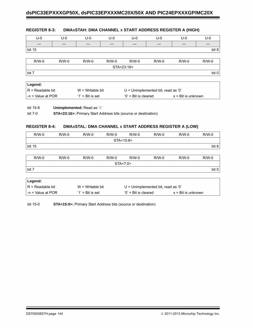
dsPIC33EPXXXGP50X, dsPIC33EPXXXMC20X/50X AND PIC24EPXXXGP/MC20X
REGISTER 8-3: DMAXSTAH: DMA CHANNEL X START ADDRESS REGISTER A (HIGH)
U-0 U-0 U-0 U-0 U-0 U-0 U-0 U-0
— — — — — — — —
bit 15 bit 8
R/W-0 R/W-0 R/W-0 R/W-0 R/W-0 R/W-0 R/W-0 R/W-0
STA<23:16>
bit 7 bit 0
Legend:
R = Readable bit W = Writable bit U = Unimplemented bit, read as ‘0’
-n = Value at POR ‘1’ = Bit is set ‘0’ = Bit is cleared x = Bit is unknown
bit 15-8 Unimplemented: Read as ‘0’
bit 7-0 STA<23:16>: Primary Start Address bits (source or destination)
REGISTER 8-4: DMAXSTAL: DMA CHANNEL X START ADDRESS REGISTER A (LOW)
R/W-0 R/W-0 R/W-0 R/W-0 R/W-0 R/W-0 R/W-0 R/W-0
STA<15:8>
bit 15 bit 8
R/W-0 R/W-0 R/W-0 R/W-0 R/W-0 R/W-0 R/W-0 R/W-0
STA<7:0>
bit 7 bit 0
Legend:
R = Readable bit W = Writable bit U = Unimplemented bit, read as ‘0’
-n = Value at POR ‘1’ = Bit is set ‘0’ = Bit is cleared x = Bit is unknown
bit 15-0 STA<15:0>: Primary Start Address bits (source or destination)
DS70000657H-page 144 2011-2013 Microchip Technology Inc.

dsPIC33EPXXXGP50X, dsPIC33EPXXXMC20X/50X AND PIC24EPXXXGP/MC20X
REGISTER 8-5: DMAXSTBH: DMA CHANNEL X START ADDRESS REGISTER B (HIGH)
U-0 U-0 U-0 U-0 U-0 U-0 U-0 U-0
— — — — — — — —
bit 15 bit 8
R/W-0 R/W-0 R/W-0 R/W-0 R/W-0 R/W-0 R/W-0 R/W-0
STB<23:16>
bit 7 bit 0
Legend:
R = Readable bit W = Writable bit U = Unimplemented bit, read as ‘0’
-n = Value at POR ‘1’ = Bit is set ‘0’ = Bit is cleared x = Bit is unknown
bit 15-8 Unimplemented: Read as ‘0’
bit 7-0 STB<23:16>: Secondary Start Address bits (source or destination)
REGISTER 8-6: DMAXSTBL: DMA CHANNEL X START ADDRESS REGISTER B (LOW)
R/W-0 R/W-0 R/W-0 R/W-0 R/W-0 R/W-0 R/W-0 R/W-0
STB<15:8>
bit 15 bit 8
R/W-0 R/W-0 R/W-0 R/W-0 R/W-0 R/W-0 R/W-0 R/W-0
STB<7:0>
bit 7 bit 0
Legend:
R = Readable bit W = Writable bit U = Unimplemented bit, read as ‘0’
-n = Value at POR ‘1’ = Bit is set ‘0’ = Bit is cleared x = Bit is unknown
bit 15-0 STB<15:0>: Secondary Start Address bits (source or destination)
2011-2013 Microchip Technology Inc. DS70000657H-page 145

dsPIC33EPXXXGP50X, dsPIC33EPXXXMC20X/50X AND PIC24EPXXXGP/MC20X
REGISTER 8-7: DMAXPAD: DMA CHANNEL X PERIPHERAL ADDRESS REGISTER(1)
R/W-0 R/W-0 R/W-0 R/W-0 R/W-0 R/W-0 R/W-0 R/W-0
PAD<15:8>
bit 15 bit 8
R/W-0 R/W-0 R/W-0 R/W-0 R/W-0 R/W-0 R/W-0 R/W-0
PAD<7:0>
bit 7 bit 0
Legend:
R = Readable bit W = Writable bit U = Unimplemented bit, read as ‘0’
-n = Value at POR ‘1’ = Bit is set ‘0’ = Bit is cleared x = Bit is unknown
bit 15-0 PAD<15:0>: Peripheral Address Register bits
Note 1: If the channel is enabled (i.e., active), writes to this register may result in unpredictable behavior of the DMA channel and should be avoided.
REGISTER 8-8: DMAXCNT: DMA CHANNEL X TRANSFER COUNT REGISTER(1)
U-0 U-0 R/W-0 R/W-0 R/W-0 R/W-0 R/W-0 R/W-0
— — CNT<13:8>(2)
bit 15 bit 8
R/W-0 R/W-0 R/W-0 R/W-0 R/W-0 R/W-0 R/W-0 R/W-0
CNT<7:0>(2)
bit 7 bit 0
Legend:
R = Readable bit W = Writable bit U = Unimplemented bit, read as ‘0’
-n = Value at POR ‘1’ = Bit is set ‘0’ = Bit is cleared x = Bit is unknown
bit 15-14 Unimplemented: Read as ‘0’
bit 13-0 CNT<13:0>: DMA Transfer Count Register bits(2)
Note 1: If the channel is enabled (i.e., active), writes to this register may result in unpredictable behavior of the DMA channel and should be avoided.
2: The number of DMA transfers = CNT<13:0> + 1.
DS70000657H-page 146 2011-2013 Microchip Technology Inc.

dsPIC33EPXXXGP50X, dsPIC33EPXXXMC20X/50X AND PIC24EPXXXGP/MC20X
REGISTER 8-9: DSADRH: DMA MOST RECENT RAM HIGH ADDRESS REGISTER
U-0 U-0 U-0 U-0 U-0 U-0 U-0 U-0
— — — — — — — —
bit 15 bit 8
R-0 R-0 R-0 R-0 R-0 R-0 R-0 R-0
DSADR<23:16>
bit 7 bit 0
Legend:
R = Readable bit W = Writable bit U = Unimplemented bit, read as ‘0’
-n = Value at POR ‘1’ = Bit is set ‘0’ = Bit is cleared x = Bit is unknown
bit 15-8 Unimplemented: Read as ‘0’
bit 7-0 DSADR<23:16>: Most Recent DMA Address Accessed by DMA bits
REGISTER 8-10: DSADRL: DMA MOST RECENT RAM LOW ADDRESS REGISTER
R-0 R-0 R-0 R-0 R-0 R-0 R-0 R-0
DSADR<15:8>
bit 15 bit 8
R-0 R-0 R-0 R-0 R-0 R-0 R-0 R-0
DSADR<7:0>
bit 7 bit 0
Legend:
R = Readable bit W = Writable bit U = Unimplemented bit, read as ‘0’
-n = Value at POR ‘1’ = Bit is set ‘0’ = Bit is cleared x = Bit is unknown
bit 15-0 DSADR<15:0>: Most Recent DMA Address Accessed by DMA bits
2011-2013 Microchip Technology Inc. DS70000657H-page 147
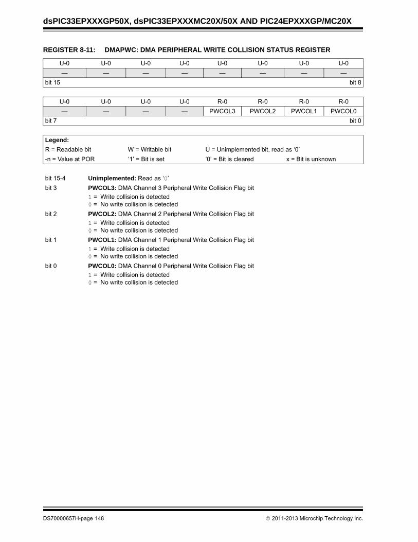
dsPIC33EPXXXGP50X, dsPIC33EPXXXMC20X/50X AND PIC24EPXXXGP/MC20X
REGISTER 8-11: DMAPWC: DMA PERIPHERAL WRITE COLLISION STATUS REGISTER
U-0 U-0 U-0 U-0 U-0 U-0 U-0 U-0
— — — — — — — —
bit 15 bit 8
U-0 U-0 U-0 U-0 R-0 R-0 R-0 R-0
— — — — PWCOL3 PWCOL2 PWCOL1 PWCOL0
bit 7 bit 0
Legend:
R = Readable bit W = Writable bit U = Unimplemented bit, read as ‘0’
-n = Value at POR ‘1’ = Bit is set ‘0’ = Bit is cleared x = Bit is unknown
bit 15-4 Unimplemented: Read as ‘0’
bit 3 PWCOL3: DMA Channel 3 Peripheral Write Collision Flag bit
1 = Write collision is detected0 = No write collision is detected
bit 2 PWCOL2: DMA Channel 2 Peripheral Write Collision Flag bit
1 = Write collision is detected0 = No write collision is detected
bit 1 PWCOL1: DMA Channel 1 Peripheral Write Collision Flag bit
1 = Write collision is detected0 = No write collision is detected
bit 0 PWCOL0: DMA Channel 0 Peripheral Write Collision Flag bit
1 = Write collision is detected0 = No write collision is detected
DS70000657H-page 148 2011-2013 Microchip Technology Inc.

dsPIC33EPXXXGP50X, dsPIC33EPXXXMC20X/50X AND PIC24EPXXXGP/MC20X
REGISTER 8-12: DMARQC: DMA REQUEST COLLISION STATUS REGISTER
U-0 U-0 U-0 U-0 U-0 U-0 U-0 U-0
— — — — — — — —
bit 15 bit 8
U-0 U-0 U-0 U-0 R-0 R-0 R-0 R-0
— — — — RQCOL3 RQCOL2 RQCOL1 RQCOL0
bit 7 bit 0
Legend:
R = Readable bit W = Writable bit U = Unimplemented bit, read as ‘0’
-n = Value at POR ‘1’ = Bit is set ‘0’ = Bit is cleared x = Bit is unknown
bit 15-4 Unimplemented: Read as ‘0’
bit 3 RQCOL3: DMA Channel 3 Transfer Request Collision Flag bit
1 = User force and interrupt-based request collision is detected0 = No request collision is detected
bit 2 RQCOL2: DMA Channel 2 Transfer Request Collision Flag bit
1 = User force and interrupt-based request collision is detected0 = No request collision is detected
bit 1 RQCOL1: DMA Channel 1 Transfer Request Collision Flag bit
1 = User force and interrupt-based request collision is detected0 = No request collision is detected
bit 0 RQCOL0: DMA Channel 0 Transfer Request Collision Flag bit
1 = User force and interrupt-based request collision is detected0 = No request collision is detected
2011-2013 Microchip Technology Inc. DS70000657H-page 149

dsPIC33EPXXXGP50X, dsPIC33EPXXXMC20X/50X AND PIC24EPXXXGP/MC20X
REGISTER 8-13: DMALCA: DMA LAST CHANNEL ACTIVE STATUS REGISTER
U-0 U-0 U-0 U-0 U-0 U-0 U-0 U-0
— — — — — — — —
bit 15 bit 8
U-0 U-0 U-0 U-0 R-1 R-1 R-1 R-1
— — — — LSTCH<3:0>
bit 7 bit 0
Legend:
R = Readable bit W = Writable bit U = Unimplemented bit, read as ‘0’
-n = Value at POR ‘1’ = Bit is set ‘0’ = Bit is cleared x = Bit is unknown
bit 15-4 Unimplemented: Read as ‘0’
bit 3-0 LSTCH<3:0>: Last DMAC Channel Active Status bits
1111 = No DMA transfer has occurred since system Reset1110 = Reserved
•
•
•
0100 = Reserved0011 = Last data transfer was handled by Channel 30010 = Last data transfer was handled by Channel 20001 = Last data transfer was handled by Channel 10000 = Last data transfer was handled by Channel 0
DS70000657H-page 150 2011-2013 Microchip Technology Inc.

dsPIC33EPXXXGP50X, dsPIC33EPXXXMC20X/50X AND PIC24EPXXXGP/MC20X
REGISTER 8-14: DMAPPS: DMA PING-PONG STATUS REGISTER
U-0 U-0 U-0 U-0 U-0 U-0 U-0 U-0
— — — — — — — —
bit 15 bit 8
U-0 U-0 U-0 U-0 R-0 R-0 R-0 R-0
— — — — PPST3 PPST2 PPST1 PPST0
bit 7 bit 0
Legend:
R = Readable bit W = Writable bit U = Unimplemented bit, read as ‘0’
-n = Value at POR ‘1’ = Bit is set ‘0’ = Bit is cleared x = Bit is unknown
bit 15-4 Unimplemented: Read as ‘0’
bit 3 PPST3: DMA Channel 3 Ping-Pong Mode Status Flag bit
1 = DMASTB3 register is selected0 = DMASTA3 register is selected
bit 2 PPST2: DMA Channel 2 Ping-Pong Mode Status Flag bit
1 = DMASTB2 register is selected0 = DMASTA2 register is selected
bit 1 PPST1: DMA Channel 1 Ping-Pong Mode Status Flag bit
1 = DMASTB1 register is selected0 = DMASTA1 register is selected
bit 0 PPST0: DMA Channel 0 Ping-Pong Mode Status Flag bit
1 = DMASTB0 register is selected0 = DMASTA0 register is selected
2011-2013 Microchip Technology Inc. DS70000657H-page 151

dsPIC33EPXXXGP50X, dsPIC33EPXXXMC20X/50X AND PIC24EPXXXGP/MC20X
NOTES:
DS70000657H-page 152 2011-2013 Microchip Technology Inc.

dsPIC33EPXXXGP50X, dsPIC33EPXXXMC20X/50X AND PIC24EPXXXGP/MC20X
9.0 OSCILLATOR CONFIGURATION The dsPIC33EPXXXGP50X, dsPIC33EPXXXMC20X/50X and PIC24EPXXXGP/MC20X oscillator systemprovides:
• On-chip Phase-Locked Loop (PLL) to boost internal operating frequency on select internal and external oscillator sources
• On-the-fly clock switching between various clock sources
• Doze mode for system power savings• Fail-Safe Clock Monitor (FSCM) that detects clock
failure and permits safe application recovery or shutdown
• Configuration bits for clock source selection
A simplified diagram of the oscillator system is shownin Figure 9-1.
FIGURE 9-1: OSCILLATOR SYSTEM DIAGRAM
Note 1: This data sheet summarizes thefeatures of the dsPIC33EPXXXGP50X,dsPIC33EPXXXMC20X/50X andPIC24EPXXXGP/MC20X families ofdevices. It is not intended to be a compre-hensive reference source. To complementthe information in this data sheet, refer to“Oscillator” (DS70580) in the “dsPIC33/PIC24 Family Reference Manual”, which isavailable from the Microchip web site(www.microchip.com).
2: Some registers and associated bitsdescribed in this section may not beavailable on all devices. Refer toSection 4.0 “Memory Organization” inthis data sheet for device-specific registerand bit information.
Note 1: See Figure 9-2 for PLL details.2: The term, FP, refers to the clock source for all peripherals, while FCY refers to the clock source for the CPU.
Throughout this document, FCY and FP are used interchangeably, except in the case of Doze mode. FP and FCY will be different when Doze mode is used with a doze ratio of 1:2 or lower.
XTPLL, HSPLL, ECPLL,
XT, HS, EC
FRCDIV<2:0>
WDT, PWRT,
FRCDIVN
FRCDIV16
NOSC<2:0> FNOSC<2:0>
Reset
FRCOscillator
LPRCOscillator
DOZE<2:0>
S3
S1
S2
S1/S3
S7
S6
FRC
LPRC
S0
S5
÷ 16
Clock Switch
0b000
Clock Fail
÷ 2
TUN<5:0>
PLL(1)
FCY(2)
FOSC
FR
CD
IV
DO
ZE
FSCM
POSCCLK
FRCCLK
OSC2
OSC1Primary Oscillator
POSCMD<1:0>FP(2)
÷ N
ROSEL RODIV<3:0>
REFCLKO
POSCCLK
RPnFOSC
Reference Clock Generation
FRCPLL, FPLLO
COSC<2:0>
2011-2013 Microchip Technology Inc. DS70000657H-page 153

dsPIC33EPXXXGP50X, dsPIC33EPXXXMC20X/50X AND PIC24EPXXXGP/MC20X
9.1 CPU Clocking System
The dsPIC33EPXXXGP50X, dsPIC33EPXXXMC20X/50X and PIC24EPXXXGP/MC20X family of devicesprovides six system clock options:
• Fast RC (FRC) Oscillator
• FRC Oscillator with Phase Locked Loop (PLL)
• FRC Oscillator with Postscaler
• Primary (XT, HS or EC) Oscillator
• Primary Oscillator with PLL
• Low-Power RC (LPRC) Oscillator
Instruction execution speed or device operatingfrequency, FCY, is given by Equation 9-1.
EQUATION 9-1: DEVICE OPERATING FREQUENCY
Figure 9-2 is a block diagram of the PLL module.
Equation 9-2 provides the relationship between inputfrequency (FIN) and output frequency (FPLLO). In clockmodes S1 and S3, when the PLL output is selected,FOSC = FPLLO.
Equation 9-3 provides the relationship between inputfrequency (FIN) and VCO frequency (FVCO).
FIGURE 9-2: PLL BLOCK DIAGRAM
EQUATION 9-2: FPLLO CALCULATION
EQUATION 9-3: FVCO CALCULATION
FCY = Fosc/2
÷ N1
÷ M
÷ N2PFD VCO
PLLPRE<4:0>
PLLDIV<8:0>
PLLPOST<1:0>
0.8 MHz < FPLLI(1) < 8.0 MHz120 MHZ < FVCO(1) < 340 MHZ
FPLLO(1) 120 MHz @ +125ºC
FIN FPLLI FVCO FPLLO
Note 1: This frequency range must be met at all times.
FPLLO(1) 140 MHz @ +85ºC
To FOSC clock multiplexer
FPLLO FINM
N1 N2--------------------- FIN
PLLDIV 2+ PLLPRE 2+ 2 PLLPOST 1+
---------------------------------------------------------------------------------------- = =
Where:
N1 = PLLPRE + 2
N2 = 2 x (PLLPOST + 1)
M = PLLDIV + 2
Fvco FINMN1------- FIN
PLLDIV 2+ PLLPRE 2+
------------------------------------- = =
DS70000657H-page 154 2011-2013 Microchip Technology Inc.

dsPIC33EPXXXGP50X, dsPIC33EPXXXMC20X/50X AND PIC24EPXXXGP/MC20X
TABLE 9-1: CONFIGURATION BIT VALUES FOR CLOCK SELECTION
9.2 Oscillator Resources
Many useful resources are provided on the main prod-uct page of the Microchip web site for the devices listedin this data sheet. This product page, which can beaccessed using this link, contains the latest updatesand additional information.
9.2.1 KEY RESOURCES
• “Oscillator” (DS70580) in the “dsPIC33/PIC24 Family Reference Manual”
• Code Samples
• Application Notes
• Software Libraries
• Webinars
• All Related “dsPIC33/PIC24 Family Reference Manual” Sections
• Development Tools
Oscillator Mode Oscillator Source POSCMD<1:0> FNOSC<2:0>See
Notes
Fast RC Oscillator with Divide-by-N (FRCDIVN) Internal xx 111 1, 2
Fast RC Oscillator with Divide-by-16 (FRCDIV16) Internal xx 110 1
Low-Power RC Oscillator (LPRC) Internal xx 101 1
Primary Oscillator (HS) with PLL (HSPLL) Primary 10 011
Primary Oscillator (XT) with PLL (XTPLL) Primary 01 011
Primary Oscillator (EC) with PLL (ECPLL) Primary 00 011 1
Primary Oscillator (HS) Primary 10 010
Primary Oscillator (XT) Primary 01 010
Primary Oscillator (EC) Primary 00 010 1
Fast RC Oscillator (FRC) with Divide-by-N and PLL (FRCPLL)
Internal xx 001 1
Fast RC Oscillator (FRC) Internal xx 000 1
Note 1: OSC2 pin function is determined by the OSCIOFNC Configuration bit.
2: This is the default oscillator mode for an unprogrammed (erased) device.
Note: In the event you are not able to access theproduct page using the link above, enterthis URL in your browser:http://www.microchip.com/wwwproducts/Devices.aspx?dDocName=en555464
2011-2013 Microchip Technology Inc. DS70000657H-page 155
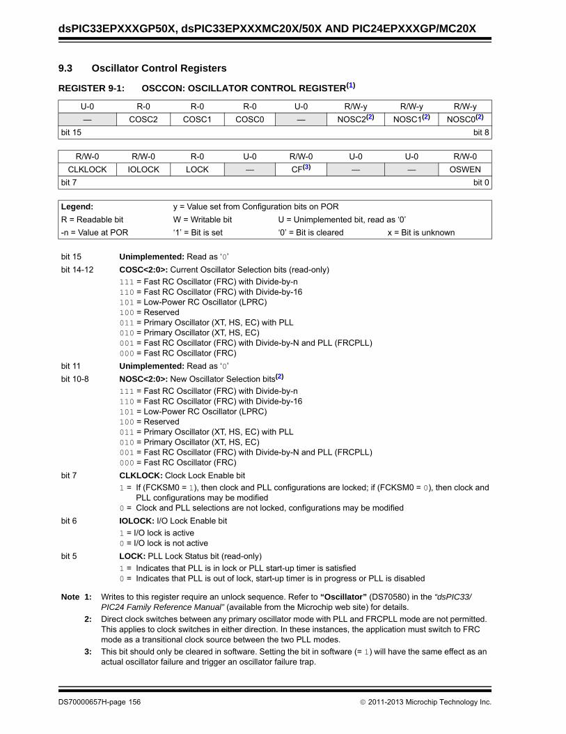
dsPIC33EPXXXGP50X, dsPIC33EPXXXMC20X/50X AND PIC24EPXXXGP/MC20X
9.3 Oscillator Control Registers
REGISTER 9-1: OSCCON: OSCILLATOR CONTROL REGISTER(1)
U-0 R-0 R-0 R-0 U-0 R/W-y R/W-y R/W-y
— COSC2 COSC1 COSC0 — NOSC2(2) NOSC1(2) NOSC0(2)
bit 15 bit 8
R/W-0 R/W-0 R-0 U-0 R/W-0 U-0 U-0 R/W-0
CLKLOCK IOLOCK LOCK — CF(3) — — OSWEN
bit 7 bit 0
Legend: y = Value set from Configuration bits on POR
R = Readable bit W = Writable bit U = Unimplemented bit, read as ‘0’
-n = Value at POR ‘1’ = Bit is set ‘0’ = Bit is cleared x = Bit is unknown
bit 15 Unimplemented: Read as ‘0’
bit 14-12 COSC<2:0>: Current Oscillator Selection bits (read-only)
111 = Fast RC Oscillator (FRC) with Divide-by-n110 = Fast RC Oscillator (FRC) with Divide-by-16101 = Low-Power RC Oscillator (LPRC)100 = Reserved011 = Primary Oscillator (XT, HS, EC) with PLL 010 = Primary Oscillator (XT, HS, EC)001 = Fast RC Oscillator (FRC) with Divide-by-N and PLL (FRCPLL) 000 = Fast RC Oscillator (FRC)
bit 11 Unimplemented: Read as ‘0’
bit 10-8 NOSC<2:0>: New Oscillator Selection bits(2)
111 = Fast RC Oscillator (FRC) with Divide-by-n110 = Fast RC Oscillator (FRC) with Divide-by-16101 = Low-Power RC Oscillator (LPRC)100 = Reserved011 = Primary Oscillator (XT, HS, EC) with PLL010 = Primary Oscillator (XT, HS, EC)001 = Fast RC Oscillator (FRC) with Divide-by-N and PLL (FRCPLL)000 = Fast RC Oscillator (FRC)
bit 7 CLKLOCK: Clock Lock Enable bit
1 = If (FCKSM0 = 1), then clock and PLL configurations are locked; if (FCKSM0 = 0), then clock andPLL configurations may be modified
0 = Clock and PLL selections are not locked, configurations may be modified
bit 6 IOLOCK: I/O Lock Enable bit
1 = I/O lock is active0 = I/O lock is not active
bit 5 LOCK: PLL Lock Status bit (read-only)
1 = Indicates that PLL is in lock or PLL start-up timer is satisfied0 = Indicates that PLL is out of lock, start-up timer is in progress or PLL is disabled
Note 1: Writes to this register require an unlock sequence. Refer to “Oscillator” (DS70580) in the “dsPIC33/PIC24 Family Reference Manual” (available from the Microchip web site) for details.
2: Direct clock switches between any primary oscillator mode with PLL and FRCPLL mode are not permitted. This applies to clock switches in either direction. In these instances, the application must switch to FRC mode as a transitional clock source between the two PLL modes.
3: This bit should only be cleared in software. Setting the bit in software (= 1) will have the same effect as an actual oscillator failure and trigger an oscillator failure trap.
DS70000657H-page 156 2011-2013 Microchip Technology Inc.

dsPIC33EPXXXGP50X, dsPIC33EPXXXMC20X/50X AND PIC24EPXXXGP/MC20X
bit 4 Unimplemented: Read as ‘0’
bit 3 CF: Clock Fail Detect bit(3)
1 = FSCM has detected clock failure0 = FSCM has not detected clock failure
bit 2-1 Unimplemented: Read as ‘0’
bit 0 OSWEN: Oscillator Switch Enable bit
1 = Requests oscillator switch to selection specified by the NOSC<2:0> bits0 = Oscillator switch is complete
REGISTER 9-1: OSCCON: OSCILLATOR CONTROL REGISTER(1) (CONTINUED)
Note 1: Writes to this register require an unlock sequence. Refer to “Oscillator” (DS70580) in the “dsPIC33/PIC24 Family Reference Manual” (available from the Microchip web site) for details.
2: Direct clock switches between any primary oscillator mode with PLL and FRCPLL mode are not permitted. This applies to clock switches in either direction. In these instances, the application must switch to FRC mode as a transitional clock source between the two PLL modes.
3: This bit should only be cleared in software. Setting the bit in software (= 1) will have the same effect as an actual oscillator failure and trigger an oscillator failure trap.
2011-2013 Microchip Technology Inc. DS70000657H-page 157

dsPIC33EPXXXGP50X, dsPIC33EPXXXMC20X/50X AND PIC24EPXXXGP/MC20X
REGISTER 9-2: CLKDIV: CLOCK DIVISOR REGISTER
R/W-0 R/W-0 R/W-1 R/W-1 R/W-0 R/W-0 R/W-0 R/W-0
ROI DOZE2(1) DOZE1(1) DOZE0(1) DOZEN(2,3) FRCDIV2 FRCDIV1 FRCDIV0
bit 15 bit 8
R/W-0 R/W-1 U-0 R/W-0 R/W-0 R/W-0 R/W-0 R/W-0
PLLPOST1 PLLPOST0 — PLLPRE4 PLLPRE3 PLLPRE2 PLLPRE1 PLLPRE0
bit 7 bit 0
Legend:
R = Readable bit W = Writable bit U = Unimplemented bit, read as ‘0’
-n = Value at POR ‘1’ = Bit is set ‘0’ = Bit is cleared x = Bit is unknown
bit 15 ROI: Recover on Interrupt bit
1 = Interrupts will clear the DOZEN bit0 = Interrupts have no effect on the DOZEN bit
bit 14-12 DOZE<2:0>: Processor Clock Reduction Select bits(1)
111 = FCY divided by 128110 = FCY divided by 64101 = FCY divided by 32100 = FCY divided by 16011 = FCY divided by 8 (default)010 = FCY divided by 4001 = FCY divided by 2000 = FCY divided by 1
bit 11 DOZEN: Doze Mode Enable bit(2,3)
1 = DOZE<2:0> field specifies the ratio between the peripheral clocks and the processor clocks0 = Processor clock and peripheral clock ratio is forced to 1:1
bit 10-8 FRCDIV<2:0>: Internal Fast RC Oscillator Postscaler bits
111 = FRC divided by 256110 = FRC divided by 64101 = FRC divided by 32100 = FRC divided by 16011 = FRC divided by 8010 = FRC divided by 4001 = FRC divided by 2000 = FRC divided by 1 (default)
bit 7-6 PLLPOST<1:0>: PLL VCO Output Divider Select bits (also denoted as ‘N2’, PLL postscaler)
11 = Output divided by 810 = Reserved01 = Output divided by 4 (default)00 = Output divided by 2
bit 5 Unimplemented: Read as ‘0’
Note 1: The DOZE<2:0> bits can only be written to when the DOZEN bit is clear. If DOZEN = 1, any writes to DOZE<2:0> are ignored.
2: This bit is cleared when the ROI bit is set and an interrupt occurs.
3: The DOZEN bit cannot be set if DOZE<2:0> = 000. If DOZE<2:0> = 000, any attempt by user software to set the DOZEN bit is ignored.
DS70000657H-page 158 2011-2013 Microchip Technology Inc.

dsPIC33EPXXXGP50X, dsPIC33EPXXXMC20X/50X AND PIC24EPXXXGP/MC20X
bit 4-0 PLLPRE<4:0>: PLL Phase Detector Input Divider Select bits (also denoted as ‘N1’, PLL prescaler)
11111 = Input divided by 33•••00001 = Input divided by 300000 = Input divided by 2 (default)
REGISTER 9-2: CLKDIV: CLOCK DIVISOR REGISTER (CONTINUED)
Note 1: The DOZE<2:0> bits can only be written to when the DOZEN bit is clear. If DOZEN = 1, any writes to DOZE<2:0> are ignored.
2: This bit is cleared when the ROI bit is set and an interrupt occurs.
3: The DOZEN bit cannot be set if DOZE<2:0> = 000. If DOZE<2:0> = 000, any attempt by user software to set the DOZEN bit is ignored.
2011-2013 Microchip Technology Inc. DS70000657H-page 159
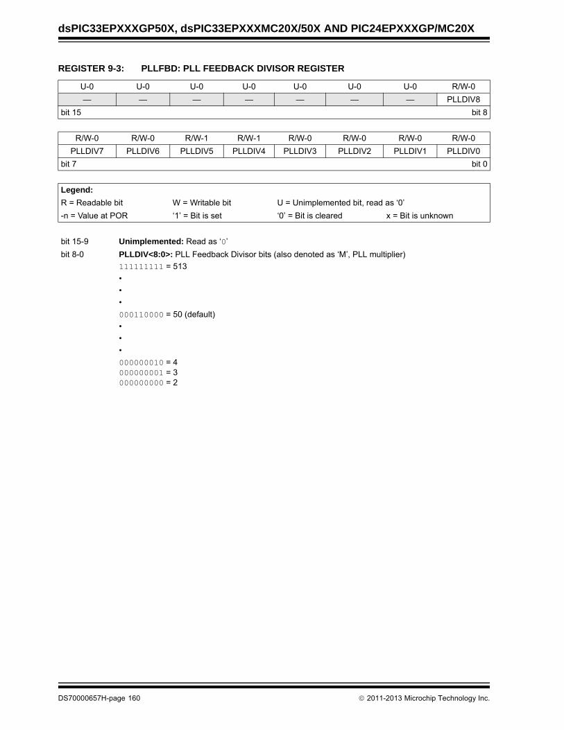
dsPIC33EPXXXGP50X, dsPIC33EPXXXMC20X/50X AND PIC24EPXXXGP/MC20X
REGISTER 9-3: PLLFBD: PLL FEEDBACK DIVISOR REGISTER
U-0 U-0 U-0 U-0 U-0 U-0 U-0 R/W-0
— — — — — — — PLLDIV8
bit 15 bit 8
R/W-0 R/W-0 R/W-1 R/W-1 R/W-0 R/W-0 R/W-0 R/W-0
PLLDIV7 PLLDIV6 PLLDIV5 PLLDIV4 PLLDIV3 PLLDIV2 PLLDIV1 PLLDIV0
bit 7 bit 0
Legend:
R = Readable bit W = Writable bit U = Unimplemented bit, read as ‘0’
-n = Value at POR ‘1’ = Bit is set ‘0’ = Bit is cleared x = Bit is unknown
bit 15-9 Unimplemented: Read as ‘0’
bit 8-0 PLLDIV<8:0>: PLL Feedback Divisor bits (also denoted as ‘M’, PLL multiplier)
111111111 = 513
•
•
•
000110000 = 50 (default)
•
•
•
000000010 = 4000000001 = 3000000000 = 2
DS70000657H-page 160 2011-2013 Microchip Technology Inc.
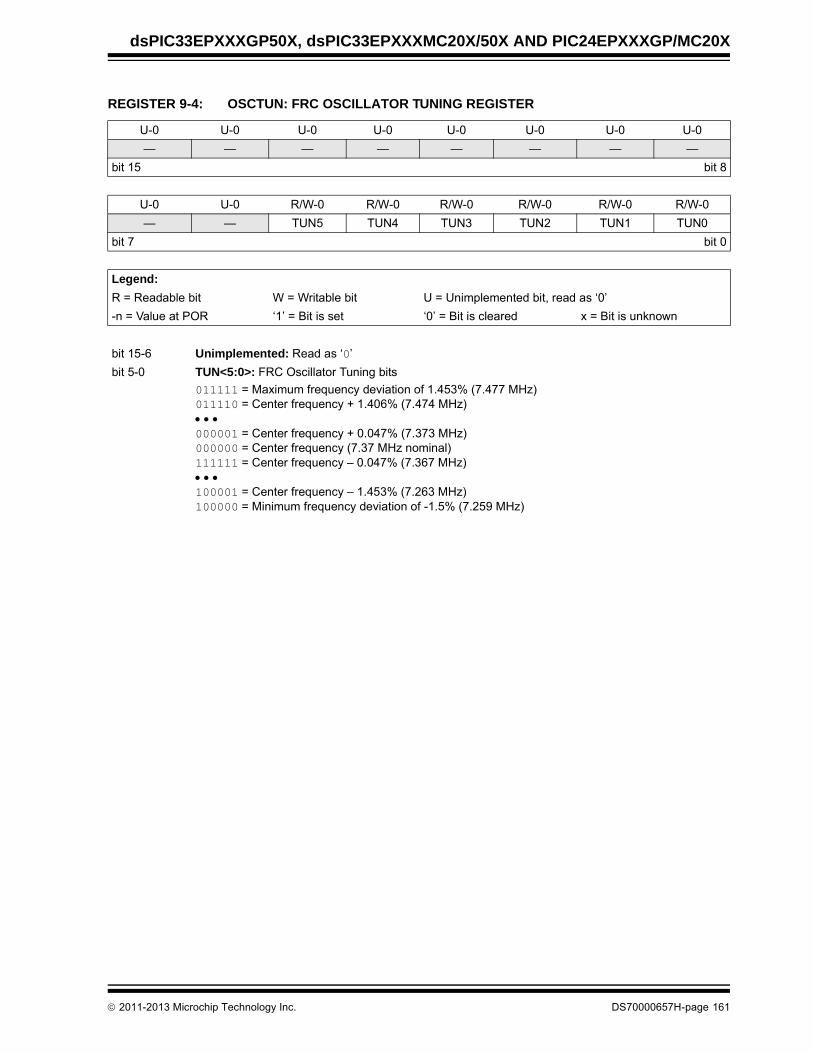
dsPIC33EPXXXGP50X, dsPIC33EPXXXMC20X/50X AND PIC24EPXXXGP/MC20X
REGISTER 9-4: OSCTUN: FRC OSCILLATOR TUNING REGISTER
U-0 U-0 U-0 U-0 U-0 U-0 U-0 U-0
— — — — — — — —
bit 15 bit 8
U-0 U-0 R/W-0 R/W-0 R/W-0 R/W-0 R/W-0 R/W-0
— — TUN5 TUN4 TUN3 TUN2 TUN1 TUN0
bit 7 bit 0
Legend:
R = Readable bit W = Writable bit U = Unimplemented bit, read as ‘0’
-n = Value at POR ‘1’ = Bit is set ‘0’ = Bit is cleared x = Bit is unknown
bit 15-6 Unimplemented: Read as ‘0’
bit 5-0 TUN<5:0>: FRC Oscillator Tuning bits
011111 = Maximum frequency deviation of 1.453% (7.477 MHz)011110 = Center frequency + 1.406% (7.474 MHz) 000001 = Center frequency + 0.047% (7.373 MHz)000000 = Center frequency (7.37 MHz nominal)111111 = Center frequency – 0.047% (7.367 MHz) 100001 = Center frequency – 1.453% (7.263 MHz)100000 = Minimum frequency deviation of -1.5% (7.259 MHz)
2011-2013 Microchip Technology Inc. DS70000657H-page 161

dsPIC33EPXXXGP50X, dsPIC33EPXXXMC20X/50X AND PIC24EPXXXGP/MC20X
REGISTER 9-5: REFOCON: REFERENCE OSCILLATOR CONTROL REGISTER
R/W-0 U-0 R/W-0 R/W-0 R/W-0 R/W-0 R/W-0 R/W-0
ROON — ROSSLP ROSEL RODIV3(1) RODIV2(1) RODIV1(1) RODIV0(1)
bit 15 bit 8
U-0 U-0 U-0 U-0 U-0 U-0 U-0 U-0
— — — — — — — —
bit 7 bit 0
Legend:
R = Readable bit W = Writable bit U = Unimplemented bit, read as ‘0’
-n = Value at POR ‘1’ = Bit is set ‘0’ = Bit is cleared x = Bit is unknown
bit 15 ROON: Reference Oscillator Output Enable bit
1 = Reference oscillator output is enabled on the REFCLK pin(2)
0 = Reference oscillator output is disabled
bit 14 Unimplemented: Read as ‘0’
bit 13 ROSSLP: Reference Oscillator Run in Sleep bit
1 = Reference oscillator output continues to run in Sleep0 = Reference oscillator output is disabled in Sleep
bit 12 ROSEL: Reference Oscillator Source Select bit
1 = Oscillator crystal is used as the reference clock0 = System clock is used as the reference clock
bit 11-8 RODIV<3:0>: Reference Oscillator Divider bits(1)
1111 = Reference clock divided by 32,7681110 = Reference clock divided by 16,3841101 = Reference clock divided by 8,1921100 = Reference clock divided by 4,0961011 = Reference clock divided by 2,0481010 = Reference clock divided by 1,0241001 = Reference clock divided by 5121000 = Reference clock divided by 2560111 = Reference clock divided by 1280110 = Reference clock divided by 640101 = Reference clock divided by 320100 = Reference clock divided by 160011 = Reference clock divided by 80010 = Reference clock divided by 40001 = Reference clock divided by 20000 = Reference clock
bit 7-0 Unimplemented: Read as ‘0’
Note 1: The reference oscillator output must be disabled (ROON = 0) before writing to these bits.
2: This pin is remappable. See Section 11.4 “Peripheral Pin Select (PPS)” for more information.
DS70000657H-page 162 2011-2013 Microchip Technology Inc.

dsPIC33EPXXXGP50X, dsPIC33EPXXXMC20X/50X AND PIC24EPXXXGP/MC20X
10.0 POWER-SAVING FEATURES
The dsPIC33EPXXXGP50X, dsPIC33EPXXXMC20X/50X and PIC24EPXXXGP/MC20X devices providethe ability to manage power consumption byselectively managing clocking to the CPU and theperipherals. In general, a lower clock frequency anda reduction in the number of peripherals beingclocked constitutes lower consumed power.
dsPIC33EPXXXGP50X, dsPIC33EPXXXMC20X/50Xand PIC24EPXXXGP/MC20X devices can managepower consumption in four ways:
• Clock Frequency
• Instruction-Based Sleep and Idle modes
• Software-Controlled Doze mode
• Selective Peripheral Control in Software
Combinations of these methods can be used to selec-tively tailor an application’s power consumption whilestill maintaining critical application features, such astiming-sensitive communications.
10.1 Clock Frequency and Clock Switching
The dsPIC33EPXXXGP50X, dsPIC33EPXXXMC20X/50X and PIC24EPXXXGP/MC20X devices allow awide range of clock frequencies to be selected underapplication control. If the system clock configuration isnot locked, users can choose low-power or high-precision oscillators by simply changing the NOSCxbits (OSCCON<10:8>). The process of changing asystem clock during operation, as well as limitations tothe process, are discussed in more detail inSection 9.0 “Oscillator Configuration”.
10.2 Instruction-Based Power-Saving Modes
The dsPIC33EPXXXGP50X, dsPIC33EPXXXMC20X/50X and PIC24EPXXXGP/MC20X devices have twospecial power-saving modes that are enteredthrough the execution of a special PWRSAVinstruction. Sleep mode stops clock operation andhalts all code execution. Idle mode halts the CPUand code execution, but allows peripheral modulesto continue operation. The assembler syntax of thePWRSAV instruction is shown in Example 10-1.
Sleep and Idle modes can be exited as a result of anenabled interrupt, WDT time-out or a device Reset. Whenthe device exits these modes, it is said to “wake-up”.
EXAMPLE 10-1: PWRSAV INSTRUCTION SYNTAX
Note 1: This data sheet summarizes thefeatures of the dsPIC33EPXXXGP50X,dsPIC33EPXXXMC20X/50X andPIC24EPXXXGP/MC20X families ofdevices. It is not intended to be a compre-hensive reference source. To complementthe information in this data sheet, refer to“Watchdog Timer and Power-SavingModes” (DS70615) in the “dsPIC33/PIC24 Family Reference Manual”, whichis available from the Microchip web site(www.microchip.com).
2: Some registers and associated bitsdescribed in this section may not beavailable on all devices. Refer toSection 4.0 “Memory Organization” inthis data sheet for device-specific registerand bit information.
Note: SLEEP_MODE and IDLE_MODE are con-stants defined in the assembler includefile for the selected device.
PWRSAV #SLEEP_MODE ; Put the device into Sleep modePWRSAV #IDLE_MODE ; Put the device into Idle mode
2011-2013 Microchip Technology Inc. DS70000657H-page 163

dsPIC33EPXXXGP50X, dsPIC33EPXXXMC20X/50X AND PIC24EPXXXGP/MC20X
10.2.1 SLEEP MODE
The following occurs in Sleep mode:
• The system clock source is shut down. If an on-chip oscillator is used, it is turned off.
• The device current consumption is reduced to a minimum, provided that no I/O pin is sourcing current.
• The Fail-Safe Clock Monitor does not operate, since the system clock source is disabled.
• The LPRC clock continues to run in Sleep mode if the WDT is enabled.
• The WDT, if enabled, is automatically cleared prior to entering Sleep mode.
• Some device features or peripherals can continue to operate. This includes items such as the Input Change Notification (ICN) on the I/O ports or peripherals that use an external clock input.
• Any peripheral that requires the system clock source for its operation is disabled.
The device wakes up from Sleep mode on any of theseevents:
• Any interrupt source that is individually enabled
• Any form of device Reset
• A WDT time-out
On wake-up from Sleep mode, the processor restartswith the same clock source that was active when Sleepmode was entered.
For optimal power savings, the internal regulator andthe Flash regulator can be configured to go intoStandby when Sleep mode is entered by clearing theVREGS (RCON<8>) and VREGSF (RCON<11>) bits(default configuration).
If the application requires a faster wake-up time, andcan accept higher current requirements, the VREGS(RCON<8>) and VREGSF (RCON<11>) bits can be setto keep the internal regulator and the Flash regulatoractive during Sleep mode.
10.2.2 IDLE MODE
The following occurs in Idle mode:
• The CPU stops executing instructions.• The WDT is automatically cleared.• The system clock source remains active. By
default, all peripheral modules continue to operate normally from the system clock source, but can also be selectively disabled (see Section 10.4 “Peripheral Module Disable”).
• If the WDT or FSCM is enabled, the LPRC also remains active.
The device wakes from Idle mode on any of theseevents:
• Any interrupt that is individually enabled
• Any device Reset
• A WDT time-out
On wake-up from Idle mode, the clock is reapplied tothe CPU and instruction execution will begin (2-4 clockcycles later), starting with the instruction following thePWRSAV instruction or the first instruction in theInterrupt Service Routine (ISR).
All peripherals also have the option to discontinueoperation when Idle mode is entered to allow forincreased power savings. This option is selectable inthe control register of each peripheral; for example, theTSIDL bit in the Timer1 Control register (T1CON<13>).
10.2.3 INTERRUPTS COINCIDENT WITH POWER SAVE INSTRUCTIONS
Any interrupt that coincides with the execution of aPWRSAV instruction is held off until entry into Sleep orIdle mode has completed. The device then wakes upfrom Sleep or Idle mode.
DS70000657H-page 164 2011-2013 Microchip Technology Inc.
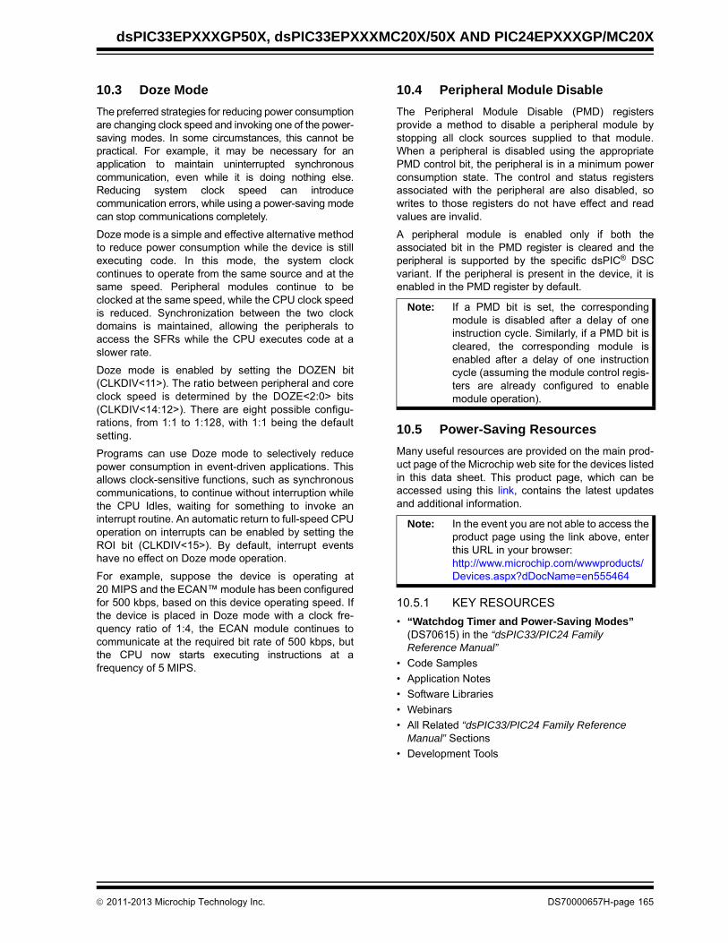
dsPIC33EPXXXGP50X, dsPIC33EPXXXMC20X/50X AND PIC24EPXXXGP/MC20X
10.3 Doze Mode
The preferred strategies for reducing power consumptionare changing clock speed and invoking one of the power-saving modes. In some circumstances, this cannot bepractical. For example, it may be necessary for anapplication to maintain uninterrupted synchronouscommunication, even while it is doing nothing else.Reducing system clock speed can introducecommunication errors, while using a power-saving modecan stop communications completely.
Doze mode is a simple and effective alternative methodto reduce power consumption while the device is stillexecuting code. In this mode, the system clockcontinues to operate from the same source and at thesame speed. Peripheral modules continue to beclocked at the same speed, while the CPU clock speedis reduced. Synchronization between the two clockdomains is maintained, allowing the peripherals toaccess the SFRs while the CPU executes code at aslower rate.
Doze mode is enabled by setting the DOZEN bit(CLKDIV<11>). The ratio between peripheral and coreclock speed is determined by the DOZE<2:0> bits(CLKDIV<14:12>). There are eight possible configu-rations, from 1:1 to 1:128, with 1:1 being the defaultsetting.
Programs can use Doze mode to selectively reducepower consumption in event-driven applications. Thisallows clock-sensitive functions, such as synchronouscommunications, to continue without interruption whilethe CPU Idles, waiting for something to invoke aninterrupt routine. An automatic return to full-speed CPUoperation on interrupts can be enabled by setting theROI bit (CLKDIV<15>). By default, interrupt eventshave no effect on Doze mode operation.
For example, suppose the device is operating at20 MIPS and the ECAN™ module has been configuredfor 500 kbps, based on this device operating speed. Ifthe device is placed in Doze mode with a clock fre-quency ratio of 1:4, the ECAN module continues tocommunicate at the required bit rate of 500 kbps, butthe CPU now starts executing instructions at afrequency of 5 MIPS.
10.4 Peripheral Module Disable
The Peripheral Module Disable (PMD) registersprovide a method to disable a peripheral module bystopping all clock sources supplied to that module.When a peripheral is disabled using the appropriatePMD control bit, the peripheral is in a minimum powerconsumption state. The control and status registersassociated with the peripheral are also disabled, sowrites to those registers do not have effect and readvalues are invalid.
A peripheral module is enabled only if both theassociated bit in the PMD register is cleared and theperipheral is supported by the specific dsPIC® DSCvariant. If the peripheral is present in the device, it isenabled in the PMD register by default.
10.5 Power-Saving Resources
Many useful resources are provided on the main prod-uct page of the Microchip web site for the devices listedin this data sheet. This product page, which can beaccessed using this link, contains the latest updatesand additional information.
10.5.1 KEY RESOURCES
• “Watchdog Timer and Power-Saving Modes” (DS70615) in the “dsPIC33/PIC24 Family Reference Manual”
• Code Samples
• Application Notes
• Software Libraries
• Webinars
• All Related “dsPIC33/PIC24 Family Reference Manual” Sections
• Development Tools
Note: If a PMD bit is set, the correspondingmodule is disabled after a delay of oneinstruction cycle. Similarly, if a PMD bit iscleared, the corresponding module isenabled after a delay of one instructioncycle (assuming the module control regis-ters are already configured to enablemodule operation).
Note: In the event you are not able to access theproduct page using the link above, enterthis URL in your browser:http://www.microchip.com/wwwproducts/Devices.aspx?dDocName=en555464
2011-2013 Microchip Technology Inc. DS70000657H-page 165

dsPIC33EPXXXGP50X, dsPIC33EPXXXMC20X/50X AND PIC24EPXXXGP/MC20X
REGISTER 10-1: PMD1: PERIPHERAL MODULE DISABLE CONTROL REGISTER 1
R/W-0 R/W-0 R/W-0 R/W-0 R/W-0 R/W-0 R/W-0 U-0
T5MD T4MD T3MD T2MD T1MD QEI1MD(1) PWMMD(1) —
bit 15 bit 8
R/W-0 R/W-0 R/W-0 R/W-0 R/W-0 U-0 R/W-0 R/W-0
I2C1MD U2MD U1MD SPI2MD SPI1MD — C1MD(2) AD1MD
bit 7 bit 0
Legend:
R = Readable bit W = Writable bit U = Unimplemented bit, read as ‘0’
-n = Value at POR ‘1’ = Bit is set ‘0’ = Bit is cleared x = Bit is unknown
bit 15 T5MD: Timer5 Module Disable bit1 = Timer5 module is disabled0 = Timer5 module is enabled
bit 14 T4MD: Timer4 Module Disable bit1 = Timer4 module is disabled0 = Timer4 module is enabled
bit 13 T3MD: Timer3 Module Disable bit1 = Timer3 module is disabled0 = Timer3 module is enabled
bit 12 T2MD: Timer2 Module Disable bit1 = Timer2 module is disabled0 = Timer2 module is enabled
bit 11 T1MD: Timer1 Module Disable bit1 = Timer1 module is disabled0 = Timer1 module is enabled
bit 10 QEI1MD: QEI1 Module Disable bit(1)
1 = QEI1 module is disabled0 = QEI1 module is enabled
bit 9 PWMMD: PWM Module Disable bit(1)
1 = PWM module is disabled0 = PWM module is enabled
bit 8 Unimplemented: Read as ‘0’
bit 7 I2C1MD: I2C1 Module Disable bit1 = I2C1 module is disabled0 = I2C1 module is enabled
bit 6 U2MD: UART2 Module Disable bit1 = UART2 module is disabled0 = UART2 module is enabled
bit 5 U1MD: UART1 Module Disable bit1 = UART1 module is disabled0 = UART1 module is enabled
bit 4 SPI2MD: SPI2 Module Disable bit1 = SPI2 module is disabled0 = SPI2 module is enabled
Note 1: This bit is available on dsPIC33EPXXXMC20X/50X and PIC24EPXXXMC20X devices only.
2: This bit is available on dsPIC33EPXXXGP50X and dsPIC33EPXXXMC50X devices only.
DS70000657H-page 166 2011-2013 Microchip Technology Inc.

dsPIC33EPXXXGP50X, dsPIC33EPXXXMC20X/50X AND PIC24EPXXXGP/MC20X
bit 3 SPI1MD: SPI1 Module Disable bit1 = SPI1 module is disabled0 = SPI1 module is enabled
bit 2 Unimplemented: Read as ‘0’
bit 1 C1MD: ECAN1 Module Disable bit(2)
1 = ECAN1 module is disabled0 = ECAN1 module is enabled
bit 0 AD1MD: ADC1 Module Disable bit1 = ADC1 module is disabled0 = ADC1 module is enabled
REGISTER 10-1: PMD1: PERIPHERAL MODULE DISABLE CONTROL REGISTER 1 (CONTINUED)
Note 1: This bit is available on dsPIC33EPXXXMC20X/50X and PIC24EPXXXMC20X devices only.
2: This bit is available on dsPIC33EPXXXGP50X and dsPIC33EPXXXMC50X devices only.
2011-2013 Microchip Technology Inc. DS70000657H-page 167

dsPIC33EPXXXGP50X, dsPIC33EPXXXMC20X/50X AND PIC24EPXXXGP/MC20X
REGISTER 10-2: PMD2: PERIPHERAL MODULE DISABLE CONTROL REGISTER 2
U-0 U-0 U-0 U-0 R/W-0 R/W-0 R/W-0 R/W-0
— — — — IC4MD IC3MD IC2MD IC1MD
bit 15 bit 8
U-0 U-0 U-0 U-0 R/W-0 R/W-0 R/W-0 R/W-0
— — — — OC4MD OC3MD OC2MD OC1MD
bit 7 bit 0
Legend:
R = Readable bit W = Writable bit U = Unimplemented bit, read as ‘0’
-n = Value at POR ‘1’ = Bit is set ‘0’ = Bit is cleared x = Bit is unknown
bit 15-12 Unimplemented: Read as ‘0’
bit 11 IC4MD: Input Capture 4 Module Disable bit
1 = Input Capture 4 module is disabled0 = Input Capture 4 module is enabled
bit 10 IC3MD: Input Capture 3 Module Disable bit
1 = Input Capture 3 module is disabled0 = Input Capture 3 module is enabled
bit 9 IC2MD: Input Capture 2 Module Disable bit
1 = Input Capture 2 module is disabled0 = Input Capture 2 module is enabled
bit 8 IC1MD: Input Capture 1 Module Disable bit
1 = Input Capture 1 module is disabled0 = Input Capture 1 module is enabled
bit 7-4 Unimplemented: Read as ‘0’
bit 3 OC4MD: Output Compare 4 Module Disable bit
1 = Output Compare 4 module is disabled0 = Output Compare 4 module is enabled
bit 2 OC3MD: Output Compare 3 Module Disable bit
1 = Output Compare 3 module is disabled0 = Output Compare 3 module is enabled
bit 1 OC2MD: Output Compare 2 Module Disable bit
1 = Output Compare 2 module is disabled0 = Output Compare 2 module is enabled
bit 0 OC1MD: Output Compare 1 Module Disable bit
1 = Output Compare 1 module is disabled0 = Output Compare 1 module is enabled
DS70000657H-page 168 2011-2013 Microchip Technology Inc.

dsPIC33EPXXXGP50X, dsPIC33EPXXXMC20X/50X AND PIC24EPXXXGP/MC20X
REGISTER 10-3: PMD3: PERIPHERAL MODULE DISABLE CONTROL REGISTER 3
REGISTER 10-4: PMD4: PERIPHERAL MODULE DISABLE CONTROL REGISTER 4
U-0 U-0 U-0 U-0 U-0 R/W-0 U-0 U-0
— — — — — CMPMD — —
bit 15 bit 8
R/W-0 U-0 U-0 U-0 U-0 U-0 R/W-0 U-0
CRCMD — — — — — I2C2MD —
bit 7 bit 0
Legend:
R = Readable bit W = Writable bit U = Unimplemented bit, read as ‘0’
-n = Value at POR ‘1’ = Bit is set ‘0’ = Bit is cleared x = Bit is unknown
bit 15-11 Unimplemented: Read as ‘0’
bit 10 CMPMD: Comparator Module Disable bit
1 = Comparator module is disabled0 = Comparator module is enabled
bit 9-8 Unimplemented: Read as ‘0’
bit 7 CRCMD: CRC Module Disable bit
1 = CRC module is disabled0 = CRC module is enabled
bit 6-2 Unimplemented: Read as ‘0’
bit 1 I2C2MD: I2C2 Module Disable bit
1 = I2C2 module is disabled0 = I2C2 module is enabled
bit 0 Unimplemented: Read as ‘0’
U-0 U-0 U-0 U-0 U-0 U-0 U-0 U-0
— — — — — — — —
bit 15 bit 8
U-0 U-0 U-0 U-0 R/W-0 R/W-0 U-0 U-0
— — — — REFOMD CTMUMD — —
bit 7 bit 0
Legend:
R = Readable bit W = Writable bit U = Unimplemented bit, read as ‘0’
-n = Value at POR ‘1’ = Bit is set ‘0’ = Bit is cleared x = Bit is unknown
bit 15-4 Unimplemented: Read as ‘0’
bit 3 REFOMD: Reference Clock Module Disable bit
1 = Reference clock module is disabled0 = Reference clock module is enabled
bit 2 CTMUMD: CTMU Module Disable bit
1 = CTMU module is disabled0 = CTMU module is enabled
bit 1-0 Unimplemented: Read as ‘0’
2011-2013 Microchip Technology Inc. DS70000657H-page 169

dsPIC33EPXXXGP50X, dsPIC33EPXXXMC20X/50X AND PIC24EPXXXGP/MC20X
REGISTER 10-5: PMD6: PERIPHERAL MODULE DISABLE CONTROL REGISTER 6
U-0 U-0 U-0 U-0 U-0 R/W-0 R/W-0 R/W-0
— — — — — PWM3MD(1) PWM2MD(1) PWM1MD(1)
bit 15 bit 8
U-0 U-0 U-0 U-0 U-0 U-0 U-0 U-0
— — — — — — — —
bit 7 bit 0
Legend:
R = Readable bit W = Writable bit U = Unimplemented bit, read as ‘0’
-n = Value at POR ‘1’ = Bit is set ‘0’ = Bit is cleared x = Bit is unknown
bit 15-11 Unimplemented: Read as ‘0’
bit 10 PWM3MD: PWM3 Module Disable bit(1)
1 = PWM3 module is disabled0 = PWM3 module is enabled
bit 9 PWM2MD: PWM2 Module Disable bit(1)
1 = PWM2 module is disabled0 = PWM2 module is enabled
bit 8 PWM1MD: PWM1 Module Disable bit(1)
1 = PWM1 module is disabled0 = PWM1 module is enabled
bit 7-0 Unimplemented: Read as ‘0’
Note 1: This bit is available on dsPIC33EPXXXMC50X/20X and PIC24EPXXXMC20X devices only.
DS70000657H-page 170 2011-2013 Microchip Technology Inc.
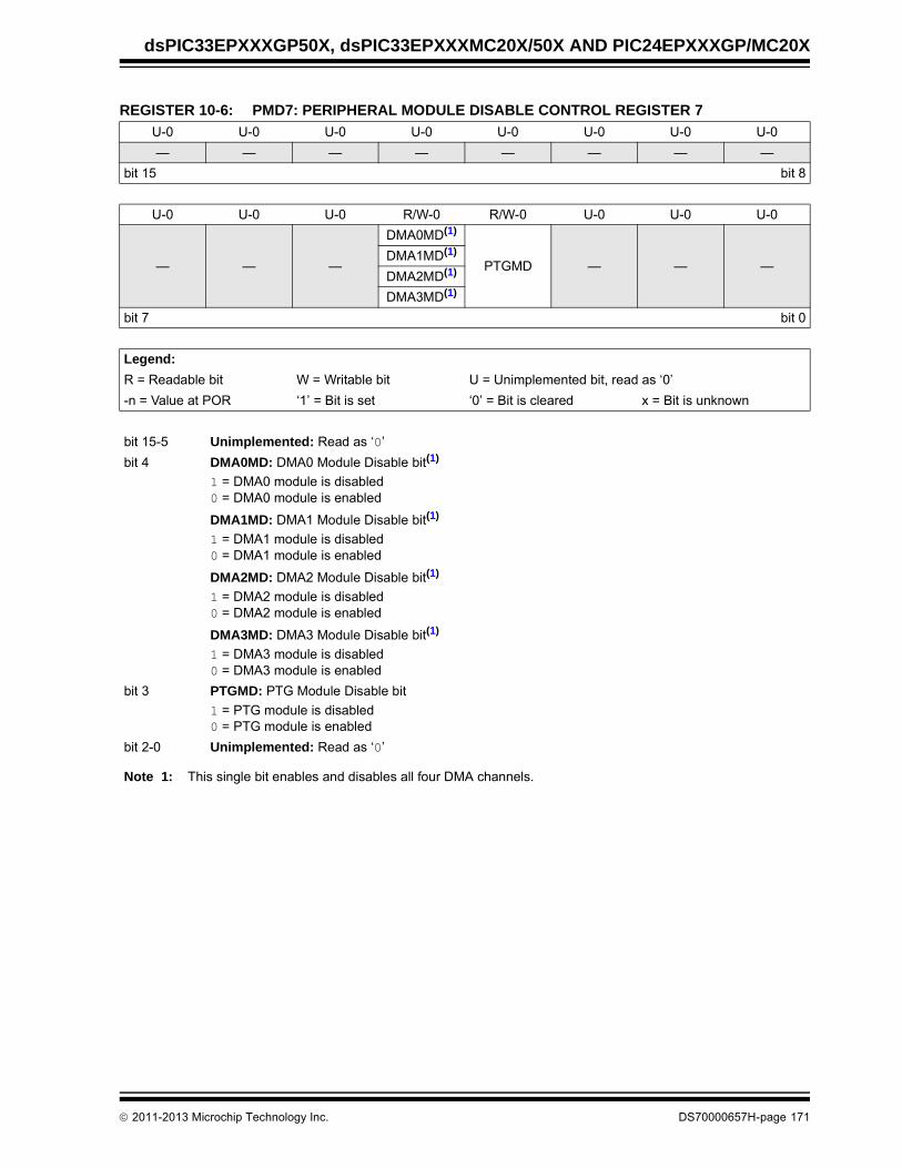
dsPIC33EPXXXGP50X, dsPIC33EPXXXMC20X/50X AND PIC24EPXXXGP/MC20X
REGISTER 10-6: PMD7: PERIPHERAL MODULE DISABLE CONTROL REGISTER 7
U-0 U-0 U-0 U-0 U-0 U-0 U-0 U-0
— — — — — — — —
bit 15 bit 8
U-0 U-0 U-0 R/W-0 R/W-0 U-0 U-0 U-0
— — —
DMA0MD(1)
PTGMD — — —DMA1MD(1)
DMA2MD(1)
DMA3MD(1)
bit 7 bit 0
Legend:
R = Readable bit W = Writable bit U = Unimplemented bit, read as ‘0’
-n = Value at POR ‘1’ = Bit is set ‘0’ = Bit is cleared x = Bit is unknown
bit 15-5 Unimplemented: Read as ‘0’
bit 4 DMA0MD: DMA0 Module Disable bit(1)
1 = DMA0 module is disabled0 = DMA0 module is enabled
DMA1MD: DMA1 Module Disable bit(1)
1 = DMA1 module is disabled0 = DMA1 module is enabled
DMA2MD: DMA2 Module Disable bit(1)
1 = DMA2 module is disabled0 = DMA2 module is enabled
DMA3MD: DMA3 Module Disable bit(1)
1 = DMA3 module is disabled0 = DMA3 module is enabled
bit 3 PTGMD: PTG Module Disable bit
1 = PTG module is disabled0 = PTG module is enabled
bit 2-0 Unimplemented: Read as ‘0’
Note 1: This single bit enables and disables all four DMA channels.
2011-2013 Microchip Technology Inc. DS70000657H-page 171

dsPIC33EPXXXGP50X, dsPIC33EPXXXMC20X/50X AND PIC24EPXXXGP/MC20X
NOTES:
DS70000657H-page 172 2011-2013 Microchip Technology Inc.

dsPIC33EPXXXGP50X, dsPIC33EPXXXMC20X/50X AND PIC24EPXXXGP/MC20X
11.0 I/O PORTS
Many of the device pins are shared among the peripher-als and the parallel I/O ports. All I/O input ports featureSchmitt Trigger inputs for improved noise immunity.
11.1 Parallel I/O (PIO) Ports
Generally, a parallel I/O port that shares a pin with aperipheral is subservient to the peripheral. Theperipheral’s output buffer data and control signals areprovided to a pair of multiplexers. The multiplexersselect whether the peripheral or the associated port
has ownership of the output data and control signals ofthe I/O pin. The logic also prevents “loop through,” inwhich a port’s digital output can drive the input of aperipheral that shares the same pin. Figure 11-1illustrates how ports are shared with other peripheralsand the associated I/O pin to which they are connected.
When a peripheral is enabled and the peripheral isactively driving an associated pin, the use of the pin as ageneral purpose output pin is disabled. The I/O pin canbe read, but the output driver for the parallel port bit isdisabled. If a peripheral is enabled, but the peripheral isnot actively driving a pin, that pin can be driven by a port.
All port pins have eight registers directly associated withtheir operation as digital I/O. The Data Direction register(TRISx) determines whether the pin is an input or an out-put. If the data direction bit is a ‘1’, then the pin is an input.All port pins are defined as inputs after a Reset. Readsfrom the Latch register (LATx) read the latch. Writes to theLatch write the latch. Reads from the port (PORTx) readthe port pins, while writes to the port pins write the latch.
Any bit and its associated data and control registersthat are not valid for a particular device is disabled.This means the corresponding LATx and TRISxregisters and the port pin are read as zeros.
When a pin is shared with another peripheral orfunction that is defined as an input only, it isnevertheless regarded as a dedicated port becausethere is no other competing source of outputs.
FIGURE 11-1: BLOCK DIAGRAM OF A TYPICAL SHARED PORT STRUCTURE
Note 1: This data sheet summarizes thefeatures of the dsPIC33EPXXXGP50X,dsPIC33EPXXXMC20X/50X andPIC24EPXXXGP/MC20X families ofdevices. It is not intended to be a compre-hensive reference source. To complementthe information in this data sheet, refer to“I/O Ports” (DS70598) in the “dsPIC33/PIC24 Family Reference Manual”, whichis available from the Microchip web site(www.microchip.com).
2: Some registers and associated bitsdescribed in this section may not beavailable on all devices. Refer toSection 4.0 “Memory Organization” inthis data sheet for device-specific registerand bit information.
QD
CK
WR LAT +
TRIS Latch
I/O Pin
WR Port
Data Bus
QD
CK
Data Latch
Read Port
Read TRIS
1
0
1
0
WR TRIS
Peripheral Output DataOutput Enable
Peripheral Input Data
I/O
Peripheral Module
Peripheral Output Enable
PIO Module
Output Multiplexers
Output Data
Input Data
Peripheral Module Enable
Read LAT
2011-2013 Microchip Technology Inc. DS70000657H-page 173
dsPIC33EPXXXGP50X, dsPIC33EPXXXMC20X/50X AND PIC24EPXXXGP/MC20X
11.1.1 OPEN-DRAIN CONFIGURATION
In addition to the PORTx, LATx and TRISx registersfor data control, port pins can also be individuallyconfigured for either digital or open-drain output. Thisis controlled by the Open-Drain Control register,ODCx, associated with each port. Setting any of thebits configures the corresponding pin to act as anopen-drain output.
The open-drain feature allows the generation ofoutputs other than VDD by using external pull-upresistors. The maximum open-drain voltage allowedon any pin is the same as the maximum VIH
specification for that particular pin.
See the “Pin Diagrams” section for the available5V tolerant pins and Table 30-11 for the maximumVIH specification for each pin.
11.2 Configuring Analog and Digital Port Pins
The ANSELx register controls the operation of theanalog port pins. The port pins that are to function asanalog inputs or outputs must have their correspondingANSELx and TRISx bits set. In order to use port pins forI/O functionality with digital modules, such as Timers,UARTs, etc., the corresponding ANSELx bit must becleared.
The ANSELx register has a default value of 0xFFFF;therefore, all pins that share analog functions areanalog (not digital) by default.
Pins with analog functions affected by the ANSELxregisters are listed with a buffer type of analog in thePinout I/O Descriptions (see Table 1-1).
If the TRISx bit is cleared (output) while the ANSELx bitis set, the digital output level (VOH or VOL) is convertedby an analog peripheral, such as the ADC module orcomparator module.
When the PORTx register is read, all pins configured asanalog input channels are read as cleared (a low level).
Pins configured as digital inputs do not convert ananalog input. Analog levels on any pin defined as adigital input (including the ANx pins) can cause theinput buffer to consume current that exceeds thedevice specifications.
11.2.1 I/O PORT WRITE/READ TIMING
One instruction cycle is required between a portdirection change or port write operation and a readoperation of the same port. Typically this instructionwould be a NOP, as shown in Example 11-1.
11.3 Input Change Notification (ICN)
The Input Change Notification function of the I/O portsallows devices to generate interrupt requests to theprocessor in response to a Change-of-State (COS) onselected input pins. This feature can detect inputChange-of-States even in Sleep mode, when the clocksare disabled. Every I/O port pin can be selected(enabled) for generating an interrupt request on aChange-of-State.
Three control registers are associated with the ChangeNotification (CN) functionality of each I/O port. TheCNENx registers contain the CN interrupt enable con-trol bits for each of the input pins. Setting any of thesebits enables a CN interrupt for the corresponding pins.
Each I/O pin also has a weak pull-up and a weakpull-down connected to it. The pull-ups and pull-downs act as a current source or sink sourceconnected to the pin and eliminate the need forexternal resistors when push button, or keypaddevices are connected. The pull-ups and pull-downsare enabled separately, using the CNPUx and theCNPDx registers, which contain the control bits foreach of the pins. Setting any of the control bitsenables the weak pull-ups and/or pull-downs for thecorresponding pins.
EXAMPLE 11-1: PORT WRITE/READ EXAMPLE
Note: Pull-ups and pull-downs on Change Noti-fication pins should always be disabledwhen the port pin is configured as a digitaloutput.
MOV 0xFF00, W0 ; Configure PORTB<15:8>; as inputs
MOV W0, TRISB ; and PORTB<7:0> ; as outputs
NOP ; Delay 1 cycleBTSS PORTB, #13 ; Next Instruction
DS70000657H-page 174 2011-2013 Microchip Technology Inc.

dsPIC33EPXXXGP50X, dsPIC33EPXXXMC20X/50X AND PIC24EPXXXGP/MC20X
11.4 Peripheral Pin Select (PPS)
A major challenge in general purpose devices is provid-ing the largest possible set of peripheral features whileminimizing the conflict of features on I/O pins. Thechallenge is even greater on low pin count devices. Inan application where more than one peripheral needsto be assigned to a single pin, inconvenient work-arounds in application code, or a complete redesign,may be the only option.
Peripheral Pin Select configuration provides analternative to these choices by enabling peripheral setselection and their placement on a wide range of I/Opins. By increasing the pinout options available on aparticular device, users can better tailor the device totheir entire application, rather than trimming theapplication to fit the device.
The Peripheral Pin Select configuration feature oper-ates over a fixed subset of digital I/O pins. Users mayindependently map the input and/or output of most dig-ital peripherals to any one of these I/O pins. Hardwaresafeguards are included that prevent accidental orspurious changes to the peripheral mapping once it hasbeen established.
11.4.1 AVAILABLE PINS
The number of available pins is dependent on theparticular device and its pin count. Pins that support thePeripheral Pin Select feature include the label, “RPn” or“RPIn”, in their full pin designation, where “n” is theremappable pin number. “RP” is used to designate pinsthat support both remappable input and outputfunctions, while “RPI” indicates pins that supportremappable input functions only.
11.4.2 AVAILABLE PERIPHERALS
The peripherals managed by the Peripheral Pin Selectare all digital-only peripherals. These include generalserial communications (UART and SPI), general pur-pose timer clock inputs, timer-related peripherals (inputcapture and output compare) and interrupt-on-changeinputs.
In comparison, some digital-only peripheral modulesare never included in the Peripheral Pin Select feature.This is because the peripheral’s function requiresspecial I/O circuitry on a specific port and cannot beeasily connected to multiple pins. These modulesinclude I2C™ and the PWM. A similar requirementexcludes all modules with analog inputs, such as theADC Converter.
A key difference between remappable and non-remappable peripherals is that remappable peripheralsare not associated with a default I/O pin. The peripheralmust always be assigned to a specific I/O pin before itcan be used. In contrast, non-remappable peripheralsare always available on a default pin, assuming that theperipheral is active and not conflicting with anotherperipheral.
When a remappable peripheral is active on a given I/Opin, it takes priority over all other digital I/O and digitalcommunication peripherals associated with the pin.Priority is given regardless of the type of peripheral thatis mapped. Remappable peripherals never take priorityover any analog functions associated with the pin.
11.4.3 CONTROLLING PERIPHERAL PIN SELECT
Peripheral Pin Select features are controlled throughtwo sets of SFRs: one to map peripheral inputs and oneto map outputs. Because they are separately con-trolled, a particular peripheral’s input and output (if theperipheral has both) can be placed on any selectablefunction pin without constraint.
The association of a peripheral to a peripheral-selectable pin is handled in two different ways,depending on whether an input or output is beingmapped.
2011-2013 Microchip Technology Inc. DS70000657H-page 175

dsPIC33EPXXXGP50X, dsPIC33EPXXXMC20X/50X AND PIC24EPXXXGP/MC20X
11.4.4 INPUT MAPPING
The inputs of the Peripheral Pin Select options aremapped on the basis of the peripheral. That is, a controlregister associated with a peripheral dictates the pin itwill be mapped to. The RPINRx registers are used toconfigure peripheral input mapping (see Register 11-1through Register 11-17). Each register contains sets of7-bit fields, with each set associated with one of theremappable peripherals. Programming a given periph-eral’s bit field with an appropriate 7-bit value maps theRPn pin with the corresponding value to that peripheral.For any given device, the valid range of values for anybit field corresponds to the maximum number ofPeripheral Pin Selections supported by the device.
For example, Figure 11-2 illustrates remappable pinselection for the U1RX input.
FIGURE 11-2: REMAPPABLE INPUT FOR U1RX
11.4.4.1 Virtual Connections
dsPIC33EPXXXGP50X, dsPIC33EPXXXMC20X/50Xand PIC24EPXXXGP/MC20X devices support virtual(internal) connections to the output of the op amp/comparator module (see Figure 25-1 in Section 25.0“Op Amp/Comparator Module”), and the PTGmodule (see Section 24.0 “Peripheral TriggerGenerator (PTG) Module”).
In addition, dsPIC33EPXXXMC20X/50X andPIC24EPXXXMC20X devices support virtual connec-tions to the filtered QEI module inputs: FINDX1,FHOME1, FINDX2 and FHOME2 (see Figure 17-1in Section 17.0 “Quadrature Encoder Interface(QEI) Module (dsPIC33EPXXXMC20X/50X andPIC24EPXXXMC20X Devices Only)”.
Virtual connections provide a simple way of inter-peripheral connection without utilizing a physical pin.For example, by setting the FLT1R<6:0> bits of theRPINR12 register to the value of ‘b0000001, theoutput of the analog comparator, C1OUT, will beconnected to the PWM Fault 1 input, which allows theanalog comparator to trigger PWM Faults without theuse of an actual physical pin on the device.
Virtual connection to the QEI module allowsperipherals to be connected to the QEI digital filterinput. To utilize this filter, the QEI module must beenabled and its inputs must be connected to a physicalRPn pin. Example 11-2 illustrates how the inputcapture module can be connected to the QEI digitalfilter.
EXAMPLE 11-2: CONNECTING IC1 TO THE HOME1 QEI1 DIGITAL FILTER INPUT ON PIN 43 OF THE dsPIC33EPXXXMC206 DEVICE
RP0
RP1
RP3
0
1
2U1RX Input
U1RXR<6:0>
to Peripheral
RPn
n
Note: For input only, Peripheral Pin Select func-tionality does not have priority over TRISxsettings. Therefore, when configuring anRPn pin for input, the corresponding bit inthe TRISx register must also be configuredfor input (set to ‘1’).
RPINR15 = 0x2500; /* Connect the QEI1 HOME1 input to RP37 (pin 43) */RPINR7 = 0x009; /* Connect the IC1 input to the digital filter on the FHOME1 input */
QEI1IOC = 0x4000; /* Enable the QEI digital filter */QEI1CON = 0x8000; /* Enable the QEI module */
DS70000657H-page 176 2011-2013 Microchip Technology Inc.

dsPIC33EPXXXGP50X, dsPIC33EPXXXMC20X/50X AND PIC24EPXXXGP/MC20X
TABLE 11-1: SELECTABLE INPUT SOURCES (MAPS INPUT TO FUNCTION)
Input Name(1) Function Name Register Configuration Bits
External Interrupt 1 INT1 RPINR0 INT1R<6:0>
External Interrupt 2 INT2 RPINR1 INT2R<6:0>
Timer2 External Clock T2CK RPINR3 T2CKR<6:0>
Input Capture 1 IC1 RPINR7 IC1R<6:0>
Input Capture 2 IC2 RPINR7 IC2R<6:0>
Input Capture 3 IC3 RPINR8 IC3R<6:0>
Input Capture 4 IC4 RPINR8 IC4R<6:0>
Output Compare Fault A OCFA RPINR11 OCFAR<6:0>
PWM Fault 1(3) FLT1 RPINR12 FLT1R<6:0>
PWM Fault 2(3) FLT2 RPINR12 FLT2R<6:0>
QEI1 Phase A(3) QEA1 RPINR14 QEA1R<6:0>
QEI1 Phase B(3) QEB1 RPINR14 QEB1R<6:0>
QEI1 Index(3) INDX1 RPINR15 INDX1R<6:0>
QEI1 Home(3) HOME1 RPINR15 HOM1R<6:0>
UART1 Receive U1RX RPINR18 U1RXR<6:0>
UART2 Receive U2RX RPINR19 U2RXR<6:0>
SPI2 Data Input SDI2 RPINR22 SDI2R<6:0>
SPI2 Clock Input SCK2 RPINR22 SCK2R<6:0>
SPI2 Slave Select SS2 RPINR23 SS2R<6:0>
CAN1 Receive(2) C1RX RPINR26 C1RXR<6:0>
PWM Sync Input 1(3) SYNCI1 RPINR37 SYNCI1R<6:0>
PWM Dead-Time Compensation 1(3) DTCMP1 RPINR38 DTCMP1R<6:0>
PWM Dead-Time Compensation 2(3) DTCMP2 RPINR39 DTCMP2R<6:0>
PWM Dead-Time Compensation 3(3) DTCMP3 RPINR39 DTCMP3R<6:0>
Note 1: Unless otherwise noted, all inputs use the Schmitt Trigger input buffers.
2: This input source is available on dsPIC33EPXXXGP/MC50X devices only.
3: This input source is available on dsPIC33EPXXXMC20X/50X and PIC24EPXXXMC20X devices only.
2011-2013 Microchip Technology Inc. DS70000657H-page 177

dsPIC33EPXXXGP50X, dsPIC33EPXXXMC20X/50X AND PIC24EPXXXGP/MC20X
TABLE 11-2: INPUT PIN SELECTION FOR SELECTABLE INPUT SOURCES
Peripheral Pin Select Input
Register Value
Input/Output
Pin AssignmentPeripheral Pin Select Input
Register Value
Input/Output
Pin Assignment
000 0000 I VSS 010 1101 I RPI45
000 0001 I C1OUT(1) 010 1110 I RPI46
000 0010 I C2OUT(1) 010 1111 I RPI47
000 0011 I C3OUT(1) 011 0000 — —
000 0100 I C4OUT(1) 011 0001 — —
000 0101 — — 011 0010 — —
000 0110 I PTGO30(1) 011 0011 I RPI51
000 0111 I PTGO31(1) 011 0100 I RPI52
000 1000 I FINDX1(1,2) 011 0101 I RPI53
000 1001 I FHOME1(1,2) 011 0110 I/O RP54
000 1010 — — 011 0111 I/O RP55
000 1011 — — 011 1000 I/O RP56
000 1100 — — 011 1001 I/O RP57
000 1101 — — 011 1010 I RPI58
000 1110 — — 011 1011 — —
000 1111 — — 011 1100 — —
001 0000 — — 011 1101 — —
001 0001 — — 011 1110 — —
001 0010 — — 011 1111 — —
001 0011 — — 100 0000 — —
001 0100 I/O RP20 100 0001 — —
001 0101 — — 100 0010 — —
001 0110 — — 100 0011 — —
001 0111 — — 100 0100 — —
001 1000 I RPI24 100 0101 — —
001 1001 I RPI25 100 0110 — —
001 1010 — — 100 0111 — —
001 1011 I RPI27 100 1000 — —
001 1100 I RPI28 100 1001 — —
001 1101 — — 100 1010 — —
001 1110 — — 100 1011 — —
001 1111 — — 100 1100 — —
010 0000 I RPI32 100 1101 — —
010 0001 I RPI33 100 1110 — —
010 0010 I RPI34 100 1111 — —
010 0011 I/O RP35 101 0000 — —
010 0100 I/O RP36 101 0001 — —
010 0101 I/O RP37 101 0010 — —
010 0110 I/O RP38 101 0011 — —
010 0111 I/O RP39 101 0100 — —
Legend: Shaded rows indicate PPS Input register values that are unimplemented.
Note 1: See Section 11.4.4.1 “Virtual Connections” for more information on selecting this pin assignment.
2: These inputs are available on dsPIC33EPXXXGP/MC50X devices only.
DS70000657H-page 178 2011-2013 Microchip Technology Inc.
dsPIC33EPXXXGP50X, dsPIC33EPXXXMC20X/50X AND PIC24EPXXXGP/MC20X
010 1000 I/O RP40 101 0101 — —
010 1001 I/O RP41 101 0110 — —
010 1010 I/O RP42 101 0111 — —
010 1011 I/O RP43 101 1000 — —
010 1100 I RPI44 101 1001 — —
101 1010 — — 110 1101 — —
101 1011 — — 110 1110 — —
101 1100 — — 110 1111 — —
101 1101 — — 111 0000 — —
101 1110 I RPI94 111 0001 — —
101 1111 I RPI95 111 0010 — —
110 0000 I RPI96 111 0011 — —
110 0001 I/O RP97 111 0100 — —
110 0010 — — 111 0101 — —
110 0011 — — 111 0110 I/O RP118
110 0100 — — 111 0111 I RPI119
110 0101 — — 111 1000 I/O RP120
110 0110 — — 111 1001 I RPI121
110 0111 — — 111 1010 — —
110 1000 — — 111 1011 — —
110 1001 — — 111 1100 — —
110 1010 — — 111 1101 — —
110 1011 — — 111 1110 — —
110 1100 — — 111 1111 — —
TABLE 11-2: INPUT PIN SELECTION FOR SELECTABLE INPUT SOURCES (CONTINUED)
Peripheral Pin Select Input
Register Value
Input/Output
Pin AssignmentPeripheral Pin Select Input
Register Value
Input/Output
Pin Assignment
Legend: Shaded rows indicate PPS Input register values that are unimplemented.
Note 1: See Section 11.4.4.1 “Virtual Connections” for more information on selecting this pin assignment.
2: These inputs are available on dsPIC33EPXXXGP/MC50X devices only.
2011-2013 Microchip Technology Inc. DS70000657H-page 179
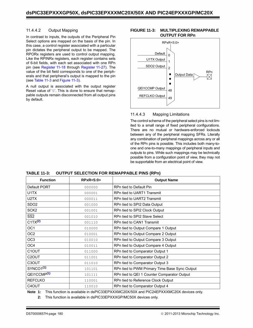
dsPIC33EPXXXGP50X, dsPIC33EPXXXMC20X/50X AND PIC24EPXXXGP/MC20X
11.4.4.2 Output Mapping
In contrast to inputs, the outputs of the Peripheral PinSelect options are mapped on the basis of the pin. Inthis case, a control register associated with a particularpin dictates the peripheral output to be mapped. TheRPORx registers are used to control output mapping.Like the RPINRx registers, each register contains setsof 6-bit fields, with each set associated with one RPnpin (see Register 11-18 through Register 11-27). Thevalue of the bit field corresponds to one of the periph-erals and that peripheral’s output is mapped to the pin(see Table 11-3 and Figure 11-3).
A null output is associated with the output registerReset value of ‘0’. This is done to ensure that remap-pable outputs remain disconnected from all output pinsby default.
FIGURE 11-3: MULTIPLEXING REMAPPABLE OUTPUT FOR RPn
11.4.4.3 Mapping Limitations
The control schema of the peripheral select pins is not lim-ited to a small range of fixed peripheral configurations.There are no mutual or hardware-enforced lockoutsbetween any of the peripheral mapping SFRs. Literallyany combination of peripheral mappings across any or allof the RPn pins is possible. This includes both many-to-one and one-to-many mappings of peripheral inputs andoutputs to pins. While such mappings may be technicallypossible from a configuration point of view, they may notbe supportable from an electrical point of view.
RPxR<5:0>
0
49
1
Default
U1TX Output
SDO2 Output2
REFCLKO Output
48QEI1CCMP Output
Output DataRPn
TABLE 11-3: OUTPUT SELECTION FOR REMAPPABLE PINS (RPn)
Function RPxR<5:0> Output Name
Default PORT 000000 RPn tied to Default Pin
U1TX 000001 RPn tied to UART1 Transmit
U2TX 000011 RPn tied to UART2 Transmit
SDO2 001000 RPn tied to SPI2 Data Output
SCK2 001001 RPn tied to SPI2 Clock Output
SS2 001010 RPn tied to SPI2 Slave Select
C1TX(2) 001110 RPn tied to CAN1 Transmit
OC1 010000 RPn tied to Output Compare 1 Output
OC2 010001 RPn tied to Output Compare 2 Output
OC3 010010 RPn tied to Output Compare 3 Output
OC4 010011 RPn tied to Output Compare 4 Output
C1OUT 011000 RPn tied to Comparator Output 1
C2OUT 011001 RPn tied to Comparator Output 2
C3OUT 011010 RPn tied to Comparator Output 3
SYNCO1(1) 101101 RPn tied to PWM Primary Time Base Sync Output
QEI1CCMP(1) 101111 RPn tied to QEI 1 Counter Comparator Output
REFCLKO 110001 RPn tied to Reference Clock Output
C4OUT 110010 RPn tied to Comparator Output 4
Note 1: This function is available in dsPIC33EPXXXMC20X/50X and PIC24EPXXXMC20X devices only.
2: This function is available in dsPIC33EPXXXGP/MC50X devices only.
DS70000657H-page 180 2011-2013 Microchip Technology Inc.

dsPIC33EPXXXGP50X, dsPIC33EPXXXMC20X/50X AND PIC24EPXXXGP/MC20X
11.5 I/O Helpful Tips
1. In some cases, certain pins, as defined inTable 30-11, under “Injection Current”, have inter-nal protection diodes to VDD and VSS. The term,“Injection Current”, is also referred to as “ClampCurrent”. On designated pins, with sufficient exter-nal current-limiting precautions by the user, I/O pininput voltages are allowed to be greater or lessthan the data sheet absolute maximum ratings,with respect to the VSS and VDD supplies. Notethat when the user application forward biaseseither of the high or low side internal input clampdiodes, that the resulting current being injectedinto the device, that is clamped internally by theVDD and VSS power rails, may affect the ADCaccuracy by four to six counts.
2. I/O pins that are shared with any analog input pin(i.e., ANx) are always analog pins by default afterany Reset. Consequently, configuring a pin as ananalog input pin automatically disables the digitalinput pin buffer and any attempt to read the digitalinput level by reading PORTx or LATx will alwaysreturn a ‘0’, regardless of the digital logic level onthe pin. To use a pin as a digital I/O pin on a sharedANx pin, the user application needs to configure theAnalog Pin Configuration registers in the I/O portsmodule (i.e., ANSELx) by setting the appropriate bitthat corresponds to that I/O port pin to a ‘0’.
3. Most I/O pins have multiple functions. Referring tothe device pin diagrams in this data sheet, the prior-ities of the functions allocated to any pins areindicated by reading the pin name from left-to-right.The left most function name takes precedence overany function to its right in the naming convention.For example: AN16/T2CK/T7CK/RC1. This indi-cates that AN16 is the highest priority in thisexample and will supersede all other functions to itsright in the list. Those other functions to its right,even if enabled, would not work as long as anyother function to its left was enabled. This ruleapplies to all of the functions listed for a given pin.
4. Each pin has an internal weak pull-up resistor andpull-down resistor that can be configured using theCNPUx and CNPDx registers, respectively. Theseresistors eliminate the need for external resistorsin certain applications. The internal pull-up is up to~(VDD – 0.8), not VDD. This value is still above theminimum VIH of CMOS and TTL devices.
5. When driving LEDs directly, the I/O pin can sourceor sink more current than what is specified in theVOH/IOH and VOL/IOL DC characteristic specifica-tion. The respective IOH and IOL current rating onlyapplies to maintaining the corresponding output ator above the VOH, and at or below the VOL levels.However, for LEDs, unlike digital inputs of anexternally connected device, they are not gov-erned by the same minimum VIH/VIL levels. An I/Opin output can safely sink or source any currentless than that listed in the absolute maximumrating section of this data sheet. For example:
VOH = 2.4V @ IOH = -8 mA and VDD = 3.3V
The maximum output current sourced by any 8 mA I/O pin = 12 mA.
LED source current < 12 mA is technicallypermitted. Refer to the VOH/IOH graphs inSection 30.0 “Electrical Characteristics” foradditional information.
6. The Peripheral Pin Select (PPS) pin mapping rulesare as follows:
a) Only one “output” function can be active on agiven pin at any time, regardless if it is a ded-icated or remappable function (one pin, oneoutput).
b) It is possible to assign a “remappable output”function to multiple pins and externally short ortie them together for increased current drive.
c) If any “dedicated output” function is enabledon a pin, it will take precedence over anyremappable “output” function.
d) If any “dedicated digital” (input or output) func-tion is enabled on a pin, any number of “input”remappable functions can be mapped to thesame pin.
e) If any “dedicated analog” function(s) areenabled on a given pin, “digital input(s)” of anykind will all be disabled, although a single “dig-ital output”, at the user’s cautionary discretion,can be enabled and active as long as there isno signal contention with an external analoginput signal. For example, it is possible for theADC to convert the digital output logic level, orto toggle a digital output on a comparator orADC input provided there is no externalanalog input, such as for a built-in self-test.
f) Any number of “input” remappable functionscan be mapped to the same pin(s) at the sametime, including to any pin with a single outputfrom either a dedicated or remappable “output”.
Note: Although it is not possible to use a digitalinput pin when its analog function isenabled, it is possible to use the digital I/Ooutput function, TRISx = 0x0, while theanalog function is also enabled. However,this is not recommended, particularly if theanalog input is connected to an externalanalog voltage source, which wouldcreate signal contention between theanalog signal and the output pin driver.
2011-2013 Microchip Technology Inc. DS70000657H-page 181
dsPIC33EPXXXGP50X, dsPIC33EPXXXMC20X/50X AND PIC24EPXXXGP/MC20X
g) The TRISx registers control only the digital I/Ooutput buffer. Any other dedicated or remappa-ble active “output” will automatically overridethe TRIS setting. The TRISx register does notcontrol the digital logic “input” buffer. Remap-pable digital “inputs” do not automaticallyoverride TRIS settings, which means that theTRISx bit must be set to input for pins with onlyremappable input function(s) assigned
h) All analog pins are enabled by default after anyReset and the corresponding digital inputbuffer on the pin has been disabled. Only theAnalog Pin Select registers control the digitalinput buffer, not the TRISx register. The usermust disable the analog function on a pin usingthe Analog Pin Select registers in order to useany “digital input(s)” on a corresponding pin, noexceptions.
11.6 I/O Ports Resources
Many useful resources are provided on the main prod-uct page of the Microchip web site for the devices listedin this data sheet. This product page, which can beaccessed using this link, contains the latest updatesand additional information.
11.6.1 KEY RESOURCES
• “I/O Ports” (DS70598) in the “dsPIC33/PIC24 Family Reference Manual”
• Code Samples
• Application Notes
• Software Libraries
• Webinars
• All Related “dsPIC33/PIC24 Family Reference Manual” Sections
• Development Tools
Note: In the event you are not able to access theproduct page using the link above, enterthis URL in your browser:http://www.microchip.com/wwwproducts/Devices.aspx?dDocName=en555464
DS70000657H-page 182 2011-2013 Microchip Technology Inc.
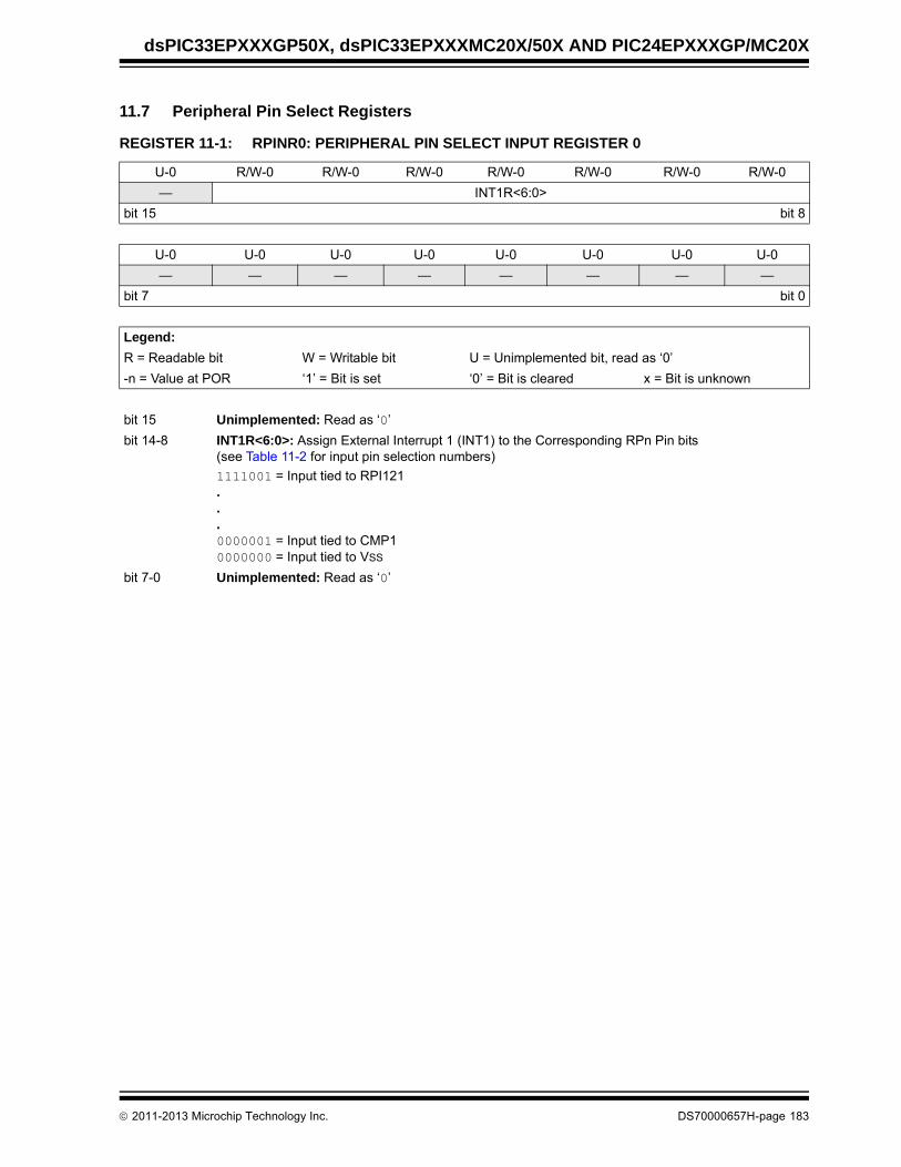
dsPIC33EPXXXGP50X, dsPIC33EPXXXMC20X/50X AND PIC24EPXXXGP/MC20X
11.7 Peripheral Pin Select Registers
REGISTER 11-1: RPINR0: PERIPHERAL PIN SELECT INPUT REGISTER 0
U-0 R/W-0 R/W-0 R/W-0 R/W-0 R/W-0 R/W-0 R/W-0
— INT1R<6:0>
bit 15 bit 8
U-0 U-0 U-0 U-0 U-0 U-0 U-0 U-0
— — — — — — — —
bit 7 bit 0
Legend:
R = Readable bit W = Writable bit U = Unimplemented bit, read as ‘0’
-n = Value at POR ‘1’ = Bit is set ‘0’ = Bit is cleared x = Bit is unknown
bit 15 Unimplemented: Read as ‘0’
bit 14-8 INT1R<6:0>: Assign External Interrupt 1 (INT1) to the Corresponding RPn Pin bits(see Table 11-2 for input pin selection numbers)
1111001 = Input tied to RPI121...0000001 = Input tied to CMP10000000 = Input tied to VSS
bit 7-0 Unimplemented: Read as ‘0’
2011-2013 Microchip Technology Inc. DS70000657H-page 183
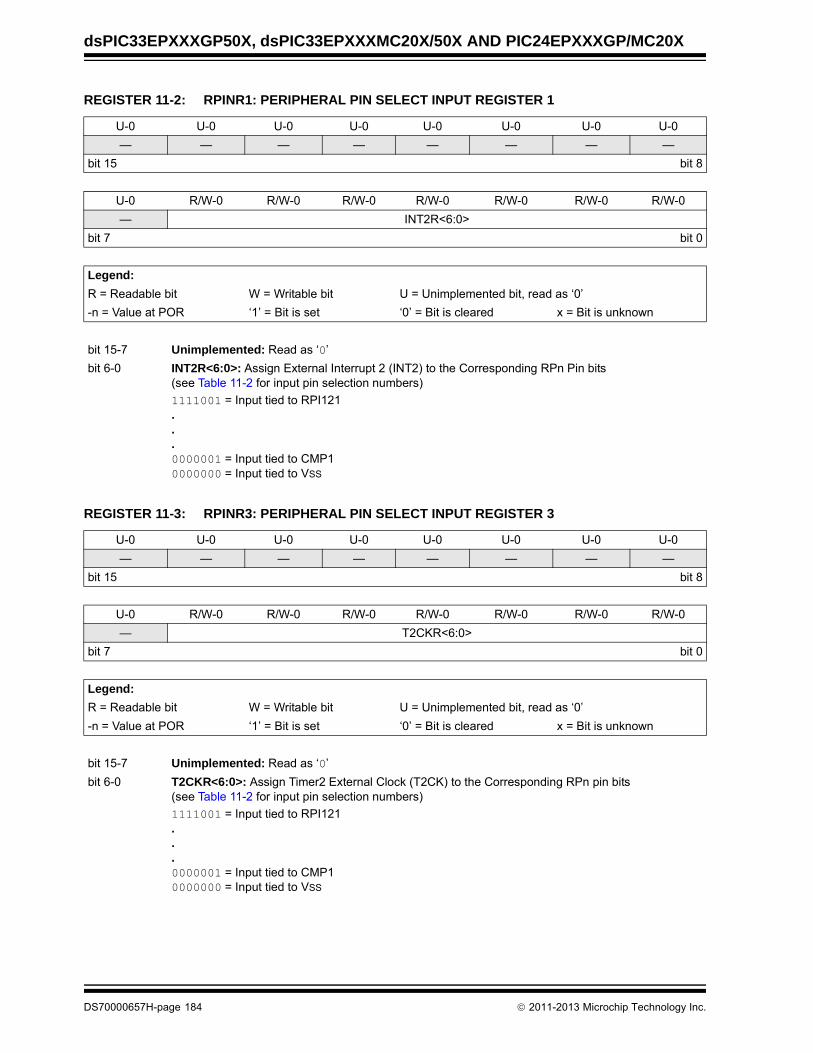
dsPIC33EPXXXGP50X, dsPIC33EPXXXMC20X/50X AND PIC24EPXXXGP/MC20X
REGISTER 11-2: RPINR1: PERIPHERAL PIN SELECT INPUT REGISTER 1
U-0 U-0 U-0 U-0 U-0 U-0 U-0 U-0
— — — — — — — —
bit 15 bit 8
U-0 R/W-0 R/W-0 R/W-0 R/W-0 R/W-0 R/W-0 R/W-0
— INT2R<6:0>
bit 7 bit 0
Legend:
R = Readable bit W = Writable bit U = Unimplemented bit, read as ‘0’
-n = Value at POR ‘1’ = Bit is set ‘0’ = Bit is cleared x = Bit is unknown
bit 15-7 Unimplemented: Read as ‘0’
bit 6-0 INT2R<6:0>: Assign External Interrupt 2 (INT2) to the Corresponding RPn Pin bits(see Table 11-2 for input pin selection numbers)
1111001 = Input tied to RPI121...0000001 = Input tied to CMP10000000 = Input tied to VSS
REGISTER 11-3: RPINR3: PERIPHERAL PIN SELECT INPUT REGISTER 3
U-0 U-0 U-0 U-0 U-0 U-0 U-0 U-0
— — — — — — — —
bit 15 bit 8
U-0 R/W-0 R/W-0 R/W-0 R/W-0 R/W-0 R/W-0 R/W-0
— T2CKR<6:0>
bit 7 bit 0
Legend:
R = Readable bit W = Writable bit U = Unimplemented bit, read as ‘0’
-n = Value at POR ‘1’ = Bit is set ‘0’ = Bit is cleared x = Bit is unknown
bit 15-7 Unimplemented: Read as ‘0’
bit 6-0 T2CKR<6:0>: Assign Timer2 External Clock (T2CK) to the Corresponding RPn pin bits(see Table 11-2 for input pin selection numbers)
1111001 = Input tied to RPI121...0000001 = Input tied to CMP10000000 = Input tied to VSS
DS70000657H-page 184 2011-2013 Microchip Technology Inc.

dsPIC33EPXXXGP50X, dsPIC33EPXXXMC20X/50X AND PIC24EPXXXGP/MC20X
REGISTER 11-4: RPINR7: PERIPHERAL PIN SELECT INPUT REGISTER 7
U-0 R/W-0 R/W-0 R/W-0 R/W-0 R/W-0 R/W-0 R/W-0
— IC2R<6:0>
bit 15 bit 8
U-0 R/W-0 R/W-0 R/W-0 R/W-0 R/W-0 R/W-0 R/W-0
— IC1R<6:0>
bit 7 bit 0
Legend:
R = Readable bit W = Writable bit U = Unimplemented bit, read as ‘0’
-n = Value at POR ‘1’ = Bit is set ‘0’ = Bit is cleared x = Bit is unknown
bit 15 Unimplemented: Read as ‘0’
bit 14-8 IC2R<6:0>: Assign Input Capture 2 (IC2) to the Corresponding RPn Pin bits(see Table 11-2 for input pin selection numbers)
1111001 = Input tied to RPI121...0000001 = Input tied to CMP10000000 = Input tied to VSS
bit 7 Unimplemented: Read as ‘0’
bit 6-0 IC1R<6:0>: Assign Input Capture 1 (IC1) to the Corresponding RPn Pin bits(see Table 11-2 for input pin selection numbers)
1111001 = Input tied to RPI121...0000001 = Input tied to CMP10000000 = Input tied to VSS
2011-2013 Microchip Technology Inc. DS70000657H-page 185

dsPIC33EPXXXGP50X, dsPIC33EPXXXMC20X/50X AND PIC24EPXXXGP/MC20X
REGISTER 11-5: RPINR8: PERIPHERAL PIN SELECT INPUT REGISTER 8
U-0 R/W-0 R/W-0 R/W-0 R/W-0 R/W-0 R/W-0 R/W-0
— IC4R<6:0>
bit 15 bit 8
U-0 R/W-0 R/W-0 R/W-0 R/W-0 R/W-0 R/W-0 R/W-0
— IC3R<6:0>
bit 7 bit 0
Legend:
R = Readable bit W = Writable bit U = Unimplemented bit, read as ‘0’
-n = Value at POR ‘1’ = Bit is set ‘0’ = Bit is cleared x = Bit is unknown
bit 15 Unimplemented: Read as ‘0’
bit 14-8 IC4R<6:0>: Assign Input Capture 4 (IC4) to the Corresponding RPn Pin bits(see Table 11-2 for input pin selection numbers)
1111001 = Input tied to RPI121...0000001 = Input tied to CMP10000000 = Input tied to VSS
bit 7 Unimplemented: Read as ‘0’
bit 6-0 IC3R<6:0>: Assign Input Capture 3 (IC3) to the Corresponding RPn Pin bits(see Table 11-2 for input pin selection numbers)
1111001 = Input tied to RPI121...0000001 = Input tied to CMP10000000 = Input tied to VSS
DS70000657H-page 186 2011-2013 Microchip Technology Inc.

dsPIC33EPXXXGP50X, dsPIC33EPXXXMC20X/50X AND PIC24EPXXXGP/MC20X
REGISTER 11-6: RPINR11: PERIPHERAL PIN SELECT INPUT REGISTER 11
U-0 U-0 U-0 U-0 U-0 U-0 U-0 U-0
— — — — — — — —
bit 15 bit 8
U-0 R/W-0 R/W-0 R/W-0 R/W-0 R/W-0 R/W-0 R/W-0
— OCFAR<6:0>
bit 7 bit 0
Legend:
R = Readable bit W = Writable bit U = Unimplemented bit, read as ‘0’
-n = Value at POR ‘1’ = Bit is set ‘0’ = Bit is cleared x = Bit is unknown
bit 15-7 Unimplemented: Read as ‘0’
bit 6-0 OCFAR<6:0>: Assign Output Compare Fault A (OCFA) to the Corresponding RPn Pin bits(see Table 11-2 for input pin selection numbers)
1111001 = Input tied to RPI121...0000001 = Input tied to CMP10000000 = Input tied to VSS
2011-2013 Microchip Technology Inc. DS70000657H-page 187

dsPIC33EPXXXGP50X, dsPIC33EPXXXMC20X/50X AND PIC24EPXXXGP/MC20X
REGISTER 11-7: RPINR12: PERIPHERAL PIN SELECT INPUT REGISTER 12 (dsPIC33EPXXXMC20X/50X and PIC24EPXXXMC20X DEVICES ONLY)
U-0 R/W-0 R/W-0 R/W-0 R/W-0 R/W-0 R/W-0 R/W-0
— FLT2R<6:0>
bit 15 bit 8
U-0 R/W-0 R/W-0 R/W-0 R/W-0 R/W-0 R/W-0 R/W-0
— FLT1R<6:0>
bit 7 bit 0
Legend:
R = Readable bit W = Writable bit U = Unimplemented bit, read as ‘0’
-n = Value at POR ‘1’ = Bit is set ‘0’ = Bit is cleared x = Bit is unknown
bit 15 Unimplemented: Read as ‘0’
bit 14-8 FLT2R<6:0>: Assign PWM Fault 2 (FLT2) to the Corresponding RPn Pin bits(see Table 11-2 for input pin selection numbers)
1111001 = Input tied to RPI121...0000001 = Input tied to CMP10000000 = Input tied to VSS
bit 7 Unimplemented: Read as ‘0’
bit 6-0 FLT1R<6:0>: Assign PWM Fault 1 (FLT1) to the Corresponding RPn Pin bits(see Table 11-2 for input pin selection numbers)
1111001 = Input tied to RPI121...0000001 = Input tied to CMP10000000 = Input tied to VSS
DS70000657H-page 188 2011-2013 Microchip Technology Inc.

dsPIC33EPXXXGP50X, dsPIC33EPXXXMC20X/50X AND PIC24EPXXXGP/MC20X
REGISTER 11-8: RPINR14: PERIPHERAL PIN SELECT INPUT REGISTER 14 (dsPIC33EPXXXMC20X/50X and PIC24EPXXXMC20X DEVICES ONLY)
U-0 R/W-0 R/W-0 R/W-0 R/W-0 R/W-0 R/W-0 R/W-0
— QEB1R<6:0>
bit 15 bit 8
U-0 R/W-0 R/W-0 R/W-0 R/W-0 R/W-0 R/W-0 R/W-0
— QEA1R<6:0>
bit 7 bit 0
Legend:
R = Readable bit W = Writable bit U = Unimplemented bit, read as ‘0’
-n = Value at POR ‘1’ = Bit is set ‘0’ = Bit is cleared x = Bit is unknown
bit 15 Unimplemented: Read as ‘0’
bit 14-8 QEB1R<6:0>: Assign B (QEB) to the Corresponding RPn Pin bits(see Table 11-2 for input pin selection numbers)
1111001 = Input tied to RPI121...0000001 = Input tied to CMP10000000 = Input tied to VSS
bit 7 Unimplemented: Read as ‘0’
bit 6-0 QEA1R<6:0>: Assign A (QEA) to the Corresponding RPn Pin bits(see Table 11-2 for input pin selection numbers)
1111001 = Input tied to RPI121...0000001 = Input tied to CMP10000000 = Input tied to VSS
2011-2013 Microchip Technology Inc. DS70000657H-page 189

dsPIC33EPXXXGP50X, dsPIC33EPXXXMC20X/50X AND PIC24EPXXXGP/MC20X
REGISTER 11-9: RPINR15: PERIPHERAL PIN SELECT INPUT REGISTER 15 (dsPIC33EPXXXMC20X/50X and PIC24EPXXXMC20X DEVICES ONLY)
U-0 R/W-0 R/W-0 R/W-0 R/W-0 R/W-0 R/W-0 R/W-0
— HOME1R<6:0>
bit 15 bit 8
U-0 R/W-0 R/W-0 R/W-0 R/W-0 R/W-0 R/W-0 R/W-0
— INDX1R<6:0>
bit 7 bit 0
Legend:
R = Readable bit W = Writable bit U = Unimplemented bit, read as ‘0’
-n = Value at POR ‘1’ = Bit is set ‘0’ = Bit is cleared x = Bit is unknown
bit 15 Unimplemented: Read as ‘0’
bit 14-8 HOME1R<6:0>: Assign QEI1 HOME1 (HOME1) to the Corresponding RPn Pin bits(see Table 11-2 for input pin selection numbers)
1111001 = Input tied to RPI121...0000001 = Input tied to CMP10000000 = Input tied to VSS
bit 7 Unimplemented: Read as ‘0’
bit 6-0 IND1XR<6:0>: Assign QEI1 INDEX1 (INDX1) to the Corresponding RPn Pin bits(see Table 11-2 for input pin selection numbers)
1111001 = Input tied to RPI121...0000001 = Input tied to CMP10000000 = Input tied to VSS
DS70000657H-page 190 2011-2013 Microchip Technology Inc.

dsPIC33EPXXXGP50X, dsPIC33EPXXXMC20X/50X AND PIC24EPXXXGP/MC20X
REGISTER 11-10: RPINR18: PERIPHERAL PIN SELECT INPUT REGISTER 18
U-0 U-0 U-0 U-0 U-0 U-0 U-0 U-0
— — — — — — — —
bit 15 bit 8
U-0 R/W-0 R/W-0 R/W-0 R/W-0 R/W-0 R/W-0 R/W-0
— U1RXR<6:0>
bit 7 bit 0
Legend:
R = Readable bit W = Writable bit U = Unimplemented bit, read as ‘0’
-n = Value at POR ‘1’ = Bit is set ‘0’ = Bit is cleared x = Bit is unknown
bit 15-7 Unimplemented: Read as ‘0’
bit 6-0 U1RXR<6:0>: Assign UART1 Receive (U1RX) to the Corresponding RPn Pin bits(see Table 11-2 for input pin selection numbers)
1111001 = Input tied to RPI121...0000001 = Input tied to CMP10000000 = Input tied to VSS
REGISTER 11-11: RPINR19: PERIPHERAL PIN SELECT INPUT REGISTER 19
U-0 U-0 U-0 U-0 U-0 U-0 U-0 U-0
— — — — — — — —
bit 15 bit 8
U-0 R/W-0 R/W-0 R/W-0 R/W-0 R/W-0 R/W-0 R/W-0
— U2RXR<6:0>
bit 7 bit 0
Legend:
R = Readable bit W = Writable bit U = Unimplemented bit, read as ‘0’
-n = Value at POR ‘1’ = Bit is set ‘0’ = Bit is cleared x = Bit is unknown
bit 15-7 Unimplemented: Read as ‘0’
bit 6-0 U2RXR<6:0>: Assign UART2 Receive (U2RX) to the Corresponding RPn Pin bits(see Table 11-2 for input pin selection numbers)
1111001 = Input tied to RPI121...0000001 = Input tied to CMP10000000 = Input tied to VSS
2011-2013 Microchip Technology Inc. DS70000657H-page 191
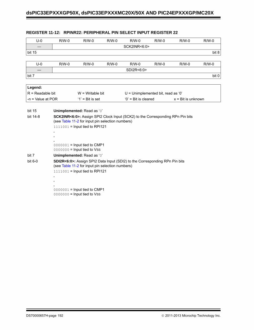
dsPIC33EPXXXGP50X, dsPIC33EPXXXMC20X/50X AND PIC24EPXXXGP/MC20X
REGISTER 11-12: RPINR22: PERIPHERAL PIN SELECT INPUT REGISTER 22
U-0 R/W-0 R/W-0 R/W-0 R/W-0 R/W-0 R/W-0 R/W-0
— SCK2INR<6:0>
bit 15 bit 8
U-0 R/W-0 R/W-0 R/W-0 R/W-0 R/W-0 R/W-0 R/W-0
— SDI2R<6:0>
bit 7 bit 0
Legend:
R = Readable bit W = Writable bit U = Unimplemented bit, read as ‘0’
-n = Value at POR ‘1’ = Bit is set ‘0’ = Bit is cleared x = Bit is unknown
bit 15 Unimplemented: Read as ‘0’
bit 14-8 SCK2INR<6:0>: Assign SPI2 Clock Input (SCK2) to the Corresponding RPn Pin bits(see Table 11-2 for input pin selection numbers)
1111001 = Input tied to RPI121...0000001 = Input tied to CMP10000000 = Input tied to VSS
bit 7 Unimplemented: Read as ‘0’
bit 6-0 SDI2R<6:0>: Assign SPI2 Data Input (SDI2) to the Corresponding RPn Pin bits(see Table 11-2 for input pin selection numbers)
1111001 = Input tied to RPI121...0000001 = Input tied to CMP10000000 = Input tied to VSS
DS70000657H-page 192 2011-2013 Microchip Technology Inc.

dsPIC33EPXXXGP50X, dsPIC33EPXXXMC20X/50X AND PIC24EPXXXGP/MC20X
REGISTER 11-13: RPINR23: PERIPHERAL PIN SELECT INPUT REGISTER 23
U-0 U-0 U-0 U-0 U-0 U-0 U-0 U-0
— — — — — — — —
bit 15 bit 8
U-0 R/W-0 R/W-0 R/W-0 R/W-0 R/W-0 R/W-0 R/W-0
— SS2R<6:0>
bit 7 bit 0
Legend:
R = Readable bit W = Writable bit U = Unimplemented bit, read as ‘0’
-n = Value at POR ‘1’ = Bit is set ‘0’ = Bit is cleared x = Bit is unknown
bit 15-7 Unimplemented: Read as ‘0’
bit 6-0 SS2R<6:0>: Assign SPI2 Slave Select (SS2) to the Corresponding RPn Pin bits(see Table 11-2 for input pin selection numbers)
1111001 = Input tied to RPI121...0000001 = Input tied to CMP10000000 = Input tied to VSS
REGISTER 11-14: RPINR26: PERIPHERAL PIN SELECT INPUT REGISTER 26 (dsPIC33EPXXXGP/MC50X DEVICES ONLY)
U-0 U-0 U-0 U-0 U-0 U-0 U-0 U-0
— — — — — — — —
bit 15 bit 8
U-0 R/W-0 R/W-0 R/W-0 R/W-0 R/W-0 R/W-0 R/W-0
— C1RXR<6:0>
bit 7 bit 0
Legend:
R = Readable bit W = Writable bit U = Unimplemented bit, read as ‘0’
-n = Value at POR ‘1’ = Bit is set ‘0’ = Bit is cleared x = Bit is unknown
bit 15-7 Unimplemented: Read as ‘0’
bit 6-0 C1RXR<6:0>: Assign CAN1 RX Input (CRX1) to the Corresponding RPn Pin bits(see Table 11-2 for input pin selection numbers)
1111001 = Input tied to RPI121...0000001 = Input tied to CMP10000000 = Input tied to VSS
2011-2013 Microchip Technology Inc. DS70000657H-page 193

dsPIC33EPXXXGP50X, dsPIC33EPXXXMC20X/50X AND PIC24EPXXXGP/MC20X
REGISTER 11-15: RPINR37: PERIPHERAL PIN SELECT INPUT REGISTER 37(dsPIC33EPXXXMC20X/50X AND PIC24EPXXXMC20X DEVICES ONLY)
U-0 R/W-0 R/W-0 R/W-0 R/W-0 R/W-0 R/W-0 R/W-0
— SYNCI1R<6:0>
bit 15 bit 8
U-0 U-0 U-0 U-0 U-0 U-0 U-0 U-0
— — — — — — — —
bit 7 bit 0
Legend:
R = Readable bit W = Writable bit U = Unimplemented bit, read as ‘0’
-n = Value at POR ‘1’ = Bit is set ‘0’ = Bit is cleared x = Bit is unknown
bit 15 Unimplemented: Read as ‘0’
bit 14-8 SYNCI1R<6:0>: Assign PWM Synchronization Input 1 to the Corresponding RPn Pin bits(see Table 11-2 for input pin selection numbers)
1111001 = Input tied to RPI121...0000001 = Input tied to CMP10000000 = Input tied to VSS
bit 7-0 Unimplemented: Read as ‘0’
DS70000657H-page 194 2011-2013 Microchip Technology Inc.

dsPIC33EPXXXGP50X, dsPIC33EPXXXMC20X/50X AND PIC24EPXXXGP/MC20X
REGISTER 11-16: RPINR38: PERIPHERAL PIN SELECT INPUT REGISTER 38 (dsPIC33EPXXXMC20X AND PIC24EPXXXMC20X DEVICES ONLY)
U-0 R/W-0 R/W-0 R/W-0 R/W-0 R/W-0 R/W-0 R/W-0
— DTCMP1R<6:0>
bit 15 bit 8
U-0 U-0 U-0 U-0 U-0 U-0 U-0 U-0
— — — — — — — —
bit 7 bit 0
Legend:
R = Readable bit W = Writable bit U = Unimplemented bit, read as ‘0’
-n = Value at POR ‘1’ = Bit is set ‘0’ = Bit is cleared x = Bit is unknown
bit 15 Unimplemented: Read as ‘0’
bit 14-8 DTCMP1R<6:0>: Assign PWM Dead-Time Compensation Input 1 to the Corresponding RPn Pin bits(see Table 11-2 for input pin selection numbers)
1111001 = Input tied to RPI121...0000001 = Input tied to CMP10000000 = Input tied to VSS
bit 7-0 Unimplemented: Read as ‘0’
2011-2013 Microchip Technology Inc. DS70000657H-page 195

dsPIC33EPXXXGP50X, dsPIC33EPXXXMC20X/50X AND PIC24EPXXXGP/MC20X
REGISTER 11-17: RPINR39: PERIPHERAL PIN SELECT INPUT REGISTER 39 (dsPIC33EPXXXMC20X/50X AND PIC24EPXXXMC20X DEVICES ONLY)
U-0 R/W-0 R/W-0 R/W-0 R/W-0 R/W-0 R/W-0 R/W-0
— DTCMP3R<6:0>
bit 15 bit 8
U-0 R/W-0 R/W-0 R/W-0 R/W-0 R/W-0 R/W-0 R/W-0
— DTCMP2R<6:0>
bit 7 bit 0
Legend:
R = Readable bit W = Writable bit U = Unimplemented bit, read as ‘0’
-n = Value at POR ‘1’ = Bit is set ‘0’ = Bit is cleared x = Bit is unknown
bit 15 Unimplemented: Read as ‘0’
bit 14-8 DTCMP3R<6:0>: Assign PWM Dead-Time Compensation Input 3 to the Corresponding RPn Pin bits(see Table 11-2 for input pin selection numbers)
1111001 = Input tied to RPI121...0000001 = Input tied to CMP10000000 = Input tied to VSS
bit 7 Unimplemented: Read as ‘0’
bit 6-0 DTCMP2R<6:0>: Assign PWM Dead-Time Compensation Input 2 to the Corresponding RPn Pin bits(see Table 11-2 for input pin selection numbers)
1111001 = Input tied to RPI121...0000001 = Input tied to CMP10000000 = Input tied to VSS
DS70000657H-page 196 2011-2013 Microchip Technology Inc.

dsPIC33EPXXXGP50X, dsPIC33EPXXXMC20X/50X AND PIC24EPXXXGP/MC20X
REGISTER 11-18: RPOR0: PERIPHERAL PIN SELECT OUTPUT REGISTER 0
U-0 U-0 R/W-0 R/W-0 R/W-0 R/W-0 R/W-0 R/W-0
— — RP35R<5:0>
bit 15 bit 8
U-0 U-0 R/W-0 R/W-0 R/W-0 R/W-0 R/W-0 R/W-0
— — RP20R<5:0>
bit 7 bit 0
Legend:
R = Readable bit W = Writable bit U = Unimplemented bit, read as ‘0’
-n = Value at POR ‘1’ = Bit is set ‘0’ = Bit is cleared x = Bit is unknown
bit 15-14 Unimplemented: Read as ‘0’
bit 13-8 RP35R<5:0>: Peripheral Output Function is Assigned to RP35 Output Pin bits (see Table 11-3 for peripheral function numbers)
bit 7-6 Unimplemented: Read as ‘0’
bit 5-0 RP20R<5:0>: Peripheral Output Function is Assigned to RP20 Output Pin bits (see Table 11-3 for peripheral function numbers)
REGISTER 11-19: RPOR1: PERIPHERAL PIN SELECT OUTPUT REGISTER 1
U-0 U-0 R/W-0 R/W-0 R/W-0 R/W-0 R/W-0 R/W-0
— — RP37R<5:0>
bit 15 bit 8
U-0 U-0 R/W-0 R/W-0 R/W-0 R/W-0 R/W-0 R/W-0
— — RP36R<5:0>
bit 7 bit 0
Legend:
R = Readable bit W = Writable bit U = Unimplemented bit, read as ‘0’
-n = Value at POR ‘1’ = Bit is set ‘0’ = Bit is cleared x = Bit is unknown
bit 15-14 Unimplemented: Read as ‘0’
bit 13-8 RP37R<5:0>: Peripheral Output Function is Assigned to RP37 Output Pin bits (see Table 11-3 for peripheral function numbers)
bit 7-6 Unimplemented: Read as ‘0’
bit 5-0 RP36R<5:0>: Peripheral Output Function is Assigned to RP36 Output Pin bits (see Table 11-3 for peripheral function numbers)
2011-2013 Microchip Technology Inc. DS70000657H-page 197

dsPIC33EPXXXGP50X, dsPIC33EPXXXMC20X/50X AND PIC24EPXXXGP/MC20X
REGISTER 11-20: RPOR2: PERIPHERAL PIN SELECT OUTPUT REGISTER 2
U-0 U-0 R/W-0 R/W-0 R/W-0 R/W-0 R/W-0 R/W-0
— — RP39R<5:0>
bit 15 bit 8
U-0 U-0 R/W-0 R/W-0 R/W-0 R/W-0 R/W-0 R/W-0
— — RP38R<5:0>
bit 7 bit 0
Legend:
R = Readable bit W = Writable bit U = Unimplemented bit, read as ‘0’
-n = Value at POR ‘1’ = Bit is set ‘0’ = Bit is cleared x = Bit is unknown
bit 15-14 Unimplemented: Read as ‘0’
bit 13-8 RP39R<5:0>: Peripheral Output Function is Assigned to RP39 Output Pin bits (see Table 11-3 for peripheral function numbers)
bit 7-6 Unimplemented: Read as ‘0’
bit 5-0 RP38R<5:0>: Peripheral Output Function is Assigned to RP38 Output Pin bits (see Table 11-3 for peripheral function numbers)
REGISTER 11-21: RPOR3: PERIPHERAL PIN SELECT OUTPUT REGISTER 3
U-0 U-0 R/W-0 R/W-0 R/W-0 R/W-0 R/W-0 R/W-0
— — RP41R<5:0>
bit 15 bit 8
U-0 U-0 R/W-0 R/W-0 R/W-0 R/W-0 R/W-0 R/W-0
— — RP40R<5:0>
bit 7 bit 0
Legend:
R = Readable bit W = Writable bit U = Unimplemented bit, read as ‘0’
-n = Value at POR ‘1’ = Bit is set ‘0’ = Bit is cleared x = Bit is unknown
bit 15-14 Unimplemented: Read as ‘0’
bit 13-8 RP41R<5:0>: Peripheral Output Function is Assigned to RP41 Output Pin bits (see Table 11-3 for peripheral function numbers)
bit 7-6 Unimplemented: Read as ‘0’
bit 5-0 RP40R<5:0>: Peripheral Output Function is Assigned to RP40 Output Pin bits (see Table 11-3 for peripheral function numbers)
DS70000657H-page 198 2011-2013 Microchip Technology Inc.

dsPIC33EPXXXGP50X, dsPIC33EPXXXMC20X/50X AND PIC24EPXXXGP/MC20X
REGISTER 11-22: RPOR4: PERIPHERAL PIN SELECT OUTPUT REGISTER 4
U-0 U-0 R/W-0 R/W-0 R/W-0 R/W-0 R/W-0 R/W-0
— — RP43R<5:0>
bit 15 bit 8
U-0 U-0 R/W-0 R/W-0 R/W-0 R/W-0 R/W-0 R/W-0
— — RP42R<5:0>
bit 7 bit 0
Legend:
R = Readable bit W = Writable bit U = Unimplemented bit, read as ‘0’
-n = Value at POR ‘1’ = Bit is set ‘0’ = Bit is cleared x = Bit is unknown
bit 15-14 Unimplemented: Read as ‘0’
bit 13-8 RP43R<5:0>: Peripheral Output Function is Assigned to RP43 Output Pin bits (see Table 11-3 for peripheral function numbers)
bit 7-6 Unimplemented: Read as ‘0’
bit 5-0 RP42R<5:0>: Peripheral Output Function is Assigned to RP42 Output Pin bits (see Table 11-3 for peripheral function numbers)
REGISTER 11-23: RPOR5: PERIPHERAL PIN SELECT OUTPUT REGISTER 5
U-0 U-0 R/W-0 R/W-0 R/W-0 R/W-0 R/W-0 R/W-0
— — RP55R<5:0>
bit 15 bit 8
U-0 U-0 R/W-0 R/W-0 R/W-0 R/W-0 R/W-0 R/W-0
— — RP54R<5:0>
bit 7 bit 0
Legend:
R = Readable bit W = Writable bit U = Unimplemented bit, read as ‘0’
-n = Value at POR ‘1’ = Bit is set ‘0’ = Bit is cleared x = Bit is unknown
bit 15-14 Unimplemented: Read as ‘0’
bit 13-8 RP55R<5:0>: Peripheral Output Function is Assigned to RP55 Output Pin bits (see Table 11-3 for peripheral function numbers)
bit 7-6 Unimplemented: Read as ‘0’
bit 5-0 RP54R<5:0>: Peripheral Output Function is Assigned to RP54 Output Pin bits (see Table 11-3 for peripheral function numbers)
2011-2013 Microchip Technology Inc. DS70000657H-page 199

dsPIC33EPXXXGP50X, dsPIC33EPXXXMC20X/50X AND PIC24EPXXXGP/MC20X
REGISTER 11-24: RPOR6: PERIPHERAL PIN SELECT OUTPUT REGISTER 6
U-0 U-0 R/W-0 R/W-0 R/W-0 R/W-0 R/W-0 R/W-0
— — RP57R<5:0>
bit 15 bit 8
U-0 U-0 R/W-0 R/W-0 R/W-0 R/W-0 R/W-0 R/W-0
— — RP56R<5:0>
bit 7 bit 0
Legend:
R = Readable bit W = Writable bit U = Unimplemented bit, read as ‘0’
-n = Value at POR ‘1’ = Bit is set ‘0’ = Bit is cleared x = Bit is unknown
bit 15-14 Unimplemented: Read as ‘0’
bit 13-8 RP57R<5:0>: Peripheral Output Function is Assigned to RP57 Output Pin bits (see Table 11-3 for peripheral function numbers)
bit 7-6 Unimplemented: Read as ‘0’
bit 5-0 RP56R<5:0>: Peripheral Output Function is Assigned to RP56 Output Pin bits (see Table 11-3 for peripheral function numbers)
REGISTER 11-25: RPOR7: PERIPHERAL PIN SELECT OUTPUT REGISTER 7
U-0 U-0 R/W-0 R/W-0 R/W-0 R/W-0 R/W-0 R/W-0
— — RP97R<5:0>
bit 15 bit 8
U-0 U-0 U-0 U-0 U-0 U-0 U-0 U-0
— — — — — — — —
bit 7 bit 0
Legend:
R = Readable bit W = Writable bit U = Unimplemented bit, read as ‘0’
-n = Value at POR ‘1’ = Bit is set ‘0’ = Bit is cleared x = Bit is unknown
bit 15-14 Unimplemented: Read as ‘0’
bit 13-8 RP97R<5:0>: Peripheral Output Function is Assigned to RP97 Output Pin bits (see Table 11-3 for peripheral function numbers)
bit 7-0 Unimplemented: Read as ‘0’
DS70000657H-page 200 2011-2013 Microchip Technology Inc.

dsPIC33EPXXXGP50X, dsPIC33EPXXXMC20X/50X AND PIC24EPXXXGP/MC20X
REGISTER 11-26: RPOR8: PERIPHERAL PIN SELECT OUTPUT REGISTER 8
U-0 U-0 R/W-0 R/W-0 R/W-0 R/W-0 R/W-0 R/W-0
— — RP118R<5:0>
bit 15 bit 8
U-0 U-0 U-0 U-0 U-0 U-0 U-0 U-0
— — — — — — — —
bit 7 bit 0
Legend:
R = Readable bit W = Writable bit U = Unimplemented bit, read as ‘0’
-n = Value at POR ‘1’ = Bit is set ‘0’ = Bit is cleared x = Bit is unknown
bit 15-14 Unimplemented: Read as ‘0’
bit 13-8 RP118R<5:0>: Peripheral Output Function is Assigned to RP118 Output Pin bits (see Table 11-3 for peripheral function numbers)
bit 7-0 Unimplemented: Read as ‘0’
REGISTER 11-27: RPOR9: PERIPHERAL PIN SELECT OUTPUT REGISTER 9
U-0 U-0 U-0 U-0 U-0 U-0 U-0 U-0
— — — — — — — —
bit 15 bit 8
U-0 U-0 R/W-0 R/W-0 R/W-0 R/W-0 R/W-0 R/W-0
— — RP120R<5:0>
bit 7 bit 0
Legend:
R = Readable bit W = Writable bit U = Unimplemented bit, read as ‘0’
-n = Value at POR ‘1’ = Bit is set ‘0’ = Bit is cleared x = Bit is unknown
bit 15-6 Unimplemented: Read as ‘0’
bit 5-0 RP120R<5:0>: Peripheral Output Function is Assigned to RP120 Output Pin bits (see Table 11-3 for peripheral function numbers)
2011-2013 Microchip Technology Inc. DS70000657H-page 201

dsPIC33EPXXXGP50X, dsPIC33EPXXXMC20X/50X AND PIC24EPXXXGP/MC20X
NOTES:
DS70000657H-page 202 2011-2013 Microchip Technology Inc.

dsPIC33EPXXXGP50X, dsPIC33EPXXXMC20X/50X AND PIC24EPXXXGP/MC20X
12.0 TIMER1
The Timer1 module is a 16-bit timer that can operate asa free-running interval timer/counter.
The Timer1 module has the following unique featuresover other timers:
• Can be operated in Asynchronous Counter mode from an external clock source
• The external clock input (T1CK) can optionally be synchronized to the internal device clock and the clock synchronization is performed after the prescaler
A block diagram of Timer1 is shown in Figure 12-1.
The Timer1 module can operate in one of the followingmodes:
• Timer mode
• Gated Timer mode
• Synchronous Counter mode
• Asynchronous Counter mode
In Timer and Gated Timer modes, the input clock isderived from the internal instruction cycle clock (FCY).In Synchronous and Asynchronous Counter modes,the input clock is derived from the external clock inputat the T1CK pin.
The Timer modes are determined by the following bits:
• Timer Clock Source Control bit (TCS): T1CON<1>
• Timer Synchronization Control bit (TSYNC): T1CON<2>
• Timer Gate Control bit (TGATE): T1CON<6>
Timer control bit setting for different operating modesare given in the Table 12-1.
TABLE 12-1: TIMER MODE SETTINGS
FIGURE 12-1: 16-BIT TIMER1 MODULE BLOCK DIAGRAM
Note 1: This data sheet summarizes thefeatures of the dsPIC33EPXXXGP50X,dsPIC33EPXXXMC20X/50X andPIC24EPXXXGP/MC20X families ofdevices. It is not intended to be acomprehensive reference source. To com-plement the information in this data sheet,refer to “Timers” (DS70362) in the“dsPIC33/PIC24 Family Reference Man-ual”, which is available from the Microchipweb site (www.microchip.com).
2: Some registers and associated bitsdescribed in this section may not beavailable on all devices. Refer toSection 4.0 “Memory Organization” inthis data sheet for device-specific registerand bit information.
Mode TCS TGATE TSYNC
Timer 0 0 x
Gated Timer 0 1 x
Synchronous Counter
1 x 1
Asynchronous Counter
1 x 0
TGATE
TCS
00
10
x1
PR1
TGATE
Set T1IF Flag
0
1
TSYNC
1
0
SyncEqual
Reset
T1CKPrescaler
(/n)
TCKPS<1:0>
GateSync
FP(1)
Falling EdgeDetect
TCKPS<1:0>
Note 1: FP is the peripheral clock.
LatchData
CLK
T1CLK
CTMUEdge Control
Logic
TMR1
Comparator
Prescaler(/n)
2011-2013 Microchip Technology Inc. DS70000657H-page 203

dsPIC33EPXXXGP50X, dsPIC33EPXXXMC20X/50X AND PIC24EPXXXGP/MC20X
12.1 Timer1 Resources
Many useful resources are provided on the main prod-uct page of the Microchip web site for the devices listedin this data sheet. This product page, which can beaccessed using this link, contains the latest updatesand additional information.
12.1.1 KEY RESOURCES
• “Timers” (DS70362) in the “dsPIC33/PIC24 Family Reference Manual”
• Code Samples
• Application Notes
• Software Libraries
• Webinars
• All Related “dsPIC33/PIC24 Family Reference Manual” Sections
• Development Tools
Note: In the event you are not able to access theproduct page using the link above, enterthis URL in your browser:http://www.microchip.com/wwwproducts/Devices.aspx?dDocName=en555464
DS70000657H-page 204 2011-2013 Microchip Technology Inc.
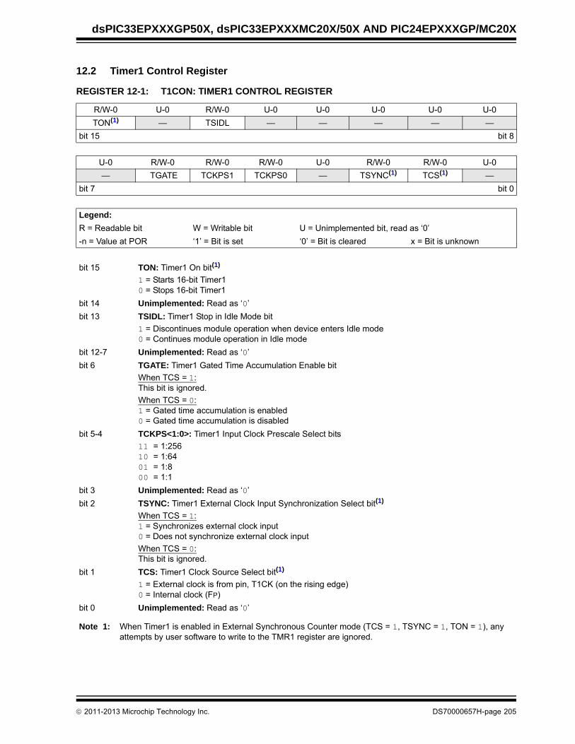
dsPIC33EPXXXGP50X, dsPIC33EPXXXMC20X/50X AND PIC24EPXXXGP/MC20X
12.2 Timer1 Control Register
REGISTER 12-1: T1CON: TIMER1 CONTROL REGISTER
R/W-0 U-0 R/W-0 U-0 U-0 U-0 U-0 U-0
TON(1) — TSIDL — — — — —
bit 15 bit 8
U-0 R/W-0 R/W-0 R/W-0 U-0 R/W-0 R/W-0 U-0
— TGATE TCKPS1 TCKPS0 — TSYNC(1) TCS(1) —
bit 7 bit 0
Legend:
R = Readable bit W = Writable bit U = Unimplemented bit, read as ‘0’
-n = Value at POR ‘1’ = Bit is set ‘0’ = Bit is cleared x = Bit is unknown
bit 15 TON: Timer1 On bit(1)
1 = Starts 16-bit Timer10 = Stops 16-bit Timer1
bit 14 Unimplemented: Read as ‘0’
bit 13 TSIDL: Timer1 Stop in Idle Mode bit
1 = Discontinues module operation when device enters Idle mode0 = Continues module operation in Idle mode
bit 12-7 Unimplemented: Read as ‘0’
bit 6 TGATE: Timer1 Gated Time Accumulation Enable bit
When TCS = 1: This bit is ignored.
When TCS = 0: 1 = Gated time accumulation is enabled0 = Gated time accumulation is disabled
bit 5-4 TCKPS<1:0>: Timer1 Input Clock Prescale Select bits
11 = 1:256 10 = 1:6401 = 1:8 00 = 1:1
bit 3 Unimplemented: Read as ‘0’
bit 2 TSYNC: Timer1 External Clock Input Synchronization Select bit(1)
When TCS = 1: 1 = Synchronizes external clock input0 = Does not synchronize external clock input
When TCS = 0: This bit is ignored.
bit 1 TCS: Timer1 Clock Source Select bit(1)
1 = External clock is from pin, T1CK (on the rising edge) 0 = Internal clock (FP)
bit 0 Unimplemented: Read as ‘0’
Note 1: When Timer1 is enabled in External Synchronous Counter mode (TCS = 1, TSYNC = 1, TON = 1), any attempts by user software to write to the TMR1 register are ignored.
2011-2013 Microchip Technology Inc. DS70000657H-page 205

dsPIC33EPXXXGP50X, dsPIC33EPXXXMC20X/50X AND PIC24EPXXXGP/MC20X
NOTES:
DS70000657H-page 206 2011-2013 Microchip Technology Inc.

dsPIC33EPXXXGP50X, dsPIC33EPXXXMC20X/50X AND PIC24EPXXXGP/MC20X
13.0 TIMER2/3 AND TIMER4/5
The Timer2/3 and Timer4/5 modules are 32-bit timers,which can also be configured as four independent16-bit timers with selectable operating modes.
As 32-bit timers, Timer2/3 and Timer4/5 operate inthree modes:
• Two Independent 16-Bit Timers (e.g., Timer2 and Timer3) with all 16-Bit Operating modes (except Asynchronous Counter mode)
• Single 32-Bit Timer
• Single 32-Bit Synchronous Counter
They also support these features:
• Timer Gate Operation
• Selectable Prescaler Settings
• Timer Operation during Idle and Sleep modes
• Interrupt on a 32-Bit Period Register Match
• Time Base for Input Capture and Output Compare Modules (Timer2 and Timer3 only)
• ADC1 Event Trigger (32-bit timer pairs, and Timer3 and Timer5 only)
Individually, all four of the 16-bit timers can function assynchronous timers or counters. They also offer thefeatures listed previously, except for the event trigger;this is implemented only with Timer2/3. The operatingmodes and enabled features are determined by settingthe appropriate bit(s) in the T2CON, T3CON, andT4CON, T5CON registers. T2CON and T4CON areshown in generic form in Register 13-1. T3CON andT5CON are shown in Register 13-2.
For 32-bit timer/counter operation, Timer2 and Timer4are the least significant word (lsw); Timer3 and Timer5are the most significant word (msw) of the 32-bit timers.
A block diagram for an example 32-bit timer pair (Tim-er2/3 and Timer4/5) is shown in Figure 13-3.
Note 1: This data sheet summarizes thefeatures of the dsPIC33EPXXXGP50X,dsPIC33EPXXXMC20X/50X andPIC24EPXXXGP/MC20X family ofdevices. It is not intended to be acomprehensive reference source. To com-plement the information in this data sheet,refer to “Timers” (DS70362) of the“dsPIC33/PIC24 Family ReferenceManual”, which is available from theMicrochip web site (www.microchip.com).
2: Some registers and associated bitsdescribed in this section may not beavailable on all devices. Refer toSection 4.0 “Memory Organization” inthis data sheet for device-specific registerand bit information.
Note: For 32-bit operation, T3CON and T5CONcontrol bits are ignored. Only T2CON andT4CON control bits are used for setup andcontrol. Timer2 and Timer4 clock and gateinputs are utilized for the 32-bit timermodules, but an interrupt is generatedwith the Timer3 and Timer5 interrupt flags.
Note: Only Timer2, 3, 4 and 5 can trigger a DMAdata transfer.
2011-2013 Microchip Technology Inc. DS70000657H-page 207

dsPIC33EPXXXGP50X, dsPIC33EPXXXMC20X/50X AND PIC24EPXXXGP/MC20X
FIGURE 13-1: TYPE B TIMER BLOCK DIAGRAM (x = 2 AND 4)
FIGURE 13-2: TYPE C TIMER BLOCK DIAGRAM (x = 3 AND 5)
Note 1: FP is the peripheral clock.
TGATE
TCS
00
10
x1
PRx
TGATE
Set TxIF Flag
0
1
Equal
Reset
TxCK
TCKPS<1:0>
GateSync
FP(1)
Falling EdgeDetect
TCKPS<1:0>Latch
Data
CLK
TxCLK
TMRx
Comparator
Prescaler(/n)
Prescaler(/n)
Sync
Note 1: FP is the peripheral clock.2: The ADC trigger is available on TMR3 and TMR5 only.
TGATE
TCS
00
10
x1
PRx
TGATE
Set TxIF Flag
0
1
Equal
Reset
TxCK
TCKPS<1:0>
GateSync
FP(1)
Falling EdgeDetect
TCKPS<1:0>Latch
Data
CLK
TxCLK
TMRx
Comparator
Prescaler(/n)
Prescaler(/n)
Sync
ADC Start ofConversion Trigger(2)
DS70000657H-page 208 2011-2013 Microchip Technology Inc.

dsPIC33EPXXXGP50X, dsPIC33EPXXXMC20X/50X AND PIC24EPXXXGP/MC20X
FIGURE 13-3: TYPE B/TYPE C TIMER PAIR BLOCK DIAGRAM (32-BIT TIMER)
13.1 Timerx/y Resources
Many useful resources are provided on the main prod-uct page of the Microchip web site for the devices listedin this data sheet. This product page, which can beaccessed using this link, contains the latest updatesand additional information.
13.1.1 KEY RESOURCES
• “Timers” (DS70362) in the “dsPIC33/PIC24 Family Reference Manual”
• Code Samples
• Application Notes
• Software Libraries
• Webinars
• All Related “dsPIC33/PIC24 Family Reference Manual” Sections
• Development Tools
TGATE
TCS
00
10
x1
Comparator
TGATE
Set TyIF Flag
0
1
Equal
Reset
TxCK
TCKPS<1:0>
FP(1)
TCKPS<1:0>
Note 1: The ADC trigger is available on the TMR3:TMR2 andTMR5:TMR4 32-bit timer pairs.2: Timerx is a Type B timer (x = 2 and 4).3: Timery is a Type C timer (y = 3 and 5).
Latch
Data
CLK
ADC
PRx
TMRyHLD
Data Bus<15:0>
mswlsw
Prescaler(/n)
Prescaler(/n)
Sync
GateSync
Falling EdgeDetect
PRy
TMRx TMRy
Note: In the event you are not able to access theproduct page using the link above, enterthis URL in your browser:http://www.microchip.com/wwwproducts/Devices.aspx?dDocName=en555464
2011-2013 Microchip Technology Inc. DS70000657H-page 209

dsPIC33EPXXXGP50X, dsPIC33EPXXXMC20X/50X AND PIC24EPXXXGP/MC20X
13.2 Timer Control Registers
REGISTER 13-1: TxCON: (TIMER2 AND TIMER4) CONTROL REGISTER
R/W-0 U-0 R/W-0 U-0 U-0 U-0 U-0 U-0
TON — TSIDL — — — — —
bit 15 bit 8
U-0 R/W-0 R/W-0 R/W-0 R/W-0 U-0 R/W-0 U-0
— TGATE TCKPS1 TCKPS0 T32 — TCS —
bit 7 bit 0
Legend:
R = Readable bit W = Writable bit U = Unimplemented bit, read as ‘0’
-n = Value at POR ‘1’ = Bit is set ‘0’ = Bit is cleared x = Bit is unknown
bit 15 TON: Timerx On bit
When T32 = 1:1 = Starts 32-bit Timerx/y0 = Stops 32-bit Timerx/y
When T32 = 0:1 = Starts 16-bit Timerx0 = Stops 16-bit Timerx
bit 14 Unimplemented: Read as ‘0’
bit 13 TSIDL: Timerx Stop in Idle Mode bit
1 = Discontinues module operation when device enters Idle mode0 = Continues module operation in Idle mode
bit 12-7 Unimplemented: Read as ‘0’
bit 6 TGATE: Timerx Gated Time Accumulation Enable bit
When TCS = 1:This bit is ignored.
When TCS = 0:1 = Gated time accumulation is enabled0 = Gated time accumulation is disabled
bit 5-4 TCKPS<1:0>: Timerx Input Clock Prescale Select bits
11 = 1:256 10 = 1:6401 = 1:8 00 = 1:1
bit 3 T32: 32-Bit Timer Mode Select bit
1 = Timerx and Timery form a single 32-bit timer0 = Timerx and Timery act as two 16-bit timers
bit 2 Unimplemented: Read as ‘0’
bit 1 TCS: Timerx Clock Source Select bit
1 = External clock is from pin, TxCK (on the rising edge) 0 = Internal clock (FP)
bit 0 Unimplemented: Read as ‘0’
DS70000657H-page 210 2011-2013 Microchip Technology Inc.

dsPIC33EPXXXGP50X, dsPIC33EPXXXMC20X/50X AND PIC24EPXXXGP/MC20X
REGISTER 13-2: TyCON: (TIMER3 AND TIMER5) CONTROL REGISTER
R/W-0 U-0 R/W-0 U-0 U-0 U-0 U-0 U-0
TON(1) — TSIDL(2) — — — — —
bit 15 bit 8
U-0 R/W-0 R/W-0 R/W-0 U-0 U-0 R/W-0 U-0
— TGATE(1) TCKPS1(1) TCKPS0(1) — — TCS(1,3) —
bit 7 bit 0
Legend:
R = Readable bit W = Writable bit U = Unimplemented bit, read as ‘0’
-n = Value at POR ‘1’ = Bit is set ‘0’ = Bit is cleared x = Bit is unknown
bit 15 TON: Timery On bit(1)
1 = Starts 16-bit Timery0 = Stops 16-bit Timery
bit 14 Unimplemented: Read as ‘0’
bit 13 TSIDL: Timery Stop in Idle Mode bit(2)
1 = Discontinues module operation when device enters Idle mode0 = Continues module operation in Idle mode
bit 12-7 Unimplemented: Read as ‘0’
bit 6 TGATE: Timery Gated Time Accumulation Enable bit(1)
When TCS = 1: This bit is ignored.
When TCS = 0: 1 = Gated time accumulation is enabled0 = Gated time accumulation is disabled
bit 5-4 TCKPS<1:0>: Timery Input Clock Prescale Select bits(1)
11 = 1:256 10 = 1:6401 = 1:8 00 = 1:1
bit 3-2 Unimplemented: Read as ‘0’
bit 1 TCS: Timery Clock Source Select bit(1,3)
1 = External clock is from pin, TyCK (on the rising edge) 0 = Internal clock (FP)
bit 0 Unimplemented: Read as ‘0’
Note 1: When 32-bit operation is enabled (T2CON<3> = 1), these bits have no effect on Timery operation; all timer functions are set through TxCON.
2: When 32-bit timer operation is enabled (T32 = 1) in the Timerx Control register (TxCON<3>), the TSIDL bit must be cleared to operate the 32-bit timer in Idle mode.
3: The TyCK pin is not available on all timers. See the “Pin Diagrams” section for the available pins.
2011-2013 Microchip Technology Inc. DS70000657H-page 211

dsPIC33EPXXXGP50X, dsPIC33EPXXXMC20X/50X AND PIC24EPXXXGP/MC20X
NOTES:
DS70000657H-page 212 2011-2013 Microchip Technology Inc.

dsPIC33EPXXXGP50X, dsPIC33EPXXXMC20X/50X AND PIC24EPXXXGP/MC20X
14.0 INPUT CAPTURE The input capture module is useful in applicationsrequiring frequency (period) and pulse measurement.The dsPIC33EPXXXGP50X, dsPIC33EPXXXMC20X/50X and PIC24EPXXXGP/MC20X devices supportfour input capture channels.
Key features of the input capture module include:
• Hardware-configurable for 32-bit operation in all modes by cascading two adjacent modules
• Synchronous and Trigger modes of output compare operation, with up to 19 user-selectable Trigger/Sync sources available
• A 4-level FIFO buffer for capturing and holding timer values for several events
• Configurable interrupt generation
• Up to six clock sources available for each module, driving a separate internal 16-bit counter
FIGURE 14-1: INPUT CAPTURE x MODULE BLOCK DIAGRAM
Note 1: This data sheet summarizes thefeatures of the dsPIC33EPXXXGP50X,dsPIC33EPXXXMC20X/50X andPIC24EPXXXGP/MC20X families ofdevices. It is not intended to be acomprehensive reference source. Tocomplement the information in this datasheet, refer to “Input Capture”(DS70352) in the “dsPIC33/dsPIC24Family Reference Manual”, which isavailable from the Microchip web site(www.microchip.com).
2: Some registers and associated bitsdescribed in this section may not beavailable on all devices. Refer toSection 4.0 “Memory Organization” inthis data sheet for device-specific registerand bit information.
ICxBUF
4-Level FIFO Buffer
ICx Pin
ICM<2:0>
Set ICxIFEdge Detect Logic
ICI<1:0>
ICOV, ICBNE
InterruptLogic
System Bus
PrescalerCounter1:1/4/16
andClock Synchronizer
Event and
Trigger andSync Logic
ClockSelect
IC ClockSources
Trigger andSync Sources
ICTSEL<2:0>
SYNCSEL<4:0>Trigger(1)
16
16
16ICxTMR
Increment
Reset
Note 1: The Trigger/Sync source is enabled by default and is set to Timer3 as a source. This timer must be enabled for proper ICx module operation or the Trigger/Sync source must be changed to another source option.
PTG TriggerInput
CTMU EdgeControl Logic
2011-2013 Microchip Technology Inc. DS70000657H-page 213

dsPIC33EPXXXGP50X, dsPIC33EPXXXMC20X/50X AND PIC24EPXXXGP/MC20X
14.1 Input Capture Resources
Many useful resources are provided on the main prod-uct page of the Microchip web site for the devices listedin this data sheet. This product page, which can beaccessed using this link, contains the latest updatesand additional information.
14.1.1 KEY RESOURCES
• “Input Capture” (DS70352) in the “dsPIC33/PIC24 Family Reference Manual”
• Code Samples
• Application Notes
• Software Libraries
• Webinars
• All Related “dsPIC33/PIC24 Family Reference Manual” Sections
• Development Tools
Note: In the event you are not able to access theproduct page using the link above, enterthis URL in your browser:http://www.microchip.com/wwwproducts/Devices.aspx?dDocName=en555464
DS70000657H-page 214 2011-2013 Microchip Technology Inc.

dsPIC33EPXXXGP50X, dsPIC33EPXXXMC20X/50X AND PIC24EPXXXGP/MC20X
14.2 Input Capture Registers
REGISTER 14-1: ICxCON1: INPUT CAPTURE x CONTROL REGISTER 1
U-0 U-0 R/W-0 R/W-0 R/W-0 R/W-0 U-0 U-0
— — ICSIDL ICTSEL2 ICTSEL1 ICTSEL0 — —
bit 15 bit 8
U-0 R/W-0 R/W-0 R/HC/HS-0 R/HC/HS-0 R/W-0 R/W-0 R/W-0
— ICI1 ICI0 ICOV ICBNE ICM2 ICM1 ICM0
bit 7 bit 0
Legend: HC = Hardware Clearable bit HS = Hardware Settable bit
R = Readable bit W = Writable bit U = Unimplemented bit, read as ‘0’
-n = Value at POR ‘1’ = Bit is set ‘0’ = Bit is cleared x = Bit is unknown
bit 15-14 Unimplemented: Read as ‘0’
bit 13 ICSIDL: Input Capture Stop in Idle Control bit
1 = Input capture will Halt in CPU Idle mode0 = Input capture will continue to operate in CPU Idle mode
bit 12-10 ICTSEL<2:0>: Input Capture Timer Select bits
111 = Peripheral clock (FP) is the clock source of the ICx110 = Reserved101 = Reserved100 = T1CLK is the clock source of the ICx (only the synchronous clock is supported)011 = T5CLK is the clock source of the ICx010 = T4CLK is the clock source of the ICx001 = T2CLK is the clock source of the ICx000 = T3CLK is the clock source of the ICx
bit 9-7 Unimplemented: Read as ‘0’
bit 6-5 ICI<1:0>: Number of Captures per Interrupt Select bits (this field is not used if ICM<2:0> = 001 or 111)
11 = Interrupt on every fourth capture event10 = Interrupt on every third capture event01 = Interrupt on every second capture event00 = Interrupt on every capture event
bit 4 ICOV: Input Capture Overflow Status Flag bit (read-only)
1 = Input capture buffer overflow occurred0 = No input capture buffer overflow occurred
bit 3 ICBNE: Input Capture Buffer Not Empty Status bit (read-only)
1 = Input capture buffer is not empty, at least one more capture value can be read0 = Input capture buffer is empty
bit 2-0 ICM<2:0>: Input Capture Mode Select bits
111 = Input capture functions as interrupt pin only in CPU Sleep and Idle modes (rising edge detectonly, all other control bits are not applicable)
110 = Unused (module is disabled)101 = Capture mode, every 16th rising edge (Prescaler Capture mode)100 = Capture mode, every 4th rising edge (Prescaler Capture mode)011 = Capture mode, every rising edge (Simple Capture mode)010 = Capture mode, every falling edge (Simple Capture mode)001 = Capture mode, every edge rising and falling (Edge Detect mode (ICI<1:0>) is not used in this mode)000 = Input capture module is turned off
2011-2013 Microchip Technology Inc. DS70000657H-page 215

dsPIC33EPXXXGP50X, dsPIC33EPXXXMC20X/50X AND PIC24EPXXXGP/MC20X
REGISTER 14-2: ICxCON2: INPUT CAPTURE x CONTROL REGISTER 2
U-0 U-0 U-0 U-0 U-0 U-0 U-0 R/W-0
— — — — — — — IC32
bit 15 bit 8
R/W-0 R/W/HS-0 U-0 R/W-0 R/W-1 R/W-1 R/W-0 R/W-1
ICTRIG(2) TRIGSTAT(3) — SYNCSEL4(4) SYNCSEL3(4) SYNCSEL2(4) SYNCSEL1(4) SYNCSEL0(4)
bit 7 bit 0
Legend: HS = Hardware Settable bit
R = Readable bit W = Writable bit U = Unimplemented bit, read as ‘0’
-n = Value at POR ‘1’ = Bit is set ‘0’ = Bit is cleared x = Bit is unknown
bit 15-9 Unimplemented: Read as ‘0’
bit 8 IC32: Input Capture 32-Bit Timer Mode Select bit (Cascade mode)
1 = Odd IC and Even IC form a single 32-bit input capture module(1)
0 = Cascade module operation is disabled
bit 7 ICTRIG: Input Capture Trigger Operation Select bit(2)
1 = Input source used to trigger the input capture timer (Trigger mode)0 = Input source used to synchronize the input capture timer to a timer of another module
(Synchronization mode)
bit 6 TRIGSTAT: Timer Trigger Status bit(3)
1 = ICxTMR has been triggered and is running0 = ICxTMR has not been triggered and is being held clear
bit 5 Unimplemented: Read as ‘0’
Note 1: The IC32 bit in both the Odd and Even IC must be set to enable Cascade mode.
2: The input source is selected by the SYNCSEL<4:0> bits of the ICxCON2 register.
3: This bit is set by the selected input source (selected by SYNCSEL<4:0> bits). It can be read, set and cleared in software.
4: Do not use the ICx module as its own Sync or Trigger source.
5: This option should only be selected as a trigger source and not as a synchronization source.
6: Each Input Capture x (ICx) module has one PTG input source. See Section 24.0 “Peripheral Trigger Generator (PTG) Module” for more information.PTGO8 = IC1PTGO9 = IC2PTGO10 = IC3PTGO11 = IC4
DS70000657H-page 216 2011-2013 Microchip Technology Inc.
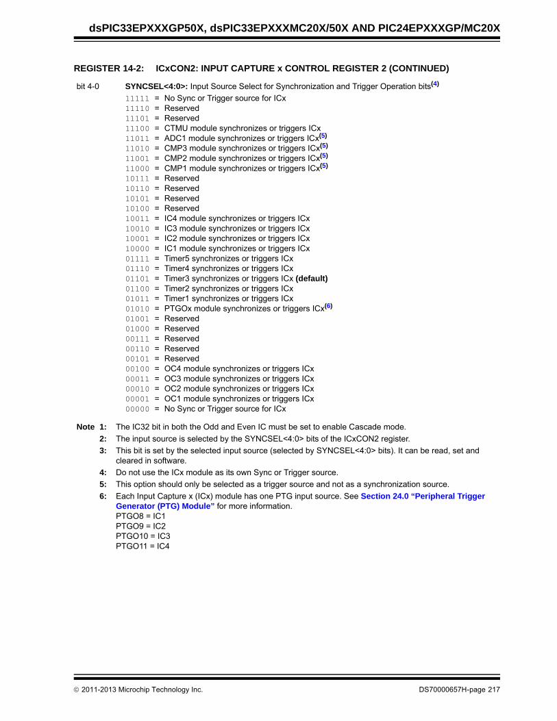
dsPIC33EPXXXGP50X, dsPIC33EPXXXMC20X/50X AND PIC24EPXXXGP/MC20X
bit 4-0 SYNCSEL<4:0>: Input Source Select for Synchronization and Trigger Operation bits(4)
11111 = No Sync or Trigger source for ICx11110 = Reserved11101 = Reserved11100 = CTMU module synchronizes or triggers ICx11011 = ADC1 module synchronizes or triggers ICx(5)
11010 = CMP3 module synchronizes or triggers ICx(5)
11001 = CMP2 module synchronizes or triggers ICx(5)
11000 = CMP1 module synchronizes or triggers ICx(5)
10111 = Reserved10110 = Reserved10101 = Reserved10100 = Reserved10011 = IC4 module synchronizes or triggers ICx10010 = IC3 module synchronizes or triggers ICx10001 = IC2 module synchronizes or triggers ICx10000 = IC1 module synchronizes or triggers ICx01111 = Timer5 synchronizes or triggers ICx01110 = Timer4 synchronizes or triggers ICx01101 = Timer3 synchronizes or triggers ICx (default)01100 = Timer2 synchronizes or triggers ICx01011 = Timer1 synchronizes or triggers ICx01010 = PTGOx module synchronizes or triggers ICx(6)
01001 = Reserved01000 = Reserved00111 = Reserved00110 = Reserved00101 = Reserved00100 = OC4 module synchronizes or triggers ICx00011 = OC3 module synchronizes or triggers ICx00010 = OC2 module synchronizes or triggers ICx00001 = OC1 module synchronizes or triggers ICx00000 = No Sync or Trigger source for ICx
REGISTER 14-2: ICxCON2: INPUT CAPTURE x CONTROL REGISTER 2 (CONTINUED)
Note 1: The IC32 bit in both the Odd and Even IC must be set to enable Cascade mode.
2: The input source is selected by the SYNCSEL<4:0> bits of the ICxCON2 register.
3: This bit is set by the selected input source (selected by SYNCSEL<4:0> bits). It can be read, set and cleared in software.
4: Do not use the ICx module as its own Sync or Trigger source.
5: This option should only be selected as a trigger source and not as a synchronization source.
6: Each Input Capture x (ICx) module has one PTG input source. See Section 24.0 “Peripheral Trigger Generator (PTG) Module” for more information.PTGO8 = IC1PTGO9 = IC2PTGO10 = IC3PTGO11 = IC4
2011-2013 Microchip Technology Inc. DS70000657H-page 217

dsPIC33EPXXXGP50X, dsPIC33EPXXXMC20X/50X AND PIC24EPXXXGP/MC20X
NOTES:
DS70000657H-page 218 2011-2013 Microchip Technology Inc.
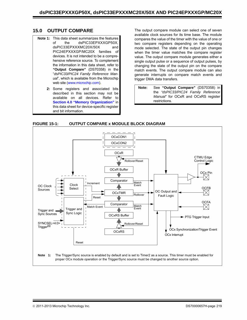
dsPIC33EPXXXGP50X, dsPIC33EPXXXMC20X/50X AND PIC24EPXXXGP/MC20X
15.0 OUTPUT COMPARE The output compare module can select one of sevenavailable clock sources for its time base. The modulecompares the value of the timer with the value of one ortwo compare registers depending on the operatingmode selected. The state of the output pin changeswhen the timer value matches the compare registervalue. The output compare module generates either asingle output pulse or a sequence of output pulses, bychanging the state of the output pin on the comparematch events. The output compare module can alsogenerate interrupts on compare match events andtrigger DMA data transfers.
FIGURE 15-1: OUTPUT COMPARE x MODULE BLOCK DIAGRAM
Note 1: This data sheet summarizes the featuresof the dsPIC33EPXXXGP50X,dsPIC33EPXXXMC20X/50X andPIC24EPXXXGP/MC20X families ofdevices. It is not intended to be a compre-hensive reference source. To complementthe information in this data sheet, refer to“Output Compare” (DS70358) in the“dsPIC33/PIC24 Family Reference Man-ual”, which is available from the Microchipweb site (www.microchip.com).
2: Some registers and associated bitsdescribed in this section may not beavailable on all devices. Refer toSection 4.0 “Memory Organization” inthis data sheet for device-specific registerand bit information.
Note: See “Output Compare” (DS70358) inthe “dsPIC33/PIC24 Family ReferenceManual” for OCxR and OCxRS registerrestrictions.
OCxR Buffer
Comparator
OCxTMR
OCxCON1
OCxCON2
OCx Interrupt
OCx Pin
OCxRS Buffer
Comparator
Match
Match Trigger andSync Logic
ClockSelect
Increment
Reset
OC ClockSources
Trigger andSync Sources
Reset
Match Event
OCFA
OCxR
OCxRS
Event
Event
Rollover
Rollover/Reset
Rollover/Reset
OCx Synchronization/Trigger Event
OCFB
SYNCSEL<4:0>Trigger(1)
Note 1: The Trigger/Sync source is enabled by default and is set to Timer2 as a source. This timer must be enabled for proper OCx module operation or the Trigger/Sync source must be changed to another source option.
PTG Trigger Input
CTMU EdgeControl Logic
OC Output andFault Logic
2011-2013 Microchip Technology Inc. DS70000657H-page 219

dsPIC33EPXXXGP50X, dsPIC33EPXXXMC20X/50X AND PIC24EPXXXGP/MC20X
15.1 Output Compare Resources
Many useful resources are provided on the main prod-uct page of the Microchip web site for the devices listedin this data sheet. This product page, which can beaccessed using this link, contains the latest updatesand additional information.
15.1.1 KEY RESOURCES
• “Output Compare” (DS70358) in the “dsPIC33/PIC24 Family Reference Manual”
• Code Samples
• Application Notes
• Software Libraries
• Webinars
• All Related “dsPIC33/PIC24 Family Reference Manual” Sections
• Development Tools
Note: In the event you are not able to access theproduct page using the link above, enterthis URL in your browser:http://www.microchip.com/wwwproducts/Devices.aspx?dDocName=en555464
DS70000657H-page 220 2011-2013 Microchip Technology Inc.

dsPIC33EPXXXGP50X, dsPIC33EPXXXMC20X/50X AND PIC24EPXXXGP/MC20X
15.2 Output Compare Control Registers
REGISTER 15-1: OCxCON1: OUTPUT COMPARE x CONTROL REGISTER 1
U-0 U-0 R/W-0 R/W-0 R/W-0 R/W-0 U-0 R/W-0
— — OCSIDL OCTSEL2 OCTSEL1 OCTSEL0 — ENFLTB
bit 15 bit 8
R/W-0 U-0 R/W-0, HSC R/W-0, HSC R/W-0 R/W-0 R/W-0 R/W-0
ENFLTA — OCFLTB OCFLTA TRIGMODE OCM2 OCM1 OCM0
bit 7 bit 0
Legend: HSC = Hardware Settable/Clearable bit
R = Readable bit W = Writable bit U = Unimplemented bit, read as ‘0’
-n = Value at POR ‘1’ = Bit is set ‘0’ = Bit is cleared x = Bit is unknown
bit 15-14 Unimplemented: Read as ‘0’
bit 13 OCSIDL: Output Compare x Stop in Idle Mode Control bit
1 = Output Compare x Halts in CPU Idle mode0 = Output Compare x continues to operate in CPU Idle mode
bit 12-10 OCTSEL<2:0>: Output Compare x Clock Select bits
111 = Peripheral clock (FP)110 = Reserved101 = PTGOx clock(2)
100 = T1CLK is the clock source of the OCx (only the synchronous clock is supported)011 = T5CLK is the clock source of the OCx010 = T4CLK is the clock source of the OCx001 = T3CLK is the clock source of the OCx000 = T2CLK is the clock source of the OCx
bit 9 Unimplemented: Read as ‘0’
bit 8 ENFLTB: Fault B Input Enable bit
1 = Output Compare Fault B input (OCFB) is enabled0 = Output Compare Fault B input (OCFB) is disabled
bit 7 ENFLTA: Fault A Input Enable bit
1 = Output Compare Fault A input (OCFA) is enabled0 = Output Compare Fault A input (OCFA) is disabled
bit 6 Unimplemented: Read as ‘0’
bit 5 OCFLTB: PWM Fault B Condition Status bit
1 = PWM Fault B condition on OCFB pin has occurred 0 = No PWM Fault B condition on OCFB pin has occurred
bit 4 OCFLTA: PWM Fault A Condition Status bit
1 = PWM Fault A condition on OCFA pin has occurred 0 = No PWM Fault A condition on OCFA pin has occurred
Note 1: OCxR and OCxRS are double-buffered in PWM mode only.
2: Each Output Compare x module (OCx) has one PTG clock source. See Section 24.0 “Peripheral Trigger Generator (PTG) Module” for more information.PTGO4 = OC1 PTGO5 = OC2PTGO6 = OC3PTGO7 = OC4
2011-2013 Microchip Technology Inc. DS70000657H-page 221

dsPIC33EPXXXGP50X, dsPIC33EPXXXMC20X/50X AND PIC24EPXXXGP/MC20X
bit 3 TRIGMODE: Trigger Status Mode Select bit
1 = TRIGSTAT (OCxCON2<6>) is cleared when OCxRS = OCxTMR or in software0 = TRIGSTAT is cleared only by software
bit 2-0 OCM<2:0>: Output Compare x Mode Select bits
111 = Center-Aligned PWM mode: Output set high when OCxTMR = OCxR and set low whenOCxTMR = OCxRS(1)
110 = Edge-Aligned PWM mode: Output set high when OCxTMR = 0 and set low when OCxTMR = OCxR(1)
101 = Double Compare Continuous Pulse mode: Initializes OCx pin low, toggles OCx state continuouslyon alternate matches of OCxR and OCxRS
100 = Double Compare Single-Shot mode: Initializes OCx pin low, toggles OCx state on matches ofOCxR and OCxRS for one cycle
011 = Single Compare mode: Compare event with OCxR, continuously toggles OCx pin010 = Single Compare Single-Shot mode: Initializes OCx pin high, compare event with OCxR, forces
OCx pin low001 = Single Compare Single-Shot mode: Initializes OCx pin low, compare event with OCxR, forces
OCx pin high000 = Output compare channel is disabled
REGISTER 15-1: OCxCON1: OUTPUT COMPARE x CONTROL REGISTER 1 (CONTINUED)
Note 1: OCxR and OCxRS are double-buffered in PWM mode only.
2: Each Output Compare x module (OCx) has one PTG clock source. See Section 24.0 “Peripheral Trigger Generator (PTG) Module” for more information.PTGO4 = OC1 PTGO5 = OC2PTGO6 = OC3PTGO7 = OC4
DS70000657H-page 222 2011-2013 Microchip Technology Inc.

dsPIC33EPXXXGP50X, dsPIC33EPXXXMC20X/50X AND PIC24EPXXXGP/MC20X
REGISTER 15-2: OCxCON2: OUTPUT COMPARE x CONTROL REGISTER 2
R/W-0 R/W-0 R/W-0 R/W-0 U-0 U-0 U-0 R/W-0
FLTMD FLTOUT FLTTRIEN OCINV — — — OC32
bit 15 bit 8
R/W-0 R/W-0, HS R/W-0 R/W-0 R/W-1 R/W-1 R/W-0 R/W-0
OCTRIG TRIGSTAT OCTRIS SYNCSEL4 SYNCSEL3 SYNCSEL2 SYNCSEL1 SYNCSEL0
bit 7 bit 0
Legend: HS = Hardware Settable bit
R = Readable bit W = Writable bit U = Unimplemented bit, read as ‘0’
-n = Value at POR ‘1’ = Bit is set ‘0’ = Bit is cleared x = Bit is unknown
bit 15 FLTMD: Fault Mode Select bit
1 = Fault mode is maintained until the Fault source is removed; the corresponding OCFLTx bit iscleared in software and a new PWM period starts
0 = Fault mode is maintained until the Fault source is removed and a new PWM period starts
bit 14 FLTOUT: Fault Out bit
1 = PWM output is driven high on a Fault0 = PWM output is driven low on a Fault
bit 13 FLTTRIEN: Fault Output State Select bit
1 = OCx pin is tri-stated on a Fault condition0 = OCx pin I/O state is defined by the FLTOUT bit on a Fault condition
bit 12 OCINV: Output Compare x Invert bit
1 = OCx output is inverted0 = OCx output is not inverted
bit 11-9 Unimplemented: Read as ‘0’
bit 8 OC32: Cascade Two OCx Modules Enable bit (32-bit operation)
1 = Cascade module operation is enabled0 = Cascade module operation is disabled
bit 7 OCTRIG: Output Compare x Trigger/Sync Select bit
1 = Triggers OCx from the source designated by the SYNCSELx bits0 = Synchronizes OCx with the source designated by the SYNCSELx bits
bit 6 TRIGSTAT: Timer Trigger Status bit
1 = Timer source has been triggered and is running0 = Timer source has not been triggered and is being held clear
bit 5 OCTRIS: Output Compare x Output Pin Direction Select bit
1 = OCx is tri-stated0 = Output Compare x module drives the OCx pin
Note 1: Do not use the OCx module as its own Synchronization or Trigger source.
2: When the OCy module is turned OFF, it sends a trigger out signal. If the OCx module uses the OCy module as a Trigger source, the OCy module must be unselected as a Trigger source prior to disabling it.
3: Each Output Compare x module (OCx) has one PTG Trigger/Synchronization source. See Section 24.0 “Peripheral Trigger Generator (PTG) Module” for more information.PTGO0 = OC1PTGO1 = OC2PTGO2 = OC3PTGO3 = OC4
2011-2013 Microchip Technology Inc. DS70000657H-page 223

dsPIC33EPXXXGP50X, dsPIC33EPXXXMC20X/50X AND PIC24EPXXXGP/MC20X
bit 4-0 SYNCSEL<4:0>: Trigger/Synchronization Source Selection bits
11111 = OCxRS compare event is used for synchronization11110 = INT2 pin synchronizes or triggers OCx11101 = INT1 pin synchronizes or triggers OCx11100 = CTMU module synchronizes or triggers OCx11011 = ADC1 module synchronizes or triggers OCx11010 = CMP3 module synchronizes or triggers OCx11001 = CMP2 module synchronizes or triggers OCx11000 = CMP1 module synchronizes or triggers OCx10111 = Reserved10110 = Reserved10101 = Reserved10100 = Reserved10011 = IC4 input capture event synchronizes or triggers OCx10010 = IC3 input capture event synchronizes or triggers OCx10001 = IC2 input capture event synchronizes or triggers OCx10000 = IC1 input capture event synchronizes or triggers OCx01111 = Timer5 synchronizes or triggers OCx01110 = Timer4 synchronizes or triggers OCx01101 = Timer3 synchronizes or triggers OCx01100 = Timer2 synchronizes or triggers OCx (default)01011 = Timer1 synchronizes or triggers OCx01010 = PTGOx synchronizes or triggers OCx(3)
01001 = Reserved01000 = Reserved00111 = Reserved00110 = Reserved00101 = Reserved00100 = OC4 module synchronizes or triggers OCx(1,2)
00011 = OC3 module synchronizes or triggers OCx(1,2)
00010 = OC2 module synchronizes or triggers OCx(1,2)
00001 = OC1 module synchronizes or triggers OCx(1,2)
00000 = No Sync or Trigger source for OCx
REGISTER 15-2: OCxCON2: OUTPUT COMPARE x CONTROL REGISTER 2 (CONTINUED)
Note 1: Do not use the OCx module as its own Synchronization or Trigger source.
2: When the OCy module is turned OFF, it sends a trigger out signal. If the OCx module uses the OCy module as a Trigger source, the OCy module must be unselected as a Trigger source prior to disabling it.
3: Each Output Compare x module (OCx) has one PTG Trigger/Synchronization source. See Section 24.0 “Peripheral Trigger Generator (PTG) Module” for more information.PTGO0 = OC1PTGO1 = OC2PTGO2 = OC3PTGO3 = OC4
DS70000657H-page 224 2011-2013 Microchip Technology Inc.

dsPIC33EPXXXGP50X, dsPIC33EPXXXMC20X/50X AND PIC24EPXXXGP/MC20X
16.0 HIGH-SPEED PWM MODULE (dsPIC33EPXXXMC20X/50X AND PIC24EPXXXMC20X DEVICES ONLY)
The dsPIC33EPXXXMC20X/50X andPIC24EPXXXMC20X devices support a dedicatedPulse-Width Modulation (PWM) module with up to6 outputs.
The high-speed PWMx module consists of thefollowing major features:
• Three PWM generators
• Two PWM outputs per PWM generator
• Individual period and duty cycle for each PWM pair
• Duty cycle, dead time, phase shift and frequency resolution of TCY/2 (7.14 ns at FCY = 70MHz)
• Independent Fault and current-limit inputs for six PWM outputs
• Redundant output
• Center-Aligned PWM mode
• Output override control
• Chop mode (also known as Gated mode)
• Special Event Trigger
• Prescaler for input clock
• PWMxL and PWMxH output pin swapping
• Independent PWM frequency, duty cycle and phase-shift changes for each PWM generator
• Dead-time compensation
• Enhanced Leading-Edge Blanking (LEB) functionality
• Frequency resolution enhancement
• PWM capture functionality
The high-speed PWMx module contains up to threePWM generators. Each PWM generator provides twoPWM outputs: PWMxH and PWMxL. The master timebase generator provides a synchronous signal as acommon time base to synchronize the various PWMoutputs. The individual PWM outputs are available onthe output pins of the device. The input Fault signalsand current-limit signals, when enabled, can monitorand protect the system by placing the PWM outputsinto a known “safe” state.
Each PWMx can generate a trigger to the ADC moduleto sample the analog signal at a specific instanceduring the PWM period. In addition, the high-speedPWMx module also generates a Special Event Triggerto the ADC module based on either of the two mastertime bases.
The high-speed PWMx module can synchronize itselfwith an external signal or can act as a synchronizingsource to any external device. The SYNCI1 input pinthat utilizes PPS, can synchronize the high-speedPWMx module with an external signal. The SYNCO1pin is an output pin that provides a synchronous signalto an external device.
Figure 16-1 illustrates an architectural overview of thehigh-speed PWMx module and its interconnection withthe CPU and other peripherals.
16.1 PWM Faults
The PWMx module incorporates multiple external Faultinputs to include FLT1 and FLT2 which are re-mappable using the PPS feature, FLT3 and FLT4 whichare available only on the larger 44-pin and 64-pinpackages, and FLT32 which has been implementedwith Class B safety features, and is available on afixed pin on all dsPIC33EPXXXMC20X/50X andPIC24EPXXXMC20X devices.
These Faults provide a safe and reliable way to safelyshut down the PWM outputs when the Fault input isasserted.
16.1.1 PWM FAULTS AT RESET
During any Reset event, the PWMx module maintainsownership of the Class B Fault, FLT32. At Reset, thisFault is enabled in Latched mode to ensure the fail-safepower-up of the application. The application softwaremust clear the PWM Fault before enabling the high-speed motor control PWMx module. To clear the Faultcondition, the FLT32 pin must first be pulled lowexternally or the internal pull-down resistor in theCNPDx register can be enabled.
Note 1: This data sheet summarizes thefeatures of the dsPIC33EPXXXGP50X,dsPIC33EPXXXMC20X/50X andPIC24EPXXXGP/MC20X families ofdevices. It is not intended to be acomprehensive reference source. To com-plement the information in this data sheet,refer to “High-Speed PWM” (DS70645)in the “dsPIC33/PIC24 Family ReferenceManual”, which is available from theMicrochip web site (www.microchip.com).
2: Some registers and associated bitsdescribed in this section may not beavailable on all devices. Refer toSection 4.0 “Memory Organization” inthis data sheet for device-specific registerand bit information.
Note: In Edge-Aligned PWM mode, the dutycycle, dead time, phase shift andfrequency resolution are 8.32 ns.
Note: The Fault mode may be changed usingthe FLTMOD<1:0> bits (FCLCON<1:0>),regardless of the state of FLT32.
2011-2013 Microchip Technology Inc. DS70000657H-page 225

dsPIC33EPXXXGP50X, dsPIC33EPXXXMC20X/50X AND PIC24EPXXXGP/MC20X
16.1.2 WRITE-PROTECTED REGISTERS
On dsPIC33EPXXXMC20X/50X andPIC24EPXXXMC20X devices, write protection isimplemented for the IOCONx and FCLCONx registers.The write protection feature prevents any inadvertentwrites to these registers. This protection feature can becontrolled by the PWMLOCK Configuration bit(FOSCSEL<6>). The default state of the writeprotection feature is enabled (PWMLOCK = 1). Thewrite protection feature can be disabled by configuring,PWMLOCK = 0.
To gain write access to these locked registers, the userapplication must write two consecutive values of(0xABCD and 0x4321) to the PWMKEY register toperform the unlock operation. The write access to theIOCONx or FCLCONx registers must be the next SFRaccess following the unlock process. There can be noother SFR accesses during the unlock process andsubsequent write access. To write to both the IOCONxand FCLCONx registers requires two unlock operations.
The correct unlocking sequence is described inExample 16-1.
EXAMPLE 16-1: PWMx WRITE-PROTECTED REGISTER UNLOCK SEQUENCE
; FLT32 pin must be pulled low externally in order to clear and disable the fault; Writing to FCLCON1 register requires unlock sequence
mov #0xabcd,w10 ; Load first unlock key to w10 registermov #0x4321,w11 ; Load second unlock key to w11 registermov #0x0000,w0 ; Load desired value of FCLCON1 register in w0mov w10, PWMKEY ; Write first unlock key to PWMKEY registermov w11, PWMKEY ; Write second unlock key to PWMKEY registermov w0,FCLCON1 ; Write desired value to FCLCON1 register ; Set PWM ownership and polarity using the IOCON1 register; Writing to IOCON1 register requires unlock sequence
mov #0xabcd,w10 ; Load first unlock key to w10 registermov #0x4321,w11 ; Load second unlock key to w11 registermov #0xF000,w0 ; Load desired value of IOCON1 register in w0mov w10, PWMKEY ; Write first unlock key to PWMKEY registermov w11, PWMKEY ; Write second unlock key to PWMKEY registermov w0,IOCON1 ; Write desired value to IOCON1 register
DS70000657H-page 226 2011-2013 Microchip Technology Inc.

dsPIC33EPXXXGP50X, dsPIC33EPXXXMC20X/50X AND PIC24EPXXXGP/MC20X
FIGURE 16-1: HIGH-SPEED PWMx MODULE ARCHITECTURAL OVERVIEW
CPU
PWMGenerator 1
PWMGenerator 3
SYNCI1
SYNCO1
PWM1H
PWM1L
PWM1 Interrupt(1)
PWM2H
PWM2L
PWM2 Interrupt(1)
PWM3H
PWM3L
PWM3 Interrupt(1)
Synchronization Signal
Data Bus
ADC Module FLT1-FLT4, FLT32
Synchronization Signal
Synchronization Signal
Primary Trigger
Primary Special
DTCMP1-DTCMP3
Fault, Current-Limit andDead-Time Compensation
Event Trigger
Master Time Base
Fault, Current-Limitand Dead-Time Compensation
Fault, Current-Limitand Dead-Time Compensation
FOSC
Note 1: The PWM interrupts are generated by logically ORing the FLTSTAT, CLSTAT and TRGSTAT status bits for the given PWM generator. Refer to the “dsPIC33/PIC24 Family Reference Manual”, “High-Speed PWM” (DS70645) for more information.
PWMGenerator 2
2011-2013 Microchip Technology Inc. DS70000657H-page 227

dsPIC33EPXXXGP50X, dsPIC33EPXXXMC20X/50X AND PIC24EPXXXGP/MC20X
FIGURE 16-2: HIGH-SPEED PWMx MODULE REGISTER INTERCONNECTION DIAGRAM
MUX
PTMRx
PDCx
PWMCONx,
PTCON, PTCON2
IOCONx
DTRx
PWMxL
PWMxH
FLTx
PWM1L
PWM1H
FCLCONx
MDC
PHASEx
LEBCONx,
ALTDTRx
User Override Logic
Current-Limit
PWM Output ModeControl Logic
LogicPin
ControlLogic
Fault andCurrent-Limit
Logic
PWM Generator 1
FLTxPWM Generator 2 and PWM Generator 3
InterruptLogic(1)
Module Control and Timing
Master Duty Cycle Register
Syn
chro
niza
tion
Syn
chro
niza
tion
Mas
ter
Pe
riod
Ma
ste
r P
erio
d
Mas
ter
Dut
y C
ycle
Mas
ter
Dut
y C
ycle
SYNCI1
SYNCO1SEVTCMP
ComparatorSpecial Event Trigger
Special EventPostscaler
PTPER
PMTMR Primary Master Time Base
Master Time Base Counter
Special Event Compare Trigger
Comparator
ClockPrescaler
Comparator
Dead-Time
Fault Override Logic
Override Logic
DTCMPx
DTCMP1
FOSC
PWMKEY IOCONx and FCLCONx Unlock Register
AUXCONx LEBDLYx
PTG TriggerInput
PTG Trigger Input
PTG Trigger Input
TRGCONx
PWMCAPx
ADC Trigger
Comparator
TRIGx
16-B
it D
ata
Bu
s
Note 1: The PWM interrupts are generated by logically ORing the FLTSTAT, CLSTAT and TRGSTAT status bits for the given PWM generator. Refer to the “dsPIC33/PIC24 Family Reference Manual”, “High-Speed PWM” (DS70645) for more information.
DS70000657H-page 228 2011-2013 Microchip Technology Inc.

dsPIC33EPXXXGP50X, dsPIC33EPXXXMC20X/50X AND PIC24EPXXXGP/MC20X
16.2 PWM Resources
Many useful resources are provided on the main prod-uct page of the Microchip web site for the devices listedin this data sheet. This product page, which can beaccessed using this link, contains the latest updatesand additional information.
16.2.1 KEY RESOURCES
• “High-Speed PWM” (DS70645) in the “dsPIC33/PIC24 Family Reference Manual”
• Code Samples
• Application Notes
• Software Libraries
• Webinars
• All Related “dsPIC33/PIC24 Family Reference Manual” Sections
• Development Tools
Note: In the event you are not able to access theproduct page using the link above, enterthis URL in your browser:http://www.microchip.com/wwwproducts/Devices.aspx?dDocName=en555464
2011-2013 Microchip Technology Inc. DS70000657H-page 229

dsPIC33EPXXXGP50X, dsPIC33EPXXXMC20X/50X AND PIC24EPXXXGP/MC20X
16.3 PWMx Control Registers
REGISTER 16-1: PTCON: PWMx TIME BASE CONTROL REGISTER
R/W-0 U-0 R/W-0 HS/HC-0 R/W-0 R/W-0 R/W-0 R/W-0
PTEN — PTSIDL SESTAT SEIEN EIPU(1) SYNCPOL(1) SYNCOEN(1)
bit 15 bit 8
R/W-0 R/W-0 R/W-0 R/W-0 R/W-0 R/W-0 R/W-0 R/W-0
SYNCEN(1) SYNCSRC2(1) SYNCSRC1(1) SYNCSRC0(1) SEVTPS3(1) SEVTPS2(1) SEVTPS1(1) SEVTPS0(1)
bit 7 bit 0
Legend: HC = Hardware Clearable bit HS = Hardware Settable bit
R = Readable bit W = Writable bit U = Unimplemented bit, read as ‘0’
-n = Value at POR ‘1’ = Bit is set ‘0’ = Bit is cleared x = Bit is unknown
bit 15 PTEN: PWMx Module Enable bit
1 = PWMx module is enabled0 = PWMx module is disabled
bit 14 Unimplemented: Read as ‘0’
bit 13 PTSIDL: PWMx Time Base Stop in Idle Mode bit
1 = PWMx time base halts in CPU Idle mode0 = PWMx time base runs in CPU Idle mode
bit 12 SESTAT: Special Event Interrupt Status bit
1 = Special event interrupt is pending0 = Special event interrupt is not pending
bit 11 SEIEN: Special Event Interrupt Enable bit
1 = Special event interrupt is enabled0 = Special event interrupt is disabled
bit 10 EIPU: Enable Immediate Period Updates bit(1)
1 = Active Period register is updated immediately0 = Active Period register updates occur on PWMx cycle boundaries
bit 9 SYNCPOL: Synchronize Input and Output Polarity bit(1)
1 = SYNCI1/SYNCO1 polarity is inverted (active-low)0 = SYNCI1/SYNCO1 is active-high
bit 8 SYNCOEN: Primary Time Base Sync Enable bit(1)
1 = SYNCO1 output is enabled0 = SYNCO1 output is disabled
bit 7 SYNCEN: External Time Base Synchronization Enable bit(1)
1 = External synchronization of primary time base is enabled0 = External synchronization of primary time base is disabled
Note 1: These bits should be changed only when PTEN = 0. In addition, when using the SYNCI1 feature, the user application must program the period register with a value that is slightly larger than the expected period of the external synchronization input signal.
2: See Section 24.0 “Peripheral Trigger Generator (PTG) Module” for information on this selection.
DS70000657H-page 230 2011-2013 Microchip Technology Inc.

dsPIC33EPXXXGP50X, dsPIC33EPXXXMC20X/50X AND PIC24EPXXXGP/MC20X
bit 6-4 SYNCSRC<2:0>: Synchronous Source Selection bits(1)
111 = Reserved•••100 = Reserved011 = PTGO17(2)
010 = PTGO16(2)
001 = Reserved000 = SYNCI1 input from PPS
bit 3-0 SEVTPS<3:0>: PWMx Special Event Trigger Output Postscaler Select bits(1)
1111 = 1:16 Postscaler generates Special Event Trigger on every sixteenth compare match event•••0001 = 1:2 Postscaler generates Special Event Trigger on every second compare match event0000 = 1:1 Postscaler generates Special Event Trigger on every compare match event
REGISTER 16-1: PTCON: PWMx TIME BASE CONTROL REGISTER (CONTINUED)
Note 1: These bits should be changed only when PTEN = 0. In addition, when using the SYNCI1 feature, the user application must program the period register with a value that is slightly larger than the expected period of the external synchronization input signal.
2: See Section 24.0 “Peripheral Trigger Generator (PTG) Module” for information on this selection.
2011-2013 Microchip Technology Inc. DS70000657H-page 231
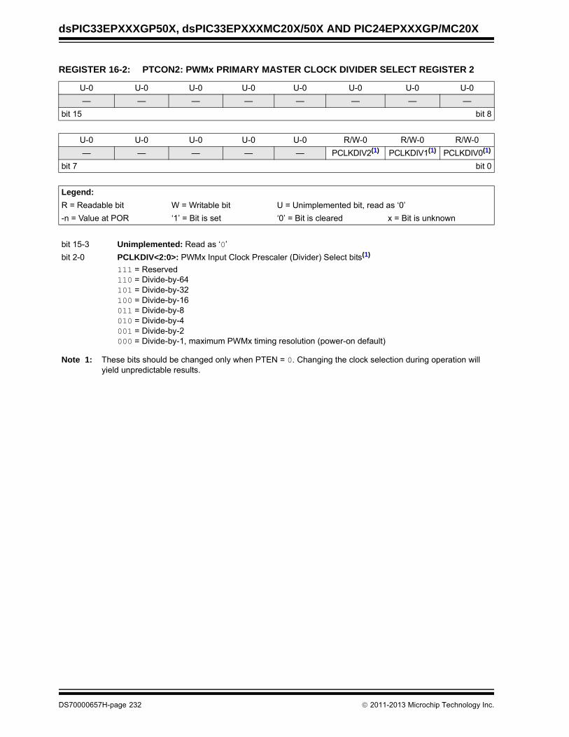
dsPIC33EPXXXGP50X, dsPIC33EPXXXMC20X/50X AND PIC24EPXXXGP/MC20X
REGISTER 16-2: PTCON2: PWMx PRIMARY MASTER CLOCK DIVIDER SELECT REGISTER 2
U-0 U-0 U-0 U-0 U-0 U-0 U-0 U-0
— — — — — — — —
bit 15 bit 8
U-0 U-0 U-0 U-0 U-0 R/W-0 R/W-0 R/W-0
— — — — — PCLKDIV2(1) PCLKDIV1(1) PCLKDIV0(1)
bit 7 bit 0
Legend:
R = Readable bit W = Writable bit U = Unimplemented bit, read as ‘0’
-n = Value at POR ‘1’ = Bit is set ‘0’ = Bit is cleared x = Bit is unknown
bit 15-3 Unimplemented: Read as ‘0’
bit 2-0 PCLKDIV<2:0>: PWMx Input Clock Prescaler (Divider) Select bits(1)
111 = Reserved110 = Divide-by-64101 = Divide-by-32100 = Divide-by-16011 = Divide-by-8010 = Divide-by-4001 = Divide-by-2000 = Divide-by-1, maximum PWMx timing resolution (power-on default)
Note 1: These bits should be changed only when PTEN = 0. Changing the clock selection during operation will yield unpredictable results.
DS70000657H-page 232 2011-2013 Microchip Technology Inc.
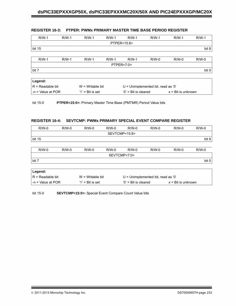
dsPIC33EPXXXGP50X, dsPIC33EPXXXMC20X/50X AND PIC24EPXXXGP/MC20X
REGISTER 16-3: PTPER: PWMx PRIMARY MASTER TIME BASE PERIOD REGISTER
R/W-1 R/W-1 R/W-1 R/W-1 R/W-1 R/W-1 R/W-1 R/W-1
PTPER<15:8>
bit 15 bit 8
R/W-1 R/W-1 R/W-1 R/W-1 R/W-1 R/W-0 R/W-0 R/W-0
PTPER<7:0>
bit 7 bit 0
Legend:
R = Readable bit W = Writable bit U = Unimplemented bit, read as ‘0’
-n = Value at POR ‘1’ = Bit is set ‘0’ = Bit is cleared x = Bit is unknown
bit 15-0 PTPER<15:0>: Primary Master Time Base (PMTMR) Period Value bits
REGISTER 16-4: SEVTCMP: PWMx PRIMARY SPECIAL EVENT COMPARE REGISTER
R/W-0 R/W-0 R/W-0 R/W-0 R/W-0 R/W-0 R/W-0 R/W-0
SEVTCMP<15:8>
bit 15 bit 8
R/W-0 R/W-0 R/W-0 R/W-0 R/W-0 R/W-0 R/W-0 R/W-0
SEVTCMP<7:0>
bit 7 bit 0
Legend:
R = Readable bit W = Writable bit U = Unimplemented bit, read as ‘0’
-n = Value at POR ‘1’ = Bit is set ‘0’ = Bit is cleared x = Bit is unknown
bit 15-0 SEVTCMP<15:0>: Special Event Compare Count Value bits
2011-2013 Microchip Technology Inc. DS70000657H-page 233

dsPIC33EPXXXGP50X, dsPIC33EPXXXMC20X/50X AND PIC24EPXXXGP/MC20X
REGISTER 16-5: CHOP: PWMx CHOP CLOCK GENERATOR REGISTER
R/W-0 U-0 U-0 U-0 U-0 U-0 R/W-0 R/W-0
CHPCLKEN — — — — — CHOPCLK<9:8>
bit 15 bit 8
R/W-0 R/W-0 R/W-0 R/W-0 R/W-0 R/W-0 R/W-0 R/W-0
CHOPCLK<7:0>
bit 7 bit 0
Legend:
R = Readable bit W = Writable bit U = Unimplemented bit, read as ‘0’
-n = Value at POR ‘1’ = Bit is set ‘0’ = Bit is cleared x = Bit is unknown
bit 15 CHPCLKEN: Enable Chop Clock Generator bit
1 = Chop clock generator is enabled0 = Chop clock generator is disabled
bit 14-10 Unimplemented: Read as ‘0’
bit 9-0 CHOPCLK<9:0>: Chop Clock Divider bits
The frequency of the chop clock signal is given by the following expression:Chop Frequency = (FP/PCLKDIV<2:0)/(CHOPCLK<9:0> + 1)
REGISTER 16-6: MDC: PWMx MASTER DUTY CYCLE REGISTER
R/W-0 R/W-0 R/W-0 R/W-0 R/W-0 R/W-0 R/W-0 R/W-0
MDC<15:8>
bit 15 bit 8
R/W-0 R/W-0 R/W-0 R/W-0 R/W-0 R/W-0 R/W-0 R/W-0
MDC<7:0>
bit 7 bit 0
Legend:
R = Readable bit W = Writable bit U = Unimplemented bit, read as ‘0’
-n = Value at POR ‘1’ = Bit is set ‘0’ = Bit is cleared x = Bit is unknown
bit 15-0 MDC<15:0>: PWMx Master Duty Cycle Value bits
DS70000657H-page 234 2011-2013 Microchip Technology Inc.

dsPIC33EPXXXGP50X, dsPIC33EPXXXMC20X/50X AND PIC24EPXXXGP/MC20X
REGISTER 16-7: PWMCONx: PWMx CONTROL REGISTER
HS/HC-0 HS/HC-0 HS/HC-0 R/W-0 R/W-0 R/W-0 R/W-0 R/W-0
FLTSTAT(1) CLSTAT(1) TRGSTAT FLTIEN CLIEN TRGIEN ITB(2) MDCS(2)
bit 15 bit 8
R/W-0 R/W-0 R/W-0 U-0 R/W-0 R/W-0 R/W-0 R/W-0
DTC1 DTC0 DTCP(3) — MTBS CAM(2,4) XPRES(5) IUE(2)
bit 7 bit 0
Legend: HC = Hardware Clearable bit HS = Hardware Settable bit
R = Readable bit W = Writable bit U = Unimplemented bit, read as ‘0’
-n = Value at POR ‘1’ = Bit is set ‘0’ = Bit is cleared x = Bit is unknown
bit 15 FLTSTAT: Fault Interrupt Status bit(1)
1 = Fault interrupt is pending0 = No Fault interrupt is pendingThis bit is cleared by setting FLTIEN = 0.
bit 14 CLSTAT: Current-Limit Interrupt Status bit(1)
1 = Current-limit interrupt is pending0 = No current-limit interrupt is pendingThis bit is cleared by setting CLIEN = 0.
bit 13 TRGSTAT: Trigger Interrupt Status bit
1 = Trigger interrupt is pending0 = No trigger interrupt is pendingThis bit is cleared by setting TRGIEN = 0.
bit 12 FLTIEN: Fault Interrupt Enable bit
1 = Fault interrupt is enabled0 = Fault interrupt is disabled and the FLTSTAT bit is cleared
bit 11 CLIEN: Current-Limit Interrupt Enable bit
1 = Current-limit interrupt is enabled0 = Current-limit interrupt is disabled and the CLSTAT bit is cleared
bit 10 TRGIEN: Trigger Interrupt Enable bit
1 = A trigger event generates an interrupt request0 = Trigger event interrupts are disabled and the TRGSTAT bit is cleared
bit 9 ITB: Independent Time Base Mode bit(2)
1 = PHASEx register provides time base period for this PWM generator0 = PTPER register provides timing for this PWM generator
bit 8 MDCS: Master Duty Cycle Register Select bit(2)
1 = MDC register provides duty cycle information for this PWM generator0 = PDCx register provides duty cycle information for this PWM generator
Note 1: Software must clear the interrupt status here and in the corresponding IFSx bit in the interrupt controller.
2: These bits should not be changed after the PWMx is enabled (PTEN = 1).
3: DTC<1:0> = 11 for DTCP to be effective; otherwise, DTCP is ignored.
4: The Independent Time Base (ITB = 1) mode must be enabled to use Center-Aligned mode. If ITB = 0, the CAM bit is ignored.
5: To operate in External Period Reset mode, the ITB bit must be ‘1’ and the CLMOD bit in the FCLCONx register must be ‘0’.
2011-2013 Microchip Technology Inc. DS70000657H-page 235

dsPIC33EPXXXGP50X, dsPIC33EPXXXMC20X/50X AND PIC24EPXXXGP/MC20X
bit 7-6 DTC<1:0>: Dead-Time Control bits
11 = Dead-Time Compensation mode10 = Dead-time function is disabled01 = Negative dead time is actively applied for Complementary Output mode00 = Positive dead time is actively applied for all output modes
bit 5 DTCP: Dead-Time Compensation Polarity bit(3)
When Set to ‘1’:If DTCMPx = 0, PWMxL is shortened and PWMxH is lengthened.If DTCMPx = 1, PWMxH is shortened and PWMxL is lengthened.
When Set to ‘0’:If DTCMPx = 0, PWMxH is shortened and PWMxL is lengthened.If DTCMPx = 1, PWMxL is shortened and PWMxH is lengthened.
bit 4 Unimplemented: Read as ‘0’
bit 3 MTBS: Master Time Base Select bit
1 = PWM generator uses the secondary master time base for synchronization and as the clock sourcefor the PWM generation logic (if secondary time base is available)
0 = PWM generator uses the primary master time base for synchronization and as the clock sourcefor the PWM generation logic
bit 2 CAM: Center-Aligned Mode Enable bit(2,4)
1 = Center-Aligned mode is enabled0 = Edge-Aligned mode is enabled
bit 1 XPRES: External PWMx Reset Control bit(5)
1 = Current-limit source resets the time base for this PWM generator if it is in Independent Time Basemode
0 = External pins do not affect PWMx time base
bit 0 IUE: Immediate Update Enable bit(2)
1 = Updates to the active MDC/PDCx/DTRx/ALTDTRx/PHASEx registers are immediate0 = Updates to the active MDC/PDCx/DTRx/ALTDTRx/PHASEx registers are synchronized to the
PWMx period boundary
REGISTER 16-7: PWMCONx: PWMx CONTROL REGISTER (CONTINUED)
Note 1: Software must clear the interrupt status here and in the corresponding IFSx bit in the interrupt controller.
2: These bits should not be changed after the PWMx is enabled (PTEN = 1).
3: DTC<1:0> = 11 for DTCP to be effective; otherwise, DTCP is ignored.
4: The Independent Time Base (ITB = 1) mode must be enabled to use Center-Aligned mode. If ITB = 0, the CAM bit is ignored.
5: To operate in External Period Reset mode, the ITB bit must be ‘1’ and the CLMOD bit in the FCLCONx register must be ‘0’.
DS70000657H-page 236 2011-2013 Microchip Technology Inc.

dsPIC33EPXXXGP50X, dsPIC33EPXXXMC20X/50X AND PIC24EPXXXGP/MC20X
REGISTER 16-8: PDCx: PWMx GENERATOR DUTY CYCLE REGISTER
R/W-0 R/W-0 R/W-0 R/W-0 R/W-0 R/W-0 R/W-0 R/W-0
PDCx<15:8>
bit 15 bit 8
R/W-0 R/W-0 R/W-0 R/W-0 R/W-0 R/W-0 R/W-0 R/W-0
PDCx<7:0>
bit 7 bit 0
Legend:
R = Readable bit W = Writable bit U = Unimplemented bit, read as ‘0’
-n = Value at POR ‘1’ = Bit is set ‘0’ = Bit is cleared x = Bit is unknown
bit 15-0 PDCx<15:0>: PWMx Generator # Duty Cycle Value bits
REGISTER 16-9: PHASEx: PWMx PRIMARY PHASE-SHIFT REGISTER
R/W-0 R/W-0 R/W-0 R/W-0 R/W-0 R/W-0 R/W-0 R/W-0
PHASEx<15:8>
bit 15 bit 8
R/W-0 R/W-0 R/W-0 R/W-0 R/W-0 R/W-0 R/W-0 R/W-0
PHASEx<7:0>
bit 7 bit 0
Legend:
R = Readable bit W = Writable bit U = Unimplemented bit, read as ‘0’
-n = Value at POR ‘1’ = Bit is set ‘0’ = Bit is cleared x = Bit is unknown
bit 15-0 PHASEx<15:0>: PWMx Phase-Shift Value or Independent Time Base Period for the PWM Generator bits
Note 1: If ITB (PWMCONx<9>) = 0, the following applies based on the mode of operation:Complementary, Redundant and Push-Pull Output mode (PMOD<1:0> (IOCON<11:10>) = 00, 01 or 10),PHASEx<15:0> = Phase-shift value for PWMxH and PWMxL outputs
2: If ITB (PWMCONx<9>) = 1, the following applies based on the mode of operation:Complementary, Redundant and Push-Pull Output mode (PMOD<1:0> (IOCONx<11:10>) = 00, 01 or 10),PHASEx<15:0> = Independent time base period value for PWMxH and PWMxL
2011-2013 Microchip Technology Inc. DS70000657H-page 237

dsPIC33EPXXXGP50X, dsPIC33EPXXXMC20X/50X AND PIC24EPXXXGP/MC20X
REGISTER 16-10: DTRx: PWMx DEAD-TIME REGISTER
U-0 U-0 R/W-0 R/W-0 R/W-0 R/W-0 R/W-0 R/W-0
— — DTRx<13:8>
bit 15 bit 8
R/W-0 R/W-0 R/W-0 R/W-0 R/W-0 R/W-0 R/W-0 R/W-0
DTRx<7:0>
bit 7 bit 0
Legend:
R = Readable bit W = Writable bit U = Unimplemented bit, read as ‘0’
-n = Value at POR ‘1’ = Bit is set ‘0’ = Bit is cleared x = Bit is unknown
bit 15-14 Unimplemented: Read as ‘0’
bit 13-0 DTRx<13:0>: Unsigned 14-Bit Dead-Time Value for PWMx Dead-Time Unit bits
REGISTER 16-11: ALTDTRx: PWMx ALTERNATE DEAD-TIME REGISTER
U-0 U-0 R/W-0 R/W-0 R/W-0 R/W-0 R/W-0 R/W-0
— — ALTDTRx<13:8>
bit 15 bit 8
R/W-0 R/W-0 R/W-0 R/W-0 R/W-0 R/W-0 R/W-0 R/W-0
ALTDTRx<7:0>
bit 7 bit 0
Legend:
R = Readable bit W = Writable bit U = Unimplemented bit, read as ‘0’
-n = Value at POR ‘1’ = Bit is set ‘0’ = Bit is cleared x = Bit is unknown
bit 15-14 Unimplemented: Read as ‘0’
bit 13-0 ALTDTRx<13:0>: Unsigned 14-Bit Dead-Time Value for PWMx Dead-Time Unit bits
DS70000657H-page 238 2011-2013 Microchip Technology Inc.

dsPIC33EPXXXGP50X, dsPIC33EPXXXMC20X/50X AND PIC24EPXXXGP/MC20X
REGISTER 16-12: TRGCONx: PWMx TRIGGER CONTROL REGISTER
R/W-0 R/W-0 R/W-0 R/W-0 U-0 U-0 U-0 U-0
TRGDIV<3:0> — — — —
bit 15 bit 8
U-0 U-0 R/W-0 R/W-0 R/W-0 R/W-0 R/W-0 R/W-0
— — TRGSTRT<5:0>(1)
bit 7 bit 0
Legend:
R = Readable bit W = Writable bit U = Unimplemented bit, read as ‘0’
-n = Value at POR ‘1’ = Bit is set ‘0’ = Bit is cleared x = Bit is unknown
bit 15-12 TRGDIV<3:0>: Trigger # Output Divider bits
1111 = Trigger output for every 16th trigger event1110 = Trigger output for every 15th trigger event1101 = Trigger output for every 14th trigger event1100 = Trigger output for every 13th trigger event1011 = Trigger output for every 12th trigger event1010 = Trigger output for every 11th trigger event1001 = Trigger output for every 10th trigger event1000 = Trigger output for every 9th trigger event0111 = Trigger output for every 8th trigger event0110 = Trigger output for every 7th trigger event0101 = Trigger output for every 6th trigger event0100 = Trigger output for every 5th trigger event0011 = Trigger output for every 4th trigger event0010 = Trigger output for every 3rd trigger event0001 = Trigger output for every 2nd trigger event0000 = Trigger output for every trigger event
bit 11-6 Unimplemented: Read as ‘0’
bit 5-0 TRGSTRT<5:0>: Trigger Postscaler Start Enable Select bits(1)
111111 = Waits 63 PWM cycles before generating the first trigger event after the module is enabled
•
•
•
000010 = Waits 2 PWM cycles before generating the first trigger event after the module is enabled000001 = Waits 1 PWM cycle before generating the first trigger event after the module is enabled000000 = Waits 0 PWM cycles before generating the first trigger event after the module is enabled
Note 1: The secondary PWM generator cannot generate PWMx trigger interrupts.
2011-2013 Microchip Technology Inc. DS70000657H-page 239
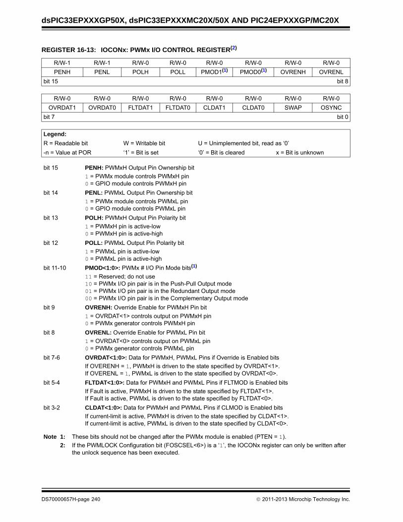
dsPIC33EPXXXGP50X, dsPIC33EPXXXMC20X/50X AND PIC24EPXXXGP/MC20X
REGISTER 16-13: IOCONx: PWMx I/O CONTROL REGISTER(2)
R/W-1 R/W-1 R/W-0 R/W-0 R/W-0 R/W-0 R/W-0 R/W-0
PENH PENL POLH POLL PMOD1(1) PMOD0(1) OVRENH OVRENL
bit 15 bit 8
R/W-0 R/W-0 R/W-0 R/W-0 R/W-0 R/W-0 R/W-0 R/W-0
OVRDAT1 OVRDAT0 FLTDAT1 FLTDAT0 CLDAT1 CLDAT0 SWAP OSYNC
bit 7 bit 0
Legend:
R = Readable bit W = Writable bit U = Unimplemented bit, read as ‘0’
-n = Value at POR ‘1’ = Bit is set ‘0’ = Bit is cleared x = Bit is unknown
bit 15 PENH: PWMxH Output Pin Ownership bit
1 = PWMx module controls PWMxH pin0 = GPIO module controls PWMxH pin
bit 14 PENL: PWMxL Output Pin Ownership bit
1 = PWMx module controls PWMxL pin0 = GPIO module controls PWMxL pin
bit 13 POLH: PWMxH Output Pin Polarity bit
1 = PWMxH pin is active-low0 = PWMxH pin is active-high
bit 12 POLL: PWMxL Output Pin Polarity bit
1 = PWMxL pin is active-low0 = PWMxL pin is active-high
bit 11-10 PMOD<1:0>: PWMx # I/O Pin Mode bits(1)
11 = Reserved; do not use10 = PWMx I/O pin pair is in the Push-Pull Output mode01 = PWMx I/O pin pair is in the Redundant Output mode00 = PWMx I/O pin pair is in the Complementary Output mode
bit 9 OVRENH: Override Enable for PWMxH Pin bit
1 = OVRDAT<1> controls output on PWMxH pin0 = PWMx generator controls PWMxH pin
bit 8 OVRENL: Override Enable for PWMxL Pin bit
1 = OVRDAT<0> controls output on PWMxL pin0 = PWMx generator controls PWMxL pin
bit 7-6 OVRDAT<1:0>: Data for PWMxH, PWMxL Pins if Override is Enabled bits
If OVERENH = 1, PWMxH is driven to the state specified by OVRDAT<1>.If OVERENL = 1, PWMxL is driven to the state specified by OVRDAT<0>.
bit 5-4 FLTDAT<1:0>: Data for PWMxH and PWMxL Pins if FLTMOD is Enabled bits
If Fault is active, PWMxH is driven to the state specified by FLTDAT<1>.If Fault is active, PWMxL is driven to the state specified by FLTDAT<0>.
bit 3-2 CLDAT<1:0>: Data for PWMxH and PWMxL Pins if CLMOD is Enabled bits
If current-limit is active, PWMxH is driven to the state specified by CLDAT<1>.If current-limit is active, PWMxL is driven to the state specified by CLDAT<0>.
Note 1: These bits should not be changed after the PWMx module is enabled (PTEN = 1).
2: If the PWMLOCK Configuration bit (FOSCSEL<6>) is a ‘1’, the IOCONx register can only be written after the unlock sequence has been executed.
DS70000657H-page 240 2011-2013 Microchip Technology Inc.
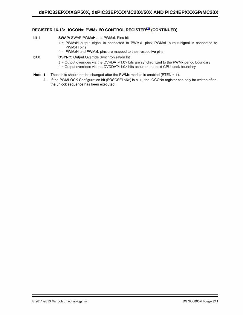
dsPIC33EPXXXGP50X, dsPIC33EPXXXMC20X/50X AND PIC24EPXXXGP/MC20X
bit 1 SWAP: SWAP PWMxH and PWMxL Pins bit
1 = PWMxH output signal is connected to PWMxL pins; PWMxL output signal is connected toPWMxH pins
0 = PWMxH and PWMxL pins are mapped to their respective pins
bit 0 OSYNC: Output Override Synchronization bit
1 = Output overrides via the OVRDAT<1:0> bits are synchronized to the PWMx period boundary0 = Output overrides via the OVDDAT<1:0> bits occur on the next CPU clock boundary
REGISTER 16-13: IOCONx: PWMx I/O CONTROL REGISTER(2) (CONTINUED)
Note 1: These bits should not be changed after the PWMx module is enabled (PTEN = 1).
2: If the PWMLOCK Configuration bit (FOSCSEL<6>) is a ‘1’, the IOCONx register can only be written after the unlock sequence has been executed.
2011-2013 Microchip Technology Inc. DS70000657H-page 241

dsPIC33EPXXXGP50X, dsPIC33EPXXXMC20X/50X AND PIC24EPXXXGP/MC20X
REGISTER 16-14: TRIGx: PWMx PRIMARY TRIGGER COMPARE VALUE REGISTER
R/W-0 R/W-0 R/W-0 R/W-0 R/W-0 R/W-0 R/W-0 R/W-0
TRGCMP<15:8>
bit 15 bit 8
R/W-0 R/W-0 R/W-0 R/W-0 R/W-0 R/W-0 R/W-0 R/W-0
TRGCMP<7:0>
bit 7 bit 0
Legend:
R = Readable bit W = Writable bit U = Unimplemented bit, read as ‘0’
-n = Value at POR ‘1’ = Bit is set ‘0’ = Bit is cleared x = Bit is unknown
bit 15-0 TRGCMP<15:0>: Trigger Control Value bits
When the primary PWMx functions in local time base, this register contains the compare values that can trigger the ADC module.
DS70000657H-page 242 2011-2013 Microchip Technology Inc.

dsPIC33EPXXXGP50X, dsPIC33EPXXXMC20X/50X AND PIC24EPXXXGP/MC20X
REGISTER 16-15: FCLCONx: PWMx FAULT CURRENT-LIMIT CONTROL REGISTER(1)
U-0 R/W-0 R/W-0 R/W-0 R/W-0 R/W-0 R/W-0 R/W-0
— CLSRC4 CLSRC3 CLSRC2 CLSRC1 CLSRC0 CLPOL(2) CLMOD
bit 15 bit 8
R/W-1 R/W-1 R/W-1 R/W-1 R/W-1 R/W-0 R/W-0 R/W-0
FLTSRC4 FLTSRC3 FLTSRC2 FLTSRC1 FLTSRC0 FLTPOL(2) FLTMOD1 FLTMOD0
bit 7 bit 0
Legend:
R = Readable bit W = Writable bit U = Unimplemented bit, read as ‘0’
-n = Value at POR ‘1’ = Bit is set ‘0’ = Bit is cleared x = Bit is unknown
bit 15 Unimplemented: Read as ‘0’
bit 14-10 CLSRC<4:0>: Current-Limit Control Signal Source Select for PWM Generator # bits
11111 = Fault 3211110 = Reserved•••
01100 = Reserved01011 = Comparator 401010 = Op Amp/Comparator 301001 = Op Amp/Comparator 201000 = Op Amp/Comparator 100111 = Reserved00110 = Reserved00101 = Reserved00100 = Reserved00011 = Fault 400010 = Fault 300001 = Fault 200000 = Fault 1 (default)
bit 9 CLPOL: Current-Limit Polarity for PWM Generator # bit(2)
1 = The selected current-limit source is active-low0 = The selected current-limit source is active-high
bit 8 CLMOD: Current-Limit Mode Enable for PWM Generator # bit
1 = Current-Limit mode is enabled0 = Current-Limit mode is disabled
Note 1: If the PWMLOCK Configuration bit (FOSCSEL<6>) is a ‘1’, the IOCONx register can only be written after the unlock sequence has been executed.
2: These bits should be changed only when PTEN = 0. Changing the clock selection during operation will yield unpredictable results.
2011-2013 Microchip Technology Inc. DS70000657H-page 243
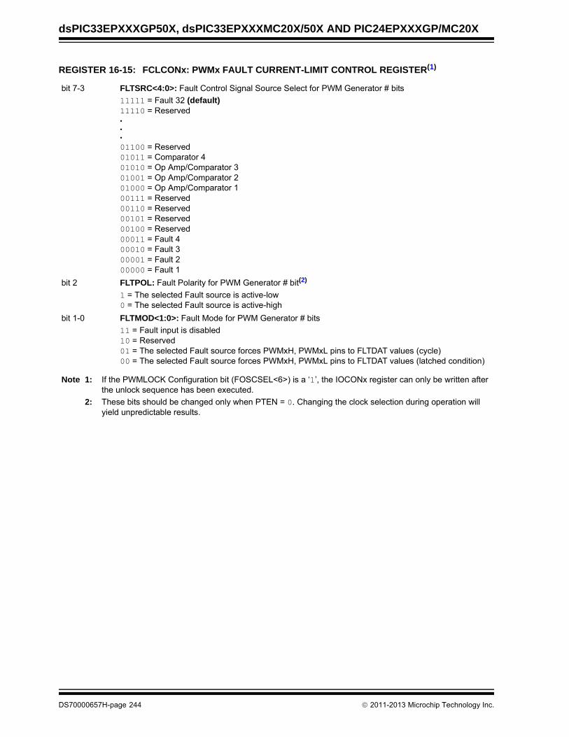
dsPIC33EPXXXGP50X, dsPIC33EPXXXMC20X/50X AND PIC24EPXXXGP/MC20X
bit 7-3 FLTSRC<4:0>: Fault Control Signal Source Select for PWM Generator # bits
11111 = Fault 32 (default)11110 = Reserved•••
01100 = Reserved01011 = Comparator 401010 = Op Amp/Comparator 301001 = Op Amp/Comparator 201000 = Op Amp/Comparator 100111 = Reserved00110 = Reserved00101 = Reserved00100 = Reserved00011 = Fault 400010 = Fault 300001 = Fault 200000 = Fault 1
bit 2 FLTPOL: Fault Polarity for PWM Generator # bit(2)
1 = The selected Fault source is active-low0 = The selected Fault source is active-high
bit 1-0 FLTMOD<1:0>: Fault Mode for PWM Generator # bits
11 = Fault input is disabled10 = Reserved01 = The selected Fault source forces PWMxH, PWMxL pins to FLTDAT values (cycle)00 = The selected Fault source forces PWMxH, PWMxL pins to FLTDAT values (latched condition)
REGISTER 16-15: FCLCONx: PWMx FAULT CURRENT-LIMIT CONTROL REGISTER(1)
Note 1: If the PWMLOCK Configuration bit (FOSCSEL<6>) is a ‘1’, the IOCONx register can only be written after the unlock sequence has been executed.
2: These bits should be changed only when PTEN = 0. Changing the clock selection during operation will yield unpredictable results.
DS70000657H-page 244 2011-2013 Microchip Technology Inc.
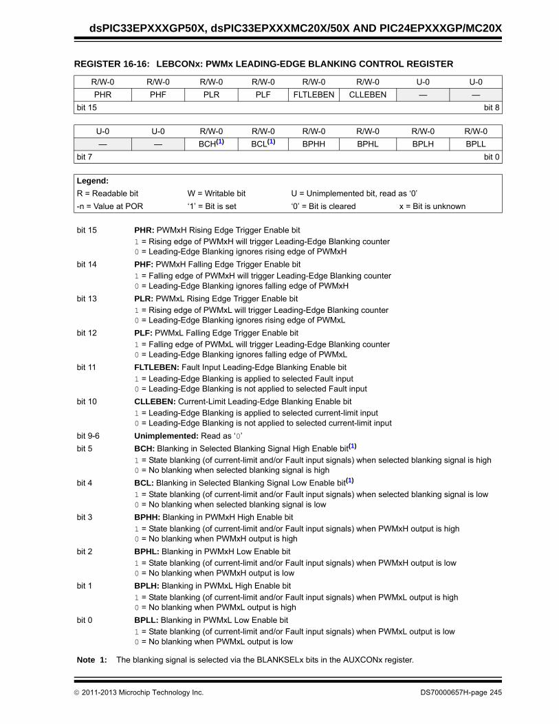
dsPIC33EPXXXGP50X, dsPIC33EPXXXMC20X/50X AND PIC24EPXXXGP/MC20X
REGISTER 16-16: LEBCONx: PWMx LEADING-EDGE BLANKING CONTROL REGISTER
R/W-0 R/W-0 R/W-0 R/W-0 R/W-0 R/W-0 U-0 U-0
PHR PHF PLR PLF FLTLEBEN CLLEBEN — —
bit 15 bit 8
U-0 U-0 R/W-0 R/W-0 R/W-0 R/W-0 R/W-0 R/W-0
— — BCH(1) BCL(1) BPHH BPHL BPLH BPLL
bit 7 bit 0
Legend:
R = Readable bit W = Writable bit U = Unimplemented bit, read as ‘0’
-n = Value at POR ‘1’ = Bit is set ‘0’ = Bit is cleared x = Bit is unknown
bit 15 PHR: PWMxH Rising Edge Trigger Enable bit1 = Rising edge of PWMxH will trigger Leading-Edge Blanking counter0 = Leading-Edge Blanking ignores rising edge of PWMxH
bit 14 PHF: PWMxH Falling Edge Trigger Enable bit1 = Falling edge of PWMxH will trigger Leading-Edge Blanking counter0 = Leading-Edge Blanking ignores falling edge of PWMxH
bit 13 PLR: PWMxL Rising Edge Trigger Enable bit1 = Rising edge of PWMxL will trigger Leading-Edge Blanking counter0 = Leading-Edge Blanking ignores rising edge of PWMxL
bit 12 PLF: PWMxL Falling Edge Trigger Enable bit1 = Falling edge of PWMxL will trigger Leading-Edge Blanking counter0 = Leading-Edge Blanking ignores falling edge of PWMxL
bit 11 FLTLEBEN: Fault Input Leading-Edge Blanking Enable bit1 = Leading-Edge Blanking is applied to selected Fault input0 = Leading-Edge Blanking is not applied to selected Fault input
bit 10 CLLEBEN: Current-Limit Leading-Edge Blanking Enable bit1 = Leading-Edge Blanking is applied to selected current-limit input0 = Leading-Edge Blanking is not applied to selected current-limit input
bit 9-6 Unimplemented: Read as ‘0’
bit 5 BCH: Blanking in Selected Blanking Signal High Enable bit(1)
1 = State blanking (of current-limit and/or Fault input signals) when selected blanking signal is high0 = No blanking when selected blanking signal is high
bit 4 BCL: Blanking in Selected Blanking Signal Low Enable bit(1)
1 = State blanking (of current-limit and/or Fault input signals) when selected blanking signal is low0 = No blanking when selected blanking signal is low
bit 3 BPHH: Blanking in PWMxH High Enable bit
1 = State blanking (of current-limit and/or Fault input signals) when PWMxH output is high0 = No blanking when PWMxH output is high
bit 2 BPHL: Blanking in PWMxH Low Enable bit1 = State blanking (of current-limit and/or Fault input signals) when PWMxH output is low0 = No blanking when PWMxH output is low
bit 1 BPLH: Blanking in PWMxL High Enable bit
1 = State blanking (of current-limit and/or Fault input signals) when PWMxL output is high0 = No blanking when PWMxL output is high
bit 0 BPLL: Blanking in PWMxL Low Enable bit1 = State blanking (of current-limit and/or Fault input signals) when PWMxL output is low0 = No blanking when PWMxL output is low
Note 1: The blanking signal is selected via the BLANKSELx bits in the AUXCONx register.
2011-2013 Microchip Technology Inc. DS70000657H-page 245

dsPIC33EPXXXGP50X, dsPIC33EPXXXMC20X/50X AND PIC24EPXXXGP/MC20X
REGISTER 16-17: LEBDLYx: PWMx LEADING-EDGE BLANKING DELAY REGISTER
U-0 U-0 U-0 U-0 R/W-0 R/W-0 R/W-0 R/W-0
— — — — LEB<11:8>
bit 15 bit 8
R/W-0 R/W-0 R/W-0 R/W-0 R/W-0 R/W-0 R/W-0 R/W-0
LEB<7:0>
bit 7 bit 0
Legend:
R = Readable bit W = Writable bit U = Unimplemented bit, read as ‘0’
-n = Value at POR ‘1’ = Bit is set ‘0’ = Bit is cleared x = Bit is unknown
bit 15-12 Unimplemented: Read as ‘0’
bit 11-0 LEB<11:0>: Leading-Edge Blanking Delay for Current-Limit and Fault Inputs bits
DS70000657H-page 246 2011-2013 Microchip Technology Inc.

dsPIC33EPXXXGP50X, dsPIC33EPXXXMC20X/50X AND PIC24EPXXXGP/MC20X
REGISTER 16-18: AUXCONx: PWMx AUXILIARY CONTROL REGISTER
U-0 U-0 U-0 U-0 R/W-0 R/W-0 R/W-0 R/W-0
— — — — BLANKSEL3 BLANKSEL2 BLANKSEL1 BLANKSEL0
bit 15 bit 8
U-0 U-0 R/W-0 R/W-0 R/W-0 R/W-0 R/W-0 R/W-0
— — CHOPSEL3 CHOPSEL2 CHOPSEL1 CHOPSEL0 CHOPHEN CHOPLEN
bit 7 bit 0
Legend:
R = Readable bit W = Writable bit U = Unimplemented bit, read as ‘0’
-n = Value at POR ‘1’ = Bit is set ‘0’ = Bit is cleared x = Bit is unknown
bit 15-12 Unimplemented: Read as ‘0’
bit 11-8 BLANKSEL<3:0>: PWMx State Blank Source Select bits
The selected state blank signal will block the current-limit and/or Fault input signals (if enabled via theBCH and BCL bits in the LEBCONx register).1001 = Reserved
•
•
•
0100 = Reserved0011 = PWM3H selected as state blank source0010 = PWM2H selected as state blank source0001 = PWM1H selected as state blank source0000 = No state blanking
bit 7-6 Unimplemented: Read as ‘0’
bit 5-2 CHOPSEL<3:0>: PWMx Chop Clock Source Select bits
The selected signal will enable and disable (CHOP) the selected PWMx outputs.1001 = Reserved
•
•
•
0100 = Reserved0011 = PWM3H selected as CHOP clock source0010 = PWM2H selected as CHOP clock source0001 = PWM1H selected as CHOP clock source0000 = Chop clock generator selected as CHOP clock source
bit 1 CHOPHEN: PWMxH Output Chopping Enable bit
1 = PWMxH chopping function is enabled0 = PWMxH chopping function is disabled
bit 0 CHOPLEN: PWMxL Output Chopping Enable bit
1 = PWMxL chopping function is enabled0 = PWMxL chopping function is disabled
2011-2013 Microchip Technology Inc. DS70000657H-page 247
dsPIC33EPXXXGP50X, dsPIC33EPXXXMC20X/50X AND PIC24EPXXXGP/MC20X
NOTES:
DS70000657H-page 248 2011-2013 Microchip Technology Inc.
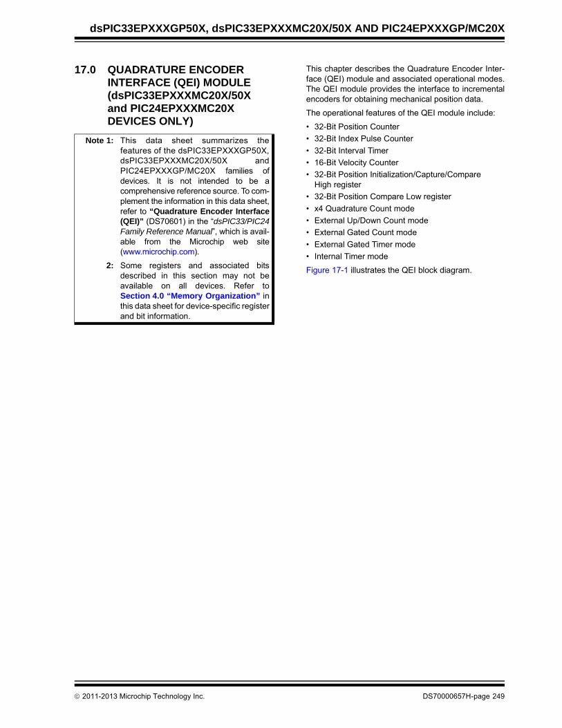
dsPIC33EPXXXGP50X, dsPIC33EPXXXMC20X/50X AND PIC24EPXXXGP/MC20X
17.0 QUADRATURE ENCODER INTERFACE (QEI) MODULE (dsPIC33EPXXXMC20X/50X and PIC24EPXXXMC20X DEVICES ONLY)
This chapter describes the Quadrature Encoder Inter-face (QEI) module and associated operational modes.The QEI module provides the interface to incrementalencoders for obtaining mechanical position data.
The operational features of the QEI module include:
• 32-Bit Position Counter
• 32-Bit Index Pulse Counter
• 32-Bit Interval Timer
• 16-Bit Velocity Counter
• 32-Bit Position Initialization/Capture/Compare High register
• 32-Bit Position Compare Low register
• x4 Quadrature Count mode
• External Up/Down Count mode
• External Gated Count mode
• External Gated Timer mode
• Internal Timer mode
Figure 17-1 illustrates the QEI block diagram.
Note 1: This data sheet summarizes thefeatures of the dsPIC33EPXXXGP50X,dsPIC33EPXXXMC20X/50X andPIC24EPXXXGP/MC20X families ofdevices. It is not intended to be acomprehensive reference source. To com-plement the information in this data sheet,refer to “Quadrature Encoder Interface(QEI)” (DS70601) in the “dsPIC33/PIC24Family Reference Manual”, which is avail-able from the Microchip web site(www.microchip.com).
2: Some registers and associated bitsdescribed in this section may not beavailable on all devices. Refer toSection 4.0 “Memory Organization” inthis data sheet for device-specific registerand bit information.
2011-2013 Microchip Technology Inc. DS70000657H-page 249

ds
PIC
33E
PX
XX
GP
50X
, dsP
IC33
EP
XX
XM
C20
X/5
0X A
ND
PIC
24E
PX
XX
GP
/MC
20X
DS
70
00
06
57
H-p
ag
e 2
50
2
01
1-2
01
3 M
icroch
ip T
ech
no
log
y Inc.
COUNT_EN
32-Bit Greater Than or EqualCompare Register
32-Bit Greater Than
Data Bus
PCHEQ
PCHGE
CNT_DIR
GATEN
0
1
or Equal Comparator
(QEI1GEC)(1)
32-Bit Initialization andCapture Register
(QEI1IC)(1)
CAPEN
ster
FIGURE 17-1: QEI BLOCK DIAGRAM
QuadratureDecoder
Logic
CNTCMPx
QEBx
QEAx
INDXx
COUNT
DIR
FP COUNT
32-Bit Index Counter Register
DigitalFilter
HOMEx FHOMEx
Data Bus
COUNT_EN
CNT_DIRCNT_DIR
FINDXx
FINDXx
32-Bit Interval Timer16-Bit Index CounterHold Register
32-Bit IntervalTimer Register
Hold Register
COUNT_EN
FP
EXTCNT
EXTCNT
DIR_GATE
16-Bit Velocity
COUNT_ENCNT_DIR
Counter Register
PCLLE
PCHGE
DIVCLK
DIR
DIR_GATE
1’b0
PCLLE
CNTPOL
DIR_GATE
DIVCLK
32-Bit Less Than
PCLLE
or Equal Comparator
PCLEQPCHGE
QFDIV
CCM
INTDIV
(VEL1CNT)
(INT1TMR)
(INT1HLD)
(INDX1CNT)
(INDX1HLD)
INDX1CNTLINDX1CNTHPOS1CNTLPOS1CNTH
32-Bit Less Than or EqualCompare Register
(QEI1LEC)
16-Bit Position CounterHold Register(POS1HLD)
Q
Note 1: These registers map to the same memory location.
OUTFNC
FLTREN
(POS1CNT)32-Bit Position Counter Regi
dsPIC33EPXXXGP50X, dsPIC33EPXXXMC20X/50X AND PIC24EPXXXGP/MC20X
17.1 QEI Resources
Many useful resources are provided on the main prod-uct page of the Microchip web site for the devices listedin this data sheet. This product page, which can beaccessed using this link, contains the latest updatesand additional information.
17.1.1 KEY RESOURCES
• “Quadrature Encoder Interface” (DS70601) in the “dsPIC33/PIC24 Family Reference Manual”
• Code Samples
• Application Notes
• Software Libraries
• Webinars
• All Related “dsPIC33/PIC24 Family Reference Manual” Sections
• Development Tools
Note: In the event you are not able to access theproduct page using the link above, enterthis URL in your browser:http://www.microchip.com/wwwproducts/Devices.aspx?dDocName=en555464
2011-2013 Microchip Technology Inc. DS70000657H-page 251
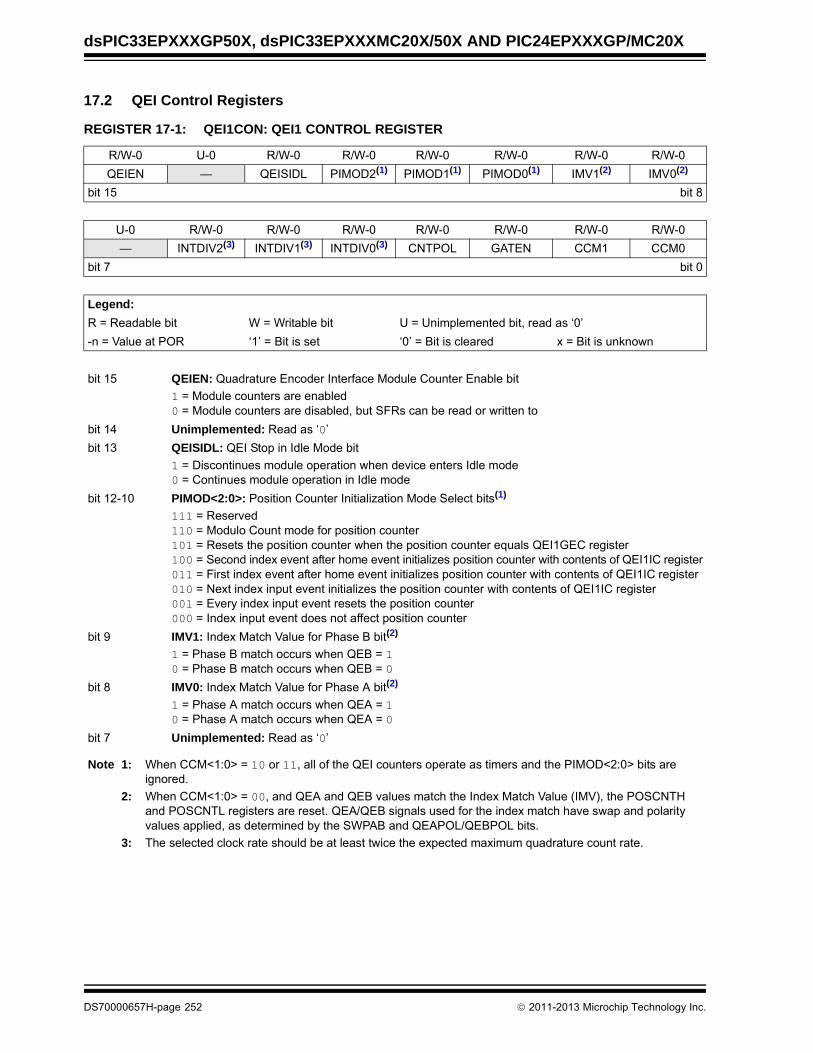
dsPIC33EPXXXGP50X, dsPIC33EPXXXMC20X/50X AND PIC24EPXXXGP/MC20X
17.2 QEI Control Registers
REGISTER 17-1: QEI1CON: QEI1 CONTROL REGISTER
R/W-0 U-0 R/W-0 R/W-0 R/W-0 R/W-0 R/W-0 R/W-0
QEIEN — QEISIDL PIMOD2(1) PIMOD1(1) PIMOD0(1) IMV1(2) IMV0(2)
bit 15 bit 8
U-0 R/W-0 R/W-0 R/W-0 R/W-0 R/W-0 R/W-0 R/W-0
— INTDIV2(3) INTDIV1(3) INTDIV0(3) CNTPOL GATEN CCM1 CCM0
bit 7 bit 0
Legend:
R = Readable bit W = Writable bit U = Unimplemented bit, read as ‘0’
-n = Value at POR ‘1’ = Bit is set ‘0’ = Bit is cleared x = Bit is unknown
bit 15 QEIEN: Quadrature Encoder Interface Module Counter Enable bit
1 = Module counters are enabled0 = Module counters are disabled, but SFRs can be read or written to
bit 14 Unimplemented: Read as ‘0’
bit 13 QEISIDL: QEI Stop in Idle Mode bit
1 = Discontinues module operation when device enters Idle mode0 = Continues module operation in Idle mode
bit 12-10 PIMOD<2:0>: Position Counter Initialization Mode Select bits(1)
111 = Reserved110 = Modulo Count mode for position counter101 = Resets the position counter when the position counter equals QEI1GEC register 100 = Second index event after home event initializes position counter with contents of QEI1IC register011 = First index event after home event initializes position counter with contents of QEI1IC register010 = Next index input event initializes the position counter with contents of QEI1IC register001 = Every index input event resets the position counter000 = Index input event does not affect position counter
bit 9 IMV1: Index Match Value for Phase B bit(2)
1 = Phase B match occurs when QEB = 10 = Phase B match occurs when QEB = 0
bit 8 IMV0: Index Match Value for Phase A bit(2)
1 = Phase A match occurs when QEA = 10 = Phase A match occurs when QEA = 0
bit 7 Unimplemented: Read as ‘0’
Note 1: When CCM<1:0> = 10 or 11, all of the QEI counters operate as timers and the PIMOD<2:0> bits are ignored.
2: When CCM<1:0> = 00, and QEA and QEB values match the Index Match Value (IMV), the POSCNTH and POSCNTL registers are reset. QEA/QEB signals used for the index match have swap and polarity values applied, as determined by the SWPAB and QEAPOL/QEBPOL bits.
3: The selected clock rate should be at least twice the expected maximum quadrature count rate.
DS70000657H-page 252 2011-2013 Microchip Technology Inc.

dsPIC33EPXXXGP50X, dsPIC33EPXXXMC20X/50X AND PIC24EPXXXGP/MC20X
bit 6-4 INTDIV<2:0>: Timer Input Clock Prescale Select bits (interval timer, main timer (position counter),velocity counter and index counter internal clock divider select)(3)
111 = 1:128 prescale value110 = 1:64 prescale value101 = 1:32 prescale value100 = 1:16 prescale value011 = 1:8 prescale value010 = 1:4 prescale value001 = 1:2 prescale value000 = 1:1 prescale value
bit 3 CNTPOL: Position and Index Counter/Timer Direction Select bit
1 = Counter direction is negative unless modified by external up/down signal0 = Counter direction is positive unless modified by external up/down signal
bit 2 GATEN: External Count Gate Enable bit
1 = External gate signal controls position counter operation0 = External gate signal does not affect position counter/timer operation
bit 1-0 CCM<1:0>: Counter Control Mode Selection bits
11 = Internal Timer mode with optional external count is selected10 = External clock count with optional external count is selected01 = External clock count with external up/down direction is selected 00 = Quadrature Encoder Interface (x4 mode) Count mode is selected
REGISTER 17-1: QEI1CON: QEI1 CONTROL REGISTER (CONTINUED)
Note 1: When CCM<1:0> = 10 or 11, all of the QEI counters operate as timers and the PIMOD<2:0> bits are ignored.
2: When CCM<1:0> = 00, and QEA and QEB values match the Index Match Value (IMV), the POSCNTH and POSCNTL registers are reset. QEA/QEB signals used for the index match have swap and polarity values applied, as determined by the SWPAB and QEAPOL/QEBPOL bits.
3: The selected clock rate should be at least twice the expected maximum quadrature count rate.
2011-2013 Microchip Technology Inc. DS70000657H-page 253

dsPIC33EPXXXGP50X, dsPIC33EPXXXMC20X/50X AND PIC24EPXXXGP/MC20X
REGISTER 17-2: QEI1IOC: QEI1 I/O CONTROL REGISTER
R/W-0 R/W-0 R/W-0 R/W-0 R/W-0 R/W-0 R/W-0 R/W-0
QCAPEN FLTREN QFDIV2 QFDIV1 QFDIV0 OUTFNC1 OUTFNC0 SWPAB
bit 15 bit 8
R/W-0 R/W-0 R/W-0 R/W-0 R-x R-x R-x R-x
HOMPOL IDXPOL QEBPOL QEAPOL HOME INDEX QEB QEA
bit 7 bit 0
Legend:
R = Readable bit W = Writable bit U = Unimplemented bit, read as ‘0’
-n = Value at POR ‘1’ = Bit is set ‘0’ = Bit is cleared x = Bit is unknown
bit 15 QCAPEN: QEI Position Counter Input Capture Enable bit
1 = Index match event triggers a position capture event0 = Index match event does not trigger a position capture event
bit 14 FLTREN: QEAx/QEBx/INDXx/HOMEx Digital Filter Enable bit
1 = Input pin digital filter is enabled0 = Input pin digital filter is disabled (bypassed)
bit 13-11 QFDIV<2:0>: QEAx/QEBx/INDXx/HOMEx Digital Input Filter Clock Divide Select bits
111 = 1:128 clock divide110 = 1:64 clock divide101 = 1:32 clock divide100 = 1:16 clock divide011 = 1:8 clock divide010 = 1:4 clock divide001 = 1:2 clock divide000 = 1:1 clock divide
bit 10-9 OUTFNC<1:0>: QEI Module Output Function Mode Select bits
11 = The CTNCMPx pin goes high when QEI1LEC POS1CNT QEI1GEC10 = The CTNCMPx pin goes high when POS1CNT QEI1LEC01 = The CTNCMPx pin goes high when POS1CNT QEI1GEC00 = Output is disabled
bit 8 SWPAB: Swap QEA and QEB Inputs bit
1 = QEAx and QEBx are swapped prior to quadrature decoder logic0 = QEAx and QEBx are not swapped
bit 7 HOMPOL: HOMEx Input Polarity Select bit
1 = Input is inverted0 = Input is not inverted
bit 6 IDXPOL: INDXx Input Polarity Select bit
1 = Input is inverted0 = Input is not inverted
bit 5 QEBPOL: QEBx Input Polarity Select bit
1 = Input is inverted0 = Input is not inverted
bit 4 QEAPOL: QEAx Input Polarity Select bit
1 = Input is inverted0 = Input is not inverted
bit 3 HOME: Status of HOMEx Input Pin After Polarity Control
1 = Pin is at logic ‘1’0 = Pin is at logic ‘0’
DS70000657H-page 254 2011-2013 Microchip Technology Inc.

dsPIC33EPXXXGP50X, dsPIC33EPXXXMC20X/50X AND PIC24EPXXXGP/MC20X
bit 2 INDEX: Status of INDXx Input Pin After Polarity Control
1 = Pin is at logic ‘1’0 = Pin is at logic ‘0’
bit 1 QEB: Status of QEBx Input Pin After Polarity Control And SWPAB Pin Swapping
1 = Pin is at logic ‘1’0 = Pin is at logic ‘0’
bit 0 QEA: Status of QEAx Input Pin After Polarity Control And SWPAB Pin Swapping
1 = Pin is at logic ‘1’0 = Pin is at logic ‘0’
REGISTER 17-2: QEI1IOC: QEI1 I/O CONTROL REGISTER (CONTINUED)
2011-2013 Microchip Technology Inc. DS70000657H-page 255
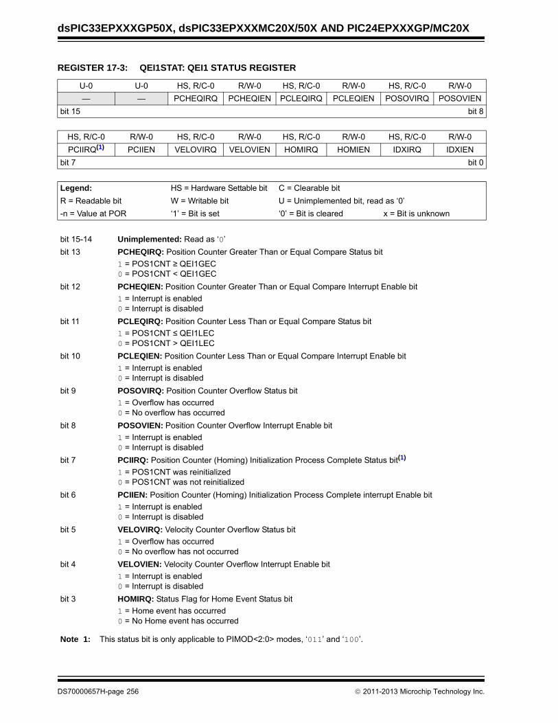
dsPIC33EPXXXGP50X, dsPIC33EPXXXMC20X/50X AND PIC24EPXXXGP/MC20X
REGISTER 17-3: QEI1STAT: QEI1 STATUS REGISTER
U-0 U-0 HS, R/C-0 R/W-0 HS, R/C-0 R/W-0 HS, R/C-0 R/W-0
— — PCHEQIRQ PCHEQIEN PCLEQIRQ PCLEQIEN POSOVIRQ POSOVIEN
bit 15 bit 8
HS, R/C-0 R/W-0 HS, R/C-0 R/W-0 HS, R/C-0 R/W-0 HS, R/C-0 R/W-0
PCIIRQ(1) PCIIEN VELOVIRQ VELOVIEN HOMIRQ HOMIEN IDXIRQ IDXIEN
bit 7 bit 0
Legend: HS = Hardware Settable bit C = Clearable bit
R = Readable bit W = Writable bit U = Unimplemented bit, read as ‘0’
-n = Value at POR ‘1’ = Bit is set ‘0’ = Bit is cleared x = Bit is unknown
bit 15-14 Unimplemented: Read as ‘0’
bit 13 PCHEQIRQ: Position Counter Greater Than or Equal Compare Status bit
1 = POS1CNT ≥ QEI1GEC0 = POS1CNT < QEI1GEC
bit 12 PCHEQIEN: Position Counter Greater Than or Equal Compare Interrupt Enable bit
1 = Interrupt is enabled0 = Interrupt is disabled
bit 11 PCLEQIRQ: Position Counter Less Than or Equal Compare Status bit
1 = POS1CNT ≤ QEI1LEC0 = POS1CNT > QEI1LEC
bit 10 PCLEQIEN: Position Counter Less Than or Equal Compare Interrupt Enable bit
1 = Interrupt is enabled0 = Interrupt is disabled
bit 9 POSOVIRQ: Position Counter Overflow Status bit
1 = Overflow has occurred0 = No overflow has occurred
bit 8 POSOVIEN: Position Counter Overflow Interrupt Enable bit
1 = Interrupt is enabled0 = Interrupt is disabled
bit 7 PCIIRQ: Position Counter (Homing) Initialization Process Complete Status bit(1)
1 = POS1CNT was reinitialized0 = POS1CNT was not reinitialized
bit 6 PCIIEN: Position Counter (Homing) Initialization Process Complete interrupt Enable bit
1 = Interrupt is enabled0 = Interrupt is disabled
bit 5 VELOVIRQ: Velocity Counter Overflow Status bit
1 = Overflow has occurred0 = No overflow has not occurred
bit 4 VELOVIEN: Velocity Counter Overflow Interrupt Enable bit
1 = Interrupt is enabled0 = Interrupt is disabled
bit 3 HOMIRQ: Status Flag for Home Event Status bit
1 = Home event has occurred0 = No Home event has occurred
Note 1: This status bit is only applicable to PIMOD<2:0> modes, ‘011’ and ‘100’.
DS70000657H-page 256 2011-2013 Microchip Technology Inc.

dsPIC33EPXXXGP50X, dsPIC33EPXXXMC20X/50X AND PIC24EPXXXGP/MC20X
bit 2 HOMIEN: Home Input Event Interrupt Enable bit
1 = Interrupt is enabled0 = Interrupt is disabled
bit 1 IDXIRQ: Status Flag for Index Event Status bit
1 = Index event has occurred0 = No Index event has occurred
bit 0 IDXIEN: Index Input Event Interrupt Enable bit
1 = Interrupt is enabled0 = Interrupt is disabled
REGISTER 17-3: QEI1STAT: QEI1 STATUS REGISTER (CONTINUED)
Note 1: This status bit is only applicable to PIMOD<2:0> modes, ‘011’ and ‘100’.
2011-2013 Microchip Technology Inc. DS70000657H-page 257
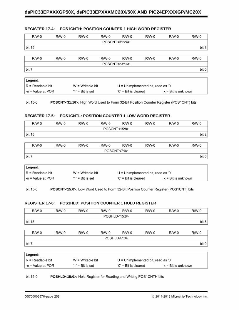
dsPIC33EPXXXGP50X, dsPIC33EPXXXMC20X/50X AND PIC24EPXXXGP/MC20X
REGISTER 17-4: POS1CNTH: POSITION COUNTER 1 HIGH WORD REGISTER
R/W-0 R/W-0 R/W-0 R/W-0 R/W-0 R/W-0 R/W-0 R/W-0
POSCNT<31:24>
bit 15 bit 8
R/W-0 R/W-0 R/W-0 R/W-0 R/W-0 R/W-0 R/W-0 R/W-0
POSCNT<23:16>
bit 7 bit 0
Legend:
R = Readable bit W = Writable bit U = Unimplemented bit, read as ‘0’
-n = Value at POR ‘1’ = Bit is set ‘0’ = Bit is cleared x = Bit is unknown
bit 15-0 POSCNT<31:16>: High Word Used to Form 32-Bit Position Counter Register (POS1CNT) bits
REGISTER 17-5: POS1CNTL: POSITION COUNTER 1 LOW WORD REGISTER
R/W-0 R/W-0 R/W-0 R/W-0 R/W-0 R/W-0 R/W-0 R/W-0
POSCNT<15:8>
bit 15 bit 8
R/W-0 R/W-0 R/W-0 R/W-0 R/W-0 R/W-0 R/W-0 R/W-0
POSCNT<7:0>
bit 7 bit 0
Legend:
R = Readable bit W = Writable bit U = Unimplemented bit, read as ‘0’
-n = Value at POR ‘1’ = Bit is set ‘0’ = Bit is cleared x = Bit is unknown
bit 15-0 POSCNT<15:0>: Low Word Used to Form 32-Bit Position Counter Register (POS1CNT) bits
REGISTER 17-6: POS1HLD: POSITION COUNTER 1 HOLD REGISTER
R/W-0 R/W-0 R/W-0 R/W-0 R/W-0 R/W-0 R/W-0 R/W-0
POSHLD<15:8>
bit 15 bit 8
R/W-0 R/W-0 R/W-0 R/W-0 R/W-0 R/W-0 R/W-0 R/W-0
POSHLD<7:0>
bit 7 bit 0
Legend:
R = Readable bit W = Writable bit U = Unimplemented bit, read as ‘0’
-n = Value at POR ‘1’ = Bit is set ‘0’ = Bit is cleared x = Bit is unknown
bit 15-0 POSHLD<15:0>: Hold Register for Reading and Writing POS1CNTH bits
DS70000657H-page 258 2011-2013 Microchip Technology Inc.

dsPIC33EPXXXGP50X, dsPIC33EPXXXMC20X/50X AND PIC24EPXXXGP/MC20X
REGISTER 17-7: VEL1CNT: VELOCITY COUNTER 1 REGISTER
R/W-0 R/W-0 R/W-0 R/W-0 R/W-0 R/W-0 R/W-0 R/W-0
VELCNT<15:8>
bit 15 bit 8
R/W-0 R/W-0 R/W-0 R/W-0 R/W-0 R/W-0 R/W-0 R/W-0
VELCNT<7:0>
bit 7 bit 0
Legend:
R = Readable bit W = Writable bit U = Unimplemented bit, read as ‘0’
-n = Value at POR ‘1’ = Bit is set ‘0’ = Bit is cleared x = Bit is unknown
bit 15-0 VELCNT<15:0>: Velocity Counter bits
REGISTER 17-8: INDX1CNTH: INDEX COUNTER 1 HIGH WORD REGISTER
R/W-0 R/W-0 R/W-0 R/W-0 R/W-0 R/W-0 R/W-0 R/W-0
INDXCNT<31:24>
bit 15 bit 8
R/W-0 R/W-0 R/W-0 R/W-0 R/W-0 R/W-0 R/W-0 R/W-0
INDXCNT<23:16>
bit 7 bit 0
Legend:
R = Readable bit W = Writable bit U = Unimplemented bit, read as ‘0’
-n = Value at POR ‘1’ = Bit is set ‘0’ = Bit is cleared x = Bit is unknown
bit 15-0 INDXCNT<31:16>: High Word Used to Form 32-Bit Index Counter Register (INDX1CNT) bits
REGISTER 17-9: INDX1CNTL: INDEX COUNTER 1 LOW WORD REGISTER
R/W-0 R/W-0 R/W-0 R/W-0 R/W-0 R/W-0 R/W-0 R/W-0
INDXCNT<15:8>
bit 15 bit 8
R/W-0 R/W-0 R/W-0 R/W-0 R/W-0 R/W-0 R/W-0 R/W-0
INDXCNT<7:0>
bit 7 bit 0
Legend:
R = Readable bit W = Writable bit U = Unimplemented bit, read as ‘0’
-n = Value at POR ‘1’ = Bit is set ‘0’ = Bit is cleared x = Bit is unknown
bit 15-0 INDXCNT<15:0>: Low Word Used to Form 32-Bit Index Counter Register (INDX1CNT) bits
2011-2013 Microchip Technology Inc. DS70000657H-page 259

dsPIC33EPXXXGP50X, dsPIC33EPXXXMC20X/50X AND PIC24EPXXXGP/MC20X
REGISTER 17-10: INDX1HLD: INDEX COUNTER 1 HOLD REGISTER
R/W-0 R/W-0 R/W-0 R/W-0 R/W-0 R/W-0 R/W-0 R/W-0
INDXHLD<15:8>
bit 15 bit 8
R/W-0 R/W-0 R/W-0 R/W-0 R/W-0 R/W-0 R/W-0 R/W-0
INDXHLD<7:0>
bit 7 bit 0
Legend:
R = Readable bit W = Writable bit U = Unimplemented bit, read as ‘0’
-n = Value at POR ‘1’ = Bit is set ‘0’ = Bit is cleared x = Bit is unknown
bit 15-0 INDXHLD<15:0>: Hold Register for Reading and Writing INDX1CNTH bits
REGISTER 17-11: QEI1ICH: QEI1 INITIALIZATION/CAPTURE HIGH WORD REGISTER
R/W-0 R/W-0 R/W-0 R/W-0 R/W-0 R/W-0 R/W-0 R/W-0
QEIIC<31:24>
bit 15 bit 8
R/W-0 R/W-0 R/W-0 R/W-0 R/W-0 R/W-0 R/W-0 R/W-0
QEIIC<23:16>
bit 7 bit 0
Legend:
R = Readable bit W = Writable bit U = Unimplemented bit, read as ‘0’
-n = Value at POR ‘1’ = Bit is set ‘0’ = Bit is cleared x = Bit is unknown
bit 15-0 QEIIC<31:16>: High Word Used to Form 32-Bit Initialization/Capture Register (QEI1IC) bits
REGISTER 17-12: QEI1ICL: QEI1 INITIALIZATION/CAPTURE LOW WORD REGISTER
R/W-0 R/W-0 R/W-0 R/W-0 R/W-0 R/W-0 R/W-0 R/W-0
QEIIC<15:8>
bit 15 bit 8
R/W-0 R/W-0 R/W-0 R/W-0 R/W-0 R/W-0 R/W-0 R/W-0
QEIIC<7:0>
bit 7 bit 0
Legend:
R = Readable bit W = Writable bit U = Unimplemented bit, read as ‘0’
-n = Value at POR ‘1’ = Bit is set ‘0’ = Bit is cleared x = Bit is unknown
bit 15-0 QEIIC<15:0>: Low Word Used to Form 32-Bit Initialization/Capture Register (QEI1IC) bits
DS70000657H-page 260 2011-2013 Microchip Technology Inc.

dsPIC33EPXXXGP50X, dsPIC33EPXXXMC20X/50X AND PIC24EPXXXGP/MC20X
REGISTER 17-13: QEI1LECH: QEI1 LESS THAN OR EQUAL COMPARE HIGH WORD REGISTER
R/W-0 R/W-0 R/W-0 R/W-0 R/W-0 R/W-0 R/W-0 R/W-0
QEILEC<31:24>
bit 15 bit 8
R/W-0 R/W-0 R/W-0 R/W-0 R/W-0 R/W-0 R/W-0 R/W-0
QEILEC<23:16>
bit 7 bit 0
Legend:
R = Readable bit W = Writable bit U = Unimplemented bit, read as ‘0’
-n = Value at POR ‘1’ = Bit is set ‘0’ = Bit is cleared x = Bit is unknown
bit 15-0 QEILEC<31:16>: High Word Used to Form 32-Bit Less Than or Equal Compare Register (QEI1LEC) bits
REGISTER 17-14: QEI1LECL: QEI1 LESS THAN OR EQUAL COMPARE LOW WORD REGISTER
R/W-0 R/W-0 R/W-0 R/W-0 R/W-0 R/W-0 R/W-0 R/W-0
QEILEC<15:8>
bit 15 bit 8
R/W-0 R/W-0 R/W-0 R/W-0 R/W-0 R/W-0 R/W-0 R/W-0
QEILEC<7:0>
bit 7 bit 0
Legend:
R = Readable bit W = Writable bit U = Unimplemented bit, read as ‘0’
-n = Value at POR ‘1’ = Bit is set ‘0’ = Bit is cleared x = Bit is unknown
bit 15-0 QEILEC<15:0>: Low Word Used to Form 32-Bit Less Than or Equal Compare Register (QEI1LEC) bits
2011-2013 Microchip Technology Inc. DS70000657H-page 261

dsPIC33EPXXXGP50X, dsPIC33EPXXXMC20X/50X AND PIC24EPXXXGP/MC20X
REGISTER 17-15: QEI1GECH: QEI1 GREATER THAN OR EQUAL COMPARE HIGH WORD REGISTER
R/W-0 R/W-0 R/W-0 R/W-0 R/W-0 R/W-0 R/W-0 R/W-0
QEIGEC<31:24>
bit 15 bit 8
R/W-0 R/W-0 R/W-0 R/W-0 R/W-0 R/W-0 R/W-0 R/W-0
QEIGEC<23:16>
bit 7 bit 0
Legend:
R = Readable bit W = Writable bit U = Unimplemented bit, read as ‘0’
-n = Value at POR ‘1’ = Bit is set ‘0’ = Bit is cleared x = Bit is unknown
bit 15-0 QEIGEC<31:16>: High Word Used to Form 32-Bit Greater Than or Equal Compare Register (QEI1GEC) bits
REGISTER 17-16: QEI1GECL: QEI1 GREATER THAN OR EQUAL COMPARE LOW WORD REGISTER
R/W-0 R/W-0 R/W-0 R/W-0 R/W-0 R/W-0 R/W-0 R/W-0
QEIGEC<15:8>
bit 15 bit 8
R/W-0 R/W-0 R/W-0 R/W-0 R/W-0 R/W-0 R/W-0 R/W-0
QEIGEC<7:0>
bit 7 bit 0
Legend:
R = Readable bit W = Writable bit U = Unimplemented bit, read as ‘0’
-n = Value at POR ‘1’ = Bit is set ‘0’ = Bit is cleared x = Bit is unknown
bit 15-0 QEIGEC<15:0>: Low Word Used to Form 32-Bit Greater Than or Equal Compare Register (QEI1GEC) bits
DS70000657H-page 262 2011-2013 Microchip Technology Inc.

dsPIC33EPXXXGP50X, dsPIC33EPXXXMC20X/50X AND PIC24EPXXXGP/MC20X
REGISTER 17-17: INT1TMRH: INTERVAL 1 TIMER HIGH WORD REGISTER
R/W-0 R/W-0 R/W-0 R/W-0 R/W-0 R/W-0 R/W-0 R/W-0
INTTMR<31:24>
bit 15 bit 8
R/W-0 R/W-0 R/W-0 R/W-0 R/W-0 R/W-0 R/W-0 R/W-0
INTTMR<23:16>
bit 7 bit 0
Legend:
R = Readable bit W = Writable bit U = Unimplemented bit, read as ‘0’
-n = Value at POR ‘1’ = Bit is set ‘0’ = Bit is cleared x = Bit is unknown
bit 15-0 INTTMR<31:16>: High Word Used to Form 32-Bit Interval Timer Register (INT1TMR) bits
REGISTER 17-18: INT1TMRL: INTERVAL 1 TIMER LOW WORD REGISTER
R/W-0 R/W-0 R/W-0 R/W-0 R/W-0 R/W-0 R/W-0 R/W-0
INTTMR<15:8>
bit 15 bit 8
R/W-0 R/W-0 R/W-0 R/W-0 R/W-0 R/W-0 R/W-0 R/W-0
INTTMR<7:0>
bit 7 bit 0
Legend:
R = Readable bit W = Writable bit U = Unimplemented bit, read as ‘0’
-n = Value at POR ‘1’ = Bit is set ‘0’ = Bit is cleared x = Bit is unknown
bit 15-0 INTTMR<15:0>: Low Word Used to Form 32-Bit Interval Timer Register (INT1TMR) bits
2011-2013 Microchip Technology Inc. DS70000657H-page 263

dsPIC33EPXXXGP50X, dsPIC33EPXXXMC20X/50X AND PIC24EPXXXGP/MC20X
REGISTER 17-19: INT1HLDH: INTERVAL 1 TIMER HOLD HIGH WORD REGISTER
R/W-0 R/W-0 R/W-0 R/W-0 R/W-0 R/W-0 R/W-0 R/W-0
INTHLD<31:24>
bit 15 bit 8
R/W-0 R/W-0 R/W-0 R/W-0 R/W-0 R/W-0 R/W-0 R/W-0
INTHLD<23:16>
bit 7 bit 0
Legend:
R = Readable bit W = Writable bit U = Unimplemented bit, read as ‘0’
-n = Value at POR ‘1’ = Bit is set ‘0’ = Bit is cleared x = Bit is unknown
bit 15-0 INTHLD<31:16>: Hold Register for Reading and Writing INT1TMRH bits
REGISTER 17-20: INT1HLDL: INTERVAL 1 TIMER HOLD LOW WORD REGISTER
R/W-0 R/W-0 R/W-0 R/W-0 R/W-0 R/W-0 R/W-0 R/W-0
INTHLD<15:8>
bit 15 bit 8
R/W-0 R/W-0 R/W-0 R/W-0 R/W-0 R/W-0 R/W-0 R/W-0
INTHLD<7:0>
bit 7 bit 0
Legend:
R = Readable bit W = Writable bit U = Unimplemented bit, read as ‘0’
-n = Value at POR ‘1’ = Bit is set ‘0’ = Bit is cleared x = Bit is unknown
bit 15-0 INTHLD<15:0>: Hold Register for Reading and Writing INT1TMRL bits
DS70000657H-page 264 2011-2013 Microchip Technology Inc.
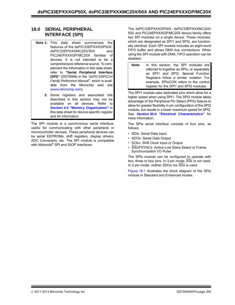
dsPIC33EPXXXGP50X, dsPIC33EPXXXMC20X/50X AND PIC24EPXXXGP/MC20X
18.0 SERIAL PERIPHERAL INTERFACE (SPI)
The SPI module is a synchronous serial interface,useful for communicating with other peripheral ormicrocontroller devices. These peripheral devices canbe serial EEPROMs, shift registers, display drivers,ADC Converters, etc. The SPI module is compatiblewith Motorola® SPI and SIOP interfaces.
The dsPIC33EPXXXGP50X, dsPIC33EPXXXMC20X/50X and PIC24EPXXXGP/MC20X device family offerstwo SPI modules on a single device. These modules,which are designated as SPI1 and SPI2, are function-ally identical. Each SPI module includes an eight-wordFIFO buffer and allows DMA bus connections. Whenusing the SPI module with DMA, FIFO operation can bedisabled.
The SPI1 module uses dedicated pins which allow for ahigher speed when using SPI1. The SPI2 module takesadvantage of the Peripheral Pin Select (PPS) feature toallow for greater flexibility in pin configuration of the SPI2module, but results in a lower maximum speed for SPI2.See Section 30.0 “Electrical Characteristics” formore information.
The SPIx serial interface consists of four pins, asfollows:
• SDIx: Serial Data Input• SDOx: Serial Data Output• SCKx: Shift Clock Input or Output• SSx/FSYNCx: Active-Low Slave Select or Frame
Synchronization I/O Pulse
The SPIx module can be configured to operate withtwo, three or four pins. In 3-pin mode, SSx is not used.In 2-pin mode, neither SDOx nor SSx is used.
Figure 18-1 illustrates the block diagram of the SPIxmodule in Standard and Enhanced modes.
Note 1: This data sheet summarizes thefeatures of the dsPIC33EPXXXGP50X,dsPIC33EPXXXMC20X/50X andPIC24EPXXXGP/MC20X families ofdevices. It is not intended to be acomprehensive reference source. To com-plement the information in this data sheet,refer to “Serial Peripheral Interface(SPI)” (DS70569) in the “dsPIC33/PIC24Family Reference Manual”, which is avail-able from the Microchip web site(www.microchip.com).
2: Some registers and associated bitsdescribed in this section may not beavailable on all devices. Refer toSection 4.0 “Memory Organization” inthis data sheet for device-specific registerand bit information.
Note: In this section, the SPI modules arereferred to together as SPIx, or separatelyas SPI1 and SPI2. Special FunctionRegisters follow a similar notation. Forexample, SPIxCON refers to the controlregister for the SPI1 and SPI2 modules.
2011-2013 Microchip Technology Inc. DS70000657H-page 265

dsPIC33EPXXXGP50X, dsPIC33EPXXXMC20X/50X AND PIC24EPXXXGP/MC20X
FIGURE 18-1: SPIx MODULE BLOCK DIAGRAM
Internal Data Bus
SDIx
SDOx
SSx/FSYNCx
SCKx
bit 0
Shift Control
EdgeSelect
FPPrimary1:1/4/16/64
Enable
Prescaler
SyncControl
TransferTransfer
Write SPIxBUFRead SPIxBUF
16
SPIxCON1<1:0>
SPIxCON1<4:2>
Master Clock
Note 1: In Standard mode, the FIFO is only one level deep.
ClockControl
SecondaryPrescaler
1:1 to 1:8
SPIxSR
8-Level FIFOReceive Buffer(1)
8-Level FIFOTransmit Buffer(1)
SPIxBUF
DS70000657H-page 266 2011-2013 Microchip Technology Inc.

dsPIC33EPXXXGP50X, dsPIC33EPXXXMC20X/50X AND PIC24EPXXXGP/MC20X
18.1 SPI Helpful Tips
1. In Frame mode, if there is a possibility that themaster may not be initialized before the slave:
a) If FRMPOL (SPIxCON2<13>) = 1, use apull-down resistor on SSx.
b) If FRMPOL = 0, use a pull-up resistor onSSx.
2. In Non-Framed 3-Wire mode, (i.e., not usingSSx from a master):
a) If CKP (SPIxCON1<6>) = 1, always place apull-up resistor on SSx.
b) If CKP = 0, always place a pull-downresistor on SSx.
3. FRMEN (SPIxCON2<15>) = 1 and SSEN(SPIxCON1<7>) = 1 are exclusive and invalid.In Frame mode, SCKx is continuous and theFrame Sync pulse is active on the SSx pin,which indicates the start of a data frame.
4. In Master mode only, set the SMP bit(SPIxCON1<9>) to a ‘1’ for the fastest SPIx datarate possible. The SMP bit can only be set at thesame time or after the MSTEN bit(SPIxCON1<5>) is set.
To avoid invalid slave read data to the master, theuser’s master software must ensure enough time forslave software to fill its write buffer before the userapplication initiates a master write/read cycle. It isalways advisable to preload the SPIxBUF Transmitregister in advance of the next master transactioncycle. SPIxBUF is transferred to the SPIx Shift registerand is empty once the data transmission begins.
18.2 SPI Resources
Many useful resources are provided on the main prod-uct page of the Microchip web site for the devices listedin this data sheet. This product page, which can beaccessed using this link, contains the latest updatesand additional information.
18.2.1 KEY RESOURCES
• “Serial Peripheral Interface (SPI)” (DS70569) in the “dsPIC33/PIC24 Family Reference Manual”
• Code Samples
• Application Notes
• Software Libraries
• Webinars
• All Related “dsPIC33/PIC24 Family Reference Manual” Sections
• Development Tools
Note: This insures that the first frametransmission after initialization is notshifted or corrupted.
Note: This will insure that during power-up andinitialization the master/slave will not loseSync due to an errant SCKx transition thatwould cause the slave to accumulate datashift errors for both transmit and receiveappearing as corrupted data.
Note: Not all third-party devices support Framemode timing. Refer to the SPIxspecifications in Section 30.0 “ElectricalCharacteristics” for details.
Note: In the event you are not able to access theproduct page using the link above, enterthis URL in your browser:http://www.microchip.com/wwwproducts/Devices.aspx?dDocName=en555464
2011-2013 Microchip Technology Inc. DS70000657H-page 267

dsPIC33EPXXXGP50X, dsPIC33EPXXXMC20X/50X AND PIC24EPXXXGP/MC20X
18.3 SPIx Control Registers
REGISTER 18-1: SPIxSTAT: SPIx STATUS AND CONTROL REGISTER
R/W-0 U-0 R/W-0 U-0 U-0 R/W-0 R/W-0 R/W-0
SPIEN — SPISIDL — — SPIBEC<2:0>
bit 15 bit 8
R/W-0 R/C-0, HS R/W-0 R/W-0 R/W-0 R/W-0 R-0, HS, HC R-0, HS, HC
SRMPT SPIROV SRXMPT SISEL2 SISEL1 SISEL0 SPITBF SPIRBF
bit 7 bit 0
Legend: C = Clearable bit HS = Hardware Settable bit HC = Hardware Clearable bit
R = Readable bit W = Writable bit U = Unimplemented bit, read as ‘0’
-n = Value at POR ‘1’ = Bit is set ‘0’ = Bit is cleared x = Bit is unknown
bit 15 SPIEN: SPIx Enable bit
1 = Enables the module and configures SCKx, SDOx, SDIx and SSx as serial port pins0 = Disables the module
bit 14 Unimplemented: Read as ‘0’
bit 13 SPISIDL: SPIx Stop in Idle Mode bit
1 = Discontinues the module operation when device enters Idle mode0 = Continues the module operation in Idle mode
bit 12-11 Unimplemented: Read as ‘0’
bit 10-8 SPIBEC<2:0>: SPIx Buffer Element Count bits (valid in Enhanced Buffer mode)
Master mode:Number of SPIx transfers that are pending.
Slave mode:Number of SPIx transfers that are unread.
bit 7 SRMPT: SPIx Shift Register (SPIxSR) Empty bit (valid in Enhanced Buffer mode)
1 = SPIx Shift register is empty and Ready-To-Send or receive the data0 = SPIx Shift register is not empty
bit 6 SPIROV: SPIx Receive Overflow Flag bit
1 = A new byte/word is completely received and discarded; the user application has not read the previousdata in the SPIxBUF register
0 = No overflow has occurred
bit 5 SRXMPT: SPIx Receive FIFO Empty bit (valid in Enhanced Buffer mode)
1 = RX FIFO is empty0 = RX FIFO is not empty
bit 4-2 SISEL<2:0>: SPIx Buffer Interrupt Mode bits (valid in Enhanced Buffer mode)
111 = Interrupt when the SPIx transmit buffer is full (SPITBF bit is set)110 = Interrupt when last bit is shifted into SPIxSR and as a result, the TX FIFO is empty101 = Interrupt when the last bit is shifted out of SPIxSR and the transmit is complete100 = Interrupt when one data is shifted into the SPIxSR and as a result, the TX FIFO has one open
memory location011 = Interrupt when the SPIx receive buffer is full (SPIRBF bit is set)010 = Interrupt when the SPIx receive buffer is 3/4 or more full001 = Interrupt when data is available in the receive buffer (SRMPT bit is set)000 = Interrupt when the last data in the receive buffer is read and as a result, the buffer is empty
(SRXMPT bit is set)
DS70000657H-page 268 2011-2013 Microchip Technology Inc.

dsPIC33EPXXXGP50X, dsPIC33EPXXXMC20X/50X AND PIC24EPXXXGP/MC20X
bit 1 SPITBF: SPIx Transmit Buffer Full Status bit
1 = Transmit not yet started, SPIxTXB is full0 = Transmit started, SPIxTXB is empty
Standard Buffer mode:Automatically set in hardware when core writes to the SPIxBUF location, loading SPIxTXB.Automatically cleared in hardware when SPIx module transfers data from SPIxTXB to SPIxSR.
Enhanced Buffer mode:Automatically set in hardware when the CPU writes to the SPIxBUF location, loading the last availablebuffer location. Automatically cleared in hardware when a buffer location is available for a CPU writeoperation.
bit 0 SPIRBF: SPIx Receive Buffer Full Status bit
1 = Receive is complete, SPIxRXB is full0 = Receive is incomplete, SPIxRXB is empty
Standard Buffer mode:Automatically set in hardware when SPIx transfers data from SPIxSR to SPIxRXB. Automaticallycleared in hardware when the core reads the SPIxBUF location, reading SPIxRXB.
Enhanced Buffer mode:Automatically set in hardware when SPIx transfers data from SPIxSR to the buffer, filling the last unreadbuffer location. Automatically cleared in hardware when a buffer location is available for a transfer fromSPIxSR.
REGISTER 18-1: SPIxSTAT: SPIx STATUS AND CONTROL REGISTER (CONTINUED)
2011-2013 Microchip Technology Inc. DS70000657H-page 269

dsPIC33EPXXXGP50X, dsPIC33EPXXXMC20X/50X AND PIC24EPXXXGP/MC20X
REGISTER 18-2: SPIXCON1: SPIX CONTROL REGISTER 1
U-0 U-0 U-0 R/W-0 R/W-0 R/W-0 R/W-0 R/W-0
— — — DISSCK DISSDO MODE16 SMP CKE(1)
bit 15 bit 8
R/W-0 R/W-0 R/W-0 R/W-0 R/W-0 R/W-0 R/W-0 R/W-0
SSEN(2) CKP MSTEN SPRE2(3) SPRE1(3) SPRE0(3) PPRE1(3) PPRE0(3)
bit 7 bit 0
Legend:
R = Readable bit W = Writable bit U = Unimplemented bit, read as ‘0’
-n = Value at POR ‘1’ = Bit is set ‘0’ = Bit is cleared x = Bit is unknown
bit 15-13 Unimplemented: Read as ‘0’
bit 12 DISSCK: Disable SCKx Pin bit (SPIx Master modes only)
1 = Internal SPIx clock is disabled, pin functions as I/O0 = Internal SPIx clock is enabled
bit 11 DISSDO: Disable SDOx Pin bit
1 = SDOx pin is not used by the module; pin functions as I/O0 = SDOx pin is controlled by the module
bit 10 MODE16: Word/Byte Communication Select bit
1 = Communication is word-wide (16 bits)0 = Communication is byte-wide (8 bits)
bit 9 SMP: SPIx Data Input Sample Phase bit
Master mode:1 = Input data is sampled at end of data output time0 = Input data is sampled at middle of data output time
Slave mode:SMP must be cleared when SPIx is used in Slave mode.
bit 8 CKE: SPIx Clock Edge Select bit(1)
1 = Serial output data changes on transition from active clock state to Idle clock state (refer to bit 6)0 = Serial output data changes on transition from Idle clock state to active clock state (refer to bit 6)
bit 7 SSEN: Slave Select Enable bit (Slave mode)(2)
1 = SSx pin is used for Slave mode0 = SSx pin is not used by the module; pin is controlled by port function
bit 6 CKP: Clock Polarity Select bit
1 = Idle state for clock is a high level; active state is a low level0 = Idle state for clock is a low level; active state is a high level
bit 5 MSTEN: Master Mode Enable bit
1 = Master mode0 = Slave mode
Note 1: The CKE bit is not used in Framed SPI modes. Program this bit to ‘0’ for Framed SPI modes (FRMEN = 1).
2: This bit must be cleared when FRMEN = 1.
3: Do not set both primary and secondary prescalers to the value of 1:1.
DS70000657H-page 270 2011-2013 Microchip Technology Inc.
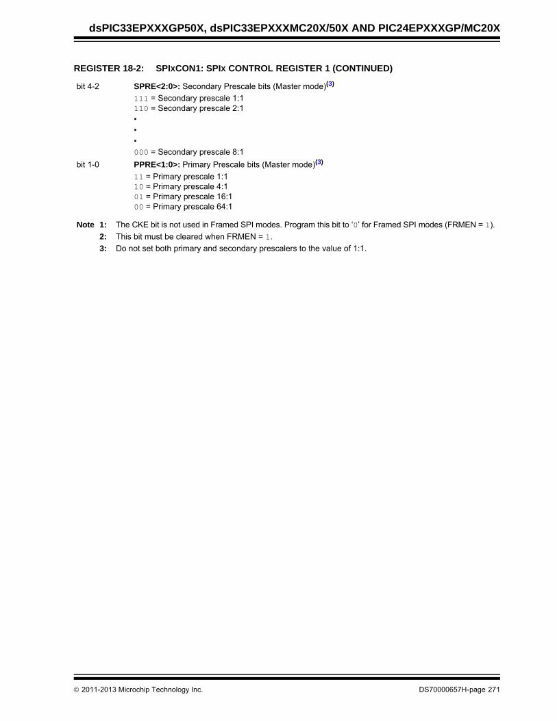
dsPIC33EPXXXGP50X, dsPIC33EPXXXMC20X/50X AND PIC24EPXXXGP/MC20X
bit 4-2 SPRE<2:0>: Secondary Prescale bits (Master mode)(3)
111 = Secondary prescale 1:1110 = Secondary prescale 2:1•••000 = Secondary prescale 8:1
bit 1-0 PPRE<1:0>: Primary Prescale bits (Master mode)(3)
11 = Primary prescale 1:110 = Primary prescale 4:101 = Primary prescale 16:100 = Primary prescale 64:1
REGISTER 18-2: SPIXCON1: SPIX CONTROL REGISTER 1 (CONTINUED)
Note 1: The CKE bit is not used in Framed SPI modes. Program this bit to ‘0’ for Framed SPI modes (FRMEN = 1).
2: This bit must be cleared when FRMEN = 1.
3: Do not set both primary and secondary prescalers to the value of 1:1.
2011-2013 Microchip Technology Inc. DS70000657H-page 271
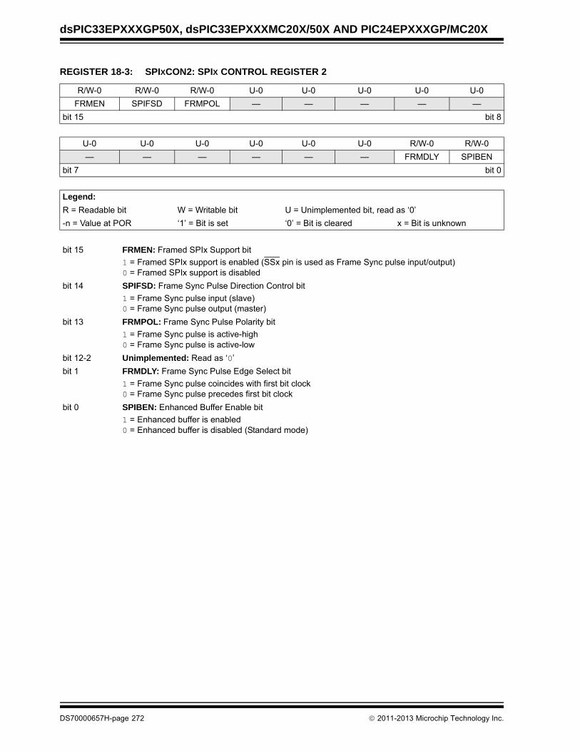
dsPIC33EPXXXGP50X, dsPIC33EPXXXMC20X/50X AND PIC24EPXXXGP/MC20X
REGISTER 18-3: SPIXCON2: SPIX CONTROL REGISTER 2
R/W-0 R/W-0 R/W-0 U-0 U-0 U-0 U-0 U-0
FRMEN SPIFSD FRMPOL — — — — —
bit 15 bit 8
U-0 U-0 U-0 U-0 U-0 U-0 R/W-0 R/W-0
— — — — — — FRMDLY SPIBEN
bit 7 bit 0
Legend:
R = Readable bit W = Writable bit U = Unimplemented bit, read as ‘0’
-n = Value at POR ‘1’ = Bit is set ‘0’ = Bit is cleared x = Bit is unknown
bit 15 FRMEN: Framed SPIx Support bit
1 = Framed SPIx support is enabled (SSx pin is used as Frame Sync pulse input/output)0 = Framed SPIx support is disabled
bit 14 SPIFSD: Frame Sync Pulse Direction Control bit
1 = Frame Sync pulse input (slave)0 = Frame Sync pulse output (master)
bit 13 FRMPOL: Frame Sync Pulse Polarity bit
1 = Frame Sync pulse is active-high0 = Frame Sync pulse is active-low
bit 12-2 Unimplemented: Read as ‘0’
bit 1 FRMDLY: Frame Sync Pulse Edge Select bit
1 = Frame Sync pulse coincides with first bit clock0 = Frame Sync pulse precedes first bit clock
bit 0 SPIBEN: Enhanced Buffer Enable bit
1 = Enhanced buffer is enabled0 = Enhanced buffer is disabled (Standard mode)
DS70000657H-page 272 2011-2013 Microchip Technology Inc.

dsPIC33EPXXXGP50X, dsPIC33EPXXXMC20X/50X AND PIC24EPXXXGP/MC20X
19.0 INTER-INTEGRATED CIRCUIT™ (I2C™)
The dsPIC33EPXXXGP50X, dsPIC33EPXXXMC20X/50X and PIC24EPXXXGP/MC20X family of devicescontains two Inter-Integrated Circuit (I2C) modules:I2C1 and I2C2.
The I2C module provides complete hardware supportfor both Slave and Multi-Master modes of the I2C serialcommunication standard, with a 16-bit interface.
The I2C module has a 2-pin interface:
• The SCLx pin is clock• The SDAx pin is data
The I2C module offers the following key features:
• I2C interface supporting both Master and Slave modes of operation
• I2C Slave mode supports 7 and 10-bit addressing
• I2C Master mode supports 7 and 10-bit addressing
• I2C port allows bidirectional transfers between master and slaves
• Serial clock synchronization for I2C port can be used as a handshake mechanism to suspend and resume serial transfer (SCLREL control)
• I2C supports multi-master operation, detects bus collision and arbitrates accordingly
• Intelligent Platform Management Interface (IPMI) support
• System Management Bus (SMBus) support
Note 1: This data sheet summarizes thefeatures of the dsPIC33EPXXXGP50X,dsPIC33EPXXXMC20X/50X andPIC24EPXXXGP/MC20X families ofdevices. It is not intended to be acomprehensive reference source. To com-plement the information in this data sheet,refer to “Inter-Integrated Circuit™(I2C™)” (DS70330) in the “dsPIC33/PIC24 Family Reference Manual”, whichis available from the Microchip web site(www.microchip.com).
2: Some registers and associated bitsdescribed in this section may not beavailable on all devices. Refer toSection 4.0 “Memory Organization” inthis data sheet for device-specific registerand bit information.
3: There are minimum bit rates of approxi-mately FCY/512. As a result, highprocessor speeds may not support100 Kbit/second operation. See timingspecifications, IM10 and IM11, and the“Baud Rate Generator” in the “dsPIC33/PIC24 Family Reference Manual”.
2011-2013 Microchip Technology Inc. DS70000657H-page 273

dsPIC33EPXXXGP50X, dsPIC33EPXXXMC20X/50X AND PIC24EPXXXGP/MC20X
FIGURE 19-1: I2Cx BLOCK DIAGRAM (X = 1 OR 2)
InternalData Bus
SCLx/ASCLx
SDAx/ASDAx
Shift
Match Detect
Start and StopBit Detect
Clock
Address Match
ClockStretching
I2CxTRN
LSbShift Clock
BRG Down Counter
ReloadControl
FP/2
Start and StopBit Generation
AcknowledgeGeneration
CollisionDetect
I2CxCON
I2CxSTAT
Co
ntr
ol L
og
ic
Read
LSb
Write
Read
I2CxBRG
I2CxRSR
Write
Read
Write
Read
Write
Read
Write
Read
Write
Read
I2CxMSK
I2CxRCV
I2CxADD
DS70000657H-page 274 2011-2013 Microchip Technology Inc.

dsPIC33EPXXXGP50X, dsPIC33EPXXXMC20X/50X AND PIC24EPXXXGP/MC20X
19.1 I2C Resources
Many useful resources are provided on the main prod-uct page of the Microchip web site for the devices listedin this data sheet. This product page, which can beaccessed using this link, contains the latest updatesand additional information.
19.1.1 KEY RESOURCES
• “Inter-Integrated Circuit (I2C)” (DS70330) in the “dsPIC33/PIC24 Family Reference Manual”
• Code Samples
• Application Notes
• Software Libraries
• Webinars
• All Related “dsPIC33/PIC24 Family Reference Manual” Sections
• Development Tools
Note: In the event you are not able to access theproduct page using the link above, enterthis URL in your browser:http://www.microchip.com/wwwproducts/Devices.aspx?dDocName=en555464
2011-2013 Microchip Technology Inc. DS70000657H-page 275

dsPIC33EPXXXGP50X, dsPIC33EPXXXMC20X/50X AND PIC24EPXXXGP/MC20X
19.2 I2C Control Registers
REGISTER 19-1: I2CxCON: I2Cx CONTROL REGISTER
R/W-0 U-0 R/W-0 R/W-1, HC R/W-0 R/W-0 R/W-0 R/W-0
I2CEN — I2CSIDL SCLREL IPMIEN(1) A10M DISSLW SMEN
bit 15 bit 8
R/W-0 R/W-0 R/W-0 R/W-0, HC R/W-0, HC R/W-0, HC R/W-0, HC R/W-0, HC
GCEN STREN ACKDT ACKEN RCEN PEN RSEN SEN
bit 7 bit 0
Legend: HC = Hardware Clearable bit
R = Readable bit W = Writable bit U = Unimplemented bit, read as ‘0’
-n = Value at POR ‘1’ = Bit is set ‘0’ = Bit is cleared x = Bit is unknown
bit 15 I2CEN: I2Cx Enable bit
1 = Enables the I2Cx module and configures the SDAx and SCLx pins as serial port pins0 = Disables the I2Cx module; all I2C™ pins are controlled by port functions
bit 14 Unimplemented: Read as ‘0’
bit 13 I2CSIDL: I2Cx Stop in Idle Mode bit
1 = Discontinues module operation when device enters an Idle mode0 = Continues module operation in Idle mode
bit 12 SCLREL: SCLx Release Control bit (when operating as I2C slave)
1 = Releases SCLx clock0 = Holds SCLx clock low (clock stretch)
If STREN = 1:Bit is R/W (i.e., software can write ‘0’ to initiate stretch and write ‘1’ to release clock). Hardware is clearat the beginning of every slave data byte transmission. Hardware is clear at the end of every slaveaddress byte reception. Hardware is clear at the end of every slave data byte reception.
If STREN = 0:Bit is R/S (i.e., software can only write ‘1’ to release clock). Hardware is clear at the beginning of everyslave data byte transmission. Hardware is clear at the end of every slave address byte reception.
bit 11 IPMIEN: Intelligent Peripheral Management Interface (IPMI) Enable bit(1)
1 = IPMI mode is enabled; all addresses are Acknowledged0 = IPMI mode disabled
bit 10 A10M: 10-Bit Slave Address bit
1 = I2CxADD is a 10-bit slave address0 = I2CxADD is a 7-bit slave address
bit 9 DISSLW: Disable Slew Rate Control bit
1 = Slew rate control is disabled0 = Slew rate control is enabled
bit 8 SMEN: SMBus Input Levels bit
1 = Enables I/O pin thresholds compliant with SMBus specification0 = Disables SMBus input thresholds
bit 7 GCEN: General Call Enable bit (when operating as I2C slave)
1 = Enables interrupt when a general call address is received in I2CxRSR (module is enabled for reception)0 = General call address disabled
Note 1: When performing master operations, ensure that the IPMIEN bit is set to ‘0’.
DS70000657H-page 276 2011-2013 Microchip Technology Inc.

dsPIC33EPXXXGP50X, dsPIC33EPXXXMC20X/50X AND PIC24EPXXXGP/MC20X
bit 6 STREN: SCLx Clock Stretch Enable bit (when operating as I2C slave)
Used in conjunction with the SCLREL bit.1 = Enables software or receives clock stretching0 = Disables software or receives clock stretching
bit 5 ACKDT: Acknowledge Data bit (when operating as I2C master, applicable during master receive)
Value that is transmitted when the software initiates an Acknowledge sequence.1 = Sends NACK during Acknowledge0 = Sends ACK during Acknowledge
bit 4 ACKEN: Acknowledge Sequence Enable bit (when operating as I2C master, applicable during master receive)
1 = Initiates Acknowledge sequence on SDAx and SCLx pins and transmits ACKDT data bit. Hardwareis clear at the end of the master Acknowledge sequence.
0 = Acknowledge sequence is not in progress
bit 3 RCEN: Receive Enable bit (when operating as I2C master)
1 = Enables Receive mode for I2C. Hardware is clear at the end of the eighth bit of the master receivedata byte.
0 = Receive sequence is not in progress
bit 2 PEN: Stop Condition Enable bit (when operating as I2C master)
1 = Initiates Stop condition on SDAx and SCLx pins. Hardware is clear at the end of the master Stopsequence.
0 = Stop condition is not in progress
bit 1 RSEN: Repeated Start Condition Enable bit (when operating as I2C master)
1 = Initiates Repeated Start condition on SDAx and SCLx pins. Hardware is clear at the end of themaster Repeated Start sequence.
0 = Repeated Start condition is not in progress
bit 0 SEN: Start Condition Enable bit (when operating as I2C master)
1 = Initiates Start condition on SDAx and SCLx pins. Hardware is clear at the end of the master Startsequence.
0 = Start condition is not in progress
REGISTER 19-1: I2CxCON: I2Cx CONTROL REGISTER (CONTINUED)
Note 1: When performing master operations, ensure that the IPMIEN bit is set to ‘0’.
2011-2013 Microchip Technology Inc. DS70000657H-page 277

dsPIC33EPXXXGP50X, dsPIC33EPXXXMC20X/50X AND PIC24EPXXXGP/MC20X
REGISTER 19-2: I2CxSTAT: I2Cx STATUS REGISTER
R-0, HSC R-0, HSC U-0 U-0 U-0 R/C-0, HS R-0, HSC R-0, HSC
ACKSTAT TRSTAT — — — BCL GCSTAT ADD10
bit 15 bit 8
R/C-0, HS R/C-0, HS R-0, HSC R/C-0, HSC R/C-0, HSC R-0, HSC R-0, HSC R-0, HSC
IWCOL I2COV D_A P S R_W RBF TBF
bit 7 bit 0
Legend: C = Clearable bit HS = Hardware Settable bit HSC = Hardware Settable/Clearable bit
R = Readable bit W = Writable bit U = Unimplemented bit, read as ‘0’
-n = Value at POR ‘1’ = Bit is set ‘0’ = Bit is cleared x = Bit is unknown
bit 15 ACKSTAT: Acknowledge Status bit (when operating as I2C™ master, applicable to master transmit operation)
1 = NACK received from slave0 = ACK received from slaveHardware is set or clear at the end of slave Acknowledge.
bit 14 TRSTAT: Transmit Status bit (when operating as I2C master, applicable to master transmit operation)
1 = Master transmit is in progress (8 bits + ACK)0 = Master transmit is not in progressHardware is set at the beginning of master transmission. Hardware is clear at the end of slave Acknowledge.
bit 13-11 Unimplemented: Read as ‘0’
bit 10 BCL: Master Bus Collision Detect bit
1 = A bus collision has been detected during a master operation0 = No bus collision detectedHardware is set at detection of a bus collision.
bit 9 GCSTAT: General Call Status bit
1 = General call address was received0 = General call address was not receivedHardware is set when address matches general call address. Hardware is clear at Stop detection.
bit 8 ADD10: 10-Bit Address Status bit
1 = 10-bit address was matched0 = 10-bit address was not matchedHardware is set at the match of the 2nd byte of the matched 10-bit address. Hardware is clear at Stopdetection.
bit 7 IWCOL: I2Cx Write Collision Detect bit
1 = An attempt to write to the I2CxTRN register failed because the I2C module is busy 0 = No collisionHardware is set at the occurrence of a write to I2CxTRN while busy (cleared by software).
bit 6 I2COV: I2Cx Receive Overflow Flag bit
1 = A byte was received while the I2CxRCV register was still holding the previous byte0 = No overflowHardware is set at an attempt to transfer I2CxRSR to I2CxRCV (cleared by software).
bit 5 D_A: Data/Address bit (when operating as I2C slave)
1 = Indicates that the last byte received was data0 = Indicates that the last byte received was a device addressHardware is clear at a device address match. Hardware is set by reception of a slave byte.
bit 4 P: Stop bit
1 = Indicates that a Stop bit has been detected last0 = Stop bit was not detected lastHardware is set or clear when a Start, Repeated Start or Stop is detected.
DS70000657H-page 278 2011-2013 Microchip Technology Inc.

dsPIC33EPXXXGP50X, dsPIC33EPXXXMC20X/50X AND PIC24EPXXXGP/MC20X
bit 3 S: Start bit
1 = Indicates that a Start (or Repeated Start) bit has been detected last0 = Start bit was not detected lastHardware is set or clear when a Start, Repeated Start or Stop is detected.
bit 2 R_W: Read/Write Information bit (when operating as I2C slave)
1 = Read – Indicates data transfer is output from the slave0 = Write – Indicates data transfer is input to the slaveHardware is set or clear after reception of an I2C device address byte.
bit 1 RBF: Receive Buffer Full Status bit
1 = Receive is complete, I2CxRCV is full0 = Receive is not complete, I2CxRCV is emptyHardware is set when I2CxRCV is written with a received byte. Hardware is clear when software readsI2CxRCV.
bit 0 TBF: Transmit Buffer Full Status bit
1 = Transmit in progress, I2CxTRN is full0 = Transmit is complete, I2CxTRN is emptyHardware is set when software writes to I2CxTRN. Hardware is clear at completion of a data transmission.
REGISTER 19-2: I2CxSTAT: I2Cx STATUS REGISTER (CONTINUED)
2011-2013 Microchip Technology Inc. DS70000657H-page 279

dsPIC33EPXXXGP50X, dsPIC33EPXXXMC20X/50X AND PIC24EPXXXGP/MC20X
REGISTER 19-3: I2CxMSK: I2Cx SLAVE MODE ADDRESS MASK REGISTER
U-0 U-0 U-0 U-0 U-0 U-0 R/W-0 R/W-0
— — — — — — AMSK9 AMSK8
bit 15 bit 8
R/W-0 R/W-0 R/W-0 R/W-0 R/W-0 R/W-0 R/W-0 R/W-0
AMSK7 AMSK6 AMSK5 AMSK4 AMSK3 AMSK2 AMSK1 AMSK0
bit 7 bit 0
Legend:
R = Readable bit W = Writable bit U = Unimplemented bit, read as ‘0’
-n = Value at POR ‘1’ = Bit is set ‘0’ = Bit is cleared x = Bit is unknown
bit 15-10 Unimplemented: Read as ‘0’
bit 9-0 AMSK<9:0>: Address Mask Select bits
For 10-Bit Address:1 = Enables masking for bit Ax of incoming message address; bit match is not required in this position0 = Disables masking for bit Ax; bit match is required in this position
For 7-Bit Address (I2CxMSK<6:0> only):1 = Enables masking for bit Ax + 1 of incoming message address; bit match is not required in this position0 = Disables masking for bit Ax + 1; bit match is required in this position
DS70000657H-page 280 2011-2013 Microchip Technology Inc.

dsPIC33EPXXXGP50X, dsPIC33EPXXXMC20X/50X AND PIC24EPXXXGP/MC20X
20.0 UNIVERSAL ASYNCHRONOUS RECEIVER TRANSMITTER (UART)
The dsPIC33EPXXXGP50X, dsPIC33EPXXXMC20X/50X and PIC24EPXXXGP/MC20X family of devicescontains two UART modules.
The Universal Asynchronous Receiver Transmitter(UART) module is one of the serial I/O modules availablein the dsPIC33EPXXXGP50X, dsPIC33EPXXXMC20X/50X and PIC24EPXXXGP/MC20X device family. TheUART is a full-duplex, asynchronous system that cancommunicate with peripheral devices, such as personalcomputers, LIN/J2602, RS-232 and RS-485 interfaces.The module also supports a hardware flow control optionwith the UxCTS and UxRTS pins, and also includes anIrDA® encoder and decoder.
The primary features of the UARTx module are:
• Full-Duplex, 8 or 9-Bit Data Transmission through the UxTX and UxRX Pins
• Even, Odd or No Parity Options (for 8-bit data)
• One or Two Stop bits
• Hardware Flow Control Option with UxCTS and UxRTS Pins
• Fully Integrated Baud Rate Generator with 16-Bit Prescaler
• Baud Rates Ranging from 4.375 Mbps to 67 bps at 16x mode at 70 MIPS
• Baud Rates Ranging from 17.5 Mbps to 267 bps at 4x mode at 70 MIPS
• 4-Deep First-In First-Out (FIFO) Transmit Data Buffer
• 4-Deep FIFO Receive Data Buffer
• Parity, Framing and Buffer Overrun Error Detection
• Support for 9-bit mode with Address Detect (9th bit = 1)
• Transmit and Receive Interrupts
• A Separate Interrupt for all UARTx Error Conditions
• Loopback mode for Diagnostic Support
• Support for Sync and Break Characters
• Support for Automatic Baud Rate Detection
• IrDA® Encoder and Decoder Logic
• 16x Baud Clock Output for IrDA Support
A simplified block diagram of the UARTx module isshown in Figure 20-1. The UARTx module consists ofthese key hardware elements:
• Baud Rate Generator
• Asynchronous Transmitter
• Asynchronous Receiver
FIGURE 20-1: UARTx SIMPLIFIED BLOCK DIAGRAM
Note 1: This data sheet summarizes thefeatures of the dsPIC33EPXXXGP50X,dsPIC33EPXXXMC20X/50X andPIC24EPXXXGP/MC20X families ofdevices. It is not intended to be a compre-hensive reference source. To complementthe information in this data sheet, refer to“UART” (DS70582) in the “dsPIC33/PIC24 Family Reference Manual”, which isavailable from the Microchip web site(www.microchip.com).
2: Some registers and associated bitsdescribed in this section may not beavailable on all devices. Refer toSection 4.0 “Memory Organization” inthis data sheet for device-specific registerand bit information.
Note: Hardware flow control using UxRTS andUxCTS is not available on all pin countdevices. See the “Pin Diagrams” sectionfor availability.
UxRX
Hardware Flow Control
UARTx Receiver
UARTx Transmitter UxTX
Baud Rate Generator
UxRTS/BCLKx
UxCTS
IrDA®
2011-2013 Microchip Technology Inc. DS70000657H-page 281

dsPIC33EPXXXGP50X, dsPIC33EPXXXMC20X/50X AND PIC24EPXXXGP/MC20X
20.1 UART Helpful Tips
1. In multi-node, direct-connect UART networks,UART receive inputs react to thecomplementary logic level defined by theURXINV bit (UxMODE<4>), which defines theIdle state, the default of which is logic high (i.e.,URXINV = 0). Because remote devices do notinitialize at the same time, it is likely that one ofthe devices, because the RX line is floating, willtrigger a Start bit detection and will cause thefirst byte received, after the device has been ini-tialized, to be invalid. To avoid this situation, theuser should use a pull-up or pull-down resistoron the RX pin depending on the value of theURXINV bit.
a) If URXINV = 0, use a pull-up resistor on theRX pin.
b) If URXINV = 1, use a pull-down resistor onthe RX pin.
2. The first character received on a wake-up fromSleep mode caused by activity on the UxRX pinof the UARTx module will be invalid. In Sleepmode, peripheral clocks are disabled. By thetime the oscillator system has restarted andstabilized from Sleep mode, the baud rate bitsampling clock, relative to the incoming UxRXbit timing, is no longer synchronized, resulting inthe first character being invalid; this is to beexpected.
20.2 UART Resources
Many useful resources are provided on the main prod-uct page of the Microchip web site for the devices listedin this data sheet. This product page, which can beaccessed using this link, contains the latest updatesand additional information.
20.2.1 KEY RESOURCES
• “UART” (DS70582) in the “dsPIC33/PIC24 Family Reference Manual”
• Code Samples
• Application Notes
• Software Libraries
• Webinars
• All Related “dsPIC33/PIC24 Family Reference Manual” Sections
• Development Tools
Note: In the event you are not able to access theproduct page using the link above, enterthis URL in your browser:http://www.microchip.com/wwwproducts/Devices.aspx?dDocName=en555464
DS70000657H-page 282 2011-2013 Microchip Technology Inc.
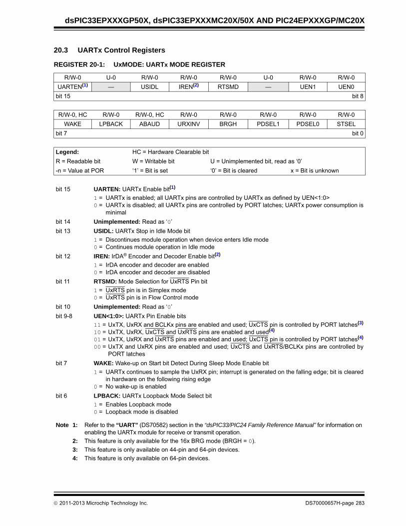
dsPIC33EPXXXGP50X, dsPIC33EPXXXMC20X/50X AND PIC24EPXXXGP/MC20X
20.3 UARTx Control Registers
REGISTER 20-1: UxMODE: UARTx MODE REGISTER
R/W-0 U-0 R/W-0 R/W-0 R/W-0 U-0 R/W-0 R/W-0
UARTEN(1) — USIDL IREN(2) RTSMD — UEN1 UEN0
bit 15 bit 8
R/W-0, HC R/W-0 R/W-0, HC R/W-0 R/W-0 R/W-0 R/W-0 R/W-0
WAKE LPBACK ABAUD URXINV BRGH PDSEL1 PDSEL0 STSEL
bit 7 bit 0
Legend: HC = Hardware Clearable bit
R = Readable bit W = Writable bit U = Unimplemented bit, read as ‘0’
-n = Value at POR ‘1’ = Bit is set ‘0’ = Bit is cleared x = Bit is unknown
bit 15 UARTEN: UARTx Enable bit(1)
1 = UARTx is enabled; all UARTx pins are controlled by UARTx as defined by UEN<1:0>0 = UARTx is disabled; all UARTx pins are controlled by PORT latches; UARTx power consumption is
minimal
bit 14 Unimplemented: Read as ‘0’
bit 13 USIDL: UARTx Stop in Idle Mode bit
1 = Discontinues module operation when device enters Idle mode0 = Continues module operation in Idle mode
bit 12 IREN: IrDA® Encoder and Decoder Enable bit(2)
1 = IrDA encoder and decoder are enabled0 = IrDA encoder and decoder are disabled
bit 11 RTSMD: Mode Selection for UxRTS Pin bit
1 = UxRTS pin is in Simplex mode0 = UxRTS pin is in Flow Control mode
bit 10 Unimplemented: Read as ‘0’
bit 9-8 UEN<1:0>: UARTx Pin Enable bits
11 = UxTX, UxRX and BCLKx pins are enabled and used; UxCTS pin is controlled by PORT latches(3)
10 = UxTX, UxRX, UxCTS and UxRTS pins are enabled and used(4)
01 = UxTX, UxRX and UxRTS pins are enabled and used; UxCTS pin is controlled by PORT latches(4)
00 = UxTX and UxRX pins are enabled and used; UxCTS and UxRTS/BCLKx pins are controlled byPORT latches
bit 7 WAKE: Wake-up on Start bit Detect During Sleep Mode Enable bit
1 = UARTx continues to sample the UxRX pin; interrupt is generated on the falling edge; bit is clearedin hardware on the following rising edge
0 = No wake-up is enabled
bit 6 LPBACK: UARTx Loopback Mode Select bit
1 = Enables Loopback mode0 = Loopback mode is disabled
Note 1: Refer to the “UART” (DS70582) section in the “dsPIC33/PIC24 Family Reference Manual” for information on enabling the UARTx module for receive or transmit operation.
2: This feature is only available for the 16x BRG mode (BRGH = 0).
3: This feature is only available on 44-pin and 64-pin devices.
4: This feature is only available on 64-pin devices.
2011-2013 Microchip Technology Inc. DS70000657H-page 283

dsPIC33EPXXXGP50X, dsPIC33EPXXXMC20X/50X AND PIC24EPXXXGP/MC20X
bit 5 ABAUD: Auto-Baud Enable bit
1 = Enables baud rate measurement on the next character – requires reception of a Sync field (55h)before other data; cleared in hardware upon completion
0 = Baud rate measurement is disabled or completed
bit 4 URXINV: UARTx Receive Polarity Inversion bit
1 = UxRX Idle state is ‘0’0 = UxRX Idle state is ‘1’
bit 3 BRGH: High Baud Rate Enable bit
1 = BRG generates 4 clocks per bit period (4x baud clock, High-Speed mode)0 = BRG generates 16 clocks per bit period (16x baud clock, Standard mode)
bit 2-1 PDSEL<1:0>: Parity and Data Selection bits
11 = 9-bit data, no parity10 = 8-bit data, odd parity01 = 8-bit data, even parity00 = 8-bit data, no parity
bit 0 STSEL: Stop Bit Selection bit
1 = Two Stop bits0 = One Stop bit
REGISTER 20-1: UxMODE: UARTx MODE REGISTER (CONTINUED)
Note 1: Refer to the “UART” (DS70582) section in the “dsPIC33/PIC24 Family Reference Manual” for information on enabling the UARTx module for receive or transmit operation.
2: This feature is only available for the 16x BRG mode (BRGH = 0).
3: This feature is only available on 44-pin and 64-pin devices.
4: This feature is only available on 64-pin devices.
DS70000657H-page 284 2011-2013 Microchip Technology Inc.

dsPIC33EPXXXGP50X, dsPIC33EPXXXMC20X/50X AND PIC24EPXXXGP/MC20X
REGISTER 20-2: UxSTA: UARTx STATUS AND CONTROL REGISTER
R/W-0 R/W-0 R/W-0 U-0 R/W-0, HC R/W-0 R-0 R-1
UTXISEL1 UTXINV UTXISEL0 — UTXBRK UTXEN(1) UTXBF TRMT
bit 15 bit 8
R/W-0 R/W-0 R/W-0 R-1 R-0 R-0 R/C-0 R-0
URXISEL1 URXISEL0 ADDEN RIDLE PERR FERR OERR URXDA
bit 7 bit 0
Legend: HC = Hardware Clearable bit C = Clearable bit
R = Readable bit W = Writable bit U = Unimplemented bit, read as ‘0’
-n = Value at POR ‘1’ = Bit is set ‘0’ = Bit is cleared x = Bit is unknown
bit 15,13 UTXISEL<1:0>: UARTx Transmission Interrupt Mode Selection bits
11 = Reserved; do not use10 = Interrupt when a character is transferred to the Transmit Shift Register (TSR) and as a result, the
transmit buffer becomes empty01 = Interrupt when the last character is shifted out of the Transmit Shift Register; all transmit operations
are completed00 = Interrupt when a character is transferred to the Transmit Shift Register (this implies there is at least
one character open in the transmit buffer)
bit 14 UTXINV: UARTx Transmit Polarity Inversion bit
If IREN = 0:1 = UxTX Idle state is ‘0’0 = UxTX Idle state is ‘1’
If IREN = 1:1 = IrDA encoded, UxTX Idle state is ‘1’0 = IrDA encoded, UxTX Idle state is ‘0’
bit 12 Unimplemented: Read as ‘0’
bit 11 UTXBRK: UARTx Transmit Break bit
1 = Sends Sync Break on next transmission – Start bit, followed by twelve ‘0’ bits, followed by Stop bit;cleared by hardware upon completion
0 = Sync Break transmission is disabled or completed
bit 10 UTXEN: UARTx Transmit Enable bit(1)
1 = Transmit is enabled, UxTX pin is controlled by UARTx0 = Transmit is disabled, any pending transmission is aborted and buffer is reset; UxTX pin is controlled
by the PORT
bit 9 UTXBF: UARTx Transmit Buffer Full Status bit (read-only)
1 = Transmit buffer is full0 = Transmit buffer is not full, at least one more character can be written
bit 8 TRMT: Transmit Shift Register Empty bit (read-only)
1 = Transmit Shift Register is empty and transmit buffer is empty (the last transmission has completed)0 = Transmit Shift Register is not empty, a transmission is in progress or queued
bit 7-6 URXISEL<1:0>: UARTx Receive Interrupt Mode Selection bits
11 = Interrupt is set on UxRSR transfer, making the receive buffer full (i.e., has 4 data characters)10 = Interrupt is set on UxRSR transfer, making the receive buffer 3/4 full (i.e., has 3 data characters)0x = Interrupt is set when any character is received and transferred from the UxRSR to the receive
buffer; receive buffer has one or more characters
Note 1: Refer to the “UART” (DS70582) section in the “dsPIC33/PIC24 Family Reference Manual” for information on enabling the UARTx module for transmit operation.
2011-2013 Microchip Technology Inc. DS70000657H-page 285

dsPIC33EPXXXGP50X, dsPIC33EPXXXMC20X/50X AND PIC24EPXXXGP/MC20X
bit 5 ADDEN: Address Character Detect bit (bit 8 of received data = 1)
1 = Address Detect mode is enabled; if 9-bit mode is not selected, this does not take effect0 = Address Detect mode is disabled
bit 4 RIDLE: Receiver Idle bit (read-only)
1 = Receiver is Idle0 = Receiver is active
bit 3 PERR: Parity Error Status bit (read-only)
1 = Parity error has been detected for the current character (character at the top of the receive FIFO)0 = Parity error has not been detected
bit 2 FERR: Framing Error Status bit (read-only)
1 = Framing error has been detected for the current character (character at the top of the receive FIFO)0 = Framing error has not been detected
bit 1 OERR: Receive Buffer Overrun Error Status bit (clear/read-only)
1 = Receive buffer has overflowed0 = Receive buffer has not overflowed; clearing a previously set OERR bit (1 0 transition) resets the
receiver buffer and the UxRSR to the empty state
bit 0 URXDA: UARTx Receive Buffer Data Available bit (read-only)
1 = Receive buffer has data, at least one more character can be read0 = Receive buffer is empty
REGISTER 20-2: UxSTA: UARTx STATUS AND CONTROL REGISTER (CONTINUED)
Note 1: Refer to the “UART” (DS70582) section in the “dsPIC33/PIC24 Family Reference Manual” for information on enabling the UARTx module for transmit operation.
DS70000657H-page 286 2011-2013 Microchip Technology Inc.

dsPIC33EPXXXGP50X, dsPIC33EPXXXMC20X/50X AND PIC24EPXXXGP/MC20X
21.0 ENHANCED CAN (ECAN™) MODULE (dsPIC33EPXXXGP/MC50X DEVICES ONLY)
21.1 Overview
The Enhanced Controller Area Network (ECAN)module is a serial interface, useful for communicat-ing with other CAN modules or microcontrollerdevices. This interface/protocol was designed toallow communications within noisy environments.The dsPIC33EPXXXGP/MC50X devices contain oneECAN module.
The ECAN module is a communication controllerimplementing the CAN 2.0 A/B protocol, as defined inthe BOSCH CAN specification. The module supportsCAN 1.2, CAN 2.0A, CAN 2.0B Passive and CAN 2.0BActive versions of the protocol. The module implemen-tation is a full CAN system. The CAN specification isnot covered within this data sheet. The reader can referto the BOSCH CAN specification for further details.
The ECAN module features are as follows:
• Implementation of the CAN protocol, CAN 1.2, CAN 2.0A and CAN 2.0B
• Standard and extended data frames
• 0-8 bytes data length
• Programmable bit rate up to 1 Mbit/sec
• Automatic response to remote transmission requests
• Up to eight transmit buffers with application speci-fied prioritization and abort capability (each buffer can contain up to 8 bytes of data)
• Up to 32 receive buffers (each buffer can contain up to 8 bytes of data)
• Up to 16 full (Standard/Extended Identifier) acceptance filters
• Three full acceptance filter masks
• DeviceNet™ addressing support
• Programmable wake-up functionality with integrated low-pass filter
• Programmable Loopback mode supports self-test operation
• Signaling via interrupt capabilities for all CAN receiver and transmitter error states
• Programmable clock source
• Programmable link to Input Capture (IC2) module for time-stamping and network synchronization
• Low-power Sleep and Idle mode
The CAN bus module consists of a protocol engine andmessage buffering/control. The CAN protocol enginehandles all functions for receiving and transmittingmessages on the CAN bus. Messages are transmittedby first loading the appropriate data registers. Statusand errors can be checked by reading the appropriateregisters. Any message detected on the CAN bus ischecked for errors and then matched against filters tosee if it should be received and stored in one of thereceive registers.
Note 1: This data sheet summarizes thefeatures of the dsPIC33EPXXXGP50X,dsPIC33EPXXXMC20X/50X andPIC24EPXXXGP/MC20X families ofdevices. It is not intended to be acomprehensive reference source. To com-plement the information in this data sheet,refer to “Enhanced Controller AreaNetwork (ECAN™)” (DS70353) in the“dsPIC33/PIC24 Family Reference Man-ual”, which is available from the Microchipweb site (www.microchip.com).
2: Some registers and associated bitsdescribed in this section may not beavailable on all devices. Refer toSection 4.0 “Memory Organization” inthis data sheet for device-specific registerand bit information.
2011-2013 Microchip Technology Inc. DS70000657H-page 287

dsPIC33EPXXXGP50X, dsPIC33EPXXXMC20X/50X AND PIC24EPXXXGP/MC20X
FIGURE 21-1: ECAN™ MODULE BLOCK DIAGRAM
Message Assembly
CAN ProtocolEngine
CxTx
Buffer
CxRx
RxF14 Filter
RxF13 Filter
RxF12 Filter
RxF11 Filter
RxF10 Filter
RxF9 Filter
RxF8 Filter
RxF7 Filter
RxF6 Filter
RxF5 Filter
RxF4 Filter
RxF3 Filter
RxF2 Filter
RxF1 Filter
RxF0 Filter
Transmit ByteSequencer
RxM1 Mask
RxM0 Mask
ControlConfiguration
Logic
CPUBus
Interrupts
TRB0 TX/RX Buffer Control Register
RxF15 Filter
RxM2 Mask
TRB7 TX/RX Buffer Control Register
TRB6 TX/RX Buffer Control Register
TRB5 TX/RX Buffer Control Register
TRB4 TX/RX Buffer Control Register
TRB3 TX/RX Buffer Control Register
TRB2 TX/RX Buffer Control Register
TRB1 TX/RX Buffer Control Register
DMA Controller
DS70000657H-page 288 2011-2013 Microchip Technology Inc.

dsPIC33EPXXXGP50X, dsPIC33EPXXXMC20X/50X AND PIC24EPXXXGP/MC20X
21.2 Modes of Operation
The ECAN module can operate in one of severaloperation modes selected by the user. These modesinclude:
• Initialization mode• Disable mode• Normal Operation mode• Listen Only mode
• Listen All Messages mode
• Loopback mode
Modes are requested by setting the REQOP<2:0> bits(CxCTRL1<10:8>). Entry into a mode is Acknowledgedby monitoring the OPMODE<2:0> bits (CxCTRL1<7:5>).The module does not change the mode and theOPMODEx bits until a change in mode is acceptable,generally during bus Idle time, which is defined as at least11 consecutive recessive bits.
21.3 ECAN Resources
Many useful resources are provided on the main prod-uct page of the Microchip web site for the devices listedin this data sheet. This product page, which can beaccessed using this link, contains the latest updatesand additional information.
21.3.1 KEY RESOURCES
• “Enhanced Controller Area Network (ECAN™)” (DS70353) in the “dsPIC33/PIC24 Family Reference Manual”
• Code Samples
• Application Notes
• Software Libraries
• Webinars
• All Related “dsPIC33/PIC24 Family Reference Manual” Sections
• Development Tools
Note: In the event you are not able to access theproduct page using the link above, enterthis URL in your browser:http://www.microchip.com/wwwproducts/Devices.aspx?dDocName=en555464
2011-2013 Microchip Technology Inc. DS70000657H-page 289
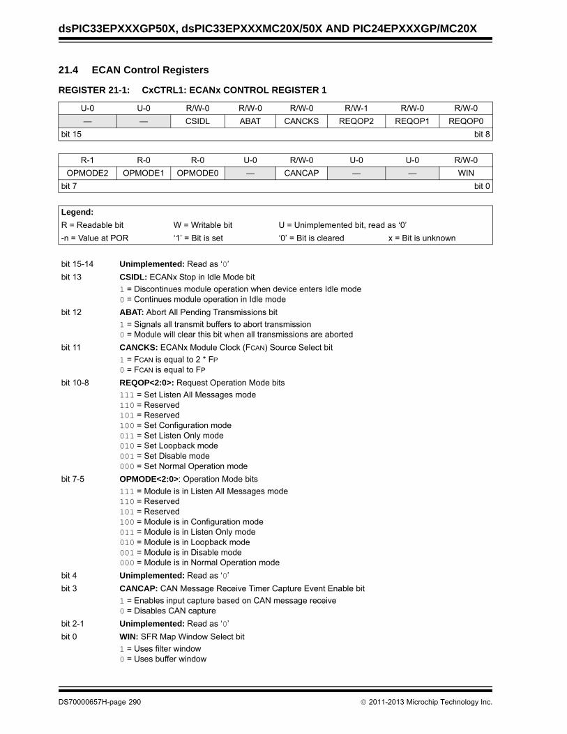
dsPIC33EPXXXGP50X, dsPIC33EPXXXMC20X/50X AND PIC24EPXXXGP/MC20X
21.4 ECAN Control Registers
REGISTER 21-1: CxCTRL1: ECANx CONTROL REGISTER 1
U-0 U-0 R/W-0 R/W-0 R/W-0 R/W-1 R/W-0 R/W-0
— — CSIDL ABAT CANCKS REQOP2 REQOP1 REQOP0
bit 15 bit 8
R-1 R-0 R-0 U-0 R/W-0 U-0 U-0 R/W-0
OPMODE2 OPMODE1 OPMODE0 — CANCAP — — WIN
bit 7 bit 0
Legend:
R = Readable bit W = Writable bit U = Unimplemented bit, read as ‘0’
-n = Value at POR ‘1’ = Bit is set ‘0’ = Bit is cleared x = Bit is unknown
bit 15-14 Unimplemented: Read as ‘0’
bit 13 CSIDL: ECANx Stop in Idle Mode bit
1 = Discontinues module operation when device enters Idle mode0 = Continues module operation in Idle mode
bit 12 ABAT: Abort All Pending Transmissions bit
1 = Signals all transmit buffers to abort transmission0 = Module will clear this bit when all transmissions are aborted
bit 11 CANCKS: ECANx Module Clock (FCAN) Source Select bit
1 = FCAN is equal to 2 * FP
0 = FCAN is equal to FP
bit 10-8 REQOP<2:0>: Request Operation Mode bits
111 = Set Listen All Messages mode110 = Reserved 101 = Reserved100 = Set Configuration mode 011 = Set Listen Only mode010 = Set Loopback mode001 = Set Disable mode000 = Set Normal Operation mode
bit 7-5 OPMODE<2:0>: Operation Mode bits
111 = Module is in Listen All Messages mode110 = Reserved101 = Reserved100 = Module is in Configuration mode011 = Module is in Listen Only mode010 = Module is in Loopback mode001 = Module is in Disable mode000 = Module is in Normal Operation mode
bit 4 Unimplemented: Read as ‘0’
bit 3 CANCAP: CAN Message Receive Timer Capture Event Enable bit
1 = Enables input capture based on CAN message receive 0 = Disables CAN capture
bit 2-1 Unimplemented: Read as ‘0’
bit 0 WIN: SFR Map Window Select bit
1 = Uses filter window 0 = Uses buffer window
DS70000657H-page 290 2011-2013 Microchip Technology Inc.

dsPIC33EPXXXGP50X, dsPIC33EPXXXMC20X/50X AND PIC24EPXXXGP/MC20X
REGISTER 21-2: CxCTRL2: ECANx CONTROL REGISTER 2
U-0 U-0 U-0 U-0 U-0 U-0 U-0 U-0
— — — — — — — —
bit 15 bit 8
U-0 U-0 U-0 R-0 R-0 R-0 R-0 R-0
— — — DNCNT4 DNCNT3 DNCNT2 DNCNT1 DNCNT0
bit 7 bit 0
Legend:
R = Readable bit W = Writable bit U = Unimplemented bit, read as ‘0’
-n = Value at POR ‘1’ = Bit is set ‘0’ = Bit is cleared x = Bit is unknown
bit 15-5 Unimplemented: Read as ‘0’
bit 4-0 DNCNT<4:0>: DeviceNet™ Filter Bit Number bits
10010-11111 = Invalid selection 10001 = Compares up to Data Byte 3, bit 6 with EID<17>
•
•
•
00001 = Compares up to Data Byte 1, bit 7 with EID<0>00000 = Does not compare data bytes
2011-2013 Microchip Technology Inc. DS70000657H-page 291

dsPIC33EPXXXGP50X, dsPIC33EPXXXMC20X/50X AND PIC24EPXXXGP/MC20X
REGISTER 21-3: CxVEC: ECANx INTERRUPT CODE REGISTER
U-0 U-0 U-0 R-0 R-0 R-0 R-0 R-0
— — — FILHIT4 FILHIT3 FILHIT2 FILHIT1 FILHIT0
bit 15 bit 8
U-0 R-1 R-0 R-0 R-0 R-0 R-0 R-0
— ICODE6 ICODE5 ICODE4 ICODE3 ICODE2 ICODE1 ICODE0
bit 7 bit 0
Legend:
R = Readable bit W = Writable bit U = Unimplemented bit, read as ‘0’
-n = Value at POR ‘1’ = Bit is set ‘0’ = Bit is cleared x = Bit is unknown
bit 15-13 Unimplemented: Read as ‘0’
bit 12-8 FILHIT<4:0>: Filter Hit Number bits
10000-11111 = Reserved01111 = Filter 15
•
•
•
00001 = Filter 100000 = Filter 0
bit 7 Unimplemented: Read as ‘0’
bit 6-0 ICODE<6:0>: Interrupt Flag Code bits
1000101-1111111 = Reserved1000100 = FIFO almost full interrupt1000011 = Receiver overflow interrupt1000010 = Wake-up interrupt1000001 = Error interrupt1000000 = No interrupt
•
•
•
0010000-0111111 = Reserved0001111 = RB15 buffer interrupt
•
•
•
0001001 = RB9 buffer interrupt 0001000 = RB8 buffer interrupt 0000111 = TRB7 buffer interrupt0000110 = TRB6 buffer interrupt0000101 = TRB5 buffer interrupt0000100 = TRB4 buffer interrupt0000011 = TRB3 buffer interrupt0000010 = TRB2 buffer interrupt0000001 = TRB1 buffer interrupt0000000 = TRB0 buffer interrupt
DS70000657H-page 292 2011-2013 Microchip Technology Inc.
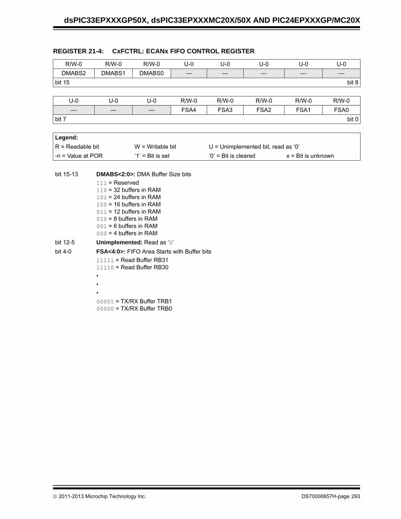
dsPIC33EPXXXGP50X, dsPIC33EPXXXMC20X/50X AND PIC24EPXXXGP/MC20X
REGISTER 21-4: CxFCTRL: ECANx FIFO CONTROL REGISTER
R/W-0 R/W-0 R/W-0 U-0 U-0 U-0 U-0 U-0
DMABS2 DMABS1 DMABS0 — — — — —
bit 15 bit 8
U-0 U-0 U-0 R/W-0 R/W-0 R/W-0 R/W-0 R/W-0
— — — FSA4 FSA3 FSA2 FSA1 FSA0
bit 7 bit 0
Legend:
R = Readable bit W = Writable bit U = Unimplemented bit, read as ‘0’
-n = Value at POR ‘1’ = Bit is set ‘0’ = Bit is cleared x = Bit is unknown
bit 15-13 DMABS<2:0>: DMA Buffer Size bits
111 = Reserved110 = 32 buffers in RAM101 = 24 buffers in RAM100 = 16 buffers in RAM011 = 12 buffers in RAM010 = 8 buffers in RAM001 = 6 buffers in RAM000 = 4 buffers in RAM
bit 12-5 Unimplemented: Read as ‘0’
bit 4-0 FSA<4:0>: FIFO Area Starts with Buffer bits
11111 = Read Buffer RB31 11110 = Read Buffer RB30
•
•
•
00001 = TX/RX Buffer TRB100000 = TX/RX Buffer TRB0
2011-2013 Microchip Technology Inc. DS70000657H-page 293

dsPIC33EPXXXGP50X, dsPIC33EPXXXMC20X/50X AND PIC24EPXXXGP/MC20X
REGISTER 21-5: CxFIFO: ECANx FIFO STATUS REGISTER
U-0 U-0 R-0 R-0 R-0 R-0 R-0 R-0
— — FBP5 FBP4 FBP3 FBP2 FBP1 FBP0
bit 15 bit 8
U-0 U-0 R-0 R-0 R-0 R-0 R-0 R-0
— — FNRB5 FNRB4 FNRB3 FNRB2 FNRB1 FNRB0
bit 7 bit 0
Legend:
R = Readable bit W = Writable bit U = Unimplemented bit, read as ‘0’
-n = Value at POR ‘1’ = Bit is set ‘0’ = Bit is cleared x = Bit is unknown
bit 15-14 Unimplemented: Read as ‘0’
bit 13-8 FBP<5:0>: FIFO Buffer Pointer bits
011111 = RB31 buffer011110 = RB30 buffer
•
•
•
000001 = TRB1 buffer000000 = TRB0 buffer
bit 7-6 Unimplemented: Read as ‘0’
bit 5-0 FNRB<5:0>: FIFO Next Read Buffer Pointer bits
011111 = RB31 buffer011110 = RB30 buffer
•
•
•
000001 = TRB1 buffer000000 = TRB0 buffer
DS70000657H-page 294 2011-2013 Microchip Technology Inc.

dsPIC33EPXXXGP50X, dsPIC33EPXXXMC20X/50X AND PIC24EPXXXGP/MC20X
REGISTER 21-6: CxINTF: ECANx INTERRUPT FLAG REGISTER
U-0 U-0 R-0 R-0 R-0 R-0 R-0 R-0
— — TXBO TXBP RXBP TXWAR RXWAR EWARN
bit 15 bit 8
R/C-0 R/C-0 R/C-0 U-0 R/C-0 R/C-0 R/C-0 R/C-0
IVRIF WAKIF ERRIF — FIFOIF RBOVIF RBIF TBIF
bit 7 bit 0
Legend: C = Writable bit, but only ‘0’ can be written to clear the bit
R = Readable bit W = Writable bit U = Unimplemented bit, read as ‘0’
-n = Value at POR ‘1’ = Bit is set ‘0’ = Bit is cleared x = Bit is unknown
bit 15-14 Unimplemented: Read as ‘0’
bit 13 TXBO: Transmitter in Error State Bus Off bit
1 = Transmitter is in Bus Off state0 = Transmitter is not in Bus Off state
bit 12 TXBP: Transmitter in Error State Bus Passive bit
1 = Transmitter is in Bus Passive state0 = Transmitter is not in Bus Passive state
bit 11 RXBP: Receiver in Error State Bus Passive bit
1 = Receiver is in Bus Passive state0 = Receiver is not in Bus Passive state
bit 10 TXWAR: Transmitter in Error State Warning bit
1 = Transmitter is in Error Warning state0 = Transmitter is not in Error Warning state
bit 9 RXWAR: Receiver in Error State Warning bit
1 = Receiver is in Error Warning state0 = Receiver is not in Error Warning state
bit 8 EWARN: Transmitter or Receiver in Error State Warning bit
1 = Transmitter or receiver is in Error Warning state0 = Transmitter or receiver is not in Error Warning state
bit 7 IVRIF: Invalid Message Interrupt Flag bit
1 = Interrupt request has occurred0 = Interrupt request has not occurred
bit 6 WAKIF: Bus Wake-up Activity Interrupt Flag bit
1 = Interrupt request has occurred0 = Interrupt request has not occurred
bit 5 ERRIF: Error Interrupt Flag bit (multiple sources in CxINTF<13:8>)
1 = Interrupt request has occurred0 = Interrupt request has not occurred
bit 4 Unimplemented: Read as ‘0’
bit 3 FIFOIF: FIFO Almost Full Interrupt Flag bit
1 = Interrupt request has occurred0 = Interrupt request has not occurred
bit 2 RBOVIF: RX Buffer Overflow Interrupt Flag bit
1 = Interrupt request has occurred0 = Interrupt request has not occurred
2011-2013 Microchip Technology Inc. DS70000657H-page 295
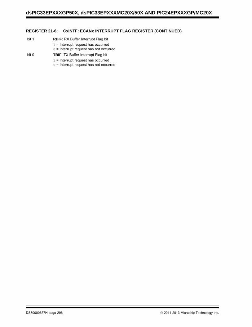
dsPIC33EPXXXGP50X, dsPIC33EPXXXMC20X/50X AND PIC24EPXXXGP/MC20X
bit 1 RBIF: RX Buffer Interrupt Flag bit
1 = Interrupt request has occurred0 = Interrupt request has not occurred
bit 0 TBIF: TX Buffer Interrupt Flag bit
1 = Interrupt request has occurred0 = Interrupt request has not occurred
REGISTER 21-6: CxINTF: ECANx INTERRUPT FLAG REGISTER (CONTINUED)
DS70000657H-page 296 2011-2013 Microchip Technology Inc.

dsPIC33EPXXXGP50X, dsPIC33EPXXXMC20X/50X AND PIC24EPXXXGP/MC20X
REGISTER 21-7: CxINTE: ECANx INTERRUPT ENABLE REGISTER
U-0 U-0 U-0 U-0 U-0 U-0 U-0 U-0
— — — — — — — —
bit 15 bit 8
R/W-0 R/W-0 R/W-0 U-0 R/W-0 R/W-0 R/W-0 R/W-0
IVRIE WAKIE ERRIE — FIFOIE RBOVIE RBIE TBIE
bit 7 bit 0
Legend:
R = Readable bit W = Writable bit U = Unimplemented bit, read as ‘0’
-n = Value at POR ‘1’ = Bit is set ‘0’ = Bit is cleared x = Bit is unknown
bit 15-8 Unimplemented: Read as ‘0’
bit 7 IVRIE: Invalid Message Interrupt Enable bit
1 = Interrupt request is enabled0 = Interrupt request is not enabled
bit 6 WAKIE: Bus Wake-up Activity Interrupt Enable bit
1 = Interrupt request is enabled0 = Interrupt request is not enabled
bit 5 ERRIE: Error Interrupt Enable bit
1 = Interrupt request is enabled0 = Interrupt request is not enabled
bit 4 Unimplemented: Read as ‘0’
bit 3 FIFOIE: FIFO Almost Full Interrupt Enable bit
1 = Interrupt request is enabled0 = Interrupt request is not enabled
bit 2 RBOVIE: RX Buffer Overflow Interrupt Enable bit
1 = Interrupt request is enabled0 = Interrupt request is not enabled
bit 1 RBIE: RX Buffer Interrupt Enable bit
1 = Interrupt request is enabled0 = Interrupt request is not enabled
bit 0 TBIE: TX Buffer Interrupt Enable bit
1 = Interrupt request is enabled0 = Interrupt request is not enabled
2011-2013 Microchip Technology Inc. DS70000657H-page 297

dsPIC33EPXXXGP50X, dsPIC33EPXXXMC20X/50X AND PIC24EPXXXGP/MC20X
REGISTER 21-8: CxEC: ECANx TRANSMIT/RECEIVE ERROR COUNT REGISTER
R-0 R-0 R-0 R-0 R-0 R-0 R-0 R-0
TERRCNT<7:0>
bit 15 bit 8
R-0 R-0 R-0 R-0 R-0 R-0 R-0 R-0
RERRCNT<7:0>
bit 7 bit 0
Legend:
R = Readable bit W = Writable bit U = Unimplemented bit, read as ‘0’
-n = Value at POR ‘1’ = Bit is set ‘0’ = Bit is cleared x = Bit is unknown
bit 15-8 TERRCNT<7:0>: Transmit Error Count bits
bit 7-0 RERRCNT<7:0>: Receive Error Count bits
REGISTER 21-9: CxCFG1: ECANx BAUD RATE CONFIGURATION REGISTER 1
U-0 U-0 U-0 U-0 U-0 U-0 U-0 U-0
— — — — — — — —
bit 15 bit 8
R/W-0 R/W-0 R/W-0 R/W-0 R/W-0 R/W-0 R/W-0 R/W-0
SJW1 SJW0 BRP5 BRP4 BRP3 BRP2 BRP1 BRP0
bit 7 bit 0
Legend:
R = Readable bit W = Writable bit U = Unimplemented bit, read as ‘0’
-n = Value at POR ‘1’ = Bit is set ‘0’ = Bit is cleared x = Bit is unknown
bit 15-8 Unimplemented: Read as ‘0’
bit 7-6 SJW<1:0>: Synchronization Jump Width bits
11 = Length is 4 x TQ 10 = Length is 3 x TQ 01 = Length is 2 x TQ 00 = Length is 1 x TQ
bit 5-0 BRP<5:0>: Baud Rate Prescaler bits
11 1111 = TQ = 2 x 64 x 1/FCAN
•
•
•
00 0010 = TQ = 2 x 3 x 1/FCAN
00 0001 = TQ = 2 x 2 x 1/FCAN 00 0000 = TQ = 2 x 1 x 1/FCAN
DS70000657H-page 298 2011-2013 Microchip Technology Inc.

dsPIC33EPXXXGP50X, dsPIC33EPXXXMC20X/50X AND PIC24EPXXXGP/MC20X
REGISTER 21-10: CxCFG2: ECANx BAUD RATE CONFIGURATION REGISTER 2
U-0 R/W-x U-0 U-0 U-0 R/W-x R/W-x R/W-x
— WAKFIL — — — SEG2PH2 SEG2PH1 SEG2PH0
bit 15 bit 8
R/W-x R/W-x R/W-x R/W-x R/W-x R/W-x R/W-x R/W-x
SEG2PHTS SAM SEG1PH2 SEG1PH1 SEG1PH0 PRSEG2 PRSEG1 PRSEG0
bit 7 bit 0
Legend:
R = Readable bit W = Writable bit U = Unimplemented bit, read as ‘0’
-n = Value at POR ‘1’ = Bit is set ‘0’ = Bit is cleared x = Bit is unknown
bit 15 Unimplemented: Read as ‘0’
bit 14 WAKFIL: Select CAN Bus Line Filter for Wake-up bit
1 = Uses CAN bus line filter for wake-up0 = CAN bus line filter is not used for wake-up
bit 13-11 Unimplemented: Read as ‘0’
bit 10-8 SEG2PH<2:0>: Phase Segment 2 bits
111 = Length is 8 x TQ
•
•
•
000 = Length is 1 x TQ
bit 7 SEG2PHTS: Phase Segment 2 Time Select bit
1 = Freely programmable0 = Maximum of SEG1PHx bits or Information Processing Time (IPT), whichever is greater
bit 6 SAM: Sample of the CAN Bus Line bit
1 = Bus line is sampled three times at the sample point 0 = Bus line is sampled once at the sample point
bit 5-3 SEG1PH<2:0>: Phase Segment 1 bits
111 = Length is 8 x TQ
•
•
•
000 = Length is 1 x TQ
bit 2-0 PRSEG<2:0>: Propagation Time Segment bits
111 = Length is 8 x TQ
•
•
•
000 = Length is 1 x TQ
2011-2013 Microchip Technology Inc. DS70000657H-page 299

dsPIC33EPXXXGP50X, dsPIC33EPXXXMC20X/50X AND PIC24EPXXXGP/MC20X
REGISTER 21-11: CxFEN1: ECANx ACCEPTANCE FILTER ENABLE REGISTER 1
R/W-1 R/W-1 R/W-1 R/W-1 R/W-1 R/W-1 R/W-1 R/W-1
FLTEN15 FLTEN14 FLTEN13 FLTEN12 FLTEN11 FLTEN10 FLTEN9 FLTEN8
bit 15 bit 8
R/W-1 R/W-1 R/W-1 R/W-1 R/W-1 R/W-1 R/W-1 R/W-1
FLTEN7 FLTEN6 FLTEN5 FLTEN4 FLTEN3 FLTEN2 FLTEN1 FLTEN0
bit 7 bit 0
Legend:
R = Readable bit W = Writable bit U = Unimplemented bit, read as ‘0’
-n = Value at POR ‘1’ = Bit is set ‘0’ = Bit is cleared x = Bit is unknown
bit 15-0 FLTEN<15:0>: Enable Filter n to Accept Messages bits
1 = Enables Filter n0 = Disables Filter n
REGISTER 21-12: CxBUFPNT1: ECANx FILTER 0-3 BUFFER POINTER REGISTER 1
R/W-0 R/W-0 R/W-0 R/W-0 R/W-0 R/W-0 R/W-0 R/W-0
F3BP<3:0> F2BP<3:0>
bit 15 bit 8
R/W-0 R/W-0 R/W-0 R/W-0 R/W-0 R/W-0 R/W-0 R/W-0
F1BP<3:0> F0BP<3:0>
bit 7 bit 0
Legend:
R = Readable bit W = Writable bit U = Unimplemented bit, read as ‘0’
-n = Value at POR ‘1’ = Bit is set ‘0’ = Bit is cleared x = Bit is unknown
bit 15-12 F3BP<3:0>: RX Buffer Mask for Filter 3 bits
1111 = Filter hits received in RX FIFO buffer1110 = Filter hits received in RX Buffer 14•••0001 = Filter hits received in RX Buffer 10000 = Filter hits received in RX Buffer 0
bit 11-8 F2BP<3:0>: RX Buffer Mask for Filter 2 bits (same values as bits<15:12>)
bit 7-4 F1BP<3:0>: RX Buffer Mask for Filter 1 bits (same values as bits<15:12>)
bit 3-0 F0BP<3:0>: RX Buffer Mask for Filter 0 bits (same values as bits<15:12>)
DS70000657H-page 300 2011-2013 Microchip Technology Inc.

dsPIC33EPXXXGP50X, dsPIC33EPXXXMC20X/50X AND PIC24EPXXXGP/MC20X
REGISTER 21-13: CxBUFPNT2: ECANx FILTER 4-7 BUFFER POINTER REGISTER 2
R/W-0 R/W-0 R/W-0 R/W-0 R/W-0 R/W-0 R/W-0 R/W-0
F7BP<3:0> F6BP<3:0>
bit 15 bit 8
R/W-0 R/W-0 R/W-0 R/W-0 R/W-0 R/W-0 R/W-0 R/W-0
F5BP<3:0> F4BP<3:0>
bit 7 bit 0
Legend:
R = Readable bit W = Writable bit U = Unimplemented bit, read as ‘0’
-n = Value at POR ‘1’ = Bit is set ‘0’ = Bit is cleared x = Bit is unknown
bit 15-12 F7BP<3:0>: RX Buffer Mask for Filter 7 bits
1111 = Filter hits received in RX FIFO buffer1110 = Filter hits received in RX Buffer 14•••0001 = Filter hits received in RX Buffer 10000 = Filter hits received in RX Buffer 0
bit 11-8 F6BP<3:0>: RX Buffer Mask for Filter 6 bits (same values as bits<15:12>)
bit 7-4 F5BP<3:0>: RX Buffer Mask for Filter 5 bits (same values as bits<15:12>)
bit 3-0 F4BP<3:0>: RX Buffer Mask for Filter 4 bits (same values as bits<15:12>)
REGISTER 21-14: CxBUFPNT3: ECANx FILTER 8-11 BUFFER POINTER REGISTER 3
R/W-0 R/W-0 R/W-0 R/W-0 R/W-0 R/W-0 R/W-0 R/W-0
F11BP<3:0> F10BP<3:0>
bit 15 bit 8
R/W-0 R/W-0 R/W-0 R/W-0 R/W-0 R/W-0 R/W-0 R/W-0
F9BP<3:0> F8BP<3:0>
bit 7 bit 0
Legend:
R = Readable bit W = Writable bit U = Unimplemented bit, read as ‘0’
-n = Value at POR ‘1’ = Bit is set ‘0’ = Bit is cleared x = Bit is unknown
bit 15-12 F11BP<3:0>: RX Buffer Mask for Filter 11 bits
1111 = Filter hits received in RX FIFO buffer1110 = Filter hits received in RX Buffer 14•••0001 = Filter hits received in RX Buffer 10000 = Filter hits received in RX Buffer 0
bit 11-8 F10BP<3:0>: RX Buffer Mask for Filter 10 bits (same values as bits<15:12>)
bit 7-4 F9BP<3:0>: RX Buffer Mask for Filter 9 bits (same values as bits<15:12>)
bit 3-0 F8BP<3:0>: RX Buffer Mask for Filter 8 bits (same values as bits<15:12>)
2011-2013 Microchip Technology Inc. DS70000657H-page 301

dsPIC33EPXXXGP50X, dsPIC33EPXXXMC20X/50X AND PIC24EPXXXGP/MC20X
REGISTER 21-15: CxBUFPNT4: ECANx FILTER 12-15 BUFFER POINTER REGISTER 4
R/W-0 R/W-0 R/W-0 R/W-0 R/W-0 R/W-0 R/W-0 R/W-0
F15BP<3:0> F14BP<3:0>
bit 15 bit 8
R/W-0 R/W-0 R/W-0 R/W-0 R/W-0 R/W-0 R/W-0 R/W-0
F13BP<3:0> F12BP<3:0>
bit 7 bit 0
Legend:
R = Readable bit W = Writable bit U = Unimplemented bit, read as ‘0’
-n = Value at POR ‘1’ = Bit is set ‘0’ = Bit is cleared x = Bit is unknown
bit 15-12 F15BP<3:0>: RX Buffer Mask for Filter 15 bits
1111 = Filter hits received in RX FIFO buffer1110 = Filter hits received in RX Buffer 14•••0001 = Filter hits received in RX Buffer 10000 = Filter hits received in RX Buffer 0
bit 11-8 F14BP<3:0>: RX Buffer Mask for Filter 14 bits (same values as bits<15:12>)
bit 7-4 F13BP<3:0>: RX Buffer Mask for Filter 13 bits (same values as bits<15:12>)
bit 3-0 F12BP<3:0>: RX Buffer Mask for Filter 12 bits (same values as bits<15:12>)
DS70000657H-page 302 2011-2013 Microchip Technology Inc.

dsPIC33EPXXXGP50X, dsPIC33EPXXXMC20X/50X AND PIC24EPXXXGP/MC20X
REGISTER 21-16: CxRXFnSID: ECANx ACCEPTANCE FILTER n STANDARD IDENTIFIER REGISTER (n = 0-15)
R/W-x R/W-x R/W-x R/W-x R/W-x R/W-x R/W-x R/W-x
SID10 SID9 SID8 SID7 SID6 SID5 SID4 SID3
bit 15 bit 8
R/W-x R/W-x R/W-x U-0 R/W-x U-0 R/W-x R/W-x
SID2 SID1 SID0 — EXIDE — EID17 EID16
bit 7 bit 0
Legend:
R = Readable bit W = Writable bit U = Unimplemented bit, read as ‘0’
-n = Value at POR ‘1’ = Bit is set ‘0’ = Bit is cleared x = Bit is unknown
bit 15-5 SID<10:0>: Standard Identifier bits
1 = Message address bit, SIDx, must be ‘1’ to match filter0 = Message address bit, SIDx, must be ‘0’ to match filter
bit 4 Unimplemented: Read as ‘0’
bit 3 EXIDE: Extended Identifier Enable bit
If MIDE = 1:1 = Matches only messages with Extended Identifier addresses0 = Matches only messages with Standard Identifier addresses
If MIDE = 0:Ignores EXIDE bit.
bit 2 Unimplemented: Read as ‘0’
bit 1-0 EID<17:16>: Extended Identifier bits
1 = Message address bit, EIDx, must be ‘1’ to match filter0 = Message address bit, EIDx, must be ‘0’ to match filter
2011-2013 Microchip Technology Inc. DS70000657H-page 303

dsPIC33EPXXXGP50X, dsPIC33EPXXXMC20X/50X AND PIC24EPXXXGP/MC20X
REGISTER 21-17: CxRXFnEID: ECANx ACCEPTANCE FILTER n EXTENDED IDENTIFIER REGISTER (n = 0-15)
R/W-x R/W-x R/W-x R/W-x R/W-x R/W-x R/W-x R/W-x
EID15 EID14 EID13 EID12 EID11 EID10 EID9 EID8
bit 15 bit 8
R/W-x R/W-x R/W-x R/W-x R/W-x R/W-x R/W-x R/W-x
EID7 EID6 EID5 EID4 EID3 EID2 EID1 EID0
bit 7 bit 0
Legend:
R = Readable bit W = Writable bit U = Unimplemented bit, read as ‘0’
-n = Value at POR ‘1’ = Bit is set ‘0’ = Bit is cleared x = Bit is unknown
bit 15-0 EID<15:0>: Extended Identifier bits
1 = Message address bit, EIDx, must be ‘1’ to match filter0 = Message address bit, EIDx, must be ‘0’ to match filter
REGISTER 21-18: CxFMSKSEL1: ECANx FILTER 7-0 MASK SELECTION REGISTER 1
R/W-0 R/W-0 R/W-0 R/W-0 R/W-0 R/W-0 R/W-0 R/W-0
F7MSK<1:0> F6MSK<1:0> F5MSK<1:0> F4MSK<1:0>
bit 15 bit 8
R/W-0 R/W-0 R/W-0 R/W-0 R/W-0 R/W-0 R/W-0 R/W-0
F3MSK<1:0> F2MSK<1:0> F1MSK<1:0> F0MSK<1:0>
bit 7 bit 0
Legend:
R = Readable bit W = Writable bit U = Unimplemented bit, read as ‘0’
-n = Value at POR ‘1’ = Bit is set ‘0’ = Bit is cleared x = Bit is unknown
bit 15-14 F7MSK<1:0>: Mask Source for Filter 7 bits
11 = Reserved10 = Acceptance Mask 2 registers contain mask01 = Acceptance Mask 1 registers contain mask00 = Acceptance Mask 0 registers contain mask
bit 13-12 F6MSK<1:0>: Mask Source for Filter 6 bits (same values as bits<15:14>)
bit 11-10 F5MSK<1:0>: Mask Source for Filter 5 bits (same values as bits<15:14>)
bit 9-8 F4MSK<1:0>: Mask Source for Filter 4 bits (same values as bits<15:14>)
bit 7-6 F3MSK<1:0>: Mask Source for Filter 3 bits (same values as bits<15:14>)
bit 5-4 F2MSK<1:0>: Mask Source for Filter 2 bits (same values as bits<15:14>)
bit 3-2 F1MSK<1:0>: Mask Source for Filter 1 bits (same values as bits<15:14>)
bit 1-0 F0MSK<1:0>: Mask Source for Filter 0 bits (same values as bits<15:14>)
DS70000657H-page 304 2011-2013 Microchip Technology Inc.
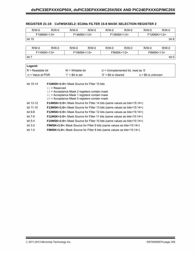
dsPIC33EPXXXGP50X, dsPIC33EPXXXMC20X/50X AND PIC24EPXXXGP/MC20X
REGISTER 21-19: CxFMSKSEL2: ECANx FILTER 15-8 MASK SELECTION REGISTER 2
R/W-0 R/W-0 R/W-0 R/W-0 R/W-0 R/W-0 R/W-0 R/W-0
F15MSK<1:0> F14MSK<1:0> F13MSK<1:0> F12MSK<1:0>
bit 15 bit 8
R/W-0 R/W-0 R/W-0 R/W-0 R/W-0 R/W-0 R/W-0 R/W-0
F11MSK<1:0> F10MSK<1:0> F9MSK<1:0> F8MSK<1:0>
bit 7 bit 0
Legend:
R = Readable bit W = Writable bit U = Unimplemented bit, read as ‘0’
-n = Value at POR ‘1’ = Bit is set ‘0’ = Bit is cleared x = Bit is unknown
bit 15-14 F15MSK<1:0>: Mask Source for Filter 15 bits
11 = Reserved10 = Acceptance Mask 2 registers contain mask01 = Acceptance Mask 1 registers contain mask00 = Acceptance Mask 0 registers contain mask
bit 13-12 F14MSK<1:0>: Mask Source for Filter 14 bits (same values as bits<15:14>)
bit 11-10 F13MSK<1:0>: Mask Source for Filter 13 bits (same values as bits<15:14>)
bit 9-8 F12MSK<1:0>: Mask Source for Filter 12 bits (same values as bits<15:14>)
bit 7-6 F11MSK<1:0>: Mask Source for Filter 11 bits (same values as bits<15:14>)
bit 5-4 F10MSK<1:0>: Mask Source for Filter 10 bits (same values as bits<15:14>)
bit 3-2 F9MSK<1:0>: Mask Source for Filter 9 bits (same values as bits<15:14>)
bit 1-0 F8MSK<1:0>: Mask Source for Filter 8 bits (same values as bits<15:14>)
2011-2013 Microchip Technology Inc. DS70000657H-page 305

dsPIC33EPXXXGP50X, dsPIC33EPXXXMC20X/50X AND PIC24EPXXXGP/MC20X
REGISTER 21-20: CxRXMnSID: ECANx ACCEPTANCE FILTER MASK n STANDARD IDENTIFIER REGISTER (n = 0-2)
R/W-x R/W-x R/W-x R/W-x R/W-x R/W-x R/W-x R/W-x
SID10 SID9 SID8 SID7 SID6 SID5 SID4 SID3
bit 15 bit 8
R/W-x R/W-x R/W-x U-0 R/W-x U-0 R/W-x R/W-x
SID2 SID1 SID0 — MIDE — EID17 EID16
bit 7 bit 0
Legend:
R = Readable bit W = Writable bit U = Unimplemented bit, read as ‘0’
-n = Value at POR ‘1’ = Bit is set ‘0’ = Bit is cleared x = Bit is unknown
bit 15-5 SID<10:0>: Standard Identifier bits
1 = Includes bit, SIDx, in filter comparison0 = SIDx bit is a don’t care in filter comparison
bit 4 Unimplemented: Read as ‘0’
bit 3 MIDE: Identifier Receive Mode bit
1 = Matches only message types (standard or extended address) that correspond to EXIDE bit in the filter0 = Matches either standard or extended address message if filters match (i.e., if (Filter SID) = (Message
SID) or if (Filter SID/EID) = (Message SID/EID))
bit 2 Unimplemented: Read as ‘0’
bit 1-0 EID<17:16>: Extended Identifier bits
1 = Includes bit, EIDx, in filter comparison0 = EIDx bit is a don’t care in filter comparison
REGISTER 21-21: CxRXMnEID: ECANx ACCEPTANCE FILTER MASK n EXTENDED IDENTIFIER REGISTER (n = 0-2)
R/W-x R/W-x R/W-x R/W-x R/W-x R/W-x R/W-x R/W-x
EID15 EID14 EID13 EID12 EID11 EID10 EID9 EID8
bit 15 bit 8
R/W-x R/W-x R/W-x R/W-x R/W-x R/W-x R/W-x R/W-x
EID7 EID6 EID5 EID4 EID3 EID2 EID1 EID0
bit 7 bit 0
Legend:
R = Readable bit W = Writable bit U = Unimplemented bit, read as ‘0’
-n = Value at POR ‘1’ = Bit is set ‘0’ = Bit is cleared x = Bit is unknown
bit 15-0 EID<15:0>: Extended Identifier bits
1 = Includes bit, EIDx, in filter comparison0 = EIDx bit is a don’t care in filter comparison
DS70000657H-page 306 2011-2013 Microchip Technology Inc.

dsPIC33EPXXXGP50X, dsPIC33EPXXXMC20X/50X AND PIC24EPXXXGP/MC20X
REGISTER 21-22: CxRXFUL1: ECANx RECEIVE BUFFER FULL REGISTER 1
R/C-0 R/C-0 R/C-0 R/C-0 R/C-0 R/C-0 R/C-0 R/C-0
RXFUL15 RXFUL14 RXFUL13 RXFUL12 RXFUL11 RXFUL10 RXFUL9 RXFUL8
bit 15 bit 8
R/C-0 R/C-0 R/C-0 R/C-0 R/C-0 R/C-0 R/C-0 R/C-0
RXFUL7 RXFUL6 RXFUL5 RXFUL4 RXFUL3 RXFUL2 RXFUL1 RXFUL0
bit 7 bit 0
Legend: C = Writable bit, but only ‘0’ can be written to clear the bit
R = Readable bit W = Writable bit U = Unimplemented bit, read as ‘0’
-n = Value at POR ‘1’ = Bit is set ‘0’ = Bit is cleared x = Bit is unknown
bit 15-0 RXFUL<15:0>: Receive Buffer n Full bits
1 = Buffer is full (set by module) 0 = Buffer is empty (cleared by user software)
REGISTER 21-23: CxRXFUL2: ECANx RECEIVE BUFFER FULL REGISTER 2
R/C-0 R/C-0 R/C-0 R/C-0 R/C-0 R/C-0 R/C-0 R/C-0
RXFUL31 RXFUL30 RXFUL29 RXFUL28 RXFUL27 RXFUL26 RXFUL25 RXFUL24
bit 15 bit 8
R/C-0 R/C-0 R/C-0 R/C-0 R/C-0 R/C-0 R/C-0 R/C-0
RXFUL23 RXFUL22 RXFUL21 RXFUL20 RXFUL19 RXFUL18 RXFUL17 RXFUL16
bit 7 bit 0
Legend: C = Writable bit, but only ‘0’ can be written to clear the bit
R = Readable bit W = Writable bit U = Unimplemented bit, read as ‘0’
-n = Value at POR ‘1’ = Bit is set ‘0’ = Bit is cleared x = Bit is unknown
bit 15-0 RXFUL<31:16>: Receive Buffer n Full bits
1 = Buffer is full (set by module) 0 = Buffer is empty (cleared by user software)
2011-2013 Microchip Technology Inc. DS70000657H-page 307

dsPIC33EPXXXGP50X, dsPIC33EPXXXMC20X/50X AND PIC24EPXXXGP/MC20X
REGISTER 21-24: CxRXOVF1: ECANx RECEIVE BUFFER OVERFLOW REGISTER 1
R/C-0 R/C-0 R/C-0 R/C-0 R/C-0 R/C-0 R/C-0 R/C-0
RXOVF15 RXOVF14 RXOVF13 RXOVF12 RXOVF11 RXOVF10 RXOVF9 RXOVF8
bit 15 bit 8
R/C-0 R/C-0 R/C-0 R/C-0 R/C-0 R/C-0 R/C-0 R/C-0
RXOVF7 RXOVF6 RXOVF5 RXOVF4 RXOVF3 RXOVF2 RXOVF1 RXOVF0
bit 7 bit 0
Legend: C = Writable bit, but only ‘0’ can be written to clear the bit
R = Readable bit W = Writable bit U = Unimplemented bit, read as ‘0’
-n = Value at POR ‘1’ = Bit is set ‘0’ = Bit is cleared x = Bit is unknown
bit 15-0 RXOVF<15:0>: Receive Buffer n Overflow bits
1 = Module attempted to write to a full buffer (set by module) 0 = No overflow condition (cleared by user software)
REGISTER 21-25: CxRXOVF2: ECANx RECEIVE BUFFER OVERFLOW REGISTER 2
R/C-0 R/C-0 R/C-0 R/C-0 R/C-0 R/C-0 R/C-0 R/C-0
RXOVF31 RXOVF30 RXOVF29 RXOVF28 RXOVF27 RXOVF26 RXOVF25 RXOVF24
bit 15 bit 8
R/C-0 R/C-0 R/C-0 R/C-0 R/C-0 R/C-0 R/C-0 R/C-0
RXOVF23 RXOVF22 RXOVF21 RXOVF20 RXOVF19 RXOVF18 RXOVF17 RXOVF16
bit 7 bit 0
Legend: C = Writable bit, but only ‘0’ can be written to clear the bit
R = Readable bit W = Writable bit U = Unimplemented bit, read as ‘0’
-n = Value at POR ‘1’ = Bit is set ‘0’ = Bit is cleared x = Bit is unknown
bit 15-0 RXOVF<31:16>: Receive Buffer n Overflow bits
1 = Module attempted to write to a full buffer (set by module) 0 = No overflow condition (cleared by user software)
DS70000657H-page 308 2011-2013 Microchip Technology Inc.

dsPIC33EPXXXGP50X, dsPIC33EPXXXMC20X/50X AND PIC24EPXXXGP/MC20X
REGISTER 21-26: CxTRmnCON: ECANx TX/RX BUFFER mn CONTROL REGISTER(m = 0,2,4,6; n = 1,3,5,7)
R/W-0 R-0 R-0 R-0 R/W-0 R/W-0 R/W-0 R/W-0
TXENn TXABTn TXLARBn TXERRn TXREQn RTRENn TXnPRI1 TXnPRI0
bit 15 bit 8
R/W-0 R-0 R-0 R-0 R/W-0 R/W-0 R/W-0 R/W-0
TXENm TXABTm(1) TXLARBm(1) TXERRm(1) TXREQm RTRENm TXmPRI1 TXmPRI0
bit 7 bit 0
Legend:
R = Readable bit W = Writable bit U = Unimplemented bit, read as ‘0’
-n = Value at POR ‘1’ = Bit is set ‘0’ = Bit is cleared x = Bit is unknown
bit 15-8 See Definition for bits<7:0>, Controls Buffer n
bit 7 TXENm: TX/RX Buffer Selection bit
1 = Buffer TRBn is a transmit buffer0 = Buffer TRBn is a receive buffer
bit 6 TXABTm: Message Aborted bit(1)
1 = Message was aborted0 = Message completed transmission successfully
bit 5 TXLARBm: Message Lost Arbitration bit(1)
1 = Message lost arbitration while being sent0 = Message did not lose arbitration while being sent
bit 4 TXERRm: Error Detected During Transmission bit(1)
1 = A bus error occurred while the message was being sent0 = A bus error did not occur while the message was being sent
bit 3 TXREQm: Message Send Request bit
1 = Requests that a message be sent; the bit automatically clears when the message is successfullysent
0 = Clearing the bit to ‘0’ while set requests a message abort
bit 2 RTRENm: Auto-Remote Transmit Enable bit
1 = When a remote transmit is received, TXREQ will be set0 = When a remote transmit is received, TXREQ will be unaffected
bit 1-0 TXmPRI<1:0>: Message Transmission Priority bits
11 = Highest message priority10 = High intermediate message priority01 = Low intermediate message priority00 = Lowest message priority
Note 1: This bit is cleared when TXREQ is set.
Note: The buffers, SID, EID, DLC, Data Field, and Receive Status registers are located in DMA RAM.
2011-2013 Microchip Technology Inc. DS70000657H-page 309

dsPIC33EPXXXGP50X, dsPIC33EPXXXMC20X/50X AND PIC24EPXXXGP/MC20X
21.5 ECAN Message Buffers
ECAN Message Buffers are part of RAM memory. Theyare not ECAN Special Function Registers. The userapplication must directly write into the RAM area that isconfigured for ECAN Message Buffers. The locationand size of the buffer area is defined by the userapplication.
BUFFER 21-1: ECAN™ MESSAGE BUFFER WORD 0
U-0 U-0 U-0 R/W-x R/W-x R/W-x R/W-x R/W-x
— — — SID10 SID9 SID8 SID7 SID6
bit 15 bit 8
R/W-x R/W-x R/W-x R/W-x R/W-x R/W-x R/W-x R/W-x
SID5 SID4 SID3 SID2 SID1 SID0 SRR IDE
bit 7 bit 0
Legend:
R = Readable bit W = Writable bit U = Unimplemented bit, read as ‘0’
-n = Value at POR ‘1’ = Bit is set ‘0’ = Bit is cleared x = Bit is unknown
bit 15-13 Unimplemented: Read as ‘0’
bit 12-2 SID<10:0>: Standard Identifier bits
bit 1 SRR: Substitute Remote Request bit
When IDE = 0:1 = Message will request remote transmission0 = Normal message
When IDE = 1:The SRR bit must be set to ‘1’.
bit 0 IDE: Extended Identifier bit
1 = Message will transmit Extended Identifier 0 = Message will transmit Standard Identifier
BUFFER 21-2: ECAN™ MESSAGE BUFFER WORD 1
U-0 U-0 U-0 U-0 R/W-x R/W-x R/W-x R/W-x
— — — — EID17 EID16 EID15 EID14
bit 15 bit 8
R/W-x R/W-x R/W-x R/W-x R/W-x R/W-x R/W-x R/W-x
EID13 EID12 EID11 EID10 EID9 EID8 EID7 EID6
bit 7 bit 0
Legend:
R = Readable bit W = Writable bit U = Unimplemented bit, read as ‘0’
-n = Value at POR ‘1’ = Bit is set ‘0’ = Bit is cleared x = Bit is unknown
bit 15-12 Unimplemented: Read as ‘0’
bit 11-0 EID<17:6>: Extended Identifier bits
DS70000657H-page 310 2011-2013 Microchip Technology Inc.
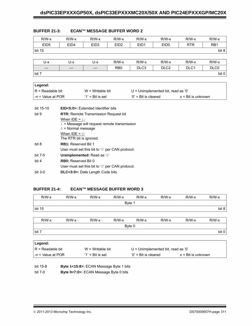
dsPIC33EPXXXGP50X, dsPIC33EPXXXMC20X/50X AND PIC24EPXXXGP/MC20X
(
BUFFER 21-3: ECAN™ MESSAGE BUFFER WORD 2
R/W-x R/W-x R/W-x R/W-x R/W-x R/W-x R/W-x R/W-x
EID5 EID4 EID3 EID2 EID1 EID0 RTR RB1
bit 15 bit 8
U-x U-x U-x R/W-x R/W-x R/W-x R/W-x R/W-x
— — — RB0 DLC3 DLC2 DLC1 DLC0
bit 7 bit 0
Legend:
R = Readable bit W = Writable bit U = Unimplemented bit, read as ‘0’
-n = Value at POR ‘1’ = Bit is set ‘0’ = Bit is cleared x = Bit is unknown
bit 15-10 EID<5:0>: Extended Identifier bits
bit 9 RTR: Remote Transmission Request bit
When IDE = 1:1 = Message will request remote transmission0 = Normal message
When IDE = 0:The RTR bit is ignored.
bit 8 RB1: Reserved Bit 1
User must set this bit to ‘0’ per CAN protocol.
bit 7-5 Unimplemented: Read as ‘0’
bit 4 RB0: Reserved Bit 0
User must set this bit to ‘0’ per CAN protocol.
bit 3-0 DLC<3:0>: Data Length Code bits
BUFFER 21-4: ECAN™ MESSAGE BUFFER WORD 3
R/W-x R/W-x R/W-x R/W-x R/W-x R/W-x R/W-x R/W-x
Byte 1
bit 15 bit 8
R/W-x R/W-x R/W-x R/W-x R/W-x R/W-x R/W-x R/W-x
Byte 0
bit 7 bit 0
Legend:
R = Readable bit W = Writable bit U = Unimplemented bit, read as ‘0’
-n = Value at POR ‘1’ = Bit is set ‘0’ = Bit is cleared x = Bit is unknown
bit 15-8 Byte 1<15:8>: ECAN Message Byte 1 bits
bit 7-0 Byte 0<7:0>: ECAN Message Byte 0 bits
2011-2013 Microchip Technology Inc. DS70000657H-page 311
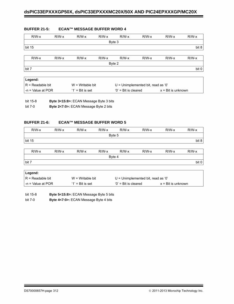
dsPIC33EPXXXGP50X, dsPIC33EPXXXMC20X/50X AND PIC24EPXXXGP/MC20X
BUFFER 21-5: ECAN™ MESSAGE BUFFER WORD 4
R/W-x R/W-x R/W-x R/W-x R/W-x R/W-x R/W-x R/W-x
Byte 3
bit 15 bit 8
R/W-x R/W-x R/W-x R/W-x R/W-x R/W-x R/W-x R/W-x
Byte 2
bit 7 bit 0
Legend:
R = Readable bit W = Writable bit U = Unimplemented bit, read as ‘0’
-n = Value at POR ‘1’ = Bit is set ‘0’ = Bit is cleared x = Bit is unknown
bit 15-8 Byte 3<15:8>: ECAN Message Byte 3 bits
bit 7-0 Byte 2<7:0>: ECAN Message Byte 2 bits
BUFFER 21-6: ECAN™ MESSAGE BUFFER WORD 5
R/W-x R/W-x R/W-x R/W-x R/W-x R/W-x R/W-x R/W-x
Byte 5
bit 15 bit 8
R/W-x R/W-x R/W-x R/W-x R/W-x R/W-x R/W-x R/W-x
Byte 4
bit 7 bit 0
Legend:
R = Readable bit W = Writable bit U = Unimplemented bit, read as ‘0’
-n = Value at POR ‘1’ = Bit is set ‘0’ = Bit is cleared x = Bit is unknown
bit 15-8 Byte 5<15:8>: ECAN Message Byte 5 bits
bit 7-0 Byte 4<7:0>: ECAN Message Byte 4 bits
DS70000657H-page 312 2011-2013 Microchip Technology Inc.

dsPIC33EPXXXGP50X, dsPIC33EPXXXMC20X/50X AND PIC24EPXXXGP/MC20X
BUFFER 21-7: ECAN™ MESSAGE BUFFER WORD 6
R/W-x R/W-x R/W-x R/W-x R/W-x R/W-x R/W-x R/W-x
Byte 7
bit 15 bit 8
R/W-x R/W-x R/W-x R/W-x R/W-x R/W-x R/W-x R/W-x
Byte 6
bit 7 bit 0
Legend:
R = Readable bit W = Writable bit U = Unimplemented bit, read as ‘0’
-n = Value at POR ‘1’ = Bit is set ‘0’ = Bit is cleared x = Bit is unknown
bit 15-8 Byte 7<15:8>: ECAN Message Byte 7 bits
bit 7-0 Byte 6<7:0>: ECAN Message Byte 6 bits
BUFFER 21-8: ECAN™ MESSAGE BUFFER WORD 7
U-0 U-0 U-0 R/W-x R/W-x R/W-x R/W-x R/W-x
— — — FILHIT4(1) FILHIT3(1) FILHIT2(1) FILHIT1(1) FILHIT0(1)
bit 15 bit 8
U-0 U-0 U-0 U-0 U-0 U-0 U-0 U-0
— — — — — — — —
bit 7 bit 0
Legend:
R = Readable bit W = Writable bit U = Unimplemented bit, read as ‘0’
-n = Value at POR ‘1’ = Bit is set ‘0’ = Bit is cleared x = Bit is unknown
bit 15-13 Unimplemented: Read as ‘0’
bit 12-8 FILHIT<4:0>: Filter Hit Code bits(1)
Encodes number of filter that resulted in writing this buffer.
bit 7-0 Unimplemented: Read as ‘0’
Note 1: Only written by module for receive buffers, unused for transmit buffers.
2011-2013 Microchip Technology Inc. DS70000657H-page 313

dsPIC33EPXXXGP50X, dsPIC33EPXXXMC20X/50X AND PIC24EPXXXGP/MC20X
NOTES:
DS70000657H-page 314 2011-2013 Microchip Technology Inc.
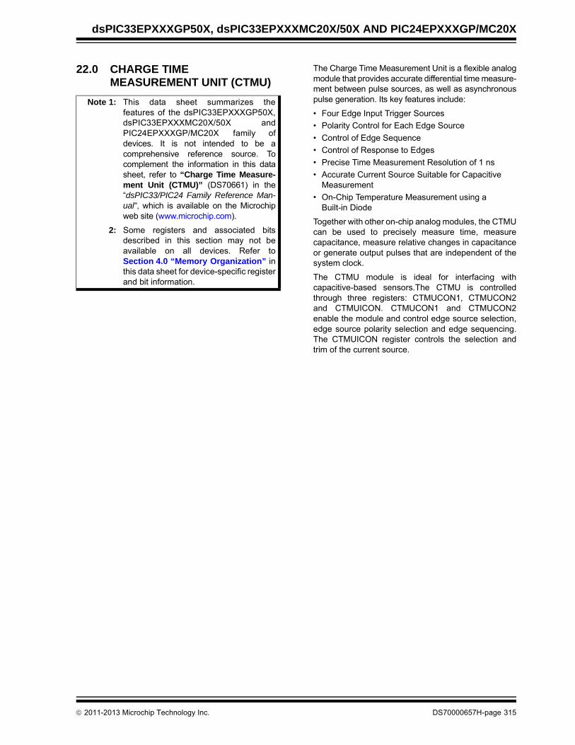
dsPIC33EPXXXGP50X, dsPIC33EPXXXMC20X/50X AND PIC24EPXXXGP/MC20X
22.0 CHARGE TIME MEASUREMENT UNIT (CTMU)
The Charge Time Measurement Unit is a flexible analogmodule that provides accurate differential time measure-ment between pulse sources, as well as asynchronouspulse generation. Its key features include:
• Four Edge Input Trigger Sources
• Polarity Control for Each Edge Source
• Control of Edge Sequence
• Control of Response to Edges
• Precise Time Measurement Resolution of 1 ns
• Accurate Current Source Suitable for Capacitive Measurement
• On-Chip Temperature Measurement using a Built-in Diode
Together with other on-chip analog modules, the CTMUcan be used to precisely measure time, measurecapacitance, measure relative changes in capacitanceor generate output pulses that are independent of thesystem clock.
The CTMU module is ideal for interfacing withcapacitive-based sensors.The CTMU is controlledthrough three registers: CTMUCON1, CTMUCON2and CTMUICON. CTMUCON1 and CTMUCON2enable the module and control edge source selection,edge source polarity selection and edge sequencing.The CTMUICON register controls the selection andtrim of the current source.
Note 1: This data sheet summarizes thefeatures of the dsPIC33EPXXXGP50X,dsPIC33EPXXXMC20X/50X andPIC24EPXXXGP/MC20X family ofdevices. It is not intended to be acomprehensive reference source. Tocomplement the information in this datasheet, refer to “Charge Time Measure-ment Unit (CTMU)” (DS70661) in the“dsPIC33/PIC24 Family Reference Man-ual”, which is available on the Microchipweb site (www.microchip.com).
2: Some registers and associated bitsdescribed in this section may not beavailable on all devices. Refer toSection 4.0 “Memory Organization” inthis data sheet for device-specific registerand bit information.
2011-2013 Microchip Technology Inc. DS70000657H-page 315

dsPIC33EPXXXGP50X, dsPIC33EPXXXMC20X/50X AND PIC24EPXXXGP/MC20X
FIGURE 22-1: CTMU BLOCK DIAGRAM
22.1 CTMU Resources
Many useful resources are provided on the main prod-uct page of the Microchip web site for the devices listedin this data sheet. This product page, which can beaccessed using this link, contains the latest updatesand additional information.
22.1.1 KEY RESOURCES
• “Charge Time Measurement Unit (CTMU)” (DS70661) in the “dsPIC33/PIC24 Family Reference Manual”
• Code Samples
• Application Notes
• Software Libraries
• Webinars
• All Related “dsPIC33/PIC24 Family Reference Manual” Sections
• Development Tools
CTED1
CTED2
Current Source
EdgeControlLogic
PulseGenerator
CMP1
Timer1OC1
CurrentControl
ITRIM<5:0>IRNG<1:0>
CTMUControlLogic
EDG1STATEDG2STAT
Analog-to-Digital
CTPLSIC1CMP1
C1IN1-
CDelay
CTMU TEMP(3)
CTMUTemperature
Sensor
Current Control Selection TGEN EDG1STAT, EDG2STAT
CTMU TEMP 0 EDG1STAT = EDG2STAT
CTMUI to ADC(2) 0 EDG1STAT EDG2STAT
CTMUP 1 EDG1STAT EDG2STAT
Internal Current Flow(4) 1 EDG1STAT = EDG2STAT
TriggerTGEN
CTMUP
External Capacitorfor Pulse Generation
CTMUI to ADC(2)
Note 1: When the CTMU is not actively used, set TGEN = 1, and ensure that EDG1STAT = EDG2STAT. All other settings allow current to flow into the ADC or the C1IN1- pin. If using the ADC for other purposes besides the CTMU, set IDISSEN = 0. If IDISSEN is set to ‘1’, it will short the output of the ADC CH0 MUX to VSS.
2: CTMUI connects to the output of the ADC CH0 MUX. When CTMU current is steered into this node, the current will flow out through the selected ADC channel determined by the CH0 MUX (see the CH0Sx bits in the AD1CHS0 register).
3: CTMU TEMP connects to one of the ADC CH0 inputs; see CH0SA and CH0SB (AD1CHS0<12:8,4:0).4: If TGEN = 1 and EDG1STAT = EDG2STAT, CTMU current source is still enabled and may be shunted to VSS internally. This
should be considered in low-power applications.5: The switch connected to ADC CH0 is closed when IDISSEN (CTMUCON1<9>) = 1, and opened when IDISSEN = 0.
ADCCH0(5)
CTMUCON1 or CTMUCON2(1)
CTMUICON
Note: In the event you are not able to access theproduct page using the link above, enterthis URL in your browser:http://www.microchip.com/wwwproducts/Devices.aspx?dDocName=en555464
DS70000657H-page 316 2011-2013 Microchip Technology Inc.

dsPIC33EPXXXGP50X, dsPIC33EPXXXMC20X/50X AND PIC24EPXXXGP/MC20X
22.2 CTMU Control Registers
REGISTER 22-1: CTMUCON1: CTMU CONTROL REGISTER 1
R/W-0 U-0 R/W-0 R/W-0 R/W-0 R/W-0 R/W-0 R/W-0
CTMUEN — CTMUSIDL TGEN EDGEN EDGSEQEN IDISSEN(1) CTTRIG
bit 15 bit 8
U-0 U-0 U-0 U-0 U-0 U-0 U-0 U-0
— — — — — — — —
bit 7 bit 0
Legend:
R = Readable bit W = Writable bit U = Unimplemented bit, read as ‘0’
-n = Value at POR ‘1’ = Bit is set ‘0’ = Bit is cleared x = Bit is unknown
bit 15 CTMUEN: CTMU Enable bit
1 = Module is enabled0 = Module is disabled
bit 14 Unimplemented: Read as ‘0’
bit 13 CTMUSIDL: CTMU Stop in Idle Mode bit
1 = Discontinues module operation when device enters Idle mode0 = Continues module operation in Idle mode
bit 12 TGEN: Time Generation Enable bit
1 = Enables edge delay generation0 = Disables edge delay generation
bit 11 EDGEN: Edge Enable bit
1 = Hardware modules are used to trigger edges (TMRx, CTEDx, etc.)0 = Software is used to trigger edges (manual set of EDGxSTAT)
bit 10 EDGSEQEN: Edge Sequence Enable bit
1 = Edge 1 event must occur before Edge 2 event can occur0 = No edge sequence is needed
bit 9 IDISSEN: Analog Current Source Control bit(1)
1 = Analog current source output is grounded0 = Analog current source output is not grounded
bit 8 CTTRIG: ADC Trigger Control bit
1 = CTMU triggers ADC start of conversion0 = CTMU does not trigger ADC start of conversion
bit 7-0 Unimplemented: Read as ‘0’
Note 1: The ADC module Sample-and-Hold capacitor is not automatically discharged between sample/conversion cycles. Software using the ADC as part of a capacitance measurement must discharge the ADC capacitor before conducting the measurement. The IDISSEN bit, when set to ‘1’, performs this function. The ADC must be sampling while the IDISSEN bit is active to connect the discharge sink to the capacitor array.
2011-2013 Microchip Technology Inc. DS70000657H-page 317
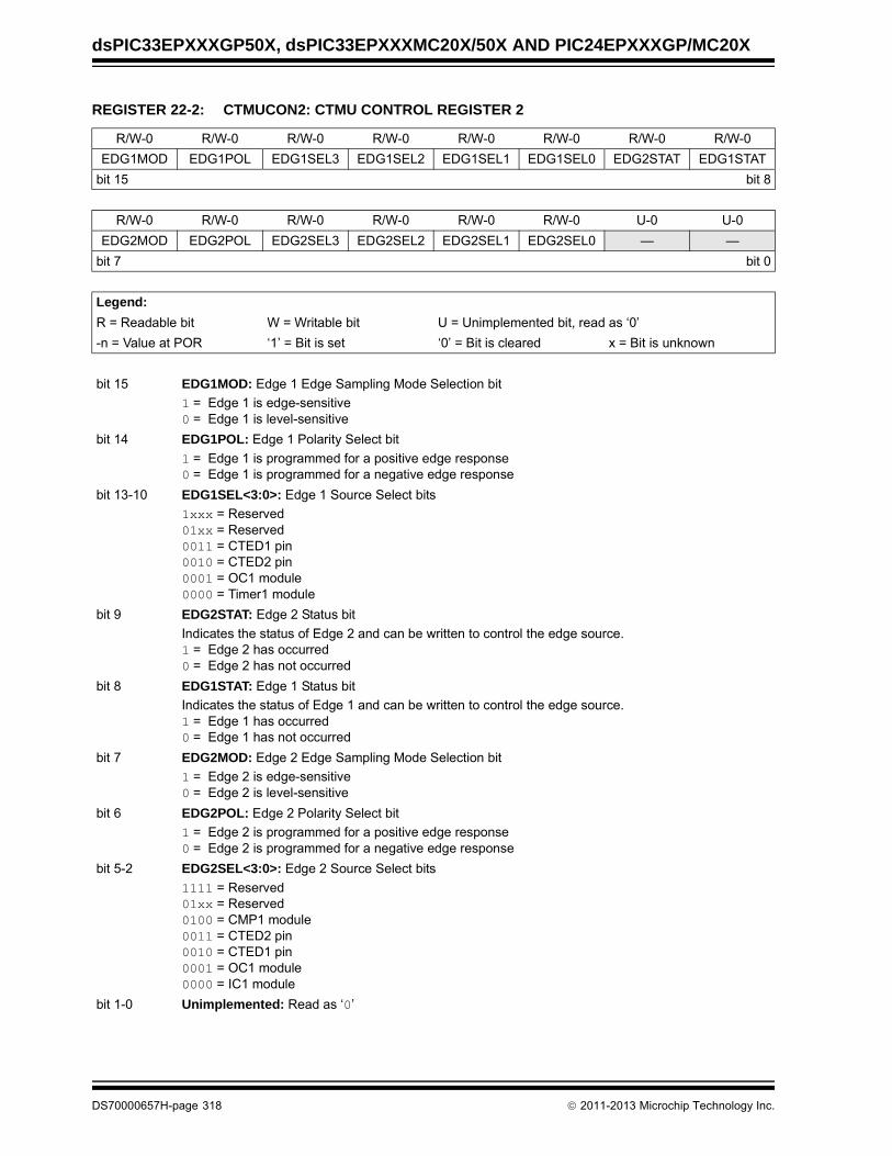
dsPIC33EPXXXGP50X, dsPIC33EPXXXMC20X/50X AND PIC24EPXXXGP/MC20X
REGISTER 22-2: CTMUCON2: CTMU CONTROL REGISTER 2
R/W-0 R/W-0 R/W-0 R/W-0 R/W-0 R/W-0 R/W-0 R/W-0
EDG1MOD EDG1POL EDG1SEL3 EDG1SEL2 EDG1SEL1 EDG1SEL0 EDG2STAT EDG1STAT
bit 15 bit 8
R/W-0 R/W-0 R/W-0 R/W-0 R/W-0 R/W-0 U-0 U-0
EDG2MOD EDG2POL EDG2SEL3 EDG2SEL2 EDG2SEL1 EDG2SEL0 — —
bit 7 bit 0
Legend:
R = Readable bit W = Writable bit U = Unimplemented bit, read as ‘0’
-n = Value at POR ‘1’ = Bit is set ‘0’ = Bit is cleared x = Bit is unknown
bit 15 EDG1MOD: Edge 1 Edge Sampling Mode Selection bit
1 = Edge 1 is edge-sensitive0 = Edge 1 is level-sensitive
bit 14 EDG1POL: Edge 1 Polarity Select bit
1 = Edge 1 is programmed for a positive edge response0 = Edge 1 is programmed for a negative edge response
bit 13-10 EDG1SEL<3:0>: Edge 1 Source Select bits
1xxx = Reserved01xx = Reserved0011 = CTED1 pin0010 = CTED2 pin0001 = OC1 module0000 = Timer1 module
bit 9 EDG2STAT: Edge 2 Status bit
Indicates the status of Edge 2 and can be written to control the edge source.1 = Edge 2 has occurred0 = Edge 2 has not occurred
bit 8 EDG1STAT: Edge 1 Status bit
Indicates the status of Edge 1 and can be written to control the edge source.1 = Edge 1 has occurred0 = Edge 1 has not occurred
bit 7 EDG2MOD: Edge 2 Edge Sampling Mode Selection bit
1 = Edge 2 is edge-sensitive0 = Edge 2 is level-sensitive
bit 6 EDG2POL: Edge 2 Polarity Select bit
1 = Edge 2 is programmed for a positive edge response0 = Edge 2 is programmed for a negative edge response
bit 5-2 EDG2SEL<3:0>: Edge 2 Source Select bits
1111 = Reserved01xx = Reserved0100 = CMP1 module0011 = CTED2 pin0010 = CTED1 pin0001 = OC1 module0000 = IC1 module
bit 1-0 Unimplemented: Read as ‘0’
DS70000657H-page 318 2011-2013 Microchip Technology Inc.

dsPIC33EPXXXGP50X, dsPIC33EPXXXMC20X/50X AND PIC24EPXXXGP/MC20X
REGISTER 22-3: CTMUICON: CTMU CURRENT CONTROL REGISTER
R/W-0 R/W-0 R/W-0 R/W-0 R/W-0 R/W-0 R/W-0 R/W-0
ITRIM5 ITRIM4 ITRIM3 ITRIM2 ITRIM1 ITRIM0 IRNG1 IRNG0
bit 15 bit 8
U-0 U-0 U-0 U-0 U-0 U-0 U-0 U-0
— — — — — — — —
bit 7 bit 0
Legend:
R = Readable bit W = Writable bit U = Unimplemented bit, read as ‘0’
-n = Value at POR ‘1’ = Bit is set ‘0’ = Bit is cleared x = Bit is unknown
bit 15-10 ITRIM<5:0>: Current Source Trim bits
011111 = Maximum positive change from nominal current + 62%011110 = Maximum positive change from nominal current + 60%
•
•
•
000010 = Minimum positive change from nominal current + 4%000001 = Minimum positive change from nominal current + 2%000000 = Nominal current output specified by IRNG<1:0>111111 = Minimum negative change from nominal current – 2%111110 = Minimum negative change from nominal current – 4%
•
•
•
100010 = Maximum negative change from nominal current – 60%100001 = Maximum negative change from nominal current – 62%
bit 9-8 IRNG<1:0>: Current Source Range Select bits
11 = 100 Base Current(2)
10 = 10 Base Current(2)
01 = Base Current Level(2)
00 = 1000 Base Current(1,2)
bit 7-0 Unimplemented: Read as ‘0’
Note 1: This current range is not available to be used with the internal temperature measurement diode.
2: Refer to the CTMU Current Source Specifications (Table 30-56) in Section 30.0 “Electrical Characteristics” for the current range selection values.
2011-2013 Microchip Technology Inc. DS70000657H-page 319

dsPIC33EPXXXGP50X, dsPIC33EPXXXMC20X/50X AND PIC24EPXXXGP/MC20X
NOTES:
DS70000657H-page 320 2011-2013 Microchip Technology Inc.

dsPIC33EPXXXGP50X, dsPIC33EPXXXMC20X/50X AND PIC24EPXXXGP/MC20X
23.0 10-BIT/12-BIT ANALOG-TO-DIGITAL CONVERTER (ADC)
The dsPIC33EPXXXGP50X, dsPIC33EPXXXMC20X/50X and PIC24EPXXXGP/MC20X devices have oneADC module. The ADC module supports up to16 analog input channels.
On ADC1, the AD12B bit (AD1CON1<10>) allows theADC module to be configured by the user as either a10-bit, 4 Sample-and-Hold (S&H) ADC (defaultconfiguration) or a 12-bit, 1 S&H ADC.
23.1 Key Features
23.1.1 10-BIT ADC CONFIGURATION
The 10-bit ADC configuration has the following keyfeatures:
• Successive Approximation (SAR) conversion
• Conversion speeds of up to 1.1 Msps
• Up to 16 analog input pins
• Connections to three internal op amps
• Connections to the Charge Time Measurement Unit (CTMU) and temperature measurement diode
• Channel selection and triggering can be controlled by the Peripheral Trigger Generator (PTG)
• External voltage reference input pins
• Simultaneous sampling of:
- Up to four analog input pins
- Three op amp outputs
- Combinations of analog inputs and op amp outputs
• Automatic Channel Scan mode
• Selectable conversion Trigger source
• Selectable Buffer Fill modes
• Four result alignment options (signed/unsigned, fractional/integer)
• Operation during CPU Sleep and Idle modes
23.1.2 12-BIT ADC CONFIGURATION
The 12-bit ADC configuration supports all the featureslisted above, with the exception of the following:
• In the 12-bit configuration, conversion speeds of up to 500 ksps are supported
• There is only one S&H amplifier in the 12-bit configuration; therefore, simultaneous sampling of multiple channels is not supported.
Depending on the particular device pinout, the ADCcan have up to 16 analog input pins, designated AN0through AN15. These analog inputs are shared withop amp inputs and outputs, comparator inputs, andexternal voltage references. When op amp/comparatorfunctionality is enabled, or an external voltage refer-ence is used, the analog input that shares that pin is nolonger available. The actual number of analog inputpins, op amps and external voltage reference inputconfiguration depends on the specific device.
A block diagram of the ADC module is shown inFigure 23-1. Figure 23-2 provides a diagram of theADC conversion clock period.
Note 1: This data sheet summarizes thefeatures of the dsPIC33EPXXXGP50X,dsPIC33EPXXXMC20X/50X andPIC24EPXXXGP/MC20X families ofdevices. It is not intended to be acomprehensive reference source. Tocomplement the information in this datasheet, refer to “Analog-to-DigitalConverter (ADC)” (DS70621) in the“dsPIC33/PIC24 Family ReferenceManual”, which is available from theMicrochip web site (www.microchip.com).
2: Some registers and associated bitsdescribed in this section may not beavailable on all devices. Refer toSection 4.0 “Memory Organization” inthis data sheet for device-specific registerand bit information.
Note: The ADC module needs to be disabledbefore modifying the AD12B bit.
2011-2013 Microchip Technology Inc. DS70000657H-page 321

ds
PIC
33E
PX
XX
GP
50X
, dsP
IC33
EP
XX
XM
C20
X/5
0X A
ND
PIC
24E
PX
XX
GP
/MC
20X
DS
70
00
06
57
H-p
ag
e 3
22
2
01
1-2
01
3 M
icroch
ip T
ech
no
log
y Inc.
D OP AMPS
A
B
1
0CH0SA<4:0>(3)
CH0SB<4:0>(3)CH0Sx
CH0NxCH0NA(3)
CH0NB(3)
CSCNA
CH123Sx
CH123Nx
CH123SA
CH123SB
CH123NA<2:0>
CH123NB<2:0>
Alternate Input
Selection
annel Scan
A
B
A
B
A
B
EF+(1) AVDD AVSSVREF-(1)
VCFG<2:0> ADC1BUF0(4)
ADC1BUF1(4)
ADC1BUF2(4)
ADC1BUFF(4)ADC1BUFE(4)
e” for more information.
ALTS (MUXA/MUXB)
SAR ADC
VREFH VREFL
FIGURE 23-1: ADC MODULE BLOCK DIAGRAM WITH CONNECTION OPTIONS FOR ANx PINS AN
0
1
+
–
CMP1/OA1
0x
10
11
VREFL
VREFL
VREFL
+
–CH0
0
1
VREFL
AN0-ANxOA1-OA3
CH0Sx
CH0Nx
CH123Nx
00000
11111
OPMODE
OPMODE
OPMODE
S&H1
Ch
This diagram depicts all of the availableADC connection options to the four S&Hamplifiers, which are designated: CH0,CH1, CH2 and CH3.
The ANx analog pins or op amp outputsare connected to the CH0-CH3 amplifi-ers through the multiplexers, controlledby the SFR control bits, CH0Sx,CHONx, CH123Sx and CH123Nx.
+
–CH1
+
–CH2
+
–CH3
0
1
CH123Sx
+
–OA2
0
1
CH123Sx
0x
10
11
CH123Nx
0x
10
11
CH123Nx
+
–OA3(5)
CH123Sx
AN0/OA2OUT/RA0
PGEC1/AN4/C1IN1+/RPI34/RB2
PGED1/AN5/C1IN1-/RP35/RB3
PGEC3/VREF+/AN3/OA1OUT/RPI33/CTED1/RB1
AN9/RPI27/RA11
AN1/C2IN1+/RA1
AN10/RPI28/RA12
PGED3/VREF-/AN2/C2IN1-/SS1/RPI32/CTED2/RB0
AN8/C3IN1+/U1RTS/BCLK1/RC2
AN6/OA3OUT/C4IN1+/OCFB/RC0
AN7/C3IN1-/C4IN1-/RC1
AN11/C1IN2-/U1CTS/RC11
+
–OA1
VR
From CTMUCurrent Source (CTMUI)CTMU Temp
S&H2
S&H3
S&H0
Note 1: VREF+, VREF- inputs can be multiplexed with other analog inputs.2: Channels 1, 2 and 3 are not applicable for the 12-bit mode of operation.3: These bits can be updated with Step commands from the PTG module. See Section 24.0 “Peripheral Trigger Generator (PTG) Modul4: When ADDMAEN (AD1CON4<8>) = 1, enabling DMA, only ADC1BUF0 is used.5: OA3 is not available for 28-pin devices.
Open

dsPIC33EPXXXGP50X, dsPIC33EPXXXMC20X/50X AND PIC24EPXXXGP/MC20X
FIGURE 23-2: ADC CONVERSION CLOCK PERIOD BLOCK DIAGRAM
1
0
ADC ConversionClock Multiplier
1, 2, 3, 4, 5,..., 256
AD1CON3<15>
TP(1)
TAD
6
AD1CON3<7:0>
Note 1: TP = 1/FP.
2: See the ADC electrical specifications in Section 30.0 “Electrical Characteristics” for the exact RC clock value.
ADC InternalRC Clock(2)
2011-2013 Microchip Technology Inc. DS70000657H-page 323

dsPIC33EPXXXGP50X, dsPIC33EPXXXMC20X/50X AND PIC24EPXXXGP/MC20X
23.2 ADC Helpful Tips
1. The SMPIx control bits in the AD1CON2 register:
a) Determine when the ADC interrupt flag isset and an interrupt is generated, ifenabled.
b) When the CSCNA bit in the AD1CON2 reg-isters is set to ‘1’, this determines when theADC analog scan channel list, defined inthe AD1CSSL/AD1CSSH registers, startsover from the beginning.
c) When the DMA peripheral is not used(ADDMAEN = 0), this determines when theADC Result Buffer Pointer to ADC1BUF0-ADC1BUFF gets reset back to thebeginning at ADC1BUF0.
d) When the DMA peripheral is used(ADDMAEN = 1), this determines when theDMA Address Pointer is incremented after asample/conversion operation. ADC1BUF0 isthe only ADC buffer used in this mode. TheADC Result Buffer Pointer to ADC1BUF0-ADC1BUFF gets reset back to the beginningat ADC1BUF0. The DMA address isincremented after completion of every 32ndsample/conversion operation. Conversionresults are stored in the ADC1BUF0 registerfor transfer to RAM using DMA.
2. When the DMA module is disabled(ADDMAEN = 0), the ADC has 16 result buffers.ADC conversion results are stored sequentiallyin ADC1BUF0-ADC1BUFF, regardless of whichanalog inputs are being used subject to theSMPIx bits and the condition described in 1c)above. There is no relationship between theANx input being measured and which ADCbuffer (ADC1BUF0-ADC1BUFF) that theconversion results will be placed in.
3. When the DMA module is enabled(ADDMAEN = 1), the ADC module has only1 ADC result buffer (i.e., ADC1BUF0) per ADCperipheral and the ADC conversion result mustbe read, either by the CPU or DMA Controller,before the next ADC conversion is complete toavoid overwriting the previous value.
4. The DONE bit (AD1CON1<0>) is only cleared atthe start of each conversion and is set at thecompletion of the conversion, but remains setindefinitely, even through the next sample phaseuntil the next conversion begins. If applicationcode is monitoring the DONE bit in any kind ofsoftware loop, the user must consider this behav-ior because the CPU code execution is fasterthan the ADC. As a result, in Manual Samplemode, particularly where the user’s code is set-ting the SAMP bit (AD1CON1<1>), the DONE bitshould also be cleared by the user applicationjust before setting the SAMP bit.
5. Enabling op amps, comparator inputs and exter-nal voltage references can limit the availability ofanalog inputs (ANx pins). For example, when OpAmp 2 is enabled, the pins for AN0, AN1 and AN2are used by the op amp’s inputs and output. Thisnegates the usefulness of Alternate Input modesince the MUXA selections use AN0-AN2.Carefully study the ADC block diagram to deter-mine the configuration that will best suit yourapplication. Configuration examples are avail-able in the “Analog-to-Digital Converter(ADC)” (DS70621) section in the “dsPIC33/PIC24 Family Reference Manual”.
23.3 ADC Resources
Many useful resources are provided on the main prod-uct page of the Microchip web site for the devices listedin this data sheet. This product page, which can beaccessed using this link, contains the latest updatesand additional information.
23.3.1 KEY RESOURCES
• “Analog-to-Digital Converter (ADC)” (DS70621) in the “dsPIC33/PIC24 Family Reference Manual”
• Code Samples
• Application Notes
• Software Libraries
• Webinars
• All Related “dsPIC33/PIC24 Family Reference Manual” Sections
• Development Tools
Note: In the event you are not able to access theproduct page using the link above, enterthis URL in your browser:http://www.microchip.com/wwwproducts/Devices.aspx?dDocName=en555464
DS70000657H-page 324 2011-2013 Microchip Technology Inc.

dsPIC33EPXXXGP50X, dsPIC33EPXXXMC20X/50X AND PIC24EPXXXGP/MC20X
23.4 ADC Control Registers
REGISTER 23-1: AD1CON1: ADC1 CONTROL REGISTER 1
R/W-0 U-0 R/W-0 R/W-0 U-0 R/W-0 R/W-0 R/W-0
ADON — ADSIDL ADDMABM — AD12B FORM1 FORM0
bit 15 bit 8
R/W-0 R/W-0 R/W-0 R/W-0 R/W-0 R/W-0 R/W-0, HC, HS R/C-0, HC, HS
SSRC2 SSRC1 SSRC0 SSRCG SIMSAM ASAM SAMP DONE(3)
bit 7 bit 0
Legend: HC = Hardware Clearable bit HS = Hardware Settable bit C = Clearable bit
R = Readable bit W = Writable bit U = Unimplemented bit, read as ‘0’
-n = Value at POR ‘1’ = Bit is set ‘0’ = Bit is cleared x = Bit is unknown
bit 15 ADON: ADC1 Operating Mode bit
1 = ADC module is operating0 = ADC is off
bit 14 Unimplemented: Read as ‘0’
bit 13 ADSIDL: ADC1 Stop in Idle Mode bit
1 = Discontinues module operation when device enters Idle mode0 = Continues module operation in Idle mode
bit 12 ADDMABM: DMA Buffer Build Mode bit
1 = DMA buffers are written in the order of conversion; the module provides an address to the DMAchannel that is the same as the address used for the non-DMA stand-alone buffer
0 = DMA buffers are written in Scatter/Gather mode; the module provides a Scatter/Gather address tothe DMA channel, based on the index of the analog input and the size of the DMA buffer.
bit 11 Unimplemented: Read as ‘0’
bit 10 AD12B: ADC1 10-Bit or 12-Bit Operation Mode bit
1 = 12-bit, 1-channel ADC operation0 = 10-bit, 4-channel ADC operation
bit 9-8 FORM<1:0>: Data Output Format bits
For 10-Bit Operation:11 = Signed fractional (DOUT = sddd dddd dd00 0000, where s = .NOT.d<9>)10 = Fractional (DOUT = dddd dddd dd00 0000)01 = Signed integer (DOUT = ssss sssd dddd dddd, where s = .NOT.d<9>)00 = Integer (DOUT = 0000 00dd dddd dddd)
For 12-Bit Operation:11 = Signed fractional (DOUT = sddd dddd dddd 0000, where s = .NOT.d<11>)10 = Fractional (DOUT = dddd dddd dddd 0000)01 = Signed integer (DOUT = ssss sddd dddd dddd, where s = .NOT.d<11>)00 = Integer (DOUT = 0000 dddd dddd dddd)
Note 1: See Section 24.0 “Peripheral Trigger Generator (PTG) Module” for information on this selection.
2: This setting is available in dsPIC33EPXXXMC20X/50X and PIC24EPXXXMC20X devices only.
3: Do not clear the DONE bit in software if Auto-Sample is enabled (ASAM = 1).
2011-2013 Microchip Technology Inc. DS70000657H-page 325

dsPIC33EPXXXGP50X, dsPIC33EPXXXMC20X/50X AND PIC24EPXXXGP/MC20X
bit 7-5 SSRC<2:0>: Sample Trigger Source Select bits
If SSRCG = 1:111 = Reserved110 = PTGO15 primary trigger compare ends sampling and starts conversion(1)
101 = PTGO14 primary trigger compare ends sampling and starts conversion(1)
100 = PTGO13 primary trigger compare ends sampling and starts conversion(1)
011 = PTGO12 primary trigger compare ends sampling and starts conversion(1)
010 = PWM Generator 3 primary trigger compare ends sampling and starts conversion(2)
001 = PWM Generator 2 primary trigger compare ends sampling and starts conversion(2)
000 = PWM Generator 1 primary trigger compare ends sampling and starts conversion(2)
If SSRCG = 0:111 = Internal counter ends sampling and starts conversion (auto-convert)110 = CTMU ends sampling and starts conversion101 = Reserved100 = Timer5 compare ends sampling and starts conversion011 = PWM primary Special Event Trigger ends sampling and starts conversion(2)
010 = Timer3 compare ends sampling and starts conversion001 = Active transition on the INT0 pin ends sampling and starts conversion000 = Clearing the Sample bit (SAMP) ends sampling and starts conversion (Manual mode)
bit 4 SSRCG: Sample Trigger Source Group bit
See SSRC<2:0> for details.
bit 3 SIMSAM: Simultaneous Sample Select bit (only applicable when CHPS<1:0> = 01 or 1x)
In 12-bit mode (AD21B = 1), SIMSAM is Unimplemented and is Read as ‘0’:1 = Samples CH0, CH1, CH2, CH3 simultaneously (when CHPS<1:0> = 1x); or samples CH0 and CH1
simultaneously (when CHPS<1:0> = 01)0 = Samples multiple channels individually in sequence
bit 2 ASAM: ADC1 Sample Auto-Start bit
1 = Sampling begins immediately after the last conversion; SAMP bit is auto-set0 = Sampling begins when the SAMP bit is set
bit 1 SAMP: ADC1 Sample Enable bit
1 = ADC Sample-and-Hold amplifiers are sampling0 = ADC Sample-and-Hold amplifiers are holdingIf ASAM = 0, software can write ‘1’ to begin sampling. Automatically set by hardware if ASAM = 1. IfSSRC<2:0> = 000, software can write ‘0’ to end sampling and start conversion. If SSRC<2:0> 000,automatically cleared by hardware to end sampling and start conversion.
bit 0 DONE: ADC1 Conversion Status bit(3)
1 = ADC conversion cycle has completed0 = ADC conversion has not started or is in progressAutomatically set by hardware when the ADC conversion is complete. Software can write ‘0’ to clear the DONE status bit (software is not allowed to write ‘1’). Clearing this bit does NOT affect any operation in progress. Automatically cleared by hardware at the start of a new conversion.
REGISTER 23-1: AD1CON1: ADC1 CONTROL REGISTER 1 (CONTINUED)
Note 1: See Section 24.0 “Peripheral Trigger Generator (PTG) Module” for information on this selection.
2: This setting is available in dsPIC33EPXXXMC20X/50X and PIC24EPXXXMC20X devices only.
3: Do not clear the DONE bit in software if Auto-Sample is enabled (ASAM = 1).
DS70000657H-page 326 2011-2013 Microchip Technology Inc.
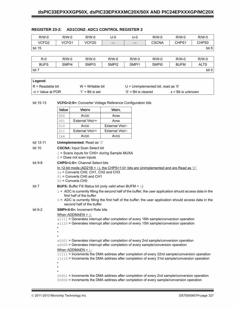
dsPIC33EPXXXGP50X, dsPIC33EPXXXMC20X/50X AND PIC24EPXXXGP/MC20X
REGISTER 23-2: AD1CON2: ADC1 CONTROL REGISTER 2
R/W-0 R/W-0 R/W-0 U-0 U-0 R/W-0 R/W-0 R/W-0
VCFG2 VCFG1 VCFG0 — — CSCNA CHPS1 CHPS0
bit 15 bit 8
R-0 R/W-0 R/W-0 R/W-0 R/W-0 R/W-0 R/W-0 R/W-0
BUFS SMPI4 SMPI3 SMPI2 SMPI1 SMPI0 BUFM ALTS
bit 7 bit 0
Legend:
R = Readable bit W = Writable bit U = Unimplemented bit, read as ‘0’
-n = Value at POR ‘1’ = Bit is set ‘0’ = Bit is cleared x = Bit is unknown
bit 15-13 VCFG<2:0>: Converter Voltage Reference Configuration bits
bit 12-11 Unimplemented: Read as ‘0’
bit 10 CSCNA: Input Scan Select bit
1 = Scans inputs for CH0+ during Sample MUXA0 = Does not scan inputs
bit 9-8 CHPS<1:0>: Channel Select bits
In 12-bit mode (AD21B = 1), the CHPS<1:0> bits are Unimplemented and are Read as ‘0’:1x = Converts CH0, CH1, CH2 and CH301 = Converts CH0 and CH100 = Converts CH0
bit 7 BUFS: Buffer Fill Status bit (only valid when BUFM = 1)
1 = ADC is currently filling the second half of the buffer; the user application should access data in thefirst half of the buffer
0 = ADC is currently filling the first half of the buffer; the user application should access data in thesecond half of the buffer
bit 6-2 SMPI<4:0>: Increment Rate bits
When ADDMAEN = 0:x1111 = Generates interrupt after completion of every 16th sample/conversion operationx1110 = Generates interrupt after completion of every 15th sample/conversion operation•••x0001 = Generates interrupt after completion of every 2nd sample/conversion operationx0000 = Generates interrupt after completion of every sample/conversion operation
When ADDMAEN = 1:11111 = Increments the DMA address after completion of every 32nd sample/conversion operation11110 = Increments the DMA address after completion of every 31st sample/conversion operation•••00001 = Increments the DMA address after completion of every 2nd sample/conversion operation00000 = Increments the DMA address after completion of every sample/conversion operation
Value VREFH VREFL
000 AVDD Avss
001 External VREF+ Avss
010 AVDD External VREF-
011 External VREF+ External VREF-
1xx AVDD AVSS
2011-2013 Microchip Technology Inc. DS70000657H-page 327

dsPIC33EPXXXGP50X, dsPIC33EPXXXMC20X/50X AND PIC24EPXXXGP/MC20X
bit 1 BUFM: Buffer Fill Mode Select bit
1 = Starts the buffer filling the first half of the buffer on the first interrupt and the second half of thebuffer on next interrupt
0 = Always starts filling the buffer from the start address.
bit 0 ALTS: Alternate Input Sample Mode Select bit
1 = Uses channel input selects for Sample MUXA on first sample and Sample MUXB on next sample0 = Always uses channel input selects for Sample MUXA
REGISTER 23-2: AD1CON2: ADC1 CONTROL REGISTER 2 (CONTINUED)
DS70000657H-page 328 2011-2013 Microchip Technology Inc.

dsPIC33EPXXXGP50X, dsPIC33EPXXXMC20X/50X AND PIC24EPXXXGP/MC20X
REGISTER 23-3: AD1CON3: ADC1 CONTROL REGISTER 3
R/W-0 U-0 U-0 R/W-0 R/W-0 R/W-0 R/W-0 R/W-0
ADRC — — SAMC4(1) SAMC3(1) SAMC2(1) SAMC1(1) SAMC0(1)
bit 15 bit 8
R/W-0 R/W-0 R/W-0 R/W-0 R/W-0 R/W-0 R/W-0 R/W-0
ADCS7(2) ADCS6(2) ADCS5(2) ADCS4(2) ADCS3(2) ADCS2(2) ADCS1(2) ADCS0(2)
bit 7 bit 0
Legend:
R = Readable bit W = Writable bit U = Unimplemented bit, read as ‘0’
-n = Value at POR ‘1’ = Bit is set ‘0’ = Bit is cleared x = Bit is unknown
bit 15 ADRC: ADC1 Conversion Clock Source bit
1 = ADC internal RC clock0 = Clock derived from system clock
bit 14-13 Unimplemented: Read as ‘0’
bit 12-8 SAMC<4:0>: Auto-Sample Time bits(1)
11111 = 31 TAD
•••00001 = 1 TAD
00000 = 0 TAD
bit 7-0 ADCS<7:0>: ADC1 Conversion Clock Select bits(2)
11111111 = TP • (ADCS<7:0> + 1) = TP •256 = TAD
•••00000010 = TP • (ADCS<7:0> + 1) = TP •3 = TAD 00000001 = TP • (ADCS<7:0> + 1) = TP •2 = TAD
00000000 = TP • (ADCS<7:0> + 1) = TP •1 = TAD
Note 1: This bit is only used if SSRC<2:0> (AD1CON1<7:5>) = 111 and SSRCG (AD1CON1<4>) = 0.
2: This bit is not used if ADRC (AD1CON3<15>) = 1.
2011-2013 Microchip Technology Inc. DS70000657H-page 329

dsPIC33EPXXXGP50X, dsPIC33EPXXXMC20X/50X AND PIC24EPXXXGP/MC20X
REGISTER 23-4: AD1CON4: ADC1 CONTROL REGISTER 4
U-0 U-0 U-0 U-0 U-0 U-0 U-0 R/W-0
— — — — — — — ADDMAEN
bit 15 bit 8
U-0 U-0 U-0 U-0 U-0 R/W-0 R/W-0 R/W-0
— — — — — DMABL2 DMABL1 DMABL0
bit 7 bit 0
Legend:
R = Readable bit W = Writable bit U = Unimplemented bit, read as ‘0’
-n = Value at POR ‘1’ = Bit is set ‘0’ = Bit is cleared x = Bit is unknown
bit 15-9 Unimplemented: Read as ‘0’
bit 8 ADDMAEN: ADC1 DMA Enable bit
1 = Conversion results are stored in the ADC1BUF0 register for transfer to RAM using DMA0 = Conversion results are stored in ADC1BUF0 through ADC1BUFF registers; DMA will not be used
bit 7-3 Unimplemented: Read as ‘0’
bit 2-0 DMABL<2:0>: Selects Number of DMA Buffer Locations per Analog Input bits
111 = Allocates 128 words of buffer to each analog input110 = Allocates 64 words of buffer to each analog input101 = Allocates 32 words of buffer to each analog input100 = Allocates 16 words of buffer to each analog input011 = Allocates 8 words of buffer to each analog input010 = Allocates 4 words of buffer to each analog input001 = Allocates 2 words of buffer to each analog input000 = Allocates 1 word of buffer to each analog input
DS70000657H-page 330 2011-2013 Microchip Technology Inc.

dsPIC33EPXXXGP50X, dsPIC33EPXXXMC20X/50X AND PIC24EPXXXGP/MC20X
REGISTER 23-5: AD1CHS123: ADC1 INPUT CHANNEL 1, 2, 3 SELECT REGISTER
U-0 U-0 U-0 U-0 U-0 R/W-0 R/W-0 R/W-0
— — — — — CH123NB1 CH123NB0 CH123SB
bit 15 bit 8
U-0 U-0 U-0 U-0 U-0 R/W-0 R/W-0 R/W-0
— — — — — CH123NA1 CH123NA0 CH123SA
bit 7 bit 0
Legend:
R = Readable bit W = Writable bit U = Unimplemented bit, read as ‘0’
-n = Value at POR ‘1’ = Bit is set ‘0’ = Bit is cleared x = Bit is unknown
bit 15-11 Unimplemented: Read as ‘0’
bit 10-9 CH123NB<1:0>: Channel 1, 2, 3 Negative Input Select for Sample MUXB bits
In 12-bit mode (AD21B = 1), CH123NB is Unimplemented and is Read as ‘0’:
bit 8 CH123SB: Channel 1, 2, 3 Positive Input Select for Sample MUXB bit
In 12-bit mode (AD21B = 1), CH123SB is Unimplemented and is Read as ‘0’:
bit 7-3 Unimplemented: Read as ‘0’
bit 2-1 CH123NA<1:0>: Channel 1, 2, 3 Negative Input Select for Sample MUXA bits
In 12-bit mode (AD21B = 1), CH123NA is Unimplemented and is Read as ‘0’:
Note 1: AN0 through AN7 are repurposed when comparator and op amp functionality is enabled. See Figure 23-1 to determine how enabling a particular op amp or comparator affects selection choices for Channels 1, 2 and 3.
2: The OAx input is used if the corresponding op amp is selected (OPMODE (CMxCON<10>) = 1); otherwise, the ANx input is used.
ValueADC Channel
CH1 CH2 CH3
11 AN9 AN10 AN11
10(1,2) OA3/AN6 AN7 AN8
0x VREFL VREFL VREFL
ValueADC Channel
CH1 CH2 CH3
1(2) OA1/AN3 OA2/AN0 OA3/AN6
0(1,2) OA2/AN0 AN1 AN2
ValueADC Channel
CH1 CH2 CH3
11 AN9 AN10 AN11
10(1,2) OA3/AN6 AN7 AN8
0x VREFL VREFL VREFL
2011-2013 Microchip Technology Inc. DS70000657H-page 331

dsPIC33EPXXXGP50X, dsPIC33EPXXXMC20X/50X AND PIC24EPXXXGP/MC20X
bit 0 CH123SA: Channel 1, 2, 3 Positive Input Select for Sample MUXA bit
In 12-bit mode (AD21B = 1), CH123SA is Unimplemented and is Read as ‘0’:
REGISTER 23-5: AD1CHS123: ADC1 INPUT CHANNEL 1, 2, 3 SELECT REGISTER (CONTINUED)
Note 1: AN0 through AN7 are repurposed when comparator and op amp functionality is enabled. See Figure 23-1 to determine how enabling a particular op amp or comparator affects selection choices for Channels 1, 2 and 3.
2: The OAx input is used if the corresponding op amp is selected (OPMODE (CMxCON<10>) = 1); otherwise, the ANx input is used.
ValueADC Channel
CH1 CH2 CH3
1(2) OA1/AN3 OA2/AN0 OA3/AN6
0(1,2) OA2/AN0 AN1 AN2
DS70000657H-page 332 2011-2013 Microchip Technology Inc.

dsPIC33EPXXXGP50X, dsPIC33EPXXXMC20X/50X AND PIC24EPXXXGP/MC20X
REGISTER 23-6: AD1CHS0: ADC1 INPUT CHANNEL 0 SELECT REGISTER
R/W-0 U-0 U-0 R/W-0 R/W-0 R/W-0 R/W-0 R/W-0
CH0NB — — CH0SB4(1) CH0SB3(1) CH0SB2(1) CH0SB1(1) CH0SB0(1)
bit 15 bit 8
R/W-0 U-0 U-0 R/W-0 R/W-0 R/W-0 R/W-0 R/W-0
CH0NA — — CH0SA4(1) CH0SA3(1) CH0SA2(1) CH0SA1(1) CH0SA0(1)
bit 7 bit 0
Legend:
R = Readable bit W = Writable bit U = Unimplemented bit, read as ‘0’
-n = Value at POR ‘1’ = Bit is set ‘0’ = Bit is cleared x = Bit is unknown
bit 15 CH0NB: Channel 0 Negative Input Select for Sample MUXB bit
1 = Channel 0 negative input is AN1(1)
0 = Channel 0 negative input is VREFL
bit 14-13 Unimplemented: Read as ‘0’
bit 12-8 CH0SB<4:0>: Channel 0 Positive Input Select for Sample MUXB bits(1)
11111 = Open; use this selection with CTMU capacitive and time measurement11110 = Channel 0 positive input is connected to the CTMU temperature measurement diode (CTMU TEMP)11101 = Reserved11100 = Reserved11011 = Reserved11010 = Channel 0 positive input is the output of OA3/AN6(2,3)
11001 = Channel 0 positive input is the output of OA2/AN0(2)
11000 = Channel 0 positive input is the output of OA1/AN3(2)
10111 = Reserved•••10000 = Reserved01111 = Channel 0 positive input is AN15(3)
01110 = Channel 0 positive input is AN14(3)
01101 = Channel 0 positive input is AN13(3)
•••00010 = Channel 0 positive input is AN2(3)
00001 = Channel 0 positive input is AN1(3)
00000 = Channel 0 positive input is AN0(3)
bit 7 CH0NA: Channel 0 Negative Input Select for Sample MUXA bit
1 = Channel 0 negative input is AN1(1)
0 = Channel 0 negative input is VREFL
bit 6-5 Unimplemented: Read as ‘0’
Note 1: AN0 through AN7 are repurposed when comparator and op amp functionality is enabled. See Figure 23-1 to determine how enabling a particular op amp or comparator affects selection choices for Channels 1, 2 and 3.
2: The OAx input is used if the corresponding op amp is selected (OPMODE (CMxCON<10>) = 1); otherwise, the ANx input is used.
3: See the “Pin Diagrams” section for the available analog channels for each device.
2011-2013 Microchip Technology Inc. DS70000657H-page 333
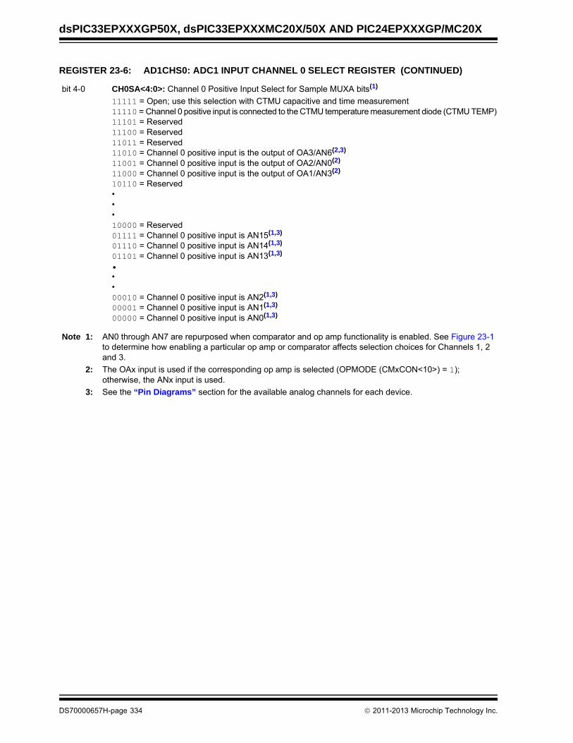
dsPIC33EPXXXGP50X, dsPIC33EPXXXMC20X/50X AND PIC24EPXXXGP/MC20X
bit 4-0 CH0SA<4:0>: Channel 0 Positive Input Select for Sample MUXA bits(1)
11111 = Open; use this selection with CTMU capacitive and time measurement11110 = Channel 0 positive input is connected to the CTMU temperature measurement diode (CTMU TEMP)11101 = Reserved11100 = Reserved11011 = Reserved11010 = Channel 0 positive input is the output of OA3/AN6(2,3)
11001 = Channel 0 positive input is the output of OA2/AN0(2)
11000 = Channel 0 positive input is the output of OA1/AN3(2)
10110 = Reserved•••10000 = Reserved01111 = Channel 0 positive input is AN15(1,3)
01110 = Channel 0 positive input is AN14(1,3)
01101 = Channel 0 positive input is AN13(1,3)
•••00010 = Channel 0 positive input is AN2(1,3)
00001 = Channel 0 positive input is AN1(1,3)
00000 = Channel 0 positive input is AN0(1,3)
REGISTER 23-6: AD1CHS0: ADC1 INPUT CHANNEL 0 SELECT REGISTER (CONTINUED)
Note 1: AN0 through AN7 are repurposed when comparator and op amp functionality is enabled. See Figure 23-1 to determine how enabling a particular op amp or comparator affects selection choices for Channels 1, 2 and 3.
2: The OAx input is used if the corresponding op amp is selected (OPMODE (CMxCON<10>) = 1); otherwise, the ANx input is used.
3: See the “Pin Diagrams” section for the available analog channels for each device.
DS70000657H-page 334 2011-2013 Microchip Technology Inc.

dsPIC33EPXXXGP50X, dsPIC33EPXXXMC20X/50X AND PIC24EPXXXGP/MC20X
REGISTER 23-7: AD1CSSH: ADC1 INPUT SCAN SELECT REGISTER HIGH(1)
R/W-0 R/W-0 U-0 U-0 U-0 R/W-0 R/W-0 R/W-0
CSS31 CSS30 — — — CSS26(2) CSS25(2) CSS24(2)
bit 15 bit 8
U-0 U-0 U-0 U-0 U-0 U-0 U-0 U-0
— — — — — — — —
bit 7 bit 0
Legend:
R = Readable bit W = Writable bit U = Unimplemented bit, read as ‘0’
-n = Value at POR ‘1’ = Bit is set ‘0’ = Bit is cleared x = Bit is unknown
bit 15 CSS31: ADC1 Input Scan Selection bit
1 = Selects CTMU capacitive and time measurement for input scan (Open)0 = Skips CTMU capacitive and time measurement for input scan (Open)
bit 14 CSS30: ADC1 Input Scan Selection bit
1 = Selects CTMU on-chip temperature measurement for input scan (CTMU TEMP)0 = Skips CTMU on-chip temperature measurement for input scan (CTMU TEMP)
bit 13-11 Unimplemented: Read as ‘0’
bit 10 CSS26: ADC1 Input Scan Selection bit(2)
1 = Selects OA3/AN6 for input scan0 = Skips OA3/AN6 for input scan
bit 9 CSS25: ADC1 Input Scan Selection bit(2)
1 = Selects OA2/AN0 for input scan0 = Skips OA2/AN0 for input scan
bit 8 CSS24: ADC1 Input Scan Selection bit(2)
1 = Selects OA1/AN3 for input scan0 = Skips OA1/AN3 for input scan
bit 7-0 Unimplemented: Read as ‘0’
Note 1: All AD1CSSH bits can be selected by user software. However, inputs selected for scan, without a corresponding input on the device, convert VREFL.
2: The OAx input is used if the corresponding op amp is selected (OPMODE (CMxCON<10>) = 1); otherwise, the ANx input is used.
2011-2013 Microchip Technology Inc. DS70000657H-page 335

dsPIC33EPXXXGP50X, dsPIC33EPXXXMC20X/50X AND PIC24EPXXXGP/MC20X
REGISTER 23-8: AD1CSSL: ADC1 INPUT SCAN SELECT REGISTER LOW(1,2)
R/W-0 R/W-0 R/W-0 R/W-0 R/W-0 R/W-0 R/W-0 R/W-0
CSS15 CSS14 CSS13 CSS12 CSS11 CSS10 CSS9 CSS8
bit 15 bit 8
R/W-0 R/W-0 R/W-0 R/W-0 R/W-0 R/W-0 R/W-0 R/W-0
CSS7 CSS6 CSS5 CSS4 CSS3 CSS2 CSS1 CSS0
bit 7 bit 0
Legend:
R = Readable bit W = Writable bit U = Unimplemented bit, read as ‘0’
-n = Value at POR ‘1’ = Bit is set ‘0’ = Bit is cleared x = Bit is unknown
bit 15-0 CSS<15:0>: ADC1 Input Scan Selection bits
1 = Selects ANx for input scan0 = Skips ANx for input scan
Note 1: On devices with less than 16 analog inputs, all AD1CSSL bits can be selected by the user. However, inputs selected for scan, without a corresponding input on the device, convert VREFL.
2: CSSx = ANx, where x = 0-15.
DS70000657H-page 336 2011-2013 Microchip Technology Inc.

dsPIC33EPXXXGP50X, dsPIC33EPXXXMC20X/50X AND PIC24EPXXXGP/MC20X
24.0 PERIPHERAL TRIGGER GENERATOR (PTG) MODULE
24.1 Module Introduction
The Peripheral Trigger Generator (PTG) provides ameans to schedule complex high-speed peripheraloperations that would be difficult to achieve using soft-ware. The PTG module uses 8-bit commands, called“Steps”, that the user writes to the PTG Queueregisters (PTGQUE0-PTGQUE7), which perform oper-ations, such as wait for input signal, generate outputtrigger and wait for timer.
The PTG module has the following major features:
• Multiple clock sources
• Two 16-bit general purpose timers
• Two 16-bit general limit counters
• Configurable for rising or falling edge triggering
• Generates processor interrupts to include:
- Four configurable processor interrupts
- Interrupt on a Step event in Single-Step mode
- Interrupt on a PTG Watchdog Timer time-out
• Able to receive trigger signals from these peripherals:
- ADC
- PWM
- Output Compare
- Input Capture
- Op Amp/Comparator
- INT2
• Able to trigger or synchronize to these peripherals:
- Watchdog Timer
- Output Compare
- Input Capture
- ADC
- PWM
- Op Amp/Comparator
Note 1: This data sheet summarizes thefeatures of the dsPIC33EPXXXGP50X,dsPIC33EPXXXMC20X/50X andPIC24EPXXXGP/MC20X families ofdevices. It is not intended to be acomprehensive reference source. Tocomplement the information in this datasheet, refer to “Peripheral TriggerGenerator (PTG)” (DS70669) in the“dsPIC33/PIC24 Family ReferenceManual”, which is available from theMicrochip web site (www.microchip.com).
2: Some registers and associated bitsdescribed in this section may not beavailable on all devices. Refer toSection 4.0 “Memory Organization” inthis data sheet for device-specific registerand bit information.
2011-2013 Microchip Technology Inc. DS70000657H-page 337

dsPIC33EPXXXGP50X, dsPIC33EPXXXMC20X/50X AND PIC24EPXXXGP/MC20X
FIGURE 24-1: PTG BLOCK DIAGRAM
16-
Bit
Dat
a B
us
PTGQPTR<4:0>
CommandDecoder
PTGHOLD
PTGADJ
PTG WatchdogTimer(1)
PTG Control Logic
PTGWDTIF
PTG GeneralPurposeTimerx
PTG LoopCounter x
Clo
ck I
npu
tsFP
TAD
T1CLKT2CLKT3CLK
PTGCLK<2:0>
PTGL0<15:0> PTGTxLIM<15:0> PTGCxLIM<15:0>
PTGBTE<15:0>
PTGO0
PTGSDLIM<15:0>
PTG StepDelay Timer
PWMOC1OC2IC1
CMPxADCINT2
PTGCON<15:0>
PT
G I
nte
rru
pts
Tri
gge
r O
utp
uts
AD1CHS0<15:0>
Step Command
Step Command
PTGSTEPIF
Tri
gger
Inp
uts
PTGO31
•••
PTG0IF
PTG3IF
•••
Step Command
Step Command
FOSC
PTGDIV<4:0>
PTGCST<15:0>
Note 1: This is a dedicated Watchdog Timer for the PTG module and is independent of the device Watchdog Timer.
PTGQUE0
PTGQUE1
PTGQUE2
PTGQUE3
PTGQUE5
PTGQUE4
PTGQUE6
PTGQUE7
DS70000657H-page 338 2011-2013 Microchip Technology Inc.

dsPIC33EPXXXGP50X, dsPIC33EPXXXMC20X/50X AND PIC24EPXXXGP/MC20X
24.2 PTG Resources
Many useful resources are provided on the main prod-uct page of the Microchip web site for the devices listedin this data sheet. This product page, which can beaccessed using this link, contains the latest updatesand additional information.
24.2.1 KEY RESOURCES
• “Peripheral Trigger Generator” (DS70669) in the “dsPIC33/PIC24 Family Reference Manual”
• Code Samples
• Application Notes
• Software Libraries
• Webinars
• All Related “dsPIC33/PIC24 Family Reference Manual” Sections
• Development Tools
Note: In the event you are not able to access theproduct page using the link above, enterthis URL in your browser:http://www.microchip.com/wwwproducts/Devices.aspx?dDocName=en555464
2011-2013 Microchip Technology Inc. DS70000657H-page 339

dsPIC33EPXXXGP50X, dsPIC33EPXXXMC20X/50X AND PIC24EPXXXGP/MC20X
24.3 PTG Control Registers
REGISTER 24-1: PTGCST: PTG CONTROL/STATUS REGISTER
R/W-0 U-0 R/W-0 R/W-0 U-0 R/W-0 R/W-0 R/W-0
PTGEN — PTGSIDL PTGTOGL — PTGSWT(2) PTGSSEN(3) PTGIVIS
bit 15 bit 8
R/W-0 HS-0 U-0 U-0 U-0 U-0 R/W-0
PTGSTRT PTGWDTO — — — — PTGITM1(1) PTGITM0(1)
bit 7 bit 0
Legend: HS = Hardware Settable bit
R = Readable bit W = Writable bit U = Unimplemented bit, read as ‘0’
-n = Value at POR ‘1’ = Bit is set ‘0’ = Bit is cleared x = Bit is unknown
bit 15 PTGEN: Module Enable bit
1 = PTG module is enabled0 = PTG module is disabled
bit 14 Unimplemented: Read as ‘0’
bit 13 PTGSIDL: PTG Stop in Idle Mode bit
1 = Discontinues module operation when device enters Idle mode0 = Continues module operation in Idle mode
bit 12 PTGTOGL: PTG TRIG Output Toggle Mode bit
1 = Toggle state of the PTGOx for each execution of the PTGTRIG command0 = Each execution of the PTGTRIG command will generate a single PTGOx pulse determined by the
value in the PTGPWDx bits
bit 11 Unimplemented: Read as ‘0’
bit 10 PTGSWT: PTG Software Trigger bit(2)
1 = Triggers the PTG module0 = No action (clearing this bit will have no effect)
bit 9 PTGSSEN: PTG Enable Single-Step bit(3)
1 = Enables Single-Step mode0 = Disables Single-Step mode
bit 8 PTGIVIS: PTG Counter/Timer Visibility Control bit
1 = Reads of the PTGSDLIM, PTGCxLIM or PTGTxLIM registers return the current values of theircorresponding counter/timer registers (PTGSD, PTGCx, PTGTx)
0 = Reads of the PTGSDLIM, PTGCxLIM or PTGTxLIM registers return the value previously writtento those limit registers
bit 7 PTGSTRT: PTG Start Sequencer bit
1 = Starts to sequentially execute commands (Continuous mode)0 = Stops executing commands
bit 6 PTGWDTO: PTG Watchdog Timer Time-out Status bit
1 = PTG Watchdog Timer has timed out0 = PTG Watchdog Timer has not timed out.
bit 5-2 Unimplemented: Read as ‘0’
Note 1: These bits apply to the PTGWHI and PTGWLO commands only.
2: This bit is only used with the PTGCTRL step command software trigger option.
3: Use of the PTG Single-Step mode is reserved for debugging tools only.
DS70000657H-page 340 2011-2013 Microchip Technology Inc.

dsPIC33EPXXXGP50X, dsPIC33EPXXXMC20X/50X AND PIC24EPXXXGP/MC20X
bit 1-0 PTGITM<1:0>: PTG Input Trigger Command Operating Mode bits(1)
11 = Single level detect with Step delay not executed on exit of command (regardless of the PTGCTRLcommand)
10 = Single level detect with Step delay executed on exit of command01 = Continuous edge detect with Step delay not executed on exit of command (regardless of the
PTGCTRL command)00 = Continuous edge detect with Step delay executed on exit of command
REGISTER 24-1: PTGCST: PTG CONTROL/STATUS REGISTER (CONTINUED)
Note 1: These bits apply to the PTGWHI and PTGWLO commands only.
2: This bit is only used with the PTGCTRL step command software trigger option.
3: Use of the PTG Single-Step mode is reserved for debugging tools only.
2011-2013 Microchip Technology Inc. DS70000657H-page 341

dsPIC33EPXXXGP50X, dsPIC33EPXXXMC20X/50X AND PIC24EPXXXGP/MC20X
REGISTER 24-2: PTGCON: PTG CONTROL REGISTER
R/W-0 R/W-0 R/W-0 R/W-0 R/W-0 R/W-0 R/W-0 R/W-0
PTGCLK2 PTGCLK1 PTGCLK0 PTGDIV4 PTGDIV3 PTGDIV2 PTGDIV1 PTGDIV0
bit 15 bit 8
R/W-0 R/W-0 R/W-0 R/W-0 U-0 R/W-0 R/W-0 R/W-0
PTGPWD3 PTGPWD2 PTGPWD1 PTGPWD0 — PTGWDT2 PTGWDT1 PTGWDT0
bit 7 bit 0
Legend:
R = Readable bit W = Writable bit U = Unimplemented bit, read as ‘0’
-n = Value at POR ‘1’ = Bit is set ‘0’ = Bit is cleared x = Bit is unknown
bit 15-13 PTGCLK<2:0>: Select PTG Module Clock Source bits
111 = Reserved110 = Reserved101 = PTG module clock source will be T3CLK100 = PTG module clock source will be T2CLK011 = PTG module clock source will be T1CLK010 = PTG module clock source will be TAD
001 = PTG module clock source will be FOSC
000 = PTG module clock source will be FP
bit 12-8 PTGDIV<4:0>: PTG Module Clock Prescaler (divider) bits
11111 = Divide-by-3211110 = Divide-by-31•••00001 = Divide-by-200000 = Divide-by-1
bit 7-4 PTGPWD<3:0>: PTG Trigger Output Pulse-Width bits
1111 = All trigger outputs are 16 PTG clock cycles wide1110 = All trigger outputs are 15 PTG clock cycles wide•••0001 = All trigger outputs are 2 PTG clock cycles wide0000 = All trigger outputs are 1 PTG clock cycle wide
bit 3 Unimplemented: Read as ‘0’
bit 2-0 PTGWDT<2:0>: Select PTG Watchdog Timer Time-out Count Value bits
111 = Watchdog Timer will time-out after 512 PTG clocks110 = Watchdog Timer will time-out after 256 PTG clocks101 = Watchdog Timer will time-out after 128 PTG clocks100 = Watchdog Timer will time-out after 64 PTG clocks011 = Watchdog Timer will time-out after 32 PTG clocks010 = Watchdog Timer will time-out after 16 PTG clocks001 = Watchdog Timer will time-out after 8 PTG clocks000 = Watchdog Timer is disabled
DS70000657H-page 342 2011-2013 Microchip Technology Inc.

dsPIC33EPXXXGP50X, dsPIC33EPXXXMC20X/50X AND PIC24EPXXXGP/MC20X
REGISTER 24-3: PTGBTE: PTG BROADCAST TRIGGER ENABLE REGISTER(1,2)
R/W-0 R/W-0 R/W-0 R/W-0 R/W-0 R/W-0 R/W-0 R/W-0
ADCTS4 ADCTS3 ADCTS2 ADCTS1 IC4TSS IC3TSS IC2TSS IC1TSS
bit 15 bit 8
R/W-0 R/W-0 R/W-0 R/W-0 R/W-0 R/W-0 R/W-0 R/W-0
OC4CS OC3CS OC2CS OC1CS OC4TSS OC3TSS OC2TSS OC1TSS
bit 7 bit 0
Legend:
R = Readable bit W = Writable bit U = Unimplemented bit, read as ‘0’
-n = Value at POR ‘1’ = Bit is set ‘0’ = Bit is cleared x = Bit is unknown
bit 15 ADCTS4: Sample Trigger PTGO15 for ADC bit
1 = Generates Trigger when the broadcast command is executed0 = Does not generate Trigger when the broadcast command is executed
bit 14 ADCTS3: Sample Trigger PTGO14 for ADC bit
1 = Generates Trigger when the broadcast command is executed0 = Does not generate Trigger when the broadcast command is executed
bit 13 ADCTS2: Sample Trigger PTGO13 for ADC bit
1 = Generates Trigger when the broadcast command is executed0 = Does not generate Trigger when the broadcast command is executed
bit 12 ADCTS1: Sample Trigger PTGO12 for ADC bit
1 = Generates Trigger when the broadcast command is executed0 = Does not generate Trigger when the broadcast command is executed
bit 11 IC4TSS: Trigger/Synchronization Source for IC4 bit
1 = Generates Trigger/Synchronization when the broadcast command is executed0 = Does not generate Trigger/Synchronization when the broadcast command is executed
bit 10 IC3TSS: Trigger/Synchronization Source for IC3 bit
1 = Generates Trigger/Synchronization when the broadcast command is executed0 = Does not generate Trigger/Synchronization when the broadcast command is executed
bit 9 IC2TSS: Trigger/Synchronization Source for IC2 bit
1 = Generates Trigger/Synchronization when the broadcast command is executed0 = Does not generate Trigger/Synchronization when the broadcast command is executed
bit 8 IC1TSS: Trigger/Synchronization Source for IC1 bit
1 = Generates Trigger/Synchronization when the broadcast command is executed0 = Does not generate Trigger/Synchronization when the broadcast command is executed
bit 7 OC4CS: Clock Source for OC4 bit
1 = Generates clock pulse when the broadcast command is executed0 = Does not generate clock pulse when the broadcast command is executed
bit 6 OC3CS: Clock Source for OC3 bit
1 = Generates clock pulse when the broadcast command is executed0 = Does not generate clock pulse when the broadcast command is executed
bit 5 OC2CS: Clock Source for OC2 bit
1 = Generates clock pulse when the broadcast command is executed0 = Does not generate clock pulse when the broadcast command is executed
Note 1: This register is read-only when the PTG module is executing Step commands (PTGEN = 1 and PTGSTRT = 1).
2: This register is only used with the PTGCTRL OPTION = 1111 Step command.
2011-2013 Microchip Technology Inc. DS70000657H-page 343

dsPIC33EPXXXGP50X, dsPIC33EPXXXMC20X/50X AND PIC24EPXXXGP/MC20X
bit 4 OC1CS: Clock Source for OC1 bit
1 = Generates clock pulse when the broadcast command is executed0 = Does not generate clock pulse when the broadcast command is executed
bit 3 OC4TSS: Trigger/Synchronization Source for OC4 bit
1 = Generates Trigger/Synchronization when the broadcast command is executed0 = Does not generate Trigger/Synchronization when the broadcast command is executed
bit 2 OC3TSS: Trigger/Synchronization Source for OC3 bit
1 = Generates Trigger/Synchronization when the broadcast command is executed0 = Does not generate Trigger/Synchronization when the broadcast command is executed
bit 1 OC2TSS: Trigger/Synchronization Source for OC2 bit
1 = Generates Trigger/Synchronization when the broadcast command is executed0 = Does not generate Trigger/Synchronization when the broadcast command is executed
bit 0 OC1TSS: Trigger/Synchronization Source for OC1 bit
1 = Generates Trigger/Synchronization when the broadcast command is executed0 = Does not generate Trigger/Synchronization when the broadcast command is executed
REGISTER 24-3: PTGBTE: PTG BROADCAST TRIGGER ENABLE REGISTER(1,2) (CONTINUED)
Note 1: This register is read-only when the PTG module is executing Step commands (PTGEN = 1 and PTGSTRT = 1).
2: This register is only used with the PTGCTRL OPTION = 1111 Step command.
DS70000657H-page 344 2011-2013 Microchip Technology Inc.

dsPIC33EPXXXGP50X, dsPIC33EPXXXMC20X/50X AND PIC24EPXXXGP/MC20X
REGISTER 24-4: PTGT0LIM: PTG TIMER0 LIMIT REGISTER(1)
R/W-0 R/W-0 R/W-0 R/W-0 R/W-0 R/W-0 R/W-0 R/W-0
PTGT0LIM<15:8>
bit 15 bit 8
R/W-0 R/W-0 R/W-0 R/W-0 R/W-0 R/W-0 R/W-0 R/W-0
PTGT0LIM<7:0>
bit 7 bit 0
Legend:
R = Readable bit W = Writable bit U = Unimplemented bit, read as ‘0’
-n = Value at POR ‘1’ = Bit is set ‘0’ = Bit is cleared x = Bit is unknown
bit 15-0 PTGT0LIM<15:0>: PTG Timer0 Limit Register bits
General Purpose Timer0 Limit register (effective only with a PTGT0 Step command).
Note 1: This register is read-only when the PTG module is executing Step commands (PTGEN = 1 and PTGSTRT = 1).
REGISTER 24-5: PTGT1LIM: PTG TIMER1 LIMIT REGISTER(1)
R/W-0 R/W-0 R/W-0 R/W-0 R/W-0 R/W-0 R/W-0 R/W-0
PTGT1LIM<15:8>
bit 15 bit 8
R/W-0 R/W-0 R/W-0 R/W-0 R/W-0 R/W-0 R/W-0 R/W-0
PTGT1LIM<7:0>
bit 7 bit 0
Legend:
R = Readable bit W = Writable bit U = Unimplemented bit, read as ‘0’
-n = Value at POR ‘1’ = Bit is set ‘0’ = Bit is cleared x = Bit is unknown
bit 15-0 PTGT1LIM<15:0>: PTG Timer1 Limit Register bits
General Purpose Timer1 Limit register (effective only with a PTGT1 Step command).
Note 1: This register is read-only when the PTG module is executing Step commands (PTGEN = 1 and PTGSTRT = 1).
2011-2013 Microchip Technology Inc. DS70000657H-page 345

dsPIC33EPXXXGP50X, dsPIC33EPXXXMC20X/50X AND PIC24EPXXXGP/MC20X
REGISTER 24-6: PTGSDLIM: PTG STEP DELAY LIMIT REGISTER(1,2)
R/W-0 R/W-0 R/W-0 R/W-0 R/W-0 R/W-0 R/W-0 R/W-0
PTGSDLIM<15:8>
bit 15 bit 8
R/W-0 R/W-0 R/W-0 R/W-0 R/W-0 R/W-0 R/W-0 R/W-0
PTGSDLIM<7:0>
bit 7 bit 0
Legend:
R = Readable bit W = Writable bit U = Unimplemented bit, read as ‘0’
-n = Value at POR ‘1’ = Bit is set ‘0’ = Bit is cleared x = Bit is unknown
bit 15-0 PTGSDLIM<15:0>: PTG Step Delay Limit Register bits
Holds a PTG Step delay value representing the number of additional PTG clocks between the start of a Step command and the completion of a Step command.
Note 1: A base Step delay of one PTG clock is added to any value written to the PTGSDLIM register (Step Delay = (PTGSDLIM) + 1).
2: This register is read-only when the PTG module is executing Step commands (PTGEN = 1 and PTGSTRT = 1).
REGISTER 24-7: PTGC0LIM: PTG COUNTER 0 LIMIT REGISTER(1)
R/W-0 R/W-0 R/W-0 R/W-0 R/W-0 R/W-0 R/W-0 R/W-0
PTGC0LIM<15:8>
bit 15 bit 8
R/W-0 R/W-0 R/W-0 R/W-0 R/W-0 R/W-0 R/W-0 R/W-0
PTGC0LIM<7:0>
bit 7 bit 0
Legend:
R = Readable bit W = Writable bit U = Unimplemented bit, read as ‘0’
-n = Value at POR ‘1’ = Bit is set ‘0’ = Bit is cleared x = Bit is unknown
bit 15-0 PTGC0LIM<15:0>: PTG Counter 0 Limit Register bits
May be used to specify the loop count for the PTGJMPC0 Step command or as a limit register for the General Purpose Counter 0.
Note 1: This register is read-only when the PTG module is executing Step commands (PTGEN = 1 and PTGSTRT = 1).
DS70000657H-page 346 2011-2013 Microchip Technology Inc.

dsPIC33EPXXXGP50X, dsPIC33EPXXXMC20X/50X AND PIC24EPXXXGP/MC20X
REGISTER 24-8: PTGC1LIM: PTG COUNTER 1 LIMIT REGISTER(1)
R/W-0 R/W-0 R/W-0 R/W-0 R/W-0 R/W-0 R/W-0 R/W-0
PTGC1LIM<15:8>
bit 15 bit 8
R/W-0 R/W-0 R/W-0 R/W-0 R/W-0 R/W-0 R/W-0 R/W-0
PTGC1LIM<7:0>
bit 7 bit 0
Legend:
R = Readable bit W = Writable bit U = Unimplemented bit, read as ‘0’
-n = Value at POR ‘1’ = Bit is set ‘0’ = Bit is cleared x = Bit is unknown
bit 15-0 PTGC1LIM<15:0>: PTG Counter 1 Limit Register bits
May be used to specify the loop count for the PTGJMPC1 Step command or as a limit register for the General Purpose Counter 1.
Note 1: This register is read-only when the PTG module is executing Step commands (PTGEN = 1 and PTGSTRT = 1).
REGISTER 24-9: PTGHOLD: PTG HOLD REGISTER(1)
R/W-0 R/W-0 R/W-0 R/W-0 R/W-0 R/W-0 R/W-0 R/W-0
PTGHOLD<15:8>
bit 15 bit 8
R/W-0 R/W-0 R/W-0 R/W-0 R/W-0 R/W-0 R/W-0 R/W-0
PTGHOLD<7:0>
bit 7 bit 0
Legend:
R = Readable bit W = Writable bit U = Unimplemented bit, read as ‘0’
-n = Value at POR ‘1’ = Bit is set ‘0’ = Bit is cleared x = Bit is unknown
bit 15-0 PTGHOLD<15:0>: PTG General Purpose Hold Register bits
Holds user-supplied data to be copied to the PTGTxLIM, PTGCxLIM, PTGSDLIM or PTGL0 registers with the PTGCOPY command.
Note 1: This register is read-only when the PTG module is executing Step commands (PTGEN = 1 and PTGSTRT = 1).
2011-2013 Microchip Technology Inc. DS70000657H-page 347

dsPIC33EPXXXGP50X, dsPIC33EPXXXMC20X/50X AND PIC24EPXXXGP/MC20X
REGISTER 24-10: PTGADJ: PTG ADJUST REGISTER(1)
R/W-0 R/W-0 R/W-0 R/W-0 R/W-0 R/W-0 R/W-0 R/W-0
PTGADJ<15:8>
bit 15 bit 8
R/W-0 R/W-0 R/W-0 R/W-0 R/W-0 R/W-0 R/W-0 R/W-0
PTGADJ<7:0>
bit 7 bit 0
Legend:
R = Readable bit W = Writable bit U = Unimplemented bit, read as ‘0’
-n = Value at POR ‘1’ = Bit is set ‘0’ = Bit is cleared x = Bit is unknown
bit 15-0 PTGADJ<15:0>: PTG Adjust Register bits
This register holds user-supplied data to be added to the PTGTxLIM, PTGCxLIM, PTGSDLIM or PTGL0 registers with the PTGADD command.
Note 1: This register is read-only when the PTG module is executing Step commands (PTGEN = 1 and PTGSTRT = 1).
REGISTER 24-11: PTGL0: PTG LITERAL 0 REGISTER(1)
R/W-0 R/W-0 R/W-0 R/W-0 R/W-0 R/W-0 R/W-0 R/W-0
PTGL0<15:8>
bit 15 bit 8
R/W-0 R/W-0 R/W-0 R/W-0 R/W-0 R/W-0 R/W-0 R/W-0
PTGL0<7:0>
bit 7 bit 0
Legend:
R = Readable bit W = Writable bit U = Unimplemented bit, read as ‘0’
-n = Value at POR ‘1’ = Bit is set ‘0’ = Bit is cleared x = Bit is unknown
bit 15-0 PTGL0<15:0>: PTG Literal 0 Register bits
This register holds the 16-bit value to be written to the AD1CHS0 register with the PTGCTRL Step command.
Note 1: This register is read-only when the PTG module is executing Step commands (PTGEN = 1 and PTGSTRT = 1).
DS70000657H-page 348 2011-2013 Microchip Technology Inc.

dsPIC33EPXXXGP50X, dsPIC33EPXXXMC20X/50X AND PIC24EPXXXGP/MC20X
REGISTER 24-12: PTGQPTR: PTG STEP QUEUE POINTER REGISTER(1)
U-0 U-0 U-0 U-0 U-0 U-0 U-0 U-0
— — — — — — — —
bit 15 bit 8
U-0 U-0 U-0 R/W-0 R/W-0 R/W-0 R/W-0 R/W-0
— — — PTGQPTR<4:0>
bit 7 bit 0
Legend:
R = Readable bit W = Writable bit U = Unimplemented bit, read as ‘0’
-n = Value at POR ‘1’ = Bit is set ‘0’ = Bit is cleared x = Bit is unknown
bit 15-5 Unimplemented: Read as ‘0’
bit 4-0 PTGQPTR<4:0>: PTG Step Queue Pointer Register bits
This register points to the currently active Step command in the Step queue.
Note 1: This register is read-only when the PTG module is executing Step commands (PTGEN = 1 and PTGSTRT = 1).
REGISTER 24-13: PTGQUEx: PTG STEP QUEUE REGISTER x (x = 0-7)(1,3)
R/W-0 R/W-0 R/W-0 R/W-0 R/W-0 R/W-0 R/W-0 R/W-0
STEP(2x + 1)<7:0>(2)
bit 15 bit 8
R/W-0 R/W-0 R/W-0 R/W-0 R/W-0 R/W-0 R/W-0 R/W-0
STEP(2x)<7:0>(2)
bit 7 bit 0
Legend:
R = Readable bit W = Writable bit U = Unimplemented bit, read as ‘0’
-n = Value at POR ‘1’ = Bit is set ‘0’ = Bit is cleared x = Bit is unknown
bit 15-8 STEP(2x + 1)<7:0>: PTG Step Queue Pointer Register bits(2)
A queue location for storage of the STEP(2x + 1) command byte.
bit 7-0 STEP(2x)<7:0>: PTG Step Queue Pointer Register bits(2)
A queue location for storage of the STEP(2x) command byte.
Note 1: This register is read-only when the PTG module is executing Step commands (PTGEN = 1 and PTGSTRT = 1).
2: Refer to Table 24-1 for the Step command encoding.
3: The Step registers maintain their values on any type of Reset.
2011-2013 Microchip Technology Inc. DS70000657H-page 349
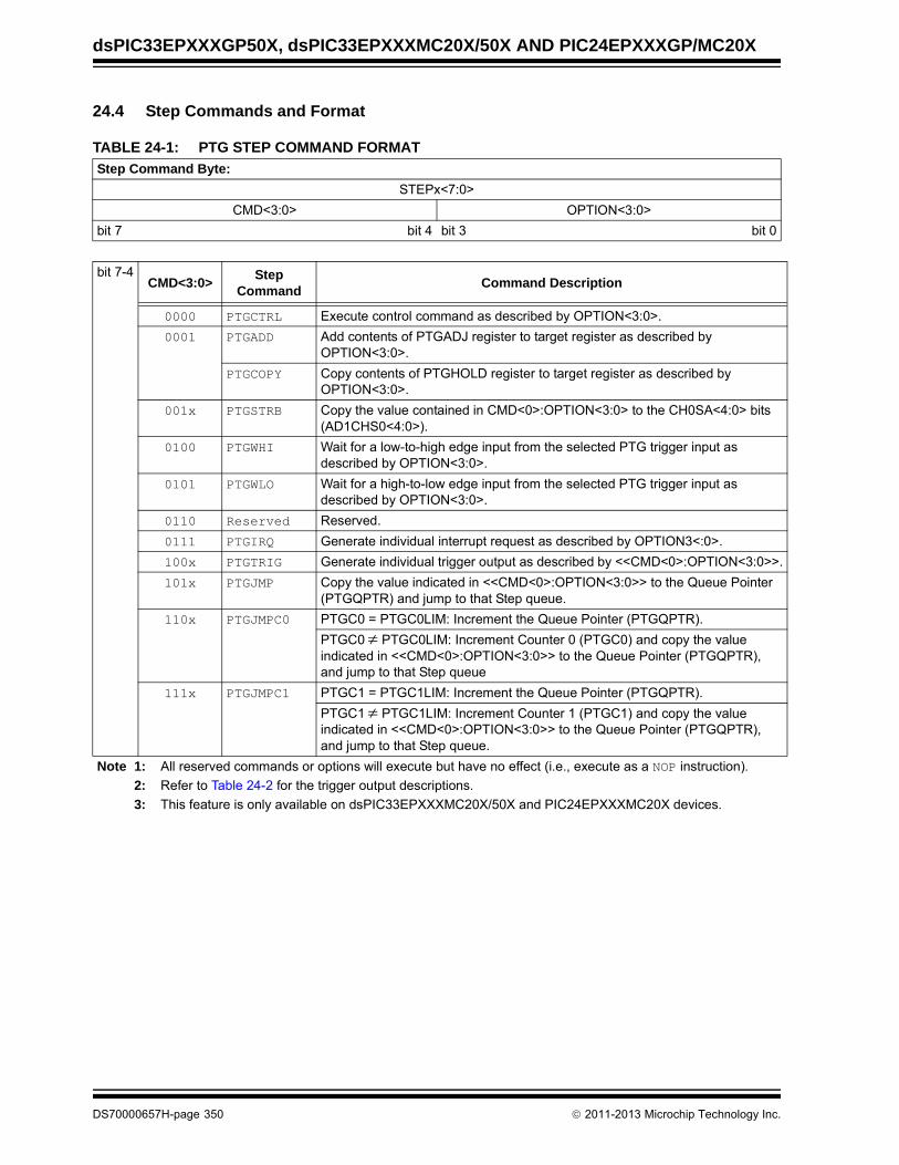
dsPIC33EPXXXGP50X, dsPIC33EPXXXMC20X/50X AND PIC24EPXXXGP/MC20X
24.4 Step Commands and Format
TABLE 24-1: PTG STEP COMMAND FORMAT
Step Command Byte:
STEPx<7:0>
CMD<3:0> OPTION<3:0>
bit 7 bit 4 bit 3 bit 0
bit 7-4CMD<3:0>
Step Command
Command Description
0000 PTGCTRL Execute control command as described by OPTION<3:0>.
0001 PTGADD Add contents of PTGADJ register to target register as described by OPTION<3:0>.
PTGCOPY Copy contents of PTGHOLD register to target register as described by OPTION<3:0>.
001x PTGSTRB Copy the value contained in CMD<0>:OPTION<3:0> to the CH0SA<4:0> bits (AD1CHS0<4:0>).
0100 PTGWHI Wait for a low-to-high edge input from the selected PTG trigger input as described by OPTION<3:0>.
0101 PTGWLO Wait for a high-to-low edge input from the selected PTG trigger input as described by OPTION<3:0>.
0110 Reserved Reserved.
0111 PTGIRQ Generate individual interrupt request as described by OPTION3<:0>.
100x PTGTRIG Generate individual trigger output as described by <<CMD<0>:OPTION<3:0>>.
101x PTGJMP Copy the value indicated in <<CMD<0>:OPTION<3:0>> to the Queue Pointer (PTGQPTR) and jump to that Step queue.
110x PTGJMPC0 PTGC0 = PTGC0LIM: Increment the Queue Pointer (PTGQPTR).
PTGC0 PTGC0LIM: Increment Counter 0 (PTGC0) and copy the value indicated in <<CMD<0>:OPTION<3:0>> to the Queue Pointer (PTGQPTR), and jump to that Step queue
111x PTGJMPC1 PTGC1 = PTGC1LIM: Increment the Queue Pointer (PTGQPTR).
PTGC1 PTGC1LIM: Increment Counter 1 (PTGC1) and copy the value indicated in <<CMD<0>:OPTION<3:0>> to the Queue Pointer (PTGQPTR), and jump to that Step queue.
Note 1: All reserved commands or options will execute but have no effect (i.e., execute as a NOP instruction).
2: Refer to Table 24-2 for the trigger output descriptions.
3: This feature is only available on dsPIC33EPXXXMC20X/50X and PIC24EPXXXMC20X devices.
DS70000657H-page 350 2011-2013 Microchip Technology Inc.

dsPIC33EPXXXGP50X, dsPIC33EPXXXMC20X/50X AND PIC24EPXXXGP/MC20X
TABLE 24-1: PTG STEP COMMAND FORMAT (CONTINUED)
bit 3-0 Step Command
OPTION<3:0> Option Description
PTGCTRL(1) 0000 Reserved.
0001 Reserved.
0010 Disable Step Delay Timer (PTGSD).
0011 Reserved.
0100 Reserved.
0101 Reserved.
0110 Enable Step Delay Timer (PTGSD).
0111 Reserved.
1000 Start and wait for the PTG Timer0 to match the Timer0 Limit Register.
1001 Start and wait for the PTG Timer1 to match the Timer1 Limit Register.
1010 Reserved.
1011 Wait for the software trigger bit transition from low-to-high before continuing (PTGSWT = 0 to 1).
1100 Copy contents of the Counter 0 register to the AD1CHS0 register.
1101 Copy contents of the Counter 1 register to the AD1CHS0 register.
1110 Copy contents of the Literal 0 register to the AD1CHS0 register.
1111 Generate triggers indicated in the Broadcast Trigger Enable register (PTGBTE).
PTGADD(1) 0000 Add contents of the PTGADJ register to the Counter 0 Limit register (PTGC0LIM).
0001 Add contents of the PTGADJ register to the Counter 1 Limit register (PTGC1LIM).
0010 Add contents of the PTGADJ register to the Timer0 Limit register (PTGT0LIM).
0011 Add contents of the PTGADJ register to the Timer1 Limit register (PTGT1LIM).
0100 Add contents of the PTGADJ register to the Step Delay Limit register (PTGSDLIM).
0101 Add contents of the PTGADJ register to the Literal 0 register (PTGL0).
0110 Reserved.
0111 Reserved.
PTGCOPY(1) 1000 Copy contents of the PTGHOLD register to the Counter 0 Limit register (PTGC0LIM).
1001 Copy contents of the PTGHOLD register to the Counter 1 Limit register (PTGC1LIM).
1010 Copy contents of the PTGHOLD register to the Timer0 Limit register (PTGT0LIM).
1011 Copy contents of the PTGHOLD register to the Timer1 Limit register (PTGT1LIM).
1100 Copy contents of the PTGHOLD register to the Step Delay Limit register (PTGSDLIM).
1101 Copy contents of the PTGHOLD register to the Literal 0 register (PTGL0).
1110 Reserved.
1111 Reserved.
Note 1: All reserved commands or options will execute but have no effect (i.e., execute as a NOP instruction).
2: Refer to Table 24-2 for the trigger output descriptions.
3: This feature is only available on dsPIC33EPXXXMC20X/50X and PIC24EPXXXMC20X devices.
2011-2013 Microchip Technology Inc. DS70000657H-page 351

dsPIC33EPXXXGP50X, dsPIC33EPXXXMC20X/50X AND PIC24EPXXXGP/MC20X
TABLE 24-1: PTG STEP COMMAND FORMAT (CONTINUED)
bit 3-0 Step Command
OPTION<3:0> Option Description
PTGWHI(1) or PTGWLO(1)
0000 PWM Special Event Trigger.(3)
0001 PWM master time base synchronization output.(3)
0010 PWM1 interrupt.(3)
0011 PWM2 interrupt.(3)
0100 PWM3 interrupt.(3)
0101 Reserved.
0110 Reserved.
0111 OC1 Trigger event.
1000 OC2 Trigger event.
1001 IC1 Trigger event.
1010 CMP1 Trigger event.
1011 CMP2 Trigger event.
1100 CMP3 Trigger event.
1101 CMP4 Trigger event.
1110 ADC conversion done interrupt.
1111 INT2 external interrupt.
PTGIRQ(1) 0000 Generate PTG Interrupt 0.
0001 Generate PTG Interrupt 1.
0010 Generate PTG Interrupt 2.
0011 Generate PTG Interrupt 3.
0100 Reserved.
•
•
•
•
•
•
1111 Reserved.
PTGTRIG(2) 00000 PTGO0.
00001 PTGO1.
•
•
•
•
•
•
11110 PTGO30.
11111 PTGO31.
Note 1: All reserved commands or options will execute but have no effect (i.e., execute as a NOP instruction).
2: Refer to Table 24-2 for the trigger output descriptions.
3: This feature is only available on dsPIC33EPXXXMC20X/50X and PIC24EPXXXMC20X devices.
DS70000657H-page 352 2011-2013 Microchip Technology Inc.

dsPIC33EPXXXGP50X, dsPIC33EPXXXMC20X/50X AND PIC24EPXXXGP/MC20X
TABLE 24-2: PTG OUTPUT DESCRIPTIONS
PTG Output Number
PTG Output Description
PTGO0 Trigger/Synchronization Source for OC1
PTGO1 Trigger/Synchronization Source for OC2
PTGO2 Trigger/Synchronization Source for OC3
PTGO3 Trigger/Synchronization Source for OC4
PTGO4 Clock Source for OC1
PTGO5 Clock Source for OC2
PTGO6 Clock Source for OC3
PTGO7 Clock Source for OC4
PTGO8 Trigger/Synchronization Source for IC1
PTGO9 Trigger/Synchronization Source for IC2
PTGO10 Trigger/Synchronization Source for IC3
PTGO11 Trigger/Synchronization Source for IC4
PTGO12 Sample Trigger for ADC
PTGO13 Sample Trigger for ADC
PTGO14 Sample Trigger for ADC
PTGO15 Sample Trigger for ADC
PTGO16 PWM Time Base Synchronous Source for PWM(1)
PTGO17 PWM Time Base Synchronous Source for PWM(1)
PTGO18 Mask Input Select for Op Amp/Comparator
PTGO19 Mask Input Select for Op Amp/Comparator
PTGO20 Reserved
PTGO21 Reserved
PTGO22 Reserved
PTGO23 Reserved
PTGO24 Reserved
PTGO25 Reserved
PTGO26 Reserved
PTGO27 Reserved
PTGO28 Reserved
PTGO29 Reserved
PTGO30 PTG Output to PPS Input Selection
PTGO31 PTG Output to PPS Input Selection
Note 1: This feature is only available on dsPIC33EPXXXMC20X/50X and PIC24EPXXXMC20X devices.
2011-2013 Microchip Technology Inc. DS70000657H-page 353

dsPIC33EPXXXGP50X, dsPIC33EPXXXMC20X/50X AND PIC24EPXXXGP/MC20X
NOTES:
DS70000657H-page 354 2011-2013 Microchip Technology Inc.

dsPIC33EPXXXGP50X, dsPIC33EPXXXMC20X/50X AND PIC24EPXXXGP/MC20X
25.0 OP AMP/COMPARATOR MODULE
The dsPIC33EPXXXGP50X, dsPIC33EPXXXMC20X/50X and PIC24EPXXXGP/MC20X devices contain upto four comparators, which can be configured in variousways. Comparators, CMP1, CMP2 and CMP3, alsohave the option to be configured as op amps, with theoutput being brought to an external pin for gain/filteringconnections. As shown in Figure 25-1, individualcomparator options are specified by the comparatormodule’s Special Function Register (SFR) control bits.
These options allow users to:
• Select the edge for trigger and interrupt generation
• Configure the comparator voltage reference
• Configure output blanking and masking
• Configure as a comparator or op amp (CMP1, CMP2 and CMP3 only)
FIGURE 25-1: OP AMP/COMPARATOR x MODULE BLOCK DIAGRAM (MODULES 1, 2 AND 3)
Note 1: This data sheet summarizes thefeatures of the dsPIC33EPXXXGP50X,dsPIC33EPXXXMC20X/50X andPIC24EPXXXGP/MC20X families ofdevices. It is not intended to be a compre-hensive reference source. To complementthe information in this data sheet, refer to“Op Amp/Comparator” (DS70357) in the“dsPIC33/PIC24 Family Reference Man-ual”, which is available from the Microchipweb site (www.microchip.com).
2: Some registers and associated bitsdescribed in this section may not beavailable on all devices. Refer toSection 4.0 “Memory Organization” inthis data sheet for device-specific registerand bit information.
Note: Op Amp/Comparator 3 is not available onthe dsPIC33EPXXXGP502/MC502/MC202and PIC24EP256GP/MC202 (28-pin)devices.
Note: Not all op amp/comparator input/outputconnections are available on all devices.See the “Pin Diagrams” section foravailable connections.
BlankingFunction
DigitalFilter
CxOUT(1)
(see Figure 25-4) (see Figure 25-5) PTG TriggerInput0
1
00
01
CxIN1+
CVREFIN(1)
CxIN1-
CXIN2-(1)
Note 1: This input/output is not available as a selection when configured as an op amp (OPMODE (CMxCON<10>) = 1).2: This module can be configured either as an op amp or a comparator using the OPMODE bit.3: When configured as an op amp (OPMODE = 1), the ADC samples the op amp output; otherwise, the ADC
samples the ANx pin.
CMPx
–
+
VIN-
VIN+
CCH<1:0> (CMxCON<1:0>)
CREF (CMxCON<4>)
Op Amp/Comparator(2)
Op Ampx–
+OAx/ANx(3)
OAxOUT/ANx
OPMODE (CMxCON<10>)
(to ADC)
RINT1
2011-2013 Microchip Technology Inc. DS70000657H-page 355

dsPIC33EPXXXGP50X, dsPIC33EPXXXMC20X/50X AND PIC24EPXXXGP/MC20X
FIGURE 25-2: COMPARATOR MODULE BLOCK DIAGRAM (MODULE 4)
FIGURE 25-3: OP AMP/COMPARATOR VOLTAGE REFERENCE BLOCK DIAGRAM
CMP4BlankingFunction
DigitalFilter
(see Figure 25-4) (see Figure 25-5)
–
+VIN+
C4OUT
TriggerOutputC4IN1+
CVREFIN
VIN-
1
0
11
00
CCH<1:0> (CM4CON<1:0>)
OA3/AN6
C4IN1-
CREF (CMxCON<4>)
01
10
OA1/AN3
OA2/AN0
8R
RCVREN
CVRSS = 0AVDD
VREF+CVRSS = 1(1)
8R
R
R
R
R
R
R
16 Steps
CVRR
CVREF1O
CV
R3
CV
R2
CV
R1
CV
R0
CVRCON<3:0>
AVSS
CVRSRC
CVR1OE
CVREFIN
VREFSEL
CVREF2O(2)
CVR2OE
Note 1: In order to operate with CVRSS = 1, at least one of the comparator modules must be enabled.2: This reference is (AVDD + AVSS)/2.
AVSS
AVDD
1
0
16
-to
-1 M
UX
(CVRCON<6>)
(CVRCON<14>)
(CVRCON<10>)
DS70000657H-page 356 2011-2013 Microchip Technology Inc.

dsPIC33EPXXXGP50X, dsPIC33EPXXXMC20X/50X AND PIC24EPXXXGP/MC20X
FIGURE 25-4: USER-PROGRAMMABLE BLANKING FUNCTION BLOCK DIAGRAM
FIGURE 25-5: DIGITAL FILTER INTERCONNECT BLOCK DIAGRAM
SELSRCA<3:0>
SELSRCB<3:0>
SELSRCC<3:0>
AND
CMxMSKCON
MU
X A MAI
MBI
MCI
Comparator Output To Digital
Signals
Filter
OR
Blanking
Blanking
BlankingSignals
Signals
ANDI
MASK
“AND-OR” Function
HLMS
MU
X B
MU
X C
BlankingLogic
(CMxMSKCON<15)
(CMxMSKSRC<11:8)
(CMxMSKSRC<7:4)
(CMxMSKSRC<3:0>)
MBI
MCI
MAI
MBI
MCI
MAI
CXOUT
CFLTREN
Digital Filter
TxCLK(1,2)
SYNCO1(3)
FP(4)
FOSC(4)
CFSEL<2:0>
CFDIV
Note 1: See the Type C Timer Block Diagram (Figure 13-2).2: See the Type B Timer Block Diagram (Figure 13-1).3: See the High-Speed PWMx Module Register Interconnection Diagram (Figure 16-2).4: See the Oscillator System Diagram (Figure 9-1).
From Blanking Logic
1xx
010
000
001
1
0
(CMxFLTR<6:4>) (CMxFLTR<3>)
2011-2013 Microchip Technology Inc. DS70000657H-page 357
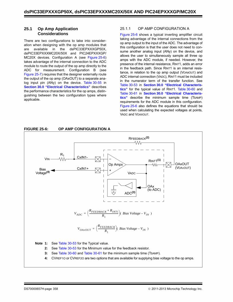
dsPIC33EPXXXGP50X, dsPIC33EPXXXMC20X/50X AND PIC24EPXXXGP/MC20X
25.1 Op Amp Application Considerations
There are two configurations to take into consider-ation when designing with the op amp modules thatare available in the dsPIC33EPXXXGP50X,dsPIC33EPXXXMC20X/50X and PIC24EPXXXGP/MC20X devices. Configuration A (see Figure 25-6)takes advantage of the internal connection to the ADCmodule to route the output of the op amp directly to theADC for measurement. Configuration B (seeFigure 25-7) requires that the designer externally routethe output of the op amp (OAxOUT) to a separate ana-log input pin (ANy) on the device. Table 30-55 inSection 30.0 “Electrical Characteristics” describesthe performance characteristics for the op amps, distin-guishing between the two configuration types whereapplicable.
25.1.1 OP AMP CONFIGURATION A
Figure 25-6 shows a typical inverting amplifier circuittaking advantage of the internal connections from theop amp output to the input of the ADC. The advantage ofthis configuration is that the user does not need to con-sume another analog input (ANy) on the device, andallows the user to simultaneously sample all three opamps with the ADC module, if needed. However, thepresence of the internal resistance, RINT1, adds an errorin the feedback path. Since RINT1 is an internal resis-tance, in relation to the op amp output (VOAxOUT) andADC internal connection (VADC), RINT1 must be includedin the numerator term of the transfer function. SeeTable 30-53 in Section 30.0 “Electrical Characteris-tics” for the typical value of RINT1. Table 30-60 andTable 30-61 in Section 30.0 “Electrical Characteris-tics” describe the minimum sample time (TSAMP)requirements for the ADC module in this configuration.Figure 25-6 also defines the equations that should beused when calculating the expected voltages at points,VADC and VOAXOUT.
FIGURE 25-6: OP AMP CONFIGURATION A
–
+
CxIN1-
CxIN1+
R1
ADC(3)
OAxOUTRINT1(1)
RFEEDBACK(2)
OAx(to ADC)
Op Ampx
Note 1: See Table 30-53 for the Typical value.
2: See Table 30-53 for the Minimum value for the feedback resistor.
3: See Table 30-60 and Table 30-61 for the minimum sample time (TSAMP).
4: CVREF1O or CVREF2O are two options that are available for supplying bias voltage to the op amps.
VIN
VADC
(VOAXOUT)
VOAxOUT
RFEEDBACK
R1------------------------------ Bias Voltage V– IN =
VADC
RFEEDBACK RINT1+
R1--------------------------------------------------- Bias Voltage V– IN =
BiasVoltage(4)
DS70000657H-page 358 2011-2013 Microchip Technology Inc.

dsPIC33EPXXXGP50X, dsPIC33EPXXXMC20X/50X AND PIC24EPXXXGP/MC20X
25.1.2 OP AMP CONFIGURATION B
Figure 25-7 shows a typical inverting amplifier circuitwith the output of the op amp (OAxOUT) externallyrouted to a separate analog input pin (ANy) on thedevice. This op amp configuration is slightly different interms of the op amp output and the ADC inputconnection, therefore, RINT1 is not included in thetransfer function. However, this configuration requiresthe designer to externally route the op amp output(OAxOUT) to another analog input pin (ANy). SeeTable 30-53 in Section 30.0 “Electrical Characteris-tics” for the typical value of RINT1. Table 30-60 andTable 30-61 in Section 30.0 “Electrical Characteris-tics” describe the minimum sample time (TSAMP)requirements for the ADC module in this configuration.
Figure 25-7 also defines the equation to be used tocalculate the expected voltage at point VOAXOUT. Thisis the typical inverting amplifier equation.
25.2 Op Amp/Comparator Resources
Many useful resources are provided on the main prod-uct page of the Microchip web site for the devices listedin this data sheet. This product page, which can beaccessed using this link, contains the latest updatesand additional information.
25.2.1 KEY RESOURCES
• “Op Amp/Comparator” (DS70357) in the “dsPIC33/PIC24 Family Reference Manual”
• Code Samples
• Application Notes
• Software Libraries
• Webinars
• All Related “dsPIC33/PIC24 Family Reference Manual” Sections
• Development Tools
FIGURE 25-7: OP AMP CONFIGURATION B
Note: In the event you are not able to access theproduct page using the link above, enterthis URL in your browser:http://www.microchip.com/wwwproducts/Devices.aspx?dDocName=en555464
ADC(3)
OAxOUT
RFEEDBACK(2)
ANy
Note 1: See Table 30-53 for the Typical value.
2: See Table 30-53 for the Minimum value for the feedback resistor.
3: See Table 30-60 and Table 30-61 for the minimum sample time (TSAMP).
4: CVREF1O or CVREF2O are two options that are available for supplying bias voltage to the op amps.
–
+
Op Ampx(VOAXOUT)
RINT1(1)
VOAxOUT
RFEEDBACK
R1------------------------------ Bias Voltage V– IN =
CxIN1-
CxIN1+
R1
VIN
BiasVoltage(4)
2011-2013 Microchip Technology Inc. DS70000657H-page 359

dsPIC33EPXXXGP50X, dsPIC33EPXXXMC20X/50X AND PIC24EPXXXGP/MC20X
25.3 Op Amp/Comparator Registers
REGISTER 25-1: CMSTAT: OP AMP/COMPARATOR STATUS REGISTER
R/W-0 U-0 U-0 U-0 R-0 R-0 R-0 R-0
PSIDL — — — C4EVT(1) C3EVT(1) C2EVT(1) C1EVT(1)
bit 15 bit 8
U-0 U-0 U-0 U-0 R-0 R-0 R-0 R-0
— — — — C4OUT(2) C3OUT(2) C2OUT(2) C1OUT(2)
bit 7 bit 0
Legend:
R = Readable bit W = Writable bit U = Unimplemented bit, read as ‘0’
-n = Value at POR ‘1’ = Bit is set ‘0’ = Bit is cleared x = Bit is unknown
bit 15 PSIDL: Comparator Stop in Idle Mode bit
1 = Discontinues operation of all comparators when device enters Idle mode0 = Continues operation of all comparators in Idle mode
bit 14-12 Unimplemented: Read as ‘0’
bit 11 C4EVT: Op Amp/Comparator 4 Event Status bit(1)
1 = Op amp/comparator event occurred0 = Op amp/comparator event did not occur
bit 10 C3EVT: Comparator 3 Event Status bit(1)
1 = Comparator event occurred0 = Comparator event did not occur
bit 9 C2EVT: Comparator 2 Event Status bit(1)
1 = Comparator event occurred0 = Comparator event did not occur
bit 8 C1EVT: Comparator 1 Event Status bit(1)
1 = Comparator event occurred0 = Comparator event did not occur
bit 7-4 Unimplemented: Read as ‘0’
bit 3 C4OUT: Comparator 4 Output Status bit(2)
When CPOL = 0:1 = VIN+ > VIN-0 = VIN+ < VIN-
When CPOL = 1:1 = VIN+ < VIN-0 = VIN+ > VIN-
bit 2 C3OUT: Comparator 3 Output Status bit(2)
When CPOL = 0:1 = VIN+ > VIN-0 = VIN+ < VIN-
When CPOL = 1:1 = VIN+ < VIN-0 = VIN+ > VIN-
Note 1: Reflects the value of the of the CEVT bit in the respective Op Amp/Comparator Control register, CMxCON<9>.
2: Reflects the value of the COUT bit in the respective Op Amp/Comparator Control register, CMxCON<8>.
DS70000657H-page 360 2011-2013 Microchip Technology Inc.

dsPIC33EPXXXGP50X, dsPIC33EPXXXMC20X/50X AND PIC24EPXXXGP/MC20X
bit 1 C2OUT: Comparator 2 Output Status bit(2)
When CPOL = 0:1 = VIN+ > VIN-0 = VIN+ < VIN-
When CPOL = 1:1 = VIN+ < VIN-0 = VIN+ > VIN-
bit 0 C1OUT: Comparator 1 Output Status bit(2)
When CPOL = 0:1 = VIN+ > VIN-0 = VIN+ < VIN-
When CPOL = 1:1 = VIN+ < VIN-0 = VIN+ > VIN-
REGISTER 25-1: CMSTAT: OP AMP/COMPARATOR STATUS REGISTER (CONTINUED)
Note 1: Reflects the value of the of the CEVT bit in the respective Op Amp/Comparator Control register, CMxCON<9>.
2: Reflects the value of the COUT bit in the respective Op Amp/Comparator Control register, CMxCON<8>.
2011-2013 Microchip Technology Inc. DS70000657H-page 361

dsPIC33EPXXXGP50X, dsPIC33EPXXXMC20X/50X AND PIC24EPXXXGP/MC20X
REGISTER 25-2: CMxCON: COMPARATOR x CONTROL REGISTER (x = 1, 2 OR 3)
R/W-0 R/W-0 R/W-0 U-0 U-0 R/W-0 R/W-0 R/W-0
CON COE(2) CPOL — — OPMODE CEVT COUT
bit 15 bit 8
R/W-0 R/W-0 U-0 R/W-0 U-0 U-0 R/W-0 R/W-0
EVPOL1 EVPOL0 — CREF(1) — — CCH1(1) CCH0(1)
bit 7 bit 0
Legend:
R = Readable bit W = Writable bit U = Unimplemented bit, read as ‘0’
-n = Value at POR ‘1’ = Bit is set ‘0’ = Bit is cleared x = Bit is unknown
bit 15 CON: Op Amp/Comparator Enable bit
1 = Op amp/comparator is enabled0 = Op amp/comparator is disabled
bit 14 COE: Comparator Output Enable bit(2)
1 = Comparator output is present on the CxOUT pin0 = Comparator output is internal only
bit 13 CPOL: Comparator Output Polarity Select bit
1 = Comparator output is inverted0 = Comparator output is not inverted
bit 12-11 Unimplemented: Read as ‘0’
bit 10 OPMODE: Op Amp/Comparator Operation Mode Select bit
1 = Circuit operates as an op amp0 = Circuit operates as a comparator
bit 9 CEVT: Comparator Event bit
1 = Comparator event according to the EVPOL<1:0> settings occurred; disables future triggers andinterrupts until the bit is cleared
0 = Comparator event did not occur
bit 8 COUT: Comparator Output bit
When CPOL = 0 (non-inverted polarity):1 = VIN+ > VIN-0 = VIN+ < VIN-
When CPOL = 1 (inverted polarity):1 = VIN+ < VIN-0 = VIN+ > VIN-
Note 1: Inputs that are selected and not available will be tied to VSS. See the “Pin Diagrams” section for available inputs for each package.
2: This output is not available when OPMODE (CMxCON<10>) = 1.
DS70000657H-page 362 2011-2013 Microchip Technology Inc.
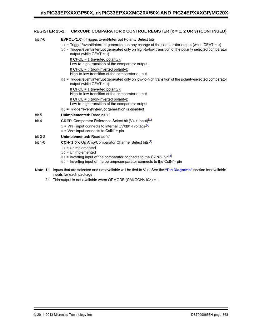
dsPIC33EPXXXGP50X, dsPIC33EPXXXMC20X/50X AND PIC24EPXXXGP/MC20X
bit 7-6 EVPOL<1:0>: Trigger/Event/Interrupt Polarity Select bits
11 = Trigger/event/interrupt generated on any change of the comparator output (while CEVT = 0)10 = Trigger/event/interrupt generated only on high-to-low transition of the polarity selected comparator
output (while CEVT = 0)
If CPOL = 1 (inverted polarity):Low-to-high transition of the comparator output.
If CPOL = 0 (non-inverted polarity):High-to-low transition of the comparator output.
01 = Trigger/event/interrupt generated only on low-to-high transition of the polarity-selected comparatoroutput (while CEVT = 0)
If CPOL = 1 (inverted polarity):High-to-low transition of the comparator output.
If CPOL = 0 (non-inverted polarity):Low-to-high transition of the comparator output
00 = Trigger/event/interrupt generation is disabled
bit 5 Unimplemented: Read as ‘0’
bit 4 CREF: Comparator Reference Select bit (VIN+ input)(1)
1 = VIN+ input connects to internal CVREFIN voltage(2)
0 = VIN+ input connects to CxIN1+ pin
bit 3-2 Unimplemented: Read as ‘0’
bit 1-0 CCH<1:0>: Op Amp/Comparator Channel Select bits(1)
11 = Unimplemented10 = Unimplemented01 = Inverting input of the comparator connects to the CxIN2- pin(2)
00 = Inverting input of the op amp/comparator connects to the CxIN1- pin
REGISTER 25-2: CMxCON: COMPARATOR x CONTROL REGISTER (x = 1, 2 OR 3) (CONTINUED)
Note 1: Inputs that are selected and not available will be tied to VSS. See the “Pin Diagrams” section for available inputs for each package.
2: This output is not available when OPMODE (CMxCON<10>) = 1.
2011-2013 Microchip Technology Inc. DS70000657H-page 363
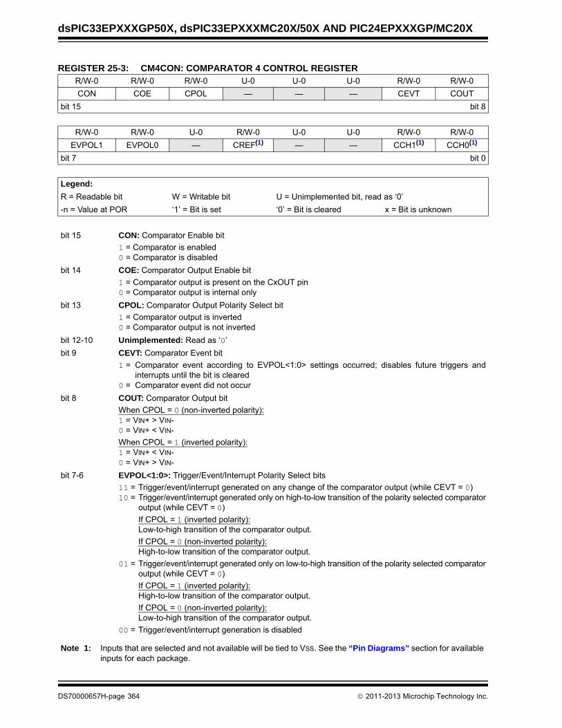
dsPIC33EPXXXGP50X, dsPIC33EPXXXMC20X/50X AND PIC24EPXXXGP/MC20X
REGISTER 25-3: CM4CON: COMPARATOR 4 CONTROL REGISTERR/W-0 R/W-0 R/W-0 U-0 U-0 U-0 R/W-0 R/W-0
CON COE CPOL — — — CEVT COUT
bit 15 bit 8
R/W-0 R/W-0 U-0 R/W-0 U-0 U-0 R/W-0 R/W-0
EVPOL1 EVPOL0 — CREF(1) — — CCH1(1) CCH0(1)
bit 7 bit 0
Legend:
R = Readable bit W = Writable bit U = Unimplemented bit, read as ‘0’
-n = Value at POR ‘1’ = Bit is set ‘0’ = Bit is cleared x = Bit is unknown
bit 15 CON: Comparator Enable bit
1 = Comparator is enabled0 = Comparator is disabled
bit 14 COE: Comparator Output Enable bit
1 = Comparator output is present on the CxOUT pin0 = Comparator output is internal only
bit 13 CPOL: Comparator Output Polarity Select bit
1 = Comparator output is inverted0 = Comparator output is not inverted
bit 12-10 Unimplemented: Read as ‘0’
bit 9 CEVT: Comparator Event bit
1 = Comparator event according to EVPOL<1:0> settings occurred; disables future triggers andinterrupts until the bit is cleared
0 = Comparator event did not occur
bit 8 COUT: Comparator Output bit
When CPOL = 0 (non-inverted polarity):1 = VIN+ > VIN-0 = VIN+ < VIN-
When CPOL = 1 (inverted polarity):1 = VIN+ < VIN-0 = VIN+ > VIN-
bit 7-6 EVPOL<1:0>: Trigger/Event/Interrupt Polarity Select bits
11 = Trigger/event/interrupt generated on any change of the comparator output (while CEVT = 0)10 = Trigger/event/interrupt generated only on high-to-low transition of the polarity selected comparator
output (while CEVT = 0)
If CPOL = 1 (inverted polarity):Low-to-high transition of the comparator output.
If CPOL = 0 (non-inverted polarity):High-to-low transition of the comparator output.
01 = Trigger/event/interrupt generated only on low-to-high transition of the polarity selected comparatoroutput (while CEVT = 0)
If CPOL = 1 (inverted polarity):High-to-low transition of the comparator output.
If CPOL = 0 (non-inverted polarity):Low-to-high transition of the comparator output.
00 = Trigger/event/interrupt generation is disabled
Note 1: Inputs that are selected and not available will be tied to VSS. See the “Pin Diagrams” section for available inputs for each package.
DS70000657H-page 364 2011-2013 Microchip Technology Inc.

dsPIC33EPXXXGP50X, dsPIC33EPXXXMC20X/50X AND PIC24EPXXXGP/MC20X
bit 5 Unimplemented: Read as ‘0’
bit 4 CREF: Comparator Reference Select bit (VIN+ input)(1)
1 = VIN+ input connects to internal CVREFIN voltage0 = VIN+ input connects to C4IN1+ pin
bit 3-2 Unimplemented: Read as ‘0’
bit 1-0 CCH<1:0>: Comparator Channel Select bits(1)
11 = VIN- input of comparator connects to OA3/AN610 = VIN- input of comparator connects to OA2/AN001 = VIN- input of comparator connects to OA1/AN3 00 = VIN- input of comparator connects to C4IN1-
REGISTER 25-3: CM4CON: COMPARATOR 4 CONTROL REGISTER (CONTINUED)
Note 1: Inputs that are selected and not available will be tied to VSS. See the “Pin Diagrams” section for available inputs for each package.
2011-2013 Microchip Technology Inc. DS70000657H-page 365

dsPIC33EPXXXGP50X, dsPIC33EPXXXMC20X/50X AND PIC24EPXXXGP/MC20X
REGISTER 25-4: CMxMSKSRC: COMPARATOR x MASK SOURCE SELECT CONTROL REGISTER
U-0 U-0 U-0 U-0 R/W-0 R/W-0 R/W-0 RW-0
— — — — SELSRCC3 SELSRCC2 SELSRCC1 SELSRCC0
bit 15 bit 8
R/W-0 R/W-0 R/W-0 R/W-0 R/W-0 R/W-0 R/W-0 R/W-0
SELSRCB3 SELSRCB2 SELSRCB1 SELSRCB0 SELSRCA3 SELSRCA2 SELSRCA1 SELSRCA0
bit 7 bit 0
Legend:
R = Readable bit W = Writable bit U = Unimplemented bit, read as ‘0’
-n = Value at POR ‘1’ = Bit is set ‘0’ = Bit is cleared x = Bit is unknown
bit 15-12 Unimplemented: Read as ‘0’
bit 11-8 SELSRCC<3:0>: Mask C Input Select bits
1111 = FLT41110 = FLT21101 = PTGO191100 = PTGO181011 = Reserved1010 = Reserved1001 = Reserved1000 = Reserved0111 = Reserved0110 = Reserved0101 = PWM3H0100 = PWM3L0011 = PWM2H0010 = PWM2L0001 = PWM1H0000 = PWM1L
bit 7-4 SELSRCB<3:0>: Mask B Input Select bits
1111 = FLT41110 = FLT21101 = PTGO191100 = PTGO181011 = Reserved1010 = Reserved1001 = Reserved1000 = Reserved0111 = Reserved0110 = Reserved0101 = PWM3H0100 = PWM3L0011 = PWM2H0010 = PWM2L0001 = PWM1H0000 = PWM1L
DS70000657H-page 366 2011-2013 Microchip Technology Inc.

dsPIC33EPXXXGP50X, dsPIC33EPXXXMC20X/50X AND PIC24EPXXXGP/MC20X
bit 3-0 SELSRCA<3:0>: Mask A Input Select bits
1111 = FLT41110 = FLT21101 = PTGO191100 = PTGO181011 = Reserved1010 = Reserved1001 = Reserved1000 = Reserved0111 = Reserved0110 = Reserved0101 = PWM3H0100 = PWM3L0011 = PWM2H0010 = PWM2L0001 = PWM1H0000 = PWM1L
REGISTER 25-4: CMxMSKSRC: COMPARATOR x MASK SOURCE SELECT CONTROL REGISTER (CONTINUED)
2011-2013 Microchip Technology Inc. DS70000657H-page 367

dsPIC33EPXXXGP50X, dsPIC33EPXXXMC20X/50X AND PIC24EPXXXGP/MC20X
REGISTER 25-5: CMxMSKCON: COMPARATOR x MASK GATING CONTROL REGISTER
R/W-0 U-0 R/W-0 R/W-0 R/W-0 R/W-0 R/W-0 R/W-0
HLMS — OCEN OCNEN OBEN OBNEN OAEN OANEN
bit 15 bit 8
R/W-0 R/W-0 R/W-0 R/W-0 R/W-0 R/W-0 R/W-0 R/W-0
NAGS PAGS ACEN ACNEN ABEN ABNEN AAEN AANEN
bit 7 bit 0
Legend:
R = Readable bit W = Writable bit U = Unimplemented bit, read as ‘0’
-n = Value at POR ‘1’ = Bit is set ‘0’ = Bit is cleared x = Bit is unknown
bit 15 HLMS: High or Low-Level Masking Select bits
1 = The masking (blanking) function will prevent any asserted (‘0’) comparator signal from propagating0 = The masking (blanking) function will prevent any asserted (‘1’) comparator signal from propagating
bit 14 Unimplemented: Read as ‘0’
bit 13 OCEN: OR Gate C Input Enable bit
1 = MCI is connected to OR gate0 = MCI is not connected to OR gate
bit 12 OCNEN: OR Gate C Input Inverted Enable bit
1 = Inverted MCI is connected to OR gate0 = Inverted MCI is not connected to OR gate
bit 11 OBEN: OR Gate B Input Enable bit
1 = MBI is connected to OR gate0 = MBI is not connected to OR gate
bit 10 OBNEN: OR Gate B Input Inverted Enable bit
1 = Inverted MBI is connected to OR gate0 = Inverted MBI is not connected to OR gate
bit 9 OAEN: OR Gate A Input Enable bit
1 = MAI is connected to OR gate0 = MAI is not connected to OR gate
bit 8 OANEN: OR Gate A Input Inverted Enable bit
1 = Inverted MAI is connected to OR gate0 = Inverted MAI is not connected to OR gate
bit 7 NAGS: AND Gate Output Inverted Enable bit1 = Inverted ANDI is connected to OR gate0 = Inverted ANDI is not connected to OR gate
bit 6 PAGS: AND Gate Output Enable bit1 = ANDI is connected to OR gate0 = ANDI is not connected to OR gate
bit 5 ACEN: AND Gate C Input Enable bit
1 = MCI is connected to AND gate0 = MCI is not connected to AND gate
bit 4 ACNEN: AND Gate C Input Inverted Enable bit
1 = Inverted MCI is connected to AND gate0 = Inverted MCI is not connected to AND gate
DS70000657H-page 368 2011-2013 Microchip Technology Inc.

dsPIC33EPXXXGP50X, dsPIC33EPXXXMC20X/50X AND PIC24EPXXXGP/MC20X
bit 3 ABEN: AND Gate B Input Enable bit
1 = MBI is connected to AND gate0 = MBI is not connected to AND gate
bit 2 ABNEN: AND Gate B Input Inverted Enable bit
1 = Inverted MBI is connected to AND gate0 = Inverted MBI is not connected to AND gate
bit 1 AAEN: AND Gate A Input Enable bit
1 = MAI is connected to AND gate0 = MAI is not connected to AND gate
bit 0 AANEN: AND Gate A Input Inverted Enable bit
1 = Inverted MAI is connected to AND gate0 = Inverted MAI is not connected to AND gate
REGISTER 25-5: CMxMSKCON: COMPARATOR x MASK GATING CONTROL REGISTER (CONTINUED)
2011-2013 Microchip Technology Inc. DS70000657H-page 369

dsPIC33EPXXXGP50X, dsPIC33EPXXXMC20X/50X AND PIC24EPXXXGP/MC20X
REGISTER 25-6: CMxFLTR: COMPARATOR x FILTER CONTROL REGISTER
U-0 U-0 U-0 U-0 U-0 U-0 U-0 U-0
— — — — — — — —
bit 15 bit 8
U-0 R/W-0 R/W-0 R/W-0 R/W-0 R/W-0 R/W-0 R/W-0
— CFSEL2 CFSEL1 CFSEL0 CFLTREN CFDIV2 CFDIV1 CFDIV0
bit 7 bit 0
Legend:
R = Readable bit W = Writable bit U = Unimplemented bit, read as ‘0’
-n = Value at POR ‘1’ = Bit is set ‘0’ = Bit is cleared x = Bit is unknown
bit 15-7 Unimplemented: Read as ‘0’
bit 6-4 CFSEL<2:0>: Comparator Filter Input Clock Select bits
111 = T5CLK(1)
110 = T4CLK(2)
101 = T3CLK(1)
100 = T2CLK(2)
011 = Reserved010 = SYNCO1(3)
001 = FOSC(4)
000 = FP(4)
bit 3 CFLTREN: Comparator Filter Enable bit
1 = Digital filter is enabled0 = Digital filter is disabled
bit 2-0 CFDIV<2:0>: Comparator Filter Clock Divide Select bits
111 = Clock Divide 1:128110 = Clock Divide 1:64101 = Clock Divide 1:32100 = Clock Divide 1:16011 = Clock Divide 1:8010 = Clock Divide 1:4001 = Clock Divide 1:2000 = Clock Divide 1:1
Note 1: See the Type C Timer Block Diagram (Figure 13-2).
2: See the Type B Timer Block Diagram (Figure 13-1).
3: See the High-Speed PWMx Module Register Interconnection Diagram (Figure 16-2).
4: See the Oscillator System Diagram (Figure 9-1).
DS70000657H-page 370 2011-2013 Microchip Technology Inc.

dsPIC33EPXXXGP50X, dsPIC33EPXXXMC20X/50X AND PIC24EPXXXGP/MC20X
REGISTER 25-7: CVRCON: COMPARATOR VOLTAGE REFERENCE CONTROL REGISTER
U-0 R/W-0 U-0 U-0 U-0 R/W-0 U-0 U-0
— CVR2OE(1) — — — VREFSEL — —
bit 15 bit 8
R/W-0 R/W-0 R/W-0 R/W-0 R/W-0 R/W-0 R/W-0 R/W-0
CVREN CVR1OE(1) CVRR CVRSS(2) CVR3 CVR2 CVR1 CVR0
bit 7 bit 0
Legend:
R = Readable bit W = Writable bit U = Unimplemented bit, read as ‘0’
-n = Value at POR ‘1’ = Bit is set ‘0’ = Bit is cleared x = Bit is unknown
bit 15 Unimplemented: Read as ‘0’
bit 14 CVR2OE: Comparator Voltage Reference 2 Output Enable bit(1)
1 = (AVDD – AVSS)/2 is connected to the CVREF2O pin0 = (AVDD – AVSS)/2 is disconnected from the CVREF2O pin
bit 13-11 Unimplemented: Read as ‘0’
bit 10 VREFSEL: Comparator Voltage Reference Select bit
1 = CVREFIN = VREF+0 = CVREFIN is generated by the resistor network
bit 9-8 Unimplemented: Read as ‘0’
bit 7 CVREN: Comparator Voltage Reference Enable bit
1 = Comparator voltage reference circuit is powered on0 = Comparator voltage reference circuit is powered down
bit 6 CVR1OE: Comparator Voltage Reference 1 Output Enable bit(1)
1 = Voltage level is output on the CVREF1O pin0 = Voltage level is disconnected from then CVREF1O pin
bit 5 CVRR: Comparator Voltage Reference Range Selection bit
1 = CVRSRC/24 step-size 0 = CVRSRC/32 step-size
bit 4 CVRSS: Comparator Voltage Reference Source Selection bit(2)
1 = Comparator voltage reference source, CVRSRC = (VREF+) – (AVSS) 0 = Comparator voltage reference source, CVRSRC = AVDD – AVSS
bit 3-0 CVR<3:0> Comparator Voltage Reference Value Selection 0 CVR<3:0> 15 bits
When CVRR = 1:CVREFIN = (CVR<3:0>/24) (CVRSRC)
When CVRR = 0:CVREFIN = (CVRSRC/4) + (CVR<3:0>/32) (CVRSRC)
Note 1: CVRxOE overrides the TRISx and the ANSELx bit settings.
2: In order to operate with CVRSS = 1, at least one of the comparator modules must be enabled.
2011-2013 Microchip Technology Inc. DS70000657H-page 371

dsPIC33EPXXXGP50X, dsPIC33EPXXXMC20X/50X AND PIC24EPXXXGP/MC20X
NOTES:
DS70000657H-page 372 2011-2013 Microchip Technology Inc.
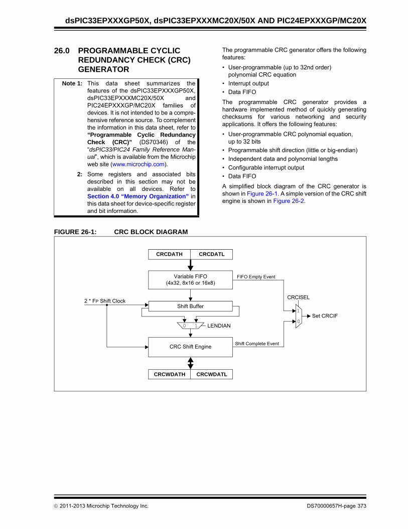
dsPIC33EPXXXGP50X, dsPIC33EPXXXMC20X/50X AND PIC24EPXXXGP/MC20X
26.0 PROGRAMMABLE CYCLIC REDUNDANCY CHECK (CRC) GENERATOR
The programmable CRC generator offers the followingfeatures:
• User-programmable (up to 32nd order) polynomial CRC equation
• Interrupt output
• Data FIFO
The programmable CRC generator provides ahardware implemented method of quickly generatingchecksums for various networking and securityapplications. It offers the following features:
• User-programmable CRC polynomial equation, up to 32 bits
• Programmable shift direction (little or big-endian)
• Independent data and polynomial lengths
• Configurable interrupt output
• Data FIFO
A simplified block diagram of the CRC generator isshown in Figure 26-1. A simple version of the CRC shiftengine is shown in Figure 26-2.
FIGURE 26-1: CRC BLOCK DIAGRAM
Note 1: This data sheet summarizes thefeatures of the dsPIC33EPXXXGP50X,dsPIC33EPXXXMC20X/50X andPIC24EPXXXGP/MC20X families ofdevices. It is not intended to be a compre-hensive reference source. To complementthe information in this data sheet, refer to“Programmable Cyclic RedundancyCheck (CRC)” (DS70346) of the“dsPIC33/PIC24 Family Reference Man-ual”, which is available from the Microchipweb site (www.microchip.com).
2: Some registers and associated bitsdescribed in this section may not beavailable on all devices. Refer toSection 4.0 “Memory Organization” inthis data sheet for device-specific registerand bit information.
Variable FIFO(4x32, 8x16 or 16x8)
CRCDATH CRCDATL
Shift Buffer
CRC Shift Engine
CRCWDATH CRCWDATL
LENDIAN10
CRCISEL
1
0
FIFO Empty Event
Shift Complete Event
Set CRCIF
2 * FP Shift Clock
2011-2013 Microchip Technology Inc. DS70000657H-page 373

dsPIC33EPXXXGP50X, dsPIC33EPXXXMC20X/50X AND PIC24EPXXXGP/MC20X
FIGURE 26-2: CRC SHIFT ENGINE DETAIL
26.1 Overview
The CRC module can be programmed for CRCpolynomials of up to the 32nd order, using up to 32 bits.Polynomial length, which reflects the highest exponentin the equation, is selected by the PLEN<4:0> bits(CRCCON2<4:0>).
The CRCXORL and CRCXORH registers control whichexponent terms are included in the equation. Setting aparticular bit includes that exponent term in theequation; functionally, this includes an XOR operationon the corresponding bit in the CRC engine. Clearingthe bit disables the XOR.
For example, consider two CRC polynomials, one a16-bit equation and the other a 32-bit equation:
To program these polynomials into the CRC generator,set the register bits as shown in Table 26-1.
Note that the appropriate positions are set to ‘1’ toindicate that they are used in the equation (for example,X26 and X23). The 0 bit required by the equation isalways XORed; thus, X0 is a don’t care. For a poly-nomial of length N, it is assumed that the Nth bit willalways be used, regardless of the bit setting. Therefore,for a polynomial length of 32, there is no 32nd bit in theCRCxOR register.
TABLE 26-1: CRC SETUP EXAMPLES FOR 16 AND 32-BIT POLYNOMIAL
26.2 Programmable CRC Resources
Many useful resources are provided on the main prod-uct page of the Microchip web site for the devices listedin this data sheet. This product page, which can beaccessed using this link, contains the latest updatesand additional information.
26.2.1 KEY RESOURCES
• “Programmable Cyclic Redundancy Check (CRC)” (DS70346) in the “dsPIC33/PIC24 Family Reference Manual”
• Code Samples
• Application Notes
• Software Libraries
• Webinars
• All Related “dsPIC33/PIC24 Family Reference Manual” Sections
• Development Tools
CRCWDATH CRCWDATL
Bit 0 Bit 1 Bit n(2)
X(1)(1)
Read/Write Bus
Shift BufferData Bit 2
X(2)(1) X(n)(1)
Note 1: Each XOR stage of the shift engine is programmable. See text for details.2: Polynomial length n is determined by ([PLEN<4:0>] + 1).
x16 + x12 + x5 + 1
and
x32 + x26 + x23 + x22 + x16 + x12 + x11 + x10 + x8 + x7 + x5 + x4 + x2 + x + 1
CRC Control Bits
Bit Values
16-bit Polynomial
32-bit Polynomial
PLEN<4:0> 01111 11111
X<31:16> 0000 0000 0000 000x
0000 0100 1100 0001
X<15:0> 0001 0000 0010 000x
0001 1101 1011 011x
Note: In the event you are not able to access theproduct page using the link above, enterthis URL in your browser:http://www.microchip.com/wwwproducts/Devices.aspx?dDocName=en555464
DS70000657H-page 374 2011-2013 Microchip Technology Inc.

dsPIC33EPXXXGP50X, dsPIC33EPXXXMC20X/50X AND PIC24EPXXXGP/MC20X
26.3 Programmable CRC Registers
REGISTER 26-1: CRCCON1: CRC CONTROL REGISTER 1
R/W-0 U-0 R/W-0 R-0 R-0 R-0 R-0 R-0
CRCEN — CSIDL VWORD4 VWORD3 VWORD2 VWORD1 VWORD0
bit 15 bit 8
R-0 R-1 R/W-0 R/W-0 R/W-0 U-0 U-0 U-0
CRCFUL CRCMPT CRCISEL CRCGO LENDIAN — — —
bit 7 bit 0
Legend:
R = Readable bit W = Writable bit U = Unimplemented bit, read as ‘0’
-n = Value at POR ‘1’ = Bit is set ‘0’ = Bit is cleared x = Bit is unknown
bit 15 CRCEN: CRC Enable bit
1 = CRC module is enabled0 = CRC module is disabled; all state machines, pointers and CRCWDAT/CRCDAT are reset, other
SFRs are not reset
bit 14 Unimplemented: Read as ‘0’
bit 13 CSIDL: CRC Stop in Idle Mode bit
1 = Discontinues module operation when device enters Idle mode0 = Continues module operation in Idle mode
bit 12-8 VWORD<4:0>: Pointer Value bits
Indicates the number of valid words in the FIFO. Has a maximum value of 8 when PLEN<4:0> > 7or 16 when PLEN<4:0> 7.
bit 7 CRCFUL: CRC FIFO Full bit
1 = FIFO is full 0 = FIFO is not full
bit 6 CRCMPT: CRC FIFO Empty Bit
1 = FIFO is empty 0 = FIFO is not empty
bit 5 CRCISEL: CRC Interrupt Selection bit
1 = Interrupt on FIFO is empty; final word of data is still shifting through CRC 0 = Interrupt on shift is complete and CRCWDAT results are ready
bit 4 CRCGO: Start CRC bit
1 = Starts CRC serial shifter0 = CRC serial shifter is turned off
bit 3 LENDIAN: Data Word Little-Endian Configuration bit
1 = Data word is shifted into the CRC starting with the LSb (little endian)0 = Data word is shifted into the CRC starting with the MSb (big endian)
bit 2-0 Unimplemented: Read as ‘0’
2011-2013 Microchip Technology Inc. DS70000657H-page 375

dsPIC33EPXXXGP50X, dsPIC33EPXXXMC20X/50X AND PIC24EPXXXGP/MC20X
REGISTER 26-2: CRCCON2: CRC CONTROL REGISTER 2
U-0 U-0 U-0 R/W-0 R/W-0 R/W-0 R/W-0 R/W-0
— — — DWIDTH4 DWIDTH3 DWIDTH2 DWIDTH1 DWIDTH0
bit 15 bit 8
U-0 U-0 U-0 R/W-0 R/W-0 R/W-0 R/W-0 R/W-0
— — — PLEN4 PLEN3 PLEN2 PLEN1 PLEN0
bit 7 bit 0
Legend:
R = Readable bit W = Writable bit U = Unimplemented bit, read as ‘0’
-n = Value at POR ‘1’ = Bit is set ‘0’ = Bit is cleared x = Bit is unknown
bit 15-13 Unimplemented: Read as ‘0’
bit 12-8 DWIDTH<4:0>: Data Width Select bits
These bits set the width of the data word (DWIDTH<4:0> + 1).
bit 7-5 Unimplemented: Read as ‘0’
bit 4-0 PLEN<4:0>: Polynomial Length Select bits
These bits set the length of the polynomial (Polynomial Length = PLEN<4:0> + 1).
DS70000657H-page 376 2011-2013 Microchip Technology Inc.
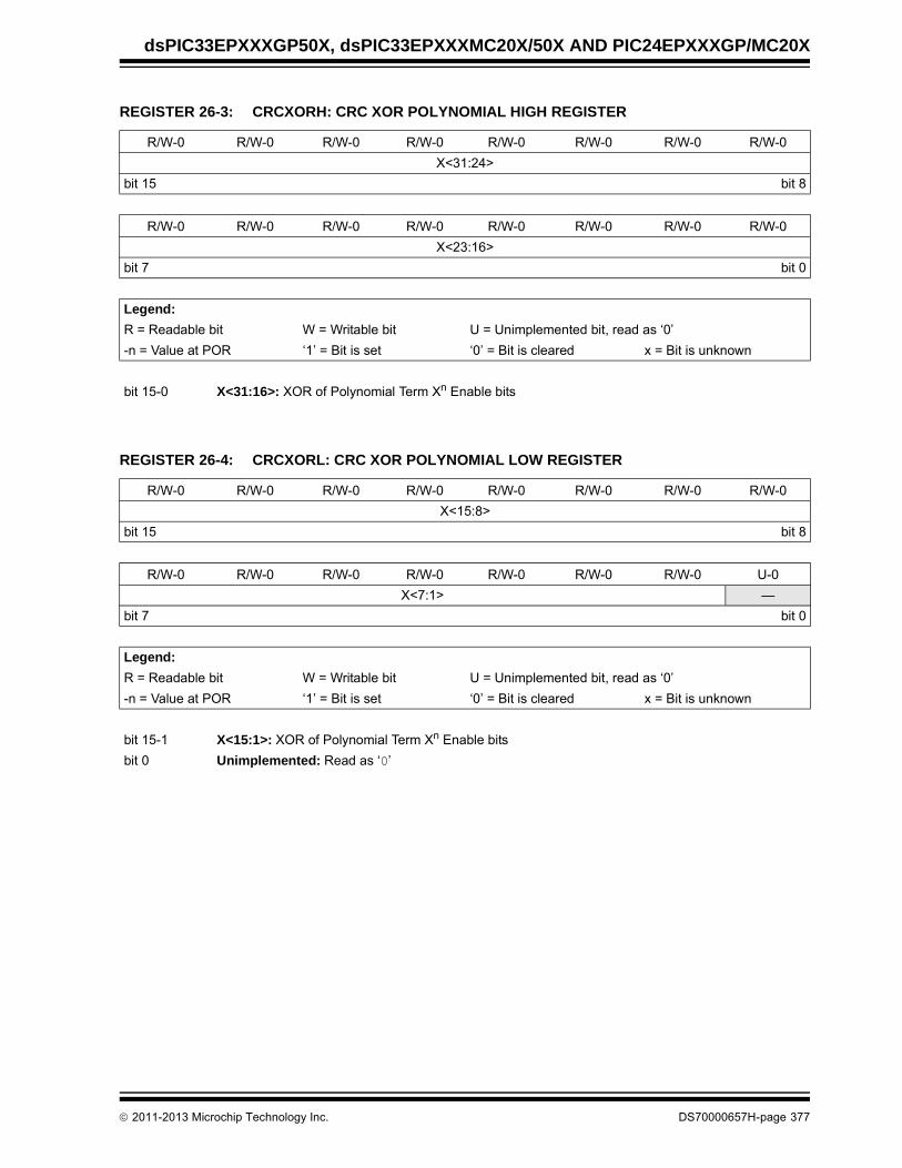
dsPIC33EPXXXGP50X, dsPIC33EPXXXMC20X/50X AND PIC24EPXXXGP/MC20X
REGISTER 26-3: CRCXORH: CRC XOR POLYNOMIAL HIGH REGISTER
R/W-0 R/W-0 R/W-0 R/W-0 R/W-0 R/W-0 R/W-0 R/W-0
X<31:24>
bit 15 bit 8
R/W-0 R/W-0 R/W-0 R/W-0 R/W-0 R/W-0 R/W-0 R/W-0
X<23:16>
bit 7 bit 0
Legend:
R = Readable bit W = Writable bit U = Unimplemented bit, read as ‘0’
-n = Value at POR ‘1’ = Bit is set ‘0’ = Bit is cleared x = Bit is unknown
bit 15-0 X<31:16>: XOR of Polynomial Term Xn Enable bits
REGISTER 26-4: CRCXORL: CRC XOR POLYNOMIAL LOW REGISTER
R/W-0 R/W-0 R/W-0 R/W-0 R/W-0 R/W-0 R/W-0 R/W-0
X<15:8>
bit 15 bit 8
R/W-0 R/W-0 R/W-0 R/W-0 R/W-0 R/W-0 R/W-0 U-0
X<7:1> —
bit 7 bit 0
Legend:
R = Readable bit W = Writable bit U = Unimplemented bit, read as ‘0’
-n = Value at POR ‘1’ = Bit is set ‘0’ = Bit is cleared x = Bit is unknown
bit 15-1 X<15:1>: XOR of Polynomial Term Xn Enable bits
bit 0 Unimplemented: Read as ‘0’
2011-2013 Microchip Technology Inc. DS70000657H-page 377

dsPIC33EPXXXGP50X, dsPIC33EPXXXMC20X/50X AND PIC24EPXXXGP/MC20X
NOTES:
DS70000657H-page 378 2011-2013 Microchip Technology Inc.

dsPIC33EPXXXGP50X, dsPIC33EPXXXMC20X/50X AND PIC24EPXXXGP/MC20X
27.0 SPECIAL FEATURES
dsPIC33EPXXXGP50X, dsPIC33EPXXXMC20X/50Xand PIC24EPXXXGP/MC20X devices include severalfeatures intended to maximize application flexibility andreliability, and minimize cost through elimination ofexternal components. These are:
• Flexible Configuration
• Watchdog Timer (WDT)
• Code Protection and CodeGuard™ Security
• JTAG Boundary Scan Interface
• In-Circuit Serial Programming™ (ICSP™)
• In-Circuit Emulation
27.1 Configuration Bits
In dsPIC33EPXXXGP50X, dsPIC33EPXXXMC20X/50X and PIC24EPXXXGP/MC20X devices, theConfiguration bytes are implemented as volatile mem-ory. This means that configuration data must beprogrammed each time the device is powered up.Configuration data is stored in at the top of the on-chipprogram memory space, known as the Flash Configura-tion bytes. Their specific locations are shown inTable 27-1. The configuration data is automaticallyloaded from the Flash Configuration bytes to the properConfiguration Shadow registers during device Resets.
When creating applications for these devices, usersshould always specifically allocate the location of theFlash Configuration bytes for configuration data in theircode for the compiler. This is to make certain that pro-gram code is not stored in this address when the codeis compiled.
The upper 2 bytes of all Flash Configuration Words inprogram memory should always be ‘1111 1111 11111111’. This makes them appear to be NOP instructionsin the remote event that their locations are everexecuted by accident. Since Configuration bits are notimplemented in the corresponding locations, writing‘1’s to these locations has no effect on deviceoperation.
The Configuration Flash bytes map is shown inTable 27-1.
Note: This data sheet summarizes thefeatures of the dsPIC33EPXXXGP50X,dsPIC33EPXXXMC20X/50X andPIC24EPXXXGP/MC20X families ofdevices. It is not intended to be acomprehensive reference source. Tocomplement the information in this datasheet, refer to the related section of the“dsPIC33/PIC24 Family ReferenceManual”, which is available from theMicrochip web site (www.microchip.com).
Note: Configuration data is reloaded on all typesof device Resets.
Note: Performing a page erase operation on thelast page of program memory clears theFlash Configuration bytes, enabling codeprotection as a result. Therefore, usersshould avoid performing page eraseoperations on the last page of programmemory.
2011-2013 Microchip Technology Inc. DS70000657H-page 379

dsPIC33EPXXXGP50X, dsPIC33EPXXXMC20X/50X AND PIC24EPXXXGP/MC20X
TABLE 27-1: CONFIGURATION BYTE REGISTER MAP
File Name
Address
Device Memory
Size (Kbytes)
Bits 23-8 Bit 7 Bit 6 Bit 5 Bit 4 Bit 3 Bit 2 Bit 1 Bit 0
Reserved 0057EC 32
— — — — — — — — —
00AFEC 64
0157EC 128
02AFEC 256
0557EC 512
Reserved 0057EE 32
— — — — — — — — —
00AFEE 64
0157EE 128
02AFEE 256
0557EE 512
FICD 0057F0 32
— Reserved(3) — JTAGEN Reserved(2) Reserved(3) — ICS<1:0>
00AFF0 64
0157F0 128
02AFF0 256
0557F0 512
FPOR 0057F2 32
— WDTWIN<1:0> ALTI2C2 ALTI2C1 Reserved(3) — — —
00AFF2 64
0157F2 128
02AFF2 256
0557F2 512
FWDT 0057F4 32
— FWDTEN WINDIS PLLKEN WDTPRE WDTPOST<3:0>
00AFF4 64
0157F4 128
02AFF4 256
0557F4 512
FOSC 0057F6 32
— FCKSM<1:0> IOL1WAY — — OSCIOFNC POSCMD<1:0>
00AFF6 64
0157F6 128
02AFF6 256
0557F6 512
FOSCSEL 0057F8 32
— IESO PWMLOCK(1) — — — FNOSC<2:0>
00AFF8 64
0157F8 128
02AFF8 256
0557F8 512
FGS 0057FA 32
— — — — — — — GCP GWRP
00AFFA 64
0157FA 128
02AFFA 256
0557FA 512
Reserved 0057FC 32
— — — — — — — — —
00AFFC 64
0157FC 128
02AFFC 256
0557FC 512
Reserved 057FFE 32
— — — — — — — — —
00AFFE 64
0157FE 128
02AFFE 256
0557FE 512
Legend: — = unimplemented, read as ‘1’.
Note 1: This bit is only available on dsPIC33EPXXXMC20X/50X and PIC24EPXXXMC20X devices.
2: This bit is reserved and must be programmed as ‘0’.
3: These bits are reserved and must be programmed as ‘1’.
DS70000657H-page 380 2011-2013 Microchip Technology Inc.

dsPIC33EPXXXGP50X, dsPIC33EPXXXMC20X/50X AND PIC24EPXXXGP/MC20X
TABLE 27-2: CONFIGURATION BITS DESCRIPTION
Bit Field Description
GCP General Segment Code-Protect bit1 = User program memory is not code-protected0 = Code protection is enabled for the entire program memory space
GWRP General Segment Write-Protect bit1 = User program memory is not write-protected0 = User program memory is write-protected
IESO Two-Speed Oscillator Start-up Enable bit1 = Start up device with FRC, then automatically switch to the user-selected oscillator
source when ready0 = Start up device with user-selected oscillator source
PWMLOCK(1) PWM Lock Enable bit1 = Certain PWM registers may only be written after a key sequence0 = PWM registers may be written without a key sequence
FNOSC<2:0> Oscillator Selection bits111 = Fast RC Oscillator with Divide-by-N (FRCDIVN)110 = Fast RC Oscillator with Divide-by-16 (FRCDIV16)101 = Low-Power RC Oscillator (LPRC)100 = Reserved; do not use011 = Primary Oscillator with PLL module (XT + PLL, HS + PLL, EC + PLL)010 = Primary Oscillator (XT, HS, EC)001 = Fast RC Oscillator with Divide-by-N with PLL module (FRCPLL)000 = Fast RC Oscillator (FRC)
FCKSM<1:0> Clock Switching Mode bits1x = Clock switching is disabled, Fail-Safe Clock Monitor is disabled01 = Clock switching is enabled, Fail-Safe Clock Monitor is disabled00 = Clock switching is enabled, Fail-Safe Clock Monitor is enabled
IOL1WAY Peripheral Pin Select Configuration bit1 = Allow only one reconfiguration0 = Allow multiple reconfigurations
OSCIOFNC OSC2 Pin Function bit (except in XT and HS modes)1 = OSC2 is the clock output0 = OSC2 is a general purpose digital I/O pin
POSCMD<1:0> Primary Oscillator Mode Select bits11 = Primary Oscillator is disabled10 = HS Crystal Oscillator mode01 = XT Crystal Oscillator mode00 = EC (External Clock) mode
FWDTEN Watchdog Timer Enable bit1 = Watchdog Timer is always enabled (LPRC oscillator cannot be disabled. Clearing the
SWDTEN bit in the RCON register will have no effect.)0 = Watchdog Timer is enabled/disabled by user software (LPRC can be disabled by clearing
the SWDTEN bit in the RCON register)
WINDIS Watchdog Timer Window Enable bit1 = Watchdog Timer in Non-Window mode0 = Watchdog Timer in Window mode
PLLKEN PLL Lock Enable bit1 = PLL lock is enabled0 = PLL lock is disabled
Note 1: This bit is only available on dsPIC33EPXXXMC20X/50X and PIC24EPXXXMC20X devices.
2: When JTAGEN = 1, an internal pull-up resistor is enabled on the TMS pin. Erased devices default to JTAGEN = 1. Applications requiring I/O pins in a high-impedance state (tri-state) in Reset should use pins other than TMS for this purpose.
2011-2013 Microchip Technology Inc. DS70000657H-page 381

dsPIC33EPXXXGP50X, dsPIC33EPXXXMC20X/50X AND PIC24EPXXXGP/MC20X
WDTPRE Watchdog Timer Prescaler bit1 = 1:1280 = 1:32
WDTPOST<3:0> Watchdog Timer Postscaler bits1111 = 1:32,7681110 = 1:16,384•••0001 = 1:20000 = 1:1
WDTWIN<1:0> Watchdog Window Select bits11 = WDT window is 25% of WDT period10 = WDT window is 37.5% of WDT period01 = WDT window is 50% of WDT period00 = WDT window is 75% of WDT period
ALTI2C1 Alternate I2C1 pin1 = I2C1 is mapped to the SDA1/SCL1 pins0 = I2C1 is mapped to the ASDA1/ASCL1 pins
ALTI2C2 Alternate I2C2 pin1 = I2C2 is mapped to the SDA2/SCL2 pins0 = I2C2 is mapped to the ASDA2/ASCL2 pins
JTAGEN(2) JTAG Enable bit 1 = JTAG is enabled0 = JTAG is disabled
ICS<1:0> ICD Communication Channel Select bits11 = Communicate on PGEC1 and PGED110 = Communicate on PGEC2 and PGED201 = Communicate on PGEC3 and PGED300 = Reserved, do not use
TABLE 27-2: CONFIGURATION BITS DESCRIPTION (CONTINUED)
Bit Field Description
Note 1: This bit is only available on dsPIC33EPXXXMC20X/50X and PIC24EPXXXMC20X devices.
2: When JTAGEN = 1, an internal pull-up resistor is enabled on the TMS pin. Erased devices default to JTAGEN = 1. Applications requiring I/O pins in a high-impedance state (tri-state) in Reset should use pins other than TMS for this purpose.
DS70000657H-page 382 2011-2013 Microchip Technology Inc.

dsPIC33EPXXXGP50X, dsPIC33EPXXXMC20X/50X AND PIC24EPXXXGP/MC20X
REGISTER 27-1: DEVID: DEVICE ID REGISTER
R R R R R R R R
DEVID<23:16>(1)
bit 23 bit 16
R R R R R R R R
DEVID<15:8>(1)
bit 15 bit 8
R R R R R R R R
DEVID<7:0>(1)
bit 7 bit 0
Legend: R = Read-Only bit U = Unimplemented bit
bit 23-0 DEVID<23:0>: Device Identifier bits(1)
Note 1: Refer to the “dsPIC33E/PIC24E Flash Programming Specification for Devices with Volatile Configuration Bits” (DS70663) for the list of device ID values.
REGISTER 27-2: DEVREV: DEVICE REVISION REGISTER
R R R R R R R R
DEVREV<23:16>(1)
bit 23 bit 16
R R R R R R R R
DEVREV<15:8>(1)
bit 15 bit 8
R R R R R R R R
DEVREV<7:0>(1)
bit 7 bit 0
Legend: R = Read-only bit U = Unimplemented bit
bit 23-0 DEVREV<23:0>: Device Revision bits(1)
Note 1: Refer to the “dsPIC33E/PIC24E Flash Programming Specification for Devices with Volatile Configuration Bits” (DS70663) for the list of device revision values.
2011-2013 Microchip Technology Inc. DS70000657H-page 383

dsPIC33EPXXXGP50X, dsPIC33EPXXXMC20X/50X AND PIC24EPXXXGP/MC20X
27.2 User ID Words
dsPIC33EPXXXGP50X, dsPIC33EPXXXMC20X/50Xand PIC24EPXXXGP/MC20X devices contain fourUser ID Words, located at addresses, 0x800FF8through 0x800FFE. The User ID Words can be used forstoring product information such as serial numbers,system manufacturing dates, manufacturing lotnumbers and other application-specific information.
The User ID Words register map is shown inTable 27-3.
TABLE 27-3: USER ID WORDS REGISTER MAP
27.3 On-Chip Voltage Regulator
All of the dsPIC33EPXXXGP50X,dsPIC33EPXXXMC20X/50X and PIC24EPXXXGP/MC20X devices power their core digital logic at anominal 1.8V. This can create a conflict for designs thatare required to operate at a higher typical voltage, suchas 3.3V. To simplify system design, all devices in thedsPIC33EPXXXGP50X, dsPIC33EPXXXMC20X/50Xand PIC24EPXXXGP/MC20X family incorporate an on-chip regulator that allows the device to run its core logicfrom VDD.
The regulator provides power to the core from the otherVDD pins. A low-ESR (less than 1 Ohm) capacitor (suchas tantalum or ceramic) must be connected to the VCAP
pin (Figure 27-1). This helps to maintain the stability ofthe regulator. The recommended value for the filtercapacitor is provided in Table 30-5 located inSection 30.0 “Electrical Characteristics”.
FIGURE 27-1: CONNECTIONS FOR THE ON-CHIP VOLTAGE REGULATOR(1,2,3)
27.4 Brown-out Reset (BOR)
The Brown-out Reset (BOR) module is based on aninternal voltage reference circuit that monitors the reg-ulated supply voltage, VCAP. The main purpose of theBOR module is to generate a device Reset when abrown-out condition occurs. Brown-out conditions aregenerally caused by glitches on the AC mains (forexample, missing portions of the AC cycle waveformdue to bad power transmission lines or voltage sagsdue to excessive current draw when a large inductiveload is turned on).
A BOR generates a Reset pulse, which resets thedevice. The BOR selects the clock source, based onthe device Configuration bit values (FNOSC<2:0> andPOSCMD<1:0>).
If an oscillator mode is selected, the BOR activates theOscillator Start-up Timer (OST). The system clock isheld until OST expires. If the PLL is used, the clock isheld until the LOCK bit (OSCCON<5>) is ‘1’.
Concurrently, the PWRT Time-out (TPWRT) is appliedbefore the internal Reset is released. If TPWRT = 0 anda crystal oscillator is being used, then a nominal delayof TFSCM is applied. The total delay in this case isTFSCM. Refer to Parameter SY35 in Table 30-22 ofSection 30.0 “Electrical Characteristics” for specificTFSCM values.
The BOR status bit (RCON<1>) is set to indicate that aBOR has occurred. The BOR circuit continues to oper-ate while in Sleep or Idle modes and resets the deviceshould VDD fall below the BOR threshold voltage.
File Name Address Bits 23-16 Bits 15-0
FUID0 0x800FF8 — UID0
FUID1 0x800FFA — UID1
FUID2 0x800FFC — UID2
FUID3 0x800FFE — UID3
Legend: — = unimplemented, read as ‘1’.
Note: It is important for the low-ESR capacitor tobe placed as close as possible to the VCAP
pin.
Note 1: These are typical operating voltages. Refer to Table 30-5 located in Section 30.1 “DC Characteristics” for the full operating ranges of VDD and VCAP.
2: It is important for the low-ESR capacitor to be placed as close as possible to the VCAP pin.
3: Typical VCAP pin voltage = 1.8V when VDD ≥ VDDMIN.
VDD
VCAP
VSS
dsPIC33E/PIC24E
3.3V
CEFC
DS70000657H-page 384 2011-2013 Microchip Technology Inc.

dsPIC33EPXXXGP50X, dsPIC33EPXXXMC20X/50X AND PIC24EPXXXGP/MC20X
27.5 Watchdog Timer (WDT)
For dsPIC33EPXXXGP50X, dsPIC33EPXXXMC20X/50X and PIC24EPXXXGP/MC20X devices, the WDT isdriven by the LPRC oscillator. When the WDT isenabled, the clock source is also enabled.
27.5.1 PRESCALER/POSTSCALER
The nominal WDT clock source from LPRC is 32 kHz.This feeds a prescaler that can be configured for either5-bit (divide-by-32) or 7-bit (divide-by-128) operation.The prescaler is set by the WDTPRE Configuration bit.With a 32 kHz input, the prescaler yields a WDT Time-out period (TWDT), as shown in Parameter SY12 inTable 30-22.
A variable postscaler divides down the WDT prescaleroutput and allows for a wide range of time-out periods.The postscaler is controlled by the WDTPOST<3:0>Configuration bits (FWDT<3:0>), which allow theselection of 16 settings, from 1:1 to 1:32,768. Using theprescaler and postscaler, time-out periods ranging from1 ms to 131 seconds can be achieved.
The WDT, prescaler and postscaler are reset:
• On any device Reset
• On the completion of a clock switch, whether invoked by software (i.e., setting the OSWEN bit after changing the NOSCx bits) or by hardware (i.e., Fail-Safe Clock Monitor)
• When a PWRSAV instruction is executed (i.e., Sleep or Idle mode is entered)
• When the device exits Sleep or Idle mode to resume normal operation
• By a CLRWDT instruction during normal execution
27.5.2 SLEEP AND IDLE MODES
If the WDT is enabled, it continues to run during Sleep orIdle modes. When the WDT time-out occurs, the devicewakes the device and code execution continues fromwhere the PWRSAV instruction was executed. The corre-sponding SLEEP or IDLE bit (RCON<3,2>) needs to becleared in software after the device wakes up.
27.5.3 ENABLING WDT
The WDT is enabled or disabled by the FWDTENConfiguration bit in the FWDT Configuration register.When the FWDTEN Configuration bit is set, the WDT isalways enabled.
The WDT can be optionally controlled in softwarewhen the FWDTEN Configuration bit has beenprogrammed to ‘0’. The WDT is enabled in softwareby setting the SWDTEN control bit (RCON<5>). TheSWDTEN control bit is cleared on any device Reset.The software WDT option allows the user applicationto enable the WDT for critical code segments anddisable the WDT during non-critical segments formaximum power savings.
The WDT flag bit, WDTO (RCON<4>), is not automaticallycleared following a WDT time-out. To detect subsequentWDT events, the flag must be cleared in software.
27.5.4 WDT WINDOW
The Watchdog Timer has an optional Windowed mode,enabled by programming the WINDIS bit in the WDTConfiguration register (FWDT<6>). In the Windowedmode (WINDIS = 0), the WDT should be cleared basedon the settings in the programmable Watchdog TimerWindow select bits (WDTWIN<1:0>).
FIGURE 27-2: WDT BLOCK DIAGRAM
Note: The CLRWDT and PWRSAV instructionsclear the prescaler and postscaler countswhen executed.
0
1
WDTPRE WDTPOST<3:0>
Watchdog Timer
Prescaler(Divide-by-N1)
Postscaler(Divide-by-N2)
Sleep/Idle
WDT
WDT Window SelectWINDIS
WDT
CLRWDT Instruction
SWDTEN
FWDTEN
LPRC Clock
RS RS
Wake-up
Reset
WDTWIN<1:0>
All Device ResetsTransition to New Clock SourceExit Sleep or Idle ModePWRSAV InstructionCLRWDT Instruction
2011-2013 Microchip Technology Inc. DS70000657H-page 385
dsPIC33EPXXXGP50X, dsPIC33EPXXXMC20X/50X AND PIC24EPXXXGP/MC20X
27.6 JTAG Interface
dsPIC33EPXXXGP50X, dsPIC33EPXXXMC20X/50Xand PIC24EPXXXGP/MC20X devices implement aJTAG interface, which supports boundary scan devicetesting. Detailed information on this interface isprovided in future revisions of the document.
27.7 In-Circuit Serial Programming
The dsPIC33EPXXXGP50X, dsPIC33EPXXXMC20X/50X and PIC24EPXXXGP/MC20X devices can beserially programmed while in the end application circuit.This is done with two lines for clock and data, and threeother lines for power, ground and the programmingsequence. Serial programming allows customers tomanufacture boards with unprogrammed devices andthen program the device just before shipping theproduct. Serial programming also allows the most recentfirmware or a custom firmware to be programmed. Referto the “dsPIC33E/PIC24E Flash ProgrammingSpecification for Devices with Volatile Configuration Bits”(DS70663) for details about In-Circuit SerialProgramming (ICSP).
Any of the three pairs of programming clock/data pinscan be used:
• PGEC1 and PGED1
• PGEC2 and PGED2
• PGEC3 and PGED3
27.8 In-Circuit Debugger
When MPLAB® ICD 3 or REAL ICE™ is selected as adebugger, the in-circuit debugging functionality isenabled. This function allows simple debugging func-tions when used with MPLAB IDE. Debugging function-ality is controlled through the PGECx (Emulation/Debug Clock) and PGEDx (Emulation/Debug Data) pinfunctions.
Any of the three pairs of debugging clock/data pins canbe used:
• PGEC1 and PGED1
• PGEC2 and PGED2
• PGEC3 and PGED3
To use the in-circuit debugger function of the device,the design must implement ICSP connections toMCLR, VDD, VSS and the PGECx/PGEDx pin pair. Inaddition, when the feature is enabled, some of theresources are not available for general use. Theseresources include the first 80 bytes of data RAM andtwo I/O pins (PGECx and PGEDx).
27.9 Code Protection and CodeGuard™ Security
The dsPIC33EPXXXGP50X, dsPIC33EPXXXMC20X/50X, and PIC24EPXXXGP/MC20X devices offer basicimplementation of CodeGuard Security that supportsonly General Segment (GS) security. This feature helpsprotect individual Intellectual Property.
Note: Refer to “Programming and Diagnostics”(DS70608) in the “dsPIC33/PIC24 FamilyReference Manual” for further informationon usage, configuration and operation of theJTAG interface.
Note: Refer to “CodeGuard™ Security”(DS70634) in the “dsPIC33/PIC24 FamilyReference Manual” for further informationon usage, configuration and operation ofCodeGuard Security.
DS70000657H-page 386 2011-2013 Microchip Technology Inc.

dsPIC33EPXXXGP50X, dsPIC33EPXXXMC20X/50X AND PIC24EPXXXGP/MC20X
28.0 INSTRUCTION SET SUMMARY
The dsPIC33EP instruction set is almost identical tothat of the dsPIC30F and dsPIC33F. The PIC24EPinstruction set is almost identical to that of the PIC24Fand PIC24H.
Most instructions are a single program memory word(24 bits). Only three instructions require two programmemory locations.
Each single-word instruction is a 24-bit word, dividedinto an 8-bit opcode, which specifies the instructiontype and one or more operands, which further specifythe operation of the instruction.
The instruction set is highly orthogonal and is groupedinto five basic categories:
• Word or byte-oriented operations
• Bit-oriented operations
• Literal operations
• DSP operations
• Control operations
Table 28-1 lists the general symbols used in describingthe instructions.
The dsPIC33E instruction set summary in Table 28-2lists all the instructions, along with the status flagsaffected by each instruction.
Most word or byte-oriented W register instructions(including barrel shift instructions) have threeoperands:
• The first source operand, which is typically a register ‘Wb’ without any address modifier
• The second source operand, which is typically a register ‘Ws’ with or without an address modifier
• The destination of the result, which is typically a register ‘Wd’ with or without an address modifier
However, word or byte-oriented file register instructionshave two operands:
• The file register specified by the value ‘f’
• The destination, which could be either the file register ‘f’ or the W0 register, which is denoted as ‘WREG’
Most bit-oriented instructions (including simple rotate/shift instructions) have two operands:
• The W register (with or without an address modifier) or file register (specified by the value of ‘Ws’ or ‘f’)
• The bit in the W register or file register (specified by a literal value or indirectly by the contents of register ‘Wb’)
The literal instructions that involve data movement canuse some of the following operands:
• A literal value to be loaded into a W register or file register (specified by ‘k’)
• The W register or file register where the literal value is to be loaded (specified by ‘Wb’ or ‘f’)
However, literal instructions that involve arithmetic orlogical operations use some of the following operands:
• The first source operand, which is a register ‘Wb’ without any address modifier
• The second source operand, which is a literal value
• The destination of the result (only if not the same as the first source operand), which is typically a register ‘Wd’ with or without an address modifier
The MAC class of DSP instructions can use some of thefollowing operands:
• The accumulator (A or B) to be used (required operand)
• The W registers to be used as the two operands
• The X and Y address space prefetch operations
• The X and Y address space prefetch destinations
• The accumulator write back destination
The other DSP instructions do not involve anymultiplication and can include:
• The accumulator to be used (required)
• The source or destination operand (designated as Wso or Wdo, respectively) with or without an address modifier
• The amount of shift specified by a W register ‘Wn’ or a literal value
The control instructions can use some of the followingoperands:
• A program memory address
• The mode of the Table Read and Table Write instructions
Note: This data sheet summarizes the featuresof the dsPIC33EPXXXGP50X,dsPIC33EPXXXMC20X/50X andPIC24EPXXXGP/MC20X families ofdevices. It is not intended to be acomprehensive reference source. Tocomplement the information in this datasheet, refer to the related section of the“dsPIC33/PIC24 Family ReferenceManual”, which is available from theMicrochip web site (www.microchip.com).
2011-2013 Microchip Technology Inc. DS70000657H-page 387

dsPIC33EPXXXGP50X, dsPIC33EPXXXMC20X/50X AND PIC24EPXXXGP/MC20X
Most instructions are a single word. Certain double-wordinstructions are designed to provide all the requiredinformation in these 48 bits. In the second word, the8 MSbs are ‘0’s. If this second word is executed as aninstruction (by itself), it executes as a NOP.
The double-word instructions execute in two instructioncycles.
Most single-word instructions are executed in a singleinstruction cycle, unless a conditional test is true, or theProgram Counter is changed as a result of the instruction,or a PSV or Table Read is performed, or an SFR registeris read. In these cases, the execution takes multipleinstruction cycles with the additional instruction cycle(s)executed as a NOP. Certain instructions that involveskipping over the subsequent instruction require either
two or three cycles if the skip is performed, depending onwhether the instruction being skipped is a single-word ortwo-word instruction. Moreover, double-word movesrequire two cycles.
Note: For more details on the instruction set,refer to the “16-bit MCU and DSCProgrammer’s Reference Manual”(DS70157).
For more information on instructions thattake more than one instruction cycle toexecute, refer to “CPU” (DS70359) inthe “dsPIC33/PIC24 Family ReferenceManual”, particularly the “InstructionFlow Types” section.
TABLE 28-1: SYMBOLS USED IN OPCODE DESCRIPTIONS
Field Description
#text Means literal defined by “text”
(text) Means “content of text”
[text] Means “the location addressed by text”
{ } Optional field or operation
a {b, c, d} a is selected from the set of values b, c, d
<n:m> Register bit field
.b Byte mode selection
.d Double-Word mode selection
.S Shadow register select
.w Word mode selection (default)
Acc One of two accumulators {A, B}
AWB Accumulator write back destination address register {W13, [W13]+ = 2}
bit4 4-bit bit selection field (used in word addressed instructions) {0...15}
C, DC, N, OV, Z MCU Status bits: Carry, Digit Carry, Negative, Overflow, Sticky Zero
Expr Absolute address, label or expression (resolved by the linker)
f File register address {0x0000...0x1FFF}
lit1 1-bit unsigned literal {0,1}
lit4 4-bit unsigned literal {0...15}
lit5 5-bit unsigned literal {0...31}
lit8 8-bit unsigned literal {0...255}
lit10 10-bit unsigned literal {0...255} for Byte mode, {0:1023} for Word mode
lit14 14-bit unsigned literal {0...16384}
lit16 16-bit unsigned literal {0...65535}
lit23 23-bit unsigned literal {0...8388608}; LSb must be ‘0’
None Field does not require an entry, can be blank
OA, OB, SA, SB DSP Status bits: ACCA Overflow, ACCB Overflow, ACCA Saturate, ACCB Saturate
PC Program Counter
Slit10 10-bit signed literal {-512...511}
Slit16 16-bit signed literal {-32768...32767}
Slit6 6-bit signed literal {-16...16}
Wb Base W register {W0...W15}
Wd Destination W register { Wd, [Wd], [Wd++], [Wd--], [++Wd], [--Wd] }
Wdo Destination W register { Wnd, [Wnd], [Wnd++], [Wnd--], [++Wnd], [--Wnd], [Wnd+Wb] }
DS70000657H-page 388 2011-2013 Microchip Technology Inc.

dsPIC33EPXXXGP50X, dsPIC33EPXXXMC20X/50X AND PIC24EPXXXGP/MC20X
Wm,Wn Dividend, Divisor working register pair (direct addressing)
Wm*Wm Multiplicand and Multiplier working register pair for Square instructions {W4 * W4,W5 * W5,W6 * W6,W7 * W7}
Wm*Wn Multiplicand and Multiplier working register pair for DSP instructions {W4 * W5,W4 * W6,W4 * W7,W5 * W6,W5 * W7,W6 * W7}
Wn One of 16 working registers {W0...W15}
Wnd One of 16 destination working registers {W0...W15}
Wns One of 16 source working registers {W0...W15}
WREG W0 (working register used in file register instructions)
Ws Source W register { Ws, [Ws], [Ws++], [Ws--], [++Ws], [--Ws] }
Wso Source W register { Wns, [Wns], [Wns++], [Wns--], [++Wns], [--Wns], [Wns+Wb] }
Wx X Data Space Prefetch Address register for DSP instructions {[W8] + = 6, [W8] + = 4, [W8] + = 2, [W8], [W8] - = 6, [W8] - = 4, [W8] - = 2, [W9] + = 6, [W9] + = 4, [W9] + = 2, [W9], [W9] - = 6, [W9] - = 4, [W9] - = 2, [W9 + W12], none}
Wxd X Data Space Prefetch Destination register for DSP instructions {W4...W7}
Wy Y Data Space Prefetch Address register for DSP instructions {[W10] + = 6, [W10] + = 4, [W10] + = 2, [W10], [W10] - = 6, [W10] - = 4, [W10] - = 2, [W11] + = 6, [W11] + = 4, [W11] + = 2, [W11], [W11] - = 6, [W11] - = 4, [W11] - = 2, [W11 + W12], none}
Wyd Y Data Space Prefetch Destination register for DSP instructions {W4...W7}
TABLE 28-1: SYMBOLS USED IN OPCODE DESCRIPTIONS (CONTINUED)
Field Description
2011-2013 Microchip Technology Inc. DS70000657H-page 389

dsPIC33EPXXXGP50X, dsPIC33EPXXXMC20X/50X AND PIC24EPXXXGP/MC20X
TABLE 28-2: INSTRUCTION SET OVERVIEW
BaseInstr
#
AssemblyMnemonic
Assembly Syntax Description# of
Words# of
Cycles(2)Status Flags
Affected
1 ADD ADD Acc(1) Add Accumulators 1 1 OA,OB,SA,SB
ADD f f = f + WREG 1 1 C,DC,N,OV,Z
ADD f,WREG WREG = f + WREG 1 1 C,DC,N,OV,Z
ADD #lit10,Wn Wd = lit10 + Wd 1 1 C,DC,N,OV,Z
ADD Wb,Ws,Wd Wd = Wb + Ws 1 1 C,DC,N,OV,Z
ADD Wb,#lit5,Wd Wd = Wb + lit5 1 1 C,DC,N,OV,Z
ADD Wso,#Slit4,Acc 16-bit Signed Add to Accumulator 1 1 OA,OB,SA,SB
2 ADDC ADDC f f = f + WREG + (C) 1 1 C,DC,N,OV,Z
ADDC f,WREG WREG = f + WREG + (C) 1 1 C,DC,N,OV,Z
ADDC #lit10,Wn Wd = lit10 + Wd + (C) 1 1 C,DC,N,OV,Z
ADDC Wb,Ws,Wd Wd = Wb + Ws + (C) 1 1 C,DC,N,OV,Z
ADDC Wb,#lit5,Wd Wd = Wb + lit5 + (C) 1 1 C,DC,N,OV,Z
3 AND AND f f = f .AND. WREG 1 1 N,Z
AND f,WREG WREG = f .AND. WREG 1 1 N,Z
AND #lit10,Wn Wd = lit10 .AND. Wd 1 1 N,Z
AND Wb,Ws,Wd Wd = Wb .AND. Ws 1 1 N,Z
AND Wb,#lit5,Wd Wd = Wb .AND. lit5 1 1 N,Z
4 ASR ASR f f = Arithmetic Right Shift f 1 1 C,N,OV,Z
ASR f,WREG WREG = Arithmetic Right Shift f 1 1 C,N,OV,Z
ASR Ws,Wd Wd = Arithmetic Right Shift Ws 1 1 C,N,OV,Z
ASR Wb,Wns,Wnd Wnd = Arithmetic Right Shift Wb by Wns 1 1 N,Z
ASR Wb,#lit5,Wnd Wnd = Arithmetic Right Shift Wb by lit5 1 1 N,Z
5 BCLR BCLR f,#bit4 Bit Clear f 1 1 None
BCLR Ws,#bit4 Bit Clear Ws 1 1 None
6 BRA BRA C,Expr Branch if Carry 1 1 (4) None
BRA GE,Expr Branch if greater than or equal 1 1 (4) None
BRA GEU,Expr Branch if unsigned greater than or equal 1 1 (4) None
BRA GT,Expr Branch if greater than 1 1 (4) None
BRA GTU,Expr Branch if unsigned greater than 1 1 (4) None
BRA LE,Expr Branch if less than or equal 1 1 (4) None
BRA LEU,Expr Branch if unsigned less than or equal 1 1 (4) None
BRA LT,Expr Branch if less than 1 1 (4) None
BRA LTU,Expr Branch if unsigned less than 1 1 (4) None
BRA N,Expr Branch if Negative 1 1 (4) None
BRA NC,Expr Branch if Not Carry 1 1 (4) None
BRA NN,Expr Branch if Not Negative 1 1 (4) None
BRA NOV,Expr Branch if Not Overflow 1 1 (4) None
BRA NZ,Expr Branch if Not Zero 1 1 (4) None
BRA OA,Expr(1) Branch if Accumulator A overflow 1 1 (4) None
BRA OB,Expr(1) Branch if Accumulator B overflow 1 1 (4) None
BRA OV,Expr(1) Branch if Overflow 1 1 (4) None
BRA SA,Expr(1) Branch if Accumulator A saturated 1 1 (4) None
BRA SB,Expr(1) Branch if Accumulator B saturated 1 1 (4) None
BRA Expr Branch Unconditionally 1 4 None
BRA Z,Expr Branch if Zero 1 1 (4) None
BRA Wn Computed Branch 1 4 None
7 BSET BSET f,#bit4 Bit Set f 1 1 None
BSET Ws,#bit4 Bit Set Ws 1 1 None
8 BSW BSW.C Ws,Wb Write C bit to Ws<Wb> 1 1 None
BSW.Z Ws,Wb Write Z bit to Ws<Wb> 1 1 None
Note 1: These instructions are available in dsPIC33EPXXXMC20X/50X and PIC24EPXXXMC20X devices only.2: Read and Read-Modify-Write (e.g., bit operations and logical operations) on non-CPU SFRs incur an additional instruction cycle.
DS70000657H-page 390 2011-2013 Microchip Technology Inc.

dsPIC33EPXXXGP50X, dsPIC33EPXXXMC20X/50X AND PIC24EPXXXGP/MC20X
9 BTG BTG f,#bit4 Bit Toggle f 1 1 None
BTG Ws,#bit4 Bit Toggle Ws 1 1 None
10 BTSC BTSC f,#bit4 Bit Test f, Skip if Clear 1 1 (2 or 3)
None
BTSC Ws,#bit4 Bit Test Ws, Skip if Clear 1 1 (2 or 3)
None
11 BTSS BTSS f,#bit4 Bit Test f, Skip if Set 1 1 (2 or 3)
None
BTSS Ws,#bit4 Bit Test Ws, Skip if Set 1 1 (2 or 3)
None
12 BTST BTST f,#bit4 Bit Test f 1 1 Z
BTST.C Ws,#bit4 Bit Test Ws to C 1 1 C
BTST.Z Ws,#bit4 Bit Test Ws to Z 1 1 Z
BTST.C Ws,Wb Bit Test Ws<Wb> to C 1 1 C
BTST.Z Ws,Wb Bit Test Ws<Wb> to Z 1 1 Z
13 BTSTS BTSTS f,#bit4 Bit Test then Set f 1 1 Z
BTSTS.C Ws,#bit4 Bit Test Ws to C, then Set 1 1 C
BTSTS.Z Ws,#bit4 Bit Test Ws to Z, then Set 1 1 Z
14 CALL CALL lit23 Call subroutine 2 4 SFA
CALL Wn Call indirect subroutine 1 4 SFA
CALL.L Wn Call indirect subroutine (long address) 1 4 SFA
15 CLR CLR f f = 0x0000 1 1 None
CLR WREG WREG = 0x0000 1 1 None
CLR Ws Ws = 0x0000 1 1 None
CLR Acc,Wx,Wxd,Wy,Wyd,AWB(1) Clear Accumulator 1 1 OA,OB,SA,SB
16 CLRWDT CLRWDT Clear Watchdog Timer 1 1 WDTO,Sleep
17 COM COM f f = f 1 1 N,Z
COM f,WREG WREG = f 1 1 N,Z
COM Ws,Wd Wd = Ws 1 1 N,Z
18 CP CP f Compare f with WREG 1 1 C,DC,N,OV,Z
CP Wb,#lit8 Compare Wb with lit8 1 1 C,DC,N,OV,Z
CP Wb,Ws Compare Wb with Ws (Wb – Ws) 1 1 C,DC,N,OV,Z
19 CP0 CP0 f Compare f with 0x0000 1 1 C,DC,N,OV,Z
CP0 Ws Compare Ws with 0x0000 1 1 C,DC,N,OV,Z
20 CPB CPB f Compare f with WREG, with Borrow 1 1 C,DC,N,OV,Z
CPB Wb,#lit8 Compare Wb with lit8, with Borrow 1 1 C,DC,N,OV,Z
CPB Wb,Ws Compare Wb with Ws, with Borrow (Wb – Ws – C)
1 1 C,DC,N,OV,Z
21 CPSEQ CPSEQ Wb,Wn Compare Wb with Wn, skip if = 1 1 (2 or 3)
None
CPBEQ CPBEQ Wb,Wn,Expr Compare Wb with Wn, branch if = 1 1 (5) None
22 CPSGT CPSGT Wb,Wn Compare Wb with Wn, skip if > 1 1 (2 or 3)
None
CPBGT CPBGT Wb,Wn,Expr Compare Wb with Wn, branch if > 1 1 (5) None
23 CPSLT CPSLT Wb,Wn Compare Wb with Wn, skip if < 1 1 (2 or 3)
None
CPBLT CPBLT Wb,Wn,Expr Compare Wb with Wn, branch if < 1 1 (5) None
24 CPSNE CPSNE Wb,Wn Compare Wb with Wn, skip if 1 1 (2 or 3)
None
CPBNE CPBNE Wb,Wn,Expr Compare Wb with Wn, branch if 1 1 (5) None
TABLE 28-2: INSTRUCTION SET OVERVIEW (CONTINUED)
BaseInstr
#
AssemblyMnemonic
Assembly Syntax Description# of
Words# of
Cycles(2)Status Flags
Affected
Note 1: These instructions are available in dsPIC33EPXXXMC20X/50X and PIC24EPXXXMC20X devices only.2: Read and Read-Modify-Write (e.g., bit operations and logical operations) on non-CPU SFRs incur an additional instruction cycle.
2011-2013 Microchip Technology Inc. DS70000657H-page 391

dsPIC33EPXXXGP50X, dsPIC33EPXXXMC20X/50X AND PIC24EPXXXGP/MC20X
25 DAW DAW Wn Wn = decimal adjust Wn 1 1 C
26 DEC DEC f f = f – 1 1 1 C,DC,N,OV,Z
DEC f,WREG WREG = f – 1 1 1 C,DC,N,OV,Z
DEC Ws,Wd Wd = Ws – 1 1 1 C,DC,N,OV,Z
27 DEC2 DEC2 f f = f – 2 1 1 C,DC,N,OV,Z
DEC2 f,WREG WREG = f – 2 1 1 C,DC,N,OV,Z
DEC2 Ws,Wd Wd = Ws – 2 1 1 C,DC,N,OV,Z
28 DISI DISI #lit14 Disable Interrupts for k instruction cycles 1 1 None
29 DIV DIV.S Wm,Wn Signed 16/16-bit Integer Divide 1 18 N,Z,C,OV
DIV.SD Wm,Wn Signed 32/16-bit Integer Divide 1 18 N,Z,C,OV
DIV.U Wm,Wn Unsigned 16/16-bit Integer Divide 1 18 N,Z,C,OV
DIV.UD Wm,Wn Unsigned 32/16-bit Integer Divide 1 18 N,Z,C,OV
30 DIVF DIVF Wm,Wn(1) Signed 16/16-bit Fractional Divide 1 18 N,Z,C,OV
31 DO DO #lit15,Expr(1) Do code to PC + Expr, lit15 + 1 times 2 2 None
DO Wn,Expr(1) Do code to PC + Expr, (Wn) + 1 times 2 2 None
32 ED ED Wm*Wm,Acc,Wx,Wy,Wxd(1) Euclidean Distance (no accumulate) 1 1 OA,OB,OAB,SA,SB,SAB
33 EDAC EDAC Wm*Wm,Acc,Wx,Wy,Wxd(1) Euclidean Distance 1 1 OA,OB,OAB,SA,SB,SAB
34 EXCH EXCH Wns,Wnd Swap Wns with Wnd 1 1 None
35 FBCL FBCL Ws,Wnd Find Bit Change from Left (MSb) Side 1 1 C
36 FF1L FF1L Ws,Wnd Find First One from Left (MSb) Side 1 1 C
37 FF1R FF1R Ws,Wnd Find First One from Right (LSb) Side 1 1 C
38 GOTO GOTO Expr Go to address 2 4 None
GOTO Wn Go to indirect 1 4 None
GOTO.L Wn Go to indirect (long address) 1 4 None
39 INC INC f f = f + 1 1 1 C,DC,N,OV,Z
INC f,WREG WREG = f + 1 1 1 C,DC,N,OV,Z
INC Ws,Wd Wd = Ws + 1 1 1 C,DC,N,OV,Z
40 INC2 INC2 f f = f + 2 1 1 C,DC,N,OV,Z
INC2 f,WREG WREG = f + 2 1 1 C,DC,N,OV,Z
INC2 Ws,Wd Wd = Ws + 2 1 1 C,DC,N,OV,Z
41 IOR IOR f f = f .IOR. WREG 1 1 N,Z
IOR f,WREG WREG = f .IOR. WREG 1 1 N,Z
IOR #lit10,Wn Wd = lit10 .IOR. Wd 1 1 N,Z
IOR Wb,Ws,Wd Wd = Wb .IOR. Ws 1 1 N,Z
IOR Wb,#lit5,Wd Wd = Wb .IOR. lit5 1 1 N,Z
42 LAC LAC Wso,#Slit4,Acc Load Accumulator 1 1 OA,OB,OAB,SA,SB,SAB
43 LNK LNK #lit14 Link Frame Pointer 1 1 SFA
44 LSR LSR f f = Logical Right Shift f 1 1 C,N,OV,Z
LSR f,WREG WREG = Logical Right Shift f 1 1 C,N,OV,Z
LSR Ws,Wd Wd = Logical Right Shift Ws 1 1 C,N,OV,Z
LSR Wb,Wns,Wnd Wnd = Logical Right Shift Wb by Wns 1 1 N,Z
LSR Wb,#lit5,Wnd Wnd = Logical Right Shift Wb by lit5 1 1 N,Z
45 MAC MAC Wm*Wn,Acc,Wx,Wxd,Wy,Wyd,AWB(1) Multiply and Accumulate 1 1 OA,OB,OAB,SA,SB,SAB
MAC Wm*Wm,Acc,Wx,Wxd,Wy,Wyd(1) Square and Accumulate 1 1 OA,OB,OAB,SA,SB,SAB
TABLE 28-2: INSTRUCTION SET OVERVIEW (CONTINUED)
BaseInstr
#
AssemblyMnemonic
Assembly Syntax Description# of
Words# of
Cycles(2)Status Flags
Affected
Note 1: These instructions are available in dsPIC33EPXXXMC20X/50X and PIC24EPXXXMC20X devices only.2: Read and Read-Modify-Write (e.g., bit operations and logical operations) on non-CPU SFRs incur an additional instruction cycle.
DS70000657H-page 392 2011-2013 Microchip Technology Inc.

dsPIC33EPXXXGP50X, dsPIC33EPXXXMC20X/50X AND PIC24EPXXXGP/MC20X
46 MOV MOV f,Wn Move f to Wn 1 1 None
MOV f Move f to f 1 1 None
MOV f,WREG Move f to WREG 1 1 None
MOV #lit16,Wn Move 16-bit literal to Wn 1 1 None
MOV.b #lit8,Wn Move 8-bit literal to Wn 1 1 None
MOV Wn,f Move Wn to f 1 1 None
MOV Wso,Wdo Move Ws to Wd 1 1 None
MOV WREG,f Move WREG to f 1 1 None
MOV.D Wns,Wd Move Double from W(ns):W(ns + 1) to Wd
1 2 None
MOV.D Ws,Wnd Move Double from Ws to W(nd + 1):W(nd)
1 2 None
47 MOVPAG MOVPAG #lit10,DSRPAG Move 10-bit literal to DSRPAG 1 1 None
MOVPAG #lit9,DSWPAG Move 9-bit literal to DSWPAG 1 1 None
MOVPAG #lit8,TBLPAG Move 8-bit literal to TBLPAG 1 1 None
MOVPAG Ws, DSRPAG Move Ws<9:0> to DSRPAG 1 1 None
MOVPAG Ws, DSWPAG Move Ws<8:0> to DSWPAG 1 1 None
MOVPAG Ws, TBLPAG Move Ws<7:0> to TBLPAG 1 1 None
48 MOVSAC MOVSAC Acc,Wx,Wxd,Wy,Wyd,AWB(1) Prefetch and store accumulator 1 1 None
49 MPY MPY Wm*Wn,Acc,Wx,Wxd,Wy,Wyd(1) Multiply Wm by Wn to Accumulator 1 1 OA,OB,OAB,SA,SB,SAB
MPY Wm*Wm,Acc,Wx,Wxd,Wy,Wyd(1) Square Wm to Accumulator 1 1 OA,OB,OAB,SA,SB,SAB
50 MPY.N MPY.N Wm*Wn,Acc,Wx,Wxd,Wy,Wyd(1) -(Multiply Wm by Wn) to Accumulator 1 1 None
51 MSC MSC Wm*Wm,Acc,Wx,Wxd,Wy,Wyd,AWB(1) Multiply and Subtract from Accumulator 1 1 OA,OB,OAB,SA,SB,SAB
TABLE 28-2: INSTRUCTION SET OVERVIEW (CONTINUED)
BaseInstr
#
AssemblyMnemonic
Assembly Syntax Description# of
Words# of
Cycles(2)Status Flags
Affected
Note 1: These instructions are available in dsPIC33EPXXXMC20X/50X and PIC24EPXXXMC20X devices only.2: Read and Read-Modify-Write (e.g., bit operations and logical operations) on non-CPU SFRs incur an additional instruction cycle.
2011-2013 Microchip Technology Inc. DS70000657H-page 393
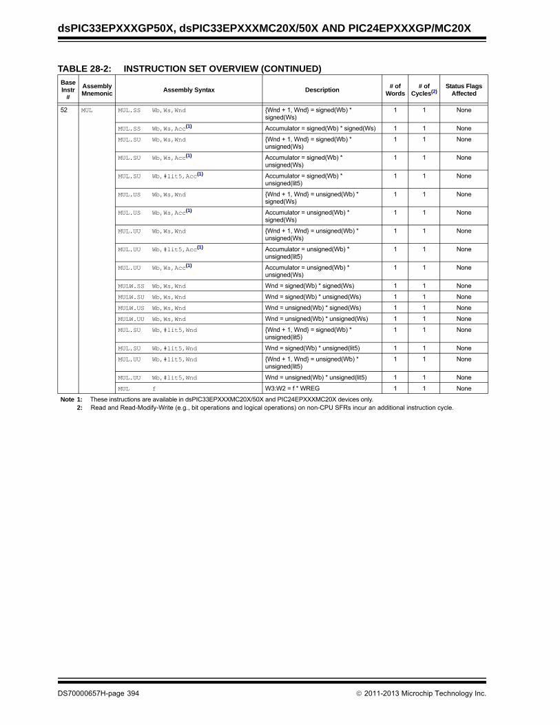
dsPIC33EPXXXGP50X, dsPIC33EPXXXMC20X/50X AND PIC24EPXXXGP/MC20X
52 MUL MUL.SS Wb,Ws,Wnd {Wnd + 1, Wnd} = signed(Wb) * signed(Ws)
1 1 None
MUL.SS Wb,Ws,Acc(1) Accumulator = signed(Wb) * signed(Ws) 1 1 None
MUL.SU Wb,Ws,Wnd {Wnd + 1, Wnd} = signed(Wb) * unsigned(Ws)
1 1 None
MUL.SU Wb,Ws,Acc(1) Accumulator = signed(Wb) * unsigned(Ws)
1 1 None
MUL.SU Wb,#lit5,Acc(1) Accumulator = signed(Wb) * unsigned(lit5)
1 1 None
MUL.US Wb,Ws,Wnd {Wnd + 1, Wnd} = unsigned(Wb) * signed(Ws)
1 1 None
MUL.US Wb,Ws,Acc(1) Accumulator = unsigned(Wb) * signed(Ws)
1 1 None
MUL.UU Wb,Ws,Wnd {Wnd + 1, Wnd} = unsigned(Wb) * unsigned(Ws)
1 1 None
MUL.UU Wb,#lit5,Acc(1) Accumulator = unsigned(Wb) * unsigned(lit5)
1 1 None
MUL.UU Wb,Ws,Acc(1) Accumulator = unsigned(Wb) * unsigned(Ws)
1 1 None
MULW.SS Wb,Ws,Wnd Wnd = signed(Wb) * signed(Ws) 1 1 None
MULW.SU Wb,Ws,Wnd Wnd = signed(Wb) * unsigned(Ws) 1 1 None
MULW.US Wb,Ws,Wnd Wnd = unsigned(Wb) * signed(Ws) 1 1 None
MULW.UU Wb,Ws,Wnd Wnd = unsigned(Wb) * unsigned(Ws) 1 1 None
MUL.SU Wb,#lit5,Wnd {Wnd + 1, Wnd} = signed(Wb) * unsigned(lit5)
1 1 None
MUL.SU Wb,#lit5,Wnd Wnd = signed(Wb) * unsigned(lit5) 1 1 None
MUL.UU Wb,#lit5,Wnd {Wnd + 1, Wnd} = unsigned(Wb) * unsigned(lit5)
1 1 None
MUL.UU Wb,#lit5,Wnd Wnd = unsigned(Wb) * unsigned(lit5) 1 1 None
MUL f W3:W2 = f * WREG 1 1 None
TABLE 28-2: INSTRUCTION SET OVERVIEW (CONTINUED)
BaseInstr
#
AssemblyMnemonic
Assembly Syntax Description# of
Words# of
Cycles(2)Status Flags
Affected
Note 1: These instructions are available in dsPIC33EPXXXMC20X/50X and PIC24EPXXXMC20X devices only.2: Read and Read-Modify-Write (e.g., bit operations and logical operations) on non-CPU SFRs incur an additional instruction cycle.
DS70000657H-page 394 2011-2013 Microchip Technology Inc.

dsPIC33EPXXXGP50X, dsPIC33EPXXXMC20X/50X AND PIC24EPXXXGP/MC20X
53 NEG NEG Acc(1) Negate Accumulator 1 1 OA,OB,OAB,SA,SB,SAB
NEG f f = f + 1 1 1 C,DC,N,OV,Z
NEG f,WREG WREG = f + 1 1 1 C,DC,N,OV,Z
NEG Ws,Wd Wd = Ws + 1 1 1 C,DC,N,OV,Z
54 NOP NOP No Operation 1 1 None
NOPR No Operation 1 1 None
55 POP POP f Pop f from Top-of-Stack (TOS) 1 1 None
POP Wdo Pop from Top-of-Stack (TOS) to Wdo 1 1 None
POP.D Wnd Pop from Top-of-Stack (TOS) to W(nd):W(nd + 1)
1 2 None
POP.S Pop Shadow Registers 1 1 All
56 PUSH PUSH f Push f to Top-of-Stack (TOS) 1 1 None
PUSH Wso Push Wso to Top-of-Stack (TOS) 1 1 None
PUSH.D Wns Push W(ns):W(ns + 1) to Top-of-Stack (TOS)
1 2 None
PUSH.S Push Shadow Registers 1 1 None
57 PWRSAV PWRSAV #lit1 Go into Sleep or Idle mode 1 1 WDTO,Sleep
58 RCALL RCALL Expr Relative Call 1 4 SFA
RCALL Wn Computed Call 1 4 SFA
59 REPEAT REPEAT #lit15 Repeat Next Instruction lit15 + 1 times 1 1 None
REPEAT Wn Repeat Next Instruction (Wn) + 1 times 1 1 None
60 RESET RESET Software device Reset 1 1 None
61 RETFIE RETFIE Return from interrupt 1 6 (5) SFA
62 RETLW RETLW #lit10,Wn Return with literal in Wn 1 6 (5) SFA
63 RETURN RETURN Return from Subroutine 1 6 (5) SFA
64 RLC RLC f f = Rotate Left through Carry f 1 1 C,N,Z
RLC f,WREG WREG = Rotate Left through Carry f 1 1 C,N,Z
RLC Ws,Wd Wd = Rotate Left through Carry Ws 1 1 C,N,Z
65 RLNC RLNC f f = Rotate Left (No Carry) f 1 1 N,Z
RLNC f,WREG WREG = Rotate Left (No Carry) f 1 1 N,Z
RLNC Ws,Wd Wd = Rotate Left (No Carry) Ws 1 1 N,Z
66 RRC RRC f f = Rotate Right through Carry f 1 1 C,N,Z
RRC f,WREG WREG = Rotate Right through Carry f 1 1 C,N,Z
RRC Ws,Wd Wd = Rotate Right through Carry Ws 1 1 C,N,Z
67 RRNC RRNC f f = Rotate Right (No Carry) f 1 1 N,Z
RRNC f,WREG WREG = Rotate Right (No Carry) f 1 1 N,Z
RRNC Ws,Wd Wd = Rotate Right (No Carry) Ws 1 1 N,Z
68 SAC SAC Acc,#Slit4,Wdo(1) Store Accumulator 1 1 None
SAC.R Acc,#Slit4,Wdo(1) Store Rounded Accumulator 1 1 None
69 SE SE Ws,Wnd Wnd = sign-extended Ws 1 1 C,N,Z
70 SETM SETM f f = 0xFFFF 1 1 None
SETM WREG WREG = 0xFFFF 1 1 None
SETM Ws Ws = 0xFFFF 1 1 None
71 SFTAC SFTAC Acc,Wn(1) Arithmetic Shift Accumulator by (Wn) 1 1 OA,OB,OAB,SA,SB,SAB
SFTAC Acc,#Slit6(1) Arithmetic Shift Accumulator by Slit6 1 1 OA,OB,OAB,SA,SB,SAB
TABLE 28-2: INSTRUCTION SET OVERVIEW (CONTINUED)
BaseInstr
#
AssemblyMnemonic
Assembly Syntax Description# of
Words# of
Cycles(2)Status Flags
Affected
Note 1: These instructions are available in dsPIC33EPXXXMC20X/50X and PIC24EPXXXMC20X devices only.2: Read and Read-Modify-Write (e.g., bit operations and logical operations) on non-CPU SFRs incur an additional instruction cycle.
2011-2013 Microchip Technology Inc. DS70000657H-page 395

dsPIC33EPXXXGP50X, dsPIC33EPXXXMC20X/50X AND PIC24EPXXXGP/MC20X
72 SL SL f f = Left Shift f 1 1 C,N,OV,Z
SL f,WREG WREG = Left Shift f 1 1 C,N,OV,Z
SL Ws,Wd Wd = Left Shift Ws 1 1 C,N,OV,Z
SL Wb,Wns,Wnd Wnd = Left Shift Wb by Wns 1 1 N,Z
SL Wb,#lit5,Wnd Wnd = Left Shift Wb by lit5 1 1 N,Z
73 SUB SUB Acc(1) Subtract Accumulators 1 1 OA,OB,OAB,SA,SB,SAB
SUB f f = f – WREG 1 1 C,DC,N,OV,Z
SUB f,WREG WREG = f – WREG 1 1 C,DC,N,OV,Z
SUB #lit10,Wn Wn = Wn – lit10 1 1 C,DC,N,OV,Z
SUB Wb,Ws,Wd Wd = Wb – Ws 1 1 C,DC,N,OV,Z
SUB Wb,#lit5,Wd Wd = Wb – lit5 1 1 C,DC,N,OV,Z
74 SUBB SUBB f f = f – WREG – (C) 1 1 C,DC,N,OV,Z
SUBB f,WREG WREG = f – WREG – (C) 1 1 C,DC,N,OV,Z
SUBB #lit10,Wn Wn = Wn – lit10 – (C) 1 1 C,DC,N,OV,Z
SUBB Wb,Ws,Wd Wd = Wb – Ws – (C) 1 1 C,DC,N,OV,Z
SUBB Wb,#lit5,Wd Wd = Wb – lit5 – (C) 1 1 C,DC,N,OV,Z
75 SUBR SUBR f f = WREG – f 1 1 C,DC,N,OV,Z
SUBR f,WREG WREG = WREG – f 1 1 C,DC,N,OV,Z
SUBR Wb,Ws,Wd Wd = Ws – Wb 1 1 C,DC,N,OV,Z
SUBR Wb,#lit5,Wd Wd = lit5 – Wb 1 1 C,DC,N,OV,Z
76 SUBBR SUBBR f f = WREG – f – (C) 1 1 C,DC,N,OV,Z
SUBBR f,WREG WREG = WREG – f – (C) 1 1 C,DC,N,OV,Z
SUBBR Wb,Ws,Wd Wd = Ws – Wb – (C) 1 1 C,DC,N,OV,Z
SUBBR Wb,#lit5,Wd Wd = lit5 – Wb – (C) 1 1 C,DC,N,OV,Z
77 SWAP SWAP.b Wn Wn = nibble swap Wn 1 1 None
SWAP Wn Wn = byte swap Wn 1 1 None
78 TBLRDH TBLRDH Ws,Wd Read Prog<23:16> to Wd<7:0> 1 5 None
79 TBLRDL TBLRDL Ws,Wd Read Prog<15:0> to Wd 1 5 None
80 TBLWTH TBLWTH Ws,Wd Write Ws<7:0> to Prog<23:16> 1 2 None
81 TBLWTL TBLWTL Ws,Wd Write Ws to Prog<15:0> 1 2 None
82 ULNK ULNK Unlink Frame Pointer 1 1 SFA
83 XOR XOR f f = f .XOR. WREG 1 1 N,Z
XOR f,WREG WREG = f .XOR. WREG 1 1 N,Z
XOR #lit10,Wn Wd = lit10 .XOR. Wd 1 1 N,Z
XOR Wb,Ws,Wd Wd = Wb .XOR. Ws 1 1 N,Z
XOR Wb,#lit5,Wd Wd = Wb .XOR. lit5 1 1 N,Z
84 ZE ZE Ws,Wnd Wnd = Zero-extend Ws 1 1 C,Z,N
TABLE 28-2: INSTRUCTION SET OVERVIEW (CONTINUED)
BaseInstr
#
AssemblyMnemonic
Assembly Syntax Description# of
Words# of
Cycles(2)Status Flags
Affected
Note 1: These instructions are available in dsPIC33EPXXXMC20X/50X and PIC24EPXXXMC20X devices only.2: Read and Read-Modify-Write (e.g., bit operations and logical operations) on non-CPU SFRs incur an additional instruction cycle.
DS70000657H-page 396 2011-2013 Microchip Technology Inc.

2011-2013 Microchip Technology Inc. DS70000657H-page 397
dsPIC33EPXXXGP50X, dsPIC33EPXXXMC20X/50X AND PIC24EPXXXGP/MC20X
29.0 DEVELOPMENT SUPPORT
The PIC® microcontrollers (MCU) and dsPIC® digitalsignal controllers (DSC) are supported with a full rangeof software and hardware development tools:
• Integrated Development Environment
- MPLAB® X IDE Software
• Compilers/Assemblers/Linkers
- MPLAB XC Compiler
- MPASMTM Assembler
- MPLINKTM Object Linker/MPLIBTM Object Librarian
- MPLAB Assembler/Linker/Librarian forVarious Device Families
• Simulators
- MPLAB X SIM Software Simulator
• Emulators
- MPLAB REAL ICE™ In-Circuit Emulator
• In-Circuit Debuggers/Programmers
- MPLAB ICD 3
- PICkit™ 3
• Device Programmers
- MPLAB PM3 Device Programmer
• Low-Cost Demonstration/Development Boards, Evaluation Kits and Starter Kits
• Third-party development tools
29.1 MPLAB X Integrated Development Environment Software
The MPLAB X IDE is a single, unified graphical userinterface for Microchip and third-party software, andhardware development tool that runs on Windows®,Linux and Mac OS® X. Based on the NetBeans IDE,MPLAB X IDE is an entirely new IDE with a host of freesoftware components and plug-ins for high-performance application development and debugging.Moving between tools and upgrading from softwaresimulators to hardware debugging and programmingtools is simple with the seamless user interface.
With complete project management, visual call graphs,a configurable watch window and a feature-rich editorthat includes code completion and context menus,MPLAB X IDE is flexible and friendly enough for newusers. With the ability to support multiple tools onmultiple projects with simultaneous debugging, MPLABX IDE is also suitable for the needs of experiencedusers.
Feature-Rich Editor:
• Color syntax highlighting
• Smart code completion makes suggestions and provides hints as you type
• Automatic code formatting based on user-defined rules
• Live parsing
User-Friendly, Customizable Interface:
• Fully customizable interface: toolbars, toolbar buttons, windows, window placement, etc.
• Call graph window
Project-Based Workspaces:
• Multiple projects
• Multiple tools
• Multiple configurations
• Simultaneous debugging sessions
File History and Bug Tracking:
• Local file history feature
• Built-in support for Bugzilla issue tracker

dsPIC33EPXXXGP50X, dsPIC33EPXXXMC20X/50X AND PIC24EPXXXGP/MC20X
DS70000657H-page 398 2011-2013 Microchip Technology Inc.
29.2 MPLAB XC Compilers
The MPLAB XC Compilers are complete ANSI Ccompilers for all of Microchip’s 8, 16 and 32-bit MCUand DSC devices. These compilers provide powerfulintegration capabilities, superior code optimization andease of use. MPLAB XC Compilers run on Windows,Linux or MAC OS X.
For easy source level debugging, the compilers providedebug information that is optimized to the MPLAB XIDE.
The free MPLAB XC Compiler editions support alldevices and commands, with no time or memoryrestrictions, and offer sufficient code optimization formost applications.
MPLAB XC Compilers include an assembler, linker andutilities. The assembler generates relocatable objectfiles that can then be archived or linked with otherrelocatable object files and archives to create an exe-cutable file. MPLAB XC Compiler uses the assemblerto produce its object file. Notable features of theassembler include:
• Support for the entire device instruction set
• Support for fixed-point and floating-point data
• Command-line interface
• Rich directive set
• Flexible macro language
• MPLAB X IDE compatibility
29.3 MPASM Assembler
The MPASM Assembler is a full-featured, universalmacro assembler for PIC10/12/16/18 MCUs.
The MPASM Assembler generates relocatable objectfiles for the MPLINK Object Linker, Intel® standard HEXfiles, MAP files to detail memory usage and symbolreference, absolute LST files that contain source linesand generated machine code, and COFF files fordebugging.
The MPASM Assembler features include:
• Integration into MPLAB X IDE projects
• User-defined macros to streamline assembly code
• Conditional assembly for multipurpose source files
• Directives that allow complete control over the assembly process
29.4 MPLINK Object Linker/MPLIB Object Librarian
The MPLINK Object Linker combines relocatableobjects created by the MPASM Assembler. It can linkrelocatable objects from precompiled libraries, usingdirectives from a linker script.
The MPLIB Object Librarian manages the creation andmodification of library files of precompiled code. Whena routine from a library is called from a source file, onlythe modules that contain that routine will be linked inwith the application. This allows large libraries to beused efficiently in many different applications.
The object linker/library features include:
• Efficient linking of single libraries instead of many smaller files
• Enhanced code maintainability by grouping related modules together
• Flexible creation of libraries with easy module listing, replacement, deletion and extraction
29.5 MPLAB Assembler, Linker and Librarian for Various Device Families
MPLAB Assembler produces relocatable machinecode from symbolic assembly language for PIC24,PIC32 and dsPIC DSC devices. MPLAB XC Compileruses the assembler to produce its object file. Theassembler generates relocatable object files that canthen be archived or linked with other relocatable objectfiles and archives to create an executable file. Notablefeatures of the assembler include:
• Support for the entire device instruction set
• Support for fixed-point and floating-point data
• Command-line interface
• Rich directive set
• Flexible macro language
• MPLAB X IDE compatibility
2011-2013 Microchip Technology Inc. DS70000657H-page 399
dsPIC33EPXXXGP50X, dsPIC33EPXXXMC20X/50X AND PIC24EPXXXGP/MC20X
29.6 MPLAB X SIM Software Simulator
The MPLAB X SIM Software Simulator allows codedevelopment in a PC-hosted environment by simulat-ing the PIC MCUs and dsPIC DSCs on an instructionlevel. On any given instruction, the data areas can beexamined or modified and stimuli can be applied froma comprehensive stimulus controller. Registers can belogged to files for further run-time analysis. The tracebuffer and logic analyzer display extend the power ofthe simulator to record and track program execution,actions on I/O, most peripherals and internal registers.
The MPLAB X SIM Software Simulator fully supportssymbolic debugging using the MPLAB XC Compilers,and the MPASM and MPLAB Assemblers. The soft-ware simulator offers the flexibility to develop anddebug code outside of the hardware laboratory envi-ronment, making it an excellent, economical softwaredevelopment tool.
29.7 MPLAB REAL ICE In-Circuit Emulator System
The MPLAB REAL ICE In-Circuit Emulator System isMicrochip’s next generation high-speed emulator forMicrochip Flash DSC and MCU devices. It debugs andprograms all 8, 16 and 32-bit MCU, and DSC deviceswith the easy-to-use, powerful graphical user interface ofthe MPLAB X IDE.
The emulator is connected to the design engineer’sPC using a high-speed USB 2.0 interface and isconnected to the target with either a connectorcompatible with in-circuit debugger systems (RJ-11)or with the new high-speed, noise tolerant, Low-Voltage Differential Signal (LVDS) interconnection(CAT5).
The emulator is field upgradable through future firmwaredownloads in MPLAB X IDE. MPLAB REAL ICE offerssignificant advantages over competitive emulatorsincluding full-speed emulation, run-time variablewatches, trace analysis, complex breakpoints, logicprobes, a ruggedized probe interface and long (up tothree meters) interconnection cables.
29.8 MPLAB ICD 3 In-Circuit Debugger System
The MPLAB ICD 3 In-Circuit Debugger System isMicrochip’s most cost-effective, high-speed hardwaredebugger/programmer for Microchip Flash DSC andMCU devices. It debugs and programs PIC Flashmicrocontrollers and dsPIC DSCs with the powerful,yet easy-to-use graphical user interface of the MPLABIDE.
The MPLAB ICD 3 In-Circuit Debugger probe isconnected to the design engineer’s PC using a high-speed USB 2.0 interface and is connected to the targetwith a connector compatible with the MPLAB ICD 2 orMPLAB REAL ICE systems (RJ-11). MPLAB ICD 3supports all MPLAB ICD 2 headers.
29.9 PICkit 3 In-Circuit Debugger/Programmer
The MPLAB PICkit 3 allows debugging and program-ming of PIC and dsPIC Flash microcontrollers at a mostaffordable price point using the powerful graphical userinterface of the MPLAB IDE. The MPLAB PICkit 3 isconnected to the design engineer’s PC using a full-speed USB interface and can be connected to thetarget via a Microchip debug (RJ-11) connector (com-patible with MPLAB ICD 3 and MPLAB REAL ICE). Theconnector uses two device I/O pins and the Reset lineto implement in-circuit debugging and In-Circuit SerialProgramming™ (ICSP™).
29.10 MPLAB PM3 Device Programmer
The MPLAB PM3 Device Programmer is a universal,CE compliant device programmer with programmablevoltage verification at VDDMIN and VDDMAX formaximum reliability. It features a large LCD display(128 x 64) for menus and error messages, and a mod-ular, detachable socket assembly to support variouspackage types. The ICSP cable assembly is includedas a standard item. In Stand-Alone mode, the MPLABPM3 Device Programmer can read, verify and programPIC devices without a PC connection. It can also setcode protection in this mode. The MPLAB PM3connects to the host PC via an RS-232 or USB cable.The MPLAB PM3 has high-speed communications andoptimized algorithms for quick programming of largememory devices, and incorporates an MMC card for filestorage and data applications.

dsPIC33EPXXXGP50X, dsPIC33EPXXXMC20X/50X AND PIC24EPXXXGP/MC20X
DS70000657H-page 400 2011-2013 Microchip Technology Inc.
29.11 Demonstration/Development Boards, Evaluation Kits and Starter Kits
A wide variety of demonstration, development andevaluation boards for various PIC MCUs and dsPICDSCs allows quick application development on fullyfunctional systems. Most boards include prototypingareas for adding custom circuitry and provide applica-tion firmware and source code for examination andmodification.
The boards support a variety of features, including LEDs,temperature sensors, switches, speakers, RS-232interfaces, LCD displays, potentiometers and additionalEEPROM memory.
The demonstration and development boards can beused in teaching environments, for prototyping customcircuits and for learning about various microcontrollerapplications.
In addition to the PICDEM™ and dsPICDEM™demonstration/development board series of circuits,Microchip has a line of evaluation kits and demonstra-tion software for analog filter design, KEELOQ® securityICs, CAN, IrDA®, PowerSmart battery management,SEEVAL® evaluation system, Sigma-Delta ADC, flowrate sensing, plus many more.
Also available are starter kits that contain everythingneeded to experience the specified device. This usuallyincludes a single application and debug capability, allon one board.
Check the Microchip web page (www.microchip.com)for the complete list of demonstration, developmentand evaluation kits.
29.12 Third-Party Development Tools
Microchip also offers a great collection of tools fromthird-party vendors. These tools are carefully selectedto offer good value and unique functionality.
• Device Programmers and Gang Programmers from companies, such as SoftLog and CCS
• Software Tools from companies, such as Gimpel and Trace Systems
• Protocol Analyzers from companies, such as Saleae and Total Phase
• Demonstration Boards from companies, such as MikroElektronika, Digilent® and Olimex
• Embedded Ethernet Solutions from companies, such as EZ Web Lynx, WIZnet and IPLogika®
dsPIC33EPXXXGP50X, dsPIC33EPXXXMC20X/50X AND PIC24EPXXXGP/MC20X
30.0 ELECTRICAL CHARACTERISTICS
This section provides an overview of dsPIC33EPXXXGP50X, dsPIC33EPXXXMC20X/50X and PIC24EPXXXGP/MC20X electrical characteristics. Additional information will be provided in future revisions of this document as itbecomes available.
Absolute maximum ratings for the dsPIC33EPXXXGP50X, dsPIC33EPXXXMC20X/50X and PIC24EPXXXGP/MC20Xfamily are listed below. Exposure to these maximum rating conditions for extended periods may affect device reliability.Functional operation of the device at these or any other conditions above the parameters indicated in the operationlistings of this specification is not implied.
Absolute Maximum Ratings(1)
Ambient temperature under bias............................................................................................................ .-40°C to +125°C
Storage temperature .............................................................................................................................. -65°C to +150°C
Voltage on VDD with respect to VSS .......................................................................................................... -0.3V to +4.0V
Voltage on any pin that is not 5V tolerant, with respect to VSS(3).................................................... -0.3V to (VDD + 0.3V)
Voltage on any 5V tolerant pin with respect to VSS when VDD 3.0V(3)................................................... -0.3V to +5.5V
Voltage on any 5V tolerant pin with respect to Vss when VDD < 3.0V(3)................................................... -0.3V to +3.6V
Maximum current out of VSS pin ...........................................................................................................................300 mA
Maximum current into VDD pin(2)...........................................................................................................................300 mA
Maximum current sunk/sourced by any 4x I/O pin..................................................................................................15 mA
Maximum current sunk/sourced by any 8x I/O pin ..................................................................................................25 mA
Maximum current sunk by all ports(2,4) .................................................................................................................200 mA
Note 1: Stresses above those listed under “Absolute Maximum Ratings” may cause permanent damage to thedevice. This is a stress rating only, and functional operation of the device at those or any other conditionsabove those indicated in the operation listings of this specification is not implied. Exposure to maximumrating conditions for extended periods may affect device reliability.
2: Maximum allowable current is a function of device maximum power dissipation (see Table 30-2).
3: See the “Pin Diagrams” section for the 5V tolerant pins.
4: Exceptions are: dsPIC33EPXXXGP502, dsPIC33EPXXXMC202/502 and PIC24EPXXXGP/MC202 devices,which have a maximum sink/source capability of 130 mA.
2011-2013 Microchip Technology Inc. DS70000657H-page 401

dsPIC33EPXXXGP50X, dsPIC33EPXXXMC20X/50X AND PIC24EPXXXGP/MC20X
30.1 DC Characteristics
TABLE 30-1: OPERATING MIPS VS. VOLTAGE
CharacteristicVDD Range(in Volts)
Temp Range(in °C)
Maximum MIPS
dsPIC33EPXXXGP50X, dsPIC33EPXXXMC20X/50X and
PIC24EPXXXGP/MC20X
— 3.0V to 3.6V(1) -40°C to +85°C 70
— 3.0V to 3.6V(1) -40°C to +125°C 60
Note 1: Device is functional at VBORMIN < VDD < VDDMIN. Analog modules (ADC, op amp/comparator and comparator voltage reference) may have degraded performance. Device functionality is tested but not characterized. Refer to Parameter BO10 in Table 30-13 for the minimum and maximum BOR values.
TABLE 30-2: THERMAL OPERATING CONDITIONS
Rating Symbol Min. Typ. Max. Unit
Industrial Temperature Devices
Operating Junction Temperature Range TJ -40 — +125 °C
Operating Ambient Temperature Range TA -40 — +85 °C
Extended Temperature Devices
Operating Junction Temperature Range TJ -40 — +140 °C
Operating Ambient Temperature Range TA -40 — +125 °C
Power Dissipation:Internal chip power dissipation:
PINT = VDD x (IDD – IOH) PD PINT + PI/O WI/O Pin Power Dissipation:
I/O = ({VDD – VOH} x IOH) + (VOL x IOL)
Maximum Allowed Power Dissipation PDMAX (TJ – TA)/JA W
TABLE 30-3: THERMAL PACKAGING CHARACTERISTICS
Characteristic Symbol Typ. Max. Unit Notes
Package Thermal Resistance, 64-Pin QFN JA 28.0 — °C/W 1
Package Thermal Resistance, 64-Pin TQFP 10x10 mm JA 48.3 — °C/W 1
Package Thermal Resistance, 48-Pin UQFN 6x6 mm JA 41 — °C/W 1
Package Thermal Resistance, 44-Pin QFN JA 29.0 — °C/W 1
Package Thermal Resistance, 44-Pin TQFP 10x10 mm JA 49.8 — °C/W 1
Package Thermal Resistance, 44-Pin VTLA 6x6 mm JA 25.2 — °C/W 1
Package Thermal Resistance, 36-Pin VTLA 5x5 mm JA 28.5 — °C/W 1
Package Thermal Resistance, 28-Pin QFN-S JA 30.0 — °C/W 1
Package Thermal Resistance, 28-Pin SSOP JA 71.0 — °C/W 1
Package Thermal Resistance, 28-Pin SOIC JA 69.7 — °C/W 1
Package Thermal Resistance, 28-Pin SPDIP JA 60.0 — °C/W 1
Note 1: Junction to ambient thermal resistance, Theta-JA (JA) numbers are achieved by package simulations.
DS70000657H-page 402 2011-2013 Microchip Technology Inc.

dsPIC33EPXXXGP50X, dsPIC33EPXXXMC20X/50X AND PIC24EPXXXGP/MC20X
TABLE 30-5: FILTER CAPACITOR (CEFC) SPECIFICATIONS
TABLE 30-4: DC TEMPERATURE AND VOLTAGE SPECIFICATIONS
DC CHARACTERISTICS
Standard Operating Conditions (see Note 1): 3.0V to 3.6V(unless otherwise stated)Operating temperature -40°C TA +85°C for Industrial
-40°C TA +125°C for Extended
Param No.
Symbol Characteristic Min. Typ. Max. Units Conditions
Operating Voltage
DC10 VDD Supply Voltage 3.0 — 3.6 V
DC16 VPOR VDD Start Voltageto Ensure Internal Power-on Reset Signal
— — VSS V
DC17 SVDD VDD Rise Rateto Ensure InternalPower-on Reset Signal
0.03 — — V/ms 0V-1V in 100 ms
Note 1: Device is functional at VBORMIN < VDD < VDDMIN. Analog modules (ADC, op amp/comparator and comparator voltage reference) may have degraded performance. Device functionality is tested but not characterized. Refer to Parameter BO10 in Table 30-13 for the minimum and maximum BOR values.
Standard Operating Conditions (unless otherwise stated):Operating temperature -40°C TA +85°C for Industrial
-40°C TA +125°C for Extended
ParamNo.
Symbol Characteristics Min. Typ. Max. Units Comments
CEFC External Filter Capacitor Value(1)
4.7 10 — F Capacitor must have a low series resistance (< 1 Ohm)
Note 1: Typical VCAP voltage = 1.8 volts when VDD VDDMIN.
2011-2013 Microchip Technology Inc. DS70000657H-page 403

dsPIC33EPXXXGP50X, dsPIC33EPXXXMC20X/50X AND PIC24EPXXXGP/MC20X
TABLE 30-6: DC CHARACTERISTICS: OPERATING CURRENT (IDD)
DC CHARACTERISTICS
Standard Operating Conditions: 3.0V to 3.6V(unless otherwise stated)Operating temperature -40°C TA +85°C for Industrial
-40°C TA +125°C for Extended
Parameter No.
Typ. Max. Units Conditions
Operating Current (IDD)(1)
DC20d 9 15 mA -40°C
3.3V 10 MIPSDC20a 9 15 mA +25°C
DC20b 9 15 mA +85°C
DC20c 9 15 mA +125°C
DC22d 16 25 mA -40°C
3.3V 20 MIPSDC22a 16 25 mA +25°C
DC22b 16 25 mA +85°C
DC22c 16 25 mA +125°C
DC24d 27 40 mA -40°C
3.3V 40 MIPSDC24a 27 40 mA +25°C
DC24b 27 40 mA +85°C
DC24c 27 40 mA +125°C
DC25d 36 55 mA -40°C
3.3V 60 MIPSDC25a 36 55 mA +25°C
DC25b 36 55 mA +85°C
DC25c 36 55 mA +125°C
DC26d 41 60 mA -40°C
3.3V 70 MIPSDC26a 41 60 mA +25°C
DC26b 41 60 mA +85°C
Note 1: IDD is primarily a function of the operating voltage and frequency. Other factors, such as I/O pin loading and switching rate, oscillator type, internal code execution pattern and temperature, also have an impact on the current consumption. The test conditions for all IDD measurements are as follows:
• Oscillator is configured in EC mode with PLL, OSC1 is driven with external square wave from rail-to-rail (EC clock overshoot/undershoot < 250 mV required)
• CLKO is configured as an I/O input pin in the Configuration Word
• All I/O pins are configured as inputs and pulled to VSS
• MCLR = VDD, WDT and FSCM are disabled
• CPU, SRAM, program memory and data memory are operational
• No peripheral modules are operating; however, every peripheral is being clocked (all PMDx bits are zeroed)
• CPU is executing while(1){NOP();} statement
• JTAG is disabled
DS70000657H-page 404 2011-2013 Microchip Technology Inc.

dsPIC33EPXXXGP50X, dsPIC33EPXXXMC20X/50X AND PIC24EPXXXGP/MC20X
TABLE 30-7: DC CHARACTERISTICS: IDLE CURRENT (IIDLE)
DC CHARACTERISTICS
Standard Operating Conditions: 3.0V to 3.6V(unless otherwise stated)Operating temperature -40°C TA +85°C for Industrial
-40°C TA +125°C for Extended
Parameter No.
Typ. Max. Units Conditions
Idle Current (IIDLE)(1)
DC40d 3 8 mA -40°C
3.3V 10 MIPSDC40a 3 8 mA +25°C
DC40b 3 8 mA +85°C
DC40c 3 8 mA +125°C
DC42d 6 12 mA -40°C
3.3V 20 MIPSDC42a 6 12 mA +25°C
DC42b 6 12 mA +85°C
DC42c 6 12 mA +125°C
DC44d 11 18 mA -40°C
3.3V 40 MIPSDC44a 11 18 mA +25°C
18DC44b 11 mA +85°C
18DC44c 11 mA +125°C
DC45d 17 27 mA -40°C
3.3V 60 MIPSDC45a 17 27 mA +25°C
27DC45b 17 mA +85°C
27DC45c 17 mA +125°C
DC46d 20 35 mA -40°C
3.3V 70 MIPSDC46a 20 35 mA +25°C
35DC46b 20 mA +85°C
Note 1: Base Idle current (IIDLE) is measured as follows:
• CPU core is off, oscillator is configured in EC mode and external clock is active; OSC1 is driven with external square wave from rail-to-rail (EC clock overshoot/undershoot < 250 mV required)
• CLKO is configured as an I/O input pin in the Configuration Word
• All I/O pins are configured as inputs and pulled to VSS
• MCLR = VDD, WDT and FSCM are disabled
• No peripheral modules are operating; however, every peripheral is being clocked (all PMDx bits are zeroed)
• The NVMSIDL bit (NVMCON<12>) = 1 (i.e., Flash regulator is set to standby while the device is in Idle mode)
• The VREGSF bit (RCON<11>) = 0 (i.e., Flash regulator is set to standby while the device is in Sleep mode)
• JTAG is disabled
2011-2013 Microchip Technology Inc. DS70000657H-page 405

dsPIC33EPXXXGP50X, dsPIC33EPXXXMC20X/50X AND PIC24EPXXXGP/MC20X
TABLE 30-8: DC CHARACTERISTICS: POWER-DOWN CURRENT (IPD)
DC CHARACTERISTICS
Standard Operating Conditions: 3.0V to 3.6V(unless otherwise stated)Operating temperature -40°C TA +85°C for Industrial
-40°C TA +125°C for Extended
Parameter No.
Typ. Max. Units Conditions
Power-Down Current (IPD)(1) – dsPIC33EP32GP50X, dsPIC33EP32MC20X/50X and PIC24EP32GP/MC20X
DC60d 30 100 A -40°C
3.3VDC60a 35 100 A +25°C
DC60b 150 200 A +85°C
DC60c 250 500 A +125°C
Power-Down Current (IPD)(1) – dsPIC33EP64GP50X, dsPIC33EP64MC20X/50X and PIC24EP64GP/MC20X
DC60d 25 100 A -40°C
3.3VDC60a 30 100 A +25°C
DC60b 150 350 A +85°C
DC60c 350 800 A +125°C
Power-Down Current (IPD)(1) – dsPIC33EP128GP50X, dsPIC33EP128MC20X/50X and PIC24EP128GP/MC20X
DC60d 30 100 A -40°C
3.3VDC60a 35 100 A +25°C
DC60b 150 350 A +85°C
DC60c 550 1000 A +125°C
Power-Down Current (IPD)(1) – dsPIC33EP256GP50X, dsPIC33EP256MC20X/50X and PIC24EP256GP/MC20X
DC60d 35 100 A -40°C
3.3VDC60a 40 100 A +25°C
DC60b 250 450 A +85°C
DC60c 1000 1200 A +125°C
Power-Down Current (IPD)(1) – dsPIC33EP512GP50X, dsPIC33EP512MC20X/50X and PIC24EP512GP/MC20X
DC60d 40 100 A -40°C
3.3VDC60a 45 100 A +25°C
DC60b 350 800 A +85°C
DC60c 1100 1500 A +125°C
Note 1: IPD (Sleep) current is measured as follows:• CPU core is off, oscillator is configured in EC mode and external clock is active; OSC1 is driven with
external square wave from rail-to-rail (EC clock overshoot/undershoot < 250 mV required)• CLKO is configured as an I/O input pin in the Configuration Word• All I/O pins are configured as inputs and pulled to VSS
• MCLR = VDD, WDT and FSCM are disabled• All peripheral modules are disabled (PMDx bits are all set)• The VREGS bit (RCON<8>) = 0 (i.e., core regulator is set to standby while the device is in Sleep
mode)• The VREGSF bit (RCON<11>) = 0 (i.e., Flash regulator is set to standby while the device is in Sleep
mode)• JTAG is disabled
DS70000657H-page 406 2011-2013 Microchip Technology Inc.

dsPIC33EPXXXGP50X, dsPIC33EPXXXMC20X/50X AND PIC24EPXXXGP/MC20X
TABLE 30-9: DC CHARACTERISTICS: WATCHDOG TIMER DELTA CURRENT (IWDT)(1)
DC CHARACTERISTICS
Standard Operating Conditions: 3.0V to 3.6V(unless otherwise stated)Operating temperature -40°C TA +85°C for Industrial
-40°C TA +125°C for Extended
Parameter No. Typ. Max. Units Conditions
DC61d 8 — A -40°C
3.3VDC61a 10 — A +25°C
DC61b 12 — A +85°C
DC61c 13 — A +125°C
Note 1: The IWDT current is the additional current consumed when the module is enabled. This current should be added to the base IPD current. All parameters are characterized but not tested during manufacturing.
TABLE 30-10: DC CHARACTERISTICS: DOZE CURRENT (IDOZE)
DC CHARACTERISTICS
Standard Operating Conditions: 3.0V to 3.6V(unless otherwise stated)Operating temperature -40°C TA +85°C for Industrial
-40°C TA +125°C for Extended
Parameter No. Typ. Max.Doze Ratio
Units Conditions
Doze Current (IDOZE)(1)
DC73a(2) 35 — 1:2 mA-40°C 3.3V FOSC = 140 MHz
DC73g 20 30 1:128 mA
DC70a(2) 35 — 1:2 mA+25°C 3.3V FOSC = 140 MHz
DC70g 20 30 1:128 mA
DC71a(2) 35 — 1:2 mA+85°C 3.3V FOSC = 140 MHz
DC71g 20 30 1:128 mA
DC72a(2) 28 — 1:2 mA+125°C 3.3V FOSC = 120 MHz
DC72g 15 30 1:128 mA
Note 1: IDOZE is primarily a function of the operating voltage and frequency. Other factors, such as I/O pin loading and switching rate, oscillator type, internal code execution pattern and temperature, also have an impact on the current consumption. The test conditions for all IDOZE measurements are as follows:
• Oscillator is configured in EC mode and external clock is active, OSC1 is driven with external square wave from rail-to-rail (EC clock overshoot/undershoot < 250 mV required)
• CLKO is configured as an I/O input pin in the Configuration Word
• All I/O pins are configured as inputs and pulled to VSS
• MCLR = VDD, WDT and FSCM are disabled
• CPU, SRAM, program memory and data memory are operational
• No peripheral modules are operating; however, every peripheral is being clocked (all PMDx bits are zeroed)
• CPU is executing while(1) statement
• JTAG is disabled
2: Parameter is characterized but not tested in manufacturing.
2011-2013 Microchip Technology Inc. DS70000657H-page 407

dsPIC33EPXXXGP50X, dsPIC33EPXXXMC20X/50X AND PIC24EPXXXGP/MC20X
TABLE 30-11: DC CHARACTERISTICS: I/O PIN INPUT SPECIFICATIONS
DC CHARACTERISTICS
Standard Operating Conditions: 3.0V to 3.6V(unless otherwise stated)Operating temperature -40°C TA +85°C for Industrial
-40°C TA +125°C for Extended
Param No.
Symbol Characteristic Min. Typ. Max. Units Conditions
VIL Input Low Voltage
DI10 Any I/O Pin and MCLR VSS — 0.2 VDD V
DI18 I/O Pins with SDAx, SCLx VSS — 0.3 VDD V SMBus disabled
DI19 I/O Pins with SDAx, SCLx VSS — 0.8 V SMBus enabled
VIH Input High Voltage
DI20 I/O Pins Not 5V Tolerant 0.8 VDD — VDD V (Note 3)
I/O Pins 5V Tolerant and MCLR
0.8 VDD — 5.5 V (Note 3)
I/O Pins with SDAx, SCLx 0.8 VDD — 5.5 V SMBus disabled
I/O Pins with SDAx, SCLx 2.1 — 5.5 V SMBus enabled
ICNPU Change Notification Pull-up Current
DI30 150 250 550 A VDD = 3.3V, VPIN = VSS
ICNPD Change Notification Pull-Down Current(4)
DI31 20 50 100 A VDD = 3.3V, VPIN = VDD
Note 1: The leakage current on the MCLR pin is strongly dependent on the applied voltage level. The specified levels represent normal operating conditions. Higher leakage current can be measured at different input voltages.
2: Negative current is defined as current sourced by the pin.
3: See the “Pin Diagrams” section for the 5V tolerant I/O pins.
4: VIL source < (VSS – 0.3). Characterized but not tested.
5: Non-5V tolerant pins VIH source > (VDD + 0.3), 5V tolerant pins VIH source > 5.5V. Characterized but not tested.
6: Digital 5V tolerant pins cannot tolerate any “positive” input injection current from input sources > 5.5V.
7: Non-zero injection currents can affect the ADC results by approximately 4-6 counts.
8: Any number and/or combination of I/O pins not excluded under IICL or IICH conditions are permitted provided the mathematical “absolute instantaneous” sum of the input injection currents from all pins do not exceed the specified limit. Characterized but not tested.
DS70000657H-page 408 2011-2013 Microchip Technology Inc.

dsPIC33EPXXXGP50X, dsPIC33EPXXXMC20X/50X AND PIC24EPXXXGP/MC20X
IIL Input Leakage Current(1,2)
DI50 I/O Pins 5V Tolerant(3) -1 — +1 A VSS VPIN VDD,Pin at high-impedance
DI51 I/O Pins Not 5V Tolerant(3) -1 — +1 A VSS VPIN VDD, Pin at high-impedance, -40°C TA +85°C
DI51a I/O Pins Not 5V Tolerant(3) -1 — +1 A Analog pins shared with external reference pins, -40°C TA +85°C
DI51b I/O Pins Not 5V Tolerant(3) -1 — +1 A VSS VPIN VDD, Pin at high-impedance, -40°C TA +125°C
DI51c I/O Pins Not 5V Tolerant(3) -1 — +1 A Analog pins shared with external reference pins, -40°C TA +125°C
DI55 MCLR -5 — +5 A VSS VPIN VDD
DI56 OSC1 -5 — +5 A VSS VPIN VDD,XT and HS modes
TABLE 30-11: DC CHARACTERISTICS: I/O PIN INPUT SPECIFICATIONS (CONTINUED)
DC CHARACTERISTICS
Standard Operating Conditions: 3.0V to 3.6V(unless otherwise stated)Operating temperature -40°C TA +85°C for Industrial
-40°C TA +125°C for Extended
Param No.
Symbol Characteristic Min. Typ. Max. Units Conditions
Note 1: The leakage current on the MCLR pin is strongly dependent on the applied voltage level. The specified levels represent normal operating conditions. Higher leakage current can be measured at different input voltages.
2: Negative current is defined as current sourced by the pin.
3: See the “Pin Diagrams” section for the 5V tolerant I/O pins.
4: VIL source < (VSS – 0.3). Characterized but not tested.
5: Non-5V tolerant pins VIH source > (VDD + 0.3), 5V tolerant pins VIH source > 5.5V. Characterized but not tested.
6: Digital 5V tolerant pins cannot tolerate any “positive” input injection current from input sources > 5.5V.
7: Non-zero injection currents can affect the ADC results by approximately 4-6 counts.
8: Any number and/or combination of I/O pins not excluded under IICL or IICH conditions are permitted provided the mathematical “absolute instantaneous” sum of the input injection currents from all pins do not exceed the specified limit. Characterized but not tested.
2011-2013 Microchip Technology Inc. DS70000657H-page 409

dsPIC33EPXXXGP50X, dsPIC33EPXXXMC20X/50X AND PIC24EPXXXGP/MC20X
IICL Input Low Injection Current
DI60a 0 — -5(4,7) mA All pins except VDD, VSS, AVDD, AVSS, MCLR, VCAP and RB7
IICH Input High Injection Current
DI60b 0 — +5(5,6,7) mA All pins except VDD, VSS, AVDD, AVSS, MCLR, VCAP, RB7 and all 5V tolerant pins(6)
IICT Total Input Injection Current
DI60c (sum of all I/O and control pins)
-20(8) — +20(8) mA Absolute instantaneous sum of all ± input injection cur-rents from all I/O pins( | IICL + | IICH | ) IICT
TABLE 30-11: DC CHARACTERISTICS: I/O PIN INPUT SPECIFICATIONS (CONTINUED)
DC CHARACTERISTICS
Standard Operating Conditions: 3.0V to 3.6V(unless otherwise stated)Operating temperature -40°C TA +85°C for Industrial
-40°C TA +125°C for Extended
Param No.
Symbol Characteristic Min. Typ. Max. Units Conditions
Note 1: The leakage current on the MCLR pin is strongly dependent on the applied voltage level. The specified levels represent normal operating conditions. Higher leakage current can be measured at different input voltages.
2: Negative current is defined as current sourced by the pin.
3: See the “Pin Diagrams” section for the 5V tolerant I/O pins.
4: VIL source < (VSS – 0.3). Characterized but not tested.
5: Non-5V tolerant pins VIH source > (VDD + 0.3), 5V tolerant pins VIH source > 5.5V. Characterized but not tested.
6: Digital 5V tolerant pins cannot tolerate any “positive” input injection current from input sources > 5.5V.
7: Non-zero injection currents can affect the ADC results by approximately 4-6 counts.
8: Any number and/or combination of I/O pins not excluded under IICL or IICH conditions are permitted provided the mathematical “absolute instantaneous” sum of the input injection currents from all pins do not exceed the specified limit. Characterized but not tested.
DS70000657H-page 410 2011-2013 Microchip Technology Inc.

dsPIC33EPXXXGP50X, dsPIC33EPXXXMC20X/50X AND PIC24EPXXXGP/MC20X
TABLE 30-12: DC CHARACTERISTICS: I/O PIN OUTPUT SPECIFICATIONS
DC CHARACTERISTICS
Standard Operating Conditions: 3.0V to 3.6V(unless otherwise stated)Operating temperature -40°C TA +85°C for Industrial
-40°C TA +125°C for Extended
Param. Symbol Characteristic Min. Typ. Max. Units Conditions
DO10 VOL Output Low Voltage4x Sink Driver Pins(2)
— — 0.4 V VDD = 3.3V,IOL 6 mA, -40°C TA +85°CIOL 5 mA, +85°C TA +125°C
Output Low Voltage8x Sink Driver Pins(3)
— — 0.4 V VDD = 3.3V,IOL 12 mA, -40°C TA +85°CIOL 8 mA, +85°C TA +125°C
DO20 VOH Output High Voltage4x Source Driver Pins(2)
2.4 — — V IOH -10 mA, VDD = 3.3V
Output High Voltage8x Source Driver Pins(3)
2.4 — — V IOH -15 mA, VDD = 3.3V
DO20A VOH1 Output High Voltage4x Source Driver Pins(2)
1.5(1) — — V IOH -14 mA, VDD = 3.3V
2.0(1) — — IOH -12 mA, VDD = 3.3V
3.0(1) — — IOH -7 mA, VDD = 3.3V
Output High Voltage8x Source Driver Pins(3)
1.5(1) — — V IOH -22 mA, VDD = 3.3V
2.0(1) — — IOH -18 mA, VDD = 3.3V
3.0(1) — — IOH -10 mA, VDD = 3.3V
Note 1: Parameters are characterized but not tested.
2: Includes all I/O pins that are not 8x Sink Driver pins (see below).
3: Includes the following pins:For devices with less than 64 pins: RA3, RA4, RA9, RB<7:15> and RC3For 64-pin devices: RA4, RA9, RB<7:15>, RC3 and RC15
TABLE 30-13: ELECTRICAL CHARACTERISTICS: BOR
DC CHARACTERISTICS
Standard Operating Conditions: 3.0V to 3.6V(unless otherwise stated)(1)
Operating temperature -40°C TA +85°C for Industrial-40°C TA +125°C for Extended
ParamNo.
Symbol Characteristic Min.(2) Typ. Max. Units Conditions
BO10 VBOR BOR Event on VDD Transition High-to-Low
2.65 — 2.95 V VDD
(Notes 2 and 3)
Note 1: Device is functional at VBORMIN < VDD < VDDMIN, but will have degraded performance. Device functionality is tested, but not characterized. Analog modules (ADC, op amp/comparator and comparator voltage reference) may have degraded performance.
2: Parameters are for design guidance only and are not tested in manufacturing.
3: The VBOR specification is relative to VDD.
2011-2013 Microchip Technology Inc. DS70000657H-page 411

dsPIC33EPXXXGP50X, dsPIC33EPXXXMC20X/50X AND PIC24EPXXXGP/MC20X
TABLE 30-14: DC CHARACTERISTICS: PROGRAM MEMORY
DC CHARACTERISTICS
Standard Operating Conditions: 3.0V to 3.6V(unless otherwise stated)Operating temperature -40°C TA +85°C for Industrial
-40°C TA +125°C for Extended
ParamNo.
Symbol Characteristic Min. Typ.(1) Max. Units Conditions
Program Flash Memory
D130 EP Cell Endurance 10,000 — — E/W -40C to +125C
D131 VPR VDD for Read 3.0 — 3.6 V
D132b VPEW VDD for Self-Timed Write 3.0 — 3.6 V
D134 TRETD Characteristic Retention 20 — — Year Provided no other specifications are violated, -40C to +125C
D135 IDDP Supply Current during Programming(2)
— 10 — mA
D136 IPEAK Instantaneous Peak Current During Start-up
— — 150 mA
D137a TPE Page Erase Time 17.7 — 22.9 ms TPE = 146893 FRC cycles, TA = +85°C (See Note 3)
D137b TPE Page Erase Time 17.5 — 23.1 ms TPE = 146893 FRC cycles, TA = +125°C (See Note 3)
D138a TWW Word Write Cycle Time 41.7 — 53.8 µs TWW = 346 FRC cycles, TA = +85°C (See Note 3)
D138b TWW Word Write Cycle Time 41.2 — 54.4 µs TWW = 346 FRC cycles, TA = +125°C (See Note 3)
Note 1: Data in “Typical” column is at 3.3V, +25°C unless otherwise stated.
2: Parameter characterized but not tested in manufacturing.
3: Other conditions: FRC = 7.37 MHz, TUN<5:0> = 011111 (for Minimum), TUN<5:0> = 100000 (for Maximum). This parameter depends on the FRC accuracy (see Table 30-19) and the value of the FRC Oscillator Tuning register (see Register 9-4). For complete details on calculating the Minimum and Maximum time, see Section 5.3 “Programming Operations”.
DS70000657H-page 412 2011-2013 Microchip Technology Inc.

dsPIC33EPXXXGP50X, dsPIC33EPXXXMC20X/50X AND PIC24EPXXXGP/MC20X
30.2 AC Characteristics and Timing Parameters
This section defines dsPIC33EPXXXGP50X,dsPIC33EPXXXMC20X/50X and PIC24EPXXXGP/MC20X AC characteristics and timing parameters.
TABLE 30-15: TEMPERATURE AND VOLTAGE SPECIFICATIONS – AC
FIGURE 30-1: LOAD CONDITIONS FOR DEVICE TIMING SPECIFICATIONS
TABLE 30-16: CAPACITIVE LOADING REQUIREMENTS ON OUTPUT PINS
AC CHARACTERISTICS
Standard Operating Conditions: 3.0V to 3.6V(unless otherwise stated)Operating temperature -40°C TA +85°C for Industrial
-40°C TA +125°C for ExtendedOperating voltage VDD range as described in Section 30.1 “DC Characteristics”.
Param No.
Symbol Characteristic Min. Typ. Max. Units Conditions
DO50 COSCO OSC2 Pin — — 15 pF In XT and HS modes, when external clock is used to drive OSC1
DO56 CIO All I/O Pins and OSC2 — — 50 pF EC mode
DO58 CB SCLx, SDAx — — 400 pF In I2C™ mode
VDD/2
CL
RL
Pin
Pin
VSS
VSS
CL
RL = 464CL = 50 pF for all pins except OSC2
15 pF for OSC2 output
Load Condition 1 – for all pins except OSC2 Load Condition 2 – for OSC2
2011-2013 Microchip Technology Inc. DS70000657H-page 413

dsPIC33EPXXXGP50X, dsPIC33EPXXXMC20X/50X AND PIC24EPXXXGP/MC20X
FIGURE 30-2: EXTERNAL CLOCK TIMING
Q1 Q2 Q3 Q4
OSC1
CLKO
Q1 Q2 Q3
OS20OS30 OS30
OS40OS41
OS31 OS31
Q4
OS25
TABLE 30-17: EXTERNAL CLOCK TIMING REQUIREMENTS
AC CHARACTERISTICS
Standard Operating Conditions: 3.0V to 3.6V(unless otherwise stated)Operating temperature -40°C TA +85°C for Industrial
-40°C TA +125°C for Extended
ParamNo.
Symb Characteristic Min. Typ.(1) Max. Units Conditions
OS10 FIN External CLKI Frequency(External clocks allowed onlyin EC and ECPLL modes)
DC — 60 MHz EC
Oscillator Crystal Frequency 3.510
——
1025
MHzMHz
XTHS
OS20 TOSC TOSC = 1/FOSC 8.33 — DC ns +125ºC
TOSC = 1/FOSC 7.14 — DC ns +85ºC
OS25 TCY Instruction Cycle Time(2) 16.67 — DC ns +125ºC
Instruction Cycle Time(2) 14.28 — DC ns +85ºC
OS30 TosL,TosH
External Clock in (OSC1)High or Low Time
0.45 x TOSC — 0.55 x TOSC ns EC
OS31 TosR,TosF
External Clock in (OSC1)Rise or Fall Time
— — 20 ns EC
OS40 TckR CLKO Rise Time(3,4) — 5.2 — ns
OS41 TckF CLKO Fall Time(3,4) — 5.2 — ns
OS42 GM External Oscillator Transconductance(4)
— 12 — mA/V HS, VDD = 3.3V,TA = +25ºC
— 6 — mA/V XT, VDD = 3.3V,TA = +25ºC
Note 1: Data in “Typical” column is at 3.3V, +25°C unless otherwise stated.
2: Instruction cycle period (TCY) equals two times the input oscillator time base period. All specified values are based on characterization data for that particular oscillator type under standard operating conditions with the device executing code. Exceeding these specified limits may result in an unstable oscillator operation and/or higher than expected current consumption. All devices are tested to operate at “Minimum” values with an external clock applied to the OSC1 pin. When an external clock input is used, the “Maximum” cycle time limit is “DC” (no clock) for all devices.
3: Measurements are taken in EC mode. The CLKO signal is measured on the OSC2 pin.
4: This parameter is characterized, but not tested in manufacturing.
DS70000657H-page 414 2011-2013 Microchip Technology Inc.

dsPIC33EPXXXGP50X, dsPIC33EPXXXMC20X/50X AND PIC24EPXXXGP/MC20X
TABLE 30-18: PLL CLOCK TIMING SPECIFICATIONS
AC CHARACTERISTICS
Standard Operating Conditions: 3.0V to 3.6V(unless otherwise stated)Operating temperature -40°C TA +85°C for Industrial
-40°C TA +125°C for Extended
ParamNo.
Symbol Characteristic Min. Typ.(1) Max. Units Conditions
OS50 FPLLI PLL Voltage Controlled Oscillator (VCO) Input Frequency Range
0.8 — 8.0 MHz ECPLL, XTPLL modes
OS51 FVCO On-Chip VCO System Frequency 120 — 340 MHz
OS52 TLOCK PLL Start-up Time (Lock Time) 0.9 1.5 3.1 ms
OS53 DCLK CLKO Stability (Jitter)(2) -3 0.5 3 %
Note 1: Data in “Typical” column is at 3.3V, +25°C unless otherwise stated. Parameters are for design guidance only and are not tested.
2: This jitter specification is based on clock cycle-by-clock cycle measurements. To get the effective jitter for individual time bases, or communication clocks used by the application, use the following formula:
For example, if FOSC = 120 MHz and the SPIx bit rate = 10 MHz, the effective jitter is as follows:
Effective Jitter DCLK
FOSC
Time Base or Communication Clock---------------------------------------------------------------------------------------
-------------------------------------------------------------------------------------------=
Effective Jitter DCLK
12010---------
--------------DCLK
12--------------
DCLK
3.464--------------= = =
TABLE 30-19: INTERNAL FRC ACCURACY
AC CHARACTERISTICSStandard Operating Conditions: 3.0V to 3.6V (unless otherwise stated)Operating temperature -40°C TA +85°C for Industrial
-40°C TA +125°C for Extended
Param No.
Characteristic Min. Typ. Max. Units Conditions
Internal FRC Accuracy @ FRC Frequency = 7.37 MHz(1)
F20a FRC -1.5 0.5 +1.5 % -40°C TA -10°C VDD = 3.0-3.6V
-1 0.5 +1 % -10°C TA +85°C VDD = 3.0-3.6V
F20b FRC -2 1 +2 % +85°C TA +125°C VDD = 3.0-3.6V
Note 1: Frequency is calibrated at +25°C and 3.3V. TUNx bits can be used to compensate for temperature drift.
TABLE 30-20: INTERNAL LPRC ACCURACY
AC CHARACTERISTICSStandard Operating Conditions: 3.0V to 3.6V (unless otherwise stated)Operating temperature -40°C TA +85°C for Industrial
-40°C TA +125°C for Extended
ParamNo.
Characteristic Min. Typ. Max. Units Conditions
LPRC @ 32.768 kHz(1)
F21a LPRC -30 — +30 % -40°C TA -10°C VDD = 3.0-3.6V
-20 — +20 % -10°C TA +85°C VDD = 3.0-3.6V
F21b LPRC -30 — +30 % +85°C TA +125°C VDD = 3.0-3.6V
Note 1: The change of LPRC frequency as VDD changes.
2011-2013 Microchip Technology Inc. DS70000657H-page 415

dsPIC33EPXXXGP50X, dsPIC33EPXXXMC20X/50X AND PIC24EPXXXGP/MC20X
FIGURE 30-3: I/O TIMING CHARACTERISTICS
FIGURE 30-4: BOR AND MASTER CLEAR RESET TIMING CHARACTERISTICS
Note: Refer to Figure 30-1 for load conditions.
I/O Pin(Input)
I/O Pin(Output)
DI35
Old Value New Value
DI40
DO31DO32
TABLE 30-21: I/O TIMING REQUIREMENTS
AC CHARACTERISTICS
Standard Operating Conditions: 3.0V to 3.6V(unless otherwise stated)Operating temperature -40°C TA +85°C for Industrial
-40°C TA +125°C for Extended
ParamNo.
Symbol Characteristic Min. Typ.(1) Max. Units Conditions
DO31 TIOR Port Output Rise Time — 5 10 ns
DO32 TIOF Port Output Fall Time — 5 10 ns
DI35 TINP INTx Pin High or Low Time (input) 20 — — ns
DI40 TRBP CNx High or Low Time (input) 2 — — TCY
Note 1: Data in “Typical” column is at 3.3V, +25°C unless otherwise stated.
MCLR
(SY20)
BOR
(SY30)
TMCLR
TBOR
Reset Sequence
CPU Starts Fetching Code
Various Delays (depending on configuration)
DS70000657H-page 416 2011-2013 Microchip Technology Inc.

dsPIC33EPXXXGP50X, dsPIC33EPXXXMC20X/50X AND PIC24EPXXXGP/MC20X
TABLE 30-22: RESET, WATCHDOG TIMER, OSCILLATOR START-UP TIMER, POWER-UP TIMER TIMING REQUIREMENTS
AC CHARACTERISTICS
Standard Operating Conditions: 3.0V to 3.6V(unless otherwise stated)Operating temperature -40°C TA +85°C for Industrial
-40°C TA +125°C for Extended
ParamNo.
Symbol Characteristic(1) Min. Typ.(2) Max. Units Conditions
SY00 TPU Power-up Period — 400 600 s
SY10 TOST Oscillator Start-up Time — 1024 TOSC — — TOSC = OSC1 period
SY12 TWDT Watchdog Timer Time-out Period
0.81 0.98 1.22 ms WDTPRE = 0, WDTPOST<3:0> = 0000, using LPRC tolerances indicated in F21 (see Table 30-20) at +85ºC
3.26 3.91 4.88 ms WDTPRE = 1, WDTPOST<3:0> = 0000, using LPRC tolerances indicated in F21 (see Table 30-20) at +85ºC
SY13 TIOZ I/O High-Impedance from MCLR Low or Watchdog Timer Reset
0.68 0.72 1.2 s
SY20 TMCLR MCLR Pulse Width (low) 2 — — s
SY30 TBOR BOR Pulse Width (low) 1 — — s
SY35 TFSCM Fail-Safe Clock Monitor Delay
— 500 900 s -40°C to +85°C
SY36 TVREG Voltage Regulator Standby-to-Active mode Transition Time
— — 30 s
SY37 TOSCDFRC FRC Oscillator Start-up Delay
46 48 54 s
SY38 TOSCDLPRC LPRC Oscillator Start-up Delay
— — 70 s
Note 1: These parameters are characterized but not tested in manufacturing.
2: Data in “Typical” column is at 3.3V, +25°C unless otherwise stated.
2011-2013 Microchip Technology Inc. DS70000657H-page 417

dsPIC33EPXXXGP50X, dsPIC33EPXXXMC20X/50X AND PIC24EPXXXGP/MC20X
FIGURE 30-5: TIMER1-TIMER5 EXTERNAL CLOCK TIMING CHARACTERISTICS
Note: Refer to Figure 30-1 for load conditions.
TMRx
OS60
TxCK
Tx10 Tx11
Tx15 Tx20
TABLE 30-23: TIMER1 EXTERNAL CLOCK TIMING REQUIREMENTS(1)
AC CHARACTERISTICS
Standard Operating Conditions: 3.0V to 3.6V(unless otherwise stated)Operating temperature -40°C TA +85°C for Industrial
-40°C TA +125°C for Extended
ParamNo.
Symbol Characteristic(2) Min. Typ. Max. Units Conditions
TA10 TTXH T1CK High Time
Synchronous mode
Greater of:20 or
(TCY + 20)/N
— — ns Must also meet Parameter TA15, N = prescaler value (1, 8, 64, 256)
Asynchronous 35 — — ns
TA11 TTXL T1CK Low Time
Synchronous mode
Greater of:20 or
(TCY + 20)/N
— — ns Must also meet Parameter TA15, N = prescaler value (1, 8, 64, 256)
Asynchronous 10 — — ns
TA15 TTXP T1CK Input Period
Synchronous mode
Greater of:40 or
(2 TCY + 40)/N
— — ns N = prescale value(1, 8, 64, 256)
OS60 Ft1 T1CK Oscillator Input Frequency Range (oscillator enabled by setting bit, TCS (T1CON<1>))
DC — 50 kHz
TA20 TCKEXTMRL Delay from External T1CK Clock Edge to Timer Increment
0.75 TCY + 40 — 1.75 TCY + 40 ns
Note 1: Timer1 is a Type A.
2: These parameters are characterized, but are not tested in manufacturing.
DS70000657H-page 418 2011-2013 Microchip Technology Inc.

dsPIC33EPXXXGP50X, dsPIC33EPXXXMC20X/50X AND PIC24EPXXXGP/MC20X
TABLE 30-24: TIMER2 AND TIMER4 (TYPE B TIMER) EXTERNAL CLOCK TIMING REQUIREMENTS
AC CHARACTERISTICS
Standard Operating Conditions: 3.0V to 3.6V(unless otherwise stated)Operating temperature -40°C TA +85°C for Industrial
-40°C TA +125°C for Extended
ParamNo.
Symbol Characteristic(1) Min. Typ. Max. Units Conditions
TB10 TtxH TxCK High Time
Synchronous mode
Greater of:20 or
(TCY + 20)/N
— — ns Must also meet Parameter TB15, N = prescale value(1, 8, 64, 256)
TB11 TtxL TxCK Low Time
Synchronous mode
Greater of:20 or
(TCY + 20)/N
— — ns Must also meet Parameter TB15, N = prescale value(1, 8, 64, 256)
TB15 TtxP TxCK Input Period
Synchronous mode
Greater of:40 or
(2 TCY + 40)/N
— — ns N = prescale value(1, 8, 64, 256)
TB20 TCKEXTMRL Delay from External TxCK Clock Edge to Timer Increment
0.75 TCY + 40 — 1.75 TCY + 40 ns
Note 1: These parameters are characterized, but are not tested in manufacturing.
TABLE 30-25: TIMER3 AND TIMER5 (TYPE C TIMER) EXTERNAL CLOCK TIMING REQUIREMENTS
AC CHARACTERISTICS
Standard Operating Conditions: 3.0V to 3.6V(unless otherwise stated)Operating temperature -40°C TA +85°C for Industrial
-40°C TA +125°C for Extended
ParamNo.
Symbol Characteristic(1) Min. Typ. Max. Units Conditions
TC10 TtxH TxCK High Time
Synchronous TCY + 20 — — ns Must also meet Parameter TC15
TC11 TtxL TxCK Low Time
Synchronous TCY + 20 — — ns Must also meet Parameter TC15
TC15 TtxP TxCK Input Period
Synchronous,with prescaler
2 TCY + 40 — — ns N = prescalevalue (1, 8, 64, 256)
TC20 TCKEXTMRL Delay from External TxCK Clock Edge to Timer Increment
0.75 TCY + 40 — 1.75 TCY + 40 ns
Note 1: These parameters are characterized, but are not tested in manufacturing.
2011-2013 Microchip Technology Inc. DS70000657H-page 419

dsPIC33EPXXXGP50X, dsPIC33EPXXXMC20X/50X AND PIC24EPXXXGP/MC20X
FIGURE 30-6: INPUT CAPTURE x (ICx) TIMING CHARACTERISTICS
ICx
IC10 IC11
IC15
Note: Refer to Figure 30-1 for load conditions.
TABLE 30-26: INPUT CAPTURE x MODULE TIMING REQUIREMENTS
AC CHARACTERISTICS
Standard Operating Conditions: 3.0V to 3.6V(unless otherwise stated)Operating temperature -40°C TA +85°C for Industrial
-40°C TA +125°C for Extended
Param.No.
Symbol Characteristics(1) Min. Max. Units Conditions
IC10 TCCL ICx Input Low Time Greater of 12.5 + 25 or
(0.5 TCY/N) + 25
— ns Must also meet Parameter IC15
N = prescale value (1, 4, 16)
IC11 TCCH ICx Input High Time Greater of 12.5 + 25 or
(0.5 TCY/N) + 25
— ns Must also meet Parameter IC15
IC15 TCCP ICx Input Period Greater of25 + 50
or (1 TCY/N) + 50
— ns
Note 1: These parameters are characterized, but not tested in manufacturing.
DS70000657H-page 420 2011-2013 Microchip Technology Inc.
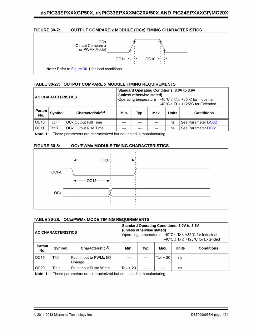
dsPIC33EPXXXGP50X, dsPIC33EPXXXMC20X/50X AND PIC24EPXXXGP/MC20X
FIGURE 30-7: OUTPUT COMPARE x MODULE (OCx) TIMING CHARACTERISTICS
FIGURE 30-8: OCx/PWMx MODULE TIMING CHARACTERISTICS
OCx
OC11 OC10
(Output Compare x
Note: Refer to Figure 30-1 for load conditions.
or PWMx Mode)
TABLE 30-27: OUTPUT COMPARE x MODULE TIMING REQUIREMENTS
AC CHARACTERISTICS
Standard Operating Conditions: 3.0V to 3.6V(unless otherwise stated)Operating temperature -40°C TA +85°C for Industrial
-40°C TA +125°C for Extended
Param No.
Symbol Characteristic(1) Min. Typ. Max. Units Conditions
OC10 TccF OCx Output Fall Time — — — ns See Parameter DO32
OC11 TccR OCx Output Rise Time — — — ns See Parameter DO31
Note 1: These parameters are characterized but not tested in manufacturing.
OCFA
OCx
OC20
OC15
TABLE 30-28: OCx/PWMx MODE TIMING REQUIREMENTS
AC CHARACTERISTICS
Standard Operating Conditions: 3.0V to 3.6V(unless otherwise stated)Operating temperature -40°C TA +85°C for Industrial
-40°C TA +125°C for Extended
Param No.
Symbol Characteristic(1) Min. Typ. Max. Units Conditions
OC15 TFD Fault Input to PWMx I/O Change
— — TCY + 20 ns
OC20 TFLT Fault Input Pulse Width TCY + 20 — — ns
Note 1: These parameters are characterized but not tested in manufacturing.
2011-2013 Microchip Technology Inc. DS70000657H-page 421

dsPIC33EPXXXGP50X, dsPIC33EPXXXMC20X/50X AND PIC24EPXXXGP/MC20X
FIGURE 30-9: HIGH-SPEED PWMx MODULE FAULT TIMING CHARACTERISTICS(dsPIC33EPXXXMC20X/50X and PIC24EPXXXMC20X DEVICES ONLY)
FIGURE 30-10: HIGH-SPEED PWMx MODULE TIMING CHARACTERISTICS(dsPIC33EPXXXMC20X/50X and PIC24EPXXXMC20X DEVICES ONLY)
TABLE 30-29: HIGH-SPEED PWMx MODULE TIMING REQUIREMENTS(dsPIC33EPXXXMC20X/50X and PIC24EPXXXMC20X DEVICES ONLY)
AC CHARACTERISTICS
Standard Operating Conditions: 3.0V to 3.6V(unless otherwise stated)Operating temperature -40°C TA +85°C for Industrial
-40°C TA +125°C for Extended
ParamNo.
Symbol Characteristic(1) Min. Typ. Max. Units Conditions
MP10 TFPWM PWMx Output Fall Time — — — ns See Parameter DO32
MP11 TRPWM PWMx Output Rise Time — — — ns See Parameter DO31
MP20 TFD Fault Input to PWMxI/O Change
— — 15 ns
MP30 TFH Fault Input Pulse Width 15 — — ns
Note 1: These parameters are characterized but not tested in manufacturing.
Fault Input
PWMx
MP30
MP20
(active-low)
PWMx
MP11 MP10
Note: Refer to Figure 30-1 for load conditions.
DS70000657H-page 422 2011-2013 Microchip Technology Inc.

dsPIC33EPXXXGP50X, dsPIC33EPXXXMC20X/50X AND PIC24EPXXXGP/MC20X
FIGURE 30-11: TIMERQ (QEI MODULE) EXTERNAL CLOCK TIMING CHARACTERISTICS (dsPIC33EPXXXMC20X/50X AND PIC24EPXXXMC20X DEVICES ONLY)
QEB
POSCNT
TQ10 TQ11
TQ15 TQ20
TABLE 30-30: QEI MODULE EXTERNAL CLOCK TIMING REQUIREMENTS (dsPIC33EPXXXMC20X/50X AND PIC24EPXXXMC20X DEVICES ONLY)
AC CHARACTERISTICS
Standard Operating Conditions: 3.0V to 3.6V(unless otherwise stated)Operating temperature -40°C TA +85°C for Industrial
-40°C TA +125°C for Extended
ParamNo.
Symbol Characteristic(1) Min. Typ. Max. Units Conditions
TQ10 TtQH TQCK High Time
Synchronous,with prescaler
Greater of 12.5 + 25or
(0.5 TCY/N) + 25
— — ns Must also meet Parameter TQ15
TQ11 TtQL TQCK Low Time
Synchronous,with prescaler
Greater of 12.5 + 25or
(0.5 TCY/N) + 25
— — ns Must also meet Parameter TQ15
TQ15 TtQP TQCP Input Period
Synchronous,with prescaler
Greater of 25 + 50or
(1 TCY/N) + 50
— — ns
TQ20 TCKEXTMRL Delay from External TQCK Clock Edge to Timer Increment
— 1 TCY —
Note 1: These parameters are characterized but not tested in manufacturing.
2011-2013 Microchip Technology Inc. DS70000657H-page 423

dsPIC33EPXXXGP50X, dsPIC33EPXXXMC20X/50X AND PIC24EPXXXGP/MC20X
FIGURE 30-12: QEA/QEB INPUT CHARACTERISTICS(dsPIC33EPXXXMC20X/50X and PIC24EPXXXMC20X DEVICES ONLY)
QEA(input)
QEB(input)
TQ35
TQ30
TQ41 TQ40
TQ35
QEBInternal
TQ36
TQ31
TQ31 TQ30
TABLE 30-31: QUADRATURE DECODER TIMING REQUIREMENTS(dsPIC33EPXXXMC20X/50X and PIC24EPXXXMC20X DEVICES ONLY)
AC CHARACTERISTICS
Standard Operating Conditions: 3.0V to 3.6V(unless otherwise stated)Operating temperature -40°C TA +85°C for Industrial
-40°C TA +125°C for Extended
ParamNo.
Symbol Characteristic(1) Typ.(2) Max. Units Conditions
TQ30 TQUL Quadrature Input Low Time 6 TCY — ns
TQ31 TQUH Quadrature Input High Time 6 TCY — ns
TQ35 TQUIN Quadrature Input Period 12 TCY — ns
TQ36 TQUP Quadrature Phase Period 3 TCY — ns
TQ40 TQUFL Filter Time to Recognize Low,with Digital Filter
3 * N * TCY — ns N = 1, 2, 4, 16, 32, 64, 128 and 256 (Note 3)
TQ41 TQUFH Filter Time to Recognize High,with Digital Filter
3 * N * TCY — ns N = 1, 2, 4, 16, 32, 64, 128 and 256 (Note 3)
Note 1: These parameters are characterized but not tested in manufacturing.
2: Data in “Typical” column is at 3.3V, +25°C unless otherwise stated. Parameters are for design guidance only and are not tested.
3: N = Index Channel Digital Filter Clock Divide Select bits. Refer to “Quadrature Encoder Interface (QEI)” (DS70601) in the “dsPIC33/PIC24 Family Reference Manual”. Please see the Microchip web site for the latest family reference manual sections.
DS70000657H-page 424 2011-2013 Microchip Technology Inc.

dsPIC33EPXXXGP50X, dsPIC33EPXXXMC20X/50X AND PIC24EPXXXGP/MC20X
FIGURE 30-13: QEI MODULE INDEX PULSE TIMING CHARACTERISTICS(dsPIC33EPXXXMC20X/50X and PIC24EPXXXMC20X DEVICES ONLY)
QEA(input)
QEB(input)
UngatedIndex
Index Internal
Position CounterReset
TQ51 TQ50
TQ55
TABLE 30-32: QEI INDEX PULSE TIMING REQUIREMENTS(dsPIC33EPXXXMC20X/50X and PIC24EPXXXMC20X DEVICES ONLY)
AC CHARACTERISTICS
Standard Operating Conditions: 3.0V to 3.6V(unless otherwise stated)Operating temperature -40°C TA +85°C for Industrial
-40°C TA +125°C for Extended
ParamNo.
Symbol Characteristic(1) Min. Max. Units Conditions
TQ50 TqiL Filter Time to Recognize Low,with Digital Filter
3 * N * TCY — ns N = 1, 2, 4, 16, 32, 64,128 and 256 (Note 2)
TQ51 TqiH Filter Time to Recognize High,with Digital Filter
3 * N * TCY — ns N = 1, 2, 4, 16, 32, 64,128 and 256 (Note 2)
TQ55 Tqidxr Index Pulse Recognized to PositionCounter Reset (ungated index)
3 TCY — ns
Note 1: These parameters are characterized but not tested in manufacturing.
2: Alignment of index pulses to QEA and QEB is shown for position counter Reset timing only. Shown for forward direction only (QEA leads QEB). Same timing applies for reverse direction (QEA lags QEB) but index pulse recognition occurs on the falling edge.
2011-2013 Microchip Technology Inc. DS70000657H-page 425

dsPIC33EPXXXGP50X, dsPIC33EPXXXMC20X/50X AND PIC24EPXXXGP/MC20X
TABLE 30-33: SPI2 MAXIMUM DATA/CLOCK RATE SUMMARY
FIGURE 30-14: SPI2 MASTER MODE (HALF-DUPLEX, TRANSMIT ONLY, CKE = 0) TIMING CHARACTERISTICS
AC CHARACTERISTICS
Standard Operating Conditions: 3.0V to 3.6V(unless otherwise stated)Operating temperature -40°C TA +85°C for Industrial
-40°C TA +125°C for Extended
Maximum Data Rate
Master Transmit Only (Half-Duplex)
Master Transmit/Receive
(Full-Duplex)
Slave Transmit/Receive
(Full-Duplex)CKE CKP SMP
15 MHz Table 30-33 — — 0,1 0,1 0,1
9 MHz — Table 30-34 — 1 0,1 1
9 MHz — Table 30-35 — 0 0,1 1
15 MHz — — Table 30-36 1 0 0
11 MHz — — Table 30-37 1 1 0
15 MHz — — Table 30-38 0 1 0
11 MHz — — Table 30-39 0 0 0
SCK2(CKP = 0)
SCK2(CKP = 1)
SDO2
SP10
SP21SP20SP35
SP20SP21
MSb LSbBit 14 - - - - - -1
SP30, SP31SP30, SP31
Note: Refer to Figure 30-1 for load conditions.
DS70000657H-page 426 2011-2013 Microchip Technology Inc.

dsPIC33EPXXXGP50X, dsPIC33EPXXXMC20X/50X AND PIC24EPXXXGP/MC20X
FIGURE 30-15: SPI2 MASTER MODE (HALF-DUPLEX, TRANSMIT ONLY, CKE = 1) TIMING CHARACTERISTICS
TABLE 30-34: SPI2 MASTER MODE (HALF-DUPLEX, TRANSMIT ONLY) TIMING REQUIREMENTS
AC CHARACTERISTICS
Standard Operating Conditions: 3.0V to 3.6V(unless otherwise stated)Operating temperature -40°C TA +85°C for Industrial
-40°C TA +125°C for Extended
Param. Symbol Characteristic(1) Min. Typ.(2) Max. Units Conditions
SP10 FscP Maximum SCK2 Frequency — — 15 MHz (Note 3)
SP20 TscF SCK2 Output Fall Time — — — ns See Parameter DO32 (Note 4)
SP21 TscR SCK2 Output Rise Time — — — ns See Parameter DO31 (Note 4)
SP30 TdoF SDO2 Data Output Fall Time — — — ns See Parameter DO32 (Note 4)
SP31 TdoR SDO2 Data Output Rise Time — — — ns See Parameter DO31 (Note 4)
SP35 TscH2doV,TscL2doV
SDO2 Data Output Valid after SCK2 Edge
— 6 20 ns
SP36 TdiV2scH,TdiV2scL
SDO2 Data Output Setup to First SCK2 Edge
30 — — ns
Note 1: These parameters are characterized, but are not tested in manufacturing.
2: Data in “Typical” column is at 3.3V, +25°C unless otherwise stated.
3: The minimum clock period for SCK2 is 66.7 ns. Therefore, the clock generated in Master mode must not violate this specification.
4: Assumes 50 pF load on all SPI2 pins.
SCK2(CKP = 0)
SCK2(CKP = 1)
SDO2
SP21SP20SP35
SP20SP21
MSb LSbBit 14 - - - - - -1
SP30, SP31
Note: Refer to Figure 30-1 for load conditions.
SP36
SP10
2011-2013 Microchip Technology Inc. DS70000657H-page 427

dsPIC33EPXXXGP50X, dsPIC33EPXXXMC20X/50X AND PIC24EPXXXGP/MC20X
FIGURE 30-16: SPI2 MASTER MODE (FULL-DUPLEX, CKE = 1, CKP = x, SMP = 1) TIMING CHARACTERISTICS
TABLE 30-35: SPI2 MASTER MODE (FULL-DUPLEX, CKE = 1, CKP = x, SMP = 1) TIMING REQUIREMENTS
AC CHARACTERISTICS
Standard Operating Conditions: 3.0V to 3.6V(unless otherwise stated)Operating temperature -40°C TA +85°C for Industrial
-40°C TA +125°C for Extended
Param. Symbol Characteristic(1) Min. Typ.(2) Max. Units Conditions
SP10 FscP Maximum SCK2 Frequency — — 9 MHz (Note 3)
SP20 TscF SCK2 Output Fall Time — — — ns See Parameter DO32 (Note 4)
SP21 TscR SCK2 Output Rise Time — — — ns See Parameter DO31 (Note 4)
SP30 TdoF SDO2 Data Output Fall Time — — — ns See Parameter DO32 (Note 4)
SP31 TdoR SDO2 Data Output Rise Time — — — ns See Parameter DO31 (Note 4)
SP35 TscH2doV,TscL2doV
SDO2 Data Output Valid afterSCK2 Edge
— 6 20 ns
SP36 TdoV2sc, TdoV2scL
SDO2 Data Output Setup toFirst SCK2 Edge
30 — — ns
SP40 TdiV2scH, TdiV2scL
Setup Time of SDI2 Data Input to SCK2 Edge
30 — — ns
SP41 TscH2diL, TscL2diL
Hold Time of SDI2 Data Inputto SCK2 Edge
30 — — ns
Note 1: These parameters are characterized, but are not tested in manufacturing.
2: Data in “Typical” column is at 3.3V, +25°C unless otherwise stated.
3: The minimum clock period for SCK2 is 111 ns. The clock generated in Master mode must not violate this specification.
4: Assumes 50 pF load on all SPI2 pins.
SCK2(CKP = 0)
SCK2(CKP = 1)
SDO2
SP21SP20SP35
SP20SP21
MSb LSbBit 14 - - - - - -1
SP30, SP31
Note: Refer to Figure 30-1 for load conditions.
SP36
SP41
LSb InBit 14 - - - -1SDI2
SP40
SP10
MSb In
DS70000657H-page 428 2011-2013 Microchip Technology Inc.

dsPIC33EPXXXGP50X, dsPIC33EPXXXMC20X/50X AND PIC24EPXXXGP/MC20X
FIGURE 30-17: SPI2 MASTER MODE (FULL-DUPLEX, CKE = 0, CKP = x, SMP = 1) TIMING CHARACTERISTICS
TABLE 30-36: SPI2 MASTER MODE (FULL-DUPLEX, CKE = 0, CKP = x, SMP = 1) TIMING REQUIREMENTS
AC CHARACTERISTICS
Standard Operating Conditions: 3.0V to 3.6V(unless otherwise stated)Operating temperature -40°C TA +85°C for Industrial
-40°C TA +125°C for Extended
Param. Symbol Characteristic(1) Min. Typ.(2) Max. Units Conditions
SP10 FscP Maximum SCK2 Frequency — — 9 MHz -40ºC to +125ºC (Note 3)
SP20 TscF SCK2 Output Fall Time — — — ns See Parameter DO32 (Note 4)
SP21 TscR SCK2 Output Rise Time — — — ns See Parameter DO31 (Note 4)
SP30 TdoF SDO2 Data Output Fall Time — — — ns See Parameter DO32 (Note 4)
SP31 TdoR SDO2 Data Output Rise Time — — — ns See Parameter DO31 (Note 4)
SP35 TscH2doV,TscL2doV
SDO2 Data Output Valid afterSCK2 Edge
— 6 20 ns
SP36 TdoV2scH, TdoV2scL
SDO2 Data Output Setup toFirst SCK2 Edge
30 — — ns
SP40 TdiV2scH, TdiV2scL
Setup Time of SDI2 Data Input to SCK2 Edge
30 — — ns
SP41 TscH2diL, TscL2diL
Hold Time of SDI2 Data Inputto SCK2 Edge
30 — — ns
Note 1: These parameters are characterized, but are not tested in manufacturing.
2: Data in “Typical” column is at 3.3V, +25°C unless otherwise stated.
3: The minimum clock period for SCK2 is 111 ns. The clock generated in Master mode must not violate this specification.
4: Assumes 50 pF load on all SPI2 pins.
SCK2(CKP = 0)
SCK2(CKP = 1)
SDO2
SDI2
SP40 SP41
SP21SP20SP35
SP20SP21
MSb LSbBit 14 - - - - - -1
LSb InBit 14 - - - -1
SP30, SP31SP30, SP31
Note: Refer to Figure 30-1 for load conditions.
SP36
SP10
MSb In
2011-2013 Microchip Technology Inc. DS70000657H-page 429

dsPIC33EPXXXGP50X, dsPIC33EPXXXMC20X/50X AND PIC24EPXXXGP/MC20X
FIGURE 30-18: SPI2 SLAVE MODE (FULL-DUPLEX, CKE = 1, CKP = 0, SMP = 0) TIMING CHARACTERISTICS
SS2
SCK2(CKP = 0)
SCK2(CKP = 1)
SDO2
SP60
SDI2
SP30, SP31
MSb Bit 14 - - - - - -1 LSb
SP51
Bit 14 - - - -1 LSb In
SP35
SP52
SP73SP72
SP72SP73
SP40
SP41
Note: Refer to Figure 30-1 for load conditions.
SP36
SP50
SP70
MSb In
DS70000657H-page 430 2011-2013 Microchip Technology Inc.

dsPIC33EPXXXGP50X, dsPIC33EPXXXMC20X/50X AND PIC24EPXXXGP/MC20X
TABLE 30-37: SPI2 SLAVE MODE (FULL-DUPLEX, CKE = 1, CKP = 0, SMP = 0) TIMING REQUIREMENTS
AC CHARACTERISTICS
Standard Operating Conditions: 3.0V to 3.6V(unless otherwise stated)Operating temperature -40°C TA +85°C for Industrial
-40°C TA +125°C for Extended
Param. Symbol Characteristic(1) Min. Typ.(2) Max. Units Conditions
SP70 FscP Maximum SCK2 Input Frequency
— — Lesser of FP or 15
MHz (Note 3)
SP72 TscF SCK2 Input Fall Time — — — ns See Parameter DO32 (Note 4)
SP73 TscR SCK2 Input Rise Time — — — ns See Parameter DO31 (Note 4)
SP30 TdoF SDO2 Data Output Fall Time — — — ns See Parameter DO32 (Note 4)
SP31 TdoR SDO2 Data Output Rise Time — — — ns See Parameter DO31 (Note 4)
SP35 TscH2doV,TscL2doV
SDO2 Data Output Valid afterSCK2 Edge
— 6 20 ns
SP36 TdoV2scH, TdoV2scL
SDO2 Data Output Setup toFirst SCK2 Edge
30 — — ns
SP40 TdiV2scH, TdiV2scL
Setup Time of SDI2 Data Inputto SCK2 Edge
30 — — ns
SP41 TscH2diL, TscL2diL
Hold Time of SDI2 Data Inputto SCK2 Edge
30 — — ns
SP50 TssL2scH, TssL2scL
SS2 to SCK2 or SCK2 Input
120 — — ns
SP51 TssH2doZ SS2 to SDO2 OutputHigh-Impedance
10 — 50 ns (Note 4)
SP52 TscH2ssHTscL2ssH
SS2 after SCK2 Edge 1.5 TCY + 40 — — ns (Note 4)
SP60 TssL2doV SDO2 Data Output Valid after SS2 Edge
— — 50 ns
Note 1: These parameters are characterized, but are not tested in manufacturing.
2: Data in “Typical” column is at 3.3V, +25°C unless otherwise stated.
3: The minimum clock period for SCK2 is 66.7 ns. Therefore, the SCK2 clock generated by the master must not violate this specification.
4: Assumes 50 pF load on all SPI2 pins.
2011-2013 Microchip Technology Inc. DS70000657H-page 431

dsPIC33EPXXXGP50X, dsPIC33EPXXXMC20X/50X AND PIC24EPXXXGP/MC20X
FIGURE 30-19: SPI2 SLAVE MODE (FULL-DUPLEX, CKE = 1, CKP = 1, SMP = 0) TIMING CHARACTERISTICS
SS2
SCK2(CKP = 0)
SCK2(CKP = 1)
SDO2
SP60
SDI2
SP30, SP31
MSb Bit 14 - - - - - -1 LSb
SP51
Bit 14 - - - -1 LSb In
SP35
SP52
SP73SP72
SP72SP73SP70
SP40
SP41
Note: Refer to Figure 30-1 for load conditions.
SP36
SP50
MSb In
DS70000657H-page 432 2011-2013 Microchip Technology Inc.
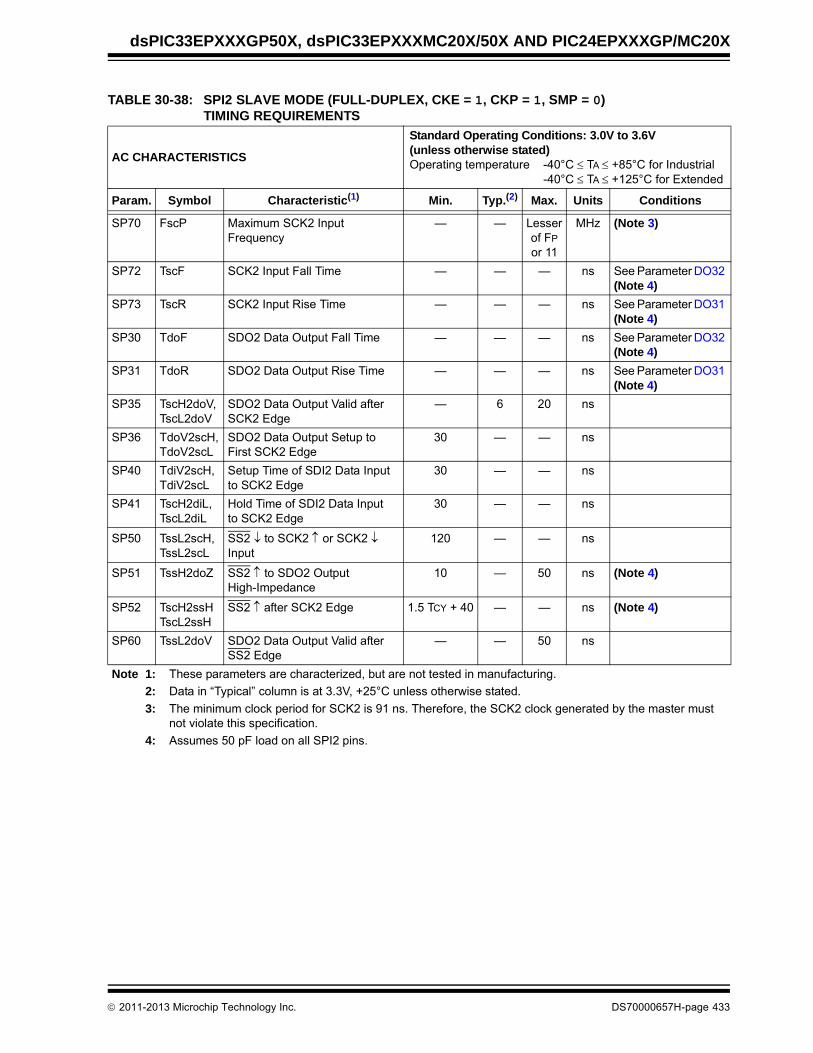
dsPIC33EPXXXGP50X, dsPIC33EPXXXMC20X/50X AND PIC24EPXXXGP/MC20X
TABLE 30-38: SPI2 SLAVE MODE (FULL-DUPLEX, CKE = 1, CKP = 1, SMP = 0) TIMING REQUIREMENTS
AC CHARACTERISTICS
Standard Operating Conditions: 3.0V to 3.6V(unless otherwise stated)Operating temperature -40°C TA +85°C for Industrial
-40°C TA +125°C for Extended
Param. Symbol Characteristic(1) Min. Typ.(2) Max. Units Conditions
SP70 FscP Maximum SCK2 Input Frequency
— — Lesser of FP or 11
MHz (Note 3)
SP72 TscF SCK2 Input Fall Time — — — ns See Parameter DO32 (Note 4)
SP73 TscR SCK2 Input Rise Time — — — ns See Parameter DO31 (Note 4)
SP30 TdoF SDO2 Data Output Fall Time — — — ns See Parameter DO32 (Note 4)
SP31 TdoR SDO2 Data Output Rise Time — — — ns See Parameter DO31 (Note 4)
SP35 TscH2doV,TscL2doV
SDO2 Data Output Valid afterSCK2 Edge
— 6 20 ns
SP36 TdoV2scH, TdoV2scL
SDO2 Data Output Setup toFirst SCK2 Edge
30 — — ns
SP40 TdiV2scH, TdiV2scL
Setup Time of SDI2 Data Inputto SCK2 Edge
30 — — ns
SP41 TscH2diL, TscL2diL
Hold Time of SDI2 Data Inputto SCK2 Edge
30 — — ns
SP50 TssL2scH, TssL2scL
SS2 to SCK2 or SCK2 Input
120 — — ns
SP51 TssH2doZ SS2 to SDO2 OutputHigh-Impedance
10 — 50 ns (Note 4)
SP52 TscH2ssHTscL2ssH
SS2 after SCK2 Edge 1.5 TCY + 40 — — ns (Note 4)
SP60 TssL2doV SDO2 Data Output Valid after SS2 Edge
— — 50 ns
Note 1: These parameters are characterized, but are not tested in manufacturing.
2: Data in “Typical” column is at 3.3V, +25°C unless otherwise stated.
3: The minimum clock period for SCK2 is 91 ns. Therefore, the SCK2 clock generated by the master must not violate this specification.
4: Assumes 50 pF load on all SPI2 pins.
2011-2013 Microchip Technology Inc. DS70000657H-page 433

dsPIC33EPXXXGP50X, dsPIC33EPXXXMC20X/50X AND PIC24EPXXXGP/MC20X
FIGURE 30-20: SPI2 SLAVE MODE (FULL-DUPLEX, CKE = 0, CKP = 1, SMP = 0) TIMING CHARACTERISTICS
SS2
SCK2(CKP = 0)
SCK2(CKP = 1)
SDO2
SP50
SP40
SP41
SP30, SP31 SP51
SP35
MSb LSbBit 14 - - - - - -1
Bit 14 - - - -1 LSb In
SP52
SP73SP72
SP72SP73
Note: Refer to Figure 30-1 for load conditions.
SDI2 MSb In
SP70
SP36
DS70000657H-page 434 2011-2013 Microchip Technology Inc.

dsPIC33EPXXXGP50X, dsPIC33EPXXXMC20X/50X AND PIC24EPXXXGP/MC20X
TABLE 30-39: SPI2 SLAVE MODE (FULL-DUPLEX, CKE = 0, CKP = 1, SMP = 0) TIMING REQUIREMENTS
AC CHARACTERISTICS
Standard Operating Conditions: 3.0V to 3.6V(unless otherwise stated)Operating temperature -40°C TA +85°C for Industrial
-40°C TA +125°C for Extended
Param. Symbol Characteristic(1) Min. Typ.(2) Max. Units Conditions
SP70 FscP Maximum SCK2 Input Frequency — — 15 MHz (Note 3)
SP72 TscF SCK2 Input Fall Time — — — ns See Parameter DO32 (Note 4)
SP73 TscR SCK2 Input Rise Time — — — ns See Parameter DO31 (Note 4)
SP30 TdoF SDO2 Data Output Fall Time — — — ns See Parameter DO32 (Note 4)
SP31 TdoR SDO2 Data Output Rise Time — — — ns See Parameter DO31 (Note 4)
SP35 TscH2doV,TscL2doV
SDO2 Data Output Valid afterSCK2 Edge
— 6 20 ns
SP36 TdoV2scH, TdoV2scL
SDO2 Data Output Setup toFirst SCK2 Edge
30 — — ns
SP40 TdiV2scH, TdiV2scL
Setup Time of SDI2 Data Inputto SCK2 Edge
30 — — ns
SP41 TscH2diL, TscL2diL
Hold Time of SDI2 Data Inputto SCK2 Edge
30 — — ns
SP50 TssL2scH, TssL2scL
SS2 to SCK2 or SCK2 Input
120 — — ns
SP51 TssH2doZ SS2 to SDO2 OutputHigh-Impedance
10 — 50 ns (Note 4)
SP52 TscH2ssHTscL2ssH
SS2 after SCK2 Edge 1.5 TCY + 40 — — ns (Note 4)
Note 1: These parameters are characterized, but are not tested in manufacturing.
2: Data in “Typical” column is at 3.3V, +25°C unless otherwise stated.
3: The minimum clock period for SCK2 is 66.7 ns. Therefore, the SCK2 clock generated by the master must not violate this specification.
4: Assumes 50 pF load on all SPI2 pins.
2011-2013 Microchip Technology Inc. DS70000657H-page 435
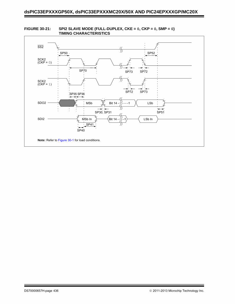
dsPIC33EPXXXGP50X, dsPIC33EPXXXMC20X/50X AND PIC24EPXXXGP/MC20X
FIGURE 30-21: SPI2 SLAVE MODE (FULL-DUPLEX, CKE = 0, CKP = 0, SMP = 0) TIMING CHARACTERISTICS
SS2
SCK2(CKP = 0)
SCK2(CKP = 1)
SDO2
SP50
SP40
SP41
SP30, SP31 SP51
SP35
MSb LSbBit 14 - - - - - -1
Bit 14 - - - -1 LSb In
SP52
SP73SP72
SP72SP73
Note: Refer to Figure 30-1 for load conditions.
SDI2
SP36
MSb In
SP70
DS70000657H-page 436 2011-2013 Microchip Technology Inc.

dsPIC33EPXXXGP50X, dsPIC33EPXXXMC20X/50X AND PIC24EPXXXGP/MC20X
TABLE 30-40: SPI2 SLAVE MODE (FULL-DUPLEX, CKE = 0, CKP = 0, SMP = 0) TIMING REQUIREMENTS
AC CHARACTERISTICS
Standard Operating Conditions: 3.0V to 3.6V(unless otherwise stated)Operating temperature -40°C TA +85°C for Industrial
-40°C TA +125°C for Extended
Param. Symbol Characteristic(1) Min. Typ.(2) Max. Units Conditions
SP70 FscP Maximum SCK2 Input Frequency — — 11 MHz (Note 3)
SP72 TscF SCK2 Input Fall Time — — — ns See Parameter DO32 (Note 4)
SP73 TscR SCK2 Input Rise Time — — — ns See Parameter DO31 (Note 4)
SP30 TdoF SDO2 Data Output Fall Time — — — ns See Parameter DO31 (Note 4)
SP31 TdoR SDO2 Data Output Rise Time — — — ns See Parameter DO31 (Note 4)
SP35 TscH2doV,TscL2doV
SDO2 Data Output Valid afterSCK2 Edge
— 6 20 ns
SP36 TdoV2scH, TdoV2scL
SDO2 Data Output Setup toFirst SCK2 Edge
30 — — ns
SP40 TdiV2scH, TdiV2scL
Setup Time of SDI2 Data Inputto SCK2 Edge
30 — — ns
SP41 TscH2diL, TscL2diL
Hold Time of SDI2 Data Inputto SCK2 Edge
30 — — ns
SP50 TssL2scH, TssL2scL
SS2 to SCK2 or SCK2 Input
120 — — ns
SP51 TssH2doZ SS2 to SDO2 OutputHigh-Impedance
10 — 50 ns (Note 4)
SP52 TscH2ssHTscL2ssH
SS2 after SCK2 Edge 1.5 TCY + 40 — — ns (Note 4)
Note 1: These parameters are characterized, but are not tested in manufacturing.
2: Data in “Typical” column is at 3.3V, +25°C unless otherwise stated.
3: The minimum clock period for SCK2 is 91 ns. Therefore, the SCK2 clock generated by the master must not violate this specification.
4: Assumes 50 pF load on all SPI2 pins.
2011-2013 Microchip Technology Inc. DS70000657H-page 437

dsPIC33EPXXXGP50X, dsPIC33EPXXXMC20X/50X AND PIC24EPXXXGP/MC20X
TABLE 30-41: SPI1 MAXIMUM DATA/CLOCK RATE SUMMARY
FIGURE 30-22: SPI1 MASTER MODE (HALF-DUPLEX, TRANSMIT ONLY, CKE = 0) TIMING CHARACTERISTICS
AC CHARACTERISTICS
Standard Operating Conditions: 3.0V to 3.6V(unless otherwise stated)Operating temperature -40°C TA +85°C for Industrial
-40°C TA +125°C for Extended
Maximum Data Rate
Master Transmit Only (Half-Duplex)
Master Transmit/Receive
(Full-Duplex)
Slave Transmit/Receive
(Full-Duplex)CKE CKP SMP
15 MHz Table 30-42 — — 0,1 0,1 0,1
10 MHz — Table 30-43 — 1 0,1 1
10 MHz — Table 30-44 — 0 0,1 1
15 MHz — — Table 30-45 1 0 0
11 MHz — — Table 30-46 1 1 0
15 MHz — — Table 30-47 0 1 0
11 MHz — — Table 30-48 0 0 0
SCK1(CKP = 0)
SCK1(CKP = 1)
SDO1
SP10
SP21SP20SP35
SP20SP21
MSb LSbBit 14 - - - - - -1
SP30, SP31SP30, SP31
Note: Refer to Figure 30-1 for load conditions.
DS70000657H-page 438 2011-2013 Microchip Technology Inc.

dsPIC33EPXXXGP50X, dsPIC33EPXXXMC20X/50X AND PIC24EPXXXGP/MC20X
FIGURE 30-23: SPI1 MASTER MODE (HALF-DUPLEX, TRANSMIT ONLY, CKE = 1) TIMING CHARACTERISTICS
TABLE 30-42: SPI1 MASTER MODE (HALF-DUPLEX, TRANSMIT ONLY) TIMING REQUIREMENTS
AC CHARACTERISTICS
Standard Operating Conditions: 3.0V to 3.6V(unless otherwise stated)Operating temperature -40°C TA +85°C for Industrial
-40°C TA +125°C for Extended
Param. Symbol Characteristic(1) Min. Typ.(2) Max. Units Conditions
SP10 FscP Maximum SCK1 Frequency — — 15 MHz (Note 3)
SP20 TscF SCK1 Output Fall Time — — — ns See Parameter DO32 (Note 4)
SP21 TscR SCK1 Output Rise Time — — — ns See Parameter DO31 (Note 4)
SP30 TdoF SDO1 Data Output Fall Time — — — ns See Parameter DO32 (Note 4)
SP31 TdoR SDO1 Data Output Rise Time — — — ns See Parameter DO31 (Note 4)
SP35 TscH2doV,TscL2doV
SDO1 Data Output Valid after SCK1 Edge
— 6 20 ns
SP36 TdiV2scH,TdiV2scL
SDO1 Data Output Setup to First SCK1 Edge
30 — — ns
Note 1: These parameters are characterized, but are not tested in manufacturing.
2: Data in “Typical” column is at 3.3V, +25°C unless otherwise stated.
3: The minimum clock period for SCK1 is 66.7 ns. Therefore, the clock generated in Master mode must not violate this specification.
4: Assumes 50 pF load on all SPI1 pins.
SCK1(CKP = 0)
SCK1(CKP = 1)
SDO1
SP21SP20SP35
SP20SP21
MSb LSbBit 14 - - - - - -1
SP30, SP31
Note: Refer to Figure 30-1 for load conditions.
SP36
SP10
2011-2013 Microchip Technology Inc. DS70000657H-page 439
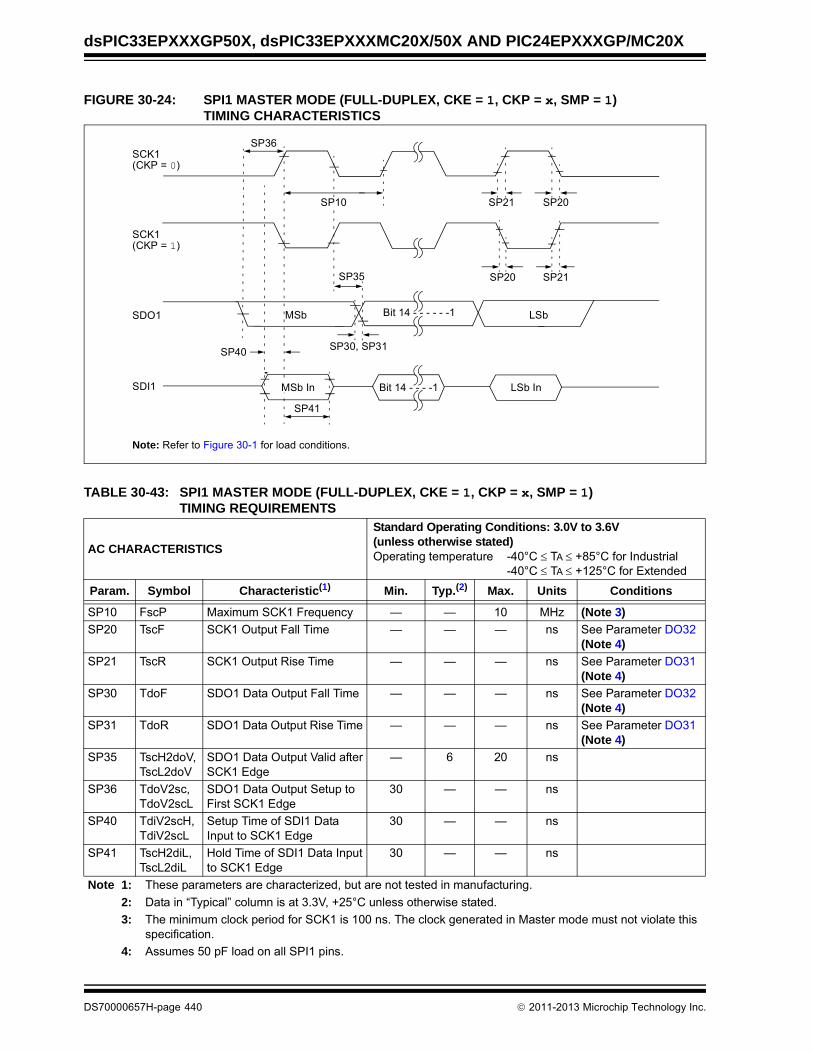
dsPIC33EPXXXGP50X, dsPIC33EPXXXMC20X/50X AND PIC24EPXXXGP/MC20X
FIGURE 30-24: SPI1 MASTER MODE (FULL-DUPLEX, CKE = 1, CKP = x, SMP = 1) TIMING CHARACTERISTICS
TABLE 30-43: SPI1 MASTER MODE (FULL-DUPLEX, CKE = 1, CKP = x, SMP = 1) TIMING REQUIREMENTS
AC CHARACTERISTICS
Standard Operating Conditions: 3.0V to 3.6V(unless otherwise stated)Operating temperature -40°C TA +85°C for Industrial
-40°C TA +125°C for Extended
Param. Symbol Characteristic(1) Min. Typ.(2) Max. Units Conditions
SP10 FscP Maximum SCK1 Frequency — — 10 MHz (Note 3)
SP20 TscF SCK1 Output Fall Time — — — ns See Parameter DO32 (Note 4)
SP21 TscR SCK1 Output Rise Time — — — ns See Parameter DO31 (Note 4)
SP30 TdoF SDO1 Data Output Fall Time — — — ns See Parameter DO32 (Note 4)
SP31 TdoR SDO1 Data Output Rise Time — — — ns See Parameter DO31 (Note 4)
SP35 TscH2doV,TscL2doV
SDO1 Data Output Valid afterSCK1 Edge
— 6 20 ns
SP36 TdoV2sc, TdoV2scL
SDO1 Data Output Setup toFirst SCK1 Edge
30 — — ns
SP40 TdiV2scH, TdiV2scL
Setup Time of SDI1 Data Input to SCK1 Edge
30 — — ns
SP41 TscH2diL, TscL2diL
Hold Time of SDI1 Data Inputto SCK1 Edge
30 — — ns
Note 1: These parameters are characterized, but are not tested in manufacturing.
2: Data in “Typical” column is at 3.3V, +25°C unless otherwise stated.
3: The minimum clock period for SCK1 is 100 ns. The clock generated in Master mode must not violate this specification.
4: Assumes 50 pF load on all SPI1 pins.
SCK1(CKP = 0)
SCK1(CKP = 1)
SDO1
SP21SP20SP35
SP20SP21
MSb LSbBit 14 - - - - - -1
SP30, SP31
Note: Refer to Figure 30-1 for load conditions.
SP36
SP41
LSb InBit 14 - - - -1SDI1
SP40
MSb In
SP10
DS70000657H-page 440 2011-2013 Microchip Technology Inc.

dsPIC33EPXXXGP50X, dsPIC33EPXXXMC20X/50X AND PIC24EPXXXGP/MC20X
FIGURE 30-25: SPI1 MASTER MODE (FULL-DUPLEX, CKE = 0, CKP = x, SMP = 1) TIMING CHARACTERISTICS
TABLE 30-44: SPI1 MASTER MODE (FULL-DUPLEX, CKE = 0, CKP = x, SMP = 1) TIMING REQUIREMENTS
AC CHARACTERISTICS
Standard Operating Conditions: 3.0V to 3.6V(unless otherwise stated)Operating temperature -40°C TA +85°C for Industrial
-40°C TA +125°C for Extended
Param. Symbol Characteristic(1) Min. Typ.(2) Max. Units Conditions
SP10 FscP Maximum SCK1 Frequency — — 10 MHz -40ºC to +125ºC(Note 3)
SP20 TscF SCK1 Output Fall Time — — — ns See Parameter DO32 (Note 4)
SP21 TscR SCK1 Output Rise Time — — — ns See Parameter DO31 (Note 4)
SP30 TdoF SDO1 Data Output Fall Time — — — ns See Parameter DO32 (Note 4)
SP31 TdoR SDO1 Data Output Rise Time — — — ns See Parameter DO31 (Note 4)
SP35 TscH2doV,TscL2doV
SDO1 Data Output Valid afterSCK1 Edge
— 6 20 ns
SP36 TdoV2scH, TdoV2scL
SDO1 Data Output Setup toFirst SCK1 Edge
30 — — ns
SP40 TdiV2scH, TdiV2scL
Setup Time of SDI1 Data Input to SCK1 Edge
30 — — ns
SP41 TscH2diL, TscL2diL
Hold Time of SDI1 Data Inputto SCK1 Edge
30 — — ns
Note 1: These parameters are characterized, but are not tested in manufacturing.
2: Data in “Typical” column is at 3.3V, +25°C unless otherwise stated.
3: The minimum clock period for SCK1 is 100 ns. The clock generated in Master mode must not violate this specification.
4: Assumes 50 pF load on all SPI1 pins.
SCK1(CKP = 0)
SCK1(CKP = 1)
SDO1
SDI1
SP40 SP41
SP21SP20SP35
SP20SP21
MSb LSbBit 14 - - - - - -1
LSb InBit 14 - - - -1
SP30, SP31SP30, SP31
Note: Refer to Figure 30-1 for load conditions.
SP36
MSb In
SP10
2011-2013 Microchip Technology Inc. DS70000657H-page 441
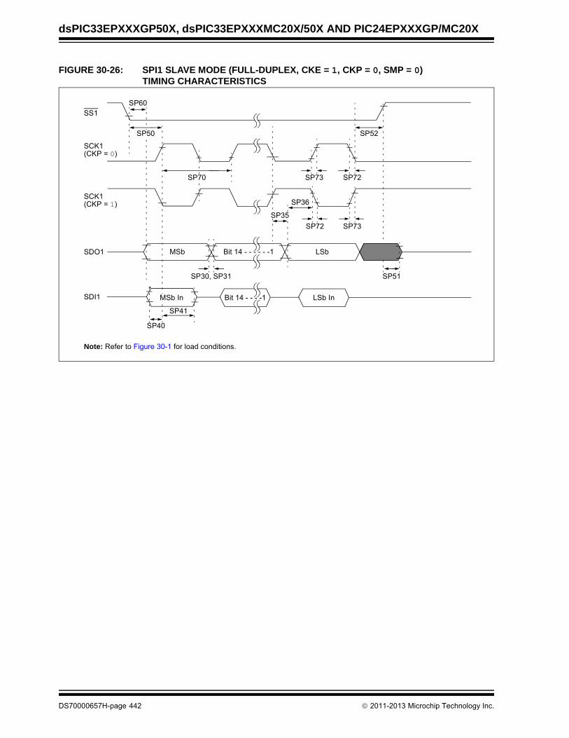
dsPIC33EPXXXGP50X, dsPIC33EPXXXMC20X/50X AND PIC24EPXXXGP/MC20X
FIGURE 30-26: SPI1 SLAVE MODE (FULL-DUPLEX, CKE = 1, CKP = 0, SMP = 0) TIMING CHARACTERISTICS
SS1
SCK1(CKP = 0)
SCK1(CKP = 1)
SDO1
SP60
SDI1
SP30, SP31
MSb Bit 14 - - - - - -1 LSb
SP51
Bit 14 - - - -1 LSb In
SP52
SP73SP72
SP72SP73
SP40
SP41
Note: Refer to Figure 30-1 for load conditions.
SP36
SP50
SP35
SP70
MSb In
DS70000657H-page 442 2011-2013 Microchip Technology Inc.
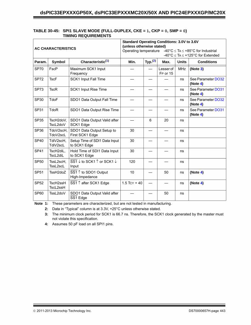
dsPIC33EPXXXGP50X, dsPIC33EPXXXMC20X/50X AND PIC24EPXXXGP/MC20X
TABLE 30-45: SPI1 SLAVE MODE (FULL-DUPLEX, CKE = 1, CKP = 0, SMP = 0) TIMING REQUIREMENTS
AC CHARACTERISTICS
Standard Operating Conditions: 3.0V to 3.6V(unless otherwise stated)Operating temperature -40°C TA +85°C for Industrial
-40°C TA +125°C for Extended
Param. Symbol Characteristic(1) Min. Typ.(2) Max. Units Conditions
SP70 FscP Maximum SCK1 Input Frequency
— — Lesser of FP or 15
MHz (Note 3)
SP72 TscF SCK1 Input Fall Time — — — ns See Parameter DO32 (Note 4)
SP73 TscR SCK1 Input Rise Time — — — ns See Parameter DO31 (Note 4)
SP30 TdoF SDO1 Data Output Fall Time — — — ns See Parameter DO32 (Note 4)
SP31 TdoR SDO1 Data Output Rise Time — — — ns See Parameter DO31 (Note 4)
SP35 TscH2doV,TscL2doV
SDO1 Data Output Valid afterSCK1 Edge
— 6 20 ns
SP36 TdoV2scH, TdoV2scL
SDO1 Data Output Setup toFirst SCK1 Edge
30 — — ns
SP40 TdiV2scH, TdiV2scL
Setup Time of SDI1 Data Inputto SCK1 Edge
30 — — ns
SP41 TscH2diL, TscL2diL
Hold Time of SDI1 Data Inputto SCK1 Edge
30 — — ns
SP50 TssL2scH, TssL2scL
SS1 to SCK1 or SCK1 Input
120 — — ns
SP51 TssH2doZ SS1 to SDO1 OutputHigh-Impedance
10 — 50 ns (Note 4)
SP52 TscH2ssHTscL2ssH
SS1 after SCK1 Edge 1.5 TCY + 40 — — ns (Note 4)
SP60 TssL2doV SDO1 Data Output Valid after SS1 Edge
— — 50 ns
Note 1: These parameters are characterized, but are not tested in manufacturing.
2: Data in “Typical” column is at 3.3V, +25°C unless otherwise stated.
3: The minimum clock period for SCK1 is 66.7 ns. Therefore, the SCK1 clock generated by the master must not violate this specification.
4: Assumes 50 pF load on all SPI1 pins.
2011-2013 Microchip Technology Inc. DS70000657H-page 443
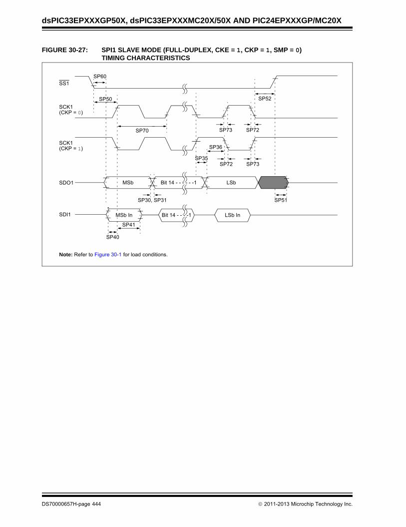
dsPIC33EPXXXGP50X, dsPIC33EPXXXMC20X/50X AND PIC24EPXXXGP/MC20X
FIGURE 30-27: SPI1 SLAVE MODE (FULL-DUPLEX, CKE = 1, CKP = 1, SMP = 0) TIMING CHARACTERISTICS
SS1
SCK1(CKP = 0)
SCK1(CKP = 1)
SDO1
SP60
SDI1
SP30, SP31
MSb Bit 14 - - - - - -1 LSb
SP51
Bit 14 - - - -1 LSb In
SP52
SP73SP72
SP72SP73SP70
SP40
SP41
Note: Refer to Figure 30-1 for load conditions.
SP36
SP50
SP35
MSb In
DS70000657H-page 444 2011-2013 Microchip Technology Inc.

dsPIC33EPXXXGP50X, dsPIC33EPXXXMC20X/50X AND PIC24EPXXXGP/MC20X
TABLE 30-46: SPI1 SLAVE MODE (FULL-DUPLEX, CKE = 1, CKP = 1, SMP = 0) TIMING REQUIREMENTS
AC CHARACTERISTICS
Standard Operating Conditions: 3.0V to 3.6V(unless otherwise stated)Operating temperature -40°C TA +85°C for Industrial
-40°C TA +125°C for Extended
Param. Symbol Characteristic(1) Min. Typ.(2) Max. Units Conditions
SP70 FscP Maximum SCK1 Input Frequency
— — Lesser of FP or 11
MHz (Note 3)
SP72 TscF SCK1 Input Fall Time — — — ns See Parameter DO32 (Note 4)
SP73 TscR SCK1 Input Rise Time — — — ns See Parameter DO31 (Note 4)
SP30 TdoF SDO1 Data Output Fall Time — — — ns See Parameter DO32 (Note 4)
SP31 TdoR SDO1 Data Output Rise Time — — — ns See Parameter DO31 (Note 4)
SP35 TscH2doV,TscL2doV
SDO1 Data Output Valid afterSCK1 Edge
— 6 20 ns
SP36 TdoV2scH, TdoV2scL
SDO1 Data Output Setup toFirst SCK1 Edge
30 — — ns
SP40 TdiV2scH, TdiV2scL
Setup Time of SDI1 Data Inputto SCK1 Edge
30 — — ns
SP41 TscH2diL, TscL2diL
Hold Time of SDI1 Data Inputto SCK1 Edge
30 — — ns
SP50 TssL2scH, TssL2scL
SS1 to SCK1 or SCK1 Input
120 — — ns
SP51 TssH2doZ SS1 to SDO1 OutputHigh-Impedance
10 — 50 ns (Note 4)
SP52 TscH2ssH,TscL2ssH
SS1 after SCK1 Edge 1.5 TCY + 40 — — ns (Note 4)
SP60 TssL2doV SDO1 Data Output Valid after SS1 Edge
— — 50 ns
Note 1: These parameters are characterized, but are not tested in manufacturing.
2: Data in “Typical” column is at 3.3V, +25°C unless otherwise stated.
3: The minimum clock period for SCK1 is 91 ns. Therefore, the SCK1 clock generated by the master must not violate this specification.
4: Assumes 50 pF load on all SPI1 pins.
2011-2013 Microchip Technology Inc. DS70000657H-page 445

dsPIC33EPXXXGP50X, dsPIC33EPXXXMC20X/50X AND PIC24EPXXXGP/MC20X
FIGURE 30-28: SPI1 SLAVE MODE (FULL-DUPLEX, CKE = 0, CKP = 1, SMP = 0) TIMING CHARACTERISTICS
SS1
SCK1(CKP = 0)
SCK1(CKP = 1)
SDO1
SP50
SP40
SP41
SP30, SP31 SP51
SP35
MSb LSbBit 14 - - - - - -1
Bit 14 - - - -1 LSb In
SP52
SP73SP72
SP72SP73
Note: Refer to Figure 30-1 for load conditions.
SDI1
SP70
SP36
MSb In
DS70000657H-page 446 2011-2013 Microchip Technology Inc.

dsPIC33EPXXXGP50X, dsPIC33EPXXXMC20X/50X AND PIC24EPXXXGP/MC20X
TABLE 30-47: SPI1 SLAVE MODE (FULL-DUPLEX, CKE = 0, CKP = 1, SMP = 0) TIMING REQUIREMENTS
AC CHARACTERISTICS
Standard Operating Conditions: 3.0V to 3.6V(unless otherwise stated)Operating temperature -40°C TA +85°C for Industrial
-40°C TA +125°C for Extended
Param. Symbol Characteristic(1) Min. Typ.(2) Max. Units Conditions
SP70 FscP Maximum SCK1 Input Frequency — — 15 MHz (Note 3)
SP72 TscF SCK1 Input Fall Time — — — ns See Parameter DO32 (Note 4)
SP73 TscR SCK1 Input Rise Time — — — ns See Parameter DO31 (Note 4)
SP30 TdoF SDO1 Data Output Fall Time — — — ns See Parameter DO32 (Note 4)
SP31 TdoR SDO1 Data Output Rise Time — — — ns See Parameter DO31 (Note 4)
SP35 TscH2doV,TscL2doV
SDO1 Data Output Valid afterSCK1 Edge
— 6 20 ns
SP36 TdoV2scH, TdoV2scL
SDO1 Data Output Setup toFirst SCK1 Edge
30 — — ns
SP40 TdiV2scH, TdiV2scL
Setup Time of SDI1 Data Inputto SCK1 Edge
30 — — ns
SP41 TscH2diL, TscL2diL
Hold Time of SDI1 Data Inputto SCK1 Edge
30 — — ns
SP50 TssL2scH, TssL2scL
SS1 to SCK1 or SCK1 Input
120 — — ns
SP51 TssH2doZ SS1 to SDO1 OutputHigh-Impedance
10 — 50 ns (Note 4)
SP52 TscH2ssH,TscL2ssH
SS1 after SCK1 Edge 1.5 TCY + 40 — — ns (Note 4)
Note 1: These parameters are characterized, but are not tested in manufacturing.
2: Data in “Typical” column is at 3.3V, +25°C unless otherwise stated.
3: The minimum clock period for SCK1 is 66.7 ns. Therefore, the SCK1 clock generated by the master must not violate this specification.
4: Assumes 50 pF load on all SPI1 pins.
2011-2013 Microchip Technology Inc. DS70000657H-page 447

dsPIC33EPXXXGP50X, dsPIC33EPXXXMC20X/50X AND PIC24EPXXXGP/MC20X
FIGURE 30-29: SPI1 SLAVE MODE (FULL-DUPLEX, CKE = 0, CKP = 0, SMP = 0) TIMING CHARACTERISTICS
SS1
SCK1(CKP = 0)
SCK1(CKP = 1)
SDO1
SP50
SP40
SP41
SP30, SP31 SP51
MSb LSbBit 14 - - - - - -1
Bit 14 - - - -1 LSb In
SP52
SP73SP72
SP72SP73
Note: Refer to Figure 30-1 for load conditions.
SDI1
SP70
SP35 SP36
MSb In
DS70000657H-page 448 2011-2013 Microchip Technology Inc.

dsPIC33EPXXXGP50X, dsPIC33EPXXXMC20X/50X AND PIC24EPXXXGP/MC20X
TABLE 30-48: SPI1 SLAVE MODE (FULL-DUPLEX, CKE = 0, CKP = 0, SMP = 0) TIMING REQUIREMENTS
AC CHARACTERISTICS
Standard Operating Conditions: 3.0V to 3.6V(unless otherwise stated)Operating temperature -40°C TA +85°C for Industrial
-40°C TA +125°C for Extended
Param. Symbol Characteristic(1) Min. Typ.(2) Max. Units Conditions
SP70 FscP Maximum SCK1 Input Frequency — — 11 MHz (Note 3)
SP72 TscF SCK1 Input Fall Time — — — ns See Parameter DO32 (Note 4)
SP73 TscR SCK1 Input Rise Time — — — ns See Parameter DO31 (Note 4)
SP30 TdoF SDO1 Data Output Fall Time — — — ns See Parameter DO32 (Note 4)
SP31 TdoR SDO1 Data Output Rise Time — — — ns See Parameter DO31 (Note 4)
SP35 TscH2doV,TscL2doV
SDO1 Data Output Valid afterSCK1 Edge
— 6 20 ns
SP36 TdoV2scH, TdoV2scL
SDO1 Data Output Setup toFirst SCK1 Edge
30 — — ns
SP40 TdiV2scH, TdiV2scL
Setup Time of SDI1 Data Inputto SCK1 Edge
30 — — ns
SP41 TscH2diL, TscL2diL
Hold Time of SDI1 Data Inputto SCK1 Edge
30 — — ns
SP50 TssL2scH, TssL2scL
SS1 to SCK1 or SCK1 Input
120 — — ns
SP51 TssH2doZ SS1 to SDO1 OutputHigh-Impedance
10 — 50 ns (Note 4)
SP52 TscH2ssH,TscL2ssH
SS1 after SCK1 Edge 1.5 TCY + 40 — — ns (Note 4)
Note 1: These parameters are characterized, but are not tested in manufacturing.
2: Data in “Typical” column is at 3.3V, +25°C unless otherwise stated.
3: The minimum clock period for SCK1 is 91 ns. Therefore, the SCK1 clock generated by the master must not violate this specification.
4: Assumes 50 pF load on all SPI1 pins.
2011-2013 Microchip Technology Inc. DS70000657H-page 449

dsPIC33EPXXXGP50X, dsPIC33EPXXXMC20X/50X AND PIC24EPXXXGP/MC20X
FIGURE 30-30: I2Cx BUS START/STOP BITS TIMING CHARACTERISTICS (MASTER MODE)
FIGURE 30-31: I2Cx BUS DATA TIMING CHARACTERISTICS (MASTER MODE)
SCLx
SDAx
StartCondition
StopCondition
Note: Refer to Figure 30-1 for load conditions.
IM30
IM31
IM33
IM34
IM11IM10 IM33
IM11
IM10
IM20
IM26
IM25
IM40 IM40 IM45
IM21
SCLx
SDAxIn
SDAxOut
Note: Refer to Figure 30-1 for load conditions.
DS70000657H-page 450 2011-2013 Microchip Technology Inc.
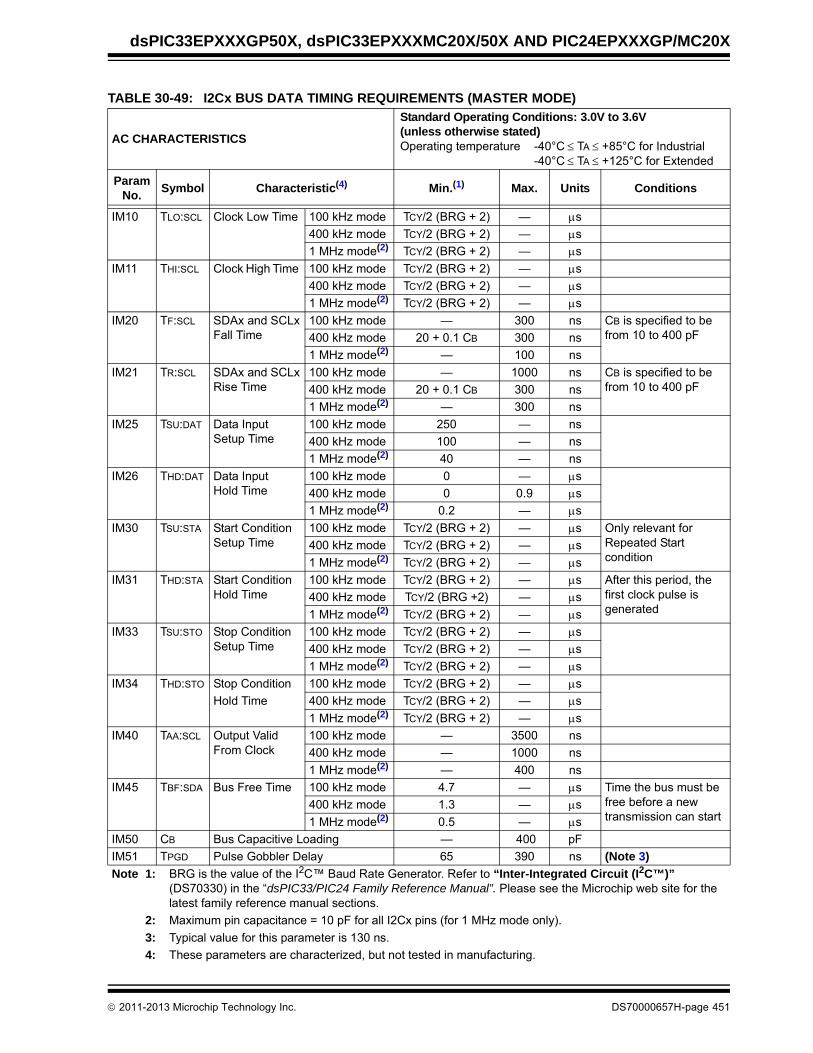
dsPIC33EPXXXGP50X, dsPIC33EPXXXMC20X/50X AND PIC24EPXXXGP/MC20X
TABLE 30-49: I2Cx BUS DATA TIMING REQUIREMENTS (MASTER MODE)
AC CHARACTERISTICS
Standard Operating Conditions: 3.0V to 3.6V(unless otherwise stated)Operating temperature -40°C TA +85°C for Industrial
-40°C TA +125°C for Extended
ParamNo.
Symbol Characteristic(4) Min.(1) Max. Units Conditions
IM10 TLO:SCL Clock Low Time 100 kHz mode TCY/2 (BRG + 2) — s
400 kHz mode TCY/2 (BRG + 2) — s
1 MHz mode(2) TCY/2 (BRG + 2) — s
IM11 THI:SCL Clock High Time 100 kHz mode TCY/2 (BRG + 2) — s
400 kHz mode TCY/2 (BRG + 2) — s
1 MHz mode(2) TCY/2 (BRG + 2) — s
IM20 TF:SCL SDAx and SCLxFall Time
100 kHz mode — 300 ns CB is specified to be from 10 to 400 pF400 kHz mode 20 + 0.1 CB 300 ns
1 MHz mode(2) — 100 ns
IM21 TR:SCL SDAx and SCLxRise Time
100 kHz mode — 1000 ns CB is specified to be from 10 to 400 pF400 kHz mode 20 + 0.1 CB 300 ns
1 MHz mode(2) — 300 ns
IM25 TSU:DAT Data InputSetup Time
100 kHz mode 250 — ns
400 kHz mode 100 — ns
1 MHz mode(2) 40 — ns
IM26 THD:DAT Data InputHold Time
100 kHz mode 0 — s
400 kHz mode 0 0.9 s
1 MHz mode(2) 0.2 — s
IM30 TSU:STA Start ConditionSetup Time
100 kHz mode TCY/2 (BRG + 2) — s Only relevant for Repeated Startcondition
400 kHz mode TCY/2 (BRG + 2) — s
1 MHz mode(2) TCY/2 (BRG + 2) — s
IM31 THD:STA Start Condition Hold Time
100 kHz mode TCY/2 (BRG + 2) — s After this period, thefirst clock pulse isgenerated
400 kHz mode TCY/2 (BRG +2) — s
1 MHz mode(2) TCY/2 (BRG + 2) — s
IM33 TSU:STO Stop Condition Setup Time
100 kHz mode TCY/2 (BRG + 2) — s
400 kHz mode TCY/2 (BRG + 2) — s
1 MHz mode(2) TCY/2 (BRG + 2) — s
IM34 THD:STO Stop Condition 100 kHz mode TCY/2 (BRG + 2) — s
Hold Time 400 kHz mode TCY/2 (BRG + 2) — s
1 MHz mode(2) TCY/2 (BRG + 2) — s
IM40 TAA:SCL Output Valid From Clock
100 kHz mode — 3500 ns
400 kHz mode — 1000 ns
1 MHz mode(2) — 400 ns
IM45 TBF:SDA Bus Free Time 100 kHz mode 4.7 — s Time the bus must be free before a newtransmission can start
400 kHz mode 1.3 — s
1 MHz mode(2) 0.5 — s
IM50 CB Bus Capacitive Loading — 400 pF
IM51 TPGD Pulse Gobbler Delay 65 390 ns (Note 3)
Note 1: BRG is the value of the I2C™ Baud Rate Generator. Refer to “Inter-Integrated Circuit (I2C™)” (DS70330) in the “dsPIC33/PIC24 Family Reference Manual”. Please see the Microchip web site for the latest family reference manual sections.
2: Maximum pin capacitance = 10 pF for all I2Cx pins (for 1 MHz mode only).
3: Typical value for this parameter is 130 ns.
4: These parameters are characterized, but not tested in manufacturing.
2011-2013 Microchip Technology Inc. DS70000657H-page 451
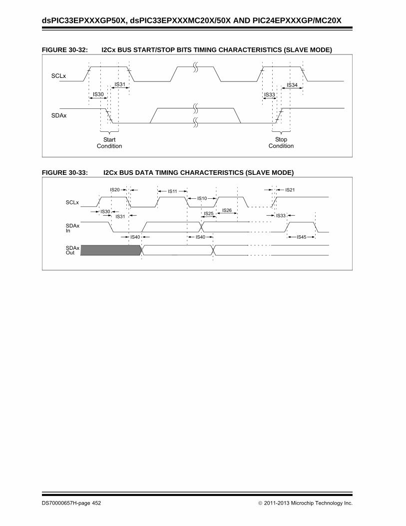
dsPIC33EPXXXGP50X, dsPIC33EPXXXMC20X/50X AND PIC24EPXXXGP/MC20X
FIGURE 30-32: I2Cx BUS START/STOP BITS TIMING CHARACTERISTICS (SLAVE MODE)
FIGURE 30-33: I2Cx BUS DATA TIMING CHARACTERISTICS (SLAVE MODE)
SCLx
SDAx
StartCondition
StopCondition
IS33
IS34
IS30
IS31
IS30IS31 IS33
IS11
IS10
IS20
IS25
IS40 IS40 IS45
IS21
SCLx
SDAxIn
SDAxOut
IS26
DS70000657H-page 452 2011-2013 Microchip Technology Inc.

dsPIC33EPXXXGP50X, dsPIC33EPXXXMC20X/50X AND PIC24EPXXXGP/MC20X
TABLE 30-50: I2Cx BUS DATA TIMING REQUIREMENTS (SLAVE MODE)
AC CHARACTERISTICS
Standard Operating Conditions: 3.0V to 3.6V(unless otherwise stated)Operating temperature -40°C TA +85°C for Industrial
-40°C TA +125°C for Extended
Param. No.
Symbol Characteristic(3) Min. Max. Units Conditions
IS10 TLO:SCL Clock Low Time 100 kHz mode 4.7 — s
400 kHz mode 1.3 — s
1 MHz mode(1) 0.5 — s
IS11 THI:SCL Clock High Time 100 kHz mode 4.0 — s Device must operate at a minimum of 1.5 MHz
400 kHz mode 0.6 — s Device must operate at a minimum of 10 MHz
1 MHz mode(1) 0.5 — s
IS20 TF:SCL SDAx and SCLxFall Time
100 kHz mode — 300 ns CB is specified to be from10 to 400 pF400 kHz mode 20 + 0.1 CB 300 ns
1 MHz mode(1) — 100 ns
IS21 TR:SCL SDAx and SCLxRise Time
100 kHz mode — 1000 ns CB is specified to be from10 to 400 pF400 kHz mode 20 + 0.1 CB 300 ns
1 MHz mode(1) — 300 ns
IS25 TSU:DAT Data InputSetup Time
100 kHz mode 250 — ns
400 kHz mode 100 — ns
1 MHz mode(1) 100 — ns
IS26 THD:DAT Data InputHold Time
100 kHz mode 0 — s
400 kHz mode 0 0.9 s
1 MHz mode(1) 0 0.3 s
IS30 TSU:STA Start ConditionSetup Time
100 kHz mode 4.7 — s Only relevant for Repeated Start condition400 kHz mode 0.6 — s
1 MHz mode(1) 0.25 — s
IS31 THD:STA Start Condition Hold Time
100 kHz mode 4.0 — s After this period, the first clock pulse is generated400 kHz mode 0.6 — s
1 MHz mode(1) 0.25 — s
IS33 TSU:STO Stop Condition Setup Time
100 kHz mode 4.7 — s
400 kHz mode 0.6 — s
1 MHz mode(1) 0.6 — s
IS34 THD:STO Stop ConditionHold Time
100 kHz mode 4 — s
400 kHz mode 0.6 — s
1 MHz mode(1) 0.25 s
IS40 TAA:SCL Output Valid From Clock
100 kHz mode 0 3500 ns
400 kHz mode 0 1000 ns
1 MHz mode(1) 0 350 ns
IS45 TBF:SDA Bus Free Time 100 kHz mode 4.7 — s Time the bus must be free before a new transmission can start
400 kHz mode 1.3 — s
1 MHz mode(1) 0.5 — s
IS50 CB Bus Capacitive Loading — 400 pF
IS51 TPGD Pulse Gobbler Delay 65 390 ns (Note 2)
Note 1: Maximum pin capacitance = 10 pF for all I2Cx pins (for 1 MHz mode only).
2: Typical value for this parameter is 130 ns.
3: These parameters are characterized, but not tested in manufacturing.
2011-2013 Microchip Technology Inc. DS70000657H-page 453
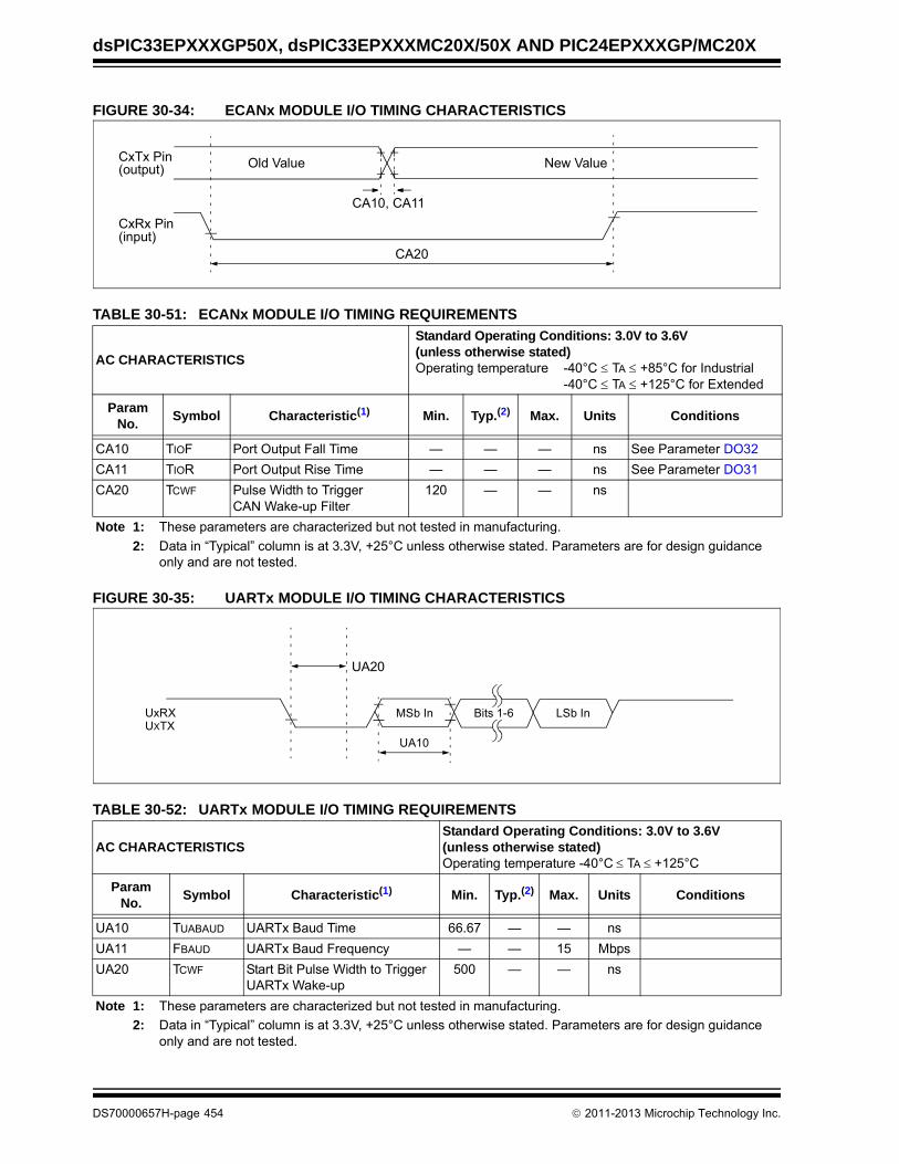
dsPIC33EPXXXGP50X, dsPIC33EPXXXMC20X/50X AND PIC24EPXXXGP/MC20X
FIGURE 30-34: ECANx MODULE I/O TIMING CHARACTERISTICS
TABLE 30-51: ECANx MODULE I/O TIMING REQUIREMENTS
FIGURE 30-35: UARTx MODULE I/O TIMING CHARACTERISTICS
TABLE 30-52: UARTx MODULE I/O TIMING REQUIREMENTS
AC CHARACTERISTICS
Standard Operating Conditions: 3.0V to 3.6V(unless otherwise stated)Operating temperature -40°C TA +85°C for Industrial
-40°C TA +125°C for Extended
ParamNo.
Symbol Characteristic(1) Min. Typ.(2) Max. Units Conditions
CA10 TIOF Port Output Fall Time — — — ns See Parameter DO32
CA11 TIOR Port Output Rise Time — — — ns See Parameter DO31
CA20 TCWF Pulse Width to TriggerCAN Wake-up Filter
120 — — ns
Note 1: These parameters are characterized but not tested in manufacturing.
2: Data in “Typical” column is at 3.3V, +25°C unless otherwise stated. Parameters are for design guidance only and are not tested.
AC CHARACTERISTICSStandard Operating Conditions: 3.0V to 3.6V(unless otherwise stated)Operating temperature -40°C TA +125°C
ParamNo.
Symbol Characteristic(1) Min. Typ.(2) Max. Units Conditions
UA10 TUABAUD UARTx Baud Time 66.67 — — ns
UA11 FBAUD UARTx Baud Frequency — — 15 Mbps
UA20 TCWF Start Bit Pulse Width to TriggerUARTx Wake-up
500 — — ns
Note 1: These parameters are characterized but not tested in manufacturing.
2: Data in “Typical” column is at 3.3V, +25°C unless otherwise stated. Parameters are for design guidance only and are not tested.
CxTx Pin(output)
CA10, CA11
Old Value New Value
CA20
CxRx Pin(input)
UA20
UxRX MSb In LSb InBits 1-6
UA10
UXTX
DS70000657H-page 454 2011-2013 Microchip Technology Inc.

dsPIC33EPXXXGP50X, dsPIC33EPXXXMC20X/50X AND PIC24EPXXXGP/MC20X
TABLE 30-53: OP AMP/COMPARATOR SPECIFICATIONS
DC CHARACTERISTICS
Standard Operating Conditions: 3.0V to 3.6V(unless otherwise stated)(1)
Operating temperature -40°C TA +85°C for Industrial-40°C TA +125°C for Extended
Param No.
Symbol Characteristic Min. Typ.(2) Max. Units Conditions
Comparator AC Characteristics
CM10 TRESP Response Time(3) — 19 — ns V+ input step of 100 mV,V- input held at VDD/2
CM11 TMC2OV Comparator Mode Change to Output Valid
— — 10 µs
Comparator DC Characteristics
CM30 VOFFSET Comparator Offset Voltage
— ±10 40 mV
CM31 VHYST Input Hysteresis Voltage(3)
— 30 — mV
CM32 TRISE/TFALL
Comparator Output Rise/Fall Time(3)
— 20 — ns 1 pF load capacitance on input
CM33 VGAIN Open-Loop Voltage Gain(3)
— 90 — db
CM34 VICM Input Common-Mode Voltage
AVSS — AVDD V
Op Amp AC Characteristics
CM20 SR Slew Rate(3) — 9 — V/µs 10 pF load
CM21a PM Phase Margin (Configuration A)(3,4)
— 55 — Degree G = 100V/V; 10 pF load
CM21b PM Phase Margin (Configuration B)(3,5)
— 40 — Degree G = 100V/V; 10 pF load
CM22 GM Gain Margin(3) — 20 — db G = 100V/V; 10 pF load
CM23a GBW Gain Bandwidth (Configuration A)(3,4)
— 10 — MHz 10 pF load
CM23b GBW Gain Bandwidth (Configuration B)(3,5)
— 6 — MHz 10 pF load
Note 1: Device is functional at VBORMIN < VDD < VDDMIN, but will have degraded performance. Device functionality is tested, but not characterized. Analog modules (ADC, op amp/comparator and comparator voltage reference) may have degraded performance. Refer to Parameter BO10 in Table 30-13 for the minimum and maximum BOR values.
2: Data in “Typ” column is at 3.3V, +25°C unless otherwise stated.
3: Parameter is characterized but not tested in manufacturing.
4: See Figure 25-6 for configuration information.
5: See Figure 25-7 for configuration information.
6: Resistances can vary by ±10% between op amps.
2011-2013 Microchip Technology Inc. DS70000657H-page 455

dsPIC33EPXXXGP50X, dsPIC33EPXXXMC20X/50X AND PIC24EPXXXGP/MC20X
Op Amp DC Characteristics
CM40 VCMR Common-Mode Input Voltage Range
AVSS — AVDD V
CM41 CMRR Common-Mode Rejection Ratio(3)
— 40 — db VCM = AVDD/2
CM42 VOFFSET Op Amp Offset Voltage(3)
— ±5 — mV
CM43 VGAIN Open-Loop Voltage Gain(3)
— 90 — db
CM44 IOS Input Offset Current — — — — See pad leakage currents in Table 30-11
CM45 IB Input Bias Current — — — — See pad leakage currents in Table 30-11
CM46 IOUT Output Current — — 420 µA With minimum value of RFEEDBACK (CM48)
CM48 RFEEDBACK Feedback Resistance Value
8 — — k
CM49a VOADC Output Voltage Measured at OAx Using ADC(3,4)
AVSS + 0.077AVSS + 0.037AVSS + 0.018
———
AVDD – 0.077AVDD – 0.037AVDD – 0.018
VVV
IOUT = 420 µAIOUT = 200 µAIOUT = 100 µA
CM49b VOUT Output Voltage Measured at OAxOUT Pin(3,4,5)
AVSS + 0.210AVSS + 0.100AVSS + 0.050
———
AVDD – 0.210AVDD – 0.100AVDD – 0.050
VVV
IOUT = 420 µAIOUT = 200 µAIOUT = 100 µA
CM51 RINT1(6) Internal Resistance 1 (Configuration A and B)(3,4,5)
198 264 317 Min = -40ºCTyp = +25ºCMax = +125ºC
TABLE 30-53: OP AMP/COMPARATOR SPECIFICATIONS (CONTINUED)
DC CHARACTERISTICS
Standard Operating Conditions: 3.0V to 3.6V(unless otherwise stated)(1)
Operating temperature -40°C TA +85°C for Industrial-40°C TA +125°C for Extended
Param No.
Symbol Characteristic Min. Typ.(2) Max. Units Conditions
Note 1: Device is functional at VBORMIN < VDD < VDDMIN, but will have degraded performance. Device functionality is tested, but not characterized. Analog modules (ADC, op amp/comparator and comparator voltage reference) may have degraded performance. Refer to Parameter BO10 in Table 30-13 for the minimum and maximum BOR values.
2: Data in “Typ” column is at 3.3V, +25°C unless otherwise stated.
3: Parameter is characterized but not tested in manufacturing.
4: See Figure 25-6 for configuration information.
5: See Figure 25-7 for configuration information.
6: Resistances can vary by ±10% between op amps.
DS70000657H-page 456 2011-2013 Microchip Technology Inc.
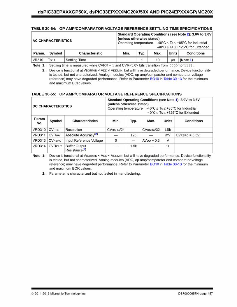
dsPIC33EPXXXGP50X, dsPIC33EPXXXMC20X/50X AND PIC24EPXXXGP/MC20X
TABLE 30-55: OP AMP/COMPARATOR VOLTAGE REFERENCE SPECIFICATIONS
TABLE 30-54: OP AMP/COMPARATOR VOLTAGE REFERENCE SETTLING TIME SPECIFICATIONS
AC CHARACTERISTICS
Standard Operating Conditions (see Note 2): 3.0V to 3.6V(unless otherwise stated)Operating temperature -40°C TA +85°C for Industrial
-40°C TA +125°C for Extended
Param. Symbol Characteristic Min. Typ. Max. Units Conditions
VR310 TSET Settling Time — 1 10 s (Note 1)
Note 1: Settling time is measured while CVRR = 1 and CVR<3:0> bits transition from ‘0000’ to ‘1111’.
2: Device is functional at VBORMIN < VDD < VDDMIN, but will have degraded performance. Device functionality is tested, but not characterized. Analog modules (ADC, op amp/comparator and comparator voltage reference) may have degraded performance. Refer to Parameter BO10 in Table 30-13 for the minimum and maximum BOR values.
DC CHARACTERISTICS
Standard Operating Conditions (see Note 1): 3.0V to 3.6V(unless otherwise stated)Operating temperature -40°C TA +85°C for Industrial
-40°C TA +125°C for Extended
ParamNo.
Symbol Characteristics Min. Typ. Max. Units Conditions
VRD310 CVRES Resolution CVRSRC/24 — CVRSRC/32 LSb
VRD311 CVRAA Absolute Accuracy(2) — ±25 — mV CVRSRC = 3.3V
VRD313 CVRSRC Input Reference Voltage 0 — AVDD + 0.3 V
VRD314 CVROUT Buffer Output Resistance(2)
— 1.5k —
Note 1: Device is functional at VBORMIN < VDD < VDDMIN, but will have degraded performance. Device functionality is tested, but not characterized. Analog modules (ADC, op amp/comparator and comparator voltage reference) may have degraded performance. Refer to Parameter BO10 in Table 30-13 for the minimum and maximum BOR values.
2: Parameter is characterized but not tested in manufacturing.
2011-2013 Microchip Technology Inc. DS70000657H-page 457

dsPIC33EPXXXGP50X, dsPIC33EPXXXMC20X/50X AND PIC24EPXXXGP/MC20X
TABLE 30-56: CTMU CURRENT SOURCE SPECIFICATIONS
DC CHARACTERISTICS
Standard Operating Conditions:3.0V to 3.6V(unless otherwise stated)Operating temperature -40°C TA +85°C for Industrial
-40°C TA +125°C for Extended
Param No.
Symbol Characteristic Min. Typ. Max. Units Conditions
CTMU Current Source
CTMUI1 IOUT1 Base Range(1) 0.29 — 0.77 µA CTMUICON<9:8> = 01
CTMUI2 IOUT2 10x Range(1) 3.85 — 7.7 µA CTMUICON<9:8> = 10
CTMUI3 IOUT3 100x Range(1) 38.5 — 77 µA CTMUICON<9:8> = 11
CTMUI4 IOUT4 1000x Range(1) 385 — 770 µA CTMUICON<9:8> = 00
CTMUFV1 VF Temperature Diode ForwardVoltage(1,2)
— 0.598 — V TA = +25°C, CTMUICON<9:8> = 01
— 0.658 — V TA = +25°C, CTMUICON<9:8> = 10
— 0.721 — V TA = +25°C, CTMUICON<9:8> = 11
CTMUFV2 VFVR Temperature Diode Rate ofChange(1,2,3)
— -1.92 — mV/ºC CTMUICON<9:8> = 01
— -1.74 — mV/ºC CTMUICON<9:8> = 10
— -1.56 — mV/ºC CTMUICON<9:8> = 11
Note 1: Nominal value at center point of current trim range (CTMUICON<15:10> = 000000).
2: Parameters are characterized but not tested in manufacturing.
3: Measurements taken with the following conditions:
• VREF+ = AVDD = 3.3V• ADC configured for 10-bit mode• ADC module configured for conversion speed of 500 ksps• All PMDx bits are cleared (PMDx = 0)• Executing a while(1) statement• Device operating from the FRC with no PLL
DS70000657H-page 458 2011-2013 Microchip Technology Inc.

dsPIC33EPXXXGP50X, dsPIC33EPXXXMC20X/50X AND PIC24EPXXXGP/MC20X
TABLE 30-57: ADC MODULE SPECIFICATIONS
AC CHARACTERISTICS
Standard Operating Conditions: 3.0V to 3.6V(unless otherwise stated)(1)
Operating temperature -40°C TA +85°C for Industrial-40°C TA +125°C for Extended
Param No.
Symbol Characteristic Min. Typ. Max. Units Conditions
Device Supply
AD01 AVDD Module VDD Supply Greater of:VDD – 0.3
or 3.0
— Lesser of:VDD + 0.3
or 3.6
V
AD02 AVSS Module VSS Supply VSS – 0.3 — VSS + 0.3 V
Reference Inputs
AD05 VREFH Reference Voltage High AVSS + 2.5 — AVDD V VREFH = VREF+VREFL = VREF- (Note 1)
AD05a 3.0 — 3.6 V VREFH = AVDD
VREFL = AVSS = 0
AD06 VREFL Reference Voltage Low AVSS — AVDD – 2.5 V (Note 1)
AD06a 0 — 0 V VREFH = AVDD
VREFL = AVSS = 0
AD07 VREF Absolute Reference Voltage
2.5 — 3.6 V VREF = VREFH - VREFL
AD08 IREF Current Drain ——
——
10600
AA
ADC offADC on
AD09 IAD Operating Current(2) — 5 — mA ADC operating in 10-bit mode (Note 1)
— 2 — mA ADC operating in 12-bit mode (Note 1)
Analog Input
AD12 VINH Input Voltage Range VINH
VINL — VREFH V This voltage reflects Sample-and-Hold Channels 0, 1, 2 and 3 (CH0-CH3), positive input
AD13 VINL Input Voltage Range VINL
VREFL — AVSS + 1V V This voltage reflects Sample-and-Hold Channels 0, 1, 2 and 3 (CH0-CH3), negative input
AD17 RIN Recommended Impedance of Analog Voltage Source
— — 200 Impedance to achieve maximum performance of ADC
Note 1: Device is functional at VBORMIN < VDD < VDDMIN, but will have degraded performance. Device functionality is tested, but not characterized. Analog modules (ADC, op amp/comparator and comparator voltage reference) may have degraded performance. Refer to Parameter BO10 in Table 30-13 for the minimum and maximum BOR values.
2: Parameter is characterized but not tested in manufacturing.
2011-2013 Microchip Technology Inc. DS70000657H-page 459

dsPIC33EPXXXGP50X, dsPIC33EPXXXMC20X/50X AND PIC24EPXXXGP/MC20X
TABLE 30-58: ADC MODULE SPECIFICATIONS (12-BIT MODE)
AC CHARACTERISTICS
Standard Operating Conditions: 3.0V to 3.6V(unless otherwise stated)(1)
Operating temperature -40°C TA +85°C for Industrial-40°C TA +125°C for Extended
Param No.
Symbol Characteristic Min. Typ. Max. Units Conditions
ADC Accuracy (12-Bit Mode)
AD20a Nr Resolution 12 Data Bits bits
AD21a INL Integral Nonlinearity -2.5 — 2.5 LSb -40°C TA +85°C (Note 2)
-5.5 — 5.5 LSb +85°C TA +125°C (Note 2)
AD22a DNL Differential Nonlinearity -1 — 1 LSb -40°C TA +85°C (Note 2)
-1 — 1 LSb +85°C TA +125°C (Note 2)
AD23a GERR Gain Error(3) -10 — 10 LSb -40°C TA +85°C (Note 2)
-10 — 10 LSb +85°C TA +125°C (Note 2)
AD24a EOFF Offset Error -5 — 5 LSb -40°C TA +85°C (Note 2)
-5 — 5 LSb +85°C TA +125°C (Note 2)
AD25a — Monotonicity — — — — Guaranteed
Dynamic Performance (12-Bit Mode)
AD30a THD Total Harmonic Distortion(3) — 75 — dB
AD31a SINAD Signal to Noise andDistortion(3)
— 68 — dB
AD32a SFDR Spurious Free DynamicRange(3)
— 80 — dB
AD33a FNYQ Input Signal Bandwidth(3) — 250 — kHz
AD34a ENOB Effective Number of Bits(3) 11.09 11.3 — bits
Note 1: Device is functional at VBORMIN < VDD < VDDMIN, but will have degraded performance. Device functionality is tested, but not characterized. Analog modules (ADC, op amp/comparator and comparator voltage reference) may have degraded performance. Refer to Parameter BO10 in Table 30-13 for the minimum and maximum BOR values.
2: For all accuracy specifications, VINL = AVSS = VREFL = 0V and AVDD = VREFH = 3.6V.
3: Parameters are characterized but not tested in manufacturing.
DS70000657H-page 460 2011-2013 Microchip Technology Inc.

dsPIC33EPXXXGP50X, dsPIC33EPXXXMC20X/50X AND PIC24EPXXXGP/MC20X
TABLE 30-59: ADC MODULE SPECIFICATIONS (10-BIT MODE)
AC CHARACTERISTICS
Standard Operating Conditions: 3.0V to 3.6V(unless otherwise stated)(1)
Operating temperature -40°C TA +85°C for Industrial-40°C TA +125°C for Extended
Param No.
Symbol Characteristic Min. Typ. Max. Units Conditions
ADC Accuracy (10-Bit Mode)
AD20b Nr Resolution 10 Data Bits bits
AD21b INL Integral Nonlinearity -0.625 — 0.625 LSb -40°C TA +85°C (Note 2)
-1.5 — 1.5 LSb +85°C TA +125°C (Note 2)
AD22b DNL Differential Nonlinearity -0.25 — 0.25 LSb -40°C TA +85°C (Note 2)
-0.25 — 0.25 LSb +85°C TA +125°C (Note 2)
AD23b GERR Gain Error -2.5 — 2.5 LSb -40°C TA +85°C (Note 2)
-2.5 — 2.5 LSb +85°C TA +125°C (Note 2)
AD24b EOFF Offset Error -1.25 — 1.25 LSb -40°C TA +85°C (Note 2)
-1.25 — 1.25 LSb +85°C TA +125°C (Note 2)
AD25b — Monotonicity — — — — Guaranteed
Dynamic Performance (10-Bit Mode)
AD30b THD Total Harmonic Distortion(3) — 64 — dB
AD31b SINAD Signal to Noise andDistortion(3)
— 57 — dB
AD32b SFDR Spurious Free DynamicRange(3)
— 72 — dB
AD33b FNYQ Input Signal Bandwidth(3) — 550 — kHz
AD34b ENOB Effective Number of Bits(3) — 9.4 — bits
Note 1: Device is functional at VBORMIN < VDD < VDDMIN, but will have degraded performance. Device functionality is tested, but not characterized. Analog modules (ADC, op amp/comparator and comparator voltage reference) may have degraded performance. Refer to Parameter BO10 in Table 30-13 for the minimum and maximum BOR values.
2: For all accuracy specifications, VINL = AVSS = VREFL = 0V and AVDD = VREFH = 3.6V.
3: Parameters are characterized but not tested in manufacturing.
2011-2013 Microchip Technology Inc. DS70000657H-page 461

dsPIC33EPXXXGP50X, dsPIC33EPXXXMC20X/50X AND PIC24EPXXXGP/MC20X
FIGURE 30-36: ADC CONVERSION (12-BIT MODE) TIMING CHARACTERISTICS (ASAM = 0, SSRC<2:0> = 000, SSRCG = 0)
AD55TSAMP
Set SAMP
AD61
ADCLK
Instruction
SAMP
AD60
DONE
AD1IF
1 2 3 4 5 6 87
1 – Software sets AD1CON1. SAMP to start sampling.
2 – Sampling starts after discharge period. TSAMP is described in
3 – Software clears AD1CON1. SAMP to start conversion.
4 – Sampling ends, conversion sequence starts.
5 – Convert bit 11.
9 – One TAD for end of conversion.
AD50
9
6 – Convert bit 10.
7 – Convert bit 1.
8 – Convert bit 0.
Execution
“dsPIC33/PIC24 Family Reference Manual”. “Analog-to-Digital Converter (ADC)” (DS70621) in the
Clear SAMP
DS70000657H-page 462 2011-2013 Microchip Technology Inc.

dsPIC33EPXXXGP50X, dsPIC33EPXXXMC20X/50X AND PIC24EPXXXGP/MC20X
TABLE 30-60: ADC CONVERSION (12-BIT MODE) TIMING REQUIREMENTS
AC CHARACTERISTICS
Standard Operating Conditions: 3.0V to 3.6V(unless otherwise stated)(1)
Operating temperature -40°C TA +85°C for Industrial-40°C TA +125°C for Extended
Param No.
Symbol Characteristic Min. Typ. Max. Units Conditions
Clock Parameters
AD50 TAD ADC Clock Period 117.6 — — ns
AD51 tRC ADC Internal RC Oscillator Period(2) — 250 — ns
Conversion Rate
AD55 tCONV Conversion Time — 14 TAD ns
AD56 FCNV Throughput Rate — — 500 ksps
AD57a TSAMP Sample Time when Sampling any ANx Input
3 TAD — — —
AD57b TSAMP Sample Time when Sampling the Op Amp Outputs (Configuration A and Configuration B)(4,5)
3 TAD — — —
Timing Parameters
AD60 tPCS Conversion Start from Sample Trigger(2,3)
2 TAD — 3 TAD — Auto-convert trigger is not selected
AD61 tPSS Sample Start from SettingSample (SAMP) bit(2,3)
2 TAD — 3 TAD —
AD62 tCSS Conversion Completion toSample Start (ASAM = 1)(2,3)
— 0.5 TAD — —
AD63 tDPU Time to Stabilize Analog Stagefrom ADC Off to ADC On(2,3)
— — 20 s (Note 6)
Note 1: Device is functional at VBORMIN < VDD < VDDMIN, but will have degraded performance. Device functionality is tested, but not characterized. Analog modules (ADC, op amp/comparator and comparator voltage reference) may have degraded performance. Refer to Parameter BO10 in Table 30-13 for the minimum and maximum BOR values.
2: Parameters are characterized but not tested in manufacturing.
3: Because the sample caps will eventually lose charge, clock rates below 10 kHz may affect linearity performance, especially at elevated temperatures.
4: See Figure 25-6 for configuration information.
5: See Figure 25-7 for configuration information.
6: The parameter, tDPU, is the time required for the ADC module to stabilize at the appropriate level when the module is turned on (ADON (AD1CON1<15>) = 1). During this time, the ADC result is indeterminate.
2011-2013 Microchip Technology Inc. DS70000657H-page 463

dsPIC33EPXXXGP50X, dsPIC33EPXXXMC20X/50X AND PIC24EPXXXGP/MC20X
FIGURE 30-37: ADC CONVERSION (10-BIT MODE) TIMING CHARACTERISTICS(CHPS<1:0> = 01, SIMSAM = 0, ASAM = 0, SSRC<2:0> = 000, SSRCG = 0)
FIGURE 30-38: ADC CONVERSION (10-BIT MODE) TIMING CHARACTERISTICS (CHPS<1:0> = 01, SIMSAM = 0, ASAM = 1, SSRC<2:0> = 111, SSRCG = 0, SAMC<4:0> = 00010)
TSAMP
Set SAMP
AD61
ADCLK
Instruction
SAMP
AD60
DONE
AD1IF
1 2 3 4 5 6 8 5 6 7
1 – Software sets AD1CON1. SAMP to start sampling.
2 – Sampling starts after discharge period. TSAMP is described in
3 – Software clears AD1CON1. SAMP to start conversion.
4 – Sampling ends, conversion sequence starts.
5 – Convert bit 9.
8 – One TAD for end of conversion.
AD50
7 8
6 – Convert bit 8.
7 – Convert bit 0.
Execution
“dsPIC33/PIC24 Family Reference Manual”.“Analog-to-Digital Converter (ADC)” (DS70621) in the
Clear SAMP
AD55 AD55
1 2 3 4 5 6 4 5 6 8
1 – Software sets AD1CON1. ADON to start AD operation.
2 – Sampling starts after discharge period. TSAMP is described in
3 – Convert bit 9.
4 – Convert bit 8.
5 – Convert bit 0.
7 3
6 – One TAD for end of conversion.
7 – Begin conversion of next channel.
8 – Sample for time specified by SAMC<4:0>.
ADCLK
Instruction Set ADONExecution
SAMP
TSAMP
AD1IF
DONE
AD55 AD55 TSAMP AD55
AD50
“Analog-to-Digital Converter (ADC)” (DS70621) in the “dsPIC33/PIC24 Family Reference Manual”.
AD62
DS70000657H-page 464 2011-2013 Microchip Technology Inc.

dsPIC33EPXXXGP50X, dsPIC33EPXXXMC20X/50X AND PIC24EPXXXGP/MC20X
TABLE 30-61: ADC CONVERSION (10-BIT MODE) TIMING REQUIREMENTS
AC CHARACTERISTICS
Standard Operating Conditions: 3.0V to 3.6V(unless otherwise stated)(1)
Operating temperature -40°C TA +85°C for Industrial-40°C TA +125°C for Extended
Param No.
Symbol Characteristic Min. Typ. Max. Units Conditions
Clock Parameters
AD50 TAD ADC Clock Period 76 — — ns
AD51 tRC ADC Internal RC Oscillator Period(2) — 250 — ns
Conversion Rate
AD55 tCONV Conversion Time — 12 TAD — —
AD56 FCNV Throughput Rate — — 1.1 Msps Using simultaneous sampling
AD57a TSAMP Sample Time when Sampling any ANx Input
2 TAD — — —
AD57b TSAMP Sample Time when Sampling the Op Amp Outputs (Configuration A and Configuration B)(4,5)
4 TAD — — —
Timing Parameters
AD60 tPCS Conversion Start from SampleTrigger(2,3)
2 TAD — 3 TAD — Auto-convert trigger is not selected
AD61 tPSS Sample Start from SettingSample (SAMP) bit(2,3))
2 TAD — 3 TAD —
AD62 tCSS Conversion Completion toSample Start (ASAM = 1)(2,3)
— 0.5 TAD — —
AD63 tDPU Time to Stabilize Analog Stage from ADC Off to ADC On(2,3)
— — 20 s (Note 6)
Note 1: Device is functional at VBORMIN < VDD < VDDMIN, but will have degraded performance. Device functionality is tested, but not characterized. Analog modules (ADC, op amp/comparator and comparator voltage reference) may have degraded performance. Refer to Parameter BO10 in Table 30-13 for the minimum and maximum BOR values.
2: Parameters are characterized but not tested in manufacturing.
3: Because the sample caps will eventually lose charge, clock rates below 10 kHz may affect linearity performance, especially at elevated temperatures.
4: See Figure 25-6 for configuration information.
5: See Figure 25-7 for configuration information.
6: The parameter, tDPU, is the time required for the ADC module to stabilize at the appropriate level when the module is turned on (ADON (AD1CON1<15>) = 1). During this time, the ADC result is indeterminate.
TABLE 30-62: DMA MODULE TIMING REQUIREMENTS
AC CHARACTERISTICS
Standard Operating Conditions: 3.0V to 3.6V(unless otherwise stated)Operating temperature -40°C TA +85°C for Industrial
-40°C TA +125°C for Extended
Param No.
Characteristic Min. Typ.(1) Max. Units Conditions
DM1 DMA Byte/Word Transfer Latency 1 TCY(2) — — ns
Note 1: These parameters are characterized, but not tested in manufacturing.
2: Because DMA transfers use the CPU data bus, this time is dependent on other functions on the bus.
2011-2013 Microchip Technology Inc. DS70000657H-page 465

dsPIC33EPXXXGP50X, dsPIC33EPXXXMC20X/50X AND PIC24EPXXXGP/MC20X
NOTES:
DS70000657H-page 466 2011-2013 Microchip Technology Inc.
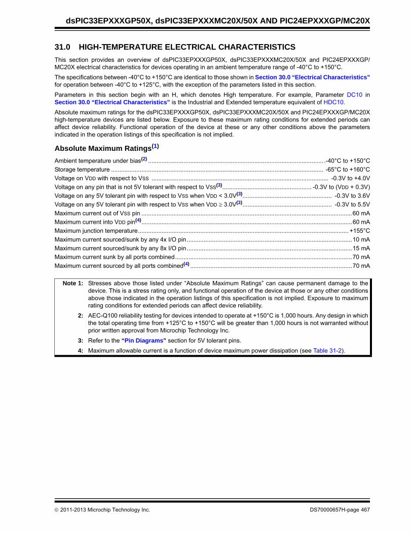
dsPIC33EPXXXGP50X, dsPIC33EPXXXMC20X/50X AND PIC24EPXXXGP/MC20X
31.0 HIGH-TEMPERATURE ELECTRICAL CHARACTERISTICS
This section provides an overview of dsPIC33EPXXXGP50X, dsPIC33EPXXXMC20X/50X and PIC24EPXXXGP/MC20X electrical characteristics for devices operating in an ambient temperature range of -40°C to +150°C.
The specifications between -40°C to +150°C are identical to those shown in Section 30.0 “Electrical Characteristics”for operation between -40°C to +125°C, with the exception of the parameters listed in this section.
Parameters in this section begin with an H, which denotes High temperature. For example, Parameter DC10 inSection 30.0 “Electrical Characteristics” is the Industrial and Extended temperature equivalent of HDC10.
Absolute maximum ratings for the dsPIC33EPXXXGP50X, dsPIC33EPXXXMC20X/50X and PIC24EPXXXGP/MC20Xhigh-temperature devices are listed below. Exposure to these maximum rating conditions for extended periods canaffect device reliability. Functional operation of the device at these or any other conditions above the parametersindicated in the operation listings of this specification is not implied.
Absolute Maximum Ratings(1)
Ambient temperature under bias(2) ........................................................................................................ .-40°C to +150°C
Storage temperature .............................................................................................................................. -65°C to +160°C
Voltage on VDD with respect to VSS ......................................................................................................... -0.3V to +4.0V
Voltage on any pin that is not 5V tolerant with respect to VSS(3)..................................................... -0.3V to (VDD + 0.3V)
Voltage on any 5V tolerant pin with respect to VSS when VDD < 3.0V(3)..................................................... -0.3V to 3.6V
Voltage on any 5V tolerant pin with respect to VSS when VDD 3.0V(3)..................................................... -0.3V to 5.5V
Maximum current out of VSS pin .............................................................................................................................60 mA
Maximum current into VDD pin(4).............................................................................................................................60 mA
Maximum junction temperature............................................................................................................................. +155°C
Maximum current sourced/sunk by any 4x I/O pin ..................................................................................................10 mA
Maximum current sourced/sunk by any 8x I/O pin ..................................................................................................15 mA
Maximum current sunk by all ports combined.........................................................................................................70 mA
Maximum current sourced by all ports combined(4) ................................................................................................70 mA
Note 1: Stresses above those listed under “Absolute Maximum Ratings” can cause permanent damage to thedevice. This is a stress rating only, and functional operation of the device at those or any other conditionsabove those indicated in the operation listings of this specification is not implied. Exposure to maximumrating conditions for extended periods can affect device reliability.
2: AEC-Q100 reliability testing for devices intended to operate at +150°C is 1,000 hours. Any design in whichthe total operating time from +125°C to +150°C will be greater than 1,000 hours is not warranted withoutprior written approval from Microchip Technology Inc.
3: Refer to the “Pin Diagrams” section for 5V tolerant pins.
4: Maximum allowable current is a function of device maximum power dissipation (see Table 31-2).
2011-2013 Microchip Technology Inc. DS70000657H-page 467

dsPIC33EPXXXGP50X, dsPIC33EPXXXMC20X/50X AND PIC24EPXXXGP/MC20X
31.1 High-Temperature DC Characteristics
TABLE 31-1: OPERATING MIPS VS. VOLTAGE
TABLE 31-2: THERMAL OPERATING CONDITIONS
TABLE 31-3: DC TEMPERATURE AND VOLTAGE SPECIFICATIONS
CharacteristicVDD Range(in Volts)
Temperature Range(in °C)
Max MIPS
dsPIC33EPXXXGP50X, dsPIC33EPXXXMC20X/50X and
PIC24EPXXXGP/MC20X
HDC5 3.0 to 3.6V(1) -40°C to +150°C 40
Note 1: Device is functional at VBORMIN < VDD < VDDMIN. Analog modules, such as the ADC, may have degraded performance. Device functionality is tested but not characterized.
Rating Symbol Min Typ Max Unit
High-Temperature Devices
Operating Junction Temperature Range TJ -40 — +155 °C
Operating Ambient Temperature Range TA -40 — +150 °C
Power Dissipation:Internal Chip Power Dissipation:
PINT = VDD x (IDD – IOH) PD PINT + PI/O WI/O Pin Power Dissipation:
I/O = ({VDD – VOH} x IOH) + (VOL x IOL)
Maximum Allowed Power Dissipation PDMAX (TJ – TA)/JA W
DC CHARACTERISTICSStandard Operating Conditions: 3.0V to 3.6V(unless otherwise stated)Operating temperature -40°C TA +150°C
Parameter No.
Symbol Characteristic Min Typ Max Units Conditions
Operating Voltage
HDC10 Supply Voltage
VDD — 3.0 3.3 3.6 V -40°C to +150°C
DS70000657H-page 468 2011-2013 Microchip Technology Inc.

dsPIC33EPXXXGP50X, dsPIC33EPXXXMC20X/50X AND PIC24EPXXXGP/MC20X
TABLE 31-4: DC CHARACTERISTICS: POWER-DOWN CURRENT (IPD)
TABLE 31-5: DC CHARACTERISTICS: IDLE CURRENT (IIDLE)
TABLE 31-6: DC CHARACTERISTICS: OPERATING CURRENT (IDD)
TABLE 31-7: DC CHARACTERISTICS: DOZE CURRENT (IDOZE)
DC CHARACTERISTICSStandard Operating Conditions: 3.0V to 3.6V(unless otherwise stated)Operating temperature -40°C TA +150°C
Parameter No.
Typical Max Units Conditions
Power-Down Current (IPD)
HDC60e 1400 2500 A +150°C 3.3V Base Power-Down Current(Notes 1, 3)
HDC61c 15 — A +150°C 3.3V Watchdog Timer Current: IWDT
(Notes 2, 4)
Note 1: Base IPD is measured with all peripherals and clocks shut down. All I/Os are configured as inputs and pulled to VSS. WDT, etc., are all switched off and VREGS (RCON<8>) = 1.
2: The current is the additional current consumed when the module is enabled. This current should be added to the base IPD current.
3: These currents are measured on the device containing the most memory in this family.
4: These parameters are characterized, but are not tested in manufacturing.
DC CHARACTERISTICSStandard Operating Conditions: 3.0V to 3.6V(unless otherwise stated)Operating temperature -40°C TA +150°C
Parameter No.
Typical Max Units Conditions
HDC44e 12 30 mA +150°C 3.3V 40 MIPS
DC CHARACTERISTICSStandard Operating Conditions: 3.0V to 3.6V(unless otherwise stated)Operating temperature -40°C TA +150°C
Parameter No.
Typical Max Units Conditions
HDC20 9 15 mA +150°C 3.3V 10 MIPS
HDC22 16 25 mA +150°C 3.3V 20 MIPS
HDC23 30 50 mA +150°C 3.3V 40 MIPS
DC CHARACTERISTICSStandard Operating Conditions: 3.0V to 3.6V(unless otherwise stated)Operating temperature -40°C TA +150°C
Parameter No.
Typical MaxDoze Ratio
Units Conditions
HDC72a 24 35 1:2 mA
+150°C 3.3V 40 MIPSHDC72f(1) 14 — 1:64 mA
HDC72g(1) 12 — 1:128 mA
Note 1: Parameters with Doze ratios of 1:64 and 1:128 are characterized, but are not tested in manufacturing.
2011-2013 Microchip Technology Inc. DS70000657H-page 469

dsPIC33EPXXXGP50X, dsPIC33EPXXXMC20X/50X AND PIC24EPXXXGP/MC20X
TABLE 31-8: DC CHARACTERISTICS: I/O PIN OUTPUT SPECIFICATIONS
DC CHARACTERISTICSStandard Operating Conditions: 3.0V to 3.6V(unless otherwise stated)Operating temperature -40°C TA +150°C
Param. Symbol Characteristic Min. Typ. Max. Units Conditions
HDO10 VOL Output Low Voltage4x Sink Driver Pins(2)
— — 0.4 V IOL 5 mA, VDD = 3.3V(Note 1)
Output Low Voltage8x Sink Driver Pins(3)
— — 0.4 V IOL 8 mA, VDD = 3.3V(Note 1)
HDO20 VOH Output High Voltage4x Source Driver Pins(2)
2.4 — — V IOH -10 mA, VDD = 3.3V(Note 1)
Output High Voltage8x Source Driver Pins(3)
2.4 — — V IOH 15 mA, VDD = 3.3V(Note 1)
HDO20A VOH1 Output High Voltage4x Source Driver Pins(2)
1.5 — — V IOH -3.9 mA, VDD = 3.3V(Note 1)
2.0 — — IOH -3.7 mA, VDD = 3.3V(Note 1)
3.0 — — IOH -2 mA, VDD = 3.3V(Note 1)
Output High Voltage8x Source Driver Pins(3)
1.5 — — V IOH -7.5 mA, VDD = 3.3V(Note 1)
2.0 — — IOH -6.8 mA, VDD = 3.3V(Note 1)
3.0 — — IOH -3 mA, VDD = 3.3V(Note 1)
Note 1: Parameters are characterized, but not tested.
2: Includes all I/O pins that are not 8x Sink Driver pins (see below).
3: Includes the following pins:For devices with less than 64 pins: RA3, RA4, RA9, RB<15:7> and RC3For 64-pin devices: RA4, RA9, RB<15:7>, RC3 and RC15
DS70000657H-page 470 2011-2013 Microchip Technology Inc.
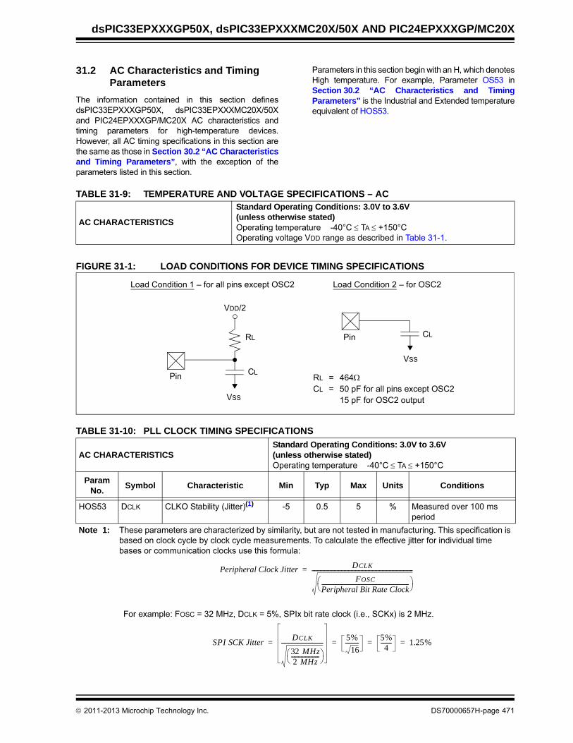
dsPIC33EPXXXGP50X, dsPIC33EPXXXMC20X/50X AND PIC24EPXXXGP/MC20X
31.2 AC Characteristics and Timing Parameters
The information contained in this section definesdsPIC33EPXXXGP50X, dsPIC33EPXXXMC20X/50Xand PIC24EPXXXGP/MC20X AC characteristics andtiming parameters for high-temperature devices.However, all AC timing specifications in this section arethe same as those in Section 30.2 “AC Characteristicsand Timing Parameters”, with the exception of theparameters listed in this section.
Parameters in this section begin with an H, which denotesHigh temperature. For example, Parameter OS53 inSection 30.2 “AC Characteristics and TimingParameters” is the Industrial and Extended temperatureequivalent of HOS53.
TABLE 31-9: TEMPERATURE AND VOLTAGE SPECIFICATIONS – AC
FIGURE 31-1: LOAD CONDITIONS FOR DEVICE TIMING SPECIFICATIONS
TABLE 31-10: PLL CLOCK TIMING SPECIFICATIONS
AC CHARACTERISTICS
Standard Operating Conditions: 3.0V to 3.6V(unless otherwise stated)Operating temperature -40°C TA +150°COperating voltage VDD range as described in Table 31-1.
AC CHARACTERISTICSStandard Operating Conditions: 3.0V to 3.6V(unless otherwise stated)Operating temperature -40°C TA +150°C
ParamNo.
Symbol Characteristic Min Typ Max Units Conditions
HOS53 DCLK CLKO Stability (Jitter)(1) -5 0.5 5 % Measured over 100 ms period
Note 1: These parameters are characterized by similarity, but are not tested in manufacturing. This specification is based on clock cycle by clock cycle measurements. To calculate the effective jitter for individual time bases or communication clocks use this formula:
VDD/2
CL
RL
Pin
Pin
VSS
VSS
CL
RL = 464CL = 50 pF for all pins except OSC2
15 pF for OSC2 output
Load Condition 1 – for all pins except OSC2 Load Condition 2 – for OSC2
Peripheral Clock Jitter DCLK
FOSC
Peripheral Bit Rate Clock--------------------------------------------------------------
------------------------------------------------------------------------=
For example: FOSC = 32 MHz, DCLK = 5%, SPIx bit rate clock (i.e., SCKx) is 2 MHz.
SPI SCK JitterDCLK
32 MHz2 MHz
--------------------
------------------------------5%
16----------
5%4
-------- 1.25%= = = =
2011-2013 Microchip Technology Inc. DS70000657H-page 471

dsPIC33EPXXXGP50X, dsPIC33EPXXXMC20X/50X AND PIC24EPXXXGP/MC20X
TABLE 31-11: INTERNAL RC ACCURACY
AC CHARACTERISTICSStandard Operating Conditions: 3.0V to 3.6V (unless otherwise stated)Operating temperature -40°C TA +150°C
ParamNo.
Characteristic Min Typ Max Units Conditions
LPRC @ 32.768 kHz(1,2)
HF21 LPRC -30 — +30 % -40°C TA +150°C VDD = 3.0-3.6V
Note 1: Change of LPRC frequency as VDD changes.
2: LPRC accuracy impacts the Watchdog Timer Time-out Period (TWDT). See Section 27.5 “Watchdog Timer (WDT)” for more information.
DS70000657H-page 472 2011-2013 Microchip Technology Inc.

dsPIC33EPXXXGP50X, dsPIC33EPXXXMC20X/50X AND PIC24EPXXXGP/MC20X
TABLE 31-12: ADC MODULE SPECIFICATIONS (12-BIT MODE)
TABLE 31-13: ADC MODULE SPECIFICATIONS (10-BIT MODE)
AC CHARACTERISTICSStandard Operating Conditions: 3.0V to 3.6V (unless otherwise stated)Operating temperature -40°C TA +150°C
Param No.
Symbol Characteristic Min Typ Max Units Conditions
ADC Accuracy (12-Bit Mode)(1)
HAD20a Nr Resolution(3) 12 Data Bits bits
HAD21a INL Integral Nonlinearity -5.5 — 5.5 LSb VINL = AVSS = VREFL = 0V, AVDD = VREFH = 3.6V
HAD22a DNL Differential Nonlinearity -1 — 1 LSb VINL = AVSS = VREFL = 0V, AVDD = VREFH = 3.6V
HAD23a GERR Gain Error -10 — 10 LSb VINL = AVSS = VREFL = 0V, AVDD = VREFH = 3.6V
HAD24a EOFF Offset Error -5 — 5 LSb VINL = AVSS = VREFL = 0V, AVDD = VREFH = 3.6V
Dynamic Performance (12-Bit Mode)(2)
HAD33a FNYQ Input Signal Bandwidth — — 200 kHz
Note 1: These parameters are characterized, but are tested at 20 ksps only.
2: These parameters are characterized by similarity, but are not tested in manufacturing.
3: Injection currents > | 0 | can affect the ADC results by approximately 4-6 counts.
AC CHARACTERISTICSStandard Operating Conditions: 3.0V to 3.6V (unless otherwise stated)Operating temperature -40°C TA +150°C
Param No.
Symbol Characteristic Min Typ Max Units Conditions
ADC Accuracy (10-Bit Mode)(1)
HAD20b Nr Resolution(3) 10 Data Bits bits
HAD21b INL Integral Nonlinearity -1.5 — 1.5 LSb VINL = AVSS = VREFL = 0V, AVDD = VREFH = 3.6V
HAD22b DNL Differential Nonlinearity -0.25 — 0.25 LSb VINL = AVSS = VREFL = 0V, AVDD = VREFH = 3.6V
HAD23b GERR Gain Error -2.5 — 2.5 LSb VINL = AVSS = VREFL = 0V, AVDD = VREFH = 3.6V
HAD24b EOFF Offset Error -1.25 — 1.25 LSb VINL = AVSS = VREFL = 0V, AVDD = VREFH = 3.6V
Dynamic Performance (10-Bit Mode)(2)
HAD33b FNYQ Input Signal Bandwidth — — 400 kHz
Note 1: These parameters are characterized, but are tested at 20 ksps only.
2: These parameters are characterized by similarity, but are not tested in manufacturing.
3: Injection currents > | 0 | can affect the ADC results by approximately 4-6 counts.
2011-2013 Microchip Technology Inc. DS70000657H-page 473
dsPIC33EPXXXGP50X, dsPIC33EPXXXMC20X/50X AND PIC24EPXXXGP/MC20X
NOTES:
DS70000657H-page 474 2011-2013 Microchip Technology Inc.

2
01
1-2
01
3 M
icroch
ip T
ech
no
log
y Inc.
DS
70
00
06
57
H-p
ag
e 4
75
ds
PIC
33E
PX
XX
GP
50X
, ds
PIC
33E
PX
XX
MC
20X
/50X
AN
D P
IC2
4EP
XX
XG
P/M
C2
0X
32
FIG
FIG
VER PINS
VER PINS
N provided for design guidance purposesd may be outside the specified operating
VOL (V)
2.00 2.50 3.00 3.50 4.00
VOL (V)
3V
3.3V
3.6V
Absolute Maximum
VOL (V)8X
2.00 2.50 3.00 3.50 4.00
VOL (V)8X
3V
3.3V
3.6V
Absolute Maximum
.0 DC AND AC DEVICE CHARACTERISTICS GRAPHS
URE 32-1: VOH – 4x DRIVER PINS
URE 32-2: VOH – 8x DRIVER PINS
FIGURE 32-3: VOL – 4x DRI
FIGURE 32-4: VOL – 8x DRI
ote: The graphs provided following this note are a statistical summary based on a limited number of samples and areonly. The performance characteristics listed herein are not tested or guaranteed. In some graphs, the data presenterange (e.g., outside specified power supply range) and therefore, outside the warranted range.
-0.050
-0.045
-0.040
-0.035
-0.030
-0.025
-0.020IOH
(A)
VOH (V)-0.050
-0.045
-0.040
-0.035
-0.030
-0.025
-0.020
-0.015
-0.010
-0.005
0.0000.00 0.50 1.00 1.50 2.00 2.50 3.00 3.50 4.00
IOH
(A)
VOH (V)
3V
3.3V
3.6V
Absolute Maximum
-0.080
-0.070
-0.060
-0.050
-0.040
0 030
IOH(A)
VOH (V)-0.080
-0.070
-0.060
-0.050
-0.040
-0.030
-0.020
-0.010
0.0000.00 0.50 1.00 1.50 2.00 2.50 3.00 3.50 4.00
IOH(A)
VOH (V)
3V
3.3V
3.6V
Absolute Maximum
0.0150.0200.0250.0300.0350.0400.0450.050
IOH
(A)
0.0000.0050.0100.0150.0200.0250.0300.0350.0400.0450.050
0.00 0.50 1.00 1.50
IOH
(A)
0 020
0.030
0.040
0.050
0.060
0.070
0.080
IOH
(A)
0.000
0.010
0.020
0.030
0.040
0.050
0.060
0.070
0.080
0.00 0.50 1.00 1.50
IOH
(A)

ds
PIC
33E
PX
XX
GP
50X
, dsP
IC33
EP
XX
XM
C20
X/5
0X A
ND
PIC
24E
PX
XX
GP
/MC
20X
DS
70
00
06
57
H-p
ag
e 4
76
2
01
1-2
01
3 M
icroch
ip T
ech
no
log
y Inc.
IDOZE CURRENT @ VDD = 3.3V
IIDLE CURRENT @ VDD = 3.3V
1:8 1:16 1:32 1:64 1:128
Doze Ratio
30 40 50 60 70MIPS
IIDLE (EC+PLL)
FIGURE 32-5: TYPICAL IPD CURRENT @ VDD = 3.3V
FIGURE 32-6: TYPICAL/MAXIMUM IDD CURRENT @ VDD = 3.3V
FIGURE 32-7: TYPICAL
FIGURE 32-8: TYPICAL
200.00
300.00
400.00
500.00
600.00
700.00
800.00
IPD
Cur
rent
(µA)
0.00
100.00
200.00
300.00
400.00
500.00
600.00
700.00
800.00
-40 -30 -20 -10 0 10 20 30 40 50 60 70 80 90 100 110 120
IPD
Cur
rent
(µA)
Temperature (Celsius)
0
10
20
30
40
50
60
70
0 10 20 30 40 50 60 70 80
Typ.
Max.
MIPS
IDD
(m
A)
15.00
20.00
25.00
30.00
35.00
40.00
45.00
OZE
Cur
rent
(mA)
0.00
5.00
10.00
15.00
20.00
25.00
30.00
35.00
40.00
45.00
1:1 1:2 1:4
IDO
ZEC
urre
nt (m
A)10.00
15.00
20.00
25.00
IDLE
Cur
rent
(mA
)
0.00
5.00
10.00
15.00
20.00
25.00
0 10 20
IIDLE
Cur
rent
(mA
)
IIDLE (EC)
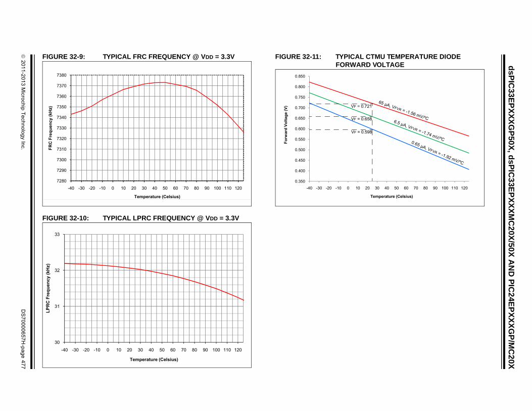
2
01
1-2
01
3 M
icroch
ip T
ech
no
log
y Inc.
DS
70
00
06
57
H-p
ag
e 4
77
ds
PIC
33E
PX
XX
GP
50X
, ds
PIC
33E
PX
XX
MC
20X
/50X
AN
D P
IC2
4EP
XX
XG
P/M
C2
0X
FIG
FIG
U TEMPERATURE DIODE OLTAGE
0 40 50 60 70 80 90 100 110 120 130
mperature (Celsius)
65 µA, VFVR = -1.56 mV/ºC6.5 µA, VFVR = -1.74 mV/ºC
0.65 µA, VFVR = -1.92 mV/ºC
URE 32-9: TYPICAL FRC FREQUENCY @ VDD = 3.3V
URE 32-10: TYPICAL LPRC FREQUENCY @ VDD = 3.3V
FIGURE 32-11: TYPICAL CTMFORWARD V
7310
7320
7330
7340
7350
7360
7370
7380
FRC
Fre
quen
cy (k
Hz)
7280
7290
7300
7310
7320
7330
7340
7350
7360
7370
7380
-40 -30 -20 -10 0 10 20 30 40 50 60 70 80 90 100 110 120
FRC
Fre
quen
cy (k
Hz)
Temperature (Celsius)
31
32
33
LPR
C F
requ
ency
(kH
z)
30
31
32
33
-40 -30 -20 -10 0 10 20 30 40 50 60 70 80 90 100 110 120
LPR
C F
requ
ency
(kH
z)
Temperature (Celsius)
0.550
0.600
0.650
0.700
0.750
0.800
0.850
Forw
ard
Volta
ge (V
)
0.350
0.400
0.450
0.500
0.550
0.600
0.650
0.700
0.750
0.800
0.850
-40 -30 -20 -10 0 10 20 3
Forw
ard
Volta
ge (V
)
Te
VF = 0.598
VF = 0.658
VF = 0.721

dsPIC33EPXXXGP50X, dsPIC33EPXXXMC20X/50X AND PIC24EPXXXGP/MC20X
NOTES:
DS70000657H-page 478 2011-2013 Microchip Technology Inc.

dsPIC33EPXXXGP50X, dsPIC33EPXXXMC20X/50X AND PIC24EPXXXGP/MC20X
33.0 PACKAGING INFORMATION
33.1 Package Marking Information
Legend: XX...X Customer-specific informationY Year code (last digit of calendar year)YY Year code (last 2 digits of calendar year)WW Week code (week of January 1 is week ‘01’)NNN Alphanumeric traceability code Pb-free JEDEC designator for Matte Tin (Sn)* This package is Pb-free. The Pb-free JEDEC designator ( )
can be found on the outer packaging for this package.
Note: In the event the full Microchip part number cannot be marked on one line, it willbe carried over to the next line, thus limiting the number of availablecharacters for customer-specific information.
3e
3e
28-Lead SPDIP
XXXXXXXXXXXXXXXXXXXXXXXXXXXXXXXXXX
YYWWNNN
Example
dsPIC33EP64GP
1310017502-I/SP 3e
28-Lead SOIC (.300”)
XXXXXXXXXXXXXXXXXXXXXXXXXXXXXXXXXXXXXXXXXXXXXXXXXXXXXXXXXXXX
YYWWNNN
Example
dsPIC33EP64GP
1310017502-I/SO 3e
28-Lead SSOP
XXXXXXXXXXXXXXXXXXXXXXXX
YYWWNNN
Example
dsPIC33EP64GP502-I/SS
13100173e
XXXXXXXX
28-Lead QFN-S (6x6x0.9 mm)
XXXXXXXXYYWWNNN
33EP64GP
Example
502-I/MM1310017
2011-2013 Microchip Technology Inc. DS70000657H-page 479

dsPIC33EPXXXGP50X, dsPIC33EPXXXMC20X/50X AND PIC24EPXXXGP/MC20X
33.1 Package Marking Information (Continued)
XXXXXXXXXX
36-Lead VTLA (TLA)
XXXXXXXXXXXXXXXXXXXX
YYWWNNN
Example
XXXXXXXXXX
44-Lead VTLA (TLA)
XXXXXXXXXXXXXXXXXXXX
YYWWNNN
504-I/TL
1310017
33EP64GP3e
Example
504-I/TL
1310017
33EP64GP3e
44-Lead TQFP
XXXXXXXXXXXXXXXXXXXXXXXXXXXXXX
YYWWNNN
Example
33EP64GP504-I/PT
1310017
3e
XXXXXXXXXXX
44-Lead QFN (8x8x0.9 mm)
XXXXXXXXXXXXXXXXXXXXXX
YYWWNNN
33EP64GP
Example
504-I/ML1310017
3e
DS70000657H-page 480 2011-2013 Microchip Technology Inc.

dsPIC33EPXXXGP50X, dsPIC33EPXXXMC20X/50X AND PIC24EPXXXGP/MC20X
33.1 Package Marking Information (Continued)
XXXXXXXXXXX
64-Lead QFN (9x9x0.9 mm)
XXXXXXXXXXXXXXXXXXXXXX
YYWWNNN
dsPIC33EP
Example
64GP506
13100173e-I/MR
64-Lead TQFP (10x10x1 mm)
XXXXXXXXXXXXXXXXXXXXXXXXXXXXXX
YYWWNNN
Example
dsPIC33EP64GP506
1310017-I/PT 3e
XXXXXXXXXXX
48-Lead UQFN (6x6x0.5 mm)
XXXXXXXXXXXXXXXXXXXXXX
YYWWNNN
33EP64GP
Example
504-I/MV1310017
3e
2011-2013 Microchip Technology Inc. DS70000657H-page 481

dsPIC33EPXXXGP50X, dsPIC33EPXXXMC20X/50X AND PIC24EPXXXGP/MC20X
33.2 Package Details
��������� ������������� ��� ��������������������
!����"�� ������ �!"�����#�$�%��&"��'��� ��(�)"&�'"!&�)�����&�#�*�&����&�����&���#������� +������%����&�,����&��!&���-� ��'��!��!�����#�.��#��&�����"#��'�#�%��!����&"!��!����#�%��!����&"!��!�!������&��$���#�����/����!�#���� ��'��!��������#�&���������������.�0������
1�,2 1�!�����'��!���� ���&��������$��&� ��"��!�*��*�&�"&�&������!�
!���" 3�&���'!&��"��&����4����#�*���!(�����!��!���&��������������4�����������%���&������&�#��&��&&�255***�'��������'5���4�����
6��&! �7,8.���'��!���9�'�&! ��7 7:� ��;
7"')��%����! 7 �<��&�� � �����1�, ��&����&��������� � = = ������#�#����4���� ���4��!! �� ���� ��-� ����1�!��&����&��������� �� ���� = =��"�#��&���"�#��>�#&� . ���� �-�� �--���#�#����4����>�#&� .� ���� ��<� ����: �����9���&� � ��-�� ��-?� ����� ���&����&��������� 9 ���� ��-� ����9��#� ���4��!! � ���< ���� ����6����9��#�>�#&� )� ���� ���� ����9*��9��#�>�#&� ) ���� ���< ����: ������*����������+ �1 = = ��-�
NOTE 1
N
1 2
D
E1
eB
c
E
L
A2
eb
b1A1
A
3
������� ������� ��*��� ,������1
DS70000657H-page 482 2011-2013 Microchip Technology Inc.

dsPIC33EPXXXGP50X, dsPIC33EPXXXMC20X/50X AND PIC24EPXXXGP/MC20X
Note: For the most current package drawings, please see the Microchip Packaging Specification located at
http://www.microchip.com/packaging
2011-2013 Microchip Technology Inc. DS70000657H-page 483
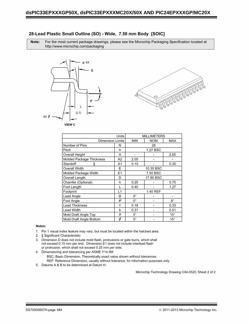
dsPIC33EPXXXGP50X, dsPIC33EPXXXMC20X/50X AND PIC24EPXXXGP/MC20X
Note: For the most current package drawings, please see the Microchip Packaging Specification located at
http://www.microchip.com/packaging
DS70000657H-page 484 2011-2013 Microchip Technology Inc.

dsPIC33EPXXXGP50X, dsPIC33EPXXXMC20X/50X AND PIC24EPXXXGP/MC20X
Note: For the most current package drawings, please see the Microchip Packaging Specification located at
http://www.microchip.com/packaging
2011-2013 Microchip Technology Inc. DS70000657H-page 485
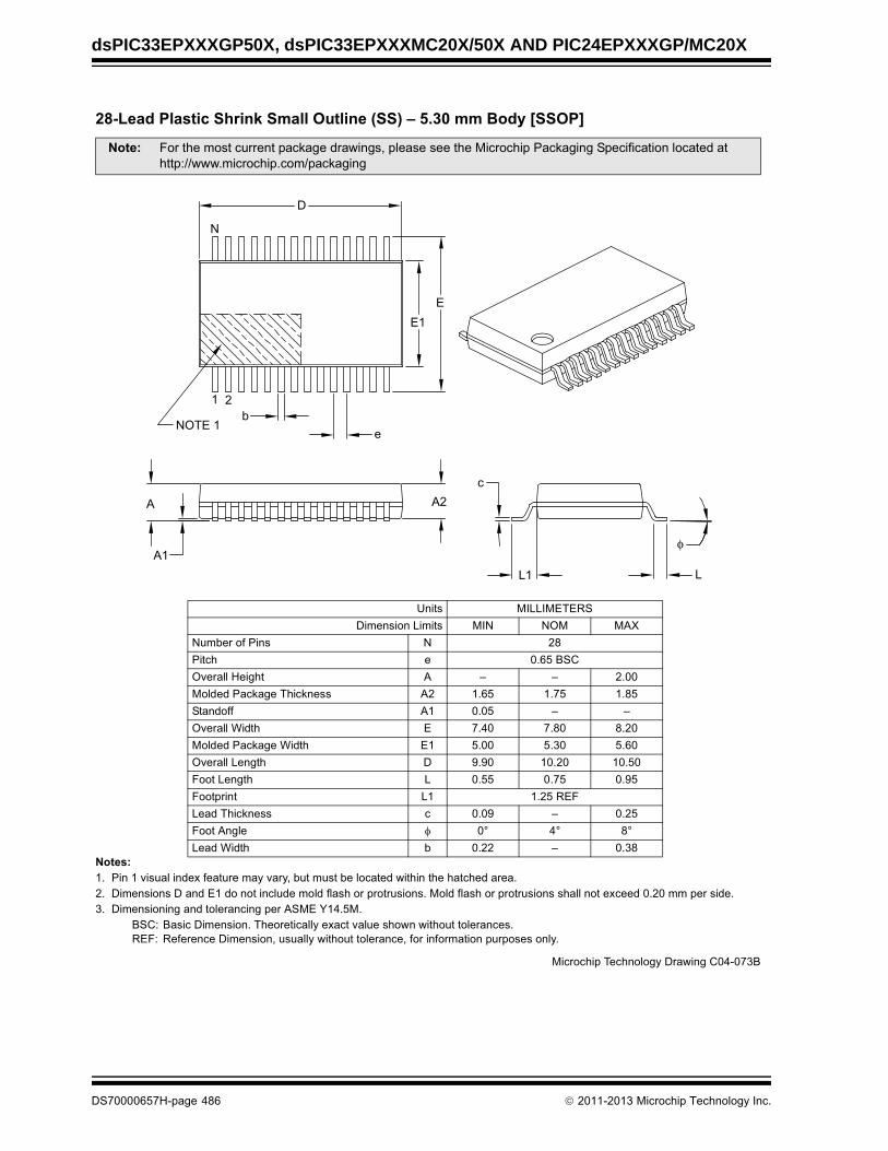
dsPIC33EPXXXGP50X, dsPIC33EPXXXMC20X/50X AND PIC24EPXXXGP/MC20X
��������������#$� �����%���� ����&'���������%�
!����"�� ������ �!"�����#�$�%��&"��'��� ��(�)"&�'"!&�)�����&�#�*�&����&�����&���#������� ��'��!��!�����#�.��#��&�����"#��'�#�%��!����&"!��!����#�%��!����&"!��!�!������&��$���#������''����!�#��-� ��'��!��������#�&���������������.�0������
1�,2 1�!�����'��!���� ���&��������$��&� ��"��!�*��*�&�"&�&������!��.32 ��%��������'��!��(�"!"�����*�&�"&�&������(�%���%'�&����"�!�!�����
!���" 3�&���'!&��"��&����4����#�*���!(�����!��!���&��������������4�����������%���&������&�#��&��&&�255***�'��������'5���4�����
6��&! ��99��. .����'��!���9�'�&! ��7 7:� ��;
7"')��%����! 7 �<��&�� � ��?��1�,: �����8����& � = = ������#�#����4���� ���4��!! �� ��?� ���� ��<��&��#%%� �� ���� = =: �����>�#&� . ���� ��<� <�����#�#����4����>�#&� .� ���� ��-� ��?�: �����9���&� � ���� ����� �����3&�9���&� 9 ���� ���� ����3&���& 9� ������.39��#� ���4��!! � ���� = ����3&������ � �@ �@ <@9��#�>�#&� ) ���� = ��-<
LL1
c
A2
A1
A
E
E1
D
N
1 2
NOTE 1b
e
φ
������� ������� ��*��� ,�����-1
DS70000657H-page 486 2011-2013 Microchip Technology Inc.
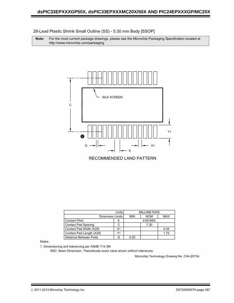
dsPIC33EPXXXGP50X, dsPIC33EPXXXMC20X/50X AND PIC24EPXXXGP/MC20X
Note: For the most current package drawings, please see the Microchip Packaging Specification located at
http://www.microchip.com/packaging
2011-2013 Microchip Technology Inc. DS70000657H-page 487
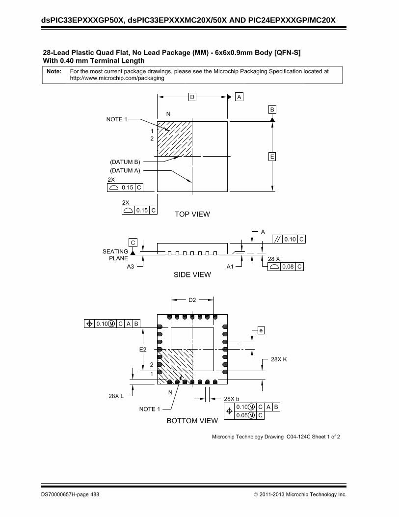
dsPIC33EPXXXGP50X, dsPIC33EPXXXMC20X/50X AND PIC24EPXXXGP/MC20X
DS70000657H-page 488 2011-2013 Microchip Technology Inc.

dsPIC33EPXXXGP50X, dsPIC33EPXXXMC20X/50X AND PIC24EPXXXGP/MC20X
2011-2013 Microchip Technology Inc. DS70000657H-page 489

dsPIC33EPXXXGP50X, dsPIC33EPXXXMC20X/50X AND PIC24EPXXXGP/MC20X
��������������(���)���*!����������+��,,��-.-.�'/�������()!� 0��#�'1���2� ������ +�#
!���" 3�&���'!&��"��&����4����#�*���!(�����!��!���&��������������4�����������%���&������&�#��&��&&�255***�'��������'5���4�����
DS70000657H-page 490 2011-2013 Microchip Technology Inc.

dsPIC33EPXXXGP50X, dsPIC33EPXXXMC20X/50X AND PIC24EPXXXGP/MC20X
2011-2013 Microchip Technology Inc. DS70000657H-page 491

dsPIC33EPXXXGP50X, dsPIC33EPXXXMC20X/50X AND PIC24EPXXXGP/MC20X
DS70000657H-page 492 2011-2013 Microchip Technology Inc.
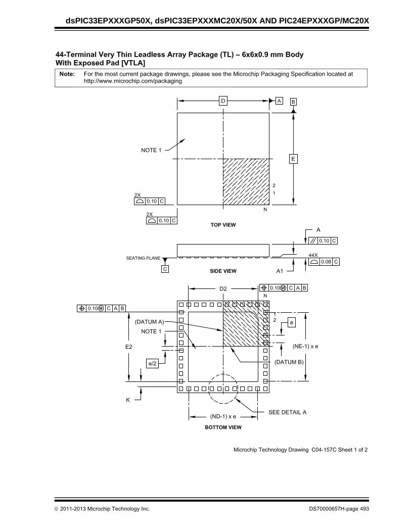
dsPIC33EPXXXGP50X, dsPIC33EPXXXMC20X/50X AND PIC24EPXXXGP/MC20X
2011-2013 Microchip Technology Inc. DS70000657H-page 493

dsPIC33EPXXXGP50X, dsPIC33EPXXXMC20X/50X AND PIC24EPXXXGP/MC20X
DS70000657H-page 494 2011-2013 Microchip Technology Inc.

dsPIC33EPXXXGP50X, dsPIC33EPXXXMC20X/50X AND PIC24EPXXXGP/MC20X
11������������3#� (���)���4�����3��5�.5�.5������*�'�����3()�
!����"�� ������ �!"�����#�$�%��&"��'��� ��(�)"&�'"!&�)�����&�#�*�&����&�����&���#������� ,��'%�!��&����!�����&����A�!�B��'��� ���-� ��'��!��!������#�.��#��&�����"#��'�#�%��!����&"!��!����#�%��!����&"!��!�!������&��$���#������''����!�#���� ��'��!��������#�&���������������.�0������
1�,2 1�!�����'��!���� ���&��������$��&� ��"��!�*��*�&�"&�&������!��.32 ��%��������'��!��(�"!"�����*�&�"&�&������(�%���%'�&����"�!�!�����
!���" 3�&���'!&��"��&����4����#�*���!(�����!��!���&��������������4�����������%���&������&�#��&��&&�255***�'��������'5���4�����
6��&! ��99��. .����'��!���9�'�&! ��7 7:� ��;
7"')��%�9��#! 7 ��9��#���&�� � ��<��1�,: �����8����& � = = ������#�#����4���� ���4��!! �� ���� ���� �����&��#%%�� �� ���� = ����3&�9���&� 9 ���� ��?� ����3&���& 9� ������.33&������ � �@ -��@ �@: �����>�#&� . ������1�,: �����9���&� � ������1�,��#�#����4����>�#&� .� ������1�,��#�#����4����9���&� �� ������1�,9��#� ���4��!! � ���� = ����9��#�>�#&� ) ��-� ��-� ������#���%&������� � � ��@ ��@ �-@��#���%&�������1&&' � ��@ ��@ �-@
A
E
E1
D
D1
e
b
NOTE 1NOTE 2
N
1 2 3
c
A1L
A2L1
α
φ
β
������� ������� ��*��� ,�����?1
2011-2013 Microchip Technology Inc. DS70000657H-page 495

dsPIC33EPXXXGP50X, dsPIC33EPXXXMC20X/50X AND PIC24EPXXXGP/MC20X
Note: For the most current package drawings, please see the Microchip Packaging Specification located at
http://www.microchip.com/packaging
DS70000657H-page 496 2011-2013 Microchip Technology Inc.
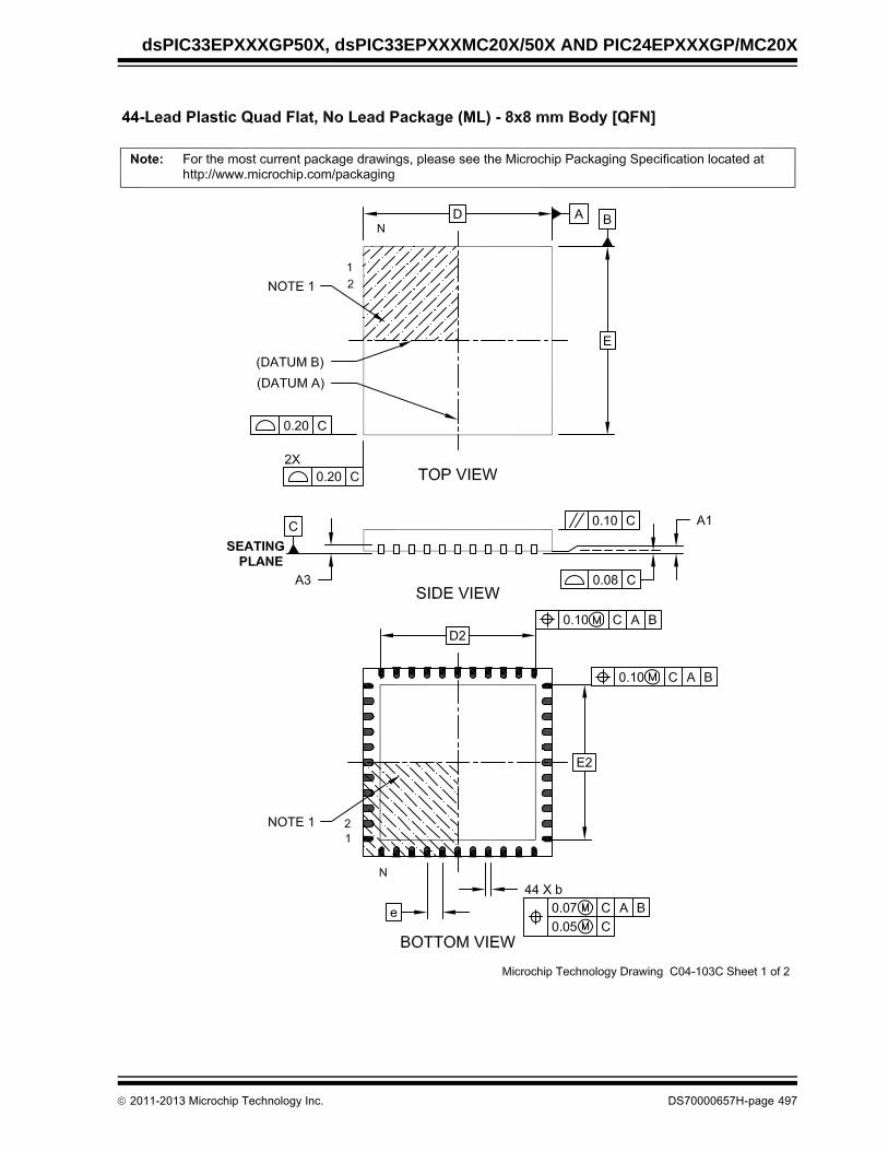
dsPIC33EPXXXGP50X, dsPIC33EPXXXMC20X/50X AND PIC24EPXXXGP/MC20X
2011-2013 Microchip Technology Inc. DS70000657H-page 497

dsPIC33EPXXXGP50X, dsPIC33EPXXXMC20X/50X AND PIC24EPXXXGP/MC20X
DS70000657H-page 498 2011-2013 Microchip Technology Inc.
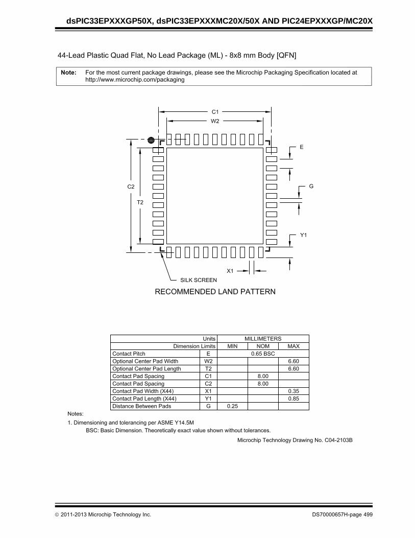
dsPIC33EPXXXGP50X, dsPIC33EPXXXMC20X/50X AND PIC24EPXXXGP/MC20X
2011-2013 Microchip Technology Inc. DS70000657H-page 499

dsPIC33EPXXXGP50X, dsPIC33EPXXXMC20X/50X AND PIC24EPXXXGP/MC20X
Note: For the most current package drawings, please see the Microchip Packaging Specification located at
http://www.microchip.com/packaging
DS70000657H-page 500 2011-2013 Microchip Technology Inc.

dsPIC33EPXXXGP50X, dsPIC33EPXXXMC20X/50X AND PIC24EPXXXGP/MC20X
Note: For the most current package drawings, please see the Microchip Packaging Specification located at
http://www.microchip.com/packaging
2011-2013 Microchip Technology Inc. DS70000657H-page 501

dsPIC33EPXXXGP50X, dsPIC33EPXXXMC20X/50X AND PIC24EPXXXGP/MC20X
DS70000657H-page 502 2011-2013 Microchip Technology Inc.

dsPIC33EPXXXGP50X, dsPIC33EPXXXMC20X/50X AND PIC24EPXXXGP/MC20X
Note: For the most current package drawings, please see the Microchip Packaging Specification located at
http://www.microchip.com/packaging
2011-2013 Microchip Technology Inc. DS70000657H-page 503

dsPIC33EPXXXGP50X, dsPIC33EPXXXMC20X/50X AND PIC24EPXXXGP/MC20X
Note: For the most current package drawings, please see the Microchip Packaging Specification located at
http://www.microchip.com/packaging
DS70000657H-page 504 2011-2013 Microchip Technology Inc.
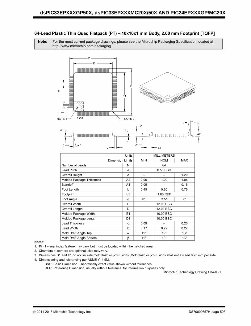
dsPIC33EPXXXGP50X, dsPIC33EPXXXMC20X/50X AND PIC24EPXXXGP/MC20X
64-Lead Plastic Thin Quad Flatpack (PT) – 10x10x1 mm Body, 2.00 mm Footprint [TQFP]
Notes:1. Pin 1 visual index feature may vary, but must be located within the hatched area.
2. Chamfers at corners are optional; size may vary.
3. Dimensions D1 and E1 do not include mold flash or protrusions. Mold flash or protrusions shall not exceed 0.25 mm per side.
4. Dimensioning and tolerancing per ASME Y14.5M.
BSC: Basic Dimension. Theoretically exact value shown without tolerances.
REF: Reference Dimension, usually without tolerance, for information purposes only.
Note: For the most current package drawings, please see the Microchip Packaging Specification located at
http://www.microchip.com/packaging
Units MILLIMETERS
Dimension Limits MIN NOM MAX
Number of Leads N 64
Lead Pitch e 0.50 BSC
Overall Height A – – 1.20
Molded Package Thickness A2 0.95 1.00 1.05
Standoff A1 0.05 – 0.15
Foot Length L 0.45 0.60 0.75
Footprint L1 1.00 REF
Foot Angle φ 0° 3.5° 7°
Overall Width E 12.00 BSC
Overall Length D 12.00 BSC
Molded Package Width E1 10.00 BSC
Molded Package Length D1 10.00 BSC
Lead Thickness c 0.09 – 0.20
Lead Width b 0.17 0.22 0.27
Mold Draft Angle Top α 11° 12° 13°
Mold Draft Angle Bottom β 11° 12° 13°
D
D1
E
E1
e
b
N
NOTE 1 1 2 3 NOTE 2
c
L
A1
L1
A2
A
φ
β
α
Microchip Technology Drawing C04-085B
2011-2013 Microchip Technology Inc. DS70000657H-page 505

dsPIC33EPXXXGP50X, dsPIC33EPXXXMC20X/50X AND PIC24EPXXXGP/MC20X
Note: For the most current package drawings, please see the Microchip Packaging Specification located at
http://www.microchip.com/packaging
DS70000657H-page 506 2011-2013 Microchip Technology Inc.

dsPIC33EPXXXGP50X, dsPIC33EPXXXMC20X/50X AND PIC24EPXXXGP/MC20X
APPENDIX A: REVISION HISTORY
Revision A (April 2011)
This is the initial released version of the document.
Revision B (July 2011)
This revision includes minor typographical andformatting changes throughout the data sheet text.
All other major changes are referenced by theirrespective section in Table A-1.
TABLE A-1: MAJOR SECTION UPDATES
Section Name Update Description
“High-Performance, 16-bit Digital Signal Controllers and Microcontrollers”
Changed all pin diagrams references of VLAP to TLA.
Section 4.0 “Memory Organization”
Updated the All Resets values for CLKDIV and PLLFBD in the System Control Register Map (see Table 4-35).
Section 5.0 “Flash Program Memory”
Updated “one word” to “two words” in the first paragraph of Section 5.2 “RTSP Operation”.
Section 9.0 “Oscillator Configuration”
Updated the PLL Block Diagram (see Figure 9-2).
Updated the Oscillator Mode, Fast RC Oscillator (FRC) with divide-by-N and PLL (FRCPLL), by changing (FRCDIVN + PLL) to (FRCPLL).
Changed (FRCDIVN + PLL) to (FRCPLL) for COSC<2:0> = 001 and NOSC<2:0> = 001 in the Oscillator Control Register (see Register 9-1).
Changed the POR value from 0 to 1 for the DOZE<1:0> bits, from 1 to 0 for the FRCDIV<0> bit, and from 0 to 1 for the PLLPOST<0> bit; Updated the default definitions for the DOZE<2:0> and FRCDIV<2:0> bits and updated all bit definitions for the PLLPOST<1:0> bits in the Clock Divisor Register (see Register 9-2).
Changed the POR value from 0 to 1 for the PLLDIV<5:4> bits and updated the default definitions for all PLLDIV<8:0> bits in the PLL Feedback Division Register (see Register 9-2).
Section 22.0 “Charge Time Measurement Unit (CTMU)”
Updated the bit definitions for the IRNG<1:0> bits in the CTMU Current Control Register (see Register 22-3).
Section 25.0 “Op amp/Comparator Module”
Updated the voltage reference block diagrams (see Figure 25-1 and Figure 25-2).
2011-2013 Microchip Technology Inc. DS70000657H-page 507

dsPIC33EPXXXGP50X, dsPIC33EPXXXMC20X/50X AND PIC24EPXXXGP/MC20X
Section 30.0 “Electrical Characteristics”
Removed Voltage on VCAP with respect to Vss and added Note 5 in Absolute Maximum Ratings(1).
Removed Parameter DC18 (VCORE) and Note 3 from the DC Temperature and Voltage Specifications (see Table 30-4).
Updated Note 1 in the DC Characteristics: Operating Current (IDD) (see Table 30-6).
Updated Note 1 in the DC Characteristics: Idle Current (IIDLE) (see Table 30-7).
Changed the Typical values for Parameters DC60a-DC60d and updated Note 1 in the DC Characteristics: Power-down Current (IPD) (see Table 30-8).
Updated Note 1 in the DC Characteristics: Doze Current (IDOZE) (see Table 30-9).
Updated Note 2 in the Electrical Characteristics: BOR (see Table 30-12).
Updated Parameters CM20 and CM31, and added Parameters CM44 and CM45 in the AC/DC Characteristics: Op amp/Comparator (see Table 30-14).
Added the Op amp/Comparator Reference Voltage Settling Time Specifications (see Table 30-15).
Added Op amp/Comparator Voltage Reference DC Specifications (see Table 30-16).
Updated Internal FRC Accuracy Parameter F20a (see Table 30-21).
Updated the Typical value and Units for Parameter CTMUI1, and added Parameters CTMUI4, CTMUFV1, and CTMUFV2 to the CTMU Current Source Specifications (see Table 30-55).
Section 31.0 “Packaging Information”
Updated packages by replacing references of VLAP with TLA.
“Product Identification System”
Changed VLAP to TLA.
TABLE A-1: MAJOR SECTION UPDATES (CONTINUED)
Section Name Update Description
DS70000657H-page 508 2011-2013 Microchip Technology Inc.

dsPIC33EPXXXGP50X, dsPIC33EPXXXMC20X/50X AND PIC24EPXXXGP/MC20X
Revision C (December 2011)
This revision includes typographical and formattingchanges throughout the data sheet text.
In addition, where applicable, new sections were addedto each peripheral chapter that provide information andlinks to related resources, as well as helpful tips. Forexamples, see Section 20.1 “UART Helpful Tips”and Section 3.6 “CPU Resources”.
All occurrences of TLA were updated to VTLAthroughout the document, with the exception of the pindiagrams (updated diagrams were not available at timeof publication).
A new chapter, Section 31.0 “DC and AC DeviceCharacteristics Graphs”, was added.
All other major changes are referenced by theirrespective section in Table A-2.
TABLE A-2: MAJOR SECTION UPDATES
Section Name Update Description
“16-bit Microcontrollers and Digital Signal Controllers (up to 256-Kbyte Flash and 32-Kbyte SRAM) with High-Speed PWM, Op amps, and Advanced Analog”
The content on the first page of this section was extensively reworked to provide the reader with the key features and functionality of this device family in an “at-a-glance” format.
Section 1.0 “Device Overview”
Updated the dsPIC33EPXXXGP50X, dsPIC33EPXXXMC20X/50X, and PIC24EPXXXGP/MC20X Block Diagram (see Figure 1-1), which now contains a CPU block and a reference to the CPU diagram.
Updated the description and Note references in the Pinout I/O Descriptions for these pins: C1IN2-, C2IN2-, C3IN2-, OA1OUT, OA2OUT, and OA3OUT (see Table 1-1).
Section 2.0 “Guidelines for Getting Started with 16-bit Digital Signal Controllers and Microcontrollers”
Updated the Recommended Minimum Connection diagram (see Figure 2-1).
Section 3.0 “CPU” Updated the dsPIC33EPXXXGP50X, dsPIC33EPXXXMC20X/50X, and PIC24EPXXXGP/MC20X CPU Block Diagram (see Figure 3-1).
Updated the Status register definition in the Programmer’s Model (see Figure 3-2).
Section 4.0 “Memory Organization”
Updated the Data Memory Maps (see Figure 4-6 and Figure 4-11).
Removed the DCB<1:0> bits from the OC1CON2, OC2CON2, OC3CON2, and OC4CON2 registers in the Output Compare 1 Through Output Compare 4 Register Map (see Table 4-10).
Added the TRIG1 and TRGCON1 registers to the PWM Generator 1 Register Map (see Table 4-13).
Added the TRIG2 and TRGCON2 registers to the PWM Generator 2 Register Map (see Table 4-14).
Added the TRIG3 and TRGCON3 registers to the PWM Generator 3 Register Map (see Table 4-15).
Updated the second note in Section 4.7.1 “Bit-Reversed Addressing Implementation”.
Section 8.0 “Direct Memory Access (DMA)”
Updated the DMA Controller diagram (see Figure 8-1).
Section 14.0 “Input Capture”
Updated the bit values for the ICx clock source of the ICTSEL<12:10> bits in the ICxCON1 register (see Register 14-1).
Section 15.0 “Output Compare”
Updated the bit values for the OCx clock source of the OCTSEL<2:0> bits in the OCxCON1 register (see Register 15-1).
Removed the DCB<1:0> bits from the Output Compare x Control Register 2 (see Register 15-2).
2011-2013 Microchip Technology Inc. DS70000657H-page 509

dsPIC33EPXXXGP50X, dsPIC33EPXXXMC20X/50X AND PIC24EPXXXGP/MC20X
Section 16.0 “High-Speed PWM Module (dsPIC33EPXXXMC20X/50X and PIC24EPXXXMC20X Devices Only)”
Updated the High-Speed PWM Module Register Interconnection Diagram (see Figure 16-2).
Added the TRGCONx and TRIGx registers (see Register 16-12 and Register 16-14, respectively).
Section 21.0 “Enhanced CAN (ECAN™) Module (dsPIC33EPXXXGP/MC50X Devices Only)”
Updated the CANCKS bit value definitions in CiCTRL1: ECAN Control Register 1 (see Register 21-1).
Section 22.0 “Charge Time Measurement Unit (CTMU)”
Updated the IRNG<1:0> bit value definitions and added Note 2 in the CTMU Current Control Register (see Register 22-3).
Section 25.0 “Op amp/Comparator Module”
Updated the Op amp/Comparator I/O Operating Modes Diagram (see Figure 25-1).
Updated the User-programmable Blanking Function Block Diagram (see Figure 25-3).
Updated the Digital Filter Interconnect Block Diagram (see Figure 25-4).
Added Section 25.1 “Op amp Application Considerations”.
Added Note 2 to the Comparator Control Register (see Register 25-2).
Updated the bit definitions in the Comparator Mask Gating Control Register (see Register 25-5).
Section 27.0 “Special Features”
Updated the FICD Configuration Register, updated Note 1, and added Note 3 in the Configuration Byte Register Map (see Table 27-1).
Added Section 27.2 “User ID Words”.
Section 30.0 “Electrical Characteristics”
Updated the following Absolute Maximum Ratings:
• Maximum current out of VSS pin• Maximum current into VDD pin
Added Note 1 to the Operating MIPS vs. Voltage (see Table 30-1).
Updated all Idle Current (IIDLE) Typical and Maximum DC Characteristics values (see Table 30-7).
Updated all Doze Current (IDOZE) Typical and Maximum DC Characteristics values (see Table 30-9).
Added Note 2, removed Parameter CM24, updated the Typical values Parameters CM10, CM20, CM21, CM32, CM41, CM44, and CM45, and updated the Minimum values for CM40 and CM41, and the Maximum value for CM40 in the AC/DC Characteristics: Op amp/Comparator (see Table 30-14).
Updated Note 2 and the Typical value for Parameter VR310 in the Op amp/Comparator Reference Voltage Settling Time Specifications (see Table 30-15).
Added Note 1, removed Parameter VRD312, and added Parameter VRD314 to the Op amp/Comparator Voltage Reference DC Specifications (see Table 30-16).
Updated the Minimum, Typical, and Maximum values for Internal LPRC Accuracy (see Table 30-22).
Updated the Minimum, Typical, and Maximum values for Parameter SY37 in the Reset, Watchdog Timer, Oscillator Start-up Timer, Power-up Timer Timing Requirements (see Table 30-24).
The Maximum Data Rate values were updated for the SPI2 Maximum Data/Clock Rate Summary (see Table 30-35)
TABLE A-2: MAJOR SECTION UPDATES (CONTINUED)
Section Name Update Description
DS70000657H-page 510 2011-2013 Microchip Technology Inc.
dsPIC33EPXXXGP50X, dsPIC33EPXXXMC20X/50X AND PIC24EPXXXGP/MC20X
Section 30.0 “Electrical Characteristics” (Continued)
These SPI2 Timing Requirements were updated:
• Maximum value for Parameter SP10 and the minimum clock period value for SCKx in Note 3 (see Table 30-36, Table 30-37, and Table 30-38)
• Maximum value for Parameter SP70 and the minimum clock period value for SCKx in Note 3 (see Table 30-40 and Table 30-42)
• The Maximum Data Rate values were updated for the SPI2 Maximum Data/Clock Rate Summary (see Table 30-43)
These SPI1 Timing Requirements were updated:
• Maximum value for Parameters SP10 and the minimum clock period value for SCKx in Note 3 (see Table 30-44, Table 30-45, and Table 30-46)
• Maximum value for Parameters SP70 and the minimum clock period value for SCKx in Note 3 (see Table 30-47 through Table 30-50)
• Minimum value for Parameters SP40 and SP41 see Table 30-44 through Table 30-50)
Updated all Typical values for the CTMU Current Source Specifications (see Table 30-55).
Updated Note1, the Maximum value for Parameter AD06, the Minimum value for AD07, and the Typical values for AD09 in the ADC Module Specifications (see Table 30-56).
Added Note 1 to the ADC Module Specifications (12-bit Mode) (see Table 30-57).
Added Note 1 to the ADC Module Specifications (10-bit Mode) (see Table 30-58).
Updated the Minimum and Maximum values for Parameter AD21b in the 10-bit Mode ADC Module Specifications (see Table 30-58).
Updated Note 2 in the ADC Conversion (12-bit Mode) Timing Requirements (see Table 30-59).
Updated Note 1 in the ADC Conversion (10-bit Mode) Timing Requirements (see Table 30-60).
TABLE A-2: MAJOR SECTION UPDATES (CONTINUED)
Section Name Update Description
2011-2013 Microchip Technology Inc. DS70000657H-page 511

dsPIC33EPXXXGP50X, dsPIC33EPXXXMC20X/50X AND PIC24EPXXXGP/MC20X
Revision D (December 2011)
This revision includes typographical and formattingchanges throughout the data sheet text.
All other major changes are referenced by theirrespective section in Table A-3.
TABLE A-3: MAJOR SECTION UPDATES
Section Name Update Description
“16-bit Microcontrollers and Digital Signal Controllers (up to 512-Kbyte Flash and 48-Kbyte SRAM) with High-Speed PWM, Op amps, and Advanced Analog”
Removed the Analog Comparators column and updated the Op amps/Comparators column in Table 1 and Table 2.
Section 21.0 “Enhanced CAN (ECAN™) Module (dsPIC33EPXXXGP/MC50X Devices Only)”
Updated the CANCKS bit value definitions in CiCTRL1: ECAN Control Register 1 (see Register 21-1).
Section 30.0 “Electrical Characteristics”
Updated the VBOR specifications and/or its related note in the following electrical characteristics tables:
• Table 30-1
• Table 30-4
• Table 30-12
• Table 30-14
• Table 30-15
• Table 30-16
• Table 30-56
• Table 30-57
• Table 30-58
• Table 30-59
• Table 30-60
DS70000657H-page 512 2011-2013 Microchip Technology Inc.

dsPIC33EPXXXGP50X, dsPIC33EPXXXMC20X/50X AND PIC24EPXXXGP/MC20X
Revision E (April 2012)
This revision includes typographical and formattingchanges throughout the data sheet text.
All other major changes are referenced by theirrespective section in Table A-3.
TABLE A-4: MAJOR SECTION UPDATES
Section Name Update Description
“16-bit Microcontrollers and Digital Signal Controllers (up to 512-Kbyte Flash and 48-Kbyte SRAM) with High-Speed PWM, Op amps, and Advanced Analog”
The following 512-Kbyte devices were added to the General Purpose Families table (see Table 1):
• PIC24EP512GP202
• PIC24EP512GP204
• PIC24EP512GP206
• dsPIC33EP512GP502
• dsPIC33EP512GP504
• dsPIC33EP512GP506
The following 512-Kbyte devices were added to the Motor Control Families table (see Table 2):
• PIC24EP512MC202
• PIC24EP512MC204
• PIC24EP512MC206
• dsPIC33EP512MC202
• dsPIC33EP512MC204
• dsPIC33EP512MC206
• dsPIC33EP512MC502
• dsPIC33EP512MC504
• dsPIC33EP512MC506
Certain Pin Diagrams were updated to include the new 512-Kbyte devices.
Section 4.0 “Memory Organization”
Added a Program Memory Map for the new 512-Kbyte devices (see Figure 4-4).
Added a Data Memory Map for the new dsPIC 512-Kbyte devices (see Figure 4-11).
Added a Data Memory Map for the new PIC24 512-Kbyte devices (see Figure 4-16).
Section 7.0 “Interrupt Controller”
Updated the VECNUM bits in the INTTREG register (see Register 7-7).
Section 11.0 “I/O Ports” Added tip 6 to Section 11.5 “I/O Helpful Tips”.
Section 27.0 “Special Features”
The following modifications were made to the Configuration Byte Register Map (see Table 27-1):
• Added the column Device Memory Size (Kbytes)
• Removed Notes 1 through 4
• Added addresses for the new 512-Kbyte devices
Section 30.0 “Electrical Characteristics”
Updated the Minimum value for Parameter DC10 (see Table 30-4).
Added Power-Down Current (Ipd) parameters for the new 512-Kbyte devices (see Table 30-8).
Updated the Minimum value for Parameter CM34 (see Table 30-53).
Updated the Minimum and Maximum values and the Conditions for paramteer SY12 (see Table 30-22).
2011-2013 Microchip Technology Inc. DS70000657H-page 513

dsPIC33EPXXXGP50X, dsPIC33EPXXXMC20X/50X AND PIC24EPXXXGP/MC20X
Revision F (November 2012)
Removed “Preliminary” from data sheet footer.
Revision G (March 2013)
This revision includes the following global changes:
• changes “FLTx” pin function to “FLTx” on all occurrences
• adds Section 31.0 “High-Temperature Electrical Characteristics” for high-temperature (+150°C) data
This revision also includes minor typographical andformatting changes throughout the text.
Other major changes are referenced by their respectivesection in Table A-5.
TABLE A-5: MAJOR SECTION UPDATES
Section Name Update Description
Cover Section • Changes internal oscillator specification to 1.0%• Changes I/O sink/source values to 12 mA or 6 mA• Corrects 44-pin VTLA pin diagram (pin 32 now shows as 5V tolerant)
Section 4.0 “Memory Organization”
• Deletes references to Configuration Shadow registers• Corrects the spelling of the JTAGIP and PTGWDTIP bits throughout• Corrects the Reset value of all IOCON registers as C000h• Adds footnote to Table 4-42 to indicate the absence of Comparator 3 in 28-pin
devices
Section 6.0 “Resets” • Removes references to cold and warm Resets, and clarifies the initial configuration of the device clock source on all Resets
Section 7.0 “Interrupt Controller”
• Corrects the definition of GIE as “Global Interrupt Enable” (not “General”)
Section 9.0 “Oscillator Configuration”
• Clarifies the behavior of the CF bit when cleared in software• Removes POR behavior footnotes from all control registers• Corrects the tuning range of the TUN<5:0> bits in Register 9-4 to an overall range
±1.5%
Section 13.0 “Timer2/3 and Timer4/5”
• Clarifies the presence of the ADC Trigger in 16-bit Timer3 and Timer5, as well as the 32-bit timers
Section 15.0 “Output Compare”
• Corrects the first trigger source for SYNCSEL<4:0> (OCxCON2<4:0>) as OCxRS match
Section 16.0 “High-Speed PWM Module”
• Clarifies the source of the PWM interrupts in Figure 16-1• Corrects the Reset states of IOCONx<15:14> in Register 16-13 as ‘11’
Section 17.0 “Quadrature Encoder Interface (QEI) Module”
• Clarifies the operation of the IMV<1:0> bits (QEICON<9:8>) with updated text and additional notes
• Corrects the first prescaler value for QFVDIV<2:0> (QEI1OC<13:11>), now 1:128
Section 23.0 “10-Bit/12-Bit Analog-to-Digital Converter (ADC)”
• Adds note to Figure 23-1 that Op Amp 3 is not available in 28-pin devices• Changes “sample clock” to “sample trigger” in AD1CON1 (Register 23-1)• Clarifies footnotes on op amp usage in Registers 23-5 and 23-6
Section 25.0 “Op Amp/Comparator Module”
• Adds Note text to indicate that Comparator 3 is unavailable in 28-pin devices• Splits Figure 25-1 into two figures for clearer presentation (Figure 25-1 for Op amp/
Comparators 1 through 3, Figure 25-2 for Comparator 4). Subsequent figures are renumbered accordingly.
• Corrects reference description in xxxxx (now (AVDD+AVSS)/2)• Changes CMSTAT<15> in Register 25-1 to “PSIDL”
Section 27.0 “Special Features”
• Corrects the addresses of all Configuration bytes for 512 Kbyte devices
DS70000657H-page 514 2011-2013 Microchip Technology Inc.

dsPIC33EPXXXGP50X, dsPIC33EPXXXMC20X/50X AND PIC24EPXXXGP/MC20X
Section 30.0 “Electrical Characteristics”
• Throughout: qualifies all footnotes relating to the operation of analog modules below VDDMIN (replaces “will have” with “may have”)
• Throughout: changes all references of SPI timing parameter symbol “TscP” to “FscP”• Table 30-1: changes VDD range to 3.0V to 3.6V• Table 30-4: removes Parameter DC12 (RAM Retention Voltage)• Table 30-7: updates Maximum values at 10 and 20 MIPS• Table 30-8: adds Maximum IPD values, and removes all IWDT entries• Adds new Table 30-9 (Watchdog Timer Delta Current) with consolidated values
removed from Table 30-8. All subsequent tables are renumbered accordingly.• Table 30-10: adds footnote for all parameters for 1:2 Doze ratio• Table 30-11:
- changes Minimum and Maximum values for D120 and D130- adds Minimum and Maximum values for D131- adds Minimum and Maximum values for D150 through D156, and removes
Typical values• Table 30-12:
- reformats table for readability- changes IOL conditions for DO10
• Table 30-14: adds footnote to D135• Table 30-17: changes Minimum and Maximum values for OS30• Table 30-19:
- splits temperature range and adds new values for F20a- reduces temperature range for F20b to extended temperatures only
• Table 30-20: - splits temperature range and adds new values for F21a- reduces temperature range for F20b to extended temperatures only
• Table 30-53: - adds Maximum value to CM30- adds footnote (“Parameter characterized...”) to multiple parameters
• Table 30-55: adds Minimum and Maximum values for all CTMUI specifications, and removes Typical values
• Table 30-57: adds new footnote to AD09• Table 30-58:
- removes all specifications for accuracy with external voltage references- removes Typical values for AD23a and AD24a- replaces Minimum and Maximum values for AD21a, AD22a, AD23a and AD24a
with new values, split by Industrial and Extended temperatures- removes Maximum value of AD30- removes Minimum values from AD31a and AD32a- adds or changes Typical values for AD30, AD31a, AD32a and AD33a
• Table 30-59:- removes all specifications for accuracy with external voltage references- removes Maximum value of AD30- removes Typical values for AD23b and AD24b- replaces Minimum and Maximum values for AD21b, AD22b, AD23b and AD24b
with new values, split by Industrial and Extended temperatures- removes Minimum and Maximum values from AD31b, AD32b, AD33b and AD34b- adds or changes Typical values for AD30, AD31a, AD32a and AD33a
• Table 30-61: Adds footnote to AD51
Section 32.0 “DC and AC Device Characteristics Graphs”
• Updates Figure 32-6 (Typical IDD @ 3.3V) with individual current vs. processor speed curves for the different program memory sizes
Section 33.0 “Packaging Information”
• Replaces drawing C04-149C (64-pin QFN, 7.15 x 7.15 exposed pad) with C04-154A (64-pin QFN, 5.4 x 5.4 exposed pad)
TABLE A-5: MAJOR SECTION UPDATES (CONTINUED)
Section Name Update Description
2011-2013 Microchip Technology Inc. DS70000657H-page 515

dsPIC33EPXXXGP50X, dsPIC33EPXXXMC20X/50X AND PIC24EPXXXGP/MC20X
Revision H (August 2013)
This revision includes minor typographical andformatting changes throughout the text.
Other major changes are referenced by their respectivesection in Table A-6.
TABLE A-6: MAJOR SECTION UPDATES
Section Name Update Description
Cover Section • Adds Peripheral Pin Select (PPS) to allow Digital Function Remapping and Change Notification Interrupts to Input/Output section
• Adds heading information to 64-Pin TQFP
Section 4.0 “Memory Organization”
• Corrects Reset values for ANSELE, TRISF, TRISC, ANSELC and TRISA
• Corrects address range from 0x2FFF to 0x7FFF
• Corrects DSRPAG and DSWPAG (now 3 hex digits)
• Changes Call Stack Frame from <15:1> to PC<15:0>
• Word length in Figure 4-20 is changed to 50 words for clarity
Section 5.0 “Flash Program Memory”
• Corrects descriptions of NVM registers
Section 9.0 “Oscillator Configuration”
• Removes resistor from Figure 9-1
• Adds Fast RC Oscillator with Divide-by-16 (FRCDIV16) row to Table 9-1
• Removes incorrect information from ROI bit in Register 9-2
Section 14.0 “Input Capture” • Changes 31 user-selectable Trigger/Sync interrupts to 19 user-selectable Trigger/Sync interrupts
• Corrects ICTSEL<12:10> bits (now ICTSEL<2:0>)
Section 17.0 “Quadrature Encoder Interface (QEI) Module (dsPIC33EPXXXMC20X/50X and PIC24EPXXXMC20X Devices Only)”
• Corrects QCAPEN bit description
Section 19.0 “Inter-Integrated Circuit™ (I2C™)”
• Adds note to clarify that 100kbit/sec operation of I2C is not possible at high processor speeds
Section 22.0 “Charge Time Measurement Unit (CTMU)”
• Clarifies Figure 22-1 to accurately reflect peripheral behavior
Section 23.0 “10-Bit/12-Bit Analog-to-Digital Converter (ADC)”
• Correct Figure 23-1 (changes CH123x to CH123Sx)
Section 24.0 “Peripheral Trigger Generator (PTG) Module”
• Adds footnote to Register 24-1 (In order to operate with CVRSS=1, at least one of the comparator modules must be enabled.
Section 25.0 “Op Amp/Comparator Module”
• Adds note to Figure 25-3 (In order to operate with CVRSS=1, at least one of the comparator modules must be enabled)
• Adds footnote to Register 25-2 (COE is not available when OPMODE (CMxCON<10>) = 1)
Section 27.0 “Special Features”
• Corrects the bit description for FNOSC<2:0>
Section 30.0 “Electrical Characteristics”
• Corrects 512K part power-down currents based on test data
• Corrects WDT timing limits based on LPRC oscillator tolerance
Section 31.0 “High-Temperature Electrical Characteristics”
• Adds Table 31-5 (DC Characteristics: Idle Current (IIDLE)
DS70000657H-page 516 2011-2013 Microchip Technology Inc.

dsPIC33EPXXXGP50X, dsPIC33EPXXXMC20X/50X AND PIC24EPXXXGP/MC20X
INDEX
AAbsolute Maximum Ratings .............................................. 401AC Characteristics .................................................... 413, 471
10-Bit ADC Conversion Requirements ..................... 46512-Bit ADC Conversion Requirements ..................... 463ADC Module.............................................................. 459ADC Module (10-Bit Mode)............................... 461, 473ADC Module (12-Bit Mode)............................... 460, 473Capacitive Loading Requirements on
Output Pins ....................................................... 413DMA Module Requirements...................................... 465ECANx I/O Requirements ......................................... 454External Clock........................................................... 414High-Speed PWMx Requirements ............................ 422I/O Timing Requirements .......................................... 416I2Cx Bus Data Requirements (Master Mode) ........... 451I2Cx Bus Data Requirements (Slave Mode) ............. 453Input Capture x Requirements .................................. 420Internal FRC Accuracy.............................................. 415Internal LPRC Accuracy............................................ 415Internal RC Accuracy ................................................ 472Load Conditions ................................................ 413, 471OCx/PWMx Mode Requirements.............................. 421Op Amp/Comparator Voltage Reference
Settling Time Specifications.............................. 457Output Compare x Requirements ............................. 421PLL Clock.......................................................... 415, 471QEI External Clock Requirements ............................ 423QEI Index Pulse Requirements................................. 425Quadrature Decoder Requirements.......................... 424Reset, Watchdog Timer, Oscillator Start-up Timer,
Power-up Timer Requirements......................... 417SPI1 Master Mode (Full-Duplex, CKE = 0, CKP = x,
SMP = 1) Requirements ................................... 441SPI1 Master Mode (Full-Duplex, CKE = 1, CKP = x,
SMP = 1) Requirements ................................... 440SPI1 Master Mode (Half-Duplex, Transmit Only)
Requirements ................................................... 439SPI1 Maximum Data/Clock Rate Summary .............. 438SPI1 Slave Mode (Full-Duplex, CKE = 0,
CKP = 0, SMP = 0) Requirements .................... 449SPI1 Slave Mode (Full-Duplex, CKE = 0,
CKP = 1, SMP = 0) Requirements .................... 447SPI1 Slave Mode (Full-Duplex, CKE = 1,
CKP = 0, SMP = 0) Requirements .................... 443SPI1 Slave Mode (Full-Duplex, CKE = 1,
CKP = 1, SMP = 0) Requirements .................... 445SPI2 Master Mode (Full-Duplex, CKE = 0, CKP = x, SMP
= 1) Requirements ............................................ 429SPI2 Master Mode (Full-Duplex, CKE = 1,
CKP = x, SMP = 1) Requirements .................... 428SPI2 Master Mode (Half-Duplex, Transmit Only)
Requirements ................................................... 427SPI2 Maximum Data/Clock Rate Summary .............. 426SPI2 Slave Mode (Full-Duplex, CKE = 0,
CKP = 0, SMP = 0) Requirements .................... 437SPI2 Slave Mode (Full-Duplex, CKE = 0, CKP = 1, SMP
= 0) Requirements ............................................ 435SPI2 Slave Mode (Full-Duplex, CKE = 1,
CKP = 0, SMP = 0) Requirements .................... 431SPI2 Slave Mode (Full-Duplex, CKE = 1,
CKP = 1, SMP = 0) Requirements .................... 433
Timer1 External Clock Requirements....................... 418Timer2/Timer4 External Clock Requirements........... 419Timer3/Timer5 External Clock Requirements........... 419UARTx I/O Requirements......................................... 454
ADCControl Registers...................................................... 325Helpful Tips............................................................... 324Key Features ............................................................ 321Resources ................................................................ 324
Arithmetic Logic Unit (ALU) ................................................ 44Assembler
MPASM Assembler .................................................. 398
BBit-Reversed Addressing.................................................. 115
Example.................................................................... 116Implementation ......................................................... 115Sequence Table (16-Entry) ...................................... 116
Block DiagramsData Access from Program Space
Address Generation ................................. 11716-Bit Timer1 Module ............................................... 203ADC Conversion Clock Period ................................. 323ADC with Connection Options for ANx Pins
and Op Amps ................................................... 322Arbiter Architecture................................................... 110BEMF Voltage Measurement Using ADC................... 34Boost Converter Implementation ................................ 32CALL Stack Frame ................................................... 111Comparator (Module 4) ............................................ 356Connections for On-Chip Voltage Regulator ............ 384CPU Core ................................................................... 36CRC Module ............................................................. 373CRC Shift Engine ..................................................... 374CTMU Module .......................................................... 316Digital Filter Interconnect.......................................... 357DMA Controller ......................................................... 141DMA Controller Module ............................................ 139dsPIC33EPXXXGP50X, dsPIC33EPXXXMC20X/50X
and PIC24EPXXXGP/MC20X ............................ 25ECAN Module........................................................... 288EDS Read Address Generation................................ 105EDS Write Address Generation................................ 106Example of MCLR Pin Connections ........................... 30High-Speed PWMx Architectural Overview .............. 227High-Speed PWMx Register Interconnection ........... 228I2Cx Module ............................................................. 274Input Capture x ......................................................... 213Interleaved PFC.......................................................... 34Multiphase Synchronous Buck Converter .................. 33Multiplexing Remappable Output for RPn ................ 180Op Amp Configuration A........................................... 358Op Amp Configuration B........................................... 359Op Amp/Comparator Voltage Reference Module..... 356Op Amp/Comparator x (Modules 1, 2, 3).................. 355Oscillator System...................................................... 153Output Compare x Module ....................................... 219PLL ........................................................................... 154Programmer’s Model .................................................. 38PTG Module ............................................................. 338Quadrature Encoder Interface .................................. 250Recommended Minimum Connection ........................ 30
2011-2013 Microchip Technology Inc. DS70000657H-page 517

dsPIC33EPXXXGP50X, dsPIC33EPXXXMC20X/50X AND PIC24EPXXXGP/MC20X
Remappable Input for U1RX..................................... 176Reset System............................................................ 123Shared Port Structure ............................................... 173Single-Phase Synchronous Buck Converter ............... 33SPIx Module.............................................................. 266Suggested Oscillator Circuit Placement...................... 31Type B Timer (Timer2 and Timer4)........................... 208Type B/Type C Timer Pair (32-Bit Timer).................. 209Type C Timer (Timer3 and Timer5) .......................... 208UARTx Module.......................................................... 281User-Programmable Blanking Function .................... 357Watchdog Timer (WDT) ............................................ 385
Brown-out Reset (BOR) .................................................... 384
CC Compilers
MPLAB XC Compilers............................................... 398Charge Time Measurement Unit. See CTMU.Code Examples
IC1 Connection to QEI1 Input on Pin 43 of dsPIC33EPXXXMC206 ..................... 176
Port Write/Read ........................................................ 174PWMx Write-Protected Register
Unlock Sequence.............................................. 226PWRSAV Instruction Syntax ..................................... 163
Code Protection ........................................................ 379, 386CodeGuard Security.................................................. 379, 386Configuration Bits.............................................................. 379
Description ................................................................ 381Configuration Byte Register Map ...................................... 380Configuring Analog and Digital Port Pins .......................... 174CPU
Addressing Modes ...................................................... 35Clocking System Options.......................................... 154
Fast RC (FRC) Oscillator .................................. 154FRC Oscillator with PLL.................................... 154FRC Oscillator with Postscaler ......................... 154Low-Power RC (LPRC) Oscillator..................... 154Primary (XT, HS, EC) Oscillator........................ 154Primary Oscillator with PLL............................... 154
Control Registers ........................................................ 40Data Space Addressing .............................................. 35Instruction Set ............................................................. 35Resources................................................................... 39
CTMUControl Registers ...................................................... 317Resources................................................................. 316
Customer Change Notification Service ............................. 524Customer Notification Service........................................... 524Customer Support ............................................................. 524
DData Address Space ........................................................... 51
Memory Map for dsPIC33EP128MC20X/50X, dsPIC33EP128GP50X Devices .......................... 54
Memory Map for dsPIC33EP256MC20X/50X, dsPIC33EP256GP50X Devices .......................... 55
Memory Map for dsPIC33EP32MC20X/50X, dsPIC33EP32GP50X Devices ............................ 52
Memory Map for dsPIC33EP512MC20X/50X, dsPIC33EP512GP50X Devices .......................... 56
Memory Map for dsPIC33EP64MC20X/50X, dsPIC33EP64GP50X Devices ............................ 53
Memory Map for PIC24EP128GP/MC20X/50X Devices ............................................................... 59
Memory Map for PIC24EP256GP/MC20X/50X Devices............................................................... 60
Memory Map for PIC24EP32GP/MC20X/50X Devices............................................................... 57
Memory Map for PIC24EP512GP/MC20X/50X Devices............................................................... 61
Memory Map for PIC24EP64GP/MC20X/50X Devices............................................................... 58
Near Data Space ........................................................ 51Organization, Alignment ............................................. 51SFR Space ................................................................. 51Width .......................................................................... 51
Data MemoryArbitration and Bus Master Priority ........................... 110
Data SpaceExtended X ............................................................... 109Paged Memory Scheme ........................................... 105
DC and AC CharacteristicsGraphs ...................................................................... 475
DC CharacteristicsBOR.......................................................................... 411CTMU Current Source Requirements....................... 458Doze Current (IDOZE) ........................................ 407, 469High Temperature..................................................... 468I/O Pin Input Specifications....................................... 408I/O Pin Output Specifications............................ 411, 470Idle Current (IIDLE) ............................................ 405, 469Op Amp/Comparator Requirements ......................... 455Op Amp/Comparator Voltage Reference
Requirements ................................................... 457Operating Current (IDD) .................................... 404, 469Operating MIPS vs. Voltage ............................. 402, 468Power-Down Current (IPD)................................ 406, 469Program Memory ...................................................... 412Temperature and Voltage ......................................... 468Temperature and Voltage Specifications.................. 403Thermal Operating Conditions.................................. 468Watchdog Timer Delta Current ................................. 407
Demo/Development Boards, Evaluation and Starter Kits ................................................................ 400
Development Support ....................................................... 397Third-Party Tools ...................................................... 400
DMA ControllerChannel to Peripheral Associations.......................... 140Control Registers ...................................................... 141
DMAxCNT ........................................................ 141DMAxCON........................................................ 141DMAxPAD ........................................................ 141DMAxREQ ........................................................ 141DMAxSTA......................................................... 141DMAxSTB......................................................... 141
Resources ................................................................ 141Supported Peripherals .............................................. 139
Doze Mode ....................................................................... 165DSP Engine ........................................................................ 44
EECAN Message Buffers
Word 0 ...................................................................... 310Word 1 ...................................................................... 310Word 2 ...................................................................... 311Word 3 ...................................................................... 311Word 4 ...................................................................... 312Word 5 ...................................................................... 312Word 6 ...................................................................... 313Word 7 ...................................................................... 313
DS70000657H-page 518 2011-2013 Microchip Technology Inc.
dsPIC33EPXXXGP50X, dsPIC33EPXXXMC20X/50X AND PIC24EPXXXGP/MC20X
ECAN ModuleControl Registers ...................................................... 290Modes of Operation .................................................. 289Overview ................................................................... 287Resources................................................................. 289
Electrical Characteristics................................................... 401AC ..................................................................... 413, 471
Enhanced CAN (ECAN) Module ....................................... 287Equations
Device Operating Frequency .................................... 154FPLLO Calculation...................................................... 154FVCO Calculation....................................................... 154
Errata .................................................................................. 23
FFilter Capacitor (CEFC) Specifications............................... 403Flash Program Memory .................................................... 119
Control Registers ...................................................... 120Programming Operations.......................................... 120Resources................................................................. 120RTSP Operation........................................................ 120Table Instructions...................................................... 119
Flexible Configuration ....................................................... 379
GGuidelines for Getting Started............................................. 29
Application Examples.................................................. 32Basic Connection Requirements................................. 29CPU Logic Filter Capacitor Connection (VCAP) .......... 30Decoupling Capacitors................................................ 29External Oscillator Pins............................................... 31ICSP Pins.................................................................... 31Master Clear (MCLR) Pin............................................ 30Oscillator Value Conditions on Start-up ...................... 32Unused I/Os ................................................................ 32
HHigh-Speed PWM ............................................................. 225
Control Registers ...................................................... 230Faults ........................................................................ 225Resources................................................................. 229
High-Temperature Electrical Characteristics..................... 467Absolute Maximum Ratings ...................................... 467
II/O Ports ............................................................................ 173
Helpful Tips ............................................................... 181Parallel I/O (PIO)....................................................... 173Resources................................................................. 182Write/Read Timing .................................................... 174
In-Circuit Debugger ........................................................... 386In-Circuit Emulation........................................................... 379In-Circuit Serial Programming (ICSP) ....................... 379, 386Input Capture .................................................................... 213
Control Registers ...................................................... 215Resources................................................................. 214
Input Change Notification (ICN) ........................................ 174Instruction Addressing Modes........................................... 112
File Register Instructions .......................................... 112Fundamental Modes Supported................................ 112MAC Instructions....................................................... 113MCU Instructions ...................................................... 112Move and Accumulator Instructions.......................... 113Other Instructions...................................................... 113
Instruction SetOverview................................................................... 390Summary .................................................................. 387Symbols Used in Opcode Descriptions .................... 388
Inter-Integrated Circuit (I2C) ............................................. 273Control Registers...................................................... 276Resources ................................................................ 275
Internal RC OscillatorUse with WDT........................................................... 385
Internet Address ............................................................... 524Interrupt Controller
Control and Status Registers.................................... 131INTCON1.......................................................... 131INTCON2.......................................................... 131INTCON3.......................................................... 131INTCON4.......................................................... 131INTTREG.......................................................... 131
Interrupt Vector Details............................................. 129Interrupt Vector Table (IVT)...................................... 127Reset Sequence ....................................................... 127Resources ................................................................ 131
JJTAG Boundary Scan Interface ........................................ 379JTAG Interface ................................................................. 386
MMemory Maps
Extended Data Space............................................... 109Memory Organization ......................................................... 45
Resources .................................................................. 62Microchip Internet Web Site.............................................. 524Modulo Addressing ........................................................... 114
Applicability............................................................... 115Operation Example................................................... 114Start and End Address ............................................. 114W Address Register Selection.................................. 114
MPLAB Assembler, Linker, Librarian................................ 398MPLAB ICD 3 In-Circuit Debugger ................................... 399MPLAB PM3 Device Programmer .................................... 399MPLAB REAL ICE In-Circuit Emulator System ................ 399MPLAB X Integrated Development
Environment Software .............................................. 397MPLAB X SIM Software Simulator ................................... 399MPLIB Object Librarian..................................................... 398MPLINK Object Linker ...................................................... 398
OOp Amp
Application Considerations ....................................... 358Configuration A................................................. 358Configuration B................................................. 359
Op Amp/Comparator......................................................... 355Control Registers...................................................... 360Resources ................................................................ 359
Open-Drain Configuration................................................. 174Oscillator
Control Registers...................................................... 156Resources ................................................................ 155
Output Compare ............................................................... 219Control Registers...................................................... 221Resources ................................................................ 220
2011-2013 Microchip Technology Inc. DS70000657H-page 519

dsPIC33EPXXXGP50X, dsPIC33EPXXXMC20X/50X AND PIC24EPXXXGP/MC20X
PPackaging ......................................................................... 479
Details ....................................................................... 505Marking ............................................................. 479, 481
Peripheral Module Disable (PMD)..................................... 165Peripheral Pin Select (PPS) .............................................. 175
Available Peripherals ................................................ 175Available Pins ........................................................... 175Control ...................................................................... 175Control Registers ...................................................... 183Input Mapping ........................................................... 176Output Selection for Remappable Pins..................... 180Pin Selection for Selectable Input Sources............... 178Selectable Input Sources .......................................... 177
Peripheral Trigger Generator (PTG) Module..................... 337PICkit 3 In-Circuit Debugger/Programmer ........................ 399Pinout I/O Descriptions (table) ............................................ 26Power-Saving Features..................................................... 163
Clock Frequency ....................................................... 163Clock Switching......................................................... 163Instruction-Based Modes .......................................... 163
Idle .................................................................... 164Interrupts Coincident with Power
Save Instructions ...................................... 164Sleep................................................................. 164
Resources................................................................. 165Program Address Space ..................................................... 45
Construction.............................................................. 117Data Access from Program Memory Using
Table Instructions.............................................. 118Memory Map (dsPIC33EP128GP50X,
dsPIC33EP128MC20X/50X, PIC24EP128GP/MC20X Devices) ...................... 47
Memory Map (dsPIC33EP256GP50X, dsPIC33EP256MC20X/50X, PIC24EP256GP/MC20X Devices) ...................... 48
Memory Map (dsPIC33EP32GP50X, dsPIC33EP32MC20X/50X, PIC24EP32GP/MC20X Devices) ........................ 45
Memory Map (dsPIC33EP512GP50X, dsPIC33EP512MC20X/50X, PIC24EP512GP/MC20X Devices) ...................... 49
Memory Map (dsPIC33EP64GP50X, dsPIC33EP64MC20X/50X, PIC24EP64GP/MC20X Devices) ........................ 46
Table Read High InstructionsTBLRDH............................................................ 118
Table Read Low Instructions (TBLRDL) ................... 118Program Memory
Organization................................................................ 50Reset Vector ............................................................... 50
Programmable CRC Generator......................................... 373Control Registers ...................................................... 375Overview ................................................................... 374Resources................................................................. 374
Programmer’s Model........................................................... 37Register Descriptions.................................................. 37
PTGControl Registers ...................................................... 340Introduction ............................................................... 337Output Descriptions .................................................. 353Resources................................................................. 339Step Commands and Format.................................... 350
QQEI
Control Registers ...................................................... 252Resources ................................................................ 251
Quadrature Encoder Interface (QEI)................................. 249
RRegister Maps
ADC1 .......................................................................... 84CPU Core (dsPIC33EPXXXMC20X/50X,
dsPIC33EPXXXGP50X Devices) ....................... 63CPU Core (PIC24EPXXXGP/MC20X Devices) .......... 65CRC............................................................................ 88CTMU ......................................................................... 97DMAC ......................................................................... 98ECAN1 (When WIN (C1CTRL1) = 0 or 1)
for dsPIC33EPXXXMC/GP50X Devices............. 85ECAN1 (When WIN (C1CTRL1) = 0) for
dsPIC33EPXXXMC/GP50X Devices.................. 85ECAN1 (WIN (C1CTRL1) = 1) for
dsPIC33EPXXXMC/GP50X Devices.................. 86I2C1 and I2C2 ............................................................ 82Input Capture 1 through Input Capture 4 .................... 76Interrupt Controller
(dsPIC33EPXXXGP50X Devices) ...................... 69Interrupt Controller
(dsPIC33EPXXXMC20X Devices)...................... 71Interrupt Controller
(dsPIC33EPXXXMC50X Devices)...................... 73Interrupt Controller
(PIC24EPXXXGP20X Devices).......................... 66Interrupt Controller
(PIC24EPXXXMC20X Devices) ......................... 67JTAG Interface ........................................................... 97NVM............................................................................ 93Op Amp/Comparator................................................... 97Output Compare 1 through Output Compare 4 .......... 77Peripheral Pin Select Input
(dsPIC33EPXXXGP50X Devices) ...................... 91Peripheral Pin Select Input
(dsPIC33EPXXXMC20X Devices)...................... 92Peripheral Pin Select Input
(dsPIC33EPXXXMC50X Devices)...................... 91Peripheral Pin Select Input
(PIC24EPXXXGP20X Devices).......................... 90Peripheral Pin Select Input
(PIC24EPXXXMC20X Devices) ......................... 90Peripheral Pin Select Output
(dsPIC33EPXXXGP/MC202/502, PIC24EPXXXGP/MC202 Devices)..................... 88
Peripheral Pin Select Output (dsPIC33EPXXXGP/MC203/503, PIC24EPXXXGP/MC203 Devices)..................... 88
Peripheral Pin Select Output (dsPIC33EPXXXGP/MC204/504, PIC24EPXXXGP/MC204 Devices)..................... 89
Peripheral Pin Select Output (dsPIC33EPXXXGP/MC206/506, PIC24EPXXGP/MC206 Devices) ....................... 89
PMD (dsPIC33EPXXXGP50X Devices) ..................... 95PMD (dsPIC33EPXXXMC20X Devices)..................... 96PMD (dsPIC33EPXXXMC50X Devices)..................... 95PMD (PIC24EPXXXGP20X Devices) ......................... 94
DS70000657H-page 520 2011-2013 Microchip Technology Inc.

dsPIC33EPXXXGP50X, dsPIC33EPXXXMC20X/50X AND PIC24EPXXXGP/MC20X
PMD (PIC24EPXXXMC20X Devices)......................... 94PORTA (PIC24EPXXXGP/MC202,
dsPIC33EPXXXGP/MC202/502 Devices) ........ 104PORTA (PIC24EPXXXGP/MC203,
dsPIC33EPXXXGP/MC203/503 Devices) ........ 103PORTA (PIC24EPXXXGP/MC204,
dsPIC33EPXXXGP/MC204/504 Devices) ........ 102PORTA (PIC24EPXXXGP/MC206,
dsPIC33EPXXXGP/MC206/506 Devices) .......... 99PORTB (PIC24EPXXXGP/MC202,
dsPIC33EPXXXGP/MC202/502 Devices) ........ 104PORTB (PIC24EPXXXGP/MC203,
dsPIC33EPXXXGP/MC203/503 Devices) ........ 103PORTB (PIC24EPXXXGP/MC204,
dsPIC33EPXXXGP/MC204/504 Devices) ........ 102PORTB (PIC24EPXXXGP/MC206,
dsPIC33EPXXXGP/MC206/506 Devices) .......... 99PORTC (PIC23EPXXXGP/MC203,
dsPIC33EPXXXGP/MC203/503 Devices) ........ 103PORTC (PIC24EPXXXGP/MC204,
dsPIC33EPXXXGP/MC204/504 Devices) ........ 102PORTC (PIC24EPXXXGP/MC206,
dsPIC33EPXXXGP/MC206/506 Devices) .......... 99PORTD (PIC24EPXXXGP/MC206,
dsPIC33EPXXXGP/MC206/506 Devices) ........ 100PORTE (PIC24EPXXXGP/MC206,
dsPIC33EPXXXGP/MC206/506 Devices) ........ 100PORTF (PIC24EPXXXGP/MC206,
dsPIC33EPXXXGP/MC206/506 Devices) ........ 100PORTG (PIC24EPXXXGP/MC206 and
dsPIC33EPXXXGP/MC206/506 Devices) ........ 101PTG............................................................................. 78PWM (dsPIC33EPXXXMC20X/50X,
PIC24EPXXXMC20X Devices) ........................... 79PWM Generator 1 (dsPIC33EPXXXMC20X/50X,
PIC24EPXXXMC20X Devices) ........................... 79PWM Generator 2 (dsPIC33EPXXXMC20X/50X,
PIC24EPXXXMC20X Devices) ........................... 80PWM Generator 3 (dsPIC33EPXXXMC20X/50X,
PIC24EPXXXMC20X Devices) ........................... 80QEI1 (dsPIC33EPXXXMC20X/50X,
PIC24EPXXXMC20X Devices) ........................... 81Reference Clock ......................................................... 93SPI1 and SPI2 ............................................................ 83System Control ........................................................... 93Time1 through Time5.................................................. 75UART1 and UART2 .................................................... 82
RegistersAD1CHS0 (ADC1 Input Channel 0 Select) ............... 333AD1CHS123 (ADC1 Input
Channel 1, 2, 3 Select) ..................................... 331AD1CON1 (ADC1 Control 1) .................................... 325AD1CON2 (ADC1 Control 2) .................................... 327AD1CON3 (ADC1 Control 3) .................................... 329AD1CON4 (ADC1 Control 4) .................................... 330AD1CSSH (ADC1 Input Scan Select High) .............. 335AD1CSSL (ADC1 Input Scan Select Low)................ 336ALTDTRx (PWMx Alternate Dead-Time) .................. 238AUXCONx (PWMx Auxiliary Control)........................ 247CHOP (PWMx Chop Clock Generator)..................... 234CLKDIV (Clock Divisor)............................................. 158CM4CON (Comparator 4 Control) ............................ 364CMSTAT (Op Amp/Comparator Status) ................... 360CMxCON (Comparator x Control, x = 1,2,3) ............. 362CMxFLTR (Comparator x Filter Control)................... 370
CMxMSKCON (Comparator x Mask Gating Control) ................................................. 368
CMxMSKSRC (Comparator x Mask Source Select Control).................................................. 366
CORCON (Core Control) .................................... 42, 133CRCCON1 (CRC Control 1) ..................................... 375CRCCON2 (CRC Control 2) ..................................... 376CRCXORH (CRC XOR Polynomial High) ................ 377CRCXORL (CRC XOR Polynomial Low).................. 377CTMUCON1 (CTMU Control 1) ................................ 317CTMUCON2 (CTMU Control 2) ................................ 318CTMUICON (CTMU Current Control) ....................... 319CVRCON (Comparator Voltage
Reference Control) ........................................... 371CxBUFPNT1 (ECANx Filter 0-3
Buffer Pointer 1) ............................................... 300CxBUFPNT2 (ECANx Filter 4-7
Buffer Pointer 2) ............................................... 301CxBUFPNT3 (ECANx Filter 8-11
Buffer Pointer 3) ............................................... 301CxBUFPNT4 (ECANx Filter 12-15
Buffer Pointer 4) ............................................... 302CxCFG1 (ECANx Baud Rate Configuration 1) ......... 298CxCFG2 (ECANx Baud Rate Configuration 2) ......... 299CxCTRL1 (ECANx Control 1) ................................... 290CxCTRL2 (ECANx Control 2) ................................... 291CxEC (ECANx Transmit/Receive Error Count) ........ 298CxFCTRL (ECANx FIFO Control)............................. 293CxFEN1 (ECANx Acceptance Filter Enable 1)......... 300CxFIFO (ECANx FIFO Status) ................................. 294CxFMSKSEL1 (ECANx Filter 7-0
Mask Selection 1) ............................................. 304CxFMSKSEL2 (ECANx Filter 15-8
Mask Selection 2) ............................................. 305CxINTE (ECANx Interrupt Enable) ........................... 297CxINTF (ECANx Interrupt Flag)................................ 295CxRXFnEID (ECANx Acceptance Filter n
Extended Identifier) .......................................... 304CxRXFnSID (ECANx Acceptance Filter n
Standard Identifier) ........................................... 303CxRXFUL1 (ECANx Receive Buffer Full 1).............. 307CxRXFUL2 (ECANx Receive Buffer Full 2).............. 307CxRXMnEID (ECANx Acceptance Filter Mask n
Extended Identifier) .......................................... 306CxRXMnSID (ECANx Acceptance Filter Mask n
Standard Identifier) ........................................... 306CxRXOVF1 (ECANx Receive
Buffer Overflow 1)............................................. 308CxRXOVF2 (ECANx Receive
Buffer Overflow 2)............................................. 308CxTRmnCON (ECANx TX/RX
Buffer mn Control) ............................................ 309CxVEC (ECANx Interrupt Code)............................... 292DEVID (Device ID).................................................... 383DEVREV (Device Revision)...................................... 383DMALCA (DMA Last Channel Active Status) ........... 150DMAPPS (DMA Ping-Pong Status) .......................... 151DMAPWC (DMA Peripheral Write
Collision Status)................................................ 148DMARQC (DMA Request Collision Status) .............. 149DMAxCNT (DMA Channel x Transfer Count) ........... 146DMAxCON (DMA Channel x Control)....................... 142DMAxPAD (DMA Channel x
Peripheral Address).......................................... 146DMAxREQ (DMA Channel x IRQ Select) ................. 143
2011-2013 Microchip Technology Inc. DS70000657H-page 521

dsPIC33EPXXXGP50X, dsPIC33EPXXXMC20X/50X AND PIC24EPXXXGP/MC20X
DMAxSTAH (DMA Channel x Start Address A, High) ...................................... 144
DMAxSTAL (DMA Channel x Start Address A, Low) ....................................... 144
DMAxSTBH (DMA Channel x Start Address B, High) ...................................... 145
DMAxSTBL (DMA Channel x Start Address B, Low) ....................................... 145
DSADRH (DMA Most Recent RAM High Address) ................................................... 147
DSADRL (DMA Most Recent RAM Low Address) .................................................... 147
DTRx (PWMx Dead-Time) ........................................ 238FCLCONx (PWMx Fault Current-Limit Control) ........ 243I2CxCON (I2Cx Control) ........................................... 276I2CxMSK (I2Cx Slave Mode Address Mask) ............ 280I2CxSTAT (I2Cx Status) ........................................... 278ICxCON1 (Input Capture x Control 1) ....................... 215ICxCON2 (Input Capture x Control 2) ....................... 216INDX1CNTH (Index Counter 1 High Word) .............. 259INDX1CNTL (Index Counter 1 Low Word) ................ 259INDX1HLD (Index Counter 1 Hold) ........................... 260INT1HLDH (Interval 1 Timer Hold High Word).......... 264INT1HLDL (Interval 1 Timer Hold Low Word) ........... 264INT1TMRH (Interval 1 Timer High Word).................. 263INT1TMRL (Interval 1 Timer Low Word) ................... 263INTCON1 (Interrupt Control 1) .................................. 134INTCON2 (Interrupt Control 2) .................................. 136INTCON2 (Interrupt Control 3) .................................. 137INTCON4 (Interrupt Control 4) .................................. 137INTTREG (Interrupt Control and Status)................... 138IOCONx (PWMx I/O Control) .................................... 240LEBCONx (PWMx Leading-Edge
Blanking Control) .............................................. 245LEBDLYx (PWMx Leading-Edge
Blanking Delay)................................................. 246MDC (PWMx Master Duty Cycle).............................. 234NVMADRH (Nonvolatile Memory Address High) ...... 122NVMADRL (Nonvolatile Memory Address Low)........ 122NVMCON (Nonvolatile Memory (NVM) Control) ....... 121NVMKEY (Nonvolatile Memory Key) ........................ 122OCxCON1 (Output Compare x Control 1) ................ 221OCxCON2 (Output Compare x Control 2) ................ 223OSCCON (Oscillator Control) ................................... 156OSCTUN (FRC Oscillator Tuning) ............................ 161PDCx (PWMx Generator Duty Cycle) ....................... 237PHASEx (PWMx Primary Phase-Shift) ..................... 237PLLFBD (PLL Feedback Divisor) .............................. 160PMD1 (Peripheral Module Disable Control 1) ........... 166PMD2 (Peripheral Module Disable Control 2) ........... 168PMD3 (Peripheral Module Disable Control 3) ........... 169PMD4 (Peripheral Module Disable Control 4) ........... 169PMD6 (Peripheral Module Disable Control 6) ........... 170PMD7 (Peripheral Module Disable Control 7) ........... 171POS1CNTH (Position Counter 1 High Word) ........... 258POS1CNTL (Position Counter1 Low Word) .............. 258POS1HLD (Position Counter 1 Hold) ........................ 258PTCON (PWMx Time Base Control)......................... 230PTCON2 (PWMx Primary Master Clock
Divider Select 2)................................................ 232PTGADJ (PTG Adjust) .............................................. 348PTGBTE (PTG Broadcast Trigger Enable) ............... 343PTGC0LIM (PTG Counter 0 Limit) ............................ 346PTGC1LIM (PTG Counter 1 Limit) ............................ 347PTGCON (PTG Control) ........................................... 342
PTGCST (PTG Control/Status)................................. 340PTGHOLD (PTG Hold) ............................................. 347PTGL0 (PTG Literal 0).............................................. 348PTGQPTR (PTG Step Queue Pointer) ..................... 349PTGQUEx (PTG Step Queue x) ............................... 349PTGSDLIM (PTG Step Delay Limit) ......................... 346PTGT0LIM (PTG Timer0 Limit)................................. 345PTGT1LIM (PTG Timer1 Limit)................................. 345PTPER (PWMx Primary Master Time
Base Period)..................................................... 233PWMCONx (PWMx Control)..................................... 235QEI1CON (QEI1 Control) ......................................... 252QEI1GECH (QEI1 Greater Than or Equal
Compare High Word)........................................ 262QEI1GECL (QEI1 Greater Than or Equal
Compare Low Word) ........................................ 262QEI1ICH (QEI1 Initialization/Capture
High Word) ....................................................... 260QEI1ICL (QEI1 Initialization/Capture
Low Word) ........................................................ 260QEI1IOC (QEI1 I/O Control) ..................................... 254QEI1LECH (QEI1 Less Than or Equal
Compare High Word)........................................ 261QEI1LECL (QEI1 Less Than or Equal
Compare Low Word) ........................................ 261QEI1STAT (QEI1 Status).......................................... 256RCON (Reset Control).............................................. 125REFOCON (Reference Oscillator Control) ............... 162RPINR0 (Peripheral Pin Select Input 0).................... 183RPINR1 (Peripheral Pin Select Input 1).................... 184RPINR11 (Peripheral Pin Select Input 11)................ 187RPINR12 (Peripheral Pin Select Input 12)................ 188RPINR14 (Peripheral Pin Select Input 14)................ 189RPINR15 (Peripheral Pin Select Input 15)................ 190RPINR18 (Peripheral Pin Select Input 18)................ 191RPINR19 (Peripheral Pin Select Input 19)................ 191RPINR22 (Peripheral Pin Select Input 22)................ 192RPINR23 (Peripheral Pin Select Input 23)................ 193RPINR26 (Peripheral Pin Select Input 26)................ 193RPINR3 (Peripheral Pin Select Input 3).................... 184RPINR37 (Peripheral Pin Select Input 37)................ 194RPINR38 (Peripheral Pin Select Input 38)................ 195RPINR39 (Peripheral Pin Select Input 39)................ 196RPINR7 (Peripheral Pin Select Input 7).................... 185RPINR8 (Peripheral Pin Select Input 8).................... 186RPOR0 (Peripheral Pin Select Output 0).................. 197RPOR1 (Peripheral Pin Select Output 1).................. 197RPOR2 (Peripheral Pin Select Output 2).................. 198RPOR3 (Peripheral Pin Select Output 3).................. 198RPOR4 (Peripheral Pin Select Output 4).................. 199RPOR5 (Peripheral Pin Select Output 5).................. 199RPOR6 (Peripheral Pin Select Output 6).................. 200RPOR7 (Peripheral Pin Select Output 7).................. 200RPOR8 (Peripheral Pin Select Output 8).................. 201RPOR9 (Peripheral Pin Select Output 9).................. 201SEVTCMP (PWMx Primary Special
Event Compare) ............................................... 233SPIxCON1 (SPIx Control 1)...................................... 270SPIxCON2 (SPIx Control 2)...................................... 272SPIxSTAT (SPIx Status and Control) ....................... 268SR (CPU STATUS)............................................. 40, 132T1CON (Timer1 Control) .......................................... 205TRGCONx (PWMx Trigger Control) ......................... 239TRIGx (PWMx Primary Trigger Compare Value)...... 242TxCON (Timer2 and Timer4 Control) ....................... 210
DS70000657H-page 522 2011-2013 Microchip Technology Inc.
dsPIC33EPXXXGP50X, dsPIC33EPXXXMC20X/50X AND PIC24EPXXXGP/MC20X
TyCON (Timer3 and Timer5 Control)........................ 211UxMODE (UARTx Mode).......................................... 283UxSTA (UARTx Status and Control)......................... 285VEL1CNT (Velocity Counter 1) ................................. 259
Resets............................................................................... 123Brown-out Reset (BOR) ............................................ 123Configuration Mismatch Reset (CM)......................... 123Illegal Condition Reset (IOPUWR)............................ 123
Illegal Opcode................................................... 123Security ............................................................. 123Uninitialized W Register.................................... 123
Master Clear (MCLR) Pin Reset ............................... 123Power-on Reset (POR) ............................................. 123RESET Instruction (SWR)......................................... 123Resources................................................................. 124Trap Conflict Reset (TRAPR).................................... 123Watchdog Timer Time-out Reset (WDTO)................ 123
Resources Required for Digital PFC............................. 32, 34Revision History ................................................................ 507
SSerial Peripheral Interface (SPI) ....................................... 265Software Stack Pointer (SSP)........................................... 111Special Features of the CPU ............................................ 379SPI
Control Registers ...................................................... 268Helpful Tips ............................................................... 267Resources................................................................. 267
TTemperature and Voltage Specifications
AC ..................................................................... 413, 471Thermal Operating Conditions .......................................... 402Thermal Packaging Characteristics .................................. 402Timer1............................................................................... 203
Control Register ........................................................ 205Resources................................................................. 204
Timer2/3 and Timer4/5...................................................... 207Control Registers ...................................................... 210Resources................................................................. 209
Timing Diagrams10-Bit ADC Conversion (CHPS<1:0> = 01,
SIMSAM = 0, ASAM = 0, SSRC<2:0> = 000, SSRCG = 0)...................................................... 464
10-Bit ADC Conversion (CHPS<1:0> = 01, SIMSAM = 0, ASAM = 1, SSRC<2:0> = 111, SSRCG = 0, SAMC<4:0> = 00010) .................. 464
12-Bit ADC Conversion (ASAM = 0, SSRC<2:0> = 000, SSRCG = 0) ...................... 462
BOR and Master Clear Reset ................................... 416ECANx I/O ................................................................ 454External Clock........................................................... 414High-Speed PWMx Fault .......................................... 422High-Speed PWMx Module....................................... 422I/O Characteristics .................................................... 416I2Cx Bus Data (Master Mode) .................................. 450I2Cx Bus Data (Slave Mode) .................................... 452I2Cx Bus Start/Stop Bits (Master Mode) ................... 450I2Cx Bus Start/Stop Bits (Slave Mode) ..................... 452
Input Capture x (ICx) ................................................ 420OCx/PWMx............................................................... 421Output Compare x (OCx).......................................... 421QEA/QEB Input ........................................................ 424QEI Module Index Pulse........................................... 425SPI1 Master Mode (Full-Duplex, CKE = 0,
CKP = x, SMP = 1) ........................................... 441SPI1 Master Mode (Full-Duplex, CKE = 1,
CKP = x, SMP = 1) ........................................... 440SPI1 Master Mode (Half-Duplex, Transmit Only,
CKE = 0)........................................................... 438SPI1 Master Mode (Half-Duplex, Transmit Only,
CKE = 1)........................................................... 439SPI1 Slave Mode (Full-Duplex, CKE = 0,
CKP = 0, SMP = 0) ........................................... 448SPI1 Slave Mode (Full-Duplex, CKE = 0,
CKP = 1, SMP = 0) ........................................... 446SPI1 Slave Mode (Full-Duplex, CKE = 1,
CKP = 0, SMP = 0) ........................................... 442SPI1 Slave Mode (Full-Duplex, CKE = 1,
CKP = 1, SMP = 0) ........................................... 444SPI2 Master Mode (Full-Duplex, CKE = 0,
CKP = x, SMP = 1) ........................................... 429SPI2 Master Mode (Full-Duplex, CKE = 1,
CKP = x, SMP = 1) ........................................... 428SPI2 Master Mode (Half-Duplex, Transmit Only,
CKE = 0)........................................................... 426SPI2 Master Mode (Half-Duplex, Transmit Only,
CKE = 1)........................................................... 427SPI2 Slave Mode (Full-Duplex, CKE = 0,
CKP = 0, SMP = 0) ........................................... 436SPI2 Slave Mode (Full-Duplex, CKE = 0,
CKP = 1, SMP = 0) ........................................... 434SPI2 Slave Mode (Full-Duplex, CKE = 1,
CKP = 0, SMP = 0) ........................................... 430SPI2 Slave Mode (Full-Duplex, CKE = 1,
CKP = 1, SMP = 0) ........................................... 432Timer1-Timer5 External Clock.................................. 418TimerQ (QEI Module) External Clock ....................... 423UARTx I/O ................................................................ 454
UUniversal Asynchronous Receiver
Transmitter (UART) .................................................. 281Control Registers...................................................... 283Helpful Tips............................................................... 282Resources ................................................................ 282
User ID Words .................................................................. 384
VVoltage Regulator (On-Chip) ............................................ 384
WWatchdog Timer (WDT)............................................ 379, 385
Programming Considerations ................................... 385WWW Address ................................................................. 524WWW, On-Line Support ..................................................... 23
2011-2013 Microchip Technology Inc. DS70000657H-page 523

dsPIC33EPXXXGP50X, dsPIC33EPXXXMC20X/50X AND PIC24EPXXXGP/MC20X
NOTES:
DS70000657H-page 524 2011-2013 Microchip Technology Inc.

dsPIC33EPXXXGP50X, dsPIC33EPXXXMC20X/50X AND PIC24EPXXXGP/MC20X
THE MICROCHIP WEB SITE
Microchip provides online support via our WWW site atwww.microchip.com. This web site is used as a meansto make files and information easily available tocustomers. Accessible by using your favorite Internetbrowser, the web site contains the followinginformation:
• Product Support – Data sheets and errata, application notes and sample programs, design resources, user’s guides and hardware support documents, latest software releases and archived software
• General Technical Support – Frequently Asked Questions (FAQ), technical support requests, online discussion groups, Microchip consultant program member listing
• Business of Microchip – Product selector and ordering guides, latest Microchip press releases, listing of seminars and events, listings of Microchip sales offices, distributors and factory representatives
CUSTOMER CHANGE NOTIFICATION SERVICE
Microchip’s customer notification service helps keepcustomers current on Microchip products. Subscriberswill receive e-mail notification whenever there arechanges, updates, revisions or errata related to aspecified product family or development tool of interest.
To register, access the Microchip web site atwww.microchip.com. Under “Support”, click on“Customer Change Notification” and follow theregistration instructions.
CUSTOMER SUPPORT
Users of Microchip products can receive assistancethrough several channels:
• Distributor or Representative
• Local Sales Office
• Field Application Engineer (FAE)
• Technical Support
Customers should contact their distributor,representative or Field Application Engineer (FAE) forsupport. Local sales offices are also available to helpcustomers. A listing of sales offices and locations isincluded in the back of this document.
Technical support is available through the web siteat: http://microchip.com/support
2011-2013 Microchip Technology Inc. DS70000657H-page 525

DSPIC33EPXXXGP50X, DSPIC33EPXXXMC20X/50X AND PIC24EPXXXGP/MC20X
NOTES:
DS70000657H-page 526 2011-2013 Microchip Technology Inc.
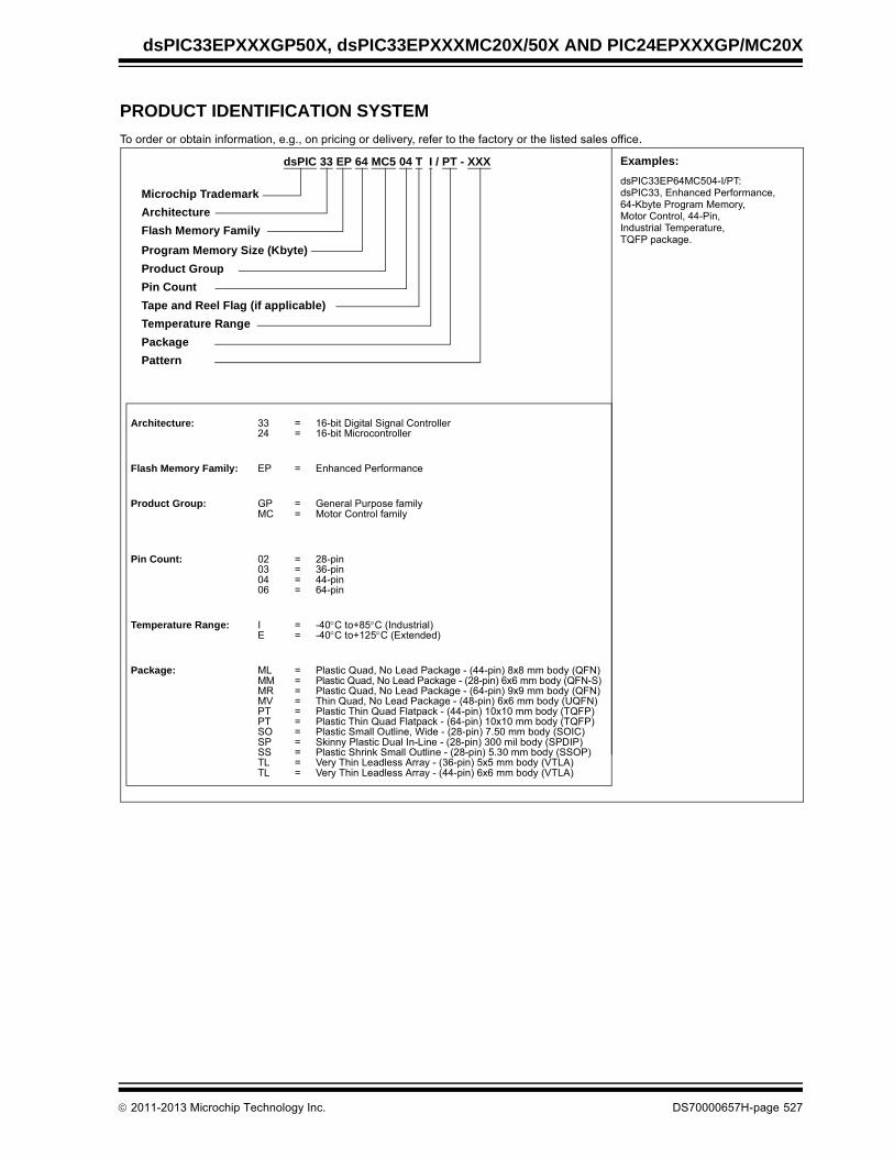
dsPIC33EPXXXGP50X, dsPIC33EPXXXMC20X/50X AND PIC24EPXXXGP/MC20X
PRODUCT IDENTIFICATION SYSTEM
To order or obtain information, e.g., on pricing or delivery, refer to the factory or the listed sales office.
Architecture: 33 = 16-bit Digital Signal Controller24 = 16-bit Microcontroller
Flash Memory Family: EP = Enhanced Performance
Product Group: GP = General Purpose familyMC = Motor Control family
Pin Count: 02 = 28-pin03 = 36-pin04 = 44-pin06 = 64-pin
Temperature Range: I = -40C to+85C (Industrial)E = -40C to+125C (Extended)
Package: ML = Plastic Quad, No Lead Package - (44-pin) 8x8 mm body (QFN)MM = Plastic Quad, No Lead Package - (28-pin) 6x6 mm body (QFN-S)MR = Plastic Quad, No Lead Package - (64-pin) 9x9 mm body (QFN)MV = Thin Quad, No Lead Package - (48-pin) 6x6 mm body (UQFN)PT = Plastic Thin Quad Flatpack - (44-pin) 10x10 mm body (TQFP)PT = Plastic Thin Quad Flatpack - (64-pin) 10x10 mm body (TQFP)SO = Plastic Small Outline, Wide - (28-pin) 7.50 mm body (SOIC)SP = Skinny Plastic Dual In-Line - (28-pin) 300 mil body (SPDIP)SS = Plastic Shrink Small Outline - (28-pin) 5.30 mm body (SSOP)TL = Very Thin Leadless Array - (36-pin) 5x5 mm body (VTLA)TL = Very Thin Leadless Array - (44-pin) 6x6 mm body (VTLA)
Examples:
dsPIC33EP64MC504-I/PT:dsPIC33, Enhanced Performance, 64-Kbyte Program Memory, Motor Control, 44-Pin, Industrial Temperature, TQFP package.
Microchip Trademark
Architecture
Flash Memory Family
Program Memory Size (Kbyte)
Product Group
Pin Count
Temperature Range
Package
Pattern
dsPIC 33 EP 64 MC5 04 T I / PT - XXX
Tape and Reel Flag (if applicable)
2011-2013 Microchip Technology Inc. DS70000657H-page 527

dsPIC33EPXXXGP50X, dsPIC33EPXXXMC20X/50X AND PIC24EPXXXGP/MC20X
NOTES:
DS70000657H-page 528 2011-2013 Microchip Technology Inc.

Note the following details of the code protection feature on Microchip devices:
• Microchip products meet the specification contained in their particular Microchip Data Sheet.
• Microchip believes that its family of products is one of the most secure families of its kind on the market today, when used in the intended manner and under normal conditions.
• There are dishonest and possibly illegal methods used to breach the code protection feature. All of these methods, to our knowledge, require using the Microchip products in a manner outside the operating specifications contained in Microchip’s Data Sheets. Most likely, the person doing so is engaged in theft of intellectual property.
• Microchip is willing to work with the customer who is concerned about the integrity of their code.
• Neither Microchip nor any other semiconductor manufacturer can guarantee the security of their code. Code protection does not mean that we are guaranteeing the product as “unbreakable.”
Code protection is constantly evolving. We at Microchip are committed to continuously improving the code protection features of ourproducts. Attempts to break Microchip’s code protection feature may be a violation of the Digital Millennium Copyright Act. If such actsallow unauthorized access to your software or other copyrighted work, you may have a right to sue for relief under that Act.
Information contained in this publication regarding deviceapplications and the like is provided only for your convenienceand may be superseded by updates. It is your responsibility toensure that your application meets with your specifications.MICROCHIP MAKES NO REPRESENTATIONS ORWARRANTIES OF ANY KIND WHETHER EXPRESS ORIMPLIED, WRITTEN OR ORAL, STATUTORY OROTHERWISE, RELATED TO THE INFORMATION,INCLUDING BUT NOT LIMITED TO ITS CONDITION,QUALITY, PERFORMANCE, MERCHANTABILITY ORFITNESS FOR PURPOSE. Microchip disclaims all liabilityarising from this information and its use. Use of Microchipdevices in life support and/or safety applications is entirely atthe buyer’s risk, and the buyer agrees to defend, indemnify andhold harmless Microchip from any and all damages, claims,suits, or expenses resulting from such use. No licenses areconveyed, implicitly or otherwise, under any Microchipintellectual property rights.
2011-2013 Microchip Technology Inc.
QUALITY MANAGEMENT SYSTEM CERTIFIED BY DNV
== ISO/TS 16949 ==
Trademarks
The Microchip name and logo, the Microchip logo, dsPIC, FlashFlex, KEELOQ, KEELOQ logo, MPLAB, PIC, PICmicro, PICSTART, PIC32 logo, rfPIC, SST, SST Logo, SuperFlash and UNI/O are registered trademarks of Microchip Technology Incorporated in the U.S.A. and other countries.
FilterLab, Hampshire, HI-TECH C, Linear Active Thermistor, MTP, SEEVAL and The Embedded Control Solutions Company are registered trademarks of Microchip Technology Incorporated in the U.S.A.
Silicon Storage Technology is a registered trademark of Microchip Technology Inc. in other countries.
Analog-for-the-Digital Age, Application Maestro, BodyCom, chipKIT, chipKIT logo, CodeGuard, dsPICDEM, dsPICDEM.net, dsPICworks, dsSPEAK, ECAN, ECONOMONITOR, FanSense, HI-TIDE, In-Circuit Serial Programming, ICSP, Mindi, MiWi, MPASM, MPF, MPLAB Certified logo, MPLIB, MPLINK, mTouch, Omniscient Code Generation, PICC, PICC-18, PICDEM, PICDEM.net, PICkit, PICtail, REAL ICE, rfLAB, Select Mode, SQI, Serial Quad I/O, Total Endurance, TSHARC, UniWinDriver, WiperLock, ZENA and Z-Scale are trademarks of Microchip Technology Incorporated in the U.S.A. and other countries.
SQTP is a service mark of Microchip Technology Incorporated in the U.S.A.
GestIC and ULPP are registered trademarks of Microchip Technology Germany II GmbH & Co. KG, a subsidiary of Microchip Technology Inc., in other countries.
All other trademarks mentioned herein are property of their respective companies.
© 2011-2013, Microchip Technology Incorporated, Printed in the U.S.A., All Rights Reserved.
Printed on recycled paper.
ISBN: 9781620773949
Microchip received ISO/TS-16949:2009 certification for its worldwide
DS70000657H-page 529
headquarters, design and wafer fabrication facilities in Chandler and Tempe, Arizona; Gresham, Oregon and design centers in California and India. The Company’s quality system processes and procedures are for its PIC® MCUs and dsPIC® DSCs, KEELOQ® code hopping devices, Serial EEPROMs, microperipherals, nonvolatile memory and analog products. In addition, Microchip’s quality system for the design and manufacture of development systems is ISO 9001:2000 certified.

DS70000657H-page 530 . 2011-2013 Microchip Technology Inc.
AMERICASCorporate Office2355 West Chandler Blvd.Chandler, AZ 85224-6199Tel: 480-792-7200 Fax: 480-792-7277Technical Support: http://www.microchip.com/supportWeb Address: www.microchip.com
AtlantaDuluth, GA Tel: 678-957-9614 Fax: 678-957-1455
BostonWestborough, MA Tel: 774-760-0087 Fax: 774-760-0088
ChicagoItasca, IL Tel: 630-285-0071 Fax: 630-285-0075
ClevelandIndependence, OH Tel: 216-447-0464 Fax: 216-447-0643
DallasAddison, TX Tel: 972-818-7423 Fax: 972-818-2924
DetroitFarmington Hills, MI Tel: 248-538-2250Fax: 248-538-2260
IndianapolisNoblesville, IN Tel: 317-773-8323Fax: 317-773-5453
Los AngelesMission Viejo, CA Tel: 949-462-9523 Fax: 949-462-9608
Santa ClaraSanta Clara, CA Tel: 408-961-6444Fax: 408-961-6445
TorontoMississauga, Ontario, CanadaTel: 905-673-0699 Fax: 905-673-6509
ASIA/PACIFICAsia Pacific OfficeSuites 3707-14, 37th FloorTower 6, The GatewayHarbour City, KowloonHong KongTel: 852-2401-1200Fax: 852-2401-3431
Australia - SydneyTel: 61-2-9868-6733Fax: 61-2-9868-6755
China - BeijingTel: 86-10-8569-7000 Fax: 86-10-8528-2104
China - ChengduTel: 86-28-8665-5511Fax: 86-28-8665-7889
China - ChongqingTel: 86-23-8980-9588Fax: 86-23-8980-9500
China - HangzhouTel: 86-571-2819-3187 Fax: 86-571-2819-3189
China - Hong Kong SARTel: 852-2943-5100 Fax: 852-2401-3431
China - NanjingTel: 86-25-8473-2460Fax: 86-25-8473-2470
China - QingdaoTel: 86-532-8502-7355Fax: 86-532-8502-7205
China - ShanghaiTel: 86-21-5407-5533 Fax: 86-21-5407-5066
China - ShenyangTel: 86-24-2334-2829Fax: 86-24-2334-2393
China - ShenzhenTel: 86-755-8864-2200 Fax: 86-755-8203-1760
China - WuhanTel: 86-27-5980-5300Fax: 86-27-5980-5118
China - XianTel: 86-29-8833-7252Fax: 86-29-8833-7256
China - XiamenTel: 86-592-2388138 Fax: 86-592-2388130
China - ZhuhaiTel: 86-756-3210040 Fax: 86-756-3210049
ASIA/PACIFICIndia - BangaloreTel: 91-80-3090-4444 Fax: 91-80-3090-4123
India - New DelhiTel: 91-11-4160-8631Fax: 91-11-4160-8632
India - PuneTel: 91-20-2566-1512Fax: 91-20-2566-1513
Japan - OsakaTel: 81-6-6152-7160 Fax: 81-6-6152-9310
Japan - TokyoTel: 81-3-6880- 3770 Fax: 81-3-6880-3771
Korea - DaeguTel: 82-53-744-4301Fax: 82-53-744-4302
Korea - SeoulTel: 82-2-554-7200Fax: 82-2-558-5932 or 82-2-558-5934
Malaysia - Kuala LumpurTel: 60-3-6201-9857Fax: 60-3-6201-9859
Malaysia - PenangTel: 60-4-227-8870Fax: 60-4-227-4068
Philippines - ManilaTel: 63-2-634-9065Fax: 63-2-634-9069
SingaporeTel: 65-6334-8870Fax: 65-6334-8850
Taiwan - Hsin ChuTel: 886-3-5778-366Fax: 886-3-5770-955
Taiwan - KaohsiungTel: 886-7-213-7828Fax: 886-7-330-9305
Taiwan - TaipeiTel: 886-2-2508-8600 Fax: 886-2-2508-0102
Thailand - BangkokTel: 66-2-694-1351Fax: 66-2-694-1350
EUROPEAustria - WelsTel: 43-7242-2244-39Fax: 43-7242-2244-393Denmark - CopenhagenTel: 45-4450-2828 Fax: 45-4485-2829
France - ParisTel: 33-1-69-53-63-20 Fax: 33-1-69-30-90-79
Germany - MunichTel: 49-89-627-144-0 Fax: 49-89-627-144-44
Italy - Milan Tel: 39-0331-742611 Fax: 39-0331-466781
Netherlands - DrunenTel: 31-416-690399 Fax: 31-416-690340
Spain - MadridTel: 34-91-708-08-90Fax: 34-91-708-08-91
UK - WokinghamTel: 44-118-921-5869Fax: 44-118-921-5820
Worldwide Sales and Service
11/29/12