Embed Size (px)
Citation preview

This is information on a product in full production.
September 2013 Doc ID 13453 Rev 4 1/186
1
ST10F273M
16-bit MCU with 512 Kbyte Flash memory and 36 Kbyte RAM
Datasheet − production data
Features
■ High performance 16-bit CPU with DSP functions– 50ns instruction cycle time at 40 MHz max
CPU clock– Multiply/accumulate unit (MAC) 16 x 16-bit
multiplication, 40-bit accumulator– Enhanced boolean bit manipulations– Single-cycle context switching support
■ Memory organization– 512 Kbyte on-chip Flash memory single
voltage with erase/program controller (full performance, 32-bit fetch)
– 100 K erasing/programming cycles– Up to 16 Mbyte linear address space for
code and data (5 Mbytes with CAN or I2C)– 2 Kbyte on-chip internal RAM (IRAM)– 34 Kbyte on-chip extension RAM (XRAM) – Programmable external bus configuration
and characteristics for different address ranges
– 5 programmable chip-select signals– Hold-acknowledge bus arbitration support
■ Interrupt– 8-channel peripheral event controller for
single cycle interrupt driven data transfer– 16-priority-level interrupt system with 56
sources, sampling rate down to 25ns
■ Timers– 2 multifunctional general purpose timer
units with 5 timers
■ Two 16-channel capture / compare units
■ 4-channel PWM unit + 4-channel XPWM
■ 24-channel A/D converter – 16-channel 10-bit, accuracy +/-2 LSB– 8-channel 10-bit, accuracy +/-5 LSB– 4.85µs Minimum conversion time
■ Serial channels– 2 synch. / asynch. serial channels– 2 high-speed synchronous channels– I2C standard interface
■ 2 CAN 2.0B interfaces operating on 1 or 2 CAN buses (64 or 2x32 messages, C-CAN version)
■ Fail-safe protection– Programmable watchdog timer– Oscillator watchdog
■ On-chip bootstrap loader
■ Clock generation– On-chip PLL and 4 to 12 MHz oscillator– Direct or prescaled clock input
■ Real time clock and 32 kHz on-chip oscillator
■ Up to 111 general purpose I/O lines– Individually programmable as input, output
or special function– Programmable threshold (hysteresis)
■ Idle, power down and standby modes
■ Single voltage supply: 5 V ±10% (embedded regulator for 1.8 V core supply)
■ Temperature range: -40°C to 125°C
PQFP144 (28 x 28 x 3.4mm)(Plastic Quad Flat Package)
LQFP144 (20 x 20 x 1.4mm)(Low Profile Quad Flat Package)
www.st.com

Contents ST10F273M
2/186 Doc ID 13453 Rev 4
Contents
1 Introduction . . . . . . . . . . . . . . . . . . . . . . . . . . . . . . . . . . . . . . . . . . . . . . . 11
1.1 Description . . . . . . . . . . . . . . . . . . . . . . . . . . . . . . . . . . . . . . . . . . . . . . . . 11
1.2 Special characteristics . . . . . . . . . . . . . . . . . . . . . . . . . . . . . . . . . . . . . . . 11
1.2.1 X-Peripheral clock gating . . . . . . . . . . . . . . . . . . . . . . . . . . . . . . . . . . . . 11
1.2.2 Improved supply ring . . . . . . . . . . . . . . . . . . . . . . . . . . . . . . . . . . . . . . . 11
2 Pin data . . . . . . . . . . . . . . . . . . . . . . . . . . . . . . . . . . . . . . . . . . . . . . . . . . 13
3 Functional description . . . . . . . . . . . . . . . . . . . . . . . . . . . . . . . . . . . . . . 20
4 Memory organization . . . . . . . . . . . . . . . . . . . . . . . . . . . . . . . . . . . . . . . 21
5 Internal Flash memory . . . . . . . . . . . . . . . . . . . . . . . . . . . . . . . . . . . . . . 27
5.1 Overview . . . . . . . . . . . . . . . . . . . . . . . . . . . . . . . . . . . . . . . . . . . . . . . . . 27
5.2 Functional description . . . . . . . . . . . . . . . . . . . . . . . . . . . . . . . . . . . . . . . 27
5.2.1 Structure . . . . . . . . . . . . . . . . . . . . . . . . . . . . . . . . . . . . . . . . . . . . . . . . 27
5.2.2 Module structure . . . . . . . . . . . . . . . . . . . . . . . . . . . . . . . . . . . . . . . . . . 27
5.2.3 Low power mode . . . . . . . . . . . . . . . . . . . . . . . . . . . . . . . . . . . . . . . . . . 30
5.3 Write operation . . . . . . . . . . . . . . . . . . . . . . . . . . . . . . . . . . . . . . . . . . . . . 30
5.4 Flash control registers description . . . . . . . . . . . . . . . . . . . . . . . . . . . . . . 31
5.4.1 Flash control register 0 low (FCR0L) . . . . . . . . . . . . . . . . . . . . . . . . . . . 31
5.4.2 Flash control register 0 high (FCR0H) . . . . . . . . . . . . . . . . . . . . . . . . . . 33
5.4.3 Flash control register 1 low (FCR1L) . . . . . . . . . . . . . . . . . . . . . . . . . . . 35
5.4.4 Flash control register 1 high (FCR1H) . . . . . . . . . . . . . . . . . . . . . . . . . . 36
5.4.5 Flash data register 0 low (FDR0L) . . . . . . . . . . . . . . . . . . . . . . . . . . . . . 37
5.4.6 Flash data register 0 high (FDR0H) . . . . . . . . . . . . . . . . . . . . . . . . . . . . 37
5.4.7 Flash data register 1 low (FDR1L) . . . . . . . . . . . . . . . . . . . . . . . . . . . . . 38
5.4.8 Flash data register 1 high (FDR1H) . . . . . . . . . . . . . . . . . . . . . . . . . . . . 38
5.4.9 Flash address register low (FARL) . . . . . . . . . . . . . . . . . . . . . . . . . . . . . 38
5.4.10 Flash address register high (FARH) . . . . . . . . . . . . . . . . . . . . . . . . . . . . 39
5.4.11 Flash error register (FER) . . . . . . . . . . . . . . . . . . . . . . . . . . . . . . . . . . . 39
5.4.12 XFlash interface control dummy register (XFICR) . . . . . . . . . . . . . . . . . 40
5.5 Protection strategy . . . . . . . . . . . . . . . . . . . . . . . . . . . . . . . . . . . . . . . . . . 40
5.5.1 Protection registers . . . . . . . . . . . . . . . . . . . . . . . . . . . . . . . . . . . . . . . . 41
ST10F273M Contents
Doc ID 13453 Rev 4 3/186
5.5.2 Flash non-volatile write protection I register low (FNVWPIRL) . . . . . . . 41
5.5.3 Flash non-volatile write protection I register high (FNVWPIRH) . . . . . . 42
5.5.4 Flash non-volatile write protection I register low Mirror (FNVWPIRL-m) 42
5.5.5 Flash non-volatile write protection I register high Mirror (FVWPIRH-m) 42
5.5.6 Flash non-volatile access protection register 0 (FNVAPR0) . . . . . . . . . 43
5.5.7 Flash non-volatile access protection register 1 low (FNVAPR1L) . . . . . 43
5.5.8 Flash non-volatile access protection register 1 high (FNVAPR1H) . . . . 44
5.5.9 Access protection . . . . . . . . . . . . . . . . . . . . . . . . . . . . . . . . . . . . . . . . . 44
5.5.10 Write protection . . . . . . . . . . . . . . . . . . . . . . . . . . . . . . . . . . . . . . . . . . . 45
5.5.11 Temporary unprotection . . . . . . . . . . . . . . . . . . . . . . . . . . . . . . . . . . . . . 45
5.6 Write operation examples . . . . . . . . . . . . . . . . . . . . . . . . . . . . . . . . . . . . . 45
5.7 Write operation summary . . . . . . . . . . . . . . . . . . . . . . . . . . . . . . . . . . . . . 48
6 Bootstrap loader . . . . . . . . . . . . . . . . . . . . . . . . . . . . . . . . . . . . . . . . . . . 49
6.1 Selection among user-code, standard or selective bootstrap . . . . . . . . . . 49
6.2 Standard bootstrap loader . . . . . . . . . . . . . . . . . . . . . . . . . . . . . . . . . . . . 49
6.3 Alternate and selective boot mode (ABM and SBM) . . . . . . . . . . . . . . . . 50
6.3.1 Activation of the ABM and SBM . . . . . . . . . . . . . . . . . . . . . . . . . . . . . . . 50
6.3.2 User mode signature integrity check . . . . . . . . . . . . . . . . . . . . . . . . . . . 50
6.3.3 Selective boot mode . . . . . . . . . . . . . . . . . . . . . . . . . . . . . . . . . . . . . . . 50
7 Central processing unit (CPU) . . . . . . . . . . . . . . . . . . . . . . . . . . . . . . . . 51
7.1 Multiplier-accumulator unit (MAC) . . . . . . . . . . . . . . . . . . . . . . . . . . . . . . 52
7.2 Instruction set summary . . . . . . . . . . . . . . . . . . . . . . . . . . . . . . . . . . . . . . 53
7.3 MAC co-processor specific instructions . . . . . . . . . . . . . . . . . . . . . . . . . . 55
8 External bus controller . . . . . . . . . . . . . . . . . . . . . . . . . . . . . . . . . . . . . . 56
9 Interrupt system . . . . . . . . . . . . . . . . . . . . . . . . . . . . . . . . . . . . . . . . . . . 57
9.1 X-Peripheral interrupt . . . . . . . . . . . . . . . . . . . . . . . . . . . . . . . . . . . . . . . . 59
9.2 Exception and error traps list . . . . . . . . . . . . . . . . . . . . . . . . . . . . . . . . . . 61
10 Capture / compare (CAPCOM) units . . . . . . . . . . . . . . . . . . . . . . . . . . . 62
11 General purpose timer unit . . . . . . . . . . . . . . . . . . . . . . . . . . . . . . . . . . 64
11.1 GPT1 . . . . . . . . . . . . . . . . . . . . . . . . . . . . . . . . . . . . . . . . . . . . . . . . . . . . 64
Contents ST10F273M
4/186 Doc ID 13453 Rev 4
11.2 GPT2 . . . . . . . . . . . . . . . . . . . . . . . . . . . . . . . . . . . . . . . . . . . . . . . . . . . . 66
12 PWM modules . . . . . . . . . . . . . . . . . . . . . . . . . . . . . . . . . . . . . . . . . . . . . 68
13 Parallel ports . . . . . . . . . . . . . . . . . . . . . . . . . . . . . . . . . . . . . . . . . . . . . . 69
13.1 Introduction . . . . . . . . . . . . . . . . . . . . . . . . . . . . . . . . . . . . . . . . . . . . . . . 69
13.2 I/O’s special features . . . . . . . . . . . . . . . . . . . . . . . . . . . . . . . . . . . . . . . . 69
13.2.1 Open drain mode . . . . . . . . . . . . . . . . . . . . . . . . . . . . . . . . . . . . . . . . . . 69
13.2.2 Input threshold control . . . . . . . . . . . . . . . . . . . . . . . . . . . . . . . . . . . . . . 70
13.3 Alternate port functions . . . . . . . . . . . . . . . . . . . . . . . . . . . . . . . . . . . . . . 70
14 A/D converter . . . . . . . . . . . . . . . . . . . . . . . . . . . . . . . . . . . . . . . . . . . . . . 72
15 Serial channels . . . . . . . . . . . . . . . . . . . . . . . . . . . . . . . . . . . . . . . . . . . . 74
15.1 Asynchronous / synchronous serial interfaces . . . . . . . . . . . . . . . . . . . . . 74
15.2 ASCx in asynchronous mode . . . . . . . . . . . . . . . . . . . . . . . . . . . . . . . . . . 74
15.3 ASCx in synchronous mode . . . . . . . . . . . . . . . . . . . . . . . . . . . . . . . . . . . 75
15.4 High speed synchronous serial interfaces . . . . . . . . . . . . . . . . . . . . . . . . 75
16 I2C interface . . . . . . . . . . . . . . . . . . . . . . . . . . . . . . . . . . . . . . . . . . . . . . . 77
17 CAN modules . . . . . . . . . . . . . . . . . . . . . . . . . . . . . . . . . . . . . . . . . . . . . . 78
17.1 Configuration support . . . . . . . . . . . . . . . . . . . . . . . . . . . . . . . . . . . . . . . . 78
17.2 CAN bus configurations . . . . . . . . . . . . . . . . . . . . . . . . . . . . . . . . . . . . . . 78
17.2.1 Single CAN bus . . . . . . . . . . . . . . . . . . . . . . . . . . . . . . . . . . . . . . . . . . . 79
17.2.2 Multiple CAN bus . . . . . . . . . . . . . . . . . . . . . . . . . . . . . . . . . . . . . . . . . . 80
17.2.3 Parallel mode . . . . . . . . . . . . . . . . . . . . . . . . . . . . . . . . . . . . . . . . . . . . . 80
18 Real time clock . . . . . . . . . . . . . . . . . . . . . . . . . . . . . . . . . . . . . . . . . . . . 81
19 Watchdog timer . . . . . . . . . . . . . . . . . . . . . . . . . . . . . . . . . . . . . . . . . . . . 82
20 System reset . . . . . . . . . . . . . . . . . . . . . . . . . . . . . . . . . . . . . . . . . . . . . . 83
20.1 Input filter . . . . . . . . . . . . . . . . . . . . . . . . . . . . . . . . . . . . . . . . . . . . . . . . . 83
20.2 Asynchronous reset . . . . . . . . . . . . . . . . . . . . . . . . . . . . . . . . . . . . . . . . . 84
20.3 Synchronous reset (warm reset) . . . . . . . . . . . . . . . . . . . . . . . . . . . . . . . 89
ST10F273M Contents
Doc ID 13453 Rev 4 5/186
20.4 Software reset . . . . . . . . . . . . . . . . . . . . . . . . . . . . . . . . . . . . . . . . . . . . . 95
20.5 Watchdog timer reset . . . . . . . . . . . . . . . . . . . . . . . . . . . . . . . . . . . . . . . . 96
20.6 Bidirectional reset . . . . . . . . . . . . . . . . . . . . . . . . . . . . . . . . . . . . . . . . . . . 97
20.7 Reset circuitry . . . . . . . . . . . . . . . . . . . . . . . . . . . . . . . . . . . . . . . . . . . . 101
20.8 Reset application examples . . . . . . . . . . . . . . . . . . . . . . . . . . . . . . . . . . 104
20.9 Reset summary . . . . . . . . . . . . . . . . . . . . . . . . . . . . . . . . . . . . . . . . . . . 106
21 Power reduction modes . . . . . . . . . . . . . . . . . . . . . . . . . . . . . . . . . . . . 109
21.1 Idle mode . . . . . . . . . . . . . . . . . . . . . . . . . . . . . . . . . . . . . . . . . . . . . . . . 109
21.2 Power-down mode . . . . . . . . . . . . . . . . . . . . . . . . . . . . . . . . . . . . . . . . . 109
21.2.1 Protected power-down mode . . . . . . . . . . . . . . . . . . . . . . . . . . . . . . . . 110
21.2.2 Interruptible power-down mode . . . . . . . . . . . . . . . . . . . . . . . . . . . . . . 110
21.3 Standby mode . . . . . . . . . . . . . . . . . . . . . . . . . . . . . . . . . . . . . . . . . . . . 110
21.3.1 Entering standby mode . . . . . . . . . . . . . . . . . . . . . . . . . . . . . . . . . . . . 111
21.3.2 Exiting standby mode . . . . . . . . . . . . . . . . . . . . . . . . . . . . . . . . . . . . . 112
21.3.3 Real time clock and standby mode . . . . . . . . . . . . . . . . . . . . . . . . . . . 112
21.3.4 Power reduction modes summary . . . . . . . . . . . . . . . . . . . . . . . . . . . . 112
22 Programmable output clock divider . . . . . . . . . . . . . . . . . . . . . . . . . . 114
23 Register set . . . . . . . . . . . . . . . . . . . . . . . . . . . . . . . . . . . . . . . . . . . . . . 115
23.1 Special function registers . . . . . . . . . . . . . . . . . . . . . . . . . . . . . . . . . . . . 115
23.2 X-registers . . . . . . . . . . . . . . . . . . . . . . . . . . . . . . . . . . . . . . . . . . . . . . . 123
23.3 Flash registers ordered by name . . . . . . . . . . . . . . . . . . . . . . . . . . . . . . 128
23.4 Identification registers . . . . . . . . . . . . . . . . . . . . . . . . . . . . . . . . . . . . . . 128
24 Electrical characteristics . . . . . . . . . . . . . . . . . . . . . . . . . . . . . . . . . . . 131
24.1 Absolute maximum ratings . . . . . . . . . . . . . . . . . . . . . . . . . . . . . . . . . . . 131
24.2 Recommended operating conditions . . . . . . . . . . . . . . . . . . . . . . . . . . . 132
24.3 Power considerations . . . . . . . . . . . . . . . . . . . . . . . . . . . . . . . . . . . . . . . 132
24.4 Parameter interpretation . . . . . . . . . . . . . . . . . . . . . . . . . . . . . . . . . . . . . 133
24.5 DC characteristics . . . . . . . . . . . . . . . . . . . . . . . . . . . . . . . . . . . . . . . . . 134
24.6 Flash characteristics . . . . . . . . . . . . . . . . . . . . . . . . . . . . . . . . . . . . . . . 138
24.7 A/D converter characteristics . . . . . . . . . . . . . . . . . . . . . . . . . . . . . . . . . 139
24.7.1 Conversion timing control . . . . . . . . . . . . . . . . . . . . . . . . . . . . . . . . . . 140

Contents ST10F273M
6/186 Doc ID 13453 Rev 4
24.7.2 A/D conversion accuracy . . . . . . . . . . . . . . . . . . . . . . . . . . . . . . . . . . . 141
24.7.3 Total unadjusted error . . . . . . . . . . . . . . . . . . . . . . . . . . . . . . . . . . . . . 142
24.7.4 Analog reference pins . . . . . . . . . . . . . . . . . . . . . . . . . . . . . . . . . . . . . 143
24.8 AC characteristics . . . . . . . . . . . . . . . . . . . . . . . . . . . . . . . . . . . . . . . . . 149
24.8.1 Test waveforms . . . . . . . . . . . . . . . . . . . . . . . . . . . . . . . . . . . . . . . . . . 149
24.8.2 Definition of internal timing . . . . . . . . . . . . . . . . . . . . . . . . . . . . . . . . . 150
24.8.3 Clock generation modes . . . . . . . . . . . . . . . . . . . . . . . . . . . . . . . . . . . 151
24.8.4 Prescaler operation . . . . . . . . . . . . . . . . . . . . . . . . . . . . . . . . . . . . . . . 151
24.8.5 Direct drive . . . . . . . . . . . . . . . . . . . . . . . . . . . . . . . . . . . . . . . . . . . . . . 151
24.8.6 Oscillator watchdog (OWD) . . . . . . . . . . . . . . . . . . . . . . . . . . . . . . . . . 152
24.8.7 Phase locked loop (PLL) . . . . . . . . . . . . . . . . . . . . . . . . . . . . . . . . . . . 152
24.8.8 Voltage controlled oscillator . . . . . . . . . . . . . . . . . . . . . . . . . . . . . . . . . 153
24.8.9 PLL jitter . . . . . . . . . . . . . . . . . . . . . . . . . . . . . . . . . . . . . . . . . . . . . . . . 154
24.8.10 PLL lock / unlock . . . . . . . . . . . . . . . . . . . . . . . . . . . . . . . . . . . . . . . . . 156
24.8.11 Main oscillator specifications . . . . . . . . . . . . . . . . . . . . . . . . . . . . . . . . 157
24.8.12 32 kHz oscillator specifications . . . . . . . . . . . . . . . . . . . . . . . . . . . . . . 158
24.8.13 External clock drive XTAL1 . . . . . . . . . . . . . . . . . . . . . . . . . . . . . . . . . 159
24.8.14 Memory cycle variables . . . . . . . . . . . . . . . . . . . . . . . . . . . . . . . . . . . . 160
24.8.15 External memory bus timing . . . . . . . . . . . . . . . . . . . . . . . . . . . . . . . . 160
24.8.16 Multiplexed bus . . . . . . . . . . . . . . . . . . . . . . . . . . . . . . . . . . . . . . . . . . 160
24.8.17 Demultiplexed bus . . . . . . . . . . . . . . . . . . . . . . . . . . . . . . . . . . . . . . . . 167
24.8.18 CLKOUT and READY . . . . . . . . . . . . . . . . . . . . . . . . . . . . . . . . . . . . . 173
24.8.19 External bus arbitration . . . . . . . . . . . . . . . . . . . . . . . . . . . . . . . . . . . . 174
24.8.20 High-speed synchronous serial interface (SSC) timing . . . . . . . . . . . . 177
25 Package information . . . . . . . . . . . . . . . . . . . . . . . . . . . . . . . . . . . . . . . 180
25.1 ECOPACK® . . . . . . . . . . . . . . . . . . . . . . . . . . . . . . . . . . . . . . . . . . . . . . 180
25.2 PQFP144 mechanical data . . . . . . . . . . . . . . . . . . . . . . . . . . . . . . . . . . 180
25.3 LQFP144 mechanical data . . . . . . . . . . . . . . . . . . . . . . . . . . . . . . . . . . . 182
26 Ordering information . . . . . . . . . . . . . . . . . . . . . . . . . . . . . . . . . . . . . . 184
27 Revision history . . . . . . . . . . . . . . . . . . . . . . . . . . . . . . . . . . . . . . . . . . 185

ST10F273M List of tables
Doc ID 13453 Rev 4 7/186
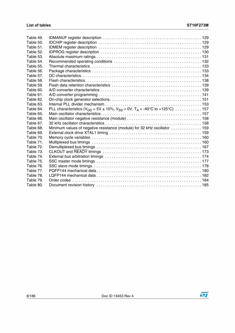
List of tables
Table 1. Pin description . . . . . . . . . . . . . . . . . . . . . . . . . . . . . . . . . . . . . . . . . . . . . . . . . . . . . . . . . . 14Table 2. Summary of IFlash address range . . . . . . . . . . . . . . . . . . . . . . . . . . . . . . . . . . . . . . . . . . . 21Table 3. Flash module address space . . . . . . . . . . . . . . . . . . . . . . . . . . . . . . . . . . . . . . . . . . . . . . . 27Table 4. Flash module sectorization (read operations). . . . . . . . . . . . . . . . . . . . . . . . . . . . . . . . . . . 28Table 5. Flash module sectorization (write operations, or ROMS1 = ‘1’) . . . . . . . . . . . . . . . . . . . . . 29Table 6. Flash control registers summary. . . . . . . . . . . . . . . . . . . . . . . . . . . . . . . . . . . . . . . . . . . . . 30Table 7. FCR0L register description . . . . . . . . . . . . . . . . . . . . . . . . . . . . . . . . . . . . . . . . . . . . . . . . . 31Table 8. FCR0H register description . . . . . . . . . . . . . . . . . . . . . . . . . . . . . . . . . . . . . . . . . . . . . . . . 33Table 9. FCR1L register description . . . . . . . . . . . . . . . . . . . . . . . . . . . . . . . . . . . . . . . . . . . . . . . . . 35Table 10. FCR1H register description . . . . . . . . . . . . . . . . . . . . . . . . . . . . . . . . . . . . . . . . . . . . . . . . 36Table 11. Bank (BxS) and sectors (BxFy) status bits meaning. . . . . . . . . . . . . . . . . . . . . . . . . . . . . . 36Table 12. FDR0L register description . . . . . . . . . . . . . . . . . . . . . . . . . . . . . . . . . . . . . . . . . . . . . . . . . 37Table 13. FDR0H register description . . . . . . . . . . . . . . . . . . . . . . . . . . . . . . . . . . . . . . . . . . . . . . . . 37Table 14. FDR1L register description . . . . . . . . . . . . . . . . . . . . . . . . . . . . . . . . . . . . . . . . . . . . . . . . . 38Table 15. FDR1H register description . . . . . . . . . . . . . . . . . . . . . . . . . . . . . . . . . . . . . . . . . . . . . . . . 38Table 16. FARL register description . . . . . . . . . . . . . . . . . . . . . . . . . . . . . . . . . . . . . . . . . . . . . . . . . . 38Table 17. FARH register description. . . . . . . . . . . . . . . . . . . . . . . . . . . . . . . . . . . . . . . . . . . . . . . . . . 39Table 18. FER register bits . . . . . . . . . . . . . . . . . . . . . . . . . . . . . . . . . . . . . . . . . . . . . . . . . . . . . . . . . 39Table 19. XFlash interface control register . . . . . . . . . . . . . . . . . . . . . . . . . . . . . . . . . . . . . . . . . . . . . 40Table 20. FNVWPIRL register bits . . . . . . . . . . . . . . . . . . . . . . . . . . . . . . . . . . . . . . . . . . . . . . . . . . . 41Table 21. FNVWPRIH register bits . . . . . . . . . . . . . . . . . . . . . . . . . . . . . . . . . . . . . . . . . . . . . . . . . . . 42Table 22. FNVAPR0 register bits . . . . . . . . . . . . . . . . . . . . . . . . . . . . . . . . . . . . . . . . . . . . . . . . . . . . 43Table 23. FNVAPR1L register bits . . . . . . . . . . . . . . . . . . . . . . . . . . . . . . . . . . . . . . . . . . . . . . . . . . . 43Table 24. FNVAPR1H register bits . . . . . . . . . . . . . . . . . . . . . . . . . . . . . . . . . . . . . . . . . . . . . . . . . . 44Table 25. Summary of access protection level . . . . . . . . . . . . . . . . . . . . . . . . . . . . . . . . . . . . . . . . . . 44Table 26. Flash write operations. . . . . . . . . . . . . . . . . . . . . . . . . . . . . . . . . . . . . . . . . . . . . . . . . . . . . 48Table 27. ST10F273M boot mode selection. . . . . . . . . . . . . . . . . . . . . . . . . . . . . . . . . . . . . . . . . . . . 49Table 28. Standard instruction set summary . . . . . . . . . . . . . . . . . . . . . . . . . . . . . . . . . . . . . . . . . . . 53Table 29. MAC instruction set summary. . . . . . . . . . . . . . . . . . . . . . . . . . . . . . . . . . . . . . . . . . . . . . . 55Table 30. Interrupt sources. . . . . . . . . . . . . . . . . . . . . . . . . . . . . . . . . . . . . . . . . . . . . . . . . . . . . . . . . 57Table 31. X-Interrupt detailed mapping . . . . . . . . . . . . . . . . . . . . . . . . . . . . . . . . . . . . . . . . . . . . . . . 60Table 32. Trap priorities . . . . . . . . . . . . . . . . . . . . . . . . . . . . . . . . . . . . . . . . . . . . . . . . . . . . . . . . . . . 61Table 33. Compare modes . . . . . . . . . . . . . . . . . . . . . . . . . . . . . . . . . . . . . . . . . . . . . . . . . . . . . . . . . 62Table 34. CAPCOM timer input frequencies, resolutions and periods at 40 MHz . . . . . . . . . . . . . . . 63Table 35. GPT1 timer input frequencies, resolutions and periods at 40 MHz. . . . . . . . . . . . . . . . . . . 64Table 36. GPT2 timer input frequencies, resolutions and periods at 40 MHz. . . . . . . . . . . . . . . . . . . 66Table 37. PWM unit frequencies and resolutions at 40 MHz CPU clock . . . . . . . . . . . . . . . . . . . . . . 68Table 38. ASC asynchronous baudrates by reload value and deviation errors . . . . . . . . . . . . . . . . . 74Table 39. ASC synchronous baudrates by reload value and deviation errors . . . . . . . . . . . . . . . . . . 75Table 40. SSC synchronous baudrate and reload values . . . . . . . . . . . . . . . . . . . . . . . . . . . . . . . . . 76Table 41. WDTREL reload value . . . . . . . . . . . . . . . . . . . . . . . . . . . . . . . . . . . . . . . . . . . . . . . . . . . . 82Table 42. Reset event definition . . . . . . . . . . . . . . . . . . . . . . . . . . . . . . . . . . . . . . . . . . . . . . . . . . . . . 83Table 43. Reset event. . . . . . . . . . . . . . . . . . . . . . . . . . . . . . . . . . . . . . . . . . . . . . . . . . . . . . . . . . . . 106Table 44. PORT0 latched configuration for the different reset events . . . . . . . . . . . . . . . . . . . . . . . 107Table 45. Power reduction modes summary . . . . . . . . . . . . . . . . . . . . . . . . . . . . . . . . . . . . . . . . . . 113Table 46. List of special function registers . . . . . . . . . . . . . . . . . . . . . . . . . . . . . . . . . . . . . . . . . . . . 115Table 47. List of XBus registers . . . . . . . . . . . . . . . . . . . . . . . . . . . . . . . . . . . . . . . . . . . . . . . . . . . . 123Table 48. List of Flash control registers . . . . . . . . . . . . . . . . . . . . . . . . . . . . . . . . . . . . . . . . . . . . . . 128
List of tables ST10F273M
8/186 Doc ID 13453 Rev 4
Table 49. IDMANUF register description . . . . . . . . . . . . . . . . . . . . . . . . . . . . . . . . . . . . . . . . . . . . . 129Table 50. IDCHIP register description . . . . . . . . . . . . . . . . . . . . . . . . . . . . . . . . . . . . . . . . . . . . . . . 129Table 51. IDMEM register description . . . . . . . . . . . . . . . . . . . . . . . . . . . . . . . . . . . . . . . . . . . . . . . 129Table 52. IDPROG register description . . . . . . . . . . . . . . . . . . . . . . . . . . . . . . . . . . . . . . . . . . . . . . 130Table 53. Absolute maximum ratings . . . . . . . . . . . . . . . . . . . . . . . . . . . . . . . . . . . . . . . . . . . . . . . . 131Table 54. Recommended operating conditions . . . . . . . . . . . . . . . . . . . . . . . . . . . . . . . . . . . . . . . . 132Table 55. Thermal characteristics. . . . . . . . . . . . . . . . . . . . . . . . . . . . . . . . . . . . . . . . . . . . . . . . . . . 133Table 56. Package characteristics . . . . . . . . . . . . . . . . . . . . . . . . . . . . . . . . . . . . . . . . . . . . . . . . . . 133Table 57. DC characteristics. . . . . . . . . . . . . . . . . . . . . . . . . . . . . . . . . . . . . . . . . . . . . . . . . . . . . . . 134Table 58. Flash characteristics . . . . . . . . . . . . . . . . . . . . . . . . . . . . . . . . . . . . . . . . . . . . . . . . . . . . . 138Table 59. Flash data retention characteristics . . . . . . . . . . . . . . . . . . . . . . . . . . . . . . . . . . . . . . . . . 139Table 60. A/D converter characteristics . . . . . . . . . . . . . . . . . . . . . . . . . . . . . . . . . . . . . . . . . . . . . . 139Table 61. A/D converter programming . . . . . . . . . . . . . . . . . . . . . . . . . . . . . . . . . . . . . . . . . . . . . . . 141Table 62. On-chip clock generator selections. . . . . . . . . . . . . . . . . . . . . . . . . . . . . . . . . . . . . . . . . . 151Table 63. Internal PLL divider mechanism . . . . . . . . . . . . . . . . . . . . . . . . . . . . . . . . . . . . . . . . . . . . 153Table 64. PLL characteristics (VDD = 5V ± 10%, VSS = 0V, TA = -40°C to +125°C) . . . . . . . . . . . . 157Table 65. Main oscillator characteristics . . . . . . . . . . . . . . . . . . . . . . . . . . . . . . . . . . . . . . . . . . . . . . 157Table 66. Main oscillator negative resistance (module) . . . . . . . . . . . . . . . . . . . . . . . . . . . . . . . . . . 158Table 67. 32 kHz oscillator characteristics . . . . . . . . . . . . . . . . . . . . . . . . . . . . . . . . . . . . . . . . . . . . 158Table 68. Minimum values of negative resistance (module) for 32 kHz oscillator . . . . . . . . . . . . . . 159Table 69. External clock drive XTAL1 timing . . . . . . . . . . . . . . . . . . . . . . . . . . . . . . . . . . . . . . . . . . 159Table 70. Memory cycle variables . . . . . . . . . . . . . . . . . . . . . . . . . . . . . . . . . . . . . . . . . . . . . . . . . . 160Table 71. Multiplexed bus timings . . . . . . . . . . . . . . . . . . . . . . . . . . . . . . . . . . . . . . . . . . . . . . . . . . 160Table 72. Demultiplexed bus timings . . . . . . . . . . . . . . . . . . . . . . . . . . . . . . . . . . . . . . . . . . . . . . . . 167Table 73. CLKOUT and READY timings . . . . . . . . . . . . . . . . . . . . . . . . . . . . . . . . . . . . . . . . . . . . . 173Table 74. External bus arbitration timings . . . . . . . . . . . . . . . . . . . . . . . . . . . . . . . . . . . . . . . . . . . . 174Table 75. SSC master mode timings . . . . . . . . . . . . . . . . . . . . . . . . . . . . . . . . . . . . . . . . . . . . . . . . 177Table 76. SSC slave mode timings. . . . . . . . . . . . . . . . . . . . . . . . . . . . . . . . . . . . . . . . . . . . . . . . . . 178Table 77. PQFP144 mechanical data. . . . . . . . . . . . . . . . . . . . . . . . . . . . . . . . . . . . . . . . . . . . . . . . 180Table 78. LQFP144 mechanical data . . . . . . . . . . . . . . . . . . . . . . . . . . . . . . . . . . . . . . . . . . . . . . . . 182Table 79. Order codes . . . . . . . . . . . . . . . . . . . . . . . . . . . . . . . . . . . . . . . . . . . . . . . . . . . . . . . . . . . 184Table 80. Document revision history . . . . . . . . . . . . . . . . . . . . . . . . . . . . . . . . . . . . . . . . . . . . . . . . 185

ST10F273M List of figures
Doc ID 13453 Rev 4 9/186
List of figures
Figure 1. ST10F273M logic symbol . . . . . . . . . . . . . . . . . . . . . . . . . . . . . . . . . . . . . . . . . . . . . . . . . . 12Figure 2. Pin configuration (top view) . . . . . . . . . . . . . . . . . . . . . . . . . . . . . . . . . . . . . . . . . . . . . . . . 13Figure 3. Block diagram . . . . . . . . . . . . . . . . . . . . . . . . . . . . . . . . . . . . . . . . . . . . . . . . . . . . . . . . . . . 20Figure 4. ST10F273M memory mapping (XADRS3 = 800Bh - reset value) . . . . . . . . . . . . . . . . . . . 25Figure 5. ST10F273M memory mapping (XADRS3 = E009h - user programmed value) . . . . . . . . . 26Figure 6. Flash structure . . . . . . . . . . . . . . . . . . . . . . . . . . . . . . . . . . . . . . . . . . . . . . . . . . . . . . . . . . 27Figure 7. Write operation control flow . . . . . . . . . . . . . . . . . . . . . . . . . . . . . . . . . . . . . . . . . . . . . . . . 48Figure 8. CPU block diagram (MAC unit not included) . . . . . . . . . . . . . . . . . . . . . . . . . . . . . . . . . . . 51Figure 9. MAC unit architecture . . . . . . . . . . . . . . . . . . . . . . . . . . . . . . . . . . . . . . . . . . . . . . . . . . . . . 52Figure 10. X-Interrupt basic structure . . . . . . . . . . . . . . . . . . . . . . . . . . . . . . . . . . . . . . . . . . . . . . . . . 60Figure 11. Block diagram of GPT1. . . . . . . . . . . . . . . . . . . . . . . . . . . . . . . . . . . . . . . . . . . . . . . . . . . . 65Figure 12. Block diagram of GPT2. . . . . . . . . . . . . . . . . . . . . . . . . . . . . . . . . . . . . . . . . . . . . . . . . . . . 67Figure 13. Block diagram of PWM module . . . . . . . . . . . . . . . . . . . . . . . . . . . . . . . . . . . . . . . . . . . . . 68Figure 14. Connection to single CAN bus via separate CAN transceivers . . . . . . . . . . . . . . . . . . . . . 79Figure 15. Connection to single CAN bus via common CAN transceivers. . . . . . . . . . . . . . . . . . . . . . 79Figure 16. Connection to two different CAN buses (for example for gateway application) . . . . . . . . . 80Figure 17. Connection to one CAN bus with internal parallel mode enabled. . . . . . . . . . . . . . . . . . . . 80Figure 18. Asynchronous power-on RESET (EA = 1) . . . . . . . . . . . . . . . . . . . . . . . . . . . . . . . . . . . . . 86Figure 19. Asynchronous power-on RESET (EA = 0) . . . . . . . . . . . . . . . . . . . . . . . . . . . . . . . . . . . . . 87Figure 20. Asynchronous hardware RESET (EA = 1) . . . . . . . . . . . . . . . . . . . . . . . . . . . . . . . . . . . . . 88Figure 21. Asynchronous hardware RESET (EA = 0) . . . . . . . . . . . . . . . . . . . . . . . . . . . . . . . . . . . . . 89Figure 22. Synchronous short / long hardware RESET (EA = 1). . . . . . . . . . . . . . . . . . . . . . . . . . . . . 92Figure 23. Synchronous short / long hardware RESET (EA = 0). . . . . . . . . . . . . . . . . . . . . . . . . . . . . 93Figure 24. Synchronous long hardware RESET (EA = 1) . . . . . . . . . . . . . . . . . . . . . . . . . . . . . . . . . . 94Figure 25. Synchronous long hardware RESET (EA = 0) . . . . . . . . . . . . . . . . . . . . . . . . . . . . . . . . . . 95Figure 26. SW / WDT unidirectional RESET (EA = 1) . . . . . . . . . . . . . . . . . . . . . . . . . . . . . . . . . . . . . 96Figure 27. SW / WDT unidirectional RESET (EA = 0) . . . . . . . . . . . . . . . . . . . . . . . . . . . . . . . . . . . . . 97Figure 28. SW / WDT bidirectional RESET (EA = 1) . . . . . . . . . . . . . . . . . . . . . . . . . . . . . . . . . . . . . . 99Figure 29. SW / WDT bidirectional RESET (EA = 0) . . . . . . . . . . . . . . . . . . . . . . . . . . . . . . . . . . . . . 100Figure 30. SW / WDT bidirectional RESET (EA = 0) followed by a HW RESET . . . . . . . . . . . . . . . . 101Figure 31. Minimum external reset circuitry . . . . . . . . . . . . . . . . . . . . . . . . . . . . . . . . . . . . . . . . . . . . 102Figure 32. System reset circuit . . . . . . . . . . . . . . . . . . . . . . . . . . . . . . . . . . . . . . . . . . . . . . . . . . . . . 103Figure 33. Internal (simplified) reset circuitry . . . . . . . . . . . . . . . . . . . . . . . . . . . . . . . . . . . . . . . . . . . 103Figure 34. Example of software or watchdog bidirectional reset (EA = 1) . . . . . . . . . . . . . . . . . . . . . 104Figure 35. Example of software or watchdog bidirectional reset (EA = 0) . . . . . . . . . . . . . . . . . . . . . 105Figure 36. PORT0 bits latched into the different registers after reset . . . . . . . . . . . . . . . . . . . . . . . . 108Figure 37. External RC circuitry on RPD pin . . . . . . . . . . . . . . . . . . . . . . . . . . . . . . . . . . . . . . . . . . . 110Figure 38. Port2 test mode structure . . . . . . . . . . . . . . . . . . . . . . . . . . . . . . . . . . . . . . . . . . . . . . . . . 137Figure 39. Supply current versus the operating frequency (RUN and IDLE modes) . . . . . . . . . . . . . 137Figure 40. A/D conversion characteristics . . . . . . . . . . . . . . . . . . . . . . . . . . . . . . . . . . . . . . . . . . . . . 143Figure 41. A/D converter input pins scheme . . . . . . . . . . . . . . . . . . . . . . . . . . . . . . . . . . . . . . . . . . . 144Figure 42. Charge-sharing timing diagram during sampling phase . . . . . . . . . . . . . . . . . . . . . . . . . . 145Figure 43. Anti-aliasing filter and conversion rate . . . . . . . . . . . . . . . . . . . . . . . . . . . . . . . . . . . . . . . 147Figure 44. Input/output waveforms . . . . . . . . . . . . . . . . . . . . . . . . . . . . . . . . . . . . . . . . . . . . . . . . . . 149Figure 45. Float waveform . . . . . . . . . . . . . . . . . . . . . . . . . . . . . . . . . . . . . . . . . . . . . . . . . . . . . . . . . 150Figure 46. Generation mechanisms for the CPU clock . . . . . . . . . . . . . . . . . . . . . . . . . . . . . . . . . . . 150Figure 47. ST10F273M PLL jitter . . . . . . . . . . . . . . . . . . . . . . . . . . . . . . . . . . . . . . . . . . . . . . . . . . . . 156Figure 48. Crystal oscillator and resonator connection diagram . . . . . . . . . . . . . . . . . . . . . . . . . . . . 157

List of figures ST10F273M
10/186 Doc ID 13453 Rev 4
Figure 49. 32 kHz crystal oscillator connection diagram . . . . . . . . . . . . . . . . . . . . . . . . . . . . . . . . . . 158Figure 50. External clock drive XTAL1. . . . . . . . . . . . . . . . . . . . . . . . . . . . . . . . . . . . . . . . . . . . . . . . 160Figure 51. External memory cycle: multiplexed bus, with/ without read/ write delay, normal ALE. . . 163Figure 52. External memory cycle: multiplexed bus, with/ without read/ write delay, extended ALE. 164Figure 53. External memory cycle: multiplexed bus, with/ without read/ write delay, normal ALE,
read/ write chip select . . . . . . . . . . . . . . . . . . . . . . . . . . . . . . . . . . . . . . . . . . . . . . . . . . . . 165Figure 54. External memory cycle: multiplexed bus, with/ without read/ write delay, extended ALE,
read/ write chip select . . . . . . . . . . . . . . . . . . . . . . . . . . . . . . . . . . . . . . . . . . . . . . . . . . . . 166Figure 55. External memory cycle: demultiplexed bus, with/ without read/ write delay, normal ALE. 169Figure 56. External memory cycle: demultiplexed bus, with/ without read/ write delay, extended ALE
. . . . . . . . . . . . . . . . . . . . . . . . . . . . . . . . . . . . . . . . . . . . . . . . . . . . . . . . . . . . . . . . . . . . . 170Figure 57. External memory cycle: demultiplexed bus, with/ without read/ write delay, normal ALE,
read/ write chip select . . . . . . . . . . . . . . . . . . . . . . . . . . . . . . . . . . . . . . . . . . . . . . . . . . . . 171Figure 58. External memory cycle: demultiplexed bus, without read/ write delay, extended ALE,
read/ write chip select . . . . . . . . . . . . . . . . . . . . . . . . . . . . . . . . . . . . . . . . . . . . . . . . . . . . 172Figure 59. CLKOUT and READY. . . . . . . . . . . . . . . . . . . . . . . . . . . . . . . . . . . . . . . . . . . . . . . . . . . . 174Figure 60. External bus arbitration (releasing the bus) . . . . . . . . . . . . . . . . . . . . . . . . . . . . . . . . . . . 175Figure 61. External bus arbitration (regaining the bus) . . . . . . . . . . . . . . . . . . . . . . . . . . . . . . . . . . . 176Figure 62. SSC master timing . . . . . . . . . . . . . . . . . . . . . . . . . . . . . . . . . . . . . . . . . . . . . . . . . . . . . . 178Figure 63. SSC slave timing . . . . . . . . . . . . . . . . . . . . . . . . . . . . . . . . . . . . . . . . . . . . . . . . . . . . . . . 179Figure 64. PQFP144 package dimensions . . . . . . . . . . . . . . . . . . . . . . . . . . . . . . . . . . . . . . . . . . . . 181Figure 65. LQFP144 package dimensions. . . . . . . . . . . . . . . . . . . . . . . . . . . . . . . . . . . . . . . . . . . . . 183
ST10F273M Introduction
Doc ID 13453 Rev 4 11/186
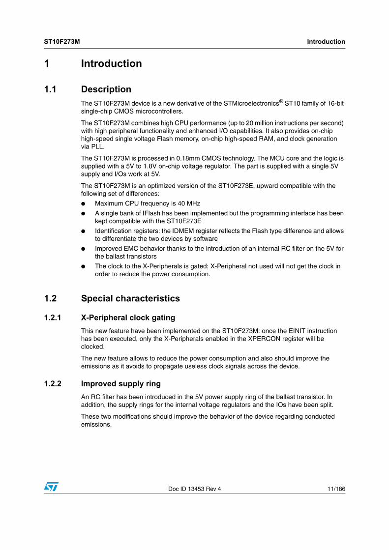
1 Introduction
1.1 Description
The ST10F273M device is a new derivative of the STMicroelectronics® ST10 family of 16-bit single-chip CMOS microcontrollers.
The ST10F273M combines high CPU performance (up to 20 million instructions per second) with high peripheral functionality and enhanced I/O capabilities. It also provides on-chip high-speed single voltage Flash memory, on-chip high-speed RAM, and clock generation via PLL.
The ST10F273M is processed in 0.18mm CMOS technology. The MCU core and the logic is supplied with a 5V to 1.8V on-chip voltage regulator. The part is supplied with a single 5V supply and I/Os work at 5V.
The ST10F273M is an optimized version of the ST10F273E, upward compatible with the following set of differences:
● Maximum CPU frequency is 40 MHz
● A single bank of IFlash has been implemented but the programming interface has been kept compatible with the ST10F273E
● Identification registers: the IDMEM register reflects the Flash type difference and allows to differentiate the two devices by software
● Improved EMC behavior thanks to the introduction of an internal RC filter on the 5V for the ballast transistors
● The clock to the X-Peripherals is gated: X-Peripheral not used will not get the clock in order to reduce the power consumption.
1.2 Special characteristics
1.2.1 X-Peripheral clock gating
This new feature have been implemented on the ST10F273M: once the EINIT instruction has been executed, only the X-Peripherals enabled in the XPERCON register will be clocked.
The new feature allows to reduce the power consumption and also should improve the emissions as it avoids to propagate useless clock signals across the device.
1.2.2 Improved supply ring
An RC filter has been introduced in the 5V power supply ring of the ballast transistor. In addition, the supply rings for the internal voltage regulators and the IOs have been split.
These two modifications should improve the behavior of the device regarding conducted emissions.
Introduction ST10F273M
12/186 Doc ID 13453 Rev 4
Figure 1. ST10F273M logic symbol

ST10F273M Pin data
Doc ID 13453 Rev 4 13/186
2 Pin data
Figure 2. Pin configuration (top view)
123456789101112131415161718192021222324252627282930313233343536
108107106105104103102101100999897969594939291908988878685848382818079787776757473
37 38 39 40 41 42 43 44 45 46 47 48 49 50 51 52 53 54 55 56 57 58 59 60 61 62 63 64 65 66 67 68 69 70 71 72
144
143
142
141
140
139
138
137
136
135
134
133
132
131
130
129
128
127
126
125
124
123
122
121
120
119
118
117
116
115
114
113
112
111
110
109
P6.0 / CS0P6.1 / CS1P6.2 / CS2P6.3 / CS3P6.4 / CS4
P6.5 / HOLD / SCLK1P6.6 / HLDA / MTSR1P6.7 / BREQ / MRST1
P8.0 / XPOUT0 / CC16IOP8.1 / XPOUT1 / CC17IOP8.2 / XPOUT2 / CC18IOP8.3 / XPOUT3 / CC19IO
P8.4 / CC20IOP8.5 / CC21IO
P8.6 / RxD1 / CC22IOP8.7 / TxD1 / CC23IO
VDDVSS
P7.0 / POUT0P7.1 / POUT1P7.2 / POUT2P7.3 / POUT3
P7.4 / CC28IOP7.5 / CC29IOP7.6 / CC30IOP7.7 / CC31IO
P5.0 / AN0P5.1 / AN1P5.2 / AN2P5.3 / AN3P5.4 / AN4P5.5 / AN5P5.6 / AN6P5.7 / AN7P5.8 / AN8P5.9 / AN9
P0H.0 / AD8P0L.7 / AD7P0L.6 / AD6P0L.5 / AD5P0L.4 / AD4P0L.3 / AD3P0L.2 / AD2P0L.1 / AD1P0L.0 / AD0EA / VSTBYALEREADYWR/WRLRDVSSVDDP4.7 / A23 / CAN2_TxD / SDAP4.6 / A22 / CAN1_TxD / CAN2_TxDP4.5 / A21 / CAN1_RxD / CAN2_RxDP4.4 / A20 / CAN2_RxD / SCLP4.3 / A19P4.2 / A18P4.1 / A17P4.0 / A16RPDVSSVDDP3.15 / CLKOUTP3.13 / SCLK0P3.12 / BHE / WRHP3.11 / RxD0P3.10 / TxD0P3.9 / MTSR0P3.8 / MRST0P3.7 / T2INP3.6 / T3IN
VA
RE
FV
AG
ND
P5.
10 /
AN
10 /
T6E
UD
P5.
11 /
AN
11 /
T5E
UD
P5.
12 /
AN
12 /
T6I
NP
5.13
/ A
N13
/ T
5IN
P5.
14 /
AN
14 /
T4E
UD
P5.
15 /
AN
15 /
T2E
UD
VS
SV
DD
P2.
0 / C
C0I
OP
2.1
/ CC
1IO
P2.
2 / C
C2I
OP
2.3
/ CC
3IO
P2.
4 / C
C4I
OP
2.5
/ CC
5IO
P2.
6 / C
C6I
OP
2.7
/ CC
7IO
VS
SV
18P
2.8
/ CC
8IO
/ E
X0I
NP
2.9
/ CC
9IO
/ E
X1I
NP
2.10
/ C
C10
IO /
EX
2IN
P2.
11 /
CC
11IO
/ E
X3I
NP
2.12
/ C
C12
IO /
EX
4IN
P2.
13 /
CC
13IO
/ E
X5I
NP
2.14
/ C
C14
IO /
EX
6IN
P2.
15 /
CC
15IO
/ E
X7I
N /
T7I
NP
3.0
/ T0I
NP
3.1
/ T6O
UT
P3.
2 / C
AP
INP
3.3
/ T3O
UT
P3.
4 / T
3EU
DP
3.5
/ T4I
NV
SS
VD
D
XT
AL4
XT
AL3
NM
IR
ST
OU
TR
ST
INV
SS
XT
AL1
XT
AL2
VD
DP
1H.7
/ A
15 /
CC
27I
P1H
.6 /
A14
/ C
C26
I P
1H.5
/ A
13 /
CC
25I
P1H
.4 /
A12
/ C
C24
IP
1H.3
/ A
11
P1H
.2 /
A10
P
1H.1
/ A
9 P
1H.0
/ A
8 V
SS
VD
DP
1L.7
/ A
7 / A
N23
P1L
.6 /
A6
/ AN
22P
1L.5
/ A
5 / A
N21
P1L
.4 /
A4
/ AN
20P
1L.3
/ A
3 / A
N19
P1L
.2 /
A2
/ AN
18P
1L.1
/ A
1 / A
N17
P1L
.0 /
A0
/ AN
16P
0H.7
/ A
D15
P0H
.6 /
AD
14P
0H.5
/ A
D13
P
0H.4
/ A
D12
P0H
.3 /
AD
11
P0H
.2 /
AD
10P
0H.1
/ A
D9
VS
SV
DD
ST10F273M

Pin data ST10F273M
14/186 Doc ID 13453 Rev 4
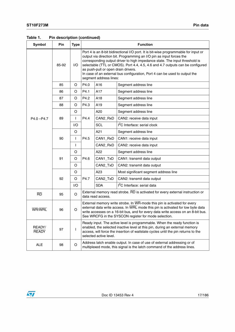
Table 1. Pin description
Symbol Pin Type Function
P6.0 - P6.7
1 - 8 I/O
8-bit bidirectional I/O port, bit-wise programmable for input or output via direction bit. Programming an I/O pin as input forces the corresponding output driver to high impedance state. Port 6 outputs can be configured as push-pull or open drain drivers. The input threshold of Port 6 is selectable (TTL or CMOS). The following Port 6 pins have alternate functions:
1 O P6.0 CS0 Chip select 0 output
... ... ... ... ...
5 O P6.4 CS4 Chip select 4 output
6I P6.5 HOLD External master hold request input
I/O SCLK1 SSC1: master clock output / slave clock input
7O P6.6 HLDA Hold acknowledge output
I/O MTSR1 SSC1: master-transmitter / slave-receiver O/I
8O P6.7 BREQ Bus request output
I/O MRST1 SSC1: master-receiver / slave-transmitter I/O
P8.0 - P8.7
9-16 I/O
8-bit bidirectional I/O port, bit-wise programmable for input or output via direction bit. Programming an I/O pin as input forces the corresponding output driver to high impedance state. Port 8 outputs can be configured as push-pull or open drain drivers. The input threshold of Port 8 is selectable (TTL or CMOS).The following Port 8 pins have alternate functions:
9I/O P8.0 CC16IO CAPCOM2: CC16 capture input / compare output
O XPWM0 PWM1: channel 0 output
... ... ... ... ...
12I/O P8.3 CC19IO CAPCOM2: CC19 capture input / compare output
O XPWM0 PWM1: channel 3 output
13 I/O P8.4 CC20IO CAPCOM2: CC20 capture input / compare output
14 I/O P8.5 CC21IO CAPCOM2: CC21 capture input / compare output
15I/O P8.6 CC22IO CAPCOM2: CC22 capture input / compare output
I/O RxD1 ASC1: Data input (Asynchronous) or I/O (Synchronous)
16I/O P8.7 CC23IO CAPCOM2: CC23 capture input / compare output
O TxD1 ASC1: Clock / Data output (Asynchronous/Synchronous)

ST10F273M Pin data
Doc ID 13453 Rev 4 15/186
P7.0 - P7.7
19-26 I/O
8-bit bidirectional I/O port, bit-wise programmable for input or output via direction bit. Programming an I/O pin as input forces the corresponding output driver to high impedance state. Port 7 outputs can be configured as push-pull or open drain drivers. The input threshold of Port 7 is selectable (TTL or CMOS).The following Port 7 pins have alternate functions:
19 O P7.0 POUT0 PWM0: channel 0 output
... ... ... ... ...
22 O P7.3 POUT3 PWM0: channel 3 output
23 I/O P7.4 CC28IO CAPCOM2: CC28 capture input / compare output
... ... ... ... ...
26 I/O P7.7 CC31IO CAPCOM2: CC31 capture input / compare output
P5.0 - P5.9P5.10 - P5.15
27-3639-44
II
16-bit input-only port with Schmitt-Trigger characteristics. The pins of Port 5 can be the analog input channels (up to 16) for the A/D converter, where P5.x equals ANx (Analog input channel x), or they are timer inputs. The input threshold of Port 5 is selectable (TTL or CMOS). The following Port 5 pins have alternate functions:
39 I P5.10 T6EUD GPT2: timer T6 external up/down control input
40 I P5.11 T5EUD GPT2: timer T5 external up/down control input
41 I P5.12 T6IN GPT2: timer T6 count input
42 I P5.13 T5IN GPT2: timer T5 count input
43 I P5.14 T4EUD GPT1: timer T4 external up/down control input
44 I P5.15 T2EUD GPT1: timer T2 external up/down control input
P2.0 - P2.7P2.8 - P2.15
47-5457-64
I/O
16-bit bidirectional I/O port, bit-wise programmable for input or output via direction bit. Programming an I/O pin as input forces the corresponding output driver to high impedance state. Port 2 outputs can be configured as push-pull or open drain drivers. The input threshold of Port 2 is selectable (TTL or CMOS).The following Port 2 pins have alternate functions:
47 I/O P2.0 CC0IO CAPCOM: CC0 capture input/compare output
... ... ... ... ...
54 I/O P2.7 CC7IO CAPCOM: CC7 capture input/compare output
57I/O
P2.8CC8IO CAPCOM: CC8 capture input/compare output
I EX0IN Fast external interrupt 0 input
... ... ... ... ...
64
I/O
P2.15
CC15IO CAPCOM: CC15 capture input/compare output
I EX7IN Fast external interrupt 7 input
I T7IN CAPCOM2: timer T7 count input
Table 1. Pin description (continued)
Symbol Pin Type Function
Pin data ST10F273M
16/186 Doc ID 13453 Rev 4
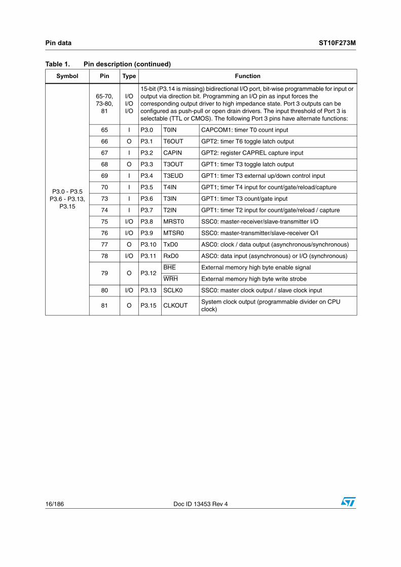
P3.0 - P3.5P3.6 - P3.13,
P3.15
65-70,73-80,
81
I/OI/OI/O
15-bit (P3.14 is missing) bidirectional I/O port, bit-wise programmable for input or output via direction bit. Programming an I/O pin as input forces the corresponding output driver to high impedance state. Port 3 outputs can be configured as push-pull or open drain drivers. The input threshold of Port 3 is selectable (TTL or CMOS). The following Port 3 pins have alternate functions:
65 I P3.0 T0IN CAPCOM1: timer T0 count input
66 O P3.1 T6OUT GPT2: timer T6 toggle latch output
67 I P3.2 CAPIN GPT2: register CAPREL capture input
68 O P3.3 T3OUT GPT1: timer T3 toggle latch output
69 I P3.4 T3EUD GPT1: timer T3 external up/down control input
70 I P3.5 T4IN GPT1; timer T4 input for count/gate/reload/capture
73 I P3.6 T3IN GPT1: timer T3 count/gate input
74 I P3.7 T2IN GPT1: timer T2 input for count/gate/reload / capture
75 I/O P3.8 MRST0 SSC0: master-receiver/slave-transmitter I/O
76 I/O P3.9 MTSR0 SSC0: master-transmitter/slave-receiver O/I
77 O P3.10 TxD0 ASC0: clock / data output (asynchronous/synchronous)
78 I/O P3.11 RxD0 ASC0: data input (asynchronous) or I/O (synchronous)
79 O P3.12BHE External memory high byte enable signal
WRH External memory high byte write strobe
80 I/O P3.13 SCLK0 SSC0: master clock output / slave clock input
81 O P3.15 CLKOUTSystem clock output (programmable divider on CPU clock)
Table 1. Pin description (continued)
Symbol Pin Type Function
ST10F273M Pin data
Doc ID 13453 Rev 4 17/186
P4.0 –P4.7
85-92 I/O
Port 4 is an 8-bit bidirectional I/O port. It is bit-wise programmable for input or output via direction bit. Programming an I/O pin as input forces the corresponding output driver to high impedance state. The input threshold is selectable (TTL or CMOS). Port 4.4, 4.5, 4.6 and 4.7 outputs can be configured as push-pull or open drain drivers.In case of an external bus configuration, Port 4 can be used to output the segment address lines:
85 O P4.0 A16 Segment address line
86 O P4.1 A17 Segment address line
87 O P4.2 A18 Segment address line
88 O P4.3 A19 Segment address line
89
O
P4.4
A20 Segment address line
I CAN2_RxD CAN2: receive data input
I/O SCL I2C Interface: serial clock
90
O
P4.5
A21 Segment address line
I CAN1_RxD CAN1: receive data input
I CAN2_RxD CAN2: receive data input
91
O
P4.6
A22 Segment address line
O CAN1_TxD CAN1: transmit data output
O CAN2_TxD CAN2: transmit data output
92
O
P4.7
A23 Most significant segment address line
O CAN2_TxD CAN2: transmit data output
I/O SDA I2C Interface: serial data
RD 95 OExternal memory read strobe. RD is activated for every external instruction or data read access.
WR/WRL 96 O
External memory write strobe. In WR-mode this pin is activated for every external data write access. In WRL mode this pin is activated for low byte data write accesses on a 16-bit bus, and for every data write access on an 8-bit bus. See WRCFG in the SYSCON register for mode selection.
READY/READY
97 I
Ready input. The active level is programmable. When the ready function is enabled, the selected inactive level at this pin, during an external memory access, will force the insertion of waitstate cycles until the pin returns to the selected active level.
ALE 98 OAddress latch enable output. In case of use of external addressing or of multiplexed mode, this signal is the latch command of the address lines.
Table 1. Pin description (continued)
Symbol Pin Type Function

Pin data ST10F273M
18/186 Doc ID 13453 Rev 4
EA / VSTBY 99 I
External access enable pin.
A low level applied to this pin during and after Reset forces the ST10F273M to start the program from the external memory space. A high level forces ST10F273M to start in the internal memory space. This pin is also used (when Standby mode is entered, that is ST10F273M under reset and main VDD turned off) to bias the 32 kHz oscillator amplifier circuit and to provide a reference voltage for the low-power embedded voltage regulator which generates the internal 1.8V supply for the RTC module (when not disabled) and to retain data inside the Standby portion of the XRAM (16 Kbyte).
It can range from 4.5 to 5.5V (6V for a reduced amount of time during the device life, 4.0V when RTC and 32 kHz on-chip oscillator amplifier are turned off). In running mode, this pin can be tied low during reset without affecting 32 kHz oscillator, RTC and XRAM activities, since the presence of a stable VDD guarantees the proper biasing of all those modules.
P0L.0 -P0L.7,P0H.0
P0H.1 - P0H.7
100-107,108,
111-117I/O
Two 8-bit bidirectional I/O ports P0L and P0H, bit-wise programmable for input or output via direction bit. Programming an I/O pin as input forces the corresponding output driver to high impedance state. The input threshold of Port 0 is selectable (TTL or CMOS).
In case of an external bus configuration, PORT0 serves as the address (A) and as the address / data (AD) bus in multiplexed bus modes and as the data (D) bus in demultiplexed bus modes.
Demultiplexed bus modes
Multiplexed bus modes
P1L.0 - P1L.7P1H.0 - P1H.7
118-125128-135
I/O
Two 8-bit bidirectional I/O ports P1L and P1H, bit-wise programmable for input or output via direction bit. Programming an I/O pin as input forces the corresponding output driver to high impedance state. PORT1 is used as the 16-bit address bus (A) in demultiplexed bus modes: if at least BUSCONx is configured such the demultiplexed mode is selected, the pis of PORT1 are not available for general purpose I/O function. The input threshold of Port 1 is selectable (TTL or CMOS).
The pins of P1L also serve as the additional (up to 8) analog input channels for the A/D converter, where P1L.x equals ANy (Analog input channel y, where y = x + 16). This additional function have higher priority on demultiplexed bus function. The following PORT1 pins have alternate functions:
132 I P1H.4 CC24IO CAPCOM2: CC24 capture input
133 I P1H.5 CC25IO CAPCOM2: CC25 capture input
134 I P1H.6 CC26IO CAPCOM2: CC26 capture input
135 I P1H.7 CC27IO CAPCOM2: CC27 capture input
Table 1. Pin description (continued)
Symbol Pin Type Function
Data path width 8-bit 16-bit
P0L.0 – P0L.7: D0 – D7 D0 - D7
P0H.0 – P0H.7: I/O D8 - D15
Data path width 8-bit 16-bit
P0L.0 – P0L.7: AD0 – AD7 AD0 - AD7
P0H.0 – P0H.7: A8 – A15 AD8 - AD15
ST10F273M Pin data
Doc ID 13453 Rev 4 19/186
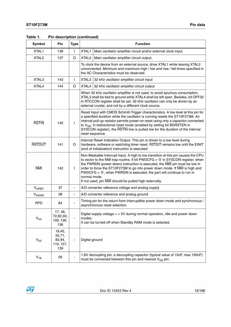
XTAL1 138 I XTAL1 Main oscillator amplifier circuit and/or external clock input.
XTAL2 137 O XTAL2 Main oscillator amplifier circuit output.
To clock the device from an external source, drive XTAL1 while leaving XTAL2 unconnected. Minimum and maximum high / low and rise / fall times specified in the AC Characteristics must be observed.
XTAL3 143 I XTAL3 32 kHz oscillator amplifier circuit input
XTAL4 144 O XTAL4 32 kHz oscillator amplifier circuit output
When 32 kHz oscillator amplifier is not used, to avoid spurious consumption, XTAL3 shall be tied to ground while XTAL4 shall be left open. Besides, bit OFF32 in RTCCON register shall be set. 32 kHz oscillator can only be driven by an external crystal, and not by a different clock source.
RSTIN 140 I
Reset Input with CMOS Schmitt-Trigger characteristics. A low level at this pin for a specified duration while the oscillator is running resets the ST10F273M. An internal pull-up resistor permits power-on reset using only a capacitor connected to VSS. In bidirectional reset mode (enabled by setting bit BDRSTEN in SYSCON register), the RSTIN line is pulled low for the duration of the internal reset sequence.
RSTOUT 141 OInternal Reset Indication Output. This pin is driven to a low level during hardware, software or watchdog timer reset. RSTOUT remains low until the EINIT (end of initialization) instruction is executed.
NMI 142 I
Non-Maskable Interrupt Input. A high to low transition at this pin causes the CPU to vector to the NMI trap routine. If bit PWDCFG = ‘0’ in SYSCON register, when the PWRDN (power down) instruction is executed, the NMI pin must be low in order to force the ST10F273M to go into power down mode. If NMI is high and PWDCFG = ‘0’, when PWRDN is executed, the part will continue to run in normal mode.If not used, pin NMI should be pulled high externally.
VAREF 37 - A/D converter reference voltage and analog supply
VAGND 38 - A/D converter reference and analog ground
RPD 84 -Timing pin for the return from interruptible power down mode and synchronous / asynchronous reset selection.
VDD
17, 46, 72,82,93, 109, 126,
136
-Digital supply voltage = + 5V during normal operation, idle and power down modes. It can be turned off when Standby RAM mode is selected.
VSS
18,45, 55,71, 83,94,
110, 127, 139
- Digital ground
V18 56 -1.8V decoupling pin: a decoupling capacitor (typical value of 10nF, max 100nF) must be connected between this pin and nearest VSS pin.
Table 1. Pin description (continued)
Symbol Pin Type Function
Functional description ST10F273M
20/186 Doc ID 13453 Rev 4
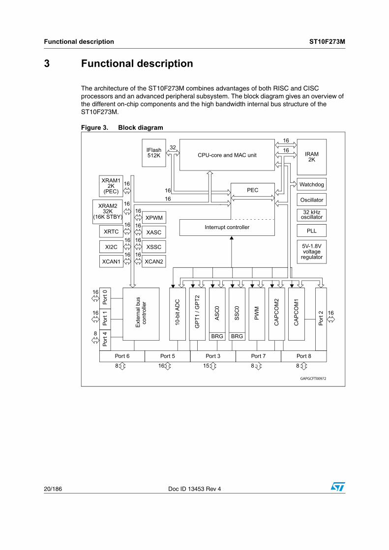
3 Functional description
The architecture of the ST10F273M combines advantages of both RISC and CISC processors and an advanced peripheral subsystem. The block diagram gives an overview of the different on-chip components and the high bandwidth internal bus structure of the ST10F273M.
Figure 3. Block diagram
ST10F273M Memory organization
Doc ID 13453 Rev 4 21/186
4 Memory organization
The memory space of the ST10F273M is configured in a unified memory architecture. Code memory, data memory, registers and I/O ports are organized within the same linear address space of 16 Mbytes. The entire memory space can be accessed Bytewise or Wordwise. Particular portions of the on-chip memory have additionally been made directly bit addressable.
IFlash: 512 Kbytes of on-chip Flash memory implemented as a unique Bank (Bank0). Bank0 is divided in 12 blocks (B0F0...B0F11).
Note: Read-while-write operations are not allowed: Write commands must be executed from a non IFlash memory area (on-chip RAM or external memory).
When Bootstrap mode is selected, the Test-Flash Block B0TF (4 Kbytes) appears at address 00’0000h: Refer to the device User Manual for more details on the memory mapping in Bootstrap mode. The summary of address range for IFlash is the following:
Note: A single Flash bank is implemented on the ST10F273M compared to the ST10F273E. The last two sectors (B0F10 and B0F11) can be seen as the Bank1 of the ST10F273E in order to maintain the compatibility with the existing Flash programming drivers. For this, the control and status bit of the blocks B0F10 and B0F11 have been duplicated to be usable as blocks B1F0 and B1F1 of the ST10F273E.
XFLASH / Flash Control Registers: Address range 0E’0000h-0E’FFFFh is reserved for the Flash Control Register and other internal service memory space used by the Flash Program/Erase Controller. XFLASHEN bit in XPERCON register must be set to access the Flash Control Register. Note that when Flash Control Registers are not accessible, no program/erase operations are possible. The Flash Control Registers are accessed in 16-bit demultiplexed bus-mode without read/write delay. Byte and word accesses are allowed.
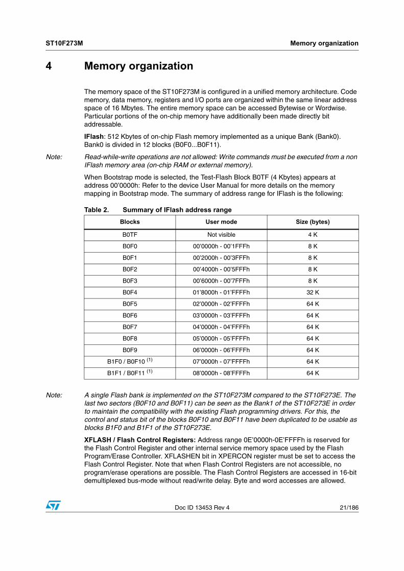
Table 2. Summary of IFlash address range
Blocks User mode Size (bytes)
B0TF Not visible 4 K
B0F0 00’0000h - 00’1FFFh 8 K
B0F1 00’2000h - 00’3FFFh 8 K
B0F2 00’4000h - 00’5FFFh 8 K
B0F3 00’6000h - 00’7FFFh 8 K
B0F4 01’8000h - 01’FFFFh 32 K
B0F5 02’0000h - 02’FFFFh 64 K
B0F6 03’0000h - 03’FFFFh 64 K
B0F7 04’0000h - 04’FFFFh 64 K
B0F8 05’0000h - 05’FFFFh 64 K
B0F9 06’0000h - 06’FFFFh 64 K
B1F0 / B0F10 (1) 07’0000h - 07’FFFFh 64 K
B1F1 / B0F11 (1) 08’0000h - 08’FFFFh 64 K

Memory organization ST10F273M
22/186 Doc ID 13453 Rev 4
IRAM: 2 Kbytes of on-chip internal RAM (dual-port) is provided as a storage for data, system stack, general purpose register banks and code. A register bank is 16 Wordwide (R0 to R15) and / or Bytewide (RL0, RH0, …, RL7, RH7) general purpose registers group.
XRAM: 34 Kbytes of on-chip extension RAM (single port XRAM) is provided as a storage for data, user stack and code.The XRAM is divided into two areas, the first 2 Kbytes named XRAM1 and the second 32 Kbytes named XRAM2, connected to the internal XBUS and are accessed like an external memory in 16-bit demultiplexed bus-mode without wait state or read/write delay (50ns access at 40 MHz CPU clock). Byte and Word accesses are allowed.
The XRAM1 address range is 00’E000h - 00’E7FFh if XPEN (bit 2 of SYSCON register), and XRAM1EN (bit 2 of XPERCON register) are set.If XRAM1EN or XPEN is cleared, then any access in the address range 00’E000h -00’E7FFh will be directed to external memory interface, using the BUSCONx register corresponding to address matching ADDRSELx register.
The XRAM2 address range is F’0000h - F’7FFFFh if XPEN (bit 2 of SYSCON register), and XRAM2EN (bit 3 of XPERCON register) are set.If bit XPEN is cleared, then any access in the address range programmed for XRAM2 will be directed to external memory interface, using the BUSCONx register corresponding to address matching ADDRSELx register.
The 16 kbytes lower portion of the XRAM2 (address range F’0000h - F’3FFFFh) represents also the Standby RAM, which can be maintained biased through EA / VSTBY pin when the main supply VDD is turned off.As the XRAM appears like external memory, it cannot be used as system stack or as register banks. The XRAM is not provided for single bit storage and therefore is not bit addressable.
SFR/ESFR: 1024 bytes (2 x 512 bytes) of address space is reserved for the special function register (SFR) areas. SFRs are Wordwide registers which are used to control and to monitor the function of the different on-chip units.
CAN1: Address range 00’EF00h - 00’EFFFh is reserved for the CAN1 Module access. The CAN1 is enabled by setting XPEN bit 2 of the SYSCON register and by setting CAN1EN bit 0 of the XPERCON register. Accesses to the CAN Module use demultiplexed addresses and a 16-bit data bus (only word accesses are possible). Two wait states give an access time of 100ns at 40 MHz CPU clock. No tri-state wait states are used.
CAN2: Address range 00’EE00h - 00’EEFFh is reserved for the CAN2 Module access. The CAN2 is enabled by setting XPEN bit 2 of the SYSCON register and by setting CAN2EN bit 1 of the new XPERCON register. Accesses to the CAN Module use demultiplexed addresses and a 16-bit data bus (only word accesses are possible). Two wait states give an access time of 100ns at 40 MHz CPU clock. No tri-state wait states are used.
Note: If one or the two CAN modules are used, Port 4 cannot be programmed to output all eight segment address lines. Thus, only four segment address lines can be used, reducing the external memory space to 5 Mbytes (1 Mbyte per CS line).
RTC: Address range 00’ED00h - 00’EDFFh is reserved for the RTC Module access. The RTC is enabled by setting XPEN bit 2 of the SYSCON register and bit 4 of the XPERCON register. Accesses to the RTC Module use demultiplexed addresses and a 16-bit data bus (only word accesses are possible). Two waitstates give an access time of 100ns at 40 MHz CPU clock. No tristate waitstate is used.

ST10F273M Memory organization
Doc ID 13453 Rev 4 23/186
PWM1: Address range 00’EC00h - 00’ECFFh is reserved for the PWM1 Module access. The PWM1 is enabled by setting XPEN bit 2 of the SYSCON register and bit 6 of the XPERCON register. Accesses to the PWM1 Module use demultiplexed addresses and a 16-bit data bus (only word accesses are possible). Two waitstates give an access time of 100ns at 40 MHz CPU clock. No tristate waitstate is used. Only word access is allowed.
ASC1: Address range 00’E900h - 00’E9FFh is reserved for the ASC1 Module access. The ASC1 is enabled by setting XPEN bit 2 of the SYSCON register and bit 7 of the XPERCON register. Accesses to the ASC1 Module use demultiplexed addresses and a 16-bit data bus (only word accesses are possible). Two waitstates give an access time of 100ns at 40 MHz CPU clock. No tristate waitstate is used.
SSC1: Address range 00’E800h - 00’E8FFh is reserved for the SSC1 Module access. The SSC1 is enabled by setting XPEN bit 2 of the SYSCON register and bit 8 of the XPERCON register. Accesses to the SSC1 Module use demultiplexed addresses and a 16-bit data bus (only word accesses are possible). Two waitstates give an access time of 100ns at 40 MHz CPU clock. No tristate waitstate is used.
I2C: Address range 00’EA00h - 00’EAFFh is reserved for the I2C Module access. The I2C is enabled by setting XPEN bit 2 of the SYSCON register and bit 9 of the XPERCON register. Accesses to the I2C Module use demultiplexed addresses and a 16-bit data bus (only word accesses are possible). Two waitstates give an access time of 100ns at 40 MHz CPU clock. No tristate waitstate is used.
X-Miscellaneous: Address range 00’EB00h - 00’EBFFh is reserved for the access to a set of XBUS additional features. They are enabled by setting XPEN bit 2 of the SYSCON register and bit 10 of the XPERCON register. Accesses to this additional features use demultiplexed addresses and a 16-bit data bus (only word accesses are possible). Two waitstates give an access time of 100ns at 40 MHz CPU clock. No tristate waitstate is used. The following set of features are provided:
● CLKOUT programmable divider
● XBUS interrupt management registers
● ADC multiplexing on P1L register
● Port1L digital disable register for extra ADC channels
● CAN2 multiplexing on P4.5/P4.6
● CAN1-2 main clock prescaler
● Main Voltage Regulator disable for power-down mode
● TTL / CMOS threshold selection for Port0, Port1 and Port5
In order to meet the needs of designs where more memory is required than is provided on chip, up to 16 Mbytes of external memory can be connected to the microcontroller.
Visibility of XBUS peripherals
In order to keep the ST10F273M compatible with the ST10F168 / ST10F269, the XBUS peripherals can be selected to be visible on the external address / data bus. Different bits for X-Peripheral enabling in XPERCON register must be set. If these bits are cleared before the global enabling with XPEN bit in SYSCON register, the corresponding address space, port pins and interrupts are not occupied by the peripherals, thus the peripheral is not visible and not available. Refer to Chapter 23: Register set on page 115.

Memory organization ST10F273M
24/186 Doc ID 13453 Rev 4
XPERCON and X-Peripheral clock gating
As already mentioned, the XPERCON register must be programmed to enable the single XBus modules separately. The XPERCON is a read/write ESFR register.
The new feature of Clock Gating has been implemented by means of this register: Once the EINIT instruction has been executed, all the peripherals (except RAMs and XMISC) not enabled in the XPERCON register are not be clocked. The clock gating can reduce power consumption and improve EMI when the user does not use all X-Peripherals.
Note: When the clock has been gated in the disabled peripherals, no Reset will be raised once the EINIT instruction has been executed.

ST10F273M Memory organization
Doc ID 13453 Rev 4 25/186
Figure 4. ST10F273M memory mapping (XADRS3 = 800Bh - reset value)
Ext. MemB0F3
Ext. Mem
Reserved
B3F1(XFLASH)
(XFLASH)B2F2
XSSCXASCXI2C
XPWM
XI2C
XASC
XSSC
FF FFFF
00 0000
16 MB
255
0
Code DataPage
1023
0
DataPage
1
3
5
7
1
23456789
10111213141516171819
07 FFFF
06 000005 FFFF
04 000003 FFFF
02 000001 FFFF
00 0000
B0F4
B0F5
B0F8
B0F11
00 C000
00 FFFF
XCAN1
ESFR
SFR
I-RAM
Reserved
Ext. Memory
00 DFFF00 E000
00 E7FF00 E800
00 FDFF00 FE00
00 F1FF00 F200
00 F5FF00 F600
8K
256
512
1K
2K
512
Data Page 3 (Segment 0) - 16Kbyte
256XCAN2
9
20212223
0A 000009 FFFF
08 0000
11
24252627
0C 00000B FFFF
13
28293031
0E 00000D FFFF
15
32333435
0F FFFF
00 F000
XCAN1
XCAN2
00 EFFF00 F000
00 EEFF00 EF00
00 EDFF00 EE00
00 EAFF00 EB00
256
256
256
256
00 E7FF00 E800
XRAM1 2K
14
0F 00000E FFFF
12
0D 00000C FFFF
10
0B 00000A FFFF
8
6
4
05 000004 FFFF
07 000006 FFFF
09 000008 FFFF
2
03 000002 FFFF
0
0
36373839404142434445464748495051525354555657585960616263
B0F6
B0F9
B0F10
B2F1
B0F7
01 000000 FFFF
XRAM2 32K
B3F0
CodeSegment
6465666764656667
16
17
10 0000
10 FFFF11 0000
11 FFFF
Flash + XRAM - 1Mbyte
Flash
XRTC00 EFFF
(XFLASH)
(XFLASH)
256256
256
XRTC
256
256
00 E8FF00 E900
00 E9FF00 EA00
(StandBy)
256 00 ECFF00 ED00
256
256 XPWM256
25600 EBFF00 EC00XMiscellaneous
XMiscellaneous
X-Peripherals (2Kbyte)
Segment
XA
DR
S3
= 8
00B
h (5
12K
- D
efau
lt)
Reserved
B2F0(XFLASH)
Reserved
Reserved
Reserved
Reserved
64K
Address Area defined by XADRS3 by default after reset
(B1F0)
(B1F1)
ControlRegisters
B0F2B0F1B0F0

Memory organization ST10F273M
26/186 Doc ID 13453 Rev 4
Figure 5. ST10F273M memory mapping (XADRS3 = E009h - user programmed value)
XSSCXASCXI2C
XPWM
XI2C
XASC
XSSC
FF FFFF
00 0000
16 MB
255
0
Code DataPage
1023
0
DataPage
1
3
5
7
1
2
3456789
10111213141516171819
07 FFFF
06 000005 FFFF
04 000003 FFFF
02 000001 FFFF
00 0000
B0F4
B0F5
B0F8
B0F11
00 C000
00 FFFF
XCAN1
ESFR
SFR
I-RAM
Reserved
Ext. Memory
00 DFFF00 E000
00 E7FF00 E800
00 FDFF00 FE00
00 F1FF00 F200
00 F5FF00 F600
8K
256
512
1K
2K
512
Data Page 3 (Segment 0) - 16Kbyte
256XCAN2
9
20212223
0A 000009 FFFF
08 0000
11
24252627
0C 00000B FFFF
13
28293031
0E 00000D FFFF
15
32333435
0F FFFF
00 F000
XCAN1
XCAN2
00 EFFF00 F000
00 EEFF00 EF00
00 EDFF00 EE00
00 EAFF00 EB00
256
256
256
256
00 E7FF00 E800
XRAM1 2K
14
0F 00000E FFFF
12
0D 00000C FFFF
10
0B 00000A FFFF
8
6
4
05 000004 FFFF
07 000006 FFFF
09 000008 FFFF
2
03 000002 FFFF
0
0
B0F3
36373839404142434445464748495051525354555657585960616263
B0F6
B0F9
B0F10
B0F7
01 000000 FFFF
XRAM232K
CodeSegment
6465666764656667
16
17
10 0000
10 FFFF11 0000
11 FFFF
Flash + XRAM - 1Mbyte
Flash
XRTC00 EFFF
256256
256
XRTC
256
256
00 E8FF00 E900
00 E9FF00 EA00
(StandBy)
256 00 ECFF00 ED00
256
256 XPWM256
25600 EBFF00 EC00XMiscellaneous
XMiscellaneous
X-Peripherals (2Kbyte)
Segment
XA
DR
S3
= E
009hReserved
64K
Address Area defined by XADRS3 after reprogramming
Note: E009h defines a 128K wide window starting from 0E’0000h
(B1F0)
(B1F1)
ControlRegisters
32K
ExtMemory
B0F2B0F1B0F0
Ext Mem
Ext Mem

ST10F273M Internal Flash memory
Doc ID 13453 Rev 4 27/186
5 Internal Flash memory
5.1 Overview
The on-chip Flash is composed of one matrix module of one bank of 512 Kbytes, named Bank0, that can be read and modified. This module is called IFlash because it is on the ST10 Internal bus.
Figure 6. Flash structure
The programming operations of the Flash are managed by an embedded Flash Program/Erase Controller (FPEC). The high voltages needed for Program/Erase operations are generated internally.
The Data bus is 32-bit wide for fetch accesses to IFlash. Read/write accesses to IFlash Control Registers area are 16-bit wide.
5.2 Functional description
5.2.1 Structure
Table 3 below shows the address space reserved for the Flash module.
5.2.2 Module structure
The IFlash module is composed of a bank (Bank 0) of 512 Kbytes of program memory divided in 12 sectors (B0F0...B0F11). Bank 0 also contains a reserved sector named Test-Flash.
Table 3. Flash module address space
Description Addresses Size
IFlash sectors 0x00 0000 to 0x08 FFFF 512 Kbytes
Registers and Flash internal reserved area 0x0E 0000 to 0x0E FFFF 64 Kbytes
Internal Flash memory ST10F273M
28/186 Doc ID 13453 Rev 4
The Addresses from 0x0E 0000 to 0x0E FFFF are reserved for the Control Register Interface and other internal service memory space used by the Flash Program/Erase controller.
The following tables show the memory mapping of the Flash when it is accessed in read mode (Table 4: Flash module sectorization (read operations)), and when accessed in write or erase mode (Table 5: Flash module sectorization (write operations, or ROMS1 = ‘1’)).
Note: With this second mapping, the first four sectors are remapped into code segment 1 (same as obtained setting bit ROMS1 in SYSCON register).
Table 4. Flash module sectorization (read operations)
Bank Description Addresses Size (bytes)
B0
Bank 0 Flash 0 (B0F0) 0x00 0000 - 0x00 1FFF 8 K
Bank 0 Flash 1 (B0F1) 0x00 2000 - 0x00 3FFF 8 K
Bank 0 Flash 2 (B0F2) 0x00 4000 - 0x00 5FFF 8 K
Bank 0 Flash 3 (B0F3) 0x00 6000 - 0x00 7FFF 8 K
Bank 0 Flash 4 (B0F4) 0x01 8000 - 0x01 FFFF 32 K
Bank 0 Flash 5 (B0F5) 0x02 0000 - 0x02 FFFF 64 K
Bank 0 Flash 6 (B0F6) 0x03 0000 - 0x03 FFFF 64 K
Bank 0 Flash 7 (B0F7) 0x04 0000 - 0x04 FFFF 64 K
Bank 0 Flash 8 (B0F8) 0x05 0000 - 0x05 FFFF 64 K
Bank 0 Flash 9 (B0F9) 0x06 0000 - 0x06 FFFF 64 K
Bank 0 Flash 10 (B0F10 / B1F0) (1)
1. A single bank is implemented but the last two sectors can be seen as a Bank 1 in order to maintain compatibility with the Flash Programming routines developed for the ST10F273E (based on ST10F276E). This means that the Control and Status flags for the blocks B0F10 and B0F11 are duplicated to also be accessible as blocks B1F0 and B1F1.
0x07 0000 - 0x07 FFFF 64 K
Bank 0 Flash 11 (B0F11 / B1F1) (1) 0x08 0000 - 0x08 FFFF 64 K

ST10F273M Internal Flash memory
Doc ID 13453 Rev 4 29/186
Table 5 above refers to the configuration when bit ROMS1 of SYSCON register is set.
When Bootstrap mode is entered:
● Test-Flash is seen and available for code fetches (address 0x00 0000)
● User IFlash is only available for read and write accesses
● Write accesses must be made with addresses starting in segment 1 from 0x01 0000, whatever ROMS1 bit in SYSCON value
● Read accesses are made in segment 0 or in segment 1 depending of ROMS1 value.
In Bootstrap mode, by default ROMS1 = 0, so the first 32 Kbytes of IFlash are mapped in segment 0.
Example 1:In default configuration, to program address 0, the user must put the value 0x01 0000 in the FARL and FARH registers but to verify the content of the address 0, a read to 0x00 0000 must be performed.
The next Table 6 shows the Control Register interface composition: This set of registers can be addressed by the CPU .
Table 5. Flash module sectorization (write operations, or ROMS1 = ‘1’)
Bank Description Addresses Size (bytes)
B0
Bank 0 Test-Flash (B0TF) 0x00 0000 - 0x00 0FFF 4 K
Bank 0 Flash 0 (B0F0) 0x01 0000 - 0x01 1FFF 8 K
Bank 0 Flash 1 (B0F1) 0x01 2000 - 0x01 3FFF 8 K
Bank 0 Flash 2 (B0F2) 0x01 4000 - 0x01 5FFF 8 K
Bank 0 Flash 3 (B0F3) 0x01 6000 - 0x01 7FFF 32 K
Bank 0 Flash 4 (B0F4) 0x01 8000 - 0x01 FFFF 64 K
Bank 0 Flash 5 (B0F5) 0x02 0000 - 0x02 FFFF 64 K
Bank 0 Flash 6 (B0F6) 0x03 0000 - 0x03 FFFF 64 K
Bank 0 Flash 7 (B0F7) 0x04 0000 - 0x04 FFFF 64 K
Bank 0 Flash 8 (B0F8) 0x05 0000 - 0x05 FFFF 64 K
Bank 0 Flash 9 (B0F9) 0x06 0000 - 0x06 FFFF 64 K
Bank 0 Flash 10 (B0F10 / B1F0) (1)
1. A single bank is implemented but the last two sectors can be seen as a Bank 1 in order to maintain compatibility with the Flash Programming routines developed for the ST10F273E (based on ST10F276E). This means that the Control and Status flags for the blocks B0F10 and B0F11 are duplicated to also be accessible as blocks B1F0 and B1F1.
0x07 0000 - 0x07 FFFF 64 K
Bank 0 Flash 11 (B0F11 / B1F1) (1) 0x08 0000 - 0x08 FFFF 8 K

Internal Flash memory ST10F273M
30/186 Doc ID 13453 Rev 4
Note: FVWPIR-mirror is a mirror of the FVWPIR to maintain software compatibility with the ST10F273E in the handling of the last two blocks B0F10/B1F0 and B0F11/B1F1.
XFICR is a dummy register that can be read and written (for compatibility with the ST10F273E) but its content has no effect on the XBus timings.
5.2.3 Low power mode
The Flash module is automatically switched off executing PWRDN instruction. The consumption is drastically reduced, but exiting this state can require a long time (tPD).
Recovery time from Power-down mode for the Flash modules is anyway shorter than the main oscillator start-up time. To avoid any problem in restarting to fetch code from the Flash, it is important to size properly the external circuit on RPD pin.
Note: PWRDN instruction must not be executed while a Flash program/erase operation is in progress.
5.3 Write operation
The Flash module has a single register interface mapped in the XBus memory space 0x0E 0000 - 0x0E 0015. All the operations are enabled through four 16-bit control registers: Flash Control Register 1-0 High/Low (FCR1H/L-FCR0H/L). Eight other 16-bit registers are used to store Flash Address and Data for Program operations (FARH/L and FDR1H/L-FDR0H/L) and Write Operation Error flags (FER). All registers are accessible with 8- and 16-bit instructions (since they are mapped on the XBus).
Note: To have access to the Flash Control Registers used for program/erasing operations, bit 5 (XFLASHEN) in XPERCON register must be set.
Table 6. Flash control registers summary
Name Description Addresses Size Bus size
FCR1 - 0Flash control registers 1 - 0 High & Low
0x0E 0000 - 0x0E 0007 8 byte
16-bit (XBus)
FDR1 - 0Flash data registers 1 - 0 High & Low
0x0E 0008 - 0x0E 000F 8 byte
FAR Flash address registers 0x0E 0010 - 0x0E 0013 4 byte
FER Flash error register 0x0E 0014 - 0x0E 0015 2 byte
FVWPIR-mirrorFlash non-volatile protection I registers mirrored
0x0E DFB0 - 0x0E DFB3 4 byte
FVWPIR Flash volatile protection I registers 0x0E DFB4 - 0x0E DFB7 4 byte
FVAPR0Flash volatile access protection register 0
0x0E DFB8 - 0x0E DFB9 2 byte
FVAPR1Flash non-volatile access protection register 1
0x0E DFBC - 0x0E DFBF 4 byte
XFICRXFlash Interface Control register (dummy register)
0x0E E000 - 0x0E E001 2 byte
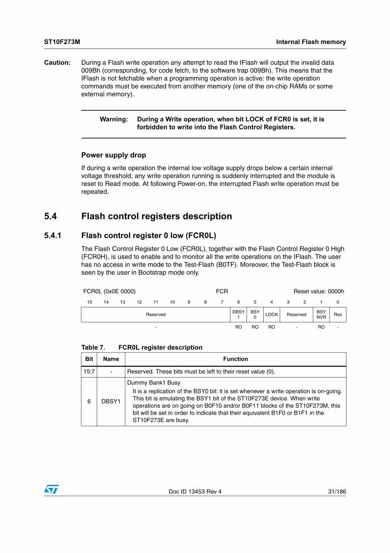
ST10F273M Internal Flash memory
Doc ID 13453 Rev 4 31/186
Caution: During a Flash write operation any attempt to read the IFlash will output the invalid data 009Bh (corresponding, for code fetch, to the software trap 009Bh). This means that the IFlash is not fetchable when a programming operation is active: the write operation commands must be executed from another memory (one of the on-chip RAMs or some external memory).
Warning: During a Write operation, when bit LOCK of FCR0 is set, it is forbidden to write into the Flash Control Registers.
Power supply drop
If during a write operation the internal low voltage supply drops below a certain internal voltage threshold, any write operation running is suddenly interrupted and the module is reset to Read mode. At following Power-on, the interrupted Flash write operation must be repeated.
5.4 Flash control registers description
5.4.1 Flash control register 0 low (FCR0L)
The Flash Control Register 0 Low (FCR0L), together with the Flash Control Register 0 High (FCR0H), is used to enable and to monitor all the write operations on the IFlash. The user has no access in write mode to the Test-Flash (B0TF). Moreover, the Test-Flash block is seen by the user in Bootstrap mode only.
FCR0L (0x0E 0000) FCR Reset value: 0000h
15 14 13 12 11 10 9 8 7 6 5 4 3 2 1 0
Reserved DBSY1
BSY0 LOCK Reserved BSY
NVR Res
- RO RO RO - RO -
Table 7. FCR0L register description
Bit Name Function
15:7 - Reserved. These bits must be left to their reset value (0).
6 DBSY1
Dummy Bank1 Busy
It is a replication of the BSY0 bit: it is set whenever a write operation is on-going.This bit is emulating the BSY1 bit of the ST10F273E device. When write operations are on going on B0F10 and/or B0F11 blocks of the ST10F273M, this bit will be set in order to indicate that their equivalent B1F0 or B1F1 in the ST10F273E are busy.

Internal Flash memory ST10F273M
32/186 Doc ID 13453 Rev 4
5 BSY0
Bank0 Busy
This bits indicate that a write operation is running in the Bank0. It is automatically set when bit WMS is set. When this bit is set every read access to the Bank0 will output invalid data (software trap 009Bh), while every write access will be ignored. At the end of the write operation or during a Program or Erase Suspend this bit is automatically reset and Flash Bank returns to read mode. After a Program or Erase Resume this bit is automatically set again.
4 LOCK
Flash registers access locked
When this bit is set, it means that the access to the Flash Control Registers FCR0H/-FCR1H/L, FDR0H/L-FDR1H/L, FARH/L and FER is locked by the FPEC: any read access to the registers will output invalid data (software trap 009Bh) and any write access will be ineffective. LOCK bit is automatically set when the Flash bit WMS is set.This is the only bit the user can always access to detect the status of the Flash: once it is found low, the rest of FCR0L and all the other Flash registers are accessible by the user as well.Note that FER content can be read when LOCK is low, but its content is updated only when also BSYx bits are reset.
3:2 - Reserved. These bits must be left to their reset value (0).
1 BSYNVR
Busy of Non-Volatile RegistersThis bit indicate that a write operation is running in the corresponding on “Non-volatile registers”. They are automatically set when bit WMS is set. When this bit is set every read access to the IFlash will output the value 009Bh (software trap), while every write access to the IFlash will be ignored. At the end of the write operation or during a Program Suspend this bit is automatically reset and the IFlash returns to read mode. After a Program this bit is automatically set again.
0 - Reserved. This bit must be left to its reset value (0).
Table 7. FCR0L register description (continued)
Bit Name Function
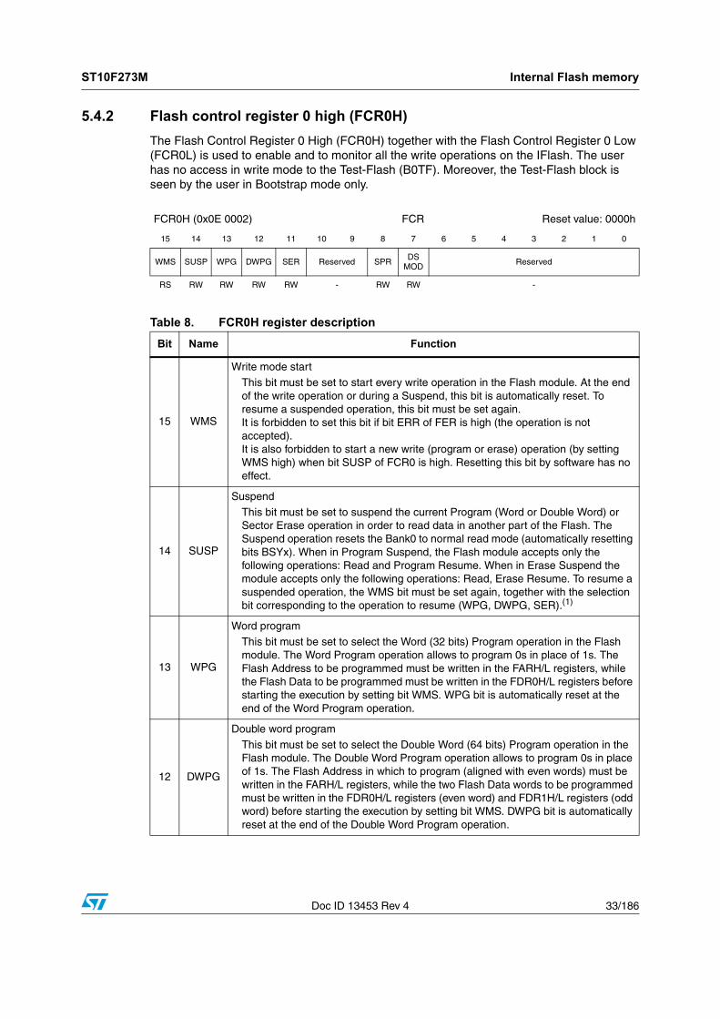
ST10F273M Internal Flash memory
Doc ID 13453 Rev 4 33/186
5.4.2 Flash control register 0 high (FCR0H)
The Flash Control Register 0 High (FCR0H) together with the Flash Control Register 0 Low (FCR0L) is used to enable and to monitor all the write operations on the IFlash. The user has no access in write mode to the Test-Flash (B0TF). Moreover, the Test-Flash block is seen by the user in Bootstrap mode only.
FCR0H (0x0E 0002) FCR Reset value: 0000h
15 14 13 12 11 10 9 8 7 6 5 4 3 2 1 0
WMS SUSP WPG DWPG SER Reserved SPR DSMOD Reserved
RS RW RW RW RW - RW RW -
Table 8. FCR0H register description
Bit Name Function
15 WMS
Write mode start
This bit must be set to start every write operation in the Flash module. At the end of the write operation or during a Suspend, this bit is automatically reset. To resume a suspended operation, this bit must be set again.It is forbidden to set this bit if bit ERR of FER is high (the operation is not accepted).It is also forbidden to start a new write (program or erase) operation (by setting WMS high) when bit SUSP of FCR0 is high. Resetting this bit by software has no effect.
14 SUSP
Suspend
This bit must be set to suspend the current Program (Word or Double Word) or Sector Erase operation in order to read data in another part of the Flash. The Suspend operation resets the Bank0 to normal read mode (automatically resetting bits BSYx). When in Program Suspend, the Flash module accepts only the following operations: Read and Program Resume. When in Erase Suspend the module accepts only the following operations: Read, Erase Resume. To resume a suspended operation, the WMS bit must be set again, together with the selection bit corresponding to the operation to resume (WPG, DWPG, SER).(1)
13 WPG
Word program
This bit must be set to select the Word (32 bits) Program operation in the Flash module. The Word Program operation allows to program 0s in place of 1s. The Flash Address to be programmed must be written in the FARH/L registers, while the Flash Data to be programmed must be written in the FDR0H/L registers before starting the execution by setting bit WMS. WPG bit is automatically reset at the end of the Word Program operation.
12 DWPG
Double word program
This bit must be set to select the Double Word (64 bits) Program operation in the Flash module. The Double Word Program operation allows to program 0s in place of 1s. The Flash Address in which to program (aligned with even words) must be written in the FARH/L registers, while the two Flash Data words to be programmed must be written in the FDR0H/L registers (even word) and FDR1H/L registers (odd word) before starting the execution by setting bit WMS. DWPG bit is automatically reset at the end of the Double Word Program operation.
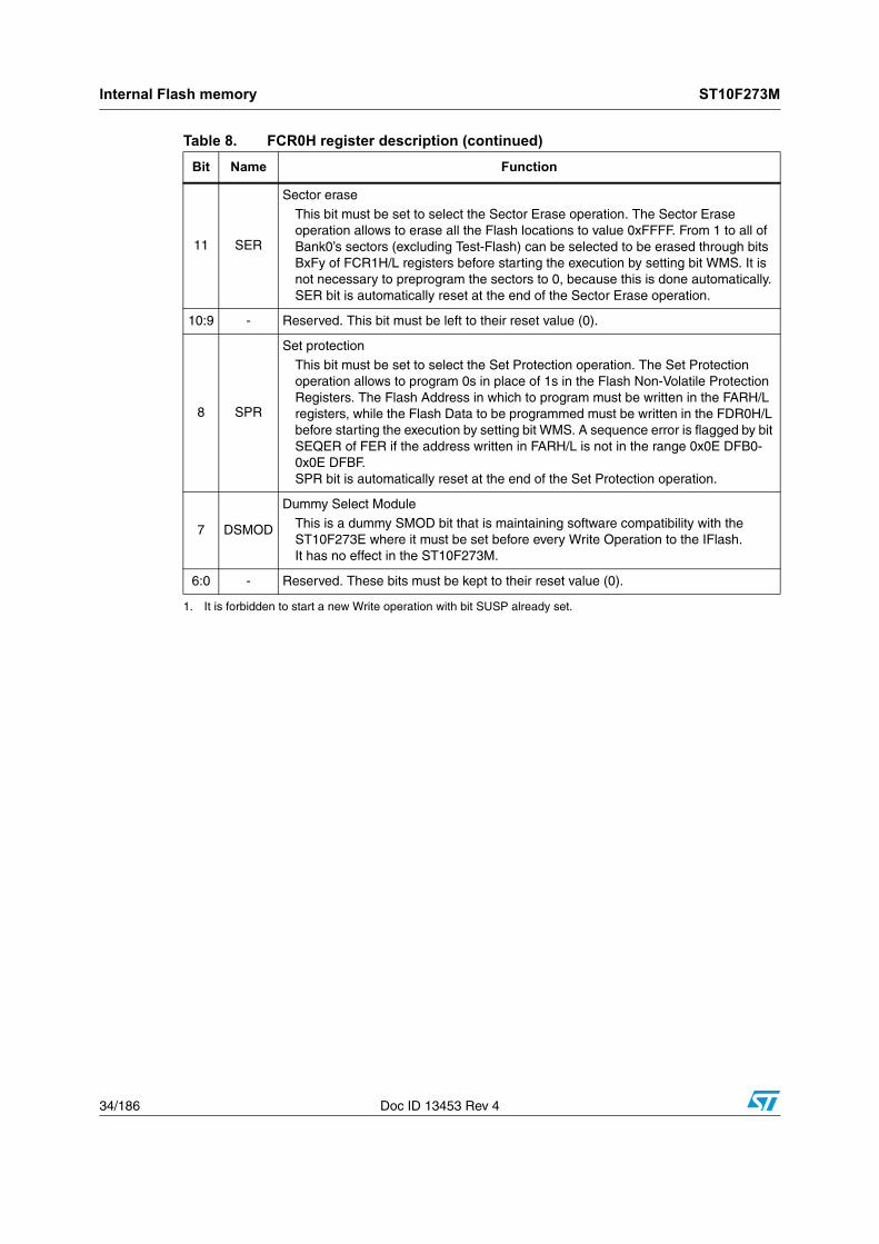
Internal Flash memory ST10F273M
34/186 Doc ID 13453 Rev 4
11 SER
Sector erase
This bit must be set to select the Sector Erase operation. The Sector Erase operation allows to erase all the Flash locations to value 0xFFFF. From 1 to all of Bank0’s sectors (excluding Test-Flash) can be selected to be erased through bits BxFy of FCR1H/L registers before starting the execution by setting bit WMS. It is not necessary to preprogram the sectors to 0, because this is done automatically.SER bit is automatically reset at the end of the Sector Erase operation.
10:9 - Reserved. This bit must be left to their reset value (0).
8 SPR
Set protection
This bit must be set to select the Set Protection operation. The Set Protection operation allows to program 0s in place of 1s in the Flash Non-Volatile Protection Registers. The Flash Address in which to program must be written in the FARH/L registers, while the Flash Data to be programmed must be written in the FDR0H/L before starting the execution by setting bit WMS. A sequence error is flagged by bit SEQER of FER if the address written in FARH/L is not in the range 0x0E DFB0-0x0E DFBF.SPR bit is automatically reset at the end of the Set Protection operation.
7 DSMOD
Dummy Select Module
This is a dummy SMOD bit that is maintaining software compatibility with the ST10F273E where it must be set before every Write Operation to the IFlash.It has no effect in the ST10F273M.
6:0 - Reserved. These bits must be kept to their reset value (0).
1. It is forbidden to start a new Write operation with bit SUSP already set.
Table 8. FCR0H register description (continued)
Bit Name Function
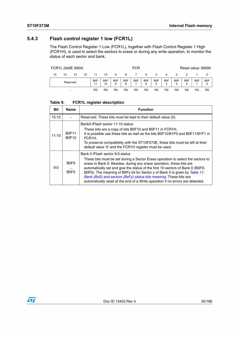
ST10F273M Internal Flash memory
Doc ID 13453 Rev 4 35/186
5.4.3 Flash control register 1 low (FCR1L)
The Flash Control Register 1 Low (FCR1L), together with Flash Control Register 1 High (FCR1H), is used to select the sectors to erase or during any write operation, to monitor the status of each sector and bank.
FCR1L (0x0E 0004) FCR Reset value: 0000h
15 14 13 12 11 10 9 8 7 6 5 4 3 2 1 0
Reserved B0F11
B0F10
B0F9
B0F8
B0F7
B0F6
B0F5
B0F4
B0F3
B0F2
B0F1
B0F0
- RS RS RS RS RS RS RS RS RS RS RS RS
Table 9. FCR1L register description
Bit Name Function
15:12 - Reserved. These bits must be kept to their default value (0).
11:10B0F11B0F10
Bank0 IFlash sector 11:10 status
These bits are a copy of bits B0F10 and B0F11 in FCR1H.It is possible use these bits as well as the bits B0F10/B1F0 and B0F11/B1F1 in FCR1H.To preserve compatibility with the ST10F273E, these bits must be left at their default value ‘0’ and the FCR1H register must be used.
9:0B0F9
...B0F0
Bank 0 IFlash sector 9:0 status
These bits must be set during a Sector Erase operation to select the sectors to erase in Bank 0. Besides, during any erase operation, these bits are automatically set and give the status of the first 10 sectors of Bank 0 (B0F9-B0F0). The meaning of B0Fy bit for Sector y of Bank 0 is given by Table 11: Bank (BxS) and sectors (BxFy) status bits meaning. These bits are automatically reset at the end of a Write operation if no errors are detected.
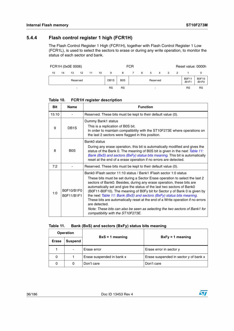
Internal Flash memory ST10F273M
36/186 Doc ID 13453 Rev 4
5.4.4 Flash control register 1 high (FCR1H)
The Flash Control Register 1 High (FCR1H), together with Flash Control Register 1 Low (FCR1L), is used to select the sectors to erase or during any write operation, to monitor the status of each sector and bank.
FCR1H (0x0E 0006) FCR Reset value: 0000h
15 14 13 12 11 10 9 8 7 6 5 4 3 2 1 0
Reserved DB1S B0S Reserved B0F11/B1F1
B0F10/B1F0
- RS RS - RS RS
Table 10. FCR1H register description
Bit Name Function
15:10 - Reserved. These bits must be kept to their default value (0).
9 DB1S
Dummy Bank1 status
This is a replication of B0S bit.In order to maintain compatibility with the ST10F273E where operations on the last 2 sectors were flagged in this position.
8 B0S
Bank0 statusDuring any erase operation, this bit is automatically modified and gives the status of the Bank 0. The meaning of B0S bit is given in the next Table 11: Bank (BxS) and sectors (BxFy) status bits meaning. This bit is automatically reset at the end of a erase operation if no errors are detected.
7:2 - Reserved. These bits must be kept to their default value (0).
1:0B0F10/B1F0B0F11/B1F1
Bank0 IFlash sector 11:10 status / Bank1 IFlash sector 1:0 status
These bits must be set during a Sector Erase operation to select the last 2 sectors of Bank0. Besides, during any erase operation, these bits are automatically set and give the status of the last two sectors of Bank0 (B0F11-B0F10). The meaning of B0Fy bit for Sector y of Bank 0 is given by the next Table 11: Bank (BxS) and sectors (BxFy) status bits meaning. These bits are automatically reset at the end of a Write operation if no errors are detected.Note: These bits can also be seen as selecting the two sectors of Bank1 for compatibility with the ST10F273E.
Table 11. Bank (BxS) and sectors (BxFy) status bits meaning
OperationBxS = 1 meaning BxFy = 1 meaning
Erase Suspend
1 - Erase error Erase error in sector y
0 1 Erase suspended in bank x Erase suspended in sector y of bank x
0 0 Don’t care Don’t care
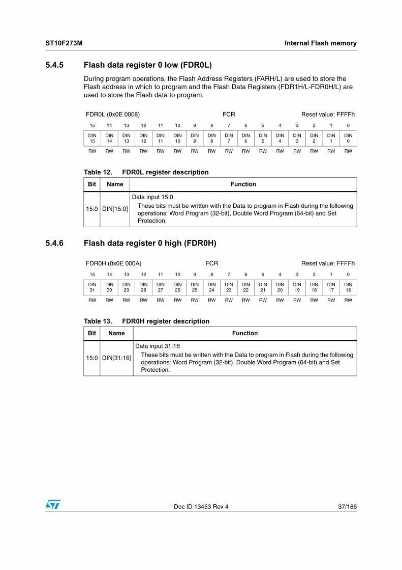
ST10F273M Internal Flash memory
Doc ID 13453 Rev 4 37/186
5.4.5 Flash data register 0 low (FDR0L)
During program operations, the Flash Address Registers (FARH/L) are used to store the Flash address in which to program and the Flash Data Registers (FDR1H/L-FDR0H/L) are used to store the Flash data to program.
5.4.6 Flash data register 0 high (FDR0H)
FDR0L (0x0E 0008) FCR Reset value: FFFFh
15 14 13 12 11 10 9 8 7 6 5 4 3 2 1 0
DIN15
DIN14
DIN13
DIN12
DIN11
DIN10
DIN9
DIN8
DIN7
DIN6
DIN5
DIN4
DIN3
DIN2
DIN1
DIN0
RW RW RW RW RW RW RW RW RW RW RW RW RW RW RW RW
Table 12. FDR0L register description
Bit Name Function
15:0 DIN[15:0]
Data input 15:0
These bits must be written with the Data to program in Flash during the following operations: Word Program (32-bit), Double Word Program (64-bit) and Set Protection.
FDR0H (0x0E 000A) FCR Reset value: FFFFh
15 14 13 12 11 10 9 8 7 6 5 4 3 2 1 0
DIN31
DIN30
DIN29
DIN28
DIN27
DIN26
DIN25
DIN24
DIN23
DIN22
DIN21
DIN20
DIN19
DIN18
DIN17
DIN16
RW RW RW RW RW RW RW RW RW RW RW RW RW RW RW RW
Table 13. FDR0H register description
Bit Name Function
15:0 DIN[31:16]
Data input 31:16
These bits must be written with the Data to program in Flash during the following operations: Word Program (32-bit), Double Word Program (64-bit) and Set Protection.

Internal Flash memory ST10F273M
38/186 Doc ID 13453 Rev 4
5.4.7 Flash data register 1 low (FDR1L)
5.4.8 Flash data register 1 high (FDR1H)
5.4.9 Flash address register low (FARL)
FDR1L (0x0E 000C) FCR Reset value: FFFFh
15 14 13 12 11 10 9 8 7 6 5 4 3 2 1 0
DIN15 DIN14 DIN13 DIN12 DIN11 DIN10 DIN9 DIN8 DIN7 DIN6 DIN5 DIN4 DIN3 DIN2 DIN1 DIN0
RW RW RW RW RW RW RW RW RW RW RW RW RW RW RW RW
Table 14. FDR1L register description
Bit Name Function
15:0 DIN[15:0]Data input 15:0
These bits must be written with the Data to program in Flash during the following operations: Double Word Program (64-bit) and Set Protection.
FDR1H (0x0E 000E) FCR Reset value: FFFFh
15 14 13 12 11 10 9 8 7 6 5 4 3 2 1 0
DIN31 DIN30 DIN29 DIN28 DIN27 DIN26 DIN25 DIN24 DIN23 DIN22 DIN21 DIN20 DIN19 DIN18 DIN17 DIN16
RW RW RW RW RW RW RW RW RW RW RW RW RW RW RW RW
Table 15. FDR1H register description
Bit Name Function
15:0 DIN[31:16]Data input 31:16
These bits must be written with the Data to program in Flash during the following operations: Double Word Program (64-bit) and Set Protection.
FARL (0x0E 0010) FCR Reset value: 0000h
15 14 13 12 11 10 9 8 7 6 5 4 3 2 1 0
ADD15 ADD14 ADD13 ADD12 ADD11 ADD10 ADD9 ADD8 ADD7 ADD6 ADD5 ADD4 ADD3 ADD2 Reserved
RW RW RW RW RW RW RW RW RW RW RW RW RW RW -
Table 16. FARL register description
Bit Name Function
15:2 ADD[15:2]
Address 15:2
These bits must be written with the Address of the Flash location to program during the following operations: Word Program (32-bit) and Double Word Program (64-bit).In Double Word Program bit ADD2 must be written to ‘0’.
1:0 - Reserved. These bits must be kept to their default value (0).
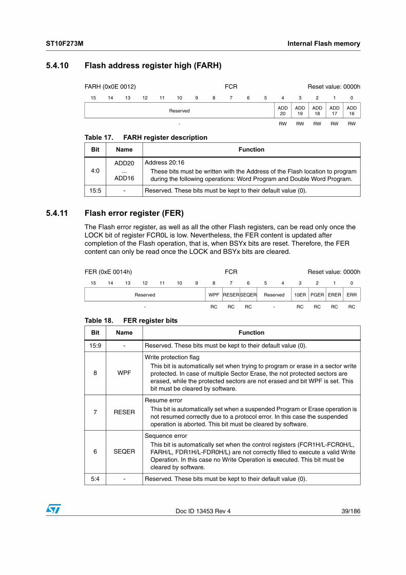
ST10F273M Internal Flash memory
Doc ID 13453 Rev 4 39/186
5.4.10 Flash address register high (FARH)
5.4.11 Flash error register (FER)
The Flash error register, as well as all the other Flash registers, can be read only once the LOCK bit of register FCR0L is low. Nevertheless, the FER content is updated after completion of the Flash operation, that is, when BSYx bits are reset. Therefore, the FER content can only be read once the LOCK and BSYx bits are cleared.
FARH (0x0E 0012) FCR Reset value: 0000h
15 14 13 12 11 10 9 8 7 6 5 4 3 2 1 0
Reserved ADD20
ADD19
ADD18
ADD17
ADD16
- RW RW RW RW RW
Table 17. FARH register description
Bit Name Function
4:0ADD20
...ADD16
Address 20:16
These bits must be written with the Address of the Flash location to program during the following operations: Word Program and Double Word Program.
15:5 - Reserved. These bits must be kept to their default value (0).
FER (0xE 0014h) FCR Reset value: 0000h
15 14 13 12 11 10 9 8 7 6 5 4 3 2 1 0
Reserved WPF RESER SEQER Reserved 10ER PGER ERER ERR
- RC RC RC - RC RC RC RC
Table 18. FER register bits
Bit Name Function
15:9 - Reserved. These bits must be kept to their default value (0).
8 WPF
Write protection flagThis bit is automatically set when trying to program or erase in a sector write protected. In case of multiple Sector Erase, the not protected sectors are erased, while the protected sectors are not erased and bit WPF is set. This bit must be cleared by software.
7 RESER
Resume errorThis bit is automatically set when a suspended Program or Erase operation is not resumed correctly due to a protocol error. In this case the suspended operation is aborted. This bit must be cleared by software.
6 SEQER
Sequence error
This bit is automatically set when the control registers (FCR1H/L-FCR0H/L, FARH/L, FDR1H/L-FDR0H/L) are not correctly filled to execute a valid Write Operation. In this case no Write Operation is executed. This bit must be cleared by software.
5:4 - Reserved. These bits must be kept to their default value (0).

Internal Flash memory ST10F273M
40/186 Doc ID 13453 Rev 4
5.4.12 XFlash interface control dummy register (XFICR)
5.5 Protection strategy
The protection bits are stored in Non-Volatile Flash cells that are read once at reset and stored in five Volatile registers. Before they are read from the Non-Volatile cells, all the available protections are forced active during reset.
3 10ER
1 over 0 error
This bit is automatically set when trying to program at 1 bits previously set at 0 (this does not happen when programming the Protection bits). This error is not due to a failure of the Flash cell, but only flags that the desired data has not been written. This bit must be cleared by software.
2 PGER
Program error
This bit is automatically set when a Program error occurs during a Flash write operation. This error is due to a real failure of a Flash cell, that can no more be programmed. The word where this error occurred must be discarded. This bit must be cleared by software.
1 ERER
Erase error
This bit is automatically set when an Erase error occurs during a Flash write operation. This error is due to a real failure of a Flash cell, that can no more be erased. This kind of error is fatal and the sector where it occurred must be discarded. This bit must be cleared by software.
0 ERR
Write errorThis bit is automatically set when an error occurs during a Flash write operation or when a bad write operation setup is done. Once the error has been discovered and understood, ERR bit must be cleared by software.
Table 18. FER register bits (continued)
Bit Name Function
XFICR (0x0E E0000) FCR Reset value: 0007h
15 14 13 12 11 10 9 8 7 6 5 4 3 2 1 0
Reserved WS3 WS2 WS1 WS0
- RW RW RW RW
Table 19. XFlash interface control register
Bit Name Function
3:0 WS3...WS0
Dummy Wait States 3:0
In the ST10F273E, these bits were used to configure the number of wait-states to access the XFlash. As there is no XFlash on the Root part number 1, these bits have no effect.This register is implemented for software compatibility with the ST10F273E.
15:4 - Reserved. These bits must be kept to their default value (0).

ST10F273M Internal Flash memory
Doc ID 13453 Rev 4 41/186
Note: The protection bits in the Non-Volatile registers are programmable one time and this programing is permanent. Temporary unprotection will be handled with their Volatile equivalent.
The protections can be programmed using the Set Protection operation (see Section 5.4: Flash control registers description) that must be executed from the on-chip RAMs or from external memories.
Two kind of protections are available:
● write protections to avoid unwanted writings
● access protections to avoid piracy
The next sections show the different level of protections and highlight the architecture limitations.
5.5.1 Protection registers
The five Non-Volatile Protection Registers are one-time programmable for the user.
Two registers, FVWPIRL and FVWPIRH, are used to store the Write Protection fuses for each sector IFlash module. The other three registers (FNVAPR0 and FNVAPR1L/H) are used to store the Access Protection fuses.
Note: On-going protection operations are flagged with BSYNVR, bit 1 of FCR0L register.
5.5.2 Flash non-volatile write protection I register low (FNVWPIRL)
FNVWPIRL (0x0E DFB4) NVR Delivery value: FFFFh
15 14 13 12 11 10 9 8 7 6 5 4 3 2 1 0
Reserved W0P11
W0P10
W0P9
W0P8
W0P7
W0P6
W0P5
W0P4
W0P3
W0P2
W0P1
W0P0
- RO RO RW RW RW RW RW RW RW RW RW RW
Table 20. FNVWPIRL register bits
Bit Name Function
15:12 -Reserved. These bits must be left to their default value ‘1’ when programming PVWPIRL.
11:10W0P11W0P10
Read-Only for Write protection Bank0 sectors 11 and 10These bits must be left to their default value ‘1’ when programming FVWPIRL (they can not be used to set write protection on sectors B0F11 and B0F10).After a protection command, these bits will reflect the value of bit 0 and 1 of FVWPIRH register (W0P11 and W0P10).
9:0W0P9
...W0P0
Write protection bank 0 / sectors 9-0These bits, if programmed at 0, disable any write access to the sectors of Bank 0 (IFlash).

Internal Flash memory ST10F273M
42/186 Doc ID 13453 Rev 4
5.5.3 Flash non-volatile write protection I register high (FNVWPIRH)
5.5.4 Flash non-volatile write protection I register low Mirror (FNVWPIRL-m)
This register is mirroring the register at FVWPIRL (address 0x0E DFB4). It is intended to maintain software compatibility with the ST10F273E.
In applications ported from a ST10F273E, FVWPIRL-m register (address 0x0E DFB0) must be used to maintain the existing Flash drivers.
In applications ported from a ST10F272x, FVWPIRL register (address 0x0E DFB4) must be used to maintain existing drivers.
5.5.5 Flash non-volatile write protection I register high Mirror (FVWPIRH-m)
This register is mirroring the register at FVWPIRH (address 0x0E DFB6). It is intended to maintain software compatibility with the ST10F273E.
In applications ported from a ST10F273E, FVWPIRH-m register (address 0x0E DFB2) must be used to maintain the existing Flash drivers.
In applications ported from a ST10F272x, FVWPIRH register (address 0x0E DFB6) must be used to maintain existing drivers.
FNVWPIRH (0x0E DFB6) NVR Delivery value: FFFFh
15 14 13 12 11 10 9 8 7 6 5 4 3 2 1 0
Reserved W0P11-W1P1
W0P10-W1P0
- RW RW
Table 21. FNVWPRIH register bits
Bit Name Function
15:2 - Reserved. These bits must be left to their default value ‘1’.
1:0W0P11/W1P1W0P10/W1P0
Write protection Bank0 - sectors 11:10 / Write protection Bank1 - sectors 1:0
These bits, if programmed at 0, disable any write access to the selected sectors.
FNVWPIRL-m (0x0E DFB0) NVR Delivery value: FFFFh
15 14 13 12 11 10 9 8 7 6 5 4 3 2 1 0
Reserved W0P11
W0P10
W0P9
W0P8
W0P7
W0P6
W0P5
W0P4
W0P3
W0P2
W0P1
W0P0
- RO RO RW RW RW RW RW RW RW RW RW RW
FVWPIRH-m (0x0E DFB2 NVR Delivery value: FFFFh
15 14 13 12 11 10 9 8 7 6 5 4 3 2 1 0
Reserved W0P11-W1P1
W0P10-W1P0
- RW RW

ST10F273M Internal Flash memory
Doc ID 13453 Rev 4 43/186
5.5.6 Flash non-volatile access protection register 0 (FNVAPR0)
5.5.7 Flash non-volatile access protection register 1 low (FNVAPR1L)
FNVAPR0 (0x0E DFB8) NVR Delivery value: ACFFh
15 14 13 12 11 10 9 8 7 6 5 4 3 2 1 0
Reserved DBGP ACCP
- RW RW
Table 22. FNVAPR0 register bits
Bit Name Description
15:2 - Reserved. These bits must be left to their default value.
1 DBGP
Debug protection
This bit, if erased at 1, allows to bypass all the protections using the Debug features through the Test Interface. If programmed at 0, on the contrary, all the debug features, the Test Interface and all the Flash Test modes are disabled.Even STMicroelectronics will not be able to access the device to run any eventual failure analysis.
0 ACCP
Access protection
This bit, if programmed at 0, disables any access (read/write) to data mapped inside IFlash Module address space, unless the current instruction is fetched from IFlash.
FNVAPR1L (0x0E DFBC) NVR Delivery value: FFFFh
15 14 13 12 11 10 9 8 7 6 5 4 3 2 1 0
PDS15 PDS14 PDS13 PDS12 PDS11 PDS10 PDS9 PDS8 PDS7 PDS6 PDS5 PDS4 PDS3 PDS2 PDS1 PDS0
RW RW RW RW RW RW RW RW RW RW RW RW RW RW RW RW
Table 23. FNVAPR1L register bits
Bit Name Function
15:0PDS15
...PDS0
Protections disable15-0If bit PDSx is programmed at 0 and bit PENx is erased at 1, the action of bit ACCP is disabled. Bit PDS0 can be programmed at 0 only if both bits DBGP and ACCP have already been programmed at 0. Bit PDSx can be programmed at 0 only if bit PENx-1 has already been programmed at 0.
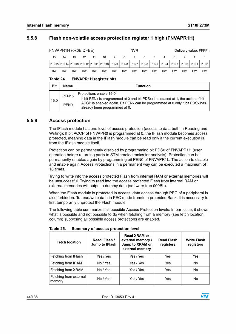
Internal Flash memory ST10F273M
44/186 Doc ID 13453 Rev 4
5.5.8 Flash non-volatile access protection register 1 high (FNVAPR1H)
5.5.9 Access protection
The IFlash module has one level of access protection (access to data both in Reading and Writing): If bit ACCP of FNVAPR0 is programmed at 0, the IFlash module becomes access protected, meaning data in the IFlash module can be read only if the current execution is from the IFlash module itself.
Protection can be permanently disabled by programming bit PDS0 of FNVAPR1H (user operation before returning parts to STMicroelectronics for analysis). Protection can be permanently enabled again by programming bit PEN0 of FNVAPR1L. The action to disable and enable again Access Protections in a permanent way can be executed a maximum of 16 times.
Trying to write into the access protected Flash from internal RAM or external memories will be unsuccessful. Trying to read into the access protected Flash from internal RAM or external memories will output a dummy data (software trap 009Bh).
When the Flash module is protected in access, data access through PEC of a peripheral is also forbidden. To read/write data in PEC mode from/to a protected Bank, it is necessary to first temporarily unprotect the Flash module.
The following table summarizes all possible Access Protection levels: In particular, it shows what is possible and not possible to do when fetching from a memory (see fetch location column) supposing all possible access protections are enabled.
FNVAPR1H (0x0E DFBE) NVR Delivery value: FFFFh
15 14 13 12 11 10 9 8 7 6 5 4 3 2 1 0
PEN15 PEN14 PEN13 PEN12 PEN11 PEN10 PEN9 PEN8 PEN7 PEN6 PEN5 PEN4 PEN3 PEN2 PEN1 PEN0
RW RW RW RW RW RW RW RW RW RW RW RW RW RW RW RW
Table 24. FNVAPR1H register bits
Bit Name Function
15:0PEN15
...PEN0
Protections enable 15-0
If bit PENx is programmed at 0 and bit PDSx+1 is erased at 1, the action of bit ACCP is enabled again. Bit PENx can be programmed at 0 only if bit PDSx has already been programmed at 0.
Table 25. Summary of access protection level
Fetch locationRead IFlash /
Jump to IFlash
Read XRAM or external memory /Jump to XRAM or external memory
Read Flash registers
Write Flash registers
Fetching from IFlash Yes / Yes Yes / Yes Yes Yes
Fetching from IRAM No / Yes Yes / Yes Yes No
Fetching from XRAM No / Yes Yes / Yes Yes No
Fetching from external memory
No / Yes Yes / Yes Yes No
ST10F273M Internal Flash memory
Doc ID 13453 Rev 4 45/186
5.5.10 Write protection
The Flash modules have one level of Write Protections: Each sector can be Software Write Protected by programming at 0 the related bit WyPx in FNVWPIRL/H register.
5.5.11 Temporary unprotection
Bits WyPx of FNVWPIRL/H can be temporarily unprotected by executing the Set Protection operation and writing 1 into these bits.
Bit ACCP can be temporarily unprotected by executing the Set Protection operation and writing are executed from IFlash.
To restore the write access protection bits it is necessary to reset the microcontroller or to execute a Set Protection operation and write 0 into the desired bits.
In reality, when a temporary unprotection operation is executed, the corresponding volatile register is written to 1, while the non-volatile registers bits previously written to 0 (for a protection set operation), will continue to maintain the 0. For this reason, the user software must be in charge to track the current protection status (for instance using a specific RAM area), it is not possible to deduce it by reading the non-volatile register content (a temporary unprotection cannot be detected).
5.6 Write operation examples
In the following, examples for each kind of Flash write operation are presented.
The examples are showing the sequence of instructions needed to start an operation. Write operations should be followed by a status check (FER register).
Note: After a write operation has started, the Flash control registers are not accessible for a short time. The LOCK bit, bit 4 of FCR0L register, must be polled in order to know when the Flash control registers can be accessed again (LOCK = ‘1’: no access to Flash control registers).
Write operation on IBus registers is 16 bits wide.
Word program
Example: 32-bit Word Program of data 0xAAAAAAAA at address 0x025554FCR0H|= 0x2000; /*Set WPG in FCR0H*/
FARL = 0x5554; /*Load Add in FARL*/
FARH = 0x0002; /*Load Add in FARH*/
FDR0L = 0xAAAA; /*Load Data in FDR0L*/
FDR0H = 0xAAAA; /*Load Data in FDR0H*/
FCR0H|= 0x8000; /*Operation start*/
Double word program
Example: Double Word Program (64-bit) of data 0x55AA55AA at address 0x035558 and data 0xAA55AA55 at address 0x03555C.
FCR0H |= 0x1000; /*Set DWPG in FCR0H*/
FARL = 0x5558; /*Load Add in FARL*/
FARH = 0x0003; /*Load Add in FARH*/
FDR0L = 0x55AA; /*Load Data in FDR0L*/
Internal Flash memory ST10F273M
46/186 Doc ID 13453 Rev 4
FDR0H = 0x55AA; /*Load Data in FDR0H*/
FDR1L = 0xAA55; /*Load Data in FDR1L*/
FDR1H = 0xAA55; /*Load Data in FDR1H*/
FCR0H |= 0x8000; /*Operation start*/
Double Word Program is always performed on the Double Word aligned on an even Word: bit ADD2 of FARL is ignored.
Sector erase
Example: Sector Erase of sectors B0F1 and B0F0 of Bank 0.FCR0H |= 0x0800; /*Set SER in FCR0H*/
FCR1L |= 0x0003; /*Set B0F1, B0F0*/
FCR0H |= 0x8000; /*Operation start*/
Suspend and resume
Word Program, Double Word Program, and Sector Erase operations can be suspended in the following way:
FCR0H |= 0x4000; /*Set SUSP in FCR0H*/
Then the operation can be resumed in the following way:FCR0H |= 0x0800; /*Set SER in FCR0H*/
FCR0H |= 0x8000; /*Operation resume*/
Before resuming a suspended Erase, FCR1H/FCR1L must be read to check if the Erase is already completed (FCR1H = FCR1L = 0x0000 if Erase is complete). Original setup of Select Operation bits in FCR0H/L must be restored before the operation resume, otherwise the operation is aborted and bit RESER of FER is set.
Set protection
Example 1: Enable Write Protection of sectors B0F3-0 of Bank 0.FCR0H |= 0x0100; /*Set SPR in FCR0H*/
FARL = 0xDFB4; /*Load Add of register FNVWPIR in FARL*/
FARH = 0x000E; /*Load Add of register FNVWPIR in FARH*/
FDR0L = 0xFFF0; /*Load Data in FDR0L*/
FDR0H = 0xFFFF; /*Load Data in FDR0H*/
FCR0H |= 0x8000; /*Operation start*/
Example 2: Enable Access and Debug Protection.FCR0H |= 0x0100; /*Set SPR in FCR0H*/
FARL = 0xDFB8; /*Load Add of register FNVAPR0 in FARL*/
FARH = 0x000E; /*Load Add of register FNVAPR0 in FARH*/
FDR0L = 0xFFFC; /*Load Data in FDR0L*/
FCR0H |= 0x8000; /*Operation start*/
Example 3: Disable in a permanent way Access and Debug Protection.FCR0H |= 0x0100; /*Set SPR in FCR0H*/
FCR0H |= 0x0100; /*Set SPR in FCR0H*/
FARL = 0xDFBC; /*Load Add of register FNVAPR1L in FARL*/
FARH = 0x000E; /*Load Add of register FNVAPR1L in FARH*/
ST10F273M Internal Flash memory
Doc ID 13453 Rev 4 47/186
FDR0L = 0xFFFE; /*Load Data in FDR0L for clearing PDS0*/
FCR0H |= 0x8000; /*Operation start*/
Example 4: Enable again in a permanent way Access and Debug Protection, after having disabled them.
FCR0H|= 0x0100; /*Set SPR in FCR0H*/
FARL = 0xDFBC; /*Load Add register FNVAPR1H in FARL*/
FARH = 0x000E; /*Load Add register FNVAPR1H in FARH*/
FDR0H = 0xFFFE; /*Load Data in FDR0H to clear PEN0*/
FCR0H|= 0x8000; /*Operation start*/
Disable and re-enable of Access and Debug Protection in a permanent way (as shown by examples 3 and 4) can be done for a maximum of 16 times.

Internal Flash memory ST10F273M
48/186 Doc ID 13453 Rev 4
5.7 Write operation summary
In general, each write operation is started through a sequence of three steps:
1. The first instruction is used to select the desired operation by setting its corresponding selection bit in the Flash Control Register 0.
2. The second step is the definition of the Address and Data for programming or the sectors to erase.
3. The last instruction is used to start the write operation, by setting the start bit WMS in the FCR0. This last instruction must not be executed from Flash.
Once selected, but not yet started, one operation can be canceled by resetting the operation selection bit.
Available Flash Module Write Operations are summarized in the following Table 26.
Figure 7 shows the complete flow needed for a Write operation.
Figure 7. Write operation control flow
Table 26. Flash write operations
Operation Select bit Address and data Start bit
Word program (32-bit) WPGFARL/FARH
FDR0L/FDR0H
WMSDouble word program (64-bit) DWPGFARL/FARH
FDR0L/FDR0HFDR1L/FDR1H
Sector erase SER FCR1L/FCR1H
Set protection SPR FDR0L/FDR0H
Program/erase suspend SUSP None None

ST10F273M Bootstrap loader
Doc ID 13453 Rev 4 49/186
6 Bootstrap loader
The ST10F273M implements Boot capabilities in order to:
● Support bootstrap via UART or bootstrap via CAN for the standard bootstrap
● Support a Selective Bootstrap Loader, to manage the bootstrap sequence in a different way
6.1 Selection among user-code, standard or selective bootstrap
The boot modes are triggered with a special combination set on Port0L[5...4]. Those signals, as other configuration signals, are latched on the rising edge of RSTIN pin.
● Decoding of reset configuration (P0L.5 = 1, P0L.4 = 1) selects the normal mode (also called User mode) and selects the user Flash to be mapped from address 00’0000h.
● Decoding of reset configuration (P0L.5 = 1, P0L.4 = 0) selects ST10 standard bootstrap mode (Test-Flash is active and overlaps user Flash for code fetches from address 00'0000h; user Flash is active and available for read accesses).
● Decoding of reset configuration (P0L.5 = 0, P0L.4 = 1) activates additional verifications to select which bootstrap software to execute:
– if the User mode signature in the User Flash is programmed correctly, then a software reset sequence is selected and the User code is executed;
– if the User mode signature is not programmed correctly in the user Flash, then the User key location is read again. Its value determines which communication channel will be enabled for bootstrapping.
.
6.2 Standard bootstrap loader
After entering the standard BSL mode and the respective initialization, the ST10F273M scans the RxD0 line and the CAN1_RxD line to receive either a valid dominant bit from the CAN interface or a start condition from the UART line.
Start condition on UART RxD: ST10F273M starts standard bootstrap loader. This bootstrap loader is identical to that of other ST10 devices (example: ST10F269, ST10F168).
Valid dominant bit on CAN1 RxD: ST10F273M start bootstrapping via CAN1.
Caution: As both UART_RxD and CAN1_RxD lines are polled to detect a start of communication, ensure a stable level on the unused channel by adding a pull-up resistor.
Table 27. ST10F273M boot mode selection
P0.5 P0.4 ST10 decoding
1 1 User mode: User Flash mapped at 00’0000h
1 0Standard Bootstrap Loader: User Flash mapped from 00’0000h, code fetches redirected to Test-Flash at 00’0000h
0 1Selective Boot mode: User Flash mapped from 00’0000h, code fetches redirected to Test-Flash at 00’0000h (different sequence execution compared to Standard Bootstrap Loader)
0 0 Reserved

Bootstrap loader ST10F273M
50/186 Doc ID 13453 Rev 4
6.3 Alternate and selective boot mode (ABM and SBM)
6.3.1 Activation of the ABM and SBM
Alternate boot is activated with the combination ‘01’ on Port0L[5..4] at the rising edge of RSTIN.
6.3.2 User mode signature integrity check
The behavior of the Selective Boot mode is based on the computing of a signature between the content of two memory locations and a comparison with a reference signature. This requires that users who use Selective Boot have reserved and programmed the Flash memory locations.
6.3.3 Selective boot mode
When the user signature is not correct, instead of executing the Standard Bootstrap Loader (triggered by P0L.4 low at reset), additional check is made.
Depending on the value at the User key location, the following behavior occurs:
● A jump is performed to the Standard Bootstrap Loader
● Only UART is enabled for bootstrapping
● Only CAN1 is enabled for bootstrapping
● The device enters an infinite loop
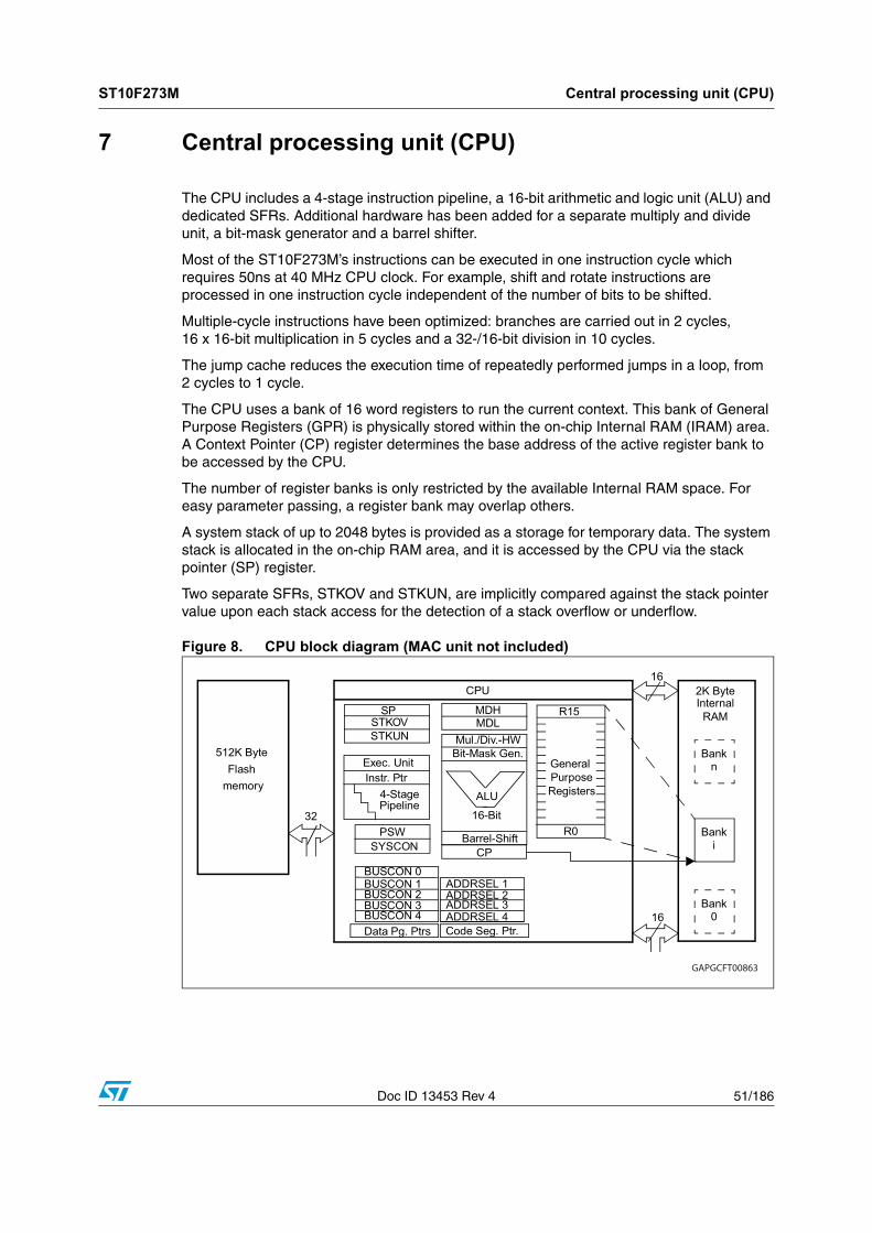
ST10F273M Central processing unit (CPU)
Doc ID 13453 Rev 4 51/186
7 Central processing unit (CPU)
The CPU includes a 4-stage instruction pipeline, a 16-bit arithmetic and logic unit (ALU) and dedicated SFRs. Additional hardware has been added for a separate multiply and divide unit, a bit-mask generator and a barrel shifter.
Most of the ST10F273M’s instructions can be executed in one instruction cycle which requires 50ns at 40 MHz CPU clock. For example, shift and rotate instructions are processed in one instruction cycle independent of the number of bits to be shifted.
Multiple-cycle instructions have been optimized: branches are carried out in 2 cycles, 16 x 16-bit multiplication in 5 cycles and a 32-/16-bit division in 10 cycles.
The jump cache reduces the execution time of repeatedly performed jumps in a loop, from 2 cycles to 1 cycle.
The CPU uses a bank of 16 word registers to run the current context. This bank of General Purpose Registers (GPR) is physically stored within the on-chip Internal RAM (IRAM) area. A Context Pointer (CP) register determines the base address of the active register bank to be accessed by the CPU.
The number of register banks is only restricted by the available Internal RAM space. For easy parameter passing, a register bank may overlap others.
A system stack of up to 2048 bytes is provided as a storage for temporary data. The system stack is allocated in the on-chip RAM area, and it is accessed by the CPU via the stack pointer (SP) register.
Two separate SFRs, STKOV and STKUN, are implicitly compared against the stack pointer value upon each stack access for the detection of a stack overflow or underflow.
Figure 8. CPU block diagram (MAC unit not included)
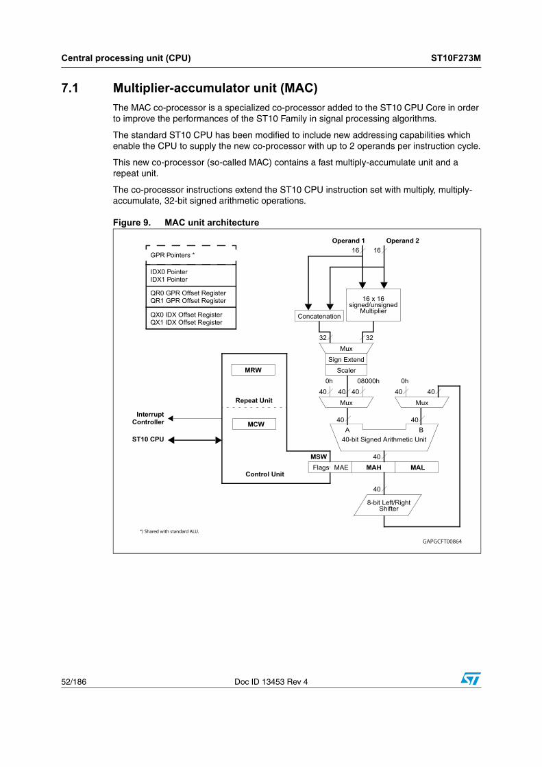
Central processing unit (CPU) ST10F273M
52/186 Doc ID 13453 Rev 4
7.1 Multiplier-accumulator unit (MAC)
The MAC co-processor is a specialized co-processor added to the ST10 CPU Core in order to improve the performances of the ST10 Family in signal processing algorithms.
The standard ST10 CPU has been modified to include new addressing capabilities which enable the CPU to supply the new co-processor with up to 2 operands per instruction cycle.
This new co-processor (so-called MAC) contains a fast multiply-accumulate unit and a repeat unit.
The co-processor instructions extend the ST10 CPU instruction set with multiply, multiply-accumulate, 32-bit signed arithmetic operations.
Figure 9. MAC unit architecture
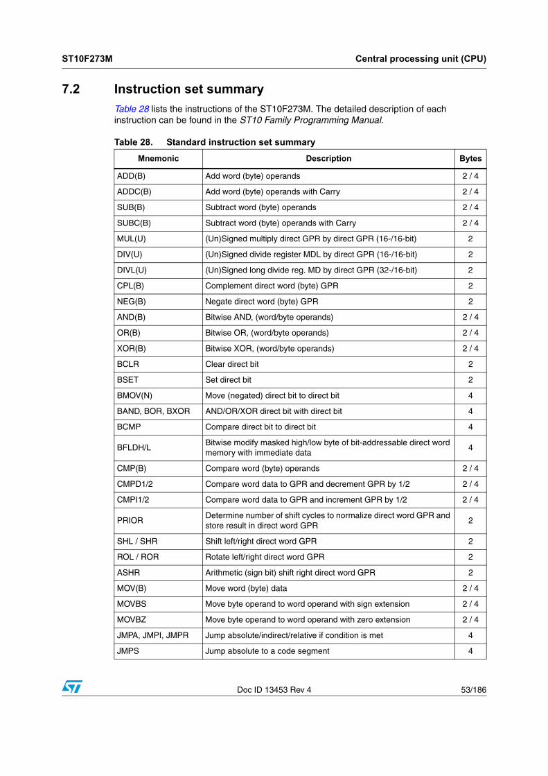
ST10F273M Central processing unit (CPU)
Doc ID 13453 Rev 4 53/186
7.2 Instruction set summary
Table 28 lists the instructions of the ST10F273M. The detailed description of each instruction can be found in the ST10 Family Programming Manual.
Table 28. Standard instruction set summary
Mnemonic Description Bytes
ADD(B) Add word (byte) operands 2 / 4
ADDC(B) Add word (byte) operands with Carry 2 / 4
SUB(B) Subtract word (byte) operands 2 / 4
SUBC(B) Subtract word (byte) operands with Carry 2 / 4
MUL(U) (Un)Signed multiply direct GPR by direct GPR (16-/16-bit) 2
DIV(U) (Un)Signed divide register MDL by direct GPR (16-/16-bit) 2
DIVL(U) (Un)Signed long divide reg. MD by direct GPR (32-/16-bit) 2
CPL(B) Complement direct word (byte) GPR 2
NEG(B) Negate direct word (byte) GPR 2
AND(B) Bitwise AND, (word/byte operands) 2 / 4
OR(B) Bitwise OR, (word/byte operands) 2 / 4
XOR(B) Bitwise XOR, (word/byte operands) 2 / 4
BCLR Clear direct bit 2
BSET Set direct bit 2
BMOV(N) Move (negated) direct bit to direct bit 4
BAND, BOR, BXOR AND/OR/XOR direct bit with direct bit 4
BCMP Compare direct bit to direct bit 4
BFLDH/LBitwise modify masked high/low byte of bit-addressable direct word memory with immediate data
4
CMP(B) Compare word (byte) operands 2 / 4
CMPD1/2 Compare word data to GPR and decrement GPR by 1/2 2 / 4
CMPI1/2 Compare word data to GPR and increment GPR by 1/2 2 / 4
PRIORDetermine number of shift cycles to normalize direct word GPR and store result in direct word GPR
2
SHL / SHR Shift left/right direct word GPR 2
ROL / ROR Rotate left/right direct word GPR 2
ASHR Arithmetic (sign bit) shift right direct word GPR 2
MOV(B) Move word (byte) data 2 / 4
MOVBS Move byte operand to word operand with sign extension 2 / 4
MOVBZ Move byte operand to word operand with zero extension 2 / 4
JMPA, JMPI, JMPR Jump absolute/indirect/relative if condition is met 4
JMPS Jump absolute to a code segment 4

Central processing unit (CPU) ST10F273M
54/186 Doc ID 13453 Rev 4
J(N)B Jump relative if direct bit is (not) set 4
JBC Jump relative and clear bit if direct bit is set 4
JNBS Jump relative and set bit if direct bit is not set 4
CALLA, CALLI, CALLR
Call absolute/indirect/relative subroutine if condition is met 4
CALLS Call absolute subroutine in any code segment 4
PCALLPush direct word register onto system stack and call absolute subroutine
4
TRAP Call interrupt service routine via immediate trap number 2
PUSH, POP Push/pop direct word register onto/from system stack 2
SCXTPush direct word register onto system stack and update register with word operand
4
RET Return from intra-segment subroutine 2
RETS Return from inter-segment subroutine 2
RETPReturn from intra-segment subroutine and pop direct word register from system stack
2
RETI Return from interrupt service subroutine 2
SRST Software Reset 4
IDLE Enter Idle mode 4
PWRDN Enter Power-down mode (supposes NMI-pin being low) 4
SRVWDT Service Watchdog Timer 4
DISWDT Disable Watchdog Timer 4
EINIT Signify End-of-Initialization on RSTOUT-pin 4
ATOMIC Begin ATOMIC sequence 2
EXTR Begin EXTended Register sequence 2
EXTP(R) Begin EXTended Page (and Register) sequence 2 / 4
EXTS(R) Begin EXTended Segment (and Register) sequence 2 / 4
NOP Null operation 2
Table 28. Standard instruction set summary (continued)
Mnemonic Description Bytes

ST10F273M Central processing unit (CPU)
Doc ID 13453 Rev 4 55/186
7.3 MAC co-processor specific instructions
Table 29 lists the MAC instructions of the ST10F273M. The detailed description of each instruction can be found in the ST10 Family Programming Manual. Note that all MAC instructions are encoded on 4 bytes.
Table 29. MAC instruction set summary
Mnemonic Description
CoABS Absolute value of the accumulator
CoADD(2) Addition
CoASHR(rnd) Accumulator arithmetic shift right & optional round
CoCMP Compare accumulator with operands
CoLOAD(-,2) Load accumulator with operands
CoMAC(R,u,s,-,rnd) (Un)signed/(Un)Signed Multiply-Accumulate & Optional Round
CoMACM(R)(u,s,-,rnd)(Un)Signed/(Un)signed multiply-accumulate with parallel data move & optional round
CoMAX / CoMIN maximum / minimum of operands and accumulator
CoMOV Memory to memory move
CoMUL(u,s,-,rnd) (Un)signed/(Un)signed multiply & optional round
CoNEG(rnd) Negate accumulator & optional round
CoNOP No-operation
CoRND Round accumulator
CoSHL / CoSHR Accumulator logical shift left / right
CoSTORE Store a MAC unit register
CoSUB(2,R) Subtraction

External bus controller ST10F273M
56/186 Doc ID 13453 Rev 4
8 External bus controller
All of the external memory accesses are performed by the on-chip external bus controller.
The EBC can be programmed to single chip mode when no external memory is required, or to one of four different external memory access modes:
● 16- / 18- / 20- / 24-bit addresses and 16-bit data, demultiplexed
● 16- / 18- / 20- / 24-bit addresses and 16-bit data, multiplexed
● 16- / 18- / 20- / 24-bit addresses and 8-bit data, multiplexed
● 16- / 18- / 20- / 24-bit addresses and 8-bit data, demultiplexed
In demultiplexed bus modes addresses are output on PORT1 and data is input / output on PORT0 or P0L, respectively. In the multiplexed bus modes both addresses and data use PORT0 for input / output.
Timing characteristics of the external bus interface (memory cycle time, memory tri-state time, length of ALE and read / write delay) are programmable giving the choice of a wide range of memories and external peripherals.
Up to four independent address windows may be defined (using register pairs ADDRSELx / BUSCONx) to access different resources and bus characteristics.
These address windows are arranged hierarchically where BUSCON4 overrides BUSCON3 and BUSCON2 overrides BUSCON1.
All accesses to locations not covered by these four address windows are controlled by BUSCON0. Up to five external CS signals (four windows plus default) can be generated in order to save external glue logic. Access to very slow memories is supported by a ‘Ready’ function.
A HOLD / HLDA protocol is available for bus arbitration which shares external resources with other bus masters.
The bus arbitration is enabled by setting bit HLDEN in register PSW. After setting HLDEN once, pins P6.7...P6.5 (BREQ, HLDA, HOLD) are automatically controlled by the EBC. In master mode (default after reset) the HLDA pin is an output. By setting bit DP6.7 to ‘1’ the slave mode is selected where pin HLDA is switched to input. This directly connects the slave controller to another master controller without glue logic.
For applications which require less external memory space, the address space can be restricted to 1 Mbyte, 256 Kbytes or to 64 Kbytes. Port 4 outputs all eight address lines if an address space of 16 Mbytes is used, otherwise four, two or no address lines.
Chip select timing can be made programmable. By default (after reset), the CSx lines change half a CPU clock cycle after the rising edge of ALE. With the CSCFG bit set in the SYSCON register the CSx lines change with the rising edge of ALE.
The active level of the READY pin can be set by bit RDYPOL in the BUSCONx registers. When the READY function is enabled for a specific address window, each bus cycle within the window must be terminated with the active level defined by bit RDYPOL in the associated BUSCON register.
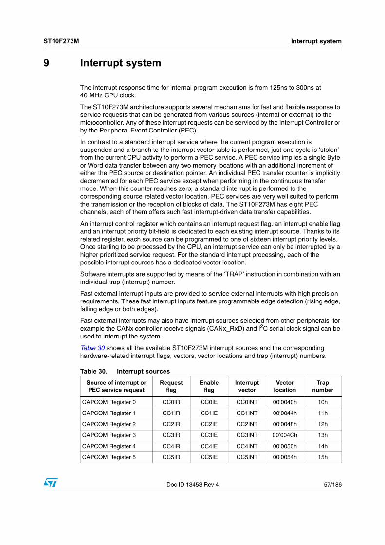
ST10F273M Interrupt system
Doc ID 13453 Rev 4 57/186
9 Interrupt system
The interrupt response time for internal program execution is from 125ns to 300ns at 40 MHz CPU clock.
The ST10F273M architecture supports several mechanisms for fast and flexible response to service requests that can be generated from various sources (internal or external) to the microcontroller. Any of these interrupt requests can be serviced by the Interrupt Controller or by the Peripheral Event Controller (PEC).
In contrast to a standard interrupt service where the current program execution is suspended and a branch to the interrupt vector table is performed, just one cycle is ‘stolen’ from the current CPU activity to perform a PEC service. A PEC service implies a single Byte or Word data transfer between any two memory locations with an additional increment of either the PEC source or destination pointer. An individual PEC transfer counter is implicitly decremented for each PEC service except when performing in the continuous transfer mode. When this counter reaches zero, a standard interrupt is performed to the corresponding source related vector location. PEC services are very well suited to perform the transmission or the reception of blocks of data. The ST10F273M has eight PEC channels, each of them offers such fast interrupt-driven data transfer capabilities.
An interrupt control register which contains an interrupt request flag, an interrupt enable flag and an interrupt priority bit-field is dedicated to each existing interrupt source. Thanks to its related register, each source can be programmed to one of sixteen interrupt priority levels. Once starting to be processed by the CPU, an interrupt service can only be interrupted by a higher prioritized service request. For the standard interrupt processing, each of the possible interrupt sources has a dedicated vector location.
Software interrupts are supported by means of the ‘TRAP’ instruction in combination with an individual trap (interrupt) number.
Fast external interrupt inputs are provided to service external interrupts with high precision requirements. These fast interrupt inputs feature programmable edge detection (rising edge, falling edge or both edges).
Fast external interrupts may also have interrupt sources selected from other peripherals; for example the CANx controller receive signals (CANx_RxD) and I2C serial clock signal can be used to interrupt the system.
Table 30 shows all the available ST10F273M interrupt sources and the corresponding hardware-related interrupt flags, vectors, vector locations and trap (interrupt) numbers.
Table 30. Interrupt sources
Source of interrupt or PEC service request
Requestflag
Enableflag
Interruptvector
Vectorlocation
Trapnumber
CAPCOM Register 0 CC0IR CC0IE CC0INT 00’0040h 10h
CAPCOM Register 1 CC1IR CC1IE CC1INT 00’0044h 11h
CAPCOM Register 2 CC2IR CC2IE CC2INT 00’0048h 12h
CAPCOM Register 3 CC3IR CC3IE CC3INT 00’004Ch 13h
CAPCOM Register 4 CC4IR CC4IE CC4INT 00’0050h 14h
CAPCOM Register 5 CC5IR CC5IE CC5INT 00’0054h 15h

Interrupt system ST10F273M
58/186 Doc ID 13453 Rev 4
CAPCOM Register 6 CC6IR CC6IE CC6INT 00’0058h 16h
CAPCOM Register 7 CC7IR CC7IE CC7INT 00’005Ch 17h
CAPCOM Register 8 CC8IR CC8IE CC8INT 00’0060h 18h
CAPCOM Register 9 CC9IR CC9IE CC9INT 00’0064h 19h
CAPCOM Register 10 CC10IR CC10IE CC10INT 00’0068h 1Ah
CAPCOM Register 11 CC11IR CC11IE CC11INT 00’006Ch 1Bh
CAPCOM Register 12 CC12IR CC12IE CC12INT 00’0070h 1Ch
CAPCOM Register 13 CC13IR CC13IE CC13INT 00’0074h 1Dh
CAPCOM Register 14 CC14IR CC14IE CC14INT 00’0078h 1Eh
CAPCOM Register 15 CC15IR CC15IE CC15INT 00’007Ch 1Fh
CAPCOM Register 16 CC16IR CC16IE CC16INT 00’00C0h 30h
CAPCOM Register 17 CC17IR CC17IE CC17INT 00’00C4h 31h
CAPCOM Register 18 CC18IR CC18IE CC18INT 00’00C8h 32h
CAPCOM Register 19 CC19IR CC19IE CC19INT 00’00CCh 33h
CAPCOM Register 20 CC20IR CC20IE CC20INT 00’00D0h 34h
CAPCOM Register 21 CC21IR CC21IE CC21INT 00’00D4h 35h
CAPCOM Register 22 CC22IR CC22IE CC22INT 00’00D8h 36h
CAPCOM Register 23 CC23IR CC23IE CC23INT 00’00DCh 37h
CAPCOM Register 24 CC24IR CC24IE CC24INT 00’00E0h 38h
CAPCOM Register 25 CC25IR CC25IE CC25INT 00’00E4h 39h
CAPCOM Register 26 CC26IR CC26IE CC26INT 00’00E8h 3Ah
CAPCOM Register 27 CC27IR CC27IE CC27INT 00’00ECh 3Bh
CAPCOM Register 28 CC28IR CC28IE CC28INT 00’00F0h 3Ch
CAPCOM Register 29 CC29IR CC29IE CC29INT 00’0110h 44h
CAPCOM Register 30 CC30IR CC30IE CC30INT 00’0114h 45h
CAPCOM Register 31 CC31IR CC31IE CC31INT 00’0118h 46h
CAPCOM Timer 0 T0IR T0IE T0INT 00’0080h 20h
CAPCOM Timer 1 T1IR T1IE T1INT 00’0084h 21h
CAPCOM Timer 7 T7IR T7IE T7INT 00’00F4h 3Dh
CAPCOM Timer 8 T8IR T8IE T8INT 00’00F8h 3Eh
GPT1Timer 2 T2IR T2IE T2INT 00’0088h 22h
GPT1 Timer 3 T3IR T3IE T3INT 00’008Ch 23h
GPT1 Timer 4 T4IR T4IE T4INT 00’0090h 24h
GPT2Timer 5 T5IR T5IE T5INT 00’0094h 25h
Table 30. Interrupt sources (continued)
Source of interrupt or PEC service request
Requestflag
Enableflag
Interruptvector
Vectorlocation
Trapnumber
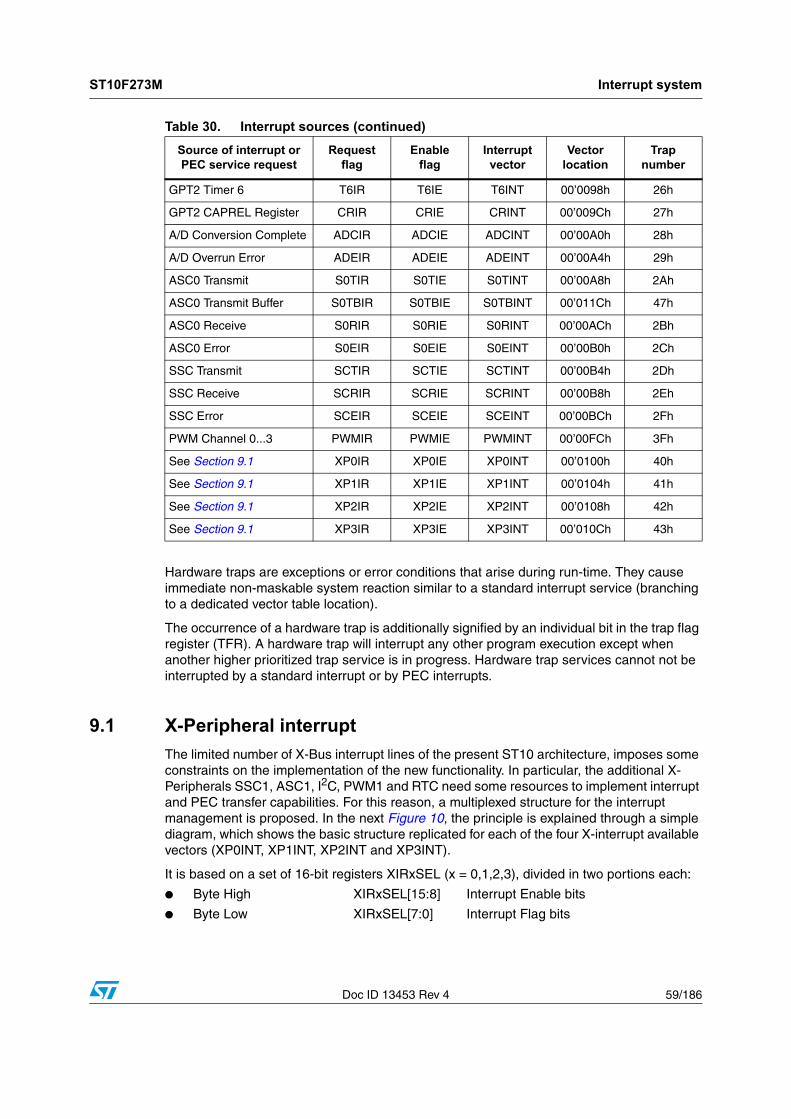
ST10F273M Interrupt system
Doc ID 13453 Rev 4 59/186
Hardware traps are exceptions or error conditions that arise during run-time. They cause immediate non-maskable system reaction similar to a standard interrupt service (branching to a dedicated vector table location).
The occurrence of a hardware trap is additionally signified by an individual bit in the trap flag register (TFR). A hardware trap will interrupt any other program execution except when another higher prioritized trap service is in progress. Hardware trap services cannot not be interrupted by a standard interrupt or by PEC interrupts.
9.1 X-Peripheral interrupt
The limited number of X-Bus interrupt lines of the present ST10 architecture, imposes some constraints on the implementation of the new functionality. In particular, the additional X-Peripherals SSC1, ASC1, I2C, PWM1 and RTC need some resources to implement interrupt and PEC transfer capabilities. For this reason, a multiplexed structure for the interrupt management is proposed. In the next Figure 10, the principle is explained through a simple diagram, which shows the basic structure replicated for each of the four X-interrupt available vectors (XP0INT, XP1INT, XP2INT and XP3INT).
It is based on a set of 16-bit registers XIRxSEL (x = 0,1,2,3), divided in two portions each:
● Byte High XIRxSEL[15:8] Interrupt Enable bits
● Byte Low XIRxSEL[7:0] Interrupt Flag bits
GPT2 Timer 6 T6IR T6IE T6INT 00’0098h 26h
GPT2 CAPREL Register CRIR CRIE CRINT 00’009Ch 27h
A/D Conversion Complete ADCIR ADCIE ADCINT 00’00A0h 28h
A/D Overrun Error ADEIR ADEIE ADEINT 00’00A4h 29h
ASC0 Transmit S0TIR S0TIE S0TINT 00’00A8h 2Ah
ASC0 Transmit Buffer S0TBIR S0TBIE S0TBINT 00’011Ch 47h
ASC0 Receive S0RIR S0RIE S0RINT 00’00ACh 2Bh
ASC0 Error S0EIR S0EIE S0EINT 00’00B0h 2Ch
SSC Transmit SCTIR SCTIE SCTINT 00’00B4h 2Dh
SSC Receive SCRIR SCRIE SCRINT 00’00B8h 2Eh
SSC Error SCEIR SCEIE SCEINT 00’00BCh 2Fh
PWM Channel 0...3 PWMIR PWMIE PWMINT 00’00FCh 3Fh
See Section 9.1 XP0IR XP0IE XP0INT 00’0100h 40h
See Section 9.1 XP1IR XP1IE XP1INT 00’0104h 41h
See Section 9.1 XP2IR XP2IE XP2INT 00’0108h 42h
See Section 9.1 XP3IR XP3IE XP3INT 00’010Ch 43h
Table 30. Interrupt sources (continued)
Source of interrupt or PEC service request
Requestflag
Enableflag
Interruptvector
Vectorlocation
Trapnumber

Interrupt system ST10F273M
60/186 Doc ID 13453 Rev 4
When different sources submit an interrupt request, the enable bits (Byte High of XIRxSEL register) define a mask which controls which sources will be associated with the unique available vector. If more than one source is enabled to issue the request, the service routine will have to take care to identify the real event to be serviced. This can easily be done by checking the flag bits (Byte Low of XIRxSEL register). Note that the flag bits can also provide information about events which are not currently serviced by the interrupt controller (since masked through the enable bits), allowing an effective software management also in absence of the possibility to serve the related interrupt request: a periodic polling of the flag bits may be implemented inside the user application.
Figure 10. X-Interrupt basic structure
Table 31 summarizes the mapping of the different interrupt sources which shares the four X-interrupt vectors.
Table 31. X-Interrupt detailed mapping
Interrupt source XP0INT XP1INT XP2INT XP3INT
CAN1 Interrupt x x
CAN2 Interrupt x x
I2C Receive x x x
I2C Transmit x x x
I2C Error x
SSC1 Receive x x x
SSC1 Transmit x x x
SSC1 Error x
ASC1 Receive x x x
ASC1 Transmit x x x
ASC1 Transmit Buffer x x x
ASC1 Error x
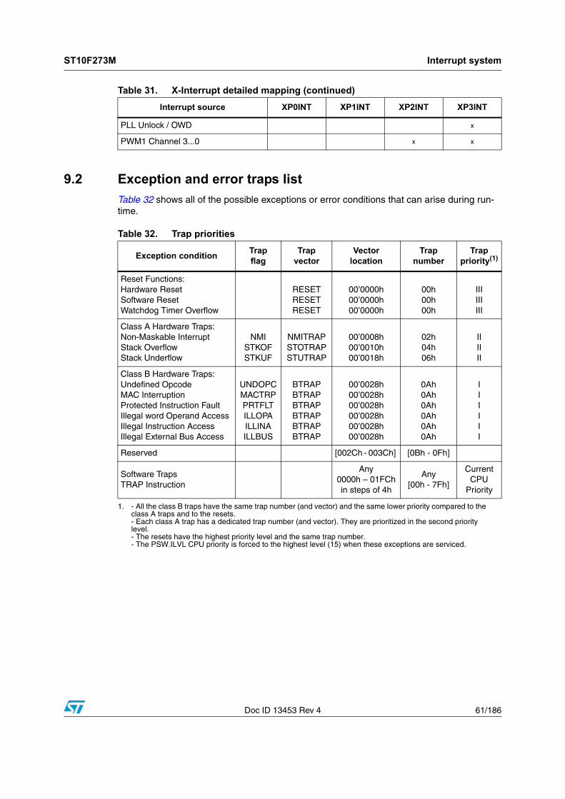
ST10F273M Interrupt system
Doc ID 13453 Rev 4 61/186
9.2 Exception and error traps list
Table 32 shows all of the possible exceptions or error conditions that can arise during run-time.
PLL Unlock / OWD x
PWM1 Channel 3...0 x x
Table 31. X-Interrupt detailed mapping (continued)
Interrupt source XP0INT XP1INT XP2INT XP3INT
Table 32. Trap priorities
Exception conditionTrapflag
Trapvector
Vectorlocation
Trapnumber
Trap priority(1)
1. - All the class B traps have the same trap number (and vector) and the same lower priority compared to the class A traps and to the resets.- Each class A trap has a dedicated trap number (and vector). They are prioritized in the second priority level.- The resets have the highest priority level and the same trap number.- The PSW.ILVL CPU priority is forced to the highest level (15) when these exceptions are serviced.
Reset Functions:Hardware ResetSoftware ResetWatchdog Timer Overflow
RESETRESETRESET
00’0000h00’0000h00’0000h
00h00h00h
IIIIIIIII
Class A Hardware Traps:Non-Maskable InterruptStack OverflowStack Underflow
NMISTKOFSTKUF
NMITRAPSTOTRAPSTUTRAP
00’0008h00’0010h00’0018h
02h04h06h
IIIIII
Class B Hardware Traps:Undefined OpcodeMAC InterruptionProtected Instruction FaultIllegal word Operand AccessIllegal Instruction AccessIllegal External Bus Access
UNDOPCMACTRPPRTFLTILLOPAILLINAILLBUS
BTRAPBTRAPBTRAPBTRAPBTRAPBTRAP
00’0028h00’0028h00’0028h00’0028h00’0028h00’0028h
0Ah0Ah0Ah0Ah0Ah0Ah
IIIIII
Reserved [002Ch - 003Ch] [0Bh - 0Fh]
Software TrapsTRAP Instruction
Any 0000h – 01FChin steps of 4h
Any[00h - 7Fh]
CurrentCPU
Priority
Capture / compare (CAPCOM) units ST10F273M
62/186 Doc ID 13453 Rev 4
10 Capture / compare (CAPCOM) units
The ST10F273M has two 16-channel CAPCOM units which support generation and control of timing sequences on up to 32 channels with a maximum resolution of 200ns at 40 MHz CPU clock.
The CAPCOM units are typically used to handle high speed I/O tasks such as pulse and waveform generation, pulse width modulation (PMW), digital to analog (D/A) conversion, software timing, or time recording relative to external events.
Four 16-bit timers (T0/T1, T7/T8) with reload registers provide two independent time bases for the capture/compare register array.
The input clock for the timers is programmable to several prescaled values of the internal system clock, or may be derived from an overflow/underflow of timer T6 in module GPT2.
This provides a wide range of variation for the timer period and resolution and allows precise adjustments to application specific requirements. In addition, external count inputs for CAPCOM timers T0 and T7 allow event scheduling for the capture/compare registers relative to external events.
Each of the two capture/compare register arrays contain 16 dual purpose capture/compare registers, each of which may be individually allocated to either CAPCOM timer T0 or T1 (T7 or T8, respectively), and programmed for capture or compare functions. Each of the 32 registers has one associated port pin which serves as an input pin for triggering the capture function, or as an output pin to indicate the occurrence of a compare event.
When a capture/compare register has been selected for capture mode, the current contents of the allocated timer will be latched (captured) into the capture/compare register in response to an external event at the port pin which is associated with this register. In addition, a specific interrupt request for this capture/compare register is generated.
Either a positive, a negative, or both a positive and a negative external signal transition at the pin can be selected as the triggering event. The contents of all registers which have been selected for one of the five compare modes are continuously compared with the contents of the allocated timers.
When a match occurs between the timer value and the value in a capture / compare register, specific actions will be taken based on the selected compare mode.
The input frequencies fTx, for the timer input selector Tx, are determined as a function of the CPU clocks. The timer input frequencies, resolution and periods which result from the selected prescaler option in TxI when using a 40 MHz CPU clock are listed in Table 34.
The numbers for the timer periods are based on a reload value of 0000h. Note that some numbers may be rounded off to three significant figures.
Table 33. Compare modes
Compare modes Function
Mode 0 Interrupt-only compare mode; several compare interrupts per timer period are possible
Mode 1 Pin toggles on each compare match; several compare events per timer period are possible
Mode 2 Interrupt-only compare mode; only one compare interrupt per timer period is generated
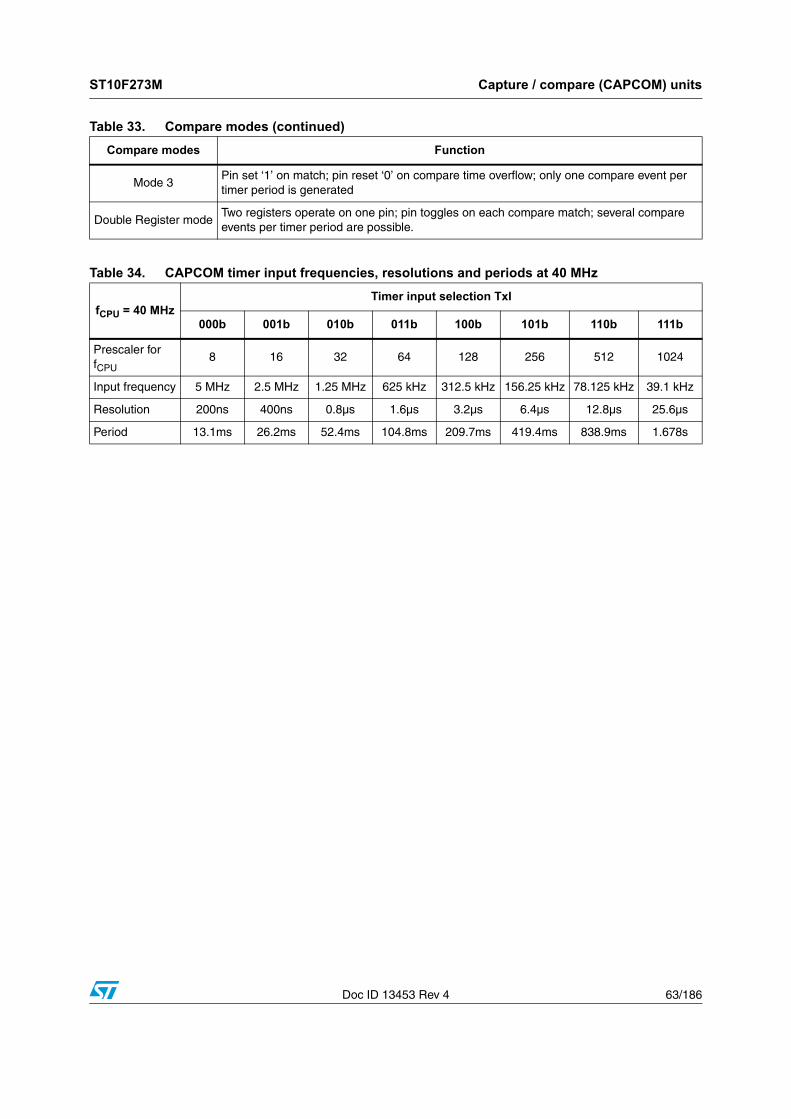
ST10F273M Capture / compare (CAPCOM) units
Doc ID 13453 Rev 4 63/186
Mode 3Pin set ‘1’ on match; pin reset ‘0’ on compare time overflow; only one compare event per timer period is generated
Double Register modeTwo registers operate on one pin; pin toggles on each compare match; several compare events per timer period are possible.
Table 33. Compare modes (continued)
Compare modes Function
Table 34. CAPCOM timer input frequencies, resolutions and periods at 40 MHz
fCPU = 40 MHzTimer input selection TxI
000b 001b 010b 011b 100b 101b 110b 111b
Prescaler for fCPU
8 16 32 64 128 256 512 1024
Input frequency 5 MHz 2.5 MHz 1.25 MHz 625 kHz 312.5 kHz 156.25 kHz 78.125 kHz 39.1 kHz
Resolution 200ns 400ns 0.8µs 1.6µs 3.2µs 6.4µs 12.8µs 25.6µs
Period 13.1ms 26.2ms 52.4ms 104.8ms 209.7ms 419.4ms 838.9ms 1.678s

General purpose timer unit ST10F273M
64/186 Doc ID 13453 Rev 4
11 General purpose timer unit
The GPT unit is a flexible multifunctional timer/counter structure which is used for time related tasks such as event timing and counting, pulse width and duty cycle measurements, pulse generation, or pulse multiplication. The GPT unit contains five 16-bit timers organized into two separate modules GPT1 and GPT2. Each timer in each module may operate independently in several different modes, or may be concatenated with another timer of the same module.
11.1 GPT1
Each of the three timers T2, T3, T4 of the GPT1 module can be configured individually for one of four basic modes of operation: timer, gated timer, counter mode and incremental interface mode.
In timer mode, the input clock for a timer is derived from the CPU clock, divided by a programmable prescaler.
In counter mode, the timer is clocked in reference to external events.
Pulse width or duty cycle measurement is supported in gated timer mode where the operation of a timer is controlled by the ‘gate’ level on an external input pin. For these purposes, each timer has one associated port pin (TxIN) which serves as gate or clock input.
Table 35 lists the timer input frequencies, resolution and periods for each prescaler option at 40 MHz CPU clock.
In Incremental Interface mode, the GPT1 timers (T2, T3, T4) can be directly connected to the incremental position sensor signals A and B by their respective inputs TxIN and TxEUD.
Direction and count signals are internally derived from these two input signals so that the contents of the respective timer Tx corresponds to the sensor position. The third position sensor signal TOP0 can be connected to an interrupt input.
Timer T3 has output toggle latches (TxOTL) which changes state on each timer over flow / underflow. The state of this latch may be output on port pins (TxOUT) for time out monitoring of external hardware components, or may be used internally to clock timers T2 and T4 for high resolution of long duration measurements.
In addition to their basic operating modes, timers T2 and T4 may be configured as reload or capture registers for timer T3.
Table 35. GPT1 timer input frequencies, resolutions and periods at 40 MHz
fCPU = 40 MHzTimer input selection T2I / T3I / T4I
000b 001b 010b 011b 100b 101b 110b 111b
Prescaler factor 8 16 32 64 128 256 512 1024
Input frequency 5 MHz 2.5 MHz 1.25 MHz 625 kHz 312.5 kHz 156.25 kHz 78.125 kHz 39.1 kHz
Resolution 200ns 400ns 0.8µs 1.6µs 3.2µs 6.4µs 12.8µs 25.6µs
Period maximum 13.1ms 26.2ms 52.4ms 104.8ms 209.7ms 419.4ms 838.9ms 1.678s

ST10F273M General purpose timer unit
Doc ID 13453 Rev 4 65/186
Figure 11. Block diagram of GPT1
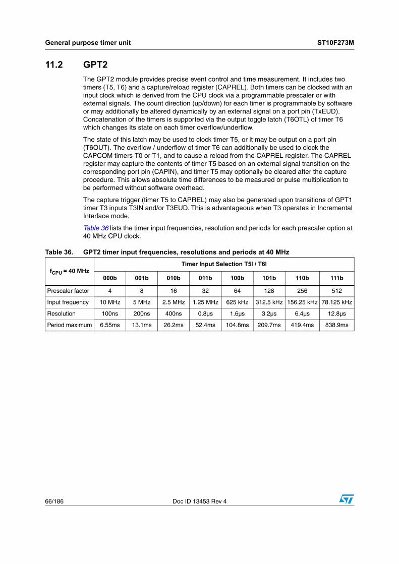
General purpose timer unit ST10F273M
66/186 Doc ID 13453 Rev 4
11.2 GPT2
The GPT2 module provides precise event control and time measurement. It includes two timers (T5, T6) and a capture/reload register (CAPREL). Both timers can be clocked with an input clock which is derived from the CPU clock via a programmable prescaler or with external signals. The count direction (up/down) for each timer is programmable by software or may additionally be altered dynamically by an external signal on a port pin (TxEUD). Concatenation of the timers is supported via the output toggle latch (T6OTL) of timer T6 which changes its state on each timer overflow/underflow.
The state of this latch may be used to clock timer T5, or it may be output on a port pin (T6OUT). The overflow / underflow of timer T6 can additionally be used to clock the CAPCOM timers T0 or T1, and to cause a reload from the CAPREL register. The CAPREL register may capture the contents of timer T5 based on an external signal transition on the corresponding port pin (CAPIN), and timer T5 may optionally be cleared after the capture procedure. This allows absolute time differences to be measured or pulse multiplication to be performed without software overhead.
The capture trigger (timer T5 to CAPREL) may also be generated upon transitions of GPT1 timer T3 inputs T3IN and/or T3EUD. This is advantageous when T3 operates in Incremental Interface mode.
Table 36 lists the timer input frequencies, resolution and periods for each prescaler option at 40 MHz CPU clock.
Table 36. GPT2 timer input frequencies, resolutions and periods at 40 MHz
fCPU = 40 MHzTimer Input Selection T5I / T6I
000b 001b 010b 011b 100b 101b 110b 111b
Prescaler factor 4 8 16 32 64 128 256 512
Input frequency 10 MHz 5 MHz 2.5 MHz 1.25 MHz 625 kHz 312.5 kHz 156.25 kHz 78.125 kHz
Resolution 100ns 200ns 400ns 0.8µs 1.6µs 3.2µs 6.4µs 12.8µs
Period maximum 6.55ms 13.1ms 26.2ms 52.4ms 104.8ms 209.7ms 419.4ms 838.9ms

ST10F273M General purpose timer unit
Doc ID 13453 Rev 4 67/186
Figure 12. Block diagram of GPT2

PWM modules ST10F273M
68/186 Doc ID 13453 Rev 4
12 PWM modules
Two pulse width modulation modules are available on ST10F273M: standard PWM0 and XBUS PWM1. They can generate up to four PWM output signals each, using edge-aligned or center-aligned PWM. In addition, the PWM modules can generate PWM burst signals and single shot outputs. Table 37 shows the PWM frequencies for different resolutions. The level of the output signals is selectable and the PWM modules can generate interrupt requests.
Figure 13. Block diagram of PWM module
Table 37. PWM unit frequencies and resolutions at 40 MHz CPU clock
Mode 0 Resolution 8-bit 10-bit 12-bit 14-bit 16-bit
CPU Clock/1 25ns 156.25 kHz 39.1 kHz 9.77 kHz 2.44 Hz 610 Hz
CPU Clock/64 1.6µs 2.44 kHz 610 Hz 152.6 Hz 38.15 Hz 9.54 Hz
Mode 1 Resolution 8-bit 10-bit 12-bit 14-bit 16-bit
CPU Clock/1 25ns 78.12 kHz 19.53 kHz 4.88 kHz 1.22 kHz 305.2 Hz
CPU Clock/64 1.6µs 1.22 kHz 305.17Hz 76.29 Hz 19.07 Hz 4.77 Hz
ST10F273M Parallel ports
Doc ID 13453 Rev 4 69/186
13 Parallel ports
13.1 Introduction
The ST10F273M MCU provides up to 111 I/O lines with programmable features. These capabilities permit this MCU to be adapted to a wide range of applications.
The ST10F273M I/O lines are organized in nine groups:
● Port 0 is a two time 8-bit port named P0L (low as less significant byte) and P0H (high as most significant byte)
● Port 1 is a two time 8-bit port named P1L and P1H
● Port 2 is a 16-bit port
● Port 3 is a 15-bit port (P3.14 line is not implemented)
● Port 4 is an 8-bit port
● Port 5 is a 16-bit port input only
● Port 6, Port 7 and Port 8 are 8-bit ports
These ports may be used as general purpose bidirectional input or output, software controlled with dedicated registers.
For example, the output drivers of six of the ports (2, 3, 4, 6, 7, 8) can be configured (bitwise) for push-pull or open drain operation using ODPx registers.
The input threshold levels are programmable (TTL/CMOS) for all the ports. The logic level of a pin is clocked into the input latch once per state time, regardless whether the port is configured for input or output. The threshold is selected with PICON and XPICON registers control bits.
A write operation to a port pin configured as an input causes the value to be written into the port output latch, while a read operation returns the latched state of the pin itself. A read-modify-write operation reads the value of the pin, modifies it, and writes it back to the output latch.
Writing to a pin configured as an output (DPx.y = ‘1’) causes the output latch and the pin to have the written value, since the output buffer is enabled. Reading this pin returns the value of the output latch. A read-modify-write operation reads the value of the output latch, modifies it, and writes it back to the output latch, thus also modifying the level at the pin.
I/O lines support an alternate function which is detailed in the following description of each port.
13.2 I/O’s special features
13.2.1 Open drain mode
Some of the I/O ports of ST10F273M support the open drain capability. This programmable feature may be used with an external pull-up resistor, in order to get an AND wired logical function.
This feature is implemented for ports P2, P3, P4, P6, P7 and P8 (see respective sections) and is controlled through the respective Open Drain Control Registers ODPx.
Parallel ports ST10F273M
70/186 Doc ID 13453 Rev 4
13.2.2 Input threshold control
The standard inputs of the ST10F273M determine the status of input signals according to TTL levels. In order to accept and recognize noisy signals, CMOS input thresholds can be selected instead of the standard TTL thresholds for all the pins. These CMOS thresholds are defined above the TTL thresholds and feature a higher hysteresis to prevent the inputs from toggling while the respective input signal level is near the thresholds.
The Port Input Control registers PICON and XPICON are used to select these thresholds for each byte of the indicated ports, this means the 8-bit ports P0L, P0H, P1L, P1H, P4, P7 and P8 are controlled by one bit each while ports P2, P3 and P5 are controlled by two bits each.
All options for individual direction and output mode control are available for each pin, independent of the selected input threshold.
13.3 Alternate port functions
Each port line has one associated programmable alternate input or output function.
● PORT0 and PORT1 may be used as address and data lines when accessing external memory. Additionally, PORT1 provides:
– Input capture lines
– 8 additional analog input channels to the A/D converter
● Port 2, Port 7 and Port 8 are associated with the capture inputs or compare outputs of the CAPCOM units and/or with the outputs of the PWM0 module, of the PWM1 module and of the ASC1.Port 2 is also used for fast external interrupt inputs and for timer 7 input.
● Port 3 includes the alternate functions of timers, serial interfaces, the optional bus control signal BHE and the system clock output (CLKOUT).
● Port 4 outputs the additional segment address bit A23...A16 in systems where more than 64 Kbytes of memory are to be access directly. In addition, CAN1, CAN2 and I2C lines are provided.
● Port 5 is used as analog input channels of the A/D converter or as timer control signals.
● Port 6 provides optional bus arbitration signals (BREQ, HLDA, HOLD) and chip select signals and the SSC1 lines.
If the alternate output function of a pin is to be used, the direction of this pin must be programmed for output (DPx.y = ‘1’), except for some signals that are used directly after reset and are configured automatically. Otherwise the pin remains in the high-impedance state and is not effected by the alternate output function. The respective port latch should hold a ‘1’, because its output is ANDed with the alternate output data (except for PWM output signals).
If the alternate input function of a pin is used, the direction of the pin must be programmed for input (DPx.y = ‘0’) if an external device is driving the pin. The input direction is the default after reset. If no external device is connected to the pin, however, the direction for this pin can also be set to output. In this case, the pin reflects the state of the port output latch. Thus, the alternate input function reads the value stored in the port output latch. This can be used for testing purposes to allow a software trigger of an alternate input function by writing to the port output latch.
On most of the port lines, the user software is responsible for setting the proper direction when using an alternate input or output function of a pin.

ST10F273M Parallel ports
Doc ID 13453 Rev 4 71/186
This is done by setting or clearing the direction control bit DPx.y of the pin before enabling the alternate function.
There are port lines, however, where the direction of the port line is switched automatically.
For instance, in the multiplexed external bus modes of PORT0, the direction must be switched several times for an instruction fetch in order to output the addresses and to input the data.
Obviously, this cannot be done through instructions. In these cases, the direction of the port line is switched automatically by hardware if the alternate function of such a pin is enabled.
To determine the appropriate level of the port output latches, check how the alternate data output is combined with the respective port latch output.
There is one basic structure for all port lines with only an alternate input function. Port lines with only an alternate output function, however, have different structures due to the way the direction of the pin is switched and depending on whether the pin is accessible by the user software or not in the alternate function mode.
All port lines that are not used for these alternate functions may be used as general purpose I/O lines.

A/D converter ST10F273M
72/186 Doc ID 13453 Rev 4
14 A/D converter
A 10-bit A/D converter with 24 multiplexed input channels and a sample and hold circuit is integrated on-chip. An automatic self-calibration adjusts the A/D converter module to process parameter variations at each reset event. The sample time (for loading the capacitors) and the conversion time is programmable and can be adjusted to the external circuitry.
The ST10F273M has 16 + 8 multiplexed input channels on Port 5 and Port 1 respectively. The selection between Port 5 and Port 1 is made via a bit in an XBus register. Refer to the User Manual for a detailed description.
A different accuracy is guaranteed (Total Unadjusted Error) on Port 5 and Port 1 analog channels (with higher restrictions when overload conditions occur); in particular, Port 5 channels are more accurate than the Port 1 channels. Refer to Section 24: Electrical characteristics for details.
The A/D converter input bandwidth is limited by the achievable accuracy: Supposing a maximum error of 0.5LSB (2mV) impacting the global TUE (TUE depends also on other causes), in worst case of temperature and process, the maximum frequency for a sine wave analog signal is around 7.5 kHz. Of course, to reduce the effect of the input signal variation on the accuracy down to 0.05LSB, the maximum input frequency of the sine wave must be reduced to 800 Hz.
If a static signal is applied during the sampling phase, a series resistance shall not be greater than 20kΩ (this taking into account eventual input leakage). It is suggested to not connect any capacitance on analog input pins, in order to reduce the effect of charge partitioning (and consequent voltage drop error) between the external and the internal capacitance: In case an RC filter is necessary, the external capacitance must be greater than 10nF to minimize the accuracy impact.
Overrun error detection / protection is controlled by the ADDAT register. Either an interrupt request is generated when the result of a previous conversion has not been read from the result register at the time the next conversion is complete, or the next conversion is suspended until the previous result has been read. For applications which require less than 16+8 analog input channels, the rning channel inputs can be used as digital input port pins.
The A/D converter of the ST10F273M supports different conversion modes:
● Single channel single conversion: The analog level of the selected channel is sampled once and converted. The result of the conversion is stored in the ADDAT register.
● Single channel continuous conversion: The analog level of the selected channel is repeatedly sampled and converted. The result of the conversion is stored in the ADDAT register.
● Auto scan single conversion: The analog level of the selected channels are sampled once and converted. After each conversion the result is stored in the ADDAT register. The data can be transferred to the RAM by interrupt software management or using the powerful Peripheral Event Controller (PEC) data transfer.
● Auto scan continuous conversion: The analog level of the selected channels are repeatedly sampled and converted. The result of the conversion is stored in the ADDAT

ST10F273M A/D converter
Doc ID 13453 Rev 4 73/186
register. The data can be transferred to the RAM by interrupt software management or using the PEC data transfer.
● Wait for ADDAT read mode: When using continuous modes, in order to avoid to overwrite the result of the current conversion by the next one, the ADWR bit of ADCON control register must be activated. Then, until the ADDAT register is read, the new result is stored in a temporary buffer and the conversion is on hold.
● Channel injection mode: When using continuous modes, a selected channel can be converted in between without changing the current operating mode. The 10-bit data of the conversion are stored in ADRES field of ADDAT2. The current continuous mode remains active after the single conversion is completed.
A full calibration sequence is performed after a reset. This full calibration lasts up to 40630 CPU clock cycles. During this time, the busy flag ADBSY is set to indicate the operation. It compensates the capacitance mismatch, so the calibration procedure does not need any update during normal operation.
No conversion can be performed during this time: The bit ADBSY shall be polled to verify when the calibration is over, and the module is able to start a conversion.

Serial channels ST10F273M
74/186 Doc ID 13453 Rev 4
15 Serial channels
Serial communication with other microcontrollers, microprocessors, terminals or external peripheral components is provided by up to four serial interfaces: two asynchronous / synchronous serial channels (ASC0 and ASC1) and two high-speed synchronous serial channel (SSC0 and SSC1). Dedicated baudrate generators set up all standard baudrates without the requirement of oscillator tuning. For transmission, reception and erroneous reception, separate interrupt vectors are provided for ASC0 and SSC0 serial channel. A more complex mechanism of interrupt sources multiplexing is implemented for ASC1 and SSC1 (XBUS mapped).
15.1 Asynchronous / synchronous serial interfaces
The asynchronous / synchronous serial interfaces (ASC0 and ASC1) provides serial communication between the ST10F273M and other microcontrollers, microprocessors or external peripherals.
15.2 ASCx in asynchronous mode
In asynchronous mode, 8- or 9-bit data transfer, parity generation and the number of stop bits can be selected. Parity framing and overrun error detection is provided to increase the reliability of data transfers. Transmission and reception of data is double-buffered. Full-duplex communication up to 1.25 Mbaud (at 40 MHz of fCPU) is supported in this mode.
Table 38. ASC asynchronous baudrates by reload value and deviation errors
S0BRS = ‘0’, fCPU = 40 MHz S0BRS = ‘1’, fCPU = 40 MHz
Baudrate (baud) Deviation errorReload value
(hex)Baudrate (baud) Deviation error
Reload value(hex)
1 250 000 0.0% / 0.0% 0000 / 0000 833 333 0.0% / 0.0% 0000 / 0000
112 000 +1.5% / -7.0% 000A / 000B 112 000 +6.3% / -7.0% 0006 / 0007
56 000 +1.5% / -3.0% 0015 / 0016 56 000 +6.3% / -0.8% 000D / 000E
38 400 +1.7% / -1.4% 001F / 0020 38 400 +3.3% / -1.4% 0014 / 0015
19 200 +0.2% / -1.4% 0040 / 0041 19 200 +0.9% / -1.4% 002A / 002B
9 600 +0.2% / -0.6% 0081 / 0082 9 600 +0.9% / -0.2% 0055 / 0056
4 800 +0.2% / -0.2% 0103 / 0104 4 800 +0.4% / -0.2% 00AC / 00AD
2 400 +0.2% / 0.0% 0207 / 0208 2 400 +0.1% / -0.2% 015A / 015B
1 200 0.1% / 0.0% 0410 / 0411 1 200 +0.1% / -0.1% 02B5 / 02B6
600 0.0% / 0.0% 0822 / 0823 600 +0.1% / 0.0% 056B / 056C
300 0.0% / 0.0% 1045 / 1046 300 0.0% / 0.0% 0AD8 / 0AD9
153 0.0% / 0.0% 1FE8 / 1FE9 102 0.0% / 0.0% 1FE8 / 1FE9

ST10F273M Serial channels
Doc ID 13453 Rev 4 75/186
Note: The deviation errors given in the Table 38 are rounded off. To avoid deviation errors use a baudrate crystal (providing a multiple of the ASC0 sampling frequency).
15.3 ASCx in synchronous mode
In synchronous mode, data is transmitted or received synchronously to a shift clock which is generated by the ST10F273M. Half-duplex communication up to 5 Mbaud (at 40 MHz of fCPU) is possible in this mode.
Note: The deviation errors given in the are rounded off. To avoid deviation errors use a baudrate crystal (providing a multiple of the ASC0 sampling frequency).
15.4 High speed synchronous serial interfaces
The High-Speed Synchronous Serial Interfaces (SSC0 and SSC1) provides flexible high-speed serial communication between the ST10F273M and other microcontrollers, microprocessors or external peripherals.
The SSCx supports full-duplex and half-duplex synchronous communication. The serial clock signal can be generated by the SSCx itself (master mode) or be received from an external master (slave mode). Data width, shift direction, clock polarity and phase are programmable.
This allows communication with SPI-compatible devices. Transmission and reception of data is double-buffered. A 16-bit baudrate generator provides the SSCx with a separate serial clock signal. The serial channel SSCx has its own dedicated 16-bit baudrate generator with 16-bit reload capability, allowing baudrate generation independent from the timers.
Table 39. ASC synchronous baudrates by reload value and deviation errors
S0BRS = ‘0’, fCPU = 40 MHz S0BRS = ‘1’, fCPU = 40 MHz
Baudrate (baud) Deviation errorReload value
(hex)Baudrate (baud) Deviation error
Reload value(hex)
5 000 000 0.0% / 0.0% 0000 / 0000 3 333 333 0.0% / 0.0% 0000 / 0000
112 000 +1.5% / -0.8% 002B / 002C 112 000 +2.6% / -0.8% 001C / 001D
56 000 +0.3% / -0.8% 0058 / 0059 56 000 +0.9% / -0.8% 003A / 003B
38 400 +0.2% / -0.6% 0081 / 0082 38 400 +0.9% / -0.2% 0055 / 0056
19 200 +0.2% / -0.2% 0103 / 0104 19 200 +0.4% / -0.2% 00AC / 00AD
9 600 +0.2% / 0.0% 0207 / 0208 9 600 +0.1% / -0.2% 015A / 015B
4 800 +0.1% / 0.0% 0410 / 0411 4 800 +0.1% / -0.1% 02B5 / 02B6
2 400 0.0% / 0.0% 0822 / 0823 2 400 +0.1% / 0.0% 056B / 056C
1 200 0.0% / 0.0% 1045 / 1046 1 200 0.0% / 0.0% 0AD8 / 0AD9
900 0.0% / 0.0% 15B2 / 15B3 600 0.0% / 0.0% 15B2 / 15B3
612 0.0% / 0.0% 1FE8 / 1FE9 407 0.0% / 0.0% 1FFD / 1FFE
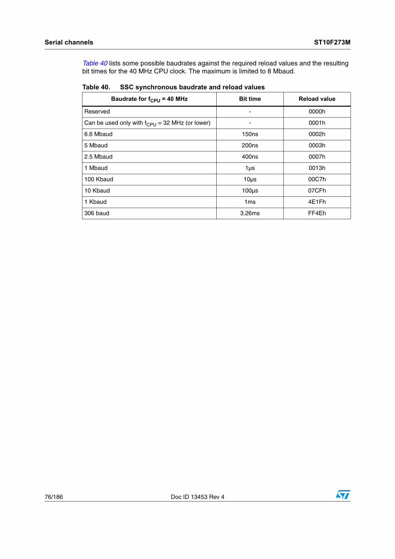
Serial channels ST10F273M
76/186 Doc ID 13453 Rev 4
Table 40 lists some possible baudrates against the required reload values and the resulting bit times for the 40 MHz CPU clock. The maximum is limited to 8 Mbaud.
Table 40. SSC synchronous baudrate and reload values
Baudrate for fCPU = 40 MHz Bit time Reload value
Reserved - 0000h
Can be used only with fCPU = 32 MHz (or lower) - 0001h
6.6 Mbaud 150ns 0002h
5 Mbaud 200ns 0003h
2.5 Mbaud 400ns 0007h
1 Mbaud 1µs 0013h
100 Kbaud 10µs 00C7h
10 Kbaud 100µs 07CFh
1 Kbaud 1ms 4E1Fh
306 baud 3.26ms FF4Eh
ST10F273M I2C interface
Doc ID 13453 Rev 4 77/186
16 I2C interface
The integrated I2C Bus Module handles the transmission and reception of frames over the two-line SDA/SCL in accordance with the I2C Bus specification. The I2C Module can operate in slave mode, in master mode or in multi-master mode. It can receive and transmit data using 7-bit or 10-bit addressing. Data can be transferred at speeds up to 400 Kbit/s (both Standard and Fast I2C bus modes are supported).
The module can generate three different types of interrupt:
● requests related to bus events, such as start or stop events, or arbitration lost
● requests related to data transmission
● requests related to data reception
These requests are issued to the interrupt controller by three different lines, and identified as Error, Transmit, and Receive interrupt lines.
When the I2C module is enabled by setting bit XI2CEN in XPERCON register, pins P4.4 and P4.7 (where SCL and SDA are respectively mapped as alternate functions) are automatically configured as bidirectional open-drain: the value of the external pull-up resistor depends on the application. P4, DP4 and ODP4 cannot influence the pin configuration.
When the I2C cell is disabled (clearing bit XI2CEN), P4.4 and P4.7 pins are standard I/ O controlled by P4, DP4 and ODP4.
The speed of the I2C interface can be selected between Standard mode (0 to 100 kHz) and Fast I2C mode (100 to 400 kHz).
CAN modules ST10F273M
78/186 Doc ID 13453 Rev 4
17 CAN modules
The two integrated CAN modules (CAN1 and CAN2) are identical and handle the completely autonomous transmission and reception of CAN frames according to the CAN specification V2.0 part B (active). It is based on the C-CAN specification.
Each on-chip CAN module can receive and transmit standard frames with 11-bit identifiers as well as extended frames with 29-bit identifiers.
Because of duplication of the CAN controllers, the following adjustments are to be considered:
● Same internal register addresses of both CAN controllers, but with base addresses differing in address bit A8; separate chip select for each CAN module. Refer to Section 4: Memory organization on page 21.
● The CAN1 transmit line (CAN1_TxD) is the alternate function of the Port P4.6 pin and the receive line (CAN1_RxD) is the alternate function of the Port P4.5 pin.
● The CAN2 transmit line (CAN2_TxD) is the alternate function of the Port P4.7 pin and the receive line (CAN2_RxD) is the alternate function of the Port P4.4 pin.
● Interrupt request lines of the CAN1 and CAN2 modules are connected to the XBUS interrupt lines together with other X-Peripherals sharing the four vectors.
● The CAN modules must be selected with corresponding CANxEN bit of XPERCON register before the bit XPEN of SYSCON register is set.
● The reset default configuration is: CAN1 enabled, CAN2 disabled.
Note: If one or both CAN modules is used, Port 4 cannot be programmed to output all eight segment address lines. Thus, only four segment address lines can be used, reducing the external memory space to 5 Mbytes (1 Mbyte per CS line).
17.1 Configuration support
It is possible that both CAN controllers are working on the same CAN bus, supporting together up to 64 message objects. In this configuration, both receive signals and both transmit signals are linked together when using the same CAN transceiver. This configuration is especially supported by providing open drain outputs for the CAN1_Txd and CAN2_TxD signals. The open drain function is controlled with the ODP4 register for port P4: in this way it is possible to connect together P4.4 with P4.5 (receive lines) and P4.6 with P4.7 (transmit lines configured to be configured as Open-Drain).
The user may also map internally both CAN modules on the same pins P4.5 and P4.6. In this way, P4.4 and P4.7 can be used either as general purpose I/O lines, or used for I2C interface. This is possible by setting bit CANPAR of the XMISC register. To access this register it is necessary to set bit XMISCEN of the XPERCON register and bit XPEN of the SYSCON register.
17.2 CAN bus configurations
Depending on the application, CAN bus configuration may be one single bus with a single or multiple interfaces or a multiple bus with a single or multiple interfaces. The ST10F273M can support both configurations.

ST10F273M CAN modules
Doc ID 13453 Rev 4 79/186
17.2.1 Single CAN bus
The single CAN bus multiple interfaces configuration may be implemented using two CAN transceivers as shown in Figure 14.
Figure 14. Connection to single CAN bus via separate CAN transceivers
The ST10F273M also supports single CAN bus multiple (dual) interfaces using the open drain option of the CANx_TxD output as shown in Figure 15. Thanks to the OR-Wired Connection, only one transceiver is required. In this case the design of the application must take in account the wire length and the noise environment.
Figure 15. Connection to single CAN bus via common CAN transceivers

CAN modules ST10F273M
80/186 Doc ID 13453 Rev 4
17.2.2 Multiple CAN bus
The ST10F273M provides two CAN interfaces to support such kind of bus configuration as shown in Figure 16.
Figure 16. Connection to two different CAN buses (for example for gateway application)
17.2.3 Parallel mode
In addition to previous configurations, a parallel mode is supported. This is shown in Figure 17.
Figure 17. Connection to one CAN bus with internal parallel mode enabled
1. P4.4 and P4.7 when not used as CAN functions can be used as general purpose I/O while they cannot be used as external bus address lines.
ST10F273M Real time clock
Doc ID 13453 Rev 4 81/186
18 Real time clock
The Real Time Clock is an independent timer, in which the clock is derived directly from the clock oscillator on XTAL1 (main oscillator) input or XTAL3 input (32 kHz low-power oscillator) so that it can continue running even in Idle or Power-down modes (if so enabled). Registers access is implemented onto the XBUS. This module is designed with the following characteristics:
● generation of the current time and date for the system
● cyclic time based interrupt, on Port2 external interrupts every “RTC basic clock tick” and after n ’RTC basic clock ticks’ (n is programmable) if enabled
● 58-bit timer for long term measurement
● capability to exit the ST10 chip from Power-down mode (if PWDCFG of SYSCON set) after a programmed delay
The real time clock is based on two main blocks of counters. The first block is a prescaler which generates a basic reference clock (for example, a 1 second period). This basic reference clock is provided by the 20-bit DIVIDER. This 20-bit counter is driven by an input clock derived from the on-chip CPU clock, predivided by a 1/64 fixed counter. This 20-bit counter is loaded at each basic reference clock period with the value of the 20-bit PRESCALER register. The value of the 20-bit RTCP register determines the period of the basic reference clock.
A timed interrupt request (RTCSI) may be sent on each basic reference clock period. The second block of the RTC is a 32-bit counter that may be initialized with the current system time. This counter is driven with the basic reference clock signal. In order to provide an alarm function the contents of the counter is compared with a 32-bit alarm register. The alarm register may be loaded with a reference date. An alarm interrupt request (RTCAI), may be generated when the value of the counter matches the alarm register.
The timed RTCSI and the alarm RTCAI interrupt requests can trigger a fast external interrupt via the EXISEL register of port 2 and wake up the ST10 chip when running power-down mode. Using the RTCOFF bit of the RTCCON register, the user may switch off the clock oscillator when entering the power-down mode.
The last function implemented in the RTC is to switch off the main on-chip oscillator and the 32 kHz on chip oscillator if the ST10 enters the Power-down mode, so that the chip can be fully switched off (if RTC is disabled).
At power-on, and after Reset phase, if the presence of a 32 kHz oscillation on XTAL3 / XTAL4 pins is detected, then the RTC counter is driven by this low frequency reference clock: when Power-down mode is entered, the RTC can either be stopped or left running, and in both the cases the main oscillator is turned off, reducing the power consumption of the device to the minimum required to keep on running the RTC counter and relative reference oscillator. This is also valid if Standby mode is entered (switching off the main supply VDD), since both the RTC and the low power oscillator (32 kHz) are biased by the VSTBY. Vice versa, when at power on and after Reset, the 32 kHz is not present, the main oscillator drives the RTC counter, and since it is powered by the main power supply, it cannot be maintained running in Standby mode, while in Power-down mode the main oscillator is maintained running to provide the reference to the RTC module (if not disabled).
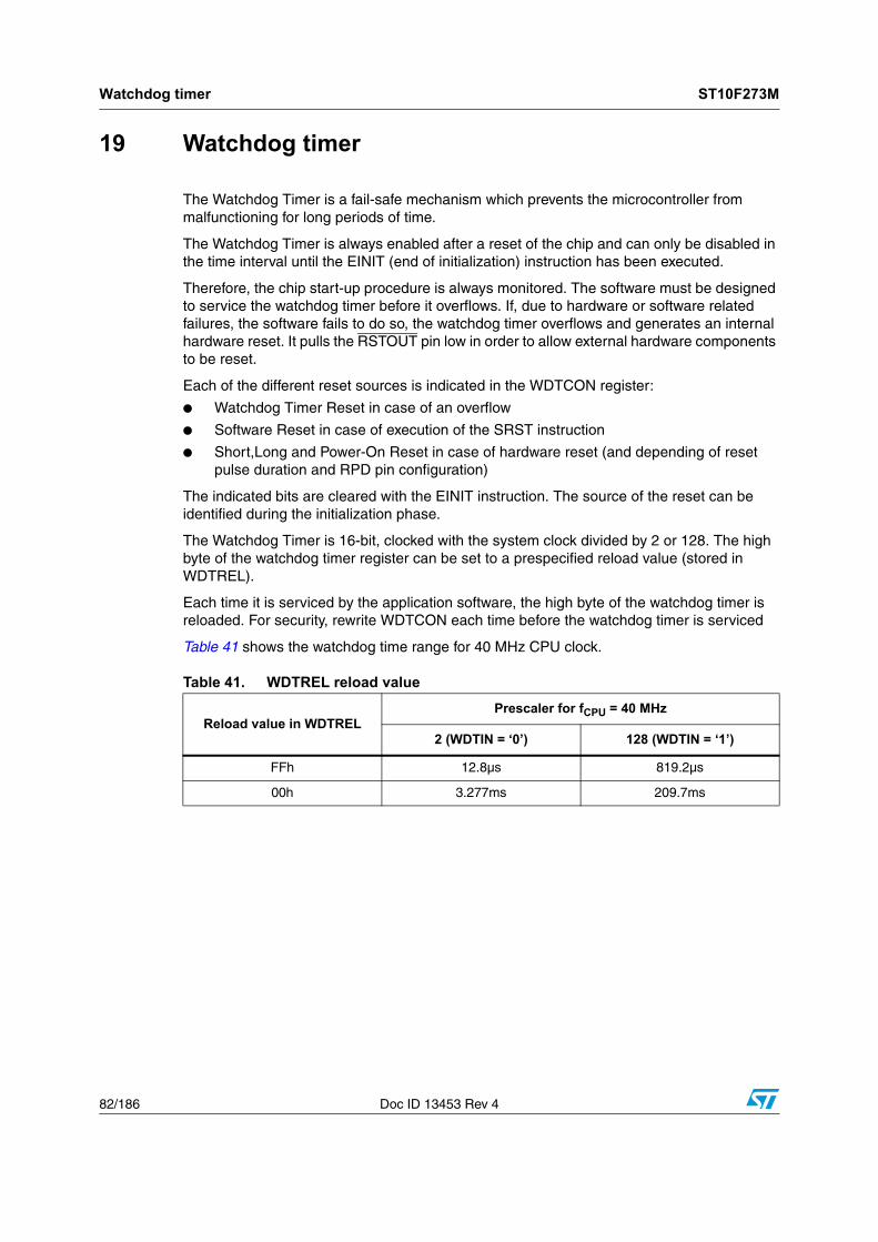
Watchdog timer ST10F273M
82/186 Doc ID 13453 Rev 4
19 Watchdog timer
The Watchdog Timer is a fail-safe mechanism which prevents the microcontroller from malfunctioning for long periods of time.
The Watchdog Timer is always enabled after a reset of the chip and can only be disabled in the time interval until the EINIT (end of initialization) instruction has been executed.
Therefore, the chip start-up procedure is always monitored. The software must be designed to service the watchdog timer before it overflows. If, due to hardware or software related failures, the software fails to do so, the watchdog timer overflows and generates an internal hardware reset. It pulls the RSTOUT pin low in order to allow external hardware components to be reset.
Each of the different reset sources is indicated in the WDTCON register:
● Watchdog Timer Reset in case of an overflow
● Software Reset in case of execution of the SRST instruction
● Short,Long and Power-On Reset in case of hardware reset (and depending of reset pulse duration and RPD pin configuration)
The indicated bits are cleared with the EINIT instruction. The source of the reset can be identified during the initialization phase.
The Watchdog Timer is 16-bit, clocked with the system clock divided by 2 or 128. The high byte of the watchdog timer register can be set to a prespecified reload value (stored in WDTREL).
Each time it is serviced by the application software, the high byte of the watchdog timer is reloaded. For security, rewrite WDTCON each time before the watchdog timer is serviced
Table 41 shows the watchdog time range for 40 MHz CPU clock.
Table 41. WDTREL reload value
Reload value in WDTRELPrescaler for fCPU = 40 MHz
2 (WDTIN = ‘0’) 128 (WDTIN = ‘1’)
FFh 12.8µs 819.2µs
00h 3.277ms 209.7ms

ST10F273M System reset
Doc ID 13453 Rev 4 83/186
20 System reset
System reset initializes the MCU in a predefined state. There are six ways to activate a reset state. The system start-up configuration is different for each case as shown in Table 42.
The figures in the upcoming sections 20.2, 20.3, 20.5 and 20.6 use the following terminology:
● transparent = level of the pin affects the internal reset logic
● not transparent = level of the pin does not affect internal logic
20.1 Input filter
On the RSTIN input pin an on-chip RC filter is implemented. It is sized to filter all spikes shorter than 50ns. On the other hand, a valid pulse longer than 500ns is required for the ST10 to recognize a reset command. In between 50ns and 500ns a pulse can either be filtered or recognized as valid, depending on the operating conditions and process variations.
For this reason all minimum durations mentioned in this chapter for the different kinds of reset events must be carefully evaluated, taking into account the above requirements.
In particular, for Short Hardware Reset, where only 4 TCL is specified as minimum input reset pulse duration, the operating frequency is a key factor.
Examples:
● For a CPU clock of 40 MHz, 4 TCL is 50ns, so it would be filtered. In this case the minimum becomes the one imposed by the filter (that is 500ns).
● For a CPU clock of 4 MHz, 4 TCL is 500ns. In this case the minimum from the formula is coherent with the limit imposed by the filter.
Table 42. Reset event definition
Reset source FlagRPD
statusConditions
Power-on reset PONR Low Power-on
Asynchronous hardware reset
LHWR
Low tRSTIN > (1)
1. RSTIN pulse should be longer than 500ns (Filter) and than settling time for configuration of Port0.
Synchronous long hardware reset
High tRSTIN > (1032 + 12)TCL + max(4 TCL, 500ns)
Synchronous short hardware reset
SHWR HightRSTIN > max(4 TCL, 500ns)tRSTIN ≤ (1032 + 12)TCL + max(4 TCL, 500ns)
Watchdog timer reset WDTR (2)
2. See next Section 20.1 for more details on minimum reset pulse duration
WDT overflow
Software reset SWR (3)
3. The RPD status has no influence unless Bidirectional Reset is activated (bit BDRSTEN in SYSCON): RPD low inhibits the Bidirectional reset on SW and WDT reset events, that is RSTIN is not activated (refer to Sections 20.4, 20.5 and 20.6).
SRST instruction execution
System reset ST10F273M
84/186 Doc ID 13453 Rev 4
20.2 Asynchronous reset
An asynchronous reset is triggered when RSTIN pin is pulled low while RPD pin is at low level. Then the ST10F273M is immediately (after the input filter delay) forced in reset default state. It pulls low RSTOUT pin, it cancels pending internal hold states if any, it aborts all internal/external bus cycles, it switches buses (data, address and control signals) and I/O pin drivers to high-impedance, it pulls high Port0 pins.
Note: If an asynchronous reset occurs during a read or write phase in internal memories, the content of the memory itself could be corrupted: To avoid this, synchronous reset usage is strongly recommended.
Power-on reset
The asynchronous reset must be used during the power-on of the device. Depending on crystal or resonator frequency, the on-chip oscillator needs about 1ms to 10ms to stabilize (refer to Section 24: Electrical characteristics), with an already stable VDD. The logic of the ST10F273M does not need a stabilized clock signal to detect an asynchronous reset, so it is suitable for power-on conditions. To ensure a proper reset sequence, the RSTIN pin and the RPD pin must be held at low level until the device clock signal is stabilized and the system configuration value on Port0 is settled.
At power-on it is important to respect some additional constraints introduced by the start-up phase of the different embedded modules.
In particular the on-chip voltage regulator needs at least 1ms to stabilize the internal 1.8V for the core logic: this time is computed from when the external reference (VDD) becomes stable (inside specification range, that is at least 4.5V). This is a constraint for the application hardware (external voltage regulator): the RSTIN pin assertion shall be extended to guarantee the voltage regulator stabilization.
A second constraint is imposed by the embedded Flash. When booting from internal memory, starting from RSTIN releasing, it needs a maximum of 1ms for its initialization: before that, the internal reset (RST signal) is not released, so the CPU does not start code execution in internal memory.
Note: This is not true if external memory is used (pin EA held low during reset phase). In this case, once RSTIN pin is released, and after few CPU clock (Filter delay plus 3...8 TCL), the internal reset signal RST is released as well, so the code execution can start immediately after. Obviously, an eventual access to the data in internal Flash is forbidden before its initialization phase is completed: an eventual access during starting phase will return FFFFh (just at the beginning), while later 009Bh (an illegal opcode trap can be generated).
At power-on, the RSTIN pin shall be tied low for a minimum time that includes also the start-up time of the main oscillator (tSTUP = 1ms for resonator, 10ms for crystal) and PLL synchronization time (tPSUP = 200µs): this means that if the internal Flash is used, the RSTIN pin could be released before the main oscillator and PLL are stable to recover some time in the start-up phase (Flash initialization only needs stable V18, but does not need stable system clock since an internal dedicated oscillator is used).
Warning: It is recommended to provide the external hardware with a current limitation circuitry. This is necessary to avoid permanent damage of the device during the power-on transient, when the capacitance on V18 pin is charged. For the on-chip voltage regulator functionality 10nF is sufficient:

ST10F273M System reset
Doc ID 13453 Rev 4 85/186
In any case, a maximum of 100nF on V18 pin should not generate problems of over-current (higher value is allowed if current is limited by the external hardware). External current limitation is nevertheless also recommended to avoid risks of damage in case of a temporary short between V18 and ground: The internal 1.8V drivers are sized to drive currents of several tens of amps, so the current must be limited by the external hardware.The limit of current is imposed by power dissipation considerations (refer to Section 24: Electrical characteristics).
In Figures 18 and 19 Asynchronous Power-on timing diagrams are shown, respectively with boot from internal or external memory, highlighting the reset phase extension introduced by the embedded IFlash module when selected.
Caution: Never power the device without keeping the RSTIN pin grounded: The device could enter into unpredictable states, risking also permanent damage.

System reset ST10F273M
86/186 Doc ID 13453 Rev 4
Figure 18. Asynchronous power-on RESET (EA = 1)

ST10F273M System reset
Doc ID 13453 Rev 4 87/186
Figure 19. Asynchronous power-on RESET (EA = 0)
1. 3 to 8 TCL depending on clock source selection
Hardware reset
The asynchronous reset must be used to recover from catastrophic situations of the application. It may be triggered by the hardware of the application. Internal hardware logic and application circuitry are described in Reset circuitry chapter and Figures 31, 32 and 33. It occurs when RSTIN is low and RPD is detected (or becomes) low as well.

System reset ST10F273M
88/186 Doc ID 13453 Rev 4
Figure 20. Asynchronous hardware RESET (EA = 1)
1. Longer than Port0 settling time + PLL synchronization (if needed, that is P0(15:13) changed).Longer than 500ns to take into account of Input Filter on RSTIN pin.

ST10F273M System reset
Doc ID 13453 Rev 4 89/186
Figure 21. Asynchronous hardware RESET (EA = 0)
1. Longer than Port0 settling time + PLL synchronization (if needed, that is P0(15:13) changed).Longer than 500ns to take into account of Input Filter on RSTIN pin.
2. 3 to 8 TCL depending on clock source selection.
Exit from asynchronous reset state
When the RSTIN pin is pulled high, the device restarts: As already mentioned, if internal Flash is used, the restarting occurs after the embedded Flash initialization routine is completed. The system configuration is latched from Port0: ALE, RD and WR/WRL pins are driven to their inactive level. The ST10F273M starts program execution from memory location 00'0000h in code segment 0. This starting location will typically point to the general initialization routine. The timings of asynchronous Hardware Reset sequence are summarized in Figure 20 and Figure 21.
20.3 Synchronous reset (warm reset)
A synchronous reset is triggered when RSTIN pin is pulled low while RPD pin is at high level. In order to properly activate the internal reset logic of the device, the RSTIN pin must be held low, at least, during 4 TCL (two periods of CPU clock): refer also to Section 20.1 for details on minimum reset pulse duration. The I/O pins are set to high impedance and RSTOUT pin is driven low. After RSTIN level is detected, a short duration of a maximum of 12 TCL (six periods of CPU clock) elapses, during which pending internal hold states are cancelled and the current internal access cycle if any is completed. External bus cycle is aborted. The internal pull-down of RSTIN pin is activated if bit BDRSTEN of SYSCON
System reset ST10F273M
90/186 Doc ID 13453 Rev 4
register was previously set by software. Note that this bit is always cleared on power-on or after a reset sequence.
Short and long synchronous reset
Once the first maximum 16 TCL are elapsed (4+12TCL), the internal reset sequence starts. It is 1024 TCL cycles long: at the end of it, and after other 8TCL the level of RSTIN is sampled (after the filter, see RSTF in the drawings): if it is already at high level, only Short Reset is flagged (refer to Chapter 19 for details on reset flags); if it is recognized still low, the Long reset is flagged as well. The major difference between Long and Short reset is that during the Long reset, also P0(15:13) become transparent, so it is possible to change the clock options.
Warning: In case of a short pulse on RSTIN pin, and when Bidirectional reset is enabled, the RSTIN pin is held low by the internal circuitry. At the end of the 1024 TCL cycles, the RTSIN pin is released, but due to the presence of the input analog filter the internal input reset signal (RSTF in the drawings) is released later (from 50 to 500ns). This delay is in parallel with the additional 8 TCL, at the end of which the internal input reset line (RSTF) is sampled, to decide if the reset event is Short or Long. In particular:
● If 8 TCL > 500ns (fCPU < 8 MHz), the reset event is always recognized as Short
● If 8 TCL < 500ns (fCPU > 8 MHz), the reset event could be recognized either as Short or Long, depending on the real filter delay (between 50 and 500ns) and the CPU frequency (RSTF sampled High means Short reset, RSTF sampled Low means Long reset). Note that in case a Long Reset is recognized, once the 8 TCL are elapsed, the P0(15:13) pins becomes transparent, so the system clock can be reconfigured. The port returns not transparent 3-4TCL after the internal RSTF signal becomes high.
The same behavior just described, occurs also when unidirectional reset is selected and RSTIN pin is held low till the end of the internal sequence (exactly 1024TCL + max 16 TCL) and released exactly at that time.
Note: When running with CPU frequency lower than 40 MHz, the minimum valid reset pulse to be recognized by the CPU (4 TCL) could be longer than the minimum analog filter delay (50ns); so it might happen that a short reset pulse is not filtered by the analog input filter, but on the other hand it is not long enough to trigger a CPU reset (shorter than 4 TCL): this would generate a Flash reset but not a system reset. In this condition, the Flash answers always with FFFFh, which leads to an illegal opcode and consequently a trap event is generated.
Exit from synchronous reset state
The reset sequence is extended until RSTIN level becomes high. Besides, it is internally prolonged by the Flash initialization when EA = 1 (internal memory selected). Then, the code execution restarts. The system configuration is latched from Port0, and ALE, RD and WR/WRL pins are driven to their inactive level. The ST10F273M starts program execution from memory location 00'0000h in code segment 0. This starting location will typically point to the general initialization routine. Timing of synchronous reset sequence are summarized in Figure 22 and Figure 23 where a Short Reset event is shown, with particular emphasis on the fact that it can degenerate into Long Reset: The two figures show the behavior when

ST10F273M System reset
Doc ID 13453 Rev 4 91/186
booting from internal or external memory respectively. Figure 24 and Figure 25 report the timing of a typical synchronous Long Reset, again when booting from internal or external memory.
Synchronous reset and RPD pin
Whenever the RSTIN pin is pulled low (by external hardware or as a consequence of a Bidirectional reset), the RPD internal weak pull-down is activated. The external capacitance (if any) on RPD pin is slowly discharged through the internal weak pull-down. If the voltage level on RPD pin reaches the input low threshold (around 2.5V), the reset event becomes immediately asynchronous. In case of hardware reset (short or long) the situation goes immediately to the one illustrated in Figure 20. There is no effect if RPD comes again above the input threshold: the asynchronous reset is completed coherently. To grant the normal completion of a synchronous reset, the value of the capacitance shall be big enough to maintain the voltage on RPD pin sufficient high along the duration of the internal reset sequence.
For a Software or Watchdog reset events, an active synchronous reset is completed regardless of the RPD status.
It is important to highlight that the signal that makes RPD status transparent under reset is the internal RSTF (after the noise filter).

System reset ST10F273M
92/186 Doc ID 13453 Rev 4
Figure 22. Synchronous short / long hardware RESET (EA = 1)
1. RSTIN assertion can be released there. Refer also to Section 21.1 for details on minimum pulse duration.
2. If during the reset condition (RSTIN low), RPD voltage drops below the threshold voltage (about 2.5V for 5V operation), the asynchronous reset is then immediately entered.
3. RSTIN pin is pulled low if bit BDRSTEN (bit 3 of SYSCON register) was previously set by software. Bit BDRSTEN is cleared after reset.
4. Minimum RSTIN low pulse duration shall also be longer than 500ns to guarantee the pulse is not masked by the internal filter (refer to Section 21.1).
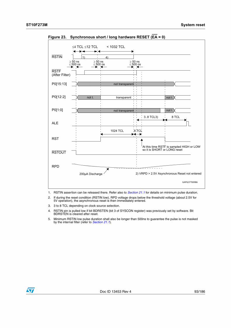
ST10F273M System reset
Doc ID 13453 Rev 4 93/186
Figure 23. Synchronous short / long hardware RESET (EA = 0)
1. RSTIN assertion can be released there. Refer also to Section 21.1 for details on minimum pulse duration.
2. If during the reset condition (RSTIN low), RPD voltage drops below the threshold voltage (about 2.5V for 5V operation), the asynchronous reset is then immediately entered.
3. 3 to 8 TCL depending on clock source selection.
4. RSTIN pin is pulled low if bit BDRSTEN (bit 3 of SYSCON register) was previously set by software. Bit BDRSTEN is cleared after reset.
5. Minimum RSTIN low pulse duration shall also be longer than 500ns to guarantee the pulse is not masked by the internal filter (refer to Section 21.1).

System reset ST10F273M
94/186 Doc ID 13453 Rev 4
Figure 24. Synchronous long hardware RESET (EA = 1)
1. If during the reset condition (RSTIN low), RPD voltage drops below the threshold voltage (about 2.5V for 5V operation), the asynchronous reset is then immediately entered. Even if RPD returns above the threshold, the reset is definitely taken as asynchronous.
2. Minimum RSTIN low pulse duration shall also be longer than 500ns to guarantee the pulse is not masked by the internal filter (refer to Section 21.1).

ST10F273M System reset
Doc ID 13453 Rev 4 95/186
Figure 25. Synchronous long hardware RESET (EA = 0)
1. If during the reset condition (RSTIN low), RPD voltage drops below the threshold voltage (about 2.5V for 5V operation), the asynchronous reset is then immediately entered.
2. Minimum RSTIN low pulse duration shall also be longer than 500ns to guarantee the pulse is not masked by the internal filter (refer to Section 21.1).
3. 3 to 8 TCL depending on clock source selection.
20.4 Software reset
A software reset sequence can be triggered at any time by the protected SRST (software reset) instruction. This instruction can be deliberately executed within a program, for example, to leave bootstrap loader mode, or on a hardware trap that reveals system failure.
On execution of the SRST instruction, the internal reset sequence is started. The microcontroller behavior is the same as for a synchronous short reset, except that only bits P0.12...P0.8 are latched at the end of the reset sequence, while previously latched, bits P0.7...P0.2 are cleared (that is written at ‘1’).
A Software reset is always taken as synchronous: there is no influence on Software Reset behavior with RPD status. In case Bidirectional Reset is selected, a Software Reset event pulls RSTIN pin low: this occurs only if RPD is high; if RPD is low, RSTIN pin is not pulled low even though Bidirectional Reset is selected.

System reset ST10F273M
96/186 Doc ID 13453 Rev 4
Refer to the next Figure 26 and Figure 27 for unidirectional SW reset timing, and to Figure 28, Figure 29 and Figure 30 for bidirectional.
20.5 Watchdog timer reset
When the watchdog timer is not disabled during the initialization, or serviced regularly during program execution, it will overflow and trigger the reset sequence.
Unlike hardware and software resets, the watchdog reset completes a running external bus cycle if this bus cycle either does not use READY, or if READY is sampled active (low) after the programmed wait states.
When READY is sampled inactive (high) after the programmed wait states the running external bus cycle is aborted. Then the internal reset sequence is started.
Bit P0.12...P0.8 are latched at the end of the reset sequence and bit P0.7...P0.2 are cleared (that is written at ‘1’).
A Watchdog reset is always taken as synchronous: there is no influence on Watchdog Reset behavior with RPD status. In case Bidirectional Reset is selected, a Watchdog Reset event pulls RSTIN pin low: this occurs only if RPD is high; if RPD is low, RSTIN pin is not pulled low even though Bidirectional Reset is selected.
Refer to the next Figure 26 and Figure 27 for unidirectional SW reset timing, and to Figure 28, Figure 29 and Figure 30 for bidirectional.
Figure 26. SW / WDT unidirectional RESET (EA = 1)
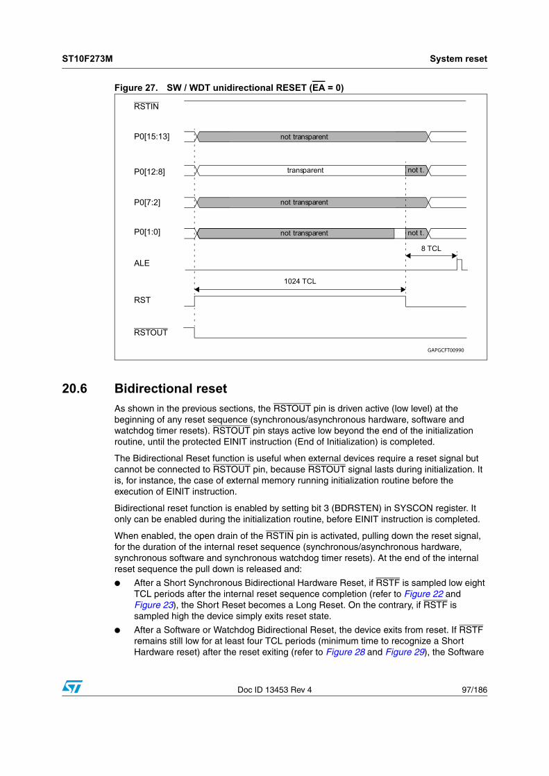
ST10F273M System reset
Doc ID 13453 Rev 4 97/186
Figure 27. SW / WDT unidirectional RESET (EA = 0)
20.6 Bidirectional reset
As shown in the previous sections, the RSTOUT pin is driven active (low level) at the beginning of any reset sequence (synchronous/asynchronous hardware, software and watchdog timer resets). RSTOUT pin stays active low beyond the end of the initialization routine, until the protected EINIT instruction (End of Initialization) is completed.
The Bidirectional Reset function is useful when external devices require a reset signal but cannot be connected to RSTOUT pin, because RSTOUT signal lasts during initialization. It is, for instance, the case of external memory running initialization routine before the execution of EINIT instruction.
Bidirectional reset function is enabled by setting bit 3 (BDRSTEN) in SYSCON register. It only can be enabled during the initialization routine, before EINIT instruction is completed.
When enabled, the open drain of the RSTIN pin is activated, pulling down the reset signal, for the duration of the internal reset sequence (synchronous/asynchronous hardware, synchronous software and synchronous watchdog timer resets). At the end of the internal reset sequence the pull down is released and:
● After a Short Synchronous Bidirectional Hardware Reset, if RSTF is sampled low eight TCL periods after the internal reset sequence completion (refer to Figure 22 and Figure 23), the Short Reset becomes a Long Reset. On the contrary, if RSTF is sampled high the device simply exits reset state.
● After a Software or Watchdog Bidirectional Reset, the device exits from reset. If RSTF remains still low for at least four TCL periods (minimum time to recognize a Short Hardware reset) after the reset exiting (refer to Figure 28 and Figure 29), the Software

System reset ST10F273M
98/186 Doc ID 13453 Rev 4
or Watchdog Reset become a Short Hardware Reset. On the contrary, if RSTF remains low for less than 4 TCL, the device simply exits reset state.
The Bidirectional reset is not effective in case RPD is held low, when a Software or Watchdog reset event occurs. On the contrary, if a Software or Watchdog Bidirectional reset event is active and RPD becomes low, the RSTIN pin is immediately released, while the internal reset sequence is completed regardless of RPD status change (1024 TCL).
Note: The bidirectional reset function is disabled by any reset sequence (bit BDRSTEN of SYSCON is cleared). To be activated again it must be enabled during the initialization routine.
WDTCON flags
Similarly to what already highlighted in the previous section when discussing about Short reset and the degeneration into Long reset, similar situations may occur when Bidirectional reset is enabled. The presence of the internal filter on RSTIN pin introduces a delay: when RSTIN is released, the internal signal after the filter (see RSTF in the drawings) is delayed, so it remains still active (low) for a while. It means that depending on the internal clock speed, a short reset may be recognized as a long reset: the WDTCON flags are set accordingly.
Besides, when either Software or Watchdog bidirectional reset events occur, again when the RSTIN pin is released (at the end of the internal reset sequence), the RSTF internal signal (after the filter) remains low for a while, and depending on the clock frequency it is recognized high or low: 8TCL after the completion of the internal sequence, the level of RSTF signal is sampled, and if recognized still low a Hardware reset sequence starts, and WDTCON will flag this last event, masking the previous one (Software or Watchdog reset). Typically, a Short Hardware reset is recognized, unless the RSTIN pin (and consequently internal signal RSTF) is sufficiently held low by the external hardware to inject a Long Hardware reset. After this occurrence, the initialization routine is not able to recognize a Software or Watchdog bidirectional reset event, since a different source is flagged inside WDTCON register. This phenomenon does not occur when internal Flash is selected during reset (EA = 1), since the initialization of the Flash itself extend the internal reset duration well beyond the filter delay.
The next Figure 28, Figure 29 and Figure 30 summarize the timing for Software and Watchdog Timer Bidirectional reset events: In particular Figure 30 shows the degeneration into Hardware reset.

ST10F273M System reset
Doc ID 13453 Rev 4 99/186
Figure 28. SW / WDT bidirectional RESET (EA = 1)
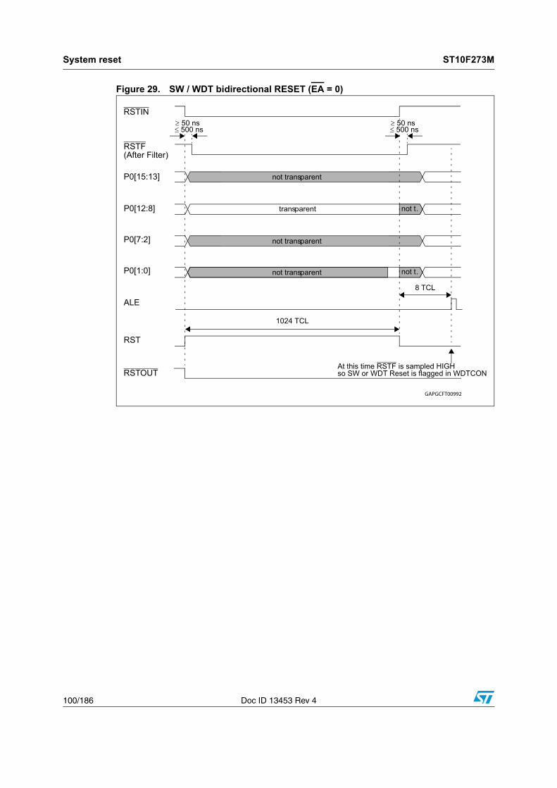
System reset ST10F273M
100/186 Doc ID 13453 Rev 4
Figure 29. SW / WDT bidirectional RESET (EA = 0)
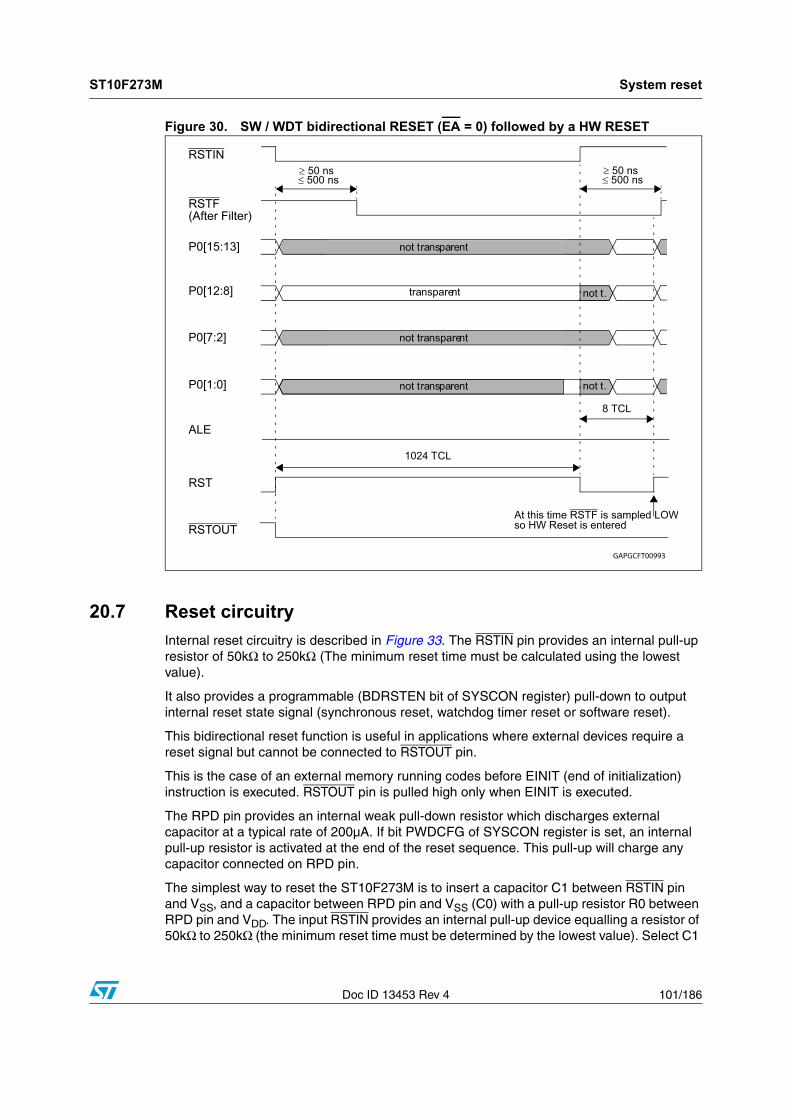
ST10F273M System reset
Doc ID 13453 Rev 4 101/186
Figure 30. SW / WDT bidirectional RESET (EA = 0) followed by a HW RESET
20.7 Reset circuitry
Internal reset circuitry is described in Figure 33. The RSTIN pin provides an internal pull-up resistor of 50kΩ to 250kΩ (The minimum reset time must be calculated using the lowest value).
It also provides a programmable (BDRSTEN bit of SYSCON register) pull-down to output internal reset state signal (synchronous reset, watchdog timer reset or software reset).
This bidirectional reset function is useful in applications where external devices require a reset signal but cannot be connected to RSTOUT pin.
This is the case of an external memory running codes before EINIT (end of initialization) instruction is executed. RSTOUT pin is pulled high only when EINIT is executed.
The RPD pin provides an internal weak pull-down resistor which discharges external capacitor at a typical rate of 200µA. If bit PWDCFG of SYSCON register is set, an internal pull-up resistor is activated at the end of the reset sequence. This pull-up will charge any capacitor connected on RPD pin.
The simplest way to reset the ST10F273M is to insert a capacitor C1 between RSTIN pin and VSS, and a capacitor between RPD pin and VSS (C0) with a pull-up resistor R0 between RPD pin and VDD. The input RSTIN provides an internal pull-up device equalling a resistor of 50kΩ to 250kΩ (the minimum reset time must be determined by the lowest value). Select C1
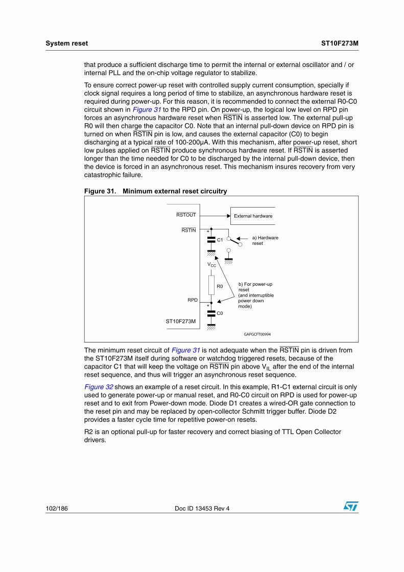
System reset ST10F273M
102/186 Doc ID 13453 Rev 4
that produce a sufficient discharge time to permit the internal or external oscillator and / or internal PLL and the on-chip voltage regulator to stabilize.
To ensure correct power-up reset with controlled supply current consumption, specially if clock signal requires a long period of time to stabilize, an asynchronous hardware reset is required during power-up. For this reason, it is recommended to connect the external R0-C0 circuit shown in Figure 31 to the RPD pin. On power-up, the logical low level on RPD pin forces an asynchronous hardware reset when RSTIN is asserted low. The external pull-up R0 will then charge the capacitor C0. Note that an internal pull-down device on RPD pin is turned on when RSTIN pin is low, and causes the external capacitor (C0) to begin discharging at a typical rate of 100-200µA. With this mechanism, after power-up reset, short low pulses applied on RSTIN produce synchronous hardware reset. If RSTIN is asserted longer than the time needed for C0 to be discharged by the internal pull-down device, then the device is forced in an asynchronous reset. This mechanism insures recovery from very catastrophic failure.
Figure 31. Minimum external reset circuitry
The minimum reset circuit of Figure 31 is not adequate when the RSTIN pin is driven from the ST10F273M itself during software or watchdog triggered resets, because of the capacitor C1 that will keep the voltage on RSTIN pin above VIL after the end of the internal reset sequence, and thus will trigger an asynchronous reset sequence.
Figure 32 shows an example of a reset circuit. In this example, R1-C1 external circuit is only used to generate power-up or manual reset, and R0-C0 circuit on RPD is used for power-up reset and to exit from Power-down mode. Diode D1 creates a wired-OR gate connection to the reset pin and may be replaced by open-collector Schmitt trigger buffer. Diode D2 provides a faster cycle time for repetitive power-on resets.
R2 is an optional pull-up for faster recovery and correct biasing of TTL Open Collector drivers.
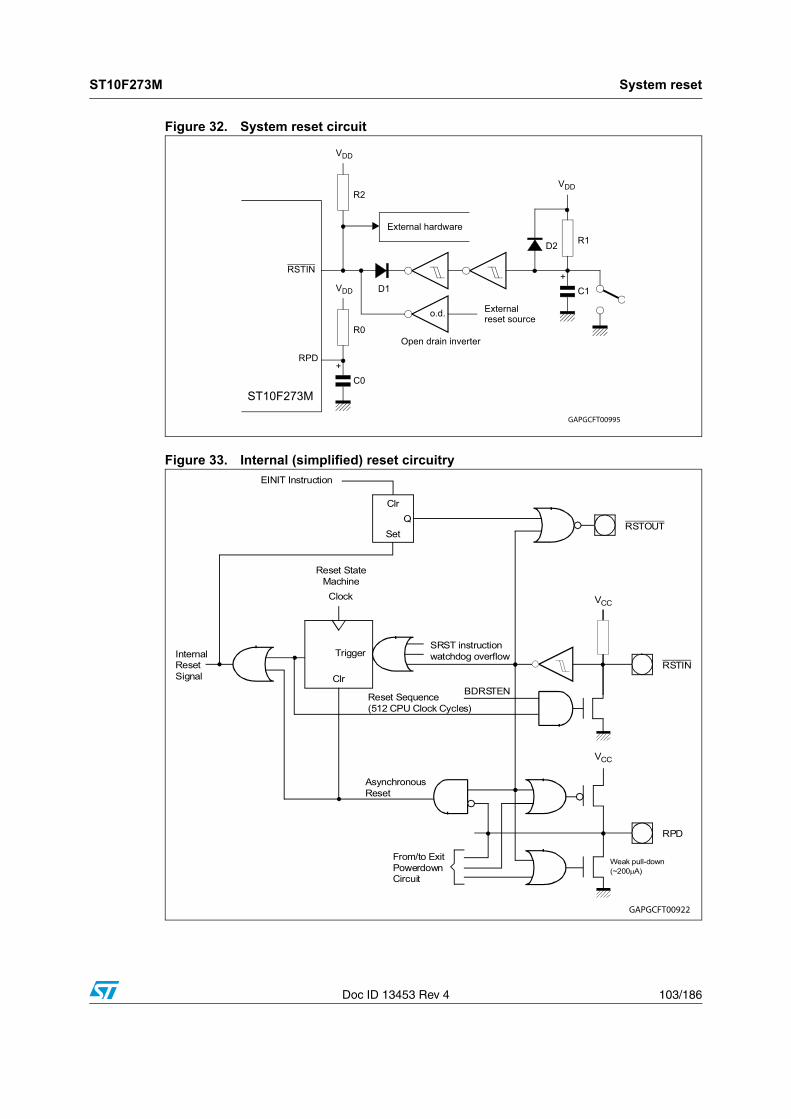
ST10F273M System reset
Doc ID 13453 Rev 4 103/186
Figure 32. System reset circuit
Figure 33. Internal (simplified) reset circuitry
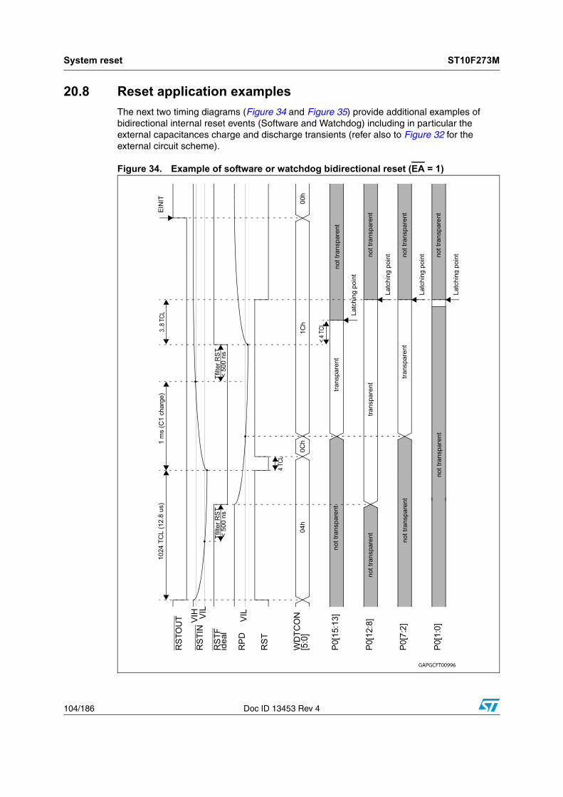
System reset ST10F273M
104/186 Doc ID 13453 Rev 4
20.8 Reset application examples
The next two timing diagrams (Figure 34 and Figure 35) provide additional examples of bidirectional internal reset events (Software and Watchdog) including in particular the external capacitances charge and discharge transients (refer also to Figure 32 for the external circuit scheme).
Figure 34. Example of software or watchdog bidirectional reset (EA = 1)
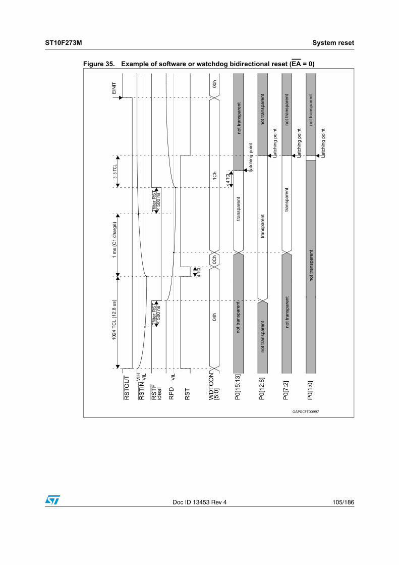
ST10F273M System reset
Doc ID 13453 Rev 4 105/186
Figure 35. Example of software or watchdog bidirectional reset (EA = 0)

System reset ST10F273M
106/186 Doc ID 13453 Rev 4
20.9 Reset summary
The following table summarizes the different reset events.
Table 43. Reset event
Event
RP
D
EA
Bid
ir
Syn
ch
.A
syn
ch. RSTIN WDTCON flags
Min Max
PO
NR
LH
WR
SH
WR
SW
R
WD
TR
Power-on Reset
0 0 N Asynch.
1 ms (VREG)1.2 ms
(Reson. + PLL)10.2 ms
(Crystal + PLL)
- 1 1 1 1 0
0 1 N Asynch. 1ms (VREG) - 1 1 1 1 0
1 x x FORBIDDEN
x x Y -
Hardware Reset(Asynchronous)
0 0 N Asynch. 500ns - 0 1 1 1 0
0 1 N Asynch. 500ns - 0 1 1 1 0
0 0 Y Asynch. 500ns - 0 1 1 1 0
0 1 Y Asynch. 500ns - 0 1 1 1 0
Short Hardware Reset
(Synchronous)(1)
1 0 N Synch. max (4 TCL, 500ns)1032 + 12 TCL +
max(4 TCL, 500ns)0 0 1 1 0
1 1 N Synch. max (4 TCL, 500ns)1032 + 12 TCL +
max(4 TCL, 500ns)0 0 1 1 0
1 0 Y Synch.max (4 TCL, 500ns)
1032 + 12 TCL +max(4 TCL, 500ns) 0 0 1 1 0
Activated by internal logic for 1024 TCL
1 1 Y Synch.max (4 TCL, 500ns)
1032 + 12 TCL +max(4 TCL, 500ns) 0 0 1 1 0
Activated by internal logic for 1024 TCL
Long Hardware Reset
(Synchronous)
1 0 N Synch.1032 + 12 TCL +
max(4 TCL, 500ns)- 0 1 1 1 0
1 1 N Synch.1032 + 12 TCL +
max(4 TCL, 500ns)- 0 1 1 1 0
1 0 Y Synch.
1032 + 12 TCL +max(4 TCL, 500ns)
-0 1 1 1 0
Activated by internal logic only for 1024 TCL
1 1 Y Synch.
1032 + 12 TCL +max(4 TCL, 500ns)
-0 1 1 1 0
Activated by internal logic only for 1024 TCL
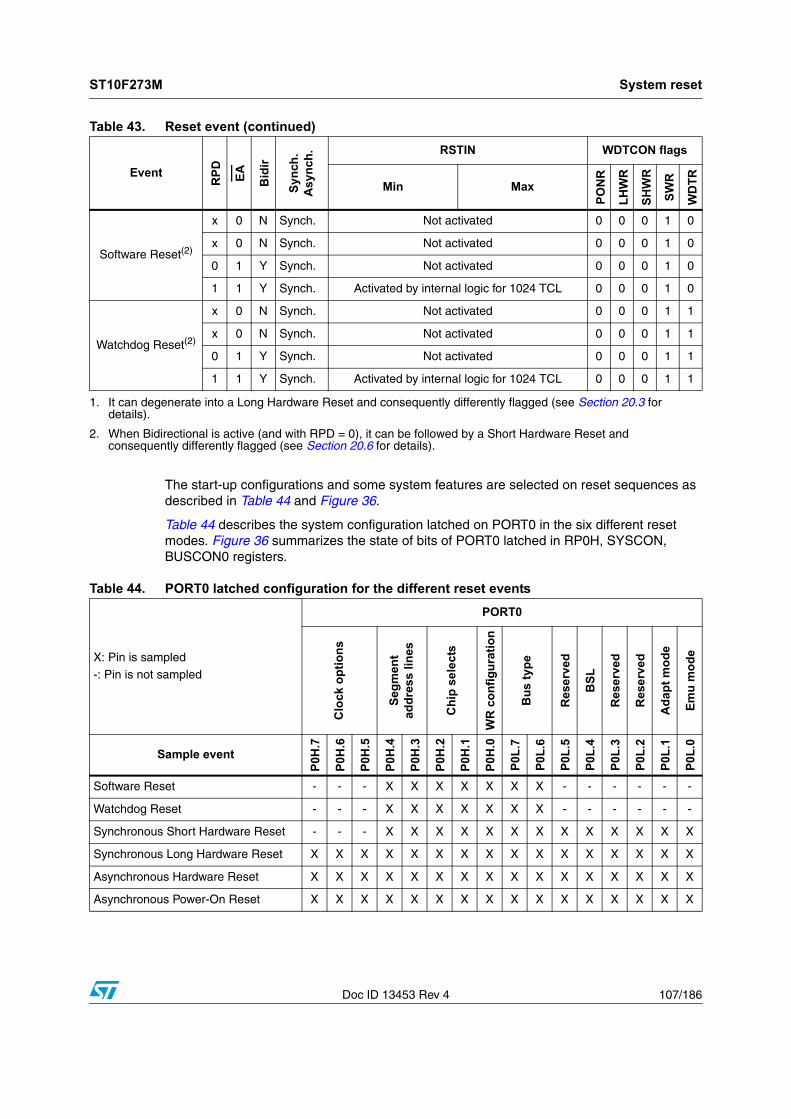
ST10F273M System reset
Doc ID 13453 Rev 4 107/186
The start-up configurations and some system features are selected on reset sequences as described in Table 44 and Figure 36.
Table 44 describes the system configuration latched on PORT0 in the six different reset modes. Figure 36 summarizes the state of bits of PORT0 latched in RP0H, SYSCON, BUSCON0 registers.
Software Reset(2)
x 0 N Synch. Not activated 0 0 0 1 0
x 0 N Synch. Not activated 0 0 0 1 0
0 1 Y Synch. Not activated 0 0 0 1 0
1 1 Y Synch. Activated by internal logic for 1024 TCL 0 0 0 1 0
Watchdog Reset(2)
x 0 N Synch. Not activated 0 0 0 1 1
x 0 N Synch. Not activated 0 0 0 1 1
0 1 Y Synch. Not activated 0 0 0 1 1
1 1 Y Synch. Activated by internal logic for 1024 TCL 0 0 0 1 1
1. It can degenerate into a Long Hardware Reset and consequently differently flagged (see Section 20.3 for details).
2. When Bidirectional is active (and with RPD = 0), it can be followed by a Short Hardware Reset and consequently differently flagged (see Section 20.6 for details).
Table 43. Reset event (continued)
Event
RP
D
EA
Bid
ir
Syn
ch.
As
ynch
. RSTIN WDTCON flags
Min Max
PO
NR
LH
WR
SH
WR
SW
R
WD
TR
Table 44. PORT0 latched configuration for the different reset events
X: Pin is sampled-: Pin is not sampled
PORT0
Clo
ck o
pti
on
s
Seg
men
tad
dre
ss li
nes
Ch
ip s
ele
cts
WR
co
nfi
gu
rati
on
Bu
s ty
pe
Res
erv
ed
BS
L
Res
erv
ed
Res
erv
ed
Ad
apt
mo
de
Em
u m
od
e
Sample event
P0H
.7
P0H
.6
P0H
.5
P0H
.4
P0H
.3
P0H
.2
P0H
.1
P0H
.0
P0
L.7
P0
L.6
P0
L.5
P0
L.4
P0
L.3
P0
L.2
P0
L.1
P0
L.0
Software Reset - - - X X X X X X X - - - - - -
Watchdog Reset - - - X X X X X X X - - - - - -
Synchronous Short Hardware Reset - - - X X X X X X X X X X X X X
Synchronous Long Hardware Reset X X X X X X X X X X X X X X X X
Asynchronous Hardware Reset X X X X X X X X X X X X X X X X
Asynchronous Power-On Reset X X X X X X X X X X X X X X X X

System reset ST10F273M
108/186 Doc ID 13453 Rev 4
Figure 36. PORT0 bits latched into the different registers after reset
ST10F273M Power reduction modes
Doc ID 13453 Rev 4 109/186
21 Power reduction modes
Three different power reduction modes with different levels of power reduction have been implemented in the ST10F273M. In Idle mode only the CPU is stopped, while peripherals still operate. In Power-down mode both the CPU and peripherals are stopped. In Standby mode the main power supply (VDD) can be turned off while a portion of the internal RAM remains powered via VSTBY dedicated power pin.
Idle and Power-down modes are software activated by a protected instruction and are terminated in different ways as described in the following sections.
Standby mode is entered by simply removing VDD, holding the MCU under reset state.
Note: All external bus actions are completed before Idle or Power-down mode is entered. However, Idle or Power-down mode is not entered if READY is enabled, but has not been activated (driven low for negative polarity, or driven high for positive polarity) during the last bus access.
21.1 Idle mode
Idle mode is entered by running the IDLE protected instruction. The CPU operation is stopped and the peripherals still run.
Idle mode is terminated by any interrupt request. Whether or not the interrupt is serviced, the instruction following the IDLE instruction will be executed after the return from interrupt (RETI) instruction, and the CPU then resumes the normal program.
21.2 Power-down mode
Power-down mode starts by running the PWRDN protected instruction. The internal clock is stopped and all MCU parts including the watchdog timer are on hold. The only exception could be the Real Time Clock if programmed accordingly in conjuction with selecting one of the two oscillator circuits (either the main or the 32 kHz on-chip oscillator).
If the Real Time Clock module is used when the device is in Power-down mode, a reference clock is needed. In this case, two possible configurations may be selected by the user application according to the desired level of power reduction:
● A 32 kHz crystal is connected to the on-chip low-power oscillator (pins XTAL3 / XTAL4) and running. In this case the main oscillator is stopped when Power-down mode is entered, while the Real Time Clock continues counting using a 32 kHz clock signal as reference. The presence of a running low-power oscillator is detected after the Power-on: This clock is immediately assumed (if present, or as soon as it is detected) as reference for the Real Time Clock counter and it will be maintained indefinitely (unless specifically disabled via software).
● Only the main oscillator is running (XTAL1 / XTAL2 pins). In this case the main oscillator is not stopped when Power-down is entered, and the Real Time Clock continues counting using the main oscillator clock signal as reference.
There are two different operating Power-down modes: protected mode and interruptible mode.
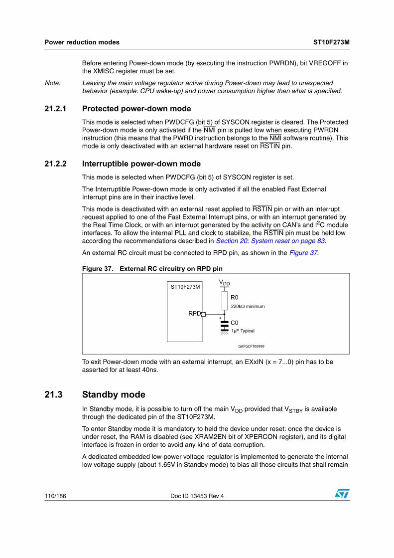
Power reduction modes ST10F273M
110/186 Doc ID 13453 Rev 4
Before entering Power-down mode (by executing the instruction PWRDN), bit VREGOFF in the XMISC register must be set.
Note: Leaving the main voltage regulator active during Power-down may lead to unexpected behavior (example: CPU wake-up) and power consumption higher than what is specified.
21.2.1 Protected power-down mode
This mode is selected when PWDCFG (bit 5) of SYSCON register is cleared. The Protected Power-down mode is only activated if the NMI pin is pulled low when executing PWRDN instruction (this means that the PWRD instruction belongs to the NMI software routine). This mode is only deactivated with an external hardware reset on RSTIN pin.
21.2.2 Interruptible power-down mode
This mode is selected when PWDCFG (bit 5) of SYSCON register is set.
The Interruptible Power-down mode is only activated if all the enabled Fast External Interrupt pins are in their inactive level.
This mode is deactivated with an external reset applied to RSTIN pin or with an interrupt request applied to one of the Fast External Interrupt pins, or with an interrupt generated by the Real Time Clock, or with an interrupt generated by the activity on CAN’s and I2C module interfaces. To allow the internal PLL and clock to stabilize, the RSTIN pin must be held low according the recommendations described in Section 20: System reset on page 83.
An external RC circuit must be connected to RPD pin, as shown in the Figure 37.
Figure 37. External RC circuitry on RPD pin
To exit Power-down mode with an external interrupt, an EXxIN (x = 7...0) pin has to be asserted for at least 40ns.
21.3 Standby mode
In Standby mode, it is possible to turn off the main VDD provided that VSTBY is available through the dedicated pin of the ST10F273M.
To enter Standby mode it is mandatory to held the device under reset: once the device is under reset, the RAM is disabled (see XRAM2EN bit of XPERCON register), and its digital interface is frozen in order to avoid any kind of data corruption.
A dedicated embedded low-power voltage regulator is implemented to generate the internal low voltage supply (about 1.65V in Standby mode) to bias all those circuits that shall remain

ST10F273M Power reduction modes
Doc ID 13453 Rev 4 111/186
active: the portion of XRAM (16 Kbytes for ST10F273M), the RTC counters and 32 kHz on-chip oscillator amplifier.
In normal running mode (that is, when main VDD is on) the VSTBY pin can be tied to VSS during reset to exercise the EA functionality associated with the same pin: The voltage supply for the circuitries which are usually biased with VSTBY (see in particular the 32 kHz oscillator used in conjunction with Real Time Clock module), is granted by the active main VDD.
It must be noted that Standby mode can generate problems associated with the usage of different power supplies in CMOS systems; particular attention must be paid when the ST10F273M I/O lines are interfaced with other external CMOS integrated circuits: If VDD of ST10F273M becomes (for example, in Standby mode) lower than the output level forced by the I/O lines of these external integrated circuits, the ST10F273M could be directly powered through the inherent diode existing on ST10F273M output driver circuitry. The same is valid for ST10F273M interfaced to active/inactive communication buses during Standby mode: Current injection can be generated through the inherent diode.Furthermore, the sequence of turning on/off of the different voltage could be critical for the system (not only for the ST10F273M device). The device Standby mode current (ISTBY) may vary while VDD to VSTBY (and vice versa) transition occurs: Some current flows between VDD and VSTBY pins. System noise on both VDD and VSTBY can contribute to increase this phenomenon.
21.3.1 Entering standby mode
As already stated, to enter Standby mode the XRAM2EN bit in the XPERCON register must be cleared: This allows the RAM interface to be frozen immediately, avoiding any data corruption. As a consequence of a RESET event, the RAM power supply is switched to the internal low-voltage supply V18SB (derived from VSTBY through the low-power voltage regulator). The RAM interface remains frozen until the bit XRAM2EN is set again by software initialization routine (at next exit from main VDD power-on reset sequence).
Since V18 is falling down (as a consequence of VDD turning off), it can happen that the XRAM2EN bit is no longer able to guarantee its content (logic “0”), being the XPERCON Register powered by internal V18. This does not generate any problem, because the Standby mode switching dedicated circuit continues to confirm the RAM interface freezing, irrespective the XRAM2EN bit content; XRAM2EN bit status is considered again when internal V18 comes back over internal standby reference V18SB.
If internal V18 becomes lower than internal standby reference (V18SB) of about 0.3 to 0.45V with bit XRAM2EN set, the RAM Supply switching circuit is not active: in case of a temporary drop on internal V18 voltage versus internal V18SB during normal code execution, no spurious Standby mode switching can occur (the RAM is not frozen and can still be accessed).
The ST10F273M Core module, generating the RAM control signals, is powered by internal V18 supply; during turning off transient these control signals follow the V18, while RAM is switched to V18SB internal reference. It could happen that a high level of RAM write strobe from ST10F273M Core (active low signal) is low enough to be recognized as a logic “0” by the RAM interface (due to V18 lower than V18SB): The bus status could contain a valid address for the RAM and an unwanted data corruption could occur. For this reason, an extra interface, powered by the switched supply, is used to prevent the RAM from this kind of potential corruption mechanism.
Power reduction modes ST10F273M
112/186 Doc ID 13453 Rev 4
Warning: During power-off phase, it is important that the external hardware maintains a stable ground level on RSTIN pin, without any glitch, in order to avoid spurious exiting from reset status with unstable power supply.
21.3.2 Exiting standby mode
After the system has entered the Standby mode, the procedure to exit this mode consists of a standard Power-on sequence, with the only difference that the RAM is already powered through V18SB internal reference (derived from VSTBY pin external voltage).
It is recommended to held the device under RESET (RSTIN pin forced low) until external VDD voltage pin is stable. Even though, at the very beginning of the power-on phase, the device is maintained under reset by the internal low voltage detector circuit (implemented inside the main voltage regulator) till the internal V18 becomes higher than about 1.0V, there is no guaranty that the device stays under reset status if RSTIN is at high level during power ramp up. So, it is important the external hardware is able to guarantee a stable ground level on RSTIN along the power-on phase, without any temporary glitch.
The external hardware shall be responsible to drive low the RSTIN pin until the VDD is stable, even though the internal LVD is active.
Once the internal Reset signal goes low, the RAM (still frozen) power supply is switched to the main V18.
At this time, everything becomes stable, and the execution of the initialization routines can start: XRAM2EN bit can be set, enabling the RAM.
21.3.3 Real time clock and standby mode
When Standby mode is entered (turning off the main supply VDD), the Real Time Clock counting can be maintained running in case the on-chip 32 kHz oscillator is used to provide the reference to the counter. This is not possible if the main oscillator is used as reference for the counter: Being the main oscillator powered by VDD, once this is switched off, the oscillator is stopped.
21.3.4 Power reduction modes summary
The different Power reduction modes are summarized in the following Table 45.

ST10F273M Power reduction modes
Doc ID 13453 Rev 4 113/186
Table 45. Power reduction modes summary
Mode
VD
D
VS
TB
Y
CP
U
Per
iph
eral
s
RT
C
Mai
n O
SC
32 k
Hz
OS
C
ST
BY
XR
AM
XR
AM
Idleon on off on off run off biased biased
on on off on on run on biased biased
Power-down
on on off off off off off biased biased
on on off off on on off biased biased
on on off off on off on biased biased
Standbyoff on off off off off off biased off
off on off off on off on biased off

Programmable output clock divider ST10F273M
114/186 Doc ID 13453 Rev 4
22 Programmable output clock divider
A specific register mapped on the XBUS allows to choose the division factor on the CLKOUT signal (P3.15). This register is mapped on X-Miscellaneous memory address range.
When CLKOUT function is enabled by setting bit CLKEN of register SYSCON, by default the CPU clock is output on P3.15. Setting bit XMISCEN of register XPERCON and bit XPEN of register SYSCON, it is possible to program the clock prescaling factor: in this way on P3.15 a prescaled value of the CPU clock can be output.
When CLKOUT function is not enabled (bit CLKEN of register SYSCON cleared), P3.15 does not output any clock signal, even though XCLKOUTDIV register is programmed.
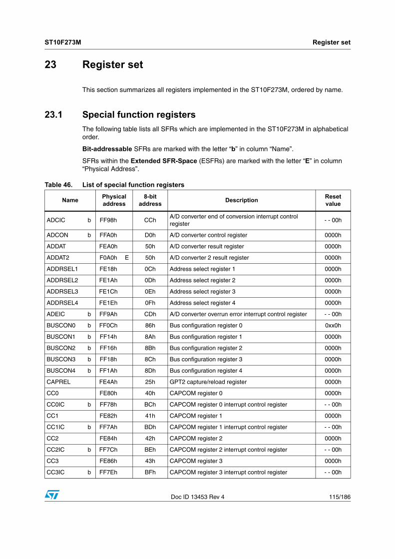
ST10F273M Register set
Doc ID 13453 Rev 4 115/186
23 Register set
This section summarizes all registers implemented in the ST10F273M, ordered by name.
23.1 Special function registers
The following table lists all SFRs which are implemented in the ST10F273M in alphabetical order.
Bit-addressable SFRs are marked with the letter “b” in column “Name”.
SFRs within the Extended SFR-Space (ESFRs) are marked with the letter “E” in column “Physical Address”.
Table 46. List of special function registers
NamePhysical address
8-bit address
DescriptionResetvalue
ADCIC b FF98h CChA/D converter end of conversion interrupt control register
- - 00h
ADCON b FFA0h D0h A/D converter control register 0000h
ADDAT FEA0h 50h A/D converter result register 0000h
ADDAT2 F0A0h E 50h A/D converter 2 result register 0000h
ADDRSEL1 FE18h 0Ch Address select register 1 0000h
ADDRSEL2 FE1Ah 0Dh Address select register 2 0000h
ADDRSEL3 FE1Ch 0Eh Address select register 3 0000h
ADDRSEL4 FE1Eh 0Fh Address select register 4 0000h
ADEIC b FF9Ah CDh A/D converter overrun error interrupt control register - - 00h
BUSCON0 b FF0Ch 86h Bus configuration register 0 0xx0h
BUSCON1 b FF14h 8Ah Bus configuration register 1 0000h
BUSCON2 b FF16h 8Bh Bus configuration register 2 0000h
BUSCON3 b FF18h 8Ch Bus configuration register 3 0000h
BUSCON4 b FF1Ah 8Dh Bus configuration register 4 0000h
CAPREL FE4Ah 25h GPT2 capture/reload register 0000h
CC0 FE80h 40h CAPCOM register 0 0000h
CC0IC b FF78h BCh CAPCOM register 0 interrupt control register - - 00h
CC1 FE82h 41h CAPCOM register 1 0000h
CC1IC b FF7Ah BDh CAPCOM register 1 interrupt control register - - 00h
CC2 FE84h 42h CAPCOM register 2 0000h
CC2IC b FF7Ch BEh CAPCOM register 2 interrupt control register - - 00h
CC3 FE86h 43h CAPCOM register 3 0000h
CC3IC b FF7Eh BFh CAPCOM register 3 interrupt control register - - 00h
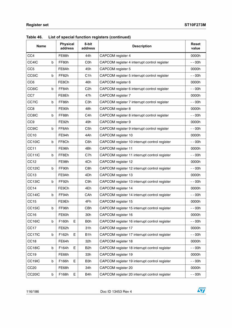
Register set ST10F273M
116/186 Doc ID 13453 Rev 4
CC4 FE88h 44h CAPCOM register 4 0000h
CC4IC b FF80h C0h CAPCOM register 4 interrupt control register - - 00h
CC5 FE8Ah 45h CAPCOM register 5 0000h
CC5IC b FF82h C1h CAPCOM register 5 interrupt control register - - 00h
CC6 FE8Ch 46h CAPCOM register 6 0000h
CC6IC b FF84h C2h CAPCOM register 6 interrupt control register - - 00h
CC7 FE8Eh 47h CAPCOM register 7 0000h
CC7IC b FF86h C3h CAPCOM register 7 interrupt control register - - 00h
CC8 FE90h 48h CAPCOM register 8 0000h
CC8IC b FF88h C4h CAPCOM register 8 interrupt control register - - 00h
CC9 FE92h 49h CAPCOM register 9 0000h
CC9IC b FF8Ah C5h CAPCOM register 9 interrupt control register - - 00h
CC10 FE94h 4Ah CAPCOM register 10 0000h
CC10IC b FF8Ch C6h CAPCOM register 10 interrupt control register - - 00h
CC11 FE96h 4Bh CAPCOM register 11 0000h
CC11IC b FF8Eh C7h CAPCOM register 11 interrupt control register - - 00h
CC12 FE98h 4Ch CAPCOM register 12 0000h
CC12IC b FF90h C8h CAPCOM register 12 interrupt control register - - 00h
CC13 FE9Ah 4Dh CAPCOM register 13 0000h
CC13IC b FF92h C9h CAPCOM register 13 interrupt control register - - 00h
CC14 FE9Ch 4Eh CAPCOM register 14 0000h
CC14IC b FF94h CAh CAPCOM register 14 interrupt control register - - 00h
CC15 FE9Eh 4Fh CAPCOM register 15 0000h
CC15IC b FF96h CBh CAPCOM register 15 interrupt control register - - 00h
CC16 FE60h 30h CAPCOM register 16 0000h
CC16IC b F160h E B0h CAPCOM register 16 interrupt control register - - 00h
CC17 FE62h 31h CAPCOM register 17 0000h
CC17IC b F162h E B1h CAPCOM register 17 interrupt control register - - 00h
CC18 FE64h 32h CAPCOM register 18 0000h
CC18IC b F164h E B2h CAPCOM register 18 interrupt control register - - 00h
CC19 FE66h 33h CAPCOM register 19 0000h
CC19IC b F166h E B3h CAPCOM register 19 interrupt control register - - 00h
CC20 FE68h 34h CAPCOM register 20 0000h
CC20IC b F168h E B4h CAPCOM register 20 interrupt control register - - 00h
Table 46. List of special function registers (continued)
NamePhysical address
8-bit address
DescriptionResetvalue

ST10F273M Register set
Doc ID 13453 Rev 4 117/186
CC4 FE88h 44h CAPCOM register 4 0000h
CC4IC b FF80h C0h CAPCOM register 4 interrupt control register - - 00h
CC5 FE8Ah 45h CAPCOM register 5 0000h
CC5IC b FF82h C1h CAPCOM register 5 interrupt control register - - 00h
CC6 FE8Ch 46h CAPCOM register 6 0000h
CC6IC b FF84h C2h CAPCOM register 6 interrupt control register - - 00h
CC7 FE8Eh 47h CAPCOM register 7 0000h
CC7IC b FF86h C3h CAPCOM register 7 interrupt control register - - 00h
CC8 FE90h 48h CAPCOM register 8 0000h
CC8IC b FF88h C4h CAPCOM register 8 interrupt control register - - 00h
CC9 FE92h 49h CAPCOM register 9 0000h
CC9IC b FF8Ah C5h CAPCOM register 9 interrupt control register - - 00h
CC10 FE94h 4Ah CAPCOM register 10 0000h
CC10IC b FF8Ch C6h CAPCOM register 10 interrupt control register - - 00h
CC11 FE96h 4Bh CAPCOM register 11 0000h
CC11IC b FF8Eh C7h CAPCOM register 11 interrupt control register - - 00h
CC12 FE98h 4Ch CAPCOM register 12 0000h
CC12IC b FF90h C8h CAPCOM register 12 interrupt control register - - 00h
CC13 FE9Ah 4Dh CAPCOM register 13 0000h
CC13IC b FF92h C9h CAPCOM register 13 interrupt control register - - 00h
CC14 FE9Ch 4Eh CAPCOM register 14 0000h
CC14IC b FF94h CAh CAPCOM register 14 interrupt control register - - 00h
CC15 FE9Eh 4Fh CAPCOM register 15 0000h
CC15IC b FF96h CBh CAPCOM register 15 interrupt control register - - 00h
CC16 FE60h 30h CAPCOM register 16 0000h
CC16IC b F160h E B0h CAPCOM register 16 interrupt control register - - 00h
CC17 FE62h 31h CAPCOM register 17 0000h
CC17IC b F162h E B1h CAPCOM register 17 interrupt control register - - 00h
CC18 FE64h 32h CAPCOM register 18 0000h
CC18IC b F164h E B2h CAPCOM register 18 interrupt control register - - 00h
CC19 FE66h 33h CAPCOM register 19 0000h
CC19IC b F166h E B3h CAPCOM register 19 interrupt control register - - 00h
CC20 FE68h 34h CAPCOM register 20 0000h
CC20IC b F168h E B4h CAPCOM register 20 interrupt control register - - 00h
Table 46. List of special function registers (continued)
NamePhysical address
8-bit address
DescriptionResetvalue

Register set ST10F273M
118/186 Doc ID 13453 Rev 4
CC21 FE6Ah 35h CAPCOM register 21 0000h
CC21IC b F16Ah E B5h CAPCOM register 21 interrupt control register - - 00h
CC22 FE6Ch 36h CAPCOM register 22 0000h
CC22IC b F16Ch E B6h CAPCOM register 22 interrupt control register - - 00h
CC23 FE6Eh 37h CAPCOM register 23 0000h
CC23IC b F16Eh E B7h CAPCOM register 23 interrupt control register - - 00h
CC24 FE70h 38h CAPCOM register 24 0000h
CC24IC b F170h E B8h CAPCOM register 24 interrupt control register - - 00h
CC25 FE72h 39h CAPCOM register 25 0000h
CC25IC b F172h E B9h CAPCOM register 25 interrupt control register - - 00h
CC26 FE74h 3Ah CAPCOM register 26 0000h
CC26IC b F174h E BAh CAPCOM register 26 interrupt control register - - 00h
CC27 FE76h 3Bh CAPCOM register 27 0000h
CC27IC b F176h E BBh CAPCOM register 27 interrupt control register - - 00h
CC28 FE78h 3Ch CAPCOM register 28 0000h
CC28IC b F178h E BCh CAPCOM register 28 interrupt control register - - 00h
CC29 FE7Ah 3Dh CAPCOM register 29 0000h
CC29IC b F184h E C2h CAPCOM register 29 interrupt control register - - 00h
CC30 FE7Ch 3Eh CAPCOM register 30 0000h
CC30IC b F18Ch E C6h CAPCOM register 30 interrupt control register - - 00h
CC31 FE7Eh 3Fh CAPCOM register 31 0000h
CC31IC b F194h E CAh CAPCOM register 31 interrupt control register - - 00h
CCM0 b FF52h A9h CAPCOM Mode Control register 0 0000h
CCM1 b FF54h AAh CAPCOM Mode Control register 1 0000h
CCM2 b FF56h ABh CAPCOM Mode Control register 2 0000h
CCM3 b FF58h ACh CAPCOM Mode Control register 3 0000h
CCM4 b FF22h 91h CAPCOM Mode Control register 4 0000h
CCM5 b FF24h 92h CAPCOM Mode Control register 5 0000h
CCM6 b FF26h 93h CAPCOM Mode Control register 6 0000h
CCM7 b FF28h 94h CAPCOM Mode Control register 7 0000h
CP FE10h 08h CPU Context Pointer register FC00h
CRIC b FF6Ah B5h GPT2 CAPREL interrupt control register - - 00h
CSP FE08h 04h CPU Code Segment Pointer register (read only) 0000h
DP0L b F100h E 80h P0L direction control register - - 00h
Table 46. List of special function registers (continued)
NamePhysical address
8-bit address
DescriptionResetvalue

ST10F273M Register set
Doc ID 13453 Rev 4 119/186
DP0H b F102h E 81h P0h direction control register - - 00h
DP1L b F104h E 82h P1L direction control register - - 00h
DP1H b F106h E 83h P1h direction control register - - 00h
DP2 b FFC2h E1h Port 2 direction control register 0000h
DP3 b FFC6h E3h Port 3 direction control register 0000h
DP4 b FFCAh E5h Port 4 direction control register - - 00h
DP6 b FFCEh E7h Port 6 direction control register - - 00h
DP7 b FFD2h E9h Port 7 direction control register - - 00h
DP8 b FFD6h EBh Port 8 direction control register - - 00h
DPP0 FE00h 00h CPU data page pointer 0 register (10-bit) 0000h
DPP1 FE02h 01h CPU data page pointer 1 register (10-bit) 0001h
DPP2 FE04h 02h CPU data page pointer 2 register (10-bit) 0002h
DPP3 FE06h 03h CPU data page pointer 3 register (10-bit) 0003h
EMUCON FE0Ah 05h Emulation control register - - XXh
EXICON b F1C0h E E0h External interrupt control register 0000h
EXISEL b F1DAh E EDh External interrupt source selection register 0000h
IDCHIP F07Ch E 3Eh Device identifier register (n is the device revision) 111nh
IDMANUF F07Eh E 3Fh Manufacturer identifier register 0403h
IDMEM F07Ah E 3Dh On-chip memory identifier register 2080h
IDPROG F078h E 3Ch Programming voltage identifier register 0040h
IDX0 b FF08h 84h MAC unit address pointer 0 0000h
IDX1 b FF0Ah 85h MAC unit address pointer 1 0000h
MAH FE5Eh 2Fh MAC unit accumulator - high word 0000h
MAL FE5Ch 2Eh MAC unit accumulator - low word 0000h
MCW b FFDCh EEh MAC unit control word 0000h
MDC b FF0Eh 87h CPU multiply divide control register 0000h
MDH FE0Ch 06h CPU multiply divide register – high word 0000h
MDL FE0Eh 07h CPU multiply divide register – low word 0000h
MRW b FFDAh EDh MAC unit repeat word 0000h
MSW b FFDEh EFh MAC unit status word 0200h
ODP2 b F1C2h E E1h Port 2 open drain control register 0000h
ODP3 b F1C6h E E3h Port 3 open drain control register 0000h
ODP4 b F1CAh E E5h Port 4 open drain control register - - 00h
ODP6 b F1CEh E E7h Port 6 open drain control register - - 00h
Table 46. List of special function registers (continued)
NamePhysical address
8-bit address
DescriptionResetvalue
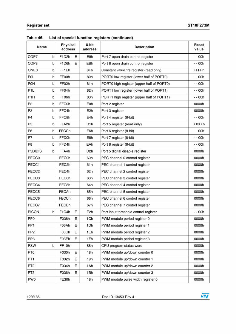
Register set ST10F273M
120/186 Doc ID 13453 Rev 4
ODP7 b F1D2h E E9h Port 7 open drain control register - - 00h
ODP8 b F1D6h E EBh Port 8 open drain control register - - 00h
ONES b FF1Eh 8Fh Constant value 1’s register (read only) FFFFh
P0L b FF00h 80h PORT0 low register (lower half of PORT0) - - 00h
P0H b FF02h 81h PORT0 high register (upper half of PORT0) - - 00h
P1L b FF04h 82h PORT1 low register (lower half of PORT1) - - 00h
P1H b FF06h 83h PORT1 high register (upper half of PORT1) - - 00h
P2 b FFC0h E0h Port 2 register 0000h
P3 b FFC4h E2h Port 3 register 0000h
P4 b FFC8h E4h Port 4 register (8-bit) - - 00h
P5 b FFA2h D1h Port 5 register (read only) XXXXh
P6 b FFCCh E6h Port 6 register (8-bit) - - 00h
P7 b FFD0h E8h Port 7 register (8-bit) - - 00h
P8 b FFD4h EAh Port 8 register (8-bit) - - 00h
P5DIDIS b FFA4h D2h Port 5 digital disable register 0000h
PECC0 FEC0h 60h PEC channel 0 control register 0000h
PECC1 FEC2h 61h PEC channel 1 control register 0000h
PECC2 FEC4h 62h PEC channel 2 control register 0000h
PECC3 FEC6h 63h PEC channel 3 control register 0000h
PECC4 FEC8h 64h PEC channel 4 control register 0000h
PECC5 FECAh 65h PEC channel 5 control register 0000h
PECC6 FECCh 66h PEC channel 6 control register 0000h
PECC7 FECEh 67h PEC channel 7 control register 0000h
PICON b F1C4h E E2h Port input threshold control register - - 00h
PP0 F038h E 1Ch PWM module period register 0 0000h
PP1 F03Ah E 1Dh PWM module period register 1 0000h
PP2 F03Ch E 1Eh PWM module period register 2 0000h
PP3 F03Eh E 1Fh PWM module period register 3 0000h
PSW b FF10h 88h CPU program status word 0000h
PT0 F030h E 18h PWM module up/down counter 0 0000h
PT1 F032h E 19h PWM module up/down counter 1 0000h
PT2 F034h E 1Ah PWM module up/down counter 2 0000h
PT3 F036h E 1Bh PWM module up/down counter 3 0000h
PW0 FE30h 18h PWM module pulse width register 0 0000h
Table 46. List of special function registers (continued)
NamePhysical address
8-bit address
DescriptionResetvalue
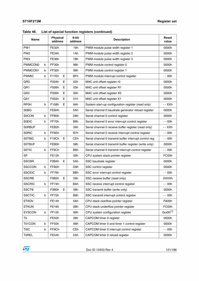
ST10F273M Register set
Doc ID 13453 Rev 4 121/186
PW1 FE32h 19h PWM module pulse width register 1 0000h
PW2 FE34h 1Ah PWM module pulse width register 2 0000h
PW3 FE36h 1Bh PWM module pulse width register 3 0000h
PWMCON0 b FF30h 98h PWM module control register 0 0000h
PWMCON1 b FF32h 99h PWM module control register 1 0000h
PWMIC b F17Eh E BFh PWM module interrupt control register - - 00h
QR0 F004h E 02h MAC unit offset register r0 0000h
QR1 F006h E 03h MAC unit offset register R1 0000h
QX0 F000h E 00h MAC unit offset register X0 0000h
QX1 F002h E 01h MAC unit offset register X1 0000h
RP0H b F108h E 84h System start-up configuration register (read only) - - XXh
S0BG FEB4h 5Ah Serial channel 0 baudrate generator reload register 0000h
S0CON b FFB0h D8h Serial channel 0 control register 0000h
S0EIC b FF70h B8h Serial channel 0 error interrupt control register - - 00h
S0RBUF FEB2h 59h Serial channel 0 receive buffer register (read only) - - XXh
S0RIC b FF6Eh B7h Serial channel 0 receive interrupt control register - - 00h
S0TBIC b F19Ch E CEh Serial channel 0 transmit buffer interrupt control reg. - - 00h
S0TBUF FEB0h 58h Serial channel 0 transmit buffer register (write only) 0000h
S0TIC b FF6Ch B6h Serial channel 0 transmit interrupt control register - - 00h
SP FE12h 09h CPU system stack pointer register FC00h
SSCBR F0B4h E 5Ah SSC baudrate register 0000h
SSCCON b FFB2h D9h SSC control register 0000h
SSCEIC b FF76h BBh SSC error interrupt control register - - 00h
SSCRB F0B2h E 59h SSC receive buffer (read only) XXXXh
SSCRIC b FF74h BAh SSC receive interrupt control register - - 00h
SSCTB F0B0h E 58h SSC transmit buffer (write only) 0000h
SSCTIC b FF72h B9h SSC transmit interrupt control register - - 00h
STKOV FE14h 0Ah CPU stack overflow pointer register FA00h
STKUN FE16h 0Bh CPU stack underflow pointer register FC00h
SYSCON b FF12h 89h CPU system configuration register 0xx0h(1)
T0 FE50h 28h CAPCOM timer 0 register 0000h
T01CON b FF50h A8h CAPCOM timer 0 and timer 1 control register 0000h
T0IC b FF9Ch CEh CAPCOM timer 0 interrupt control register - - 00h
T0REL FE54h 2Ah CAPCOM timer 0 reload register 0000h
Table 46. List of special function registers (continued)
NamePhysical address
8-bit address
DescriptionResetvalue
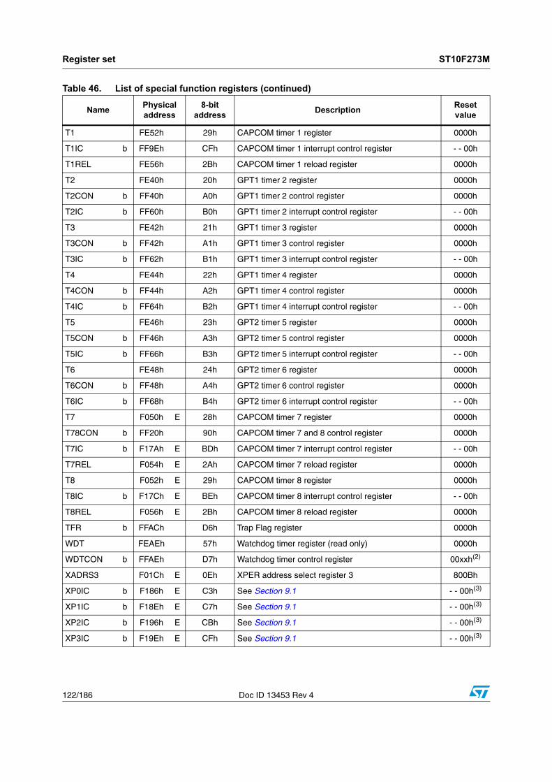
Register set ST10F273M
122/186 Doc ID 13453 Rev 4
T1 FE52h 29h CAPCOM timer 1 register 0000h
T1IC b FF9Eh CFh CAPCOM timer 1 interrupt control register - - 00h
T1REL FE56h 2Bh CAPCOM timer 1 reload register 0000h
T2 FE40h 20h GPT1 timer 2 register 0000h
T2CON b FF40h A0h GPT1 timer 2 control register 0000h
T2IC b FF60h B0h GPT1 timer 2 interrupt control register - - 00h
T3 FE42h 21h GPT1 timer 3 register 0000h
T3CON b FF42h A1h GPT1 timer 3 control register 0000h
T3IC b FF62h B1h GPT1 timer 3 interrupt control register - - 00h
T4 FE44h 22h GPT1 timer 4 register 0000h
T4CON b FF44h A2h GPT1 timer 4 control register 0000h
T4IC b FF64h B2h GPT1 timer 4 interrupt control register - - 00h
T5 FE46h 23h GPT2 timer 5 register 0000h
T5CON b FF46h A3h GPT2 timer 5 control register 0000h
T5IC b FF66h B3h GPT2 timer 5 interrupt control register - - 00h
T6 FE48h 24h GPT2 timer 6 register 0000h
T6CON b FF48h A4h GPT2 timer 6 control register 0000h
T6IC b FF68h B4h GPT2 timer 6 interrupt control register - - 00h
T7 F050h E 28h CAPCOM timer 7 register 0000h
T78CON b FF20h 90h CAPCOM timer 7 and 8 control register 0000h
T7IC b F17Ah E BDh CAPCOM timer 7 interrupt control register - - 00h
T7REL F054h E 2Ah CAPCOM timer 7 reload register 0000h
T8 F052h E 29h CAPCOM timer 8 register 0000h
T8IC b F17Ch E BEh CAPCOM timer 8 interrupt control register - - 00h
T8REL F056h E 2Bh CAPCOM timer 8 reload register 0000h
TFR b FFACh D6h Trap Flag register 0000h
WDT FEAEh 57h Watchdog timer register (read only) 0000h
WDTCON b FFAEh D7h Watchdog timer control register 00xxh(2)
XADRS3 F01Ch E 0Eh XPER address select register 3 800Bh
XP0IC b F186h E C3h See Section 9.1 - - 00h(3)
XP1IC b F18Eh E C7h See Section 9.1 - - 00h(3)
XP2IC b F196h E CBh See Section 9.1 - - 00h(3)
XP3IC b F19Eh E CFh See Section 9.1 - - 00h(3)
Table 46. List of special function registers (continued)
NamePhysical address
8-bit address
DescriptionResetvalue

ST10F273M Register set
Doc ID 13453 Rev 4 123/186
23.2 X-registers
The following table lists in order of their names all X-Bus registers which are implemented in the ST10F273M. Even though they are also physically mapped on XBus memory space, the Flash control registers are listed in a separate section.
Note: The X-Registers are not bit-addressable.
XPERCON b F024h E 12h XPER configuration register - - 05h
ZEROS b FF1Ch 8Eh Constant value 0’s register (read only) 0000h
1. The system configuration is selected during reset. SYSCON reset value is 0000 0xx0 x000 0000b.
2. Reset value depends on different triggered reset event.
3. The XPnIC Interrupt Control Registers control interrupt requests from integrated X-Bus peripherals. Some software controlled interrupt requests may be generated by setting the XPnIR bits (of XPnIC register) of the unused X-Peripheral nodes.
Table 46. List of special function registers (continued)
NamePhysical address
8-bit address
DescriptionResetvalue
Table 47. List of XBus registers
NamePhysical address
DescriptionReset value
CAN1BRPER EF0Ch CAN1: BRP extension register 0000h
CAN1BTR EF06h CAN1: Bit timing register 2301h
CAN1CR EF00h CAN1: CAN control register 0001h
CAN1EC EF04h CAN1: error counter 0000h
CAN1IF1A1 EF18h CAN1: IF1 arbitration 1 0000h
CAN1IF1A2 EF1Ah CAN1: IF1 arbitration 2 0000h
CAN1IF1CM EF12h CAN1: IF1 command mask 0000h
CAN1IF1CR EF10h CAN1: IF1 command request 0001h
CAN1IF1DA1 EF1Eh CAN1: IF1 data A 1 0000h
CAN1IF1DA2 EF20h CAN1: IF1 data A 2 0000h
CAN1IF1DB1 EF22h CAN1: IF1 data B 1 0000h
CAN1IF1DB2 EF24h CAN1: IF1 data B 2 0000h
CAN1IF1M1 EF14h CAN1: IF1 mask 1 FFFFh
CAN1IF1M2 EF16h CAN1: IF1 mask 2 FFFFh
CAN1IF1MC EF1Ch CAN1: IF1 message control 0000h
CAN1IF2A1 EF48h CAN1: IF2 arbitration 1 0000h
CAN1IF2A2 EF4Ah CAN1: IF2 arbitration 2 0000h
CAN1IF2CM EF42h CAN1: IF2 command mask 0000h
CAN1IF2CR EF40h CAN1: IF2 command request 0001h
CAN1IF2DA1 EF4Eh CAN1: IF2 data A 1 0000h

Register set ST10F273M
124/186 Doc ID 13453 Rev 4
CAN1IF2DA2 EF50h CAN1: IF2 data A 2 0000h
CAN1IF2DB1 EF52h CAN1: IF2 data B 1 0000h
CAN1IF2DB2 EF54h CAN1: IF2 data B 2 0000h
CAN1IF2M1 EF44h CAN1: IF2 Mask 1 FFFFh
CAN1IF2M2 EF46h CAN1: IF2 mask 2 FFFFh
CAN1IF2MC EF4Ch CAN1: IF2 message control 0000h
CAN1IP1 EFA0h CAN1: interrupt pending 1 0000h
CAN1IP2 EFA2h CAN1: interrupt pending 2 0000h
CAN1IR EF08h CAN1: interrupt register 0000h
CAN1MV1 EFB0h CAN1: message valid 1 0000h
CAN1MV2 EFB2h CAN1: message valid 2 0000h
CAN1ND1 EF90h CAN1: new data 1 0000h
CAN1ND2 EF92h CAN1: new data 2 0000h
CAN1SR EF02h CAN1: status register 0000h
CAN1TR EF0Ah CAN1: test register 00x0h
CAN1TR1 EF80h CAN1: transmission request 1 0000h
CAN1TR2 EF82h CAN1: transmission request 2 0000h
CAN2BRPER EE0Ch CAN2: BRP extension register 0000h
CAN2BTR EE06h CAN2: bit timing register 2301h
CAN2CR EE00h CAN2: CAN control register 0001h
CAN2EC EE04h CAN2: error counter 0000h
CAN2IF1A1 EE18h CAN2: IF1 arbitration 1 0000h
CAN2IF1A2 EE1Ah CAN2: IF1 arbitration 2 0000h
CAN2IF1CM EE12h CAN2: IF1 command mask 0000h
CAN2IF1CR EE10h CAN2: IF1 command request 0001h
CAN2IF1DA1 EE1Eh CAN2: IF1 data A 1 0000h
CAN2IF1DA2 EE20h CAN2: IF1 data A 2 0000h
CAN2IF1DB1 EE22h CAN2: IF1 data B 1 0000h
CAN2IF1DB2 EE24h CAN2: IF1 data B 2 0000h
CAN2IF1M1 EE14h CAN2: IF1 mask 1 FFFFh
CAN2IF1M2 EE16h CAN2: IF1 mask 2 FFFFh
CAN2IF1MC EE1Ch CAN2: IF1 message control 0000h
CAN2IF2A1 EE48h CAN2: IF2 arbitration 1 0000h
CAN2IF2A2 EE4Ah CAN2: IF2 arbitration 2 0000h
Table 47. List of XBus registers (continued)
NamePhysical address
DescriptionReset value

ST10F273M Register set
Doc ID 13453 Rev 4 125/186
CAN2IF2CM EE42h CAN2: IF2 command mask 0000h
CAN2IF2CR EE40h CAN2: IF2 command request 0001h
CAN2IF2DA1 EE4Eh CAN2: IF2 data A 1 0000h
CAN2IF2DA2 EE50h CAN2: IF2 data A 2 0000h
CAN2IF2DB1 EE52h CAN2: IF2 data B 1 0000h
CAN2IF2DB2 EE54h CAN2: IF2 data B 2 0000h
CAN2IF2M1 EE44h CAN2: IF2 mask 1 FFFFh
CAN2IF2M2 EE46h CAN2: IF2 mask 2 FFFFh
CAN2IF2MC EE4Ch CAN2: IF2 message control 0000h
CAN2IP1 EEA0h CAN2: interrupt pending 1 0000h
CAN2IP2 EEA2h CAN2: interrupt pending 2 0000h
CAN2IR EE08h CAN2: interrupt register 0000h
CAN2MV1 EEB0h CAN2: message valid 1 0000h
CAN2MV2 EEB2h CAN2: message valid 2 0000h
CAN2ND1 EE90h CAN2: new data 1 0000h
CAN2ND2 EE92h CAN2: new data 2 0000h
CAN2SR EE02h CAN2: status register 0000h
CAN2TR EE0Ah CAN2: test register 00x0h
CAN2TR1 EE80h CAN2: transmission request 1 0000h
CAN2TR2 EE82h CAN2: Transmission request 2 0000h
I2CCCR1 EA06h I2C clock control register 1 0000h
I2CCCR2 EA0Eh I2C clock control register 2 0000h
I2CCR EA00h I2C control register 0000h
I2CDR EA0Ch I2C data register 0000h
I2COAR1 EA08h I2C own address register 1 0000h
I2COAR2 EA0Ah I2C own address register 2 0000h
I2CSR1 EA02h I2C status register 1 0000h
I2CSR2 EA04h I2C status register 2 0000h
RTCAH ED14h RTC alarm register high byte XXXXh
RTCAL ED12h RTC alarm register low byte XXXXh
RTCCON ED00H RTC control register 000Xh
RTCDH ED0Ch RTC divider counter high byte XXXXh
RTCDL ED0Ah RTC divider counter low byte XXXXh
RTCH ED10h RTC programmable counter high byte XXXXh
Table 47. List of XBus registers (continued)
NamePhysical address
DescriptionReset value
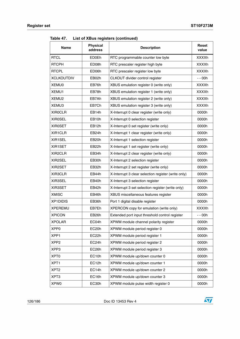
Register set ST10F273M
126/186 Doc ID 13453 Rev 4
RTCL ED0Eh RTC programmable counter low byte XXXXh
RTCPH ED08h RTC prescaler register high byte XXXXh
RTCPL ED06h RTC prescaler register low byte XXXXh
XCLKOUTDIV EB02h CLKOUT divider control register - - 00h
XEMU0 EB76h XBUS emulation register 0 (write only) XXXXh
XEMU1 EB78h XBUS emulation register 1 (write only) XXXXh
XEMU2 EB7Ah XBUS emulation register 2 (write only) XXXXh
XEMU3 EB7Ch XBUS emulation register 3 (write only) XXXXh
XIR0CLR EB14h X-Interrupt 0 clear register (write only) 0000h
XIR0SEL EB10h X-Interrupt 0 selection register 0000h
XIR0SET EB12h X-Interrupt 0 set register (write only) 0000h
XIR1CLR EB24h X-Interrupt 1 clear register (write only) 0000h
XIR1SEL EB20h X-Interrupt 1 selection register 0000h
XIR1SET EB22h X-Interrupt 1 set register (write only) 0000h
XIR2CLR EB34h X-Interrupt 2 clear register (write only) 0000h
XIR2SEL EB30h X-Interrupt 2 selection register 0000h
XIR2SET EB32h X-Interrupt 2 set register (write only) 0000h
XIR3CLR EB44h X-Interrupt 3 clear selection register (write only) 0000h
XIR3SEL EB40h X-Interrupt 3 selection register 0000h
XIR3SET EB42h X-Interrupt 3 set selection register (write only) 0000h
XMISC EB46h XBUS miscellaneous features register 0000h
XP1DIDIS EB36h Port 1 digital disable register 0000h
XPEREMU EB7Eh XPERCON copy for emulation (write only) XXXXh
XPICON EB26h Extended port input threshold control register - - 00h
XPOLAR EC04h XPWM module channel polarity register 0000h
XPP0 EC20h XPWM module period register 0 0000h
XPP1 EC22h XPWM module period register 1 0000h
XPP2 EC24h XPWM module period register 2 0000h
XPP3 EC26h XPWM module period register 3 0000h
XPT0 EC10h XPWM module up/down counter 0 0000h
XPT1 EC12h XPWM module up/down counter 1 0000h
XPT2 EC14h XPWM module up/down counter 2 0000h
XPT3 EC16h XPWM module up/down counter 3 0000h
XPW0 EC30h XPWM module pulse width register 0 0000h
Table 47. List of XBus registers (continued)
NamePhysical address
DescriptionReset value
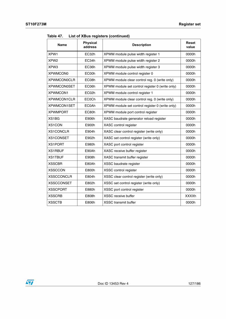
ST10F273M Register set
Doc ID 13453 Rev 4 127/186
XPW1 EC32h XPWM module pulse width register 1 0000h
XPW2 EC34h XPWM module pulse width register 2 0000h
XPW3 EC36h XPWM module pulse width register 3 0000h
XPWMCON0 EC00h XPWM module control register 0 0000h
XPWMCON0CLR EC08h XPWM module clear control reg. 0 (write only) 0000h
XPWMCON0SET EC06h XPWM module set control register 0 (write only) 0000h
XPWMCON1 EC02h XPWM module control register 1 0000h
XPWMCON1CLR EC0Ch XPWM module clear control reg. 0 (write only) 0000h
XPWMCON1SET EC0Ah XPWM module set control register 0 (write only) 0000h
XPWMPORT EC80h XPWM module port control register 0000h
XS1BG E906h XASC baudrate generator reload register 0000h
XS1CON E900h XASC control register 0000h
XS1CONCLR E904h XASC clear control register (write only) 0000h
XS1CONSET E902h XASC set control register (write only) 0000h
XS1PORT E980h XASC port control register 0000h
XS1RBUF E90Ah XASC receive buffer register 0000h
XS1TBUF E908h XASC transmit buffer register 0000h
XSSCBR E80Ah XSSC baudrate register 0000h
XSSCCON E800h XSSC control register 0000h
XSSCCONCLR E804h XSSC clear control register (write only) 0000h
XSSCCONSET E802h XSSC set control register (write only) 0000h
XSSCPORT E880h XSSC port control register 0000h
XSSCRB E808h XSSC receive buffer XXXXh
XSSCTB E806h XSSC transmit buffer 0000h
Table 47. List of XBus registers (continued)
NamePhysical address
DescriptionReset value
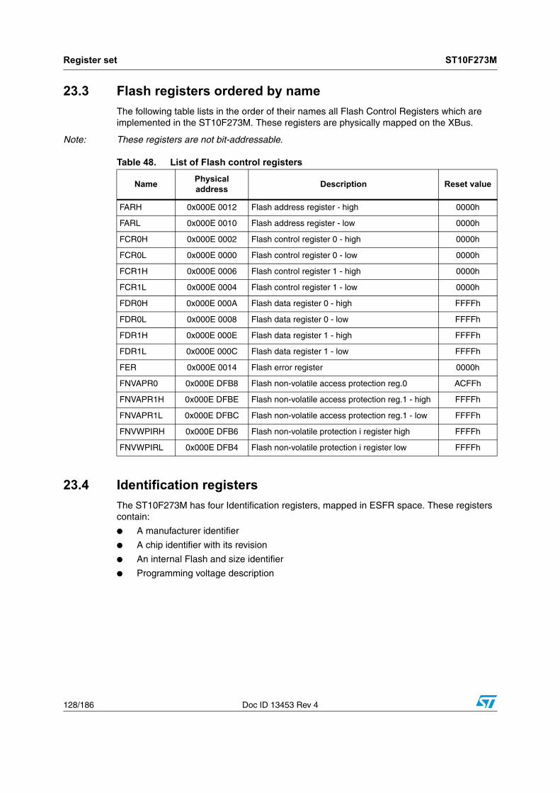
Register set ST10F273M
128/186 Doc ID 13453 Rev 4
23.3 Flash registers ordered by name
The following table lists in the order of their names all Flash Control Registers which are implemented in the ST10F273M. These registers are physically mapped on the XBus.
Note: These registers are not bit-addressable.
23.4 Identification registers
The ST10F273M has four Identification registers, mapped in ESFR space. These registers contain:
● A manufacturer identifier
● A chip identifier with its revision
● An internal Flash and size identifier
● Programming voltage description
Table 48. List of Flash control registers
NamePhysical address
Description Reset value
FARH 0x000E 0012 Flash address register - high 0000h
FARL 0x000E 0010 Flash address register - low 0000h
FCR0H 0x000E 0002 Flash control register 0 - high 0000h
FCR0L 0x000E 0000 Flash control register 0 - low 0000h
FCR1H 0x000E 0006 Flash control register 1 - high 0000h
FCR1L 0x000E 0004 Flash control register 1 - low 0000h
FDR0H 0x000E 000A Flash data register 0 - high FFFFh
FDR0L 0x000E 0008 Flash data register 0 - low FFFFh
FDR1H 0x000E 000E Flash data register 1 - high FFFFh
FDR1L 0x000E 000C Flash data register 1 - low FFFFh
FER 0x000E 0014 Flash error register 0000h
FNVAPR0 0x000E DFB8 Flash non-volatile access protection reg.0 ACFFh
FNVAPR1H 0x000E DFBE Flash non-volatile access protection reg.1 - high FFFFh
FNVAPR1L 0x000E DFBC Flash non-volatile access protection reg.1 - low FFFFh
FNVWPIRH 0x000E DFB6 Flash non-volatile protection i register high FFFFh
FNVWPIRL 0x000E DFB4 Flash non-volatile protection i register low FFFFh

ST10F273M Register set
Doc ID 13453 Rev 4 129/186
IDMANUF (F07Eh / 3Fh) ESFR Reset value: 0403h
15 14 13 12 11 10 9 8 7 6 5 4 3 2 1 0
MANUF 0 0 0 1 1
RO RO RO RO RO RO
Table 49. IDMANUF register description
Bit Name Function
15:5 MANUFManufacturer identifier
020h: STMicroelectronics manufacturer (JTAG worldwide normalization)
IDCHIP (F07Ch / 3Eh) ESFR Reset value: 111Xh
15 14 13 12 11 10 9 8 7 6 5 4 3 2 1 0
IDCHIP REVID
RO RO
Table 50. IDCHIP register description
Bit Name Function
15:4 IDCHIPDevice identifier
111h: ST10F273M identifier (273)
3:0 REVIDDevice revision identifier
Xh: According to revision number
IDMEM (F07Ah / 3Dh) ESFR Reset value: 2080h
15 14 13 12 11 10 9 8 7 6 5 4 3 2 1 0
MEMTYP MEMSIZE
RO RO
Table 51. IDMEM register description
Bit Name Function
15:12 MEMSIZEInternal memory size
Internal memory size is 4 x (MEMSIZE) (in Kbyte)080h for 512 Kbytes (ST10F273M)
11:0 MEMTYP
Internal memory type
0h: ROM-Less1h: (M) ROM memory2h: (S) Standard Flash memory (ST10F273M)3h: (H) High performance Flash memory4h...Fh: Reserved

Register set ST10F273M
130/186 Doc ID 13453 Rev 4
Note: All identification words are read-only registers.
IDPROG (F078h / 3Ch) ESFR Reset value: 0040h
15 14 13 12 11 10 9 8 7 6 5 4 3 2 1 0
PROGVPP PROGVDD
RO RO
Table 52. IDPROG register description
Bit Name Function
15:8 PROGVPP Programming VPP voltage (no need of external VPP) - 00h
7:0 PROGVDD
Programming VDD voltage
VDD voltage when programming EPROM or Flash devices is calculated using the following formula: VDD = 20 x [PROGVDD] / 256 (volts) - 40h for ST10F273M (5V).
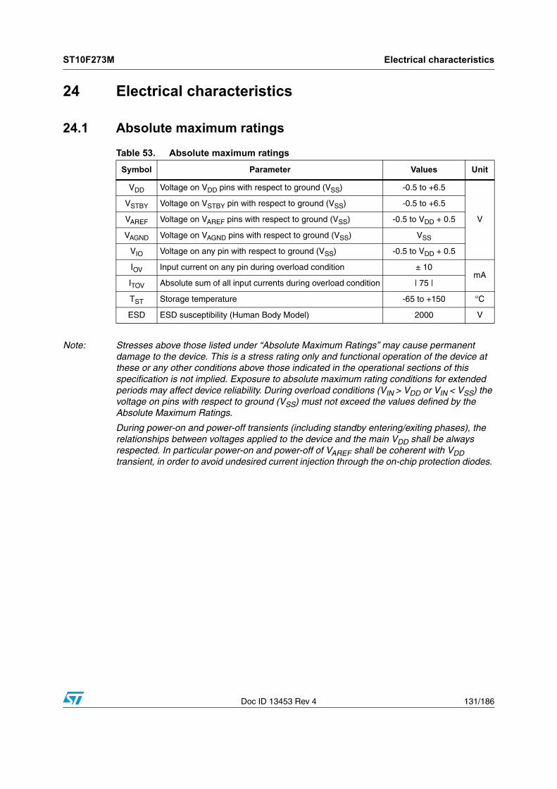
ST10F273M Electrical characteristics
Doc ID 13453 Rev 4 131/186
24 Electrical characteristics
24.1 Absolute maximum ratings
Note: Stresses above those listed under “Absolute Maximum Ratings” may cause permanent damage to the device. This is a stress rating only and functional operation of the device at these or any other conditions above those indicated in the operational sections of this specification is not implied. Exposure to absolute maximum rating conditions for extended periods may affect device reliability. During overload conditions (VIN > VDD or VIN < VSS) the voltage on pins with respect to ground (VSS) must not exceed the values defined by the Absolute Maximum Ratings.
During power-on and power-off transients (including standby entering/exiting phases), the relationships between voltages applied to the device and the main VDD shall be always respected. In particular power-on and power-off of VAREF shall be coherent with VDD transient, in order to avoid undesired current injection through the on-chip protection diodes.
Table 53. Absolute maximum ratings
Symbol Parameter Values Unit
VDD Voltage on VDD pins with respect to ground (VSS) -0.5 to +6.5
V
VSTBY Voltage on VSTBY pin with respect to ground (VSS) -0.5 to +6.5
VAREF Voltage on VAREF pins with respect to ground (VSS) -0.5 to VDD + 0.5
VAGND Voltage on VAGND pins with respect to ground (VSS) VSS
VIO Voltage on any pin with respect to ground (VSS) -0.5 to VDD + 0.5
IOV Input current on any pin during overload condition ± 10mA
ITOV Absolute sum of all input currents during overload condition | 75 |
TST Storage temperature -65 to +150 °C
ESD ESD susceptibility (Human Body Model) 2000 V

Electrical characteristics ST10F273M
132/186 Doc ID 13453 Rev 4
24.2 Recommended operating conditions
24.3 Power considerations
The average chip-junction temperature, TJ, in degrees Celsius, may be calculated using the following equation:
Equation 1:
TJ = TA + (PD x ΘJA)
Where:
TA is the Ambient Temperature in °C,
ΘJA is the Package Junction-to-Ambient Thermal Resistance, in °C/W,
PD is the sum of PINT and PI/O (PD = PINT + PI/O),
PINT is the product of IDD and VDD, expressed in Watt. This is the Chip Internal Power,
PI/O represents the Power Dissipation on Input and Output Pins; User Determined.
Most of the time for the applications PI/O< PINT and may be neglected. On the other hand, PI/O may be significant if the device is configured to drive continuously external modules and/or memories.
An approximate relationship between PD and TJ (if PI/O is neglected) is given by:
Equation 2:
PD = K / (TJ + 273°C)
Therefore (solving equations 1 and 2):
Equation 3:
K = PD x (TA + 273°C) + ΘJA x PD2
Table 54. Recommended operating conditions
Symbol ParameterValue
UnitMin Max
VDD Operating supply voltage4.5 5.5 V
VSTBY Operating standby supply voltage(1)
1. The value of the VSTBY voltage is specified in the range of 4.5 to 5.5 Volt. Nevertheless, it is acceptable to exceed the upper limit (up to 6.0 Volt) for a maximum of 100 hours over the global 300000 hours, representing the lifetime of the device (about 30 years). On the other hand, it is possible to exceed the lower limit (down to 4.0 Volt) whenever RTC and 32 kHz on-chip oscillator amplifier are turned off (only Standby RAM powered through VSTBY pin in Standby mode). When VSTBY voltage is lower than main VDD, the input section of VSTBY/EA pin can generate a spurious static consumption on VDD power supply (in the range of tenth of µA).
VAREF Operating analog reference voltage(2)
2. For details on operating conditions concerning the usage of A/D converter refer to Section 24.7.
0 VDD + 0.1
TA Ambient temperature under bias-40
+125°C
TJ Junction temperature under bias +150
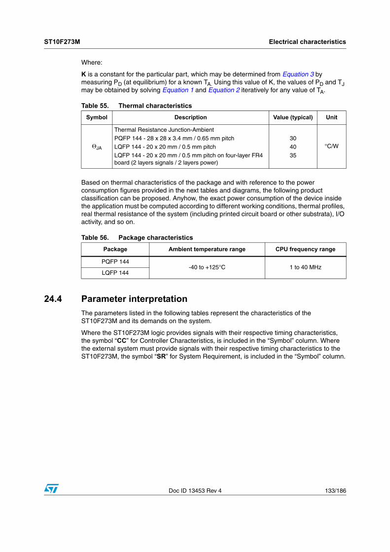
ST10F273M Electrical characteristics
Doc ID 13453 Rev 4 133/186
Where:
K is a constant for the particular part, which may be determined from Equation 3 by measuring PD (at equilibrium) for a known TA. Using this value of K, the values of PD and TJ may be obtained by solving Equation 1 and Equation 2 iteratively for any value of TA.
Based on thermal characteristics of the package and with reference to the power consumption figures provided in the next tables and diagrams, the following product classification can be proposed. Anyhow, the exact power consumption of the device inside the application must be computed according to different working conditions, thermal profiles, real thermal resistance of the system (including printed circuit board or other substrata), I/O activity, and so on.
24.4 Parameter interpretation
The parameters listed in the following tables represent the characteristics of the ST10F273M and its demands on the system.
Where the ST10F273M logic provides signals with their respective timing characteristics, the symbol “CC” for Controller Characteristics, is included in the “Symbol” column. Where the external system must provide signals with their respective timing characteristics to the ST10F273M, the symbol “SR” for System Requirement, is included in the “Symbol” column.
Table 55. Thermal characteristics
Symbol Description Value (typical) Unit
ΘJA
Thermal Resistance Junction-Ambient
PQFP 144 - 28 x 28 x 3.4 mm / 0.65 mm pitch
LQFP 144 - 20 x 20 mm / 0.5 mm pitchLQFP 144 - 20 x 20 mm / 0.5 mm pitch on four-layer FR4 board (2 layers signals / 2 layers power)
30
4035
°C/W
Table 56. Package characteristics
Package Ambient temperature range CPU frequency range
PQFP 144-40 to +125°C 1 to 40 MHz
LQFP 144

Electrical characteristics ST10F273M
134/186 Doc ID 13453 Rev 4
24.5 DC characteristics
VDD = 5 V ± 10%, VSS = 0 V, TA = -40 to +125°C
Table 57. DC characteristics
Symbol Parameter Test conditionLimit values
UnitMin Max
VIL SRInput low voltage (TTL mode)(except RSTIN, EA, NMI, RPD, XTAL1, READY)
– -0.3 0.8 V
VILS SRInput low voltage (CMOS mode)(except RSTIN, EA, NMI, RPD, XTAL1, READY)
– -0.3 0.3 VDD V
VIL1 SR Input low voltage RSTIN, EA, NMI, RPD – -0.3 0.3 VDD V
VIL2 SR Input low voltage XTAL1 (CMOS only) Direct drive mode -0.3 0.3 VDD V
VIL3 SR Input low voltage READY (TTL only) – -0.3 0.8 V
VIH SRInput high voltage (TTL mode)(except RSTIN, EA, NMI, RPD, XTAL1)
– 2.0 VDD + 0.3 V
VIHS SRInput high voltage (CMOS mode)(except RSTIN, EA, NMI, RPD, XTAL1)
– 0.7 VDD VDD + 0.3 V
VIH1 SR Input high voltage RSTIN, EA, NMI, RPD – 0.7 VDD VDD + 0.3 V
VIH2 SRInput high voltage XTAL1(CMOS only)
Direct drive mode 0.7 VDD VDD + 0.3 V
VIH3 SRInput high voltage READY (TTL only)
– 2.0 VDD + 0.3 V
VHYS CCInput hysteresis (TTL mode)(except RSTIN, EA, NMI, XTAL1, RPD)
(3) 400 700 mV
VHYSS CCInput hysteresis (CMOS mode)(except RSTIN, EA, NMI, XTAL1, RPD)
(3) 750 1400 mV
VHYS1 CC Input hysteresis RSTIN, EA, NMI (3) 750 1400 mV
VHYS2 CC Input hysteresis XTAL1 (3) 0 50 mV
VHYS3 CC Input hysteresis READY (TTL only) (3) 400 700 mV
VHYS4 CC Input hysteresis RPD (3) 500 1500 mV
VOL CCOutput low voltage(P6[7:0], ALE, RD, WR/WRL, BHE/WRH, CLKOUT, RSTIN, RSTOUT)
IOL = 8mAIOL = 1mA
–0.4
0.05V
VOL1 CCOutput low voltage(P0[15:0], P1[15:0], P2[15:0], P3[15,13:0], P4[7:0], P7[7:0], P8[7:0])
IOL1 = 4mAIOL1 = 0.5mA
–0.4
0.05V
VOL2 CC Output low voltage RPDIOL2 = 85µAIOL2 = 80µAIOL2 = 60µA
–VDD
0.5 VDD0.3 VDD
V
VOH CCOutput high voltage (P6[7:0], ALE, RD, WR/WRL, BHE/WRH, CLKOUT, RSTOUT)
IOH = -8mAIOH = -1mA
VDD - 0.8VDD -0.08
– V
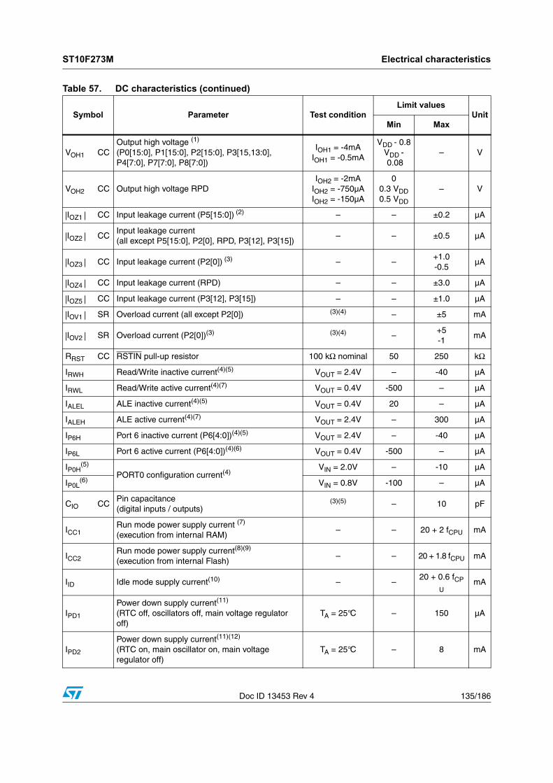
ST10F273M Electrical characteristics
Doc ID 13453 Rev 4 135/186
VOH1 CCOutput high voltage (1)
(P0[15:0], P1[15:0], P2[15:0], P3[15,13:0], P4[7:0], P7[7:0], P8[7:0])
IOH1 = -4mAIOH1 = -0.5mA
VDD - 0.8VDD -0.08
– V
VOH2 CC Output high voltage RPDIOH2 = -2mA
IOH2 = -750µAIOH2 = -150µA
00.3 VDD0.5 VDD
– V
|IOZ1 | CC Input leakage current (P5[15:0]) (2) – – ±0.2 µA
|IOZ2 | CCInput leakage current (all except P5[15:0], P2[0], RPD, P3[12], P3[15])
– – ±0.5 µA
|IOZ3 | CC Input leakage current (P2[0]) (3) – –+1.0-0.5
µA
|IOZ4 | CC Input leakage current (RPD) – – ±3.0 µA
|IOZ5 | CC Input leakage current (P3[12], P3[15]) – – ±1.0 µA
|IOV1 | SR Overload current (all except P2[0]) (3)(4) – ±5 mA
|IOV2 | SR Overload current (P2[0])(3) (3)(4) –+5-1
mA
RRST CC RSTIN pull-up resistor 100 kΩ nominal 50 250 kΩ
IRWH Read/Write inactive current(4)(5) VOUT = 2.4V – -40 µA
IRWL Read/Write active current(4)(7) VOUT = 0.4V -500 – µA
IALEL ALE inactive current(4)(5) VOUT = 0.4V 20 – µA
IALEH ALE active current(4)(7) VOUT = 2.4V – 300 µA
IP6H Port 6 inactive current (P6[4:0])(4)(5) VOUT = 2.4V – -40 µA
IP6L Port 6 active current (P6[4:0])(4)(6) VOUT = 0.4V -500 – µA
IP0H(5)
PORT0 configuration current(4)VIN = 2.0V – -10 µA
IP0L(6) VIN = 0.8V -100 – µA
CIO CCPin capacitance(digital inputs / outputs)
(3)(5) – 10 pF
ICC1Run mode power supply current (7)
(execution from internal RAM)– – 20 + 2 fCPU mA
ICC2Run mode power supply current(8)(9)
(execution from internal Flash)– – 20 + 1.8 fCPU mA
IID Idle mode supply current(10) – –20 + 0.6 fCP
UmA
IPD1
Power down supply current(11)
(RTC off, oscillators off, main voltage regulator off)
TA = 25°C – 150 µA
IPD2
Power down supply current(11)(12)
(RTC on, main oscillator on, main voltage regulator off)
TA = 25°C – 8 mA
Table 57. DC characteristics (continued)
Symbol Parameter Test conditionLimit values
UnitMin Max
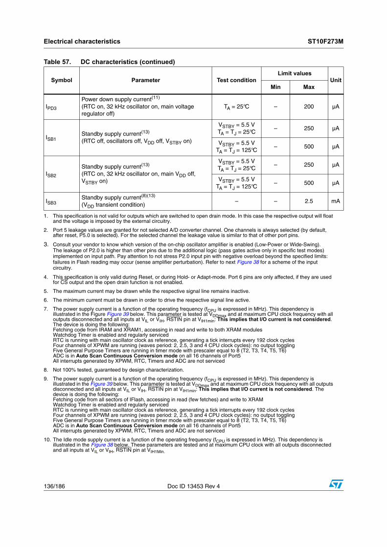
Electrical characteristics ST10F273M
136/186 Doc ID 13453 Rev 4
IPD3
Power down supply current(11)
(RTC on, 32 kHz oscillator on, main voltage regulator off)
TA = 25°C – 200 µA
ISB1Standby supply current(13)
(RTC off, oscillators off, VDD off, VSTBY on)
VSTBY = 5.5 V
TA = TJ = 25°C– 250 µA
VSTBY = 5.5 V
TA = TJ = 125°C– 500 µA
ISB2
Standby supply current(13)
(RTC on, 32 kHz oscillator on, main VDD off, VSTBY on)
VSTBY = 5.5 VTA = TJ = 25°C
– 250 µA
VSTBY = 5.5 VTA = TJ = 125°C
– 500 µA
ISB3Standby supply current(8)(13)
(VDD transient condition)– – 2.5 mA
1. This specification is not valid for outputs which are switched to open drain mode. In this case the respective output will float and the voltage is imposed by the external circuitry.
2. Port 5 leakage values are granted for not selected A/D converter channel. One channels is always selected (by default, after reset, P5.0 is selected). For the selected channel the leakage value is similar to that of other port pins.
3. Consult your vendor to know which version of the on-chip oscillator amplifier is enabled (Low-Power or Wide-Swing).The leakage of P2.0 is higher than other pins due to the additional logic (pass gates active only in specific test modes) implemented on input path. Pay attention to not stress P2.0 input pin with negative overload beyond the specified limits: failures in Flash reading may occur (sense amplifier perturbation). Refer to next Figure 38 for a scheme of the input circuitry.
4. This specification is only valid during Reset, or during Hold- or Adapt-mode. Port 6 pins are only affected, if they are used for CS output and the open drain function is not enabled.
5. The maximum current may be drawn while the respective signal line remains inactive.
6. The minimum current must be drawn in order to drive the respective signal line active.
7. The power supply current is a function of the operating frequency (fCPU is expressed in MHz). This dependency is illustrated in the Figure Figure 39 below. This parameter is tested at VDDmax and at maximum CPU clock frequency with all outputs disconnected and all inputs at VIL or VIH, RSTIN pin at VIH1min: This implies that I/O current is not considered. The device is doing the following: Fetching code from IRAM and XRAM1, accessing in read and write to both XRAM modulesWatchdog Timer is enabled and regularly servicedRTC is running with main oscillator clock as reference, generating a tick interrupts every 192 clock cyclesFour channels of XPWM are running (waves period: 2, 2.5, 3 and 4 CPU clock cycles): no output togglingFive General Purpose Timers are running in timer mode with prescaler equal to 8 (T2, T3, T4, T5, T6)ADC is in Auto Scan Continuous Conversion mode on all 16 channels of Port5All interrupts generated by XPWM, RTC, Timers and ADC are not serviced
8. Not 100% tested, guaranteed by design characterization.
9. The power supply current is a function of the operating frequency (fCPU is expressed in MHz). This dependency is illustrated in the Figure 39 below. This parameter is tested at VDDmax and at maximum CPU clock frequency with all outputs disconnected and all inputs at VIL or VIH, RSTIN pin at VIH1min: This implies that I/O current is not considered. The device is doing the following: Fetching code from all sectors of IFlash, accessing in read (few fetches) and write to XRAMWatchdog Timer is enabled and regularly servicedRTC is running with main oscillator clock as reference, generating a tick interrupts every 192 clock cyclesFour channels of XPWM are running (waves period: 2, 2.5, 3 and 4 CPU clock cycles): no output togglingFive General Purpose Timers are running in timer mode with prescaler equal to 8 (T2, T3, T4, T5, T6)ADC is in Auto Scan Continuous Conversion mode on all 16 channels of Port5All interrupts generated by XPWM, RTC, Timers and ADC are not serviced
10. The Idle mode supply current is a function of the operating frequency (fCPU is expressed in MHz). This dependency is illustrated in the Figure 38 below. These parameters are tested and at maximum CPU clock with all outputs disconnected and all inputs at VIL or VIH, RSTIN pin at VIH1Min.
Table 57. DC characteristics (continued)
Symbol Parameter Test conditionLimit values
UnitMin Max

ST10F273M Electrical characteristics
Doc ID 13453 Rev 4 137/186
Figure 38. Port2 test mode structure
Figure 39. Supply current versus the operating frequency (RUN and IDLE modes)
11. This parameter is tested including leakage currents. All inputs (including pins configured as inputs) at 0 V to 0.1 V or at VDD – 0.1 V to VDD, VAREF = 0 V, all outputs (including pins configured as outputs) disconnected. Besides, the Main Voltage Regulator is assumed off: in case it is not, additional 1mA shall be assumed. The value for this parameter shall be considered as “Target Value” to be confirmed by silicon characterization.
12. Overload conditions occur if the standard operating conditions are exceeded, that is, the voltage on any pin exceeds the specified range (that is, VOV > VDD + 0.3 V or VOV < –0.3 V). The absolute sum of input overload currents on all port pins may not exceed 50mA. The supply voltage must remain within the specified limits.
13. This parameter is tested including leakage currents. All inputs (including pins configured as inputs) at 0 V to 0.1 V or at VDD – 0.1 V to VDD, VAREF = 0 V, all outputs (including pins configured as outputs) disconnected. Besides, the Main Voltage Regulator is assumed off: in case it is not, additional 1mA shall be assumed. The value for this parameter shall be considered as “Target Value” to be confirmed by silicon characterization.
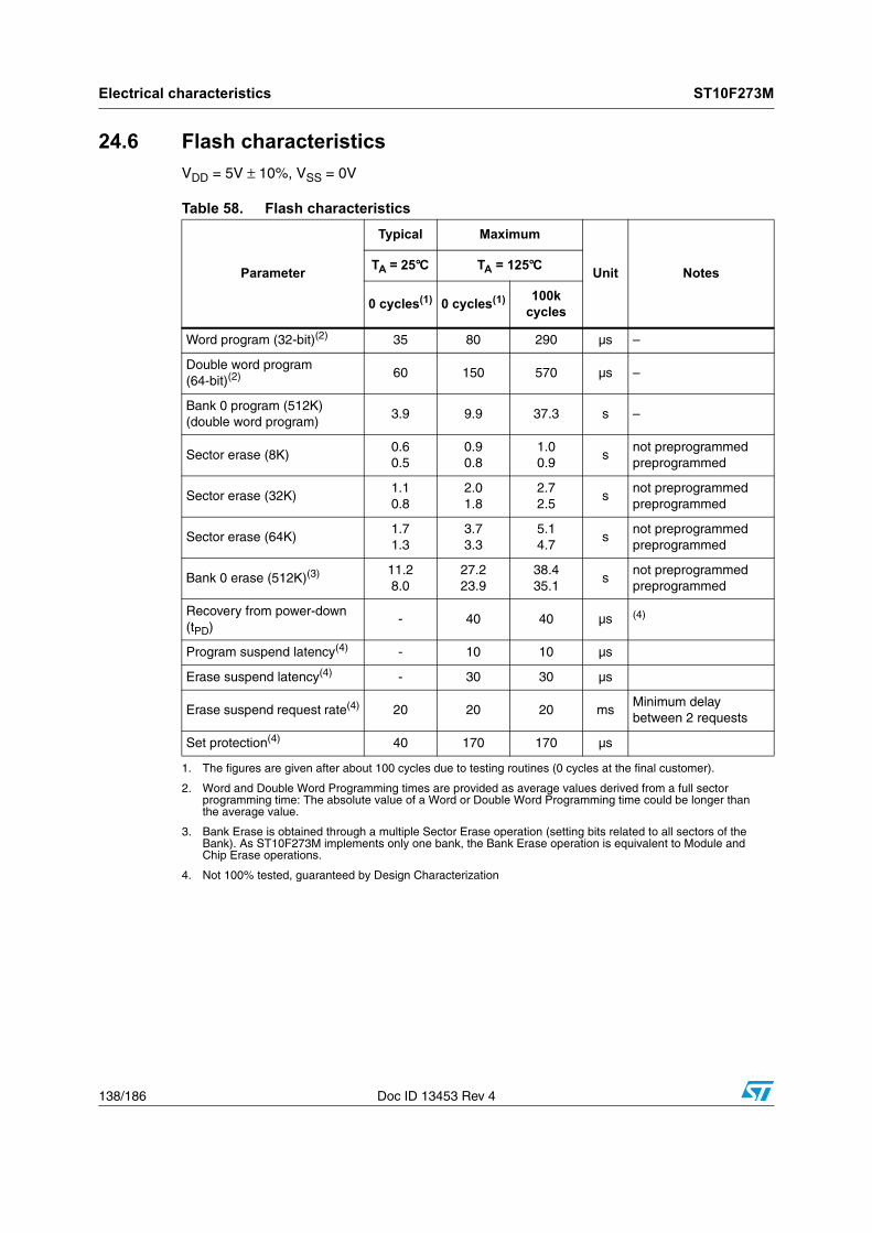
Electrical characteristics ST10F273M
138/186 Doc ID 13453 Rev 4
24.6 Flash characteristics
VDD = 5V ± 10%, VSS = 0V
Table 58. Flash characteristics
Parameter
Typical Maximum
Unit NotesTA = 25°C TA = 125°C
0 cycles(1)
1. The figures are given after about 100 cycles due to testing routines (0 cycles at the final customer).
0 cycles(1) 100k cycles
Word program (32-bit)(2)
2. Word and Double Word Programming times are provided as average values derived from a full sector programming time: The absolute value of a Word or Double Word Programming time could be longer than the average value.
35 80 290 µs –
Double word program (64-bit)(2) 60 150 570 µs –
Bank 0 program (512K)(double word program)
3.9 9.9 37.3 s –
Sector erase (8K)0.60.5
0.90.8
1.00.9
snot preprogrammedpreprogrammed
Sector erase (32K)1.10.8
2.01.8
2.72.5
snot preprogrammedpreprogrammed
Sector erase (64K)1.71.3
3.73.3
5.14.7
snot preprogrammedpreprogrammed
Bank 0 erase (512K)(3)
3. Bank Erase is obtained through a multiple Sector Erase operation (setting bits related to all sectors of the Bank). As ST10F273M implements only one bank, the Bank Erase operation is equivalent to Module and Chip Erase operations.
11.28.0
27.223.9
38.435.1
snot preprogrammedpreprogrammed
Recovery from power-down (tPD)
- 40 40 µs (4)
4. Not 100% tested, guaranteed by Design Characterization
Program suspend latency(4) - 10 10 µs
Erase suspend latency(4) - 30 30 µs
Erase suspend request rate(4) 20 20 20 msMinimum delay between 2 requests
Set protection(4) 40 170 170 µs

ST10F273M Electrical characteristics
Doc ID 13453 Rev 4 139/186
24.7 A/D converter characteristics
VDD = 5V ± 10%, VSS = 0V, TA = -40 to +125°C, 4.5V ≤ VAREF ≤ VDD, VSS ≤ VAGND ≤ VSS + 0.2V
Table 59. Flash data retention characteristics
Number of program / erase cycles
(-40°C < TA < 125°C)
Data retention time(average ambient temperature 60°C)
256 Kbyte (code store)64 Kbyte
(EEPROM emulation)(1)
1. Two 64 Kbyte Flash Sectors may be typically used to emulate up to 4, 8 or 16 Kbytes of EEPROM.Therefore, in case of an emulation of a 16 Kbyte EEPROM, 100,000 Flash Program / Erase cycles are equivalent to 800,000 EEPROM Program/Erase cycles.For an efficient use of the Read While Write feature and/or EEPROM Emulation, please refer to the dedicated application note EEPROM Emulation with ST10F2xx (AN2061). Contact your local field service, local sales person or STMicroelectronics representative to obtain a copy of such a guideline document.
0 - 100 > 20 years > 20 years
1000 - > 20 years
10000 - 10 years
100000 - 1 year
Table 60. A/D converter characteristics
Symbol Parameter Test conditionLimit values
UnitMin Max
VAREF SR Analog reference voltage(1) 4.5 VDD V
VAGND SR Analog ground voltage VSS VSS + 0.2 V
VAIN SR Analog input voltage(2) VAGND VAREF V
IAREF CC Reference supply currentRunning mode(3) – 5 mA
Power down mode – 1 µA
tS CC Sample time (4) 1 – µs
tC CC Conversion time (5) 3 – µs
DNL CC Differential non linearity(6) No overload –1 +1 LSB
INL CC Integral non linearity(6) No overload –1.5 +1.5 LSB
OFS CC Offset error(6) No overload –1.5 +1.5 LSB
TUE CC Total unadjusted error(6)Port5Port1 - No overload(3)
Port1 - Overload(3)
–2.0–5.0–7.0
+2.0+5.0+7.0
LSB
K CCCoupling factor between inputs(3)(7)
On both Port5 and Port1
– 10–6 –
CP1 CC
Input pin capacitance(3)(8)– 3 pF
CP2 CCPort5Port1
–46
pF

Electrical characteristics ST10F273M
140/186 Doc ID 13453 Rev 4
24.7.1 Conversion timing control
When a conversion is started, first the capacitances of the converter are loaded via the respective analog input pin to the current analog input voltage. The time to load the capacitances is referred to as sample time. Next the sampled voltage is converted to a digital value several successive steps, which correspond to the 10-bit resolution of the ADC. During these steps the internal capacitances are repeatedly charged and discharged via the VAREF pin.
The current that has to be drawn from the sources for sampling and changing charges depends on the time that each respective step takes, because the capacitors must reach their final voltage level within the given time, at least with a certain approximation. The maximum current, however, that a source can deliver, depends on its internal resistance.
The time that the two different actions (sampling, and converting) take during conversion can be programmed within a certain range in the ST10F273M relative to the CPU clock. The absolute time that is consumed by the different conversion steps therefore is independent
CS CC Sampling capacitance(3)(8) – 3.5 pF
RSW CCAnalog switch resistance(3)(8)
Port5Port1
––
6001600
Ω
RAD CC – 1300 Ω
1. VAREF can be tied to ground when A/D converter is not in use: An extra consumption (around 200µA) on main VDD is added due to internal analog circuitry not completely turned off. Therefore, it is suggested to maintain the VAREF at VDD level even when not in use, and eventually switch off the A/D converter circuitry by setting bit ADOFF in ADCON register.
2. VAIN may exceed VAGND or VAREF up to the absolute maximum ratings. However, the conversion result in these cases will be 0x000H or 0x3FFH, respectively.
3. Not 100% tested, guaranteed by design characterization.
4. During the sample time the input capacitance CAIN can be charged/discharged by the external source. The internal resistance of the analog source must allow the capacitance to reach its final voltage level within tS. After the end of the sample time tS, changes of the analog input voltage have no effect on the conversion result.Values for the sample clock tS depends on programming and can be taken from Table 61: A/D converter programming.
5. This parameter includes the sample time tS, the time for determining the digital result and the time to load the result register with the conversion result. Values for the conversion clock tCC depend on programming and can be taken from next Table 61.
6. DNL, INL, OFS and TUE are tested at VAREF = 5.0 V, VAGND = 0V, VDD = 5.0 V. It is guaranteed by design characterization for all other voltages within the defined voltage range.‘LSB’ has a value of VAREF/1024. For Port5 channels, the specified TUE (± 2LSB) is guaranteed also with an overload condition (see IOV specification) occurring on maximum 2 not selected analog input pins of Port5 and if the absolute sum of input overload currents on all Port5 analog input pins does not exceed 10 mA. For Port1 channels, the specified TUE is guaranteed when no overload condition is applied to Port1 pins: When an overload condition occurs on maximum 2 not selected analog input pins of Port1 and the input positive overload current on all analog input pins does not exceed 10 mA (either dynamic or static injection), the specified TUE is degraded (± 7LSB). To acheive the same accuracy, the negative injection current on Port1 pins must not exceed -1mA in case of both dynamic and static injection.
7. The coupling factor is measured on a channel while an overload condition occurs on the adjacent not selected channels with the overload current within the different specified ranges (for both positive and negative injection current).
8. Refer to scheme in Figure 41.
Table 60. A/D converter characteristics (continued)
Symbol Parameter Test conditionLimit values
UnitMin Max
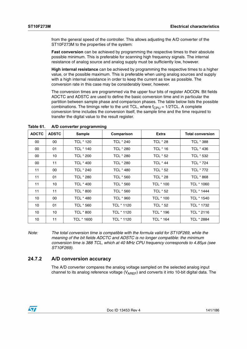
ST10F273M Electrical characteristics
Doc ID 13453 Rev 4 141/186
from the general speed of the controller. This allows adjusting the A/D converter of the ST10F273M to the properties of the system:
Fast conversion can be achieved by programming the respective times to their absolute possible minimum. This is preferable for scanning high frequency signals. The internal resistance of analog source and analog supply must be sufficiently low, however.
High internal resistance can be achieved by programming the respective times to a higher value, or the possible maximum. This is preferable when using analog sources and supply with a high internal resistance in order to keep the current as low as possible. The conversion rate in this case may be considerably lower, however.
The conversion times are programmed via the upper four bits of register ADCON. Bit fields ADCTC and ADSTC are used to define the basic conversion time and in particular the partition between sample phase and comparison phases. The table below lists the possible combinations. The timings refer to the unit TCL, where fCPU = 1/2TCL. A complete conversion time includes the conversion itself, the sample time and the time required to transfer the digital value to the result register.
Note: The total conversion time is compatible with the formula valid for ST10F269, while the meaning of the bit fields ADCTC and ADSTC is no longer compatible: the minimum conversion time is 388 TCL, which at 40 MHz CPU frequency corresponds to 4.85µs (see ST10F269).
24.7.2 A/D conversion accuracy
The A/D converter compares the analog voltage sampled on the selected analog input channel to its analog reference voltage (VAREF) and converts it into 10-bit digital data. The
Table 61. A/D converter programming
ADCTC ADSTC Sample Comparison Extra Total conversion
00 00 TCL * 120 TCL * 240 TCL * 28 TCL * 388
00 01 TCL * 140 TCL * 280 TCL * 16 TCL * 436
00 10 TCL * 200 TCL * 280 TCL * 52 TCL * 532
00 11 TCL * 400 TCL * 280 TCL * 44 TCL * 724
11 00 TCL * 240 TCL * 480 TCL * 52 TCL * 772
11 01 TCL * 280 TCL * 560 TCL * 28 TCL * 868
11 10 TCL * 400 TCL * 560 TCL * 100 TCL * 1060
11 11 TCL * 800 TCL * 560 TCL * 52 TCL * 1444
10 00 TCL * 480 TCL * 960 TCL * 100 TCL * 1540
10 01 TCL * 560 TCL * 1120 TCL * 52 TCL * 1732
10 10 TCL * 800 TCL * 1120 TCL * 196 TCL * 2116
10 11 TCL * 1600 TCL * 1120 TCL * 164 TCL * 2884

Electrical characteristics ST10F273M
142/186 Doc ID 13453 Rev 4
absolute accuracy of the A/D conversion is the deviation between the input analog value and the output digital value. It includes the following errors:
● Offset error (OFS)
● Gain error (GE)
● Quantization error
● Non-linearity error (Differential and Integral)
These four error quantities are explained below using Figure 40.
Offset error
Offset error is the deviation between actual and ideal A/D conversion characteristics when the digital output value changes from the minimum (zero voltage) 00 to 01 (Figure 40, see OFS).
Gain error
Gain error is the deviation between the actual and ideal A/D conversion characteristics when the digital output value changes from the 3FEh to the maximum 3FFh once offset error is subtracted. Gain error combined with offset error represents the so-called full-scale error (Figure 40, OFS + GE).
Quantization error
Quantization error is the intrinsic error of the A/D converter and is expressed as 1/2 LSB.
Non-linearity error
Non-linearity error is the deviation between actual and the best-fitting A/D conversion characteristics (see Figure 40):
● Differential non-linearity error is the actual step dimension versus the ideal one (1 LSBIDEAL).
● Integral non-linearity error is the distance between the center of the actual step and the center of the bisector line, in the actual characteristics. Note that for integral non-linearity error, the effect of offset, gain and quantization errors is not included.
Note: Bisector characteristic is obtained drawing a line from 1/2 LSB before the first step of the real characteristic, and 1/2 LSB after the last step again of the real characteristic.
24.7.3 Total unadjusted error
The total unadjusted error specifies the maximum deviation from the ideal characteristic: The number provided in the datasheet represents the maximum error with respect to the entire characteristic. It is a combination of the offset, gain and integral linearity errors. The different errors may compensate each other depending on the relative sign of the offset and gain errors. Refer to Figure 40, see TUE.
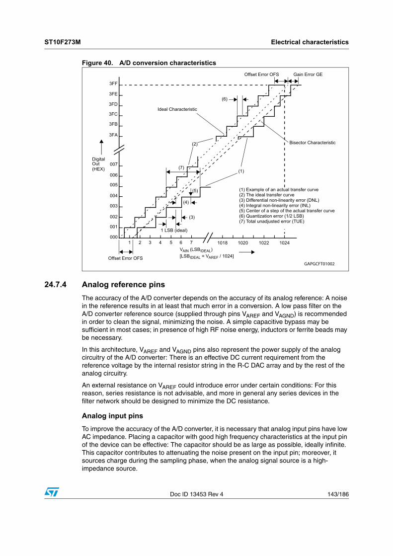
ST10F273M Electrical characteristics
Doc ID 13453 Rev 4 143/186
Figure 40. A/D conversion characteristics
24.7.4 Analog reference pins
The accuracy of the A/D converter depends on the accuracy of its analog reference: A noise in the reference results in at least that much error in a conversion. A low pass filter on the A/D converter reference source (supplied through pins VAREF and VAGND) is recommended in order to clean the signal, minimizing the noise. A simple capacitive bypass may be sufficient in most cases; in presence of high RF noise energy, inductors or ferrite beads may be necessary.
In this architecture, VAREF and VAGND pins also represent the power supply of the analog circuitry of the A/D converter: There is an effective DC current requirement from the reference voltage by the internal resistor string in the R-C DAC array and by the rest of the analog circuitry.
An external resistance on VAREF could introduce error under certain conditions: For this reason, series resistance is not advisable, and more in general any series devices in the filter network should be designed to minimize the DC resistance.
Analog input pins
To improve the accuracy of the A/D converter, it is necessary that analog input pins have low AC impedance. Placing a capacitor with good high frequency characteristics at the input pin of the device can be effective: The capacitor should be as large as possible, ideally infinite. This capacitor contributes to attenuating the noise present on the input pin; moreover, it sources charge during the sampling phase, when the analog signal source is a high-impedance source.

Electrical characteristics ST10F273M
144/186 Doc ID 13453 Rev 4
A real filter can typically be obtained by using a series resistance with a capacitor on the input pin (simple RC Filter). The RC filtering may be limited according to the value of source impedance of the transducer or circuit supplying the analog signal to be measured. The filter at the input pins must be designed taking into account the dynamic characteristics of the input signal (bandwidth).
Figure 41. A/D converter input pins scheme
Input leakage and external circuit
The series resistor utilized to limit the current to a pin (see RL in Figure 41), in combination with a large source impedance, can lead to a degradation of A/D converter accuracy when input leakage is present.
Data about maximum input leakage current at each pin is provided in the datasheet (Electrical characteristics section). Input leakage is greatest at high operating temperatures and in general decreases by one half for each 10° C decrease in temperature.
Considering that, for a 10-bit A/D converter one count is about 5mV (assuming VAREF = 5V), an input leakage of 100nA acting though an RL = 50kΩ of external resistance leads to an error of exactly one count (5mV); if the resistance were 100kΩ, the error would become two counts.
Eventual additional leakage due to external clamping diodes must also be taken into account in computing the total leakage affecting the A/D converter measurements. Another contribution to the total leakage is represented by the charge-sharing effects with the sampling capacitance: CS being substantially a switched capacitance, with a frequency equal to the conversion rate of a single channel (maximum when fixed channel continuous conversion mode is selected), it can be seen as a resistive path to ground. For instance, assuming a conversion rate of 250 kHz, with CS equal to 4pF, a resistance of 1MΩ is obtained (REQ = 1 / fCCS, where fC represents the conversion rate at the considered channel). To minimize the error induced by the voltage partitioning between this resistance
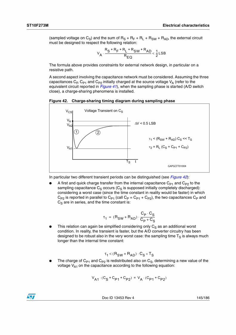
ST10F273M Electrical characteristics
Doc ID 13453 Rev 4 145/186
(sampled voltage on CS) and the sum of RS + RF + RL + RSW + RAD, the external circuit must be designed to respect the following relation:
The formula above provides constraints for external network design, in particular on a resistive path.
A second aspect involving the capacitance network must be considered. Assuming the three capacitances CF, CP1 and CP2 initially charged at the source voltage VA (refer to the equivalent circuit reported in Figure 41), when the sampling phase is started (A/D switch close), a charge-sharing phenomena is installed.
Figure 42. Charge-sharing timing diagram during sampling phase
In particular two different transient periods can be distinguished (see Figure 42):
● A first and quick charge transfer from the internal capacitance CP1 and CP2 to the sampling capacitance CS occurs (CS is supposed initially completely discharged): considering a worst case (since the time constant in reality would be faster) in which CP2 is reported in parallel to CP1 (call CP = CP1 + CP2), the two capacitances CP and CS are in series, and the time constant is:
● This relation can again be simplified considering only CS as an additional worst condition. In reality, the transient is faster, but the A/D converter circuitry has been designed to be robust also in the very worst case: the sampling time TS is always much longer than the internal time constant:
● The charge of CP1 and CP2 is redistributed also on CS, determining a new value of the voltage VA1 on the capacitance according to the following equation:
VA
RS RF RL RSW RAD+ + + +
REQ------------------------------------------------------------------------------⋅ 1
2--- LSB<
τ1 RSW RAD+( )CP CS⋅CP CS+----------------------⋅=
τ1 RSW RAD+( ) CS TS«⋅<
VA1 CS CP1 CP2+ +( )⋅ VA CP1 CP2+( )⋅=
Electrical characteristics ST10F273M
146/186 Doc ID 13453 Rev 4
● A second charge transfer involves also CF (that is typically bigger than the on-chip capacitance) through the resistance RL: again considering the worst case in which CP2 and CS were in parallel to CP1 (since the time constant in reality would be faster), the time constant is:
● In this case, the time constant depends on the external circuit: in particular imposing that the transient is completed well before the end of sampling time TS, a constraint on RL sizing is obtained:
● Of course, RL shall be sized also according to the current limitation constraints, in combination with RS (source impedance) and RF (filter resistance). CF being definitively bigger than CP1, CP2 and CS, the final voltage VA2 (at the end of the charge transfer transient) will then be much higher than VA1. The following equation must be respected (charge balance assuming now CS already charged at VA1):
The two transients above are not influenced by the voltage source that, due to the presence of the RFCF filter, is not able to provide the extra charge to compensate the voltage drop on CS with respect to the ideal source VA; the time constant RFCF of the filter is very high with respect to the sampling time (TS). The filter is typically designed to act as anti-aliasing (see Figure 43).
Calling f0 the bandwidth of the source signal (and as a consequence the cut-off frequency of the anti-aliasing filter, fF), according to Nyquist theorem the conversion rate fC must be at least 2f0; it means that the constant time of the filter is greater than or at least equal to twice the conversion period (TC). Again the conversion period TC is longer than the sampling time TS, which is just a portion of it, even when fixed channel continuous conversion mode is selected (fastest conversion rate at a specific channel): In conclusion it is evident that the time constant of the filter RFCF is definitively much higher than the sampling time TS, so the charge level on CS cannot be modified by the analog signal source during the time in which the sampling switch is closed.
τ2 RL< CS CP1 CP2+ +( )⋅
10 τ2⋅ 10 R⋅ L= CS CP1 CP2+ +( ) TS≤⋅
VA2 CS CP1 CP2 CF+ + +( )⋅ VA CF⋅ VA1+ CP1 CP2+ CS+( )⋅=
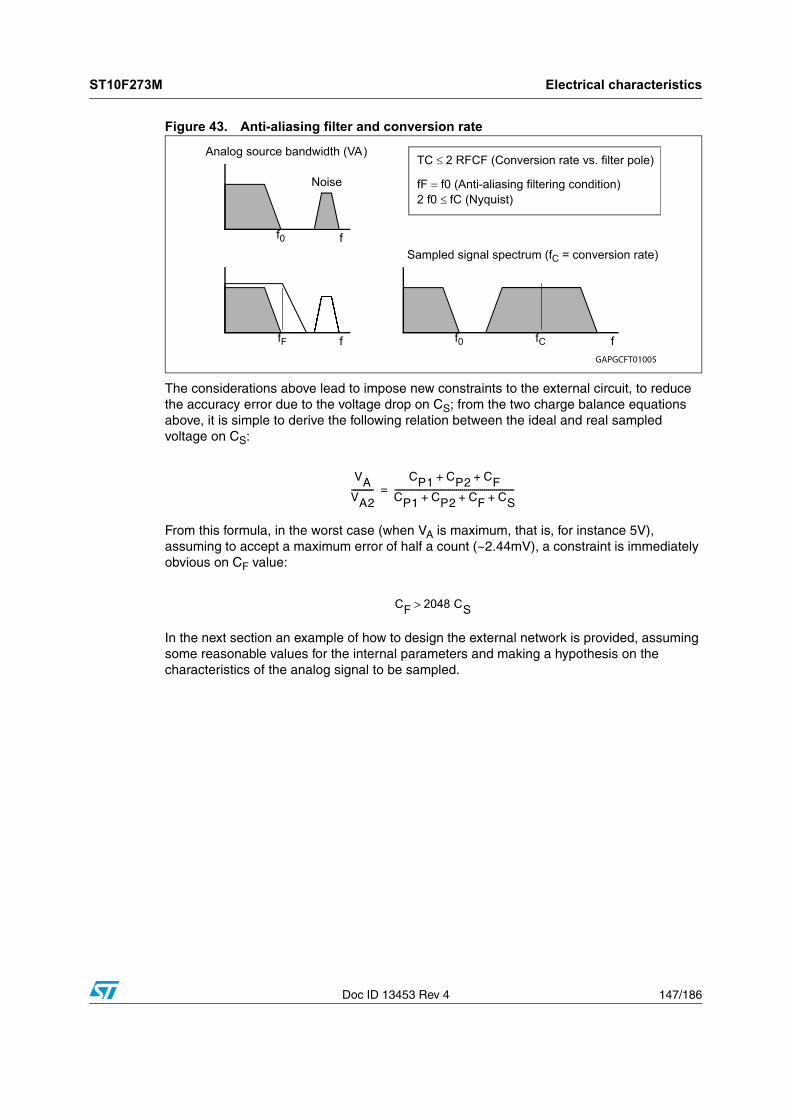
ST10F273M Electrical characteristics
Doc ID 13453 Rev 4 147/186
Figure 43. Anti-aliasing filter and conversion rate
The considerations above lead to impose new constraints to the external circuit, to reduce the accuracy error due to the voltage drop on CS; from the two charge balance equations above, it is simple to derive the following relation between the ideal and real sampled voltage on CS:
From this formula, in the worst case (when VA is maximum, that is, for instance 5V), assuming to accept a maximum error of half a count (~2.44mV), a constraint is immediately obvious on CF value:
In the next section an example of how to design the external network is provided, assuming some reasonable values for the internal parameters and making a hypothesis on the characteristics of the analog signal to be sampled.
VAVA2-----------
CP1 CP2+ CF+
CP1 CP2+ CF CS+ +------------------------------------------------------------=
CF 2048 CS⋅>
Electrical characteristics ST10F273M
148/186 Doc ID 13453 Rev 4
Example of external network sizing
The following hypotheses are formulated in order to proceed in designing the external network on A/D converter input pins:
● Analog Signal Source Bandwidth (f0): 10 kHz
● Conversion Rate (fC): 25 kHz
● Sampling Time (TS): 1µs
● Pin Input Capacitance (CP1): 5pF
● Pin Input Routing Capacitance (CP2): 1pF
● Sampling Capacitance (CS): 4pF
● Maximum Input Current Injection (IINJ): 3mA
● Maximum Analog Source Voltage (VAM): 12V
● Analog Source Impedance (RS): 100Ω● Channel Switch Resistance (RSW): 500Ω● Sampling Switch Resistance (RAD): 200Ω
1. Supposing to design the filter with the pole exactly at the maximum frequency of the signal, the time constant of the filter is:
2. Using the relation between CF and CS and taking some margin (4000 instead of 2048), it is possible to define CF:
3. As a consequence of step 1 and 2, RC can be chosen:
4. Considering the current injection limitation and supposing that the source can go up to 12V, the total series resistance can be defined as:
from which is now simple to define the value of RL:
5. Now the three elements of the external circuit RF, CF and RL are defined. Some conditions discussed in the previous paragraphs have been used to size the component, the other must now be verified. The relation which allows minimization of
RCCF1
2πf0------------ 15.9μs==
CF 4000 CS⋅ 16nF==
RF1
2πf0CF--------------------- 995Ω 1kΩ≅==
RS RF RL
VAMIINJ------------- 4kΩ==+ +
RL
VAMIINJ------------- RF RS 2.9kΩ=––=

ST10F273M Electrical characteristics
Doc ID 13453 Rev 4 149/186
the accuracy error introduced by the switched capacitance equivalent resistance is in this case:
So the error due to the voltage partitioning between the real resistive path and CS is less then half a count (considering the worst case when VA = 5V):
The other condition to be verified is if the time constants of the transients are really and significantly shorter than the sampling period duration TS:
For the complete set of parameters characterizing the ST10F273M A/D converter equivalent circuit, refer to Section 24.7: A/D converter characteristics on page 139.
24.8 AC characteristics
24.8.1 Test waveforms
Figure 44. Input/output waveforms
REQ1
fCCS--------------- 10MΩ==
VA
RS RF RL RSW RAD+ + + +
REQ--------------------------------------------------------------------------- 2.35mV=⋅ 1
2---LSB<
τ1 RSW RAD+( )= CS 2.8ns=⋅ TS = 1μs
10 τ2⋅ 10 R⋅ L= CS CP1 CP2+ +( ) 290ns=⋅ TS = 1μs
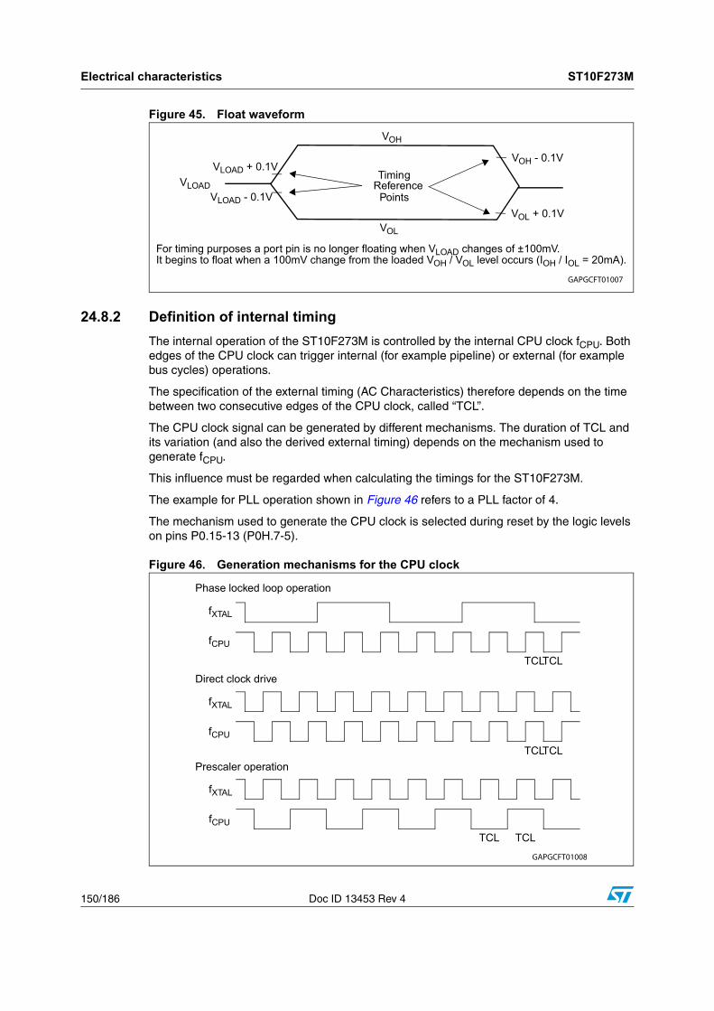
Electrical characteristics ST10F273M
150/186 Doc ID 13453 Rev 4
Figure 45. Float waveform
24.8.2 Definition of internal timing
The internal operation of the ST10F273M is controlled by the internal CPU clock fCPU. Both edges of the CPU clock can trigger internal (for example pipeline) or external (for example bus cycles) operations.
The specification of the external timing (AC Characteristics) therefore depends on the time between two consecutive edges of the CPU clock, called “TCL”.
The CPU clock signal can be generated by different mechanisms. The duration of TCL and its variation (and also the derived external timing) depends on the mechanism used to generate fCPU.
This influence must be regarded when calculating the timings for the ST10F273M.
The example for PLL operation shown in Figure 46 refers to a PLL factor of 4.
The mechanism used to generate the CPU clock is selected during reset by the logic levels on pins P0.15-13 (P0H.7-5).
Figure 46. Generation mechanisms for the CPU clock

ST10F273M Electrical characteristics
Doc ID 13453 Rev 4 151/186
24.8.3 Clock generation modes
The next Table 62 associates the combinations of these three bits with the respective clock generation mode.
24.8.4 Prescaler operation
When pins P0.15-13 (P0H.7-5) equal ‘001’ during reset, the CPU clock is derived from the internal oscillator (input clock signal) by a 2:1 prescaler.
The frequency of fCPU is half the frequency of fXTAL and the high and low time of fCPU (that is, the duration of an individual TCL) is defined by the period of the input clock fXTAL.
The timings listed in the AC Characteristics that refer to TCL therefore can be calculated using the period of fXTAL for any TCL.
Note that if the bit OWDDIS in SYSCON register is cleared, the PLL runs on its free-running frequency and delivers the clock signal for the Oscillator Watchdog. If bit OWDDIS is set, then the PLL is switched off.
24.8.5 Direct drive
When pins P0.15-13 (P0H.7-5) equal ‘011’ during reset the on-chip phase locked loop is disabled, the on-chip oscillator amplifier is bypassed and the CPU clock is directly driven by the input clock signal on XTAL1 pin.
Table 62. On-chip clock generator selections
P0.15-13(P0H.7-5)
CPU frequency fCPU = fXTAL x F
External clock input range(1)(2)
1. The external clock input range refers to a CPU clock range of 1...40 MHz. Moreover, the PLL usage is limited to 4 to 12 MHz input frequency range. All configurations need a crystal (or ceramic resonator) to generate the CPU clock through the internal oscillator amplifier (apart from Direct Drive): vice versa, the clock can be forced through an external clock source only in Direct Drive mode (on-chip oscillator amplifier disabled, so no crystal or resonator can be used).
2. The limits on input frequency are 4 to 12 MHz since the usage of the internal oscillator amplifier is required. Also when the PLL is not used and the CPU clock corresponds to fXTAL/2, an external crystal or resonator shall be used: it is not possible to force any clock though an external clock source.
NotesMain OSC (MHz)
1 1 1 fXTAL x 4 4 to 8 Default configuration
1 1 0 fXTAL x 3 5.3 to 10.6
1 0 1 fXTAL x 8 4 to 5
1 0 0 fXTAL x 5 6.4 to 8
0 1 1 fXTAL x 1 1 to 40Direct drive(oscillator bypassed)(3)
3. The maximum depends on the duty cycle of the external clock signal: When 40 MHz is used, 50% duty cycle shall be granted (low phase = high phase = 12.5ns); when 20 MHz is selected, a 25% duty cycle can be accepted (minimum phase, high or low, again equal to 12.5ns).
0 1 0 fXTAL x 10 4
0 0 1 fXTAL / 2 4 to 12 CPU clock via prescaler(2)
0 0 0 - - Reserved

Electrical characteristics ST10F273M
152/186 Doc ID 13453 Rev 4
The frequency of CPU clock (fCPU) directly follows the frequency of fXTAL so the high and low time of fCPU (that is, the duration of an individual TCL) is defined by the duty cycle of the input clock fXTAL.
Therefore, the timings given in this chapter refer to the minimum TCL. This minimum value can be calculated by the following formula:
For two consecutive TCLs, the deviation caused by the duty cycle of fXTAL is compensated, so the duration of 2TCL is always 1/fXTAL.
The minimum value TCLmin has to be used only once for timings that require an odd number of TCLs (1,3,...). Timings that require an even number of TCLs (2,4,...) may use the formula:
The address float timings in Multiplexed bus mode (t11 and t45) use the maximum duration of TCL (TCLmax = 1/fXTAL x DCmax) instead of TCLmin.
Similarly to what happen for Prescaler Operation, if the bit OWDDIS in SYSCON register is cleared, the PLL runs on its free-running frequency and delivers the clock signal for the Oscillator Watchdog. If bit OWDDIS is set, then the PLL is switched off.
24.8.6 Oscillator watchdog (OWD)
An on-chip watchdog oscillator is implemented in the ST10F273M. This feature is used for safety operation with external crystal oscillator (available only when using direct drive mode with or without prescaler, so the PLL is not used to generate the CPU clock multiplying the frequency of the external crystal oscillator). This watchdog oscillator operates as following.
The reset default configuration enables the watchdog oscillator. It can be disabled by setting the OWDDIS (bit 4) of SYSCON register.
When the OWD is enabled, the PLL runs at its free-running frequency, and it increments the watchdog counter. On each transition of external clock, the watchdog counter is cleared. If an external clock failure occurs, then the watchdog counter overflows (after 16 PLL clock cycles).
The CPU clock signal will be switched to the PLL free-running clock signal, and the oscillator watchdog Interrupt Request is flagged. The CPU clock will not switch back to the external clock even if a valid external clock exits on XTAL1 pin. Only a hardware reset (or bidirectional Software / Watchdog reset) can switch the CPU clock source back to direct clock input.
When the OWD is disabled, the CPU clock is always the external oscillator clock (in Direct Drive or Prescaler Operation) and the PLL is switched off to decrease consumption supply current.
24.8.7 Phase locked loop (PLL)
For all other combinations of pins P0.15-13 (P0H.7-5) during reset the on-chip phase locked loop is enabled and it provides the CPU clock (see Table 62). The PLL multiplies the input frequency by the factor F which is selected via the combination of pins P0.15-13 (fCPU =
TCLmin 1 f⁄ XTALlxlDCmin=
DC duty cycle=
2TCL 1 fXTAL⁄=
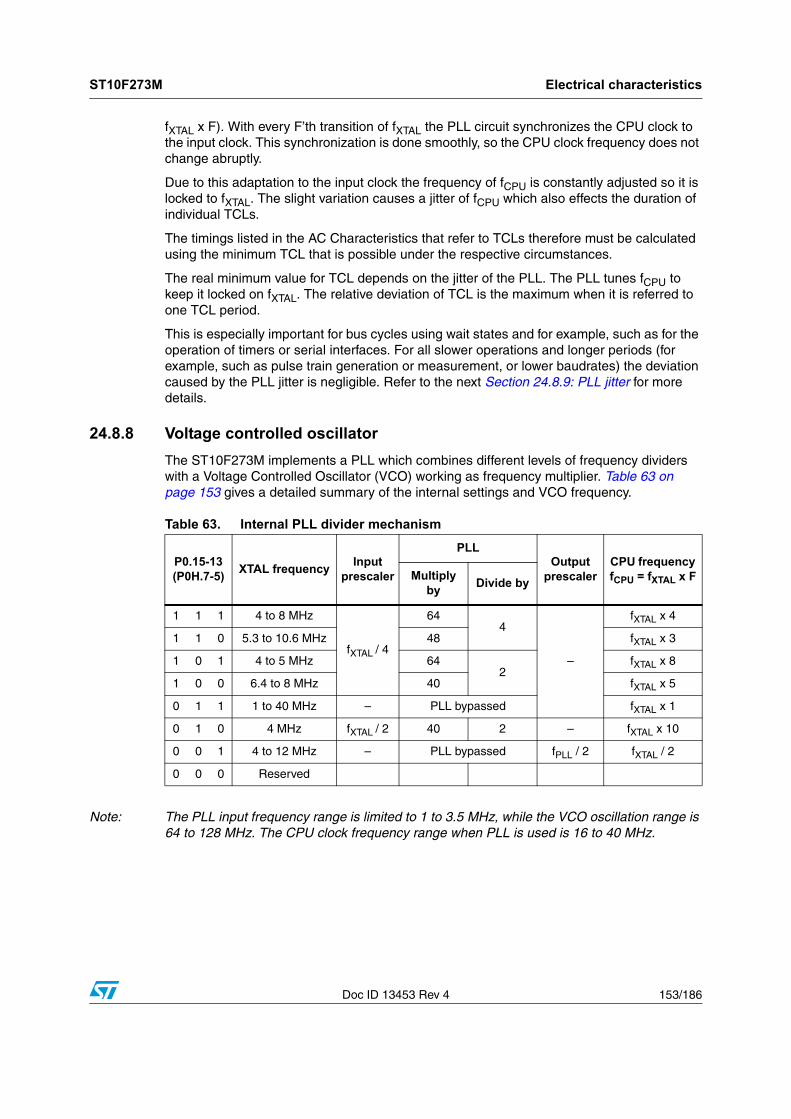
ST10F273M Electrical characteristics
Doc ID 13453 Rev 4 153/186
fXTAL x F). With every F’th transition of fXTAL the PLL circuit synchronizes the CPU clock to the input clock. This synchronization is done smoothly, so the CPU clock frequency does not change abruptly.
Due to this adaptation to the input clock the frequency of fCPU is constantly adjusted so it is locked to fXTAL. The slight variation causes a jitter of fCPU which also effects the duration of individual TCLs.
The timings listed in the AC Characteristics that refer to TCLs therefore must be calculated using the minimum TCL that is possible under the respective circumstances.
The real minimum value for TCL depends on the jitter of the PLL. The PLL tunes fCPU to keep it locked on fXTAL. The relative deviation of TCL is the maximum when it is referred to one TCL period.
This is especially important for bus cycles using wait states and for example, such as for the operation of timers or serial interfaces. For all slower operations and longer periods (for example, such as pulse train generation or measurement, or lower baudrates) the deviation caused by the PLL jitter is negligible. Refer to the next Section 24.8.9: PLL jitter for more details.
24.8.8 Voltage controlled oscillator
The ST10F273M implements a PLL which combines different levels of frequency dividers with a Voltage Controlled Oscillator (VCO) working as frequency multiplier. Table 63 on page 153 gives a detailed summary of the internal settings and VCO frequency.
Note: The PLL input frequency range is limited to 1 to 3.5 MHz, while the VCO oscillation range is 64 to 128 MHz. The CPU clock frequency range when PLL is used is 16 to 40 MHz.
Table 63. Internal PLL divider mechanism
P0.15-13(P0H.7-5)
XTAL frequencyInput
prescaler
PLLOutput
prescalerCPU frequency fCPU = fXTAL x FMultiply
byDivide by
1 1 1 4 to 8 MHz
fXTAL / 4
644
–
fXTAL x 4
1 1 0 5.3 to 10.6 MHz 48 fXTAL x 3
1 0 1 4 to 5 MHz 642
fXTAL x 8
1 0 0 6.4 to 8 MHz 40 fXTAL x 5
0 1 1 1 to 40 MHz – PLL bypassed fXTAL x 1
0 1 0 4 MHz fXTAL / 2 40 2 – fXTAL x 10
0 0 1 4 to 12 MHz – PLL bypassed fPLL / 2 fXTAL / 2
0 0 0 Reserved
Electrical characteristics ST10F273M
154/186 Doc ID 13453 Rev 4
Example 1
● fXTAL = 4 MHz
● P0(15:13) = ‘110’ (multiplication by 3)
● PLL Input Frequency = 1 MHz
● VCO frequency = 48 MHz: NOT VALID, must be 64 to 128 MHz
● fCPU = NOT VALID
Example 2
● fXTAL = 8 MHz
● P0(15:13) = ‘100’ (multiplication by 5)
● PLL Input Frequency = 2 MHz
● VCO frequency = 80 MHz
● PLL Output Frequency = 40 MHz (VCO frequency divided by 2)
● fCPU = 40 MHz (no effect of Output Prescaler)
24.8.9 PLL jitter
The following terminology is hereafter defined:
● Self referred single period jitterAlso called “Period Jitter”, it can be defined as the difference of the Tmax and Tmin, where Tmax is maximum time period of the PLL output clock and Tmin is the minimum time period of the PLL output clock.
● Self referred long term jitter Also called “N period jitter”, it can be defined as the difference of Tmax and Tmin, where Tmax is the maximum time difference between N + 1 clock rising edges and Tmin is the minimum time difference between N + 1 clock rising edges. Here N should be kept sufficiently large to have the long term jitter. For N = 1, this becomes the single period jitter.
Jitter at the PLL output can be due to the following reasons:
● Jitter in the input clock
● Noise in the PLL loop
Jitter in the input clock
PLL acts like a low pass filter for any jitter in the input clock. Input Clock jitter with the frequencies within the PLL loop bandwidth is passed to the PLL output and higher frequency jitter (frequency > PLL bandwidth) is attenuated @20dB/decade.
Noise in the PLL loop
This contribution again can be caused by the following sources:
● Device noise of the circuit in the PLL
● Noise in supply and substrate.
Device noise of the circuit in the PLL
The long term jitter is inversely proportional to the bandwidth of the PLL: the wider is the loop bandwidth, the lower is the jitter due to noise in the loop. Besides, the long term jitter is practically independent on the multiplication factor.
ST10F273M Electrical characteristics
Doc ID 13453 Rev 4 155/186
The most noise sensitive circuit in the PLL circuit is definitively the VCO (Voltage Controlled Oscillator). There are two main sources of noise: thermal (random noise, frequency independent so practically white noise) and flicker (low frequency noise, 1/f). For the frequency characteristics of the VCO circuitry, the effect of the thermal noise results in a 1/f2 region in the output noise spectrum, while the flicker noise in a 1/f3. Assuming a noiseless PLL input and supposing that the VCO is dominated by its 1/f2 noise, the R.M.S. value of the accumulated jitter is proportional to the square root of N, where N is the number of clock periods within the considered time interval.On the contrary, assuming again a noiseless PLL input and supposing that the VCO is dominated by its 1/f3 noise, the R.M.S. value of the accumulated jitter is proportional to N, where N is the number of clock periods within the considered time interval.
The jitter in the PLL loop can be modelized as dominated by the i1/f2 noise for N smaller than a certain value depending on the PLL output frequency and on the bandwidth characteristics of loop. Above this first value, the jitter becomes dominated by the i1/f3 noise component. Lastly, for N greater than a second value of N, a saturation effect is evident, so the jitter does not grow anymore when considering a longer time interval (jitter stable increasing the number of clock periods N). The PLL loop acts as a high pass filter for any noise in the loop, with cutoff frequency equal to the bandwidth of the PLL. The saturation value corresponds to what has been called self referred long term jitter of the PLL. In Figure 47 the maximum jitter trend versus the number of clock periods N (for some typical CPU frequencies) is reported: the curves represent the very worst case, computed taking into account all corners of temperature, power supply and process variations: the real jitter is always measured well below the given worst case values.
Noise in supply and substrate
Digital supply noise adds deterministic components to the PLL output jitter, independent on multiplication factor. Its effects is strongly reduced thanks to particular care used in the physical implementation and integration of the PLL module inside the device. Anyhow, the contribution of the digital noise to the global jitter is widely taken into account in the curves provided in Figure 47.

Electrical characteristics ST10F273M
156/186 Doc ID 13453 Rev 4
Figure 47. ST10F273M PLL jitter
24.8.10 PLL lock / unlock
During normal operation, if the PLL gets unlocked for any reason, an interrupt request to the CPU is generated, and the reference clock (oscillator) is automatically disconnected from the PLL input: in this way, the PLL goes into free-running mode, providing the system with a backup clock signal (free running frequency ffree). This feature allows to recover from a crystal failure occurrence without risking to go into an undefined configuration: The system is provided with a clock allowing the execution of the PLL unlock interrupt routine in a safe mode.
The path between reference clock and PLL input can be restored only by a hardware reset, or by a bidirectional software or watchdog reset event that forces the RSTIN pin low.
Note: The external RC circuit on RSTIN pin shall be properly sized in order to extend the duration of the low pulse to grant the PLL gets locked before the level at RSTIN pin is recognized high: bidirectional reset internally drives RSTIN pin low for just 1024 TCL (definitively not sufficient to get the PLL locked starting from free-running mode).
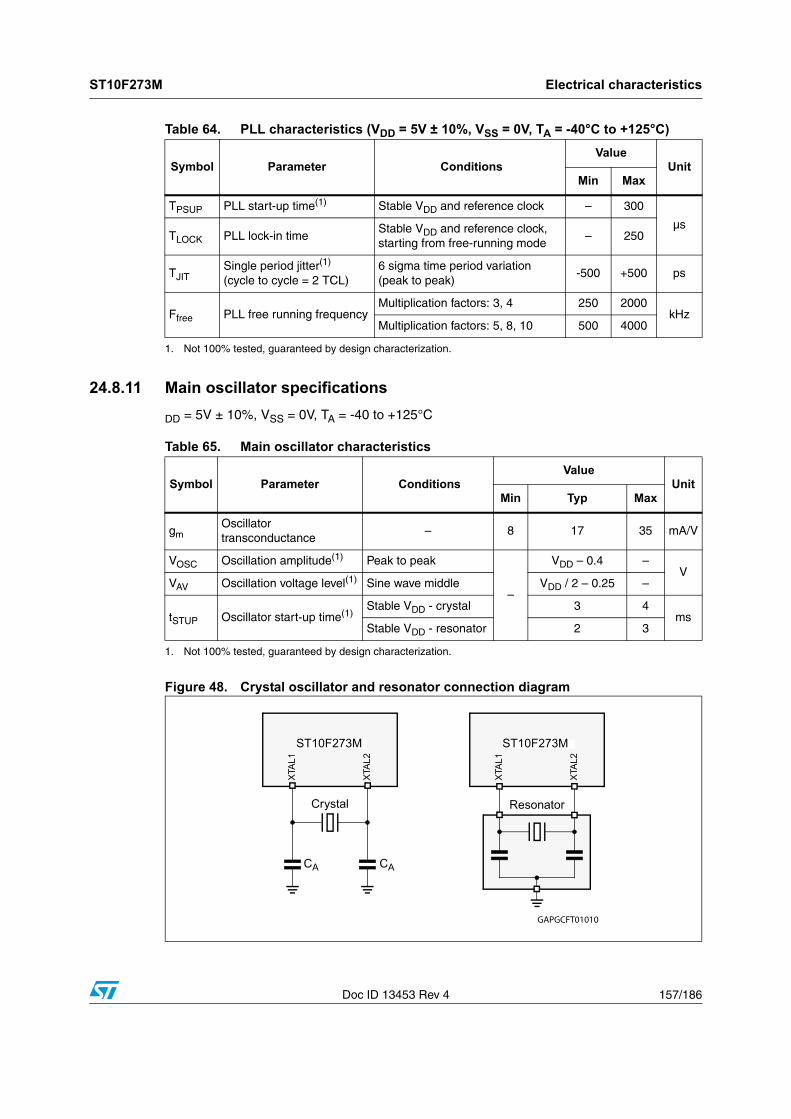
ST10F273M Electrical characteristics
Doc ID 13453 Rev 4 157/186
24.8.11 Main oscillator specifications
DD = 5V ± 10%, VSS = 0V, TA = -40 to +125°C
Figure 48. Crystal oscillator and resonator connection diagram
Table 64. PLL characteristics (VDD = 5V ± 10%, VSS = 0V, TA = -40°C to +125°C)
Symbol Parameter ConditionsValue
UnitMin Max
TPSUP PLL start-up time(1)
1. Not 100% tested, guaranteed by design characterization.
Stable VDD and reference clock – 300
µsTLOCK PLL lock-in time
Stable VDD and reference clock, starting from free-running mode
– 250
TJITSingle period jitter(1)
(cycle to cycle = 2 TCL) 6 sigma time period variation(peak to peak)
-500 +500 ps
Ffree PLL free running frequencyMultiplication factors: 3, 4 250 2000
kHzMultiplication factors: 5, 8, 10 500 4000
Table 65. Main oscillator characteristics
Symbol Parameter ConditionsValue
UnitMin Typ Max
gmOscillatortransconductance
– 8 17 35 mA/V
VOSC Oscillation amplitude(1)
1. Not 100% tested, guaranteed by design characterization.
Peak to peak
–
VDD – 0.4 –V
VAV Oscillation voltage level(1) Sine wave middle VDD / 2 – 0.25 –
tSTUP Oscillator start-up time(1)Stable VDD - crystal 3 4
msStable VDD - resonator 2 3

Electrical characteristics ST10F273M
158/186 Doc ID 13453 Rev 4
The given values of CA do not include the stray capacitance of the package and of the printed circuit board: the negative resistance values are calculated assuming additional 5pF to the values in the table. The crystal shunt capacitance (C0), the package and the stray capacitance between XTAL1 and XTAL2 pins is globally assumed equal to 4pF.
The external resistance between XTAL1 and XTAL2 is not necessary, since already present on the silicon.
24.8.12 32 kHz oscillator specifications
VDD = 5V ± 10%, VSS = 0V, TA = -40 to +125°C
Figure 49. 32 kHz crystal oscillator connection diagram
Table 66. Main oscillator negative resistance (module)
CA = 12pF 15pF 18pF 22pF 27pF 33pF 39pF 47pF
4 MHz 460 Ω 550 Ω 675 Ω 800 Ω 840 Ω 1000 Ω 1180 Ω 1200 Ω
8 MHz 380 Ω 460 Ω 540 Ω 640 Ω 580 Ω - - -
12 MHz 370 Ω 420 Ω 360 Ω - - - - -
Table 67. 32 kHz oscillator characteristics
Symbol Parameter ConditionsValue
UnitMin Typ Max
gm32 Oscillator transconductance(1)
1. At power-on a high current biasing is applied for faster oscillation start-up. Once the oscillation is started, the current biasing is reduced to lower the power consumption of the system.
Start-up 20 31 50µA/V
Normal run 8 17 30
VOSC32 Oscillation amplitude(2)
2. Not 100% tested, guaranteed by design characterization.
Peak to peak 0.5 1.0 2.4V
VAV32 Oscillation voltage level(2) Sine wave middle 0.7 0.9 1.2
tSTUP32 Oscillator start-up time(2) Stable VDD – 1 5 s
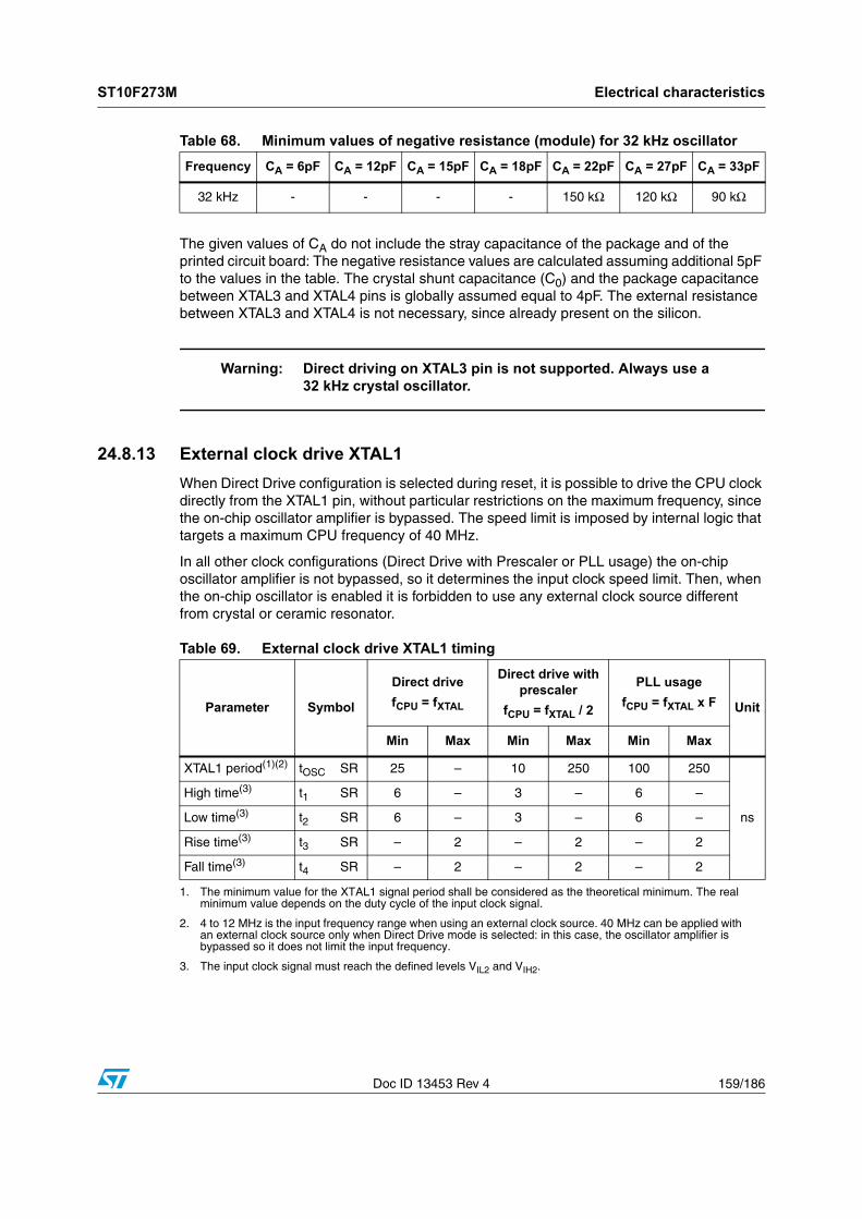
ST10F273M Electrical characteristics
Doc ID 13453 Rev 4 159/186
The given values of CA do not include the stray capacitance of the package and of the printed circuit board: The negative resistance values are calculated assuming additional 5pF to the values in the table. The crystal shunt capacitance (C0) and the package capacitance between XTAL3 and XTAL4 pins is globally assumed equal to 4pF. The external resistance between XTAL3 and XTAL4 is not necessary, since already present on the silicon.
Warning: Direct driving on XTAL3 pin is not supported. Always use a 32 kHz crystal oscillator.
24.8.13 External clock drive XTAL1
When Direct Drive configuration is selected during reset, it is possible to drive the CPU clock directly from the XTAL1 pin, without particular restrictions on the maximum frequency, since the on-chip oscillator amplifier is bypassed. The speed limit is imposed by internal logic that targets a maximum CPU frequency of 40 MHz.
In all other clock configurations (Direct Drive with Prescaler or PLL usage) the on-chip oscillator amplifier is not bypassed, so it determines the input clock speed limit. Then, when the on-chip oscillator is enabled it is forbidden to use any external clock source different from crystal or ceramic resonator.
Table 68. Minimum values of negative resistance (module) for 32 kHz oscillator
Frequency CA = 6pF CA = 12pF CA = 15pF CA = 18pF CA = 22pF CA = 27pF CA = 33pF
32 kHz - - - - 150 kΩ 120 kΩ 90 kΩ
Table 69. External clock drive XTAL1 timing
Parameter Symbol
Direct drive
fCPU = fXTAL
Direct drive with prescaler
fCPU = fXTAL / 2
PLL usage
fCPU = fXTAL x F Unit
Min Max Min Max Min Max
XTAL1 period(1)(2)
1. The minimum value for the XTAL1 signal period shall be considered as the theoretical minimum. The real minimum value depends on the duty cycle of the input clock signal.
2. 4 to 12 MHz is the input frequency range when using an external clock source. 40 MHz can be applied with an external clock source only when Direct Drive mode is selected: in this case, the oscillator amplifier is bypassed so it does not limit the input frequency.
tOSC SR 25 – 10 250 100 250
ns
High time(3)
3. The input clock signal must reach the defined levels VIL2 and VIH2.
t1 SR 6 – 3 – 6 –
Low time(3) t2 SR 6 – 3 – 6 –
Rise time(3) t3 SR – 2 – 2 – 2
Fall time(3) t4 SR – 2 – 2 – 2

Electrical characteristics ST10F273M
160/186 Doc ID 13453 Rev 4
Figure 50. External clock drive XTAL1
Note: When Direct Drive is selected, an external clock source can be used to drive XTAL1. The maximum frequency of the external clock source depends on the duty cycle: when 40 MHz is used, 50% duty cycle shall be granted (low phase = high phase = 12.5ns); when for instance 20 MHz is used, a 25% duty cycle can be accepted (minimum phase, high or low, again equal to 12.5ns).
24.8.14 Memory cycle variables
The tables below use three variables which are derived from the BUSCONx registers and represent the special characteristics of the programmed memory cycle. The following table describes how these variables are to be computed.
24.8.15 External memory bus timing
The following sections present the External Memory Bus timings. The given values are computed for a maximum CPU clock of 40 MHz.
Note: All external memory bus timings and SSC timings reported in the following tables are based on design characterization and not fully tested in production.
24.8.16 Multiplexed bus
VDD = 5V ± 10%, VSS = 0V, TA = -40 to +125°C, CL = 50pF, ALE cycle time = 6 TCL + 2tA + tC + tF (75ns at 40 MHz CPU clock without wait states)
Table 70. Memory cycle variables
Description Symbol Values
ALE Extension tA TCL x [ALECTL]
Memory Cycle Time wait states tC 2TCL x (15 - [MCTC])
Memory Tri-stateTime tF 2TCL x (1 - [MTTC])
Table 71. Multiplexed bus timings
Symbol Parameter
fCPU = 40 MHzTCL = 12.5ns
Variable CPU clock1/2 TCL = 1 to 40 MHz Unit
Min Max Min Max
t5 CC ALE high time 4 + tA – TCL - 8.5 + tA – ns
t6 CC Address setup to ALE 1.5 + tA – TCL - 11 + tA – ns

ST10F273M Electrical characteristics
Doc ID 13453 Rev 4 161/186
t7 CC Address hold after ALE 4 + tA – TCL - 8.5 + tA – ns
t8 CCALE falling edge to RD, WR (with RW-delay)
4 + tA – TCL - 8.5 + tA – ns
t9 CCALE falling edge to RD, WR (no RW-delay)
-8.5 + tA – -8.5 + tA – ns
t10 CCAddress float after RD, WR (with RW-delay)
– 6 – 6 ns
t11 CCAddress float after RD, WR (no RW-delay)1
– 18.5 – TCL + 6 ns
t12 CCRD, WR low time(with RW-delay)
15.5 + tC – 2TCL - 9.5 + tC – ns
t13 CCRD, WR low time(no RW-delay)
28 + tC – 3TCL - 9.5 + tC – ns
t14 SRRD to valid data in(with RW-delay)
– 6 + tC – 2TCL - 19 + tC ns
t15 SRRD to valid data in (no RW-delay)
– 18.5 + tC – 3TCL - 19 + tC ns
t16 SR ALE low to valid data in – 17.5 + tA + tC – 3TCL - 20 + tA + tC ns
t17 SRAddress/Unlatched CS to valid data in
– 20 + 2tA + tC – 4TCL - 30 + 2tA + tC ns
t18 SRData hold after RDrising edge
0 – 0 – ns
t19 SR Data float after RD1 – 16.5 + tF – 2TCL - 8.5 + tF ns
t22 CC Data valid to WR 10 + tC – 2TCL - 15 + tC – ns
t23 CC Data hold after WR 4 + tF – 2TCL - 8.5 + tF – ns
t25 CC ALE rising edge after RD, WR 15 + tF – 2TCL - 10 + tF – ns
t27 CCAddress/unlatched CS hold after RD, WR
10 + tF – 2TCL - 15 + tF – ns
t38 CC ALE falling edge to latched CS -4 - tA 10 - tA -4 - tA 10 - tA ns
t39 SR Latched CS low to valid data in – 16.5 + tC + 2tA – 3TCL - 21 + tC + 2tA ns
t40 CC Latched CS hold after RD, WR 27 + tF – 3TCL - 10.5 + tF – ns
t42 CCALE fall. edge to RdCS, WrCS (with RW delay)
7 + tA – TCL - 5.5 + tA – ns
t43 CCALE fall. edge to RdCS, WrCS (no RW delay)
-5.5 + tA – -5.5 + tA – ns
t44 CCAddress float after RdCS, WrCS(with RW delay)
– 1.5 – 1.5 ns
Table 71. Multiplexed bus timings (continued)
Symbol Parameter
fCPU = 40 MHzTCL = 12.5ns
Variable CPU clock1/2 TCL = 1 to 40 MHz Unit
Min Max Min Max

Electrical characteristics ST10F273M
162/186 Doc ID 13453 Rev 4
t45 CCAddress float after RdCS, WrCS(no RW delay)
– 14 – TCL + 1.5 ns
t46 SRRdCS to Valid Data in(with RW delay)
– 4 + tC – 2TCL - 21 + tC ns
t47 SRRdCS to Valid Data in(no RW delay)
– 16.5 + tC – 3TCL - 21 + tC ns
t48 CCRdCS, WrCS Low Time(with RW delay)
15.5 + tC – 2TCL - 9.5 + tC – ns
t49 CCRdCS, WrCS Low Time(no RW delay)
28 + tC – 3TCL - 9.5 + tC – ns
t50 CC Data valid to WrCS 10 + tC – 2TCL - 15 + tC – ns
t51 SR Data hold after RdCS 0 – 0 – ns
t52 SR Data float after RdCS1 – 16.5 + tF – 2TCL - 8.5 + tF ns
t54 CCAddress hold afterRdCS, WrCS
6 + tF – 2TCL - 19 + tF – ns
t56 CC Data hold after WrCS 6 + tF – 2TCL - 19 + tF – ns
Table 71. Multiplexed bus timings (continued)
Symbol Parameter
fCPU = 40 MHzTCL = 12.5ns
Variable CPU clock1/2 TCL = 1 to 40 MHz Unit
Min Max Min Max

ST10F273M Electrical characteristics
Doc ID 13453 Rev 4 163/186
Figure 51. External memory cycle: multiplexed bus, with/ without read/ write delay, normal ALE

Electrical characteristics ST10F273M
164/186 Doc ID 13453 Rev 4
Figure 52. External memory cycle: multiplexed bus, with/ without read/ write delay, extended ALE
Data OutAddress
Data InAddress
Address
t5 t16
t6 t7
t39
t40
t14
t8
t18
t23
t6
t27
t38
t10 t19
t25
t17
t9 t11
t15
t12
t13
t8 t10
t9 t11
t12t13
t22
t27
t17
t6
Read Cycle
Write Cycle
CLKOUT
ALE
CSx
A23-A16(A15-A8)
RD
WRWRL
BHE
WRH
Address/DataBus (P0)
Address/DataBus (P0)
GAPGCFT00935

ST10F273M Electrical characteristics
Doc ID 13453 Rev 4 165/186
Figure 53. External memory cycle: multiplexed bus, with/ without read/ write delay, normal ALE, read/ write chip select
Read Cycle
Write Cycle
CLKOUT
ALE
A23-A16(A15-A8)BHE
Data In
Data OutAddress
Address
t44
t5 t16 t25
t27
t51
t46
t50
t56
t48
t42
t42
t6
t52
Address
t17
t6
t7
t43 t45
t49
t47
t16
t48t49
Address
t43
RdCSx
WrCSx
Address/DataBus (P0)
Address/DataBus (P0)
GAPGCFT00936

Electrical characteristics ST10F273M
166/186 Doc ID 13453 Rev 4
Figure 54. External memory cycle: multiplexed bus, with/ without read/ write delay, extended ALE, read/ write chip select
Data OutAddress
Data InAddress
Address
t5 t16
t6 t7
t46
t42
t42
t50
t18
t56
t6
t54
t44
t19
t25
t17
t43 t45
t47
t48
t49
t49
t43
t48
t44
t45
Read Cycle
Write Cycle
CLKOUT
ALE
A23-A16(A15-A8)BHE
RdCSx
WrCSx
Address/DataBus (P0)
Address/DataBus (P0)
GAPGCFT00937
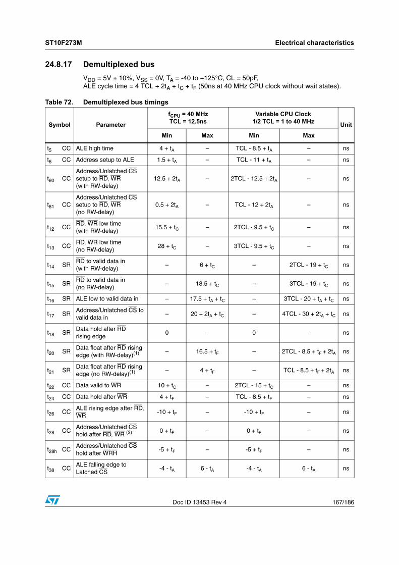
ST10F273M Electrical characteristics
Doc ID 13453 Rev 4 167/186
24.8.17 Demultiplexed bus
VDD = 5V ± 10%, VSS = 0V, TA = -40 to +125°C, CL = 50pF, ALE cycle time = 4 TCL + 2tA + tC + tF (50ns at 40 MHz CPU clock without wait states).
Table 72. Demultiplexed bus timings
Symbol Parameter
fCPU = 40 MHzTCL = 12.5ns
Variable CPU Clock1/2 TCL = 1 to 40 MHz Unit
Min Max Min Max
t5 CC ALE high time 4 + tA – TCL - 8.5 + tA – ns
t6 CC Address setup to ALE 1.5 + tA – TCL - 11 + tA – ns
t80 CCAddress/Unlatched CS setup to RD, WR (with RW-delay)
12.5 + 2tA – 2TCL - 12.5 + 2tA – ns
t81 CCAddress/Unlatched CS setup to RD, WR (no RW-delay)
0.5 + 2tA – TCL - 12 + 2tA – ns
t12 CCRD, WR low time(with RW-delay)
15.5 + tC – 2TCL - 9.5 + tC – ns
t13 CCRD, WR low time(no RW-delay)
28 + tC – 3TCL - 9.5 + tC – ns
t14 SRRD to valid data in(with RW-delay)
– 6 + tC – 2TCL - 19 + tC ns
t15 SRRD to valid data in(no RW-delay)
– 18.5 + tC – 3TCL - 19 + tC ns
t16 SR ALE low to valid data in – 17.5 + tA + tC – 3TCL - 20 + tA + tC ns
t17 SRAddress/Unlatched CS to valid data in
– 20 + 2tA + tC – 4TCL - 30 + 2tA + tC ns
t18 SRData hold after RDrising edge
0 – 0 – ns
t20 SRData float after RD rising edge (with RW-delay)(1) – 16.5 + tF – 2TCL - 8.5 + tF + 2tA ns
t21 SRData float after RD rising edge (no RW-delay)(1) – 4 + tF – TCL - 8.5 + tF + 2tA ns
t22 CC Data valid to WR 10 + tC – 2TCL - 15 + tC – ns
t24 CC Data hold after WR 4 + tF – TCL - 8.5 + tF – ns
t26 CCALE rising edge after RD, WR
-10 + tF – -10 + tF – ns
t28 CCAddress/Unlatched CS hold after RD, WR (2) 0 + tF – 0 + tF – ns
t28h CCAddress/Unlatched CS hold after WRH
-5 + tF – -5 + tF – ns
t38 CCALE falling edge to Latched CS
-4 - tA 6 - tA -4 - tA 6 - tA ns

Electrical characteristics ST10F273M
168/186 Doc ID 13453 Rev 4
t39 SRLatched CS low to Valid Data in
– 16.5 + tC + 2tA – 3TCL - 21 + tC + 2tA ns
t41 CCLatched CS hold after RD, WR
2 + tF – TCL - 10.5 + tF – ns
t82 CCAddress setup to RdCS, WrCS(with RW-delay)
14 + 2tA – 2TCL - 11 + 2tA – ns
t83 CCAddress setup to RdCS, WrCS(no RW-delay)
2 + 2tA – TCL - 10.5 + 2tA – ns
t46 SRRdCS to Valid Data in(with RW-delay)
– 4 + tC – 2TCL - 21 + tC ns
t47 SRRdCS to Valid Data in(no RW-delay)
– 16.5 + tC – 3TCL - 21 + tC ns
t48 CCRdCS, WrCS Low Time(with RW-delay)
15.5 + tC – 2TCL - 9.5 + tC – ns
t49 CCRdCS, WrCS Low Time(no RW-delay)
28 + tC – 3TCL - 9.5 + tC – ns
t50 CC Data valid to WrCS 10 + tC – 2TCL - 15 + tC – ns
t51 SR Data hold after RdCS 0 – 0 – ns
t53 SRData float after RdCS(with RW-delay) 3
– 16.5 + tF – 2TCL - 8.5 + tF ns
t68 SRData float after RdCS(no RW-delay) 3
– 4 + tF – TCL - 8.5 + tF ns
t55 CCAddress hold afterRdCS, WrCS
-8.5 + tF – -8.5 + tF – ns
t57 CC Data hold after WrCS 2 + tF – TCL - 10.5 + tF – ns
1. RW-delay and tA refer to the next following bus cycle
2. Read data are latched with the same clock edge that triggers the address change and the rising RD edge. Therefore address changes before the end of RD have no impact on read cycles.
Table 72. Demultiplexed bus timings (continued)
Symbol Parameter
fCPU = 40 MHzTCL = 12.5ns
Variable CPU Clock1/2 TCL = 1 to 40 MHz Unit
Min Max Min Max
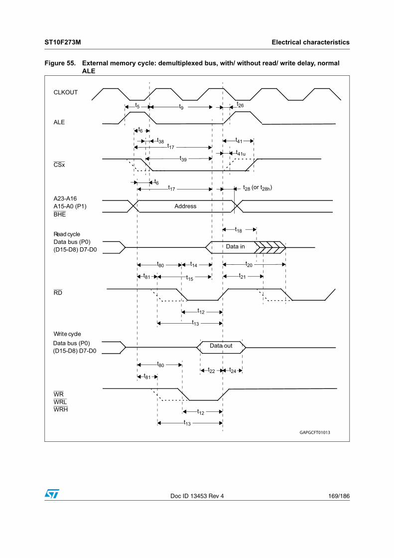
ST10F273M Electrical characteristics
Doc ID 13453 Rev 4 169/186
Figure 55. External memory cycle: demultiplexed bus, with/ without read/ write delay, normal ALE
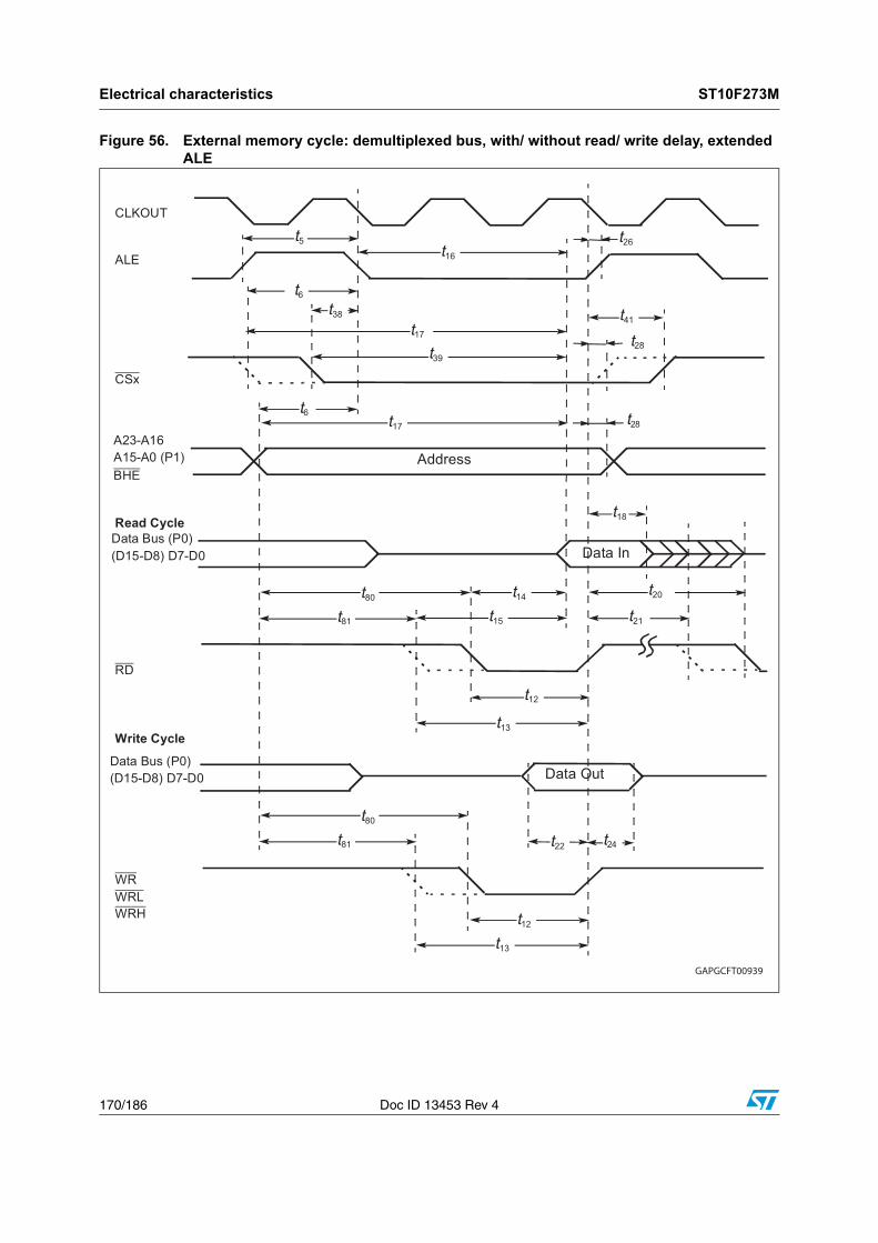
Electrical characteristics ST10F273M
170/186 Doc ID 13453 Rev 4
Figure 56. External memory cycle: demultiplexed bus, with/ without read/ write delay, extended ALE
Address
t5t16
t39
t41
t14
t24
t6
t38
t20
t26
t17
t15
t12
t13
t12
t13
t22
Data In
t18
t21
t6
t17 t28
t28
Data Out
t80
t81
t80
t81
Read Cycle
Write Cycle
CLKOUT
ALE
CSx
RD
WRWRLWRH
Data Bus (P0)(D15-D8) D7-D0
Data Bus (P0)(D15-D8) D7-D0
A23-A16A15-A0 (P1)BHE
GAPGCFT00939

ST10F273M Electrical characteristics
Doc ID 13453 Rev 4 171/186
Figure 57. External memory cycle: demultiplexed bus, with/ without read/ write delay, normal ALE, read/ write chip select
Read Cycle
Write Cycle
CLKOUT
ALE
Data In
Data Out
t5 t16
t51
t46
t50
t48
Address
t17
t49
t47
t48
t49
t68
t53
t83
t82
t26
t57
t55
t6
t82
t83
RdCSx
WrCSx
Data Bus (P0)(D15-D8) D7-D0
Data Bus (P0)(D15-D8) D7-D0
A23-A16A15-A0 (P1)BHE
GAPGCFT00940
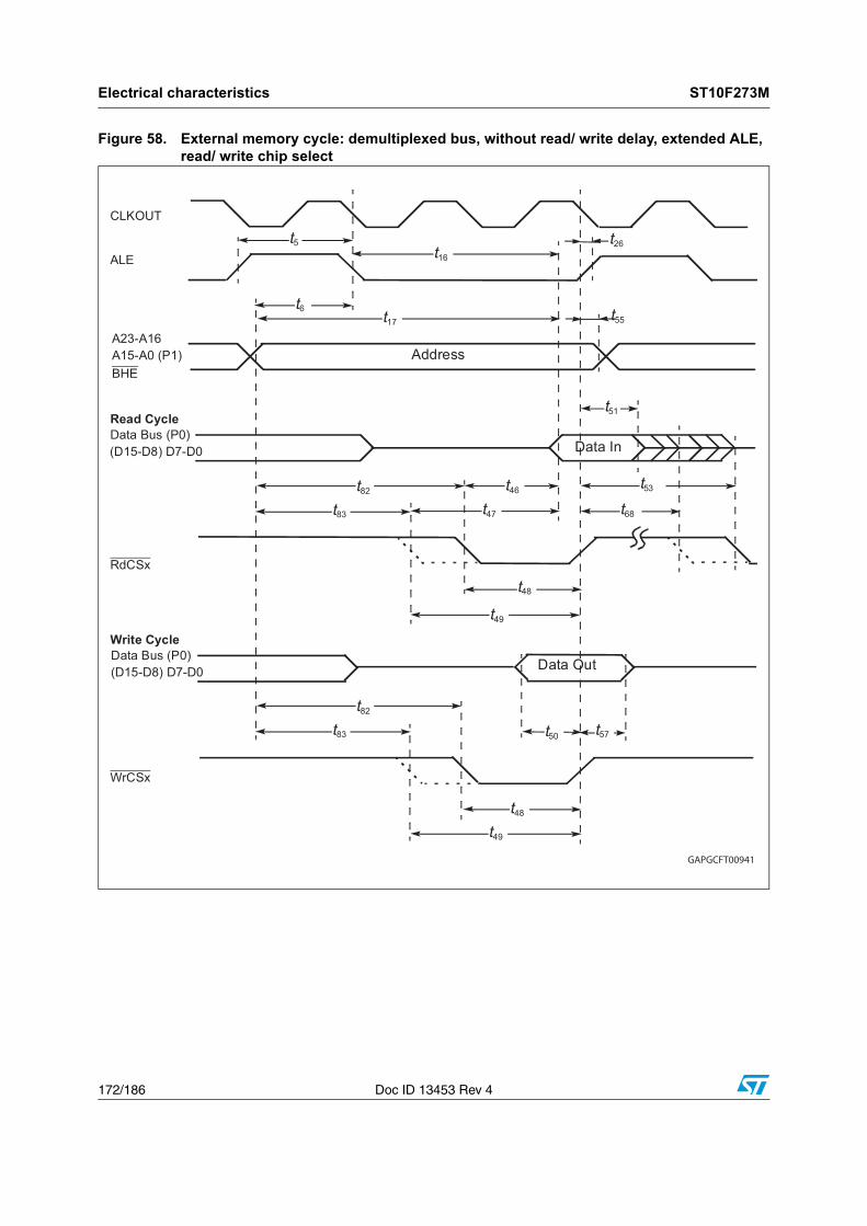
Electrical characteristics ST10F273M
172/186 Doc ID 13453 Rev 4
Figure 58. External memory cycle: demultiplexed bus, without read/ write delay, extended ALE, read/ write chip select
Address
t5t16
t46
t57
t6
t53
t26
t17
t47
t48
t49
t48
t49
t50
Data In
t51
t68
t55
Data Out
t82
t83
t82
t83
Read Cycle
Write Cycle
CLKOUT
ALE
RdCSx
WrCSx
Data Bus (P0)(D15-D8) D7-D0
Data Bus (P0)(D15-D8) D7-D0
A23-A16A15-A0 (P1)BHE
GAPGCFT00941

ST10F273M Electrical characteristics
Doc ID 13453 Rev 4 173/186
24.8.18 CLKOUT and READY
VDD = 5V ± 10%, VSS = 0V, TA = -40 to + 125°C, CL = 50pF
Table 73. CLKOUT and READY timings
Symbol Parameter
fCPU = 40 MHzTCL = 12.5ns
Variable CPU clock1/2 TCL = 1 to 40 MHz Unit
Min Max Min Max
t29 CC CLKOUT cycle time 25 25 2TCL 2TCL
ns
t30 CC CLKOUT high time 9 – TCL – 3.5 –
t31 CC CLKOUT low time 10 – TCL – 2.5 –
t32 CC CLKOUT rise time – 4 – 4
t33 CC CLKOUT fall time – 4 – 4
t34 CCCLKOUT rising edge to ALE falling edge
– 2 + tA 8 + tA – 2 + tA 8 + tA
t35 SRSynchronous READYsetup time to CLKOUT
17 – 17 –
t36 SRSynchronous READYhold time after CLKOUT
2 – 2 –
t37 SRAsynchronous READYlow time
35 – 2TCL + 10 –
t58 SRAsynchronous READYsetup time(1)
1. These timings are given for characterization purposes only, in order to assure recognition at a specific clock edge.
17 – 17 –
t59 SRAsynchronous READYhold time (1) 2 – 2 –
t60 SRAsync. READY hold time after RD, WR high (Demultiplexed bus)(2)
2. Demultiplexed bus is the worst case. For multiplexed bus 2TCL are to be added to the maximum values. This adds even more time for deactivating READY. 2tA and tC refer to the next following bus cycle, tF refers to the current bus cycle.
0 2tA + tC + tF 0 2tA + tC + tF

Electrical characteristics ST10F273M
174/186 Doc ID 13453 Rev 4
Figure 59. CLKOUT and READY
1. Cycle as programmed, including MCTC wait states (Example shows 0 MCTC WS).
2. The leading edge of the respective command depends on RW-delay.
3. READY sampled HIGH at this sampling point generates a READY controlled wait state, READY sampled LOW at this sampling point terminates the currently running bus cycle.
4. READY may be deactivated in response to the trailing (rising) edge of the corresponding command (RD or WR).
5. If the Asynchronous READY signal does not fulfill the indicated setup and hold times with respect to CLKOUT (for example, because CLKOUT is not enabled), it must fulfill t37 in order to be safely synchronized. This is guaranteed, if READY is removed in response to the command (see Note 4).
6. Multiplexed bus modes have a MUX wait state added after a bus cycle, and an additional MTTC wait state may be inserted here.For a multiplexed bus with MTTC wait state this delay is two CLKOUT cycles, for a demultiplexed bus without MTTC wait state this delay is zero.
7. The next external bus cycle may start here.
24.8.19 External bus arbitration
VDD = 5V ± 10%, VSS = 0V, TA = -40 to +125°C, CL = 50pF
t30
t34
t35 t36 t35 t36
t58 t59 t58 t59
wait stateREADY
MUX / Tri-state 6)
t32 t33
t29
Running cycle 1)
t31
t37
3)3)
5)
t60 4)
6)
2)
7)
3) 3)
CLKOUT
ALE
RD, WR
Synchronous
Asynchronous
READY
READY
GAPGCFT00942
Table 74. External bus arbitration timings
Symbol Parameter
fCPU = 40 MHzTCL = 12.5ns
Variable CPU clock1/2 TCL = 1 to 40 MHz Unit
Min Max Min Max
t61 SR HOLD input setup time to CLKOUT 18.5 – 18.5 – ns
t62 CCCLKOUT to HLDA highor BREQ low delay
– 12.5 – 12.5 ns

ST10F273M Electrical characteristics
Doc ID 13453 Rev 4 175/186
Figure 60. External bus arbitration (releasing the bus)
1. The ST10F273M will complete the currently running bus cycle before granting bus access.
2. This is the first possibility for BREQ to become active.
3. The CS outputs will be resistive high (pull-up) after t64.
t63 CCCLKOUT to HLDA lowor BREQ high delay
– 12.5 – 12.5 ns
t64 CC CSx release(1) – 20 – 20 ns
t65 CC CSx drive -4 15 -4 15 ns
t66 CC Other signals release(1) – 20 – 20 ns
t67 CC Other signals drive -4 15 -4 15 ns
1. Partially tested, guaranteed by design characterization
Table 74. External bus arbitration timings (continued)
Symbol Parameter
fCPU = 40 MHzTCL = 12.5ns
Variable CPU clock1/2 TCL = 1 to 40 MHz Unit
Min Max Min Max
t61
t63
t66
1)
t64
1)
2)
t62
3)
CLKOUT
HOLD
HLDA
BREQ
Others
CSx(P6.x)
GAPGCFT00943
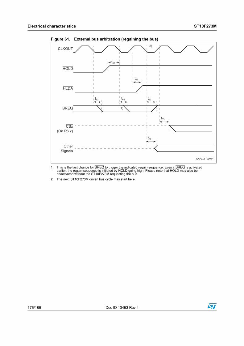
Electrical characteristics ST10F273M
176/186 Doc ID 13453 Rev 4
Figure 61. External bus arbitration (regaining the bus)
1. This is the last chance for BREQ to trigger the indicated regain-sequence. Even if BREQ is activated earlier, the regain-sequence is initiated by HOLD going high. Please note that HOLD may also be deactivated without the ST10F273M requesting the bus.
2. The next ST10F273M driven bus cycle may start here.
CLKOUT
HOLD
HLDA
OtherSignals
t62
CSx(On P6.x)
t67
t62
1)
2)
t65
t61
BREQ
t63t62
GAPGCFT00944
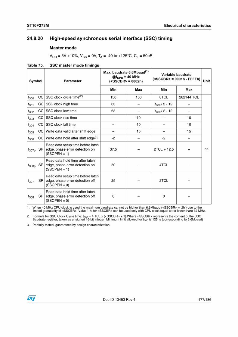
ST10F273M Electrical characteristics
Doc ID 13453 Rev 4 177/186
24.8.20 High-speed synchronous serial interface (SSC) timing
Master mode
VDD = 5V ±10%, VSS = 0V, TA = -40 to +125°C, CL = 50pF
Table 75. SSC master mode timings
Symbol Parameter
Max. baudrate 6.6Mbaud(1)
@fCPU = 40 MHz(<SSCBR> = 0002h)
Variable baudrate(<SSCBR> = 0001h - FFFFh) Unit
Min Max Min Max
t300 CC SSC clock cycle time(2) 150 150 8TCL 262144 TCL
ns
t301 CC SSC clock high time 63 – t300 / 2 - 12 –
t302 CC SSC clock low time 63 – t300 / 2 - 12 –
t303 CC SSC clock rise time – 10 – 10
t304 CC SSC clock fall time – 10 – 10
t305 CC Write data valid after shift edge – 15 – 15
t306 CC Write data hold after shift edge(3) -2 – -2 –
t307p SRRead data setup time before latch edge, phase error detection on (SSCPEN = 1)
37.5 – 2TCL + 12.5 –
t308p SRRead data hold time after latch edge, phase error detection on (SSCPEN = 1)
50 – 4TCL –
t307 SRRead data setup time before latch edge, phase error detection off (SSCPEN = 0)
25 – 2TCL –
t308 SRRead data hold time after latch edge, phase error detection off (SSCPEN = 0)
0 – 0 –
1. When 40 MHz CPU clock is used the maximum baudrate cannot be higher than 6.6Mbaud (<SSCBR> = ‘2h’) due to the limited granularity of <SSCBR>. Value ‘1h’ for <SSCBR> can be used only with CPU clock equal to (or lower than) 32 MHz.
2. Formula for SSC Clock Cycle time: t300 = 4 TCL x (<SSCBR> + 1) Where <SSCBR> represents the content of the SSC Baudrate register, taken as unsigned 16-bit integer. Minimum limit allowed for t300 is 125ns (corresponding to 6.6Mbaud)
3. Partially tested, guaranteed by design characterization
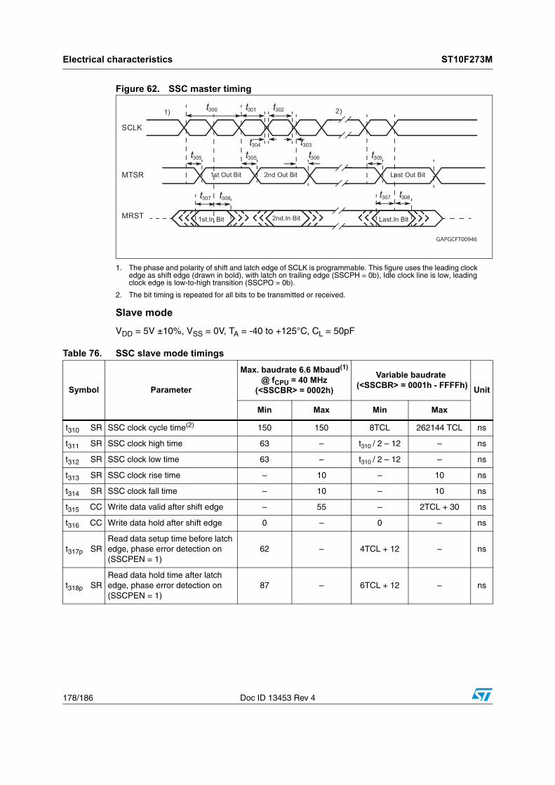
Electrical characteristics ST10F273M
178/186 Doc ID 13453 Rev 4
Figure 62. SSC master timing
1. The phase and polarity of shift and latch edge of SCLK is programmable. This figure uses the leading clock edge as shift edge (drawn in bold), with latch on trailing edge (SSCPH = 0b), Idle clock line is low, leading clock edge is low-to-high transition (SSCPO = 0b).
2. The bit timing is repeated for all bits to be transmitted or received.
Slave mode
VDD = 5V ±10%, VSS = 0V, TA = -40 to +125°C, CL = 50pF
t303t304
t305 t305 t305t306
tiB tuO tsaLtiB tuO ts1 2nd Out Bit
t300 t302t3011) 2)
t307
2nd.In Bit1st.In Bit
t308 t307
Last.In Bit
t308
SCLK
MTSR
MRST
GAPGCFT00946
Table 76. SSC slave mode timings
Symbol Parameter
Max. baudrate 6.6 Mbaud(1)
@ fCPU = 40 MHz(<SSCBR> = 0002h)
Variable baudrate (<SSCBR> = 0001h - FFFFh)
Unit
Min Max Min Max
t310 SR SSC clock cycle time(2) 150 150 8TCL 262144 TCL ns
t311 SR SSC clock high time 63 – t310 / 2 – 12 – ns
t312 SR SSC clock low time 63 – t310 / 2 – 12 – ns
t313 SR SSC clock rise time – 10 – 10 ns
t314 SR SSC clock fall time – 10 – 10 ns
t315 CC Write data valid after shift edge – 55 – 2TCL + 30 ns
t316 CC Write data hold after shift edge 0 – 0 – ns
t317p SRRead data setup time before latch edge, phase error detection on (SSCPEN = 1)
62 – 4TCL + 12 – ns
t318p SRRead data hold time after latch edge, phase error detection on (SSCPEN = 1)
87 – 6TCL + 12 – ns

ST10F273M Electrical characteristics
Doc ID 13453 Rev 4 179/186
Figure 63. SSC slave timing
1. The phase and polarity of shift and latch edge of SCLK is programmable. This figure uses the leading clock edge as shift edge (drawn in bold), with latch on trailing edge (SSCPH = 0b), Idle clock line is low, leading clock edge is low-to-high transition (SSCPO = 0b).
2. The bit timing is repeated for all bits to be transmitted or received.
t317 SRRead data setup time before latch edge, phase error detection off (SSCPEN = 0)
6 – 6 – ns
t318 SRRead data hold time after latch edge, phase error detection off (SSCPEN = 0)
31 – 2TCL + 6 – ns
1. When 40 MHz CPU clock is used the maximum baudrate cannot be higher than 6.6Mbaud (<SSCBR> = ‘2h’) due to the limited granularity of <SSCBR>. Value ‘1h’ for <SSCBR> may be used only with CPU clock lower than 32 MHz (after checking that resulting timings are suitable for the master).
2. Formula for SSC Clock Cycle time: t310 = 4 TCL * (<SSCBR> + 1) Where <SSCBR> represents the content of the SSC Baudrate register, taken as unsigned 16-bit integer.Minimum limit allowed for t310 is 150ns (corresponding to 6.6Mbaud).
Table 76. SSC slave mode timings (continued)
Symbol Parameter
Max. baudrate 6.6 Mbaud(1)
@ fCPU = 40 MHz(<SSCBR> = 0002h)
Variable baudrate (<SSCBR> = 0001h - FFFFh) Unit
Min Max Min Max
t313t314
t315 t315 t315t316
tiB tuO tsaLtiB tuO ts1 2nd Out Bit
t310 t312t3111) 2)
t317
2nd.In Bit1st.In Bit
t318 t317
Last.In Bit
t318
SCLK
MRST
MTSR
GAPGCFT00947

Package information ST10F273M
180/186 Doc ID 13453 Rev 4
25 Package information
25.1 ECOPACK®
In order to meet environmental requirements, ST offers these devices in different grades of ECOPACK® packages, depending on their level of environmental compliance. ECOPACK® specifications, grade definitions and product status are available at: www.st.com.
ECOPACK® is an ST trademark.
25.2 PQFP144 mechanical data
Table 77. PQFP144 mechanical data
Dimmm
Min. Typ. Max.
A 4.10
A1 0.25 0.50
A2 3.20 3.40 3.60
b 0.29 0.45
c 0.11 0.23
D 30.95 31.20 31.45
D1 27.80 28.00 28.20
D3 22.75
E 30.95 31.20 31.45
E1 27.80 28.00 28.20
E3 22.75
e 0.65
L 0.73 0.88 1.03
L1 0.25
L2 1.60
k 0° 7°
ddd 0.10

ST10F273M Package information
Doc ID 13453 Rev 4 181/186
Figure 64. PQFP144 package dimensions
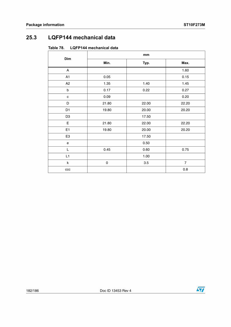
Package information ST10F273M
182/186 Doc ID 13453 Rev 4
25.3 LQFP144 mechanical data
Table 78. LQFP144 mechanical data
Dimmm
Min. Typ. Max.
A 1.60
A1 0.05 0.15
A2 1.35 1.40 1.45
b 0.17 0.22 0.27
c 0.09 0.20
D 21.80 22.00 22.20
D1 19.80 20.00 20.20
D3 17.50
E 21.80 22.00 22.20
E1 19.80 20.00 20.20
E3 17.50
e 0.50
L 0.45 0.60 0.75
L1 1.00
k 0 3.5 7
ccc 0.8

ST10F273M Package information
Doc ID 13453 Rev 4 183/186
Figure 65. LQFP144 package dimensions
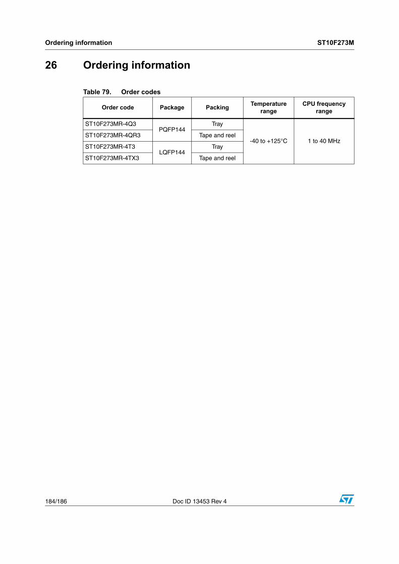
Ordering information ST10F273M
184/186 Doc ID 13453 Rev 4
26 Ordering information
Table 79. Order codes
Order code Package PackingTemperature
rangeCPU frequency
range
ST10F273MR-4Q3PQFP144
Tray
-40 to +125°C 1 to 40 MHzST10F273MR-4QR3 Tape and reel
ST10F273MR-4T3LQFP144
Tray
ST10F273MR-4TX3 Tape and reel
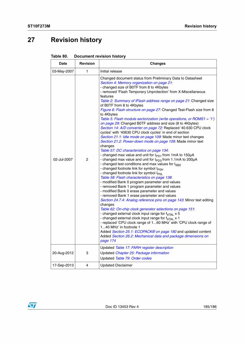
ST10F273M Revision history
Doc ID 13453 Rev 4 185/186
27 Revision history
Table 80. Document revision history
Date Revision Changes
03-May-2007 1 Initial release
02-Jul-2007 2
Changed document status from Preliminary Data to DatasheetSection 4: Memory organization on page 21:- changed size of B0TF from 8 to 4Kbytes- removed ‘Flash Temporary Unprotection’ from X-Miscellaneous featuresTable 2: Summary of IFlash address range on page 21: Changed size of B0TF from 8 to 4KbytesFigure 6: Flash structure on page 27: Changed Test-Flash size from 8 to 4KbytesTable 5: Flash module sectorization (write operations, or ROMS1 = ‘1’) on page 29: Changed B0TF address and size (8 to 4Kbytes)Section 14: A/D converter on page 72: Replaced ‘40.630 CPU clock cycles’ with ‘40630 CPU clock cycles’ in end of sectionSection 21.1: Idle mode on page 109: Made minor text changesSection 21.2: Power-down mode on page 109: Made minor text changesTable 57: DC characteristics on page 134:- changed max value and unit for IPD1 from 1mA to 150µA- changed max value and unit for IPD3 from 1.1mA to 200µA- changed test conditions and max values for ISB2- changed footnote link for symbol IP0H- changed footnote link for symbol IP0LTable 58: Flash characteristics on page 138:- modified Bank 0 program parameter and values- removed Bank 1 program parameter and values- modified Bank 0 erase parameter and values- removed Bank 1 erase parameter and valuesSection 24.7.4: Analog reference pins on page 143: Minor text editing changesTable 62: On-chip clock generator selections on page 151:- changed external clock input range for fXTAL x 5- changed external clock input range for fXTAL x 1- replaced ‘CPU clock range of 1...60 MHz’ with ‘CPU clock range of 1...40 MHz’ in footnote 1Added Section 25.1: ECOPACK® on page 180 and updated contentAdded Section 26.2: Mechanical data and package dimensions on page 174
20-Aug-2012 3
Updated Table 17: FARH register description
Updated Chapter 25: Package information
Updated Table 79: Order codes
17-Sep-2013 4 Updated Disclaimer

ST10F273M
186/186 Doc ID 13453 Rev 4
Please Read Carefully:
Information in this document is provided solely in connection with ST products. STMicroelectronics NV and its subsidiaries (“ST”) reserve theright to make changes, corrections, modifications or improvements, to this document, and the products and services described herein at anytime, without notice.
All ST products are sold pursuant to ST’s terms and conditions of sale.
Purchasers are solely responsible for the choice, selection and use of the ST products and services described herein, and ST assumes noliability whatsoever relating to the choice, selection or use of the ST products and services described herein.
No license, express or implied, by estoppel or otherwise, to any intellectual property rights is granted under this document. If any part of thisdocument refers to any third party products or services it shall not be deemed a license grant by ST for the use of such third party productsor services, or any intellectual property contained therein or considered as a warranty covering the use in any manner whatsoever of suchthird party products or services or any intellectual property contained therein.
UNLESS OTHERWISE SET FORTH IN ST’S TERMS AND CONDITIONS OF SALE ST DISCLAIMS ANY EXPRESS OR IMPLIED WARRANTY WITH RESPECT TO THE USE AND/OR SALE OF ST PRODUCTS INCLUDING WITHOUT LIMITATION IMPLIED WARRANTIES OF MERCHANTABILITY, FITNESS FOR A PARTICULAR PURPOSE (AND THEIR EQUIVALENTS UNDER THE LAWS OF ANY JURISDICTION), OR INFRINGEMENT OF ANY PATENT, COPYRIGHT OR OTHER INTELLECTUAL PROPERTY RIGHT.
ST PRODUCTS ARE NOT DESIGNED OR AUTHORIZED FOR USE IN: (A) SAFETY CRITICAL APPLICATIONS SUCH AS LIFE SUPPORTING, ACTIVE IMPLANTED DEVICES OR SYSTEMS WITH PRODUCT FUNCTIONAL SAFETY REQUIREMENTS; (B) AERONAUTIC APPLICATIONS; (C) AUTOMOTIVE APPLICATIONS OR ENVIRONMENTS, AND/OR (D) AEROSPACE APPLICATIONS OR ENVIRONMENTS. WHERE ST PRODUCTS ARE NOT DESIGNED FOR SUCH USE, THE PURCHASER SHALL USE PRODUCTS AT PURCHASER’S SOLE RISK, EVEN IF ST HAS BEEN INFORMED IN WRITING OF SUCH USAGE, UNLESS A PRODUCT IS EXPRESSLY DESIGNATED BY ST AS BEING INTENDED FOR “AUTOMOTIVE, AUTOMOTIVE SAFETY OR MEDICAL” INDUSTRY DOMAINS ACCORDING TO ST PRODUCT DESIGN SPECIFICATIONS. PRODUCTS FORMALLY ESCC, QML OR JAN QUALIFIED ARE DEEMED SUITABLE FOR USE IN AEROSPACE BY THE CORRESPONDING GOVERNMENTAL AGENCY.
Resale of ST products with provisions different from the statements and/or technical features set forth in this document shall immediately voidany warranty granted by ST for the ST product or service described herein and shall not create or extend in any manner whatsoever, anyliability of ST.
ST and the ST logo are trademarks or registered trademarks of ST in various countries.Information in this document supersedes and replaces all information previously supplied.
The ST logo is a registered trademark of STMicroelectronics. All other names are the property of their respective owners.
© 2013 STMicroelectronics - All rights reserved
STMicroelectronics group of companies
Australia - Belgium - Brazil - Canada - China - Czech Republic - Finland - France - Germany - Hong Kong - India - Israel - Italy - Japan - Malaysia - Malta - Morocco - Philippines - Singapore - Spain - Sweden - Switzerland - United Kingdom - United States of America
www.st.com