Embed Size (px)
DESCRIPTION
1.4794973
Citation preview

Review article: Fabrication of nanofluidic devicesChuanhua Duan, Wei Wang, and Quan Xie Citation: Biomicrofluidics 7, 026501 (2013); doi: 10.1063/1.4794973 View online: http://dx.doi.org/10.1063/1.4794973 View Table of Contents: http://scitation.aip.org/content/aip/journal/bmf/7/2?ver=pdfcov Published by the AIP Publishing Articles you may be interested in Fabrication of nanofluidic diodes with polymer nanopores modified by atomic layer deposition Biomicrofluidics 8, 052111 (2014); 10.1063/1.4896474 Stiction-free fabrication of lithographic nanostructures on resist-supported nanomechanical resonators J. Vac. Sci. Technol. B 31, 051805 (2013); 10.1116/1.4821194 High throughput fabrication of disposable nanofluidic lab-on-chip devices for single molecule studies Biomicrofluidics 6, 036502 (2012); 10.1063/1.4740231 Iron oxide nanoparticles fabricated by electric explosion of wire: focus on magnetic nanofluids AIP Advances 2, 022154 (2012); 10.1063/1.4730405 A controlled biochemical release device with embedded nanofluidic channels Appl. Phys. Lett. 100, 153510 (2012); 10.1063/1.4704143
This article is copyrighted as indicated in the article. Reuse of AIP content is subject to the terms at: http://scitation.aip.org/termsconditions. Downloaded to IP:
203.24.50.130 On: Mon, 13 Oct 2014 12:22:09
Review article: Fabrication of nanofluidic devices
Chuanhua Duan,1,a),b) Wei Wang,2,a),b) and Quan Xie1
1Department of Mechanical Engineering, Boston University, 110 Cummington Street,Boston, Massachusetts 02215, USA2Institute of Microelectronics, Peking University, National Key Laboratory of Science andTechnology on Micro/Nano Fabrication, Beijing 100871, People’s Republic of China
(Received 26 December 2012; accepted 26 February 2013; published online 13 March 2013)
Thanks to its unique features at the nanoscale, nanofluidics, the study and application
of fluid flow in nanochannels/nanopores with at least one characteristic size smaller
than 100 nm, has enabled the occurrence of many interesting transport phenomena and
has shown great potential in both bio- and energy-related fields. The unprecedented
growth of this research field is apparently attributed to the rapid development of
micro/nanofabrication techniques. In this review, we summarize recent activities
and achievements of nanofabrication for nanofluidic devices, especially those
reported in the past four years. Three major nanofabrication strategies, including
nanolithography, microelectromechanical system based techniques, and methods
using various nanomaterials, are introduced with specific fabrication approaches.
Other unconventional fabrication attempts which utilize special polymer properties,
various microfabrication failure mechanisms, and macro/microscale machining
techniques are also presented. Based on these fabrication techniques, an inclusive
guideline for materials and processes selection in the preparation of nanofluidic
devices is provided. Finally, technical challenges along with possible opportunities in
the present nanofabrication for nanofluidic study are discussed. VC 2013 AmericanInstitute of Physics. [http://dx.doi.org/10.1063/1.4794973]
I. INTRODUCTION
Nanofluidics is the study and application of fluid flow in channels/pores with at least one
characteristic dimension below 100 nm.1,2 Compared with the well-developed microfluidics,
nanofluidics exhibits several unique features, such as ultra-high surface to volume ratio, scales
comparable with the range of various surface/interfacial forces, and the size of important bio-
molecules like DNA or proteins. These unique features give access to many novel transport
phenomena that only occur at the nanoscale. For example, the large surface volume ratio results
in capillarity-induced negative pressure in water3,4 and diffusion-limited reaction.5 The strong
electrostatic interaction between charged surface and ions in the nanochannel leads to the for-
mation of overlapped electrical double layers and thereby results in a surface-charge-governed
ion transport.6,7 The proximity of channel feature dimension and size of biomolecules give rise
to selective molecule transport and DNA stretching.8 Inspired by these novel transport phenom-
ena, nanofluidics has already found tremendous applications in many biological fields over the
last ten years, including single molecule analysis, biosensing, sample preconcentration/separa-
tion, and nanofluidic electronics.1,9–11 This field is even now expanding to address the critical
challenges the macro world is facing. For example, new solutions for energy conversion/
storage12–14 and water purification15,16 have been proposed based on nanofluidic principles.
It is no doubt that the unprecedented development of nanofluidics is driven by these excit-
ing new transport behaviors and novel applications. However, the most important factor that
a)C. Duan and W. Wang contributed equally to this work.b)Authors to whom correspondence should be addressed. Electronic addresses: [email protected] (Tel.: 617-353-3270) and
[email protected] (Tel.: 86-10-6276-9183).
1932-1058/2013/7(2)/026501/41/$30.00 VC 2013 American Institute of Physics7, 026501-1
BIOMICROFLUIDICS 7, 026501 (2013)
This article is copyrighted as indicated in the article. Reuse of AIP content is subject to the terms at: http://scitation.aip.org/termsconditions. Downloaded to IP:
203.24.50.130 On: Mon, 13 Oct 2014 12:22:09

promotes the rapid growth of nanofluidics is the fast development of micro/nanofabrication
techniques in the same period. In fact, although studies related to nanofluidics have been con-
ducted for centuries in membrane and colloid sciences, the term, nanofluidics, has only been
introduced recently with the advances of nanofabrication techniques, which enabled the fabrica-
tion of fluidic devices with well-defined nanometer-sized geometries and varied functional
materials. These “modern” nanofluidic devices are ideal systems to study and utilize fluidics in
a precise manner, which significantly differs from the classic nanofluidic device, i.e., membrane
and other mesoporous media, where only statistical results are expected. Present versatile and
powerful nanofabrication techniques are able to prepare nanofluidic devices with various dimen-
sions, from 0-D, 1-D to 2-D, categorized based on the number of non-nanoscale dimensions in
the key nanostructure component. In the nanofluidic field, 0-D, 1-D, and 2-D nanochannels are
generally referred to as nanoporous matrix/nanopores, nanotubes, and nanoslits, respectively. In
some cases, short nanotubes with a length less than 10 lm are also customarily called nano-
pores.17 Nanofluidic devices can also be produced with different channel aspect ratio (AR, the
ratio of channel height to width) to meet requirements from diverse applications. 0-D and 1-D
nanochannels usually have near-unity AR, while 2-D nanochannels can be either low-AR (pla-
nar) or high-AR (vertical) ones. Furthermore, the present nanofabrication techniques have
showed a powerful capability of handling a variety of functional materials, from traditional
inorganics, such as silicon, glass, and quartz, to organic polymers, like polydimethylsiloxane
(PDMS), polymethylmethacrylate (PMMA), etc., which meets the rapid development of nano-
fluidics studies and applications.
Despite similar definitions in terms of dimension and aspect ratio, fabrication of nanofluidic
devices is significantly different from that of regular nanostructures18,19 as it requires one to
form sealed nanoscale hollow channels without collapsing and/or connect these key nanometer-
sized components to a supportive fluidic network, usually constructed by microchannels, for sam-
ple operations and system integration. Over the last several years, several excellent reviews were
dedicated to the fabrication of nanofluidic devices.9–11,20–23 As many new fabrication approaches
have been developed recently and nanofluidic devices have found a wide range of novel applica-
tions as mentioned above, an updated review with more comprehensive coverage of nanochan-
nel/nanopore fabrication approaches is highly desired to the nanofluidics community.
In this review, we plan to achieve such a goal by investigating recent activities and
achievements of nanofabrication for nanofluidic study, especially those reported in the past four
years. It is certainly impossible to include all related publications in this review, and we apolo-
gize in advance to any whose efforts may have been left out. In addition, we will also provide
an inclusive guideline for materials and processes selection for the fabrication of nanofluidic.
This review is summarized and organized as follows. In Sec. II D, three major nanofabrication
strategies, including nanolithography, microelectromechanical system (MEMS) technique based
nanofabrication, and methods using various nanomaterials, are introduced with specific fabrica-
tion approaches. Section V presents several other unconventional attempts to fabricate nanoflui-
dic devices. Afterwards, guidelines for materials and processes selection in nanofluidic device
preparation are summarized in Sec. VI. Finally, technical challenges along with possible oppor-
tunities in the present nanofabrication for nanofluidic study are discussed in Sec. VII.
II. NANOLITHOGRAPHY APPROACHES
It is well known that the resolution of conventional photolithography is limited by the
wavelength of the incident light. Although state-of-the-art photolithography tools in semicon-
ductor industry allow minimum feature sizes down to 22 nm, considering the huge initial invest-
ment and expensive running cost, current research facility can only provide patterns with char-
acteristic size around or above 1 lm using photolithography, which is much larger than the
critical dimension required by nanofluidic studies. It is, therefore, straightforward to employ
other available lithography techniques with nanometer resolutions to fabricate nanofluidic devi-
ces. To date, several nanolithography techniques including electron beam lithography (often
abbreviated as electron beam lithography or EBL), focused ion beam (FIB), nanoimprint
026501-2 Duan, Wang, and Xie Biomicrofluidics 7, 026501 (2013)
This article is copyrighted as indicated in the article. Reuse of AIP content is subject to the terms at: http://scitation.aip.org/termsconditions. Downloaded to IP:
203.24.50.130 On: Mon, 13 Oct 2014 12:22:09
lithography (NIL), interferometric lithography (IL), and sphere lithography (SL) have been
developed to beat the diffraction limit of light in standard photolithography. In this section, dif-
ferent nanofabrication methods using these nanolithography techniques are introduced. The first
two, EBL and FIB technique are good methods to create single or small scale nanochannels in
a direct writing manner. While, the other three, NIL, IL and SL, are usually employed to create
large-scale nanopore/nanochannel arrays.
A. Electron beam lithography (EBL)
EBL is a fabrication process of emitting a beam of electrons along a pre-defined path on a
surface covered with a thin film of electron sensitive resist and of selectively removing either
exposed or unexposed resist thereafter. The purpose, similar to photolithography, is to create
small structures in the resist, which can be further transferred to the substrate by reactive ion
etching (RIE) or other etching/deposition processes. However, unlike conventional lithography,
EBL patterns the resist without masks but in a direct writing mode.24
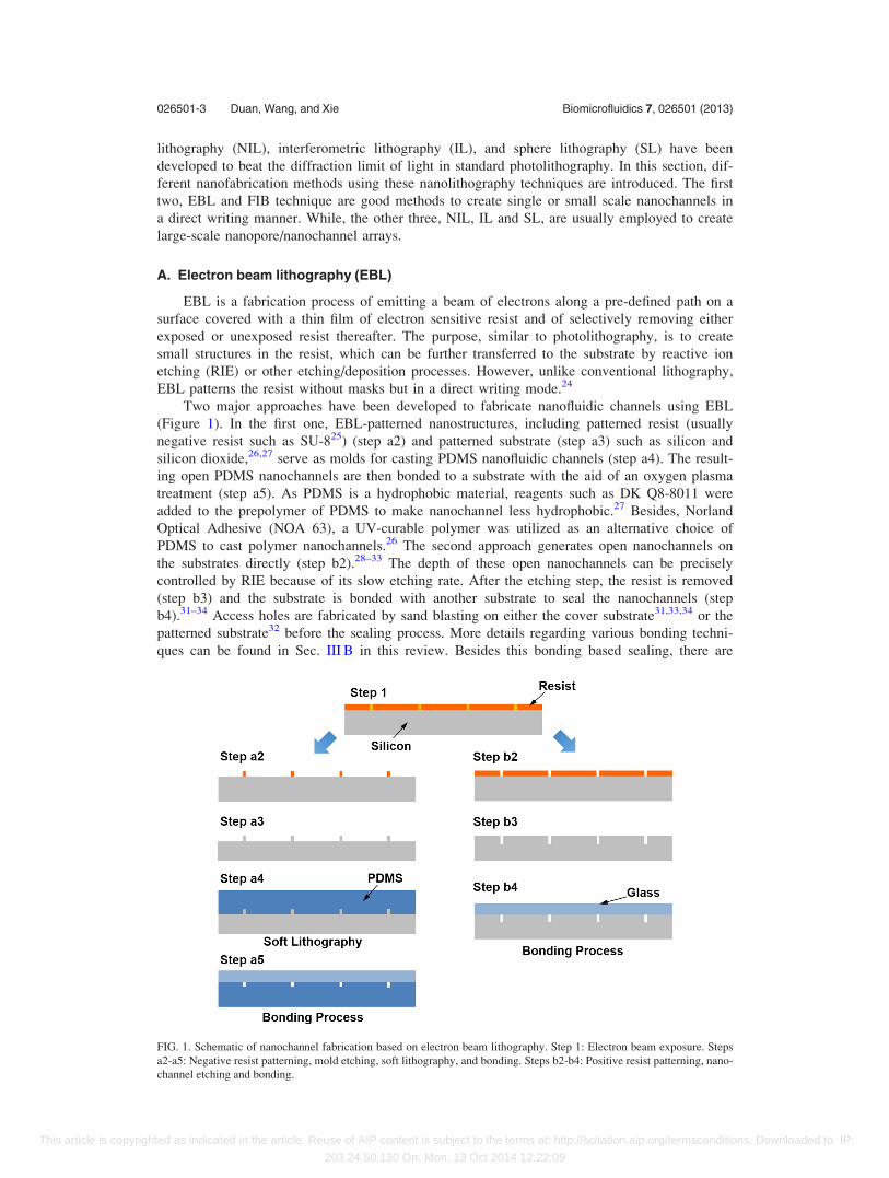
Two major approaches have been developed to fabricate nanofluidic channels using EBL
(Figure 1). In the first one, EBL-patterned nanostructures, including patterned resist (usually
negative resist such as SU-825) (step a2) and patterned substrate (step a3) such as silicon and
silicon dioxide,26,27 serve as molds for casting PDMS nanofluidic channels (step a4). The result-
ing open PDMS nanochannels are then bonded to a substrate with the aid of an oxygen plasma
treatment (step a5). As PDMS is a hydrophobic material, reagents such as DK Q8-8011 were
added to the prepolymer of PDMS to make nanochannel less hydrophobic.27 Besides, Norland
Optical Adhesive (NOA 63), a UV-curable polymer was utilized as an alternative choice of
PDMS to cast polymer nanochannels.26 The second approach generates open nanochannels on
the substrates directly (step b2).28–33 The depth of these open nanochannels can be precisely
controlled by RIE because of its slow etching rate. After the etching step, the resist is removed
(step b3) and the substrate is bonded with another substrate to seal the nanochannels (step
b4).31–34 Access holes are fabricated by sand blasting on either the cover substrate31,33,34 or the
patterned substrate32 before the sealing process. More details regarding various bonding techni-
ques can be found in Sec. III B in this review. Besides this bonding based sealing, there are
FIG. 1. Schematic of nanochannel fabrication based on electron beam lithography. Step 1: Electron beam exposure. Steps
a2-a5: Negative resist patterning, mold etching, soft lithography, and bonding. Steps b2-b4: Positive resist patterning, nano-
channel etching and bonding.
026501-3 Duan, Wang, and Xie Biomicrofluidics 7, 026501 (2013)
This article is copyrighted as indicated in the article. Reuse of AIP content is subject to the terms at: http://scitation.aip.org/termsconditions. Downloaded to IP:
203.24.50.130 On: Mon, 13 Oct 2014 12:22:09

several self-sealing methods to form enclosed nanochannels. It has been reported that EBL pat-
terned open nanotrenches can be sealed by atomic layer deposition (ALD) to form sub 10 nm
channels.35 Bilayer e-beam resist, PMMA/PMGI (polydimethyl glutarimide), is also used for
self-sealing the channel.36 After exposed by EBL, the more sensitive PMGI (bottom layer) is
fully exposed and developed to form the nanochannel, while the PMMA (top layer) leaves a
chain of dot patterns right above the PMGI pattern. Reflowing PMMA produces a polymer
nanochannel with channel width defined by EBL.
As electron beam has a much smaller wavelength than UV light in convectional photoli-
thography, features of 10 nm scale or even smaller can be achieved by EBL. Furthermore, EBL
is ready for further integration with other traditional microfabrication techniques, such as sacri-
ficial layer releasing (SLR),37 to prepare complicated micro/nanofluidic devices. However, EBL
is not a suitable tool for mass production of nanofluidic devices because of its relatively high
cost and low scanning/writing speed.
B. Focused ion beam (FIB) technique
FIB is a technique that utilizes a focused beam of ions to achieve site-specific fabrications,
such as swelling, milling, implantation, ion-induced deposition, or etching, with nanometer re-
solution.38 It is often known as a powerful defect-repair tool in the semiconductor industry.
Recently, FIB, especially FIB milling, attracts great attentions in the nanofabrication because it
is capable of generating specific nanoscale patterns directly on hard substrates without requiring
masks or photoresists. When FIB is operated with a proper beam size, beam current, and energy
(10–100 keV) during a milling process, a cascade of collisions introduced by incoming ions can
provide target atoms enough energy to overcome surface binding and escape from the substrate,
which thereby leaves nanoscale trench in situ.38,39
FIB milling is widely used to fabricate nanopores through thin membranes prepared
by standard microfabrication.40–45 Low stress silicon nitride (SiN) prepared by low pressure
chemical vapor deposition (LPCVD) is the most used membrane material in this approach
(Figure 2).40–43 Gaþ FIB milling is operated to drill nanoscale (�10 nm) openings through the
SiN membrane (step 2). To prevent surface from charging up due to ion implantation and sec-
ondary electrons generation, a metal layer, such as Au and Cr, or conductive polymer is usually
coated onto the SiN layer before the drilling process. Electron beam irradiation is an alternative
method to compensate surface charging effects. After drilling, ALD is applied to further narrow
FIG. 2. Schematic of nanopore/nanochannel fabrication based on focused ion beam technology. Nanopore fabrication: Step
1: Thin film deposition and back chamber etching. Step 2: FIB milling. Step 3: Nanopore shrinkage using isotropic deposi-
tion. Nanochannel fabrication: Option (I) Direct FIB scanning, Option (II) Introduction of a sacrificial layer, followed by
FIB scanning and sacrificial layer etching. The additional sacrificial layer in option II can help remove ridges formed during
FIB scanning.
026501-4 Duan, Wang, and Xie Biomicrofluidics 7, 026501 (2013)
This article is copyrighted as indicated in the article. Reuse of AIP content is subject to the terms at: http://scitation.aip.org/termsconditions. Downloaded to IP:
203.24.50.130 On: Mon, 13 Oct 2014 12:22:09

the nanopores (step 3). The additional Al2O3 layer can also reduce the electrical noise and thus
improve device performance.40 Similarly, electron-beam-assisted silicon oxide deposition41 or
another ultrathin layer of LPCVD SiN deposition43 was carried out to reduce the diameter of
the nanopore (step 3). Besides SiN, other materials including gold,46 aluminum,44 PMMA,45
and PDMS47 have been used to form corresponding functional nanopores by FIB milling as
well.
Another application of FIB in nanofabrication of nanofluidic devices is to generate nano-
channels parallel to the surface using a scanning mode (Figure 2). Nanochannels with feature
size of several tens of nanometers have been successfully fabricated by FIB milling on silicon
substrate,48,49 quartz substrates,50,51 and grown thermal oxide layer52 (option I). Although
etched nanochannels can be sealed by glass wafer through various bonding techniques,52 the
corresponding sealing is not trivial as FIB-milled nanochannels usually have ridges along the
channel banks due to swelling and re-deposition during milling53 (option I). Such ridge struc-
tures can be avoided by introducing a sacrificial layer (a relatively thick metal film) onto the
target substrate before milling and then selectively removing it afterwards (option II). 1-D open
nanochannels with smooth top surfaces and lateral dimensions as small as sub-5 nm were fabri-
cated based on this approach, which were easily sealed with a cover plate.51
FIB technique has also been utilized to fabricate multi-functional micro/nanofluidic devices
on silicon wafers when it was integrated with traditional micromachining processes. For exam-
ple, nanofluidic devices with embedded transverse nanoelectrodes were successfully fabricated
using combined techniques including photolithography, silicon etching, lift off, FIB Pt deposi-
tion, and milling.52 Another example is milling the substrate with predefined microstructures to
prepare hybrid micro/nanoscale molds for soft lithography based micro/nanochannel fabrication,
which can lower down the cost for massive production of nanofluidic devices.54–56
In short, FIB has shown its promise in the fabrication of nanofluidic devices as it can
directly generate nanoscale features on the substrate and is compatible with other fabrication
techniques. Unfortunately, this technique still requires costly equipment and the fabrication
yield is even lower than EBL because of the direct milling/deposition mode.
C. Nanoimprint lithography (NIL)
In addition to the above two direct writing based techniques, NIL is an important nano-
lithography method with high-throughput capability. Unlike conventional lithography, NIL rep-
licates nanoscale features by mechanically pressing predefined molds into imprint resist and
thus overcomes the diffraction limit.57 It has been widely used in recent decades to fabricate
1-D and 2-D nanochannels in varied nanofluidic systems.
As shown in Figure 3, in a typical NIL-based nanochannel fabrication process, a thin layer
of imprint resist is first spun onto the substrate (step 1). A hard mold with predefined nanoscale
patterns is then brought into contact with the substrate and they are pressed together under cer-
tain load (step 2). Subsequently, the resist layer is cured and solidified by heat or UV light. The
pressure and temperature during this imprinting (pressing and curing) step are carefully con-
trolled to achieve robust mechanical deformation of the imprint resist. After the curing process,
the hard mold is removed, leaving the reverse nanostructures on the resist layer (step 3). This
patterned resist can directly function as open nanochannel (step 3) or serve as a mask for pattern
transfer to fabricate the open nanochannel. In the latter case, the residual resist remaining in the
contact area is removed by O2 plasma etching first (step 4) and then another etching step trans-
fers the nanopattern onto the substrate. Similar to other nanolithography-based nanochannel fab-
rication approaches, the NIL-based approach also requires a sealing/bonding step to enclose the
open nanochannels. Direct thermal bonding with polymers including SU-858,59 and PMMA60 has
been utilized as one of the popular sealing/bonding methods. Solvent vapor sealing61 and melting
induced reflowing62 have also served as promising methods in sealing the NIL prepared nano-
channels. In addition, the NIL template itself can be directly used to form enclosed nanochannels
between imprint resist and the template if the deformed imprint resist cannot completely fill the
trench region on the template.63 Although this method is a single-step process for nanochannel
026501-5 Duan, Wang, and Xie Biomicrofluidics 7, 026501 (2013)
This article is copyrighted as indicated in the article. Reuse of AIP content is subject to the terms at: http://scitation.aip.org/termsconditions. Downloaded to IP:
203.24.50.130 On: Mon, 13 Oct 2014 12:22:09

fabrication, the imprinting template cannot be reused thereafter, thus losing the main advantage
of NIL in nanofabrication.
A variety of materials, such as SU-8,58,59 PMMA,60,64 sol-gel silica,65 and some UV cura-
ble polymers,66 have been employed as imprinting resist. In contrast to the various choices for
resist materials, imprint molds are generally made by silicon or quartz because of their stiffness
and process compatibility. Silicon/quartz molds can also avoid thermal expansion mismatch
with substrates in the imprinting process as in most cases substrates themselves are silicon.
Imprint molds used in NIL are generally formed by another nanolithography process (e.g., deep
UV lithography, EBL, or interferometric lithography) followed by a corresponding reactive ion
etching.
NIL can generate nanoscale features (�10 nm) over a large area with relatively low cost
compared with the aforementioned EBL and FIB as its molds can be reused, which makes this
technique promising in high-throughput nanofluidic device fabrication. Another advantage of
the NIL-based nanochannel fabrication is its compatibility with other microfabrication
approaches in terms of forming complicated micro/nanofluidic devices. For example, mixed-
scale structures were prepared by employing NIL on a pre-processed substrate with microstruc-
tures on top.64 Reano and Pang have developed sequentially stacked thermal nanoimprint
lithography on planarized layers to achieve multi-level (3D) nanochannel network on a silicon
wafer.67 Two sequential NIL (Dual-NIL) processes have recently been advanced to fabricate
electrodes over nanofluidic channel for in situ DNA transportation detection.68 Hierarchical
silica nanochannels have also been fabricated by introducing block copolymer thin film tem-
plate.66 In spite of these advantages listed above, NIL may not be a cost-effective nanolithogra-
phy technique when imprints molds are not available or only used for limited times as the
fabrication of the imprints modes requires other expensive nanolithography techniques.
D. Interferometric lithography (IL)
Similar to NIL, IL is a technique capable of fabricating large-area, nanometer-sized, peri-
odically patterned structures.69 In the literature, this technique has been variously referred to as
holographic lithography, or interference lithography. In this technique, a coherent laser source
is split into two different beams and then projected onto the photoresist. Typical sinusoidal in-
terference pattern with certain pitch is formed on the photoresist based on interferometric
FIG. 3. Schematic of nanochannel fabrication based on nanoimprint lithography. Typically, this method includes two major
processes, i.e., nanochannel patterning and nanochannel sealing. The patterning process consists of four steps: Step 1:
Imprint resist coating. Step 2: Mold pressing. Step 3: Mold removal. Step 4: Residual resist etching. Available sealing
options include direct thermal bonding, solvent vapor sealing, melting reflow sealing, and direct template sealing.
026501-6 Duan, Wang, and Xie Biomicrofluidics 7, 026501 (2013)
This article is copyrighted as indicated in the article. Reuse of AIP content is subject to the terms at: http://scitation.aip.org/termsconditions. Downloaded to IP:
203.24.50.130 On: Mon, 13 Oct 2014 12:22:09

exposure of these two coherent beams. The resulting patterning line width is determined by the
incident light wavelength, angle, and developing time. This process is maskless and only relies
on light and material properties. Nanoscale pattern of the photoresist can be transferred to the
substrate via etching process. Up to now, the width of nanochannel immediately after etching
can reach 200 nm and further thermal oxidation may narrow the width down to 100 nm or
smaller.
Researchers have employed this method to fabricate large scale nanochannel array on sili-
con substrate.70–76 IL can also be used to fabricate nanoscale molds, which can serve as masters
for PDMS molding to fabricate PDMS nanochannels.77 In addition, combining with traditional
MEMS techniques, IL has been used to pattern high-density nanopore array with porosity of
approximately 20%.78 Multilayer fluidic platform was achieved by sandwiching this nanopore
membrane with other PDMS microfluidic networks.79 However, IL can only generate nanochan-
nel/nanopore array based on its working principle. The inability to fabricate single nanochan-
nel/nanopore limits its applications in nanofluidics.
E. Sphere lithography (SL)
SL, also named as colloidal lithography, is another low-cost technique to pattern large-
scale two dimensional ordered nanostructure arrays,80–82 especially nanopore arrays. As shown
in Figure. 4, to fabricate a nanopore array based on SL, a close-packed nanoparticle monolayer
is first prepared on a plane substrate (step 1). These close-packed nanoparticles are used as an
etching mask to transfer triangular interstice patterns into the substrate by a subsequent aniso-
tropic etching (step I2).83 Or, they are separated by a controlled reactive ion etching (step II2)
and then covered with metal or other thin film materials (step II3). After releasing the residual
nanoparticles, hole-shaped nanopatterns are left on the substrate, as indicated in step II4. The
nanohole patterns in the deposited film can be directly used as a nanoporous membrane after an
FIG. 4. Basic fabrication process of nanopore array by sphere lithography. After the preparation of a close-packed nanopar-
ticle monolayer (step 1), two fabrication approaches are available and lead to different final structures. Option I: Step I2:
Dry etching the substrate. Step I3: Releasing nanoparticles. Option II: Step II2: Dry etching the nanoparticles. Step II3:
Depositing thin film. Step II4: Releasing nanoparticles. Step II5a: Isotropically etching the substrate. Step II5b: anisotropi-
cally etching the substrate. Substrate with a pre-etched back chamber was used here. The back chamber can also be created
after step I3 or step II5 to form the final structure.
026501-7 Duan, Wang, and Xie Biomicrofluidics 7, 026501 (2013)
This article is copyrighted as indicated in the article. Reuse of AIP content is subject to the terms at: http://scitation.aip.org/termsconditions. Downloaded to IP:
203.24.50.130 On: Mon, 13 Oct 2014 12:22:09

isotropic etching of the substrate (step II5a), or can be further transferred into the substrate
with an anisotropic etching (step II5b). The latter step can be used to form a suspended mem-
brane with a through-nanopore array, once a back chamber is prepared by the traditional micro-
fabrication technique either before the sphere lithography or after.
The key step in the SL based nanofabrication approach is the preparation of a high quality
monolayer of nanoparticles. Most monolayers are formed by classic assembly-based methods,
including evaporation induced self-assembly,84 Langmuir-Blodgett deposition85,86 or roll-to-roll
process.87 Even some of the above methods86,87 have demonstrated their ability in wafer-scale
fabrication, the process compatibility of the assembly-based nanoparticle monolayer preparation
with traditional microfabrication still remains a challenge due to requirements of special instru-
ments and tricky manual operations, which limit the applications of sphere lithography in nano-
fluidics. Recently, monolayer of nanoparticles has been achieved by spin-coating a photoresist
or hybrid sol88 with particles doped. These new methods, in principle, are compatible with tra-
ditional microfabrication processes and thereby hold great potential in developing another use-
ful tool for the fabrication of micro/nanofluidic devices.
III. MEMS BASED NANOFABRICATION APPROACHES
Although nanolithography based approaches can fabricate various nanostructures, the most
popular nanofabrication approaches still rely on standard MEMS techniques due to their high
throughput and low cost, benefiting from the wafer-scale processing ability. These MEMS
based fabrication approaches usually involve structure definition using standard photolithogra-
phy and structure formation via a series of additive (deposition)/subtractive (etching) processes.
Although conventional photolithography tools in a research facility cannot directly define nano-
scale features, precise controls in the well-defined deposition/etching processes can create struc-
tures with depth and/or width in the nanoscale. In the following section, we will introduce five
different MEMS based fabrication approaches. The first two, sacrificial layer releasing and etch-
ing and bonding are usually used to fabricate 2-D planar nanochannels with a low AR. The
other three, including etching and deposition, edge lithography, and spacer technique, are more
suitable for fabricating 2-D vertical nanochannels with a high AR.
A. Sacrificial layer releasing (SLR)
SLR is one of the most popular top-down approaches to fabricate 1-D or 2-D nanochannel
devices. In this process, nanochannels are formed with a nanometer-thick sacrificial layer that
is first used to define the male form of the nanochannel and is then removed in order to open
the aperture21 (Figure 5). Generally, a bottom layer is deposited on the substrate (step 1),
FIG. 5. Schematic of nanochannel fabrication based on sacrificial layer releasing method. Step 1: Deposition of the bottom
layer. Step 2: Deposition of the sacrificial layer. Step 3: Pattern sacrificial layer to create the male form of the nanochannel.
Step 4: Deposition of the capping layer. Step 5: Formation of access reservoirs. Step 6: Nanochannel releasing.
026501-8 Duan, Wang, and Xie Biomicrofluidics 7, 026501 (2013)
This article is copyrighted as indicated in the article. Reuse of AIP content is subject to the terms at: http://scitation.aip.org/termsconditions. Downloaded to IP:
203.24.50.130 On: Mon, 13 Oct 2014 12:22:09

followed by the deposition of a thin sacrificial layer (step 2). After patterning this sacrificial
layer (step 3), a capping layer is deposited to enclose the patterned structures (step 4). The cap-
ping layer is then patterned to make holes for etchant later to access the sacrificial layer (step
5). Finally, the sacrificial layer is removed using a selective etching process to form the nano-
channels (step 6). It is the thickness of this sacrificial layer that determines the height of the
nanochannel. The bottom layer (step 1) is not always required, but is usually introduced to
make the channel of the same material.
The commonly used sacrificial materials are amorphous/polysilicon,3,6,89–95 silicon diox-
ide,96,97 metals,98–105 and polymers.106–114 Among them, amorphous/polysilicon3,5,89–95 and sili-
con dioxide,96,97 were chosen first due to their temperature stability, mechanical rigidity, and
process compatibility with the subsequent deposition processes. The corresponding etchants are
xenon difluoride (XeF2, dry etching of silicon)/tetramethylammonium hydroxide (TMAH, aniso-
tropic wet etching of silicon), and hydrofluoric acid (HF, wet etching of silicon dioxide),
respectively. Metals are also a class of popular sacrificial materials. The high selectivity of the
metal etchant (up to 106:1) between metal and substrate ensures excellent height uniformity
throughout the whole channel. So far, Al,98,99,103 Cr,100–102,105 Ge,94,104 Ti/W,100 Pt,100
Cu,100,105 and Ta100 have been tested to produce nanofluidic channels. In addition to these inor-
ganic materials, several organic polymers, including SU-8,99 Shipley S1805 photoresist,106 poly-
vinyl alcohol (PVA),107 polyethylene oxide,108,109 polynorbornene,112,113 polycarbonate (PC),114
and even DNA110,111 have also been used as sacrificial materials. However, compared with
inorganic materials, there are limited choices of capping materials for these polymers.
Although lots of materials can serve as the sacrificial material, the traditional SLR
approach suffers from slow, diffusion-limited etching, making it difficult to produce long nano-
channels. It has been reported that releasing a 0.66-mm long nanochannel would require 15 h of
etching.3 One way to reduce the etching time is to release the sacrificial layer from its side
instead of from two ends. A subsequent non-conformal deposition, e.g., plasma-enhanced chem-
ical vapor deposition (PECVD), can reseal the channel from the side to prevent leakage.
Because etching from the side is along the channel width direction instead of the channel length
one, this alternative approach could significantly save the etching time. Huang et al. have used
this method to prepare centimeter-long nanochannels within 90 s.115 One drawback regarding
this method is the edge deformation of the capping layer due to stress release during etching.115
Consequently, the cross-section of the final released nanochannel deviates from the originally
designed rectangular shape. This issue becomes less serious when thick capping layer is depos-
ited and/or the etching period is well controlled to have a very short releasing path.104 The lat-
ter case has actually been developed as a new method to fabricate 1-D nanochannels. Hoang
et al. used this method to produce 10 mm-long 1-D nanochannels with a cross-section of
20 nm� 40 nm.116 By carefully controlling the side etching time, Sordan et al. have also created
nanochannels with a cross-section of 10 nm� 10 nm.104 Another alternative approach to shorten
the releasing time is to use new sacrificial materials that are easy to remove. Thermal decom-
posable polymers112–114 were introduced as a new class of sacrificial material for this purpose.
These polycarbonate-based polymers vaporize when they are heated up to certain temperatures
(300–400 �C), yielding short releasing time due to fast gas diffusion. These polymers are also
sensitive to E-beam irradiation and thus could be used as resist for nanoscale patterning and
fabrication of 1-D nanochannels. Despite these advantages, it is worth noting again that there
are limited choices of the capping layers since most deposition of the capping layer has a pro-
cess temperature higher than the glass temperatures of these polymeric sacrificial materials. In
addition to these two approaches above, new etching methods can be applied to speed up the
releasing process. For example, external electric potential has been applied to accelerate gal-
vanic corrosion during the releasing Cu/Cr sacrificial layers.100,105
While SLR is mostly used to fabricate single or a small group of horizontally aligned 1-D/
2-D nanochannels, it also has the potential to form large scale nanofluidic structures. Grattoni
et al. have used sacrificial layer etching to prepare densely packed nanoslits (nanofluidic mem-
branes) with 5.7 nm and 13 nm in height.117 James Lee’s group has combined this technique
with imprinting to form laterally ordered nanochannels arrays using DNA wires as the
026501-9 Duan, Wang, and Xie Biomicrofluidics 7, 026501 (2013)
This article is copyrighted as indicated in the article. Reuse of AIP content is subject to the terms at: http://scitation.aip.org/termsconditions. Downloaded to IP:
203.24.50.130 On: Mon, 13 Oct 2014 12:22:09

sacrificial structures.110,111 They also used a similar approach to prepare conical shaped nano-
pore array with PVA as the sacrificial material.107 Besides horizontal nanochannel array, sacrifi-
cial layer releasing has also been employed to generate vertically aligned nanochannel arrays
by multi-step deposition of sacrificial and capping layers. Shen et al. alternatively deposited
multilayers of silicon nitride (capping layer) and silicon oxide (sacrificial layer) to achieve
nanofiltration structures with minimum channel height of 100 nm.97 Sordan et al. fabricated ver-
tical nanochannel array by selective side etching of a SiGe heterostructure comprised of layers
of alternative Ge fraction.104
In short, compared with other nanochannel fabrication approaches, SLR is relatively simple
and inexpensive, amenable to integration with other microstructures to form integrated micro/
nanofluidic devices and capable of fabricating complicated 3-D nanofluidic structures. The
formed nanochannels are only several microns (or even less) from the device surface, allowing
accurate observation and interpretation of the experiments. However, this surface micromachin-
ing approach has two inherent limitations. First of all, it is difficult to use this approach to fab-
ricate ultrathin nanochannels. Current minimum channel size using this approach is around
10 nm, below which it is difficult to control the thickness of the sacrificial layer and channel
tends to collapse due to capillary force during etchant extraction or liquid introduction. Such
collapsing during releasing can be intentionally introduced to form 1-D nanochannels.94,118
Secondly, etchants and reactants may remain inside the (long) channels after releasing, resulting
in undesirable influence on the subsequent nanofluidics experiments.116
B. Etching and bonding
Another commonly used MEMS fabrication approach for nanofluidic devices is etching and
bonding. In this approach, 2-D planar nanochannels are formed by etching nanometer-deep
trenches in a substrate, followed by bonding it to another plane substrate (Figure 6). Normally,
this fabrication scheme starts with a standard photolithography step on a double-side polished sil-
icon or glass (quartz) substrate. This photolithography is used to define the width and length of
the nanochannel. Using the patterned photoresist as a mask, an etching step is then performed to
form a shallow trench on the substrate (step 1). It is this etching step that determines the final
height of the nanochannel. After this step, similar photolithography and etching are applied again
to create microchannels that are used to introduce liquid and connect other fluidic components
(step 2). The top surface is then deposited with a thick oxide layer using PECVD (step 3). This
layer serves as a protection layer for both microchannels and nanochannels during the subsequent
FIG. 6. Schematic of nanochannel fabrication based on etching and bonding method. Step 1: Nanochannel patterning and
etching. Step 2: Microchannel patterning and etching. Step 3: Deposition of the protection layer. Step 4: Backside reservoir
patterning and etching. Step 5: Removal of the protection layer. Step 6: Uniform growth/deposition of an insulation layer,
e.g., a thermal oxide layer (optional). Step 7: Anodic bonding with a glass substrate.
026501-10 Duan, Wang, and Xie Biomicrofluidics 7, 026501 (2013)
This article is copyrighted as indicated in the article. Reuse of AIP content is subject to the terms at: http://scitation.aip.org/termsconditions. Downloaded to IP:
203.24.50.130 On: Mon, 13 Oct 2014 12:22:09

reservoir formation step (step 4). Reservoirs are patterned from the back side of the wafer and a
deep reactive ion etching (DRIE) or drilling process is employed to create through-substrate
holes. The top oxide layer is removed by HF solution after this step (step 5). The wafer is then
sent into a furnace to uniformly grow thermal oxide on all exposed surfaces (step 6). This re-
oxidation step is not required, but is usually introduced to add an insulation layer on silicon sub-
strate. Finally, this substrate is bonded with another substrate (step 7) after a careful cleaning
process (usually including hot piranha treatment, di-ionized water rinse, and nitrogen blow dry).
As self-explained by its name, there are two major challenges regarding this MEMS-based
nanofabrication approach. The first one is the nanochannel etching. Etching techniques with ro-
bust and high precision control are desired to achieve nanometer-sized depth. The corresponding
etching methods include bulk etching and thin film etching. In bulk etching, the thickness of the
trench is determined by the etching rate along with the etching time. Currently, there are two
bulk etching techniques, dry etching (usually RIE) and wet (chemical) etching. RIE is mainly
used for silicon substrate.13,119–126 The corresponding etching rate can be adjusted by several pa-
rameters in this technique, including gas composition, pressure, power, substrate to electrode dis-
tance, and substrate temperature. Although it was initially believed this technique did not have
precise controllability and often resulted in a rough etched morphology, advanced RIE technique
has showed the ability of etching 2-nm deep trench in silicon with a surface roughness around
0.2 nm.125 Compared with RIE, wet etching does not have any other tuning parameters for the
etching rate except chemical concentration and bath temperature. However, it is much easier to
prepare and does not require any special instruments. Wet etching has been used for both silicon
and glass substrates. In particular, diluted HF and buffered HF (BHF) have been used to etch
glass substrate,127–135 while NaOH/KOH, TMAH, and Olin OPD 4262 (a positive resist devel-
oper) have been used to etch silicon substrate119,136–138 to form desired nanochannels. In contrast
with bulk etching, the depth of the trench in thin film etching is normally predefined by the
thickness of the deposited film (spacer layer) once a highly selective etching method is chosen.
Various materials, including amorphous silicon,139–141 poly-silicon,142 silicon carbide,143 and sili-
con dioxide,118,144–146 have been used as the spacer layer. A special technique under the category
of thin film etching is the double thermal oxide technique. In this technique, a thick layer of
thermal oxide layer is first grown on silicon substrate. The following selective etching defines
the nanochannel horizontal geometry (width and length) and opens a window to expose the
underneath silicon substrate. A second thermal oxidization step is then performed to grow a thin-
ner thermal oxide on the exposed regime. The final height of the nanochannel can be determined
either by the difference between two oxide layers directly147 or the consumptions of silicon dur-
ing the second oxidation on the exposed and unexposed regimes.148–152 This technique benefits
from the precision control of thermal oxide growth and can potentially produce nanochannels
with any specified height. Another special technique of thin film etching is to use native oxide
(�1 nm) as the spacer layer.153 Because native oxide can re-grow in ambient atmosphere, the
selective etching and re-growing can happen several times to get channels with different heights.
6-nm-deep nanochannels have been created by this method.153
Overall, it is no exaggeration to say that current etching techniques are capable of provid-
ing precision down to 1 nm. The real limiting step for the etching and bonding approach is,
thus, the bonding step. Current available bonding methods include anodic bonding, thermal
fusion bonding, as well as adhesion bonding. Anodic bonding is a unique bonding technique
that can generate a permanent chemical bond between silicon and glass substrates. This tech-
nique requires a high DC voltage (�1000 V) to drive O2� ions moving from glass substrate to
silicon substrate to form Si-O bonds at a temperature (� 400 �C). As a result, nanochannels
made by this technique are subject to collapsing due to the strong electrostatic force during
bonding. Typically, for a give channel width w, the minimum channel height (hmin) that is
allowed to avoid collapse follows an expression below:
hmin ¼we0V2
Eef f
� �13
;
026501-11 Duan, Wang, and Xie Biomicrofluidics 7, 026501 (2013)
This article is copyrighted as indicated in the article. Reuse of AIP content is subject to the terms at: http://scitation.aip.org/termsconditions. Downloaded to IP:
203.24.50.130 On: Mon, 13 Oct 2014 12:22:09
where e0 is the dielectric constant, Eeff is the effective Young’s modulus, and V is the applied
voltage.154 One way to overcome this limit is to apply anodic bonding with lower temperature
and lower voltage. Song and Wang have used anodic bonding under a condition of 225 �C and
400 V to create nanochannels that were 6-nm-deep and 3-lm-wide.153 Another alternative
method is to intentionally grow a thick insulation layer on the silicon substrate. This insulation
layer does not only prevent electrical leakage from channel wall but also serves as a big capaci-
tor and thus reduces electrostatic force during bonding.125,136 Mao and Han made channels that
were 25 nm deep and 4 lm wide using this modified anodic bonding method.136 Recently, Duan
and Majumdar further pushed the limit down to 2 nm deep with the introduction of a 500 nm
thermal oxide.125 Thermal fusion bonding is another important bonding method in MEMS. In
this method, two stacked substrates are heated to a high temperature close to their glass transi-
tion point. The strong diffusion and local plastic deformation at the interface result in a strong
physical bonding. Thermal fusion bonding normally takes longer time than anodic bonding and
it only works for substrates with similar thermal expansion coefficients. Otherwise thermal mis-
match issue would arise and lead to cracks or even bonding failure. Collapsing is still an issue
for fusion bonding, although not as critical as for anodic bonding. 20-nm-deep nanochannels
have been achieved using regular glass-glass fusion bonding.136 This technique can be further
improved by using water or manually pressing to pre-bond two substrates together. Haneveld
et al. used such a modified fusion bonding technique and pushed the channel depth limit of
fusion bonding down to 5 nm.155 In addition to these two bonding methods above, adhesion
bonding can also be applied as long as the thickness of the adhesion layer is smaller than the
height of the nanochannel. Sodium silicate has been used as such an adhesion agent.7,135,156 For
example, nanochannels down to 50 nm have been formed using uniformly spin-coated, 20-nm
thick sodium silicate as the adhesion layer.135
In brief, etching and bonding approach is probably the best MEMS based fabrication
approach for 2-D planar nanochannels with small AR. This approach is relatively simple and
cost-effective; flexible for integration with other fluidic/electrical components; capable of fabri-
cating ultra-long, ultra-thin, and ultra-low AR individual 2-D nanochannels as well as compli-
cated micro/nanofluidic networks.150,151,157,158 However, there are two minor disadvantages that
prevent it from being an ideal nanochannel fabrication approach. One is that all current bonding
techniques require extremely clean and defect free surfaces, which adds facility requirements
and results in low bonding yield, especially for the fabrication of ultra-thin nanochannels with
ultra-low AR. Another concern is that the materials used in this fabrication approach may bring
certain application limits: Silicon is not a transparent material and thus may cause background
issue for optical observation; glass can gradually dissolve in aqueous solutions and therefore
channels may not be reliable for long-term operation.10,159
C. Etching and deposition
The nanochannels fabricated by SLR or etching and bonding approaches are mostly 2-D
planar channels with nanometer scale height. There are also MEMS based approaches to fabri-
cate 2-D vertical nanochannels with a nanometer-sized width.
One of the approaches is called etching and deposition. This approach is similar to the
etching and bonding approach in which open trenches are first formed on the substrate using
photolithography and etching. However, instead of forming shallow trenches with nanometer
scale height, relatively deep and straight trenches (�at least several microns in depth) are cre-
ated in this approach using anisotropic etching. A non-conformal deposition step is then
exploited to create self-sealing nanochannels, as shown in Figure 7. Clearly, this non-conformal
deposition is the key step for this fabrication approach and it has two important functions, i.e.,
shrinking the trench width to the nanometer scale and sealing the open trenches. It has been
reported that both chemical vapor deposition (CVD) and physical vapor deposition (PVD) proc-
esses, depending on the operating conditions, can form such non-conformal deposition.160–163
Specifically, Ilic et al. exploited this etching and deposition approach to produce Parylene C
nanochannels down to 100 nm regime based on a Parylene C CVD process.160 Wong et al.
026501-12 Duan, Wang, and Xie Biomicrofluidics 7, 026501 (2013)
This article is copyrighted as indicated in the article. Reuse of AIP content is subject to the terms at: http://scitation.aip.org/termsconditions. Downloaded to IP:
203.24.50.130 On: Mon, 13 Oct 2014 12:22:09

used non-conformal PECVD to seal silicon oxide trenches on silicon wafers with phosphor sili-
cate glass (PSG).161 They then further modified these nanochannels into circular profiled-
nanochannels with diameter ranging from 30 to 2000 nm by reflowing the deposited PSG during
a high-temperature annealing process.161 Mao and Han also used non-conformal PECVD to
seal vertical silica nanochannels with channel width down to 50 nm, which was shrunk by a
conformal thermal oxidization from an initial width of 500 nm.163
Important features of this approach include relatively low fabrication cost and channel self-
sealing. Moreover, as 2-D vertical nanochannels are formed below the surface of the substrate,
in principle, the top surface is available for further integration of other fluidic components or
electronic circuits. This leads to more efficient use of the substrate and improved miniaturiza-
tion of the overall device.20 However, despite of the above advantages, this approach lacks pre-
cise control on the final channel width due to the complicated non-conformal deposition inside
the trench.
D. Edge lithography and spacer technique
Instead of using controlled deposition techniques to shrink the channel width to the nano-
scale, 2-D vertical nanochannels can also be formed using controlled etching. Edge lithography
technique, where nanoscale features are created by well-controlled undercuts, is one of the
representatives164–166 (Figure 8). To prepare 2-D vertical nanochannels, a thin metal layer
(10–100 nm) is first deposited on the substrate and patterned by standard lithography (step 1).
Masked by the photoresist, the metal layer is then isotropically etched by a selective metal
etchant, resulting in nanometer scale undercuts (step 2). Afterwards, a second metal layer with
similar thickness is deposited on the substrate (step 3). A following lift-off process then
removes the photoresist along with the metal layer above (step 4). As a result of this step, a
metal mask with patterned nanogaps is formed on the substrate. This mask is used in the next
DRIE step (step 5) to create deep trench with nanoscale width. Finally, the metal mask is
removed (step 6) and nanochannels can be formed by bonding or deposition methods (step 7),
similar to what have been introduced in Sec. III B and III C. This technique can also be modi-
fied to prepare nanometer-sized molds to make vertical PDMS nanochannels.165
Currently, two types of metals, chromium and aluminum, have been used to form the
mask with nanogaps for the following DRIE. Other metals and materials can replace these
two metals as long as there are corresponding selective and controllable etchants. The typical
width of the nanogaps and the resulting nanochannels is around 50–200 nm, which is limited
by the undercutting controllability. However, this width can be further reduced by uniformly
FIG. 7. Schematic of nanochannel fabrication based on etching and deposition method. Non-conformal deposition results
in self-sealing nanochannels.
026501-13 Duan, Wang, and Xie Biomicrofluidics 7, 026501 (2013)
This article is copyrighted as indicated in the article. Reuse of AIP content is subject to the terms at: http://scitation.aip.org/termsconditions. Downloaded to IP:
203.24.50.130 On: Mon, 13 Oct 2014 12:22:09

growing another material onto the trenches after removal of the metal mask.165 For silicon
substrates, this can be done by controlled thermal oxidization. Xie et al. have used this
method to further shrink the channel width and produced wafer-scale 2-D high-AR vertical
nanochannels.167
Another approach that employs controlled etching to fabricate vertical nanochannels is
based on spacer technique.168 In this approach, the nanoscale width of the nanochannels is
defined by the thickness of the spacer layer.169–171 The process is schematically illustrated in
Figure 9. As the first step, a standard photolithography is used and followed by anisotropically
etching the substrate to form vertical trenches with micrometer sized openings. The height of
these vertical trenches determines the final height of the nanochannels. Afterwards, a thin
spacer layer is uniformly deposited on the substrate using CVD technique (step 2). Vertical ani-
sotropic etching is then performed again on the substrate (step 3). This etching step removes all
the deposited spacer materials except those at the sidewalls of the trenches, which will serve as
the male form of the vertical nanochannel. Subsequently, a thick capping layer is deposited on
the substrate to cover the sidewall spacer and fill out the vertical trenches (step 4). Chemical-
mechanical-polishing (CMP) is then used to planarize the surface until the sidewall spacer layer
is exposed again (step 5). Finally, a selective etching step is applied to remove the spacer to
form open vertical nanochannels.
These nanochannels can be used as vertical nanochannel membrane directly (step 6I).
Smith et al. fabricated such membrane structures with nanochannel feature width of 5–100 nm
and used them to separate endotoxin from deionized water.169 They can also be sealed by bond-
ing or deposition techniques for other lab-on-a-chip applications (step 6II). Lee et al. used
evaporated gold layer and PECVD silicon oxide to create sealed vertical nanochannels with fea-
ture width down to 25 nm.170 It is worth noting that CMP is not a required step to ultimately
remove the spacer layer. In fact, sacrificial layer releasing can be implemented as an alternative
to form seal nanochannels once the capping layer is deposited (step 6III). Tas et al. fabricated
1-D nanochannels that are 40 nm in width and 90 nm in height using this method.171
There is no doubt that fabrication approaches based on edge-lithography and spacer techni-
ques provide new methods to create 2-D vertical nanochannel structures, which otherwise could
only be formed by expensive nanolithography based approaches (e.g., EBL and NIL) before.
However, these two approaches still cannot completely replace nanolithography based
approaches as the density of the nanochannels, determined by the space between nanochannels,
is still limited by optical lithography.
FIG. 8. Schematic of nanochannel fabrication based on edge lithography technique. Step 1: Deposition and patterning of
the first metal layer. Step 2: Formation of undercuts using isotropic etching. Step 3: Deposition of the second metal layer.
Step 4: Photoresist lift-off. Step 5: Formation of open nanochannels using DRIE. Step 6: Removal of the metal mask. Step
7: Nanochannel sealing using deposition (7 I) or bonding (7 II).
026501-14 Duan, Wang, and Xie Biomicrofluidics 7, 026501 (2013)
This article is copyrighted as indicated in the article. Reuse of AIP content is subject to the terms at: http://scitation.aip.org/termsconditions. Downloaded to IP:
203.24.50.130 On: Mon, 13 Oct 2014 12:22:09

IV. NANOMATERIAL BASED NANOFABRICATION APPROACHES
With the rapid development of nanotechnology, a variety of chemical substances or materi-
als, so-called nanomaterials, with morphological feature size at nanoscale have been synthesized
or manufactured. Recently, using these nanomaterials to prepare nanofluidic devices has
become a popular fabrication strategy. Various nanomaterials, from molecular-scale porous ion
selective polymers to nanoporous membranes, and from 0-D nanoparticles to 1-D nanowire and
nanotube, have been used to prepare nanofluidic devices by taking advantages of their essential
nanometer-size features. This section will review recent achievements in the preparation of
nanofluidic devices based on this idea.
A. Ion selective polymer
Ion selective polymers are chemical substances having a network shaped backbone with
fixed ionic groups tailored and molecule-sized pores inside. When in contact with electrolytes,
these ionic groups will attract counter ions, but repel co-ions from entering this nanoporous
structure as a result of electrostatic interaction in the nanoscale confinement. Although their
regular application is focused on large-scale water pretreatment in a form of membrane, ion
selective polymers are now expanding to construct nanofluidic devices by different patterning
approaches.
The most straightforward patterning method to prepare nanofluidic devices with ion selec-
tive material is based on traditional contact photolithography. For example, through sequential
lithography and etching processes, cation-selective polymer, over-oxidized poly(3,4-ethylene-
dioxythiophene) poly(styrenesulfonate) (PEDOT:PSS), and anion selective material, quaternized
and cross-linked poly(vinylbenzylchloride) (PVBC), were integrated into a single device to real-
ize ion bipolar junction transistors and chemical logic gates.172,173 This contact lithography pat-
terning approach can guarantee a high resolution but requires the ion selective polymers being
of solid and compatible with chemicals used. Alternatively, lithography can be applied on pre-
polymer to realize patterns of certain ion selective polymers when they are UV-curable essen-
tially or become UV-curable with additive photoinitiators. However, this approach faces a
FIG. 9. Schematic of nanochannel fabrication based on spacer technique. Step 1: Patterning and etching of vertical trenches
with micrometer sized openings. Step 2: Deposition of the spacer layer using CVD technique. Step 3: Vertical anisotropic
etching to form the male form of nanochannels. Step 4: Deposition of the capping layer. Step 5: Surface planarization using
CMP. Step 6: Nanochannel formation. Option I. Fabrication of nanochannel membrane by selectively etching nanochannels
and back reservoir. Option II. Fabrication of sealed nanochannels using etching and bonding/deposition technique. Option
III. Fabrication of sealed nanochannel using sacrificial layer etching. Step 5 is not required in this process.
026501-15 Duan, Wang, and Xie Biomicrofluidics 7, 026501 (2013)
This article is copyrighted as indicated in the article. Reuse of AIP content is subject to the terms at: http://scitation.aip.org/termsconditions. Downloaded to IP:
203.24.50.130 On: Mon, 13 Oct 2014 12:22:09
serious contamination issue caused by the possible adhesion between the un-cured prepolymer
and the mask during contacts in traditional lithography. Several non-contact lithographic strat-
egies have been advanced to address this problem. For instance, poly (2-acrylamido-2-methyl-1-
propanesulfonic acid) (PAMPS), a positively charge selective hydrogel, was polymerized in situby an optofluidic maskless lithography system to form a cation-selective filter between two
microchannels for sample preconcentration.174 Similarly, heterogeneous nanoporous junctions
were achieved by patterning cation-selective hydrogel precursors, such as 2-hydroxyethyl meth-
acrylate-acrylic acid (HEMA-AA)175 or AMPS,176 and anion selective ones, like 2-(dimethyla-
mino)-ethyl methacrylate (DMAEMA)175 or (diallyldimethylammonium chloride) DADMAX176
in a non-contact lithographic platform with the help of corresponding photoinitiators.
Microfluidic patterning approach has also been used to pattern ion selective polymer by filling the
ion-selective resin in a tentative PDMS microfluidic channel. After drying the resin for 12 h under
ambient conditions and removing the PDMS channel, ion-selective microelectrodes were pre-
pared for electrochemical activation and inhibition of neuromuscular systems.177 Although these
non-contact lithography techniques can partially solve the contamination issue that traditional
photolithography faces during patterning prepolymers, their spatial resolutions are still limited,
which may block their application in the future large-scale integration of micro/nanofluidics.
Among all the ion selective polymers used in nanofluidics, Nafion, a sulfonated
tetrafluoroethylene-based fluoropolymer-copolymer discovered by DuPont in the late 1960s, is
the mostly used and commercially available proton-selective material. This material has been
extensively used in fuel cell,178 sea water desalinization,15 and highly selective nanofluidic ion
channels. To fabricate a nafion based nanofluidic device, a facile approach is infiltrating resin-
type nafion between gaps created by mechanically cutting the PDMS substrate.15,179 Another
way was patterning a very thin nafion resin layer with thickness of hundred nanometers by ei-
ther stamping180,181 or microfluidic patterning180,182–185 approaches on the substrate. Besides
the above two approaches using nafion resin, thin film typed nafion, which is also off-the-shelf,
was also manually assembled with PMMA microstructures to generate electroconvection and
concentration polarization zone for a high throughput pressure-driven micromixer.186
B. Nanoporous material
Nanoporous materials, which have large porosity (usually greater than 0.4) and pore diameter
between 1 and 100 nm, have been used to construct nanofluidic devices for both fundamental
studies and large-scale applications because of their high surface to volume ratio, ordered and
uniform pore structure, versatile and rich surface composition and properties.187 In this
sub-section, we will introduce several nanoporous materials including 1-D nanoporous membrane
and 3-D nanoporous matrix, and show how to prepare different nanofluidic devices from these
materials.
Anodized aluminum oxide (AAO) is one of the widely used and commercial available 1-D
nanoporous membranes. As shown in Figure 10(a), AAO membrane contains a high density of
uniform cylindrical pores that are aligned perpendicular to the surface and penetrate the entire
thickness of the membrane. AAO is usually formed when aluminum is electrochemically oxi-
dized (anodized) in certain solutions.191 Alumina, the material of AAO, is positively charged
when in contact with aqueous solution and is ready for biomolecule adsorption192 or chemical
modification.193–195 Because of the unique nanoscale structure and surface property, AAO is
very suitable for high throughput nanofluidic applications, such as low-voltage electroosmosis
pump,188,196,197 thin film interference spectroscopy sensing,196 protein filtering,195,198 DNA
sensing,193,194 and large-scale gate-all-around nanofluidic field effect transistors.199 Generally,
AAO membrane used in the nanofluidic study has nanopore diameter of ten nanometers or
larger, and membrane thickness of micrometers. To further reduce the opening pore size, con-
trolled grazing angle Arþ ion milling has been applied to sculpture the U-shaped bottom, which
is usually formed in the so-prepared AAO nanochannels, and obtained the pore aperture down
to 10 nm or below.200 Very recently, by finely controlling the anodization process, AAO tem-
plates with sub-10 nm pore diameters have been successfully prepared.201 Besides the pore size,
026501-16 Duan, Wang, and Xie Biomicrofluidics 7, 026501 (2013)
This article is copyrighted as indicated in the article. Reuse of AIP content is subject to the terms at: http://scitation.aip.org/termsconditions. Downloaded to IP:
203.24.50.130 On: Mon, 13 Oct 2014 12:22:09

distribution of nanopores in AAO can also be tuned by controlled anodization after introducing
pre-defined nanopatterns by EBL,202 FIB direct writing,203,204 or FIB lithography205 at the very
beginning. Moreover, nanochannels in an AAO membrane can be selectively closed and reop-
ened by tuning the FIB beam energy from 30 keV to 5 keV,206,207 which is able to isolate indi-
vidual nanochannel for quantitative nanofluidic study.
Track etched nanoporous membrane, shown in Figure 8(b), is another widely used 1-D
nanoporous membrane in nanofluidics. This material is usually prepared in a polymer mem-
brane by chemically etching the damage trails caused by heavy ion radiation.208–211 Briefly, sin-
gle swift heavy ion beams (MeV per nucleon) from accelerators generate latent tracks through
polymer membrane. A corresponding chemical etching, either one-side etching with the help of
electrostopping technique212 or surfactant-assisted etching,213 removes the damage zone of the
latent tracks and leaves hollow structures through the membrane. The resulting nanopores can
be either funnel, bullet, or cone-shaped by tuning radiation ion source, substrate polymer, etch-
ing method and condition.214 They have been demonstrated in both array and single nanopore
forms in three different polymer membranes including PC,215–219 polyethylene terephthalate
(PET),17,189,209,220–227 and polyimide (PI).214,228,229 Each of these three track etched membranes
has its own advantages. PC membranes with track etched sub-10 nm in diameter nanopores are
commercially available right now and have been used for separation purpose.217 Nanopores fab-
ricated in PET foil exhibit a high surface charge density as well as excellent surface modifica-
tion ability,220,223 which make them a good model for asymmetric electrokinetics study such as
nonlinear ionic current rectification220,222 and oscillations.17 Because of the good chemical sta-
bility of polyimide, track-etched nanopores in polyimide usually have a constant ionic current
readout in various electrolytes, which have been used for bio-sensing225,228 and ionic device230
applications.
In addition to the above two 1-D nanoporous materials, 3-D nanoporous matrix prepared
by a so-called block-copolymer (BCP) approach has also been reported (Figure 10(c)).231 For
example, by selectively removing the amorphous phases in the crystallized polyethylene/
polystyrene (PS) di-block copolymer, a nanoporous membrane with thickness of several micro-
meters and pore size controllable from 5 to 30 nm was prepared.190 Surface properties of nano-
pores prepared by this chemical approach can be precisely tuned, which is important for further
FIG. 10. Typical SEM photos of various nanoporous materials, top: top-view; bottom: cross-sectional view. (a) AAO mem-
brane. Reprinted with permission from Vajandar et al., Nanotechnology 18(27), 275705 (2007). Copyright 2007 Institute
of Physics. (b) Track etched nanoporous membrane. Reprinted with permission from Ali et al., ACS Nano 33, 603–608
(2009). Copyright 2009 American Chemical Society. (c) BCP nanoporous matrix. Reprinted with permission from Uehara
et al., ACS Nano 34, 924-932 (2009). Copyright 2009 American Chemical Society.
026501-17 Duan, Wang, and Xie Biomicrofluidics 7, 026501 (2013)
This article is copyrighted as indicated in the article. Reuse of AIP content is subject to the terms at: http://scitation.aip.org/termsconditions. Downloaded to IP:
203.24.50.130 On: Mon, 13 Oct 2014 12:22:09

biological/chemical functionalization. For example, block copolymer with terminal of di-COOH
group was used to prepare nanoporous membrane for the discrimination of DNA targets with a
single-base mismatch.232 Presently, the biggest concern of applying BCP in quantitative nano-
fluidic study is its irregular pore shape, as shown in Figure 10(c).
Overall, nanoporous materials provide excellent nanoscale confinement, but assembling
them with microstructures to form an applicable nanofluidic device relies on heavy manual
operations, which are time-consuming, non-compatible with traditional MEMS technique, and
difficult in establishing an integrated multi-functional micro/nanofluidics. Recently, it has been
explored by in situ anodizing and etching aluminum film deposited on top of a silicon wafer,
which will definitely expand the applications of AAO in more powerful integrated micro/
nanofluidics.198,233,234 A facile and MEMS compatible process was also developed to prepare
nanoporous structure by involving a solvent-extraction process in the lithography of a regular
photoresist, such as SU-8,235 which may open a new strategy for applying nanoporous materials
in Nanofluidics study.
C. Nanoparticle crystal
Thanks to the rapid development of nanoparticle synthesis in the past decades, monodis-
persed nanometer-sized particles with various surface functional groups have been commer-
cially available. Self-assembly of nanoparticles into well-organized nanostructures, usually
called as nanoparticle crystal, photonic crystal, or synthetic opal as well,236 has been considered
as a valid structured nanomaterial preparation method for different applications including pho-
tonic information237 and Bragg diffraction based biological/chemical sensors.238 Nanoparticle
crystal can also be used as a template to replicate the long-ranged ordered structure into another
solid matrix, called as inversed opal, by filling the interstices and then releasing the particles.239
Other than its original optical applications, nanoparticle crystal has recently been proposed as a
nanoporous matrix for various electrophoresis separations240–242 and sensing243 by utilizing the
steric effects. More interestingly, Chen et al. demonstrated for the first time that interstices in a
self-assembled nanoparticle crystal formed a three dimensional nanochannel network in a FCC
form which had the same electrokinetic property as a single nanochannel but with an enlarged
electrical readout.244 This presented a new perspective on nanoparticle crystal’s application in
nanofluidics. In a simple analogy to a nanotube, the equivalent diameter of the 3-D nanoscale
interstice confined by neighbored nanoparticles can be estimated as 23.38% of the packed parti-
cle diameter.244 To form a nanoparticle crystal in a microchannel, an evaporation-assisted strat-
egy has been reported, as shown in Figure 11. The evaporation induced self-assembly240,244
starts with loading nanoparticle suspension, usually nanoparticles in water or ethanol, into one
reservoir of the microchannel, as shown in steps 1 and 2. Surface tension then drives the
FIG. 11. Schematic of nanofluidic devices fabricated by self-assembling nanoparticles. Step 1: Fabrication of microchan-
nels with reservoirs on both ends. Step 2: Introduction of nanoparticle suspension from one reservoir. Step 3: Self-assembly
of nanoparticle crystal based on capillary evaporation. Step 4: Removal of extra nanoparticles by exchanging the buffer
solution.
026501-18 Duan, Wang, and Xie Biomicrofluidics 7, 026501 (2013)
This article is copyrighted as indicated in the article. Reuse of AIP content is subject to the terms at: http://scitation.aip.org/termsconditions. Downloaded to IP:
203.24.50.130 On: Mon, 13 Oct 2014 12:22:09

meniscus moving forwards until the meniscus stops at the connection between the microchannel
and another reservoir due to the sudden-expansion of the flow duct, as indicated in step 3,
exactly the principle of a capillary valve.245 Without extra input power, the meniscus tends to
keep its shape and position. The continuous evaporation of solvent then leaves nanoparticles
packed from the meniscus. During this process, the inlet is usually covered by a PDMS sheet
to prevent evaporation. The assembly process can be stopped by replacing the nanoparticle sus-
pension in the inlet with suitable buffer solution. Finally, buffers are loaded into two reservoirs
for corresponding nanofluidic study, shown in step 4. Recently, some novel approaches have
reported to pack nanoparticles into designed patterns using PDMS stamping246 or inkjet print-
ing,247 which can further explore the applications of nanoparticle crystal in the nanofluidics
study.
Nanofluidic devices made by this nanoparticle packing approach can easily change surface
properties by modifying or replacing the nanoparticles, showing promise in electrokinetics-
based biosensing applications and fundamental studies. As a proof-of-concept experiment, Lei
et al. reported an nM-level biotin detection by assembling streptavidin modified nanoparticles
(540 nm) in a suspended micropore.248 By packing nanoparticles with different surface
charges249 or diameters250 in a suspended micropore structure sequentially, nanofluidic diodes
were achieved. Another typical nanofluidic electrokinetic phenomenon, ion concentration polar-
ization, was also realized by self-assembling nanoparticles in a microchannel.246
Assembling nanoparticles to construct nanofluidic device has many advantages, such as
low cost, simple and fast fabrication process; large effective cross-sectional area, i.e., large
electrical readout; and more importantly, mature surface modification methods, which make it
easy to graft probes onside for versatile biosensing. It can be foreseen that nanoparticle crystal
will get more and more attentions in nanofluidics, especially in its biosensing applications.
However, self-assembly nanoparticles in a microstructure still need extra efforts to improve
their overall size-controllability and crack-free integrity, which are important for robust sensing
performance and high batch-to-batch repeatability. Recently, Zeng et al. used multiple evapora-
tion microchannels to avoid the drying-induced cracks during the colloidal crystallization and
formed a large scale nanoparticle crystal in microdevice.242 Meanwhile, electrokinetics of the
three-dimensional nanochannel network inside the nanoparticle crystal needs further studies to
provide a more precise and fundamental understanding. Using smaller nanoparticles may not be
as straightforward as it looks, although it could realize a much smaller feature size and thereby
work at a relatively high ionic concentration. Initial wetting of nanoparticle crystal with particle
diameter less than 100 nm could be a big issue and will still require reliable solutions.
D. Nanowire and nanotube
Being two widely used 1-D nanomaterials, nanowires and nanotubes have been employed
to fabricate different nanochannels for a long history. Nanowire can function as either a tem-
plate251 for hot embossing based replication (Figure 12(a)) or a sacrificial master for
molding252–254 (Figure 12(b)) and lithography255,256 (Figure 12(c)) based nanofabrications.
When used as templates, high-hardness nanowires dispersed on a stiff substrate are first
embossed into certain polymer (polycarbonate for example), as shown in Figure 12(a) step 1.
The polymer replicate is then separated from the nanowires (step 2) and bonded to another sub-
strate with predefined microchannels onside to form the final micro/nanofluidic device (step 3).
When used as sacrificial masters, nanowires that can be selectively etched (e.g., silver or zinc
oxide,253 electrospun polyvinylpyrrolidone (PVP),254 etc.) are usually more preferred. These
nanowires can be assembled on top of pre-patterned microstructures to function as masters for
various polymer replications, as shown in Figure 12(b) (step 1). After releasing the nanowire
along with the microstructures embedded in the replica in corresponding etching bathes, poly-
mer micro/nanochannels are obtained, as shown in Figure 12(b) (steps 2, step 3). Alternatively,
one can disperse these nanowires on plain substrates first (Figure 12(c), step 1) and then use
traditional MEMS techniques including thin film coating/deposition, photolithography and etch-
ing to create all related microfluidic components (step 2), and release the nanochannels
026501-19 Duan, Wang, and Xie Biomicrofluidics 7, 026501 (2013)
This article is copyrighted as indicated in the article. Reuse of AIP content is subject to the terms at: http://scitation.aip.org/termsconditions. Downloaded to IP:
203.24.50.130 On: Mon, 13 Oct 2014 12:22:09

(step 3). This approach is very similar to the SLR method that we have introduced in Sec.
III A. Photoresist255 or other deposited materials, such as silicon oxide256 has been used as the
capping layer. Usually, nanowire based nanofabrication presents circular cross-sectional chan-
nels for nanofluidics applications. Nevertheless, some synthesized nanowires presented an ortho-
hexagonal cross section, which can thereby be used to fabricate non-circular nanochannel.255 In
addition, electrospinned polymer nanofibers are used to prepare nanofluidic channel with an el-
liptical cross section188 or a U-shaped cross-section.257
Compared with nanowires, varied nanotubes have been directly used as nanofluidic chan-
nels by assembling them within a membrane258,259 (Figure 13(a)) or bridging them between
two microchannels260–263 (Figure 13(b)). Hinds et al. first reported a nanoporous membrane
FIG. 12. Schematic of nanochannel fabrication using nanowires. (a) Hot embossing based nanochannel fabrication. Step 1:
Hot embossing with nanowire (NW) as master. Step 2: Removing the nanowire. Step 3: Bonding to substrate with prede-
fined microchannels; (b) molding based nanochannel fabrication. Step 1: Assembling nanowire onto microstructures. Step
2: Casting polymer. Step 3: Releasing/removing the nanowire and microstructures and bonding with another substrate; and
(c) lithography based nanochannel fabrication. Step 1: Assembling nanowire on the wafer. Step 2: Patterning photoresist.
Step 3: Releasing nanowire and bonding with another substrate.
FIG. 13. Schematic of nanochannel fabrication using nanotubes. (a) Suspended nanotube membrane. Step 1: Growing
nanotubes (NTs). Step 2: Filling nanotubes with supporting material. Step 3: Releasing the NTs-embedded polymer mem-
brane and opening the nanotubes; (b) nanotube embedded micro/nanofluidic device. Step 1: Growing nanotube on top of
wafer. Step 2: Patterning photoresist or other protecting layer by lithography. Step 3: Opening the nanotube and packaging
the structure with another wafer.
026501-20 Duan, Wang, and Xie Biomicrofluidics 7, 026501 (2013)
This article is copyrighted as indicated in the article. Reuse of AIP content is subject to the terms at: http://scitation.aip.org/termsconditions. Downloaded to IP:
203.24.50.130 On: Mon, 13 Oct 2014 12:22:09

fabrication strategy by encapsulating vertically grown carbon nanotube (CNT) array with poly-
mer.258 Briefly, as shown in Figure 13(a), nanotubes are grown on top of the substrate vertically
(step 1), and then filled with corresponding polymer (step 2). After releasing the polymer with
nanotubes inside and opening the nanotube ends, a CNT membrane is formed (step 3). Besides
CNT, inorganic nanotubes can also be used to form a nanotube-embedded membrane with the
help of microfabrication technique.264 Lithography based patterning on horizontally oriented
nanotubes with different protecting materials, such as PMMA resist262 and silicon ox-
ide,260,261,263 is another fabrication strategy for inorganic nanotube integrated micro/nanofluidic
device, as illustrated in Figure 13(b). Here, nanotubes are grown or dispersed on top of the sub-
strate horizontally (step 1). A protecting layer is deposited and subsequently patterned using
photolithography and etching as illustrated in step 2. After packaging the substrate with corre-
sponding material and opening the nanotube ends, a nanotube based micro/nanofluidic device is
obtained (step 3). Moreover, nanotube has also been molded to form a nanochannel with a pro-
cess similar to Figure 12(b) by replacing nanowire with corresponding CNT.265 More recently,
fluid flow inside nanotube was experimentally measured by directly loading water into CNT
without any capping or protection layer.266 Details on nanotube-based nanofluidic study can be
found in some excellent reviews.267,268
Owing to the rapid development of synthesis techniques of 1-D nanomaterials, using nano-
wire or nanotube to construct nanofluidic device is relatively simple and, in a sense, low-cost.
This strategy is capable of fabricating 1-D nanochannels with uniform surface properties and
feature size ranging from sub-1 nm266 to several tens of nanometer or even larger. It can also
form heteostructured 1-D nanochannels with distinctive surface properties along the channel.
For example, a longitudinal heterostructured SiO2/Al2O3 nanotube was prepared for ionic cur-
rent rectification study.261 Currently, alignment between nanowire/nanotube and microstructures
is the most challenge issue in this nanofluidic device fabrication strategy. Several alignment
methods have been reported, such as using direct mechanical manipulation,251,255 dielectropho-
resis arrangement,265 random dispersion,253,259,262 and directional in situ electrospinning188,254
or growth.260,261,263,266 However, none of them can be as robust and high throughput as the tra-
ditional maker-based optical alignment. For CNT-based nanofluidic devices, there is another
fabrication issue regarding opening the tube end for sample loading. Oxygen plasma etching is
the major method262,263,265 but this method is lacking of precise control and may overetch
CNTs. Recently, it has been reported that electrical breakdown of carbon nanotube under water
droplet was able to open the tube in situ for fluid flow experiments,266 which may present a
new choice to prepare compact and controllable CNT nanofluidic devices.
V. OTHER METHODS
In addition to the above three main nanofabrication strategies, some interesting chemical
properties, physical phenomena, and biological structures have been harnessed to construct
nanofluidic devices. Although these unconventional approaches usually fail to present a reliable
controllability on channel geometry and size, they do provide alternative solutions for the prep-
aration of nanofluidic devices and, in most cases, are even simpler and cheaper than nanofabri-
cation methods we introduced above.
Organic polymers are unstable to UV exposure, easy to crack under stress and deform with
loads. These properties can be utilized to create nanochannel-shaped structures for nanofluidic
devices. It has been reported that certain polymers, including PC269,270 and PMMA,271 decom-
pose upon UV exposure and leave nanoscale structures on the surface. This phenomenon has
been developed as a new sculpturing method to produce 1-D nanochannels. Meanwhile, stress-
mismatch-induced nanometer-sized cracks on some polymers surface, such as PDMS272,273 and
PS,274 formed by mechanical stretching or thermal annealing have been proposed to function as
nanochannels. These nanoscale cracks can be as small as 20 nm in depth274 and are able to con-
nect with microchannels to form integrated micro/nanofluidic devices.273 Similar cracks were
also found in printed toners after being electrically broken down and were used to bridge two
microchannels for nanofluidics based protein preconcentration.275 Moreover, nanochannel
026501-21 Duan, Wang, and Xie Biomicrofluidics 7, 026501 (2013)
This article is copyrighted as indicated in the article. Reuse of AIP content is subject to the terms at: http://scitation.aip.org/termsconditions. Downloaded to IP:
203.24.50.130 On: Mon, 13 Oct 2014 12:22:09
structures can be created based on polymer deformation. Taking advantages of the excellent
thermal plasticity property of PMMA, nanochannels with width down to 132 nm and depth of
85 nm were formed by shrinking pre-prepared PMMA microchannels in a thermal compression
process.276
Besides utilizing special properties of polymers, in certain conditions, failures in traditional
microfabrication can be converted as new methods for nanochannel fabrication. One of the
examples is interstices of polycrystalline grains formed inside thin films during a controlled
CVD277,278 or PVD.279 These interstices usually at sub-10 nm scale have been used as nano-
sieves for protein separation. Another example is nanoscale fractures on fused silica microtube
generated around a scratch either by manually pushing the scratch point or using a supersonic
probe. Nanofractures with feature sizes from 11 nm to 250 nm were formed by this method and
used for DNA preconcentration.280 In addition to these two cases, bonding failures during
PDMS-glass bonding have been explored. It has been reported that insufficient bonding between
plain PDMS and glass substrates may leave nanometer-sized gaps that can be successfully uti-
lized for protein preconcentration.281,282 It has also been shown that the so called “roof
collapse” of PDMS deformation during bonding of PDMS microchannels with large width to
depth ratio (small AR) can generate triangular-shaped nanochannels with feature size around
hundred nanometers at the edge.283 Similar nanochannels were also formed by replicating pro-
tein deposit from confined solution evaporation in deformed PDMS microchannels.284
As another nanochannel preparation strategy, more recently, traditional microscale, or even
macroscale, machining techniques have been expanded to achieve nanoscale structures. It is
well known that glass or quartz capillaries can be pulled with a laser-equipped pipet puller into
microcapillaries. This technique has been improved to realize nanometer-sized capillaries with
the feature size down to 45 nm.285 Coincidentally, materials processing with femtosecond laser
pulses, a widely used micromachining method in optics, has been modified to ablate metal thin
film to form nanochannels with feature size of hundred nanometers.286 Besides these microma-
chining methods, injection molding technique for mass production of disposable all-polymer
devices in traditional machining industry has been optimized to demonstrate an ability in fabri-
cation of nanochannels with width down to 140 nm and depth of 150 nm.287
In addition to the above attempts, nanofluidic devices, nanopores in particular, can also be
realized by utilizing pore-forming proteins. These mushroom or cylinder shaped protein mole-
cules have a nanometer-sized hollow core and thus can be used as nanopores directly after
being inserted in a lipid bilayer membrane. The most widely used pore-forming protein is a-
Hemolysin, a monomeric, 33 kD, 293-residue protein that is secreted by the human pathogen
Staphylococcus aureus.288 a-Hemolysin can be modeled as a nanotube with 10 nm in length
and 1.4–4.6 nm in diameter289 and has found great potential in single biomolecule detection and
analysis, including DNA/RNA sequencing,290 protein/microRNA detection,291–293 and kinetic
studies.294 Beyond a-Hemolysin, several other proteins, including OmpF295 and MspA296 porins
have also been investigated as nanopores for similar applications. Recently, ringlike Stable
Protein 1 and its derivatives have been assembled to form hydrophilic nanochannels in the
plasma membrane of living cells and ohmically link the cell interior and the electrical sensing
pads for neuroelectronic study.297 All these protein-based nanopores/nanochannels mentioned
above, along with other pore/channel forming proteins298 have well-defined nanoscale confine-
ment and excellent reproducibility. However, compared with solid state counterparts, they can-
not be designed at will, and lack durability due to the fragile nature of the supporting lipid
bilayers.
VI. MATERIAL AND FABRICATION GUIDELINES
Tables I–III list all fabrication approaches in this review and compare them in terms of ge-
ometrical characteristics, manufacturing features, process compatibility, and materials. As
shown in these tables, in general, nanolithography based fabrication approaches exhibit high
resolutions and excellent compatibilities with traditional microfabrication processes. However,
these approaches usually require a high investment for the fabrication facility along with an
026501-22 Duan, Wang, and Xie Biomicrofluidics 7, 026501 (2013)
This article is copyrighted as indicated in the article. Reuse of AIP content is subject to the terms at: http://scitation.aip.org/termsconditions. Downloaded to IP:
203.24.50.130 On: Mon, 13 Oct 2014 12:22:09

TABLE I. Comparison of nanolithography-based nanofabrication methods (Sec. II).
EBL (II A) FIB (II B) NIL (II C) IL (II D) SL (II E)
Geometrical
characteristics
Feature sizea Sub 10 nm or larger Around 10 nm or larger 20 nm or larger 25 nm or larger Around 10 nm or larger
Size controllability Excellent Excellent Excellent Excellent Good
Dimension 1D/2D (vertical) 0D/1D 1D/2D (vertical) 1D/2D (vertical) 0D
Shape and form Rectangular cross-section;
single channel or small
scale channel array
Shape controllable pore or
V-shaped channel; single
channel, small scale pore/
channel array
Large scale channel array Large scale channel/pore
array
Circular nanopore
Ordered nanopore array
Manufacturing costb Running cost High High High, Medium for
repeated use
Medium Medium
Facility EBL system, MEMS
(RIE)
FIB system, MEMS
(processes to prepare the
membrane)
NIL system, MEMS (RIE) IL arrangement
(interferometer)
MEMS (RIE)
MEMS (processes to
prepare the membrane),
monolayer nanoparticle
facility
Time Medium Short Medium Medium Medium
Process compatibilityc MEMS techniques Yes Post Yes Yes Yes, but not yet
wafer-scale
Soft-lithography
techniques
Master, Pre- Master, Pre- Master, Pre- Master, Pre- Pre-
Material of substrate Varies, usually silicon
based materials
Varies, usually silicon
based materials
Varies, usually silicon
based materials
Varies, usually silicon
based materials
Varies, usually silicon
based materials
aFeature size refers to the characteristic size obtained directly by the corresponding approach. Additional size tuning or shrinking operations are not included.bHere, only the steps that create nanoscale features by the corresponding approaches are considered. Other operations, such as fabrications of microchannels/reservoirs and cover sealing, are not
included. MEMS facility indicates regular instruments in a MEMS cleanroom for lithography, RIE, DRIE, PVD, CVD, and other MEMS processes.cCompatibility refers to the integration ability of the corresponding approach with traditional MEMS or soft-lithography (PDMS) fabrication techniques. “Post-” means the nanofabrication approach
can be operated after MEMS/PDMS operations. In soft-lithography compatibility column, “pre-” indicates that the corresponding approach can be used to prepare nanochannels on a flat surface or
nanopore array in a suspended membrane, which then can be bonded with PDMS replicate (with/without microchannels); while “master” means this approach can be used to fabricate the master for
soft-lithography.
026501-2
3D
uan,W
ang,and
Xie
Bio
mic
roflu
idic
s7,026501
(2013)
This article is copyrighted as indicated in the article. Reuse of AIP content is subject to the terms at: http://scitation.aip.org/termsconditions. Downloaded to IP: 203.24.50.130 On: Mon, 13 Oct 2014 12:22:09

TABLE II. Comparison of MEMS-based nanofabrication methods (Sec. III).
Sacrificial layer
etching (III A)
Etching and
bonding (III B)
Etching and
deposition (III C)
Edge lithography and
spacer technique (III D)
Geometrical characteristics Feature sizea Around 5 nm or larger Around 2 nm or larger 30 nm or larger Around 10 nm or larger
Size controllability Excellent Excellent Good Good
Dimension 1D/2D 2D 2D 2D
Shape and form Rectangular cross-section;
single channel or small scale
channel (low aspect ratio)
array
Rectangular cross-section;
single channel or small scale
channel (low aspect ratio)
array
Single channel or small scale
channel (high aspect ratio)
array
Single channel or small scale
channel (high aspect ratio)
array
Manufacturing costb Running cost Low Low Medium Medium
Facility MEMS MEMS MEMS MEMS
Time Long Short Long Long
Process compatibilityc MEMS techniques Yes Yes Yes Yes
Soft-lithography tech-
niques
Pre- No Pre- Pre-
Material of substrate Varies, usually silicon based
materials
Varies, usually silicon based
materials
Parylene C, polysilicon, SiO2 Varies, usually silicon based
materials
aFeature size refers to the characteristic size obtained directly by the corresponding approach. Additional size tuning or shrinking operations are not included.bHere, only the steps that create nanoscale features by the corresponding approaches are considered. Other operations, such as fabrications of microchannels/reservoirs and cover sealing, are not
included. MEMS facility indicates regular instruments in a MEMS cleanroom for lithography, RIE, DRIE, PVD, CVD, and other MEMS processes.cCompatibility refers to the integration ability of the corresponding approach with traditional MEMS or soft-lithography (PDMS) fabrication techniques. “Post-” means the nanofabrication approach
can be operated after MEMS/PDMS operations. In soft-lithography compatibility column, “pre-” indicates that the corresponding approach can be used to prepare nanochannels on a flat surface or
nanopore array in a suspended membrane, which then can be bonded with PDMS replicate (with/without microchannels); while “master” means this approach can be used to fabricate the master for
soft-lithography.
026501-2
4D
uan,W
ang,and
Xie
Bio
mic
roflu
idic
s7,026501
(2013)
This article is copyrighted as indicated in the article. Reuse of AIP content is subject to the terms at: http://scitation.aip.org/termsconditions. Downloaded to IP: 203.24.50.130 On: Mon, 13 Oct 2014 12:22:09

TABLE III. Comparison of nanomaterial-based nanofabrication methods (Sec. IV).
Ion selective
polymer (IV A) AAO (IV B)
track etched
nanopore (IV B)
Block-copolymer
(IV B)
Nanoparticle
crystal (IV C) Nanowire (IV D) Nanotube (IV D)
Geometrical
characteristics
Feature sizea Sub-nanometer to
several
nanometers
Sub 10 nm to
hundreds
nanometers
Sub 10 nm or
larger
Around
5 nm–20 nm
Around 10 nm or
larger
Several tens or
larger
Sub-nanometer to
2 nm (CNT) or larger
(inorganic nanotube)
Size controllability Low Low Low Low Medium Good Good
Dimension 0D 0D/1D 0D/1D 0D 0D 1D 1D
Shape and form Random shape;
bulk nanoporous
structure
Random shape
(ordered after
special pre-
definition); single
nanopore or
nanopore array
funnel, bullet or
cone-shaped
channel profile
with circular
cross-section;
single nanopore
or nanopore
array
Random shape;
bulk nanoporous
material
3D connected
nanopore network
with a typical
periodic structure
Circular-cross
section or some
other shapes
Single circular-cross
sectional nanochannel
or nanochannel/
nanopore array
Manufacturing
costbRunning cost Low, off-shelf
products available
Low, off-shelf
products
available
Low, off-shelf
products
available
Low Low, off-shelf
products available
High High
Facility Chemical bench Chemical bench Radiation source Chemical bench Chemical bench Nanowire facility Nanotube facility
Time Short Short Short Short Short Short Short
Process
compatibilityc
MEMS
techniques
Yes Yes No No Post- Yes, but not yet
wafer-scale
Yes, but not yet wafer-
scale
Soft-lithography
techniques
Post- No No No Post- Master, Pre-
Material of substrate Special polymers Alumina PET, PC, PI Co-polymer Silica, polystyrene Varies Varies, usually
carbon-based
materials
aFeature size refers to the characteristic size obtained directly by the corresponding approach. Additional size tuning or shrinking operations are not included.bHere, only the steps that create nanoscale features by the corresponding approaches are considered. Other operations, such as fabrications of microchannels/reservoirs and cover sealing, are not
included. MEMS facility indicates regular instruments in a MEMS cleanroom for lithography, RIE, DRIE, PVD, CVD, and other MEMS processes.cCompatibility refers to the integration ability of the corresponding approach with traditional MEMS or soft-lithography (PDMS) fabrication techniques. “Post-” means the nanofabrication approach
can be operated after MEMS/PDMS operations. In soft-lithography compatibility column, “pre-” indicates that the corresponding approach can be used to prepare nanochannels on a flat surface or
nanopore array in a suspended membrane, which then can be bonded with PDMS replicate (with/without microchannels); while “master” means this approach can be used to fabricate the master for
soft-lithography.
026501-2
5D
uan,W
ang,and
Xie
Bio
mic
roflu
idic
s7,026501
(2013)
This article is copyrighted as indicated in the article. Reuse of AIP content is subject to the terms at: http://scitation.aip.org/termsconditions. Downloaded to IP: 203.24.50.130 On: Mon, 13 Oct 2014 12:22:09

expensive running cost. By contrast, with most materials off-the-shelf or easy to be synthesized,
nanofabrication with nanomaterials shows advantages of low cost, fast process, and in some
cases, even an extraordinary capability of sub-nanometer-sized fabrication. Nevertheless, using
nanomaterials still faces problems including fabrication controllability and compatibility with tra-
ditional microfabrication techniques, which require further efforts to improve. Compared with
these two strategies, MEMS-based approach is incapable of directly defining nanoscale feature,
but still can generate various nanofluidic devices and shows the best performance-price ratio by
inheriting the great achievement from well-established microfabrication techniques. To determine
which approach should be chosen for a particular nanofluidic device, one has to be aware of the
application of the device and the corresponding requirements for channel materials, dimension,
feature size, etc. In this section, six such requirements are discussed and a comprehensive guide-
line is provided to assist researchers towards the most appropriate fabrication choice.
A. Material consideration
Material selection does not only play an important role in determining the fabrication cost
but is also vital for proper device functioning since it must be compatible with environmental
and operating conditions. Different materials can lead to different fabrication processes;
whereas sometimes, depending on the application, the fabrication strategy reversely limits mate-
rial selection. So far, a wide range of different materials have been employed in the fabrication
of nanofluidic device, including silicon based materials (silicon, quartz, glass, and various ox-
ide/nitride), polymers, and sp2 carbon materials.
Among these materials, silicon, quartz, and glass are the major choices of device substrates.
Silicon is known as one of the cheapest substrate materials that can be processed by many
mature bulk and surface micromachining techniques. Nanochannels fabricated on silicon can be
easily integrated with other fluidic components and electric circuits, resulting in fully functional
lab-on-a-chip devices. Despite these advantages, silicon is still not an ideal material for nano-
channel devices considering the following aspects. It cannot directly serve as nanochannel wall
if the application involves any electrokinetic phenomena because silicon is semi-conductive and
can lead to noticeable electrical leak. An additional insulation layer such as silicon dioxide and/
or silicon nitride is thus required to passivate the nanochannel. More importantly, silicon is not
transparent to visible light, and thus may pose a concern for nanofluidics applications with opti-
cal observation/operation involved. Compared with silicon, quartz and glass face little insulation
and transparency issues, which make them more attractive as substrates for nanochannel fabri-
cation. However, these two materials are generally harder to process. For example, it is very
difficult to form deep microchannels/reservoirs with high AR in these two substrates, posing
certain challenges for sample introduction and device integration. Moreover, fabrication based
on glass substrates needs to avoid high temperature processes (e.g., LPCVD) as glass tends to
deform above 400 �C. In addition, glass has a trend to slowly dissolve in aqueous solution.10 If
long-term reliability is a major concern for a particular application, glass may not be an appro-
priate substrate.
Besides consideration of substrates, material selection for the channel wall is equally im-
portant. Currently, most nanochannel walls are made of various oxide/nitride such as silicon
dioxide, silicon nitride, and aluminum oxide. These materials ensure an electrical insulating
interface and also provide certain amount of surface charges when in contact with aqueous sol-
utions due to surface group dissociation and/or ion adsorption.299 For example, silicon dioxide
is negatively charged while aluminum oxide gives positive surface charges in most aqueous
buffer solutions with pH value of 7. These surface charges lead to a surface-charge-governed
ion transport phenomenon in nanochannels, which has great potentials in many bio- and
energy-related applications. Furthermore, oxide/nitride materials can be modified through vari-
ous silane chemistries to exhibit tunable surface properties, such as surface roughness, hydro-
phobicity, charge density, and biological probe.5,193,300
In addition to the above inorganic materials, polymers have also served as fabrication mate-
rials for nanofluidic device, although not as widely used as those for microfluidics. Polymers,
026501-26 Duan, Wang, and Xie Biomicrofluidics 7, 026501 (2013)
This article is copyrighted as indicated in the article. Reuse of AIP content is subject to the terms at: http://scitation.aip.org/termsconditions. Downloaded to IP:
203.24.50.130 On: Mon, 13 Oct 2014 12:22:09

such as PDMS, PMMA, PET, PC, etc., are promising due to their low cost, high biocompatibil-
ity, and optical transparency. By certain chemical treatments, the surface of these organic mate-
rials can also exhibit rich surface charges and/or specific functional groups for diverse applica-
tions in nanofluidics. However, polymers often exhibit low Young’s modulus and low
interfacial free energy, which actually become major concerns for their usage in preparing
nanofluidic devices due to stress or affinity induced channel collapse and/or unstable surface
properties (hydrophobicity recovery). At this point, polymers are mostly used to prepare high
AR nanochannels or low AR ones with depth larger than 100 nm.301
An emerging new material for nanofluidics is sp2 carbon material, including CNT and
graphite. As far as we know, sp2 carbon materials are the only ones that can form atomically
smooth hydrophobic surface. Combined with nanoscale confinement, these sp2 carbon materials
can significantly enhance fluid transport in nanochannels as they release the non-slip boundary
constraint and provide an efficient hopping transport mechanism by forming 1-D water chains.
It has been reported that water transport in Single-Walled Carbon Nanotubes (SWCNTs) exhib-
ited an enhancement of three orders of magnitude over continuum hydrodynamics models.16
Surface properties of sp2 carbon materials can also be tuned with various chemical treatments
to meet the requirement raised by nanofluidics applications.302–304 Current developments of
these materials are hampered by difficulties in manipulation and assembly. Although CNT
based nanochannel devices have been fabricated (see Sec. IV D), these devices are still facing
challenges in integrating with other fluidic components and thus hardly find applications in lab-
on-a-chip.
B. Geometry consideration
Geometry, including dimension, size, and uniformity, is another important factor that will
determine the fabrication strategy for target nanofluidic devices. Figure 14 shows the typical
channel-width/channel-height (depth) that can be reached by the main fabrication approaches
summarized in this review, which is helpful to guide corresponding fabrication process design.
1. Dimension (aspect ratio)
Generally speaking, the desired application of a particular device determines its dimension
and the dimension decides the fabrication approach in turn. As mentioned in the introduction
section, typical nanochannels are of three types based on dimensional categories: 0-D, 1-D, and
2-D. These nanochannels can be further classified into two sub-categories based on their forms,
i.e., individual nanochannels and nanochannel arrays.
0-D nanochannels, in their array forms, are mainly used to construct membranes for large-
scale applications, including sample separation, water purification, energy conversion/storage,
drug delivery, and so on.305 Presently, these nanochannels can only be prepared by nanomateri-
als, which have been summarized in several sub-sections of Sec. IV. In contrast, individual 0-D
nanochannel, usually called nanopore, is preferred for single molecular studies (e.g., DNA
sequencing, protein detection, etc.306,307) since their cross sectional area is comparable to indi-
vidual biomolecules and thus can provide good confinement and high sensitivity. Individual 0-
D nanopore is mainly formed by FIB or ion-track etching, which has been briefly introduced in
Secs. II B and IV B. Interested readers are recommended to check the following excellent
reviews22,308 regarding the fabrication of solid state nanopores. Individual 0-D nanopore can
also be obtained by inserting some special proteins (such as a-hemolysine) into lipid membrane,
as introduced in Sec. V.
1-D nanochannels usually find similar applications as the 0-D nanochannels,16,260,262 while
they are also good candidates for fundamental transport study90,266,309 as they usually have
more uniform and controlled geometry. The best way to fabricate 1-D nanochannels, either in
array or individual form, is bottom–up approaches based on existing 1-D nanomaterials such as
nanotubes, nanowires, and mesoporous materials (see Sec. IV D). In fact, carbon or silica nano-
tubes have been directly used as 1-D nanochannels due to their hollow structure. Top-down
approaches are also possible to fabricate 1-D nanochannel structures, either array or individual,
026501-27 Duan, Wang, and Xie Biomicrofluidics 7, 026501 (2013)
This article is copyrighted as indicated in the article. Reuse of AIP content is subject to the terms at: http://scitation.aip.org/termsconditions. Downloaded to IP:
203.24.50.130 On: Mon, 13 Oct 2014 12:22:09

to address corresponding applications. However, the fabrication process usually involves
advanced lithography techniques (Sec. II) or tricky steps such as edge lithography (Sec. III D),
which is relatively complex and high-cost. Moreover, it is still extremely difficult to fabricate
1-D nanochannels with both height and width less than 5 nm based on these top-down
approaches.
2-D planar nanochannels with low AR, usually individually or in a small scale array, are
ideal for sample preconcentration310/separation,311 energy/environmental applications,15 and
fundamental fluid transport90,312 studies as they provide large observation windows and high
flow fluxes while maintaining nanoscale confinement. Traditional MEMS techniques based on
optical lithography (including sacrificial layer releasing, Sec. III A, and etching-and-bonding
technique, Sec. III B) are very suitable to fabricate such nanochannels because the channel
length and width are defined by optical lithography with a resolution around 1 lm while the
channel height can be as small as 2 nm.4 The minimum aspect ratio of these nanochannels is
around 1:1000, which is limited by several collapsing mechanisms during fabrication and opera-
tion, e.g., electrostatic-force-induced collapse in anodic bonding and capillary-force-induced
one during liquid introduction or extraction. The later one is actually a common concern for the
operation of all 2-D planar nanochannels. 2-D vertical nanochannels with a high AR are usually
prepared as a large scale array for high-throughput applications163 as they occupy the fabrica-
tion area most efficiently. These nanochannels can be made based on most nanolithography
techniques (EBL, Sec. II A; NIL, Sec. II C; IL, Sec. II D) or several MEMS fabrication techni-
ques, including etching-and-depositing (Sec. III C), edge lithography and spacer technique (Sec.
III D). Among these techniques, EBL is definitely the best in terms of minimum channel width
and high channel density. However, this technique is relatively expensive and time-consuming.
Furthermore, the channel AR is rather limited due to AR dependent transport and the micro-
loading effect during the DRIE process.313 Compared with EBL, the MEMS based techniques
are much more cost and time effective. The achieved channel AR is also much larger by taking
advantages of various size shrinkage approaches in MEMS technique. For example, 2-D vertical
nanochannel arrays with an AR up to 400 have been formed using the etching and deposition
approach.163
2. Feature size
Feature size is another very important factor determining the device performance along
with the fabrication strategy. It is widely accepted that the unique transport characteristics of
nanochannels result from interactions of several intermolecular forces, including steric/hydration
forces (0.1–2 nm in range), van der Waals forces (0.1–50 nm in range), and electrostatic forces
(1–100 nm in range).125 The smaller the channel is, the stronger the intermolecular forces are
and the more anomalous ion/molecule transport is expected inside the channel. Because applica-
tions of nanochannels also strongly rely on their transport properties, channel feature size is
thus another key factor when choosing fabrication techniques. Generally speaking, as the fea-
ture size decreases, the choices of fabrication approach decrease while the process complexity
increases and the production yield drops down. For sub-5 nm nanochannels where all intermo-
lecular forces are strong, the available fabrication approaches are very limited now. Current
methods are mainly based on nanomaterials (Sec. IV) and protein nanopore (Sec. V). Several
mesoporous nanomaterials (Sec. IV A), such as nafion, have a pore size around 4 nm or smaller
and thus could form a membrane with ultra-small pores. The diameter of carbon/silica/B3N6
nanotubes ranges from 0.5 nm to several nanometers, enabling the creation of single 1-D nano-
channels and membranes (Sec. IV D). Besides these nanomaterials, two MEMS based fabrica-
tion approaches, sacrificial layer releasing (Sec. III A) and etching and bonding (Sec. III B) can
provide alternative solutions for nanochannels with a feature size between 2 and 5 nm.
However, both approaches require precise etching/deposition control down to 1 nm, which is
still not trivial to achieve. Compared to sub-5 nm nanochannels, nanochannels with feature size
between 5 and 20 nm can still benefit from van der Waals force and electrostatic force, but the
range of fabrication choices becomes much wider. In addition to the above approaches, EBL
026501-28 Duan, Wang, and Xie Biomicrofluidics 7, 026501 (2013)
This article is copyrighted as indicated in the article. Reuse of AIP content is subject to the terms at: http://scitation.aip.org/termsconditions. Downloaded to IP:
203.24.50.130 On: Mon, 13 Oct 2014 12:22:09
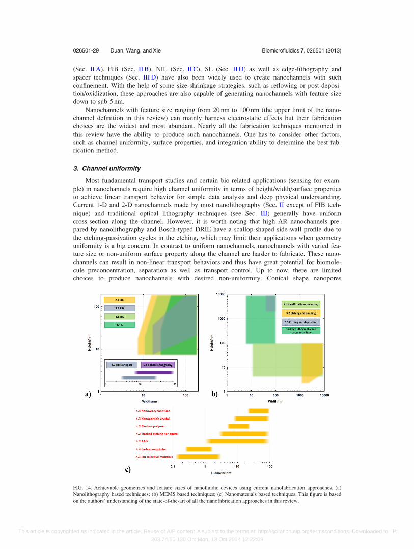
(Sec. II A), FIB (Sec. II B), NIL (Sec. II C), SL (Sec. II D) as well as edge-lithography and
spacer techniques (Sec. III D) have also been widely used to create nanochannels with such
confinement. With the help of some size-shrinkage strategies, such as reflowing or post-deposi-
tion/oxidization, these approaches are also capable of generating nanochannels with feature size
down to sub-5 nm.
Nanochannels with feature size ranging from 20 nm to 100 nm (the upper limit of the nano-
channel definition in this review) can mainly harness electrostatic effects but their fabrication
choices are the widest and most abundant. Nearly all the fabrication techniques mentioned in
this review have the ability to produce such nanochannels. One has to consider other factors,
such as channel uniformity, surface properties, and integration ability to determine the best fab-
rication method.
3. Channel uniformity
Most fundamental transport studies and certain bio-related applications (sensing for exam-
ple) in nanochannels require high channel uniformity in terms of height/width/surface properties
to achieve linear transport behavior for simple data analysis and deep physical understanding.
Current 1-D and 2-D nanochannels made by most nanolithography (Sec. II except of FIB tech-
nique) and traditional optical lithography techniques (see Sec. III) generally have uniform
cross-section along the channel. However, it is worth noting that high AR nanochannels pre-
pared by nanolithography and Bosch-typed DRIE have a scallop-shaped side-wall profile due to
the etching-passivation cycles in the etching, which may limit their applications when geometry
uniformity is a big concern. In contrast to uniform nanochannels, nanochannels with varied fea-
ture size or non-uniform surface property along the channel are harder to fabricate. These nano-
channels can result in non-linear transport behaviors and thus have great potential for biomole-
cule preconcentration, separation as well as transport control. Up to now, there are limited
choices to produce nanochannels with desired non-uniformity. Conical shape nanopores
FIG. 14. Achievable geometries and feature sizes of nanofluidic devices using current nanofabrication approaches. (a)
Nanolithography based techniques; (b) MEMS based techniques; (c) Nanomaterials based techniques. This figure is based
on the authors’ understanding of the state-of-the-art of all the nanofabrication approaches in this review.
026501-29 Duan, Wang, and Xie Biomicrofluidics 7, 026501 (2013)
This article is copyrighted as indicated in the article. Reuse of AIP content is subject to the terms at: http://scitation.aip.org/termsconditions. Downloaded to IP:
203.24.50.130 On: Mon, 13 Oct 2014 12:22:09

prepared by FIB (Sec. II B) and track etching (Sec. IV B) are probably the simplest nonlinear
nanofluidic devices. Besides nanopores, 1-D/2-D nanochannels with non-uniform channel height
can be made by slightly modifying a fabrication scheme of uniform nanochannels. For example,
tapered nanochannels can be made during a sacrificial layer releasing process if an etchant with
low selectivity is chosen.4 Recently, a so-called nanoglassblowing technique was developed to
fabricate integrated microfluidic and nanofluidic device with gradual depth variation and wide,
shallow nanochannels.314 In addition to these methods for fabricating channels with non-
uniform geometry, it is worth mentioning that nanochannel with non-uniform surface properties
can be formed by a diffusion-limited patterning (DLP) technique,5 which provides an alterna-
tive solution of introducing non-linear transport behaviors.
C. Other considerations
Besides materials and geometry concerns, one also has to consider other factors, such as
integration ability and observation, to determine the best fabrication strategy for a target nano-
fluidic device.
Nanochannels that are capable of integrating with other fluidic/electronic components are
highly desired for micro total analysis systems. As listed in Tables I–III, currently, 1-D or 2-D
nanochannels formed by various bulk/surface etching techniques (Secs. II and III, no matter
which type of lithography technique is involved) have good integration ability since other func-
tional components can be fabricated on the same substrate. Or, with the help of wafer-level
alignment and bonding operations, nanochannel can be integrated with microchannel and reser-
voirs on different substrates. Compared with these channels, 0-D nanochannels/nanopores and
other 1-D nanochannels based on nanomaterials are rather difficult for integration, which
restricts their practical applications to some extent.
For studies and applications that involve accurate optical measurements, transparent nano-
channels with thin capping layers are preferred since they can lower signal loss, increase image
contrast, and reduce the necessities of using long-working distance objective lens. Such nano-
channels can be fabricated by sacrificial layer releasing (Sec. III A), etching and deposition
(Sec. III C) as well as assembling of 1-D nanomaterials (Sec. IV D). Because the capping layer
formed by these techniques can be as thin as several hundred nanometers, these channels can
also be integrated with other advanced optical techniques (e.g., whispering gallery mode of op-
tical microcavity, surface enhanced Raman, etc.) for ultra-sensitive optical detection. It is worth
noting that among these three techniques, sacrificial layer releasing is the only one that has the
ability to fabricate 2-D shallow nanochannels with large optical observation window.
VII. FUTURE PROSPECTS
The past ten years have witnessed the booming development of nanofabrication techniques
for nanofluidic devices as summarized above. It is believed with much confidence that in the
next ten years, the nanofluidics related studies will remain popular and get fruitful achievements
from fundamental understanding of ion and molecule transport at the nanoscale to novel multi-
disciplinary applications in bio- and energy-related fields. The fast growth of nanofluidics keeps
calling for efforts to fabricate nanochannel/nanopore with smaller feature size, to design nano-
fluidic device with more flexibility in geometry, surface property and function, and in some
cases, to prototype the principle device in a more economical and simple way.
Capability of fabricating nanochannels with feature size smaller than 5 nm will definitely
take the present nanofluidics study to a whole new level.2,16,125,262 The confined space with
only several tens of layers of molecules existing presents an unprecedented opportunity to
explore anomalous fluids transport at the nanoscale, such as enhanced water transport in
SWCNT or cation mobility in 2-nm silica nanochannels,16,125 which may have a huge impact
to address ever-increasing energy demands and environment issues. On the other hand, further
development of such fabrication approaches will also expand nanofluidics applications in
bio-related fields as nanochannels with feature size less than 5 nm are perfect tools for single
molecule studies306,315 as well as direct manipulation of physiological media.125,309 The key
026501-30 Duan, Wang, and Xie Biomicrofluidics 7, 026501 (2013)
This article is copyrighted as indicated in the article. Reuse of AIP content is subject to the terms at: http://scitation.aip.org/termsconditions. Downloaded to IP:
203.24.50.130 On: Mon, 13 Oct 2014 12:22:09

challenge here is how to define the sub-5 nm feature in a reliable and pre-designable way. The
state-of-the-art of the laboratory fabrication, as summarized in Sec. VI B, has already demon-
strated its ability in preparing ultra-fine nanostructures. Moreover, combined fabrication strat-
egy, such as EBL plus ALD, could even provide possible solutions for nanofluidic device prep-
aration with feature size down to sub-5 nm. Besides developing new approaches based on
current mature techniques, one may also consider explore new fabrication method, especially
based on recent advanced facilities. For example, the helium ion microscope (HIM), which uses
a helium gas field ion source, is believed to be one of the most possible facilities for top-down
nanofabrication directly achieving a feature size smaller than 1 nm.316,317 HIM is capable of
imaging, milling or gas-assisted material deposition with an ultra-fine resolution due to its high
source brightness, low energy spread, and small diffraction effects. However, HIM is still in its
early stages of development and needs further improvements to fabricate applicable nanofluidic
devices for both fundamental studies and practical applications.
Nowadays, electrokinetics in some unconventional channels, like funnel or rhombus shaped,
with feature size varied from nanometer to micrometer, are attracting broad attentions in nano-
fluidics because of many non-linear ion transport behaviors in these asymmetric struc-
tures.6,17,142,220,225,228,315,318 However, the continuously varied feature size presents a serious
fabrication challenge as either expensive mask/exposure system or lengthy process time is
required for traditional lithography and direct-writing nanolithography, respectively. So far, the
available solutions are the etching-and-deposition approach318 and sacrificial layer releasing
approach,4 although their size controllability and integration reliability are far from the require-
ment and still need further improvements. Besides the challenge of achieving gradual-changing
geometry, nanofluidics researchers also face difficulties in realizing heterogeneous nanofluidic
devices with tunable surface properties. Several techniques including DLP,5 sequentially pattern-
ing different oxides,299 and packing different nanoparticles249,250 have been invented to form
nanofluidics diodes with opposite surface charge polarities. However, simpler and more scalable
methods are still desired to further explore the fundamental of heterogeneous nanofluidics and
expand its application as well. More importantly, further efforts are required to integrate nano-
fabrication process with traditional microfabrication techniques to realize the fluidic and electri-
cal connections between the key nanoscale component and the supportive macroscopic world.
Although many nanofabrication approaches reviewed in the paper are compatible with microfab-
rication (see discussion in Sec. VI C), some issues still exist in the present integration process,
such as collapses in bonding, un-expected residues in sacrificial layer releasing or photoresist re-
moval, and thus continuously call for efforts to improve the process reliability and yield.
Last but not the least, facile nanofabrication techniques with low cost, fast processes, and
simple facility requirements, like soft-lithography in microfluidics, are still in high demand,
especially for rapid prototyping of novel nanofluidics principles.18,19,21,24 Cutting down the fab-
rication cost will be helpful to expand nanofluidic study to much broader research. However,
present nanofabrication techniques that fulfilled the above requirements are usually suffering
from poor size controllability and limited process integratability. A material that cherishes the
same easy fabrication ability of PDMS but with a relatively larger Young’s modulus, which
means less collapse risk, might enable a soft-lithography typed nanofabrication approach for
nanofluidic devices, such as the recent effort of using hard PDMS in nanofluidic device prepa-
ration.25 Using nanomaterials, like nanotubes or nanoparticles, on the other hand, might provide
a promising choice for nanofabrication approaches that satisfy the required criteria, if they can
be formed to an organized nanocomponent in a predefined micro/macro structure by self-
assembly or in situ synthesis. Recently, mesoporous silica film319–321 that was prepared by
directional synthesis might be a good candidate for facile nanofabrication based on nanomate-
rial strategy as it can be easy to manipulate and integrate with current PDMS-based microflui-
dic devices. The development of material science will keep providing more and more choices
for facile nanofabrication. Researchers with interests in nanofluidics may pay close attention to
related advancements.
Overall, with the advancement of nanofabrication techniques, it is foreseeable that more
and more nanofluidic devices with high precise size controllability, unique geometrical
026501-31 Duan, Wang, and Xie Biomicrofluidics 7, 026501 (2013)
This article is copyrighted as indicated in the article. Reuse of AIP content is subject to the terms at: http://scitation.aip.org/termsconditions. Downloaded to IP:
203.24.50.130 On: Mon, 13 Oct 2014 12:22:09

structures, controllable surface properties and more integrated powerful functions will be
reported in the near future to further explore nanofluidics.
ACKNOWLEDGMENTS
C.D. is grateful to Boston University for providing start-up funding for his lab. W.W. would
like to thank the Major State Basic Research Development Program (973 Program) (Grant Nos.
2009CB320300 and 2011CB309502), the National Natural Science Foundation of China (Grant
Nos. 60976086 and 91023045), and the 985-III program (clinical applications) in Peking University
for their financial support.
1J. C. T. Eijkel and A. v. d. Berg, “Nanofluidics: What is it and what can we expect from it?” Microfluid. Nanofluid. 1(3),249–267 (2005).
2W. Sparreboom, A. van den Berg, and J. C. Eijkel, “Principles and applications of nanofluidic transport,” Nat.Nanotechnol. 4(11), 713–720 (2009).
3N. R. Tas, P. Mela, T. Kramer, J. W. Berenschot, and A. van den Berg, “Capillarity induced negative pressure of waterplugs in nanochannels,” Nano Lett. 3(11), 1537–1540 (2003).
4C. Duan, R. Karnik, M. C. Lu, and A. Majumdar, “Evaporation-induced cavitation in nanofluidic channels,” Proc. Natl.Acad. Sci. U.S.A. 109(10), 3683–3693 (2012).
5R. Karnik, K. Castelino, C. H. Duan, and A. Majumdar, “Diffusion-limited patterning of molecules in nanofluidicchannels,” Nano Lett. 6(8), 1735–1740 (2006).
6H. C. Chang and G. Yossifon, “Understanding electrokinetics at the nanoscale: A perspective,” Biomicrofluidics 3(1),012001 (2009).
7D. Stein, M. Kruithof, and C. Dekker, “Surface-charge-governed ion transport in nanofluidic channels,” Phys. Rev. Lett.93(3), 035901 (2004).
8J. O. Tegenfeldt, H. Cao, W. W. Reisner, C. Prinz, R. H. Austin, S. Y. Chou, E. C. Cox, and J. C. Sturm, “StretchingDNA in nanochannels,” Biophys. J. 86(1), 596A (2004).
9P. Abgrall and N. T. Nguyen, “Nanofluidic devices and their applications,” Anal. Chem. 80(7), 2326–2341 (2008).10R. Schoch, J. Han, and P. Renaud, “Transport phenomena in nanofluidics,” Rev. Mod. Phys. 80(3), 839–883 (2008).11D. Xia, J. Yan, and S. Hou, “Fabrication of nanofluidic biochips with nanochannels for applications in DNA analysis,”
Small 8(18), 2787–2801 (2012).12H. Daiguji, P. Yang, A. J. Szeri, and A. Majumdar, “Electrochemomechanical energy conversion in nanofluidic
channels,” Nano Lett. 4(12), 2315–2321 (2004).13D.-K. Kim, C. Duan, Y.-F. Chen, and A. Majumdar, “Power generation from concentration gradient by reverse electro-
dialysis in ion-selective nanochannels,” Microfluid. Nanofluid. 9(6), 1215–1224 (2010).14S. Moghaddam, E. Pengwang, Y. B. Jiang, A. R. Garcia, D. J. Burnett, C. J. Brinker, R. I. Masel, and M. A. Shannon,
“An inorganic-organic proton exchange membrane for fuel cells with a controlled nanoscale pore structure,” Nat.Nanotechnol. 5(3), 230–236 (2010).
15S. J. Kim, S. H. Ko, K. H. Kang, and J. Han, “Direct seawater desalination by ion concentration polarization,” Nat.Nanotechnol. 5(4), 297–301 (2010).
16J. K. Holt, H. G. Park, Y. M. Wang, M. Stadermann, A. B. Artyukhin, C. P. Grigoropoulos, A. Noy, and O. Bakajin,“Fast mass transport through sub-2-nanometer carbon nanotubes,” Science 312(5776), 1034–1037 (2006).
17M. R. Powell, M. Sullivan, I. Vlassiouk, D. Constantin, O. Sudre, C. C. Martens, R. S. Eisenberg, and Z. S. Siwy,“Nanoprecipitation-assisted ion current oscillations,” Nat. Nanotechnol. 3(1), 51–57 (2008).
18B. D. Gates, Q. Xu, J. C. Love, D. B. Wolfe, and G. M. Whitesides, “Unconventional nanofabrication,” Annu. Rev.Mater. Res. 34(1), 339–372 (2004).
19B. D. Gates, Q. Xu, M. Stewart, D. Ryan, C. G. Willson, and G. M. Whitesides, “New approaches to nanofabrication:Molding, printing, and other techniques,” Chem. Rev. 105(4), 1171–1196 (2005).
20J. L. Perry and S. G. Kandlikar, “Review of fabrication of nanochannels for single phase liquid flow,” Microfluid.Nanofluid. 2(3), 185–193 (2005).
21D. Mijatovic, J. C. Eijkel, and A. van den Berg, “Technologies for nanofluidic systems: Top-down vs. bottom-up–areview,” Lab Chip 5(5), 492–500 (2005).
22C. Dekker, “Solid-state nanopores,” Nat. Nanotechnol. 2(4), 209–215 (2007).23S. Prakash, A. Piruska, E. N. Gatimu, P. W. Bohn, J. V. Sweedler, and M. A. Shannon, “Nanofluidic: Systems and
applications,” IEEE Sens. J. 8(5), 441–450 (2008).24Y. Chen and A. Pepin, “Nanofabrication: Concentional and nonconventional methods,” Electrophoresis 22, 187–207
(2001).25J. M. Perry, K. Zhou, Z. D. Harms, and S. C. Jacobson, “Ion transport in nanofluidic funnels,” ACS Nano 4(7),
3897–3902 (2010).26S. H. Kim, Y. Cui, M. J. Lee, S. W. Nam, D. Oh, S. H. Kang, Y. S. Kim, and S. Park, “Simple fabrication of hydrophilic
nanochannels using the chemical bonding between activated ultrathin PDMS layer and cover glass by oxygen plasma,”Lab Chip 11(2), 348–353 (2011).
27R. Yokokawa, Y. Yoshida, S. Takeuchi, T. Kon, and H. Fujita, “Unidirectional transport of a bead on a single microtu-bule immobilized in a submicrometre channel,” Nanotechnology 17(1), 289–294 (2006).
28A. Hibara, T. Saito, H. B. Kim, M. Tokeshi, T. Ooi, M. Nakao, and T. Kitamori, “Nanochannels on a fused-silica micro-chip and liquid properties investigation by time-resolved fluorescence measurements,” Anal. Chem. 74(24), 6170–6176(2002).
29T. Tsukahara, W. Mizutani, K. Mawatari, and T. Kitamori, “NMR studies of structure and dynamics of liquid moleculesconfined in extended nanospaces,” J. Phys. Chem. B 113(31), 10808–10816 (2009).
026501-32 Duan, Wang, and Xie Biomicrofluidics 7, 026501 (2013)
This article is copyrighted as indicated in the article. Reuse of AIP content is subject to the terms at: http://scitation.aip.org/termsconditions. Downloaded to IP:
203.24.50.130 On: Mon, 13 Oct 2014 12:22:09

30E. Tamaki, A. Hibara, H. B. Kim, M. Tokeshi, and T. Kitamori, “Pressure-driven flow control system for nanofluidicchemical process,” J. Chromatogr. A 1137(2), 256–262 (2006).
31Z. D. Harms, K. B. Mogensen, P. S. Nunes, K. Zhou, B. W. Hildenbrand, I. Mitra, Z. Tan, A. Zlotnick, J. P. Kutter, andS. C. Jacobson, “Nanofluidic devices with two pores in series for resistive-pulse sensing of single virus capsids,” Anal.Chem. 83(24), 9573–9578 (2011).
32S. L. Levy, J. T. Mannion, J. Cheng, C. H. Reccius, and H. G. Craighead, “Entropic unfolding of DNA molecules innanofluidic channels,” Nano Lett. 8(11), 3839–3844 (2008).
33R. Riehn, R. H. Austin, and J. C. Sturm, “A nanofluidic railroad switch for DNA,” Nano Lett. 6(9), 1973–1976 (2006).34W. Reisner, J. Beech, N. Larsen, H. Flyvbjerg, A. Kristensen, and J. Tegenfeldt, “Nanoconfinement-enhanced conforma-
tional response of single DNA molecules to changes in ionic environment,” Phys. Rev. Lett. 99(5), 058302 (2007).35S. W. Nam, M. H. Lee, S. H. Lee, D. J. Lee, S. M. Rossnagel, and K. B. Kim, “Sub-10-nm nanochannels by self-sealing
and self-limiting atomic layer deposition,” Nano Lett. 10(9), 3324–3329 (2010).36M. Fouad, M. Yavuz, and B. Cui, “Nanofluidic channels fabricated by e-beam lithography and polymer reflow sealing,”
J. Vac. Sci. Technol. B 28(6), C6I11–C6I13 (2010).37C. K. Tung, R. Riehn, and R. H. Austin, “Complementary metal oxide semiconductor compatible fabrication and charac-
terization of parylene-C covered nanofluidic channels with integrated nanoelectrodes,” Biomicrofluidics 3(3), 031101(2009).
38A. A. Tseng, “Recent developments in nanofabrication using focused ion beams,” Small 1(10), 924–939 (2005).39A. A. Tseng, “Recent developments in micromilling using focused ion beam technology,” J. Micromech. Microeng.
14(4), R15–R34 (2004).40P. Chen, J. J. Gu, E. Brandin, Y. R. Kim, Q. Wang, and D. Branton, “Probing single DNA molecule transport using fab-
ricated nanopores,” Nano Lett. 4(11), 2293–2298 (2004).41C. Danelon, C. Santschi, J. Brugger, and H. Vogel, “Fabrication and functionalization of nanochannels by electron-
beam-induced silicon oxide deposition,” Langmuir 22(25), 10711–10715 (2006).42V. Mussi, P. Fanzio, L. Repetto, G. Firpo, P. Scaruffi, S. Stigliani, G. P. Tonini, and U. Valbusa, “DNA-functionalized
solid state nanopore for biosensing,” Nanotechnology 21(14), 145102 (2010).43H. D. Tong, H. V. Jansen, V. J. Gadgil, C. G. Bostan, E. Berenschot, C. J. M. van Rijn, and M. Elwenspoek, “Silicon
nitride nanosieve membrane,” Nano Lett. 4(2), 283–287 (2004).44Z. P. Tian, K. Lu, and B. Chen, “Unique nanopore pattern formation by focused ion beam guided anodization,”
Nanotechnology 21(40), 405301 (2010).45D. M. Cannon, B. R. Flachsbart, M. A. Shannon, J. V. Sweedler, and P. W. Bohn, “Fabrication of single nanofluidic
channels in poly(methylmethacrylate) films via focused-ion beam milling for use as molecular gates,” Appl. Phys. Lett.85(7), 1241–1243 (2004).
46A. A. Tseng, I. A. Insua, J. S. Park, B. Li, G. P. Vakanas, “Milling of submicron channels on gold layer using doublecharged arsenic ion beam,” J. Vac. Sci. Technol. B 22(1), 82–89 (2004).
47L. Guan, K. Peng, Y. Yang, X. Qiu, and C. Wang, “The nanofabrication of polydimethylsiloxane using a focused ionbeam,” Nanotechnology 20(14), 145301 (2009).
48L. Frey, C. Lehrer, and H. Ryssel, “Nanoscale effects in focused ion beam processing,” Appl. Phys. A: Mater. Sci.Process. 76(7), 1017–1023 (2003).
49H.-W. Li, D.-J. Kang, M. G. Blamire, and W. T. Huck, “Focused ion beam fabrication of silicon print masters,”Nanotechnology 14, 220–223 (2003).
50T. Yamamoto and T. Fujii, “Nanofluidic single-molecule sorting of DNA: A new concept in separation and analysis ofbiomolecules towards ultimate level performance,” Nanotechnology 21(39), 395502 (2010).
51L. D. Menard and J. M. Ramsey, “Fabrication of sub-5 nm nanochannels in insulating substrates using focused ion beammilling,” Nano Lett. 11(2), 512–517 (2011).
52T. Maleki, S. Mohammadi, and B. Ziaie, “A nanofluidic channel with embedded transverse nanoelectrodes,”Nanotechnology 20(10), 105302 (2009).
53A. A. Tseng, I. A. Insua, J.-S. Park, and C. D. Chen, “Milling yield estimation in focused ion beam milling of two-layersubstrates,” J. Micromech. Microeng. 15(1), 20–28 (2005).
54E. Angeli, C. Manneschi, L. Repetto, G. Firpo, and U. Valbusa, “DNA manipulation with elastomeric nanostructuresfabricated by soft-moulding of a FIB-patterned stamp,” Lab Chip 11(15), 2625–2629 (2011).
55P. Fanzio, V. Mussi, C. Manneschi, E. Angeli, G. Firpo, L. Repetto, and U. Valbusa, “DNA detection with a polymericnanochannel device,” Lab Chip 11(17), 2961–2966 (2011).
56J. Wu, R. Chantiwas, A. Amirsadeghi, S. A. Soper, and S. Park, “Complete plastic nanofluidic devices for DNA analysisvia direct imprinting with polymer stamps,” Lab Chip 11(17), 2984–2989 (2011).
57L. J. Guo, “Nanoimprint lithography: Methods and material requirements,” Adv. Mater. 19(4), 495–513 (2007).58X. Li, X. Wang, J. Jin, Q. Tang, Y. Tian, S. Fu, and Z. Cui, “Fabrication of micro/nano fluidic system combining hybrid
mask-mould lithography with thermal bonding,” Microelectron. Eng. 87(5–8), 722–725 (2010).59B. Yang, V. R. Dukkipati, D. Li, B. L. Cardozo, S. W. Pang, “Stretching and selective immobilization of DNA in SU-8
micro- and nanochannels,” J. Vac. Sci. Technol. B 25(6), 2352–2356 (2007).60L. H. Thamdrup, A. Klukowska, and A. Kristensen, “Stretching DNA in polymer nanochannels fabricated by thermal
imprint in PMMA,” Nanotechnology 19(12), 125301 (2008).61Y. H. Cho, J. Park, H. Park, X. Cheng, B. J. Kim, and A. Han, “Fabrication of high-aspect-ratio polymer nanochannels
using a novel Si nanoimprint mold and solvent-assisted sealing,” Microfluid. Nanofluid. 9(2–3), 163–170 (2009).62Q. Xia, K. J. Morton, R. H. Austin, and S. Y. Chou, “Sub-10 nm self-enclosed self-limited nanofluidic channel arrays,”
Nano Lett. 8(11), 3830–3833 (2008).63L. J. Guo, X. Cheng, and C. F. Chou, “Fabrication of size-controllable nanofluidic channels by nanoimprinting and its
application for DNA stretching,” Nano Lett. 4(1), 69–73 (2004).64R. Chantiwas, M. L. Hupert, S. R. Pullagurla, S. Balamurugan, J. Tamarit-Lopez, S. Park, P. Datta, J. Goettert, Y. K.
Cho, and S. A. Soper, “Simple replication methods for producing nanoslits in thermoplastics and the transport dynamicsof double-stranded DNA through these slits,” Lab Chip 10(23), 3255–3264 (2010).
026501-33 Duan, Wang, and Xie Biomicrofluidics 7, 026501 (2013)
This article is copyrighted as indicated in the article. Reuse of AIP content is subject to the terms at: http://scitation.aip.org/termsconditions. Downloaded to IP:
203.24.50.130 On: Mon, 13 Oct 2014 12:22:09

65M. B. Mikkelsen, A. A. Letailleur, E. Sondergard, E. Barthel, J. Teisseire, R. Marie, and A. Kristensen, “All-silica nano-fluidic devices for DNA-analysis fabricated by imprint of sol-gel silica with silicon stamp,” Lab Chip 12(2), 262–267(2012).
66N. R. Hendricks, J. J. Watkins, and K. R. Carter, “Formation of hierarchical silica nanochannels through nanoimprintlithography.” J. Mater. Chem. 21(37), 14213–14218 (2011).
67R. M. Reano and S. W. Pang, “Sealed three-dimensional nanochannels,” J. Vac. Sci. Technol. B 23(6), 2995–2999(2005).
68X. Liang and S. Y. Chou, “Nanogap detector inside nanofluidic channel for fast real-time label-free DNA analysis,”Nano Lett. 8(5), 1472–1476 (2008).
69D. Xia, Z. Ku, S. C. Lee, and S. R. Brueck, “Nanostructures and functional materials fabricated by interferometric lith-ography,” Adv. Mater. 23(2), 147–179 (2011).
70Y. J. Oh, T. C. Gamble, D. Leonhardt, C. H. Chung, S. R. Brueck, C. F. Ivory, G. P. Lopez, D. N. Petsev, and S. M.Han, “Monitoring FET flow control and wall adsorption of charged fluorescent dye molecules in nanochannels integratedinto a multiple internal reflection infrared waveguide,” Lab Chip 8(2), 251–258 (2008).
71Y. J. Oh, D. Bottenus, C. F. Ivory, and S. M. Han, “Impact of leakage current and electrolysis on FET flow control andpH changes in nanofluidic channels,” Lab Chip 9(11), 1609–1617 (2009).
72M. J. O’Brien, P. Bisong, L. K. Ista, E. M. Rabinovich, A. L. Garcia, S. S. Sibbett, G. P. Lopez, and S. R. J. Brueck,“Fabrication of an integrated nanofluidic chip using interferometric lithography,” J. Vac. Sci. Technol. B 21(6),2941–2945 (2003).
73D. Bottenus, Y. J. Oh, S. M. Han, and C. F. Ivory, “Experimentally and theoretically observed native pH shifts in a nano-channel array,” Lab Chip 9(2), 219–231 (2009).
74A. L. Garcia, L. K. Ista, D. N. Petsev, M. J. O’Brien, P. Bisong, A. A. Mammoli, S. R. Brueck, and G. P. Lopez,“Electrokinetic molecular separation in nanoscale fluidic channels,” Lab Chip 5(11), 1271–1276 (2005).
75Y. J. Oh, A. L. Garcia, D. N. Petsev, G. P. Lopez, S. R. Brueck, C. F. Ivory, and S. M. Han, “Effect of wall-moleculeinteractions on electrokinetic transport of charged molecules in nanofluidic channels during FET flow control,” LabChip 9(11), 1601–1608 (2009).
76Y. Zhang, T. C. Gamble, A. Neumann, G. P. Lopez, S. R. Brueck, and D. N. Petsev, “Electric field control and analytetransport in Si/SiO2 fluidic nanochannels,” Lab Chip 8(10), 1671–1675 (2008).
77Y. Kim, K. S. Kim, K. L. Kounovsky, R. Chang, G. Y. Jung, J. J. dePablo, K. Jo, and D. C. Schwartz, “Nanochannelconfinement: DNA stretch approaching full contour length,” Lab Chip 11(10), 1721–1729 (2011).
78N. M. Elman, K. Daniel, F. Jalali-Yazdi, and M. J. Cima, “Super permeable nano-channel membranes defined with laserinterferometric lithography,” Microfluid. Nanofluid. 8(4), 557–563 (2009).
79H. M. Chen, L. Pang, M. S. Gordon, and Y. Fainman, “Real-time template-assisted manipulation of nanoparticles in amultilayer nanofluidic chip,” Small 7(19), 2750–2757 (2011).
80G. Zhang and D. Wang, “Colloidal lithography–The art of nanochemical patterning,” Chem. Asian J. 4(2), 236–245(2009).
81Y. Li, W. Cai, and G. Duan, “Ordered micro/nanostructured arrays based on the monolayer colloidal crystals,” Chem.Mater. 20(3), 615–624 (2008).
82N. Vogel, C. K. Weiss, and K. Landfester, “From soft to hard: The generation of functional and complex colloidal mono-layers for nanolithography,” Soft Matter 8(15), 4044 (2012).
83A. V. Whitney, B. D. Myers, and R. P. Van Duyne, “Sub-100 nm triangular nanopores fabricated with the reactive ionetching variant of nanosphere lithography and angle-resolved nanosphere lithography,” Nano Lett. 4(8), 1507–1511(2004).
84N. Denkov, O. Velev, P. Kralchevski, I. Ivanov, H. Yoshimura, and K. Nagayama, “Mechanism of formation of two-dimensional crystals from latex particles on substrates,” Langmuir 8(12), 3183–3190 (1992).
85J. Huang, F. Kim, A. R. Tao, S. Connor, and P. Yang, “Spontaneous formation of nanoparticle stripe patterns throughdewetting,” Nature Mater. 4(12), 896–900 (2005).
86C.-M. Hsu, S. T. Connor, M. X. Tang, and Y. Cui, “Wafer-scale silicon nanopillars and nanocones byLangmuir–Blodgett assembly and etching,” Appl. Phys. Lett. 93(13), 133109 (2008).
87S. Jeong, L. Hu, H. R. Lee, E. Garnett, J. W. Choi, and Y. Cui, “Fast and scalable printing of large area monolayer nano-particles for nanotexturing applications,” Nano Lett. 10(8), 2989–2994 (2010).
88Z. X. Lu, A. Namboodiri, and M. M. Collinson, “Self-supporting nanopore membranes with controlled pore size andshape,” ACS Nano 2(5), 993–999 (2008).
89M. B. Stern, M. W. Geis, and J. E. Curtin, “Nanochannel fabrication for chemical sensors,” J. Vac. Sci. Technol. B15(6), 2887–2891 (1997).
90R. Karnik, R. Fan, M. Yue, D. Li, P. Yang, and A. Majumdar, “Electrostatic control of ions and molecules in nanofluidictransistors,” Nano Lett. 5(5), 943–948 (2005).
91R. Karnik, K. Castelino, R. Fan, P. Yang, and A. Majumdar, “Effects of biological reactions and modifications on con-ductance of nanofluidic channels,” Nano Lett. 5(9), 1638–1642 (2005).
92R. Karnik, K. Castelino, and A. Majumdar, “Field-effect control of protein transport in a nanofluidic transistor circuit,”Appl. Phys. Lett. 88(12), 123114 (2006).
93R. Karnik, C. Duan, K. Castelino, H. Daiguji, and A. Majumdar, “Rectification of ionic current in a nanofluidic diode,”Nano Lett. 7(3), 547–551 (2007).
94L. J. Cheng and L. J. Guo, “Rectified ion transport through concentration gradient in homogeneous silica nanochannels,”Nano Lett. 7(10), 3165–3171 (2007).
95R. A. Barton, B. Ilic, S. S. Verbridge, B. R. Cipriany, J. M. Parpia, and H. G. Craighead, “Fabrication of a nanomechani-cal mass sensor containing a nanofluidic channel,” Nano Lett. 10(6), 2058–2063 (2010).
96T. S. Hug, N. F. de Rooij, and U. Staufer, “Fabrication and electroosmotic flow measurements in micro- and nanofluidicchannels,” Microfluid. Nanofluid. 2(2), 117–124 (2006).
97C. Shen, V. R. S. S. Mokkapati, H. T. M. Pham, and P. M. Sarro, “Micromachined nanofiltration modules for lab-on-a-chip applications,” J. Micromech. Microeng. 22(2), 025003 (2012).
026501-34 Duan, Wang, and Xie Biomicrofluidics 7, 026501 (2013)
This article is copyrighted as indicated in the article. Reuse of AIP content is subject to the terms at: http://scitation.aip.org/termsconditions. Downloaded to IP:
203.24.50.130 On: Mon, 13 Oct 2014 12:22:09

98J. C. Eijkel, J. Bomer, N. R. Tas, and A. van den Berg, “1-D nanochannels fabricated in polyimide,” Lab Chip 4(3),161–163 (2004).
99M. N. Hamblin, A. R. Hawkins, D. Murray, D. Maynes, M. L. Lee, A. T. Woolley, and H. D. Tolley, “Capillary flow insacrificially etched nanochannels,” Biomicrofluidics 5(2), 021103 (2011).
100K. P. Nichols, J. C. Eijkel, and H. J. Gardeniers, “Nanochannels in SU-8 with floor and ceiling metal electrodes and inte-grated microchannels,” Lab Chip 8(1), 173–175 (2008).
101M. A. Zevenbergen, P. S. Singh, E. D. Goluch, B. L. Wolfrum, and S. G. Lemay, “Stochastic sensing of single moleculesin a nanofluidic electrochemical device,” Nano Lett. 11(7), 2881–2886 (2011).
102M. N. Hamblin, J. Xuan, D. Maynes, H. D. Tolley, D. M. Belnap, A. T. Woolley, M. L. Lee, and A. R. Hawkins,“Selective trapping and concentration of nanoparticles and viruses in dual-height nanofluidic channels,” Lab Chip 10(2),173–178 (2010).
103W. Sparreboom, J. C. Eijkel, J. Bomer, and A. van den Berg, “Rapid sacrificial layer etching for the fabrication of nano-channels with integrated metal electrodes,” Lab Chip 8(3), 402–407 (2008).
104R. Sordan, A. Miranda, F. Traversi, D. Colombo, D. Chrastina, G. Isella, M. Masserini, L. Miglio, K. Kern, and K.Balasubramanian, “Vertical arrays of nanofluidic channels fabricated without nanolithography,” Lab Chip 9(11),1556–1560 (2009).
105H. Zeng, Z. Wan, and A. D. Feinerman, “Fabrication of micro/nano fluidic channels with sacrificial galvanic coupledmetals,” Nanotechnology 17(13), 3183–3188 (2006).
106C. Peng and S. W. Pang, “Three-dimensional nanochannels formed by fast etching of polymer,” J. Vac. Sci. Technol. B24(4), 1941–1946 (2006).
107S. Wang, X. Hu, and L. J. Lee, “Electrokinetics induced asymmetric transport in polymeric nanonozzles,” Lab Chip8(4), 573–581 (2008).
108L. M. Bellan, E. A. Strychalski, and H. G. Craighead, “Nanochannels fabricated in polydimethylsiloxane using sacrifi-cial electrospun polyethylene oxide nanofibers,” J. Vac. Sci. Technol. B 26(5), 1728–1731 (2008).
109S. Lee, K. Limkrailassiri, Y. Gao, C. Chang, and L. W. Lin, “Chip-to-chip fluidic connectors via near-field electro-spinning,” in Proceedings of IEEE MicroElectroMechanical Systems (IEEE, 2007), pp. 252–255.
110J. Guan, P. E. Boukany, O. Hemminger, N. R. Chiou, W. Zha, M. Cavanaugh, and L. J. Lee, “Large laterally orderednanochannel arrays from DNA combing and imprinting,” Adv. Mater. 22(36), 3997–4001 (2010).
111P. E. Boukany, A. Morss, W. C. Liao, B. Henslee, H. Jung, X. Zhang, B. Yu, X. Wang, Y. Wu, L. Li, K. Gao, X. Hu, X.Zhao, O. Hemminger, W. Lu, G. P. Lafyatis, and L. J. Lee, “Nanochannel electroporation delivers precise amounts ofbiomolecules into living cells,” Nat. Nanotechnol. 6(11), 747–754 (2011).
112N. R. Devlin and D. K. Brown, “Fabricating millimeter to nanometer sized cavities concurrently for nanofluidicdevices,” J. Vac. Sci. Technol. B 28(6), C6I7–C6I10 (2010).
113N. R. Devlin, D. K. Brown, and P. A. Kohl, “Patterning decomposable polynorbornene with electron beam lithographyto create nanochannels,” J. Vac. Sci. Technol. B 27(6), 2508–2511 (2009).
114C. K. Harnett, G. W. Coates, and H. G. Craighead, “Heat-depolymerizable polycarbonates as electron beam patternablesacrificial layers for nanofluidics,” J. Vac. Sci. Technol. B 19(6), 2842–2845 (2001).
115X. T. Huang, C. Gupta, and S. Pennathur, “A novel fabrication method for centimeter-long surface-micromachinednanochannels,” J. Micromech. Microeng. 20(1), 015040 (2010).
116H. T. Hoang, H. D. Tong, I. M. Segers-Nolten, N. R. Tas, V. Subramaniam, and M. C. Elwenspoek, “Wafer-scale thinencapsulated two-dimensional nanochannels and its application toward visualization of single molecules,” J. ColloidInterface Sci. 367(1), 455–459 (2012).
117A. Grattoni, D. Fine, E. Zabre, A. Ziemys, J. Gill, Y. Mackeyev, M. A. Cheney, D. C. Danila, S. Hosali, L. J. Wilson, F.Hussain, and M. Ferrari, “Gated and near-surface diffusion of charged fullerenes in nanochannels,” ACS Nano 5(12),9382–9391 (2011).
118H. T. Hoang, I. M. Segers-Nolten, J. W. Berenschot, M. J. de Boer, N. R. Tas, J. Haneveld, and M. C. Elwenspoek,“Fabrication and interfacing of nanochannel devices for single-molecule studies,” J. Micromech. Microeng. 19(6),065017 (2009).
119J. Haneveld, H. Jansen, E. Berenschot, N. Tas, and M. Elwenspoek, “Wet anisotropic etching for fluidic 1D nano-channels,” J. Micromech. Microeng. 13(4), S62–S66 (2003).
120M. Wang, N. Jing, I. H. Chou, G. L. Cote, and J. Kameoka, “An optofluidic device for surface enhanced Ramanspectroscopy,” Lab Chip 7(5), 630–632 (2007).
121Y. C. Wang and J. Han, “Pre-binding dynamic range and sensitivity enhancement for immuno-sensors using nanofluidicpreconcentrator,” Lab Chip 8(3), 392–394 (2008).
122R. B. Veenhuis, E. J. van der Wouden, J. W. van Nieuwkasteele, A. van den Berg, and J. C. Eijkel, “Field-effect basedattomole titrations in nanoconfinement,” Lab Chip 9(24), 3472–3480 (2009).
123D. Kim, A. Raj, L. Zhu, R. I. Masel, and M. A. Shannon, “Non-equilibrium electrokinetic micro/nano fluidic mixer,”Lab Chip 8(4), 625–628 (2008).
124S. J. Lee and D. Kim, “Millisecond-order rapid micromixing with non-equilibrium electrokinetic phenomena,”Microfluid. Nanofluid. 12, 897–906 (2011).
125C. Duan and A. Majumdar, “Anomalous ion transport in 2-nm hydrophilic nanochannels,” Nat. Nanotechnol. 5(12),848–852 (2010).
126P. Abgrall, L. N. Low, and N. T. Nguyen, “Fabrication of planar nanofluidic channels in a thermoplastic by hot-embossing and thermal bonding,” Lab Chip 7(4), 520–522 (2007).
127K.-D. Huang and R.-J. Yang, “Formation of ionic depletion/enrichment zones in a hybrid micro-/nano-channel,”Microfluid. Nanofluid. 5(5), 631–638 (2008).
128Z. Xu, J.-K. Wen, C. Liu, J.-S. Liu, L.-Q. Du, and L.-D. Wang, “Research on forming and application of U-form glassmicro-nanofluidic chip with long nanochannels,” Microfluid. Nanofluid. 7(3), 423–429 (2009).
129L. Shui, A. Berg, and J. C. T. Eijkel, “Scalable attoliter monodisperse droplet formation using multiphase nano-micro-fluidics,” Microfluid. Nanofluid. 11(1), 87–92 (2011).
130Q. S. Pu, J. S. Yun, H. Temkin, and S. R. Liu, “Ion-enrichment and ion-depletion effect of nanochannel structures,”Nano Lett. 4(6), 1099–1103 (2004).
026501-35 Duan, Wang, and Xie Biomicrofluidics 7, 026501 (2013)
This article is copyrighted as indicated in the article. Reuse of AIP content is subject to the terms at: http://scitation.aip.org/termsconditions. Downloaded to IP:
203.24.50.130 On: Mon, 13 Oct 2014 12:22:09

131S. Liu, Q. Pu, L. Gao, C. Korzeniewski, and C. Matzke, “From nanochannel-induced proton conduction enhancement toa nanochannel-based fuel cell,” Nano Lett. 5(7), 1389–1393 (2005).
132R. B. Schoch, L. F. Cheow, and J. Han, “Electrical detection of fast reaction kinetics in nanochannels with an inducedflow,” Nano Lett. 7(12), 3895–3900 (2007).
133J. J. Jones, J. R. van der Maarel, and P. S. Doyle, “Effect of nanochannel geometry on DNA structure in the presence ofmacromolecular crowding agent,” Nano Lett. 11(11), 5047–5053 (2011).
134I. H. Chou, M. Benford, H. T. Beier, G. L. Cote, M. Wang, N. Jing, J. Kameoka, and T. A. Good, “Nanofluidic biosens-ing for beta-amyloid detection using surface enhanced Raman spectroscopy,” Nano Lett. 8(6), 1729–1735 (2008).
135D. Stein, Z. Deurvorst, F. H. van der Heyden, W. J. Koopmans, A. Gabel, and C. Dekker, “Electrokinetic concentrationof DNA polymers in nanofluidic channels,” Nano Lett. 10(3), 765–772 (2010).
136P. Mao and J. Han, “Fabrication and characterization of 20 nm planar nanofluidic channels by glass-glass and glass-silicon bonding,” Lab Chip 5(8), 837–844 (2005).
137K. Pappaert, J. Biesemans, D. Clicq, S. Vankrunkelsven, and G. Desmet, “Measurements of diffusion coefficients in 1-Dmicro- and nanochannels using shear-driven flows,” Lab Chip 5(10), 1104–1110 (2005).
138N. F. Y. Durand, A. Bertsch, M. Todorova, and P. Renaud, “Direct measurement of effective diffusion coefficients innanochannels using steady-state dispersion effects,” Appl. Phys. Lett. 91(20), 203106 (2007).
139N. F. Durand and P. Renaud, “Label-free determination of protein-surface interaction kinetics by ionic conductanceinside a nanochannel,” Lab Chip 9(2), 319–324 (2009).
140A. Plecis, R. B. Schoch, and P. Renaud, “Ionic transport phenomena in nanofluidics: Experimental and theoretical studyof the exclusion-enrichment effect on a chip,” Nano Lett. 5(6), 1147–1155 (2005).
141R. B. Schoch, A. Bertsch, and P. Renaud, “pH-controlled diffusion of proteins with different pI values across a nano-channel on a chip,” Nano Lett. 6(3), 543–547 (2006).
142G. Yossifon, Y.-C. Chang, and H.-C. Chang, “Rectification, gating voltage, and interchannel communication of nanoslotarrays due to asymmetric entrance space charge polarization,” Phys. Rev. Lett. 103(15), 154502 (2009).
143V. R. Mokkapati, V. Di Virgilio, C. Shen, J. Mollinger, J. Bastemeijer, and A. Bossche, “DNA tracking within a nano-channel: Device fabrication and experiments,” Lab Chip 11(16), 2711–2719 (2011).
144H. T. Hoang, I. M. Segers-Nolten, N. R. Tas, J. W. van Honschoten, V. Subramaniam, and M. C. Elwenspoek, “Analysisof single quantum-dot mobility inside 1D nanochannel devices,” Nanotechnology 22(27), 275201 (2011).
145K. M. van Delft, J. C. Eijkel, D. Mijatovic, T. S. Druzhinina, H. Rathgen, N. R. Tas, A. van den Berg, and F. Mugele,“Micromachined Fabry-Perot interferometer with embedded nanochannels for nanoscale fluid dynamics,” Nano Lett.7(2), 345–350 (2007).
146M. Krishnan, I. Monch, and P. Schwille, “Spontaneous stretching of DNA in a two-dimensional nanoslit,” Nano Lett.7(5), 1270–1275 (2007).
147F. Persson, L. H. Thamdrup, M. B. L. Mikkelsen, S. E. Jaarlgard, P. Skafte-Pedersen, H. Bruus, A. Kristensen, “Doublethermal oxidation scheme for the fabrication of SiO2 nanochannels,” Nanotechnology 18(24), 245301 (2007).
148A. Grattoni, E. De Rosa, S. Ferrati, Z. Wang, A. Gianesini, X. Liu, F. Hussain, R. Goodall, and M. Ferrari, “Analysis ofa nanochanneled membrane structure through convective gas flow,” J. Micromech. Microeng. 19(11), 115018 (2009).
149C. Wu, Z. Jin, H. Wang, H. Ma, and Y. Wang, “Design and fabrication of a nanofluidic channel by selective thermal oxi-dation and etching back of silicon dioxide made on a silicon substrate,” J. Micromech. Microeng. 17(12), 2393–2397(2007).
150D. Fine, A. Grattoni, S. Hosali, A. Ziemys, E. De Rosa, J. Gill, R. Medema, L. Hudson, M. Kojic, M. Milosevic, L.Brousseau Iii, R. Goodall, M. Ferrari, and X. Liu, “A robust nanofluidic membrane with tunable zero-order release forimplantable dose specific drug delivery,” Lab Chip 10(22), 3074–3083 (2010).
151D. Fine, A. Grattoni, E. Zabre, F. Hussein, M. Ferrari, and X. Liu, “A low-voltage electrokinetic nanochannel drug deliv-ery system,” Lab Chip 11(15), 2526–2534 (2011).
152P. M. Sinha, G. Valco, S. Sharma, X. Liu, and M. Ferrari, “Nanoengineered device for drug delivery application,”Nanotechnology 15(10), S585–S589 (2004).
153C. R. Song and P. S. Wang, “Fabrication of sub-10 nm planar nanofluidic channels through native oxide etch and anodicwafer bonding,” IEEE Trans. Nanotechnol. 9(2), 138–141 (2010).
154W. P. Shih, C. Y. Hui, and N. C. Tien, “Collapse of microchannels during anodic bonding: Theory and experiments,”J. Appl. Phys. 95(5), 2800–2808 (2004).
155J. Haneveld, N. R. Tas, N. Brunets, H. V. Jansen, and M. Elwenspoek, “Capillary filling of sub-10 nm nanochannels,”J. Appl. Phys. 104(1), 014309 (2008).
156H. Y. Wang, R. S. Foote, S. C. Jacobson, J. H. Schneibel, and J. M. Ramsey, “Low temperature bonding for microfabri-cation of chemical analysis devices,” Sens. Actuators B 45(3), 199–207 (1997).
157T. P. Burg, M. Godin, S. M. Knudsen, W. Shen, G. Carlson, J. S. Foster, K. Babcock, and S. R. Manalis, “Weighing ofbiomolecules, single cells and single nanoparticles in fluid,” Nature 446(7139), 1066–1069 (2007).
158J. Lee, W. Shen, K. Payer, T. P. Burg, and S. R. Manalis, “Toward attogram mass measurements in solution with sus-pended nanochannel resonators,” Nano Lett. 10(7), 2537–2542 (2010).
159F. Devreux, P. Barboux, M. Filoche, and B. Sapoval, “A simplified model for glass dissolution in water,” J. Mater. Sci.36(6), 1331–1341 (2001).
160B. Ilic, D. Czaplewski, M. Zalalutdinov, B. Schmidt, and H. G. Craighead, “Fabrication of flexible polymer tubes formicro and nanofluidic applications,” J. Vac. Sci. Technol. B 20(6), 2459–2465 (2002).
161C. C. Wong, A. Agarwal, N. Balasubramanian, and D. L. Kwong, “Fabrication of self-sealed circular nano/microfluidicchannels in glass substrates,” Nanotechnology 18(13), 135304 (2007).
162L. Ji, J. K. Kim, Q. Ji, K. N. Leung, Y. Chen, and R. A. Gough, “Conformal metal thin-film coatings in high-aspect-ratiotrenches using a self-sputtered rf-driven plasma source,” J. Vac. Sci. Technol. B 25(4), 1227–1230 (2007).
163P. Mao and J. Han, “Massively-parallel ultra-high-aspect-ratio nanochannels as mesoporous membranes,” Lab Chip9(4), 586–591 (2009).
164J. C. Love, K. E. Paul, and G. M. Whitesides, “Fabrication of nanometer-scale features by controlled isotropic wet chem-ical etching,” Adv. Mater. 13(8), 604–607 (2001).
026501-36 Duan, Wang, and Xie Biomicrofluidics 7, 026501 (2013)
This article is copyrighted as indicated in the article. Reuse of AIP content is subject to the terms at: http://scitation.aip.org/termsconditions. Downloaded to IP:
203.24.50.130 On: Mon, 13 Oct 2014 12:22:09
165L. Q. Chen, M. B. Chan-Park, Y. H. Yan, Q. Zhang, C. M. Li, and J. Zhang, “High aspect ratio silicon nanomoulds forUV embossing fabricated by directional thermal oxidation using an oxidation mask,” Nanotechnology 18(35), 355307(2007).
166L. Q. Chen, M. B. Chan-Park, C. Yang, and Q. Zhang, “The residual pattern of double thin-film over-etching for the fab-rication of continuous patterns with dimensions varying from 50 nm to millimeters over a large area,” Nanotechnology19(15), 155301 (2008).
167Q. Xie, Q. Zhou, F. Xie, J. Sang, W. Wang, H. A. Zhang, W. Wu, and Z. Li, “Wafer-scale fabrication of high-aspect ra-tio nanochannels based on edge-lithography technique,” Biomicrofluidics 6(1), 016502 (2012).
168H. Y. Mao, W. G. Wu, Y. L. Zhang, G. Zhai, and J. Xu, “Fabrication of high-compact nanowires using alternating pho-toresist ashing and spacer technology,” J. Micromech. Microeng. 20(8), 085029 (2010).
169R. A. Smith, K. Goldman, W. H. Fissell, A. J. Fleischman, C. A. Zorman, and S. Roy, “Removal of endotoxin fromdeionized water using micromachined silicon nanopore membranes,” J. Micromech. Microeng. 21(5), 054029 (2011).
170C. Lee, E. H. Yang, N. V. Myung, and T. George, “A nanochannel fabrication technique without nanolithography,”Nano Lett. 3(10), 1339–1340 (2003).
171N. R. Tas, J. W. Berenschot, P. Mela, H. V. Jansen, M. Elwenspoek, and A. van den Berg, “2D-confined nanochannelsfabricated by conventional micromachining,” Nano Lett. 2(9), 1031–1032 (2002).
172K. Tybrandt, R. Forchheimer, and M. Berggren, “Logic gates based on ion transistors,” Nat. Commun. 3, 871 (2012).173E. O. Gabrielsson, K. Tybrandt, and M. Berggren, “Ion diode logics for pH control,” Lab Chip 12(14), 2507–2513
(2012).174H. Kim, J. Kim, E. G. Kim, A. J. Heinz, S. Kwon, and H. Chun, “Optofluidic in situ maskless lithography of charge
selective nanoporous hydrogel for DNA preconcentration,” Biomicrofluidics 4(4), 043014 (2010).175P. Kim, S. J. Kim, J. Han, and K. Y. Suh, “Stabilization of ion concentration polarization using a heterogeneous nanopo-
rous junction,” Nano Lett. 10(1), 16–23 (2010).176L. J. Cheng and H. C. Chang, “Microscale pH regulation by splitting water,” Biomicrofluidics 5(4), 046502 (2011).177Y. A. Song, R. Melik, A. N. Rabie, A. M. S. Ibrahim, D. Moses, A. Tan, J. Han, and S. J. Lin, “Electrochemical activa-
tion and inhibition of neuromuscular systems through modulation of ion concentrations with ion-selective membranes,”Nature Mater. 10, 980–986 (2011).
178X. Liu, C. Suo, Y. Zhang, X. Wang, C. Sun, L. Li, and L. Zhang, “Novel modification of NafionVR
117 for a MEMS-based micro direct methanol fuel cell (lDMFC),” J. Micromech. Microeng. 16(9), S226–S232 (2006).
179S. J. Kim and J. Han, “Self-sealed vertical polymeric nanoporous-junctions for high-throughput nanofluidicapplications,” Anal. Chem. 80(9), 3507–3511 (2008).
180J. H. Lee, Y. A. Song, and J. Han, “Multiplexed proteomic sample preconcentration device using surface-patterned ion-selective membrane,” Lab Chip 8(4), 596–601 (2008).
181R. Kwak, S. J. Kim, and J. Han, “Continuous-flow biomolecule and cell concentrator by ion concentration polarization,”Anal. Chem. 83(19), 7348–7355 (2011).
182J. H. Lee and J. Han, “Concentration-enhanced rapid detection of human chorionic gonadotropin (hCG) on a Au surfaceusing a nanofluidic preconcentrator,” Microfluid. Nanofluid. 9(4), 973–979 (2010).
183S. H. Ko, S. J. Kim, L. F. Cheow, L. D. Li, K. H. Kang, and J. Han, “Massively parallel concentration device for multi-plexed immunoassays,” Lab Chip 11(7), 1351–1358 (2011).
184A. Sarkar and J. Han, “Non-linear and linear enhancement of enzymatic reaction kinetics using a biomolecule concen-trator,” Lab Chip 11(15), 2569–2576 (2011).
185L. F. Cheow and J. Han, “Continuous signal enhancement for sensitive aptamer affinity probe electrophoresis assayusing electrokinetic concentration,” Anal. Chem. 83(18), 7086–7093 (2011).
186O. J€annig and N.-T. Nguyen, “A polymeric high-throughput pressure-driven micromixer using a nanoporous mem-brane,” Microfluid. Nanofluid. 10(3), 513–519 (2010).
187S. P. Adiga, C. Jin, L. A. Curtiss, N. A. Monteiro-Riviere, and R. J. Narayan, “Nanoporous membranes for medical andbiological applications,” Wiley Interdiscip. Rev. Nanomed. Nanobiotechnol. 1(5), 568–581 (2009).
188S. K. Vajandar, D. Xu, D. A. Markov, J. P. Wikswo, W. Hofmeister, and D. Li, “SiO2-coated porous anodic aluminamembranes for high flow rate electroosmotic pumping,” Nanotechnology 18(27), 275705 (2007).
189M. Ali, P. Ramirez, S. Mafe, R. Neumann, and W. Ensinger, “A pH-tunable nanofluidic diode with a broad range of rec-tifying properties,” ACS Nano 3(3), 603–608 (2009).
190H. Uehara, M. Kakiage, M. Sekiya, D. Sakuma, T. Yamonobe, N. Takano, A. Barraud, E. Meurville, and P. Ryser,“Size-selective diffusion in nanoporous but flexible membranes for glucose sensors,” ACS Nano 3(4), 924–932 (2009).
191F. Li, L. Zhang, and R. M. Metzger, “On the growth of highly ordered pores in anodized aluminum Oxide” Chem.Mater. 10(9), 2470–2480 (1998).
192S. D. Alvarez, C. P. Li, C. E. Chiang, I. K. Schuller, and M. J. Sailor, “A label-free porous alumina interferometricimmunosensor,” ACS Nano 3(10), 3301–3307 (2009).
193X. Wang and S. Smirnov, “Label-free DNA sensor based on surface charge modulated ionic conductance,” ACS Nano3(4), 1004–1010 (2009).
194S. J. Li, J. Li, K. Wang, C. Wang, J. J. Xu, H. Y. Chen, X. H. Xia, and Q. Huo, “A nanochannel array-based electro-chemical device for quantitative label-free DNA analysis,” ACS Nano 4(11), 6417–6424 (2010).
195S. Lee, M. Park, H. S. Park, Y. Kim, S. Cho, J. H. Cho, J. Park, and W. Hwang, “A polyethylene oxide-functionalizedself-organized alumina nanochannel array for an immunoprotection biofilter,” Lab Chip 11(6), 1049–1053 (2011).
196J. Y. Miao, Z. L. Xu, X. Y. Zhang, N. Wang, Z. Y. Yang, and P. Sheng, “Micropumps based on the enhanced electroos-motic effect of aluminum oxide membranes,” Adv. Mater. 19(23), 4234–4237 (2007).
197Y.-F. Chen, M.-C. Li, Y.-H. Hu, W.-J. Chang, and C.-C. Wang, “Low-voltage electroosmotic pumping using porous an-odic alumina membranes,” Microfluid. Nanofluid. 5(2), 235–244 (2007).
198S. Biring, K. T. Tsai, U. K. Sur, and Y. L. Wang, “High speed fabrication of aluminum nanostructures with 10 nm spatialresolution by electrochemical replication,” Nanotechnology 19(35), 355302 (2008).
199S. Shin, B. S. Kim, J. Song, H. Lee, and H. H. Cho, “A facile route for the fabrication of large-scale gate-all-aroundnanofluidic field-effect transistors with low leakage current,” Lab Chip 12(14), 2568–2574 (2012).
026501-37 Duan, Wang, and Xie Biomicrofluidics 7, 026501 (2013)
This article is copyrighted as indicated in the article. Reuse of AIP content is subject to the terms at: http://scitation.aip.org/termsconditions. Downloaded to IP:
203.24.50.130 On: Mon, 13 Oct 2014 12:22:09

200T. Xu, G. Zangari, and R. M. Metzger, “Periodic holes with 10 nm diameter produced by grazing Arþ milling of the bar-rier laver in hexagonally ordered nanoporous alumina,” Nano Lett. 2(1), 37–41 (2002).
201E. Moyen, L. Santinacci, L. Masson, W. Wulfhekel, and M. Hanbucken, “A novel self-ordered sub-10 nm nanopore tem-plate for nanotechnology,” Adv. Mater. 24(7), 5094–5098 (2012).
202H. Asoh, K. Nishio, M. Nakao, A. Yokoo, T. Tamamura, and H. Masuda, “Fabrication of ideally ordered anodic porousalumina with 63 nm hole periodicity using sulfuric acid,” J. Vac. Sci. Technol. B 19(2), 569–572 (2001).
203C. Y. Liu, A. Datta, and Y. L. Wang, “Ordered anodic alumina nanochannels on focused-ion-beam-prepatterned alumi-num surfaces,” Appl. Phys. Lett. 78(1), 120–122 (2001).
204C. Y. Peng, C. Y. Liu, N. W. Liu, H. H. Wang, A. Datta, and Y. L. Wang, “Ideally ordered 10 nm channel arrays grownby anodization of focused-ion-beam patterned aluminum,” J. Vac. Sci. Technol. B 23(2), 559–562 (2005).
205N. W. Liu, A. Datta, C. Y. Liu, and Y. L. Wang, “High-speed focused-ion-beam patterning for guiding the growth of an-odic alumina nanochannel arrays,” Appl. Phys. Lett. 82(8), 1281–1283 (2003).
206N. W. Liu, A. Datta, C. Y. Liu, C. Y. Peng, H. H. Wang, and Y. L. Wang, “Fabrication of anodic-alumina films withcustom-designed arrays of nanochannels,” Adv. Mater. 17(2), 222–225 (2005).
207N. W. Liu, C. Y. Liu, H. H. Wang, C. F. Hsu, M. Y. Lai, T. H. Chuang, and Y. L. Wang, “Focused�ion-beam-basedselective closing and opening of anodic alumina nanochannels for the growth of nanowire arrays comprising multipleelements,” Adv. Mater. 20(13), 2547–2551 (2008).
208P. Y. Apel, “Track etching technique in membrane technology,” Radiat. Meas. 34, 559–566 (2001).209M. Ali, Ph.D. dissertation, der Technischen Universitat Darmstadt, 2009.210L. Wen and L. Jiang, “Bio-inspired smart gating nanochannels based on polymer films,” Sci. China Chem. 54(10),
1537–1546 (2011).211P. Y. Apel and S. N. Dmitriev, “Micro- and nanoporous materials produced using accelerated heavy ion beams,” Adv.
Nat. Sci.: Nanosci. Nanotechnol. 2(1), 013002 (2011).212P. Y. Apel, Y. E. Korchev, Z. S. Siwy, R. Spohr, and M. Yoshida, “Diode-like single-ion track membrane prepared by
electro-stopping,” Nucl. Instrum. Methods Phys. Res. B 184(3), 337–346 (2001).213P. Y. Apel, I. V. Blonskaya, S. N. Dmitriev, O. L. Orelovitch, A. Presz, and B. A. Sartowska, “Fabrication of nanopores
in polymer foils with surfactant-controlled longitudinal profiles,” Nanotechnology 18(30), 305302 (2007).214P. Y. Apel, I. V. Blonskaya, O. L. Orelovitch, B. A. Sartowska, and R. Spohr, “Asymmetric ion track nanopores for sen-
sor technology. Reconstruction of pore profile from conductometric measurements,” Nanotechnology 23(22), 225503(2012).
215S. F. Yu, S. B. Lee, M. Kang, and C. R. Martin, “Size-based protein separations in poly(ethylene glycol)-derivatizedgold nanotubule membranes,” Nano Lett. 1(9), 495–498 (2001).
216E. N. Gatimu, T. L. King, J. V. Sweedler, and P. W. Bohn, “Three-dimensional integrated microfluidic architecturesenabled through electrically switchable nanocapillary array membranes,” Biomicrofluidics 1(2), 021502 (2007).
217S. A. Miller, K. C. Kelly, and A. T. Timperman, “Ionic current rectification at a nanofluidic/microfluidic interface withan asymmetric microfluidic system,” Lab Chip 8(10), 1729–1732 (2008).
218R. Spohr, C. Zet, B. Eberhard Fischer, H. Kiesewetter, P. Apel, I. Gunko, T. Ohgai, and L. Westerberg, “Controlled fab-rication of ion track nanowires and channels,” Nucl. Instrum. Methods Phys. Res. B 268(6), 676–686 (2010).
219Q. Yu and Z. Silber-Li, “Measurements of the ion-depletion zone evolution in a micro/nano-channel,” Microfluid.Nanofluid. 11(5), 623–631 (2011).
220I. Vlassiouk and Z. S. Siwy, “Nanofluidic diode,” Nano Lett. 7 (3), 552–556 (2007).221J. Xue, Y. Xie, Y. Yan, J. Ke, and Y. Wang, “Surface charge density of the track-etched nanopores in polyethylene ter-
ephthalate foils,” Biomicrofluidics 3(2), 022408 (2009).222M. Davenport, A. Rodriguez, K. J. Shea, and Z. S. Siwy, “Squeezing ionic liquids through nanopores,” Nano Lett. 9(5),
2125–2128 (2009).223I. Vlassiouk, T. R. Kozel, and Z. S. Siwy, “Biosensing with nanofluidic diodes,” J. Am. Chem. Soc. 131(23), 8211–8220
(2009).224Z. Guo, J. Wang, and E. Wang, “Selective discrimination of small hydrophobic biomolecules based on ion-current recti-
fication in conically shaped nanochannel,” Talanta 89, 253–257 (2012).225A. Mara, Z. S. Siwy, C. Trautmann, J. Wan, and F. Kamme, “An asymmetric polymer nanopore for single molecule
detection,” Nano Lett. 4 (3), 497–501 (2004).226Q. H. Nguyen, M. Ali, V. Bayer, R. Neumann, and W. Ensinger, “Charge-selective transport of organic and protein ana-
lytes through synthetic nanochannels,” Nanotechnology 21(36), 365701 (2010).227X. Hou, W. Guo, F. Xia, F. Q. Nie, H. Dong, Y. Tian, L. Wen, L. Wang, L. Cao, Y. Yang, J. Xue, Y. Song, Y. Wang, D.
Liu, and L. Jiang, “A biomimetic potassium responsive nanochannel: G-quadruplex DNA conformational switching in asynthetic nanopore,” J. Am. Chem. Soc. 131(22), 7800–7805 (2009).
228E. A. Heins, Z. S. Siwy, L. A. Baker, and C. R. Martin, “Detecting single porphyrin molecules in a conically shaped syn-thetic nanopore,” Nano Lett. 5(9), 1824–1829 (2005).
229J. Wang and C. R. Martin, “A new drug-sensing paradigm based on ion-current rectification in a conically shaped nano-pore,” Nanomedicine 3(1), 13–20 (2008).
230W. Guo, H. Xia, L. Cao, F. Xia, S. Wang, G. Zhang, Y. Song, Y. Wang, L. Jiang, and D. Zhu, “Integrating ionic gateand rectifier within one solid-state nanopore via modification with dual-responsive copolymer brushes,” Adv. Funct.Mater. 20(20), 3561–3567 (2010).
231E. A. Jackson and M. A. Hillmyer, “Nanoporous membranes derived from block copolymers: From drug delivery towater filtration,” ACS Nano 4(7), 3548–3553 (2010).
232S. Y. Yang, S. Son, S. Jang, H. Kim, G. Jeon, W. J. Kim, and J. K. Kim, “DNA-functionalized nanochannels for SNPdetection,” Nano Lett. 11(3), 1032–1035 (2011).
233S. Biring, K. T. Tsai, U. K. Sur, and Y. L. Wang, “Electrochemically replicated smooth aluminum foils for anodic alu-mina nanochannel arrays,” Nanotechnology 19(1), 015304 (2008).
234R. W. Mao, S. K. Lin, and C. S. Tsai, “In situ preparation of an ultra-thin nanomask on a silicon wafer,”Nanotechnology 20(2), 025301 (2009).
026501-38 Duan, Wang, and Xie Biomicrofluidics 7, 026501 (2013)
This article is copyrighted as indicated in the article. Reuse of AIP content is subject to the terms at: http://scitation.aip.org/termsconditions. Downloaded to IP:
203.24.50.130 On: Mon, 13 Oct 2014 12:22:09

235C. J. Chang, C. S. Yang, Y. J. Chuang, H. S. Khoo, and F. G. Tseng, “Micro-patternable nanoporous polymer integratedwith microstructures for molecular filtration,” Nanotechnology 19(36), 365301 (2008).
236D. J. Norris, E. G. Arlinghaus, L. Meng, R. Heiny, and L. E. Scriven, “Opaline photonic crystals: How does self-assembly work?,” Adv. Mater. 16(16), 1393–1399 (2004).
237J. D. Joannopoulos, P. R. Villeneuve, and S. Fan, “Photonic crystals: Putting a new twist on light,” Nature 386(6621),143–149 (1997).
238J. H. Holtz and S. A. Asher, “Polymerized colloidal crystal hydrogel films as intelligent chemical sensing materials,”Nature 389(6653), 829–832 (1997).
239O. D. Velev and E. W. Kaler, “Structured porous materials via colloidal crystal templating: From inorganic oxides tometals,” Adv. Mater. 12(7), 531–534 (2000).
240Y. Zeng and D. J. Harrison, “Self assemble colloidal arrays as three dimensional nanofluidic sieves for separation of bio-molecules on microchips,” Anal. Chem. 79(6), 2289–2295 (2007).
241C.-W. Kuo, J.-Y. Shiu, K. H. Wei, and P. Chen, “Monolithic integration of well-ordered nanoporous structures in themicrofluidic channels for bioseparation,” J. Chromatogr. A 1162(2), 175–179 (2007).
242Y. Zeng, M. He, and D. J. Harrison, “Microfluidic self-patterning of large-scale crystalline nanoarrays for high-throughput continuous DNA fractionation,” Angew. Chem., Int. Ed. 47(34), 6388–6391 (2008).
243S. H. Yazdi and I. M. White, “A nanoporous optofluidic microsystem for highly sensitive and repeatable surfaceenhanced Raman spectroscopy detection,” Biomicrofluidics 6(1), 014105 (2012).
244Z. Chen, Y. Wang, W. Wang, and Z. Li, “Nanofluidic electrokinetics in nanoparticle crystal,” Appl. Phys. Lett. 95(10),102105 (2009).
245J. Chen, P.-C. Huang, and M.-G. Lin, “Analysis and experiment of capillary valves for microfluidics on a rotating disk,”Microfluid. Nanofluid. 4(5), 427–437 (2008).
246E. Choi, K. Kwon, S. J. Lee, D. Kim, and J. Park, “In-situ self-assembled colloidal crystals within microchannels usingone step stemping for direct seawater desalination by ion concentration polarization,” in Proceedings of the 25thInternational Conference on Micro Electro Mechanical Systems (IEEE, 2012), pp. 1313–1315.
247W. Shen, M. Li, C. Ye, L. Jiang, and Y. Song, “Direct-writing colloidal photonic crystal microfluidic chips by inkjetprinting for label-free protein detection,” Lab Chip 12(17), 3089–3095 (2012).
248Y. Lei, F. Xie, W. Wang, W. Wu, and Z. Li, “Suspended nanoparticle crystal (S-NPC): A nanofluidics-based, electricalread-out biosensor,” Lab Chip 10(18), 2338–2340 (2010).
249Y. Lei, W. Wang, W. Wu, and Z. Li, “Nanofluidic diode in a suspended nanoparticle crystal,” Appl. Phys. Lett. 96(26),263102 (2010).
250M. Zheng, Y. Lei, W. Wang, W. Wu, and Z. Li, “Current rectification in heterogeneous nanoparticle crystals,” in TheInternational Symposium on Microchemistry and Microsystems (ISMM), Seoul, Korea, 2–4 June, 2011.
251L. Zhang, F. Gu, L. Tong, and X. Yin, “Simple and cost-effective fabrication of two-dimensional plastic nanochannelsfrom silica nanowire templates,” Microfluid. Nanofluid. 5(6), 727–732 (2008).
252D. A. Czaplewski, J. Kameoka, R. Mathers, G. W. Coates, and H. G. Craighead, “Nanofluidic channels with ellipticalcross sections formed using a nonlithographic process,” Appl. Phys. Lett. 83(23), 4836–4838 (2003).
253K. S. Chu, S. Kim, H. Chung, J. H. Oh, T. Y. Seong, B. H. An, Y. K. Kim, J. H. Park, Y. R. Do, and W. Kim,“Fabrication of monolithic polymer nanofluidic channels using nanowires as sacrificial templates,” Nanotechnology21(42), 425302 (2010).
254S. Xu and Y. Zhao, “Monolithic fabrication of nanochannels using core–sheath nanofibers as sacrificial mold,”Microfluid. Nanofluid. 11(3), 359–365 (2011).
255W. Gong, J. Xue, Q. Zhuang, X. Wu, and S. Xu, “Fabrication of nanochannels with water-dissolvable nanowires,”Nanotechnology 21(19), 195302 (2010).
256U. Vermesh, J. W. Choi, O. Vermesh, R. Fan, J. Nagarah, and J. R. Heath, “Fast nonlinear ion transport viafield-induced hydrodynamic slip in sub-20-nm hydrophilic nanofluidic transistors,” Nano Lett. 9(4), 1315–1319(2009).
257M. K. Shin, S. K. Kim, H. Lee, S. I. Kim, and S. J. Kim, “The fabrication of polymeric nanochannels by electro-spinning,” Nanotechnology 19(19), 195304 (2008).
258B. J. Hinds, N. Chopra, T. Rantell, R. Andrews, V. Gavalas, and L. G. Bachas, “Aligned multiwalled carbon nanotubemembranes,” Science 303(5654), 62–65 (2004).
259N. R. Scruggs, J. W. F. Robertson, J. J. Kasianowicz, and K. B. Migler, “Rectification of the ionic current through carbonnanotubes by electrostatic assembly of polyelectrolytes,” Nano Lett. 9(11), 3853–3859 (2009).
260R. Fan, R. Karnik, M. Yue, D. Li, A. Majumdar, and P. Yang, “DNA translocation in inorganic nanotubes,” Nano Lett.5(9), 1633–1637 (2005).
261R. Yan, W. Liang, R. Fan, and P. Yang, “Nanofluidic diodes based on nanotube heterojunctions,” Nano Lett. 9(11),3820–3825 (2009).
262H. Liu, J. He, J. Tang, P. Pang, D. Cao, P. Krstic, S. Joseph, S. Lindsay, and C. Nuckolls, “Translocation of single-stranded DNA through single-walled carbon nanotubes,” Science 327(5961), 64–67 (2010).
263P. Pang, J. He, J. H. Park, P. S. Krstic, and S. Lindsay, “Origin of giant ionic currents in carbon nanotube channels,”ACS Nano 5(9), 7277–7283 (2011).
264R. Fan, Y. Wu, D. Li, M. Yue, A. Majumdar, and P. Yang, “Fabrication of silica nanotube arrays from vertical siliconnanowire templates,” J. Am. Chem. Soc. 125(18), 5254–5255 (2003).
265J. Oh, G. Kim, D. Mattia, and H. Noh, “A novel technique for fabrication of micro- and nanofluidic device with embed-ded single carbon nanotube,” Sens. Actuators B 154(1), 67–72 (2011).
266X. Qin, Q. Yuan, Y. Zhao, S. Xie, and Z. Liu, “Measurement of the rate of water translocation through carbon nano-tubes,” Nano Lett. 11(5), 2173–2177 (2011).
267A. Noy, H. G. Park, F. Fornasiero, J. K. Holt, C. P. Grigoropoulos, and O. Bakajin, “Nanofluidics in carbon nanotubes,”Nano Today 2(6), 22–29 (2007).
268J. Goldberger, R. Fan, and P. Yang, “Inorganic nanotubes: A novel platform for nanofluidics,” Acc. Chem. Res. 39(4),239–248 (2006).
026501-39 Duan, Wang, and Xie Biomicrofluidics 7, 026501 (2013)
This article is copyrighted as indicated in the article. Reuse of AIP content is subject to the terms at: http://scitation.aip.org/termsconditions. Downloaded to IP:
203.24.50.130 On: Mon, 13 Oct 2014 12:22:09

269C. Wang, J. Ouyang, H. L. Gao, H. W. Chen, J. J. Xu, X. H. Xia, and H. Y. Chen, “UV-ablation nanochannels in micro/nanofluidics devices for biochemical analysis,” Talanta 85(1), 298–303 (2011).
270C. Wang, J. Ouyang, D. K. Ye, J. J. Xu, H. Y. Chen, and X. H. Xia, “Rapid protein concentration, efficient fluorescencelabeling and purification on a micro/nanofluidics chip,” Lab Chip 12(15), 2664–2671 (2012).
271X. Hu, Q. He, X. Zhang, and H. Chen, “Fabrication of fluidic chips with 1-D nanochannels on PMMA substrates byphotoresist-free UV-lithography and UV-assisted low-temperature bonding,” Microfluid. Nanofluid. 10(6), 1223–1232(2010).
272D. Huh, K. L. Mills, X. Zhu, M. A. Burns, M. D. Thouless, and S. Takayama, “Tuneable elastomeric nanochannels fornanofluidic manipulation,” Nature Mater. 6(6), 424–428 (2007).
273K. L. Mills, D. Huh, S. Takayama, and M. D. Thouless, “Instantaneous fabrication of arrays of normally closed, adjusta-ble, and reversible nanochannels by tunnel cracking,” Lab Chip 10(12), 1627–1630 (2010).
274B. Y. Xu, J. J. Xu, X. H. Xia, and H. Y. Chen, “Large scale lithography-free nano channel array on polystyrene,” LabChip 10(21), 2894–2901 (2010).
275H. Yu, Y. Lu, Y. G. Zhou, F. B. Wang, F. Y. He, and X. H. Xia, “A simple, disposable microfluidic device for rapid pro-tein concentration and purification via direct-printing,” Lab Chip 8(9), 1496–1501 (2008).
276J.-M. Li, C. Liu, X. Ke, Z. Xu, Y.-J. Duan, M. Li, K.-P. Zhang, and L.-D. Wang, “Microchannel refill: A new methodfor fabricating 2D nanochannels in polymer substrates,” Lab Chip 12(20), 4059–4062 (2012).
277G. G. Dougherty, A. A. Pisano, and T. Sands, “Processing and morphology of permeable polycrystalline silicon thinfilms,” J. Mater. Res. 17(09), 2235–2242 (2011).
278C. C. Striemer, T. R. Gaborski, J. L. McGrath, and P. M. Fauchet, “Charge- and size-based separation of macromole-cules using ultrathin silicon membranes,” Nature 445(7129), 749–753 (2007).
279D. H. Choi, Y. D. Han, B. K. Lee, S. J. Choi, H. C. Yoon, D. S. Lee, and J. B. Yoon, “Use of a columnar metal thin filmas a nanosieve with sub-10 nm pores,” Adv. Mater. 22(32), 4408–4413 (2012).
280Z. Y. Wu, C. Y. Li, X. L. Guo, B. Li, D. W. Zhang, Y. Xu, and F. Fang, “Nanofracture on fused silica microchannel forDonnan exclusion based electrokinetic stacking of biomolecules,” Lab on a Chip 12(18), 3408–3412 (2012).
281S. M. Kim, M. A. Burns, and E. F. Hasselbrink, “Electrokinetic protein preconcentration using a simple glass/poly(dime-thylsiloxane) microfluidic chip,” Anal. Chem. 78(14), 4779–4785 (2006).
282C. Wang, S. J. Li, Z. Q. Wu, J. J. Xu, H. Y. Chen, and X. H. Xia, “Study on the kinetics of homogeneous enzyme reac-tions in a micro/nanofluidics device,” Lab Chip 10(5), 639–646 (2010).
283S. M. Park, Y. S. Huh, H. G. Craighead, D. Erickson, “A method for nanofluidic device prototyping using elastomericcollapse,” Proc. Natl. Acad. Sci. U.S.A. 106(37), 15549–15554 (2009).
284K.-F. Lo and Y.-J. Juang, “Fabrication of long poly(dimethyl siloxane) nanochannels by replicating protein deposit fromconfined solution evaporation,” Biomicrofluidics 6(2), 026504 (2012).
285L. J. Steinbock, O. Otto, C. Chimerel, J. Gornall, and U. F. Keyser, “Detecting DNA folding with nanocapillaries,”Nano Lett. 10(7), 2493–2497 (2010).
286B. Yalizay, T. Ersoy, B. Soylu, and S. Akturk, “Fabrication of nanometer-size structures in metal thin films using femto-second laser Bessel beams,” Appl. Phys. Lett. 100(3), 031104 (2012).
287P. Utko, F. Persson, A. Kristensen, and N. B. Larsen, “Injection molded nanofluidic chips: Fabrication method and func-tional tests using single-molecule DNA experiments,” Lab Chip 11(2), 303–308 (2011).
288J. J. Kasianowicz, E. Brandin, D. Branton, and D. W. Deamer, “Characterization of individual polynucleotide moleculesusing a membrane channel,” Proc. Natl. Acad. Sci. U.S.A. 93, 13770–13773 (1996).
289L. Song, M. R. Hobaugh, C. Shustak, S. Cheley, H. Bayley, and J. E. Gouaux, “Structure of staphylococcal alpha-hemolysin, a heptameric transmembrane pore,” Science 274(5294), 1859–1866 (1996).
290R. F. Purnell and J. J. Schmidt, “Discrimination of single base substitutions in a DNA strand immobilized in a biologicalnanopore,” ACS Nano 3(9), 2533–2538 (2009).
291Y. Wang, D. Zheng, Q. Tan, M. X. Wang, and L. Q. Gu, “Nanopore-based detection of circulating microRNAs in lungcancer patients,” Nat. Nanotechnol. 6(10), 668–674 (2011).
292L. Movileanu, S. Howorka, O. Braha, and H. Bayley, “Detecting protein analytes that modulate transmembrane move-ment of a polymer chain within a single protein pore,” Nat. Biotechnol. 18, 1091–1095 (2000).
293D. Rotem, L. Jayasinghe, M. Salichou, and H. Bayley, “Protein detection by nanopores equipped with aptamers,” J. Am.Chem. Soc. 134(5), 2781–2787 (2012).
294S. Howorka, L. Movileanu, O. Braha, and H. Bayley, “Kinetics of duplex formation for individual DNA strands within asingle protein nanopore,” Proc. Natl. Acad. Sci. U.S.A. 98(23), 12996–13001 (2001).
295H. Miedema, M. Vrouenraets, J. Wierenga, W. Meijberg, G. Robillard, and B. Eisenberg, “A biological porin engineeredinto a molecular, nanofluidic diode,” Nano Lett. 7(9), 2886–2891 (2007).
296T. Z. Butler, M. Pavlenok, I. M. Derrington, M. Niederweis, and J. H. Gundlach, “Single-molecule DNA detection withan engineered MspA protein nanopore,” Proc. Natl. Acad. Sci. U.S.A. 105(52), 20647–20652 (2008).
297A. Khoutorsky, A. Heyman, O. Shoseyov, and M. E. Spira, “Formation of hydrophilic nanochannels in the membrane ofliving cells by the ringlike stable protein-SP1,” Nano Lett. 11(7), 2901–2904 (2011).
298H. Bayley and L. Jayasinghe, “Functional engineered channels and pores (Review),” Mol. Membr. Biol. 21(4), 209–220(2004).
299L. J. Cheng and L. J. Guo, “Ionic current rectification, breakdown, and switching in heterogeneous oxide nanofluidicdevices,” ACS Nano 3(3), 575–584 (2009.
300B. Arkles, “Tailoring surfaces with silanes,” CHEMTECH 7, 766–778 (1977).301P. Mao, Master’s thesis, “Fabrication and characterization of nanofluidic channels for studying molecular dynamics in
confined environments” (Massachusetts Institute of Technology, 2005).302A. Eitan, K. Jiang, D. Dukes, R. Andrews, and L. S. Schadler, “Surface modification of multiwalled carbon nanotubes:
Toward the tailoring of the interface in polymer composites,” Chem. Mater. 15(16), 3198–3201 (2003).303J. L. Bahr and J. M. Tour, “Covalent chemistry of single-wall carbon nanotubes,” J. Mater. Chem. 12(7), 1952–1958
(2002).
026501-40 Duan, Wang, and Xie Biomicrofluidics 7, 026501 (2013)
This article is copyrighted as indicated in the article. Reuse of AIP content is subject to the terms at: http://scitation.aip.org/termsconditions. Downloaded to IP:
203.24.50.130 On: Mon, 13 Oct 2014 12:22:09

304V. Georgakilas, K. Kordatos, M. Prato, D. M. Guldi, M. Holzinger, and A. Hirsch, “Organic functionalization of carbonnanotubes,” J. Am. Chem. Soc. 124(5), 760–761 (2002).
305N. N. Li, A. G. Fane, W. S. Winston, and T. Matsuura, Advanced Membrane Technology and Applications (John Wiley& Sons, Inc., 2008).
306G. F. Schneider and C. Dekker, “DNA sequencing with nanopores,” Nat. Biotechnol. 30(4), 326–328 (2012).307L. Q. Gu and J. W. Shim, “Single molecule sensing by nanopores and nanopore devices,” Analyst 135, 441–451 (2010).308R. Spohr, “Status of ion track technology—Prospects of single tracks,” Radiat. Meas. 40, 191–202 (2005).309R. Fan, S. Huh, R. Yan, J. Arnold, and P. Yang, “Gated proton transport in aligned mesoporous silica films,” Nature
Mater. 7(4), 303–307 (2008).310Y. C. Wang, A. L. Stevens, and J. Han, “Million-fold preconcentration of proteins and peptides by nanofluidic filter,”
Anal. Chem. 77(14), 4293–4299 (2005).311J. Fu, P. Mao, and J. Han, “Nanofilter array chip for fast gel-free biomolecule separation,” Appl. Phys. Lett. 87, 263902
(2005).312D. Stein, M. Kruithof, and C. Dekker, “Concentration polarization and nonlinear electrokinetic flow near a nanofluidic
channel,” Phys. Rev. Lett. 99(4), 044501 (2007).313J. Yeom, Y. Wu, J. C. Selby, and M. A. Shannon, “Maximum achievable aspect ratio in deep reactive ion etching of sili-
con due to aspect ratio dependent transport and the microloading effect,” J. Vac. Sci. Technol. B 23(6), 2319–2329(2005).
314E. A. Strychalski, S. M. Stavis, and H. G. Craighead, “Non-planar nanofluidic devices for single molecule analysis fabri-cated using nanoglassblowing,” Nanotechnology 1931, 315301 (2008).
315S. Howorka and Z. S. Siwy, “Nanopores as protein sensors,” Nat. Biotechnol. 30(6), 506–507 (2012).316B. W. Ward, J. A. Notte, and N. P. Economou, “Helium ion microscope: A new tool for nanoscale microscopy and met-
rology,” J. Vac. Sci. Technol. B 24, 2871–2874 (2006).317V. Sidorkin, E. van Veldhoven, E. van der Drift, P. Alkemade, H. Salemink, and D. Maas, “Sub-10-nm nanolithography
with a scanning helium beam,” J. Vac. Sci. Technol. B 27(4), L18–L20 (2009).318F. Xie, Y. Wang, W. Wang, Z. Li, G. Yossifon, and H.-C. Chang, “Preparation of rhombus-shaped micro/nanofluidic
channels with dimensions ranging from hundred nanometers to several micrometers,” J. Nanosci. Nanotechnol. 10(11),7277–7281 (2010).
319H. Daiguji, N. Tatsumi, S. Kataoka, and A. Endo, “One-dimensional alignment of SBA-15 films in microtrenches,”Langmuir 25(19), 11221–11224 (2009).
320H. Daiguji, D. Nakayama, A. Takahashi, S. Kataoka, and A. Endo, “Ion transport in mesoporous silica thin films,” inProceedings of the ASME/JSME 2011 8th Thermal Engineering Joint Conference, Honolulu, Hawaii, USA, 13–17March 2011.
321H. Daiguji, J. Hwang, A. Takahashi, S. Kataoka, and A. Endo, “Ion transport in mesoporous silica SBA-16 thin filmswith 3D cubic structures,” Langmuir 28(7), 3671–3677 (2012).
026501-41 Duan, Wang, and Xie Biomicrofluidics 7, 026501 (2013)
This article is copyrighted as indicated in the article. Reuse of AIP content is subject to the terms at: http://scitation.aip.org/termsconditions. Downloaded to IP:
203.24.50.130 On: Mon, 13 Oct 2014 12:22:09


