Embed Size (px)
Citation preview

1140.120.11.120
Probing Semiconductor Nanostructures by a Pulsed Phase-Lock-Loop System
Yuen-Wuu Suen
Department of Physics, National Chung Hsing University
孫允武中興大學物理系

2140.120.11.120
OUTLINES
1. How it works
2. The home-brewed pulsed phase-lock-loop system
3. Some preliminary results for two-dimensional electron systems (2DES)
4. What can we do next?

3140.120.11.120
Detection by Phase Lock Loop (PLL)
phase=1=11PLL system
s=ss
0 =1+ s =11+s(B)s
0 =0 (by tuning )=1+ s(B) =11+s(B)s
=1/1+s(B)s
B:the parameter (magnetic field, excitations, temperature, etc) changed in the experiment
can be measured very accurately.
sample
known

4140.120.11.120
Type-II PLL
Sample under detection
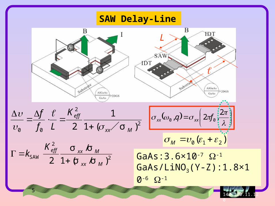
Sample under detectionSAW Delay-LineCoplanar Waveguide (CPW)
Basic scenario
5140.120.11.120
2
2
00 )/(1
1
2 Mxx
effK
Lf
f
σ
2
2
SAW )/(1
/
2 Mxx
MxxeffKk
σσσσ
L
)( 210 M
GaAs:3.6×10⁻⁷ -1
GaAs/LiNO3(Y-Z):1.8×10-6 -1
2
,2, 00 fq xxxx
SAW Delay-Line

6140.120.11.120
Electric field
50 meandering CPWtotal length s
xx
0,0 qxx
m2
12
eff
D
dG
Coplanar Waveguide (CPW)

7140.120.11.120
Some formulae about lossy CPW:
1m)()( CjGLjjj
m
F0 eff
LC ,
eff
r
C
LZ
0
00
11
m
12
12
eff
D
d
G
m
Np
2
m
rad
8
11
2
1
0
2 ln}Re{
Z
dDxx
Ls
sxx
L
Z
d
Zd
00
}Im{
8140.120.11.120
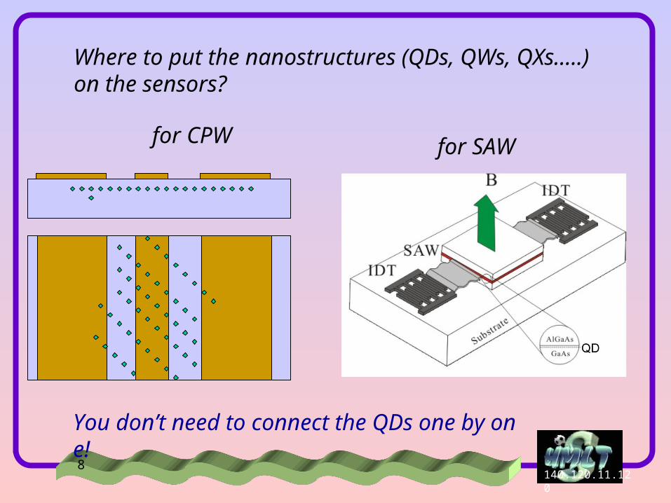
Where to put the nanostructures (QDs, QWs, QXs…..) on the sensors?
for CPW for SAW
You don’t need to connect the QDs one by one!
9140.120.11.120
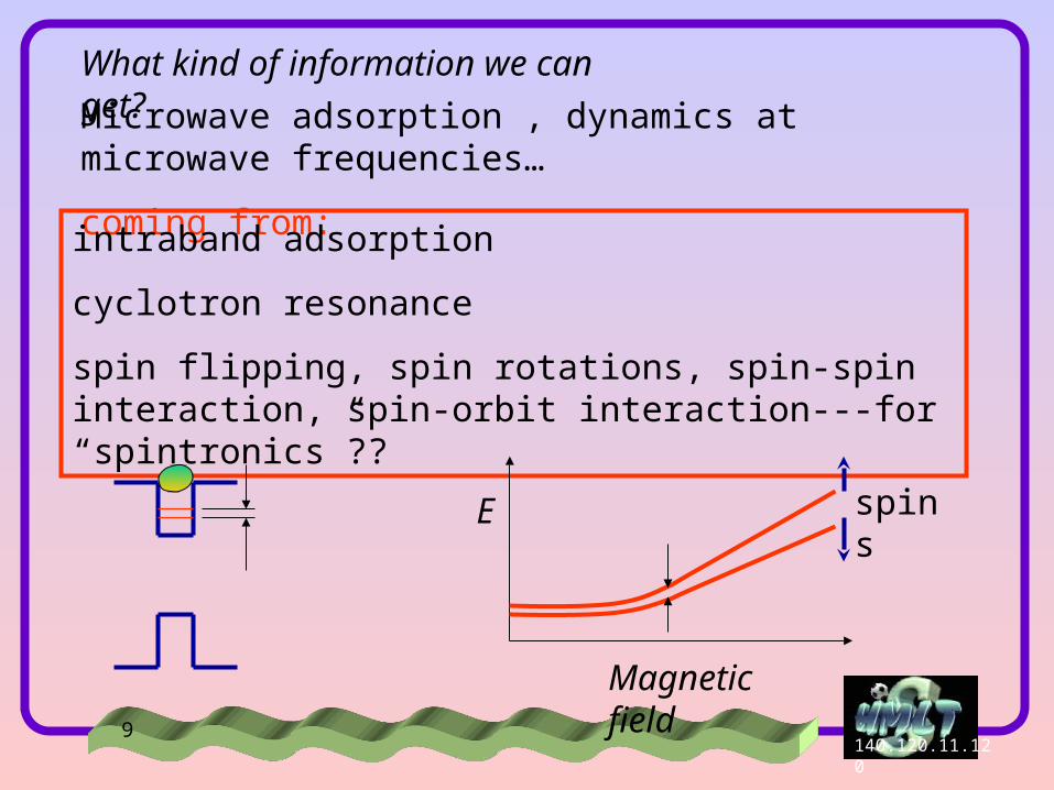
What kind of information we can get?
Microwave adsorption , dynamics at microwave frequencies…
coming from:
intraband adsorption
cyclotron resonance
spin flipping, spin rotations, spin-spin interaction, spin-orbit interaction---for “spintronics”??
spinsE
Magnetic field

10140.120.11.120
Schematic of a homemade PLL system for microwave signals up to 18 GHz.
FM
The phase resolution is about 0.001 degree even under very low average input power (~-100dBm).
A special designed homodyne amplitude detection scheme also allows us to detect very small microwave adsorption.

11140.120.11.120
A homodyne amplitude detection scheme
0º 90º
Ref. Signal (LO)
Signal from the sample
90º hybrid
Power splitter
mixerTo PLL
To amplitude detection
~0
A home-made vector meter??

12140.120.11.120
Why pulsed?
1. Use low average power to prevent from heating
2. Use gated averaging technique to avoid direct EM interruption
3. Avoid the reflection and multiple reflection signals

13140.120.11.120
Signal Gating & Averaging:
RF/Microwave pulse train
3~4 ms set by a lock-in amp
~200 s set by a pulse generator
0.2~2 s set by a pulse shaping circuit
s1(t)
s1(t)
sampling delay set by a pulse generator
sampling gate set by a pulse generatorfed into the controlling node of a sample-and-hold circuit
s3(t)
time delays2(t) signal of mixer
Direct coupled EMReflected signals s4(t) signal after SH
Peak power about –30~-70dBm
fed into lock-in
14140.120.11.120
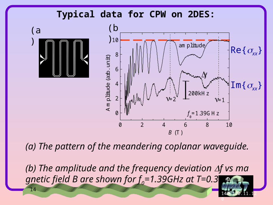
Typical data for CPW on 2DES:
0 2 4 6 8 10
0
2
4
6
8
10
Am
plitu
de (a
rb. u
nit)
200kHz=2 =1
f0=1.39GHz
B (T)
amplitude
f
(a) The pattern of the meandering coplanar waveguide. (b) The amplitude and the frequency deviation f vs magnetic field B are shown for f0=1.39GHz at T=0.3K.
(a) (b)
Re{xx}
Im{xx}

15140.120.11.120
0 2 4 6 8 10
f0=
T=0.3K
2.16G
=2 =1
1.74G
0.59G
0.96G
1.39G
500kHz
f
B (T)
2.92G
0 2 4 6 8 105
10
15
20
25
30
f0=
=2 =1
2.92G
2.16G
1.74G
1.39G
0.96G
0.59G
Am
plitu
de (
arb.
uni
t)
B (T)
More data:

16140.120.11.120
0.0 0.1 0.2 0.3 0.4 0.5 0.6-0.15
-0.10
-0.05
0.00
0.05
0.10
0.59GHz 0.96GHz 2.12GHz 2.92GHz
Im{
xx}
(e2 /h
)
Re{xx
} (e2/h)0.0 0.2 0.4 0.6 0.8
-0.15
-0.10
-0.05
0.00
0.05
0.10
0.15
0.96GHz
Im{
xx}
(e2 /h
)
Re{xx
} (e2/h)
2.12GHz 2.92GHz
0.59GHz
Some plots for scaling analysis

17140.120.11.120
Perspective
We have developed a potent and very sensitive tool for studying microwave properties of low-dimensional systems.
What Next?
Put CPW on substrate with nanostructures.
Put nanostructures on substrate with CPW.
Add bias or other excitations.


![Cloud Object Storage | Store & Retrieve Data Anywhere ... · 4 Table of contents = VQ \ IVL = +WUU]VQ\a++WUU]VQ\a WUU]VQ\a V Q \ = V Q \ 0MIT\Pa 0IJQ\[0MIT\Pa 0IJQ\[0 IT\Paa 0IJ](https://img.dokumen.tips/doc/110x75/5f87d6bf2b150f197f0c4a25/cloud-object-storage-store-retrieve-data-anywhere-4-table-of-contents.jpg)