Embed Size (px)
Citation preview
CONTACT [email protected]
WEBSITEii-vi.com Rev. 01
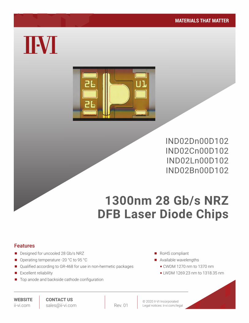
1300nm 28 Gb/s NRZ DFB Laser Diode Chips
Features
© 2020 II-VI IncorporatedLegal notices: ii-vi.com/legal
IND02Dn00D102IND02Cn00D102IND02Ln00D102IND02Bn00D102
Designed for uncooled 28 Gb/s NRZ
Operating temperature -20 °C to 95 °C
Qualified according to GR-468 for use in non-hermetic packages
Excellent reliability
Top anode and backside cathode configuration
RoHS compliant
Available wavelengths CWDM 1270 nm to 1370 nm LWDM 1269.23 nm to 1318.35 nm

1300nm 28 Gb/s NRZ DFB Laser Diode Chips
Electro-Optical CharacteristicsOperating conditions: Top= -20° to 95°C
Designed for uncooled 28 Gb/s NRZ
Operating temperature -20 °C to 95 °C
Qualified according to GR-468 for use in non-hermetic packages
Excellent reliability
Top anode and backside cathode configuration
RoHS compliant
Available wavelengths CWDM 1270 nm to 1370 nm LWDM 1269.23 nm to 1318.35 nm
Treshold current
Slope efficiency
Slope efficiency ratio
Saturation current
Operating voltage
Differential resistance
Capacitance
Front/Back output power ratio
Side mode suppression ratio
Wavelength
Wavelength temperature
coefficient
Thermal Impedance
Beam divergence (Horizontal)
Beam divergence (Vertical)
Relative intensity noise
Bandwidth
Relaxation oscillation frequency
Ith
SE
SE0C/SE85C
lsat
Vf
R
C
Pf/Pb
SMSR
λ
dλ /dt
Zth
ΘH
ΘV
RIN
f3db
fr
mA
W/A
mA
V
Ohm
pF
dB
nm/°C
K/W
degree
degree
dB/Hz1/2
GHz
GHz
0.1
80
7
35
18
15.5
11
5
0.2
100
7
1.2
0.09
140
30
35
21
17.5
17
4
1.6
10
60
-132
Min Typ Max
85°C
25°C
85°C
0°C, 85°C
85°C
Po = 5 mW
Po = 5 mW, 85°C
Po = 5 mW
see table below
FWHM
FWHM
Po = 5 mW
I = 60 mA, 85°C
I = 60 mA, 85°C
Parameter Symbol UnitConditions
Applications Fiber optical communication links
Gigabit Ethernet and storage area networks
5G Wireless front-haul datalinks
Shipment packaging options Diced wafer on UV tape with grip ring Ø 150mm
2/22/4
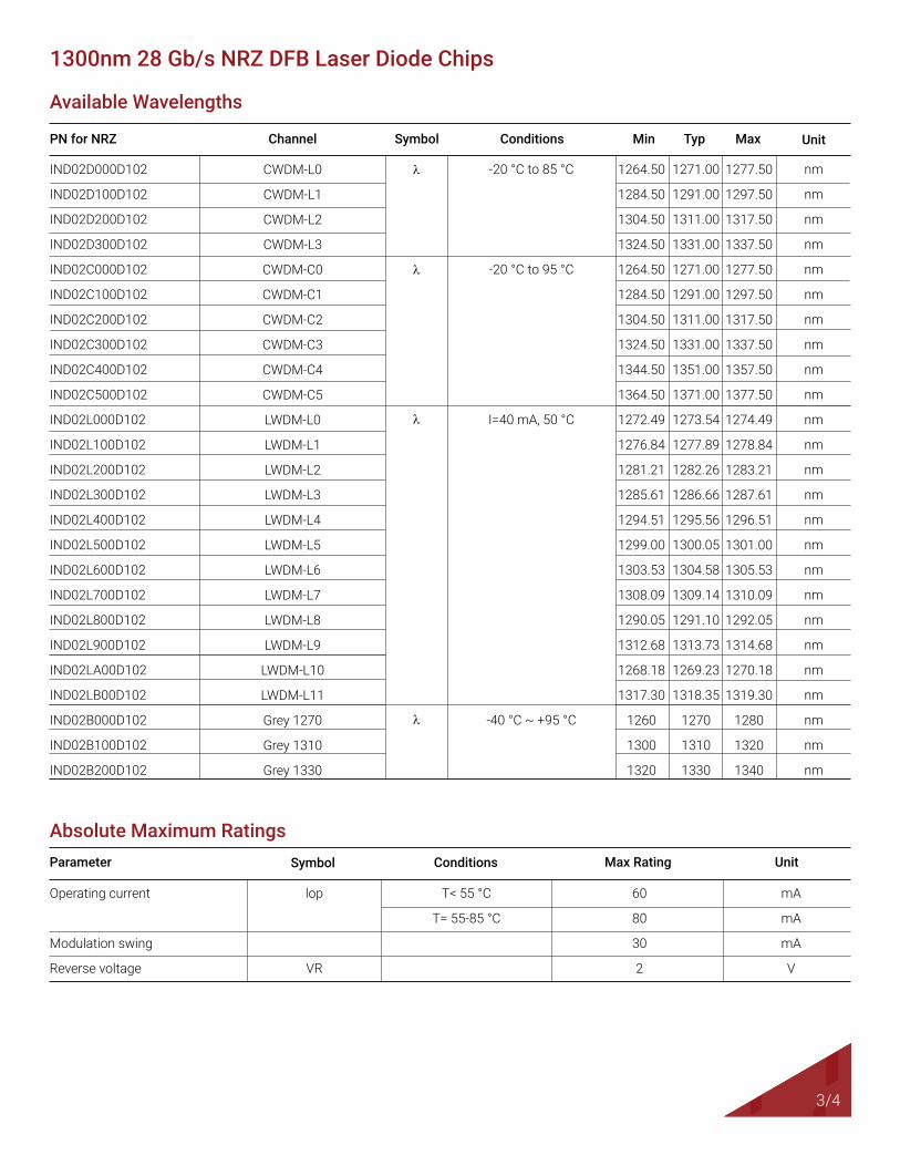
Absolute Maximum Ratings
Operating current
Modulation swing
Reverse voltage
60
80
30
2
mA
mA
mA
V
Parameter Max Rating UnitSymbol Conditions
lop
VR
T< 55 °C
T= 55-85 °C
-20 °C to 85 °C
-20 °C to 95 °C
I=40 mA, 50 °C
-40 °C ~ +95 °C
Min Typ MaxPN for NRZ SymbolChannel UnitConditions
λ
λ
nm
nm
nm
nm
nm
nm
nm
nm
nm
nm
nm
nm
nm
nm
nm
nm
nm
nm
nm
nm
nm
nm
nm
nm
nm
λ
λ
IND02D000D102
IND02D100D102
IND02D200D102
IND02D300D102
IND02C000D102
IND02C100D102
IND02C200D102
IND02C300D102
IND02C400D102
IND02C500D102
IND02L000D102
IND02L100D102
IND02L200D102
IND02L300D102
IND02L400D102
IND02L500D102
IND02L600D102
IND02L700D102
IND02L800D102
IND02L900D102
IND02LA00D102
IND02LB00D102
IND02B000D102
IND02B100D102
IND02B200D102
1271.00
1291.00
1311.00
1331.00
1271.00
1291.00
1311.00
1331.00
1351.00
1371.00
1273.54
1277.89
1282.26
1286.66
1295.56
1300.05
1304.58
1309.14
1291.10
1313.73
1269.23
1318.35
1270
1310
1330
1264.50
1284.50
1304.50
1324.50
1264.50
1284.50
1304.50
1324.50
1344.50
1364.50
1272.49
1276.84
1281.21
1285.61
1294.51
1299.00
1303.53
1308.09
1290.05
1312.68
1268.18
1317.30
1260
1300
1320
1277.50
1297.50
1317.50
1337.50
1277.50
1297.50
1317.50
1337.50
1357.50
1377.50
1274.49
1278.84
1283.21
1287.61
1296.51
1301.00
1305.53
1310.09
1292.05
1314.68
1270.18
1319.30
1280
1320
1340
CWDM-L0
CWDM-L1
CWDM-L2
CWDM-L3
CWDM-C0
CWDM-C1
CWDM-C2
CWDM-C3
CWDM-C4
CWDM-C5
LWDM-L0
LWDM-L1
LWDM-L2
LWDM-L3
LWDM-L4
LWDM-L5
LWDM-L6
LWDM-L7
LWDM-L8
LWDM-L9
LWDM-L10
LWDM-L11
Grey 1270
Grey 1310
Grey 1330
1300nm 28 Gb/s NRZ DFB Laser Diode Chips
Available Wavelengths
2/23/4
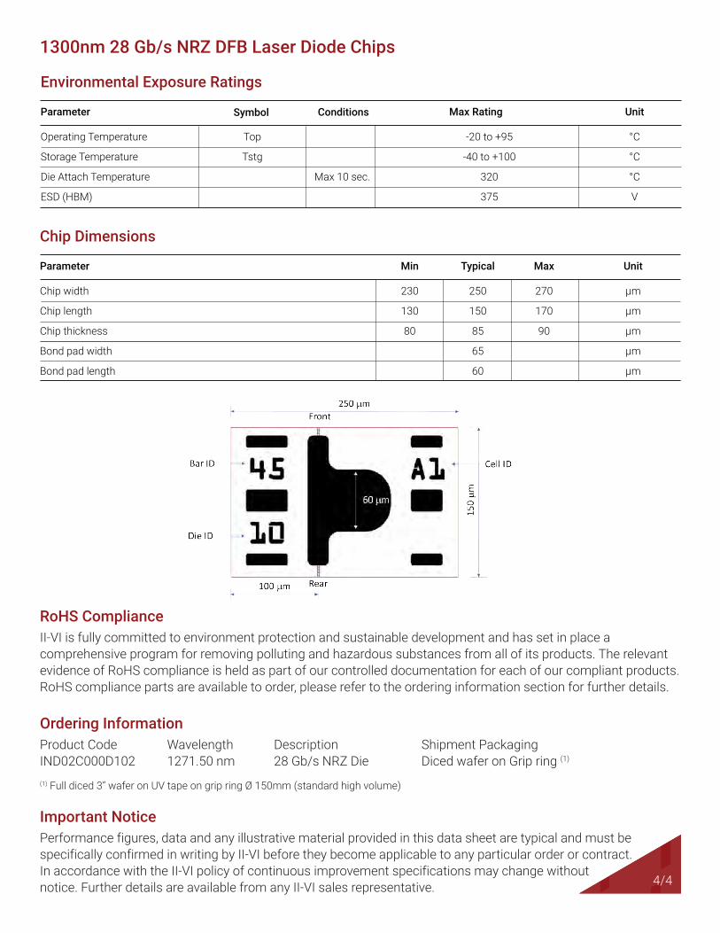
Chip width
Chip length
Chip thickness
Bond pad width
Bond pad length
250
150
85
65
60
270
170
90
230
130
80
µm
µm
µm
µm
µm
Parameter Min Typical Max Unit
Chip Dimensions
Environmental Exposure Ratings
II-VI is fully committed to environment protection and sustainable development and has set in place a comprehensive program for removing polluting and hazardous substances from all of its products. The relevant evidence of RoHS compliance is held as part of our controlled documentation for each of our compliant products. RoHS compliance parts are available to order, please refer to the ordering information section for further details.
RoHS Compliance
Performance figures, data and any illustrative material provided in this data sheet are typical and must be specifically confirmed in writing by II-VI before they become applicable to any particular order or contract. In accordance with the II-VI policy of continuous improvement specifications may change without notice. Further details are available from any II-VI sales representative.
Important Notice
Product Code Wavelength Description Shipment Packaging IND02C000D102 1271.50 nm 28 Gb/s NRZ Die Diced wafer on Grip ring (1)
(1) Full diced 3’’ wafer on UV tape on grip ring Ø 150mm (standard high volume)
Ordering Information
Operating Temperature
Storage Temperature
Die Attach Temperature
ESD (HBM)
-20 to +95
-40 to +100
320
375
°C
°C
°C
V
Parameter Max Rating UnitSymbol Conditions
Top
Tstg
Max 10 sec.
1300nm 28 Gb/s NRZ DFB Laser Diode Chips
2/24/4


![CHAPTER-4 Line Codes RZ: Return to Zero [ pulse for half ... · NRZ . Return to Zero[ pulse for full duration of T. b ] Unipolar (NRZ) Unipolar NRZ . NRZ-inverted (differential](https://img.dokumen.tips/doc/110x75/5cc1fa9b88c9933e3a8d2cb0/chapter-4-line-codes-rz-return-to-zero-pulse-for-half-nrz-return-to.jpg)