Embed Size (px)
Citation preview
1
Day 13
Boolean Algebra
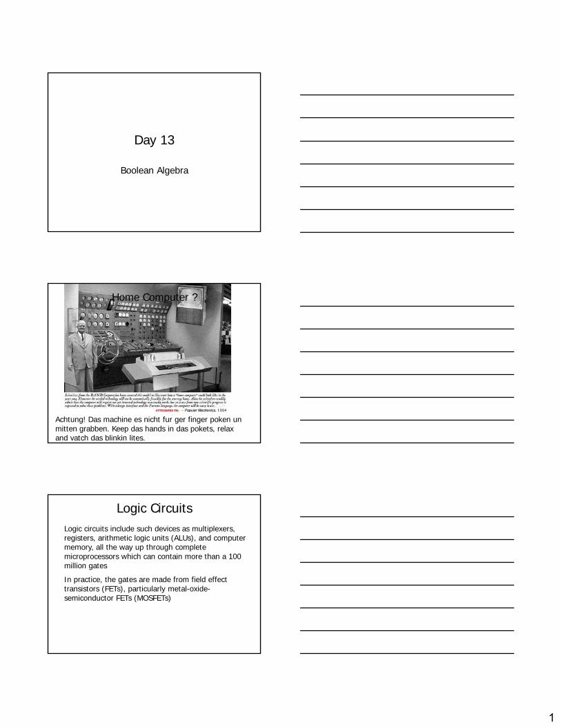
Actually a submarine training console
Do not believe everything you see
Home Computer ?
Achtung! Das machine es nicht fur ger finger poken un mitten grabben. Keep das hands in das pokets, relax and vatch das blinkin lites.
Logic CircuitsLogic circuits include such devices as multiplexers, registers, arithmetic logic units (ALUs), and computer memory, all the way up through complete microprocessors which can contain more than a 100 million gates
In practice, the gates are made from field effect transistors (FETs), particularly metal-oxide-semiconductor FETs (MOSFETs)
2
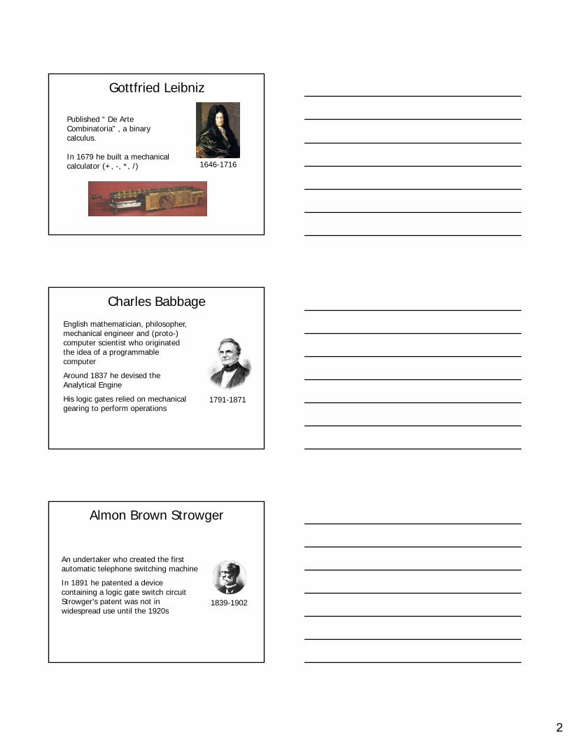
Gottfried Leibniz
Published “ De Arte Combinatoria” , a binary calculus.
I 1679 h b ilt h i lIn 1679 he built a mechanical calculator (+, -, *, /) 1646-1716
Charles Babbage
English mathematician, philosopher, mechanical engineer and (proto-) computer scientist who originated the idea of a programmable computer
1791-1871
Around 1837 he devised the Analytical Engine
His logic gates relied on mechanical gearing to perform operations
Almon Brown Strowger
An undertaker who created the first automatic telephone switching machine
In 1891 he patented a deviceIn 1891 he patented a device containing a logic gate switch circuit Strowger's patent was not in widespread use until the 1920s
1839-1902
3
Logic GateA logic gate performs a logical operation on one or more logic inputs and produces a single logic output
The logic normally performed is Boolean logic and is most commonly found in digital circuits.
All logic circuits are equivalent to Boolean expressions and any Boolean expression can be rendered as a logic circuit
Logic gates are primarily implemented electronically using diodes or transistors, but can also be constructed using electromagnetic relays, fluidics, optical or even mechanical elements
Logic Gate
A Boolean logical input or output always takes one of two logic levels
These logic levels can go by many names including: g g y y g
on / off high (H) / low (L)
one (1) / zero (0) true (T) / false (F)
positive / negative positive / ground
open circuit / close circuit, yes / no
Logic GateA logic gate takes one or more logic-level inputs and produces a single logic-level output
Because the output is also a logic level, an output of one logic gate can connect to the input of one or more other logic gates
There are several different families of logic gates
Each family has its capabilities and limitations, its advantages and disadvantages
4
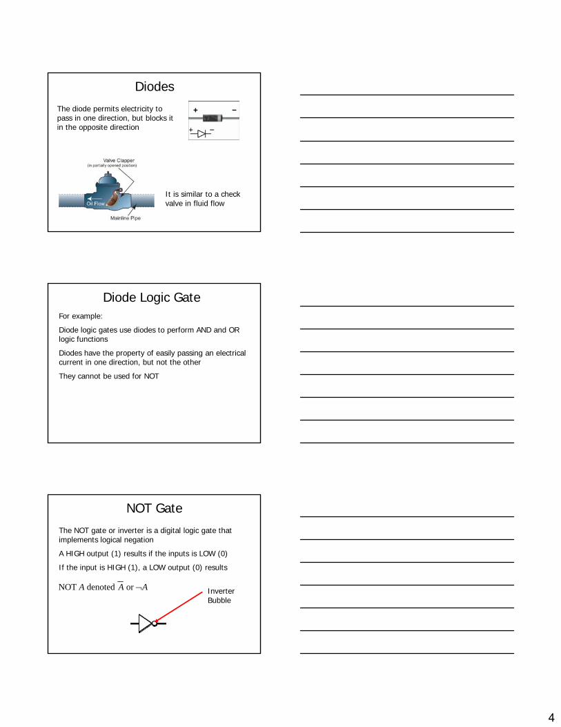
Diodes
The diode permits electricity to pass in one direction, but blocks it in the opposite direction
It is similar to a check valve in fluid flow
Diode Logic GateFor example:
Diode logic gates use diodes to perform AND and OR logic functions
Diodes have the property of easily passing an electrical current in one direction but not the othercurrent in one direction, but not the other
They cannot be used for NOT
NOT Gate
The NOT gate or inverter is a digital logic gate that implements logical negation
A HIGH output (1) results if the inputs is LOW (0)
If the input is HIGH (1), a LOW output (0) results
NOT denoted or A A A¬ Inverter Bubble
5
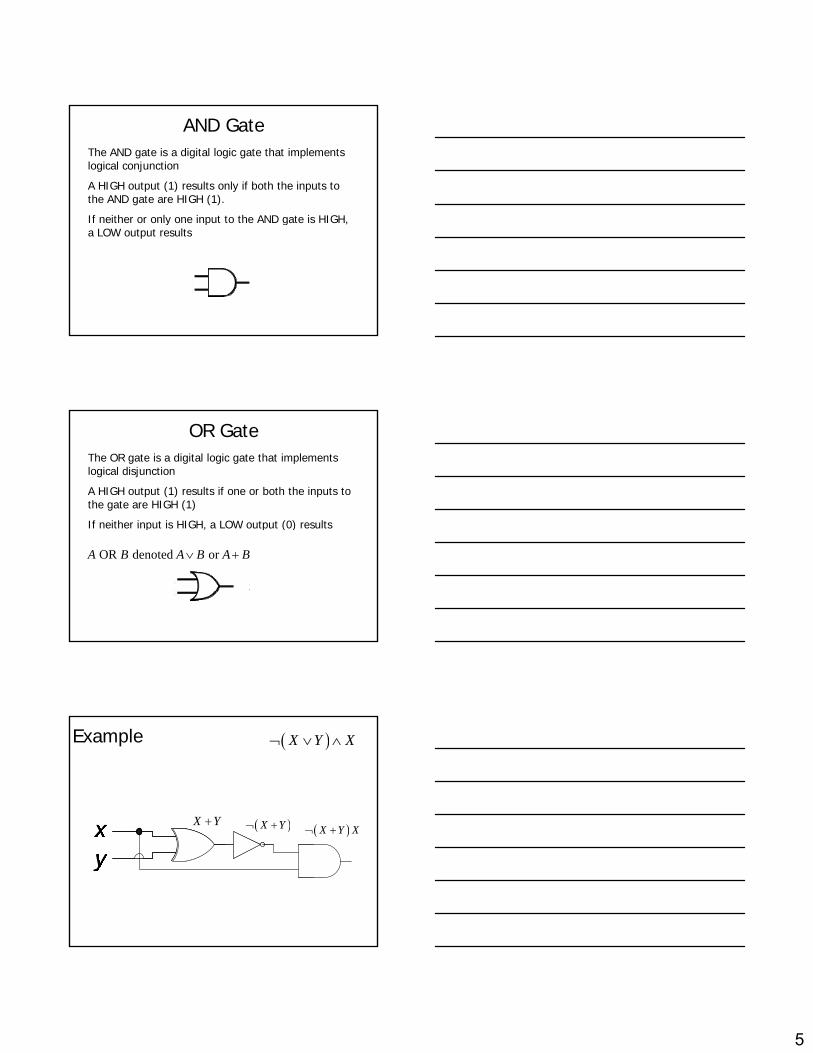
AND GateThe AND gate is a digital logic gate that implements logical conjunction
A HIGH output (1) results only if both the inputs to the AND gate are HIGH (1).
If neither or only one input to the AND gate is HIGHIf neither or only one input to the AND gate is HIGH, a LOW output results
AND denoted or A B A B AB∧
OR GateThe OR gate is a digital logic gate that implements logical disjunction
A HIGH output (1) results if one or both the inputs to the gate are HIGH (1)
If neither input is HIGH a LOW output (0) resultsIf neither input is HIGH, a LOW output (0) results
OR denoted or A B A B A B∨ +
Example
x
( )X Y X¬ ∨ ∧
( )X Y¬ +X Y+( )X Y X¬ +x
y( ) ( )X Y X¬ +
6
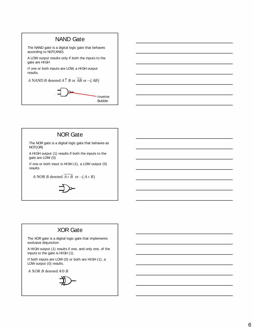
NAND GateThe NAND gate is a digital logic gate that behaves according to NOT(AND)
A LOW output results only if both the inputs to the gate are HIGH
If one or both inputs are LOW a HIGH outputIf one or both inputs are LOW, a HIGH output results.
( ) NAND denoted or or A B A B AB AB↑ ¬
Inverter Bubble
NOR GateThe NOR gate is a digital logic gate that behaves as NOT(OR)
A HIGH output (1) results if both the inputs to the gate are LOW (0)
If one or both input is HIGH (1) a LOW output (0)If one or both input is HIGH (1), a LOW output (0) results
( ) NOR denoted or A B A B A B+ ¬ +
XOR GateThe XOR gate is a digital logic gate that implements exclusive disjunction
A HIGH output (1) results if one, and only one, of the inputs to the gate is HIGH (1).
If both inputs are LOW (0) or both are HIGH (1) aIf both inputs are LOW (0) or both are HIGH (1), a LOW output (0) results.
XOR denoted A B A B⊗
7
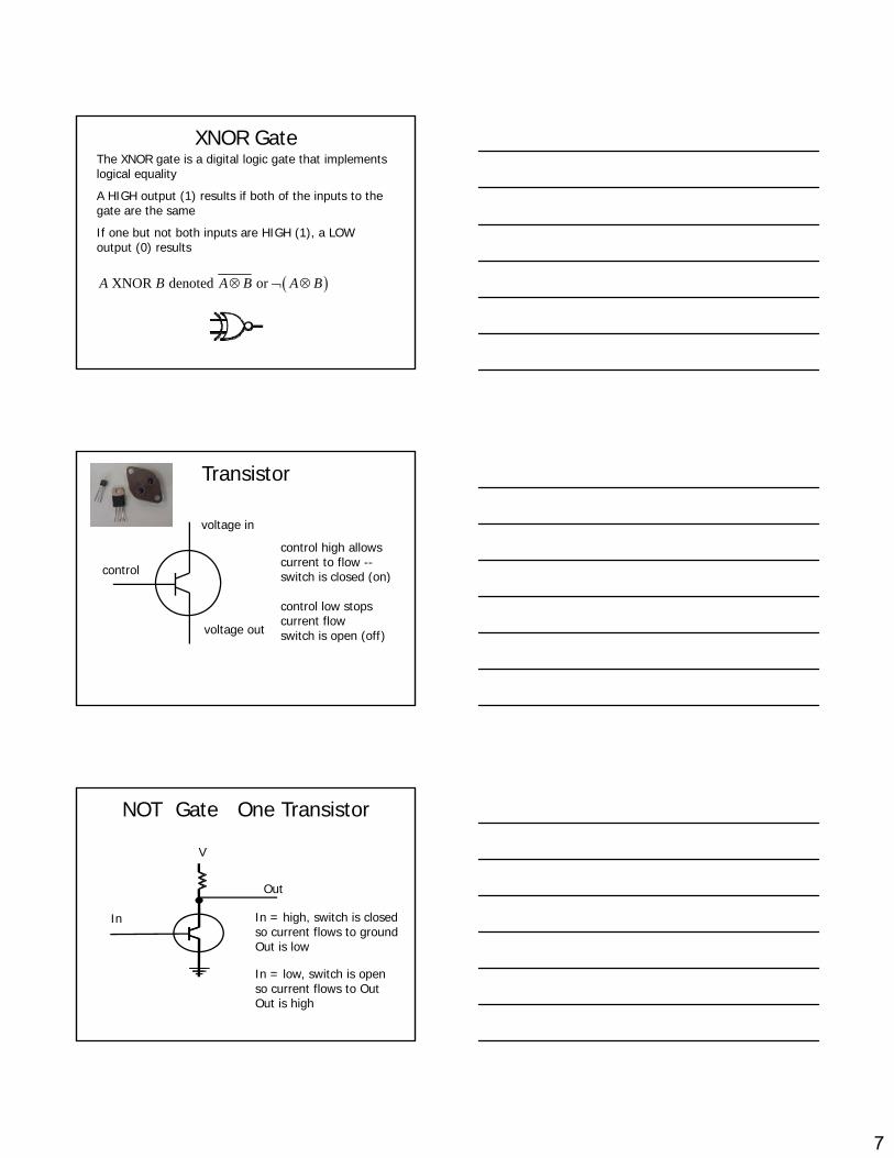
XNOR GateThe XNOR gate is a digital logic gate that implements logical equality
A HIGH output (1) results if both of the inputs to the gate are the same
If one but not both inputs are HIGH (1), a LOW (0) loutput (0) results
( ) XNOR denoted or A B A B A B⊗ ¬ ⊗
Transistor
control
voltage in
control high allowscurrent to flow --switch is closed (on)
voltage out
switch is closed (on)
control low stops current flowswitch is open (off)
NOT Gate One Transistor
I
Out
I hi h it h i l d
V
In In = high, switch is closedso current flows to ground Out is low
In = low, switch is openso current flows to Out Out is high
8
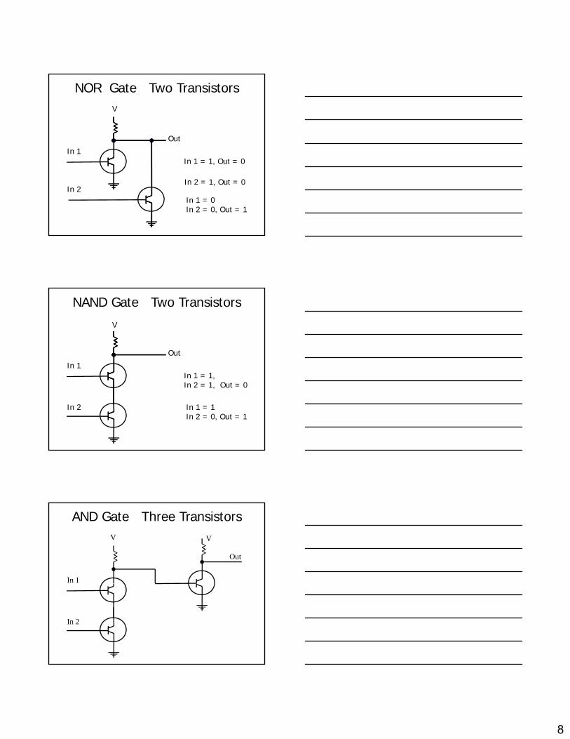
NOR Gate Two Transistors
In 1
Out
V
In 2
In 1 = 1, Out = 0
In 2 = 1, Out = 0
In 1 = 0In 2 = 0, Out = 1
NAND Gate Two Transistors
In 1
Out
V
In 2
In 1 = 1, In 2 = 1, Out = 0
In 1 = 1In 2 = 0, Out = 1
AND Gate Three Transistors
In 1
V
Out
V
In 2
9
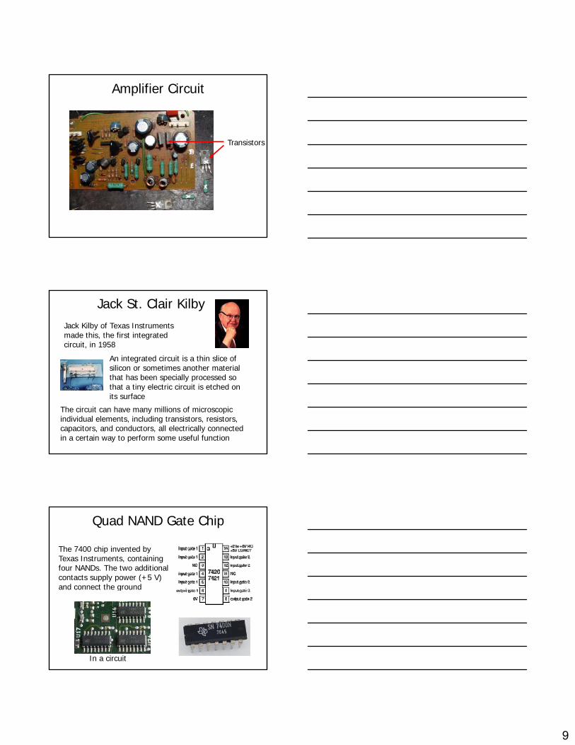
Amplifier Circuit
Transistors
Jack St. Clair Kilby Jack Kilby of Texas Instruments made this, the first integrated circuit, in 1958
An integrated circuit is a thin slice of silicon or sometimes another material that has been specially processed so that a tiny electric circuit is etched on its surface
The circuit can have many millions of microscopic individual elements, including transistors, resistors, capacitors, and conductors, all electrically connected in a certain way to perform some useful function
Quad NAND Gate Chip
The 7400 chip invented by Texas Instruments, containing four NANDs. The two additional contacts supply power (+5 V) and connect the groundand connect the ground
In a circuit
10
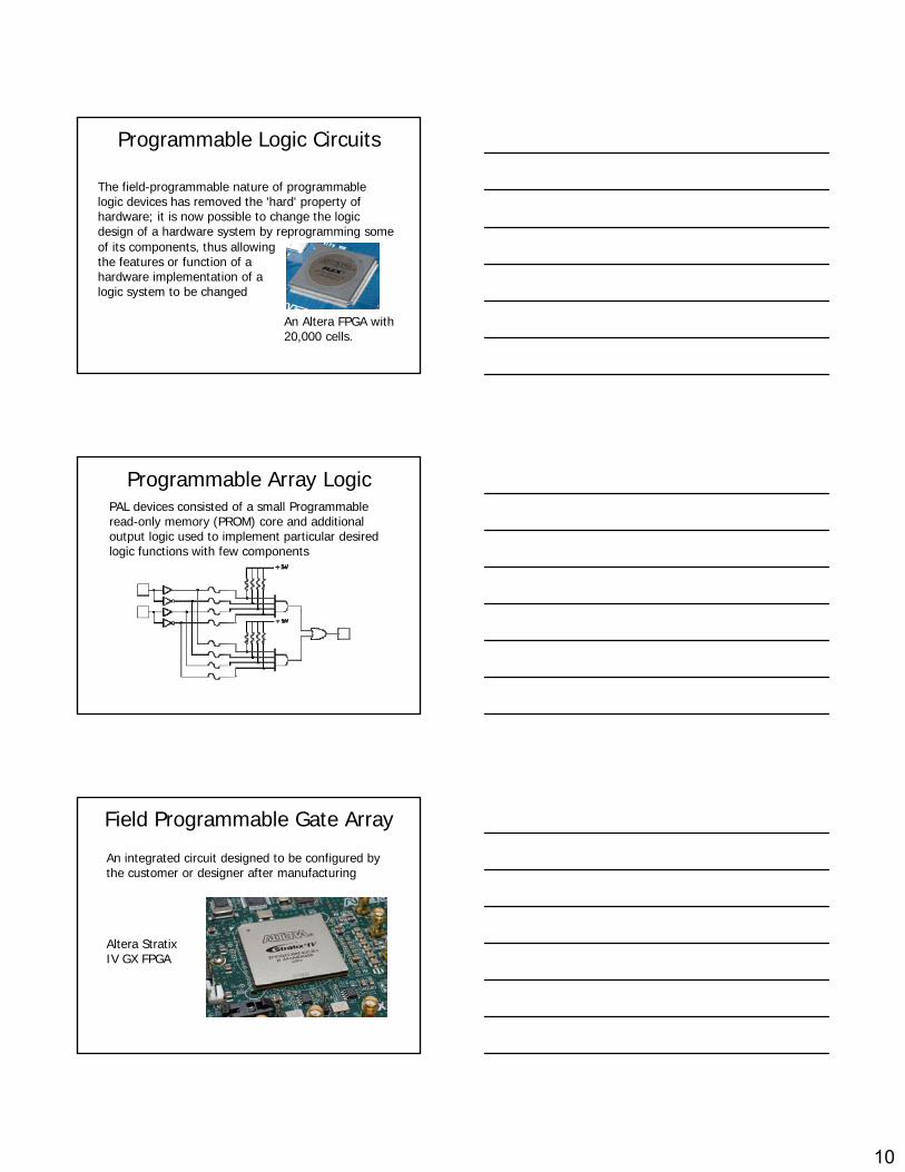
Programmable Logic Circuits
The field-programmable nature of programmable logic devices has removed the 'hard' property of hardware; it is now possible to change the logic design of a hardware system by reprogramming someof its components thus allowing
An Altera FPGA with 20,000 cells.
of its components, thus allowing the features or function of a hardware implementation of a logic system to be changed
Programmable Array LogicPAL devices consisted of a small Programmable read-only memory (PROM) core and additional output logic used to implement particular desired logic functions with few components
Field Programmable Gate Array
An integrated circuit designed to be configured by the customer or designer after manufacturing
Altera Stratix IV GX FPGA
11
Complex Programmable Logic Device
A programmable logic device with complexity between that of PALs and FPGAs, and architectural f t f b thfeatures of both
Altera MAX 7000-series CPLD with 2500 gate
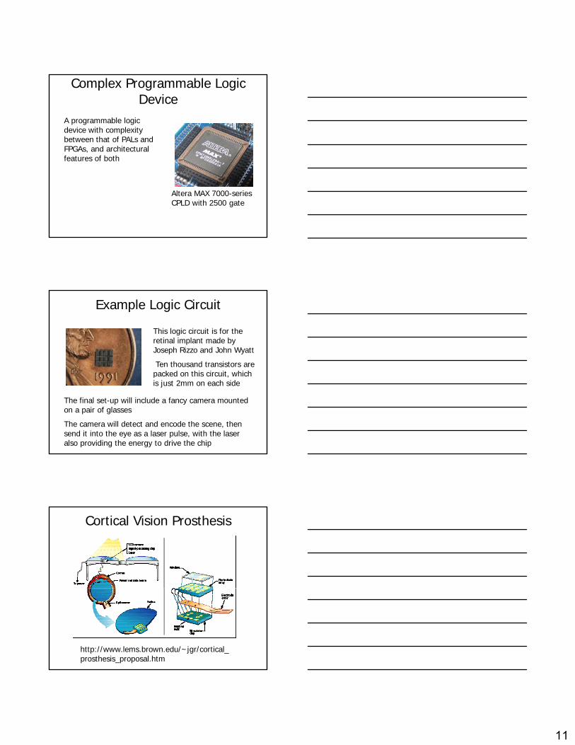
Example Logic Circuit
This logic circuit is for the retinal implant made by Joseph Rizzo and John Wyatt
Ten thousand transistors are packed on this circuit whichpacked on this circuit, which is just 2mm on each side
The final set-up will include a fancy camera mounted on a pair of glasses
The camera will detect and encode the scene, then send it into the eye as a laser pulse, with the laser also providing the energy to drive the chip
Cortical Vision Prosthesis
http://www.lems.brown.edu/~jgr/cortical_prosthesis_proposal.htm
12
NAND and NOR Gates
NAND or NOR gates can be combined to create any type of gate
This enables a circuit to be built from just one type of gate, either NAND or NOR
AND and OR gates cannot be used to create other gates because they lack the inverting (NOT) function
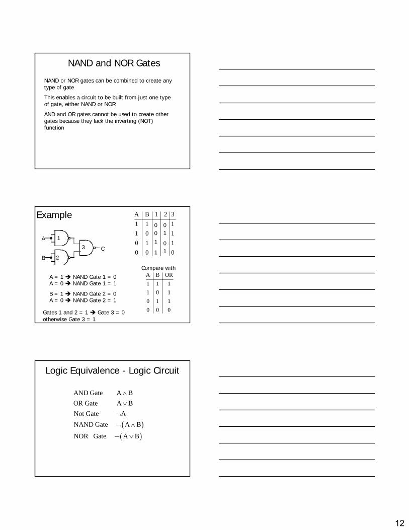
Example
A
B
C
A B 1 21 11 00 10 0
1
2
3
00
1
1
01
3 1110
01
A = 1 NAND Gate 1 = 0A = 0 NAND Gate 1 = 1
B = 1 NAND Gate 2 = 0A = 0 NAND Gate 2 = 1
Gates 1 and 2 = 1 Gate 3 = 0otherwise Gate 3 = 1
A B OR1 1 11 0 10 1 10 0 0
Compare with
Logic Equivalence - Logic Circuit
AND Gate A BOR Gate A BNot Gate A
∧∨
¬
( )( )
NAND Gate A B
NOR Gate A B
¬ ∧
¬ ∨
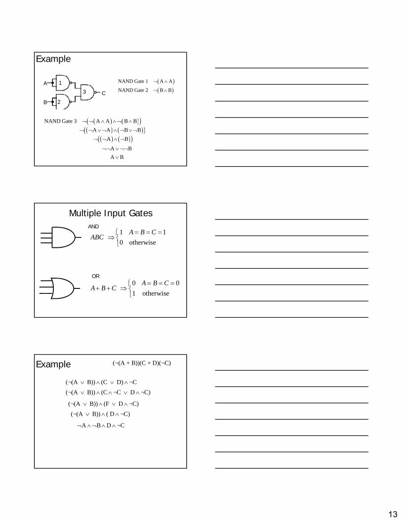
13
A
B
C
1
2
3
( )( )
NAND Gate 1 A A
NAND Gate 2 B B
¬ ∧
¬ ∧
Example
( ) ( )( )NAND Gate 3 A A B B¬ ¬ ∧ ∧¬ ∧
( ) ( )( )A A B B¬ ¬ ∨¬ ∧ ¬ ∨¬
( ) ( )( )A B¬ ¬ ∧ ¬
A B¬¬ ∨¬¬A B∨
Multiple Input Gates
1 1
0 otherwise A B C
ABC= = =⎧
⇒ ⎨⎩
AND
0 0
1 otherwise A B C
A B C= = =⎧
+ + ⇒ ⎨⎩
OR
Example (¬(A + B))(C + D)(¬C)
(¬(A B)) (C D) ¬C∨ ∧ ∨ ∧
(¬(A B)) (C ¬C D ¬C)∨ ∧ ∧ ∨ ∧
(¬(A B)) (F D ¬C)∨ ∧ ∨ ∧
(¬(A B)) ( D ¬C)∨ ∧ ∧
A B D ¬C¬ ∧¬ ∧ ∧
14
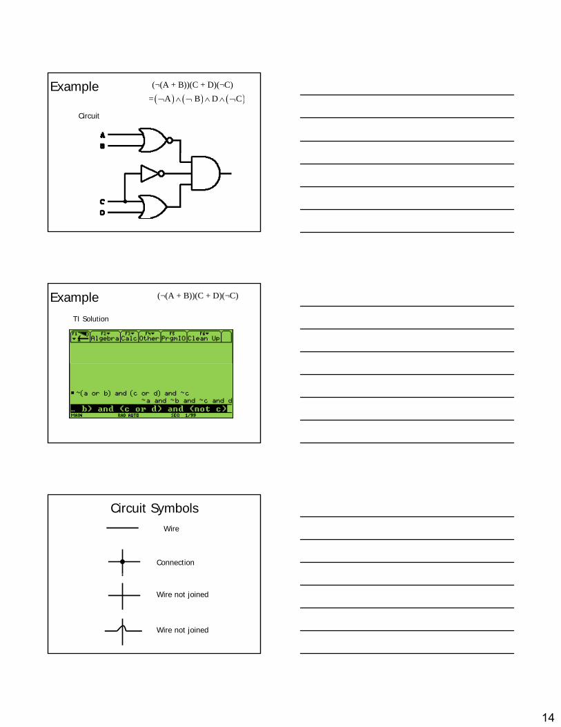
Example (¬(A + B))(C + D)(¬C)
( ) ( ) ( )= A B D C¬ ∧ ¬ ∧ ∧ ¬
Circuit
TI Solution
Example (¬(A + B))(C + D)(¬C)
Circuit SymbolsWire
Connection
Wire not joined
Wire not joined
15
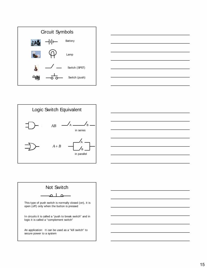
Circuit Symbols
Battery
Lamp
Switch (SPST)
Switch (push)
Logic Switch Equivalent
And A B ABin series
Or
A
B A B+
in parallel
Not Switch
This type of push switch is normally closed (on), it is open (off) only when the button is pressed
In circuits it is called a “push to break switch” and in logic it is called a “complement switch”
An application: It can be used as a “kill switch” to secure power to a system
16
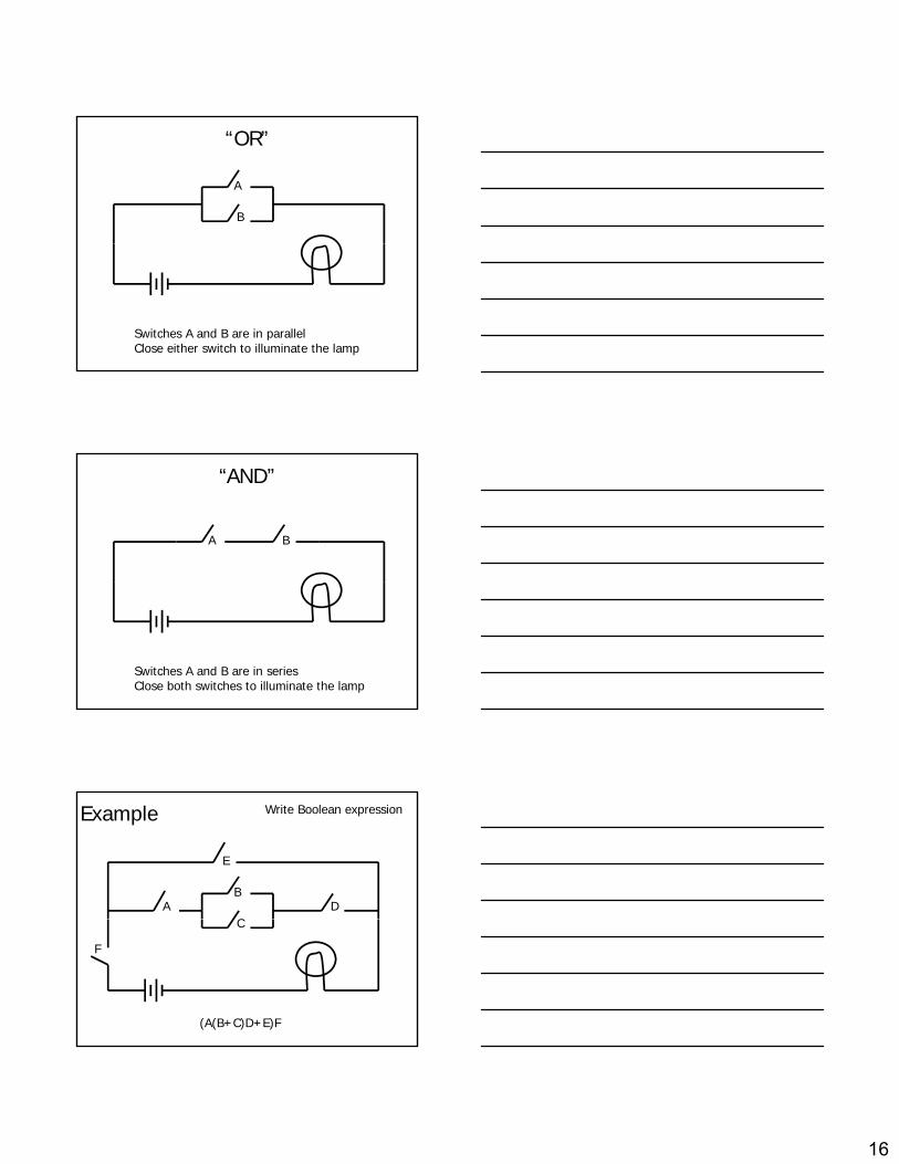
“OR”
A
B
Switches A and B are in parallelClose either switch to illuminate the lamp
“AND”
A B
Switches A and B are in seriesClose both switches to illuminate the lamp
Example
A D B
C
Write Boolean expression
E
(A(B+C)D+E)F
C
F
17
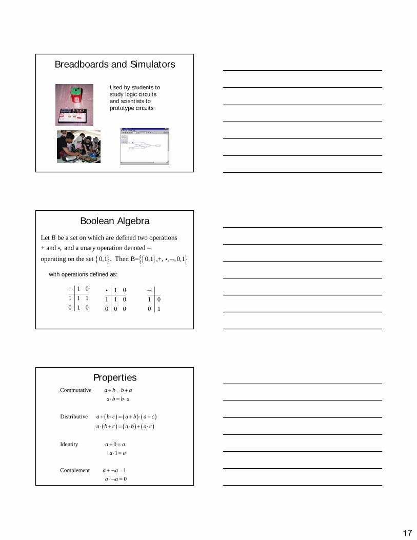
Breadboards and Simulators
Used by students to study logic circuitsand scientists to prototype circuits
Boolean Algebra
{ } { }{ }
Let be a set on which are defined two operations+ and , and a unary operation denoted
operating on the set 0,1 . Then B= 0,1 ,+, , ,0,1
B¬
¬
ii
1 01 1 10 1 0
+
with operations defined as:
1 01 1 00 0 0
i1 00 1
¬
Properties
( ) ( ) ( )( ) ( ) ( )
Commutative
Distributive
a b b aa b b a
a b c a b a c
a b c a b a c
+ = +⋅ = ⋅
+ ⋅ = + ⋅ +
⋅ + = ⋅ + ⋅( ) ( ) ( )
Identity 0
a b c a b a c
a a
⋅ + = ⋅ + ⋅
+ = 1
Complement 1 0
a a
a aa a
⋅ =
+¬ =⋅¬ =
18
Example ( ) ( )Simplify AB A B C B B C+ + + +
AB AB AC BB BC+ + + + Distributive Law
AB AC B BC+ + +
BB B=AB AB AC B BC+ + + +
AB AB AB+ =AB AC B BC+ + +
( )1AB AC B C+ + + Distributive Law
AB AC B+ + 1 1C+ =
( )1AC B A+ + Distributive Law
AC B+ 1 1A+ =
Remarks
We may denote as and as or a b ab a a a′⋅ ¬The 0 element if called the zero elementthe 1 element is called the unit element
is called the complement of a a¬The operation is called the sumThen operation is called the product
+⋅
Unless guide by parentheses, the order of precedence is ¬ ⋅ +
Duality PrincipleAny algebraic equality derived from the axioms of Boolean algebra remains true when the operators “OR” and “AND” are interchanged and the identity elements “0” and “1” are interchanged
This property is called the duality principlep p y y p p
For example:x + 1 = 1x * 0 = 0 (dual)
Because of the duality principle, for any given theorem we get it's dual for free
19
Remarks
In a Boolean algebra, the element x is unique
1 and 0x y xy y x+ = = ⇒ =
Properties of a Boolean Algebra
Idempotent Laws
Bound Laws 1 0 0
x x x xx x
x x x
+ = =
+ = =
( )Absorption Laws x xy x x x y x+ = + =
Graphic Representation
0
1
A A
A A
⋅ =
+ =A
A
Full square = complete set =1
Yellow part = NOT(A) = AWhite circle = A
20
( )Involution Law
0 and 1 Laws 0 1 1 0
x x=
= =
Properties of a Boolean Algebra
De Morgan's Laws y x x x xy x y+ = = +
De Morgan’s Law
( )p q p q¬ ∨ = ¬ ∧¬( )p q p q∧ ∨
Boolean Notation
Logic Notation
p q p q= +
p q p q+ =
( )p q p q¬ ∧ = ¬ ∨¬
We can use this law and other properties when constructing logic circuits to substitute gates for either gates on hand, or less expensive gates
( )p q p q¬ ∪ = ¬ ∩¬( )p q p q¬ ∩ = ¬ ∪¬
Set Notation
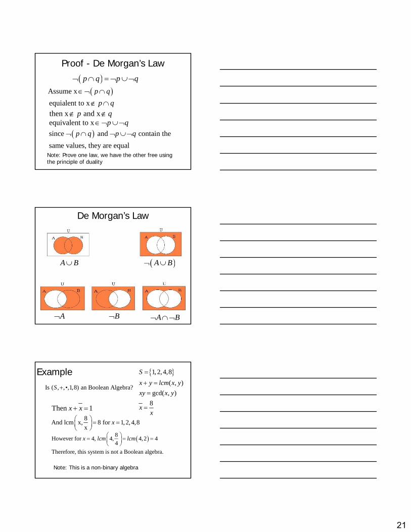
Proof - De Morgan’s Law
equivalent to x p q∉ ∪
( )p q p q¬ ∪ = ¬ ∩¬
then x and xp q∉ ∉so x p q∉ ∩
Assume x p q∈¬ ∪
so x p q∉ ∩equivalent to x p q∈¬ ∩¬
( )since and contain the same values, they are equal
p q p q¬ ∪ ¬ ∩¬
Note: We could have used truth tables to show this
21
Proof - De Morgan’s Law
( )p q p q¬ ∩ = ¬ ∪¬
( )Assume x p q∈¬ ∩
equialent to x p q∉ ∩th dthen x and xp q∉ ∉equivalent to x p q∈¬ ∪¬
( )since and contain the same values, they are equal
p q p q¬ ∩ ¬ ∪¬
Note: Prove one law, we have the other free usingthe principle of duality
De Morgan’s Law
A B∪ ( )A B¬ ∪
A¬ B¬ A B¬ ∩¬
( )
Example { }1,2,4,8( , )
gcd( , )8
Sx y lcm x yxy x y
xx
=
+ ==
=
Is ( , , •,1,8) an Boolean Algebra?S +
Then 1x x+ =8A d l 8 f 1 2 4 8⎛ ⎞
( )8However for 4, 4, 4,2 44
Therefore, this system is not a Boolean algebra.
x lcm lcm⎛ ⎞= = =⎜ ⎟⎝ ⎠
8And lcm x, 8 for 1,2, 4,8x
x⎛ ⎞ = =⎜ ⎟⎝ ⎠
Note: This is a non-binary algebra
22
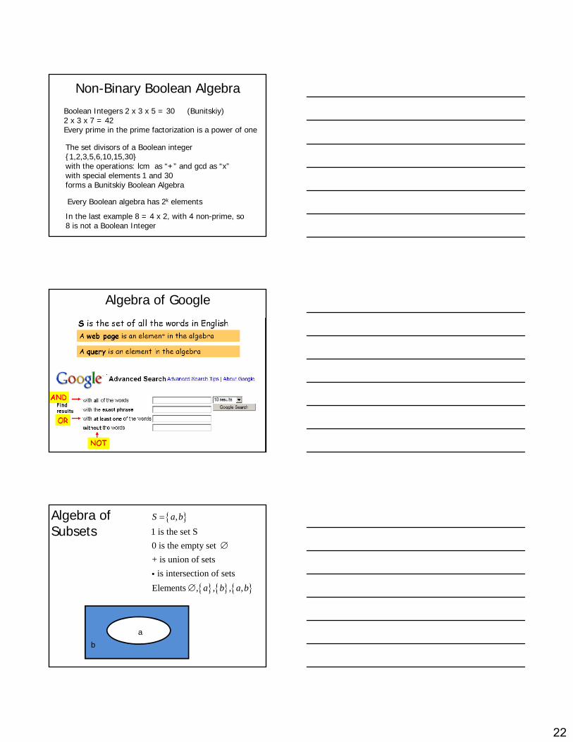
Non-Binary Boolean Algebra
Boolean Integers 2 x 3 x 5 = 30 (Bunitskiy)2 x 3 x 7 = 42Every prime in the prime factorization is a power of one
The set divisors of a Boolean integer{1 2 3 5 6 10 15 30}{1,2,3,5,6,10,15,30}with the operations: lcm as “+” and gcd as “x”with special elements 1 and 30forms a Bunitskiy Boolean Algebra
In the last example 8 = 4 x 2, with 4 non-prime, so 8 is not a Boolean Integer
Every Boolean algebra has 2k elements
Algebra of Google
Algebra of Subsets
{ }
{ } { } { }
,1 is the set S0 is the empty set + is union of sets is intersection of sets
El t
S a b
b b
=
∅
∅
i{ } { } { }Elements , , , ,a b a b∅
a
b
23
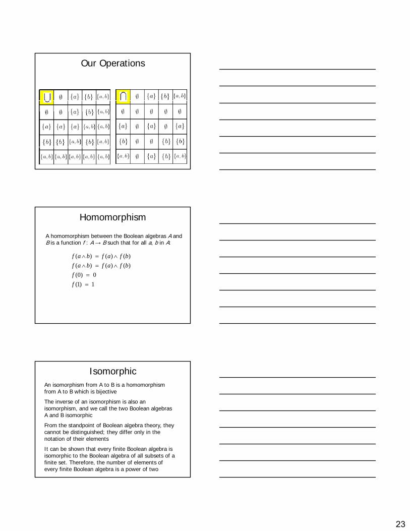
Our Operations
Homomorphism
A homomorphism between the Boolean algebras A and B is a function f : A → B such that for all a, b in A:
( ) ( ) ( ) ( ) ( ) ( )
f a b f a f bf a b f a f b
∧ = ∧∧ = ∧( ) ( ) ( )
(0) 0 (1) 1
f a b f a f bff
∧ = ∧==
IsomorphicAn isomorphism from A to B is a homomorphism from A to B which is bijective
The inverse of an isomorphism is also an isomorphism, and we call the two Boolean algebras A and B isomorphic
From the standpoint of Boolean algebra theory, they cannot be distinguished; they differ only in the notation of their elements
It can be shown that every finite Boolean algebra is isomorphic to the Boolean algebra of all subsets of a finite set. Therefore, the number of elements of every finite Boolean algebra is a power of two
24
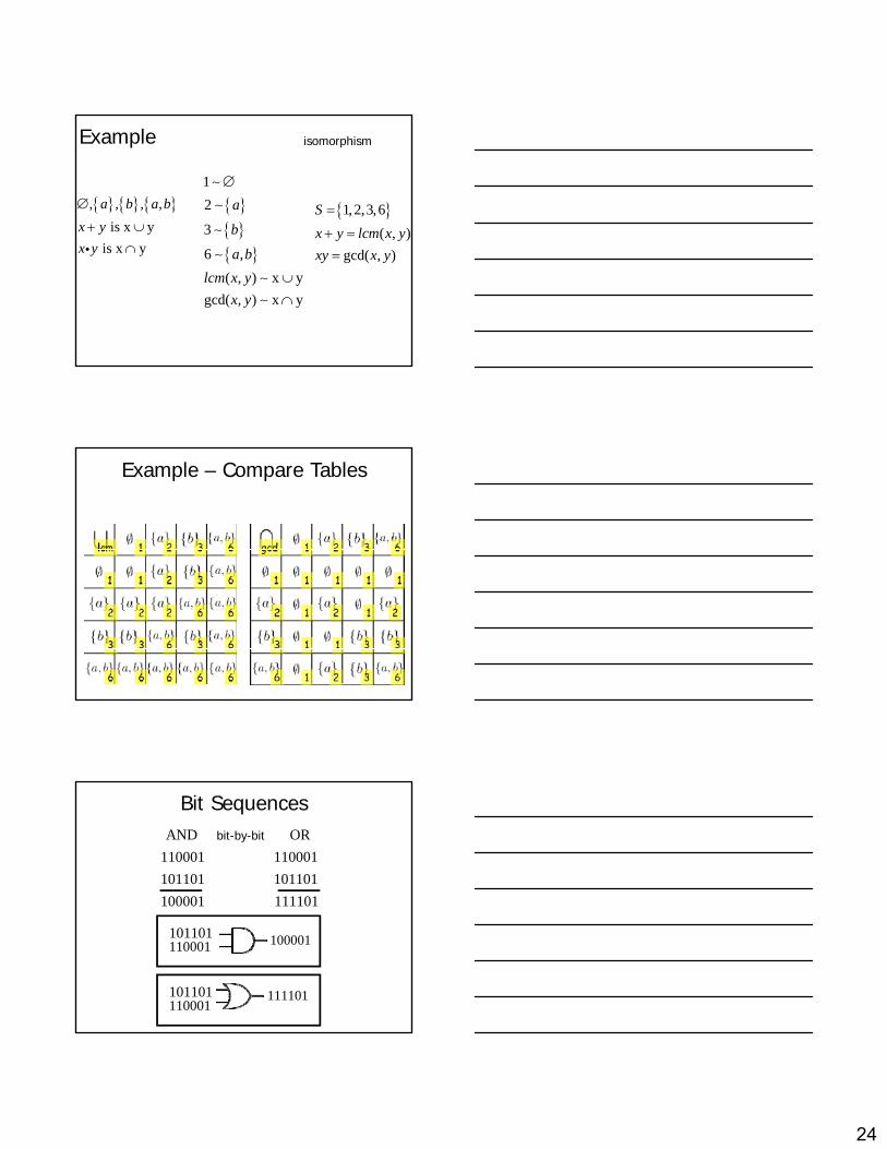
Example
{ }1,2,3,6( , )
Sx y lcm x y=
+ =
{ } { } { }, , , , is x y
a b a bx y∅
+ ∪{ }{ }
12
3
a
b
∅∼∼
∼
isomorphism
( )gcd( , )
y yxy x y= is x yx y ∩i { }6 ,
( , ) x ygcd( , ) x y
a blcm x y
x y∪∩
∼∼∼
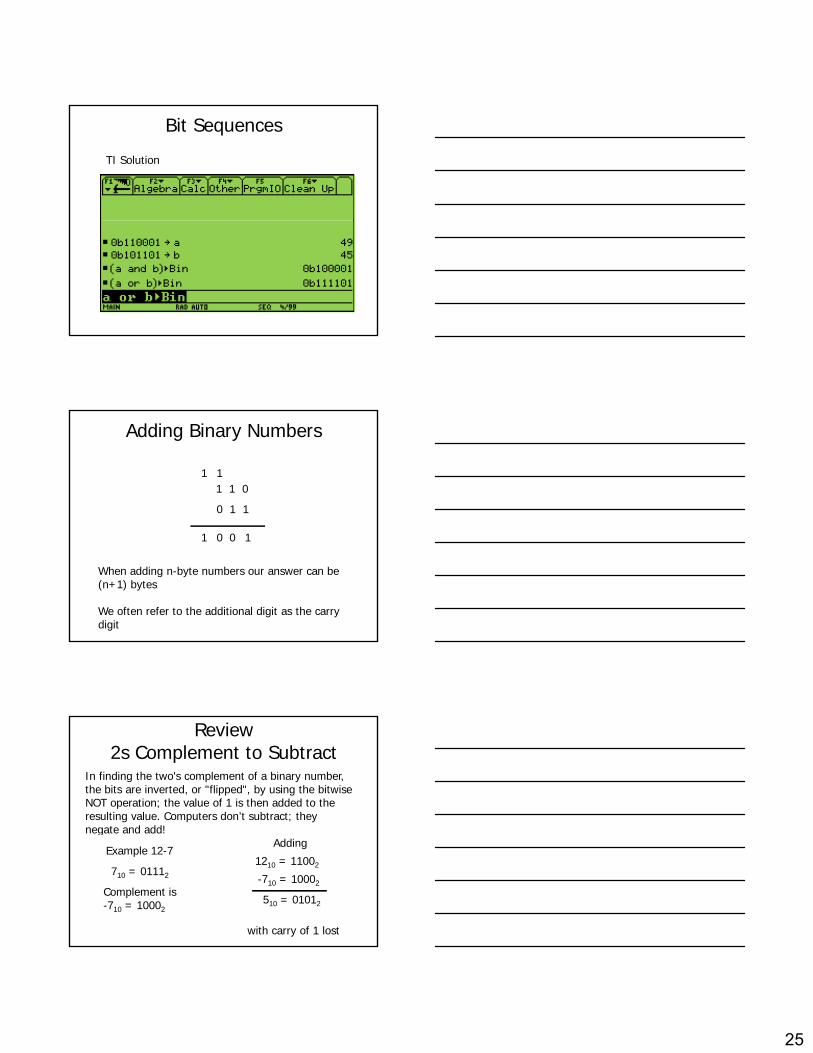
Example – Compare Tables
Bit Sequences AND OR110001 110001101101 101101100001 111101
bit-by-bit
110001 101101 100001
110001 101101 111101
25
Bit Sequences
TI Solution
Adding Binary Numbers
1 1 0
0 1 1
11
1001
When adding n-byte numbers our answer can be (n+1) bytes
We often refer to the additional digit as the carry digit
Review2s Complement to Subtract
In finding the two's complement of a binary number, the bits are inverted, or "flipped", by using the bitwise NOT operation; the value of 1 is then added to the resulting value. Computers don’t subtract; they negate and add!negate and add!
710 = 01112 -710 = 10002
1210 = 11002
510 = 01012
Example 12-7
Complement is-710 = 10002
Adding
with carry of 1 lost
26
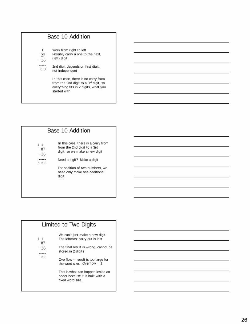
Base 10 Addition
27+36-----
Work from right to leftPossibly carry a one to the next,(left) digit
2nd digit depends on first digit,36
1
g p g ,not independent
In this case, there is no carry fromfrom the 2nd digit to a 3rd digit, so everything fits in 2 digits, what you started with
36
Base 10 Addition
87+36-----
In this case, there is a carry fromfrom the 2nd digit to a 3rddigit, so we make a new digit
Need a digit? Make a digit1 2 3
11
For addition of two numbers, weneed only make one additionaldigit
1 2 3
Limited to Two Digits
We can’t just make a new digit. The leftmost carry out is lost.
The final result is wrong, cannot be stored in 2 digits
87+36-----
2 3
11
Overflow -- result is too large for the word size.
This is what can happen inside an adder because it is built with a fixed word size.
Overflow = 1
2 3
27
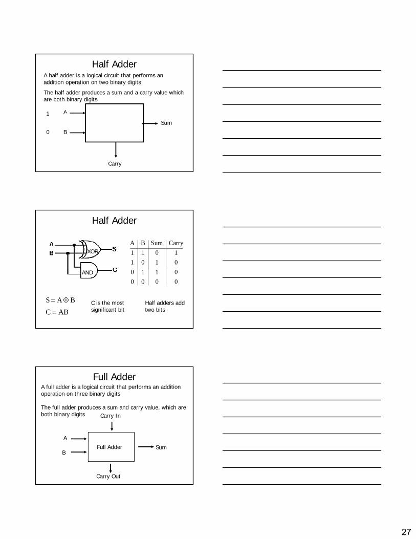
Half Adder
A
A half adder is a logical circuit that performs an addition operation on two binary digits
The half adder produces a sum and a carry value which are both binary digits
1
Half Adder
A
B
Sum
Carry
0
01
1
Half Adder
A B Sum Carry1 1 0 11 0 1 0
XOR
0 1 1 00 0 0 0
C AB=
AND
S A B= ⊕ C is the most significant bit
Half adders add two bits
Full AdderA full adder is a logical circuit that performs an addition operation on three binary digits
The full adder produces a sum and carry value, which are both binary digits Carry In
Full Adder
A
BSum
Carry Out
28
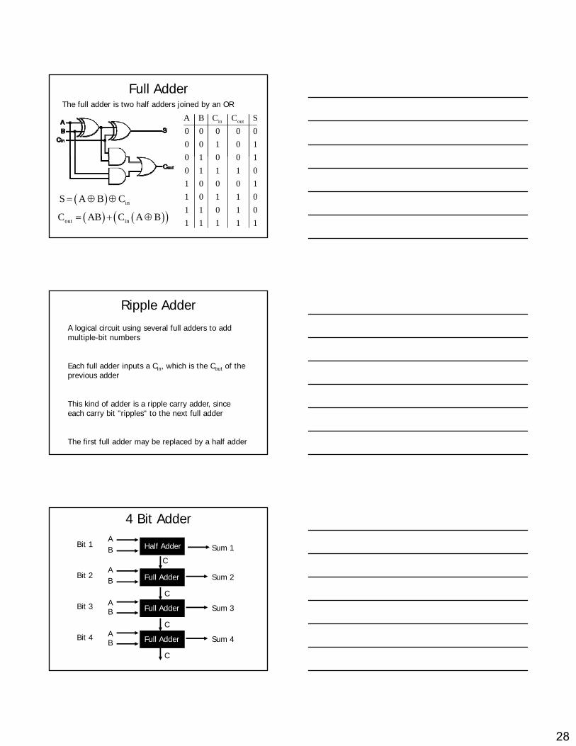
Full AdderThe full adder is two half adders joined by an OR
in outA B C C S0 0 0 0 00 0 1 0 10 1 0 0 1
( ) inS A B C= ⊕ ⊕
( ) ( )( )out inC AB C A B= + ⊕
0 1 0 0 10 1 1 1 01 0 0 0 11 0 1 1 01 1 0 1 01 1 1 1 1
Ripple Adder
A logical circuit using several full adders to add multiple-bit numbers
Each full adder inputs a Cin, which is the Cout of the i ddprevious adder
This kind of adder is a ripple carry adder, since each carry bit "ripples" to the next full adder
The first full adder may be replaced by a half adder
4 Bit Adder
Half AdderAB Sum 1
C
Full AdderAB
Bit 1
Bit 2 Sum 2
C
Full AdderBBit 3
C
ASum 3
Full AdderBBit 4
C
ASum 4
29
Remarks
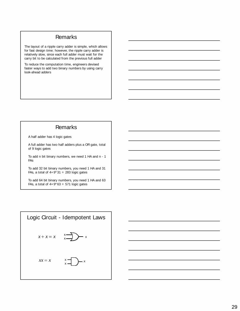
The layout of a ripple carry adder is simple, which allows for fast design time; however, the ripple carry adder is relatively slow, since each full adder must wait for the carry bit to be calculated from the previous full adder
To reduce the computation time, engineers devisedTo reduce the computation time, engineers devised faster ways to add two binary numbers by using carry look-ahead adders
Remarks
A half adder has 4 logic gates
A full adder has two half adders plus a OR gate, total of 9 logic gates
T dd bit bi b d 1 HA d 1To add n bit binary numbers, we need 1 HA and n - 1 FAs
To add 32 bit binary numbers, you need 1 HA and 31 FAs, a total of 4+9*31 = 283 logic gates
To add 64 bit binary numbers, you need 1 HA and 63 FAs, a total of 4+9*63 = 571 logic gates
Logic Circuit - Idempotent Laws
x x x+ = Or xxx
xx x= And xxx
30
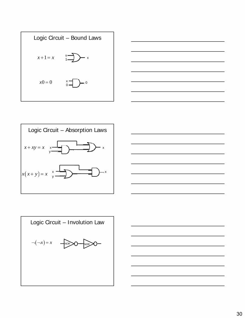
Logic Circuit – Bound Laws
1 x x+ = Or x1x
0 0x = And 0x0
Logic Circuit – Absorption Laws
x xy x+ = xyx
( ) x x y x+ = xxy
Logic Circuit – Involution Law
( ) x x¬ ¬ = NOR NOR
31
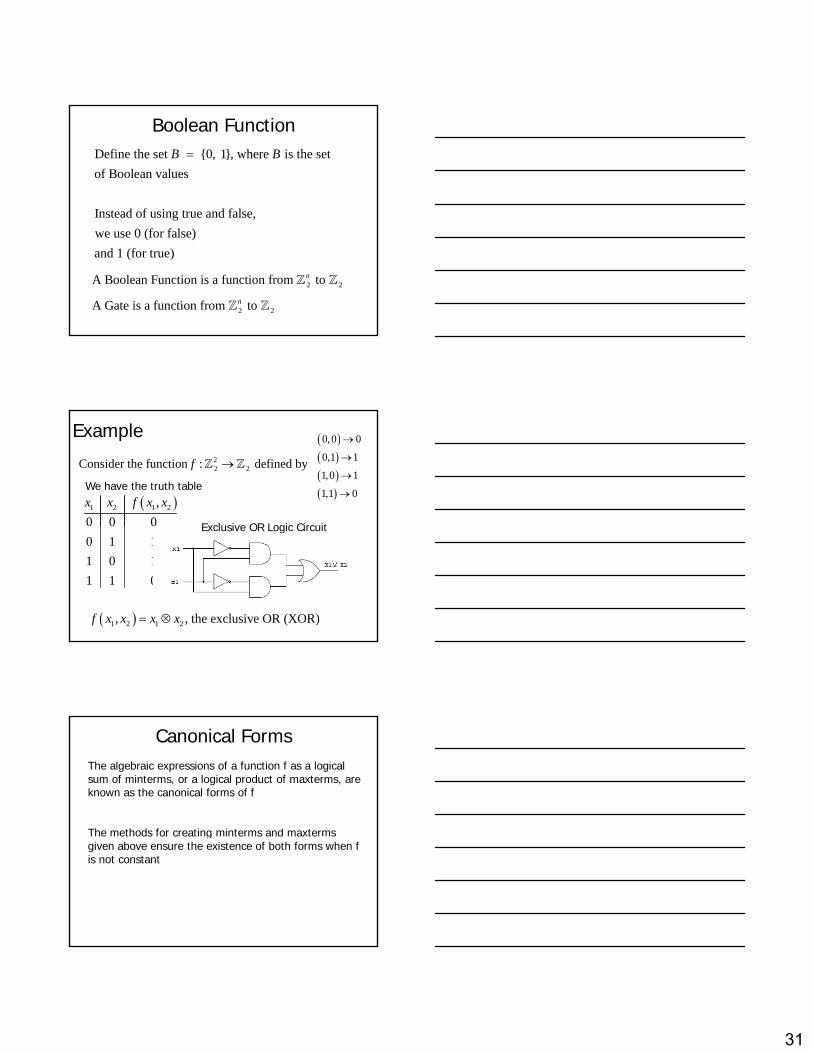
Boolean FunctionDefine the set {0, 1}, where is the set of Boolean values
Instead of using true and false,
B B=
2 2A Boolean Function is a function from to n
we use 0 (for false) and 1 (for true)
2 2A Gate is a function from to n
Example22 2Consider the function : defined byf →
( )( )( )( )
0,0 0
0,1 1
1,0 1
1,1 0
→
→
→
→( )1 2 1 2,0 0 0x x f x xWe have the truth table
Exclusive OR Logic Circuit0 0 00 1 11 0 11 1 0
( )1 2 1 2, , the exclusive OR (XOR)f x x x x= ⊗
Exclusive OR Logic Circuit
Canonical FormsThe algebraic expressions of a function f as a logical sum of minterms, or a logical product of maxterms, are known as the canonical forms of f
The methods for creating minterms and maxtermsThe methods for creating minterms and maxterms given above ensure the existence of both forms when f is not constant
32
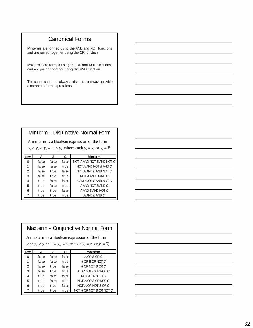
Canonical FormsMinterms are formed using the AND and NOT functions and are joined together using the OR function
Maxterms are formed using the OR and NOT functions and are joined together using the AND functionand are joined together using the AND function
The canonical forms always exist and so always provide a means to form expressions
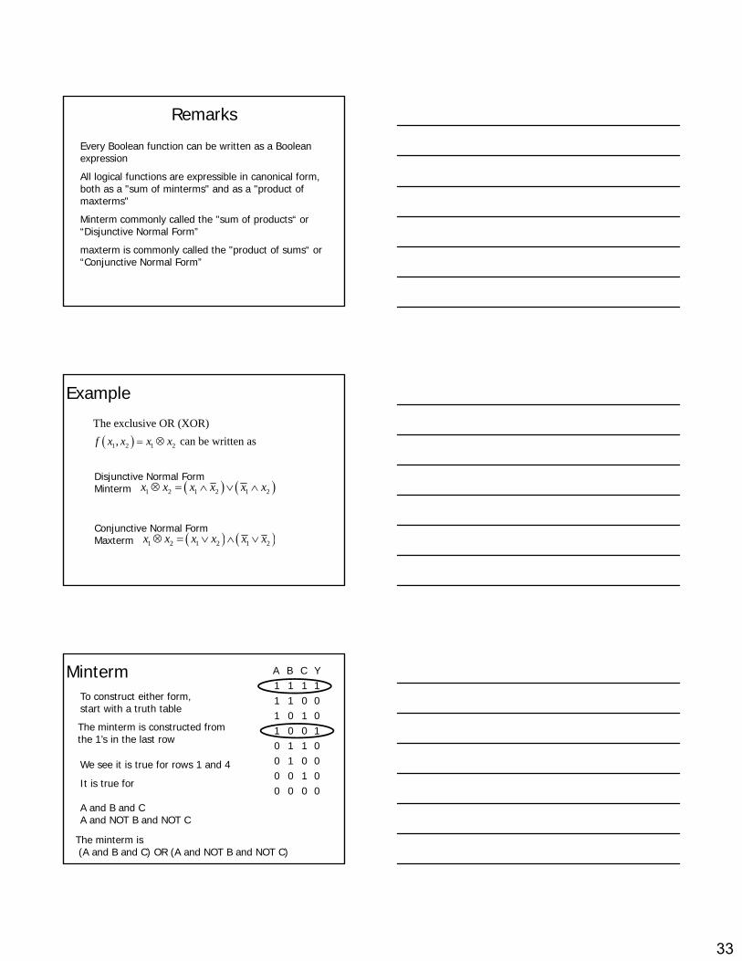
Minterm - Disjunctive Normal Form
row0
A B Cfalse false false
MintermNOT A AND NOT B AND NOT C
1 2 3
A minterm is a Boolean expression of the form where each or n i i i iy y y y y x y x∧ ∧ ∧ ∧ = =
1234567
false false truefalse true falsefalse true truetrue false falsetrue false truetrue true falsetrue true true
NOT A AND NOT B AND CNOT A AND B AND NOT C
NOT A AND B AND CA AND NOT B AND NOT C
A AND NOT B AND CA AND B AND NOT C
A AND B AND C
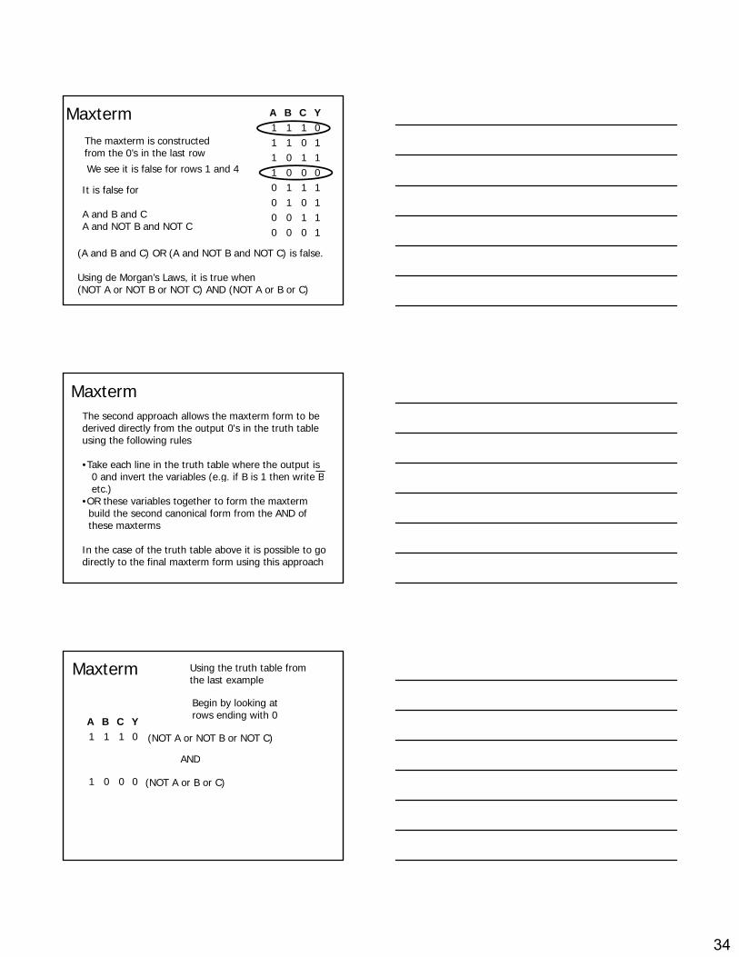
Maxterm - Conjunctive Normal Form
maxtermA OR B OR C
row0
A B Cfalse false false
1 2 3
A maxterm is a Boolean expression of the form where each or n i i i iy y y y y x y x∨ ∨ ∨ ∨ = =
A OR B OR NOT CA OR NOT B OR C
A OR NOT B OR NOT CNOT A OR B OR C
NOT A OR B OR NOT CNOT A OR NOT B OR C
NOT A OR NOT B OR NOT C
1234567
false false truefalse true falsefalse true truetrue false falsetrue false truetrue true falsetrue true true
33
Remarks
Every Boolean function can be written as a Boolean expression
All logical functions are expressible in canonical form, both as a "sum of minterms" and as a "product of maxterms"maxterms
Minterm commonly called the "sum of products“ or “Disjunctive Normal Form”
maxterm is commonly called the "product of sums“ or “Conjunctive Normal Form”
Example
( )1 2 1 2
The exclusive OR (XOR), can be written asf x x x x= ⊗
Disjunctive Normal Form ( ) ( )1 2 1 2 1 2x x x x x x⊗ = ∧ ∨ ∧
jMinterm
( ) ( )1 2 1 2 1 2x x x x x x⊗ = ∨ ∧ ∨Conjunctive Normal Form Maxterm
Minterm A B C Y1 1 1 11 1 0 01 0 1 01 0 0 10 1 1 00 1 0 0
To construct either form, start with a truth table
The minterm is constructed from the 1’s in the last row
0 1 0 00 0 1 00 0 0 0
We see it is true for rows 1 and 4
It is true for
A and B and CA and NOT B and NOT C
The minterm is(A and B and C) OR (A and NOT B and NOT C)
34
Maxterm A B C Y1 1 1 01 1 0 11 0 1 11 0 0 00 1 1 10 1 0 1
The maxterm is constructed from the 0’s in the last row
We see it is false for rows 1 and 4
It is false for0 1 0 10 0 1 10 0 0 1
A and B and CA and NOT B and NOT C
(A and B and C) OR (A and NOT B and NOT C) is false.
Using de Morgan’s Laws, it is true when(NOT A or NOT B or NOT C) AND (NOT A or B or C)
MaxtermThe second approach allows the maxterm form to be derived directly from the output 0's in the truth table using the following rules
•Take each line in the truth table where the output is0 and invert the variables (e g if B is 1 then write B0 and invert the variables (e.g. if B is 1 then write Betc.)
•OR these variables together to form the maxtermbuild the second canonical form from the AND ofthese maxterms
In the case of the truth table above it is possible to go directly to the final maxterm form using this approach
Maxterm
A B C Y1 1 1 01 1 0 1
(NOT A or NOT B or NOT C)
AND
Using the truth table from the last example
Begin by looking at rows ending with 0
1 0 1 11 0 0 00 1 1 10 1 0 10 0 1 10 0 0 1
(NOT A or B or C)
AND
35
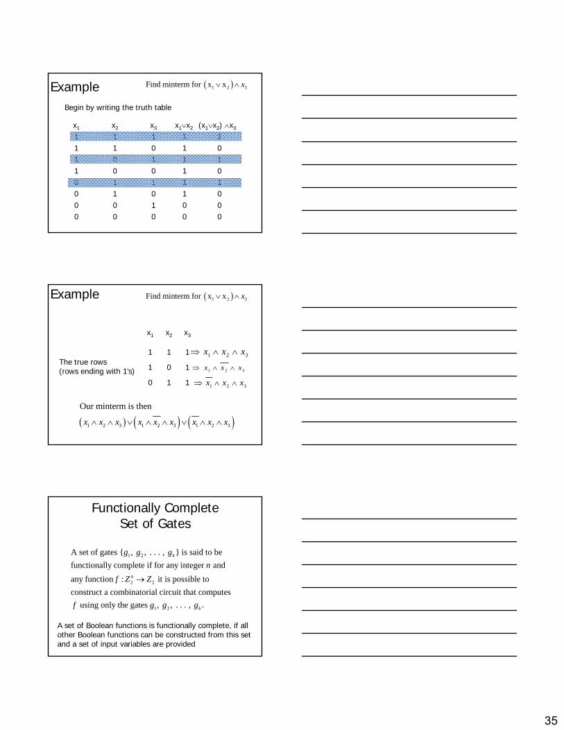
Example ( )1 2 3Find minterm for x x x∨ ∧
x1 x2 x3 x1∨x2 (x1∨x2) ∧x3
1 1 1 1 11 1 0 1 0
Begin by writing the truth table
1 0 1 1 11 0 0 1 00 1 1 1 10 1 0 1 00 0 1 0 00 0 0 0 0
x1 x2 x3
1 1 1
1 0 1The true rows
1 2 3x x x⇒ ∧ ∧
Example ( )1 2 3Find minterm for x x x∨ ∧
1 0 1
0 1 1(rows ending with 1’s)
( ) ( ) ( )1 2 3 1 2 3 1 2 3
Our minterm is then
x x x x x x x x x∧ ∧ ∨ ∧ ∧ ∨ ∧ ∧
1 2 3x x x⇒ ∧ ∧
1 2 3x x x⇒ ∧ ∧
Functionally Complete Set of Gates
1 2A set of gates { , , . . . , } is said to be functionally complete if for any integer and
f i i i ibl
k
n
g g gn
f Z Z
2 2A Gate is a function from to nig
2 2any function : it is possible to construct a combinatorial circuit that computes using only th
nf Z Z
f
→
1 2e gates , , . . . , . kg g g
A set of Boolean functions is functionally complete, if all other Boolean functions can be constructed from this set and a set of input variables are provided
36
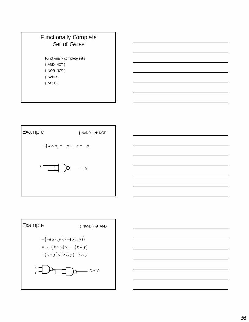
Functionally Complete Set of Gates
Functionally complete sets
{ AND, NOT }
{ NOR, NOT }
{ NAND }
{ NOR }
Example { NAND } NOT
( )x x x x x¬ ∧ = ¬ ∨¬ = ¬
x x¬
Example { NAND } AND
( ) ( )( )( ) ( )
( ) ( )
x y x y
x y x y
x y x y x y
¬ ¬ ∧ ∧¬ ∧
= ¬¬ ∧ ∨¬¬ ∧
= ∧ ∨ ∧ = ∧( ) ( )x y x y x y= ∧ ∨ ∧ = ∧
xy x y∧
37
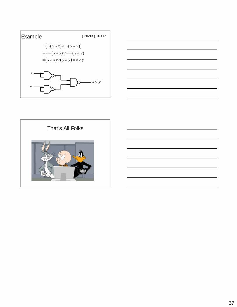
Example { NAND } OR
( ) ( )( )( ) ( )
( ) ( )
x x y y
x x y y
x x y y x y
¬ ¬ ∧ ∧¬ ∧
= ¬¬ ∧ ∨¬¬ ∧
= ∧ ∨ ∧ = ∨
x
yx y∨
That’s All Folks