Embed Size (px)
Citation preview

Bulk Crystal G269
PartB|12.1
12. Bulk Crystal Growth: Methods and Materials
Peter Capper
This chapter covers the field of bulk single crystalsof materials used in electronics and optoelec-tronics. These crystals are used in both activeand passive modes, that is, to produce devicesdirectly in/on bulk-grown slices of material, oras substrates in epitaxial growth, respectively.Single-crystal material usually provides superiorproperties to polycrystalline or amorphous equiv-alents. The various bulk growth techniques areoutlined, together with specific critical features,and examples are given of the types of materi-als, and their current typical sizes, grown by thesetechniques. Materials covered range from group IVs(Si, Ge, SiGe, diamond, SiC), group III–Vs (e.g., suchas GaAs, InP, nitrides, etc.) group II–IVs (e.g., CdTe,ZnSe, HgCdTe (MCT), etc.) through to a wide rangeof oxide/halide/phosphate/borate/tungstate ma-terials. This chapter is to be treated as a snapshotonly; the interested reader is referred to the re-mainder of the chapters in this handbook for morespecific growth and characterization details on thevarious materials outlined in this chapter. Neitherdoes this chapter cover the more fundamentalaspects of the growth of the particular materialscovered; again the reader is referred to relevantchapters within the handbook, or to other sourcesof information in the general literature.
12.1 Background..................................... 269
12.2 History ............................................ 270
12.3 Techniques ...................................... 27112.3.1 Verneuil .......................................... 27112.3.2 Czochralski ...................................... 27112.3.3 Kyropoulos ...................................... 27312.3.4 Stepanov . ........................................ 27312.3.5 Edge-Defined Film Growth................ 27312.3.6 Bridgman . ....................................... 27312.3.7 Vertical Gradient Freeze .................... 27512.3.8 Float Zone ....................................... 27512.3.9 Traveling Heater Method ................... 27512.3.10 Low-Temperature Solution Growth .... 27612.3.11 High-Temperature Solution Growth
(Flux) .............................................. 27612.3.12 Hydrothermal .................................. 27712.3.13 Growth from the Vapor ..................... 27812.3.14 Multicrystalline Si Growth
for Solar Cells ................................... 278
12.4 Materials Grown .............................. 27812.4.1 Group IV .......................................... 27812.4.2 Groups III–V. .................................... 28012.4.3 Groups II–VI. .................................... 28312.4.4 Oxides/Halides/Phosphates/Borates . ... 286
12.5 Conclusions ..................................... 289
References ................................................... 289
12.1 Background
Despite the widespread progress in several epitaxialgrowth techniques for producing electronic and opto-electronic device-quality material, various bulk growthmethods are still used to produce tens of thousandsof tons of such materials each year. These crystalsare used in both active and passive modes; i. e., toproduce devices directly in/on bulk-grown slices ofmaterial, or used as substrates in epitaxial growth,respectively.
This chapter covers the field of bulk single crys-tals of materials used in electronics and optoelectron-ics. Single-crystal material usually provides superior
properties to polycrystalline or amorphous equivalents.The various bulk growth techniques are outlined, to-gether with the specific critical features, and exam-ples are given of the types of materials, and theirtypical current sizes, grown by these techniques. Ma-terials covered range from group IVs (Si, Ge, SiGe,diamond, SiC), group III–Vs (e.g., GaAs, InP, InSb,GaSb, nitrides, etc.) group II–IVs (e.g., CdTe, ZnSe,HgCdTe (MCT), ZnO, etc.) through to a wide range ofoxide/halide/phosphate/borate/tungstatematerials. Thischapter is to be treated as a snapshot only; the interestedreader is referred to the remainder of the chapters in this
© Springer International Publishing AG 2017S. Kasap, P. Capper (Eds.), Springer Handbook of Electronic and Photonic Materials, DOI 10.1007/978-3-319-48933-9_12

PartB|12.2
270 Part B Growth and Characterization
handbook for more specific growth and characterizationdetails on the various materials outlined in this chapter.Many of the crystals grown at a small size mainly forR&D purposes, particularly in Universities, are not dis-cussed, and neither, in general, are organic materials.
Neither does this chapter cover the more fundamentalaspects of the growth of the particular materials cov-ered; again the reader is referred to the relevant chapterswithin this book, or to other sources of information inthe general literature.
12.2 History
Several very useful studies on the history of crystalgrowth in general can be found in the literature [12.1–9]. There were many significant contributions made tothe fundamentals of crystal growth during the 18th and19th centuries, including the development of thermody-namics, undercooling, and supersaturation [12.6, 7]. Interms of crystal growth techniques, it is accepted thatthe first to produce usable crystals on a large scale wasthat of flame fusion by Verneuil [12.10].
Before World War II, synthetic crystals (other thanruby) were mainly used in scientific instruments. How-ever, between 1900 and 1940 there were enormousadvances in both the theoretical aspects and in produc-ing samples for scientific study. The diffusion bound-ary layer was applied by Nernst [12.11], while ideason the growth of perfect crystals were proposed byVolmer [12.12], Kossel [12.13], and Stranski [12.14].Also during this period many of the growth techniquesnow used were also initially developed. The flame fu-sion of Verneuil [12.10] was followed by hydrothermalgrowth [12.15, 16], crystal pulling [12.17], Kyropou-los [12.18], Bridgman growth [12.19–22], and verticalgradient freeze (VGF) [12.23].
During World War II, synthetic crystals were usedas piezoelectric transducers (in sonar) as resonant de-vices (in radar) and as infrared detectors. However,it was the invention of the transistor (announced in1948) that heralded the modern era of crystal growthfor practical purposes rather than for pure scientific in-terest. Teal and Little developed crystal pulling of Ge in1950 [12.24] and Dash [12.25] improved this with the
5% Optical crystals
10 % Acoustic opticscrystals
10 % Laser &nonlinearcrystals
12 % Jewelry& watch industry
60%Semiconductors
3% Scintillationcrystals
Fig. 12.1 Estimated share of the world production of20 000 t of bulk crystals. (After [12.1], copyright ElsevierScience, used with permission)
necking technique to produce dislocation-free material.A key aspect at this stage was that of impurity levels andmeans to measure them. The semiconductors that wereused for such solid-state devices as transistors workbecause they have desired dopants incorporated selec-tively in them. Techniques were developed at this timeto improve the purity of materials, for example, zonerefining [12.26] and float-zone (FZ) refining [12.27,28]. Theoretical aspects developed in this period in-clude the role of screw dislocations in growth [12.29]and the generalized theory of Burton et al. [12.30]. Re-ducing melt inclusions in crystals was discussed byIvantsov [12.31, 32] in terms of diffusional undercool-ing, and by Tiller et al. [12.33] in terms of constitutionalsupercooling. Similar work was carried out in solutiongrowth by Carlson [12.34], who studied flow effectsacross crystal faces, and Scheel and Elwell [12.35], whoderived the maximum stable growth rate and optimizedsupersaturation to produce inclusion-free crystals. Seg-
Table 12.1 Estimated worldwide annual production ratesof crystals (as at 1986, [12.5]). Some materials are mainlyused for non-(electronic/optoelectronic) purposes, for ex-ample, cubic zirconia and much of the ruby are used injewelry, watches, etc. (Items in brackets are small in vol-ume but high in value)
Crystal Rate(t=yr)
Growth methods
Silicon 4000 Czochralski, float-zone,(vapor phase epitaxy VPE)
Metals 4000 Bridgman, Strain annealQuartz 800 HydrothermalIII–V compounds 600 Czochralski, Bridgman (VPE,
liquid phase epitaxy LPE)Alkali halides 500 Bridgman, KyropoulosRuby 500 VerneuilGermanium 400 Czochralski, BridgmanGarnets 200 CzochralskiLithium niobate 100 CzochralskiPhosphates 50 Low-temperature solutionLithium tantalate 20 CzochralskiCubic zirconia 15 Skull meltingTGS 10 Low-temperature solutionDiamond 10 High-temperature solutionII–VI compounds 5 Vapor, Bridgman

Bulk Crystal Growth: Methods and Materials 12.3 Techniques 271Part
B|12.3
regation effects, which are related to mass and heattransfer, were studied by Burton et al. [12.36] for meltgrowth and by van Erk [12.37] for solution growth,while experimental conditions to produce striation-freematerial were established by Rytz and Scheel [12.38].Forced convection in diffusion-limited growth was rec-ognized as being beneficial for open systems withstirrers [12.39–42], while stirring in sealed containerswas accomplished using the accelerated crucible rota-tion technique [12.43].
In 1986, Brice [12.5] estimated the annual produc-tion rates of crystals and Table 12.1 reproduces thatdata. Semiconductor materials clearly dominated at thatstage, in particular silicon and III–V compounds. Later,
Scheel [12.6] gave estimates of 5000 t in 1979, 11 000 tin 1986 (from [12.5]) and approximately 20 000 t in1999 (Fig. 12.1), with a similar total quoted by Scheel in2008 [12.8]. By 1999, the balance had shifted somewhatfrom the earlier estimates, but semiconductors contin-ued to dominate, at � 60%. There were roughly equalpercentages of scintillator, optical, and acousto-opticalcrystals, at around 10�12%. The remainder was madeup of laser and nonlinear optical crystals and crystalsfor jewelry and the watch industries.
A recent book edited by Capper [12.44] givesa comprehensive update on the bulk growth of manyof the materials used in the electronic, optical and opto-electronic fields.
12.3 Techniques
12.3.1 Verneuil
This is the fastest growth method and was the first tobe capable of controlling nucleation and thus produc-ing large crystals of high melting point oxide crystals,for example, sapphire and ruby. Currently, a largenumber of high melting point materials have beengrown by this technique, including ZrO2 (2700 ıC),SrO (2420 ıC), Y2O3 (2420 ıC), etc., but the largestuse is still Al2O3 (often doped to produce ruby, sap-phire, etc.). Figure 12.2 shows a schematic of theequipment used. Many different heat sources havebeen used, for example, solar furnace, glow discharge,plasma torch, arc image and radio frequency heating,but the original gas-flame technique is still the mostpopular. An oxy-hydrogen flame heats the seed crystalplaced on a ceramic pedestal. Powder from a hop-per is shaken through the flame and melts, forminga melt surface on the seed. During growth the seedis lowered, controlling the linear growth rate, whilethe volume growth rate is governed by the powderfeed rate. The balance of these two rates controlsthe crystal diameter and the crystal is normally ro-tated slowly. Ruby crystals up to 200mm diametercan be grown. Drawbacks of the technique includehigh dislocation densities and concentration varia-tions.
12.3.2 Czochralski
Czochralski is a fast growth method and is widely usedfor both semiconductors and oxide/fluoride materialsfor optical applications. It also normally produces themost nearly perfect and homogeneous crystals. How-ever, it is only really applicable to those materials thatmelt congruently or nearly congruently, that is, the solid
and the melt compositions are the same at equilibrium.Normally a crucible material is needed that is compati-ble with the melt, however, the most common cruciblematerial used for silicon, that is, silica, dissolves slowlyin the melt and this raises certain process issues in thegrowth of this material. Capital costs for Czochralskipulling are higher than most other techniques, but it isused when the greatest perfection of grown material isrequired.
Vibrator
Hopper
Sieve
Tricone burner
Ceramic Flame
Liquid film
Crystal
Seed
H2
O2
Fig. 12.2 Schematic of Verneuil growth equipment. (Af-ter [12.5])

PartB|12.3
272 Part B Growth and Characterization
Graphiteheater
Silicacrucible
Melt
Power lead
Laser beam
Fig. 12.3 Schematic of Czochralski growth equipment.(After [12.5])
The largest use is clearly for silicon, but proba-bly � 100 materials are commercially grown using thismethod, while many more are at the research stage.As the diameter of the crystal increases, in silicon forexample from 200 to 300mm, dislocation control be-comes more difficult due to larger radial temperaturegradients. Figure 12.3 shows a schematic of a Czochral-ski growth equipment. The basic method is relativelysimple: The solid charge is placed in the crucible andheated to a temperature several degrees above the melt-ing point. The seed crystal, rotating slowly, is loweredto contact the melt and the seed then slowly melts. Aftera short delay (a few minutes) pulling is commenced andnew material (with slightly reduced diameter) begins togrow. A long narrow neck region is grown to reducedislocations, then the melt temperature is reduced toincrease the diameter. When the crystal attains full di-ameter growth is maintained until the desired length ofcrystal has grown, and growth is terminated by sharplyincreasing the pull rate or increasing the melt tempera-ture so that the diameter reduces to zero.
A constant diameter is maintained by adjusting thepower input to the melt. This is done automatically ei-ther by directly monitoring the diameter optically, thatis, by observing the bright ring around the crystal pe-riphery, or by indirectly measuring the diameter viaweighing methods. Crucibles are normally round basedfor semiconductors but should be relatively flat for ox-ide/halide growth, that is, ionic materials.
Hurle [12.45] discusses the effects, in detail, ofconvection, flows in melts, heat transport, mass trans-port, solute segregation, use of magnetic fields, systemsdynamics and automatic diameter control, morpholog-ical stability, and defect control. In general, as meltsizes have increased natural convective flows have in-creased, leading to turbulence, which causes growthrate fluctuations leading to dopant concentration vari-ations (so-called striations).
For growth of III–V compounds, liquid encapsulatedCzochralski (LEC) was pioneered byMullin [12.46] forGaAs and GaP. Suppression of the volatility of As andP was crucial to the successful growth of these types ofcompounds. This technique involves the use of an in-ert layer of a transparent liquid, usually B2O3, whichfloats on the melt surface and acts as a liquid seal. Mostimportantly, the encapsulant should wet both the cru-cible and crystal so that a thin film adheres to the crys-tal as growth proceeds. The latter prevents dissociationof the hot crystal. Pyrolytic boron nitride (PBN) cru-cibles are now often used and either resistance or r.f.heating is employed. Semi-insulating GaAs is producedin a high-pressure puller (100�200 atm). The main ad-vantage here is that elemental Ga and As can be usedas the starting materials. Diameter is often control bycrystal-weight measurements, rather than meniscus ob-servation. Pull rates are typically < 1 cm=h. Axial ortransverse magnetic fields can again be used to controlmelt turbulence and dopant segregation.
Precious metal (Pt, Ir) crucibles are used for ox-ide crystal growth as high temperatures are used. Toprevent reduction of oxide melts, a partial pressure ofoxygen is needed. Normally, the crucible is not rotatedor translated and the growth rate is greater than thepulling rate as the melt height decreases. Growth ratesare a few mm=h, at best, so growth times are normally> 1 week. Large temperature gradients can lead to meltturbulence, which in turn produces a banded structureof solute concentration and varying stoichiometry inthe crystals. Control of convection in these systemsis therefore of critical importance. Rudolph and Kaki-moto [12.47] have outlined various means of controllinguniformity and stability of crystal growth from the meltby complementing internal parameters (e.g., tempera-ture field, pressure, growth velocity, etc.) by externalinfluences, for example, mechanical, electrical, and me-chanical fields. Stirring during crystal growth can oftenbe essential to enhance solute transport through thegrowth fluid, to homogenize the solute concentration inthe fluid and solid, and to reduce the thickness of thesolute diffusion boundary layer (in order to prevent con-stitutional supercooling and hence the morphologicalinstability of the crystal). The question that obviouslyarises then is why are the properties of the crystal not
Bulk Crystal Growth: Methods and Materials 12.3 Techniques 273Part
B|12.3
markedly affected by the periodic disturbances appliedto growth fluids? The answer lies in a comparison ofthe time scales involved. Movement of solute speciesin melt growth is normally of the order of hundreds ofcm=s. With growth rates in the region of 10�2 cm=s,and induced fluctuations in the region of cm=s solutemovement dominates. In addition, if the characteristicratio of D=ı2 (with D the diffusion coefficient and ı theboundary layer thickness) is less than the frequency ofany hydrodynamic changes and their related tempera-ture oscillations then mass diffusivity cannot follow thethermal changes.
12.3.3 Kyropoulos
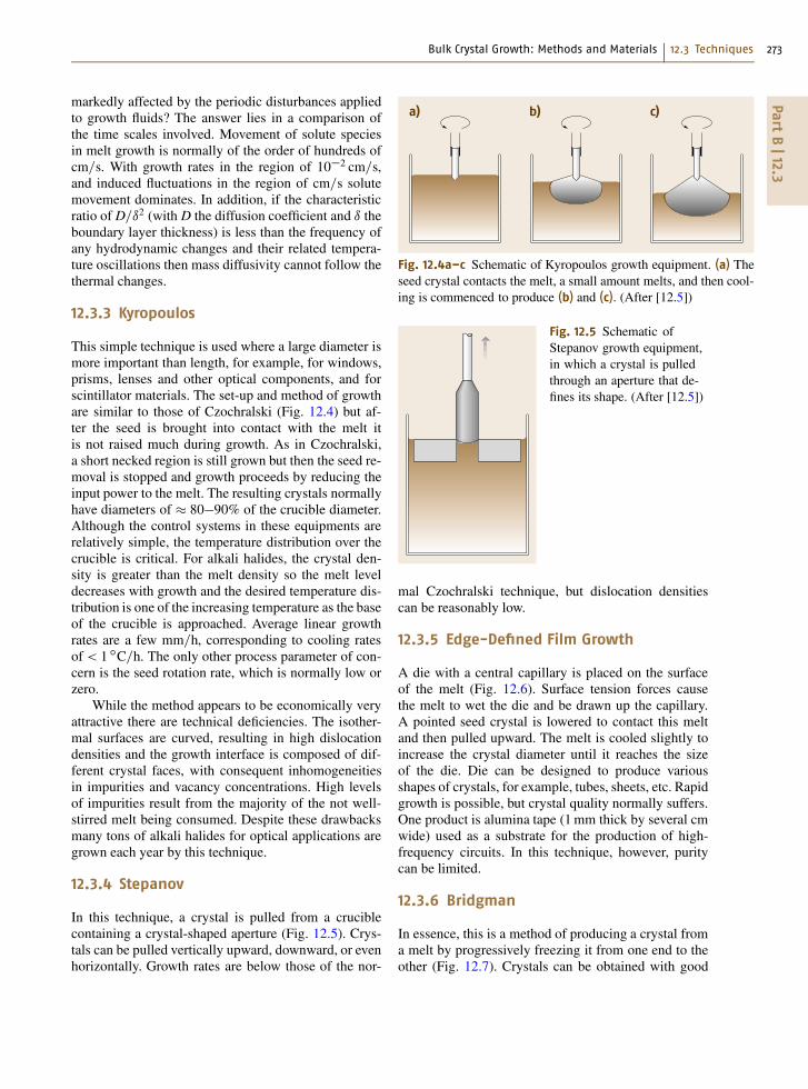
This simple technique is used where a large diameter ismore important than length, for example, for windows,prisms, lenses and other optical components, and forscintillator materials. The set-up and method of growthare similar to those of Czochralski (Fig. 12.4) but af-ter the seed is brought into contact with the melt itis not raised much during growth. As in Czochralski,a short necked region is still grown but then the seed re-moval is stopped and growth proceeds by reducing theinput power to the melt. The resulting crystals normallyhave diameters of � 80�90% of the crucible diameter.Although the control systems in these equipments arerelatively simple, the temperature distribution over thecrucible is critical. For alkali halides, the crystal den-sity is greater than the melt density so the melt leveldecreases with growth and the desired temperature dis-tribution is one of the increasing temperature as the baseof the crucible is approached. Average linear growthrates are a few mm=h, corresponding to cooling ratesof < 1 ıC=h. The only other process parameter of con-cern is the seed rotation rate, which is normally low orzero.
While the method appears to be economically veryattractive there are technical deficiencies. The isother-mal surfaces are curved, resulting in high dislocationdensities and the growth interface is composed of dif-ferent crystal faces, with consequent inhomogeneitiesin impurities and vacancy concentrations. High levelsof impurities result from the majority of the not well-stirred melt being consumed. Despite these drawbacksmany tons of alkali halides for optical applications aregrown each year by this technique.
12.3.4 Stepanov
In this technique, a crystal is pulled from a cruciblecontaining a crystal-shaped aperture (Fig. 12.5). Crys-tals can be pulled vertically upward, downward, or evenhorizontally. Growth rates are below those of the nor-
a) b) c)
Fig. 12.4a–c Schematic of Kyropoulos growth equipment. (a) Theseed crystal contacts the melt, a small amount melts, and then cool-ing is commenced to produce (b) and (c). (After [12.5])
Fig. 12.5 Schematic ofStepanov growth equipment,in which a crystal is pulledthrough an aperture that de-fines its shape. (After [12.5])
mal Czochralski technique, but dislocation densitiescan be reasonably low.
12.3.5 Edge-Defined Film Growth
A die with a central capillary is placed on the surfaceof the melt (Fig. 12.6). Surface tension forces causethe melt to wet the die and be drawn up the capillary.A pointed seed crystal is lowered to contact this meltand then pulled upward. The melt is cooled slightly toincrease the crystal diameter until it reaches the sizeof the die. Die can be designed to produce variousshapes of crystals, for example, tubes, sheets, etc. Rapidgrowth is possible, but crystal quality normally suffers.One product is alumina tape (1mm thick by several cmwide) used as a substrate for the production of high-frequency circuits. In this technique, however, puritycan be limited.
12.3.6 Bridgman
In essence, this is a method of producing a crystal froma melt by progressively freezing it from one end to theother (Fig. 12.7). Crystals can be obtained with good

PartB|12.3
274 Part B Growth and Characterization
a) b) c)
Fig. 12.6a–c Schematic of edge-defined film growth equipment.(a) The melt wets the die and is drawn up the capillary; (b) theseed is contacted to the melt and pulled up and cooling starts toincrease the crystal size; (c) the crystal reaches the size of the die.(After [12.5])
dimensional control and the method uses relatively sim-ple technology requiring little supervision. However, asthe diameter increases, controlling heat flow becomesprogressively more difficult. A wide range of materi-als have been produced by this technique, includingsapphire at a melting point of � 2370 ıC. One majorrequirement is that neither the melt nor its vapor mustattack the crucible material significantly. Dislocationdensities can also be limited to > 104 cm�2, and manymaterials contain low-angle grain boundaries.
Growth rates can be in the range 0:1�30mmh�1.Either the crucible or the furnace can be moved toachieve movement of the freezing isotherm, and bothvertical and horizontal orientations are used. Cruciblematerials include silica (for covalently bonded crys-tals), graphite, and some metals (e.g., Mo for sapphiregrowth). Traditionally, crucibles have tapered tips to tryto restrict nucleation to one crystal, although seed crys-tals can also be used. If spurious nucleation occurs itusually forms at the crucible walls, but this can be sup-pressed by making the growth face concave into themelt. Baffles are often used to separate upper and lowerparts of the furnace to ensure thermal isolation. A lowradial temperature gradient is needed to reduce disloca-tion densities. Calculating the temperature distributionis possible [12.48]. The most obvious requirements area large temperature gradient at the growth interface andlow-temperature gradients in the radial direction.
Impurity distributions in crystals are, in general,governed by the type of mixing in the melt. In stirredmelts, so-called normal freezing, the relevant equationis
Cs D keffC0.1� x/keff � 1 ;
where Cs is the concentration in the solid, C0 the initialconcentration, keff is the effective distribution coeffi-cient, and x is the fraction solidified. In unstirred melts,
PulleyDrum
Lid
Upperwinding
Melt
Baffle
Crystal
Lowerwinding
T/C
T/C
Fig. 12.7 Schematic of Bridgman growth equipment. (Af-ter [12.5])
the interface segregation coefficient k� governs the seg-regation behavior
Cs D k�C0
�1� .1� k�/
k
��1� exp
�� .1� k�/k�fz
DL
�;
where f is the growth rate, z the axial distance, and DL
is the diffusion coefficient. For a molten zone of lengthL, the equation is
Cs D C0Œ1C .keff � 1/ exp.�keff x/� :
For materials with a volatile component, there are sev-eral possible refinements of the basic process, for exam-ple, sealed ampoules, overpressure, and liquid encapsu-lation (e.g., using B2O3). Normally in sealed-ampoulegrowth there is a lack of control over stirring. For verti-cal systems, the accelerated crucible rotation technique(ACRT) can be used, and this author has developed thisrefinement for the growth of mercury cadmium telluride(MCT) up to 70mm in diameter [12.49]. Faster stablegrowth rates are possible with ACRT [12.50], as arelarger diameter crystals, improved uniformity and bet-ter crystallinity.

Bulk Crystal Growth: Methods and Materials 12.3 Techniques 275Part
B|12.3
Silica tube
Feed rod
Zone
R. F. Coil
Crystal
Seed
Fig. 12.8Schematic offloat-zone growthequipment.(After [12.5])
Zharikov [12.9, Chap. 3] discussed how axial vi-brational control can be used to control the heat andmass transfer and growth kinetics during growth fromliquids. Low-frequency, small-amplitude vibrations al-low growth of high-quality crystals at high growth rates,and also provide control of stoichiometry and dopantdistribution. This technique suppresses temperature os-cillations at the interface and improves radial and axialdistributions of impurities. It can also be used for non-electroconducting melts and liquids with high Prandtlnumbers. Applications range from semiconductors todielectrics produced from Bridgman, TSSG, Czochral-ski, and float-zone techniques.
12.3.7 Vertical Gradient Freeze
The vertical gradient freeze (VGF) technique involvesthe progressive freezing of the lower end of a meltupward. This freezing process can be controlled bymoving the furnace past the melt or, preferable, bymoving the temperature gradient in a furnace with sev-eral independently controlled zones. Low-temperaturegradients are normally obtained, leading to reduced dis-location densities, and the crystal is of a defined shapeand size. Difficulties include furnace design, the choiceof boat material, and the issue of seeding.
The majority of melt-grown crystals are producedby the Bridgman and Czochralski techniques (and theirvariants). In general, if no suitable crucible can befound then other methods are required, for example,Verneuil.
Quartz
Sourcematerial
Stationary heater
Temp.T–ΔT T+ΔT
CdxHg1–xTe
Fig. 12.9 Schematic of THM growth equipment. (Af-ter [12.5])
12.3.8 Float Zone
In this technique, a molten zone is maintained betweentwo solid rods (Fig. 12.8). By moving the zone relativeto the rods, one of them grows, and a single crystal canbe grown if a seed is used. Silicon is the only mate-rial grown on a large scale by this technique. The onlyother use for it is in the small-scale growth of very purecrystals, as no crucible contact is involved. For silicon,r.f. heating is used, with frequencies of 2�3MHz fordiameters > 70mm. There is a steep temperature gradi-ent that induces flows in the molten zone, and if boththe seed and feed rods are rotated then the shape ofthe solid/liquid interface can be controlled. The moltenzone normally moves upward.
12.3.9 Traveling Heater Method
The traveling heater method (THM) technique wasdeveloped for II–VI alloy growth (Te-based) by Tri-boulet [12.51]. In this technique, a molten zone is madeto migrate through a homogeneous solid source mate-rial. This is normally accomplished by slowly movingthe ampoule relative to the heater (Fig. 12.9). The keyrequirement here is to obtain the appropriate tempera-ture profile, also shown in Fig. 12.9. Matter transportis by convection and diffusion across the solvent zoneunder the influence of the temperature gradient result-ing from the movement. For alloy growth, a steadystate can be reached where the solvent dissolves a solidof composition C0 at the upper growth interface anddeposits, at near-equilibrium conditions, a material ofthe same composition at the lower growth interface.Growth occurs at a constant temperature below thesolidus temperature and hence shows all the advantages

PartB|12.3
276 Part B Growth and Characterization
WaterSeed Water to
thermostat
Stirrer(1 of 3)
Solution
Polystyrene
Aluminum
Cork
Crystal
Fig. 12.10 Schematic of low-temperature solution growthequipment. (After [12.5])
of low-temperature growth. When tellurium was usedas a molten zone there was a marked purification effect.Seeding was also found to be possible with the tech-nique, as was growth of larger diameter material thanwith the other common melt techniques used for thesecompounds.
Problems with THM include the availability of suit-able feed material with the required composition anddimensions, although several different routes have beenused to overcome this problem. Natural convection isthe dominant mechanism of material transport, whichled to the addition of ACRT to the basic THM methodfor some of the ternary alloys.
By producing two bevelled cylinders of binary com-pounds graded-composition alloys were also produced.These were then used to assess the effects of com-position on various electrical and optical propertiesin the given system. Other modifications to the ba-sic process included the cold THM process, in whichthe relevant metallic elements were used as the sourcematerial. This produced a process that accomplishedsynthesis, growth, and purification at low temperatureall in a single run. To avoid the problems resultingfrom solvent excess in the crystal sublimation THMwas developed in which an empty space of the samedimension as the molten zone is used. This methodwas successfully applied to the growth of ZnSe. Toimprove the purification effect, repeated runs on thesame material were used. A drawback of this is oneof repeated handling, which in turn was solved byusing the multipass THM technique, which can be
thought of as a variety of the classical zone-meltingmethod.
12.3.10 Low-TemperatureSolution Growth
Most of the crystals grown by this technique are wa-ter soluble. This limits their use to applications inwhich moisture can be excluded. Growth rates arelow (0:1�10mm=d), as the growth faces are unsta-ble. This is due to the concentration gradient near thegrowth face, in addition to which the crystal is nor-mally totally immersed in the solution so that latent heatevolution increases the adverse supersaturation gradient(Fig. 12.10).
Water (both light and heavy) is used in � 95% ofthe cases, and must be highly pure. All equipment mustbe carefully cleaned and protected from dust and thesolutions must be stirred vigorously while being pre-pared. Both slow cooling and solvent evaporation tech-niques are used. Large volumes of solution (> 100 l)are needed for very large crystals of, e.g., KH2PO4
(KDP). These large volumes imply very long thermaltime constants, which can be increased by adding ther-mal insulation, up to a limit. Large time constants makeit easy to obtain good temperature control. The growthequipment is normally held in temperature-controlledrooms. Although temperature stability is key, other pa-rameters, such as fluctuations in stirring, can lead tolarge changes in growth rate too.
Solvent evaporation simplifies the temperature con-trol system and makes it more reliable. However, it isdifficult to ensure a constant acceptable rate of lossof solvent. This can be approached by using a water-cooled condensation region. One drawback of this tech-nique is that concentrations of impurities increase as thegrowth proceeds.
12.3.11 High-TemperatureSolution Growth (Flux)
This method is used for those materials that melt incon-gruently; the solvent (flux) reduces the freezing pointbelow the relevant temperature to produce the desiredphase of the compound. Both liquid metals (Ga, In, Sn)used in semiconductors and oxides/halides (e.g., PbO,PbF2) used for ionic materials are employed as solvents.Often, an excess of one of the components will be used(e.g., Ga for GaAs and GaP for instance) or a commonionic material (e.g., K2CO3 for KTaxNb1�xO3). Alter-natively, the solvents contain large atoms, such as Pband Bi, which are too large to enter the lattice of the de-sired crystal. Mixed solvents, for example, alkali metalions, break the chains that exist in B2O3, SiO2, and

Bulk Crystal Growth: Methods and Materials 12.3 Techniques 277Part
B|12.3
Crystals
Frame
Baffle
Nutrientchipsin basket
Heater
Fig. 12.11 Schematic of hydrothermal growth equipment.(After [12.5])
Bi2O3, lowering viscosities and surface tensions. Thebook by Elwell and Scheel [12.4] contains much usefulinformation in this field.
Slow cooling of high-temperature solutions wasused between 1950 and 1970 to produce hundredsof different materials. Small crystals were normallyobtained but these were sufficient to obtain usefulmeasurements of magnetic, optical, and dielectric prop-erties. Later, seeded growth and stirring using ACRTled to much larger crystals. A Czochralski-type pullingtechnique can also be used in high-temperature solutiongrowth to produce larger crystals.
12.3.12 Hydrothermal
This is growth from aqueous solution at high temper-ature and pressure. Most materials grown have lowsolubilities in pure water, so other materials (calledmineralizers, for example, NaOH and Na2CO3) areadded to increase the solubility. Quartz is the onlymaterial grown on a significant scale by this method,although ZnO is also produced commercially by thistechnique.
Natural quartz crystals are used as seeds, as theyhave lower dislocation densities. Growth proceeds inthe temperature-gradient transfer mode. Nutrient is heldin the lower part of the liquid in an autoclave. This re-gion is held at between 5 and 50 ıC above the upperportion of the autoclave. Convection carries the hot su-
a)
b)
SeedCrystal
Nutrient
Containing tubePlugFurnace
ChargeAmpoule Crystal
Distance
Temperature
Temperature
T1
T2
Fig. 12.12a,b Schematic of vapor growth equipment.(a) Seeded growth; (b) Piper–Polich set-up. (After [12.5])
persaturated liquid to the cooler upper regions, wheredeposition occurs on the seed crystals (Fig. 12.11).These autoclaves can be operated at up to 400 ıC and2000 atm pressure for � 10 yr without degradation. Au-toclaves can be up to 1m in diameter and 2:5m highfor low-pressure growth from Na2CO3 solution, while40 cm diameter and 8m high autoclaves are typical forgrowth from NaOH.
Resistive heating elements are strapped to the out-side of the autoclave and connected to two controlsystems, allowing independent control of the temper-atures in the solution and growth zones. Brice [12.5]presents a table that shows some typical hydrothermalgrowth conditions for a wide range of materials.
The essential problem in the growth of quartz isto produce useful devices with reasonable yields withOH concentration (measured by IR absorption) of <100 ppma. Several parameters restrict the maximumgrowth rate to � 0:5mm=d.

PartB|12.4
278 Part B Growth and Characterization
12.3.13 Growth from the Vapor
Vapor growth has some applications, particularly inhigh melting point materials and in II–VI compoundssuch as ZnSe and ZnS (Fig. 12.12). High-temperaturevapor transport, or sublimation, of SiC has progressedrecently to producing 1�2 in crystals. Growth proceedsby sublimation of a SiC source at 2000�2500 ıC innear-vacuum conditions onto a seed held at � 1000 ıClower than the source. 6H-polytype material orientedat h0001i is produced. Growth rates are � 2mm=h.Problems remaining include impurities (� 1016 cm�3),voids, high dislocation densities, and mixed polymor-phism.
12.3.14 Multicrystalline Si Growthfor Solar Cells
Green [12.52] discusses the production of multicrys-talline Si slices for photovoltaic applications and notesthat in 2011 approximately 48% of the world pro-duction was based on this material. Advantages overthe Czochralski process are noted as lower capi-tal costs, higher throughput, and a higher toleranceto poor feedstock quality. Basically, the process in-
Silicon
Mold
a) b)
Fig. 12.13 (a) Direction solidification of silicon withina mold: (b) smaller sections are sawn from the main ingot.(After [12.52])
volves the controlled solidification of molten silicon ina container to give silicon ingots with large columnargrains, normally propagating from the container base(Fig. 12.13a). These rectilinear ingots can be very large,up to 400�600 kg, and they are sawn into smaller moremanageable sections, � 150mm in size (Fig. 12.13b),before being sliced into wafers by continuous wire saw-ing. This material is capable of producing solar cellswith � 90% of the performance of single-crystal Si,but due to the higher packing density possible due tothe square geometry, this difference is masked at themodule level where the overall performance is equiva-lent.
12.4 Materials Grown
This section summarizes the position regarding thewide range of materials used in electronics and opto-electronics. Again the reader is referred to the followingrelevant chapters for more in-depth coverage of a par-ticular material. The section is subdivided roughly intogroup IV, group III–V, group II–VI, oxides, halides, andfinally phosphates/borates.
12.4.1 Group IV
Silicon (Germanium)The growth of silicon still dominates the electronicsindustry in terms of size of activity. Hurle [12.45] de-scribes in detail the growth of silicon by the Czochralskimethod. In essence, a polysilicon charge is placed ina high-purity quartz crucible mounted in pre-bakedgraphite supports. Chains or cables are used in thepulling system, rather than rods, to limit the height ofmodern pullers. Both the crystal and the crucible canbe rotated, although the details of this aspect vary frommanufacturer to manufacturer and are proprietary. Asthe growth proceeds, the crucible is raised to maintainthe position of the melt surface in the heater.
Silicon has two major advantages from a crys-tal growth perspective: a high thermal conductivity
(which permits removal of latent heat of solidification)and a high critical resolved shear stress (which allowshigh thermal gradients without dislocation generation).These two factors enable high growth rates, leading toeconomic benefits. Heat is provided by picket-fence-type graphite heaters. Most commercial pullers arehighly automated with full computer control. In mostcases, diameter control is achieved via monitoring ofthe bright ring around the meniscus of the growingcrystal. Oxygen is a particular problem and is intro-duced via erosion of the silica crucible by the melt.Convection moves the oxygen within the melt towardthe crystal, where it is incorporated. A similar situationarises with carbon monoxide loss from the melt. Prob-lems with convection have increased as the diametersof silicon crystals have increased over the past severaldecades. This convection controls concentrations anddistributions of oxygen, carbon, and other unwanted im-purities.
Although current production of large-diameter ma-terial is at the 300mm level, there have been reports of400mm diameter material [12.53] and even 450mm (�450 kg) [12.8, Chap. 6]. In this case, it was necessaryto grow a secondary neck below the Dash dislocation-reducing one as the thin Dash neck could not hold the

Bulk Crystal Growth: Methods and Materials 12.4 Materials Grown 279Part
B|12.4
weight of the crystal. One report [12.54] shows how co-doping Si with B and Ge can obviate the need for thisnarrow-neck region, while maintaining dislocation-freegrowth. Rudolph and Kakimoto [12.47] report how theuse of a 0:35T magnetic field can reduce turbulence insuch large melts.
The highest grade of silicon i. e., the high-est purity, is probably still produced by the float-zone (FZ) method, rather than the Czochralski tech-nique [12.55, 56]. The higher purity (particularly re-garding carbon and oxygen) and better microde-fect control result in higher solar cell efficien-cies in FZ material. Faster growth rates and heat-ing/cooling times together with the absence of cru-cibles and hot-zone consumables also give FZ mate-rial an economic advantage over Czochralski mate-rial.
Table 12.2 summarizes the present position on sizesof various crystals, including silicon and germaniumand silicon/germanium. The author does not claim thatthis list is complete nor is it authoritative, it merelyserves to show the range of crystals and sizes currentlybeing grown by bulk growth techniques. The informa-tion is taken from a number of published conferenceproceedings [12.57–66] and other sources [12.8, 9, 44,49, 67–69].
Silicon CarbideThe growth of SiC for semiconductor devices, asopposed to abrasive applications, became success-ful when substrates could be reproducibly grown upto large sizes [12.70–72]. Currently, substrates upto 50mm diameter are commercially available and100mm diameter substrates have been reported by Ta-lalaev et al. [12.9, Chap. 2]. The current method is thatof seeded sublimation growth. A water-cooled quartzreactor enclosure surrounds a graphite crucible, whichis heated by r.f. means. Crucible sizes are slightly largerthan the required crystal size and SiC powder (particlesize 20�200�m) and/or sintered polysilicon is used asthe source. Typically a distance of 1�20mm betweenthe seed and the source is used. At the high process tem-peratures of 1800�2400 ıC, volatile species of Si2C,SiC2, and Si evaporate from the source and deposit onthe seed. The source temperature determines the rateof evaporation, and the temperature difference betweenthe source and the seed determines the diffusion trans-port rate; together these two temperatures govern thegrowth rate. The Si W C ratio is a key control parameterfor proper growth of the desired material. Sublimationis normally performed in vacuum or inert gas, suchas argon. The pressure of this gas also controls thegrowth rate to an extent. Growth rates can reach up to0:5�1:0mm=h, and crystal lengths of up to 20�40mm
are achieved. Doping can be accomplished via nitrogenand aluminum addition for n- and p-type material, re-spectively.
Polytype control is obtained by carefully choos-ing the seed orientation, with growth on the (0001) Siface giving 6H material, while 4H material grows onthe (000N1) face. Both growth temperature and pressureand intentional/unintentional impurities can also affectthe polytype obtained. One remaining problem is thatof micropipes within the material. These are hollowcore defects of 1�10�m diameter, although their den-sity has been reduced from 1000 to 1 cm�2 in the bestsamples. Maintaining good control over the nucleationconditions can reduce micropipe density.
DiamondHigh-pressure diamond is produced under condi-tions where it is thermodynamically more stable thangraphite [12.73]. However, very high temperatures andpressures are required for growth, unless catalysts arealso employed. Clearly a detailed knowledge of thediamond–graphite pressure–temperature phase diagramis a prerequisite for successful growth. For example,in static compression, 8�20GPa of pressure and tem-peratures of 1000�3000 ıC are needed. Carbon sourcesinclude graphite, amorphous carbon, glassy carbon, andC60. Dynamic compression techniques employ pres-sures of 7�150GPa. A wide variety of catalysts havebeen used ranging from conventional ones, for exam-ple, transition metals, to carbide-forming elements (Ti,Zr, etc.), to Mg, to oxygen-containing materials (car-bonates, hydroxides, etc.), to inert elements (P, Cu, Zn,etc.) to hydrides.
Crystals above 1mm size are grown by the tempera-ture gradient method. Growth temperature, temperaturegradient, growth time, type of catalyst, and impuritiesall affect the growth. Crystals up to 10�12mm in sizeare commercially available from high-temperature–high-pressure growth, see Sumiya [12.74]. Growth ratescan reach 10mg=h and are governed by the growth tem-perature and the temperature gradient. If a high-qualitydiamond seed is used crystals free of major defects,such as inclusions, stacking faults and dislocations, canbe obtained. Impurities, mainly form the catalysts used,are still an issue, as is their nonuniform distribution.
More recent work on CVD techniques has led to di-amond crystals up to 100mm in diameter and 1�2mmthickness [12.75]. This book also gives details of theuse of diamond in a very wide range of device applica-tions, including radiation/neutron detectors, electronicdevices, for example, field effect transistors (FETs),electrochemical, and biological sensors and microelec-tromechanical devices. It even describes the area ofsuperconductivity in diamond films.

PartB|12.4
280 Part B Growth and Characterization
Table 12.2 Typical sizes (i. e., diameter) of a selection of bulk-grown crystals (in mm and/or weight in kg) currently inproduction and in R&D
Crystal Commercial R&DSilicon (Cz) 300 (250 kg) 450 (450 kg)Silicon (FZ) 100Silicon (multicrystalline) 680� 680mm (400�600 kg)Germanium 75 200�300Silicon/Germanium 35 (120mm long)SiC 50 100Diamond 100 (1�2mm thick) 100GaAs 200 (50 kg) 200InP 150 150GaSb 50 75GaInSb 50InSb 75 100InAs 50InGaAs 10GaInAsSb 30GaN (sublimation) 50AIN (physical vapor transport, PVT) 25 (5mm thick) 40 (core in 50mm slices)MCT 50 70CdZnTe 140 (10 kg) 140 (12 kg)Bi2Te3 12 28ZnSe (vapor, LEC) 60ZnTe 80ZnO 50 75 (10mm thick)HgMnTe 30CdMnTe 40HgZnTe 30LiNbO3 40YCa4O.BO3/3 80PbZnNbTiO3 75YAG 20 75GGG 110 (25 kg)LiTaO3 100 125Ruby 200Sapphire 350� 500� 40 500BGO 140La3Ga5SiO14 100Quartz 15�30� 150�250, (0:5�18 kg)ˇ-BaB2O4 60CaF2 385 (100 kg)Alkali halides 520 (550 kg) 1000 (poly)BaBrI 400Ce:Li6Lu.BO3/3 30KDP 660� 500 (380 kg)Ca5.PO4/3F 70TGS 40
12.4.2 Groups III–V
Gallium ArsenideMullin [12.46] provided a comprehensive discussion onall aspects of the growth of III–V and II–VI compounds.He starts his treatment with the early work done on pu-
rification in Ge and Si, which highlighted the need forboth high purity and for single-crystal growth. He notesthat Pfann [12.76] initiated zone melting, in which, inthe simplest case, a horizontal molten charge is pro-gressively frozen from one end. Both zone leveling, inwhich a liquid zone within a solid bar is moved through

Bulk Crystal Growth: Methods and Materials 12.4 Materials Grown 281Part
B|12.4
the bar in one direction and then in the reverse direc-tion, thus producing a uniform distribution of a dopant,and zone melting, in which liquid zones are repeat-edly passed through a solid bar to force impurities tosegregate to the ends of the bar and then these are sub-sequently removed before the bar, are used in growth.Horizontal techniques were also used to produce single-crystal material by slight back-melting of a seed crystal,followed by progressive freezing. These various hor-izontal techniques were subsequently applied to thepurification of both elements and compounds in the ma-terials from groups III–V and II–VI.
Table 12.3, taken from [12.46], summarizes thegrowth techniques that have been used for the variouscompounds in the groups III–V and II–VI. There hasbeen much debate about the relative advantages and dis-advantages of these techniques as applied to compoundcrystal growth.
GaAs is the most important group III–V com-pound. Horizontal growth can be used to producelow-temperature gradients at the solid/liquid interface,which reduces stress-induced slip and hence disloca-tions. This is particularly beneficial for the use of GaAsin laser diodes, where dislocation densities are requiredto be very low. However, there is a potential problemin using these low-temperature gradients and that isconstitutional supercooling, which may result in unsta-ble growth and second-phase inclusions. In addition,there is the issue of impurity uptake from the crucibleand nucleation of twins, grain boundaries, and evenpolycrystalline growth from the crucible walls. Theseproblems can be minimized by taking care in exper-imental detail but they still make horizontal growthunattractive where large-area uniformity is required,
Table 12.3 General applicability of growth techniques to compound semiconductors. (The more asterisks there are themore appropriate the technique; P: potentially applicable; C: conventional VGF; L: LEC VGF.) (After [12.46])
Technique/compound
Zone melting,horizontal Bridgman
VGF,vertical Bridgman
Conventionalvertical pulling
Liquid encapsulationpulling
Vapor growth
InSb *** P *** PGaSb *** P *** PInAs *** P *** PGaAs *** C***: L*** *** PInP * C*: L** *** PGaP * C*: L** *** PHgSe ** PHgTe *** PCdSe * ** ***CdTe *** *** ***ZnSe ** ***ZnTe ** ***HgS ***ZnS ***CdS ***
particularly as scaling up to ever larger diameters is dif-ficult.
Early efforts to produce this material by the ver-tical Czochralski method failed due to dissociation ofthe melt. This problem was solved by the LEC tech-nique [12.46]. A layer of boric oxide floats on themelt and the seed crystal is dipped through this to con-tact the melt (Fig. 12.14). PBN crucibles are normallyused and heating can be by resistance or r.f. meansbut commercial systems use graphite heaters. Mostsemi-insulating GaAs, which is required for integratedcircuits, is produced at pressures of 100�200 atm. Theadvantage of this modification is that elemental As andGa can be used as the source. Diameter control is nor-mally via crystal weighing. Currently, LEC producesmaterial of 150mm diameter [12.77] from 28�40 kgmelts using 400mm diameter PBN crucibles. Also re-ported were modifications to the basic Czochralskitechnique to reduce stresses, and hence dislocations,in crystals up to 100�150mm diameter. These arevapor-pressure-controlled Czochralski (VCZ), fully en-capsulated Czochralski and hot-wall Czochralski. Thereader is referred to the reference for more detailsof these techniques. Friedrich et al. [12.8, Chap. 5]note that 200mm diameter crystals have also beengrown.
An alternative to Czochralski is that of vertical gra-dient freeze. For reproducible growth of large-diametercrystals by this technique it was found necessary to useB2O3 in a PBN crucible. Freezing is accomplished bymoving the temperature gradient via furnace-controllerchanges, rather than movement of the furnace it-self. This naturally produces low-temperature gradi-ents, which give low dislocation densities, and it pro-

PartB|12.4
282 Part B Growth and Characterization
End plate
Bearing and seal
Viewingport
Pull rod
Seed
Crystal
End plate
Silicaoutervessel
Neckingprocess
Graphitesurround
Fig. 12.14 Schematic of liquid-encapsulated Czochralskigrowth equipment. A silica outer vessel with viewing portis held between end-plates. The induction heating coilscouple into the graphite surround. The seed is fixed in thechuck on the pull rod that rotates and moves through thebearing and seal. The crystal grows from the seed througha necking process, and on withdrawal pulls out a layerof B2O3 over its surface. (After [12.44], copyright Wiley-VCH (1998), used with permission)
duces a crystal of the right size and shape for sub-sequent slicing and processing. Rudolph [12.77] re-ports that in 1999 LEC growth of GaAs accountedfor � 90% of all SI GaAs, with the remaining 10%via vertical Bridgman or VGF growth. By 2000, heputs the figures at � 50% LEC and � 50% VGF.Rudolph also notes that VGF has been reported to growup to 150mm diameter material. Rudolph and Kaki-moto [12.47] have shown how application of a magneticfield in VGF growth can produce nearly striation-freematerial.
Indium and Gallium PhosphidesAs for GaAs, high-pressure LEC growth of both InPand GaP is normally used [12.46]. The problems wereanalogous to those of GaAs, with the major additionof an increased tendency to twinning. Loss of phos-phorus (P4) is still a problem and leads to deteriorationin crystal quality. Dislocation densities are still seen tobe high. Asahi et al. [12.78] report that some of these
problems have been alleviated by modifications to thebasic LEC process, for example, thermal-baffled LEC,phosphorus-vapor-pressure controlled LEC, and VCZ.Dislocations tend to increase with crystal diameter, al-though crystals up to 100mm with low-disclocationdensities have been grown by VCZ. Lower disloca-tion densities are produced by the VGF method, ata given crystal diameter. High-pressure VGF growth ofInP is difficult and temperature fluctuations cause twin-ning. By improving the temperature control (to within˙0:03 ıC). Asahi et al. show that twin-free h100i InPsingle crystals of 100mm diameter and 80mm lengthcan be obtained. Temperature gradients of < 10 ıC=cmreduced the etch pit densities below those of compara-ble LEC material. Friedrich et al. [12.8, Chap. 8] reportthat crystals of InP up to 150mm diameter have alsobeen produced.
Indium and Gallium AntimonidesMullin [12.46] has detailed the early work on InSb;much less work has been done on GaSb. The low melt-ing point combined with the negligible vapor pressureof Sb over the melt make zone-refining methods at-tractive. However, certain impurities render this routetroublesome, although means to overcome this issuewere found. Crystal-pulling methods were preferred fortheir versatility, although twinning was seen as a ma-jor issue. Growth on the (111) Sb face produces thistwinning and it is recommended that growth takes placeinstead on [211] Sb or [311] Sb faces.
Micklethwaite and Johnson [12.79] summarized theposition for InSb production for IR detector applica-tions. InSb expands by � 13% on freezing, leading toa net flow away from the growth interface. This den-sity effusion must be accounted for in modeling thissystem. Hydrogen is used as the atmosphere, as it re-duces floating InOx. The basic Czochralski method isused for commercial production and 75mm diametersare routine. Defect densities can be as low as 10 cm�2.Many of the details of the growth process are propri-etary. Growth proceeds without a liquid encapsulant,and as such resembles Si growth more closely than itsarsenide and phosphide cousins. However, there are sig-nificant differences from the silicon case in terms ofreduced radiative heat transfer and increased convec-tive flow in the hydrogen atmosphere. Fluid mechanicsin the melt are complicated both by the density effusionand the facet effect [12.46].
Dutta [12.8, Chap. 12] reports on the VB and VGF(+ACRT) growth of ternary III–V crystals, for example,GaInSb, up to 50mm diameter and discusses the rea-sons why ternaries are so much more difficult to growthan binaries. Later, he described the growth of sev-

Bulk Crystal Growth: Methods and Materials 12.4 Materials Grown 283Part
B|12.4
eral other III–V ternaries, for example, GaInAs, fromquaternary melts by VB/VGF, including the addition ofmelt replenishment during growth [12.9, Chap. 9].
Group III NitridesThere was an increase in interest in these com-pounds following successful development of blue laserdiodes. Ideally, epitaxial thin films of these nitrideswould be grown on bulk substrates of similar com-pounds, to minimize lattice mismatch. However, growthof these compounds by the more normal Czochral-ski and Bridgman techniques is not possible due tothe high melting temperatures (2200�3500K) andhigh-decomposition pressures (0:2�60 kbar) [12.80,81]. One growth method that can be used is high-pressure solution growth. In this technique, liquid Ga(plus 0:2�0:5 at % Mg, Ca, Be or Zn) is held ina high-pressure chamber with a N2 atmosphere. Themaximum pressure is � 20 kbar and the maximum tem-perature is 2000K. Both pressure and temperature arecontrolled within tight limits and in situ annealing invacuum is also allowed for. A temperature gradient of2�20 ıC=cm is maintained along the crucible axis andthe N2 dissolves in the hotter end and GaN crystal-lizes in the cooler end. No seeding was used and after120�150 h of growth hexagonal needles or platelets areproduced of size 10� 10mm. Growth by metal-organicvapor phase epitaxy (MOVPE) and molecular beamepitaxy (MBE) of GaN and InGaNmulti-quantumwells(MQWs) on these bulk GaN samples was also re-ported byGrzegory et al. [12.81]. Light emitting diodes(LEDs) and laser diodes based on these epitaxial layerswere also described.
This technique only produces very small crystals ofboth AlN and InN.
Nishino and Sakai [12.82] describe the sublimationgrowth of both GaN and AlN. Initially, the source pow-der is synthesized by heating Ga metal in NH3. Thispowder is then annealed in NH3 before loading intothe growth chamber. Temperatures are 1000�1100 ıCbut atmospheric pressure can now be employed. BothNH3 and N2 are introduced into the growth cham-ber. Either small, 3mm � several hundred �m, bulkcrystals or free-standing films (10�30�m thick) onsapphire substrates are produced. Thicker samples (upto 500�m thick) can be produced by the sublimationsandwich method in which the distance from source tosubstrate is reduced to 2�5mm. A hot-pressed poly-crystalline source of AlN and a SiC-coated graphitecrucible was used to grow 0:3�1:0mm thick films onthe 6H-SiC seed (10� 10mm in size) at temperaturesof 1950�2250 ıC. Talalaev et al. [12.9, Chap. 2] notethe growth of 50mm diameter AlN substrates with a
central 40mm diameter single-crystal core, plus totallysingle-crystal high-purity 25mm AlN substrates.
12.4.3 Groups II–VI
Several reviews of the growth of a wide range ofbinary and ternary II–VI compounds have been pub-lished [12.46, 67, 83, 84]. One of the key concepts inthe growth of these compounds is the ease with whichphase transitions occur. This imposes limits on certaingrowth techniques for particular compounds.
There are two main types of bulk growth tech-niques, namely growth from the liquid and growth fromthe vapor. Most narrow-gap II–VI compounds are char-acterized by high melting points and/or high componentpartial pressures and early work concentrated on var-ious forms of vapor growth, particularly for S- andSe-containing compounds. Problems of low growth rateand/or small crystal size and purity led to a switch tomelt growth techniques, although there have been somesignificant developments in the growth of larger crystalsfrom the vapor.
Many techniques have been used to grow narrow-gap II–VI compounds. Solid-state recrystallization(SSR) was used for ternary systems where there isa wide separation between solidus and liquidus, for ex-ample, MCT. Other names that have been used for thisprocess are quench anneal (QA) and cast recrystallizeanneal (CRA). The term anneal is used in the first caseto define a high-temperature grain growth process whilein CRA it is a low-temperature process to adjust stoi-chiometry. Strictly speaking SSR is crystal growth fromthe solid phase at temperatures close to the meltingpoint but is included here for convenience.
Bridgman growth is the most widely used of thebulk growth techniques applied to narrow-gap II–VIcompounds. It is the only technique that has producedcrystals of all the binary and ternary compounds stud-ied. Numerous modifications have been applied to thebasic process but the three principle means of achievinggrowth are to move an ampoule through a temperaturegradient, to move the furnace past a stationary am-poule and to move a temperature profile from high tolow temperatures with both the furnace and ampoulestationary, the so-called vertical gradient freeze (VGF)method.
Usually, silica ampoules are used but various coat-ings have been applied and the use of other materialssuch as PBN has been reported [12.85]. Charges areprepared either using the appropriate elements or, forternaries and quaternaries, pre-formed compounds ofthe binaries. Both vertical and horizontal configura-tions have been used and large crystal sizes coupled

PartB|12.4
284 Part B Growth and Characterization
with a relatively high growth rate (1�2mm=h) make thebasic technique relatively cheap and versatile. Markedsegregation of both matrix elements, in ternaries andquaternaries, and impurities can occur. Difficulties incontrolling component vapor pressures can be over-come by employing a reservoir of one of the compo-nents at a temperature lower than that of the growingcrystal. High partial pressures in Hg-containing com-pounds can cause ampoule failure but means have beendeveloped to cope with this situation [12.86].
The traveling heater method (THM) has mainlybeen used for Te-based binary and ternary compounds.Growth by THM combines the advantages of low-temperature solution growth with steady-state condi-tions, as in zone melting. A homogeneous alloy canbe used as the starting ingot or segments of the bi-naries can be employed. If the Te zone height ismade equal to the ring heater size then a flat inter-face is obtained, for particular geometries of crystaland furnace and growth parameters [12.87]. Very lowgrowth rates (0:1mm=h) are typical but diameters upto 40mm have been accomplished. As in Bridgman,many variations on the basic THM method have beenattempted. These include multipass-THM [12.88] andcold THM [12.89].
Hydrothermal growth has mainly been applied to S-and Se-based binary compounds and was reviewed byKuznetsov [12.90]. The main advantages are in reduc-ing growth temperature (to 200�250 ıC) and dealingwith the high partial pressures. Growth rates are verylow (0:05mm=d), and crystals are small (few mm) andcontain subgrains and inclusions, but can still provideuseful fundamental data.
Growth from the vapor is usually carried out atmuch lower temperatures than growth from the liquid,hence below unwanted phase transition temperatures,and can lead to less defective crystals. However, growthrates are generally much lower and uncontrolled nucle-ation and twinning are more prevalent. Techniques canbe split essentially into unseeded and seeded methods.The simplest technique is that of chemical vapor trans-port (CVT), usually using iodine as the transport agent.The compound to be grown is reacted at a high temper-ature with the iodine, transported to a cooler region anddeposited. The reverse reaction produces iodine, whichdiffuses back to the high-temperature region and theprocess repeats itself. The method uses a 2-zone fur-nace but has the disadvantages of iodine incorporationand small crystal sizes. Mimila and Triboulet [12.91]experimented with sublimation and CVT using wateras a transporting agent for ZnSe and Triboulet has suc-ceeded in the growth of CdTe by this means.
Most other vapor techniques are in some sensea derivative of the Piper–Polich method (Fig. 12.12b).
Although this was developed originally for the growthof CdS [12.92], the technique may be applied to thevapor growth of any compound that sublimes readilybelow the melting point temperature. The crystal isgrown in a closed crucible that is moved through a steeptemperature gradient, such that the source material is al-ways hotter than the growing surface and mass transportoccurs from source to crystal.
Vapor growth under the controlled partial pressureof one of the constituents has been obtained by in-cluding small quantities of one of the elements in anextended part of the capsule located in a cooler part ofthe furnace [12.93]. The technique, termed Durham, isa vertical unseeded growth procedure, where the sourceis sublimed from bottom to top in an evacuated silicacapsule over several days. Constituent partial pressuresare independently controlled by placing one of the ele-ments in a separately heated reservoir connected to themain capsule via a small orifice.
The vertical unseeded vapor growth (VUVG)method differs from the Durham technique in that thepartial pressures are controlled by the initial deviationfrom stoichiometry of the charge material. It was ini-tially developed to grow CdTe. The crystal is grownin an evacuated cylindrical silica capsule in a verticalfurnace. A long quartz tube, which extends outside thefurnace, is attached to the top of the capsule providinga heat pipe to create a cooler area for nucleation, whichis closely monitored to ensure that the nucleus is singlegrained.
The sublimation traveling heater method (STHM)was developed from THM by Triboulet and Mar-faing [12.88]. The Te-rich molten zone in conventionalTHM is replaced by an empty space or vapor zone.A problem arises in that the constituent partial pressuresare not only functions of the temperature. However,the vapor can be maintained near the stoichiometricPmin condition if a small capillary, one end of whichis at room temperature, is connected to the vaporchamber [12.94]. Excess species are sublimed downthe capillary, preserving the relative constituent partialpressures and hence the growth rate.
In one version of the seeded technique, an orientedseed is placed on top of a long sapphire rod insidea sealed quartz capsule. The source material is placedin a basket above the seed and sublimation is top-down. The sapphire rod is carefully centered withinthe growth capsule to ensure a narrow gap between itand the walls of the capsule. The crystals grow clearof the container walls and generally consist of two orthree large grains, some of which maintain the seedorientation. This Markov technique has been adaptedfor commercial production by the ELMA Research andDevelopment Association of Moscow (cited in Durose

Bulk Crystal Growth: Methods and Materials 12.4 Materials Grown 285Part
B|12.4
et al. [12.95]). Large crystals of CdTe, 50mm in diam-eter and up to 10mm in length have been grown.
HgS is grown by vapor means or by hydrothermaltechniques, both of which are at low temperatures andhence low S partial pressures. HgSe has been producedby vapor growth and also by the Bridgman technique.Thick-walled silica ampoules are required in the growthof the Hg-containing compounds to contain the high Hgpartial pressures. More details of the growth of the Hg-based binaries can be found in [12.89] for vapor andBridgman growth, while Kuznetsov has reviewed thehydrothermal growth of HgS [12.90].
Early work on the growth of the Cd-based bina-ries was summarized by Lorenz [12.96]. Vapor growthwas favored for CdS and CdSe, although hydrother-mal growth was also discussed. The latter technique,as applied to CdS, was discussed in [12.90]. CdTewas grown by various melt growth techniques, includ-ing seeded zone melting and Bridgman, and by vaporgrowth methods. Zanio [12.97] reviewed the growth,properties and applications of CdTe, including radiationdetectors. By that time, vapor growth had been essen-tially supplanted by both Bridgman and THM growth.A more recent review of CdTe can be found in Cap-per and Brinkman [12.98]. The main uses of CdTe (andCdZnTe/CdTeSe) are as a substrate material for the epi-taxial growth of MCT and, more recently, as radiationdetectors [12.99]. Triboulet et al. [12.100, 101] appliedSSR to the growth of both CdSe and CdTe.
A wide variety of techniques for growth fromthe liquid have been used to produce crystals ofCdTe. These include solvent evaporation [12.102], liq-uid encapsulated Czochralski [12.103], zone refining[12.104], VGF [12.105, 106], solution growth [12.107],heat exchanger method [12.108], float-zoning [12.109],Bridgman [12.98] and THM [12.51], and Tribouletet al. [12.100] have reviewed these materials as sub-strates for MCT epitaxial growth and compared themto the alternatives based on GaAs, sapphire, and Si.Problems with the growth of CdTe include low ther-mal conductivity, difficulty in seeding due to the needfor superheated melts, ease of twin formation, tilts androtations in the lattice, stoichiometry control, and im-purities. However, Triboulet et al. [12.101] concludedthat despite the progress made in the alternative sub-strate materials, lattice-matched substrates based onCdTe produced MCT epitaxial layers that gave the bestdevice performance at that time.
Within the Bridgman growth technique, manyalternatives have been attempted. These include hold-ing excess Cd at a lower temperature in a separatereservoir [12.110], vibration-free growth [12.111], vi-brational stirring [12.112], horizontal growth [12.113],low-temperature gradients [12.114], high-pressure
(100 atm) growth [12.115], and the addition of the ac-celerated crucible rotation technique (ACRT) [12.116].Work in the United States [12.113] aimed at improv-ing both the horizontal and vertical techniques andscaling-up to large melts, up to 8 kg (horizontal). Szeleset al. [12.117] showed that crystals up to 140mmdiameter and 10 kg in weight can be grown by carefulcontrol of the temperature fields.
In the Bridgman process, elemental Cd and Te areloaded into a clean carbon-coated silica ampoule, ho-mogenized by melting/rocking, heated to temperaturesin excess of 1100 ıC, and then frozen at rates of a fewmm=h in a vertical or horizontal system. Single crys-tals or, more normally, large-grained ingots of size �75mm in diameter and 10�15 cm in length are pro-duced.
Growth by variations on the basic THM pro-cess have included the addition of ACRT [12.118,119], focused radiant heating [12.120], sublimation-THM and multipass-THM [12.88], and cold THM at780 ıC [12.89]. Crystals are grown either from the pre-compounded binaries or the elements (as in cold THM).Growth rates tend to be low, few mm=d, but crystals arevery pure due to segregation effects and high-resistivitymaterial results (107�cm in [12.88]). This makes THMmaterial ideally suited for gamma- and x-ray detectors.
The vast majority of work on bulk growth of MCThas been from the melt. Although rapid progress hastaken place in the epitaxial growth techniques for MCT,material grown by several bulk methods is still in usefor infrared detection, particularly for photoconductivedetectors (this is the case in this author’s lab and othersworldwide, for example, SPITFIRE in New Zealand).Several historical reviews of the development of bulkMCT have been published [12.121–123]. Many tech-niques were tried in the early years but three primetechniques survived: SSR, Bridgman and THM.
Two fundamentally different approaches have beenfollowed to improve the basic Bridgman process. Theseare based on control of melt mixing and of heat flows,respectively. The former has been studied by this au-thor and coworkers [12.124] while the latter includesthe work of Szofran and Lehoczky [12.125] among oth-ers. Marked segregation of CdTe with respect to HgTeoccurs in the axial direction but this leads to an advan-tage of the Bridgman process over other techniques,that is, material in all ranges of interest (1�2, 3�5and 8�12�m, for x D 0:7, 0:3 and 0:2 regions, respec-tively) is produced in a single run.
A means of stirring melts contained in sealed, pres-surized ampoules was needed and the ACRT of Scheeland Shulz-Dubois [12.43], in which the melt is sub-jected to periodic acceleration/deceleration at rotationrates of up to 60 rpm, was chosen. The first report

PartB|12.4
286 Part B Growth and Characterization
of ACRT in MCT Bridgman growth was given ina patent [12.126]. These effects were developed anddiscussed in more detail in later papers, which arereviewed in [12.124]. Crystals were produced up to20mm in diameter and with x values up to 0:6 in thetip regions of some crystals (this has recently been in-creased to � 0:93 at 20mm diameter in this author’slab, Capper et al. [12.44, 49, 127], up to 0:4 in 40mmdiameter crystals, while the size has also been increasedup to 70mm).
Triboulet [12.51] developed the THM techniquefor MCT where diameters up to 40mm were accom-plished and x values up to 0:7 [12.128] for opticalcommunication devices. Durand et al. [12.129] em-ployed seeds to produce large, oriented crystals, anadvantage of this technique over other bulk meth-ods. Gille et al. [12.130] adopted a slightly differentapproach. A pre-THM step is carried out to quencha Te-rich (53�60%) MCT melt. The entire growthprocedure takes several months but gives uniform ma-terial. This group also used rotation in the horizontalgrowth by THM with some success [12.131]. Twogroups have applied ACRT to THM and obtained en-hanced material properties. Royer et al. [12.132] useda saw-tooth ACRT sequence and obtained improved ra-dial and axial compositional uniformity. Bloedner andGille [12.133] used ACRT although no significant de-pendence of crystallinity on rotation sequencewas seen.They did, however, achieve an increase in growth ratefrom 1:5 to 8:5mm=d.
Bridgman is the main melt growth technique for theHg- and Cd-based ternary and quaternary compoundswhile work on the vapor growth of these compoundshas been limited. The various Hg-based ternaries (e.g.,HgZnTe and HgMnTe) have been studied as poten-tial alternatives to MCT for infrared detectors (Rogal-ski [12.134] gave more details including phase equi-libria plots). This work was initiated by a theoreticalprediction that the Hg–Te bond is stabilized by theaddition of Zn, in particular. Rogalski concluded thatTHM produced the best quality HgZnTe while Bridg-man growth of HgMnTe was described as being similarto MCT growth but with reduced segregation. Crys-tals of HgMnTe up to 40mm diameter were produced.Triboulet [12.135] discussed alternatives to MCT. Heconcluded that HgMgTe, HgCdSe, and HgZnSe werenot suitable, for a variety of reasons, but that HgMnTeand HgZnTe were potentially suitable.
The main Cd-based ternaries are CdZnTe andCdTeSe, which are used as substrates for epitaxialMCT growth by LPE and MBE. A vast literature ex-ists on these compounds and it is still a very active areaof research. Vertical and horizontal Bridgman are themain techniques used [12.98] although VGF has been
used [12.98] as has THM [12.51]. High-quality crys-tals up to 100mm (and even 125mm) diameter canbe produced by VGF [12.78, 106]. Even larger crystalsare being grown by horizontal Bridgman [12.117, 136].Two main problems remain in these compounds. Theseare uniformity of Zn, or Se, and impurities.
Pelliciari et al. [12.137] showed how solvent evap-oration from a Te-rich solution of CdTe in an open tubesystem can produce large-grained and even single crys-tals of CdTe up to 300mm diameter. This large-areamaterial is aimed at the fabrication of x-ray and ”-raydetectors.
Dilute magnetic semiconductors (DMSs) are a classof semiconductor where the semiconducting propertiesare changed by the addition of a magnetic ion (e.g.,Mn2C or Fe2C). These materials therefore display nor-mal electrical and magnetic properties, and novel onessuch as large Faraday rotations and giant magneto-resistance. Pajaczkowska [12.138] gave an early reviewof the phase diagrams, lattice parameters, and growthof many of the Mn- and Fe-based DMS compounds.Vapor growth and hydrothermal growth were mainlyused, although the Te-based compounds were grown bythe Bridgman technique. The most comprehensive re-view of DMSs is given in [12.139]. In that book, Giriatand Furdyna review the crystal structure of, and growthmethods used for, the Mn-based compounds. The ma-jority of the compounds, particularly the Te-based ones,were grown using Bridgman, or unspecified modifica-tions of it. CdMnS was grown in graphite cruciblesunder high inert gas pressure, or by CVT (using iodineas transport agent). HgMnS was grown hydrothermally,yielding 2mm diameter crystals. For Fe-based com-pounds similar preparation methods to those used forthe Mn-based compounds were applied but less Fe canbe incorporated in the lattice.
Bismuth telluride (strictly speaking a V–VI com-pound) is used in thermoelectric applications close toroom temperature [12.140]. This material is also grownby the Bridgman technique. Both n-type and p-type ma-terials are required to make the thermoelectric devices,and these can be achieved either by stoichiometric devi-ations or deliberate doping. In this author’s lab bismuthtelluride is grown at similar rates of 0:5�2:9mm=hfor 12mm diameter ingots up to 100mm length usingantimony and iodine as acceptor and donor dopants, re-spectively.
12.4.4 Oxides/Halides/Phosphates/Borates
OxidesHurle [12.45] summarized the issues of the growth ofoxides by the Czochralski technique. The high melt-ing points of most oxides of interest necessitate the use

Bulk Crystal Growth: Methods and Materials 12.4 Materials Grown 287Part
B|12.4
of precious metal crucibles, for example, iridium, plat-inum, although molybdenum and tungsten ones can beused for lower melting point materials. Extensive andefficient thermal insulation is required, using alumina,magnesia, zirconia, and thoria. Some materials requirea partial pressure of oxygen in the growth chamber toprevent reduction of the melt. However, this can leadto oxidation of the crucible, which in turn enters themelt. Careful management of the oxygen pressure andgas flow is needed, together with physical baffles. Heat-ing is normally by r.f. means. Mounting of the seedsis problematic and long seeds are necessary to avoidthermal degradation of the seed holder and pull rod. Ro-tation or translation of the crucible is normally not used,so the rate of growth has to be above the pulling rate toaccount for the fall in melt height. Crystals are normallylimited to less than half the crucible diameter for stablegrowth. Growth rates are low, a few mm=h or less, toavoid unstable growth. Afterheaters are also employedto reduce the built-in stress in the crystal during the laterstages of growth and subsequent cool down. Growthruns are several days so automatic diameter control,in this instance using weighing techniques, is manda-tory. The high temperatures lead to high-temperaturegradients and thus strong bouyancy-driven convectionthat is turbulent by nature. This turbulence gives rise tononuniformities in the crystals. In addition, catastrophicfailure can result from coupling between this turbulentflow and the flow due to the crystal rotation. Thus,understanding the convective flows in oxide growth iscritical if large-diameter highly perfect crystals are tobe produced.
Fukuda et al. [12.141, 142] have presented detailedreviews of the growth of a wide range of oxidematerialsof interest for optical and optoelectronic applications.They note that only LiNbO3 (LN), LiTaO3 (LT), andY3Al5O12 (YAG) have as yet reached production status.Many of the other materials exhibit superior proper-ties but are not available in large quantities at suffi-cient perfection to warrant them being used in devices.In general, the growth methods are based on liquid–solid transitions, either from the melt or from high-temperature solutions (flux), for congruently and incon-gruently melting materials, respectively. Czochralskigrowth is still the mainstay of oxide growth, althoughproblems with shape (diameter) control of some oxides(rare-earth vanadates, rutile, etc.) necessitate the useof edge-defined film-fed growth (EFG). Growth fromfluxes is used for a range of oxide materials, althoughsome incongruently melting materials can be producedfrom melts of the same composition as the crystal bya micro-pulling down technique.
In the micro-pulling down technique the melt isheld in a Pt crucible and a micro-nozzle (die) is
arranged at the bottom of the melt. Below this ar-rangement is placed an afterheater. This combinationproduces a steep temperature gradient (300 ıC=mm),which ensures stable growth at high rates. Single crys-tals of 0:05�1:0mm diameter are produced onto seeds.LN crystals, for example, are grown at 12�90mm=hfrom stoichiometric melts up to 100mm in length, as-sumed only to be limited by the melt volume used.Dislocations are introduced if the diameter of the crys-tals exceeds 0:8mm. Growth of K3Li2Nb5O12 (KLN),which has outstanding electro-optic and nonlinear opti-cal properties, is problematic by either Czochralski orKyropoulos methods due to segregation effects at thesolid/liquid interface and cracking. This material wasgrown by the micro-pulling down technique at ratesof 20�80mm=h with diameters of 0:15�0:5mm. Thecrystal composition was found to be near to the meltcomposition and crystals were single domain.
Crystals in the KTiOPO4 (KTPO) family weregrown by the flux method using slow cooling from 1100to 800 ıC. Crystals of a few mm in size were obtainedfor second-harmonic generation measurements.
Crystals from the langasite family (La3Ga3SiO12)are used for lasers. These were grown by the Czochral-ski method at 50mm diameter and 130mm length.High-purity oxide powders were used as starting ma-terials and an Ar/O2 mixture was used to suppressevaporation of the gallium suboxide. A pulling rateof 1:0mm=h was used together with a crystal rotationrate of 10 rpm. The resulting crystals were single phaseand crack free. These crystals show superior properties,as filters, to quartz. A range of langasite-type crys-tals up to 100mm diameter have also been grown byboth Czochralski and VB techniques ([12.8, Chap. 15],[12.143]).
Another means of overcoming problems inCzochralski growth of these materials is to use theEFG method. Rutile (TiO2) is used as a polarizer inoptical isolators and prisms for optical communica-tion systems. Crystals of this material can be grownby Verneuil and float-zone methods but growth byCzochralski is difficult. Iridium is used for the diematerial and crystals up to 8� 1 cm and 0:5mm thickwere grown. A modified die was used to grow a rodof 15mm diameter and � 40mm length. A double-die system was shown that was used to produce acore-doped crystal of LN, using Nd3C and Cr3C asthe dopants. A 5mm diameter crystal some 60mmin length was produced. Such crystals have potentialin optical applications where pumping energy is onlyabsorbed in the core region, reducing heat-inducedenergy losses.
Quartz is used in both piezoelectric and in variousoptical applications [12.144]. Balitsky [12.145] noted

PartB|12.4
288 Part B Growth and Characterization
that some 2500 t were produced per year at that time.Hydrothermal growth is the main growth techniqueused in order to keep the growth temperature below theˇ- (nonpiezoelectric) to ˛-quartz (piezoelectric) phasetransition. Growth at temperatures of 250�500 ıC andpressures of 50�200MPa are used in both alkaline andfluoride solutions. Growth rates of 0:5�1:0mm=d areachieved on (0001) or (1120) seeds and crystals up to200� 70� 60mm in size weighing from 1�18 kg.
Various oxide materials are used widely in scintil-lator applications. The most common are Bi4Ge2O12
(BGO), up to 140mm diameter and 400mm long [12.8,Chap. 8] and PbWO4 (PWO) [12.146, 147]. These ma-terials are grown by normal Czochralski and Bridgmantechniques and the requirement is for thousands ofeach for large high-energy/astrophysics projects in sev-eral centers throughout the world. For example, some85 000 PWO crystals were required for one applica-tion at the Large Hadron Collider at CERN. High-puritystarting materials are important as are certain growthparameters and post-growth annealing, for example, inoxygen, to reduce stress in the material.
Sapphire is grown by several techniques for a widevariety of optical, microwave and microelectronics ap-plications [12.148]. Verneuil [12.149] and Czochralskiand EFG [12.45] have been used extensively to producelarge single crystals, particularly for laser rods, andshaped pieces using various forms of dies. In addition,the horizontal directional solidification crystallization(HDC) technique [12.148] has been used. A molyb-denum boat filled with the charge is simply movedthrough the temperature gradient. Low-temperaturegradients lead to crystals with low stress and low-dislocation densities (compared with the Verneuil andpulling techniques. The growth rate is high at 8mm=hand crystals up to 10 kg and up to 30� 30� 2:5 cm3
and even 50� 35� 4 cm3 [12.150] can be produced.Even larger crystals, up to 20 kg with a diameter of200mm) can be produced by a modified Kyropolousmethod [12.151] and 500mm diameter crystals werenoted by Friedrich [12.8, Chap. 5].
Another technique used is the heat exchangermethod, which is a solidification technique from themelt [12.152]. By independently controlling the heat in-put and the heat output, large crystals can be grown ontoseeds. The seed is prevented from melting by a heliumgas flow at the bottom of the melt. By progressivelyincreasing the helium flow, following partial meltingof the seed, and/or decreasing the furnace tempera-ture growth is progressed. After complete solidification,an annealing step is performed prior to cooling toroom temperature. The submerged solid/liquid inter-face damps out any thermal and mechanical variationsand also produces a low-temperature gradient at the
interface. There is impurity segregation into the last-to-freeze parts of the crystal that form near the cruciblewalls. These areas are removed before machining takesplace. Crystals up to 340mm in diameter (65 kg) havebeen produced in this way. Slabs cut from these crystalsare used as optical windows, between 5�25mm thick.Demina et al. [12.9, p. 213] note that in 2007 the to-tal volume of 2 in equivalent wafers for all applicationswas � 5 000 000.
Bruni [12.9, p. 267] reports on the growth ofa 110mmGGG crystal weighing 25 kg, which was usedin laser applications.
There has been renewed interest recently in thegrowth and applications of ZnO [12.153, 154]. It isshown that 50mm and even 75mm diameter crystals(up to 10mm thick) can be grown by both vapor andhydrothermal techniques.
HalidesAnother class of scintillator materials are halides. Theseare used in a range of applications from high-energyphysics, nuclear medicine, environmental monitoringand security systems [12.155]. Both large diameter,comparable with the human body, and large numbers,for the high-energy physics applications, are required.The simple Bridgman growth process is still used formany of these materials, although problems do arisedue to the contact between crystal and crucible. Insuffi-cient melt mixing also leads to inclusions and striationsin crystals. The alternative technique for growth is thatof continuously fed Czochralski/Kyropolous growth.A melt-level sensor is normally used to control thediameter over the tens/hundreds of hours of growthof large halide crystals. Replenishment of the melt bymolten material from a closed feeder enables purifica-tion of the starting materials, and a conical crucible thatis not too deep is used. Crystals of CsI up to 500mmdiameter and 750mm height, weighing � 550 kg havebeen produced [12.156] and CdF2 up to 400mm di-ameter [12.8, p. 140]. The ultimate aim is to producecrystals > 1m in diameter so that entire crystals can beused to monitor the human body.
Phosphates, Borates and TungstatesNonlinear optical materials are very important for laser-frequency-conversion applications. One of the mostimportant of the phosphates is potassium dihydrogenphosphate (KDP) that is used for higher harmonicgeneration in large laser systems for fusion experi-ments [12.105, 157]. Growth takes place at room tem-perature to 60 ıC and growth rates can be as high as10�20mm=d with sizes of � 40� 40� 85 cm [12.157]or 45�45�70 cm [12.105] or 50�50�50 cm [12.158],the latter weighing some 300 kg, some taking over

Bulk Crystal Growth: Methods and Materials References 289Part
B|12
a year to grow! Schaffers et al. [12.9, p. 229] notedthat the National Ignition Facility required some 75such large-scale crystals weighing over 100 t. Theyalso reported on the production of 70mm diametercrystals of Ca5.PO4/3F and 80mm diameter crystalsof YCa4O.BO3/2 for laser applications, for example,frequency-conversion materials.
Another important phosphate is potassium titanylphosphate (KTP) used to get green light by frequencydoubling a Nd:YAG laser. Growth in this case is fromhigh-temperature solution at about 950 ıC [12.105].Sizes up to 32� 42� 87mm (weight 173 g) can begrown in 40 days.
Borates, including barium borate, lithium borate,cesium borate and coborates, for example, cesiumlithium borate are used in UV-generation applications.Crystals are again grown by the high-temperature so-lution method up to 14� 11� 11 cm in size, weighing1:8 kg, in 3 weeks [12.105]. Crystals of ˇ-BaB2O4
have recently been produced up to 60mm diame-ter [12.159], while YCa4O.BO3/2 (YCOB) materialup to 100mm diameter for SHG have also beengrown [12.160].
Crystals of CaWO4 up to 40mm diameter weigh-ing 1:8 kg are currently being used in dark-matter re-search [12.161].
12.5 ConclusionsThis chapter has summarized the current position onbulk growth of crystals for optoelectronic and electronicapplications. It is not intended to be a completely com-prehensive view of the field, merely serving to introducethe reader to the wide range of materials produced andthe numerous crystal growth techniques that have beendeveloped to grow single crystals. An historical perspec-tive has been attempted to give the reader a feel for thescale of some of the activities. The sections on specific
materials try to summarize the particular growth tech-niques employed, and those that cannot in some cases,and outline the typical sizes currently produced com-mercially and in the R&D areas. For more details oncurrent developments see the books [12.8, 9, 44, 49, 69].
Acknowledgments. The author wishes to thank themanagement of Leonardo MW Ltd for permission topublish this chapter.
References
12.1 H.J. Scheel: J. Cryst. Growth 211, 1 (2000)12.2 H.E. Buckley: Crystal Growth (Wiley, New York 1951)12.3 J.G. Burke: Origins of the Science of Crystals (Univ.
California Press, Berkeley 1966)12.4 D. Elwell, H.J. Scheel: Crystal Growth from High-
Temperature Solutions (Academic, New York 1975)12.5 J.C. Brice: Crystal Growth Processes (Blackie, Lon-
don 1986)12.6 H.J. Scheel: In: The Technology of Crystal Growth
and Epitaxy, ed. by H.J. Scheel, T. Fukuda (Wiley,Chichester 2003)
12.7 A.A. Chernov: J. Mater. Sci. Mater. Electron. 12, 437(2001)
12.8 H.J. Scheel, P. Capper (Eds.): Crystal Growth Tech-nology. From Fundamentals and Simulation toLarge-Scale Production (Wiley, Weinheim 2008)
12.9 P. Capper, P. Rudolph (Eds.): Crystal Growth Tech-nology. Semiconductors and Dielectrics (Wiley,Weinheim 2010)
12.10 A.V.L. Verneuil: Compt. Rend. 135, 791 (1902)12.11 W. Nernst: Z. Phys. Chem. 47, 52 (1904)12.12 M. Volmer: Z. Phys. Chem. 102, 267 (1927)12.13 W. Kossel: Nachr. Ges. Wiss. Göttingen Math.-
Phys. Kl, 135 (1927)12.14 I.N. Stranski: Z. Phys. Chem. 136, 259 (1928)12.15 G. Spezia: Acad. Sci. Torino Atti 30, 254 (1905)
12.16 G. Spezia: Acad. Sci. Torino Atti 44, 95 (1908)12.17 J. Czochralski: Z. Phys. Chem. 92, 219 (1918)12.18 S. Kyropoulos: Z. Anorg. Chem. 154, 308 (1926)12.19 P.W. Bridgman: Proc. Am. Acad. Arts Sci. 58, 165
(1923)12.20 P.W. Bridgman: Proc. Am. Acad. Arts Sci. 60, 303
(1925)12.21 F. Stöber: Z. Kristallogr. 61, 299 (1925)12.22 D.C. Stockbarger: Rev. Sci. Instrum. 7, 133 (1936)12.23 H.C. Ramsberger, E.H. Malvin: J. Opt. Soc. Am. 15,
359 (1927)12.24 G.K. Teal, J.B. Little: Phys. Rev. 78, 647 (1950)12.25 W.C. Dash: J. Appl. Phys. 30, 459 (1959)12.26 W.G. Pfann: Trans. AIME 194, 747 (1952)12.27 H.C. Theurer: Method of Processing Semiconduc-
tor Materials, US Patent (Application) 3 060 123(1952)
12.28 P.H. Keck, M.J.E. Golay: Phys. Rev. 89, 1297 (1953)12.29 F.C. Frank: Discuss. Faraday Soc. 5, 48 (1949)12.30 W.K. Burton, N. Cabrera, F.C. Frank: Philos.
Trans. A 243, 299 (1951)12.31 G.P. Ivantsov: Dokl. Akad. Nauk SSSR 81, 179 (1952)12.32 G.P. Ivantsov: Dokl. Akad. Nauk SSSR 83, 573 (1953)12.33 W.A. Tiller, K.A. Jackson, J.W. Rutter, B. Chalmers:
Acta Metall. Mater. 1, 428 (1953)12.34 A.E. Carlson: PhD Thesis (Univ. Utah, Utah 1958)

PartB|12
290 Part B Growth and Characterization
12.35 H.J. Scheel, D. Elwell: J. Cryst. Growth 12, 153 (1972)12.36 J.A. Burton, R.C. Prim, W.P. Slichter: J. Chem. Phys.
21, 1987 (1953)12.37 W. van Erk: J. Cryst. Growth 57, 71 (1982)12.38 D. Rytz, H.J. Scheel: J. Cryst. Growth 59, 468 (1982)12.39 L. Wulff: Z. Krystallogr. 11, 120 (1886)12.40 L. Wulff: Z. Krystallogr. 100, 51 (1886)12.41 F. Krüger, W. Finke: Kristallwachstumsvorrich-
tung, Deutsches Reichs Patent DRP 228 246 (1910),(5.11.1910)
12.42 A. Johnsen: Wachstum und Auflösung derKristalle (Wilhelm Engelmann, Leipzig 1910)
12.43 H.J. Scheel, E.O. Schulz-Dubois: J. Cryst. Growth8, 304 (1971)
12.44 P. Capper (Ed.): Bulk Crystal Growth of Elec-tronic, Optical and Optoelectronic Materials (Wi-ley, Chichester 2005)
12.45 D.T.J. Hurle: Crystal Pulling from the Melt(Springer, Berlin, Heidelberg 1993)
12.46 J.B. Mullin: Compound semiconductor processing.In: Compound Semiconductor Devices: Structuresand Processing, ed. by K.A. Jackson (Wiley, Wein-heim 1998) p. 1
12.47 P. Rudolph, K. Kakimoto: Mater. Res. Soc. Bull. 34,1 (2009)
12.48 C.J. Jones, P. Capper, J.J. Gosney, I. Kenworthy:J. Cryst. Growth 69, 281 (1984)
12.49 P. Capper: J. Mater. Sci. Mater. Electron. 26, 4380(2015)
12.50 P. Capper: Prog. Cryst. Growth Charact. Mater. 28,1 (1994)
12.51 R. Triboulet: Prog. Cryst. Growth Charact. Mater.28, 85 (1994)
12.52 M.A. Green: Developments in crystalline siliconcells. In: Solar Cell Materials: Developing Tech-nologies, ed. by G.J. Conibeer, A.F.W. Willoughby(Wiley, Chichester 2014) p. 67
12.53 M. Shiraishi, K. Takano, J. Matsubara, N. Iida,N. Machida, M. Kuramoto, H. Yamagishi: J. Cryst.Growth 229, 17 (2001)
12.54 K. Hoshikawa, Huang Xinming, T. Taishi: J. Cryst.Growth 275(1/2), 276 (2004)
12.55 L. Jensen: Paper Given at 1st International Schoolon Crystal Growth and Technology (Beatenberg,Switzerland 1998)
12.56 T. Ciszek: Silicon crystal growth for photovoltaics.In: Crystal Growth Technology, ed. by H.J. Scheel,T. Fukuda (Wiley, Chichester 2003) p. 267
12.57 Proc. 12th Int. Conf. Cryst. Growth, J. Cryst. Growth189 (1999)
12.58 Proc. 10th Int. Conf. Vapor Growth Epitaxy, J. Cryst.Growth 199 (1999)
12.59 Proc. 13th Int. Conf. Crsyt. Growth, J. Cryst. Growth237 (2002)
12.60 Proc. 11th Int. Conf. Vapor Growth Epitaxy, J. Cryst.Growth 239 (2002)
12.61 Proc. 1st Asian Conf. Cryst. Growth Technol., J.Cryst. Growth 229 (2001)
12.62 Proc. 14th Int. Conf. Cryst. Growth, J. Cryst. Growth275 (2005)
12.63 Proc. 12th Int. Conf. Vapor Growth Epitaxy, J. Cryst.Growth 275 (2005)
12.64 Proc. 15th Int. Conf. Cryst. Growth, J. Cryst.Growth, 310 (2007)
12.65 Proc. 16th Int. Conf. Cryst. Growth, J. Cryst.Growth, 318 (2011)
12.66 Proc. 17th Int. Conf. Cryst. Growth Epitaxy J. Cryst.Growth, 401 (2014)
12.67 P. Capper (Ed.): Narrow-Gap II–VI Compounds forOptoelectronic and Electromagnetic Applications(Chapman Hall, London 1997)
12.68 P. Capper, C.T. Elliott (Eds.): Infrared Detectors andEmitters: Materials and Devices (Kluwer, Boston2001)
12.69 H.J. Scheel, T. Fukuda (Eds.): Crystal Growth Tech-nology (Wiley, Chichester 2003)
12.70 S. Nishino: Chemical vapour deposition of SiC.In: Properties of Silicon Carbide, EMIS Datarev.,Vol. 13, ed. by G.L. Harris (IEE, London 1995) p. 204
12.71 A.O. Konstantinov: Sublimation growth of SiC.In: Properties of Silicon Carbide, EMIS Datarev.,Vol. 13, ed. by G.L. Harris (IEE, London 1995) p. 170
12.72 N. Nordell: Bulk and epitaxel growth of SiC. In:Process Technology for Silicon Carbide Devices, ed.by C.M. Zetterling (IEE, London 2002) p. 13
12.73 H. Kanda, T. Sekine: High temperature highpressure sysnthesis of single crystal diamond.In: Properties, Growth and Applications of Dia-mond, EMIS Datarev., Vol. 26, ed. by M.H. Nazare,A.J. Neves (IEE, London 2001) p. 247
12.74 H. Sumiya: High pressure synthesis of large high-quality single crystal diamonds, Proc. Int. Conf.Cryst. Growth Epitaxy, Warsaw (2013) p. 70
12.75 R.S. Sussmann (Ed.): CVD Diamond for ElectronicDevices and Sensors (Wiley, Chichester 2009)
12.76 W.G. Pfann: Zone Melting, 2nd edn. (Wiley, NewYork 1966)
12.77 P. Rudolph: Thermodynamic fundamentals ofphase transitions applied to crystal growth pro-cesses. In: Crystal Growth Technology, ed. byH.J. Scheel, T. Fukuda (Wiley, Chichester 2003)p. 15
12.78 T. Asahi, K. Kainosho, K. Kohiro, A. Noda, K. Sato,O. Oda: Growth of III–V and II–VI single crystalsby the vertical-gradient freezemethod. In: CrystalGrowth Technology, ed. by H.J. Scheel, T. Fukuda(Wiley, Chichester 2003) p. 323
12.79 W.F.J. Micklethwaite, A.J. Johnson: InSb: Ma-terials and devices. In: Infrared Detectors andEmitters: Materials and Devices, ed. by P. Capper,C.T. Elliott (Kluwer, Boston 2001) p. 177
12.80 I. Grzegory, S. Porowski: High pressure solutiongrowth of GaN and related compounds. In: Prop-erties, Processing and Applications of Gallium Ni-tride and Related Semiconductors, EMIS Datarev.,Vol. 23, ed. by J.H. Edgar, S. Strite, I. Akasaki,H. Amano, C. Wetzel (IEE, London 1999) p. 359
12.81 I. Grzegory, S. Krukowski, M. Leszczynski, P. Perlin,T. Suski, S. Porowski: High pressure crystalizationof GaN. In: Nitride Semiconductors: Handbook onMaterials and Devices, ed. by P. Ruterana, M. Al-brecht, J. Neugebauer (Wiley, Weinheim 2003) p. 3
12.82 K. Nishino, S. Sakai: Sublimination growth of GaNand AIN. In: Properties, Processing and Applica-
Bulk Crystal Growth: Methods and Materials References 291Part
B|12
tions of Gallium Nitride and Related Semicon-ductors, EMIS Datarev., Vol. 23, ed. by J.H. Edgar,S. Strite, I. Akasaki, H. Amano, C. Wetzel (IEE, Lon-don 1999) p. B12
12.83 P. Rudolph: Melt growth of II–VI compound singlecrystals. In: Recent Developments of Bulk CrystalGrowth 1998, ed. by M. Isshiki (Research Signpost,Trivandrum 1998) p. 127
12.84 H. Hartmann, K. Bottcher, D. Siche: In: Recent De-velopments of Bulk Crystal Growth 1998, ed. byM. Isshiki (Research Signpost, Trivandrum 1998)p. 165
12.85 B.J. Fitzpatrick, P.M. Harnack, S. Cherin: PhilipsJ. Res. 41, 452 (1986)
12.86 P. Capper, J.E. Harris, D. Nicholson, D. Cole: J. Cryst.Growth 46, 575 (1979)
12.87 R. Triboulet, T. Nguyen Duy, A. Durand: J. Vac. Sci.Technol. A 3, 95 (1985)
12.88 R. Triboulet, Y. Marfaing: J. Cryst. Growth 51, 89(1981)
12.89 R. Triboulet, K. Van Pham, G. Didier: J. Cryst.Growt 101, 216 (1990)
12.90 V.A. Kuznetsov: Prog. Cryst. Growth Charact. 21,163 (1990)
12.91 J. Mimila, R. Triboulet: Mater. Lett. 24, 221 (1995)12.92 W.W. Piper, S.J. Polich: J. Appl. Phys. 32, 1278 (1961)12.93 G.J. Russell, J. Woods: J. Cryst. Growth 46, 323
(1979)12.94 P. Blanconnier, P. Henoc: J. Cryst. Growth 17, 218
(1972)12.95 K. Durose, A. Turnbull, P.D. Brown: Mater. Sci.
Eng. B 16, 96 (1993)12.96 M.R. Lorenz: In: Physics and Chemistry of II–VI
Compounds, ed. by M. Aven, J.S. Prener (North-Holland, Amsterdam 1967)
12.97 K. Zanio: Semicond. Semimet. 13 (1978)12.98 P. Capper, A. Brinkman: Growth of CdTe, CdZnTe
and CdTeSe by bulk methods. In: Properties ofNarrow Gap Cadmium-Based Compounds, EMISDatarev, Vol. 10, ed. by P. Capper (IEE, London1994) p. 369
12.99 A.W. Brinkman: In: Narrow-Gap II–VI Compoundsfor Optoelectronic and Electromagnetic Applica-tions, ed. by P. Capper (Chapman Hall, London1997)
12.100 R. Triboulet, J.O. Ndap, A. El Mokri, A. Tromson-Carli, A. Zozime: J. Phys. IV 5(C3), C3–141 (1995)
12.101 R. Triboulet, A. Tromson-Carli, D. Lorans,T. Nguyen Duy: J. Electron. Mater. 22, 827(1993)
12.102 J.B. Mullin, C.A. Jones, B.W. Straughan, A. Royle:J. Cryst. Growth 59, 135 (1982)
12.103 H.M. Hobgood, B.W. Swanson, R.N. Thomas:J. Cryst. Growth 85, 510 (1987)
12.104 R. Triboulet, Y. Marfaing: J. Electrochem. Soc. 120,1260 (1973)
12.105 T. Sasaki, Y. Mori, M. Yoshimura: Growth of non-linear optical crystals for laser frequency conver-sion. In: The Technology of Crystal Growth andEpitaxy, ed. by H.J. Scheel, T. Fukuda (Wiley,Chichester 2003), Chap. 20
12.106 R. Hirano, H. Kurita: Bulk growth of CdZnTe/CdTecrystals. In: Bulk Crystal Growth of Electronic, Op-tical and Optoelectronic Materials, ed. by P. Cap-per (Wiley, Chichester 2005)
12.107 K. Zanio: J. Electron. Mater. 3, 327 (1974)12.108 C.P. Khattak, F. Schmid: Proc. SPIE 1106, 47 (1989)12.109 W.M. Chang, W.R. Wilcox, L. Regel: Mater. Sci.
Eng. B 16, 23 (1993)12.110 N.R. Kyle: J. Electrochem. Soc. 118, 1790 (1971)12.111 J.C. Tranchart, B. Latorre, C. Foucher, Y. LeGouce:
J. Cryst. Growth 72, 468 (1985)12.112 Y.-C. Lu, J.-J. Shiau, R.S. Fiegelson, R.K. Route:
J. Cryst. Growth 102, 807 (1990)12.113 J.P. Tower, S.B. Tobin, M. Kestigian, P.W. Norton,
A.B. Bollong, H.F. Schaake, C.K. Ard: J. Electron.Mater. 24, 497 (1995)
12.114 S. Sen, S.M. Johnson, J.A. Kiele, W.H. Konkel,J.E. Stannard: Mater. Res. Soc. Symp. Proc. 161, 3(1990)
12.115 J.F. Butler, F.P. Doty, B. Apotovsky, J. Lajzerowicz,L. Veiger: Mater. Sci. Eng. B 16, 291 (1993)
12.116 P. Capper, J.E. Harris, E. O’Keefe, C.L. Jones,C.K. Ard, P. Mackett, D.T. Dutton: Mater. Sci. Eng. B16, 29 (1993)
12.117 C. Szeles, S.E. Cameron, S.A. Soldner, J.-O. Ndap,M.D. Reed: J. Electron. Mater. 33(6), 742 (2004)
12.118 A. El Mokri, R. Triboulet, A. Lusson, A. Tromson-Carli, G. Didier: J. Cryst. Growth 138, 168 (1995)
12.119 R.U. Bloedner, M. Presia, P. Gille: Adv. Mater. Opt.Electron. 3, 233 (1994)
12.120 R. Schoenholz, R. Dian, R. Nitsche: J. Cryst. Growth72, 72 (1985)
12.121 W.F.H. Micklethwaite: Semicond. Semimet. 18, 3(1981)
12.122 P.W. Kruse: Semicond. Semimet. 18, 1 (1981)12.123 H. Maier: Proc. N.A.T.O. Adv. Res. Workshop Future
Small-Gap II–VI Semicond., Liege (1988)12.124 P. Capper: Prog. Cryst. Growth Charact. 19, 259
(1989)12.125 F.R. Szofran, S.L. Lehoczky: J. Cryst. Growth 70, 349
(1984)12.126 P. Capper, J.J.G. Gosney: UK Patent (Application)
8115911 (1981)12.127 P. Capper, C. Maxey, C. Butler, M. Grist, J. Price:
J. Mater. Sci. Mater. Electron. 15, 721 (2004)12.128 Y. Nguyen Duy, A. Durand, J.L. Lyot: Mater. Res.
Soc. Symp. Proc. 90, 81 (1987)12.129 A. Durand, J.L. Dessus, T. Nguyen Duy, J.F. Barbot:
Proc. SPIE 659, 131 (1986)12.130 P. Gille, F.M. Kiessling, M. Burkert: J. Cryst. Growth
114, 77 (1991)12.131 P. Gille, M. Pesia, R.U. Bloedner, N. Puhlman:
J. Cryst. Growth 130, 188 (1993)12.132 M. Royer, B.R. Jean, A.R. Durand, R. Triboulet:
French Patent (Application) 8804370 (1988)12.133 R.U. Bloedner, P. Gille: J. Cryst. Growth 130, 181
(1993)12.134 A. Rogalski: New Ternary Alloy Systems for Infrared
Detectors (SPIE, Bellingham 1994)12.135 R. Triboulet: Semicond. Sci. Technol. 5, 1073 (1990)12.136 R. Korenstein, R.J. Olson Jr., D. Lee: J. Electron.
Mater. 24, 511 (1995)
PartB|12
292 Part B Growth and Characterization
12.137 B. Pelliciari, F. Dierre, D. Brellier, B. Schaub:J. Cryst. Growth 275, 99 (2005)
12.138 A. Pajaczkowska: Prog. Cryst. Growth Charact. 1,289 (1978)
12.139 W. Giriat, J.K. Furdyna: Semicond. Semimet. 25, 1(1988)
12.140 M.C.C. Custodio, A.C. Hernandes: J. Cryst. Growth205, 523 (1999)
12.141 T. Fukuda, V.I. Chani, K. Shimamura: Growth ofoxide single crystals for electrical and electro-optical applications. In: Recent Developments ofBulk Crystal Growth 1998, ed. by M. Isshiki (Re-search Signpost, Trivandrum 1998) p. 191
12.142 T. Fukuda, V.I. Chani, K. Shimamura: Melt growthof oxide crystals for SAW, piezoelectric and non-linear optical applications. In: The Technology ofCrystal Growth and Epitaxy, ed. by H.J. Scheel,T. Fukuda (Wiley, Chichester 2003)
12.143 S. Uda, S.Q. Wang, N. Konishi, H. Inaba, J. Harada:J. Cryst. Growth 237/239, 707 (2002)
12.144 F. Iwasaki, H. Iwasaki: J. Cryst. Growth 237/239,820 (2002)
12.145 V.S. Balitsky: In: 1st Int. School Cryst. Growth Tech-nol., Beatenberg (1998)
12.146 M. Korzhik: In: 1st Int. School Cryst. Growth Tech-nol., Beatenberg (1998)
12.147 P.J. Li, Z.W. Yin, D.S. Yan: In: 1st Int. School Cryst.Growth Technol., Beatenberg (1998)
12.148 K.S. Bagdasarov, E.V. Zharikov: In: 1st Int. SchoolCryst. Growth Technol., Beatenberg (1998)
12.149 L. Lytvynov: In: 2nd Int. School on Cryst. GrowthTechnol., Zao (2000)
12.150 V.M. Puzikov, G. Adonkin, V. Baranov, A. Bud-nikov, L. Gryu, S.I. Nizhankovskyi, N. Sidelnikova,A. Tauko: Growth of large-size Sapphire andTi:Sapphire crystals with high optical and struc-tural characteristics by HDC method, Proc. Int.
Conf. Cryst. Growth Epitaxy, Warsaw (2013)12.151 M.I. Moussatov, E.V. Zharikov: Proc. 1st Int. School
Cryst. Growth Technol., Beatenberg (1998)12.152 F. Schmid, C.P. Khattak: Proc. 1st Int. School Cryst.
Growth Technol., Beatenberg (1998)12.153 M.J. Callahan, D. Ehrentraut, M.N. Alexander,
B. Wang: Growth mechanisms and properties ofhydrothermal ZnO. In: Zinc Oxide Materials forElectronic and Optoelectronic Device Applications,ed. by C.W. Litton, D.C. Reynolds, T.C. Collins (Wi-ley, Chichester 2011) p. 189
12.154 R. Shimada, H. Morkoç: Growth and character-ization of GaN/ZnO hetroepitaxy and ZnO-basedhybrid devices. In: Zinc Oxide Materials for Elec-tronic and Optoelectronic Device Applications, ed.by C.W. Litton, D.C. Reynolds, T.C. Collins (Wiley,Chichester 2011) p. 221
12.155 A.V. Gektin, B.G. Zaslavsky: In: 1st Int. School Cryst.Growth Technol., Beatenberg (1998)
12.156 A.V. Gektin: In: 2nd Int. School Cryst. Growth Tech-nol., Zao (2000)
12.157 N. Zaitseva, L. Carman, I. Smolsky: J. Cryst. Growth241, 363 (2002)
12.158 X. Zhuang, L. Ye, G. Zheng, G. Su, Y. He, X. Lin,Z. Xu: J. Crystal Growth 318(1), 700 (2011)
12.159 E.A. Simonova, N.G. Kononova, P. Federov,A.E. Kokh, V.S. Shevchenko: Investigation on theLi,Ba/Bo2, F ternary reciprocal system and growthof bulk ˇ-BaB2O4 crystals, Int. Conf. Cryst. GrowthEpitaxy, Warsaw (2013) p. 105
12.160 X. Tu, Y. Zheng, K. Xiong, Y. Tu, E. Shi: Crys-tal growth and characterization of 4 inchesYCa4O(BO3)3 crystals, Int. Conf. Cryst. Growth Epi-taxy, Warsaw (2013) p. 432
12.161 E. Cartlidge: Physics World (Institute of Physics,Bristol 2013) p. 12