Embed Size (px)
Citation preview

A Difference of Thermal Design Between GaN and GaAs
Takuji Yamamura, Kazutaka Takagi
Microwave Solid-State Engineering Dept., Komukai Operations, Toshiba Corporation 1, Komukai-Toshiba-cho, Saiwai-ku, Kawasaki, 212-8581, Japan
[email protected] +81-44-548-5282
Keywords: Thermal Resistance, Gate Width, Die Size, GaN, GaAs, SiC Abstract
INTRODUCTION As a promising candidate for the next generation of microwave power devices, AlGaN/GaN HEMTs have attracted much research interest due to the inherent advantages of their high voltage and high power density. In X-band and Ku-band, AlGaN/GaN HEMTs have been reported [1, 2] and products using this technology have been released. In Ka-band and millimeter-wave frequencies, AlGaN/GaN HEMTs with impedance matching circuits and AlGaN/GaN HEMT MMICs were reported [3-6]. Along with increasing power density, the consumption power increases. While the output power density of AlGaN/GaN HEMT is some times as high as those of GaAs FET, the efficiency of AlGaN/GaN HEMT is under twice as high as GaAs FET. Therefore, thermal design for AlGaN/GaN HEMT is more important than that of GaAs FET. Channel temperatures with various pulsed operating conditions were reported at a kW-class S-band AlGaN/GaN HEMT [7]. In this paper, we demonstrate a difference of thermal design between AlGaN/GaN HEMT on SiC substrate and GaAs FET by comparing measured and simulated thermal resistances of many layouts. DIE LAYOUT Table I shows die layouts of GaAs FETs which we prepared to compare measured thermal resistances. The width of all the dies was 2.8 mm. Three kinds of dies had the same number of fingers, which were 116 pieces. Each die had 30μm of PHS of gold at the bottom. Table II shows the die layouts of AlGaN/GaN HEMTs which we prepared to compare measured and simulated thermal resistances. The width of all the dies was 3.3mm. Three kinds of dies had the
same number of fingers, 120 pieces. Because the die width was fixed, the difference of number of fingers made the difference of the pitch of the gate. MEASUREMENT Four dies were mounted on a package. The packaged device was screwed to a test fixture. The channel temperatures were measured by an infrared thermograph. Fig.1 shows the thermal resistances for inverse of the total gate width. The thermal resistances of GaAs FETs decreased with the total gate width increasing. The thermal resistances of AlGaN/GaN HEMTs didn’t decrease so much when the total gate width was increased.
TABLE I DIE LAYOUTS AND THARMAL CONDUCTIVITIES OF GAAS FETS
Finger Length
Number of Fingers
Measured Rth
160 μm 72 1.5 °C/W
170 μm 96 1.2 °C/W
230 μm 116 1.0 °C/W
270 μm 116 0.8 °C/W
370 μm 116 0.6 °C/W
TABLE II DIE LAYOUTS OF ALGAN/GAN HEMTS ON SIC SUBSTRATE
Finger Length
Number of Fingers
Die Length
Measured Rth
Simulated Rth
100 μm 120 0.60 mm 0.53 °C/W 0.59 °C/W
200 μm 144 0.70 mm 0.55 °C/W 0.51 °C/W
240 μm 120 0.75 mm 0.53 °C/W 0.49 °C/W
240 μm 144 0.75 mm 0.52 °C/W 0.49 °C/W
290 μm 96 0.75 mm 0.54 °C/W 0.48 °C/W
290 μm 120 0.75 mm 0.53 °C/W 0.47 °C/W
360 μm 96 0.85 mm 0.51 °C/W 0.45 °°C/W
CS MANTECH Conference, May 16th-19th, 2011, Palm Springs, California, USA
We measured and simulated thermal resistances among many layouts of GaAs FET and AlGaN/GaN HEMTs on SiC substrate. In GaAs FETs, their thermal resistances strongly depended on the total gate width, the gate pitch and the thickness of the dies. In AlGaN/GaN HEMTs on SiC substrates, the dependence was weaker than that of GaAs FET. However, the thermal resistances of AlGaN/GaN HEMTs on SiC substrates also depended on the die size.

For simple comparison, subsequently, similar layouts which were the GaAs FETs with 116 pieces of fingers and the AlGaN/GaN HEMTs with 120 pieces of fingers were selected. Because these GaAs FETs and GaN HEMTs had same die width, number of fingers and gate pitch respectively, the difference of finger length could be simply compared. Fig.2 shows the thermal resistances for inverse of the finger length. The thermal resistances of GaAs FETs decreased with lengthened the finger length. The thermal resistance of AlGaN/GaN HEMTs didn’t decrease so much when the finger length was lengthened.
TABLE III CROSS SECTIONAL PARAMETERS OF THE SIMULATION MODEL
Thermal Layer Thickness Conductivity
GaN 130 W/m・K 3 μm
SiC 200 W/m・K 150 μm
Au 296 W/m・K 0.2 μm
Solder 57 W/m・K 30 μm
Package 391 W/m・K 1400 μm The difference between GaAs FETs and AlGaN/GaN HEMTs was the thermal conductivity of the substrate. SiC which is the substrate of AlGaN/GaN HEMT has over 200 W·m-1·K-1 of thermal conductivity. It is over four times as large as 46 W·m-1·K-1 of GaAs. It was expected that vertical thermal diffusion from the channel area was horizontally spread much better in SiC substrate than GaAs. Consequently, AlGaN/GaN HEMTs had weak dependence of the thermal resistance on the finger length.
Heat Sink 385 W/m・K 7800 μm
0.00
0.20
0.40
0.60
0 0.005 0.01 0.015
1/Finger Length (1/μm)
Rth
(°C
/W)
MeasuredSimulated
0
0.5
1
1.5
0 0.05 0.1
1/Total Gate Width (1/mm)
Rth
(°C
/W)
GaAs FETGaN HEMT
Fig.3 Measured and Simulated Thermal Resistances of the Dies on Table II for the Inverse of the Finger Length SIMULATION The thermal resistances of the packaged AlGaN/GaN HEMTs were simulated with parameters showed table III. The simulation model was that heat was diffused from the channel area as heat source to the bottom of heat sink where was fixed 50 °C.
Fig.1 Thermal Resistances of the Dies on Table I and II for the Inverse of the Total Gate Width Fig.3 shows measured and simulated thermal resistances
of all the dies on table II for inverse of the finger length. The simulation results were in good agreement with the measurement results. The simulated results showed that the thermal resistances of AlGaN/GaN HEMTs depended on the finger length. But the dependence of AlGaN/GaN HEMTs was still weaker than that of GaAs FETs. This difference probably resulted from the high thermal conductivity of SiC layer. Because the solder layer had small thermal conductivity, heat was limited to diffuse vertically at the solder layer and spread horizontally in the SiC layer.
0
0.5
1
1.5
0 0.005 0.01 0.015
1/Finger Length (1/μm)
Rth
(°C
/W)
GaAs FETGaN HEMT
ADDITIONAL SIMULATION
Since the thermal diffusion in AlGaN/GaN HEMT was limited at the solder layer, it was supposed that the thermal resistance of solder layer decreased by enlarging the die size of AlGaN/GaN HEMT. Therefore, the dependence of the thermal resistance on the die size of AlGaN/GaN HEMT was simulated with parameters showed table III. The simulated die layouts are showed in table IV. The width of all the dies was 3.3mm. The difference of the dies was only
Fig.2 Thermal Resistances of the Dies with the same number of fingers for the Inverse of the Finger Length
CS MANTECH Conference, May 16th-19th, 2011, Palm Springs, California, USA
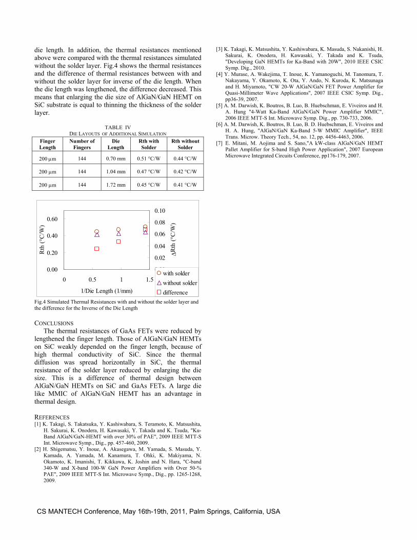
die length. In addition, the thermal resistances mentioned above were compared with the thermal resistances simulated without the solder layer. Fig.4 shows the thermal resistances and the difference of thermal resistances between with and without the solder layer for inverse of the die length. When the die length was lengthened, the difference decreased. This means that enlarging the die size of AlGaN/GaN HEMT on SiC substrate is equal to thinning the thickness of the solder layer.
[3] K. Takagi, K. Matsushita, Y. Kashiwabara, K. Masuda, S. Nakanishi, H. Sakurai, K. Onodera, H. Kawasaki, Y. Takada and K. Tsuda, "Developing GaN HEMTs for Ka-Band with 20W", 2010 IEEE CSIC Symp. Dig., 2010.
[4] Y. Murase, A. Wakejima, T. Inoue, K. Yamanoguchi, M. Tanomura, T. Nakayama, Y. Okamoto, K. Ota, Y. Ando, N. Kuroda, K. Matsunaga and H. Miyamoto, "CW 20-W AlGaN/GaN FET Power Amplifier for Quasi-Millimeter Wave Applications", 2007 IEEE CSIC Symp. Dig., pp36-39, 2007.
[5] A. M. Darwish, K. Boutros, B. Luo, B. Huebschman, E. Viveiros and H. A. Hung "4-Watt Ka-Band AlGaN/GaN Power Amplifier MMIC", 2006 IEEE MTT-S Int. Microwave Symp. Dig., pp. 730-733, 2006. [6] A. M. Darwish, K. Boutros, B. Luo, B. D. Huebschman, E. Viveiros and H. A. Hung, "AlGaN/GaN Ka-Band 5-W MMIC Amplifier", IEEE Trans. Microw. Theory Tech., 54, no. 12, pp. 4456-4463, 2006.
TABLE IV DIE LAYOUTS OF ADDITIONAL SIMULATION
Finger Number of Die Rth with Rth withoutLength Fingers Length Solder Solder
[7] E. Mitani, M. Aojima and S. Sano,"A kW-class AlGaN/GaN HEMT Pallet Amplifier for S-band High Power Application", 2007 European Microwave Integrated Circuits Conference, pp176-179, 2007. 144 0.70 mm 0.51 °C/W 0.44 °C/W 200 μm
200 μm 144 1.04 mm 0.47 °C/W 0.42 °C/W
200 μm 144 1.72 mm 0.45 °C/W 0.41 °C/W
0.00
0.20
0.40
0.60
0 0.5 1 1.5
1/Die Length (1/mm)
Rth
(°C
/W)
0.00
0.02
0.04
0.06
0.08
0.10
ΔRth
(°C
/W)
with solderwithout solderdifference
Fig.4 Simulated Thermal Resistances with and without the solder layer and the difference for the Inverse of the Die Length CONCLUSIONS The thermal resistances of GaAs FETs were reduced by lengthened the finger length. Those of AlGaN/GaN HEMTs on SiC weakly depended on the finger length, because of high thermal conductivity of SiC. Since the thermal diffusion was spread horizontally in SiC, the thermal resistance of the solder layer reduced by enlarging the die size. This is a difference of thermal design between AlGaN/GaN HEMTs on SiC and GaAs FETs. A large die like MMIC of AlGaN/GaN HEMT has an advantage in thermal design. REFERENCES [1] K. Takagi, S. Takatsuka, Y. Kashiwabara, S. Teramoto, K. Matsushita,
H. Sakurai, K. Onodera, H. Kawasaki, Y. Takada and K. Tsuda, "Ku-Band AlGaN/GaN-HEMT with over 30% of PAE", 2009 IEEE MTT-S Int. Microwave Symp., Dig., pp. 457-460, 2009.
[2] H. Shigematsu, Y. Inoue, A. Akasegawa, M. Yamada, S. Masuda, Y. Kamada, A. Yamada, M. Kanamura, T. Ohki, K. Makiyama, N. Okamoto, K. Imanishi, T. Kikkawa, K. Joshin and N. Hara, "C-band 340-W and X-band 100-W GaN Power Amplifiers with Over 50-% PAE", 2009 IEEE MTT-S Int. Microwave Symp., Dig., pp. 1265-1268, 2009.
CS MANTECH Conference, May 16th-19th, 2011, Palm Springs, California, USA
![JICA 201610B 10B 10B 13B 22 10B 11B 11B 26B M2:30 JTñ-ñ-3— … · 2016-10-13 · JICA 201610B 10B 10B 13B 22 10B 11B 11B 26B M2:30 JTñ-ñ-3— JD+ñ3—] (3) @ @ @ 201 2016 11](https://img.dokumen.tips/doc/110x75/5f7b7664c26e297ff6248b8f/jica-201610b-10b-10b-13b-22-10b-11b-11b-26b-m230-jt-3a-2016-10-13-jica.jpg)